28. High-resolution timer (HRTIM)
28.1 Introduction
The high-resolution timer can generate up to 12 digital signals with highly accurate timings. It is primarily intended to drive power conversion systems such as switch mode power supplies or lighting systems, but can be of general purpose usage, whenever a very fine timing resolution is expected.
Its modular architecture allows to generate either independent or coupled waveforms. The wave-shape is defined by self-contained timings (using counters and compare units) and a broad range of external events, such as analog or digital feedbacks and synchronization signals. This allows to produce a large variety of control signal (PWM, phase-shifted, constant \( T_{on} \) ,...) and address most of conversion topologies.
For control and monitoring purposes, the timer has also timing measure capabilities and links to built-in ADC and DAC converters. Last, it features light-load management mode and is able to handle various fault schemes for safe shut-down purposes.
28.2 Main features
- • High-resolution timing units
- – 184 ps resolution, compensated against voltage and temperature variations
- – Duty cycle, frequency, phase shift and pulse width (triggered one-pulse mode) can be adjusted with full resolution, on all outputs
- – 6 16-bit timing units (each one with an independent counter and 4 compare units)
- – 12 outputs that can be controlled by any timing unit, up to 32 set/reset sources per channel
- – Modular architecture to address either multiple independent converters with 1 or 2 switches or few large multi-switch topologies
- • Up to 10 external events, available for any timing unit
- – suitable for peak current control, zero voltage and zero current detection (ZVS and ZCS operation) and counter reset (variable frequency operation)
- – 4 sources per external events (digital inputs, built-in comparators outputs, ADC's analog watchdogs and general purpose timer's trigger outputs)
- – Programmable polarity and edge sensitivity
- – 5 events with a fast asynchronous mode
- – 5 events with a programmable digital filter
- – Spurious events filtering with blanking and windowing modes
- • Direct connections to built-in analog peripherals
- – 10 triggers to ADC converters
- – 9 triggers for DAC converters, among which 6 with slope compensation capabilities
- – Comparator outputs (including filtering and blanking features)
- • Versatile protection scheme
- – suitable for over-current, short-circuit and over-voltage / under-voltage protection
- – 6 fault inputs can be combined and associated to any timing unit
- – 3 sources per fault channel (digital inputs, built-in comparators outputs and external events)
- – Programmable polarity, edge sensitivity, and programmable digital filter
- – Dedicated delayed protections for resonant converters
- • Multiple HRTIM instances can be synchronized with external synchronization inputs/outputs
- • Versatile output stage
- – High-resolution deadtime insertion (down to 735 ps)
- – Programmable output polarity
- – Chopper mode
- • Burst mode controller to handle light-load operation synchronously on multiple converters
- • 8 interrupt vectors, each one with up to 14 sources
- • 7 DMA requests with up to 14 sources, with a burst mode for multiple registers update
28.3 Functional description
28.3.1 General description
The HRTIM can be partitioned into several sub entities:
- • The master timer
- • The timing units (timer A to timer F)
- • The output stage
- • The burst mode controller
- • An external event and fault signal conditioning logic that is shared by all timers
- • The system interface
The master timer is based on a 16-bit up counter. It can set/reset any of the 12 outputs via 4 compare units and it provides synchronization signals to the 6 timer units. Its main purpose is to have the timer units controlled by a unique source. An interleaved buck converter is a typical application example where the master timer manages the phase-shifts between the multiple units.
The timer units are working either independently or coupled with the other timers including the master timer. Each timer contains the controls for two outputs. The outputs set/reset events are triggered either by the timing units compare registers or by events coming from the master timer, from the other timers or from external events.
The output stage has several duties
- • Addition of deadtime when the 2 outputs are configured in complementary PWM mode
- • Addition of a carrier frequency on top of the modulating signal
- • Management of fault events, by asynchronously asserting the outputs to a predefined safe level
The burst mode controller can take over the control of one or multiple timers in case of light-load operation. The burst length and period can be programmed, as well as the idle state of the outputs.
The external event and fault signal conditioning logic includes:
- • The input selection MUXes (for instance for selecting a digital input or an on-chip source for a given external event channel)
- • Polarity and edge-sensitivity programming
- • Digital filtering (for 5 channels out of 12)
The system interface allows the HRTIM to interact with the rest of the MCU:
- • Interrupt requests to the CPU
- • DMA controller for automatic accesses to/from the memories, including an HRTIM specific burst mode
- • Triggers for the ADC and DAC converters
The HRTIM registers are split into 8 groups:
- • Master timer registers
- • Timer A to timer F registers
- • Common registers for features shared by all timer units
Note: As a writing convention, references to the 6 timing units in the text and in registers are generalized using the “x” letter, where x can be any value from A to F.
The block diagram of the timer is shown in Figure 209 .
Figure 209. High-resolution timer overview
The diagram illustrates the internal architecture of the HRTIM. At the top, the
Master timer
is connected to external pins
hrtim_in_sync[3:1]
and
hrtim_out_sync[3:1]
. It receives control signals
hrtim_upd_en[3:1]
,
hrtim_bm_trg
, and
hrtim_bm_ck
. The
Burst mode controller
is also connected to these pins. Below the Master timer are six identical timing units:
TIMER A
,
TIMER B
,
TIMER C
,
TIMER D
,
TIMER E
, and
TIMER F
. Each timer unit contains a
Reset
block, an
Event blanking window
,
4xCMP
(compare) blocks, and
2xCPT
(capture) blocks. These units are interconnected by a
Cross-timer counter reset bus
. A central
Set/reset crossbar
(labeled 'a timer controls 2 outputs') manages signals between the timers. On the left, the
APB and peripheral interface
connects to the
APB bus
and provides control for
DMA burst controller
and
External events conditioning
. External pins include
hrtim_adc_trg[10:1]
,
hrtim_dac_reset_trg[A:F]
,
hrtim_dac_step_trg[A:F]
,
hrtim_dac_trg[3:1]
,
hrtim_it[8:1]
,
hrtim_dma[7:1]
,
hrtim_ker_ck
,
hrtim_pclk
,
hrtim_eev1[4:1]
,
hrtim_eev10[4:1]
, and fault pins
HRTIM_FLT[6:1]
,
hrtim_in_flt[6:1]
, and
hrtim_sys_flt
. The
External events conditioning
block outputs
6 (EEV1_muxout...EEV6_muxout)
to the
Fault conditioning
block. On the right, the
Output stage
generates 12 channels:
HRTIM_CHA1
,
HRTIM_CHA2
,
HRTIM_CHB1
,
HRTIM_CHB2
,
HRTIM_CHC1
,
HRTIM_CHC2
,
HRTIM_CHD1
,
HRTIM_CHD2
,
HRTIM_CHE1
,
HRTIM_CHE2
,
HRTIM_CHF1
, and
HRTIM_CHF2
. Each channel has a
Run/idle
control. The diagram is identified by the code
MSV47425V3
in the bottom right corner.
28.3.2 HRTIM pins and internal signals
The tables in this section summarize the HRTIM inputs and outputs, both on-chip and off-chip.
Table 222. HRTIM inputs/outputs summary
| Signal name | Signal type | Description |
|---|---|---|
| HRTIM_CHA1, HRTIM_CHA2, HRTIM_CHB1, HRTIM_CHB2, HRTIM_CHC1, HRTIM_CHC2, HRTIM_CHD1, HRTIM_CHD2, HRTIM_CHE1, HRTIM_CHE2, HRTIM_CHF1, HRTIM_CHF2 | Outputs | Main HRTIM timer outputs. They can be coupled by pairs (HRTIM_CHx1 & HRTIM_CHx2) with deadtime insertion or work independently. |
| HRTIM_FLT[6:1] hrtim_in_flt[6:1] | Digital input | Fault inputs: immediately disable the HRTIM outputs when asserted (12 on-chip inputs and 6 off-chip HRTIM_FLTx inputs). |
| hrtim_sys_flt | Digital input | System fault gathering MCU internal fault events. |
| hrtim_in_sync[3:1] | Digital Input | Synchronization inputs to synchronize the whole HRTIM with other internal or external timer resources: hrtim_in_sync1: Reserved hrtim_in_sync2: the source is the TIM1_TRGO output (see Table 227: Internal synchronization source ) hrtim_in_sync3: the source is HRTIM_SCIN input pins |
| hrtim_out_sync[2:1] | Digital output | The purpose of this output is to cascade or synchronize several HRTIM instances, either on-chip or off-chip: hrtim_out_sync1: Reserved hrtim_out_sync2: the destination is an off-chip HRTIM or peripheral (via HRTIM_SCOUT output pins) |
| hrtim_eev1[4:1] | Digital input | External events. Each of the 10 events can be selected among 4 sources, either on-chip (from other built-in peripherals: comparator, ADC analog watchdog, TIMx timers, trigger outputs) or off-chip (HRTIM_EEVx input pins). |
| hrtim_eev2[4:1] | ||
| hrtim_eev3[4:1] | ||
| hrtim_eev4[4:1] | ||
| hrtim_eev5[4:1] | ||
| hrtim_eev6[4:1] | ||
| hrtim_eev7[4:1] | ||
| hrtim_eev8[4:1] | ||
| hrtim_eev9[4:1] | ||
| hrtim_eev10[4:1] | ||
| hrtim_upd_en[3:1] | Digital input | A pulse on the update enable inputs hrtim_upd_end[3:1] (on-chip interconnect) triggers the transfer from shadow to active registers |
Table 222. HRTIM inputs/outputs summary (continued)
| Signal name | Signal type | Description |
|---|---|---|
| hrtim_bm_trg | Digital input | A pulse on this input triggers a burst mode entry. This input is connected to an internal source (see Table 226: Burst mode trigger source ). |
| hrtim_bm_ck[4:1] | Digital input | Burst mode clock (on-chip interconnect) |
| hrtim_adc_trg[10:1] | Digital output | ADC start of conversion triggers. The hrtim_adc_trg1 .. hrtim_adc_trg10 outputs are here-after referred to as ADC trigger 1 to ADC trigger 10. |
| hrtim_dac_trg[3:1] | Digital output | DAC conversion update triggers |
| hrtim_dac_reset_trg[6:1] hrtim_dac_step_trg[6:1] | Digital output | Dual channel DAC triggers |
| hrtim_it[8:1] | Digital output | Interrupt requests |
| hrtim_dma[7:1] | Digital output | DMA requests |
| hrtim_pclk | - | APB clock |
| hrtim_ker_ck | - | HRTIM kernel clock |
Table 223. External events mapping and associated features
| External event channel | Fast mode | Digital filter | Balanced fault timer A,B,C | Balanced fault timer D,E,F | Source (EExSRC[1:0]) | Comparator and input sources available per package | ||||
|---|---|---|---|---|---|---|---|---|---|---|
| Src1 (00) | Src2 (01) | Src3 (10) | Src4 (11) | 48-pin | 64-pin and 100-pin | |||||
| hrtim_eev 1[4:1] | Yes | - | - | - | PC12 | COMP2 | tim1_trgo | adc1_awd1 | Comp | Comp & input |
| hrtim_eev 2[4:1] | Yes | - | - | - | PC11 | COMP4 | tim2_trgo | adc1_awd2 | Comp | Comp & input |
| hrtim_eev 3[4:1] | Yes | - | - | - | PB7 | COMP6 | tim3_trgo | adc1_awd3 | Comp & input | Comp & input |
| hrtim_eev 4[4:1] | Yes | - | - | - | PB6 | COMP1 | COMP5 | adc2_awd1 | Comp & input | Comp & input |
| hrtim_eev 5[4:1] | Yes | - | - | - | PB9 | COMP3 | COMP7 | adc2_awd2 | Comp & input | Comp & input |
| hrtim_eev 6[4:1] | - | Yes | Yes | - | PB5 | COMP2 | COMP1 | adc2_awd3 | Comp & input | Comp & input |
| hrtim_eev 7[4:1] | - | Yes | Yes | - | PB4 | COMP4 | tim7_trgo | adc3_awd1 | Comp & input | Comp & input |
| hrtim_eev 8[4:1] | - | Yes | - | Yes | PB8 | COMP6 | COMP3 | adc4_awd1 | Comp & input | Comp & input |
| hrtim_eev 9[4:1] | - | Yes | - | Yes | PB3 | COMP5 | tim15_trgo | COMP4 | Comp & input | Comp & input |
| hrtim_eev 10[4:1] | - | Yes | - | - | PC5/PC6 | COMP7 | tim6_trgo | adc5_awd1 | - | Comp & input |
Table 224. Update enable inputs and sources
| hrtim_upd_en[3:1] | Update source |
|---|---|
| hrtim_upd_en1 | tim16_oc1 |
| hrtim_upd_en2 | tim17_oc1 |
| hrtim_upd_en3 | tim6_trgo |
Table 225. Burst mode clock sources
| hrtim_bm_ck[4:1] | BMCLK[3:0] | Clock source |
|---|---|---|
| hrtim_bm_ck1 | 0110 | tim16_oc1 |
| hrtim_bm_ck2 | 0111 | tim17_oc1 |
| hrtim_bm_ck3 | 1000 | tim17_trgo |
| hrtim_bm_ck4 | 1001 | Reserved |
Table 226. Burst mode trigger source
| - | trigger source |
|---|---|
| hrtim_bm_trg | tim7_trgo |
Table 227. Internal synchronization source
| - | synchronization source |
|---|---|
| hrtim_in_sync2 | tim1_trgo |
Table 228. Fault inputs
| Fault channel | External Input FLTxSRC[1:0] = 00 HRTIM_FLT[6:1] | On-chip source FLTxSRC[1:0] = 01 hrtim_in_flt[6:1] | On-chip source FLTxSRC[1:0] = 10 hrtim internal | On-chip source FLTxSRC[1:0] = 11 hrtim internal |
|---|---|---|---|---|
| Fault 1 | PA12 | COMP2 | EEV1_muxout | N/A |
| Fault 2 | PA15 | COMP4 | EEV2_muxout | N/A |
| Fault 3 | PB10 | COMP6 | EEV3_muxout | N/A |
| Fault 4 | PB11 | COMP1 | EEV4_muxout | N/A |
| Fault 5 | PB0/PC7 | COMP3 | EEV5_muxout | N/A |
| Fault 6 | PC10 | COMP5 | EEV6_muxout | N/A |
Table 229. HRTIM DAC triggers connections
| HRTIM DAC triggers | DAC1_CH1 DAC_CH2 | DAC2_CH1 | DAC3_CH1 DAC3_CH2 | DAC4_CH1 DAC4_CH2 |
|---|---|---|---|---|
| hrtim_dac_trg1 | Yes | - | - | Yes |
| hrtim_dac_trg2 | - | Yes | - | - |
| hrtim_dac_trg3 | - | - | Yes | - |
| hrtim_dac_reset_trg1 hrtim_dac_step_trg1 | Yes | Yes | Yes | Yes |
| hrtim_dac_reset_trg2 hrtim_dac_step_trg2 | Yes | Yes | Yes | Yes |
| hrtim_dac_reset_trg3 hrtim_dac_step_trg3 | Yes | Yes | Yes | Yes |
| hrtim_dac_reset_trg4 hrtim_dac_step_trg4 | Yes | Yes | Yes | Yes |
| hrtim_dac_reset_trg5 hrtim_dac_step_trg5 | Yes | Yes | Yes | Yes |
| hrtim_dac_reset_trg6 hrtim_dac_step_trg6 | Yes | Yes | Yes | Yes |
| Source | Enable bit in SYSCFGR2 register |
|---|---|
| Cortex®-M4 with FPU LOCKUP | CLL |
| Programmable Voltage Detector (PVD) | PVDL |
| SRAM parity error | SPL |
| Flash double ECC error | ECCL |
| Clock Security System (CSS) | None (always enabled) |
28.3.3 Clocks
The HRTIM must be supplied by the \( t_{HRTIM} \) APB2 clock to offer a full resolution. The \( t_{HRTIM} \) clock period is evenly divided into up to 32 intermediate steps using an edge positioning logic. All clocks present in the HRTIM are derived from this reference clock.
Definition of terms
- \( f_{HRTIM} \) : main HRTIM clock (hrtim_ker_ck). All subsequent clocks are derived and synchronous with this source.
- \( f_{HRCK} \) : high-resolution equivalent clock. Considering the \( f_{HRTIM} \) clock period division by 32, it is equivalent to a frequency of \( 32 \times f_{HRTIM} \) .
- \( f_{DTG} \) : deadtime generator clock. For convenience, only the \( t_{DTG} \) period ( \( t_{DTG} = 1/f_{DTG} \) ) is used in this document.
- \( f_{CHPFRQ} \) : chopper stage clock source.
- \( f_{1STPW} \) : clock source defining the length of the initial pulse in chopper mode. For convenience, only the \( t_{1STPW} \) period ( \( t_{1STPW} = 1/f_{1STPW} \) ) is used in this document.
- \( f_{BRST} \) : burst mode controller counter clock.
- \( f_{SAMPLING} \) : clock needed to sample the fault or the external events inputs.
- \( f_{FLTS} \) : clock derived from \( f_{HRTIM} \) which is used as a source for \( f_{SAMPLING} \) to filter fault events.
- \( f_{EEVS} \) : clock derived from \( f_{HRTIM} \) which is used as a source for \( f_{SAMPLING} \) to filter external events.
Timer clock and prescaler
Each timer in the HRTIM has its own individual clock prescaler, which allows you to adjust the timer resolution (see Table 231 ).
Table 231. Timer resolution and min. PWM frequency for \( f_{HRTIM} = 170 \) MHz| CKPSC[2:0] | Prescaling ratio | \( f_{HRCK} \) equivalent frequency | Resolution | Min PWM frequency |
|---|---|---|---|---|
| 000 | 1 | \( 170 \times 32 \) MHz = 5.44 GHz | 184 ps | 83.0 kHz |
| 001 | 2 | \( 170 \times 16 \) MHz = 2.72 GHz | 368 ps | 41.5 kHz |
| 010 | 4 | \( 170 \times 8 \) MHz = 1.36 GHz | 735 ps | 20.8 kHz |
| CKPSC[2:0] | Prescaling ratio | \(
f_{HRCK}
\) equivalent frequency | Resolution | Min PWM frequency |
|---|---|---|---|---|
| 011 | 8 | \( 170 \times 4\text{ MHz} = 680\text{ MHz} \) | 1.47 ns | 10.4 kHz |
| 100 | 16 | \( 170 \times 2\text{ MHz} = 340\text{ MHz} \) | 2.94 ns | 5.19 kHz |
| 101 | 32 | 170 MHz | 5.88 ns | 2.59 kHz |
| 110 | 64 | \( 170/2\text{ MHz} = 85\text{ MHz} \) | 11.76 ns | 1.30 kHz |
| 111 | 128 | \( 170/4\text{ MHz} = 42.5\text{ MHz} \) | 23.53 ns | 0.65 kHz |
The high-resolution is available for edge positioning, PWM period adjustment and externally triggered pulse duration.
The high-resolution is not available for the following features
- • Timer counter read and write accesses
- • Capture unit
For clock prescaling ratios below 32 (CKPSC[2:0] < 5), the least significant bits of the counter and capture registers are not significant. The least significant bits cannot be written (counter register only) and return 0 when read.
For instance, if CKPSC[2:0] = 2 (prescaling by 4), writing 0xFFFF into the counter register yields an effective value of 0xFFF8. Conversely, any counter value between 0xFFFF and 0xFFF8 is read as 0xFFF8.
Figure 210. Counter and capture register format vs clock prescaling factor
b15 b0 Prescaling
1
2
4
8
16
32
Significant bit: read returns effective value
Not significant bit: read returns 0
MS32257V1
Initialization
At start-up, it is mandatory to initialize first the prescaler bitfields before writing the compare and period registers. Once the timer is enabled (MCEN or TxCEN bit set in the HRTIM_MCR register), the prescaler cannot be modified.
When multiple timers are enabled, the prescalers are synchronized with the prescaler of the timer that was started first.
Warning: It is possible to have different prescaling ratios in the master and TIMA..E timers only if the counter and output behavior does not depend on other timers' information and signals. It is mandatory to configure identical prescaling ratios in these timers when one of the following events is propagated from one timing unit (or master timer) to another: output set/reset event, counter reset event, update event, external event filter or capture triggers. Prescaler factors not equal yield to unpredictable results.
Deadtime generator clock
The deadtime prescaler is supplied by \( (f_{\text{HRTIM}} \times 8) / 2^{(\text{DTPRSC}[2:0])} \) , programmed with DTPRSC[2:0] bits in the HRTIM_DTxR register.
\( t_{\text{DTG}} \) ranges from 735 ps to 94.1 ns for \( f_{\text{HRTIM}} = 170 \text{ MHz} \) .
Chopper stage clock
The chopper stage clock source \( f_{\text{CHPFRQ}} \) is derived from \( f_{\text{HRTIM}} \) with a division factor ranging from 16 to 256, so that \( 664 \text{ kHz} \leq f_{\text{CHPFRQ}} \leq 10.625 \text{ MHz} \) for \( f_{\text{HRTIM}} = 170 \text{ MHz} \) .
\( t_{\text{ISTPW}} \) is the length of the initial pulse in chopper mode, programmed with the STRPW[3:0] bits in the HRTIM_CHPxR register, as follows:
It uses \( f_{\text{HRTIM}} / 16 \) as clock source (10.625 MHz for \( f_{\text{HRTIM}} = 170 \text{ MHz} \) ).
Burst mode prescaler
The burst mode controller counter clock \( f_{\text{BRST}} \) can be supplied by several sources, among which one is derived from \( f_{\text{HRTIM}} \) .
In this case, \( f_{\text{BRST}} \) ranges from \( f_{\text{HRTIM}} \) to \( f_{\text{HRTIM}} / 32768 \) (5.19 kHz for \( f_{\text{HRTIM}} = 170 \text{ MHz} \) ).
Fault input sampling clock
The fault input noise rejection filter has a time constant defined with \( f_{\text{SAMPLING}} \) which can be either \( f_{\text{HRTIM}} \) or \( f_{\text{FLTS}} \) .
\( f_{\text{FLTS}} \) is derived from \( f_{\text{HRTIM}} \) and ranges from 170 MHz to 21.25 MHz for \( f_{\text{HRTIM}} = 170 \text{ MHz} \) .
External event input sampling clock
The fault input noise rejection filter has a time constant defined with \( f_{\text{SAMPLING}} \) which can be either \( f_{\text{HRTIM}} \) or \( f_{\text{EEVS}} \) .
\( f_{\text{EEVS}} \) is derived from \( f_{\text{HRTIM}} \) and ranges from 170 MHz to 21.25 MHz for \( f_{\text{HRTIM}} = 170 \text{ MHz} \) .
28.3.4 Timer A..F timing units
The HRTIM embeds 6 identical timing units made of a 16-bit up-counter with an auto-reload mechanism to define the counting period, 4 compare and 2 capture units, as per Figure 211. Each unit includes all control features for 2 outputs, so that it operates as a standalone timer.
Figure 211. Timer A..F overview
The diagram illustrates the internal architecture of a Timer A..F timing unit. At its core is a Counter block. This counter receives a clock signal from \( f_{HRTIM} \) via a Prescaler . It also receives a RST signal from Reset Management . The counter's output is connected to Capture 1 and Capture 2 blocks, which generate CPT1 and CPT2 interrupt/DMA requests. The counter also feeds into a Repetition Counter (producing REP output) and a Period block. The Period block connects to Compare 1 through Compare 4 blocks. Each compare block generates a CMP interrupt/DMA request (e.g., CMP1 through CMP4 ). Compare 1 and Compare 3 are associated with a Half block, while Compare 2 and Compare 4 are associated with an Autodelay block. The compare blocks also feed into a Set / reset crossbar (2 outputs) block, which produces Out 1 and Out 2 signals to the output stage. This crossbar block also receives REP , CMP1 , CMP2 , CMP3 , CMP4 , and Update signals. It is preceded by a Push-pull and deadtime management block, which in turn receives signals from an Events Blanking and windowing block. This block receives 10 signals from external events conditioning . The entire unit is also influenced by a Master timer (6 signals) and Other timing units (9 signals). A legend indicates that a double-outlined box represents a Register with preload, and a jagged arrow represents an Interrupt / DMA request . The diagram is identified by the code MS32258V1.
The period and compare values must be within a lower and an upper limit related to the high-resolution implementation and listed in Table 232:
- • The minimum value must be greater than or equal to 3 periods of the \( f_{HRTIM} \) clock. The value 0x0000 can be written in CMP1 and CMP3 registers only, to skip a PWM pulse. See Section : Null duty cycle exception case for details
- • The maximum value must be less than or equal to 0xFFFF - 1 periods of the \( f_{HRTIM} \) clock.
| CKPSC[2:0] value | Min (1) | Max |
|---|---|---|
| 0 | 0x0060 | 0xFFDF |
| 1 | 0x0030 | 0xFFEF |
| 2 | 0x0018 | 0xFFF7 |
| 3 | 0x000C | 0xFFFB |
| 4 | 0x0006 | 0xFFFD |
| ≥ 5 | 0x0003 | 0xFFFD |
- 1. The value 0x0000 can be written in CMP1 and CMP3 registers only, to skip a PWM pulse. See Section : Null duty cycle exception case for details.
Note: A compare value greater than the period register value does not generate a compare match event.
Counter operating mode
Timer A..F operate in continuous (free-running) mode or in single-shot manner where counting is started by a reset event, using the CONT bit in the HRTIM_TIMxCR control register. An additional RETRIG bit allows you to select whether the single-shot operation is retriggerable or non-retriggerable. Details of operation are summarized on Table 233 and on Figure 212 and Figure 213 .
Table 233. Timer operating modes| CONT | RETRIG | Operating mode | Start / stop conditions Clocking and event generation |
|---|---|---|---|
| 0 | 0 | Single-shot Non-retriggerable | Setting the TxEN bit enables the timer but does not start the counter. A first reset event starts the counting and any subsequent reset is ignored until the counter reaches the PER value. The PER event is then generated and the counter is stopped. A reset event re-starts the counting operation from 0x0000. |
| 0 | 1 | Single-shot Retriggerable | Setting the TxEN bit enables the timer but does not start the counter. A reset event starts the counting if the counter is stopped, otherwise it clears the counter. When the counter reaches the PER value, the PER event is generated and the counter is stopped. A reset event re-starts the counting operation from 0x0000. |
| 1 | X | Continuous mode | Setting the TxEN bit enables the timer and starts the counter simultaneously. When the counter reaches the PER value, it rolls-over to 0x0000 and resumes counting. The counter can be reset at any time. |
The TxEN bit can be cleared at any time to disable the timer and stop the counting.
Figure 212. Continuous timer operation
Timing diagram for continuous timer operation. The diagram shows four signals over time: PER (dashed line), Counter (solid line), Reset (solid line), and Enable (solid line). The Counter signal is a sawtooth wave that increases linearly and then resets to zero. The Reset signal is a series of pulses. The Enable signal is a single pulse that starts the timer. The text 'Continuous mode (CONT = 1, RETRIG = X)' is shown at the bottom. The reference 'MS32259V1' is in the bottom right corner.
Figure 213. Single-shot timer operation
Timing diagrams for single-shot timer operation. The figure contains two diagrams. The top diagram shows 'Single-shot mode, non-retriggerable (CONT = 0, RETRIG = 0)'. It displays four signals: PER (dashed line), Counter (solid line), Reset* (solid line), and Enable (solid line). The Counter signal is a sawtooth wave that increases linearly and then resets to zero. The Reset* signal is a series of pulses, some of which are marked with an 'X' to indicate they are ignored because the timer is still running. The Enable signal is a single pulse that starts the timer. The bottom diagram shows 'Single-shot mode, retriggerable (CONT = 0, RETRIG = 1)'. It displays the same four signals. In this mode, a new PER event while the timer is still running restarts the counter. A legend at the bottom left explains the Reset* signal: a solid line represents 'Reset active' and a line with an 'X' represents 'Reset ignored'. The reference 'MS32260V1' is in the bottom right corner.
Roll-over event
A counter roll-over event is generated when the counter goes back to 0 after having reached the period value set in the HRTIM_PERxR register in continuous mode.
This event is used for multiple purposes in the HRTIM:
- – To set/reset the outputs
- – To trigger the register content update (transfer from preload to active)
- – To trigger an IRQ or a DMA request
- – To serve as a burst mode clock source or a burst start trigger
- – As an ADC trigger
- – To decrement the repetition counter
If the initial counter value is above the period value when the timer is started, or if a new period is set while the counter is already above this value, the counter is not reset: it overflows at the maximum period value and the repetition counter does not decrement.
Timer reset
The reset of the timing unit counter can be triggered by up to 30 events that can be selected simultaneously in the HRTIM_RSTxR register, among the following sources:
- – The timing unit: compare 2, compare 4 and update (3 events)
- – The master timer: reset and compare 1..4 (5 events)
- – The external events EXTEVNT1..10 (10 events)
- – All other timing units (e.g. timer B..F for timer A): compare 1, 2 and 4 (12 events)
Several events can be selected simultaneously to handle multiple reset sources. In this case, the multiple reset requests are ORed. When 2 counter reset events are generated within the same \( f_{\text{HRTIM}} \) clock cycle, the last counter reset is taken into account.
Additionally, it is possible to do a software reset of the counter using the TxRST bits in the HRTIM_CR2 register. These control bits are grouped into a single register to allow the simultaneous reset of several counters.
The reset requests are taken into account only once the related counters are enabled (TxCEN bit set).
When the \( f_{\text{HRTIM}} \) clock prescaling ratio is above 32 (counting period above \( f_{\text{HRTIM}} \) ), the counter reset event is delayed to the next active edge of the prescaled clock. This allows to maintain a jitterless waveform generation when an output transition is synchronized to the reset event (typically a constant Ton time converter).
Figure 214 shows how the reset is handled for a clock prescaling ratio of 128 ( \( f_{\text{HRTIM}} \) divided by 4).
Figure 214. Timer reset resynchronization (prescaling ratio above 32)
HRTIM_CHA1: Set on Timer A reset event, Reset on Compare 1 = 2
MS32261V2
Repetition counter
A common software practice is to have an interrupt generated when the period value is reached, so that the maximum amount of time is left for processing before the next period begins. The main purpose of the repetition counter is to adjust the period interrupt rate and off-load the CPU by decoupling the switching frequency and the interrupt frequency.
The timing units have a repetition counter. This counter cannot be read, but solely programmed with an auto-reload value in the HRTIM_REPxR register.
The repetition counter is initialized with the content of the HRTIM_REPxR register when the timer is enabled (TXCEN bit set). Once the timer has been enabled, any time the counter is cleared, either due to a reset event or due to a counter roll-over, the repetition counter is decreased. When it reaches zero, a REP interrupt or a DMA request is issued if enabled (REPIE and REPDE bits in the HRTIM_DIER register).
If the HRTIM_REPxR register is set to 0, an interrupt is generated for each and every period. For any value above 0, a REP interrupt is generated after (HRTIM_REPxR + 1) periods. Figure 215 presents the repetition counter operation for various values, in continuous mode.
Figure 215. Repetition rate versus HRTIM_REPxR content in continuous mode
The diagram illustrates the relationship between the Period (PER), the Counter, and the HRTIM_REPxR register content in continuous mode. The top section shows the PER signal as a sawtooth wave and the Counter as a series of sawtooth waves that reset when they reach the PER value. Below this, three rows show the HRTIM_REPxR register content and the resulting REP (Repetition) events for different repetition rates.
- HRTIM_REPxR = 0: The counter values are 0*, 0*, 0*, 0*. REP events occur at every counter reset.
- HRTIM_REPxR = 1: The counter values are 0*, 1*, 0*, 1*. REP events occur every two counter cycles.
- HRTIM_REPxR = 2: The counter values are 1*, 0*, 2*, 0*. REP events occur every three counter cycles.
* denotes repetition counter internal values (not readable, for explanation purpose only)
MS32262V1
The repetition counter can also be used when the counter is reset before reaching the period value (variable frequency operation) either in continuous or in single-shot mode (Figure 216 here-below). The reset causes the repetition counter to be decremented, at the exception of the very first start following counter enable (TxCEN bit set).
Figure 216. Repetition counter behavior in single-shot mode
The diagram illustrates the repetition counter behavior in single-shot mode. The top section shows the PER signal as a sawtooth wave and the Counter as a series of sawtooth waves that reset when they reach the PER value. The Reset signal is shown as a series of pulses. The bottom section shows the HRTIM_REPxR register content and the resulting REP (Repetition) events for different repetition rates.
- The counter values are 2*, 1*, 0*, 2*, 1*, 0*.
- REP events occur at the 0* counter value.
* denotes repetition counter internal values (not readable, for explanation purpose only)
MS32263V1
A reset or start event from the HRTIM_SCIN[3:1] source causes the repetition to be decremented as any other reset. However, in SYNCIN-started single-shot mode (SYNCSTRTx bit set in the HRTIM_TIMxCR register), the repetition counter is decremented only on the 1st reset event following the period. Any subsequent reset does not alter the repetition counter until the counter is re-started by a new request on HRTIM_SCIN[3:1] inputs.
Set / reset crossbar
A “set” event correspond to a transition to the output active state, while a “reset” event corresponds to a transition to the output inactive state.
The polarity of the waveform is defined in the output stage to accommodate positive or negative logic external components: an active level corresponds to a logic level 1 for a positive polarity (POLx = 0), and to a logic level 0 for a negative polarity (POLx = 1).
Each of the timing units handles the set/reset crossbar for two outputs. These 2 outputs can be set, reset or toggled by up to 32 events that can be selected among the following sources:
- – The timing unit: period, compare 1..4, register update (6 events)
- – The master timer: period, compare 1..4, HRTIM synchronization (6 events)
- – All other timing units (e.g. timer B..F for timer A): TIMEVNT1..9 (9 events described in Table 234 )
- – The external events EXTEVNT1..10 (10 events)
- – A software forcing (1 event)
Note: In up/down mode (UDM bit set to 1), the counter period event is defined as per the OUTROM[1:0] bit setting.
The event sources are ORed and multiple events can be simultaneously selected.
Each output is controlled by two 32-bit registers, one coding for the set (HRTIM_SETxyR) and another one for the reset (HRTIM_RSTxyR), where x stands for the timing unit: A..F and y stands for the output 1 or 2 (e.g. HRTIM_SETA1R, HRTIM_RSTC2R,...).
If the same event is selected for both set and reset, it toggles the output. It is not possible to toggle the output state more than one time per \( t_{\text{HRTIM}} \) period: in case of two consecutive toggling events within the same cycle, only the first one is considered.
The set and reset requests are taken into account only once the counter is enabled (TxCEN bit set), except if the software is forcing a request to allow the prepositioning of the outputs at timer start-up.
Table 234 summarizes the events from other timing units that can be used to set and reset the outputs. The number corresponds to the timer events (such as TIMEVNTx) listed in the register, and empty locations are indicating non-available events.
For instance, timer A outputs can be set or reset by the following events: timer B compare 1 and 2, timer C compare 2 and 3,... and timer E compare 3 is listed as TIMEVNT7 in HRTIM_SETA1R.
Table 234. Events mapping across timer A to F
| Source | Timer A | Timer B | Timer C | Timer D | Timer E | Timer F | |||||||||||||||||||
|---|---|---|---|---|---|---|---|---|---|---|---|---|---|---|---|---|---|---|---|---|---|---|---|---|---|
| CMP1 | CMP2 | CMP3 | CMP4 | CMP1 | CMP2 | CMP3 | CMP4 | CMP1 | CMP2 | CMP3 | CMP4 | CMP1 | CMP2 | CMP3 | CMP4 | CMP1 | CMP2 | CMP3 | CMP4 | CMP1 | CMP2 | CMP3 | CMP4 | ||
| Destination | TA | - | - | - | - | 1 | 2 | - | - | - | 3 | 4 | - | 5 | 6 | - | - | - | - | 7 | 8 | - | - | - | 9 |
| TB | 1 | 2 | - | - | - | - | - | - | - | - | 3 | 4 | - | - | 5 | 6 | 7 | 8 | - | - | - | - | 9 | - | |
| TC | - | 1 | 2 | - | - | 3 | 4 | - | - | - | - | - | 5 | - | 6 | - | - | - | 7 | 8 | - | 9 | - | - | |
| TD | 1 | - | - | 2 | - | 3 | - | 4 | - | - | - | 5 | - | - | - | - | 6 | - | - | 7 | 8 | - | 9 | - | |
| TE | - | - | - | 1 | - | - | 2 | 3 | 4 | 5 | - | - | 6 | 7 | - | - | - | - | - | - | - | - | 8 | 9 | |
| TF | - | - | 1 | - | 2 | - | - | 3 | 4 | - | - | 5 | - | - | 6 | 7 | - | 8 | 9 | - | - | - | - | - | |
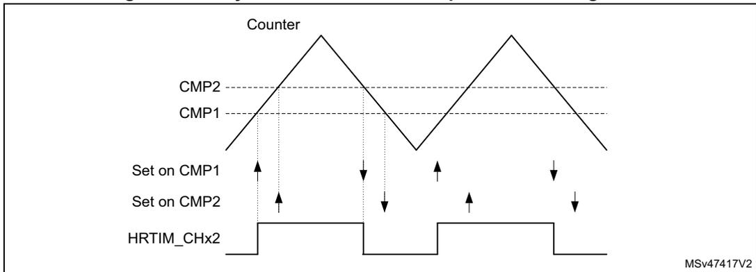
Figure 217 represents how a PWM signal is generated using two compare events.
Figure 217. Compare events action on outputs: set on compare 1, reset on compare 2
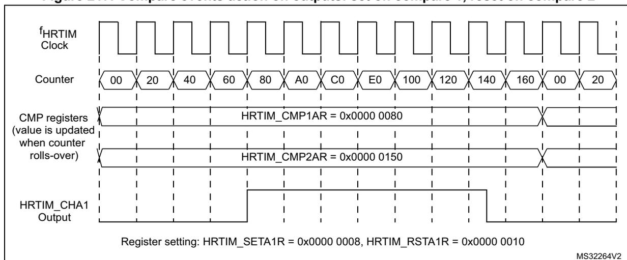
Timing diagram illustrating the generation of a PWM signal using compare events. The diagram shows the relationship between the HRTIM Clock, Counter, CMP registers, and the HRTIM_CHA1 Output.
- f HRTIM Clock: A periodic square wave clock signal.
- Counter: A counter that increments from 00 to 160, then rolls over to 00 and continues to 20. The counter value is updated when the counter rolls-over.
- CMP registers:
Two compare registers are shown:
- HRTIM_CMP1AR = 0x0000 0080
- HRTIM_CMP2AR = 0x0000 0150
- HRTIM_CHA1 Output: A square wave output that is set high when the counter reaches the value in HRTIM_CMP1AR (80) and reset low when the counter reaches the value in HRTIM_CMP2AR (150).
Register setting: HRTIM_SETA1R = 0x0000 0008, HRTIM_RSTA1R = 0x0000 0010
MS32264V2
Set / reset on update events
A set or reset event on update is done at low resolution. When CKPSC[2:0] < 5, the high-resolution delay is set to its maximum value so that a set/reset event on update always lags as compared to other compare set/reset events, with a jitter varying between 0 and 31/32 of a f HRTIM clock period.
Half mode
This mode aims at generating square signal with fixed 50% duty cycle and variable frequency (typically for converters using resonant topologies). It allows to have the duty cycle automatically forced to half of the period value when a new period is programmed.
This mode is enabled by writing HALF bit to 1 in the HRTIM_TIMxCR register. When the HRTIM_PERxR register is written, it causes an automatic update of the compare 1 value with HRTIM_PERxR/2 value.
The output on which a square wave is generated must be programmed to have one transition on CMP1 event, and one transition on the period event, as follows:
- – HRTIM_SETxyR = 0x0000 0008, HRTIM_RSTxyR = 0x0000 0004, or
- – HRTIM_SETxyR = 0x0000 0004, HRTIM_RSTxyR = 0x0000 0008
The HALF mode overrides the content of the HRTIM_CMP1xR register. The access to the HRTIM_PERxR register only causes compare 1 internal register to be updated. The user-accessible HRTIM_CMP1xR register is not updated with the HRTIM_PERxR / 2 value.
When the preload is enabled (PREEN = 1, MUDIS, TxUDIS), compare 1 active register is refreshed on the update event. If the preload is disabled (PREEN= 0), compare 1 active register is updated as soon as HRTIM_PERxR is written.
The period must be greater than or equal to 6 periods of the \( f_{HRTIM} \) clock (0xC0 if CKPSC[2:0] = 0, 0x60 if CKPSC[2:0] = 1, 0x30 if CKPSC[2:0] = 2,...) when the HALF mode is enabled.
Interleaved mode
This mode complements the Half mode and helps the implementation of interleaved topologies.
It allows to re-compute automatically the content of compare registers when the HRTIM_PERxR value is updated.
The selection is done using the HALF bit and the IL[1:0] bits in HRTIM_MCR and HRTIM_TIMxCR registers, as shown on the Table 235 below.
Table 235. Interleaved mode selection
| HALF bit | INTLVD [1:0] bits | Mode |
|---|---|---|
| 0 | 00 | Disabled |
| 0 | 01 | Triple interleaved (120°) |
| 0 | 10 | Quad interleaved (90°) |
| 0 | 11 | Reserved |
| 1 | xx | Dual interleaved (180°) |
Table 236 gives the compare values for the 3 available modes. The content of the compare registers is overridden. The corresponding compare events can be used to trigger an output set / reset or to reset a slave timer.
Table 236. Compare 1..3 values in interleaved mode
| Mode | Dual interleaved 180° | Triple interleaved 120° | Quad interleaved 90° |
|---|---|---|---|
| CMP1 value | PERxR/2 | PERxR/3 | PERxR/4 |
| CMP2 value | Not affected | 2x (PERxR/3) | PERxR/2 |
| CMP3 value | Not affected | Not affected | 3x (PERxR/4) |
Note: In half and interleaved modes, the compare registers are controlled by hardware and writing them has no effect. However the written value is stored in the preload register and becomes active on the update event following the exit of these modes.
Note: The triple and quad interleaved modes must not be used simultaneously with other modes using CMP2 (dual channel dac trigger and triggered-half modes).
Null duty cycle exception case
The high-resolution behavior is not supported for pulses narrower than 3 \( t_{HRTIM} \) periods (see Section 28.3.7: Set / reset events priorities and narrow pulses management ) and any value strictly below 3 periods of the \( f_{HRTIM} \) clock (that is 0x60 if CKPSC[2:0] = 0, 0x30 if CKPSC[2:0] = 1, 0x18 if CKPSC[2:0] = 2,...) in the HRTIM_TIMxCMPy register is forbidden (see 28.5.19: HRTIM timer x compare 1 register (HRTIM_CMP1xR) (x = A to F) ).
However, it is possible to skip an output pulse and have a null duty cycle by simply writing a null value in the following two registers: HRTIM_TIMxCMP1 and HRTIM_TIMxCMP3, if and only if the following conditions are met:
- – the output SET event is generated by the PERIOD event
- – the output RESET if generated by the compare 1 (respectively compare 3) event
- – the compare 1 (compare 3) event is active within the timer unit itself, and not used for other timing units
For any other use case, this can be done by programming the SET and RESET events with the very same compare values, above 3 periods of the \( f_{HRTIM} \) clock. In this case, the output is reset forced (following the set/reset priority scheme defined in the Section 28.3.7: Set / reset events priorities and narrow pulses management ).
Swap mode
This mode allows to swap the two outputs with a single bit access: the output 1 signal is connected to the output 2 pin and the output 2 signal is connected to output 1 pin. The output swap is triggered with the SWPx bits in the HRTIM_CR2 register and is effective on the next update event.
The outputs are swapped prior to the set/reset crossbar unit, as following:
- – if SWPx = 0, HRTIM_SETx1R and HRTIM_RSTx1R are coding for the output 1, HRTIM_SETx2R and HRTIM_RSTx2R are coding for the output 2
- – if SWPx = 1, HRTIM_SETx1R and HRTIM_RSTx1R are coding for the output 2, HRTIM_SETx2R and HRTIM_RSTx2R are coding for the output 1
The swap mode is only affecting the preload register, and not the active registers.
Note: The preload mode must be enabled when using the swap mode.
Consequently, it does not modify the auxiliary outputs in parallel with the regular outputs going to the output stage (see Section 28.3.18 for details). They provide the following internal status, events and signals:
- – O1CPY, O2CPY, SETxy and RSTxy status flags, together with the corresponding interrupts and DMA requests
- – Capture triggers upon output set/reset (TA2, TB2, TC2, TD2, TE2, TF2)
- – External event filters generated with a Tx2 output copy
For instance the SETx1 flag is related to the output 1 when SWP = 0 and is related to the output 2 when SWPx = 1.
Similarly, the swap mode does not change the attribution of control bits in the HRTIM_OUTxR register (DIDLx, CHPx, FAULTx[1:0], IDLESx, POLx bits). For instance, the POL1 bit controls the output 1 polarity whatever the SWP bit value.
Note: The SWPx bits are ignored in push-pull mode (PSHPLL = 1 in the HRTIM_TIMxCR register).
Capture
The timing unit has the capability to capture the counter value, triggered by internal and external events. The purpose is to:
- – measure events arrival timings or occurrence intervals
- – update compare 2 and compare 4 values in auto-delayed mode (see Section : Auto-delayed mode ).
The capture is done with \( f_{HRTIM} \) resolution: for a clock prescaling ratio below 32 (CKPSC[2:0] < 5), the least significant bits of the register are not significant (read as 0).
The timer has 2 capture registers: HRTIM_CPT1xR and HRTIM_CPT2xR. The capture triggers are programmed in the HRTIM_CPT1xCR and HRTIM_CPT2xCR registers.
The capture of the timing unit counter can be triggered by up to 28 events that can be selected simultaneously in the HRTIM_CPT1xCR and HRTIM_CPT2xCR registers, among the following sources:
- • The external events, EXTEVNT1..10 (10 events)
- • All other timing units (e.g. timer B..F for timer A): compare 1, 2 and output 1 set/reset events (16 events)
- • The timing unit: update (1 event)
- • A software capture (1 event)
Several events can be selected simultaneously to handle multiple capture triggers. In this case, the concurrent trigger requests are ORed. The capture can generate an interrupt or a DMA request when CPTxE and CPTxDE bits are set in the HRTIM_TIMxDIER register.
Over-capture is not prevented by the circuitry: a new capture is triggered even if the previous value was not read, or if the capture flag was not cleared.
Figure 218. Timer A timing unit capture circuitry
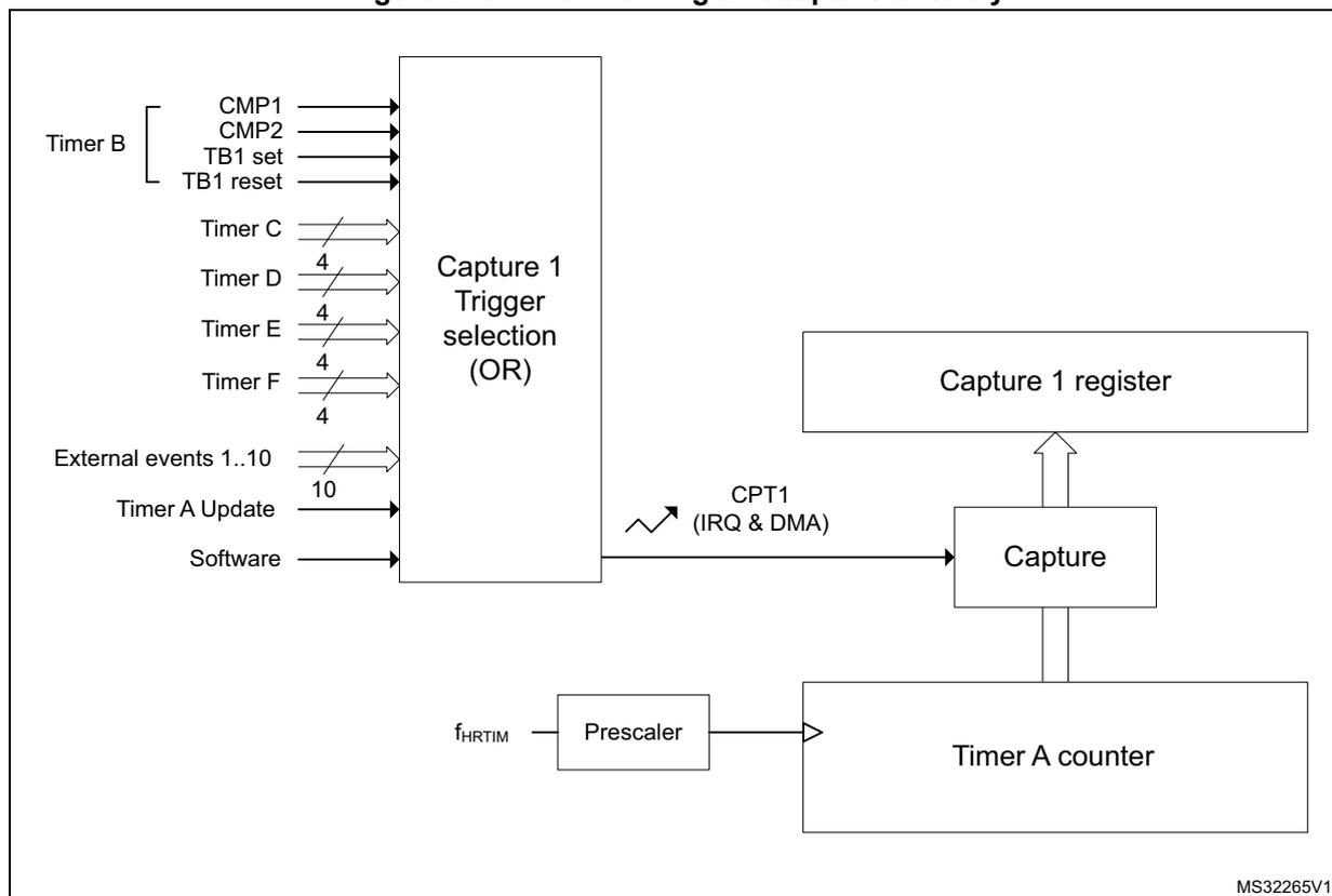
The diagram illustrates the capture circuitry for Timer A. On the left, various input signals are shown: Timer B (CMP1, CMP2, TB1 set, TB1 reset), Timer C, Timer D (4), Timer E (4), Timer F (4), External events 1..10 (10), Timer A Update, and Software. These inputs are connected to a block labeled 'Capture 1 Trigger selection (OR)'. The output of this block is labeled 'CPT1 (IRQ & DMA)' and is connected to a 'Capture' block. The 'Capture' block is also connected to a 'Capture 1 register' above it and a 'Timer A counter' below it. The 'Timer A counter' is connected to a 'Prescaler' block, which is in turn connected to the input \( f_{HRTIM} \) . The 'Capture' block has a bidirectional connection with the 'Capture 1 register' and a unidirectional connection with the 'Timer A counter'. The 'Timer A counter' has a unidirectional connection with the 'Capture' block. The 'Prescaler' block has a unidirectional connection with the 'Timer A counter'.
MS32265V1
Auto-delayed mode
This mode allows to have compare events generated relatively to capture events, so that for instance an output change can happen with a programmed timing following a capture. In this case, the compare match occurs independently from the timer counter value. It enables the generation of waveforms with timings synchronized to external events without the need of software computation and interrupt servicing.
As long as no capture is triggered, the content of the HRTIM_CMPxR register is ignored (no compare event is generated when the counter value matches the compare value). Once the capture is triggered, the compare value programmed in HRTIM_CMPxR is summed with the captured counter value in HRTIM_CPTxyR, and it updates the internal auto-delayed compare register, as seen on Figure 219. The auto-delayed compare register is internal to the timing unit and cannot be read. The HRTIM_CMPxR preload register is not modified after the calculation.
This feature is available only for compare 2 and compare 4 registers. compare 2 is associated with capture 1, while compare 4 is associated with capture 2. HRTIM_CMP2xR and HRTIM_CMP4xR compares cannot be programmed with a value below 3 \( f_{HRTIM} \) clock periods, as in the regular mode.
Figure 219. Auto-delayed overview (compare 2 only)
![Block diagram of the HRTIM auto-delayed compare mechanism for Compare 2. The diagram shows a Counter connected to Capture 1, Compare 2, Compare 1, and Compare 3. Capture 1 triggers an 'Add' block. The 'Add' block also receives input from Compare 2 and a 'Timeout feature if DELCMP2[1..0] = 1x' signal. The output of the 'Add' block is fed into 'Autodelayed Compare 2'. The output of 'Autodelayed Compare 2' is fed into a multiplexer (MUX) controlled by DELCMP2[1..0] bits. The MUX has two inputs: 00 and !00. The output of the MUX is fed into Compare 2. The diagram also shows the flow of data from the Counter to the Compare blocks and from the Compare blocks to the MUX.](/RM0440-STM32G4/24e7fd0de34b7184374166b3fdf6bad9_img.jpg)
The auto-delayed compare is only valid from the capture up to the period event: once the counter has reached the period value, the system is re-armed with compare disabled until a capture occurs.
DELCMP2[1:0] and DELCMP4[1:0] bits in HRTIM_TIMxCR register allow to configure the auto-delayed mode as follows:
• 00
Regular compare mode: HRTIM_CMP2xR and HRTIM_CMP4xR register contents are directly compared with the counter value.• 01
Auto-delayed mode: compare 2 and compare 4 values are recomputed and used for comparison with the counter after a capture 1/2 event.• 10 or 11
Auto-delayed mode with timeout: compare 2 and compare 4 values are recomputed and used for comparison with the counter after a capture 1/2 event or after a compare 1
match (DELCMPx[1:0]= 10) or a compare 3 match (DELCMPx[1:0]= 11) to have a timeout function if capture 1/2 event is missing.
When the capture occurs, the comparison is done with the (HRTIM_CMP2/4xR + HRTIM_CPT1/2xR) value. If no capture is triggered within the period, the behavior depends on the DELCMPx[1:0] value:
- • DELCMPx[1:0] = 01: the compare event is not generated
- • DELCMPx[1:0] = 10 or 11: the comparison is done with the sum of the 2 compares (for instance HRTIM_CMP2xR + HRTIM_CMP1xR). The captures are not taken into account if they are triggered after CMPx + CMP1 (resp. CMPx + CMP3).
The captures are enabled again at the beginning of the next PWM period.
If the result of the auto-delayed summation is above 0xFFFF (overflow), the value is ignored and no compare event is generated until a new period is started.
Note: DELCMPx[1:0] bitfield must be reset when reprogrammed from one value to the other to re-initialize properly the auto-delayed mechanism, for instance:
- • DELCMPx[1:0] = 10
- • DELCMPx[1:0] = 00
- • DELCMPx[1:0] = 11
As an example, Figure 220 shows how the following signal is generated:
- • Output set when the counter is equal to compare 1 value
- • Output reset 5 cycles after a falling edge on a given external event
Note: To simplify the figure, the high-resolution is not used in this example (CKPSC[2:0] = 101), thus the counter is incremented at the \( f_{HRTIM} \) rate. Similarly, the external event signal is shown without any resynchronization delay: practically, there is a delay of 1 to 2 \( f_{HRTIM} \) clock periods between the falling edge and the capture event due to an internal resynchronization stage which is necessary to process external input signals.
Figure 220. Auto-delayed compare
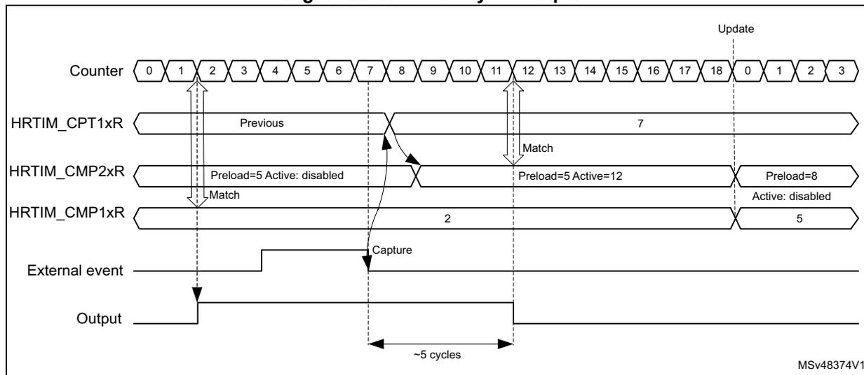
A regular compare channel (e.g. compare 1) is used for the output set: as soon as the counter matches the content of the compare register, the output goes to its active state.
A delayed compare is used for the output reset: the compare event can be generated only if a capture event has occurred. No event is generated when the counter matches the delayed compare value (counter = 4). Once the capture event has been triggered by the external event, the content of the capture register is summed to the delayed compare value to have the new compare value. In the example, the auto-delayed value 4 is summed to the capture equal to 7 to give a value of 12 in the auto-delayed compare register. From this time on, the compare event can be generated and happens when the counter is equal to 12, causing the output to be reset.
Overcapture management in auto-delayed mode
Overcapture is prevented when the auto-delayed mode is enabled (DELCMPx[1:0] = 01, 10, 11).
When multiple capture requests occur within the same counting period, only the first capture is taken into account to compute the auto-delayed compare value. A new capture is possible only:
- • Once the auto-delayed compare has matched the counter value (compare event)
- • Once the counter has rolled over (period)
- • Once the timer has been reset
Changing auto-delayed compare values
When the auto-delayed compare value is preloaded (PREEN bit set), the new compare value is taken into account on the next coming update event (for instance on the period event), regardless of when the compare register was written and if the capture occurred (see Figure 220 , where the delay is changed when the counter rolls over).
When the preload is disabled (PREEN bit reset), the new compare value is taken into account immediately, even if it is modified after the capture event has occurred, as per the example below:
- 1. At t1, DELCMP2 = 1.
- 2. At t2, CMP2_act = 0x40 => comparison disabled
- 3. At t3, a capture event occurs capturing the value CPTR1 = 0x20. => comparison enabled, compare value = 0x60
- 4. At t4, CMP2_act = 0x100 (before the counter reached value CPTR1 + 0x40) => comparison still enabled, new compare value = 0x120
- 5. At t5, the counter reaches the period value => comparison disabled, cmp2_act = 0x100
Similarly, if the CMP1(CMP3) value changes while DELCMPx = 10 or 11, and preload is disabled:
- 1. At t1, DELCMP2 = 2.
- 2. At t2, CMP2_act = 0x40 => comparison disabled
- 3. At t3, CMP3 event occurs - CMP3_act = 0x50 before capture 1 event occurs => comparison enabled, compare value = 0x90
- 4. At t4, CMP3_act = 0x100 (before the counter reached value 0x90) => comparison still enabled, compare 2 event occurs at = 0x140
Triggered-half mode
The purpose of this mode is to allow the synchronization of 2 interleaved converters that have variable frequency operation and require a 180° phase-shift. The basic principle is to
have a master-slave system. The slave converter synchronization is continuously adjusted based on the previous switching period of the master converter.
This is done using the capture unit. The switching period of the master converter is captured, divided by 2 and then stored in the compare 2 register by hardware. The compare 2 register contains a value equal to half of the captured period, which is the master converter switching period. The compare 2 event can then be used to trigger a second timing unit that manages the slave converter.
This mode is enabled by setting the TRGH LF bit in the HRTIM_TIMxCR2 register. This bit cannot be changed once the timer is operating (TxEN bit set).
The triggered-half mode must not be used simultaneously with other modes using CMP2 (dual channel dac trigger, interleaved and balanced idle modes).
The initial value CMP2 can be written by the user, but is ignored once the first capture is triggered. The preload mechanism is disabled for CMP2 when the TRGH LF bit is reset.
Figure 221. Triggered-half mode example
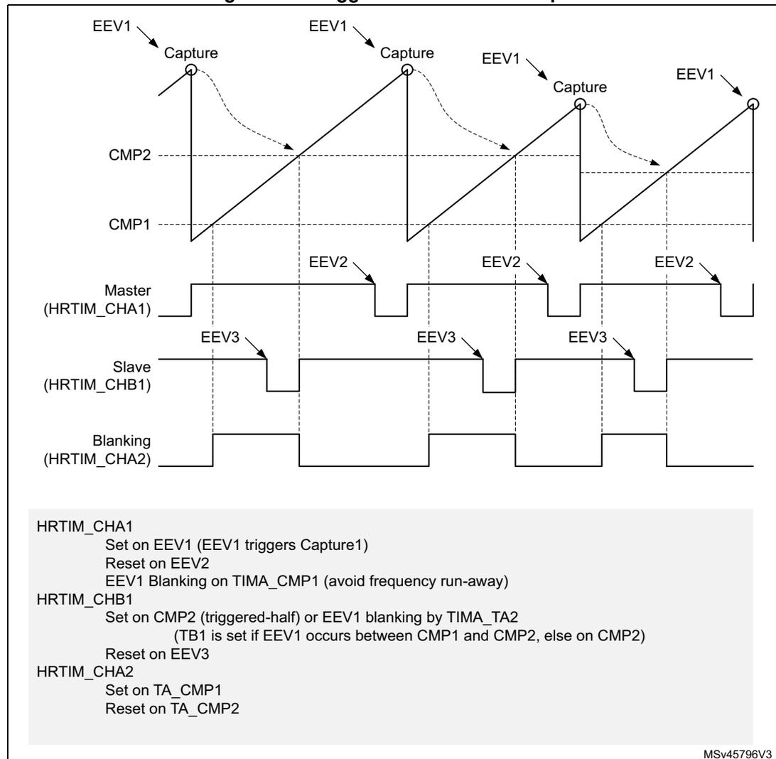
HRTIM_CHA1
Set on EEV1 (EEV1 triggers Capture1)
Reset on EEV2
EEV1 Blanking on TIMA_CMP1 (avoid frequency run-away)
HRTIM_CHB1
Set on CMP2 (triggered-half) or EEV1 blanking by TIMA_TA2
(TB1 is set if EEV1 occurs between CMP1 and CMP2, else on CMP2)
Reset on EEV3
HRTIM_CHA2
Set on TA_CMP1
Reset on TA_CMP2
MSv45796V3
Note: In triggered half mode, the compare2 register is controlled by hardware and writing it has no effect. However the written value is stored in the preload register and becomes active on the update event following the exit of this mode.
Push-pull mode
This mode primarily aims at driving converters using push-pull topologies. It also needs to be enabled when the delayed idle protection is required, typically for resonant converters (refer to Section 28.3.10: Delayed protection ).
The push-pull mode is enabled by setting PSHPLL bit in the HRTIM_TIMxCR register.
It applies the signals generated by the crossbar to output 1 and output 2 alternatively, on the period basis, maintaining the other output to its inactive state. The redirection rate (push-pull frequency) is defined by the timer's period event, as shown on Figure 222 . The push-pull period is twice the timer counting period.
Figure 222. Push-pull mode block diagram
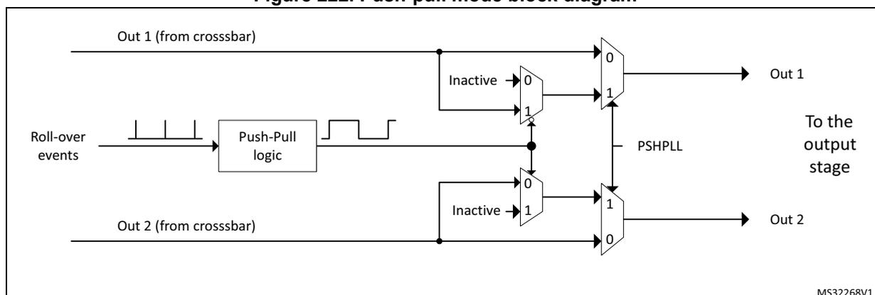
The push-pull mode is available when the timer operates in continuous mode and in single-shot mode. It is necessary to disable the timer to stop a push-pull operation and to reset the counter before re-enabling it.
To get a correct behavior, the event selected as source of the counter reset must be also selected for setting (or resetting) the output. It must set the output if the output is set on period, else it must reset it. If it is not done, the output switching from its inactive period to its active period may be incorrect (may unexpectedly rise or may unexpectedly stay low).
The signal shape is defined using HRTIM_SETxyR and HRTIM_RSTxyR for both outputs. It is necessary to have HRTIM_SETx1R = HRTIM_SETx2R and HRTIM_RSTx1R = HRTIM_RSTx2R to have both outputs with identical waveforms and to achieve a balanced operation. Still, it is possible to have different programming on both outputs for other uses.
The CPPSAT status bit in HRTIM_TIMxISR indicates on which output the signal is currently active. CPPSTAT is reset when the push-pull mode is disabled.
In the example given on Figure 223 , the timer internal waveform is defined as follows:
- • Output set on period event
- • Output reset on compare 1 match event
Figure 223. Push-pull mode example
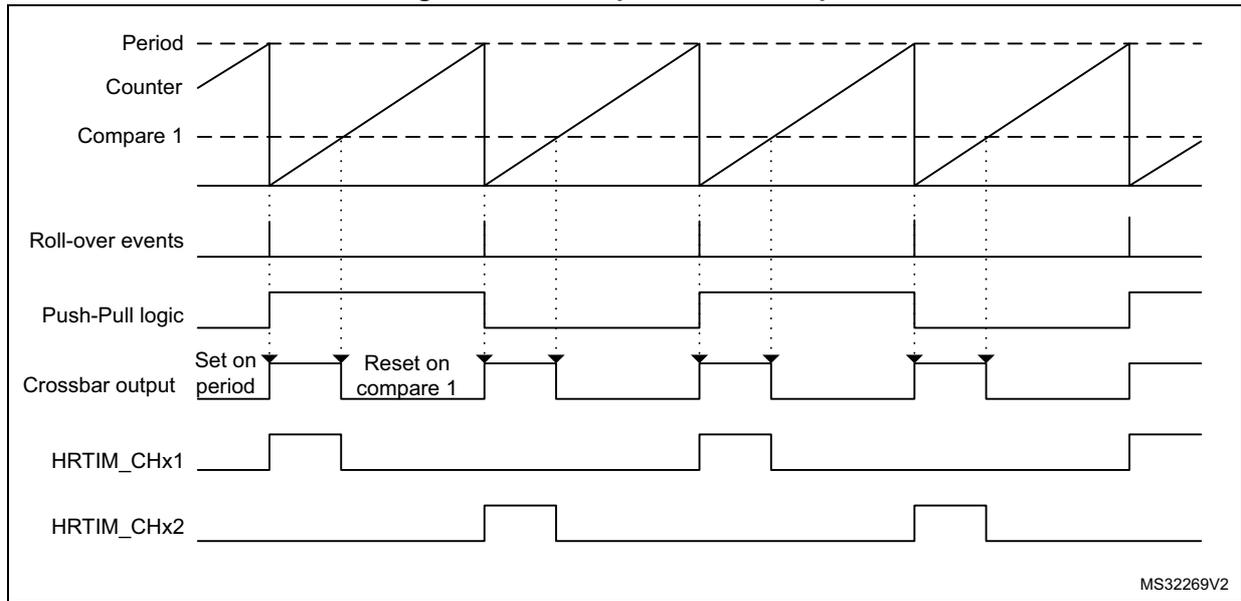
The diagram illustrates the following signals:
- Period : The maximum value of the counter.
- Counter : A sawtooth waveform ramping from zero to the Period.
- Compare 1 : A threshold level for resetting the output.
- Roll-over events : Pulses occurring when the counter reaches the Period.
- Push-Pull logic : A square wave that toggles on every roll-over event.
- Crossbar output : A signal that is Set on period and Reset on compare 1 .
- HRTIM_CHx1 : Output signal active during the first phase of the push-pull cycle.
- HRTIM_CHx2 : Output signal active during the second phase of the push-pull cycle.
MS32269V2
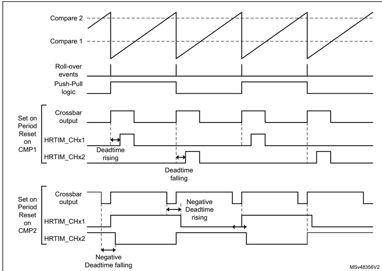
Figure 224 shows how the deadtime is inserted in push-pull mode, for both positive and negative deadtimes. In this case, the outputs are not complemented any more, and the deadtime is applied on each output individually (both output 1 and output 2 of the crossbar are used).
Figure 224. Push-pull with deadtime
Deadtime
A deadtime insertion unit allows to generate a couple of complementary signals from a single reference waveform, with programmable delays between active state transitions. This is commonly used for topologies using half-bridges or full bridges. It simplifies the software: only 1 waveform is programmed and controlled to drive two outputs.
The Dead time insertion is enabled by setting DTEN bit in HRTIM_OUTxR register. The complementary signals are built based on the reference waveform defined for output 1, using HRTIM_SETx1R and HRTIM_RSTx1R registers: HRTIM_SETx2R and HRTIM_RSTx2R registers are not significant when DTEN bit is set.
Two deadtimes can be defined in relationship with the rising edge and the falling edge of the reference waveform, as in Figure 225 .
Figure 225. Complementary outputs with deadtime insertion
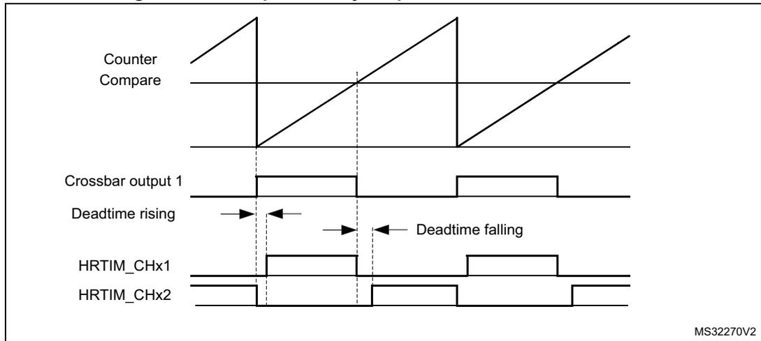
Timing diagram showing complementary outputs with deadtime insertion. The diagram includes five waveforms: Counter Compare (a sawtooth wave), Crossbar output 1 (a square wave), Deadtime rising (indicated by a right arrow), Deadtime falling (indicated by a left arrow), and HRTIM_CHx1 and HRTIM_CHx2 (complementary square waves). The deadtime is shown as the time interval between the falling edge of one output and the rising edge of the other.
MS32270V2
Negative deadtime values can be defined when some control overlap is required. This is done using the deadtime sign bits (SDTFx and SDTRx bits in HRTIM_DTxR register).
Figure 226 shows complementary signal waveforms depending on respective signs.
Figure 226. Deadtime insertion versus deadtime sign (1 indicates negative deadtime)
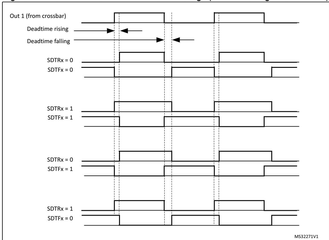
Timing diagram showing deadtime insertion versus deadtime sign. The diagram includes five waveforms: Out 1 (from crossbar), Deadtime rising (indicated by a right arrow), Deadtime falling (indicated by a left arrow), and four pairs of complementary square waves (HRTIM_CHx1 and HRTIM_CHx2) corresponding to different deadtime sign settings: SDTRx = 0, SDTFx = 0; SDTRx = 1, SDTFx = 1; SDTRx = 0, SDTFx = 1; and SDTRx = 1, SDTFx = 0. The deadtime is shown as the time interval between the falling edge of one output and the rising edge of the other.
MS32271V1
The deadtime values are defined with DTFx[8:0] and DTRx[8:0] bitfields and based on a specific clock prescaled according to DTPRSC[2:0] bits, as follows:
where x is either R or F and \( t_{DTG} = (2^{(DTPRSC[2:0])}) \times (t_{HRTIM} / 8) \) .
Table 237 gives the resolution and maximum absolute values depending on the prescaler value.
Table 237. Deadtime resolution and max absolute values
| DTPRSC[2:0] | \( t_{DTG} \) | \( t_{DTx} \) max | \( f_{HRTIM} = 170 \text{ MHz} \) | |
|---|---|---|---|---|
| \( t_{DTG} \) (ns) | \( |t_{DTx}| \) max ( \( \mu\text{s} \) ) | |||
| 000 | \( t_{HRTIM} / 8 \) | \( 511 * t_{DTG} \) | 0.73 | 0.38 |
| 001 | \( t_{HRTIM} / 4 \) | 1.47 | 0.75 | |
| 010 | \( t_{HRTIM} / 2 \) | 2.94 | 1.50 | |
| 011 | \( t_{HRTIM} \) | 5.89 | 3.01 | |
| 100 | \( 2 * t_{HRTIM} \) | 11.76 | 6.01 | |
| 101 | \( 4 * t_{HRTIM} \) | 23.53 | 12.03 | |
| 110 | \( 8 * t_{HRTIM} \) | 47.06 | 24.04 | |
| 111 | \( 16 * t_{HRTIM} \) | 94.12 | 48.10 | |
Figure 227 to Figure 230 present how the deadtime generator behaves for reference waveforms with pulsewidth below the deadtime values, for all deadtime configurations.
Figure 227. Complementary outputs for low pulsewidth (SDTRx = SDTFx = 0)
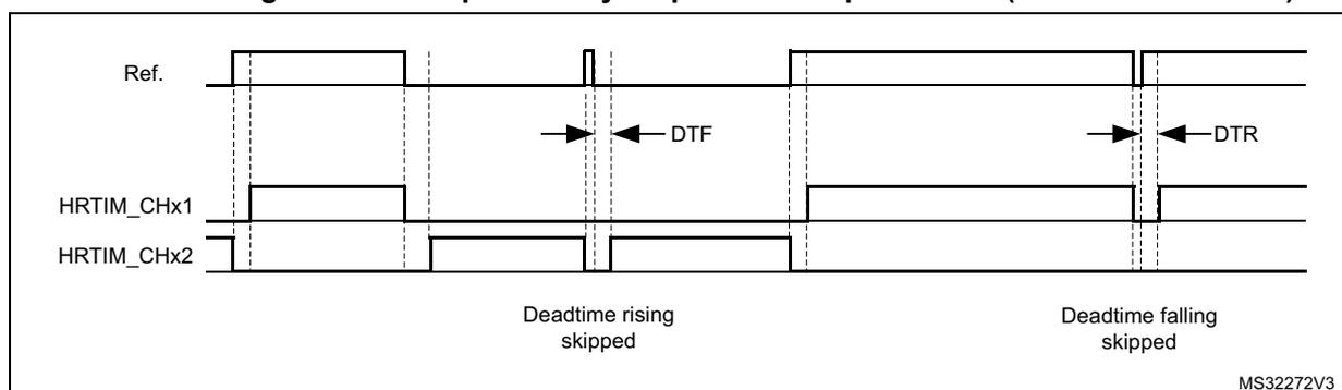
Figure 228. Complementary outputs for low pulsewidth (SDTRx = SDTFx = 1)
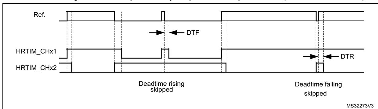
Figure 229. Complementary outputs for low pulsewidth (SDTRx = 0, SDTFx = 1)
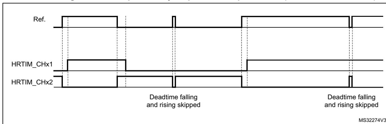
Figure 230. Complementary outputs for low pulsewidth (SDTRx = 1, SDTFx=0)
For safety purposes, it is possible to prevent any spurious write into the deadtime registers by locking the sign and/or the value of the deadtime using DTFLKx, DTRLKx, DTFSLKx and DTRSLKx. Once these bits are set, the related bits and bitfields are becoming read only until the next system reset.
Caution: DTEN bit must not be changed in the following cases:
- - When the timer is enabled (TxEN bit set)
- - When the timer outputs are set/reset by another timer (while TxEN is reset)
Otherwise, an unpredictable behavior would result.
It is therefore necessary to disable the timer (TxCEN bit reset) and have the corresponding outputs disabled.
For the particular case where DTEN must be set while the burst mode is enabled with a deadtime upon entry (BME = 1, DIDL = 1, IDLEM = 1), it is necessary to force the two outputs in their IDLES state by software commands (SST, RST bits) before setting DTEN bit. This is to avoid any side effect resulting from a burst mode entry that would happen immediately before a deadtime enable.
28.3.5 Master timer
The main purpose of the master timer is to provide common signals to the 6 timing units, either for synchronization purpose or to set/reset outputs. It does not have direct control over any outputs, but still can be used indirectly by the set/reset crossbars.
Figure 231 provides an overview of the master timer.
Figure 231. Master timer overview
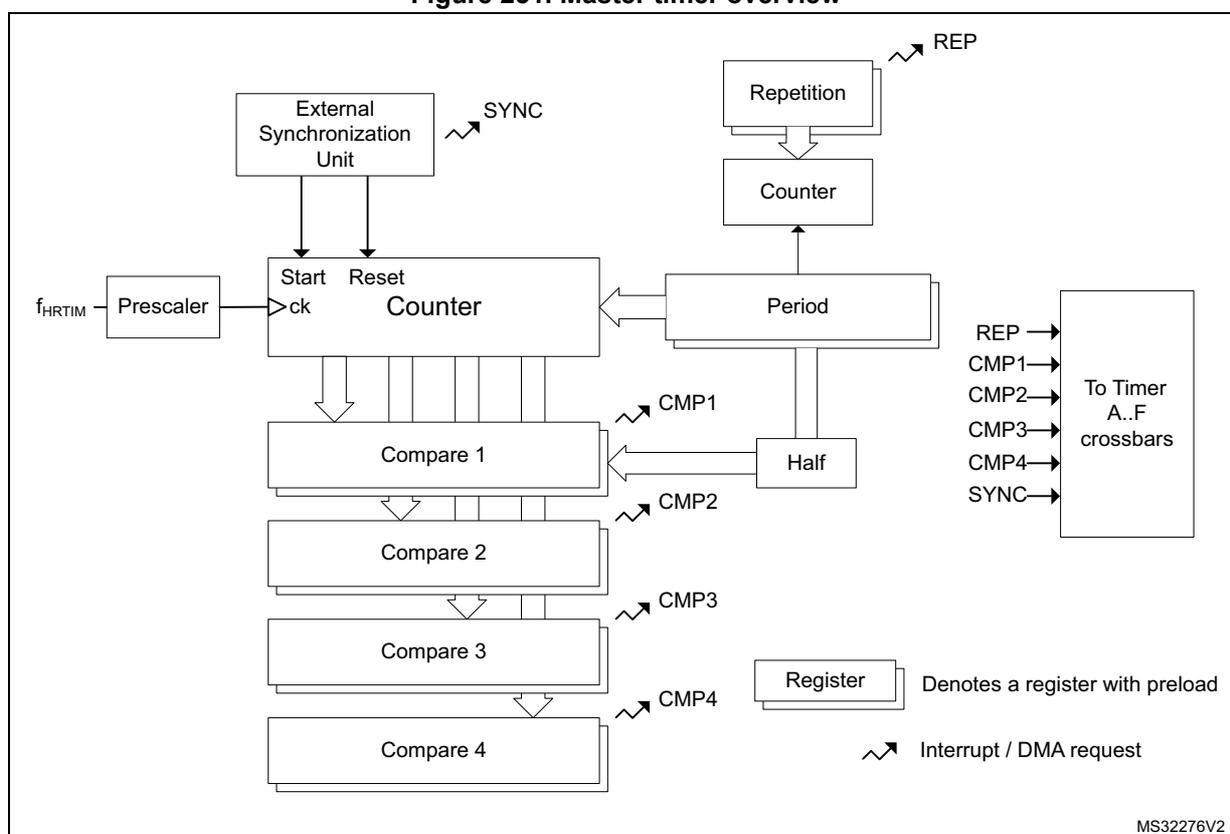
The diagram illustrates the internal architecture of the master timer. At the top left, an external clock signal \( f_{HRTIM} \) is divided by a Prescaler to provide a clock (ck) to the Counter. The Counter is also controlled by Start and Reset signals from an External Synchronization Unit, which outputs a SYNC signal. The Counter's output is connected to a Period register and a Half register. The Period register is connected to a Repetition unit, which outputs a REP signal, and also to a 'To Timer A..F crossbars' block. The Half register is connected to the same crossbars block. The Counter's output is also connected to four Compare units (Compare 1, Compare 2, Compare 3, and Compare 4). Each Compare unit has a corresponding Compare register (CMP1, CMP2, CMP3, CMP4) and outputs a compare signal (CMP1, CMP2, CMP3, CMP4) to the crossbars block. A Register unit, which denotes a register with preload, is connected to the Counter and outputs an Interrupt / DMA request signal. The crossbars block on the right receives inputs from the Repetition unit, the Period register, the Half register, the Compare units, and the Register unit, and outputs signals to the Timer A..F crossbars.
The master timer is based on the very same architecture as the timing units, with the following differences:
- • It does not have outputs associated with, nor output related control
- • It does not have its own crossbar unit, nor push-pull or deadtime mode
- • It can only be reset by the external synchronization circuitry
- • It does not have a capture unit, nor the auto-delayed mode
- • It does not include external event blanking and windowing circuitry
- • It has a limited set of interrupt / DMA requests: compare 1..4, repetition, register update and external synchronization event.
The master timer control register includes all the timer enable bits, for the master and timer A..F timing units. This allows to have all timer synchronously started with a single write access.
It also handles the external synchronization for the whole HRTIM timer (see Section 28.3.19: Synchronizing the HRTIM with other timers or HRTIM instances ), with both MCU internal and external (inputs/outputs) resources.
Master timer control registers are mapped with the same offset as the timing units' registers.
28.3.6 Up-down counting mode
The HRTIM is natively designed with up-counters. It offers however an operating mode with up-down counters, also called center-aligned mode.
This mode is enabled using the UDM bit in the HRTIM_TIMxCR2 register. This bit must not be changed once the timer is operating (TxEN bit set). It is only available for the TIMA..F. The master timer only works in up-counting mode.
Not all HRTIM features are supported in up-down counting. This section details the functional differences versus up-counting mode.
The period in HRTIM_PERxR must be preloaded (or static) in up-down mode. It can be updated only on period event or on counter reset.
The set/reset crossbar programming differs as follows:
The events coming from the timing units are setting/resetting the outputs depending on the counter up/down direction:
- • If the event is enabled in the HRTIM_SETxyR register, it sets the output during up-counting and reset it during down-counting.
- • If the event is enabled in the HRTIM_RSTxyR register, it resets the output during up-counting and set it during down-counting.
- • If the events are enabled both in HRTIM_SETxyR and HRTIM_RSTxyR registers, the output toggles.
This applies to :
- – The timing unit: period, compare 1..4, register update (6 events)
- – The master timer: period, compare 1..4, HRTIM synchronization (6 events)
- – All other timing units (e.g. timer B..F for timer A): TIMEVNT1..9 (9 events described in Table 234 )
The Figure 232 below shows how to generate basic waveforms.
Figure 232. Basic symmetric waveform in up-down counting mode
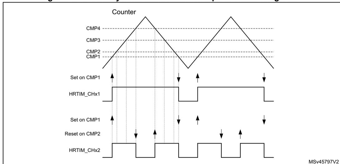
The figure is a timing diagram illustrating basic symmetric waveforms in up-down counting mode. At the top, the 'Counter' is shown as a sawtooth waveform that ramps up and then down. Four horizontal dashed lines represent comparison levels: CMP4 (highest), CMP3, CMP2, and CMP1 (lowest). Below the counter, two output waveforms are shown: HRTIM_CHx1 and HRTIM_CHx2. HRTIM_CHx1 is initially low. It transitions to high when the counter is up-counting and reaches the CMP1 level ('Set on CMP1'). It transitions back to low when the counter is down-counting and reaches the CMP1 level ('Set on CMP1'). HRTIM_CHx2 is initially low. It transitions to high when the counter is up-counting and reaches the CMP1 level ('Set on CMP1'). It transitions back to low when the counter is down-counting and reaches the CMP2 level ('Reset on CMP2'). Vertical dashed lines connect the counter's comparison points to the output transitions. The diagram is labeled 'MSv45797V2' in the bottom right corner.
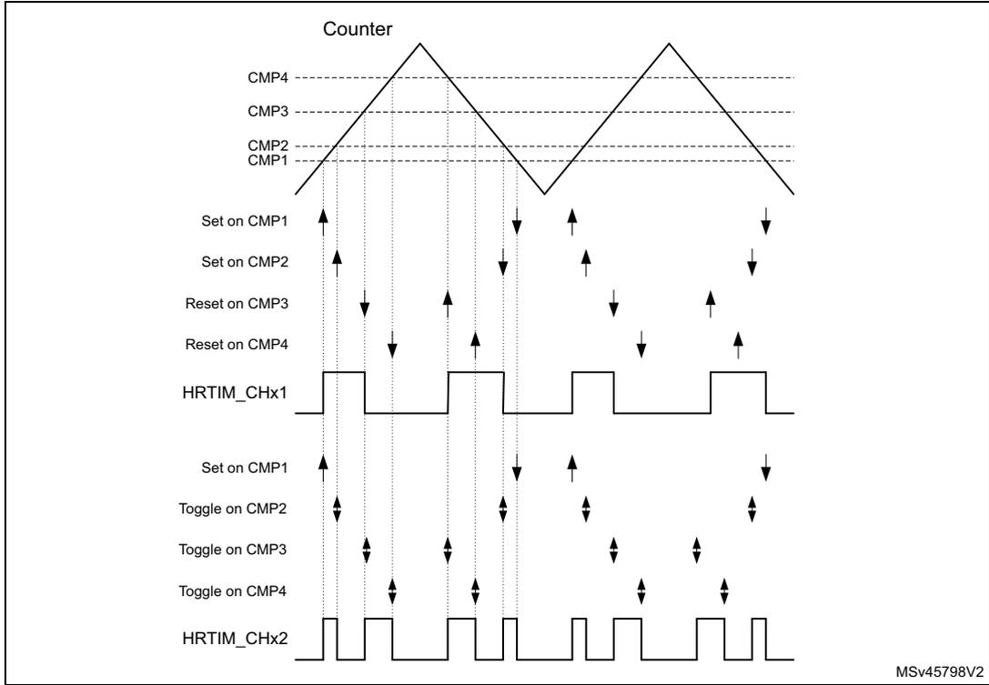
The Figure 233 below shows how to generate some more complex waveforms, using the 4 available compare units and the toggle mode.
Figure 233. Complex symmetric waveform in up-down counting mode
The Figure 234 shows how to generate an asymmetric waveform. In this case, it must be noticed that it is necessary to have compare 2 value greater than compare 1 value for the waveform to be asymmetric.
Figure 234. Asymmetric waveform in up-down counting mode
Note: For asymmetric operation, it is required that \( CMP2 > CMP1 \) .
The behavior of the software forcing bits and external events EXTEVNT1..10 is identical for up-only and up-down counting mode. The Figure 235 below shows how a pulse can be shorted in response to external events.
Figure 235. External event management in up-down counting mode
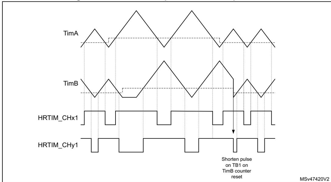
The up-down counting mode is available for both continuous and single-shot (retriggerable and non-retriggerable) operating modes. A reset causes the counter to re-start from 0. The Figure 236 below shows the counter behavior in single-shot retriggerable mode, for TimB.
Figure 236. Interleaved up-down counter operation
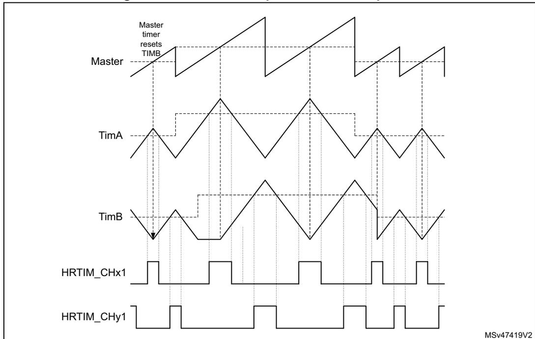
Figure 237. Interleaved up-down counter operation
In up-down counting mode, the compare values must be 3 periods of the \( f_{HRTIM} \) clock below the period value ( \( TIMx\_PER - 0xC0 \) if \( CKPSC[2:0] = 0 \) , \( TIMx\_PER - 0x60 \) if \( CKPSC[2:0] = 1 \) , \( TIMx\_PER - 0x30 \) if \( CKPSC[2:0] = 2, \dots \) ). This applies for the compare events generated inside the timing unit. For compare events generated in other timing units, it is mandatory to avoid any event occurring within less than 1 period of the \( f_{HRTIM} \) clock of a counter direction change (counter at 0, period event or counter reset).
The following features are supported in up-down counting mode:
- – Half mode
- – Deadtime insertion
- – Push-pull mode, alternance push-pull done on when counter = 0 (see Figure 238 ).
- – Delayed Idle
- – Burst mode
- – PWM mode with “greater than” comparison (see Figure 239 ).
Figure 238. Push-pull up-down mode example
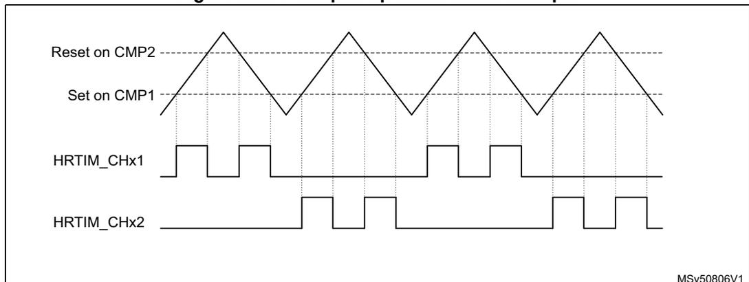
Figure 239. Up-down mode with “greater than” comparison
Caution: The following features are not supported in up-down counting mode:
- – Auto-delayed mode
- – Balanced Idle
- – Triggered-half mode
The capture function is supported with the following differences:
- – the capture value is referred to counting start, when up-counting
- – the capture value is referred to the PER event when down counting
- – the bit 16 of the capture register holds the counting direction status
The counter roll-over event is defined differently in up-down counting mode to support various operating condition. It can be either generated:
- – when the counter is equal to 0 (“valley” mode)
- – when the counter reaches the period value set in the HRTIM_PERxR (“crest” mode)
- – when both conditions are met (either 0 or HRTIM_PERxR value)
This event is used for multiple purposes in the HRTIM. The generation mode (valley, crest or both) can be programmed individually depending on the destination. Table 238 summarizes the use cases and associated roll-over mode (xxROM[1:0]) programming bits in the HRTIM_TIMxCR2 register.
Table 238. Roll-over event destination and mode programming
| Roll-over event use | Programming bits |
|---|---|
| Output set/reset | OUTROM[1:0] |
| Register content update trigger (transfer from preload to active) | ROM[1:0] |
| IRQ and/or DMA request trigger | ROM[1:0] |
| Burst mode clock source and /or burst start trigger | BMROM[1:0] |
| ADC trigger (see Section : ADC post-scaler for details) | ADROM[1:0] |
| External event filtering | ROM[1:0] |
| Repetition counter decrement | ROM[1:0] |
| Fault and event counter | FEROM[1:0] |
Note: For events where both reset and roll-over are considered (IRQ/DMA and TxRSTU), the ROM[1:0] only influences the roll-over generation. The reset event is always taken into account whatever the ROM[1:0] value.
The roll-over event generation is defined as per following xxROM[1:0] bitfield setting:
- • xxROM[1:0] = 00: event generated when both conditions are met (either 0 or HRTIM_PERxR value)
- • xxROM[1:0] = 01: event generated when the counter is equal to 0 (“valley” mode) or when the counter is reset
- • xxROM[1:0] = 10: event generated when the counter reaches the period value set in the HRTIM_PERxR (“crest” mode)
Figure 240 here-below shows a push-pull up-down mode with set on period event and OUTROM[1:0] =10.
Figure 240. Up-down mode with output set on period event, for OUTROM[1:0]=10
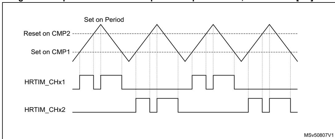
The timing diagram illustrates the operation of an HRTIM timer in up-down mode. The top waveform shows the counter value over time, forming a triangular wave. Key events are marked: 'Set on Period' at the peaks (crest mode) and 'Reset on CMP2' at the valleys. Below the counter waveform, two output signals are shown: HRTIM_CHx1 and HRTIM_CHx2. HRTIM_CHx1 is a square wave that toggles its state at each 'Set on Period' event. HRTIM_CHx2 is a square wave that toggles its state at each 'Reset on CMP2' event. Vertical dashed lines connect the events on the counter waveform to the corresponding transitions on the output signals. The diagram is labeled with 'MSv50807V1' in the bottom right corner.
Figure 241 below shows how the repetition counter is decremented in up-down counting mode.
Figure 241. Repetition counter behavior in up-down counting mode
![Timing diagram showing Counter, REP, and ROM[1:0] signals over time. The Counter signal is a sawtooth wave. The REP signal is high when the Counter is at its peak. The ROM[1:0] signal is a 2-bit bus that changes its value based on the REP signal. The diagram shows six rows of signals. The first row shows Counter, REP = 0, ROM[1:0] = 00. The second row shows Counter, REP = 0, ROM[1:0] = 01. The third row shows Counter, REP = 0, ROM[1:0] = 10. The fourth row shows Counter, REP = 1, ROM[1:0] = 01. The fifth row shows Counter, REP = 1, ROM[1:0] = 10. The sixth row shows Counter, REP = 2, ROM[1:0] = 00. The diagram illustrates that the repetition counter is decremented in up-down counting mode.](/RM0440-STM32G4/9a14059138e1571ec5e366e20bc83ac0_img.jpg)
The dual channel DAC triggers are working as for the up-counting mode.
The event blanking and windowing differs so as to have the blanking or windowing done within the output pulse, at a programmable time. The EExFLTR[3:0] codes are depending on the UDM bit setting, as per the Table 239 below. Whenever the roll-over event is used for blanking or windowing, the ROM[1:0] programming applies for defining when it is generated.
Table 239. EExFLTR[3:0] codes depending on UDM bit setting
| EE1FLTR[3:0] | Up-counting mode (UDM = 0) | Up/down-counting mode (UDM = 1) |
|---|---|---|
| 0010 | Blanking from counter reset/roll-over to compare 2 | Blanking from compare 1 to compare 2, only during the up-counting phase |
| 0100 | Blanking from counter reset/roll-over to compare 4 | Blanking from compare 3 to compare 4, only during the up-counting phase |
| 1101 | Windowing from counter reset/roll-over to compare 2 | Windowing from compare 2 to compare 3, only during the up-counting phase |
| 1110 | Windowing from counter reset/roll-over to compare 3 | Windowing from compare 2 to compare 3, only during the down-counting phase |
| 1111 | Windowing from another timing unit: TIMWIN source (see Table 243 for details) | Windowing from compare 2 during the up-counting phase to compare 3 during the down-counting phase |
28.3.7 Set / reset events priorities and narrow pulses management
This section describes how the output waveform is generated when several set and/or reset requests are occurring within 3 consecutive \( t_{HRTIM} \) periods.
Case 1: clock prescaler CKPSC[2:0] < 5
An arbitration is performed during each \( t_{HRTIM} \) period, in 3 steps:
- 1. For each active event, the desired output transition is determined (set, reset or toggle).
- 2. A predefined arbitration is performed among the active events (from highest to lowest priority CMP4 → CMP3 → CMP2 → CMP1 → PER, see Section : Concurrent set requests/ Concurrent reset requests ).
- 3. A high-resolution delay-based arbitration is performed with reset having the highest priority, among the low-resolution events and events having won the predefined arbitration.
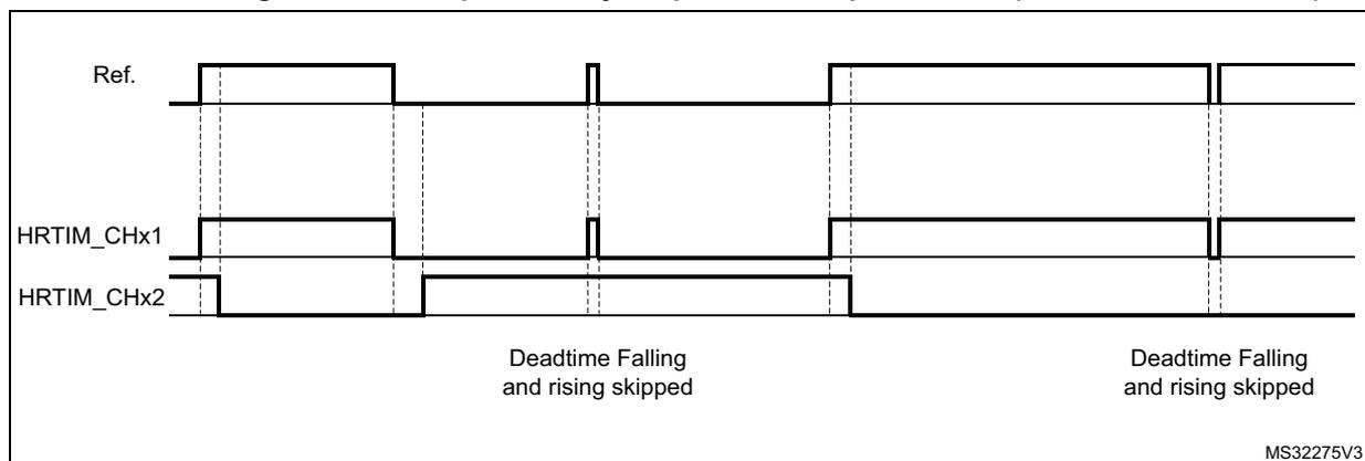
When set and reset requests from two different sources are simultaneous, the reset action has the highest priority. If the interval between set and reset requests is below 2 \( t_{HRTIM} \) period, the behavior depends on the time interval and on the alignment with the \( f_{HRTIM} \) clock, as shown on Figure 242 .
- Note:
- If the set and reset requests are simultaneous and coming from the same timing unit, the CMPx priority applies, as shown in step 2 here-above. For instance, taking CMP2 = CMP4:
- - If CMP2 does a set and CMP4 a reset, the output is reset.
- - If CMP2 does a reset and CMP4 a set, the output is set.
Figure 242. Short distance set/reset management for narrow pulse generation
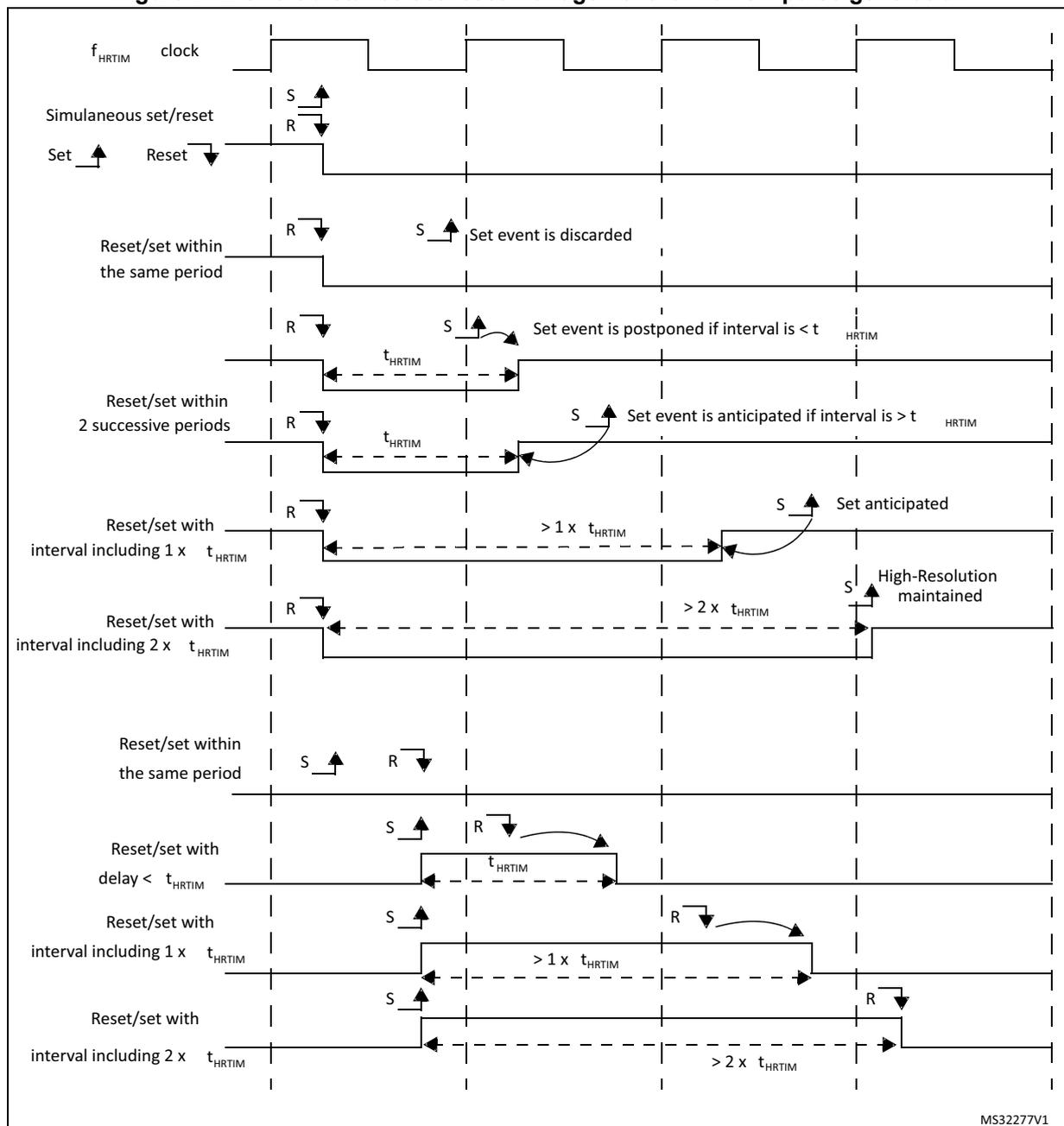
The diagram illustrates the timing relationships between the \( f_{HRTIM} \) clock and set (S) and reset (R) events for narrow pulse generation. The clock is a periodic square wave. The diagram is divided into several horizontal sections, each showing a different scenario:
- Simultaneous set/reset: Both S and R events occur at the same time. The output pulse is ignored.
- Set then Reset within the same period: A set event (S) is followed by a reset event (R) within the same \( t_{HRTIM} \) period. The output pulse is ignored.
- Reset then Set within the same period: A reset event (R) is followed by a set event (S) within the same \( t_{HRTIM} \) period. The set event is discarded.
- Reset then Set within 2 successive periods (interval \( < t_{HRTIM} \) ): A reset event (R) is followed by a set event (S) across two periods, with an interval less than \( t_{HRTIM} \) . The set event is postponed until the start of the next period.
- Reset then Set within 2 successive periods (interval \( > t_{HRTIM} \) ): A reset event (R) is followed by a set event (S) across two periods, with an interval greater than \( t_{HRTIM} \) . The set event is anticipated and occurs before the start of the next period.
- Reset then Set with interval including 1 \( t_{HRTIM} \) : A reset event (R) is followed by a set event (S) with an interval of approximately one \( t_{HRTIM} \) period. The set event is anticipated.
- Reset then Set with interval including 2 \( t_{HRTIM} \) : A reset event (R) is followed by a set event (S) with an interval of approximately two \( t_{HRTIM} \) periods. The set event is anticipated, and high-resolution is maintained.
- Set then Reset within the same period: A set event (S) is followed by a reset event (R) within the same \( t_{HRTIM} \) period. A pulse of one \( t_{HRTIM} \) period is generated.
- Set then Reset with delay \( < t_{HRTIM} \) : A set event (S) is followed by a reset event (R) with a delay less than \( t_{HRTIM} \) . A pulse of one \( t_{HRTIM} \) period is generated.
- Set then Reset with interval including 1 \( t_{HRTIM} \) : A set event (S) is followed by a reset event (R) with an interval of approximately one \( t_{HRTIM} \) period. A pulse of one \( t_{HRTIM} \) period is generated.
- Set then Reset with interval including 2 \( t_{HRTIM} \) : A set event (S) is followed by a reset event (R) with an interval of approximately two \( t_{HRTIM} \) periods. A pulse of two \( t_{HRTIM} \) periods is generated.
MS32277V1
If the set and reset events are generated within the same \( t_{HRTIM} \) period, the reset event has the highest priority and the set event is ignored.
If the set and reset events are generated with an interval below \( t_{HRTIM} \) period, across 2 periods, a pulse of 1 \( t_{HRTIM} \) period is generated.
If the set and reset events are generated with an interval below 2 \( t_{HRTIM} \) periods, a pulse of 2 \( t_{HRTIM} \) periods is generated.
If the set and reset events are generated with an interval between 2 and 3 \( t_{HRTIM} \) periods, the high-resolution is available if the interval is over 2 complete \( t_{HRTIM} \) periods.
If the set and reset events are generated with an interval above 3 \( t_{HRTIM} \) periods, the high-resolution is always available.
Concurrent set requests/ Concurrent reset requests
When multiple sources are selected for a set event, an arbitration is performed when the set requests occur within the same \( f_{HRTIM} \) clock period.
In case of multiple requests from adjacent timers (TIMEVNT1..9), the request which occurs first is taken into account. The arbitration is done in 2 steps, depending on:
- 1. the source (CMP4 → CMP3 → CMP2 → CMP1),
- 2. the delay.
If multiple requests from the master timer occur within the same \( f_{HRTIM} \) clock period, a predefined arbitration is applied and a single request is taken into account, whatever the effective high-resolution setting (from the highest to the lowest priority):
MSTCMP4 → MSTCMP3 → MSTCMP2 → MSTCMP1 → MSTCMPER
Note: It is advised to avoid generating multiple set (reset) requests from the master timer to a given timer with an interval below 3x \( t_{HRTIM} \) to maintain the high-resolution.
When multiple requests internal to the timer occur within the same \( f_{HRTIM} \) clock period, a predefined arbitration is applied and the requests are taken with the following priority, whatever the effective timing (from highest to lowest):
CMP4 → CMP3 → CMP2 → CMP1 → PER
Note: Practically, this is of a primary importance when multiple compare events can be simultaneously generated or when using auto-delayed compare 2 and compare 4 simultaneously (i.e. when the effective set/reset cannot be determined a priori because it is related to an external event). In this case, the highest priority signal must be affected to the CMP4 event.
Last, the highest priority is given to low-resolution events: EXTEVNT1..10, RESYNC (coming from SYNC event if SYNCRSTx or SYNCSTRTx is set or from a software reset), update and software set (SST). The update event is considered as having the largest delay (0x1F if PSC = 0).
As a summary, in case of a close vicinity (events occurring within the same \( f_{HRTIM} \) clock period), the effective set (reset) event is arbitrated between:
- • Any TIMEVNT1..9 event
- • A single source from the master (as per the fixed arbitration given above)
- • A single source from the timer
- • The “low-resolution events”.
The same arbitration principle applies for concurrent reset requests. In this case, the reset request has the highest priority.
Case 2: clock prescaler CKPSC[2:0] ≥ 5
The narrow pulse management is simplified when the high-resolution is not effective.
A set or reset event occurring within the prescaler clock cycle is delayed to the next active edge of the prescaled clock (as for a counter reset), even if the arbitration is still performed every \( t_{HRTIM} \) cycle.
If a reset event is followed by a set event within the same prescaler clock cycle, the latest event is considered.
28.3.8 External events global conditioning
The HRTIM timer can handle events not generated within the timer, referred to as “external event”. These external events come from multiple sources, either on-chip or off-chip:
- • built-in comparators,
- • digital input pins (typically connected to off-chip comparators and zero-crossing detectors),
- • on-chip events for other peripheral (ADC’s analog watchdogs and general purpose timer trigger outputs).
The external events conditioning circuitry allows to select the signal source for a given channel (with a 4:1 multiplexer) and to convert it into an information that can be processed by the crossbar unit (for instance, to have an output reset triggered by a falling edge detection on an external event channel).
Up to 10 external event channels can be conditioned and are available simultaneously for any of the 6 timers. This conditioning is common to all timers, since this is usually dictated by external components (such as a zero-crossing detector) and environmental conditions (typically the filter set-up is related to the applications noise level and signature). Figure 243 presents an overview of the conditioning logic for a single channel.
Figure 243. External event conditioning overview (1 channel represented)
![Figure 243. External event conditioning overview (1 channel represented). The diagram shows the signal flow for a single external event channel (EEVx). It starts with 'hrtim_eevx[4:1]' inputs being multiplexed by 'EExSRC[1:0]'. The output goes to 'EEVx_muxout (to FAULT circuitry)' and also through 'Edge and polarity' logic (inverters and AND gates) controlled by 'EExPOL' and 'EExSNS[1:0]'. The signal then passes through a 'Digital Filter' (labeled 'Filtering (EEV6..10 only)') controlled by 'EExF[3:0]' and 'Prescaler' (labeled 'Prescaler (EEV6..10 only)') controlled by 'EExSD[1:0]'. The filtered signal enters a 'Fast asynchronous path' (labeled 'Fast path (EEV1..5 only)') controlled by 'EExFAST'. This path leads to 'Timer A..F' and 'Output stage'. A 'Synchronous path' (labeled 'Synchronous path EExFAST = 0') also connects the 'Timer A..F' to the 'Output stage'. 'Other EEVNT channels' (labeled '9') are also connected to 'Timer A..F'. The diagram is divided into four sections: 'Source selection', 'Edge and polarity', 'Filtering (EEV6..10 only)', and 'Fast path (EEV1..5 only)'. A reference 'MSv48375V1' is in the bottom right.](/RM0440-STM32G4/1756a36b5dbc299dfaacd4323b0f762f_img.jpg)
The 10 external events are initialized using the HRTIM_EECR1 and HRTIM_EECR2 registers:
- • to select up to 4 sources with the EExSRC[1:0] bits,
- • to select the sensitivity with EExSNS[1:0] bits, to be either level-sensitive or edge-sensitive (rising, falling or both),
- • to select the polarity, in case of a level sensitivity, with EExPOL bit,
- • to have a low latency mode, with EExFAST bits (see Section : Latency to external events ), for external events 1 to 5.
Note: The external events used as triggers for reset, capture, burst mode, ADC triggers and delayed protection are edge-sensitive even if EExSNS bit is reset (level-sensitive selection): if POL = 0 the trigger is active on external event rising edge, while if POL = 1 the trigger is active on external event falling edge.
The external events are discarded as long as the counters are disabled (TxCEN bit reset) to prevent any output state change and counter reset, except if they are used as ADC triggers.
Additionally, it is possible to enable digital noise filters, for external events 6 to 10, using EExF[3:0] bits in the HRTIM_EECR3 register.
A digital filter is made of a counter in which a number N of valid samples is needed to validate a transition on the output. If the input value changes before the counter has reached the value N, the counter is reset and the transition is discarded (considered as a spurious event). If the counter reaches N, the transition is considered as valid and
transmitted as a correct external event. Consequently, the digital filter adds a latency to the external events being filtered, depending on the sampling clock and on the filter length (number of valid samples expected).
The sampling clock is either the \( f_{HRTIM} \) clock or a specific prescaled clock \( f_{EEVS} \) derived from \( f_{HRTIM} \) , defined with EEVSD[1:0] bits in HRTIM_EECR3 register.
Table 240 summarizes the available features associated with each of the 10 external events channels. The features and sources are summarized in Table 223 .
Table 240. External events features
| External event channel | Fast mode | Digital filter | Balanced fault timer A,B,C | Balanced fault timer D,E,F |
|---|---|---|---|---|
| hrtim_eev1[4:1] | Yes | - | - | - |
| hrtim_eev2[4:1] | Yes | - | - | - |
| hrtim_eev3[4:1] | Yes | - | - | - |
| hrtim_eev4[4:1] | Yes | - | - | - |
| hrtim_eev5[4:1] | Yes | - | - | - |
| hrtim_eev6[4:1] | - | Yes | Yes | - |
| hrtim_eev7[4:1] | - | Yes | Yes | - |
| hrtim_eev8[4:1] | - | Yes | - | Yes |
| hrtim_eev9[4:1] | - | Yes | - | Yes |
| hrtim_eev10[4:1] | - | Yes | - | - |
Latency to external events
The external event conditioning gives the possibility to adjust the external event processing time (and associated latency) depending on performance expectations:
- • A regular operating mode, in which the external event is resampled with the clock before acting on the output crossbar. This adds some latency but gives access to all crossbar functionalities. It enables the generation of an externally triggered high-resolution pulse.
- • A fast operating mode, in which the latency between the external event and the action on the output is minimized. This mode is convenient for ultra-fast over-current protections, for instance.
EExFAST bits in the HRTIM_EECR1 register allow to define the operating for channels 1 to 5. This influences the latency and the jitter present on the output pulses, as summarized in the table below.
Table 241. Output set/reset latency and jitter versus external event operating mode| EExFAST | Response time latency | Response time jitter | Jitter on output pulse (counter reset by ext. event) |
|---|---|---|---|
| 0 | 5 to 6 cycles of \( f_{HRTIM} \) clock | 1 cycles of \( f_{HRTIM} \) clock | No jitter, pulse width maintained with high-resolution |
| 1 | Minimal latency (depends whether the comparator or digital input is used) | Minimal jitter | 1 cycle of \( f_{HRTIM} \) clock jitter pulse width resolution down to \( t_{HRTIM} \) |
The EExFAST mode is only available with level-sensitive programming (EExSNS[1:0] = 00); the edge-sensitivity cannot be programmed.
It is possible to apply event filtering to external events (both blanking and windowing with EExFLTR[3:0] != 0000, see Section 28.3.9 ). In this case, EExLTCHx bit must be reset: the postponed mode is not supported, neither the windowing timeout feature.
Note: The external event configuration (source and polarity) must not be modified once the related EExFAST bit is set.
A fast external event cannot be used to toggle an output: it must be enabled either in HRTIM_SETxyR or HRTIM_RSTxyR registers, not in both.
When a set and a reset event - from 2 independent fast external events - occur simultaneously, the reset has the highest priority in the crossbar and the output becomes inactive.
When EExFAST bit is set, the output cannot be changed during the 11 \( f_{HRTIM} \) clock periods following the external event.
Figure 244 and Figure 245 give practical examples of the reaction time to external events, for output set/reset and counter reset.
Figure 244. Latency to external events (counter reset and output set)
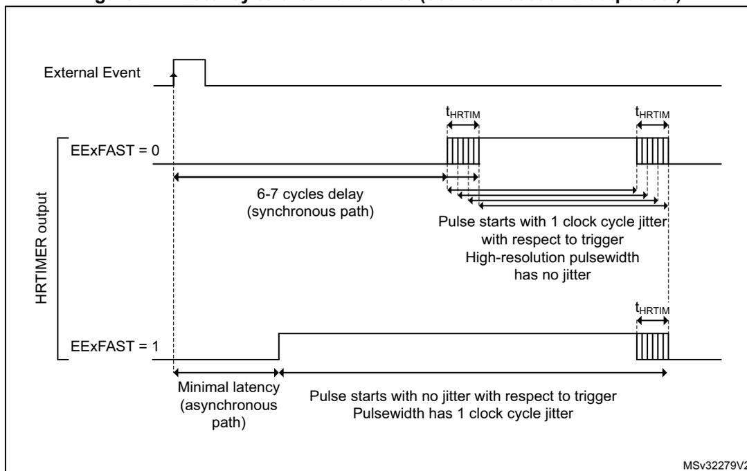
External Event
HRTIMER output
EExFAST = 0
6-7 cycles delay (synchronous path)
\( t_{HRTIM} \)
Pulse starts with 1 clock cycle jitter with respect to trigger
High-resolution pulsewidth has no jitter
EExFAST = 1
Minimal latency (asynchronous path)
Pulse starts with no jitter with respect to trigger
Pulsewidth has 1 clock cycle jitter
MSv32279V2
Figure 245. Latency to external events (output reset on external event)
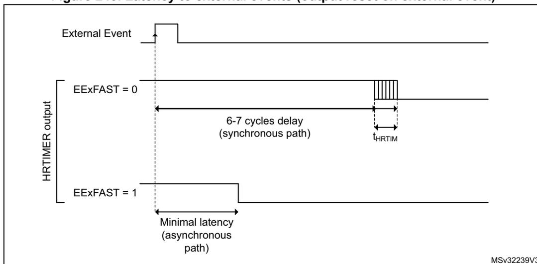
External Event
HRTIMER output
EExFAST = 0
6-7 cycles delay (synchronous path)
\( t_{HRTIM} \)
EExFAST = 1
Minimal latency (asynchronous path)
MSv32239V3
28.3.9 External event filtering in timing units
Once conditioned, the 10 external events are available for all timing units.
They can be used directly and are active as soon as the timing unit counter is enabled (TxCEN bit set).
They can also be filtered to have an action limited in time, usually related to the counting period. Two operations can be performed:
- • blanking, to mask external events during a defined time period,
- • windowing, to enable external events only during a defined time period.
These modes are enabled using HRTIM_EExFLTR[3:0] bits in the HRTIM_EEFxR1 and HRTIM_EEFxR2 registers. Each of the 6 timer A..F timing units has its own programmable filter settings for the 10 external events.
Blanking mode
In event blanking mode (see Figure 246 ), the external event is ignored if it happens during a given blanking period. This is convenient, for instance, to avoid a current limit to trip on switching noise at the beginning of a PWM period. This mode is active for EExFLTR[3:0] bitfield values ranging from 0001 to 1100.
Figure 246. Event blanking mode
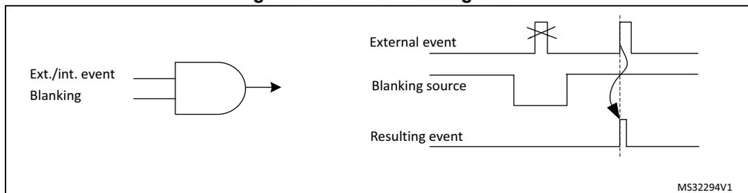
In event postpone mode, the external event is not taken into account immediately but is memorized (latched) and generated as soon as the blanking period is completed, as shown on Figure 247 . This mode is enabled by setting EExLTCH bit in HRTIM_EEFxR1 and HRTIM_EEFxR2 registers.
Figure 247. Event postpone mode
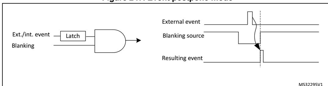
The blanking signal comes from several sources:
- • the timer itself: the blanking lasts from the counter reset to the compare match (EExFLTR[3:0] = 0001 to 0100 for compare 1 to compare 4). In up/down mode (UDM bit set to 1), the counter reset event is defined as per the ROM[1:0] bit setting.
- • from other timing units (EExFLTR[3:0] = 0101 to 1100): the blanking lasts from the selected timing unit counter reset to one of its compare match, or can be fully programmed as a waveform on Tx2 output. In this case, events are masked as long as the Tx2 signal is inactive (it is not necessary to have the output enabled, the signal is taken prior to the output stage).
The EExFLTR[3:0] configurations from 0101 to 1100 are referred to as TIMFLTR1 to TIMFLTR8 in the bit description, and differ from one timing unit to the other. Table 242 gives the 8 available options per timer: CMPx refers to blanking from counter reset to compare match, Tx2 refers to the timing unit TIMx output 2 waveform defined with HRTIM_SETx2 and HRTIM_RSTx2 registers. For instance, timer B (TIMFLTR6) is timer C output 2 waveform.
Table 242. Filtering signals mapping per timer
| Source | Timer A | Timer B | Timer C | Timer D | Timer E | Timer F | |||||||||||||||||||
|---|---|---|---|---|---|---|---|---|---|---|---|---|---|---|---|---|---|---|---|---|---|---|---|---|---|
| CMP1 | CMP2 | CMP4 | TA2 | CMP1 | CMP2 | CMP4 | TB2 | CMP1 | CMP2 | CMP4 | TC2 | CMP1 | CMP2 | CMP4 | TD2 | CMP1 | CMP2 | CMP4 | TE2 | CMP1 | CMP2 | CMP4 | TF2 | ||
| Destination | Timer A | - | - | - | - | 1 | - | 2 | 3 | 4 | - | 5 | - | 7 | - | - | - | 8 | - | - | - | 6 | - | - | - |
| Timer B | 1 | - | 2 | 3 | - | - | - | - | 4 | 5 | - | - | - | 7 | - | - | 8 | - | - | - | - | 6 | - | - | |
| Timer C | - | 1 | - | - | 2 | - | 3 | - | - | - | - | - | 5 | - | 6 | 7 | - | - | 8 | - | 4 | - | - | - | |
| Timer D | 1 | - | - | - | - | 2 | - | - | 3 | 4 | - | 5 | - | - | - | - | 6 | - | 7 | 8 | - | - | 8 | - | |
| Timer E | - | 1 | - | - | 2 | - | - | - | 3 | - | - | - | 6 | - | 7 | 8 | - | - | - | - | - | - | 4 | 5 | |
| Timer F | - | - | 1 | - | - | 2 | - | - | - | - | 3 | - | - | 4 | 5 | - | 6 | - | 7 | 8 | - | - | - | - | |
Figure 248 and Figure 249 give an example of external event blanking for all edge and level sensitivities, in regular and postponed modes.
Figure 248. External trigger blanking with edge-sensitive trigger
![Timing diagram showing external trigger blanking with edge-sensitive trigger. It displays the Counter, Compare 1, Blanking window, External event, EExLTCH = 0, EExLTCH = 1, and EExSNS[1:0] settings. The diagram illustrates how the external event is filtered by the blanking window to generate an internal event.](/RM0440-STM32G4/4f6eee2867eef27c784a16b46d1baadd_img.jpg)
The timing diagram illustrates the external trigger blanking process. The 'Counter' shows a sawtooth waveform. 'Compare 1' shows a horizontal line representing a comparison value. The 'Blanking window' is a rectangular pulse that is high during the counter's active period. The 'External event' shows a series of pulses. Below the external event, two rows show the effect of different sensitivity settings (EExSNS[1:0]). For EExLTCH = 0, the output is high for rising edges (01), low for falling edges (10), and high for both (11). For EExLTCH = 1, the output is high for falling edges (10), low for rising edges (01), and high for both (11). Vertical dashed lines indicate the timing of the external event pulses relative to the blanking window. An arrow at the bottom indicates the 'Internal event generated after blanking' which occurs when an external event falls within the blanking window and matches the configured sensitivity.
Figure 249. External trigger blanking, level sensitive triggering
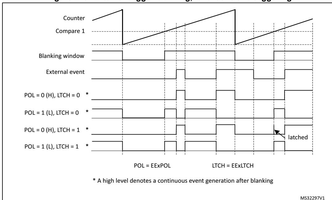
Counter
Compare 1
Blanking window
External event
POL = 0 (H), LTCH = 0 *
POL = 1 (L), LTCH = 0 *
POL = 0 (H), LTCH = 1 *
POL = 1 (L), LTCH = 1 *
latched
POL = EExPOL
LTCH = EExLTCH
* A high level denotes a continuous event generation after blanking
MS32297V1
Windowing mode
In event windowing mode, the event is taken into account only if it occurs within a given time window, otherwise it is ignored. This mode is active for EExFLTR[3:0] ranging from 1101 to 1111.
Figure 250. Event windowing mode
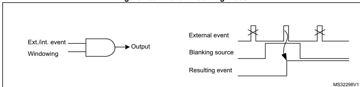
Ext./int. event
Windowing
Output
External event
Blanking source
Resulting event
MS32298V1
EExLTCH bit in EEFxR1 and EEFxR2 registers allows to latch the signal, if set to 1: in this case, an event is accepted if it occurs during the window but is delayed at the end of it.
- • If EExLTCH bit is reset and the signal occurs during the window, it is passed through directly.
- • If EExLTCH bit is reset and no signal occurs, a timeout event is generated at the end of the window.
A use case of the windowing mode is to filter synchronization signals. The timeout generation allows to force a default synchronization event, when the expected synchronization event is lacking (for instance during a converter start-up).
There are 3 sources for each external event windowing, coded as follows:
- • 1101 and 1110: the windowing lasts from the counter reset to the compare match (respectively compare 2 and compare 3). In up/down mode (UDM bit set to 1), the counter reset event is defined as per the ROM[1:0] bit setting.
- • 1111: the windowing is related to another timing unit and lasts from its counter reset to its compare 2 match. The source is described as TIMWIN in the bit description and is given in Table 243 . As an example, the external events in timer B can be filtered by a window starting from timer A counter reset to timer A compare 2.
Table 243. Windowing signals mapping per timer (EEFLTR[3:0] = 1111)
| Destination | Timer A | Timer B | Timer C | Timer D | Timer E | Timer F |
|---|---|---|---|---|---|---|
| TIMWIN (source) | Timer B CMP2 | Timer A CMP2 | Timer D CMP2 | Timer C CMP2 | Timer F CMP2 | Timer E CMP2 |
Note: The timeout event generation is not supported if the external event is programmed in fast mode.
Figure 251 and Figure 252 present how the events are generated for the various edge and level sensitivities, as well as depending on EExLTCH bit setting. Timeout events are specifically mentioned for clarity reasons.
Figure 251. External trigger windowing with edge-sensitive trigger
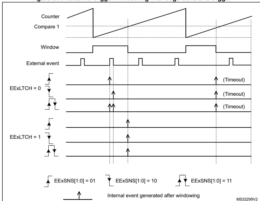
The figure is a timing diagram illustrating external trigger windowing with an edge-sensitive trigger. It shows the relationship between the Counter, Compare 1, Window, External event, and EExLTCH settings. The Counter is a sawtooth wave. Compare 1 is a horizontal line. The Window is a pulse that is high when the Counter is between Compare 1 and the next compare match. The External event is a series of pulses. The EExLTCH settings are shown for two cases: EExLTCH = 0 and EExLTCH = 1. For EExLTCH = 0, the external event is filtered by the window for rising, falling, and both edges. For EExLTCH = 1, the external event is filtered by the window for rising and falling edges. The legend indicates the edge-sensitive trigger settings: EExSNS[1:0] = 01 (rising edge), EExSNS[1:0] = 10 (falling edge), and EExSNS[1:0] = 11 (both edges). Timeout events are shown for external events that occur outside the window.
Figure 252. External trigger windowing, level sensitive triggering
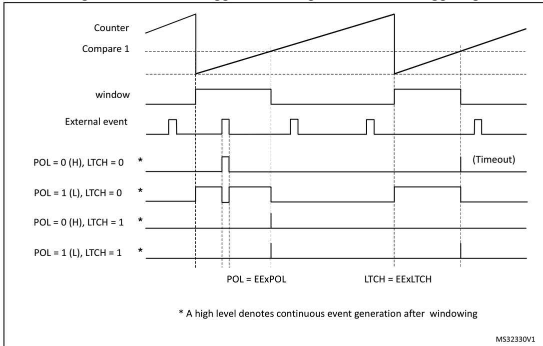
External event counter
Each timing unit also features an external event counter following the filtering unit, typically for valley skipping implementation.
The circuitry allows to filter any of the 10 external events filtered, as shown on Figure 253.
Figure 253. External event counter – channel A
![Block diagram of the external event counter for channel A. It shows 10 external events (1-10) being multiplexed by EEVASEL[3:0] to produce 'External event A'. This signal enters a 'Counter external event A' block. The counter is controlled by EEVACNT[5:0], EEVARSTM, and EEVACRES. A 'Reset/roll-over event' is also input to the counter. The counter output is multiplexed back to the 10 external events by another EEVASEL[3:0] block. Reference MSV47422V1.](/RM0440-STM32G4/3b44dfcba93e2f1dba1c3a8337863e23_img.jpg)
The counter is enabled using the EEVACE bit in the HRTIM_EEFxR3 register. This mode is only valid for edge-sensitive external events (EEASNS[1:0] bit = 01, 10 or 11).
The external event is propagated to the timer only if the number of active edges is greater or equal to the value programmed in (EEVACNT[5:0]+1).
Two operating modes are available:
- • when the EEVARSTM bit is reset, the external event counter is reset on each reset/rollover event: the external event is active only if it appears several times within a given PWM period
- • when the EEVARSTM/ bit is set, the external event counter is reset only if the event did not appear during the last PWM period. This is a cumulative mode, where the event must occur at least once during multiple PWM period, as shown on Figure 254 below.
The external event counter must be enabled after having programmed the counter value (the EEVACE bit must be set after having written the EEVACNT[5:0] bits).
Once the counter is enabled, the EEVACNT[5:0] bits can then be changed on-the-fly at any time. The new value is taken into account on the following reset/rollover event as per the EEVARSTM bit programming, or after a software reset (EEVACRES bit set).
The EEVASEL[3:0] bits must not be modified once the EEVACE bit is set.
Figure 254. External event counter cumulative mode (EEVxRSTM = 1, EEVxCNT = 2)
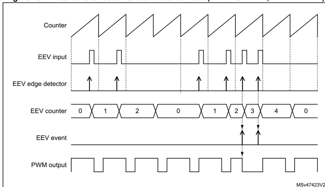
28.3.10 Delayed protection
The HRTIM features specific protection schemes, typically for resonant converters when it is necessary to shut down the PWM outputs in a delayed manner, either once the active pulse is completed or once a push-pull period is completed. These features are enabled with DLYPRTEN bit in the HRTIM_OUTxR register, and are using specific external event channels.
Delayed idle
In this mode, the active pulse is completed before the protection is activated. The selected external event causes the output to enter in idle mode at the end of the active pulse (defined by an output reset event in HRTIM_RSTx1R or HRTIM_RSTx2R).
Once the protection is triggered, the idle mode is permanently maintained but the counter continues to run, until the output is re-enabled. Tx1OEN and Tx2OEN bits are not affected
by the delayed idle entry. To exit from delayed idle and resume operation, it is necessary to overwrite Tx1OEN and Tx2OEN bits to 1. The output state changes on the first transition to an active state following the output enable command.
Note: The delayed idle mode cannot be exited immediately after having been entered, before the active pulse is completed: it is mandatory to make sure that the outputs are in idle state before resuming the run mode. This can be done by waiting up to the next period, for instance, or by polling the O1CPY and/or O2CPY status bits in the TIMxISR register.
The delayed idle mode can be applied to a single output (DLYPRT[2:0] = x00 or x01) or to both outputs (DLYPRT[2:0] = x10).
An interrupt or a DMA request can be generated in response to a Delayed Idle mode entry. The DLYPRT flag in HRTIM_TIMxISR is set as soon as the external event arrives, independently from the end of the active pulse on output.
When the Delayed Idle mode is triggered, the output states can be determined using O1STAT and O2STAT in HRTIM_TIMxISR. Both status bits are updated even if the delayed idle is applied to a single output. When the push-pull mode is enabled, the IPPSTAT flag in HRTIM_TIMxISR indicates during which period the delayed protection request occurred.
This mode is available whatever the timer operating mode (regular, push-pull, deadtime). It is available with 2 external events only:
- • hrtim_eev6 and hrtim_eev7 for timer A, B and C
- • hrtim_eev8 and hrtim_eev9 for timer D, E and F
The delayed protection mode can be triggered only when the counter is enabled (TxCEN bit set). It remains active even if the TxEN bit is reset, until the TxyOEN bits are set.
Figure 255. Delayed Idle mode entry
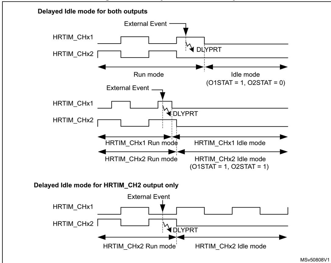
Delayed Idle mode for both outputs
MSv50808V1
The delayed idle mode has a higher priority than the burst mode: any burst mode exit request is discarded once the delayed idle protection has been triggered. On the contrary, If the delayed protection is exited while the burst mode is active, the burst mode is resumed normally and the output is maintained in the idle state until the burst mode exits. Figure 256 gives an overview of these different scenarios.
Figure 256. Burst mode and delayed protection priorities (DIDL = 0)
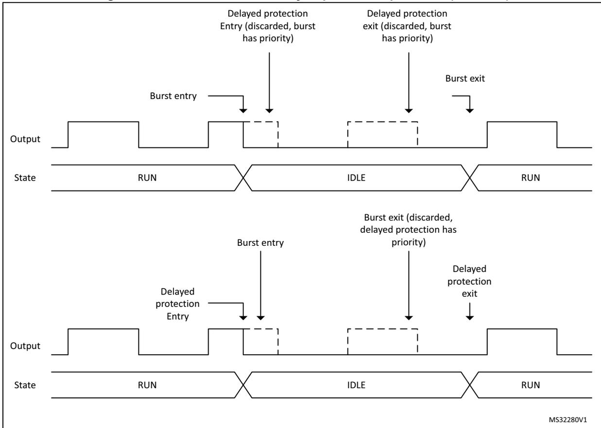
The figure consists of two timing diagrams illustrating the interaction between burst mode and delayed protection in an HRTIM output. Both diagrams show the 'Output' signal and the 'State' over time.
Top Diagram:
- The output starts high (RUN state).
- A 'Burst entry' occurs, causing the output to go low.
- Shortly after, a 'Delayed protection Entry' is requested but discarded because the burst mode has priority.
- Later, a 'Delayed protection exit' is requested but discarded for the same reason.
- Finally, a 'Burst exit' occurs, returning the output to high (RUN state).
Bottom Diagram:
- The output starts high (RUN state).
- A 'Delayed protection Entry' is requested and accepted, causing the output to go low.
- Then, a 'Burst entry' occurs, but the output remains low because the delayed protection is active.
- Later, a 'Burst exit' is requested but discarded because the delayed protection has priority.
- Finally, a 'Delayed protection exit' occurs, returning the output to high (RUN state).
The state transitions are labeled as RUN, IDLE, and RUN. The IDLE state corresponds to the low output level.
MS32280V1
The same priorities are applied when the delayed burst mode entry is enabled (DIDL bit set), as shown on Figure 257 .
Figure 257. Burst mode and delayed protection priorities (DIDL = 1)
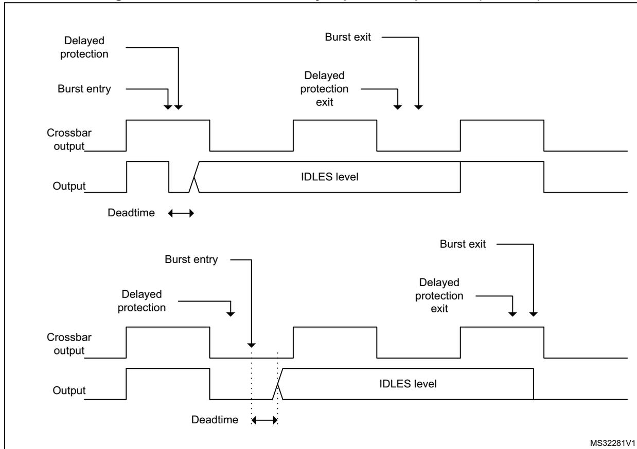
The figure consists of two timing diagrams illustrating the behavior of HRTIM outputs during burst mode with delayed protection priorities (DIDL = 1).
Top Diagram: Shows the sequence of events when a burst entry occurs while the output is active.
- Crossbar output: A square wave that is high during the active period.
- Output: A square wave that is high during the active period and goes to an IDLES level (low) when protection is active.
- Burst entry: An event that triggers the start of burst mode.
- Delayed protection: A protection signal that goes low after a short delay from the burst entry.
- Deadtime: The time interval between the falling edge of the crossbar output and the falling edge of the output.
- Burst exit: An event that triggers the end of burst mode.
- Delayed protection exit: A protection signal that goes high after a short delay from the burst exit.
Bottom Diagram: Shows the sequence of events when a burst entry occurs while the output is already in the IDLES level.
- Crossbar output: A square wave that is high during the active period.
- Output: A square wave that is initially low (IDLES level), goes high when the burst entry occurs, and returns to the IDLES level when protection is active.
- Burst entry: An event that triggers the start of burst mode.
- Delayed protection: A protection signal that goes low after a short delay from the burst entry.
- Deadtime: The time interval between the falling edge of the crossbar output and the falling edge of the output.
- Burst exit: An event that triggers the end of burst mode.
- Delayed protection exit: A protection signal that goes high after a short delay from the burst exit.
MS32281V1
Balanced idle
Only available in push-pull mode, the balanced idle allows to have a balanced pulsemode on the two outputs when one of the active pulse is shortened due to a protection. The pulsemode, terminated earlier than programmed, is copied on the alternate output, then the two outputs are put in idle state, until the normal operation is resumed by software. This mode is enabled by writing x11 in DLYPRT[2:0] bitfield in HRTIM_OUTxR.
This mode is available with only 2 external events:
- • hrtim_eev6 and hrtim_eev7 for timer A, B and C
- • hrtim_eev8 and hrtim_eev9 for timer D, E and F
Figure 258. Balanced Idle protection example
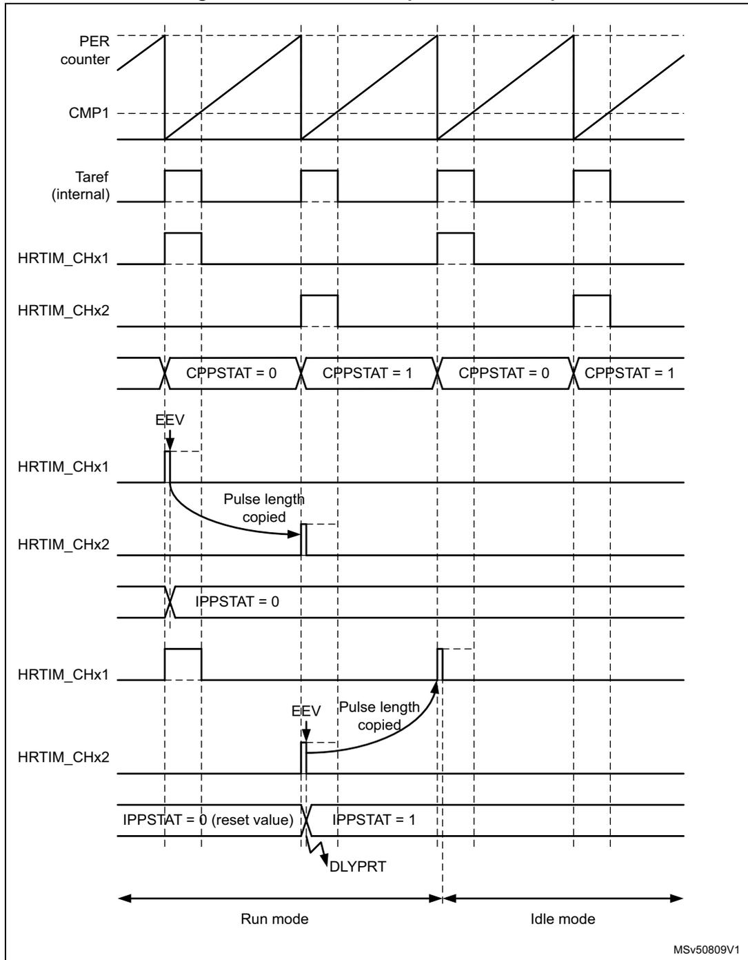
The diagram illustrates the timing for a balanced idle protection example. It shows the following signals and states:
- PER counter: A sawtooth waveform representing the timer counter.
- CMP1: A constant reference level for comparison.
- Taref (internal): A periodic square wave reference signal.
- HRTIM_CHx1: Output channel 1. In Run mode, it is a short pulse. In Idle mode, it is a long pulse.
- HRTIM_CHx2: Output channel 2. In Run mode, it is a short pulse. In Idle mode, it is a long pulse.
- CPPSTAT: Capture/Pulse Width Protection Status register. It alternates between CPPSTAT = 0 and CPPSTAT = 1 in Run mode.
- EEV: External Event. A falling edge triggers a capture of the counter value into the compare 4 active register. Arrows labeled "Pulse length copied" show the transfer of pulse width information from CHx1 to CHx2 and from CHx2 to CHx1.
- IPPSTAT: Input Pulse Width Protection Status register. It starts at IPPSTAT = 0 (reset value) in Run mode and transitions to IPPSTAT = 1 when entering Idle mode.
- DLYPRT: Delay Protection flag, indicated by a pulse when entering Idle mode.
- Run mode: The initial phase where the timer is active and outputs are short pulses.
- Idle mode: The phase entered after the idle protection logic is triggered, where outputs maintain their last state for one additional period before taking the idle level.
MSV50809V1
When the balanced Idle mode is enabled, the selected external event triggers a capture of the counter value into the compare 4 active register (this value is not user-accessible). The push-pull is maintained for one additional period so that the shorten pulse can be repeated: a new output reset event is generated while the regular output set event is maintained.
The Idle mode is then entered and the output takes the level defined by IDLESx bits in the HRTIM_OUTxR register. The balanced idle mode entry is indicated by the DLYPRT flag.
while the IPPSTAT flag indicates during which period the external event occurred, to determine the sequence of shorten pulses (A1 then A2 or vice versa).
The timer operation is not interrupted (the counter continues to run).
To enable the balanced idle mode, it is necessary to have the following initialization:
- – timer operating in continuous mode (CONT = 1)
- – Push-pull mode enabled
- – HRTIM_CMP4xR must be set to 0 and the content transferred into the active register (for instance by forcing a software update)
- – DELCMP4[1:0] bit field must be set to 00 (auto-delayed mode disabled)
- – DLYPRT[2:0] = x11 (delayed protection enable)
Note: The HRTIM_CMP4xR register must not be written during a balanced idle operation. The CMP4 event is reserved and cannot be used for another purpose.
In balanced idle mode, it is recommended to avoid multiple external events or software-based reset events causing an output reset. If such an event arrives before a balanced idle request within the same period, it causes the output pulses to be unbalanced (1st pulse length defined by the external event or software reset, while the 2nd pulse is defined by the balanced idle mode entry).
The minimum pulsewidth that can be handled in balanced idle mode is 4 \( f_{\text{HRTIM}} \) clock periods (0x80 if CKPSC[2:0] = 0, 0x40 if CKPSC[2:0] = 1, 0x20 if CKPSC[2:0] = 2,...).
If the capture occurs before the counter has reached this minimum value, the current pulse is extended up to 4 \( f_{\text{HRTIM}} \) clock periods before being copied into the secondary output. In any case, the pulsewidths are always balanced.
Tx1OEN and Tx2OEN bits are not affected by the balanced idle entry. To exit from balanced idle and resume the operation, it is necessary to overwrite Tx1OEN and Tx2OEN bits to 1 simultaneously. The output state changes on the first active transition following the output enable.
It is possible to resume operation similarly to the delayed idle entry. For instance, if the external event arrives while output 1 is active (delayed idle effective after output 2 pulse), the re-start sequence can be initiated for output 1 first. To do so, it is necessary to poll CPPSTAT bit in the HRTIM_TIMxISR register. Using the above example (IPPSTAT flag equal to 0), the operation is resumed when CPPSTAT bit is 0.
In order to have a specific re-start sequence, it is possible to poll the CPPSTAT to know which output is active first. This allows, for instance, to re-start with the same sequence as the idle entry sequence: if the external event arrives during output 1 active, the re-start sequence is initiated when the output 1 is active (CPPSTAT = 0).
Note: The balanced idle mode must not be disabled while a pulse balancing sequence is ongoing. It is necessary to wait until the CMP4 flag is set, thus indicating that the sequence is completed, to reset the DLYPRTEN bit.
The balanced idle protection mode can be triggered only when the counter is enabled (TxCEN bit set). It remains active even if the TxCEN bit is reset, until TxyOEN bits are set.
Balanced idle can be used together with the burst mode under the following conditions:
- • TxBM bit must be reset (counter clock maintained during the burst, see Section 28.3.15 ),
- • No balanced idle protection must be triggered while the outputs are in a burst idle state.
The balanced idle mode has a higher priority than the burst mode: any burst mode exit request is discarded once the balanced idle protection has been triggered. On the contrary, if the delayed protection is exited while the burst mode is active, the burst mode is resumed normally.
- Note: Although the output state is frozen in idle mode, a number of events are still generated on the auxiliary outputs (see Section 28.3.18 ) during the idle period following the delayed protection:
- - Output set/reset interrupt or DMA requests
- - External event filtering based on output signal
- - Capture events triggered by set/reset
Balanced idle automatic resuming
The balanced Idle mode can be configured to have an automatic resuming of operation after a trigger.
Once the shorten pulse has been copied to the alternate output, the pulse width is reset to its original value and the timer resumes operation: the two outputs keep on being in RUN mode.
This is enabled by setting the BIAR bit in the HRTIM_OUTxR register.
This mode must be used only when the period in HRTIM_PERxR is greater than 6 periods of the \( f_{HRTIM} \) clock (0xC0 if CKPSC[2:0] = 0, 0x60 if CKPSC[2:0] = 1, 0x30 if CKPSC[2:0] = 2, ...).
Note: This bit is only significant if DLYPRT[2:0] = 011 or 111, it is ignored otherwise.
Note: In balanced idle automatic resuming mode, it is mandatory to set the IDLES state to inactive.
28.3.11 Register preload and update management
Most of HRTIM registers are buffered and can be preloaded if needed. Typically, this allows to prevent the waveforms from being altered by a register update not synchronized with the active events (set/reset).
When the preload mode is enabled, accessed registers are shadow registers. Their content is transferred into the active register after an update request, either software or synchronized with an event.
By default, PREEN bits in HRTIM_MCR and HRTIM_TIMxCR registers are reset and the registers are not preloaded: any write directly updates the active registers. If PREEN bit is reset while the timer is running and preload was enabled, the content of the preload registers is directly transferred into the active registers.
Each timing unit and the master timer have their own PREEN bit. If PRREN is set, the preload registers are enabled and transferred to the active register only upon an update event.
There are two options to initialize the timer when the preload feature is needed:
- • Enable PREEN bit at the very end of the timer initialization to have the preload registers transferred into the active registers before the timer is enabled (by setting MCEN and TxCEN bits).
- • enable PREEN bit at any time during the initialization and force a software update immediately before starting.
Table 244 lists the registers which can be preloaded, together with a summary of available update events.
Table 244. HRTIM preloadable control registers and associated update sources
| Timer | Preloadable registers | Preload enable | Update sources |
|---|---|---|---|
| Master timer | HRTIM_DIER HRTIM_MPER HRTIM_MREP HRTIM_MCMP1R HRTIM_MCMP2R HRTIM_MCMP3R HRTIM_MCMP4R | PREEN bit in HRTIM_MCR | Software Repetition event Burst DMA event Repetition event following a burst DMA event |
| Timer x x = A..F | HRTIM_TIMxDIER HRTIM_TIMxPER HRTIM_TIMxREP HRTIM_TIMxCMP1R HRTIM_TIMxCMP1CR HRTIM_TIMxCMP2R HRTIM_TIMxCMP3R HRTIM_TIMxCMP4R HRTIM_DTxR HRTIM_SETx1R HRTIM_RSTx1R HRTIM_SETx2R HRTIM_RSTx2R HRTIM_RSTxR | PREEN bit in HRTIM_TIMxCR | Software TIMx repetition event TIMx reset event Burst DMA event Update event from other timers (TIMy, master) Update event following a burst DMA event Update enable inputs hrtim_upd_en[3:1] Update event following an update enable input following an update event on hrtim_upd_en[3:1] inputs |
| HRTIM Common | HRTIM_ADC1R HRTIM_ADC2R HRTIM_ADC3R HRTIM_ADC4R | TIMx or master timer Update, depending on ADxUSRC[2:0] bits in HRTIM_CR1, if PREEN = 1 in the selected timer |
The master timer has 4 update options:
- 1. Software: writing 1 into MSWU bit in HRTIM_CR2 forces an immediate update of the registers. In this case, any pending hardware update request is cancelled.
- 2. Update done when the master counter rolls over and the master repetition counter is equal to 0. This is enabled when MREPU bit is set in HRTIM_MCR.
- 3. Update done once burst DMA is completed (see Section 28.3.23 for details). This is enabled when BRSTDMA[1:0] = 01 in HRTIM_MCR. It is possible to have both MREPU=1 and BRSTDMA=01.
Note: The update can take place immediately after the end of the burst sequence if SWU bit is set (i.e. forced update mode). If SWU bit is reset, the update is done on the next update event following the end of the burst sequence.
- 4. Update done when the master counter rolls over following a burst DMA completion. This is enabled when BRSTDMA[1:0] = 10 in HRTIM_MCR.
An interrupt or a DMA request can be generated by the master update event.
Each timer (TIMA..F) can also have the update done as follows:
- • By software: writing 1 into TxSWU bit in HRTIM_CR2 forces an immediate update of the registers. In this case, any pending hardware update request is canceled.
- • Update done when the counter rolls over and the repetition counter is equal to 0. This is enabled when TxREPU bit is set in HRTIM_TIMxCR.
- • Update done when the counter is reset or rolls over in continuous mode. This is enabled when TxRSTU bit is set in HRTIM_TIMxCR. This is used for a timer operating in single-shot mode, for instance.
- • Update done once a burst DMA is completed. This is enabled when UPDGAT[3:0] = 0001 in HRTIM_TIMxCR.
- • Update done on the update event following a burst DMA completion (the event can be enabled with TxRSTU, TxREPU, MSTU or TxU). This is enabled when UPDGAT[3:0] = 0010 in HRTIM_TIMxCR.
- • Update done when receiving a request on hrtim_upd_en[3:1]. This is enabled when UPDGAT[3:0] = 0011, 0100, 0101 in HRTIM_TIMxCR.
- • Update done on the update event following a request on hrtim_upd_en[3:1] (the event can be enabled with TxRSTU, TxREPU, MSTU or TxU). This is enabled when UPDGAT[3:0] = 0110, 0111, 1000 in HRTIM_TIMxCR
- • Update done synchronously with any other timer or master update (for instance TIMA can be updated simultaneously with TIMB). This is used for converters requiring several timers, and is enabled by setting bits MSTU and TxU in HRTIM_TIMxCR register.
The update enable inputs hrtim_upd_en[3:1] allow to have an update event synchronized with on-chip events coming from the general-purpose timers. These inputs are rising-edge sensitive.
Table 224 lists the connections between update enable inputs and the on-chip sources.
This allows to synchronize low frequency update requests with high-frequency signals (for instance an update on the counter roll-over of a 100 kHz PWM that has to be done at a 100 Hz rate).
Note: The update events are synchronized to the prescaler clock when CKPSC[2:0] > 5.
The update coming from adjacent timers (when MSTU, TAU, TBU, TCU, TDU, TEU, TFU bit is set) or from a software update (TxSWU bit) can either be taken into account immediately or re-synchronized with the timers reset/roll-over event. This is done with the RSYNCU bit in the HRTIM_TIMxCR register, as show on Figure 259 below):
- – RSYNCU = 0: The update coming from adjacent timers is taken into account immediately
- – RSYNCU = 1: The update coming from adjacent timers is taken into account on the following reset/roll-over event.
The RSYNCU bit is significant only when UPDGAT[3:0] = 0000, it is ignored otherwise.
An interrupt or a DMA request can be generated by the Timx update event.
Figure 259. Resynchronized timer update (TAU=1 in HRTIM_TIMBCR)
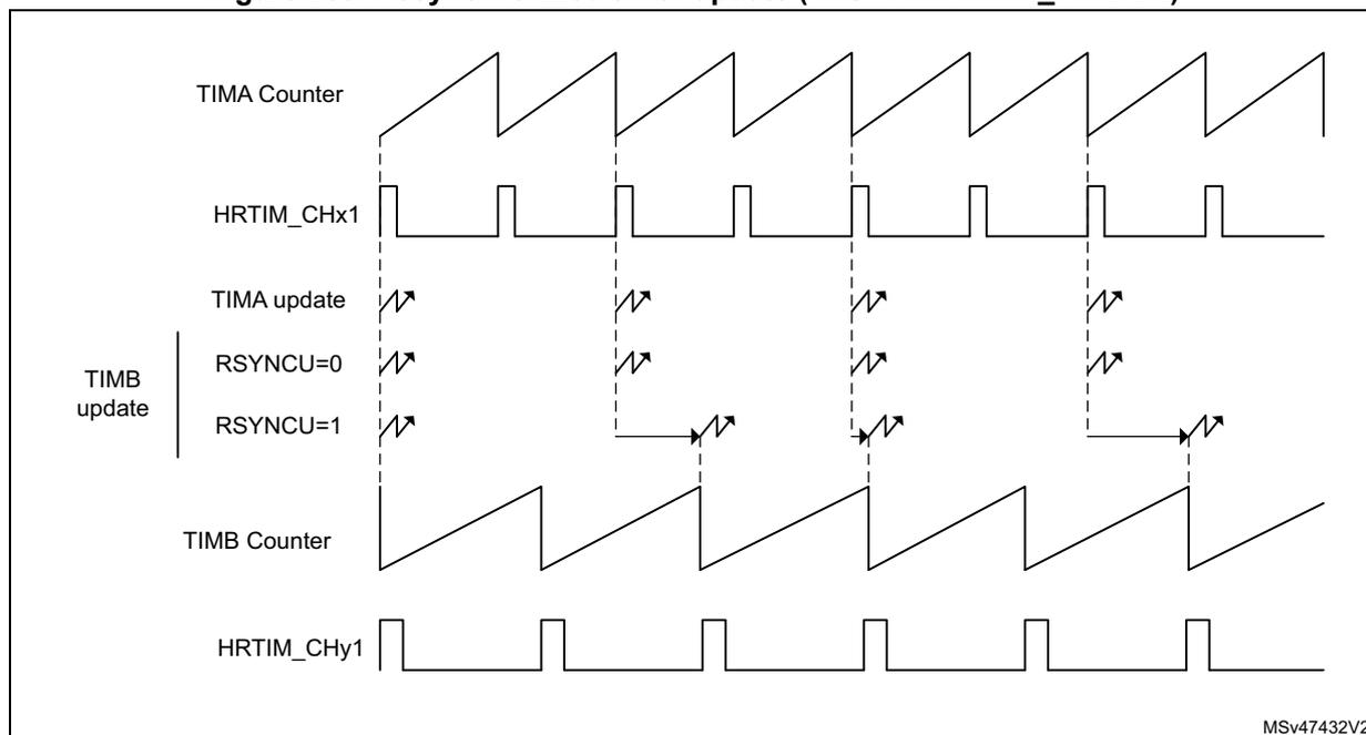
MUDIS and TxUDIS bits in the HRTIM_CR1 register allow to temporarily disable the transfer from preload to active registers, whatever the selected update event. This allows to modify several registers in multiple timers. The regular update event takes place once these bits are reset.
MUDIS and TxUDIS bits are all grouped in the same register. This allows the update of multiple timers (not necessarily synchronized) to be disabled and resumed simultaneously.
The following example is a practical use case. A first power converter is controlled with the master, TIMB and TIMC. TIMB and TIMC must be updated simultaneously with the master timer repetition event. A second converter works in parallel with TIMA, TIMD and TIME, and TIMD, TIME must be updated with TIMA repetition event.
First converter
In HRTIM_MCR, MREPU bit is set: the update occurs at the end of the master timer counter repetition period. In HRTIM_TIMBCR and HRTIM_TIMCCR, MSTU bits are set to have TIMB and TIMC timers updated simultaneously with the master timer.
When the power converter set-point has to be adjusted by software, MUDIS, TBUDIS and TCUDIS bits of the HRTIM_CR register must be set prior to write accessing registers to update the values (for instance the compare values). From this time on, any hardware update request is ignored and the preload registers can be accessed without any risk to have them transferred into the active registers. Once the software processing is over, MUDIS, TBUDIS and TCUDIS bits must be reset. The transfer from preload to active registers is done as soon as the master repetition event occurs.
Second converter
In HRTIM_TIMACR, TAREPU bit is set: the update occurs at the end of the timer A counter repetition period. In HRTIM_TIMDCR and HRTIM_TIMECR, TAU bits are set to have TIMD and TIME timers updated simultaneously with timer A.
When the power converter set-point has to be adjusted by software, TAUDIS, TDUDIS and TEUDIS bits of the HRTIM_CR register must be set prior to write accessing the registers to update the values (for instance the compare values). From this time on, any hardware update request is ignored and the preload registers can be accessed without any risk to have them transferred into the active registers. Once the software processing is over, TAUDIS, TDUDIS and TEUDIS bits can be reset: the transfer from preload to active registers is done as soon as the timer A repetition event occurs.
28.3.12 PWM mode with “greater than” comparison
A specific no-latency update mode is available for PWM signals generated with the CMP1 and CMP3 registers. It allows to have a new duty cycle value applied as soon as possible within the PWM cycle, without having to wait the completion of the current PWM period. This reduces the overall delay time in software control loops. As shown on Figure 260 below, this eventually allows to have:
- – an early turn-off of the output if the new compare value is below the current counter value and the current compare value is above the counter, at the time the new value is written.
- – an early turn-on of the output, re-enabling the output if the new compare value is above the counter value and the current compare value is above the counter, at the time the new value is written.
The output signal is left unchanged when the new compare value and current compare value are both below the counter.
This feature is only available for CMP1 or CMP3 RESET events, and is enabled using the GTCMP1 and GTCMP3 enable bits in the HRTIM_TIMxCR2 register.
The preload mechanism is inactive for a compare register when the corresponding GTCMPx bit is set, whatever the PREEN bit value. This mode is intended to have the new compare value taken into account as soon as possible after a new value write, without waiting for the preload to active register transfer.
These bits are defining the compare 1 and compare 3 operating modes as following
- – GTCMPx = 0: the compare x event is generated when the counter is equal to the compare value (compare match mode). If the compare value is changed on-the-fly, the compare event may not be generated.
- – GTCMPx = 1: the compare x event is generated when the counter is greater than the compare value. If the compare value is changed on-the-fly, the new compare value is compared with the current counter value and an output SET or RESET can be generated.
The “greater than” compare mode causes the crossbar to act differently depending on comparison result. Let’s consider the CMP1 event is doing an output RESET. When the new compare value is written, two cases are considered
- – If the new compare value is below the counter value, the RESET event is issued and can eventually cause an early turn-OFF
- – If the new compare value is above the counter value, a SET event is generated so as to re-arm the output value before it is actually RESET when the counter exceeds the counter value (early turn-ON).
The “greater than” compare mode is supported for both SET and RESET actions.
The “greater than” compare mode must only be used for the following configuration:
- 1. In the fixed frequency configuration, the period event must trigger the output set and the “greater than” compare triggers the output reset (or vice versa the period must trigger the reset if the “greater-than” compare triggers the set).
- 2. For variable frequency configuration, the event selected as counter reset source must also be selected as set or reset source for the timer output (opposite direction as the “greater than” compare event).
Note: The “greater-than” modes must not be used when the CMP1 and/or CMP3 modes are controlled by hardware in half and interleaved modes.
Figure 260. Early turn-ON and early turn-OFF behavior in “greater than” PWM mode
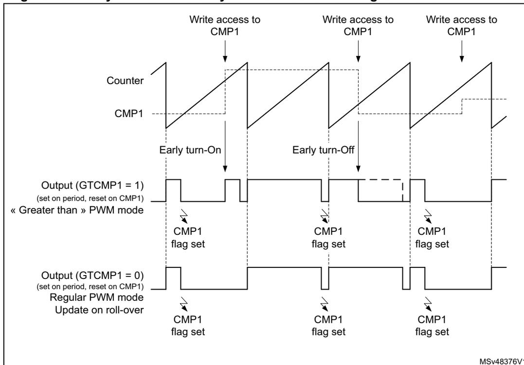
The diagram shows four waveforms over time:
- Counter: A sawtooth waveform that increases linearly and then resets abruptly.
- CMP1: A dashed horizontal line representing the compare value, which is updated at three points labeled “Write access to CMP1”.
- Output (GTCMP1 = 1): (set on period, reset on CMP1) « Greater than » PWM mode. It shows an “Early turn-On” and “Early turn-Off” event.
- Output (GTCMP1 = 0): (set on period, reset on CMP1) Regular PWM mode Update on roll-over.
The immediate update mode implies that the content of the preload register is transferred into the active register at the very same time the register is written. When GTCMP1 and/or GTCMP3 bits are set, their respective preload mechanism is disabled (for HRTIM_TIMxCMP1 and/or HRTIM_TIMxCMP3 registers), whatever the PREEN bit value.
Note: The compare interrupt flags (CMP1 and CMP3 in HRTIM_TIMxISR) are not generated in case of late turn-ON and early turn-OFF, as shown on Figure 260.
Note: The “Greater than” comparison must not be done on both CMP1 and CMP3 for the same output (GTCMP1 and GTCMP3 bits must not be set simultaneously).
28.3.13 Events propagation within or across multiple timers
The HRTIM offers many possibilities for cascading events or sharing them across multiple timing units, including the master timer, to get full benefits from its modular architecture. These are key features for converters requiring multiple synchronized outputs.
This section summarizes the various options and specifies whether and how an event is propagated within the HRTIM.
TIMx update triggered by the master timer update
The sources listed in Table 245 are generating a master timer update. The table indicates if the source event can be used to trigger a simultaneous update in any of TIMx timing units.
Operating condition: MSTU bit is set in HRTIM_TIMxCR register.
Table 245. Master timer update event propagation
| Source | Condition | Propagation | Comment |
|---|---|---|---|
| Burst DMA end | BRSTDMA[1:0] = 01 | No | Must be done in TIMxCR (UPDGAT[3:0] = 0001) |
| Roll-over event following a burst DMA end | BRSTDMA[1:0] = 10 | Yes | - |
| Repetition event caused by a counter roll-over | MREPU = 1 | Yes | - |
| Repetition event caused by a counter reset (from HRTIM_SCIN or software) | No | - | |
| Software update | MSWU = 1 | No | All software update bits (TxSWU) are grouped in the HRTIM_CR2 register and can be used for a simultaneous update |
TIMx update triggered by the TIMy update
The sources listed in Table 246 are generating a TIMy update. The table indicates if the given event can be used to trigger a simultaneous update in another or multiple TIMx timers.
Operating condition: TyU bit set in HRTIM_TIMxCR register (source = TIMy and destination = TIMx).
Table 246. TIMx update event propagation
| Source | Condition | Propagation | Comment |
|---|---|---|---|
| Burst DMA end | UPDGAT[3:0] = 0001 | No | Must be done directly in HRTIM_TIMxCR (UPDGAT[3:0] = 0001) |
| Update caused by the update enable inputs hrtim_upd_en[3:1] | UPDGAT[3:0] = 0011, 0100, 0101 | No | Must be done directly in HRTIM_TIMxCR (UPDGAT[3:0] = 0011, 0100, 0101) |
| Master update | MSTU = 1 in HRTIM_TIMyCR | No | Must be done with MSTU = 1 in HRTIM_TIMxCR |
| Another TIMx update (TIMz>TIMy>TIMx) | TzU=1 in HRTIM_TIMyCR TyU=1 in TIMxCR | No | Must be done with TzU=1 in HRTIM_TIMxCR TzU=1 in HRTIM_TIMyCR |
| Repetition event caused by a counter roll-over | TyREPU = 1 | Yes | - |
| Repetition event caused by a counter reset | TyREPU = 1 | - | Refer to counter reset cases below |
| Counter roll-over | TyRSTU = 1 | Yes | - |
Table 246. TIMx update event propagation (continued)
| Source | Condition | Propagation | Comment |
|---|---|---|---|
| Counter software reset | TyRST=1 in HRTIM_CR2 | No | Can be done simultaneously with update in HRTIM_CR2 register |
| Counter reset caused by a TIMz compare | TIMzCMPn in HRTIM_RSTyR | Yes | - |
| Counter reset caused by external events | EXTEVNTn in HRTIM_RSTyR | Yes | - |
| Counter reset caused by a master compare or a master period | MSTCMPn or MSTPER in HRTIM_RSTyR | Yes | - |
| Counter reset caused by a TIMy compare | CMPn in HRTIM_RSTyR | Yes | - |
| Counter reset caused by an update | UPDT in HRTIM_RSTyR | No | Propagation would result in a lock-up situation (update causing reset causing update) |
| Counter reset caused by HRTIM_SCIN | SYNCRSTy in HRTIM_TIMyCR | No | - |
| Software update | TySWU = 1 | No | All software update bits (TxSWU) are grouped in the HRTIM_CR2 register and can be used for a simultaneous update |
TIMx counter reset causing a TIMx update
Table 247 lists the counter reset sources and indicates whether they can be used to generate an update.
Operating condition: TxRSTU bit in HRTIM_TIMxCR register.
Table 247. Reset events able to generate an update
| Source | Condition | Propagation | Comment |
|---|---|---|---|
| Counter roll-over | - | Yes | - |
| Update event | UPDT in HRTIM_RSTxR | No | Propagation would result in a lock-up situation (update causing a reset causing an update) |
| External event | EXTEVNTn in HRTIM_RSTxR | Yes | - |
| TIMy compare | TIMyCMPn in HRTIM_RSTxR | Yes | - |
| Master compare | MSTCMPn in HRTIM_RSTxR | Yes | - |
| Master period | MSTPER in HRTIM_RSTxR | Yes | - |
| Compare 2 and 4 | CMPn in HRTIM_RSTxR | Yes | - |
| Software | TxRST=1 in HRTIM_CR2 | Yes | - |
| HRTIM_SCIN | SYNCRSTx in HRTIM_TIMxCR | Yes | - |
TIMx update causing a TIMx counter reset
Table 248 lists the update event sources and indicates whether they can be used to generate a counter reset.
Operating condition: UPDT bit set in HRTIM_RSTxR.
Table 248. Update event propagation for a timer reset
| Source | Condition | Propagation | Comment |
|---|---|---|---|
| Burst DMA end | UPDGAT[3:0] = 0001 | Yes | - |
| Update caused by the update enable inputs hrtim_upd_en[3:1] | UPDGAT[3:0] = 0011, 0100, 0101 | Yes | - |
| Master update caused by a roll-over after a burst DMA | MSTU = 1 in HRTIM_TIMxCR BRSTDMA[1:0] = 10 in HRTIM_MCR | Yes | - |
Table 248. Update event propagation for a timer reset (continued)
| Source | Condition | Propagation | Comment |
|---|---|---|---|
| Master update caused by a repetition event following a roll-over | MSTU = 1 in HRTIM_TIMxCR | Yes | - |
| Master update caused by a repetition event following a counter reset (software or due to HRTIM_SCIN) | MREPU = 1 in HRTIM_MCR | No | - |
| Software triggered master timer update | MSTU = 1 in HRTIM_TIMxCR MSWU = 1 in HRTIM_CR2 | No | All software update bits (TxSWU) are grouped in the HRTIM_CR2 register and can be used for a simultaneous update |
| TIMy update caused by a TIMy counter roll-over | TyU = 1 in HRTIM_TIMxCR TyRSTU = 1 in HRTIM_TIMyCR | Yes | - |
| TIMy update caused by a TIMy repetition event | TyU = 1 in HRTIM_TIMxCR TyREPU = 1 in HRTIM_TIMyCR | Yes | - |
| TIMy update caused by an external event or a TIMy compare (through a TIMy reset) | TyU = 1 in HRTIM_TIMxCR TyRSTU = 1 in HRTIM_TIMyCR EXTEVNTn or CMP4/2 in HRTIM_RSTyCR | Yes | - |
| TIMy update caused by sources other than those listed above | TyU = 1 in HRTIM_TIMxCR | No | - |
| Repetition event following a roll-over | TxREPU = 1 in HRTIM_TIMxCR | Yes | - |
| Repetition event following a counter reset | TxREPU = 1 in HRTIM_TIMxCR | No | - |
| Timer reset | TxRSTU = 1 in HRTIM_TIMxCR | No | Propagation would result in a lock-up situation (reset causing an update causing a reset) |
| Software | TxSWU in HRTIM_CR2 | No | - |
28.3.14 Output management
Each timing unit controls a pair of outputs. The outputs have three operating states:
- • RUN: this is the main operating mode, where the output can take the active or inactive level as programmed in the crossbar unit.
- • IDLE: this state is the default operating state after an HRTIM reset, when the outputs are disabled by software or during a burst mode operation (where outputs are temporary disabled during a normal operating mode; refer to Section 28.3.15 for more details). It is either permanently active or inactive.
- • FAULT: this is the safety state, entered in case of a shut-down request on FAULTx inputs. It can be permanently active, inactive or Hi-Z.
The output status is indicated by TxyOEN bit in HRTIM_OENR register and TxyODS bit in HRTIM_ODSR register, as in Table 249 .
Table 249. Output state programming, x= A..F, y = 1 or 2
| TxyOEN (control/status) (set by software, cleared by hardware) | TxyODS (status) | Output operating state |
|---|---|---|
| 1 | x | RUN |
| 0 | 0 | IDLE |
| 0 | 1 | FAULT |
TxyOEN bit is both a control and a status bit: it must be set by software to have the output in RUN mode. It is cleared by hardware when the output goes back in IDLE or FAULT mode. When TxyOEN bit is cleared, TxyODS bit indicates whether the output is in the IDLE or FAULT state. A third bit in the HRTIM_ODISR register allows to disable the output by software.
Figure 261. Output management overview
![Figure 261. Output management overview diagram showing the internal logic of the HRTIM output stage. A Timing Unit block connects to a Chopper block, which is controlled by CPHx. The Chopper output is connected to a 2-to-1 multiplexer. The multiplexer has three inputs: RUN (from the Chopper), IDLE (from an IDLE State block), and FAULT (from a FAULT State block). The multiplexer is controlled by a Status: OEN/ODS register. The output of the multiplexer is connected to an inverter and a POLx input, resulting in the HRTIM_CHxy output. The IDLE State block is controlled by IDLESx and the FAULT State block is controlled by FAULTx[1:0]. The Status: OEN/ODS register is updated by RUN entry (Software (OEN bit set)), IDLE entry (Software (ODIS bit set) or Hardware: Burst / Delayed protection), and FAULT entry (Hardware (FAULTx inputs) or breakpoint).](/RM0440-STM32G4/e125781eb40f490390873b4b2ae2dd61_img.jpg)
Figure 262 summarizes the bit values for the three states and how the transitions are triggered. Faults can be triggered by any external or internal fault source, as listed in
Section 28.3.17 , while the Idle state can be entered when the burst mode or delayed protections are active.
Figure 262. HRTIM output states and transitions
stateDiagram-v2
    [*] --> IDLE
    IDLE --> RUN : OEN bit set
    RUN --> IDLE : ODIS bit set
    IDLE --> FAULT : (Fault or breakpoint* & (FAULTx[1:0] > 0) & OEN = 1)
    FAULT --> IDLE : ODIS bit set
    RUN --> FAULT : Fault (if FAULTx > 0) or breakpoint*
    FAULT --> RUN : OEN bit set

    state "IDLE State" as IDLE {
        OEN = 0
        ODS = 0
    }
    state "RUN State" as RUN {
        O EN = 1
        O DS = X
    }
    state "FAULT State" as FAULT {
        OEN = 0
        ODS = 1
    }

    note right of FAULT : Breakpoint*: this condition is valid only if DBG_HRTIM_STOP = 1
    note right of FAULT : Txy prefix is omitted for clarity: (OEN = TxyOEN, ODIS = TxyODIS, ODS = TxyODS)
    note right of FAULT : MS32333V1
The diagram illustrates the state transitions for HRTIM outputs. It features three states: IDLE, RUN, and FAULT. Transitions are triggered by specific conditions involving OEN, ODIS, and FAULTx bits. The IDLE state is the initial state with OEN=0 and ODS=0. The RUN state is entered from IDLE when OEN is set, with O EN=1 and O DS=X. The FAULT state is entered from IDLE if a fault or breakpoint occurs while OEN=1, or from RUN if a fault or breakpoint occurs. In the FAULT state, OEN=0 and ODS=1. Transitions back to IDLE or RUN from FAULT are triggered by ODIS being set. A note indicates that the Txy prefix is omitted for clarity, and a breakpoint condition is only valid if DBG_HRTIM_STOP = 1.
The FAULT and IDLE levels are defined as active or inactive. Active (or inactive) refers to the level on the timer output that causes a power switch to be closed (or opened for an inactive state).
The IDLE state has the highest priority: the transition FAULT → IDLE is possible even if the FAULT condition is still valid, triggered by ODIS bit set.
The FAULT state has priority over the RUN state: if TxyOEN bit is set simultaneously with a fault event, the FAULT state is entered. The condition is given on the transition IDLE → FAULT, as in Figure 262 : fault protection needs to be enabled (FAULTx[1:0] bits = 01, 10, 11) and the Txy OEN bit set with a fault active (or during a breakpoint if DBG_HRTIM_STOP = 1).
The output polarity is programmed using POLx bits in HRTIM_OUTxR. When POLx = 0, the polarity is positive (output active high), while it is active low in case of a negative polarity (POLx = 1). Practically, the polarity is defined depending on the power switch to be driven (PMOS versus NMOS) or on a gate driver polarity.
The output level in the FAULT state is configured using FAULTx[1:0] bits in HRTIM_OUTxR, for each output, as follows:
- • 00: output never enters the fault state and stays in RUN or IDLE state
- • 01: output at active level when in FAULT
- • 10: output at inactive level when in FAULT
- • 11: output is tri-stated when in FAULT. The safe state must be forced externally with pull-up or pull-down resistors, for instance.
Note: FAULTx[1:0] bits must not be changed as long as the outputs are in FAULT state.
The level of the output in IDLE state is configured using IDLESx bit in HRTIM_OUTxR, as follows:
- • 0: output at inactive level when in IDLE
- • 1: output at active level when in IDLE
When TxyOEN bit is set to enter the RUN state, the output is immediately connected to the crossbar output. If the timer clock is stopped, the level is either inactive (after an HRTIM reset) or corresponds to the RUN level (when the timer is stopped and the output disabled).
During the HRTIM initialization, the output level can be prepositioned prior to have it in RUN mode, using the software forced output set and reset in the HRTIM_SETx1R and HRTIM_RSTx1R registers.
28.3.15 Burst mode controller
The burst mode controller allows to have the outputs alternatively in IDLE and RUN state, by hardware, so as to skip some switching periods with a programmable periodicity and duty cycle.
Burst mode operation is of common use in power converters when operating under light loads. It can significantly increase the efficiency of the converter by reducing the number of transitions on the outputs and the associated switching losses.
When operating in burst mode, one or a few pulses are outputs followed by an idle period equal to several counting periods, typically, where no output pulses are produced, as shown in the example on Figure 263 .
Figure 263. Burst mode operation example
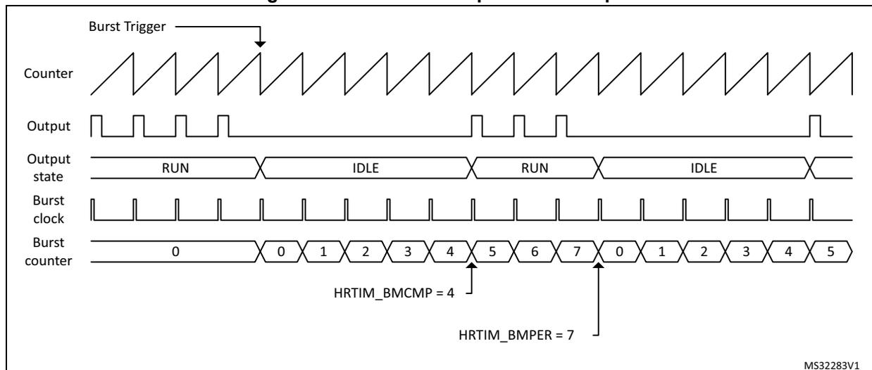
The figure illustrates the timing relationship in burst mode. - Burst Trigger : An external or internal event that initiates the burst sequence. - Counter : A standard sawtooth waveform representing the timer counter. - Output : Shows PWM pulses during the RUN state and remains at a constant level during the IDLE state. - Output state : A logic signal indicating whether the system is in the RUN or IDLE phase. - Burst clock : A periodic clock signal used by the burst controller. - Burst counter : Increments with the Burst clock. It resets to 0 at the start of an IDLE period. - HRTIM_BMCMP = 4 : Indicates that the transition from IDLE to RUN occurs when the burst counter reaches 4. - HRTIM_BMPER = 7 : Indicates the total period of the burst cycle (from 0 to 7), after which the counter resets to 0 and a new IDLE period begins.
The burst mode controller consists of:
- • A counter that can be clocked by various sources, either within or outside the HRTIM (typically the end of a PWM period).
- • A compare register to define the number of idle periods: HRTIM_BMCMP.
- • A period register to define the burst repetition rate (corresponding to the sum of the idle and run periods): HRTIM_BMPER.
The burst mode controller is able to take over the control of any of the 10 PWM outputs. The state of each output during a burst mode operation is programmed using IDLESx and IDLEMx bits in the HRTIM_OUTxR register, as in Table 250 .
Table 250. Timer output programming for burst mode
| IDLEMx | IDLESx | Output state during burst mode |
|---|---|---|
| 0 | X | No action: the output is not affected by the burst mode operation. |
| 1 | 0 | Output inactive during the burst |
| 1 | 1 | Output active during the burst |
Note: IDLEMx bit must not be changed while the burst mode is active.
The burst mode controller only acts on the output stage. A number of events are still generated during the idle period:
- • Output set/reset interrupt or DMA requests
- • External event filtering based on Tx2 output signal
- • Capture events triggered by output set/reset
During the burst mode, neither start nor reset events are generated on the hrtim_out_sync[2:1] output, even if TxBM bit is set.
Operating mode
It is necessary to have the counter enabled (TxCEN bit set) before using the burst mode on a given timing unit. The burst mode is enabled with BME bit in the HRTIM_BMCR register.
It can operate in continuous or single-shot mode, using BMOM bit in the HRTIM_BMCR register. The continuous mode is enabled when BMOM = 1. The burst operation is maintained until BMSTAT bit in HRTIM_BMCR is reset to terminate it.
In single-shot mode (BMOM = 0), the idle sequence is executed once, following the burst mode trigger, and the normal timer operation is resumed immediately after.
The duration of the idle and run periods is defined with a burst mode counter and 2 registers. The HRTIM_BMCMPR register defines the number of counts during which the selected timer(s) are in an idle state (idle period). HRTIM_BMPER defines the overall burst mode period (sum of the idle and run periods). Once the initial burst mode trigger has occurred, the idle period length is HRTIM_BMCMPR+1, the overall burst period is HRTIM_BMPER+1.
Note: The burst mode period must not be less than or equal to the deadtime duration defined with DTRx[8:0] and DTFx[8:0] bitfields.
The counters of the timing units and the master timer can be stopped and reset during the burst mode operation. HRTIM_BMCR holds 6 control bits for this purpose: MTBM (master) and TABM..TEBM for timer A..E.
When MTBM or TxBM bit is reset, the counter clock is maintained. This allows to keep a phase relationship with other timers in multiphase systems, for instance.
When MTBM or TxBM bit is set, the corresponding counter is stopped and maintained in reset state during the burst idle period. This allows to have the timer restarting a full period when exiting from idle. If SYNCSRC[1:0] = 00 or 10 (synchronization output on the master
start or timer A start), a pulse is sent on the HRTIM_SCOUT output when exiting the burst mode.
Note: TxBM bit must not be set when the balanced idle mode is active (DLYPRT[1:0] = 0x11).
Burst mode clock
The burst mode controller counter can be clocked by several sources, selected with BMCLK[3:0] bits in the HRTIM_BMCR register:
- • BMCLK[3:0] = 0000 to 0101: master timer and TIMA..E reset/roll-over events. This allows to have burst mode idle and run periods aligned with the timing unit counting period (both in free-running and counter reset mode).
- • BMCLK[3:0] = 0110 to 1001: The clocking is provided by the hrtim_bm_ck[4:1] inputs connected to general purpose timers, as in Table 225 . In this case, the burst mode idle and run periods are not necessarily aligned with timing unit counting period (a pulse on the output may be interrupted, resulting a waveform with modified duty cycle for instance).
- • BMCLK[3:0] = 1010: The \( f_{HRTIM} \) clock prescaled by a factor defined with BMPRSC[3:0] bits in HRTIM_BMCR register. In this case, the burst mode idle and run periods are not necessarily aligned with the timing unit counting period (a pulse on the output may be interrupted, resulting in a waveform with a modified duty cycle, for instance).
The pulse width on TIMx OC output must be at least N \( f_{HRTIM} \) clock cycles long to be detected by the HRTIM burst mode controller.
Burst mode triggers
To trigger the burst operation, 32 sources are available and are selected using the HRTIM_BMTRGR register:
- • Software trigger (set by software and reset by hardware)
- • 6 master timer events: repetition, reset/roll-over, compare 1 to 4
- • 5 x 4 events from timers A..F: repetition, reset/roll-over, compare 1 and 2
- • External event 7 (including TIMA event filtering) and 8 (including TIMD event filtering)
- • Timer A period following external event 7 (including TIMA event filtering)
- • Timer D period following external event 8 (including TIMD event filtering)
- • An on-chip event on the hrtim_bm_trg input (connected to the general-purpose timer TRGO output), see Table 222 for details.
These sources can be combined to have multiple concurrent triggers.
Burst mode is not re-triggerable. In continuous mode, new triggers are ignored until the burst mode is terminated, while in single-shot mode, the triggers are ignored until the current burst completion including run periods (HRTIM_BMPER+1 cycles). This is also valid for software trigger (the software bit is reset by hardware even if it is discarded).
Figure 264 shows how the burst mode is started in response to an external event, either immediately or on the timer period following the event.
Figure 264. Burst mode trigger on external event
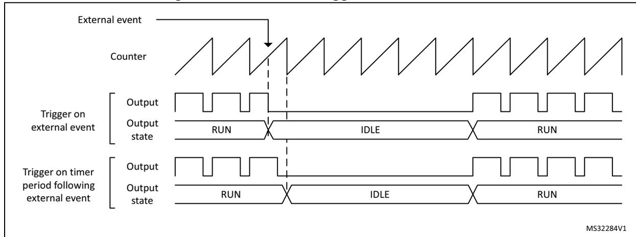
For TAEEV7 and TDEEV8 combined triggers (trigger on a timer period following an external event), the external event detection is always active, regardless of the burst mode programming and the on-going burst operation:
- • When the burst mode is enabled (BME=1) or the trigger is enabled (TAEEV7 or TDEEV8 bit set in the BMTRG register) in between the external event and the timer period event, the burst is triggered.
- • The single-shot burst mode is re-triggered even if the external event occurs before the burst end (as long as the corresponding period happens after the burst).
Note: TAEEV7 and TDEEV8 triggers are valid only after a period event. If the counter is reset before the period event, the pending hrtim_eev7 or hrtim_eev8 event is discarded.
Burst mode delayed entry
By default, the outputs are taking their idle level (as per IDLES1 and IDLES2 setting) immediately after the burst mode trigger.
It is also possible to delay the burst mode entry and force the output to an inactive state during a programmable period before the output takes its idle state. This is useful when driving two complementary outputs, one of them having an active idle state, to avoid a deadtime violation as shown on Figure 265 . This prevents any risk of shoot through current in half-bridges, but causes a delayed response to the burst mode entry.
Figure 265. Delayed burst mode entry with deadtime enabled and IDLESx = 1
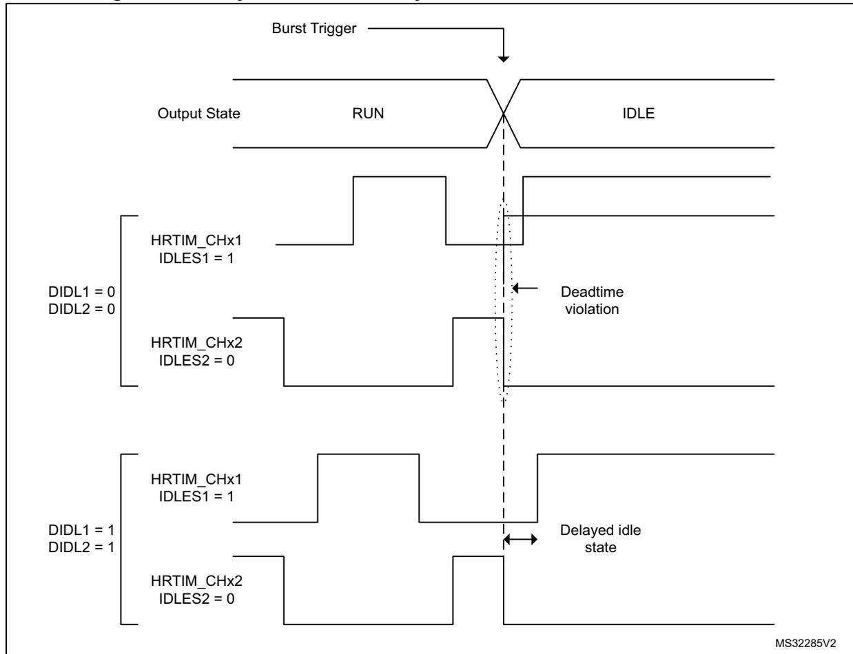
The diagram shows the timing of HRTIM outputs during a burst mode entry. A 'Burst Trigger' signal initiates the transition from 'RUN' to 'IDLE' state. The diagram is divided into two sections based on the configuration of the
DIDLx
bits in the
HRTIM_OUTxR
register.
- Top Section (DIDL1 = 0, DIDL2 = 0):
- HRTIM_CHx1 (IDLES1 = 1): The output transitions from RUN to IDLE. A 'Deadtime violation' is indicated by a dashed line and an arrow pointing to the transition point.
- HRTIM_CHx2 (IDLES2 = 0): The output transitions from RUN to IDLE. No deadtime violation is indicated.
- Bottom Section (DIDL1 = 1, DIDL2 = 1):
- HRTIM_CHx1 (IDLES1 = 1): The output transitions from RUN to IDLE. A 'Delayed idle state' is indicated by a double-headed arrow pointing to the transition point.
- HRTIM_CHx2 (IDLES2 = 0): The output transitions from RUN to IDLE. No deadtime violation is indicated.
The diagram illustrates that when
DIDLx = 1
and
IDLESx = 1
, a deadtime insertion is enforced before the output takes its idle state, resulting in a 'Delayed idle state'. When
DIDLx = 0
, no deadtime insertion is enforced, which can lead to a 'Deadtime violation' if the output transitions too quickly.
MS32285V2
The delayed burst entry mode is enabled with
DIDLx
bit in the
HRTIM_OUTxR
register (one enable bit per output). It forces a deadtime insertion before the output takes its idle state. Each
TIMx
output has its own deadtime value:
- –
DTRx[8:0]on output 1 whenDIDL1 = 1 - –
DTFx[8:0]on output 2 whenDIDL2 = 1
DIDLx
bits can be set only if one of the outputs has an active idle level during the burst mode (
IDLES = 1
) and only when positive deadtimes are used (
SDTR/SDTF
set to 0).
Note:
The delayed burst entry mode uses deadtime generator resources. Consequently, when any of the 2
DIDLx
bits is set and the corresponding timing unit uses the deadtime insertion (
DTEN
bit set in
HRTIM_OUTxR
), it is not possible to use the
timerx
output 2 as a filter for external events (
Tx2
filtering signal is not available).
When durations defined by
DTRx[8:0]
and
DTFx[8:0]
are lower than 3
\(
f_{HRTIM}
\)
clock cycle periods, the limitations related to the narrow pulse management listed in
Section 28.3.7
must be applied.
When the burst mode entry arrives during the regular deadtime, it is aborted and a new deadtime is re-started corresponding to the inactive period, as on Figure 266 .
Figure 266. Delayed burst mode entry during deadtime
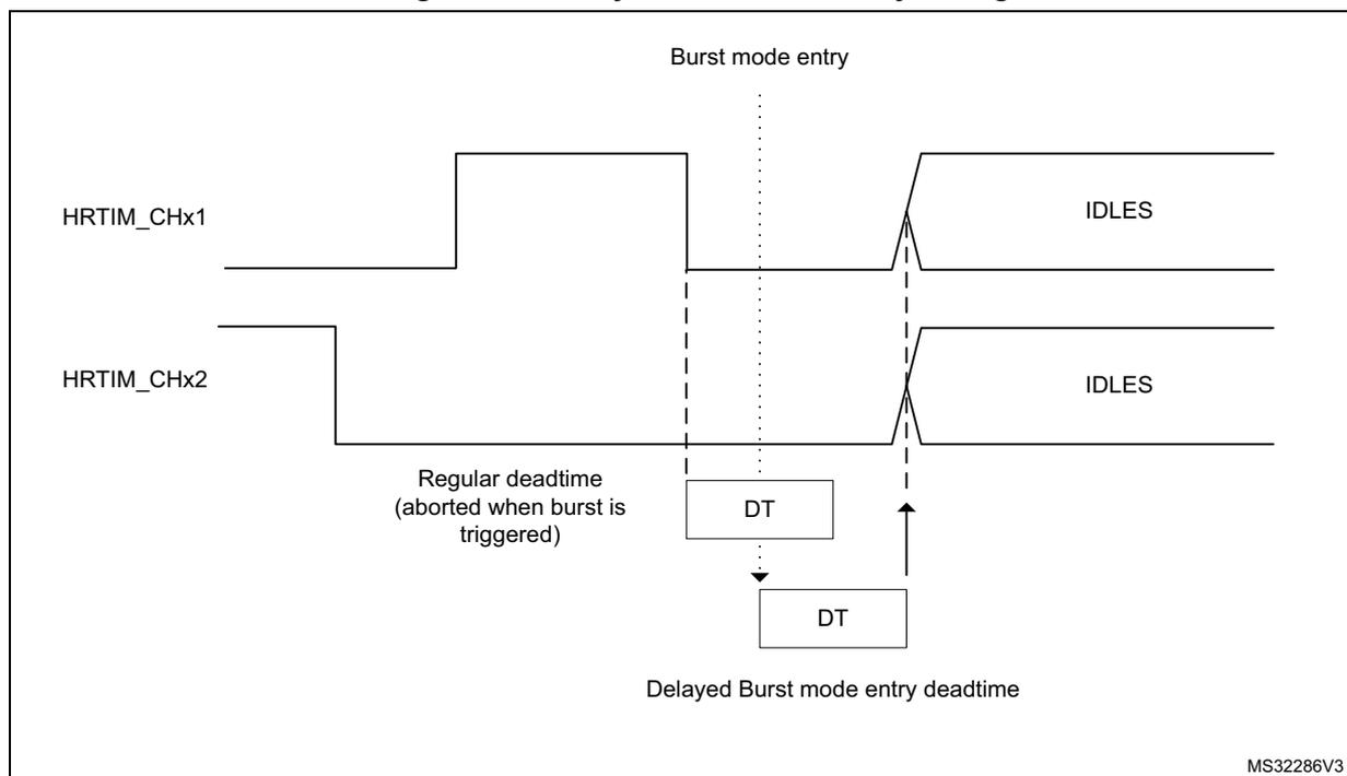
The diagram shows two output waveforms, HRTIM_CHx1 and HRTIM_CHx2. Both start in an active state (high for CHx1, low for CHx2). A vertical dashed line marks the 'Burst mode entry' point. At this point, the 'Regular deadtime (aborted when burst is triggered)' is shown as a short interval. Below this, a 'Delayed Burst mode entry deadtime' is shown as a longer interval. After the deadtime, both outputs transition to an 'IDLES' state. The label 'MS32286V3' is in the bottom right corner.
Burst mode exit
The burst mode exit is either forced by software (in continuous mode) or once the idle period is elapsed (in single-shot mode). In both cases, the counter is re-started immediately (if it was hold in a reset state with MTBM or TxBM bit = 1), but the effective output state transition from the idle to active mode only happens after the programmed set/reset event.
A burst period interrupt is generated in single-shot and continuous modes when BMPERIE enable bit is set in the HRTIM_IER register. This interrupt can be used to synchronize the burst mode exit with a burst period in continuous burst mode.
Figure 267 shows how a normal operation is resumed when the deadtime is enabled. Although the burst mode exit is immediate, this is only effective on the first set event on any of the complementary outputs.
Two different cases are presented:
- 1. The burst mode ends while the signal is inactive on the crossbar output waveform. The active state is resumed on Tx1 and Tx2 on the set event for the Tx1 output, and the Tx2 output does not take the complementary level on burst exit.
- 2. The burst mode ends while the crossbar output waveform is active: the activity is resumed on the set event of Tx2 output, and Tx1 does not take the active level immediately on burst exit.
Figure 267. Burst mode exit when the deadtime generator is enabled
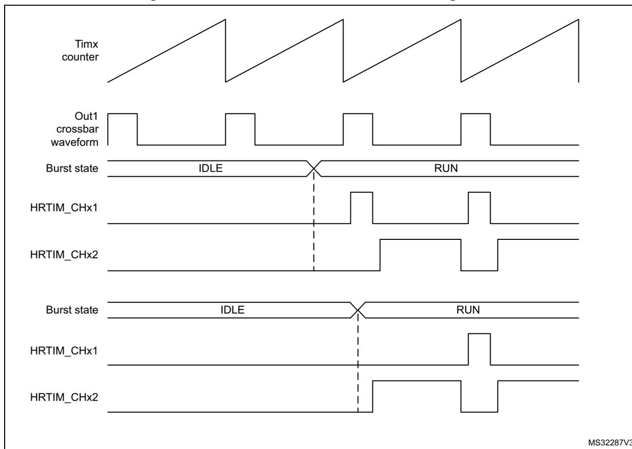
The figure is a timing diagram illustrating the behavior of an HRTIM timer in burst mode when the deadtime generator is enabled. It consists of two main sections, each showing a different output configuration.
- Top Section:
- Timx counter: A sawtooth waveform that increases linearly and then resets.
- Out1 crossbar waveform: A square wave that is high during the IDLE state and low during the RUN state.
- Burst state: A signal that transitions from IDLE to RUN at a specific point in time, marked by a vertical dashed line.
- HRTIM_CHx1: An output that is high during the IDLE state and becomes low upon entering the RUN state.
- HRTIM_CHx2: An output that is low during the IDLE state and becomes high upon entering the RUN state.
- Bottom Section:
- Burst state: Similar to the top section, it transitions from IDLE to RUN.
- HRTIM_CHx1: An output that is low during the IDLE state and becomes high upon entering the RUN state.
- HRTIM_CHx2: An output that is high during the IDLE state and becomes low upon entering the RUN state.
The vertical dashed lines indicate the transition points between the IDLE and RUN states. The diagram shows that the outputs are reset or forced to a specific state at the beginning of the RUN period, depending on their configuration.
MS32287V3
The behavior described above is slightly different when the push-pull mode is enabled. The push-pull mode forces an output reset at the beginning of the period if the output is inactive, or symmetrically forces an active level if the output was high during the preceding period.
Consequently, an output with an active idle state can be reset at the time the burst mode is exited even if no transition is explicitly programmed. For symmetrical reasons, an output can be set at the time the burst mode is exited even if no transition is explicitly programmed, in case it was active when it entered in idle state.
Burst mode registers preloading and update
BMPREN bit (burst mode preload enable) allows to have the burst mode compare and period registers preloaded (HRTIM_BMCMP and HRTIM_BMPER).
When BMPREN is set, the transfer from preload to active register happens:
- • when the burst mode is enabled (BME = 1),
- • at the end of the burst mode period.
A write into the HRTIM_BMPER period register disables the update temporarily, until the HRTIM_BMCMP compare register is written, to ensure the consistency of the two registers when they are modified.
If the compare register only needs to be changed, a single write is necessary. If the period only needs to be changed, it is also necessary to re-write the compare to have the new values taken into account.
When BMPREN bits is reset, the write access into BMCMR and BMPER directly updates the active register. In this case, it is necessary to consider when the update is done during the overall burst period, for the 2 cases below:
a) Compare register update
If the new compare value is above the current burst mode counter value, the new compare is taken into account in the current period.
If the new compare value is below the current burst mode counter value, the new compare is taken into account in the next burst period in continuous mode, and ignored in single-shot mode (no compare match occurs and the idle state lasts until the end of the idle period).
b) Period register update
If the new period value is above the current burst mode counter value, the change is taken into account in the current period.
Note: If the new period value is below the current burst mode counter value, the new period is not taken into account, the burst mode counter overflows (at 0xFFFF) and the change is effective in the next period. In single-shot mode, the counter rolls over at 0xFFFF and the burst mode re-starts for another period up to the new programmed value.
Burst mode emulation using a compound register
The burst mode controller only controls one or a set of timers for a single converter. When the burst mode is necessary for multiple independent timers, it is possible to emulate a simple burst mode controller using the DMA and the HRTIM_CMP1CxR compound register, which holds aliases of both the repetition and the compare 1 registers.
This is applicable to a converter which only requires a simple PWM (typically a buck converter), where the duty cycle only needs to be updated. In this case, the CMP1 register is used to reset the output (and define the duty cycle), while it is set on the period event.
In this case, a single 32-bit write access in CMP1CxR is sufficient to define the duty cycle (with the CMP1 value) and the number of periods during which this duty cycle is maintained (with the repetition value). To implement a burst mode, it is then only necessary to transfer by DMA (upon repetition event) two 32-bit data in continuous mode, organized as follows:
CMP1CxR = {REP_Idle; CMP1 = Duty_Cycle}, {REP_Run; CMP1 = 0}
For instance, the values:
{0x0001 0000}: CMP1 = 0 for 2 periods during Idle
{0x0003 0800}: CMP1 = 0x0800 for 4 periods during Run
provide a burst mode with 2 periods active every 6 PWM periods, as shown on Figure 268 .
Figure 268. Burst mode emulation example
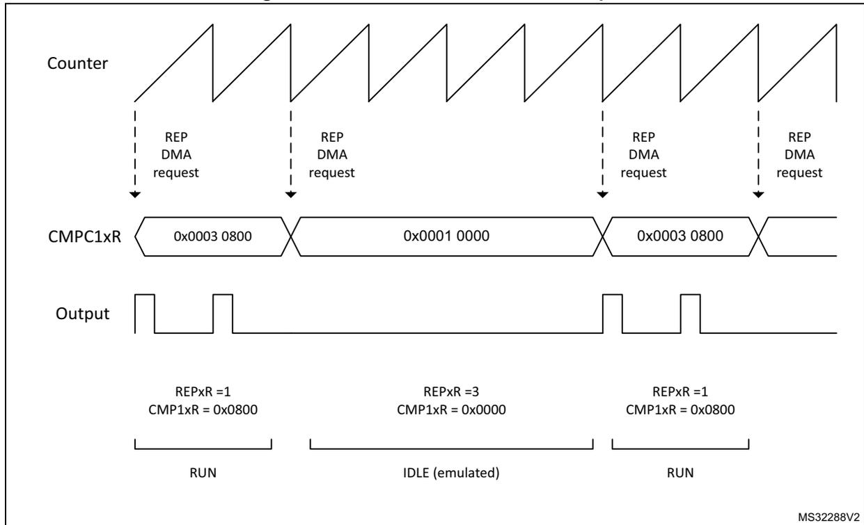
The diagram illustrates burst mode emulation using the HRTIM. It consists of three horizontal timelines:
- Counter: Shows a sawtooth waveform representing the counter value. Vertical dashed lines indicate 'REP DMA request' events at the end of each counter cycle.
- CMPC1xR:
Shows the value of the CMPC1xR register. It is divided into three segments:
- First segment: Value 0x0003 0800. Below it, text indicates REPxR = 1 and CMPC1xR = 0x0800. This segment corresponds to the 'RUN' state.
- Second segment: Value 0x0001 0000. Below it, text indicates REPxR = 3 and CMPC1xR = 0x0000. This segment corresponds to the 'IDLE (emulated)' state.
- Third segment: Value 0x0003 0800. Below it, text indicates REPxR = 1 and CMPC1xR = 0x0800. This segment corresponds to the 'RUN' state.
- Output: Shows the output signal waveform. It is a pulse train that is active during the 'RUN' segments and inactive (low) during the 'IDLE (emulated)' segment.
MS32288V2
28.3.16 Chopper
A high-frequency carrier can be added on top of the timing unit output signals to drive isolation transformers. This is done in the output stage before the polarity insertion, as shown on Figure 269, using CHP1 and CHP2 bits in the HRTIM_OUTxR register, to enable chopper on outputs 1 and 2, respectively.
Figure 269. Carrier frequency signal insertion
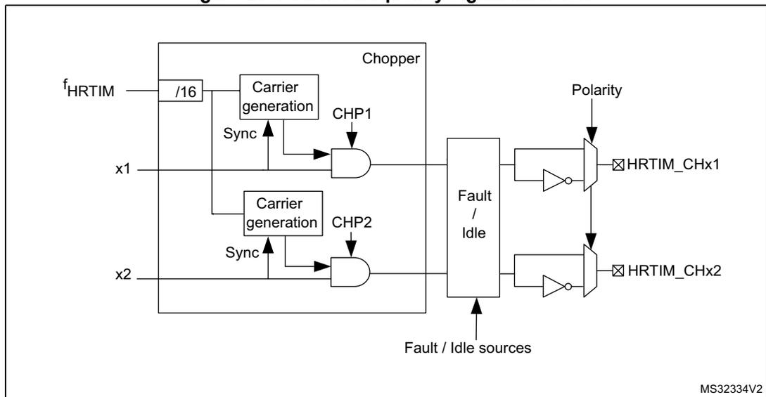
The diagram shows the internal logic for carrier frequency insertion into the HRTIM outputs. Key components include:
- Chopper: A large block containing two 'Carrier generation' units. The first unit takes the HRTIM clock ( \( f_{HRTIM} \) ) divided by 16 and a 'Sync' signal to generate a carrier for CHP1. The second unit does the same for CHP2. The outputs of these carriers are ANDed with the main HRTIM signals (x1 and x2).
- Fault / Idle: A block that receives 'Fault / Idle sources' and controls the output stage.
- Polarity: A control input for the output drivers.
- Outputs: The final output signals are HRTIM_CHx1 and HRTIM_CHx2, which are the result of the AND operations and subsequent polarity insertion.
MS32334V2
The chopper parameters can be adjusted using the HRIM_CHPxR register, with the possibility to define a specific pulsewidth at the beginning of the pulse, to be followed by a carrier frequency with programmable frequency and duty cycle, as in Figure 270 .
CARFRQ[3:0] bits define the frequency, ranging from 664 kHz to 10.625 MHz (for \( f_{HRTIM} = 170 \text{ MHz} \) ) following the formula \( F_{CHPFRQ} = f_{HRTIM} / (16 \times (CARFRQ[3:0]+1)) \) .
The duty cycle can be adjusted by 1/8 step with CARDTY[2:0], from 0/8 up to 7/8 duty cycle. When CARDTY[2:0] = 000 (duty cycle = 0/8), the output waveform only contains the starting pulse following the rising edge of the reference waveform, without any added carrier.
The pulsewidth of the initial pulse is defined using the STRPW[3:0] bitfield as follows: \( t_{1STPW} = (STRPW[3:0]+1) \times 16 \times t_{HRTIM} \) and ranges from 94.1 ns to 1.51 µs (for \( f_{HRTIM} = 170 \text{ MHz} \) ).
The carrier frequency parameters are defined based on the \( f_{HRTIM} \) frequency, and are not dependent from the CKPSC[2:0] setting.
In chopper mode, the carrier frequency and the initial pulsewidth are combined with the reference waveform using an AND function. A synchronization is performed at the end of the initial pulse to have a repetitive signal shape.
The chopping signal is stopped at the end of the output waveform active state, without waiting for the current carrier period to be completed. It can thus contain shorter pulses than programmed.
Figure 270. HRTIM outputs with Chopper mode enabled
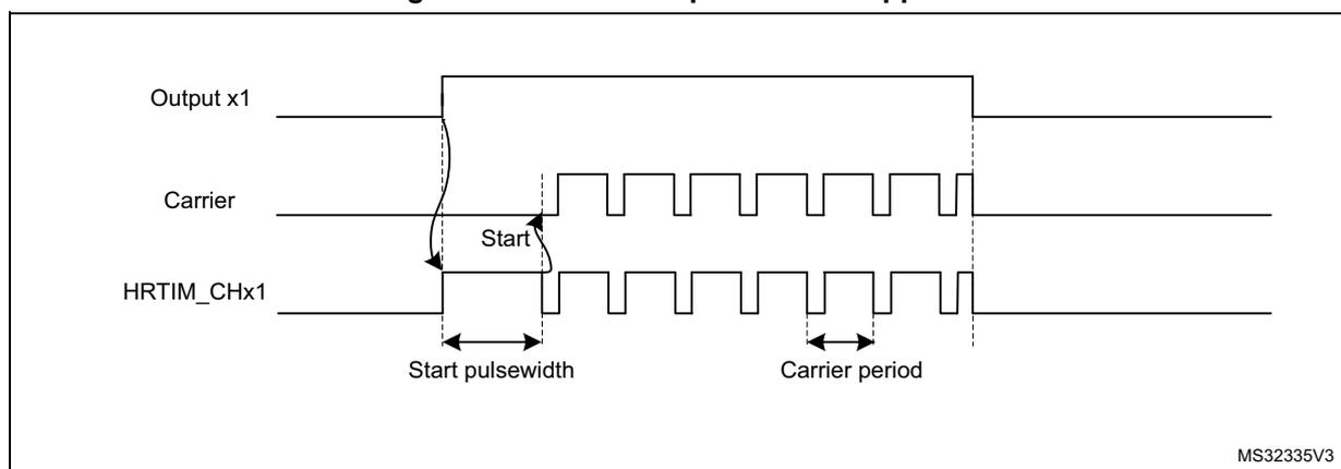
Note: CHP1 and CHP2 bits must be set prior to the output enable done with TxyOEN bits in the HRTIM_OENR register.
CARFRQ[2:0], CARDTY[2:0] and STRPW[3:0] bitfields cannot be modified while the chopper mode is active (at least one of the two CHPx bits is set).
28.3.17 Fault protection
The HRTIM has a versatile fault protection circuitry to disable the outputs in case of an abnormal operation. Once a fault has been triggered, the outputs take a predefined safe state. This state is maintained until the output is re-enabled by software. In case of a permanent fault request, the output remains in its fault state, even if the software attempts to re-enable them, until the fault source disappears.
The HRTIM has 6 FAULT input channels; all of them are available and can be combined for each of the 6 timing units, as shown on Figure 271 .
Figure 271. Fault protection circuitry (FAULT1 fully represented, FAULT2..6 partially)
![Figure 271: Fault protection circuitry diagram. The diagram shows the internal logic for fault protection in an HRTIM. At the top, 'Timer x' is connected to two comparators. The first comparator takes 'FAULT1[1:0]' as input and its output is connected to 'HRTIM_CHx1'. The second comparator takes 'FAULT2[1:0]' as input and its output is connected to 'HRTIM_CHx2'. Below the timers, a 'Counter' block is shown with inputs 'FLT1RSTM' and 'FLT1CREG'. It has two feedback loops: one through a switch labeled 'FLT1P' and another through a block labeled 'FLT1CNT[3:0]'. The 'Counter' output is connected to a 'Filter' block. The 'Filter' block has inputs 'FLT1SRC[1:0]' (selecting between 'HRTIM_FLT[1]', 'hrtim_in_flt1', 'EEV1_muxout', and 'N/A'), 'FLT1P' (polarity), and 'fILTERS FLT1F[3:0]' (filter length). The 'Filter' output is connected to a 'Blanking sources' block. The 'Blanking sources' block output is connected to a 'SYSFLT' block, which outputs 'hrtim_sys_flt'. The 'SYSFLT' output is also connected to a series of AND gates. The first AND gate takes 'FLT1E' and 'Fault2' as inputs. The second AND gate takes 'FLT2EN' and 'Fault3' as inputs. The third AND gate takes 'FLT3EN' and 'Fault4' as inputs. The outputs of these AND gates are connected to a 3-input OR gate, which outputs 'Fault 6', 'Fault 5', and 'Fault 4'. The 'SYSFLT' output is also connected to the 'FLT1CNT[3:0]' block.](/RM0440-STM32G4/d7c046caff249c338369403bb7f825ce_img.jpg)
Each fault channel is fully configurable using HRTIM_FLTINR1 and HRTIM_FLTINR2 registers before being routed to the timing units. FLTxSRC FLTxSRC[1:0] bit selects the source of the fault signal, that can be either a digital input or an internal event (built-in comparator output).
Table 228 details the 3 available sources for each of the 6 faults channels.
The EEVx_muxout event mentioned in Figure 271 above is taken after the hrtim_eevx[4:1] input multiplexer controlled by the EExSRC[1:0] bits. Refer to Figure 243 for details.
The polarity of the signal can be selected to define the active level, using the FLTxP polarity bit in HRTIM_FLTINRx registers. If FLTxP = 0, the signal is active at low level; if FLTxP = 1, it is active when high.
The fault information can be filtered after the polarity setting. If FLTxF[3:0] bitfield is set to 0000, the signal is not filtered and acts asynchronously, independently from the \( f_{HRTIM} \) clock. For all other FLTxF[3:0] bitfield values, the signal is digitally filtered. The digital filter is made of a counter in which a number N of valid samples is needed to validate a transition on the output. If the input value changes before the counter has reached the value N, the counter is reset and the transition is discarded (considered as a spurious event). If the counter reaches N, the transition is considered as valid and transmitted as a correct external event. Consequently, the digital filter adds a latency to the external events being filtered, depending on the sampling clock and on the filter length (number of valid samples expected). Figure 272 shows how a spurious fault signal is filtered.
Figure 272. Fault signal filtering (FLTxF[3:0] = 0010:\( f_{\text{SAMPLING}} = f_{\text{HRTIM}} \) , N = 4)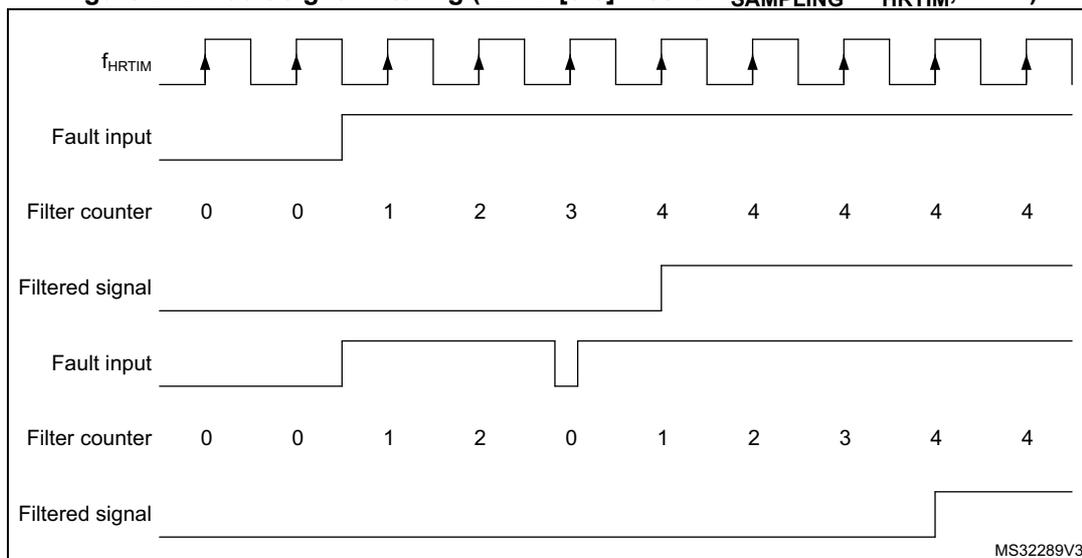
The filtering period ranges from 2 cycles of the \( f_{\text{HRTIM}} \) clock up to 8 cycles of the \( f_{\text{FLTS}} \) clock divided by 32. \( f_{\text{FLTS}} \) is defined using FLTSD[1:0] bits in the HRTIM_FLTINR2 register.
Table 251 summarizes the sampling rate and the filter length. A jitter of 1 sampling clock period must be subtracted from the filter length to take into account the uncertainty due to the sampling and have the effective filtering.
Table 251. Sampling rate and filter length vs FLTxF[3:0] and clock setting
| - | \( f_{\text{FLTS}} \) vs FLTSD[1:0] | Filter length for \( f_{\text{HRTIM}} = 170 \text{ MHz} \) | |||||
|---|---|---|---|---|---|---|---|
| FLTxF[3:0] | 00 | 01 | 10 | 11 | Min | Max | |
| 0001,0010,0011 | \( f_{\text{HRTIM}} \) | \( f_{\text{HRTIM}} \) | \( f_{\text{HRTIM}} \) | \( f_{\text{HRTIM}} \) | \(
f_{\text{HRTIM}}
\)
, N = 2 11.8 ns | \(
f_{\text{HRTIM}}
\)
, N = 8 47.1 ns | |
| 0100, 0101 | \( f_{\text{HRTIM}} / 2 \) | \( f_{\text{HRTIM}} / 4 \) | \( f_{\text{HRTIM}} / 8 \) | \( f_{\text{HRTIM}} / 16 \) | \(
f_{\text{HRTIM}} / 2
\)
, N = 6 70.6 ns | \(
f_{\text{HRTIM}} / 16
\)
, N = 8 753 ns | |
| 0110, 0111 | \( f_{\text{HRTIM}} / 4 \) | \( f_{\text{HRTIM}} / 8 \) | \( f_{\text{HRTIM}} / 16 \) | \( f_{\text{HRTIM}} / 32 \) | \(
f_{\text{HRTIM}} / 4
\)
, N = 6 141 ns | \(
f_{\text{HRTIM}} / 32
\)
, N = 8 1.51 \( \mu\text{s} \) | |
| 1000, 1001 | \( f_{\text{HRTIM}} / 8 \) | \( f_{\text{HRTIM}} / 16 \) | \( f_{\text{HRTIM}} / 32 \) | \( f_{\text{HRTIM}} / 64 \) | \(
f_{\text{HRTIM}} / 8
\)
, N = 6 282 ns | \(
f_{\text{HRTIM}} / 64
\)
, N = 8 3.01 \( \mu\text{s} \) | |
| 1010, 1011, 1100 | \( f_{\text{HRTIM}} / 16 \) | \( f_{\text{HRTIM}} / 32 \) | \( f_{\text{HRTIM}} / 64 \) | \( f_{\text{HRTIM}} / 128 \) | \(
f_{\text{HRTIM}} / 16
\)
, N = 5 471 ns | \(
f_{\text{HRTIM}} / 128
\)
, N = 8 6.02 \( \mu\text{s} \) | |
| 1101, 1110, 1111 | \( f_{\text{HRTIM}} / 32 \) | \( f_{\text{HRTIM}} / 64 \) | \( f_{\text{HRTIM}} / 128 \) | \( f_{\text{HRTIM}} / 256 \) | \(
f_{\text{HRTIM}} / 32
\)
, N = 5 941 ns | \(
f_{\text{HRTIM}} / 256
\)
, N = 8 12.05 \( \mu\text{s} \) | |
Fault blanking and event counting
The fault inputs can be temporarily disabled to blank spurious fault events. The blanking sources are listed in the Table 252 below.
Table 252. Fault input blanking events
| Fault input | FLTxBLS = 0, reset-aligned window | FLTxBLS = 1 moving window | ||
|---|---|---|---|---|
| Blanking window start | Blanking window end | Blanking window start | Blanking window end | |
| Fault 1 | Timer A reset/roll-over | Timer A CMP3 event | Timer A CMP4 event | Timer A CMP3 event |
| Fault 2 | Timer B reset/roll-over | Timer B CMP3 event | Timer B CMP4 event | Timer B CMP3 event |
| Fault 3 | Timer C reset/roll-over | Timer C CMP3 event | Timer C CMP4 event | Timer C CMP3 event |
| Fault 4 | Timer D reset/roll-over | Timer D CMP3 event | Timer D CMP4 event | Timer D CMP3 event |
| Fault 5 | Timer E reset/roll-over | Timer E CMP3 event | Timer E CMP4 event | Timer E CMP3 event |
| Fault 6 | Timer F reset/roll-over | Timer F CMP3 event | Timer F CMP4 event | Timer F CMP3 event |
A fault counter also allows to discard multiple spurious fault events and define an acceptance criteria.
The FLTxCNT[3:0] bitfield selects the FAULTx counter threshold. A fault is considered valid when the number of events is equal to the FLTxCNT[3:0] value.
This FLTxRSTM selects the FAULTx counter reset mode
- • 0: fault counter hardware reset on reset / roll-over event, as per the Table 253 below.
- • 1: fault counter reset on each reset / roll-over event only if no event occurs during last counting period, as shown on Figure 273 below.
The fault counter can be reset by software with the FLTxCRES bit at anytime.
Figure 273. Fault counter cumulative mode (FLTxRSTM = 1, FLTxCNT[3:0] = 2)
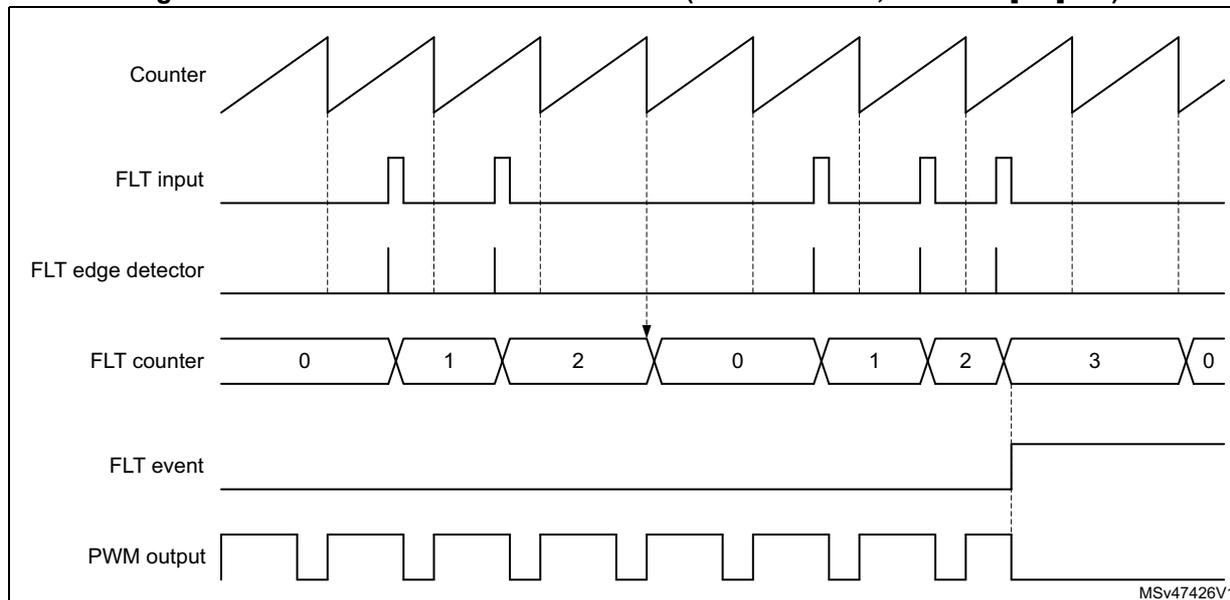
The diagram shows the following signal levels and transitions:
- Counter: A sawtooth waveform representing the main timer counter. It resets to 0 upon roll-over.
- FLT input: A signal with several rising edges. Some edges occur during the counter's active period, while others occur just after a roll-over.
- FLT edge detector: Generates a narrow pulse on each rising edge of the FLT input.
- FLT counter: A counter that increments by 1 on each rising edge of the FLT input. It resets to 0 when the main Counter rolls over. The sequence of values shown is 0, 1, 2, 0, 1, 2, 3, 0. A threshold of 2 is indicated.
- FLT event: A pulse that goes high when the FLT counter reaches the threshold value of 2 and remains high until the next Counter roll-over.
- PWM output: A square wave that is affected by the FLT event. When the FLT event is high, the PWM output is forced to a specific state.
A given FLTx input counter can be reset by a single source. The Table 253 indicates which timer unit associated with a given fault. This does not prevent to have a fault line shared by multiple timer (e.g. FLT1 with event counter enabled, acting on timer A, timer B and timer C simultaneously).
Table 253. Fault 1..6 counter reset source| Fault Input | Fault counter reset source |
|---|---|
| Fault 1 | Timer A reset/roll-over |
| Fault 2 | Timer B reset/roll-over |
| Fault 3 | Timer C reset/roll-over |
| Fault 4 | Timer D reset/roll-over |
| Fault 5 | Timer E reset/roll-over |
| Fault 6 | Timer F reset/roll-over |
This input overrides the FAULT inputs and disables all outputs having FAULTy[1:0] = 01, 10, 11. Refer to Table 230 for the list of system faults connected to this input.
For each FAULT channel, a write-once FLTxLCK bit in the HRTIM_FLTxR register allows to lock FLTxE, FLTxP, FLTxSRC, FLTxF[3:0] bits (it renders them read-only), for functional safety purpose. If enabled, the fault conditioning set-up is frozen until the next HRTIM or system reset.
Once the fault signal is conditioned as explained above, it is routed to the timing units. For any of them, the 6 fault channels are enabled using bits FLT1EN to FLT6EN in the HRTIM_FLTxR register, and they can be selected simultaneously (the sysfault is automatically enabled as long as the output is protected by the fault mechanism). This allows to have, for instance:
- • One fault channel simultaneously disabling several timing units
- • Multiple fault channels being ORed to disable a single timing unit
A write-once FLTLOCK bit in the HRTIM_FLTxR register allows to lock FLTxEN bits (it renders them read-only) until the next reset, for functional safety purpose. If enabled, the timing unit fault-related set-up is frozen until the next HRTIM or system reset.
For each of the timers, the output state during a fault is defined with FAULT1[1:0] and FAULT2[1:0] bits in the HRTIM_OUTxR register (see Section 28.3.14 ).
28.3.18 Auxiliary outputs
Timer A to E have auxiliary outputs in parallel with the regular outputs going to the output stage. They provide the following internal status, events and signals:
- • SETxy and RSTxy status flags, together with the corresponding interrupts and DMA requests
- • Capture triggers upon output set/reset
- • External event filters following a Tx2 output copy (see details in Section 28.3.9 )
The auxiliary outputs are taken either before or after the burst mode controller, depending on the HRTIM operating mode. An overview is given on Figure 274 .
Figure 274. Auxiliary outputs
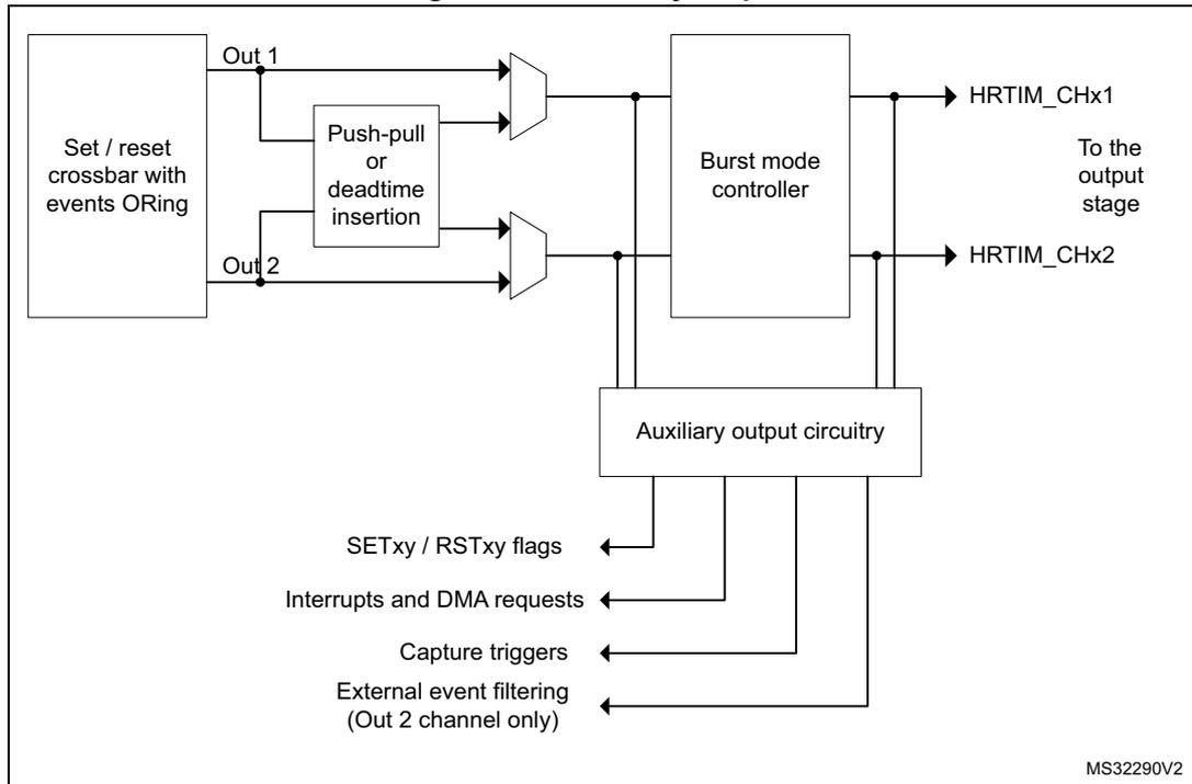
The diagram shows the signal flow for auxiliary outputs. It starts with a block labeled 'Set / reset crossbar with events ORing' which has two outputs, 'Out 1' and 'Out 2'. These signals enter a 'Push-pull or deadtime insertion' block. The outputs from this block, along with the original 'Out 1' and 'Out 2' signals, are multiplexed. The resulting signals pass through a 'Burst mode controller' to become 'HRTIM_CHx1' and 'HRTIM_CHx2', which go 'To the output stage'. Additionally, there is an 'Auxiliary output circuitry' block that takes inputs from the signals before and after the burst mode controller and generates several signals: 'SETxy / RSTxy flags', 'Interrupts and DMA requests', 'Capture triggers', and 'External event filtering (Out 2 channel only)'.
By default, the auxiliary outputs are copies of outputs Tx1 and Tx2. The exceptions are:
- • The delayed idle and the balanced idle protections, when the deadtime is disabled ( \( DTEN = 0 \) ). When the protection is triggered, the auxiliary outputs are maintained and follow the signal coming out of the crossbar. On the contrary, if the deadtime is enabled ( \( DTEN = 1 \) ), both main and auxiliary outputs are forced to an inactive level.
- • The burst mode (
\(
TCEN=1
\)
,
\(
IDLEMx=1
\)
); there are 2 cases:
- a) If \( DTEN=0 \) or \( DIDLx=0 \) , the auxiliary outputs are not affected by the burst mode entry and continue to follow the reference signal coming out of the crossbar (see Figure 275 ).
- b) If the deadtime is enabled ( \( DTEN=1 \) ) together with the delayed burst mode entry ( \( DIDLx=1 \) ), the auxiliary outputs have the same behavior as the main outputs. They are forced to the IDLES level after a deadtime duration, then they keep this level during all the burst period. When the burst mode is terminated, the IDLES level is maintained until a transition occurs to the opposite level, similarly to the main output.
Figure 275. Auxiliary and main outputs during burst mode (DIDLx = 0)
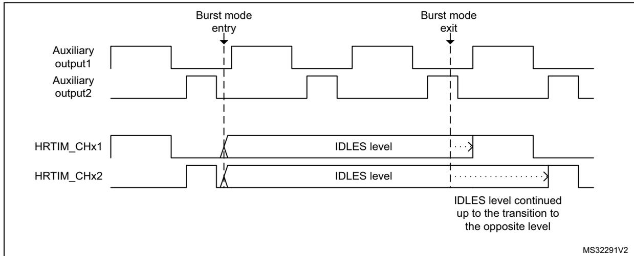
The signal on the auxiliary output can be slightly distorted when exiting from the burst mode or when re-enabling the outputs after a delayed protection, if this happens during a deadtime. In this case, the deadtime applied to the auxiliary outputs is extended so that the deadtime on the main outputs is respected. Figure 276 gives some examples.
Figure 276. Deadtime distortion on auxiliary output when exiting burst mode
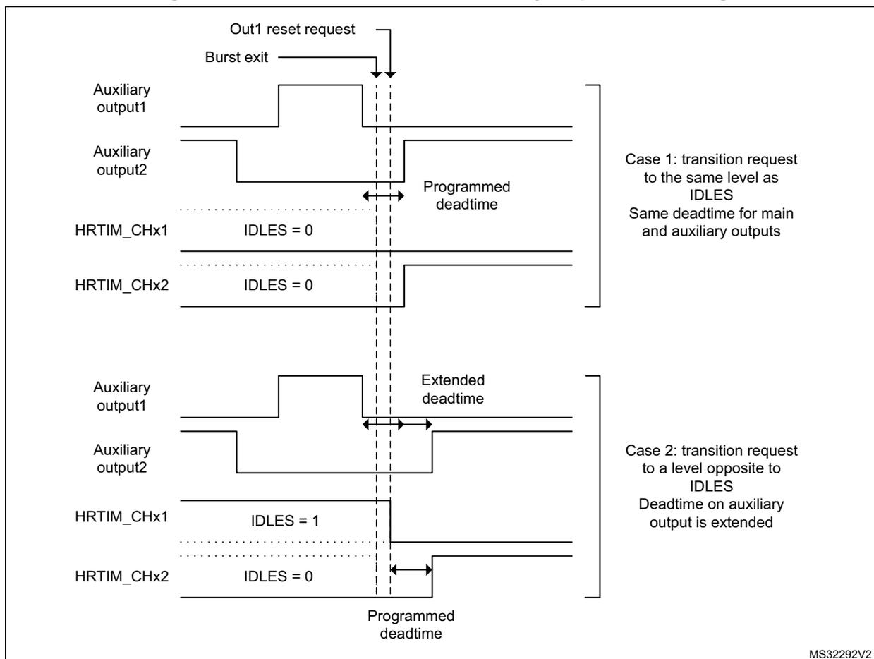
Out1 reset request
Burst exit
Auxiliary output1
Auxiliary output2
Programmed deadtime
HRTIM_CHx1 IDLES = 0
HRTIM_CHx2 IDLES = 0
Case 1: transition request to the same level as IDLES
Same deadtime for main and auxiliary outputs
Auxiliary output1
Auxiliary output2
Extended deadtime
HRTIM_CHx1 IDLES = 1
HRTIM_CHx2 IDLES = 0
Programmed deadtime
Case 2: transition request to a level opposite to IDLES
Deadtime on auxiliary output is extended
28.3.19 Synchronizing the HRTIM with other timers or HRTIM instances
The HRTIM provides options for synchronizing multiple HRTIM instances, as a master unit (generating a synchronization signal) or as a slave (waiting for a trigger to be synchronized). This feature can also be used to synchronize the HRTIM with other timers, either external or on-chip. The synchronization circuitry is controlled inside the master timer.
Synchronization output
This section explains how the HRTIM must be configured to synchronize external resources and act as a master unit.
Four events can be selected as the source to be sent to the synchronization output. This is done using SYNCSRC[1:0] bits in the HRTIM_MCR register, as follows:
- • 00: master timer start
This event is generated when MCEN bit is set or when the timer is re-started after having reached the period value in single-shot mode. It is also generated on a reset which occurs during the counting (when CONT or RETRIG bits are set). - • 01: master timer compare 1 event
- • 10: timer A start
This event is generated when TACEN bit is set or when the counter is reset and restarts counting in response to this reset. The following counter reset events are not propagated to the synchronization output: counter roll-over in continuous mode, and discarded reset request in single-shot non-retriggerable mode. The reset is only taken into account when it occurs during the counting (CONT or RETRIG bits are set). - • 11: timer A compare 1 event
SYNCOUT[1:0] bits in the HRTIM_MCR register specify how the synchronization event is generated.
The synchronization pulses can be generated on the HRTIM_SCOUT output pin, with SYNCSRC[1:0] = 1x. SYNCSRC[0] bit specifies the polarity of the synchronization signal. If SYNCSRC[0] = 0, the HRTIM_SCOUT pin has a low idle level and issues a positive pulse of 16 \( f_{HRTIM} \) clock cycles length for the synchronization). If SYNCSRC[0] = 1, the idle level is high and a negative pulse is generated.
Note: The synchronization pulse is followed by an idle level of 16 \( f_{HRTIM} \) clock cycles during which any new synchronization request is discarded. Consequently, the maximum synchronization frequency is \( f_{HRTIM}/32 \) .
The idle level on the HRTIM_SCOUT pin is applied as soon as the SYNCSRC[1:0] bits are enabled (i.e. the bitfield value is different from 00).
The synchronization output initialization procedure must be done prior to the configuration of the MCU outputs and counter enable, in the following order:
- 1. SYNCSRC[1:0] and SYNCSRC[1:0] bitfield configuration in HRTIM_MCR
- 2. HRTIM_SCOUT pin configuration (see the General-purpose I/Os section)
- 3. Master or timer A counter enable (MCEN or TACEN bit set)
When the synchronization input mode is enabled and starts the counter (using SYNCSTRTM/SYNCSTRTx bits) simultaneously with the synchronization output mode (SYNCSRC[1:0] = 00 or 10), the output pulse is generated only when the counter is starting or is reset while running. Any reset request clearing the counter without causing it to start does not affect the synchronization output.
Synchronization input
The HRTIM can be synchronized by external sources, as per the programming of the SYNCIN[1:0] bits in the HRTIM_MCR register:
- • 00: synchronization input is disabled
- • 01: reserved configuration
- • 10: the On-chip timer TRGO output connected to hrtim_in_sync[2] input (refer to Table 222 for details).
- • 11: a positive pulse on the HRTIM_SCIN input pin (hrtim_in_sync[3])
This bitfield cannot be changed once the destination timer (master timer or timing unit) is enabled (MCEN and/or TxCEN bit set).
The HRTIM_SCIN input is rising-edge sensitive. The timer behavior is defined with the following bits present in HRTIM_MCR and HRTIM_TIMxCR registers (see Table 254 for details):
- • Synchronous start: the incoming signal starts the timer's counter (SYNCSTRM and/or SYNCSTRTx bits set). TxCEN (MCEN) bits must be set to have the timer enabled and the counter ready to start. In continuous mode, the counter does not start until the synchronization signal is received.
- • Synchronous reset: the incoming signal resets the counter (SYNCRSTM and/or SYNCRSTx bits set). This event decrements the repetition counter as any other reset event.
The synchronization events are taken into account only once the related counters are enabled (MCEN or TxCEN bit set). A synchronization request triggers a SYNC interrupt.
Note: A synchronized start event resets the counter if the current counter value is above the active period value.
The effect of the synchronization event depends on the timer operating mode, as summarized in Table 254 .
Table 254. Effect of sync event versus timer operating modes
| Operating mode | SYNC RSTx | SYNC STRTx | Behavior following a SYNC reset or start event |
|---|---|---|---|
| Single-shot non-retriggerable | 0 | 1 | Start events are taken into account when the counter is stopped and: – once the MCEN or TxCEN bits are set – once the period has been reached. A start occurring when the counter is stopped at the period value resets the counter. A reset request clears the counter but does not start it (the counter can solely be re-started with the synchronization). Any reset occurring during the counting is ignored (as during regular non-retriggerable mode). |
| 1 | X | Reset events are starting the timer counting. They are taken into account only if the counter is stopped and: – once the MCEN or TxCEN bits are set – once the period has been reached. When multiple reset requests are selected (from HRTIM_SCIN and from internal events), only the first arriving request is taken into account. |
Table 254. Effect of sync event versus timer operating modes (continued)
| Operating mode | SYNC RSTx | SYNC STRTx | Behavior following a SYNC reset or start event |
|---|---|---|---|
| Single-shot retriggerable | 0 | 1 | The counter start is effective only if the counter is not started or period is elapsed. Any synchronization event occurring after counter start has no effect. A start occurring when the counter is stopped at the period value resets the counter. A reset request clears the counter but does not start it (the counter can solely be started by the synchronization). A reset occurring during counting is taken into account (as during regular retriggerable mode). |
| 1 | X | The reset from HRTIM_SCIN is taken into account as any HRTIM's timer counter reset from internal events and is starting or re-starting the timer counting. When multiple reset requests are selected, the first arriving request is taken into account. | |
| Continuous mode | 0 | 1 | The timer is enabled (MCEN or TxCEN bit set) and is waiting for the synchronization event to start the counter. Any synchronization event occurring after the counter start has no effect (the counter can solely be started by the synchronization). A reset request clears the counter but does not start it. |
| 1 | X | The reset from HRTIM_SCIN is taken into account as any HRTIM's timer counter reset from internal events and is starting or re-starting the timer counting. When multiple reset requests are selected, the first arriving request is taken into account. |
When a synchronization reset event occurs within the same \( f_{HRTIM} \) clock cycle as the period event, this reset is postponed to a programmed period event (since both events are causing a counter roll-over). This applies only when the high-resolution is active (CKPSC[2:0] < 5).
Figure 277 presents how the synchronized start is done in single-shot mode.
Figure 277. Counter behavior in synchronized start mode
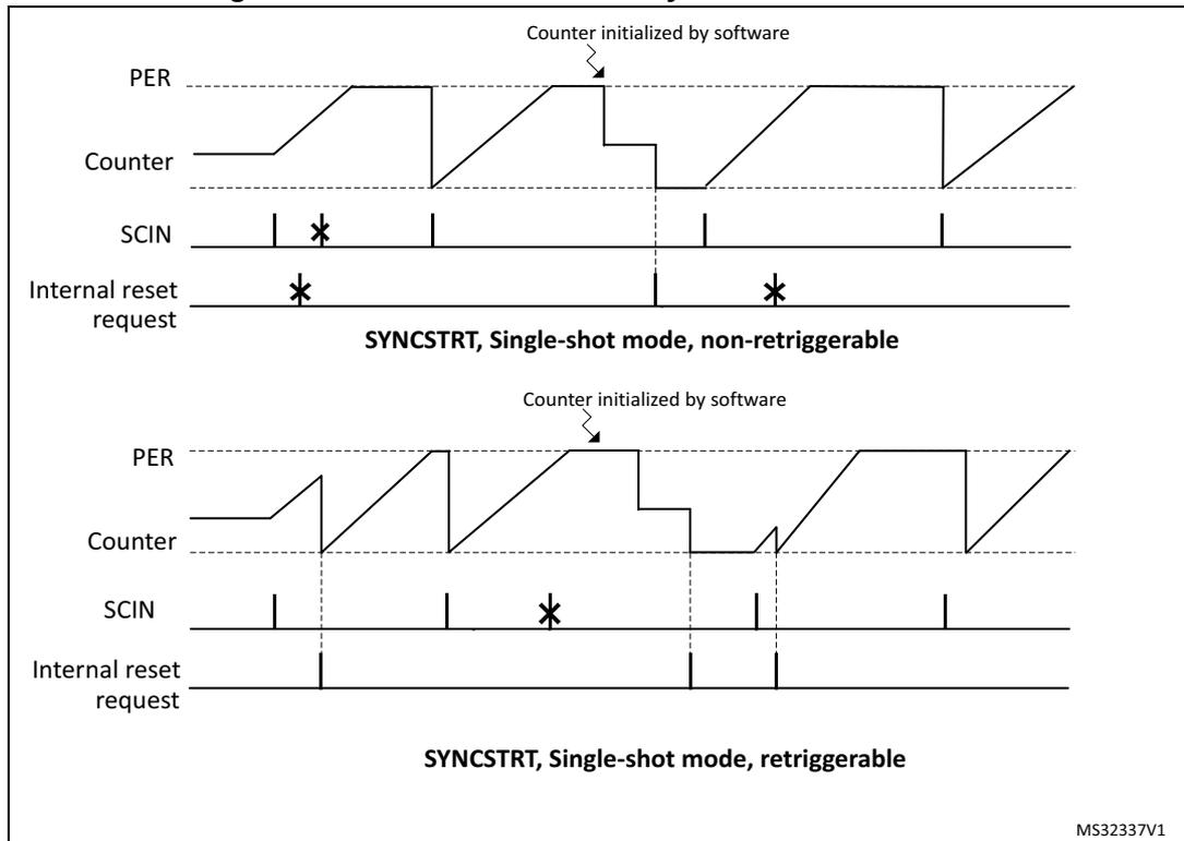
SYNCSTRT, Single-shot mode, non-retriggerable
SYNCSTRT, Single-shot mode, retriggerable
MS32337V1
28.3.20 ADC triggers
The ADCs can be triggered by the master and the 6 timing units.
10 independent triggers are available for both the regular and the injected sequencers of the ADCs. The external events can be used as triggers. They are taken right after the conditioning defined in the HRTIM_EECRx registers, and are not depending on the EEFxR1 and EEFxR2 register settings.
Up to 32 events can be combined (ORed) for ADC triggers 1 to 4, in HRTIM_ADC1R to HRTIM_ADC4R registers, as shown on Figure 278. The ADC triggers 1/3 and 2/4 are using the same source set. A multiple triggering is possible within a single switching period by selecting several sources simultaneously. A typical use case is for a non-overlapping multiphase converter, where all phases can be sampled in a row using a single ADC trigger output.
Figure 278. ADC trigger selection overview
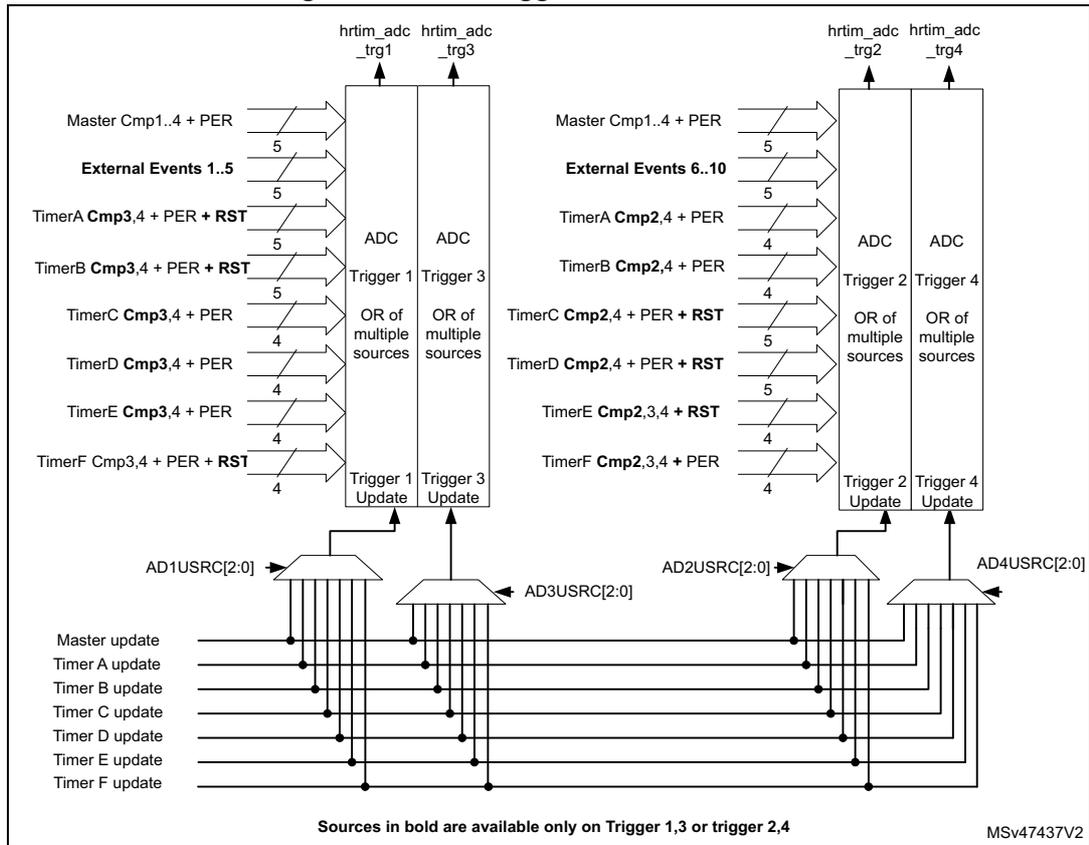
The diagram illustrates the ADC trigger selection for the HRTIM. It is divided into two main sections for ADC 1 and ADC 2.
- ADC 1:
- Trigger 1: Sources include Master Cmp1..4 + PER, External Events 1..5, TimerA Cmp3,4 + PER + RST, TimerB Cmp3,4 + PER + RST, TimerC Cmp3,4 + PER, TimerD Cmp3,4 + PER, TimerE Cmp3,4 + PER, and TimerF Cmp3,4 + PER + RST. It is controlled by AD1USRC[2:0].
- Trigger 3: Sources include Master Cmp1..4 + PER, External Events 1..5, TimerA Cmp3,4 + PER + RST, TimerB Cmp3,4 + PER + RST, TimerC Cmp3,4 + PER, TimerD Cmp3,4 + PER, TimerE Cmp3,4 + PER, and TimerF Cmp3,4 + PER + RST. It is controlled by AD3USRC[2:0].
- ADC 2:
- Trigger 2: Sources include Master Cmp1..4 + PER, External Events 6..10, TimerA Cmp2,4 + PER, TimerB Cmp2,4 + PER, TimerC Cmp2,4 + PER + RST, TimerD Cmp2,4 + PER + RST, TimerE Cmp2,3,4 + RST, and TimerF Cmp2,3,4 + PER. It is controlled by AD2USRC[2:0].
- Trigger 4: Sources include Master Cmp1..4 + PER, External Events 6..10, TimerA Cmp2,4 + PER, TimerB Cmp2,4 + PER, TimerC Cmp2,4 + PER + RST, TimerD Cmp2,4 + PER + RST, TimerE Cmp2,3,4 + RST, and TimerF Cmp2,3,4 + PER. It is controlled by AD4USRC[2:0].
Common source lines for all triggers include Master update, Timer A update, Timer B update, Timer C update, Timer D update, Timer E update, and Timer F update. A note indicates that sources in bold are available only on Trigger 1, 3 or trigger 2, 4.
The ADC triggers 5 to 10 are configured in the HRTIM_ADCER register, as shown on Figure 279. The ADC triggers 5/7/9 and 6/8/10 are using the same source set.
A single source can be selected at once for these triggers (1 out of 32 possible events).
Figure 279. ADC triggers
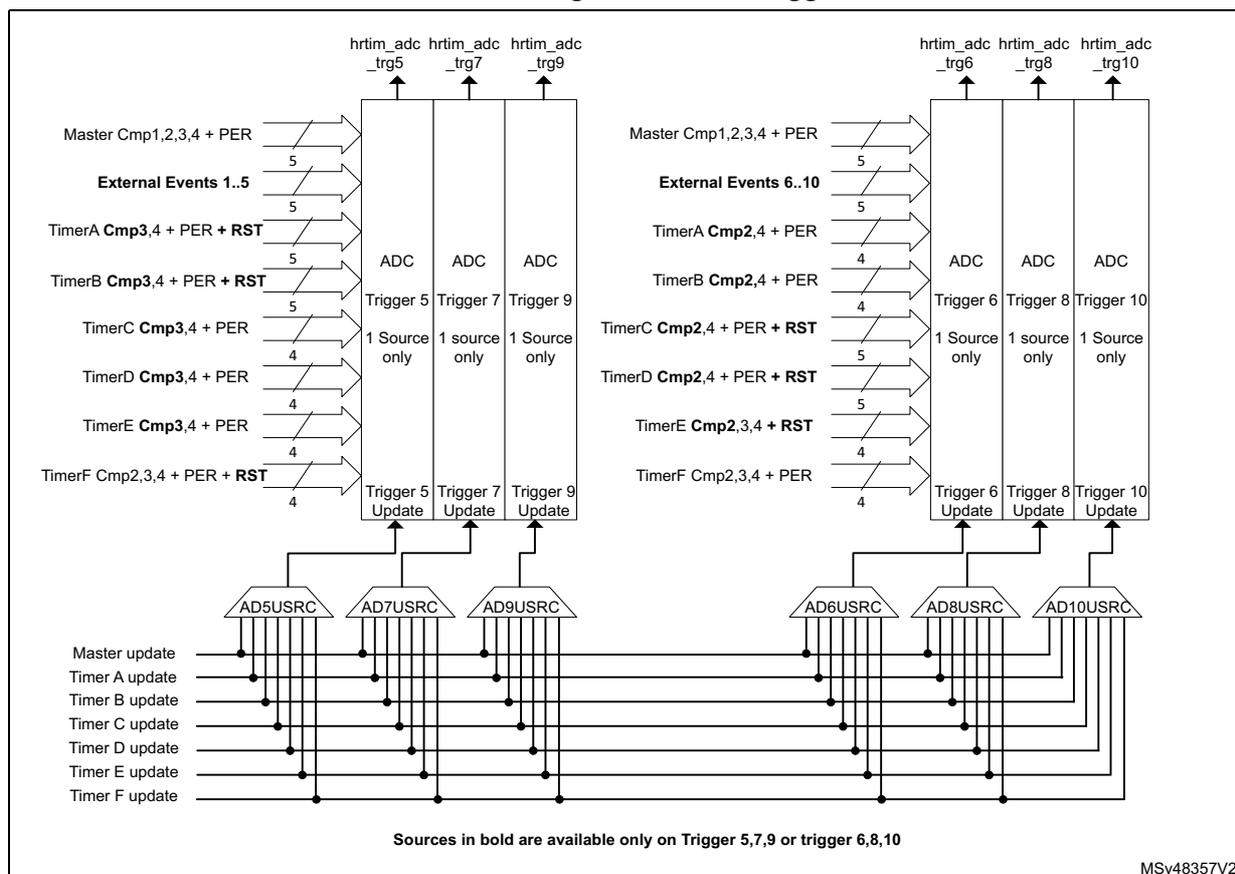
Sources in bold are available only on Trigger 5,7,9 or trigger 6,8,10
MSv48357V2
HRTIM_ADC1R to HRTIM_ADC4R and HRTIM_ADCER registers are preloaded and can be updated synchronously with the timer they are related to. The update sources are defined with ADxUSRC[2:0] bits in the HRTIM_CR1 and HRTIM_ADCUR registers.
For instance, if ADC trigger 1 outputs timer A CMP2 events (HRTIM_ADC1R = 0x0000 0400), HRTIM_ADC1R is typically updated simultaneously with timer A (AD1USRC[2:0] = 001).
When the preload is disabled (PREEN bit reset) in the source timer, the HRTIM_ADCxR registers are not preloaded either: a write access results in an immediate update of the trigger source.
ADC post-scaler
A post-scaling unit allows to reduce the ADC trigger rate with respect to the switching frequency.
Each ADC trigger rate can be individually adjusted using the ADCxPSC[4:0] bits in the HRTIM_ADCxPS1 and HRTIM_ADCxPS2 registers as shown in Figure 280 below for the up-counting mode.
In the center-aligned mode, the ADC post-scaling is done on events selected with the ADROM[1:0] bitfield, programmed in the source timer, as shown in Figure 281. The
ADROM[1:0] bitfield is coding for any event that can trigger the ADC: reset, roll-over (period) and compare event:
- • ADROM[1:0] = 00: event generated both during up and down-counting phases
- • ADROM[1:0] = 01: event generated during down-counting phases
- • ADROM[1:0] = 10: event generated during up-counting phases
The ADC post-scaler programming register are preloaded and can be updated on-the-fly without stopping the timers.
Figure 280. ADC trigger post-scaling in up-counting mode
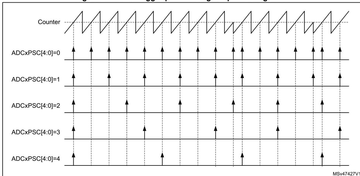
This diagram shows a sawtooth counter waveform at the top. Below it are five rows of trigger pulses corresponding to different post-scaler settings:
- Counter : A sawtooth wave representing the timer value.
- ADCxPSC[4:0]=0 : A trigger pulse occurs at every counter reset (period end).
- ADCxPSC[4:0]=1 : A trigger pulse occurs every 2nd counter reset.
- ADCxPSC[4:0]=2 : A trigger pulse occurs every 3rd counter reset.
- ADCxPSC[4:0]=3 : A trigger pulse occurs every 4th counter reset.
- ADCxPSC[4:0]=4 : A trigger pulse occurs every 5th counter reset.
MSv47427V1
Figure 281. ADC trigger post-scaling in up/down counting mode
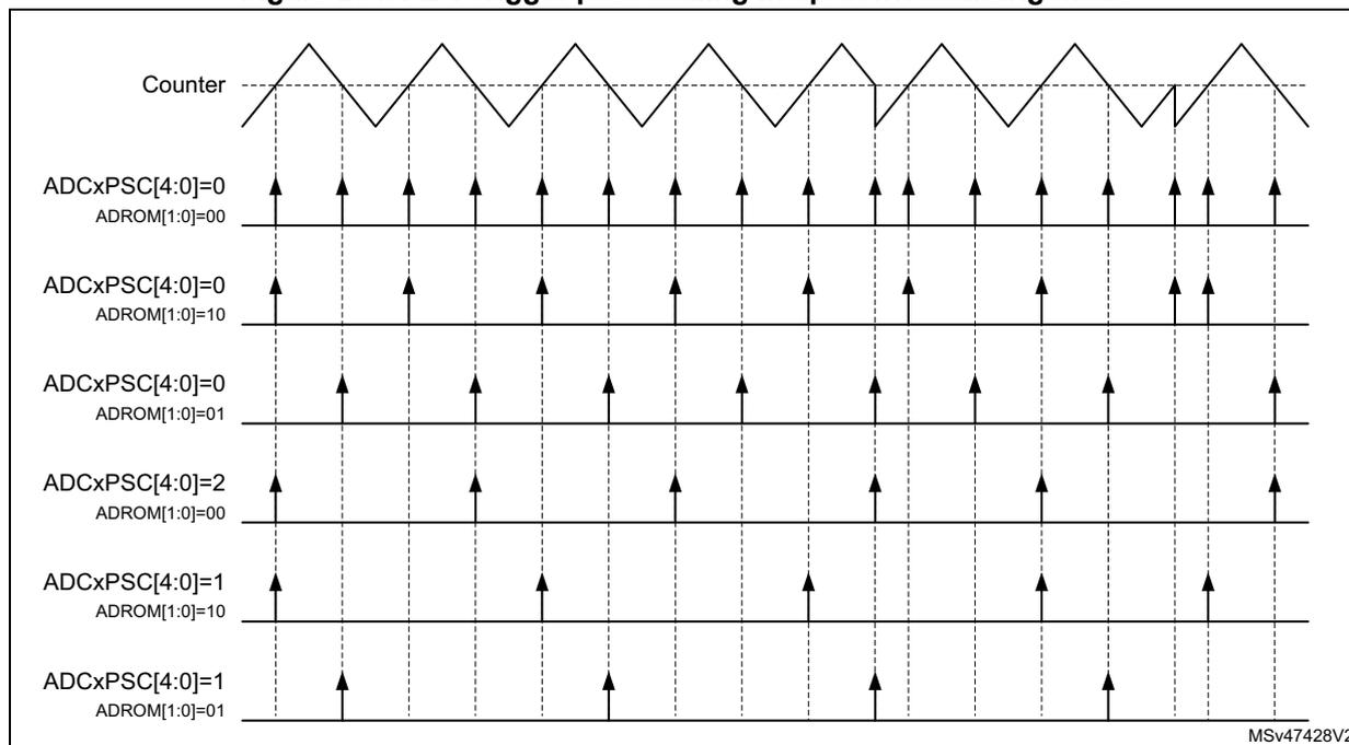
This diagram shows a triangular counter waveform (up/down counting). Below it are six rows of trigger pulses based on post-scaler (ADCxPSC) and direction selection (ADROM):
- Counter : A triangular wave.
- ADCxPSC[4:0]=0, ADROM[1:0]=00 : Triggers at every peak and every valley.
- ADCxPSC[4:0]=0, ADROM[1:0]=10 : Triggers only at peaks (end of up-counting).
- ADCxPSC[4:0]=0, ADROM[1:0]=01 : Triggers only at valleys (end of down-counting).
- ADCxPSC[4:0]=2, ADROM[1:0]=00 : Triggers at every 3rd event (alternating peaks and valleys).
- ADCxPSC[4:0]=1, ADROM[1:0]=10 : Triggers at every 2nd peak.
- ADCxPSC[4:0]=1, ADROM[1:0]=01 : Triggers at every 2nd valley.
MSv47428V2
28.3.21 DAC triggers
The HRTIM allows to have the embedded DACs updated synchronously with the timer updates.
The update events from the master timer and the timer units can generate DAC update triggers on any of the 3 hrtim_dac_trgx outputs.
Note: Each timer has its own DAC-related control register.
DACSYNC[1:0] bits of the HRTIM_MCR and HRTIM_TIMxCR registers are programmed as follows:
- • 00: No update generated
- • 01: Update generated on hrtim_dac_trg1
- • 10: Update generated on hrtim_dac_trg2
- • 11: Update generated on hrtim_dac_trg3
An output pulse of 1 \( f_{HRTIM} \) clock periods is generated on the hrtim_dac_trgx output.
When DACSYNC[1:0] bits are enabled in multiple timers, the hrtim_dac_trgx output consists of an OR of all timers' update events. For instance, if DACSYNC = 1 in timer A and in timer B, the update event in timer A is ORed with the update event in timer B to generate a DAC update trigger on the corresponding hrtim_dac_trgx output, as shown on Figure 282.
Figure 282. Combining several updates on a single hrtim_dac_trgx output
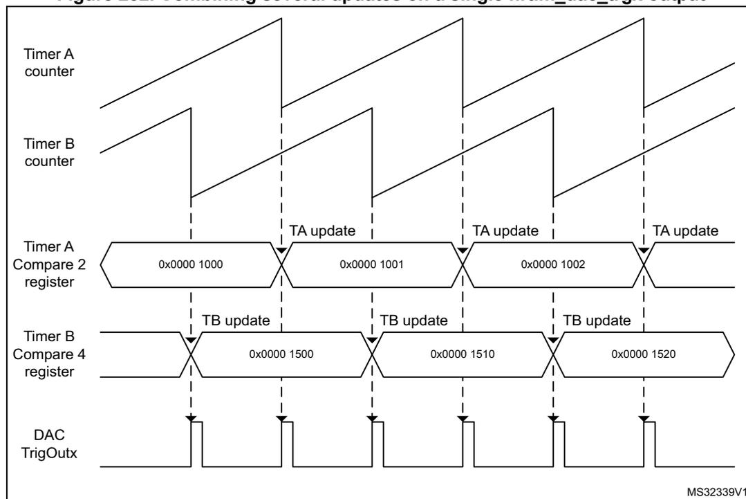
The diagram illustrates the timing relationship between two timers, Timer A and Timer B, and their associated DAC trigger output. The top two waveforms represent the counters for Timer A and Timer B, both showing a sawtooth pattern. Below these, the 'Timer A Compare 2 register' shows a sequence of values: 0x0000 1000, 0x0000 1001, and 0x0000 1002. The 'Timer B Compare 4 register' shows a sequence of values: 0x0000 1500, 0x0000 1510, and 0x0000 1520. Vertical dashed lines indicate update events for both timers. The 'DAC TrigOutx' output at the bottom shows a series of pulses. Each pulse is generated when either a 'TA update' (from Timer A) or a 'TB update' (from Timer B) occurs, demonstrating that the output is the logical OR of both timer update events. The diagram is labeled with 'MS32339V1' in the bottom right corner.
Refer to Table 229: HRTIM DAC triggers connections for connections to the DACs.
Dual channel DAC trigger
Slope compensation techniques and hysteretic control to be easily implemented using HRTIM built-in features and the DAC sawtooth generator. The principle is to have a DAC generating a decreasing saw-tooth synchronized with the PWM period, or a square wave synchronized with PWM signal.
This mode is enabled with the DCDE bit in the TIMxCR2 register. This bit cannot be changed once the timer is operating (TxEN bit set).
It uses two trigger outputs, as shown on the Figure 283 below:
- - the hrtim_dac_reset_trgx generates DAC reset/update events
- - the hrtim_dac_step_trgx generates requests for incremental DAC value changes
The DCDR bit in the TIMxCR2 register defines when the hrtim_dac_reset_trgx trigger is generated:
- • DCDR = 0: the trigger is generated on counter reset or roll-over event
- • DCDR = 1: the trigger is generated on output 1 set event
Note: The DCDR bit is not significant when the DCDE bit is reset (Dual channel DAC trigger disabled).
The DCDS bit in the TIMxCR2 register defines when the hrtim_dac_step_trgx trigger is generated:
- • DCDS = 0: the trigger is generated on compare 2 event
- • DCDS = 1: the trigger is generated on output 1 reset event
The DCDR and DCDS bits allows the following use cases to be covered:
- – Edge-aligned slope compensation (DCDR = DCDS = 0): the DAC's sawtooth starts on PWM period beginning and multiple triggers are generated during the period
- – Center-aligned slope compensation (DCDR = 1 DCDS = 0): the DAC's sawtooth starts on the output set event and multiple triggers are generated during the period
- – Hysteretic controller: the DAC value must be changed twice per period, when the output state changes. 2 triggers are generated per PWM period. In edge-aligned mode (DCDR=0, DCDS =1), the triggers are generated on counter reset or roll-over. In center-aligned mode (DCDR=1, DCDS=1), the triggers are generated when the output is set.
The compare 2 has a particular operating mode when the DCDE is set and the DCDS bit is reset. The active comparison value is automatically updated as soon as a compare match has occurred, so that the trigger can be repeated periodically with a period equal to the CMP2 value, as represented on Figure 283 .
The dual channel DAC trigger with DCDS bit reset (compare 2 event used) must not be used simultaneously with modes using CMP2 (triple / quad interleaved and triggered-half modes).
Note: The CMP2 value can be changed on-the-fly. The new value is taken into account on the next coming compare match.
Note: When the DCDS bit is reset, the CMP2 value must not be modified by other mechanisms: the interleaved, triggered half and balanced idle modes must be disabled.
Table 255 below gives an example, for generating 6 triggers within a PWM period. It shows that it is necessary to round up the division result to the upper value.
Let's consider a counter period TIMxPER = 8192. Dividing 8192 by 6 yields 1365.33.
- – Round down value: 1365: 7 triggers are generated, the 6th and 7th being very close (respectively for counter = 8190 and 8192)
- – Round up value: 1366: 6 triggers are generated. The 6th trigger on dac_step_trg (for counter = 8192) is aborted by the counter roll-over from 8192 to 0.
Table 255. DAC dual channel trigger example
| - | CMP2 = 1365 | dac_trg | dac_step_trg | CMP2 = 1366 | dac_trg | dac_step_trg |
|---|---|---|---|---|---|---|
| Counter value | 1365 | - | 1 | 1366 | - | 1 |
| 2730 | - | 2 | 2732 | - | 2 | |
| 4095 | - | 3 | 4098 | - | 3 | |
| 5460 | - | 4 | 5464 | - | 4 | |
| 6825 | - | 5 | 6830 | - | 5 | |
| 8190 | - | 6 | 8192 | 6 | - | |
| 8192 | 7 | - | 1366 | - | 1 | |
| 1365 | - | 1 | 2732 | - | 2 | |
| ... | - | - | ... | - | - |
Note: In centered-pattern mode, it is mandatory to have an even number of triggers per switching period, so as to avoid unevenly spaced triggers around counter's peak value.
Figure 283. DAC triggers for slope compensation
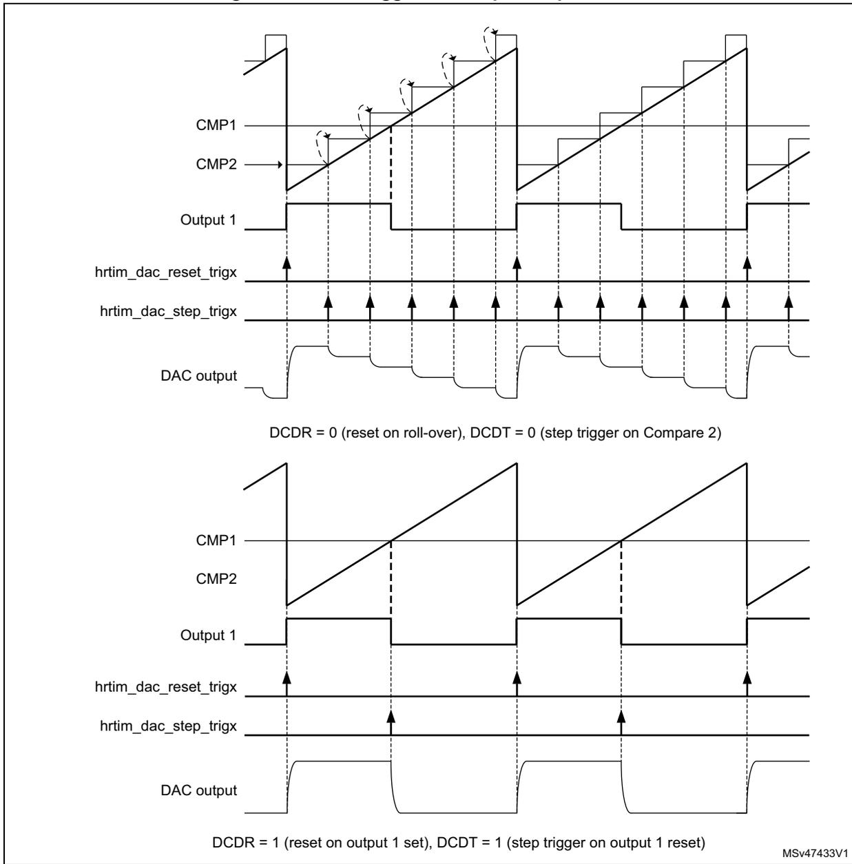
The figure consists of two timing diagrams illustrating the relationship between HRTIM signals and a DAC output for slope compensation.
Top Diagram: This diagram shows the timing when DCDR = 0 (reset on roll-over) and DCDT = 0 (step trigger on Compare 2). The waveforms are:
- CMP1 and CMP2 : Comparison signals. CMP1 is a constant high level. CMP2 is a sawtooth-like signal that ramps up and is reset by the roll-over event.
- Output 1 : A PWM signal that is high when the counter is below the compare value of CMP1 and low otherwise.
- hrtim_dac_reset_trigx : A pulse that goes high at the roll-over event (when the counter reaches its maximum value).
- hrtim_dac_step_trigx : A pulse that goes high whenever CMP2 crosses the CMP1 level.
- DAC output : A staircase-like signal that is reset to a minimum value at the roll-over event and then incremented by one step at each rising edge of hrtim_dac_step_trigx.
Bottom Diagram: This diagram shows the timing when DCDR = 1 (reset on output 1 set) and DCDT = 1 (step trigger on output 1 reset). The waveforms are:
- CMP1 and CMP2 : Similar to the top diagram, but the sawtooth signal in CMP2 is reset when Output 1 goes high.
- Output 1 : The same PWM signal as above.
- hrtim_dac_reset_trigx : A pulse that goes high when Output 1 goes high (at the start of each PWM period).
- hrtim_dac_step_trigx : A pulse that goes high when Output 1 goes low (at the end of each PWM period).
- DAC output : A staircase-like signal that is reset to a minimum value when Output 1 goes high and then incremented by one step when Output 1 goes low.
MSV47433V1
The Figure 284 below provides an overview of all the available DAC triggers.
Figure 284. DAC triggers overview
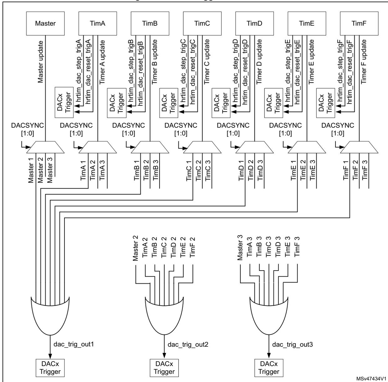
The diagram illustrates the DAC trigger hierarchy. At the top, seven timer blocks are shown: Master, TimA, TimB, TimC, TimD, TimE, and TimF. Each timer has associated trigger signals:
- Master: Master update, DACSYNC [1:0].
- TimA: hrtim_dac_step_trigA, hrtim_dac_reset_trigA, Timer A update, DACx Trigger, DACSYNC [1:0].
- TimB: hrtim_dac_step_trigB, hrtim_dac_reset_trigB, Timer B update, DACx Trigger, DACSYNC [1:0].
- TimC: hrtim_dac_step_trigC, hrtim_dac_reset_trigC, Timer C update, DACx Trigger, DACSYNC [1:0].
- TimD: hrtim_dac_step_trigD, hrtim_dac_reset_trigD, Timer D update, DACx Trigger, DACSYNC [1:0].
- TimE: hrtim_dac_step_trigE, hrtim_dac_reset_trigE, Timer E update, DACx Trigger, DACSYNC [1:0].
- TimF: hrtim_dac_step_trigF, hrtim_dac_reset_trigF, Timer F update, DACx Trigger, DACSYNC [1:0].
- dac_trig_out1 is the OR of Master 1, Master 2, and Master 3.
- dac_trig_out2 is the OR of Master 2, TimA 2, TimB 2, TimC 2, TimD 2, TimE 2, and TimF 2.
- dac_trig_out3 is the OR of Master 3, TimA 3, TimB 3, TimC 3, TimD 3, TimE 3, and TimF 3.
28.3.22 Interrupts
7 interrupts can be generated by the master timer:
- • Master timer registers update
- • Synchronization event received
- • Master timer repetition event
- • Master compare 1 to 4 event
14 interrupts can be generated by each timing unit:
- • Delayed protection triggered
- • Counter reset or roll-over event
- • Output 1 and output 2 reset (transition active to inactive)
- • Output 1 and output 2 set (transition inactive to active)
- • Capture 1 and 2 events
- • Timing unit registers update
- • Repetition event
- • Compare 1 to 4 event
8 global interrupts are generated for the whole HRTIM:
- • System fault and fault 1 to 6 (regardless of the timing unit attribution)
- • DLL calibration done
- • Burst mode period completed
The interrupt requests are grouped in 8 vectors as follows:
- • hrtim_it1: master timer interrupts (master update, sync Input, repetition, MCMP1..4) and global interrupt except faults (burst mode period and DLL ready interrupts)
- • hrtim_it2: TIMA interrupts
- • hrtim_it3: TIMB interrupts
- • hrtim_it4: TIMC interrupts
- • hrtim_it5: TIMD interrupts
- • hrtim_it6: TIME interrupts
- • hrtim_it7: TIMF interrupts
- • hrtim_it8: Dedicated vector all fault interrupts to allow high-priority interrupt handling
Table 256 is a summary of the interrupt requests, their mapping and associated control, and status bits.
Table 256. HRTIM interrupt summary
| Interrupt vector | Interrupt event | Event flag | Enable control bit | Flag clearing bit |
|---|---|---|---|---|
| hrtim_it1 | Burst mode period completed | BMPER | BMPERIE | BMPERC |
| DLL calibration done | DLLRDY | DLLRDYIE | DLLRDYC | |
| Master timer registers update | MUPD | MUPDIE | MUPDC | |
| Synchronization event received | SYNC | SYNCIE | SYNCC | |
| Master timer repetition event | MREP | MREPIE | MREPC | |
| Master compare 1 to 4 event | MCMP1 | MCMP1IE | MCP1C | |
| MCMP2 | MCMP2IE | MCP2C | ||
| MCMP3 | MCMP3IE | MCP3C | ||
| MCMP4 | MCMP4IE | MCP4C |
Table 256. HRTIM interrupt summary (continued)
| Interrupt vector | Interrupt event | Event flag | Enable control bit | Flag clearing bit |
|---|---|---|---|---|
| hrtim_it2 hrtim_it3 hrtim_it4 hrtim_it5 hrtim_it6 hrtim_it7 | Delayed protection triggered | DLYPRT | DLYPRTIE | DLYPRTC |
| Counter reset or roll-over event | RST | RSTIE | RSTC | |
| Output 1 and output 2 reset (transition active to inactive) | RSTx1 | RSTx1IE | RSTx1C | |
| RSTx2 | RSTx2IE | RSTx2C | ||
| Output 1 and output 2 set (transition inactive to active) | SETx1 | SETx1IE | SETx1C | |
| SETx2 | SETx2IE | SETx2C | ||
| Capture 1 and 2 events | CPT1 | CPT1IE | CPT1C | |
| CPT2 | CPT2IE | CPT2C | ||
| Timing unit registers update | UPD | UPDIE | UPDC | |
| Repetition event | REP | REPIE | REPC | |
| hrtim_it8 | Compare 1 to 4 event | CMP1 | CMP1IE | CMP1C |
| CMP2 | CMP2IE | CMP2C | ||
| CMP3 | CMP3IE | CMP3C | ||
| CMP4 | CMP4IE | CMP4C | ||
| System fault | SYSFLT | SYSFLTIE | SYSFLTC | |
| Fault 1 to 6 | FLT1 | FLT1IE | FLT1C | |
| FLT2 | FLT2IE | FLT2C | ||
| FLT3 | FLT3IE | FLT3C | ||
| FLT4 | FLT4IE | FLT4C | ||
| FLT5 | FLT5IE | FLT5C | ||
| FLT6 | FLT6IE | FLT6C |
28.3.23 DMA
Most of the events able to generate an interrupt can also generate a DMA request, even both simultaneously. Each timer (master, TIMA...F) has its own DMA enable register.
The individual DMA requests are ORed into 7 channels as follows:
- • 1 channel for the master timer
- • 1 channel per timing unit (TIMA...F)
Note: Before disabling a DMA channel (DMA enable bit reset in TIMxDIER), it is necessary to disable first the DMA controller.
Table 257 is a summary of the events with their associated DMA enable bits.
Table 257. HRTIM DMA request summary
| DMA Channel | Event | DMA capable | DMA enable bit |
|---|---|---|---|
| hrtim_dma1 (master timer) | Burst mode period completed | No | N/A |
| DLL calibration done | No | N/A | |
| Master timer registers update | Yes | MUPDDE | |
| Synchronization event received | Yes | SYNCDE | |
| Master timer repetition event | Yes | MREPDE | |
| Master compare 1 to 4 event | Yes | MCMP1DE | |
| Yes | MCMP2DE | ||
| Yes | MCMP3DE | ||
| Yes | MCMP4DE | ||
| hrtim_dma2 (timer A) hrtim_dma3 (timer B) hrtim_dma4 (timer C) hrtim_dma5 (timer D) hrtim_dma6 (timer E) hrtim_dma7 (timer F) | Delayed protection triggered | Yes | DLYPRTDE |
| Counter reset or roll-over event | Yes | RSTDE | |
| Output 1 and output 2 reset (transition active to inactive) | Yes | RSTx1DE | |
| Yes | RSTx2DE | ||
| Output 1 and output 2 set (transition inactive to active) | Yes | SETx1DE | |
| Yes | SETx2DE | ||
| Capture 1 and 2 events | Yes | CPT1DE | |
| Yes | CPT2DE | ||
| Timing unit registers update | Yes | UPDDE | |
| Repetition event | Yes | REPDE | |
| Compare 1 to 4 event | Yes | CMP1DE | |
| Yes | CMP2DE | ||
| Yes | CMP3DE | ||
| Yes | CMP4DE | ||
| N/A | System fault | No | N/A |
| Fault 1 to 6 | No | N/A | |
| Burst mode period completed | No | N/A | |
| DLL calibration done | No | N/A |
Burst DMA transfers
In addition to the standard DMA requests, the HRTIM features a DMA burst controller to have multiple registers updated with a single DMA request. This allows to:
- • update multiple data registers with one DMA channel only,
- • reprogram dynamically one or several timing units, for converters using multiple timer outputs.
The burst DMA feature is only available for one DMA channel, but any of the 6 channels can be selected for burst DMA transfers.
The principle is to program which registers are to be written by DMA. The master timer and TIMA..E have the burst DMA update register, where most of their control and data registers are associated with a selection bit: HRTIM_BDMUPR, HRTIM_BDTAUPR to HRTIM_BDTEUPR (this is applicable only for registers with write accesses). A redirection mechanism allows to forward the DMA write accesses to the HRTIM registers automatically, as shown on Figure 285.
Figure 285. DMA burst overview
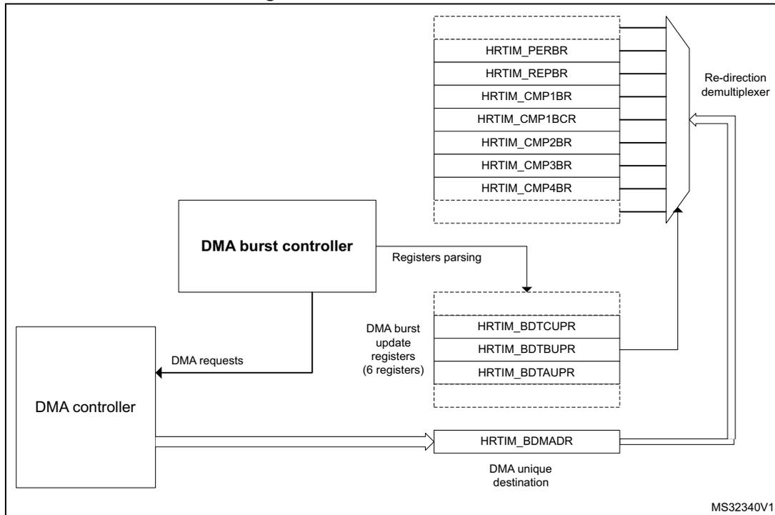
The diagram illustrates the DMA burst overview. On the left, a 'DMA controller' block is connected to a 'DMA burst controller' block via 'DMA requests'. The 'DMA burst controller' block is connected to a 'Registers parsing' block, which in turn is connected to a group of 'DMA burst update registers (6 registers)'. These registers are HRTIM_BDTUPR, HRTIM_BDTBUPR, and HRTIM_BDTAUPR. The 'Registers parsing' block is also connected to a 'Re-direction demultiplexer' block. The 'Re-direction demultiplexer' block is connected to a group of HRTIM registers: HRTIM_PERBR, HRTIM_REPBR, HRTIM_CMP1BR, HRTIM_CMP1BCR, HRTIM_CMP2BR, HRTIM_CMP3BR, and HRTIM_CMP4BR. The 'DMA burst controller' block is also connected to the HRTIM_BDMADR register, which is labeled 'DMA unique destination'. The HRTIM_BDMADR register is connected to the 'Re-direction demultiplexer' block. The diagram is labeled MS32340V1.
When the DMA trigger occurs, the HRTIM generates multiple 32-bit DMA requests and parses the update register. If the control bit is set, the write access is redirected to the associated register. If the bit is reset, the register update is skipped and the register parsing is resumed until a new bit set is detected, to trigger a new request. Once the 6 update registers (HRTIM_BDMUPR, 5x HRTIM_BDTxUPR) are parsed, the burst is completed and the system is ready for another DMA trigger (see the flowchart on Figure 286).
Note: Any trigger occurring while the burst is on-going is discarded, except if it occurs during the very last data transfer.
The burst DMA mode is permanently enabled (there is no enable bit). A burst DMA operation is started by the first write access into the HRTIM_BDMADR register.
It is only necessary to have the DMA controller pointing to the HRTIM_BDMADR register as the destination, in the memory, to the peripheral configuration with the peripheral increment mode disabled (the HRTIM handles internally the data re-routing to the final destination register).
To re-initialize the burst DMA mode if it was interrupted during a transaction, it is necessary to write at least to one of the 6 update registers.
Figure 286. Burst DMA operation flowchart
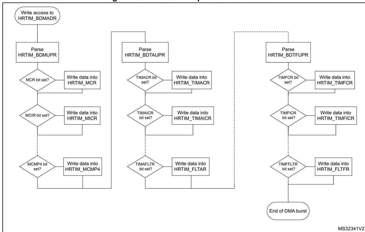
graph TD
    Start([Write access to HRTIM_BDMADR]) --> Parse1[Parse HRTIM_BDMUPR]
    Parse1 --> MCR{MCR bit set?}
    MCR -- Yes --> WriteMCR[Write data into HRTIM_MCR]
    WriteMCR --> MCIR{MCIR bit set?}
    MCIR -- Yes --> WriteMICR[Write data into HRTIM_MICR]
    WriteMICR --> MCMP4{MCMP4 bit set?}
    MCMP4 -- Yes --> WriteMCOMP4[Write data into HRTIM_MCOMP4]
    WriteMCOMP4 --> Parse2[Parse HRTIM_BDTAUPR]
    Parse2 --> TIMACR{TIMACR bit set?}
    TIMACR -- Yes --> WriteTIMACR[Write data into HRTIM_TIMACR]
    WriteTIMACR --> TIMAICR{TIMAICR bit set?}
    TIMAICR -- Yes --> WriteTIMAICR[Write data into HRTIM_TIMAICR]
    WriteTIMAICR --> TIMAFLTR{TIMAFLTR bit set?}
    TIMAFLTR -- Yes --> WriteFLTAR[Write data into HRTIM_FLTAR]
    WriteFLTAR --> Parse3[Parse HRTIM_BDTFUPR]
    Parse3 --> TIMFCR{TIMFCR bit set?}
    TIMFCR -- Yes --> WriteTIMFCR[Write data into HRTIM_TIMFCR]
    WriteTIMFCR --> TIMFICR{TIMFICR bit set?}
    TIMFICR -- Yes --> WriteTIMFICR[Write data into HRTIM_TIMFICR]
    WriteTIMFICR --> TIMFFLTR{TIMFFLTR bit set?}
    TIMFFLTR -- Yes --> WriteFLTFR[Write data into HRTIM_FLTFR]
    WriteFLTFR --> End([End of DMA burst])
MS32341V2
Several options are available once the DMA burst is completed, depending on the register update strategy.
If the PREEN bit is reset (preload disabled), the value written by the DMA is immediately transferred into the active register and the registers are updated sequentially, following the DMA transaction pace.
When the preload is enabled (PREEN bit set), there are 3 use cases:
- 1. The update is done independently from DMA burst transfers (UPDGAT[3:0] = 0000 in HRTIM_TIMxCR and BRSTDMA[1:0] = 00 in HRTIM_MCR). In this case, and if it is necessary to have all transferred data taken into account simultaneously, the user must check that the DMA burst is completed before the update event takes place. On the contrary, if the update event happens while the DMA transfer is on-going, only part of the registers is loaded and the complete register update requires 2 consecutive update events.
- 2. The update is done when the DMA burst transfer is completed (UPDGAT[3:0] = 0000 in HRTIM_TIMxCR and BRSTDMA[1:0] = 01 in HRTIM_MCR). This mode guarantees that all new register values are transferred simultaneously. This is done independently from the counter value and can be combined with regular update events, if necessary (for instance, an update on a counter reset when TxRSTU is set).
- 3. The update is done on the update event following the DMA burst transfer completion (UPDGAT[3:0] = 0010 in HRTIM_TIMxCR and BRSTDMA[1:0] = 10 in HRTIM_MCR). This mode guarantees both a coherent update of all transferred data and the synchronization with regular update events, with the timer counter. In this case, if a regular update request occurs while the transfer is on-going, it is discarded and the effective update happens on the next coming update request.
The chronogram on Figure 287 presents the active register content for 3 cases: PREEN=0, UPDGAT[3:0] = 0001 and UPDGAT[3:0] = 0001 (when PREEN = 1).
Figure 287. Registers update following DMA burst transfer
![Figure 287: Registers update following DMA burst transfer. This timing diagram illustrates the sequence of events during a DMA burst transfer to update HRTIM registers. It shows the Timer A Counter, DMA requests, DMA controller write accesses to BDMADR, and the resulting register content updates for two cases: PREEN=0 and PREEN=1. The diagram highlights the update of PER, CMP1, and CMP3 registers, showing 'previous' and 'new' values. Option 1 shows an update at the end of the DMA burst (UPDGAT[3:0] = 0001). Option 2 shows an update at the end of the DMA burst (UPDGAT[3:0] = 0010 and TxREPU = 1).](/RM0440-STM32G4/402bd0a5be217a0df3057b006469cc3c_img.jpg)
The diagram shows the following signal levels and events over time:
- Timer A Counter: A sawtooth waveform representing the counter value. A 'DMA request on CMP1 event starts DMA burst' occurs when the counter reaches the CMP1 threshold. A 'Repetition event' occurs when the counter reaches the PER threshold.
- DMA requests: A series of pulses generated by the timer when the counter matches the CMP1 or CMP3 thresholds.
- DMA controller write accesses to BDMADR: The controller writes to the BDMADR register to initiate a burst transfer. The sequence of writes is: PER, CMP1, CMP3.
- Register content PREEN=0:
- PER (previous) is updated to PER (new).
- CMP1 (previous) is updated to CMP1 (new).
- CMP3 (previous) is updated to CMP3 (new).
- Register content PREEN=1 (CMP3 showed only):
- CMP3 (previous) is updated to CMP3 (new) at two different possible points depending on the option.
- Option 1: update done at the end of the DMA burst transfer (UPDGAT[3:0] = 0001)
- Option 2: update done at the end of the DMA burst transfer (UPDGAT[3:0] = 0010 and TxREPU = 1)
MS32342V1
28.3.24 HRTIM initialization
This section describes the recommended HRTIM initialization procedure, including other related MCU peripherals.
The HRTIM clock source must be enabled in the reset and clock control unit (RCC), while respecting the \( f_{HRTIM} \) range for the DLL lock.
The DLL calibration must be started by setting CAL bit in HRTIM_DLLCR register.
The HRTIM master and timing units can be started only once the high-resolution unit is ready. This is indicated by the DLLRDY flag set. The DLLRDY flag can be polled before resuming the initialization or the calibration can run in background while other registers of the HRTIM or other MCU peripherals are initialized. In this case, the DLLRDY flag must be checked before starting the counters (an end-of-calibration interrupt can be issued if necessary, enabled with DLLRDYIE flag in HRTIM_IER). Once the DLL calibration is done, CALEN bit must be set to have it done periodically and compensate for potential voltage and temperature drifts. The calibration periodicity is defined using the CALRTE[1:0] bitfield in the HRTIM_DLLCR register.
The HRTIM control registers can be initialized as per the power converter topology and the timing units use case. All inputs have to be configured (source, polarity, edge-sensitivity).
The HRTIM outputs must be set up eventually, with the following sequence:
- • the polarity must be defined using POLx bits in HRTIM_OUTxR
- • the FAULT and IDLE states must be configured using FAULTx[1:0] and IDLESx bits in HRTIM_OUTxR
The HRTIM outputs are ready to be connected to the MCU I/Os. In the GPIO controller, the selected HRTIM I/Os have to be configured as per the alternate function mapping table in the product datasheet.
From this point on, the HRTIM controls the outputs, which are in the IDLE state.
The outputs are configured in RUN mode by setting TxyOEN bits in the HRTIM_OENR register. The 2 outputs are in the inactive state until the first valid set/reset event in RUN mode. Any output set/reset event (except software requests using SST, SRT) are ignored as long as TxCEN bit is reset, as well as burst mode requests (IDLEM bit value is ignored). Similarly, any counter reset request coming from the burst mode controller is ignored (if TxBM bit is set).
Note: When the deadtime insertion is enabled (DTEN bit set), it is necessary to force the output state by software, using SST and RST bits, to have the outputs in a complementary state as soon as the RUN mode is entered.
The HRTIM operation can eventually be started by setting TxCEN or MCEN bits in HRTIM_MCR.
If the HRTIM peripheral is reset with the Reset and Clock Controller, the output control is released to the GPIO controller and the outputs are tri stated.
28.3.25 Debug
When a microcontroller enters the debug mode (Cortex ® -M4 with FPU core halted), the TIMx counter either continues to work normally or stops, depending on DBG_HRTIM_STOP configuration bit in DBG module:
- • DBG_HRTIM_STOP = 0: no behavior change, the HRTIM continues to operate.
- • DBG_HRTIM_STOP = 1: all HRTIM timers, including the master, are stopped. The outputs in RUN mode enter the FAULT state if FAULTx[1:0] = 01,10,11, or keep their current state if FAULTx[1:0] = 00. The outputs in idle state are maintained in this state. This is permanently maintained even if the MCU exits the halt mode. This allows to maintain a safe state during the execution stopping. The outputs can be enabled again by settings TxyOEN bit (requires the use of the debugger).
Timer behavior during MCU halt when DBG_HRTIM_STOP = 1
The set/reset crossbar, the dead-time and push-pull unit, the idle/balanced fault detection and all the logic driving the normal output in RUN mode are not affected by debug. The output keeps on toggling internally, so as to retrieve regular signals of the outputs when TxyOEN is set again (during or after the MCU halt). Associated triggers and filters are also following internal waveforms when the outputs are disabled.
FAULT inputs and events (any source) are enabled during the MCU halt.
Fault status bits can be set and TxyOEN bits reset during the MCU halt if a fault occurs at that time (TxyOEN and TxyODS are not affected by DBG_HRTIM_STOP bit state).
Synchronization, counter reset, start and reset-start events are discarded in debug mode, as well as capture events. This is to keep all related registers stable as long as the MCU is halted.
The counter stops counting when a breakpoint is reached. However, the counter enable signal is not reset; consequently no start event is emitted when exiting from debug. All counter reset and capture triggers are disabled, as well as external events (ignored as long as the MCU is halted). The outputs SET and RST flags are frozen, except in case of forced software set/reset. A level-sensitive event is masked during the debug but is active again as soon as the debug is exited. For edge-sensitive events, if the signal is maintained active during the MCU halt, a new edge is not generated when exiting from debug.
The update events are discarded. This prevents any update trigger on hrtim_upd_en[3:1] inputs. DMA triggers are disabled. The burst mode circuit is frozen: the triggers are ignored and the burst mode counter stopped.
DLL calibration is not blocked while the MCU is halted (the DLLRDY flag can be set).
28.4 Application use cases
28.4.1 Buck converter
Buck converters are of common use as step-down converters. The HRTIM can control up to 12 buck converters with 7 independent switching frequencies.
The converter usually operates at a fixed frequency and the \( V_{in}/V_{out} \) ratio depends on the duty cycle \( D \) applied to the power switch:
The topology is given on Figure 288 with the connection to the ADC for voltage reading.
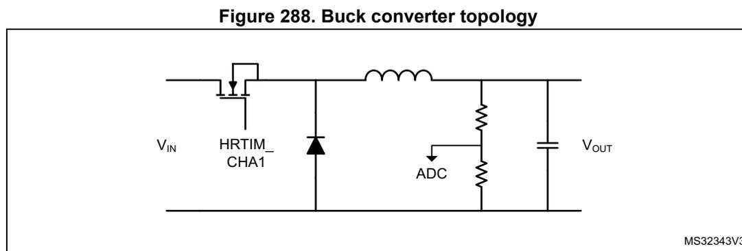
Figure 288. Buck converter topology
Figure 289 presents the management of two converters with identical frequency PWM signals. The outputs are defined as follows:
- • HRTIM_CHA1 set on period, reset on CMP1
- • HRTIM_CHA2 set on CMP3, reset on PER
The ADC is triggered twice per period, precisely in the middle of the ON time, using CMP2 and CMP4 events.
Figure 289. Dual Buck converter management
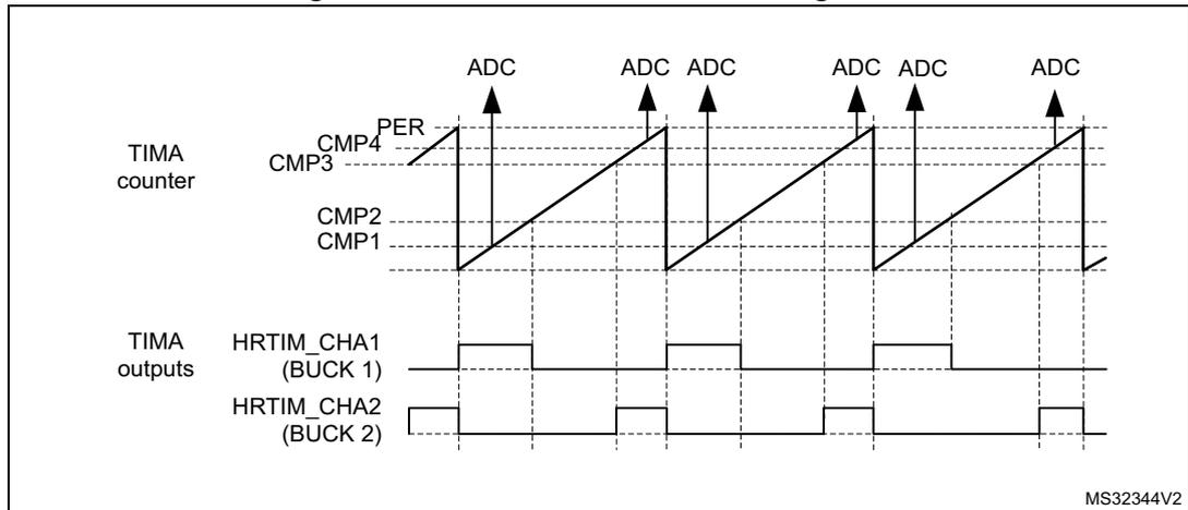
Timers A..E provide either 12 buck converters coupled by pairs (both with identical switching frequencies) or 7 completely independent converters (each of them having a different switching frequency), using the master timer as the 7 th time base.
28.4.2 Buck converter with synchronous rectification
Synchronous rectification allows to minimize losses in buck converters, by means of a FET replacing the freewheeling diode. Synchronous rectification can be turned on or off on the fly depending on the output current level, as shown on Figure 290 .
Figure 290. Synchronous rectification depending on output current
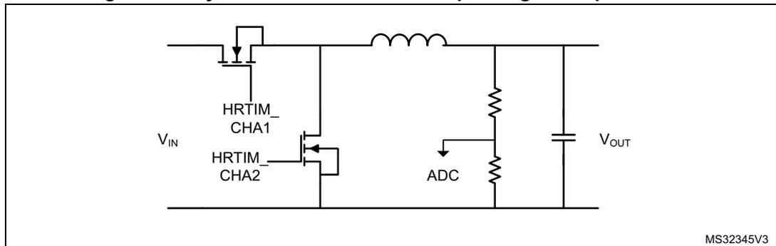
The main difference versus a single-switch buck converter is the addition of a deadtime for an almost complementary waveform generation on HRTIM_CHA2, based on the reference waveform on HRTIM_CHA1 (see Figure 291 ).
Figure 291. Buck with synchronous rectification
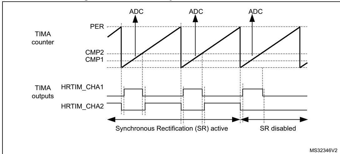
28.4.3 Multiphase converters
Multiphase techniques can be applied to multiple power conversion topologies (buck, flyback). Their main benefits are:
- • Reduction of the current ripple on the input and output capacitors
- • Reduced EMI
- • Higher efficiency at light load by dynamically changing the number of phases (phase shedding)
The HRTIM manages multiple converters. The number of converters that can be controlled depends on the topologies and resources used (including the ADC triggers):
- • 5 buck converters with synchronous rectification (SR), using the master timer and the 5 timers
- • 4 buck converters (without SR), using the master timer and 2 timers
Figure 292 presents the topology of a 3-phase interleaved buck converter.
Figure 292. 3-phase interleaved buck converter
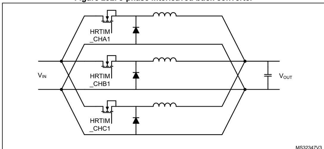
The master timer is responsible for the phase management: it defines the phase relationship between the converters by resetting the timers periodically. The phase-shift is \( 360^\circ \) divided by the number of phases, \( 120^\circ \) in the given example.
The duty cycle is then programmed into each of the timers. The outputs are defined as follows:
- – HRTIM_CHA1 set on master timer period, reset on TACMP1
- – HRTIM_CHB1 set on master timer MCMP1, reset on TBCMP1
- – HRTIM_CHC1 set on master timer MCMP2, reset on TCCMP1
The ADC trigger can be generated on TxCMP2 compare event. Since all ADC trigger sources are phase-shifted because of the converter topology, it is possible to have all of them combined into a single ADC trigger to save ADC resources (for instance 1 ADC regular channel for the full multi-phase converter).
Figure 293. 3-phase interleaved buck converter control
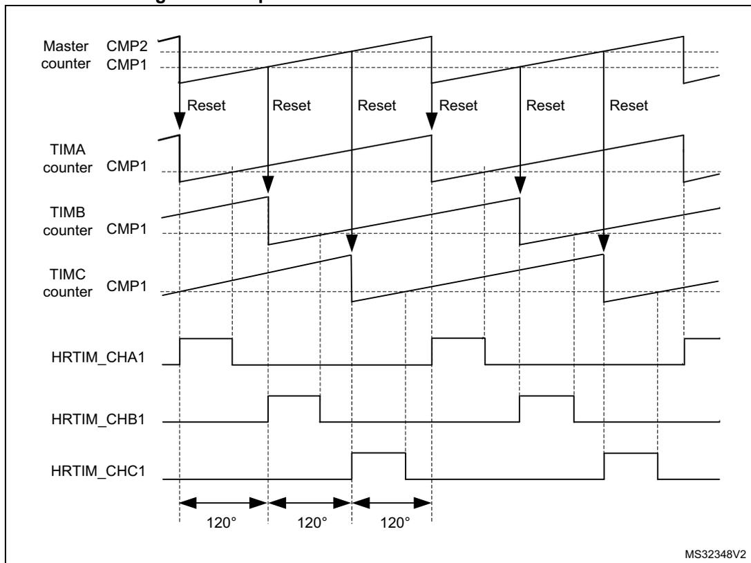
The figure is a timing diagram illustrating the control of a 3-phase interleaved buck converter. It shows the following signals and their relationships:
- Master counter: Shows a sawtooth waveform. It is reset by the CMP2 compare event. The CMP1 compare event is used to reset the phase counters.
- TIMA counter: Shows a sawtooth waveform. It is reset by the Master counter's CMP1 compare event. The CMP1 compare event is used to reset HRTIM_CHB1.
- TIMB counter: Shows a sawtooth waveform. It is reset by the Master counter's CMP1 compare event. The CMP1 compare event is used to reset HRTIM_CHC1.
- TIMC counter: Shows a sawtooth waveform. It is reset by the Master counter's CMP1 compare event. The CMP1 compare event is used to reset HRTIM_CHA1.
- HRTIM_CHA1: Output signal. It is set by the Master counter's CMP2 compare event and reset by the TIMC counter's CMP1 compare event.
- HRTIM_CHB1: Output signal. It is set by the Master counter's CMP2 compare event and reset by the TIMA counter's CMP1 compare event.
- HRTIM_CHC1: Output signal. It is set by the Master counter's CMP2 compare event and reset by the TIMB counter's CMP1 compare event.
The phase shift between the outputs is \( 120^\circ \) , as indicated by the arrows at the bottom of the diagram. The diagram is labeled MS32348V2.
28.4.4 Transition mode power factor correction
The basic operating principle is to build up current into an inductor during a fixed \( T_{on} \) time. This current then decays during the \( T_{off} \) time, and the period is re-started when it becomes null. This is detected using a Zero Crossing Detection circuitry (ZCD), as shown on Figure 294 . With a constant \( T_{on} \) time, the peak current value in the inductor is proportional to the rectified AC input voltage, which provides the power factor correction.
Figure 294. Transition mode PFC
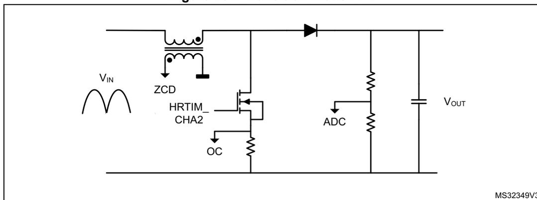
This converter operates with a constant \( T_{on} \) time and a variable frequency due to the \( T_{off} \) time variation (depending on the input voltage). It must also include some features to operate when no zero-crossing is detected, or to limit the \( T_{on} \) time in case of over-current (OC). The OC feedback is usually conditioned with the built-in comparator and routed onto an external event input.
Figure 295 presents the waveform during the various operating modes, with the following defined parameters:
- • \( T_{on} \) Min: masks spurious overcurrent (freewheeling diode recovery current), represented as OC blanking
- • \( T_{on} \) Max: practically, the converter set-point. It is defined by CMP1
- • \( T_{off} \) Min: limits the frequency when the current limit is close to zero (demagnetization is very fast). It is defined with CMP2.
- • \( T_{off} \) Max: prevents the system to be stuck if no ZCD occurs. It is defined with CMP4 in auto-delayed mode.
Both \( T_{off} \) values are auto-delayed since the value must be relative to the output falling edge.
Figure 295. Transition mode PFC waveforms
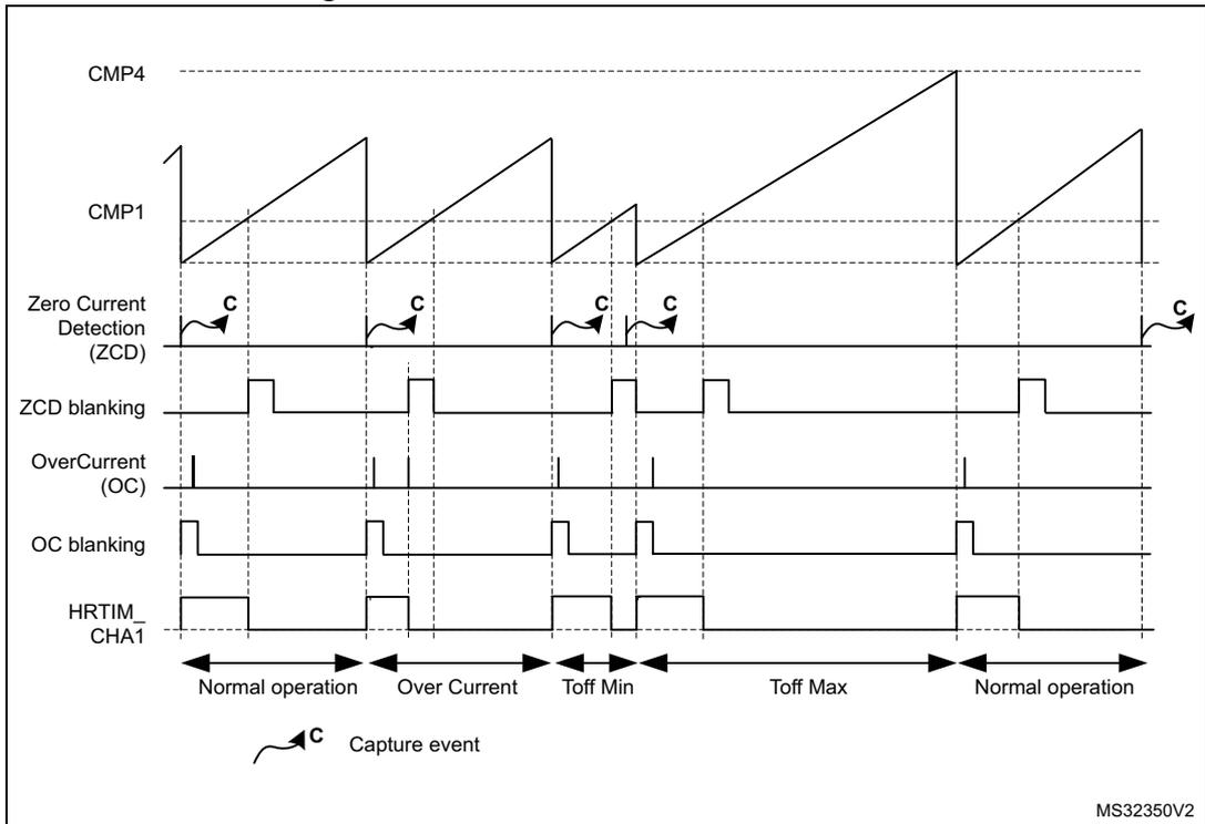
The figure displays seven timing waveforms over time, categorized into five operational periods: Normal operation, Over Current, Toff Min, Toff Max, and Normal operation. The waveforms are:
- CMP4: A constant high reference voltage level.
- CMP1: A sawtooth-like waveform that ramps up and is reset by the HRTIM_CHA1 signal.
- Zero Current Detection (ZCD): A signal that pulses low when the current is zero. Capture events (C) are indicated at the rising edges of these pulses.
- ZCD blanking: A signal that is high during the ZCD pulse duration to prevent multiple captures.
- OverCurrent (OC): A signal that pulses low when the current exceeds a threshold.
- OC blanking: A signal that is high during the OC pulse duration.
- HRTIM_CHA1: The output signal that controls the ramping of CMP1.
Operation periods and their characteristics:
- Normal operation: The initial and final periods where the system operates within standard limits.
- Over Current: A period where the current is high, causing the OC signal to pulse.
- Toff Min: A period where the HRTIM_CHA1 off-time is minimized.
- Toff Max: A period where the HRTIM_CHA1 off-time is maximized.
A legend at the bottom left shows a 'C' with a curved arrow pointing to a rising edge, labeled 'Capture event'.
MS32350V2
28.5 HRTIM registers
28.5.1 HRTIM master timer control register (HRTIM_MCR)
Address offset: 0x000
Reset value: 0x0000 0000
| 31 | 30 | 29 | 28 | 27 | 26 | 25 | 24 | 23 | 22 | 21 | 20 | 19 | 18 | 17 | 16 |
|---|---|---|---|---|---|---|---|---|---|---|---|---|---|---|---|
| BRSTDMA[1:0] | MREPU | Res. | PREEN | DACSYNC[1:0] | Res. | Res. | TFCEN | TECEN | TDCEN | TCCEN | TBCEN | TACEN | MCEN | ||
| rw | rw | rw | rw | rw | rw | rw | rw | rw | rw | rw | rw | rw | |||
| 15 | 14 | 13 | 12 | 11 | 10 | 9 | 8 | 7 | 6 | 5 | 4 | 3 | 2 | 1 | 0 |
|---|---|---|---|---|---|---|---|---|---|---|---|---|---|---|---|
| SYNCSRC[1:0] | SYNCOUT[1:0] | SYNCS TRTM | SYNCR STM | SYNCIN[1:0] | INTLVD[1:0] | HALF | RE TRIG | CONT | CKPSC[2:0] | ||||||
| rw | rw | rw | rw | rw | rw | rw | rw | rw | rw | rw | rw | rw | rw | rw | rw |
Bits 31:30 BRSTDMA[1:0]: Burst DMA update
These bits define how the update occurs relatively to a burst DMA transaction.
- 00: Update done independently from the DMA burst transfer completion
- 01: Update done when the DMA burst transfer is completed
- 10: Update done on master timer roll-over following a DMA burst transfer completion. This mode only works in continuous mode.
- 11: Reserved
Bit 29 MREPU: Master timer repetition update
This bit defines whether an update occurs when the master timer repetition period is completed (either due to roll-over or reset events). MREPU can be set only if BRSTDMA[1:0] = 00 or 01.
- 0: Update on repetition disabled
- 1: Update on repetition enabled
Bit 28 Reserved, must be kept at reset value.
Bit 27 PREEN: Preload enable
This bit enables the registers preload mechanism and defines whether the write accesses to the memory mapped registers are done into HRTIM’s active or preload registers.
- 0: Preload disabled: the write access is directly done into the active register
- 1: Preload enabled: the write access is done into the preload register
Bits 26:25 DACSYNC[1:0]: DAC synchronization
A DAC synchronization event can be enabled and generated when the master timer update occurs.
These bits are defining on which output the DAC synchronization is sent (refer to Section 28.3.21: DAC triggers for connections details).
- 00: No DAC trigger generated
- 01: Trigger generated on hrtim_dac_trg1
- 10: Trigger generated on hrtim_dac_trg2
- 11: Trigger generated on hrtim_dac_trg3
Bits 24:23 Reserved, must be kept at reset value.
Bit 22 TFCEN: Timer F counter enable
This bit starts the timer F counter.
- 0: Timer F counter disabled
- 1: Timer F counter enabled
Note: This bit must not be changed within a minimum of 8 cycles of f HRTIM clock.
Bit 21 TECEN : Timer E counter enableThis bit starts the timer E counter.
0: Timer E counter disabled
1: Timer E counter enabled
Note: This bit must not be changed within a minimum of 8 cycles of \( f_{HRTIM} \) clock.
Bit 20 TDCEN : Timer D counter enableThis bit starts the timer D counter.
0: Timer D counter disabled
1: Timer D counter enabled
Note: This bit must not be changed within a minimum of 8 cycles of \( f_{HRTIM} \) clock.
Bit 19 TCCEN : Timer C counter enableThis bit starts the timer C counter.
0: Timer C counter disabled
1: Timer C counter enabled
Note: This bit must not be changed within a minimum of 8 cycles of \( f_{HRTIM} \) clock.
Bit 18 TBCEN : Timer B counter enableThis bit starts the timer B counter.
0: Timer B counter disabled
1: Timer B counter enabled
Note: This bit must not be changed within a minimum of 8 cycles of \( f_{HRTIM} \) clock.
Bit 17 TACEN : Timer A counter enableThis bit starts the timer A counter.
0: Timer A counter disabled
1: Timer A counter enabled
Note: This bit must not be changed within a minimum of 8 cycles of \( f_{HRTIM} \) clock.
Bit 16 MCEN : Master timer counter enableThis bit starts the master timer counter.
0: Master counter disabled
1: Master counter enabled
Note: This bit must not be changed within a minimum of 8 cycles of \( f_{HRTIM} \) clock.
Bits 15:14 SYNCSRC[1:0] : Synchronization sourceThese bits define the source and event to be sent on the synchronization outputs SYNCOUT[2:1]
00: Master timer start
01: Master timer compare 1 event
10: Timer A start/reset
11: Timer A compare 1 event
Bits 13:12 SYNCOUT[1:0] : Synchronization outputThese bits define the routing and conditioning of the synchronization output event.
00: Disabled
01: Reserved
10: Positive pulse on HRTIM_SCOUT output (16x \( f_{HRTIM} \) clock cycles)
11: Negative pulse on HRTIM_SCOUT output (16x \( f_{HRTIM} \) clock cycles)
Note: This bitfield must not be modified once the counter is enabled (TxCEN bit set)
Bit 11 SYNCSTRM : Synchronization starts masterThis bit enables the master timer start when receiving a synchronization input event:
0: No effect on the master timer
1: A synchronization input event starts the master timer
Bit 10 SYNCRSTM: Synchronization resets master
This bit enables the master timer reset when receiving a synchronization input event:
0: No effect on the master timer
1: A synchronization input event resets the master timer
Bits 9:8 SYNCIN[1:0]: Synchronization input
These bits are defining the synchronization input source.
00: Disabled. HRTIM is not synchronized and runs in standalone mode.
01: Reserved
10: Internal event on hrtim_in_sync[2]: the HRTIM is synchronized with the on-chip timer (see
Section : Synchronization input
).
11: External event on hrtim_in_sync[3]: a positive pulse on HRTIM_SCIN input triggers the HRTIM.
Note: This parameter cannot be changed once the impacted timers are enabled.
Bits 7:6 INTLVD[1:0]: Interleaved mode
This bitfield is significant only when the HALF bit is reset. It enables the interleaved mode.
00: Interleaved mode disabled
01: Triple interleaved mode: when HRTIM_MPER register is written, the HRTIM_MCMP1R active register is automatically updated with HRTIM_MPER/3 value, and the HRTIM_MCMP2R active register is automatically updated with 2x (HRTIM_MPER/3) value.
10: Quad interleaved mode: when HRTIM_MPER register is written, the HRTIM_MCMP1R active register is automatically updated with HRTIM_MPER/4 value, the HRTIM_MCMP2R active register is automatically updated with HRTIM_MPER/2 value and the HRTIM_MCMP3R active register is automatically updated with 3x (HRTIM_MPER/4) value.
11: Interleaved mode disabled
Bit 5 HALF: Half mode
This bit enables the half duty-cycle mode: the HRTIM_MCMP1R active register is automatically updated with HRTIM_MPER/2 value when HRTIM_MPER register is written.
0: Half mode disabled
1: Half mode enabled
Bit 4 RETRIG: Re-triggerable mode
This bit defines the behavior of the master timer counter in single-shot mode.
0: The timer is not re-triggerable: a counter reset can be done only if the counter is stopped (period elapsed)
1: The timer is re-triggerable: a counter reset is done whatever the counter state (running or stopped)
Bit 3 CONT: Continuous mode
0: The timer operates in single-shot mode and stops when it reaches the MPER value
1: The timer operates in continuous (free-running) mode and rolls over to zero when it reaches the MPER value
Bits 2:0 CKPSC[2:0]: Clock prescaler
These bits define the master timer high-resolution clock prescaler ratio.
The counter clock equivalent frequency (
\(
f_{COUNTER}
\)
) is equal to
\(
f_{HRCK} / 2^{CKPSC[2:0]}
\)
.
The prescaling ratio cannot be modified once the timer is enabled.
28.5.2 HRTIM master timer interrupt status register (HRTIM_MISR)
Address offset: 0x004
Reset value: 0x0000 0000
| 31 | 30 | 29 | 28 | 27 | 26 | 25 | 24 | 23 | 22 | 21 | 20 | 19 | 18 | 17 | 16 |
|---|---|---|---|---|---|---|---|---|---|---|---|---|---|---|---|
| Res. | Res. | Res. | Res. | Res. | Res. | Res. | Res. | Res. | Res. | Res. | Res. | Res. | Res. | Res. | Res. |
| 15 | 14 | 13 | 12 | 11 | 10 | 9 | 8 | 7 | 6 | 5 | 4 | 3 | 2 | 1 | 0 |
| Res. | Res. | Res. | Res. | Res. | Res. | Res. | Res. | Res. | MUPD | SYNC | MREP | MCMP 4 | MCMP 3 | MCMP 2 | MCMP 1 |
| r | r | r | r | r | r | r |
Bits 31:7 Reserved, must be kept at reset value.
Bit 6 MUPD : Master update interrupt flag
This bit is set by hardware when the master timer registers are updated.
0: No master update interrupt occurred
1: Master update interrupt occurred
Bit 5 SYNC : Sync input interrupt flag
This bit is set by hardware when a synchronization input event is received.
0: No sync input interrupt occurred
1: Sync input interrupt occurred
Bit 4 MREP : Master repetition interrupt flag
This bit is set by hardware when the master timer repetition period has elapsed.
0: No master repetition interrupt occurred
1: Master repetition interrupt occurred
Bit 3 MCMP4 : Master compare 4 interrupt flag
Refer to MCMP1 description
Bit 2 MCMP3 : Master compare 3 interrupt flag
Refer to MCMP1 description
Bit 1 MCMP2 : Master compare 2 interrupt flag
Refer to MCMP1 description
Bit 0 MCMP1 : Master compare 1 interrupt flag
This bit is set by hardware when the master timer counter matches the value programmed in the master compare 1 register.
0: No master compare 1 interrupt occurred
1: Master compare 1 interrupt occurred
28.5.3 HRTIM master timer interrupt clear register (HRTIM_MICR)
Address offset: 0x008
Reset value: 0x0000 0000
| 31 | 30 | 29 | 28 | 27 | 26 | 25 | 24 | 23 | 22 | 21 | 20 | 19 | 18 | 17 | 16 |
|---|---|---|---|---|---|---|---|---|---|---|---|---|---|---|---|
| Res. | Res. | Res. | Res. | Res. | Res. | Res. | Res. | Res. | Res. | Res. | Res. | Res. | Res. | Res. | Res. |
| 15 | 14 | 13 | 12 | 11 | 10 | 9 | 8 | 7 | 6 | 5 | 4 | 3 | 2 | 1 | 0 |
| Res. | Res. | Res. | Res. | Res. | Res. | Res. | Res. | Res. | MUPDC C | SYNCC | MREPC C | MCMP4C | MCMP3C | MCMP2C | MCMP1C |
| w | w | w | w | w | w | w |
Bits 31:7 Reserved, must be kept at reset value.
Bit 6 MUPDC : Master update interrupt flag clear
Writing 1 to this bit clears the MUPDC flag in HRTIM_MISR register.
Bit 5 SYNCC : Sync input interrupt flag clear
Writing 1 to this bit clears the SYNC flag in HRTIM_MISR register.
Bit 4 MREPC : Repetition interrupt flag clear
Writing 1 to this bit clears the MREP flag in HRTIM_MISR register.
Bit 3 MCMP4C : Master compare 4 interrupt flag clear
Writing 1 to this bit clears the MCMP4 flag in HRTIM_MISR register.
Bit 2 MCMP3C : Master compare 3 interrupt flag clear
Writing 1 to this bit clears the MCMP3 flag in HRTIM_MISR register.
Bit 1 MCMP2C : Master compare 2 interrupt flag clear
Writing 1 to this bit clears the MCMP2 flag in HRTIM_MISR register.
Bit 0 MCMP1C : Master compare 1 interrupt flag clear
Writing 1 to this bit clears the MCMP1 flag in HRTIM_MISR register.
28.5.4 HRTIM master timer DMA interrupt enable register (HRTIM_MDIER)
Address offset: 0x00C
Reset value: 0x0000 0000
| 31 | 30 | 29 | 28 | 27 | 26 | 25 | 24 | 23 | 22 | 21 | 20 | 19 | 18 | 17 | 16 |
|---|---|---|---|---|---|---|---|---|---|---|---|---|---|---|---|
| Res. | Res. | Res. | Res. | Res. | Res. | Res. | Res. | Res. | MUPD DE | SYNCD E | MREP DE | MCMP 4DE | MCMP 3DE | MCMP 2DE | MCMP 1DE |
| rw | rw | rw | rw | rw | rw | rw |
| 15 | 14 | 13 | 12 | 11 | 10 | 9 | 8 | 7 | 6 | 5 | 4 | 3 | 2 | 1 | 0 |
|---|---|---|---|---|---|---|---|---|---|---|---|---|---|---|---|
| Res. | Res. | Res. | Res. | Res. | Res. | Res. | Res. | Res. | MUPDI E | SYNCI E | MREPI E | MCMP 4IE | MCMP 3IE | MCMP 2IE | MCMP 1IE |
| rw | rw | rw | rw | rw | rw | rw |
Bits 31:23 Reserved, must be kept at reset value.
Bit 22 MUPDDE : Master update DMA request enable
This bit is set and cleared by software to enable/disable the master update DMA requests.
0: Master update DMA request disabled
1: Master update DMA request enabled
Bit 21 SYNCDE : Sync input DMA request enable
This bit is set and cleared by software to enable/disable the sync input DMA requests.
0: Sync input DMA request disabled
1: Sync input DMA request enabled
Bit 20 MREPDE : Master repetition DMA request enable
This bit is set and cleared by software to enable/disable the master timer repetition DMA requests.
0: Repetition DMA request disabled
1: Repetition DMA request enabled
Bit 19 MCMP4DE : Master compare 4 DMA request enable
Refer to MCMP1DE description
Bit 18 MCMP3DE : Master compare 3 DMA request enable
Refer to MCMP1DE description
Bit 17 MCMP2DE : Master compare 2 DMA request enable
Refer to MCMP1DE description
Bit 16 MCMP1DE : Master compare 1 DMA request enable
This bit is set and cleared by software to enable/disable the master timer compare 1 DMA requests.
0: Compare 1 DMA request disabled
1: Compare 1 DMA request enabled
Bits 15:7 Reserved, must be kept at reset value.
Bit 6 MUPDIE : Master update interrupt enable
This bit is set and cleared by software to enable/disable the master timer registers update interrupts
0: Master update interrupts disabled
1: Master update interrupts enabled
Bit 5 SYNCIE : Sync input interrupt enable
This bit is set and cleared by software to enable/disable the sync input interrupts
0: Sync input interrupts disabled
1: Sync input interrupts enabled
Bit 4 MREPIE : Master repetition interrupt enable
This bit is set and cleared by software to enable/disable the master timer repetition interrupts
0: Master repetition interrupt disabled
1: Master repetition interrupt enabled
Bit 3 MCMP4IE : Master compare 4 interrupt enable
Refer to MCMP1IE description
Bit 2 MCMP3IE : Master compare 3 interrupt enable
Refer to MCMP1IE description
Bit 1 MCMP2IE : Master compare 2 interrupt enable
Refer to MCMP1IE description
Bit 0 MCMP1IE : Master compare 1 interrupt enable
This bit is set and cleared by software to enable/disable the master timer compare 1 interrupt
0: Compare 1 interrupt disabled
1: Compare 1 interrupt enabled
28.5.5 HRTIM master timer counter register (HRTIM_MCNTR)
Address offset: 0x010
Reset value: 0x0000 0000
| 31 | 30 | 29 | 28 | 27 | 26 | 25 | 24 | 23 | 22 | 21 | 20 | 19 | 18 | 17 | 16 |
|---|---|---|---|---|---|---|---|---|---|---|---|---|---|---|---|
| Res. | Res. | Res. | Res. | Res. | Res. | Res. | Res. | Res. | Res. | Res. | Res. | Res. | Res. | Res. | Res. |
| 15 | 14 | 13 | 12 | 11 | 10 | 9 | 8 | 7 | 6 | 5 | 4 | 3 | 2 | 1 | 0 |
| rw | rw | rw | rw | rw | rw | rw | rw | rw | rw | rw | rw | rw | rw | rw | rw |
| MCNT[15:0] | |||||||||||||||
Bits 31:16 Reserved, must be kept at reset value.
Bits 15:0 MCNT[15:0] : Counter value
Holds the master timer counter value. This register can only be written when the master timer is stopped (MCEN = 0 in HRTIM_MCR).
Note: For HR clock prescaling ratio below 32 (CKPSC[2:0] < 5), the least significant bits of the counter are not significant. They cannot be written and return 0 when read.
Note: The timer behavior is not guaranteed if the counter value is set above the HRTIM_MPER register value.
28.5.6 HRTIM master timer period register (HRTIM_MPER)
Address offset: 0x014
Reset value: 0x0000 FFDF
| 31 | 30 | 29 | 28 | 27 | 26 | 25 | 24 | 23 | 22 | 21 | 20 | 19 | 18 | 17 | 16 |
|---|---|---|---|---|---|---|---|---|---|---|---|---|---|---|---|
| Res. | Res. | Res. | Res. | Res. | Res. | Res. | Res. | Res. | Res. | Res. | Res. | Res. | Res. | Res. | Res. |
| 15 | 14 | 13 | 12 | 11 | 10 | 9 | 8 | 7 | 6 | 5 | 4 | 3 | 2 | 1 | 0 |
| rw | rw | rw | rw | rw | rw | rw | rw | rw | rw | rw | rw | rw | rw | rw | rw |
| MPER[15:0] | |||||||||||||||
Bits 31:16 Reserved, must be kept at reset value.
Bits 15:0 MPER[15:0] : Master timer period value
This register defines the counter overflow value.
The period value must be above or equal to 3 periods of the \( f_{HRTIM} \) clock, that is 0x60 if CKPSC[2:0] = 0, 0x30 if CKPSC[2:0] = 1, 0x18 if CKPSC[2:0] = 2, ...
The maximum value is 0x0000 FFDF.
28.5.7 HRTIM master timer repetition register (HRTIM_MREP)
Address offset: 0x018
Reset value: 0x0000 0000
| 31 | 30 | 29 | 28 | 27 | 26 | 25 | 24 | 23 | 22 | 21 | 20 | 19 | 18 | 17 | 16 |
|---|---|---|---|---|---|---|---|---|---|---|---|---|---|---|---|
| Res. | Res. | Res. | Res. | Res. | Res. | Res. | Res. | Res. | Res. | Res. | Res. | Res. | Res. | Res. | Res. |
| 15 | 14 | 13 | 12 | 11 | 10 | 9 | 8 | 7 | 6 | 5 | 4 | 3 | 2 | 1 | 0 |
| Res. | Res. | Res. | Res. | Res. | Res. | Res. | Res. | MREP[7:0] | |||||||
| rw | rw | rw | rw | rw | rw | rw | rw | ||||||||
Bits 31:8 Reserved, must be kept at reset value.
Bits 7:0 MREP[7:0] : Master timer repetition period value
This register holds the repetition period value for the master counter. It is either the preload register or the active register if preload is disabled.
28.5.8 HRTIM master timer compare 1 register (HRTIM_MCMP1R)
Address offset: 0x01C
Reset value: 0x0000 0000
| 31 | 30 | 29 | 28 | 27 | 26 | 25 | 24 | 23 | 22 | 21 | 20 | 19 | 18 | 17 | 16 |
|---|---|---|---|---|---|---|---|---|---|---|---|---|---|---|---|
| Res. | Res. | Res. | Res. | Res. | Res. | Res. | Res. | Res. | Res. | Res. | Res. | Res. | Res. | Res. | Res. |
| 15 | 14 | 13 | 12 | 11 | 10 | 9 | 8 | 7 | 6 | 5 | 4 | 3 | 2 | 1 | 0 |
| MCMP1[15:0] | |||||||||||||||
| rw | rw | rw | rw | rw | rw | rw | rw | rw | rw | rw | rw | rw | rw | rw | rw |
Bits 31:16 Reserved, must be kept at reset value.
Bits 15:0 MCMP1[15:0] : Master timer compare 1 value
This register holds the master timer compare 1 value. It is either the preload register or the active register if preload is disabled.
The compare value must be above or equal to 3 periods of the \( f_{HRTIM} \) clock, that is 0x60 if CKPSC[2:0] = 0, 0x30 if CKPSC[2:0] = 1, 0x18 if CKPSC[2:0] = 2,...
28.5.9 HRTIM master timer compare 2 register (HRTIM_MCMP2R)
Address offset: 0x024
Reset value: 0x0000 0000
| 31 | 30 | 29 | 28 | 27 | 26 | 25 | 24 | 23 | 22 | 21 | 20 | 19 | 18 | 17 | 16 |
|---|---|---|---|---|---|---|---|---|---|---|---|---|---|---|---|
| Res. | Res. | Res. | Res. | Res. | Res. | Res. | Res. | Res. | Res. | Res. | Res. | Res. | Res. | Res. | Res. |
| 15 | 14 | 13 | 12 | 11 | 10 | 9 | 8 | 7 | 6 | 5 | 4 | 3 | 2 | 1 | 0 |
| MCMP2[15:0] | |||||||||||||||
| rw | rw | rw | rw | rw | rw | rw | rw | rw | rw | rw | rw | rw | rw | rw | rw |
Bits 31:16 Reserved, must be kept at reset value.
Bits 15:0 MCMP2[15:0] : Master timer compare 2 value
This register holds the master timer compare 2 value. It is either the preload register or the active register if preload is disabled.
The compare value must be above or equal to 3 periods of the \( f_{HRTIM} \) clock, that is 0x60 if CKPSC[2:0] = 0, 0x30 if CKPSC[2:0] = 1, 0x18 if CKPSC[2:0] = 2,...
28.5.10 HRTIM master timer compare 3 register (HRTIM_MCMP3R)
Address offset: 0x028
Reset value: 0x0000 0000
| 31 | 30 | 29 | 28 | 27 | 26 | 25 | 24 | 23 | 22 | 21 | 20 | 19 | 18 | 17 | 16 |
|---|---|---|---|---|---|---|---|---|---|---|---|---|---|---|---|
| Res. | Res. | Res. | Res. | Res. | Res. | Res. | Res. | Res. | Res. | Res. | Res. | Res. | Res. | Res. | Res. |
| 15 | 14 | 13 | 12 | 11 | 10 | 9 | 8 | 7 | 6 | 5 | 4 | 3 | 2 | 1 | 0 |
| MCMP3[15:0] | |||||||||||||||
| rw | rw | rw | rw | rw | rw | rw | rw | rw | rw | rw | rw | rw | rw | rw | rw |
Bits 31:16 Reserved, must be kept at reset value.
Bits 15:0 MCMP3[15:0] : Master timer compare 3 value
This register holds the master timer compare 3 value. It is either the preload register or the active register if preload is disabled.
The compare value must be above or equal to 3 periods of the \( f_{HRTIM} \) clock, that is 0x60 if CKPSC[2:0] = 0, 0x30 if CKPSC[2:0] = 1, 0x18 if CKPSC[2:0] = 2,...
28.5.11 HRTIM master timer compare 4 register (HRTIM_MCMP4R)Address offset: 0x02C
Reset value: 0x0000 0000
| 31 | 30 | 29 | 28 | 27 | 26 | 25 | 24 | 23 | 22 | 21 | 20 | 19 | 18 | 17 | 16 |
|---|---|---|---|---|---|---|---|---|---|---|---|---|---|---|---|
| Res. | Res. | Res. | Res. | Res. | Res. | Res. | Res. | Res. | Res. | Res. | Res. | Res. | Res. | Res. | Res. |
| 15 | 14 | 13 | 12 | 11 | 10 | 9 | 8 | 7 | 6 | 5 | 4 | 3 | 2 | 1 | 0 |
| MCMP4[15:0] | |||||||||||||||
| rw | rw | rw | rw | rw | rw | rw | rw | rw | rw | rw | rw | rw | rw | rw | rw |
Bits 31:16 Reserved, must be kept at reset value.
Bits 15:0 MCMP4[15:0] : Master timer compare 4 value
This register holds the master timer compare 4 value. It is either the preload register or the active register if preload is disabled.
The compare value must be above or equal to 3 periods of the \( f_{HRTIM} \) clock, that is 0x60 if CKPSC[2:0] = 0, 0x30 if CKPSC[2:0] = 1, 0x18 if CKPSC[2:0] = 2,...
28.5.12 HRTIM timer x control register (HRTIM_TIMxCR) (x = A to F)
Address offset: Block A: 0x080
Address offset: Block B: 0x100
Address offset: Block C: 0x180
Address offset: Block D: 0x200
Address offset: Block E: 0x280
Address offset: Block F: 0x300
Reset value: 0x0000 0000
| 31 | 30 | 29 | 28 | 27 | 26 | 25 | 24 | 23 | 22 | 21 | 20 | 19 | 18 | 17 | 16 |
|---|---|---|---|---|---|---|---|---|---|---|---|---|---|---|---|
| UPDGAT[3:0] | PREEN | DACSYNC[1:0] | MSTU | TEU | TDU | TCU | TBU | TAU | TxRST U | TxREP U | TFU | ||||
| rw | rw | rw | rw | rw | rw | rw | rw | rw | rw | rw | rw | rw | rw | rw | rw |
| 15 | 14 | 13 | 12 | 11 | 10 | 9 | 8 | 7 | 6 | 5 | 4 | 3 | 2 | 1 | 0 |
|---|---|---|---|---|---|---|---|---|---|---|---|---|---|---|---|
| DELCMP4[1:0] | DELCMP2[1:0] | SYNCS TRTx | SYNCR STx | RSYNC U | INTLVD[1:0] | PSHPL L | HALF | RETRI G | CONT | CKPSCx[2:0] | |||||
| rw | rw | rw | rw | rw | rw | rw | rw | rw | rw | rw | rw | rw | rw | rw | rw |
Bits 31:28 UPDGAT[3:0]: Update gating
These bits define how the update occurs relatively to the burst DMA transaction and the external update request on update enable inputs hrtim_upd_en[3:1] (see Table 224 ).
The update events, as mentioned below, can be: MSTU, TFU, TEU, TDU, TCU, TBU, TAU, TxRSTU, TxREPU.
0000: The update occurs independently from the DMA burst transfer
0001: The update occurs when the DMA burst transfer is completed
0010: The update occurs on the update event following the DMA burst transfer completion
0011: The update occurs on a rising edge on hrtim_upd_en1
0100: The update occurs on a rising edge on hrtim_upd_en2
0101: The update occurs on a rising edge on hrtim_upd_en3
0110: The update occurs on the update event following a rising edge on hrtim_upd_en1
0111: The update occurs on the update event following a rising edge on hrtim_upd_en2
1000: The update occurs on the update event following a rising edge on hrtim_upd_en3
Others: Reserved
Note: This bitfield must be reset before programming a new value.
For UPDGAT[3:0] values equal to 0001, 0011, 0100, 0101, it is possible to have multiple concurrent update source (for instance RSTU and DMA burst).
Bit 27 PREEN: Preload enable
This bit enables the registers preload mechanism and defines whether a write access into a preloadable register is done into the active or the preload register.
0: Preload disabled: the write access is directly done into the active register
1: Preload enabled: the write access is done into the preload register
Bits 26:25 DACSYNC[1:0] : DAC synchronizationA DAC synchronization event is generated when the timer update occurs. These bits are defining on which output the DAC synchronization is sent (refer to Section 28.3.21: DAC triggers for connections details).
- 00: No DAC trigger generated
- 01: Trigger generated on hrtim_dac_trg1
- 10: Trigger generated on hrtim_dac_trg2
- 11: Trigger generated on hrtim_dac_trg3
Register update is triggered by the master timer update.
- 0: Update by master timer disabled
- 1: Update by master timer enabled
Register update is triggered by the timer E update
- 0: Update by timer E disabled
- 1: Update by timer E enabled
Note: This bit is reserved for HRTIM_TIMECR. It is only available for HRTIM_TIMACR, HRTIM_TIMBCR, HRTIM_TIMCCR, HRTIM_TIMDCR, HRTIM_TIMFCR.
Bit 22 TDU : Timer D updateRegister update is triggered by the timer D update
- 0: Update by timer D disabled
- 1: Update by timer D enabled
Note: This bit is reserved for HRTIM_TIMDCR. It is only available for HRTIM_TIMACR, HRTIM_TIMBCR, HRTIM_TIMCCR, HRTIM_TIMECR, HRTIM_TIMFCR.
Bit 21 TCU : Timer C updateRegister update is triggered by the timer C update
- 0: Update by timer C disabled
- 1: Update by timer C enabled
Note: This bit is reserved for HRTIM_TIMCCR. It is only available for HRTIM_TIMACR, HRTIM_TIMBCR, HRTIM_TIMDCR, HRTIM_TIMECR, HRTIM_TIMFCR.
Bit 20 TBU : Timer B updateRegister update is triggered by the timer B update
- 0: Update by timer B disabled
- 1: Update by timer B enabled
Note: This bit is reserved for HRTIM_TIMBCR. It is only available for HRTIM_TIMACR, HRTIM_TIMCCR, HRTIM_TIMDCR, HRTIM_TIMECR, HRTIM_TIMFCR.
Bit 19 TAU : Timer A updateRegister update is triggered by the timer A update
- 0: Update by timer A disabled
- 1: Update by timer A enabled
Note: This bit is reserved for HRTIM_TIMBCR. It is only available for HRTIM_TIMBCR, HRTIM_TIMCCR, HRTIM_TIMDCR, HRTIM_TIMECR, HRTIM_TIMFCR.
Bit 18 TxRSTU : Timer x reset updateRegister update is triggered by timer x counter reset or roll-over to 0 after reaching the period value in continuous mode.
- 0: Update by timer x reset / roll-over disabled
- 1: Update by timer x reset / roll-over enabled
Bit 17 TxREPU : Timer x repetition update
Register update is triggered when the counter rolls over and HRTIM_REPx = 0
0: Update on repetition disabled
1: Update on repetition enabled
Bit 16 TFU : Timer F update
Register update is triggered by the timer F update
0: Update by timer F disabled
1: Update by timer F enabled
Note: This bit is reserved for HRTIM_TIMFCR. It is only available for HRTIM_TIMACR, HRTIM_TIMBCR, HRTIM_TIMCCR, HRTIM_TIMDCR, HRTIM_TIMECR.
Bits 15:14 DEL CMP4[1:0] : CMP4 auto-delayed mode
This bitfield defines whether the compare register is behaving in standard mode (compare match issued as soon as counter equal compare), or in auto-delayed mode (see Section : Auto-delayed mode ).
00: CMP4 register is always active (standard compare mode)
01: CMP4 value is recomputed and is active following a capture 2 event
10: CMP4 value is recomputed and is active following a capture 2 event, or is recomputed and active after Compare 1 match (timeout function if capture 2 event is missing)
11: CMP4 value is recomputed and is active following a capture 2 event, or is recomputed and active after Compare 3 match (timeout function if capture event is missing)
Note: This bitfield must not be modified once the counter is enabled (TxCEN bit set).
Bits 13:12 DEL CMP2[1:0] : CMP2 auto-delayed mode
This bitfield defines whether the compare register is behaving in standard mode (compare match issued as soon as counter equal compare), or in auto-delayed mode (see Section : Auto-delayed mode ).
00: CMP2 register is always active (standard compare mode)
01: CMP2 value is recomputed and is active following a capture 1 event
10: CMP2 value is recomputed and is active following a capture 1 event, or is recomputed and active after compare 1 match (timeout function if capture event is missing)
11: CMP2 value is recomputed and is active following a capture 1 event, or is recomputed and active after compare 3 match (timeout function if capture event is missing)
Note: This bitfield must not be modified once the counter is enabled (TxCEN bit set).
Bit 11 SYNC STRTx : Synchronization starts timer x
This bit defines the timer x behavior following the synchronization event:
0: No effect on timer x
1: A synchronization input event starts the timer x
Bit 10 SYNCRSTx : Synchronization resets timer x
This bit defines the timer x behavior following the synchronization event:
0: No effect on timer x
1: A synchronization input event resets the timer x
Bit 9 RSYNCU : Re-synchronized update
This bit specifies whether update source coming outside from the timing unit must be synchronized:
0: The update coming from adjacent timers (when MSTU, TAU, TBU, TCU, TDU, TEU, TFU bit is set) or from a software update (TxSWU bit) is taken into account immediately
1: The update coming from adjacent timers (when MSTU, TAU, TBU, TCU, TDU, TEU, TFU bit is set) or from a software update (TxSWU bit) is taken into account on the following reset/roll-over event.
Note: This bit is significant only when UPDGAT[3:0] = 0000, it is ignored otherwise.
Bits 8:7 INTLVD[1:0] : Interleaved modeThis bitfield is significant only when the HALF bit is reset. It enables the interleaved mode.
00: Interleaved mode disabled
01: Triple interleaved mode: when HRTIM_PERxR register is written, the HRTIM_CMP1xR active register is automatically updated with HRTIM_PERxR/3 value, and the HRTIM_CMP2xR active register is automatically updated with 2x (HRTIM_PERxR/3) value.
10: Quad interleaved mode: when HRTIM_PERxR register is written, the HRTIM_CMP1xR active register is automatically updated with HRTIM_PERxR/4 value, the HRTIM_CMP2xR active register is automatically updated with HRTIM_PERxR/2 value and the HRTIM_CMP3xR active register is automatically updated with 3x (HRTIM_PERxR/4) value.
11: Interleaved mode disabled
Bit 6 PSHPLL : Push-pull mode enableThis bit enables the push-pull mode.
0: Push-pull mode disabled
1: Push-pull mode enabled
Note: This bitfield must not be modified once the counter is enabled (TxCEN bit set).
Bit 5 HALF : Half mode enableThis bit enables the half duty-cycle mode: the HRTIM_CMP1xR active register is automatically updated with HRTIM_PERxR/2 value when HRTIM_PERxR register is written.
0: Half mode disabled
1: Half mode enabled
Bit 4 RETRIG : Re-triggerable modeThis bit defines the counter behavior in single shot mode.
0: The timer is not re-triggerable: a counter reset is done if the counter is stopped (period elapsed in single-shot mode or counter stopped in continuous mode)
1: The timer is re-triggerable: a counter reset is done whatever the counter state.
Bit 3 CONT : Continuous modeThis bit defines the timer operating mode.
0: The timer operates in single-shot mode and stops when it reaches TIMxPER value
1: The timer operates in continuous mode and rolls over to zero when it reaches TIMxPER value
Bits 2:0 CKPSCx[2:0] : HRTIM timer x clock prescalerThese bits define the master timer high-resolution clock prescaler ratio.
The counter clock equivalent frequency ( \( f_{COUNTER} \) ) is equal to \( f_{HRCK} / 2^{CKPSC[2:0]} \) .
The prescaling ratio cannot be modified once the timer is enabled.
28.5.13 HRTIM timer x interrupt status register (HRTIM_TIMxISR) (x = A to F)
Address offset: Block A: 0x084
Address offset: Block B: 0x104
Address offset: Block C: 0x184
Address offset: Block D: 0x204
Address offset: Block E: 0x284
Address offset: Block F: 0x304
Reset value: 0x0000 0000
| 31 | 30 | 29 | 28 | 27 | 26 | 25 | 24 | 23 | 22 | 21 | 20 | 19 | 18 | 17 | 16 |
|---|---|---|---|---|---|---|---|---|---|---|---|---|---|---|---|
| Res. | Res. | Res. | Res. | Res. | Res. | Res. | Res. | Res. | Res. | O2CPY | O1CPY | O2 STAT | O1 STAT | IPP STAT | CPP STAT |
| r | r | r | r | r | r | ||||||||||
| 15 | 14 | 13 | 12 | 11 | 10 | 9 | 8 | 7 | 6 | 5 | 4 | 3 | 2 | 1 | 0 |
| Res. | DLYPR T | RST | RSTx2 | SETx2 | RSTx1 | SETx1 | CPT2 | CPT1 | UPD | Res. | REP | CMP4 | CMP3 | CMP2 | CMP1 |
| r | r | r | r | r | r | r | r | r | r | r | r | r | r |
Bits 31:22 Reserved, must be kept at reset value.
Bit 21 O2CPY : Output 2 copy
This status bit is a raw copy of the output 2 state, before the output stage (chopper, polarity). It allows to check the current output state before re-enabling the output after a delayed protection.
0: Output 2 is inactive
1: Output 2 is active
Bit 20 O1CPY : Output 1 copy
This status bit is a raw copy of the output 1 state, before the output stage (chopper, polarity). It allows to check the current output state before re-enabling the output after a delayed protection.
0: Output 1 is inactive
1: Output 1 is active
Bit 19 O2STAT : Output 2 status
This status bit indicates the output 2 state when the delayed idle protection was triggered. This bit is updated upon any new delayed protection entry. This bit is not updated in balanced idle.
0: Output 2 was inactive
1: Output 2 was active
Bit 18 O1STAT : Output 1 status
This status bit indicates the output 1 state when the delayed idle protection was triggered. This bit is updated upon any new delayed protection entry. This bit is not updated in balanced idle.
0: Output 1 was inactive
1: Output 1 was active
Bit 17 IPPSTAT : Idle push-pull Status
This status bit indicates on which output the signal was applied, in push-pull mode balanced fault mode or delayed idle mode, when the protection was triggered (whatever the output state, active or inactive).
0: Protection occurred when the output 1 was active and output 2 forced inactive
1: Protection occurred when the output 2 was active and output 1 forced inactive
Bit 16 CPPSTAT : Current push-pull status
This status bit indicates on which output the signal is currently applied, in push-pull mode. It is only significant in this configuration.
0: Signal applied on output 1 and output 2 forced inactive
1: Signal applied on output 2 and output 1 forced inactive
Bit 15 Reserved, must be kept at reset value.
Bit 14 DLYPRT : Delayed protection flag
0: No delayed protection interrupt occurred
1: Delayed Idle or balanced Idle mode entry occurred
Bit 13 RST : Reset and/or roll-over interrupt flag
This bit is set by hardware when the timer x counter is reset or rolls over in continuous mode.
0: No TIMx counter reset/roll-over interrupt occurred
1: TIMx counter reset/roll-over interrupt occurred
Bit 12 RSTx2 : Output 2 reset interrupt flag timer x
Refer to RSTx1 description
Bit 11 SETx2 : Output 2 set interrupt flag timer x
Refer to SETx1 description
Bit 10 RSTx1 : Output 1 reset interrupt flag timer x
This bit is set by hardware when the Tx1 output is reset (goes from active to inactive mode).
0: No Tx1 output reset interrupt occurred
1: Tx1 output reset interrupt occurred
Bit 9 SETx1 : Output 1 set interrupt flag timer x
This bit is set by hardware when the Tx1 output is set (goes from inactive to active mode).
0: No Tx1 output set interrupt occurred
1: Tx1 output set interrupt occurred
Bit 8 CPT2 : Capture 2 interrupt flag
Refer to CPT1 description
Bit 7 CPT1 : Capture 1 interrupt flag
This bit is set by hardware when the timer x capture 1 event occurs.
0: No timer x capture 1 interrupt occurred
1: Timer x capture 1 interrupt occurred
Bit 6 UPD : Update interrupt flag
This bit is set by hardware when the timer x update event occurs.
0: No timer x update interrupt occurred
1: Timer x update interrupt occurred
Bit 5 Reserved, must be kept at reset value.
Bit 4 REP : Repetition interrupt flag
This bit is set by hardware when the timer x repetition period has elapsed.
0: No timer x repetition interrupt occurred
1: Timer x repetition interrupt occurred
Bit 3 CMP4 : Compare 4 interrupt flag
Refer to CMP1 description
- Bit 2
CMP3
: Compare 3 interrupt flag
Refer to CMP1 description - Bit 1
CMP2
: Compare 2 interrupt flag
Refer to CMP1 description - Bit 0
CMP1
: Compare 1 interrupt flag
This bit is set by hardware when the timer x counter matches the value programmed in the compare 1 register.
0: No compare 1 interrupt occurred
1: Compare 1 interrupt occurred
28.5.14 HRTIM timer x interrupt clear register (HRTIM_TIMxICR) (x = A to F)
Address offset: Block A: 0x088
Address offset: Block B: 0x108
Address offset: Block C: 0x188
Address offset: Block D: 0x208
Address offset: Block E: 0x288
Address offset: Block F: 0x308
Reset value: 0x0000 0000
| 31 | 30 | 29 | 28 | 27 | 26 | 25 | 24 | 23 | 22 | 21 | 20 | 19 | 18 | 17 | 16 |
|---|---|---|---|---|---|---|---|---|---|---|---|---|---|---|---|
| Res. | Res. | Res. | Res. | Res. | Res. | Res. | Res. | Res. | Res. | Res. | Res. | Res. | Res. | Res. | Res. |
| 15 | 14 | 13 | 12 | 11 | 10 | 9 | 8 | 7 | 6 | 5 | 4 | 3 | 2 | 1 | 0 |
| Res. | DLYPRTC | RSTC | RSTx2C | SETx2C | RSTx1C | SETx1C | CPT2C | CPT1C | UPDC | Res. | REPC | CMP4C | CMP3C | CMP2C | CMP1C |
| w | w | w | w | w | w | w | w | w | w | w | w | w | w |
Bits 31:15 Reserved, must be kept at reset value.
- Bit 14
DLYPRTC
: Delayed protection flag clear
Writing 1 to this bit clears the DLYPRT flag in HRTIM_TIMxISR register - Bit 13
RSTC
: Reset interrupt flag clear
Writing 1 to this bit clears the RST flag in HRTIM_TIMxISR register - Bit 12
RSTx2C
: Output 2 reset flag clear timer x
Writing 1 to this bit clears the RSTx2 flag in HRTIM_TIMxISR register - Bit 11
SETx2C
: Output 2 set flag clear timer x
Writing 1 to this bit clears the SETx2 flag in HRTIM_TIMxISR register - Bit 10
RSTx1C
: Output 1 reset flag clear timer x
Writing 1 to this bit clears the RSTx1 flag in HRTIM_TIMxISR register - Bit 9
SETx1C
: Output 1 set flag clear timer x
Writing 1 to this bit clears the SETx1 flag in HRTIM_TIMxISR register
- Bit 8
CPT2C
: Capture 2 interrupt flag clear
Writing 1 to this bit clears the CPT2 flag in HRTIM_TIMxISR register - Bit 7
CPT1C
: Capture 1 interrupt flag clear
Writing 1 to this bit clears the CPT1 flag in HRTIM_TIMxISR register - Bit 6
UPDC
: Update interrupt flag clear
Writing 1 to this bit clears the UPD flag in HRTIM_TIMxISR register - Bit 5 Reserved, must be kept at reset value.
- Bit 4
REPC
: Repetition interrupt flag clear
Writing 1 to this bit clears the REP flag in HRTIM_TIMxISR register - Bit 3
CMP4C
: Compare 4 interrupt flag clear
Writing 1 to this bit clears the CMP4 flag in HRTIM_TIMxISR register - Bit 2
CMP3C
: Compare 3 interrupt flag clear
Writing 1 to this bit clears the CMP3 flag in HRTIM_TIMxISR register - Bit 1
CMP2C
: Compare 2 interrupt flag clear
Writing 1 to this bit clears the CMP2 flag in HRTIM_TIMxISR register - Bit 0
CMP1C
: Compare 1 interrupt flag clear
Writing 1 to this bit clears the CMP1 flag in HRTIM_TIMxISR register
28.5.15 HRTIM timer x DMA interrupt enable register (HRTIM_TIMxDIER) (x = A to F)
Address offset: Block A: 0x08C
Address offset: Block B: 0x10C
Address offset: Block C: 0x18C
Address offset: Block D: 0x20C
Address offset: Block E: 0x28C
Address offset: Block F: 0x30C
Reset value: 0x0000 0000
| 31 | 30 | 29 | 28 | 27 | 26 | 25 | 24 | 23 | 22 | 21 | 20 | 19 | 18 | 17 | 16 |
|---|---|---|---|---|---|---|---|---|---|---|---|---|---|---|---|
| Res. | DLYPR TDE | RSTDE | RSTx2 DE | SETx2 DE | RSTx1 DE | SETx1 DE | CPT2D E | CPT1D E | UPDDE | Res. | REPDE | CMP4D E | CMP3D E | CMP2D E | CMP1D E |
| rw | rw | rw | rw | rw | rw | rw | rw | rw | rw | rw | rw | rw | rw | ||
| 15 | 14 | 13 | 12 | 11 | 10 | 9 | 8 | 7 | 6 | 5 | 4 | 3 | 2 | 1 | 0 |
| Res. | DLYPR TIE | RSTIE | RSTx2I E | SETx2I E | RSTx1I E | SETx1I E | CPT2IE | CPT1IE | UPDIE | Res. | REPIE | CMP4I E | CMP3I E | CMP2I E | CMP1I E |
| rw | rw | rw | rw | rw | rw | rw | rw | rw | rw | rw | rw | rw | rw |
- Bit 31 Reserved, must be kept at reset value.
- Bit 30
DLYPRTDE
: Delayed protection DMA request enable
This bit is set and cleared by software to enable/disable DMA requests on delayed protection.
0: Delayed protection DMA request disabled
1: Delayed protection DMA request enabled - Bit 29
RSTDE
: Reset/roll-over DMA request enable
This bit is set and cleared by software to enable/disable DMA requests on timer x counter reset or roll-over in continuous mode.
0: Timer x counter reset/roll-over DMA request disabled
1: Timer x counter reset/roll-over DMA request enabled - Bit 28
RSTx2DE
: Output 2 reset DMA request enable timer x
Refer to RSTx1DE description - Bit 27
SETx2DE
: Output 2 set DMA request enable timer x
Refer to SETx1DE description - Bit 26
RSTx1DE
: Output 1 reset DMA request enable timer x
This bit is set and cleared by software to enable/disable Tx1 output reset DMA requests.
0: Tx1 output reset DMA request disabled
1: Tx1 output reset DMA request enabled - Bit 25
SETx1DE
: Output 1 set DMA request enable timer x
This bit is set and cleared by software to enable/disable Tx1 output set DMA requests.
0: Tx1 output set DMA request disabled
1: Tx1 output set DMA request enabled - Bit 24
CPT2DE
: Capture 2 DMA request enable
Refer to CPT1DE description - Bit 23
CPT1DE
: Capture 1 DMA request enable
This bit is set and cleared by software to enable/disable capture 1 DMA requests.
0: Capture 1 DMA request disabled
1: Capture 1 DMA request enabled - Bit 22
UPDDE
: Update DMA request enable
This bit is set and cleared by software to enable/disable DMA requests on update event.
0: Update DMA request disabled
1: Update DMA request enabled - Bit 21 Reserved, must be kept at reset value.
- Bit 20
REPDE
: Repetition DMA request enable
This bit is set and cleared by software to enable/disable DMA requests on repetition event.
0: Repetition DMA request disabled
1: Repetition DMA request enabled - Bit 19
CMP4DE
: Compare 4 DMA request enable
Refer to CMP1DE description - Bit 18
CMP3DE
: Compare 3 DMA request enable
Refer to CMP1DE description - Bit 17
CMP2DE
: Compare 2 DMA request enable
Refer to CMP1DE description
- Bit 16
CMP1DE
: Compare 1 DMA request enable
This bit is set and cleared by software to enable/disable the compare 1 DMA requests.
0: Compare 1 DMA request disabled
1: Compare 1 DMA request enabled - Bit 15 Reserved, must be kept at reset value.
- Bit 14
DLYPRTIE
: Delayed protection interrupt enable
This bit is set and cleared by software to enable/disable interrupts on delayed protection.
0: Delayed protection interrupts disabled
1: Delayed protection interrupts enabled - Bit 13
RSTIE
: Reset/roll-over interrupt enable
This bit is set and cleared by software to enable/disable interrupts on timer x counter reset or roll-over in continuous mode.
0: Timer x counter reset/roll-over interrupt disabled
1: Timer x counter reset/roll-over interrupt enabled - Bit 12
RSTx2IE
: Output 2 reset interrupt enable timer x
Refer to RSTx1IE description - Bit 11
SETx2IE
: Output 2 set interrupt enable timer x
Refer to SETx1IE description - Bit 10
RSTx1IE
: Output 1 reset interrupt enable timer x
This bit is set and cleared by software to enable/disable Tx1 output reset interrupts.
0: Tx1 output reset interrupts disabled
1: Tx1 output reset interrupts enabled - Bit 9
SETx1IE
: Output 1 set interrupt enable timer x
This bit is set and cleared by software to enable/disable Tx1 output set interrupts.
0: Tx1 output set interrupts disabled
1: Tx1 output set interrupts enabled - Bit 8
CPT2IE
: Capture interrupt enable
Refer to CPT1IE description - Bit 7
CPT1IE
: Capture interrupt enable
This bit is set and cleared by software to enable/disable capture 1 interrupts.
0: Capture 1 interrupts disabled
1: Capture 1 interrupts enabled - Bit 6
UPDIE
: Update interrupt enable
This bit is set and cleared by software to enable/disable update event interrupts.
0: Update interrupts disabled
1: Update interrupts enabled - Bit 5 Reserved, must be kept at reset value.
- Bit 4
REPIE
: Repetition interrupt enable
This bit is set and cleared by software to enable/disable repetition event interrupts.
0: Repetition interrupts disabled
1: Repetition interrupts enabled - Bit 3
CMP4IE
: Compare 4 interrupt enable
Refer to CMP1IE description
Bit 2
CMP3IE
: Compare 3 interrupt enable
Refer to CMP1IE description
Bit 1
CMP2IE
: Compare 2 interrupt enable
Refer to CMP1IE description
Bit 0
CMP1IE
: Compare 1 interrupt enable
This bit is set and cleared by software to enable/disable the compare 1 interrupts.
0: Compare 1 interrupt disabled
1: Compare 1 interrupt enabled
28.5.16 HRTIM timer x counter register (HRTIM_CNTxR) (x = A to F)
Address offset: Block A: 0x090
Address offset: Block B: 0x110
Address offset: Block C: 0x190
Address offset: Block D: 0x210
Address offset: Block E: 0x290
Address offset: Block F: 0x310
Reset value: 0x0000 0000
| 31 | 30 | 29 | 28 | 27 | 26 | 25 | 24 | 23 | 22 | 21 | 20 | 19 | 18 | 17 | 16 |
|---|---|---|---|---|---|---|---|---|---|---|---|---|---|---|---|
| Res. | Res. | Res. | Res. | Res. | Res. | Res. | Res. | Res. | Res. | Res. | Res. | Res. | Res. | Res. | Res. |
| 15 | 14 | 13 | 12 | 11 | 10 | 9 | 8 | 7 | 6 | 5 | 4 | 3 | 2 | 1 | 0 |
| CNTx[15:0] | |||||||||||||||
| rw | rw | rw | rw | rw | rw | rw | rw | rw | rw | rw | rw | rw | rw | rw | rw |
Bits 31:16 Reserved, must be kept at reset value.
Bits 15:0 CNTx[15:0] : Timer x counter value
This register holds the timer x counter value. It can only be written when the timer is stopped (TxCEN = 0 in HRTIM_TIMxCR).
Note: For HR clock prescaling ratio below 32 (CKPSC[2:0] < 5), the least significant bits of the counter are not significant. They cannot be written and return 0 when read.
Note: The timer behavior is not guaranteed if the counter value is above the HRTIM_PERxR register value.
28.5.17 HRTIM timer x period register (HRTIM_PERxR) (x = A to F)
Address offset: Block A: 0x094
Address offset: Block B: 0x114
Address offset: Block C: 0x194
Address offset: Block D: 0x214
Address offset: Block E: 0x294
Address offset: Block F: 0x314
Reset value: 0x0000 FFDF
| 31 | 30 | 29 | 28 | 27 | 26 | 25 | 24 | 23 | 22 | 21 | 20 | 19 | 18 | 17 | 16 |
|---|---|---|---|---|---|---|---|---|---|---|---|---|---|---|---|
| Res. | Res. | Res. | Res. | Res. | Res. | Res. | Res. | Res. | Res. | Res. | Res. | Res. | Res. | Res. | Res. |
| 15 | 14 | 13 | 12 | 11 | 10 | 9 | 8 | 7 | 6 | 5 | 4 | 3 | 2 | 1 | 0 |
| PERx[15:0] | |||||||||||||||
| rw | rw | rw | rw | rw | rw | rw | rw | rw | rw | rw | rw | rw | rw | rw | rw |
Bits 31:16 Reserved, must be kept at reset value.
Bits 15:0 PERx[15:0] : Timer x period value
This register holds timer x period value.
This register holds either the content of the preload register or the content of the active register if preload is disabled.
The period value must be above or equal to 3 periods of the \( f_{HRTIM} \) clock, that is 0x60 if CKPSC[2:0] = 0, 0x30 if CKPSC[2:0] = 1, 0x18 if CKPSC[2:0] = 2,...
The maximum value is 0x0000 FFDF.
28.5.18 HRTIM timer x repetition register (HRTIM_REPxR) (x = A to F)
Address offset: Block A: 0x098
Address offset: Block B: 0x118
Address offset: Block C: 0x198
Address offset: Block D: 0x218
Address offset: Block E: 0x298
Address offset: Block F: 0x318
Reset value: 0x0000 0000
| 31 | 30 | 29 | 28 | 27 | 26 | 25 | 24 | 23 | 22 | 21 | 20 | 19 | 18 | 17 | 16 |
|---|---|---|---|---|---|---|---|---|---|---|---|---|---|---|---|
| Res. | Res. | Res. | Res. | Res. | Res. | Res. | Res. | Res. | Res. | Res. | Res. | Res. | Res. | Res. | Res. |
| 15 | 14 | 13 | 12 | 11 | 10 | 9 | 8 | 7 | 6 | 5 | 4 | 3 | 2 | 1 | 0 |
| Res. | Res. | Res. | Res. | Res. | Res. | Res. | Res. | REPx[7:0] | |||||||
| rw | rw | rw | rw | rw | rw | rw | rw | ||||||||
Bits 31:8 Reserved, must be kept at reset value.
Bits 7:0 REPx[7:0] : Timer x repetition period value
This register holds the repetition period value.
This register holds either the content of the preload register or the content of the active register if preload is disabled.
28.5.19 HRTIM timer x compare 1 register (HRTIM_CMP1xR) (x = A to F)
Address offset: Block A: 0x09C
Address offset: Block B: 0x11C
Address offset: Block C: 0x19C
Address offset: Block D: 0x21C
Address offset: Block E: 0x29C
Address offset: Block F: 0x31C
Reset value: 0x0000 0000
| 31 | 30 | 29 | 28 | 27 | 26 | 25 | 24 | 23 | 22 | 21 | 20 | 19 | 18 | 17 | 16 |
|---|---|---|---|---|---|---|---|---|---|---|---|---|---|---|---|
| Res. | Res. | Res. | Res. | Res. | Res. | Res. | Res. | Res. | Res. | Res. | Res. | Res. | Res. | Res. | Res. |
| 15 | 14 | 13 | 12 | 11 | 10 | 9 | 8 | 7 | 6 | 5 | 4 | 3 | 2 | 1 | 0 |
| CMP1x[15:0] | |||||||||||||||
| rw | rw | rw | rw | rw | rw | rw | rw | rw | rw | rw | rw | rw | rw | rw | rw |
Bits 31:16 Reserved, must be kept at reset value.
Bits 15:0 CMP1x[15:0] : Timer x compare 1 value
This register holds the compare 1 value.
This register holds either the content of the preload register or the content of the active register if preload is disabled.
The compare value must be either null or above or equal to 3 periods of the \( f_{\text{HRTIM}} \) clock, that is 0x60 if CKPSC[2:0] = 0, 0x30 if CKPSC[2:0] = 1, 0x18 if CKPSC[2:0] = 2,...
The null value is programmed following the use case described in Section : Null duty cycle exception case .
28.5.20 HRTIM timer x compare 1 compound register (HRTIM_CMP1CxR) (x = A to F)
Address offset: Block A: 0x0A0
Address offset: Block B: 0x120
Address offset: Block C: 0x1A0
Address offset: Block D: 0x220
Address offset: Block E: 0x2A0
Address offset: Block F: 0x320
Reset value: 0x0000 0000
| 31 | 30 | 29 | 28 | 27 | 26 | 25 | 24 | 23 | 22 | 21 | 20 | 19 | 18 | 17 | 16 |
|---|---|---|---|---|---|---|---|---|---|---|---|---|---|---|---|
| Res. | Res. | Res. | Res. | Res. | Res. | Res. | Res. | REPx[7:0] | |||||||
| rw | rw | rw | rw | rw | rw | rw | rw | ||||||||
| 15 | 14 | 13 | 12 | 11 | 10 | 9 | 8 | 7 | 6 | 5 | 4 | 3 | 2 | 1 | 0 |
| CMP1x[15:0] | |||||||||||||||
| rw | rw | rw | rw | rw | rw | rw | rw | rw | rw | rw | rw | rw | rw | rw | rw |
Bits 31:24 Reserved, must be kept at reset value.
Bits 23:16
REPx[7:0]
: Timer x repetition value aliased from HRTIM_REPx register
This bitfield is an alias from the REPx[7:0] bitfield in the HRTIMx_REPxR register.
Bits 15:0
CMP1x[15:0]
: Timer x compare 1 value
This bitfield is an alias from the CMP1x[15:0] bitfield in the HRTIMx_CMP1xR register.
28.5.21 HRTIM timer x compare 2 register (HRTIM_CMP2xR) (x = A to F)
Address offset: Block A: 0x0A4
Address offset: Block B: 0x124
Address offset: Block C: 0x1A4
Address offset: Block D: 0x224
Address offset: Block E: 0x2A4
Address offset: Block F: 0x324
Reset value: 0x0000 0000
| 31 | 30 | 29 | 28 | 27 | 26 | 25 | 24 | 23 | 22 | 21 | 20 | 19 | 18 | 17 | 16 |
|---|---|---|---|---|---|---|---|---|---|---|---|---|---|---|---|
| Res. | Res. | Res. | Res. | Res. | Res. | Res. | Res. | Res. | Res. | Res. | Res. | Res. | Res. | Res. | Res. |
| 15 | 14 | 13 | 12 | 11 | 10 | 9 | 8 | 7 | 6 | 5 | 4 | 3 | 2 | 1 | 0 |
| CMP2x[15:0] | |||||||||||||||
| rw | rw | rw | rw | rw | rw | rw | rw | rw | rw | rw | rw | rw | rw | rw | rw |
Bits 31:16 Reserved, must be kept at reset value.
Bits 15:0 CMP2x[15:0] : Timer x compare 2 value
This register holds the compare 2 value.
This register holds either the content of the preload register or the content of the active register if preload is disabled.
The compare value must be above or equal to 3 periods of the \( f_{HRTIM} \) clock, that is 0x60 if CKPSC[2:0] = 0, 0x30 if CKPSC[2:0] = 1, 0x18 if CKPSC[2:0] = 2,...
This register behaves as an auto-delayed compare register, if enabled with DELCMP2[1:0] bits in HRTIM_TIMxCR.
28.5.22 HRTIM timer x compare 3 register (HRTIM_CMP3xR) (x = A to F)
Address offset: Block A: 0x0A8
Address offset: Block B: 0x128
Address offset: Block C: 0x1A8
Address offset: Block D: 0x228
Address offset: Block E: 0x2A8
Address offset: Block F: 0x328
Reset value: 0x0000 0000
| 31 | 30 | 29 | 28 | 27 | 26 | 25 | 24 | 23 | 22 | 21 | 20 | 19 | 18 | 17 | 16 |
|---|---|---|---|---|---|---|---|---|---|---|---|---|---|---|---|
| Res. | Res. | Res. | Res. | Res. | Res. | Res. | Res. | Res. | Res. | Res. | Res. | Res. | Res. | Res. | Res. |
| 15 | 14 | 13 | 12 | 11 | 10 | 9 | 8 | 7 | 6 | 5 | 4 | 3 | 2 | 1 | 0 |
| CMP3x[15:0] | |||||||||||||||
| rw | rw | rw | rw | rw | rw | rw | rw | rw | rw | rw | rw | rw | rw | rw | rw |
Bits 31:16 Reserved, must be kept at reset value.
Bits 15:0 CMP3x[15:0] : Timer x compare 3 value
This register holds the compare 3 value.
This register holds either the content of the preload register or the content of the active register if preload is disabled.
The compare value must be either null or above or equal to 3 periods of the \( f_{HRTIM} \) clock (0x60 if CKPSC[2:0] = 0, 0x30 if CKPSC[2:0] = 1, 0x18 if CKPSC[2:0] = 2,...).
The null value is programmed following the use case described in Section : Null duty cycle exception case .
28.5.23 HRTIM timer x compare 4 register (HRTIM_CMP4xR) (x = A to F)
Address offset: Block A: 0x0AC
Address offset: Block B: 0x12C
Address offset: Block C: 0x1AC
Address offset: Block D: 0x22C
Address offset: Block E: 0x2AC
Address offset: Block F: 0x32C
Reset value: 0x0000 0000
| 31 | 30 | 29 | 28 | 27 | 26 | 25 | 24 | 23 | 22 | 21 | 20 | 19 | 18 | 17 | 16 |
|---|---|---|---|---|---|---|---|---|---|---|---|---|---|---|---|
| Res. | Res. | Res. | Res. | Res. | Res. | Res. | Res. | Res. | Res. | Res. | Res. | Res. | Res. | Res. | Res. |
| 15 | 14 | 13 | 12 | 11 | 10 | 9 | 8 | 7 | 6 | 5 | 4 | 3 | 2 | 1 | 0 |
| CMP4x[15:0] | |||||||||||||||
| rw | rw | rw | rw | rw | rw | rw | rw | rw | rw | rw | rw | rw | rw | rw | rw |
Bits 31:16 Reserved, must be kept at reset value.
Bits 15:0 CMP4x[15:0] : Timer x compare 4 value
This register holds the compare 4 value.
This register holds either the content of the preload register or the content of the active register if preload is disabled.
The compare value must be above or equal to 3 periods of the f HRTIM clock, that is 0x60 if CKPSC[2:0] = 0, 0x30 if CKPSC[2:0] = 1, 0x18 if CKPSC[2:0] = 2,...
This register can behave as an auto-delayed compare register, if enabled with DELCMP4[1:0] bits in HRTIM_TIMxCR.
28.5.24 HRTIM timer x capture 1 register (HRTIM_CPT1xR) (x = A to F)
Address offset: Block A: 0x0B0
Address offset: Block B: 0x130
Address offset: Block C: 0x1B0
Address offset: Block D: 0x230
Address offset: Block E: 0x2B0
Address offset: Block F: 0x330
Reset value: 0x0000 0000
| 31 | 30 | 29 | 28 | 27 | 26 | 25 | 24 | 23 | 22 | 21 | 20 | 19 | 18 | 17 | 16 |
|---|---|---|---|---|---|---|---|---|---|---|---|---|---|---|---|
| Res. | Res. | Res. | Res. | Res. | Res. | Res. | Res. | Res. | Res. | Res. | Res. | Res. | Res. | Res. | DIR r |
| 15 | 14 | 13 | 12 | 11 | 10 | 9 | 8 | 7 | 6 | 5 | 4 | 3 | 2 | 1 | 0 |
| CPT1x[15:0] | |||||||||||||||
| r | r | r | r | r | r | r | r | r | r | r | r | r | r | r | r |
Bits 31:17 Reserved, must be kept at reset value.
Bit 16 DIR : Timer x capture 1 direction status
This register holds the counting direction value when the capture 1 event occurred:
0: timer is up-counting
1: timer is down-counting
In up-counting mode (UDM bit reset), the DIR bit is always read as 0.
Bits 15:0 CPT1x[15:0] : Timer x capture 1 value
This register holds the counter value when the capture 1 event occurred.
Note: In up/down mode (UDM bit set to 1), the capture value is referred to:
- - counting reset, when up-counting
- - the PER event when down counting
The DIR bit allows to discriminate the up-down phases when reading the captured value.
Note: This is a regular resolution register: for HR clock prescaling ratio below 32 (CKPSC[2:0] < 5), the least significant bits of the counter are not significant. They cannot be written and return 0 when read.
28.5.25 HRTIM timer x capture 2 register (HRTIM_CPT2xR)
(x = A to F)
Address offset: Block A: 0x0B4
Address offset: Block B: 0x134
Address offset: Block C: 0x1B4
Address offset: Block D: 0x234
Address offset: Block E: 0x2B4
Address offset: Block F: 0x334
Reset value: 0x0000 0000
| 31 | 30 | 29 | 28 | 27 | 26 | 25 | 24 | 23 | 22 | 21 | 20 | 19 | 18 | 17 | 16 |
|---|---|---|---|---|---|---|---|---|---|---|---|---|---|---|---|
| Res. | Res. | Res. | Res. | Res. | Res. | Res. | Res. | Res. | Res. | Res. | Res. | Res. | Res. | Res. | DIR |
| r | |||||||||||||||
| 15 | 14 | 13 | 12 | 11 | 10 | 9 | 8 | 7 | 6 | 5 | 4 | 3 | 2 | 1 | 0 |
| CPT2x[15:0] | |||||||||||||||
| r | r | r | r | r | r | r | r | r | r | r | r | r | r | r | r |
Bits 31:17 Reserved, must be kept at reset value.
Bit 16 DIR : Timer x capture 1 direction status
This register holds the counting direction value when the capture 1 event occurred:
0: timer is up-counting
1: timer is down-counting
In up-counting mode (UDM bit reset), the DIR bit is always read as 0.
Bits 15:0 CPT2x[15:0] : Timer x capture 2 value
This register holds the counter value when the capture 2 event occurred.
Note: In up/down mode (UDM bit set to 1), the capture value is referred to:
- - counting reset, when up-counting
- - the PER event when down counting
The DIR bit allows to discriminate the up-down phases when reading the captured value.
Note: This is a regular resolution register: for HR clock prescaling ratio below 32 (CKPSC[2:0] < 5), the least significant bits of the counter are not significant. They cannot be written and return 0 when read.
28.5.26 HRTIM timer x deadtime register (HRTIM_DTxR) (x = A to F)
Address offset: Block A: 0x0B8
Address offset: Block B: 0x138
Address offset: Block C: 0x1B8
Address offset: Block D: 0x238
Address offset: Block E: 0x2B8
Address offset: Block F: 0x338
Reset value: 0x0000 0000
| 31 | 30 | 29 | 28 | 27 | 26 | 25 | 24 | 23 | 22 | 21 | 20 | 19 | 18 | 17 | 16 |
|---|---|---|---|---|---|---|---|---|---|---|---|---|---|---|---|
| DTFLK x | DTFSL Kx | Res. | Res. | Res. | Res. | SDTFx | DTFx[8:0] | ||||||||
| rwo | rwo | rw | rw | rw | rw | rw | rw | rw | rw | rw | rw | ||||
| 15 | 14 | 13 | 12 | 11 | 10 | 9 | 8 | 7 | 6 | 5 | 4 | 3 | 2 | 1 | 0 |
|---|---|---|---|---|---|---|---|---|---|---|---|---|---|---|---|
| DTRLK x | DTRSL Kx | Res. | DTPRSC[2:0] | SDTRx | DTRx[8:0] | ||||||||||
| rwo | rwo | rw | rw | rw | rw | rw | rw | rw | rw | rw | rw | rw | rw | rw | |
Bit 31 DTFLKx : Deadtime falling lock timer x
This write-once bit prevents the deadtime (sign and value) to be modified, if enabled.
0: Deadtime falling value and sign is writable
1: Deadtime falling value and sign is read-only
Note: This bit is not preloaded
Bit 30 DTFSLKx : Deadtime falling sign lock timer x
This write-once bit prevents the sign of falling deadtime to be modified, if enabled.
0: Deadtime falling sign is writable
1: Deadtime falling sign is read-only
Note: This bit is not preloaded
Bits 29:26 Reserved, must be kept at reset value.
Bit 25 SDTFx : Sign deadtime falling value timer x
This register determines whether the deadtime is positive (signals not overlapping) or negative (signals overlapping).
0: Positive deadtime on falling edge
1: Negative deadtime on falling edge
Bits 24:16 DTFx[8:0] : Deadtime falling value timer x
This register holds the value of the deadtime following a falling edge of reference PWM signal.
Bit 15 DTRLKx : Deadtime rising lock timer x
This write-once bit prevents the deadtime (sign and value) to be modified, if enabled.
0: Deadtime rising value and sign is writable
1: Deadtime rising value and sign is read-only
Note: This bit is not preloaded
Bit 14 DTRSLKx : Deadtime rising sign lock timer x
This write-once bit prevents the sign of deadtime to be modified, if enabled.
0: Deadtime rising sign is writable
1: Deadtime rising sign is read-only
Note: This bit is not preloaded.
Bit 13 Reserved, must be kept at reset value.
Bits 12:10 DTPRSC[2:0] : Deadtime prescaler
This register holds the value of the deadtime clock prescaler determined by the following formula:
(see Table 237: Deadtime resolution and max absolute values )
This bitfield is read-only as soon as any of the lock bit is enabled (DTFLKs, DTFSLKx, DTRLKx, DTRSLKx).
Bit 9 SDTRx : Sign deadtime rising value timer x
This register determines whether the deadtime is positive or negative (overlapping signals).
0: Positive deadtime on rising edge
1: Negative deadtime on rising edge
Bits 8:0 DTRx[8:0] : Deadtime rising value timer x
This register holds the value of the deadtime following a rising edge of reference PWM signal.
28.5.27 HRTIM timer x output 1 set register (HRTIM_SETx1R) (x = A to F)
Address offset: Block A: 0x0BC
Address offset: Block B: 0x13C
Address offset: Block C: 0x1BC
Address offset: Block D: 0x23C
Address offset: Block E: 0x2BC
Address offset: Block F: 0x33C
Reset value: 0x0000 0000
| 31 | 30 | 29 | 28 | 27 | 26 | 25 | 24 | 23 | 22 | 21 | 20 | 19 | 18 | 17 | 16 |
|---|---|---|---|---|---|---|---|---|---|---|---|---|---|---|---|
| UPDATE | EXT EVNT10 | EXT EVNT9 | EXT EVNT8 | EXT EVNT7 | EXT EVNT6 | EXT EVNT5 | EXT EVNT4 | EXT EVNT3 | EXT EVNT2 | EXT EVNT1 | TIM EVNT9 | TIM EVNT8 | TIM EVNT7 | TIM EVNT6 | TIM EVNT5 |
| rw | rw | rw | rw | rw | rw | rw | rw | rw | rw | rw | rw | rw | rw | rw | rw |
| 15 | 14 | 13 | 12 | 11 | 10 | 9 | 8 | 7 | 6 | 5 | 4 | 3 | 2 | 1 | 0 |
| TIM EVNT4 | TIM EVNT3 | TIM EVNT2 | TIM EVNT1 | MST CMP4 | MST CMP3 | MST CMP2 | MST CMP1 | MST PER | CMP4 | CMP3 | CMP2 | CMP1 | PER | RESYNC | SST |
| rw | rw | rw | rw | rw | rw | rw | rw | rw | rw | rw | rw | rw | rw | rw | rw |
Bit 31 UPDATE : Registers update (transfer preload to active)
Register update event forces the output to its active state.
Bit 30 EXTEVNT10 : External event 10
Refer to EXTEVNT1 description.
Bit 29 EXTEVNT9 : External event 9
Refer to EXTEVNT1 description.
Bit 28 EXTEVNT8 : External event 8
Refer to EXTEVNT1 description.
Bit 27 EXTEVNT7 : External event 7
Refer to EXTEVNT1 description.
Bit 26 EXTEVNT6 : External event 6
Refer to EXTEVNT1 description.
Bit 25 EXTEVNT5 : External event 5
Refer to EXTEVNT1 description.
Bit 24 EXTEVNT4 : External event 4
Refer to EXTEVNT1 description.
Bit 23 EXTEVNT3 : External event 3
Refer to EXTEVNT1 description.
Bit 22 EXTEVNT2 : External event 2
Refer to EXTEVNT1 description.
Bit 21 EXTEVNT1 : External event 1
External event 1 forces the output to its active state.
Bit 20 TIMEVNT9 : Timer event 9
Refer to TIMEVNT1 description.
- Bit 19
TIMEVNT8
: Timer event 8
Refer to TIMEVNT1 description. - Bit 18
TIMEVNT7
: Timer event 7
Refer to TIMEVNT1 description. - Bit 17
TIMEVNT6
: Timer event 6
Refer to TIMEVNT1 description. - Bit 16
TIMEVNT5
: Timer event 5
Refer to TIMEVNT1 description. - Bit 15
TIMEVNT4
: Timer event 4
Refer to TIMEVNT1 description. - Bit 14
TIMEVNT3
: Timer event 3
Refer to TIMEVNT1 description. - Bit 13
TIMEVNT2
: Timer event 2
Refer to TIMEVNT1 description. - Bit 12
TIMEVNT1
: Timer event 1
Timers event 1 forces the output to its active state (refer to Table 234 for timer events assignments). - Bit 11
MSTCMP4
: Master compare 4
Master timer compare 4 event forces the output to its active state. - Bit 10
MSTCMP3
: Master compare 3
Master timer compare 3 event forces the output to its active state. - Bit 9
MSTCMP2
: Master compare 2
Master timer compare 2 event forces the output to its active state. - Bit 8
MSTCMP1
: Master compare 1
Master timer compare 1 event forces the output to its active state. - Bit 7
MSTPER
: Master period
The master timer counter roll-over in continuous mode, or to the master timer reset in single-shot mode forces the output to its active state. - Bit 6
CMP4
: Timer x compare 4
Timer A compare 4 event forces the output to its active state. - Bit 5
CMP3
: Timer x compare 3
Timer A compare 3 event forces the output to its active state. - Bit 4
CMP2
: Timer x compare 2
Timer A compare 2 event forces the output to its active state. - Bit 3
CMP1
: Timer x compare 1
Timer A compare 1 event forces the output to its active state.
Timer A period event forces the output to its active state.
Note: In up/down mode (UDM bit set to 1), the counter period event is defined as per the OUTROM[1:0] bit setting.
Bit 1 RESYNC : Timer A resynchronizationTimer A reset event coming solely from software or SYNC input forces the output to its active state.
Note: Other timer reset are not affecting the output when RESYNC=1.
Bit 0 SST : Software set triggerThis bit forces the output to its active state. This bit can only be set by software and is reset by hardware.
Note: This bit is not preloaded.
28.5.28 HRTIM timer x output 1 reset register (HRTIM_RSTx1R) (x = A to F)
Address offset: Block A: 0x0C0
Address offset: Block B: 0x140
Address offset: Block C: 0x1C0
Address offset: Block D: 0x240
Address offset: Block E: 0x2C0
Address offset: Block F: 0x340
Reset value: 0x0000 0000
| 31 | 30 | 29 | 28 | 27 | 26 | 25 | 24 | 23 | 22 | 21 | 20 | 19 | 18 | 17 | 16 |
|---|---|---|---|---|---|---|---|---|---|---|---|---|---|---|---|
| UPDATE | EXT EVNT10 | EXT EVNT9 | EXT EVNT8 | EXT EVNT7 | EXT EVNT6 | EXT EVNT5 | EXT EVNT4 | EXT EVNT3 | EXT EVNT2 | EXT EVNT1 | TIM EVNT9 | TIM EVNT8 | TIM EVNT7 | TIM EVNT6 | TIM EVNT5 |
| rw | rw | rw | rw | rw | rw | rw | rw | rw | rw | rw | rw | rw | rw | rw | rw |
| 15 | 14 | 13 | 12 | 11 | 10 | 9 | 8 | 7 | 6 | 5 | 4 | 3 | 2 | 1 | 0 |
| TIM EVNT4 | TIM EVNT3 | TIM EVNT2 | TIM EVNT1 | MST CMP4 | MST CMP3 | MST CMP2 | MST CMP1 | MST PER | CMP4 | CMP3 | CMP2 | CMP1 | PER | RESYNC | SST |
| rw | rw | rw | rw | rw | rw | rw | rw | rw | rw | rw | rw | rw | rw | rw | rw |
Bit 31 UPDATE : Registers update (transfer preload to active)
Register update event forces the output to its active state.
Bit 30 EXTEVNT10 : External event 10
Refer to EXTEVNT1 description.
Bit 29 EXTEVNT9 : External event 9
Refer to EXTEVNT1 description.
Bit 28 EXTEVNT8 : External event 8
Refer to EXTEVNT1 description.
Bit 27 EXTEVNT7 : External event 7
Refer to EXTEVNT1 description.
Bit 26 EXTEVNT6 : External event 6
Refer to EXTEVNT1 description.
Bit 25 EXTEVNT5 : External event 5
Refer to EXTEVNT1 description.
Bit 24 EXTEVNT4 : External event 4
Refer to EXTEVNT1 description.
Bit 23 EXTEVNT3 : External event 3
Refer to EXTEVNT1 description.
Bit 22 EXTEVNT2 : External event 2
Refer to EXTEVNT1 description.
Bit 21 EXTEVNT1 : External event 1
External event 1 forces the output to its active state.
Bit 20 TIMEVNT9 : Timer event 9
Refer to TIMEVNT1 description.
- Bit 19
TIMEVNT8
: Timer event 8
Refer to TIMEVNT1 description. - Bit 18
TIMEVNT7
: Timer event 7
Refer to TIMEVNT1 description. - Bit 17
TIMEVNT6
: Timer event 6
Refer to TIMEVNT1 description. - Bit 16
TIMEVNT5
: Timer event 5
Refer to TIMEVNT1 description. - Bit 15
TIMEVNT4
: Timer event 4
Refer to TIMEVNT1 description. - Bit 14
TIMEVNT3
: Timer event 3
Refer to TIMEVNT1 description. - Bit 13
TIMEVNT2
: Timer event 2
Refer to TIMEVNT1 description. - Bit 12
TIMEVNT1
: Timer event 1
Timers event 1 forces the output to its active state (refer to Table 234 for timer events assignments). - Bit 11
MSTCMP4
: Master compare 4
Master timer compare 4 event forces the output to its active state. - Bit 10
MSTCMP3
: Master compare 3
Master timer compare 3 event forces the output to its active state. - Bit 9
MSTCMP2
: Master compare 2
Master timer compare 2 event forces the output to its active state. - Bit 8
MSTCMP1
: Master compare 1
Master timer compare 1 event forces the output to its active state. - Bit 7
MSTPER
: Master period
The master timer counter roll-over in continuous mode, or to the master timer reset in single-shot mode forces the output to its active state. - Bit 6
CMP4
: Timer x compare 4
Timer A compare 4 event forces the output to its active state. - Bit 5
CMP3
: Timer x compare 3
Timer A compare 3 event forces the output to its active state. - Bit 4
CMP2
: Timer x compare 2
Timer A compare 2 event forces the output to its active state. - Bit 3
CMP1
: Timer x compare 1
Timer A compare 1 event forces the output to its active state.
Bit 2 PER : Timer x period
Timer A period event forces the output to its active state.
Note: In up/down mode (UDM bit set to 1), the counter period event is defined as per the OUTROM[1:0] bit setting.
Bit 1 RESYNC : Timer A resynchronization
Timer A reset event coming solely from software or SYNC input forces the output to its active state.
Note: Other timer reset are not affecting the output when RESYNC=1.
Bit 0 SST : Software set trigger
This bit forces the output to its active state. This bit can only be set by software and is reset by hardware.
Note: This bit is not preloaded.
28.5.29 HRTIM timer x output 2 set register (HRTIM_SETx2R) (x = A to F)
Address offset: Block A: 0x0C4
Address offset: Block B: 0x144
Address offset: Block C: 0x1C4
Address offset: Block D: 0x244
Address offset: Block E: 0x2C4
Address offset: Block F: 0x344
Reset value: 0x0000 0000
| 31 | 30 | 29 | 28 | 27 | 26 | 25 | 24 | 23 | 22 | 21 | 20 | 19 | 18 | 17 | 16 |
|---|---|---|---|---|---|---|---|---|---|---|---|---|---|---|---|
| UPDATE | EXT EVNT10 | EXT EVNT9 | EXT EVNT8 | EXT EVNT7 | EXT EVNT6 | EXT EVNT5 | EXT EVNT4 | EXT EVNT3 | EXT EVNT2 | EXT EVNT1 | TIM EVNT9 | TIM EVNT8 | TIM EVNT7 | TIM EVNT6 | TIM EVNT5 |
| rw | rw | rw | rw | rw | rw | rw | rw | rw | rw | rw | rw | rw | rw | rw | rw |
| 15 | 14 | 13 | 12 | 11 | 10 | 9 | 8 | 7 | 6 | 5 | 4 | 3 | 2 | 1 | 0 |
| TIM EVNT4 | TIM EVNT3 | TIM EVNT2 | TIM EVNT1 | MST CMP4 | MST CMP3 | MST CMP2 | MST CMP1 | MST PER | CMP4 | CMP3 | CMP2 | CMP1 | PER | RESYNC | SST |
| rw | rw | rw | rw | rw | rw | rw | rw | rw | rw | rw | rw | rw | rw | rw | rw |
Bit 31 UPDATE : Registers update (transfer preload to active)
Register update event forces the output to its active state.
Bit 30 EXT EVNT10 : External event 10
Refer to EXTEVNT1 description.
Bit 29 EXT EVNT9 : External event 9
Refer to EXTEVNT1 description.
Bit 28 EXT EVNT8 : External event 8
Refer to EXTEVNT1 description.
Bit 27 EXT EVNT7 : External event 7
Refer to EXTEVNT1 description.
Bit 26 EXT EVNT6 : External event 6
Refer to EXTEVNT1 description.
- Bit 25
EXTEVNT5
: External event 5
Refer to EXTEVNT1 description. - Bit 24
EXTEVNT4
: External event 4
Refer to EXTEVNT1 description. - Bit 23
EXTEVNT3
: External event 3
Refer to EXTEVNT1 description. - Bit 22
EXTEVNT2
: External event 2
Refer to EXTEVNT1 description. - Bit 21
EXTEVNT1
: External event 1
External event 1 forces the output to its active state. - Bit 20
TIMEVNT9
: Timer event 9
Refer to TIMEVNT1 description. - Bit 19
TIMEVNT8
: Timer event 8
Refer to TIMEVNT1 description. - Bit 18
TIMEVNT7
: Timer event 7
Refer to TIMEVNT1 description. - Bit 17
TIMEVNT6
: Timer event 6
Refer to TIMEVNT1 description. - Bit 16
TIMEVNT5
: Timer event 5
Refer to TIMEVNT1 description. - Bit 15
TIMEVNT4
: Timer event 4
Refer to TIMEVNT1 description. - Bit 14
TIMEVNT3
: Timer event 3
Refer to TIMEVNT1 description. - Bit 13
TIMEVNT2
: Timer event 2
Refer to TIMEVNT1 description. - Bit 12
TIMEVNT1
: Timer event 1
Timers event 1 forces the output to its active state (refer to Table 234 for timer events assignments). - Bit 11
MSTCMP4
: Master compare 4
Master timer compare 4 event forces the output to its active state. - Bit 10
MSTCMP3
: Master compare 3
Master timer compare 3 event forces the output to its active state. - Bit 9
MSTCMP2
: Master compare 2
Master timer compare 2 event forces the output to its active state. - Bit 8
MSTCMP1
: Master compare 1
Master timer compare 1 event forces the output to its active state. - Bit 7
MSTPER
: Master period
The master timer counter roll-over in continuous mode, or to the master timer reset in single-shot mode forces the output to its active state. - Bit 6
CMP4
: Timer x compare 4
Timer A compare 4 event forces the output to its active state.
Bit 5 CMP3 : Timer x compare 3
Timer A compare 3 event forces the output to its active state.
Bit 4 CMP2 : Timer x compare 2
Timer A compare 2 event forces the output to its active state.
Bit 3 CMP1 : Timer x compare 1
Timer A compare 1 event forces the output to its active state.
Bit 2 PER : Timer x period
Timer A period event forces the output to its active state.
Note: In up/down mode (UDM bit set to 1), the counter period event is defined as per the OUTROM[1:0] bit setting.
Bit 1 RESYNC : Timer A resynchronization
Timer A reset event coming solely from software or SYNC input forces the output to its active state.
Note: Other timer reset are not affecting the output when RESYNC=1.
Bit 0 SST : Software set trigger
This bit forces the output to its active state. This bit can only be set by software and is reset by hardware.
Note: This bit is not preloaded.
28.5.30 HRTIM timer x output 2 reset register (HRTIM_RSTx2R) (x = A to F)
Address offset: Block A: 0x0C8
Address offset: Block B: 0x148
Address offset: Block C: 0x1C8
Address offset: Block D: 0x248
Address offset: Block E: 0x2C8
Address offset: Block F: 0x348
Reset value: 0x0000 0000
| 31 | 30 | 29 | 28 | 27 | 26 | 25 | 24 | 23 | 22 | 21 | 20 | 19 | 18 | 17 | 16 |
|---|---|---|---|---|---|---|---|---|---|---|---|---|---|---|---|
| UPDATE | EXT EVNT10 | EXT EVNT9 | EXT EVNT8 | EXT EVNT7 | EXT EVNT6 | EXT EVNT5 | EXT EVNT4 | EXT EVNT3 | EXT EVNT2 | EXT EVNT1 | TIM EVNT9 | TIM EVNT8 | TIM EVNT7 | TIM EVNT6 | TIM EVNT5 |
| rw | rw | rw | rw | rw | rw | rw | rw | rw | rw | rw | rw | rw | rw | rw | rw |
| 15 | 14 | 13 | 12 | 11 | 10 | 9 | 8 | 7 | 6 | 5 | 4 | 3 | 2 | 1 | 0 |
| TIM EVNT4 | TIM EVNT3 | TIM EVNT2 | TIM EVNT1 | MST CMP4 | MST CMP3 | MST CMP2 | MST CMP1 | MST PER | CMP4 | CMP3 | CMP2 | CMP1 | PER | RESYNC | SST |
| rw | rw | rw | rw | rw | rw | rw | rw | rw | rw | rw | rw | rw | rw | rw | rw |
Bit 31 UPDATE : Registers update (transfer preload to active)
Register update event forces the output to its active state.
Bit 30 EXTEVNT10 : External event 10
Refer to EXTEVNT1 description.
Bit 29 EXTEVNT9 : External event 9
Refer to EXTEVNT1 description.
Bit 28 EXTEVNT8 : External event 8
Refer to EXTEVNT1 description.
Bit 27 EXTEVNT7 : External event 7
Refer to EXTEVNT1 description.
Bit 26 EXTEVNT6 : External event 6
Refer to EXTEVNT1 description.
Bit 25 EXTEVNT5 : External event 5
Refer to EXTEVNT1 description.
Bit 24 EXTEVNT4 : External event 4
Refer to EXTEVNT1 description.
Bit 23 EXTEVNT3 : External event 3
Refer to EXTEVNT1 description.
Bit 22 EXTEVNT2 : External event 2
Refer to EXTEVNT1 description.
Bit 21 EXTEVNT1 : External event 1
External event 1 forces the output to its active state.
Bit 20 TIMEVNT9 : Timer event 9
Refer to TIMEVNT1 description.
- Bit 19
TIMEVNT8
: Timer event 8
Refer to TIMEVNT1 description. - Bit 18
TIMEVNT7
: Timer event 7
Refer to TIMEVNT1 description. - Bit 17
TIMEVNT6
: Timer event 6
Refer to TIMEVNT1 description. - Bit 16
TIMEVNT5
: Timer event 5
Refer to TIMEVNT1 description. - Bit 15
TIMEVNT4
: Timer event 4
Refer to TIMEVNT1 description. - Bit 14
TIMEVNT3
: Timer event 3
Refer to TIMEVNT1 description. - Bit 13
TIMEVNT2
: Timer event 2
Refer to TIMEVNT1 description. - Bit 12
TIMEVNT1
: Timer event 1
Timers event 1 forces the output to its active state (refer to Table 234 for timer events assignments). - Bit 11
MSTCMP4
: Master compare 4
Master timer compare 4 event forces the output to its active state. - Bit 10
MSTCMP3
: Master compare 3
Master timer compare 3 event forces the output to its active state. - Bit 9
MSTCMP2
: Master compare 2
Master timer compare 2 event forces the output to its active state. - Bit 8
MSTCMP1
: Master compare 1
Master timer compare 1 event forces the output to its active state. - Bit 7
MSTPER
: Master period
The master timer counter roll-over in continuous mode, or to the master timer reset in single-shot mode forces the output to its active state. - Bit 6
CMP4
: Timer x compare 4
Timer A compare 4 event forces the output to its active state. - Bit 5
CMP3
: Timer x compare 3
Timer A compare 3 event forces the output to its active state. - Bit 4
CMP2
: Timer x compare 2
Timer A compare 2 event forces the output to its active state. - Bit 3
CMP1
: Timer x compare 1
Timer A compare 1 event forces the output to its active state.
Bit 2 PER : Timer x period
Timer A period event forces the output to its active state.
Note: In up/down mode (UDM bit set to 1), the counter period event is defined as per the OUTROM[1:0] bit setting.
Bit 1 RESYNC : Timer A resynchronization
Timer A reset event coming solely from software or SYNC input forces the output to its active state.
Note: Other timer reset are not affecting the output when RESYNC=1.
Bit 0 SST : Software set trigger
This bit forces the output to its active state. This bit can only be set by software and is reset by hardware.
Note: This bit is not preloaded.
28.5.31 HRTIM timer x external event filtering register 1 (HRTIM_EEFxR1) (x = A to F)
Address offset: Block A: 0x0CC
Address offset: Block B: 0x14C
Address offset: Block C: 0x1CC
Address offset: Block D: 0x24C
Address offset: Block E: 0x2CC
Address offset: Block F: 0x34C
Reset value: 0x0000 0000
| 31 | 30 | 29 | 28 | 27 | 26 | 25 | 24 | 23 | 22 | 21 | 20 | 19 | 18 | 17 | 16 |
|---|---|---|---|---|---|---|---|---|---|---|---|---|---|---|---|
| Res. | Res. | Res. | EE5FLTR[3:0] | EE5LTCH | Res. | EE4FLTR[3:0] | EE4LTCH | Res. | EE3FLTR[3] | ||||||
| rw | rw | rw | rw | rw | rw | rw | rw | rw | rw | rw | |||||
| 15 | 14 | 13 | 12 | 11 | 10 | 9 | 8 | 7 | 6 | 5 | 4 | 3 | 2 | 1 | 0 |
|---|---|---|---|---|---|---|---|---|---|---|---|---|---|---|---|
| EE3FLTR[2:0] | EE3LTCH | Res. | EE2FLTR[3:0] | EE2LTCH | Res. | EE1FLTR[3:0] | EE1LTCH | ||||||||
| rw | rw | rw | rw | rw | rw | rw | rw | rw | rw | rw | rw | rw | rw | ||
Bits 31:29 Reserved, must be kept at reset value.
Bits 28:25
EE5FLTR[3:0]
: External event 5 filter
Refer to EE1FLTR[3:0] description.
Bit 24
EE5LTCH
: External event 5 latch
Refer to EE1LTCH description
Bit 23 Reserved, must be kept at reset value.
Bits 22:19
EE4FLTR[3:0]
: External event 4 filter
Refer to EE1FLTR[3:0] description.
Bit 18
EE4LTCH
: External event 4 latch
Refer to EE1LTCH description
Bit 17 Reserved, must be kept at reset value.
Bits 16:13
EE3FLTR[3:0]
: External event 3 filter
Refer to EE1FLTR[3:0] description.
Bit 12
EE3LTCH
: External event 3 latch
Refer to EE1LTCH description
Bit 11 Reserved, must be kept at reset value.
Bits 10:7
EE2FLTR[3:0]
: External event 2 filter
Refer to EE1FLTR[3:0] description.
Bit 6
EE2LTCH
: External event 2 latch
Refer to EE1LTCH description.
Bit 5 Reserved, must be kept at reset value.
Bits 4:1 EE1FLTR[3:0] : External event 1 filter
- 0000: No filtering
- 0001: Blanking from counter reset/roll-over to compare 1
- 0010: Blanking from counter reset/roll-over to compare 2 in up-counting mode (UDM bit reset)
In up-down counting mode (UDM bit set): blanking from compare 1 to compare 2, only during the up-counting phase. - 0011: Blanking from counter reset/roll-over to compare 3
- 0100: Blanking from counter reset/roll-over to compare 4
- 0100: Blanking from counter reset/roll-over to compare 4 in up-counting mode (UDM bit reset)
In up-down counting mode (UDM bit set): blanking from compare 3 to compare 4, only during the up-counting phase. - 0101: Blanking from another timing unit: TIMFLTR1 source (see Table 242 for details)
- 0110: Blanking from another timing unit: TIMFLTR2 source (see Table 242 for details)
- 0111: Blanking from another timing unit: TIMFLTR3 source (see Table 242 for details)
- 1000: Blanking from another timing unit: TIMFLTR4 source (see Table 242 for details)
- 1001: Blanking from another timing unit: TIMFLTR5 source (see Table 242 for details)
- 1010: Blanking from another timing unit: TIMFLTR6 source (see Table 242 for details)
- 1011: Blanking from another timing unit: TIMFLTR7 source (see Table 242 for details)
- 1100: Blanking from another timing unit: TIMFLTR8 source (see Table 242 for details)
- 1101: Windowing from counter reset/roll-over to compare 2 in up-counting mode (UDM bit reset)
In up-down counting mode (UDM bit set): windowing from compare 2 to compare 3, only during the up-counting phase. - 1110: Windowing from counter reset/roll-over to compare 3 in up-counting mode (UDM bit reset)
In up-down counting mode (UDM bit set): windowing from compare 2 to compare 3, only during the down-counting phase. - 1111: Windowing from another timing unit: TIMWIN source (see
Table 243
for details) in up-counting mode (UDM bit reset)
In up-down counting mode (UDM bit set): windowing from compare 2 during the up-counting phase to compare 3 during the down-counting phase.
Note: Whenever a compare register is used for filtering, the value must be strictly above 0.
This bitfield must not be modified once the counter is enabled (TxCEN bit set)
Bit 0 EE1LTCH : External event 1 latch
- 0: Event 1 is ignored if it happens during a blank, or passed through during a window.
- 1: Event 1 is latched and delayed till the end of the blanking or windowing period.
Note: A timeout event is generated in window mode (EE1FLTR[3:0]=1101, 1110, 1111) if EE1LTCH = 0, except if the external event is programmed in fast mode (EEFAST = 1).
This bitfield must not be modified once the counter is enabled (TxCEN bit set).
28.5.32 HRTIM timer x external event filtering register 2 (HRTIM_EEFxR2) (x = A to F)
Address offset: Block A: 0x0D0
Address offset: Block B: 0x150
Address offset: Block C: 0x1D0
Address offset: Block D: 0x250
Address offset: Block E: 0x2D0
Address offset: Block F: 0x350
Reset value: 0x0000 0000
| 31 | 30 | 29 | 28 | 27 | 26 | 25 | 24 | 23 | 22 | 21 | 20 | 19 | 18 | 17 | 16 |
|---|---|---|---|---|---|---|---|---|---|---|---|---|---|---|---|
| Res. | Res. | Res. | EE10FLTR[3:0] | EE10LTCH | Res. | EE9FLTR[3:0] | EE9LTCH | Res. | EE8FLTR[3:0] | ||||||
| rw | rw | rw | rw | rw | rw | rw | rw | rw | rw | rw | |||||
| 15 | 14 | 13 | 12 | 11 | 10 | 9 | 8 | 7 | 6 | 5 | 4 | 3 | 2 | 1 | 0 |
|---|---|---|---|---|---|---|---|---|---|---|---|---|---|---|---|
| EE8FLTR[2:0] | EE8LTCH | Res. | EE7FLTR[3:0] | EE7LTCH | Res. | EE6FLTR[3:0] | EE6LTCH | ||||||||
| rw | rw | rw | rw | rw | rw | rw | rw | rw | rw | rw | rw | rw | rw | ||
Bits 31:29 Reserved, must be kept at reset value.
Bits 28:25 EE10FLTR[3:0] : External event 10 filter
Refer to EE1FLTR[3:0] description.
Bit 24 EE10LTCH : External event 10 latch
Refer to EE1LTCH description.
Bit 23 Reserved, must be kept at reset value.
Bits 22:19 EE9FLTR[3:0] : External event 9 filter
Refer to EE1FLTR[3:0] description.
Bit 18 EE9LTCH : External event 9 latch
Refer to EE1LTCH description.
Bit 17 Reserved, must be kept at reset value.
Bits 16:13 EE8FLTR[3:0] : External event 8 filter
Refer to EE1FLTR[3:0] description.
Bit 12 EE8LTCH : External event 8 latch
Refer to EE1LTCH description.
Bit 11 Reserved, must be kept at reset value.
Bits 10:7 EE7FLTR[3:0] : External event 7 filter
Refer to EE1FLTR[3:0] description.
Bit 6 EE7LTCH : External event 7 latch
Refer to EE1LTCH description.
Bit 5 Reserved, must be kept at reset value.
Bits 4:1
EE6FLTR[3:0]
: External event 6 filter
Refer to EE1FLTR[3:0] description.
Bit 0
EE6LTCH
: External event 6 latch
Refer to EE1LTCH description.
28.5.33 HRTIM timer A reset register (HRTIM_RSTAR)
Address offset: 0x0D4
Reset value: 0x0000 0000
| 31 | 30 | 29 | 28 | 27 | 26 | 25 | 24 | 23 | 22 | 21 | 20 | 19 | 18 | 17 | 16 |
|---|---|---|---|---|---|---|---|---|---|---|---|---|---|---|---|
| TIMF CMP2 | TIME CMP4 | TIME CMP2 | TIME CMP1 | TIMD CMP4 | TIMD CMP2 | TIMD CMP1 | TIMC CMP4 | TIMC CMP2 | TIMC CMP1 | TIMB CMP4 | TIMB CMP2 | TIMB CMP1 | EXT EVNT 10 | EXT EVNT9 | EXT EVNT8 |
| rw | rw | rw | rw | rw | rw | rw | rw | rw | rw | rw | rw | rw | rw | rw | rw |
| 15 | 14 | 13 | 12 | 11 | 10 | 9 | 8 | 7 | 6 | 5 | 4 | 3 | 2 | 1 | 0 |
| EXT EVNT7 | EXT EVNT6 | EXT EVNT5 | EXT EVNT4 | EXT EVNT3 | EXT EVNT2 | EXT EVNT1 | MST CMP4 | MST CMP3 | MST CMP2 | MST CMP1 | MST PER | CMP4 | CMP2 | UPDT | TIMF CMP1 |
| rw | rw | rw | rw | rw | rw | rw | rw | rw | rw | rw | rw | rw | rw | rw | rw |
Bit 31 TIMFCMP2 : Timer F compare 2
The timer A counter is reset upon timer F Compare 2 event.
Bit 30 TIMECMP4 : Timer E compare 4
The timer A counter is reset upon timer E compare 4 event.
Bit 29 TIMECMP2 : Timer E compare 2
The timer A counter is reset upon timer E compare 2 event.
Bit 28 TIMECMP1 : Timer E compare 1
The timer A counter is reset upon timer E compare 1 event.
Bit 27 TIMDCMP4 : Timer D compare 4
The timer A counter is reset upon timer D compare 4 event.
Bit 26 TIMDCMP2 : Timer D compare 2
The timer A counter is reset upon timer D compare 2 event.
Bit 25 TIMDCMP1 : Timer D compare 1
The timer A counter is reset upon timer D compare 1 event.
Bit 24 TIMCCMP4 : Timer C compare 4
The timer A counter is reset upon timer C compare 4 event.
Bit 23 TIMCCMP2 : Timer C compare 2
The timer A counter is reset upon timer C compare 2 event.
Bit 22 TIMCCMP1 : Timer C compare 1
The timer A counter is reset upon timer C compare 1 event.
Bit 21 TIMBCMP4 : Timer B compare 4
The timer A counter is reset upon timer B compare 4 event.
Bit 20 TIMBCMP2 : Timer B compare 2
The timer A counter is reset upon timer B compare 2 event.
- Bit 19
TIMBCMP1
: Timer B compare 1
The timer A counter is reset upon timer B compare 1 event. - Bit 18
EXTEVNT10
: External event
The timer A counter is reset upon external event 10. - Bit 17
EXTEVNT9
: External event 9
The timer A counter is reset upon external event 9. - Bit 16
EXTEVNT8
: External event 8
The timer A counter is reset upon external event 8. - Bit 15
EXTEVNT7
: External event 7
The timer A counter is reset upon external event 7. - Bit 14
EXTEVNT6
: External event 6
The timer A counter is reset upon external event 6. - Bit 13
EXTEVNT5
: External event 5
The timer A counter is reset upon external event 5. - Bit 12
EXTEVNT4
: External event 4
The timer A counter is reset upon external event 4. - Bit 11
EXTEVNT3
: External event 3
The timer A counter is reset upon external event 3. - Bit 10
EXTEVNT2
: External event 2
The timer A counter is reset upon external event 2. - Bit 9
EXTEVNT1
: External event 1
The timer A counter is reset upon external event 1. - Bit 8
MSTCMP4
: Master compare 4
The timer A counter is reset upon master timer compare 4 event. - Bit 7
MSTCMP3
: Master compare 3
The timer A counter is reset upon master timer compare 3 event. - Bit 6
MSTCMP2
: Master compare 2
The timer A counter is reset upon master timer compare 2 event. - Bit 5
MSTCMP1
: Master compare 1
The timer A counter is reset upon master timer compare 1 event. - Bit 4
MSTPER
: Master timer period
The timer A counter is reset upon master timer period event. - Bit 3
CMP4
: Timer A compare 4 reset
The timer A counter is reset upon timer A compare 4 event. - Bit 2
CMP2
: Timer A compare 2 reset
The timer A counter is reset upon timer A compare 2 event. - Bit 1
UPDT
: Timer A update reset
The timer A counter is reset upon update event. - Bit 0
TIMFCMP1
: Timer F compare 1
The timer A counter is reset upon timer F compare 1 event.
28.5.34 HRTIM timer B reset register (HRTIM_RSTBR)
Address offset: 0x154
Reset value: 0x0000 0000
| 31 | 30 | 29 | 28 | 27 | 26 | 25 | 24 | 23 | 22 | 21 | 20 | 19 | 18 | 17 | 16 |
|---|---|---|---|---|---|---|---|---|---|---|---|---|---|---|---|
| TIMF CMP2 | TIME CMP4 | TIME CMP2 | TIME CMP1 | TIMD CMP4 | TIMD CMP2 | TIMD CMP1 | TIMC CMP4 | TIMC CMP2 | TIMC CMP1 | TIMA CMP4 | TIMA CMP2 | TIMA CMP1 | EXT EVNT 10 | EXT EVNT9 | EXT EVNT8 |
| rw | rw | rw | rw | rw | rw | rw | rw | rw | rw | rw | rw | rw | rw | rw | rw |
| 15 | 14 | 13 | 12 | 11 | 10 | 9 | 8 | 7 | 6 | 5 | 4 | 3 | 2 | 1 | 0 |
|---|---|---|---|---|---|---|---|---|---|---|---|---|---|---|---|
| EXT EVNT7 | EXT EVNT6 | EXT EVNT5 | EXT EVNT4 | EXT EVNT3 | EXT EVNT2 | EXT EVNT1 | MST CMP4 | MST CMP3 | MST CMP2 | MST CMP1 | MST PER | CMP4 | CMP2 | UPDT | TIMF CMP1 |
| rw | rw | rw | rw | rw | rw | rw | rw | rw | rw | rw | rw | rw | rw | rw | rw |
- Bit 31
TIMFCMP2
: Timer F compare 2
The timer B counter is reset upon timer F Compare 2 event. - Bit 30
TIMECMP4
: Timer E compare 4
The timer B counter is reset upon timer E compare 4 event. - Bit 29
TIMECMP2
: Timer E compare 2
The timer B counter is reset upon timer E compare 2 event. - Bit 28
TIMECMP1
: Timer E compare 1
The timer B counter is reset upon timer E compare 1 event. - Bit 27
TIMDCMP4
: Timer D compare 4
The timer B counter is reset upon timer D compare 4 event. - Bit 26
TIMDCMP2
: Timer D compare 2
The timer B counter is reset upon timer D compare 2 event. - Bit 25
TIMDCMP1
: Timer D compare 1
The timer B counter is reset upon timer D compare 1 event. - Bit 24
TIMCCMP4
: Timer C compare 4
The timer B counter is reset upon timer C compare 4 event. - Bit 23
TIMCCMP2
: Timer C compare 2
The timer B counter is reset upon timer C compare 2 event. - Bit 22
TIMCCMP1
: Timer C compare 1
The timer B counter is reset upon timer C compare 1 event. - Bit 21
TIMACMP4
: Timer A compare 4
The timer B counter is reset upon timer A compare 4 event. - Bit 20
TIMACMP2
: Timer A compare 2
The timer B counter is reset upon timer A compare 2 event. - Bit 19
TIMACMP1
: Timer A compare 1
The timer B counter is reset upon timer A compare 1 event. - Bit 18
EXTEVNT10
: External event
The timer B counter is reset upon external event 10. - Bit 17
EXTEVNT9
: External event 9
The timer B counter is reset upon external event 9.
- Bit 16
EXTEVNT8
: External event 8
The timer B counter is reset upon external event 8. - Bit 15
EXTEVNT7
: External event 7
The timer B counter is reset upon external event 7. - Bit 14
EXTEVNT6
: External event 6
The timer B counter is reset upon external event 6. - Bit 13
EXTEVNT5
: External event 5
The timer B counter is reset upon external event 5. - Bit 12
EXTEVNT4
: External event 4
The timer B counter is reset upon external event 4. - Bit 11
EXTEVNT3
: External event 3
The timer B counter is reset upon external event 3. - Bit 10
EXTEVNT2
: External event 2
The timer B counter is reset upon external event 2. - Bit 9
EXTEVNT1
: External event 1
The timer B counter is reset upon external event 1. - Bit 8
MSTCMP4
: Master compare 4
The timer B counter is reset upon master timer compare 4 event. - Bit 7
MSTCMP3
: Master compare 3
The timer B counter is reset upon master timer compare 3 event. - Bit 6
MSTCMP2
: Master compare 2
The timer B counter is reset upon master timer compare 2 event. - Bit 5
MSTCMP1
: Master compare 1
The timer B counter is reset upon master timer compare 1 event. - Bit 4
MSTPER
: Master timer period
The timer B counter is reset upon master timer period event. - Bit 3
CMP4
: Timer B compare 4 reset
The timer B counter is reset upon timer B compare 4 event. - Bit 2
CMP2
: Timer B compare 2 reset
The timer B counter is reset upon timer B compare 2 event. - Bit 1
UPDT
: Timer B update reset
The timer B counter is reset upon update event. - Bit 0
TIMFCMP1
: Timer F compare 1
The timer B counter is reset upon timer F compare 1 event.
28.5.35 HRTIM timer C reset register (HRTIM_RSTCR)
Address offset: 0x1D4
Reset value: 0x0000 0000
| 31 | 30 | 29 | 28 | 27 | 26 | 25 | 24 | 23 | 22 | 21 | 20 | 19 | 18 | 17 | 16 |
|---|---|---|---|---|---|---|---|---|---|---|---|---|---|---|---|
| TIMF CMP2 | TIME CMP4 | TIME CMP2 | TIME CMP1 | TIMD CMP4 | TIMD CMP2 | TIMD CMP1 | TIMB CMP4 | TIMB CMP2 | TIMB CMP1 | TIMA CMP4 | TIMA CMP2 | TIMA CMP1 | EXT EVNT 10 | EXT EVNT9 | EXT EVNT8 |
| rw | rw | rw | rw | rw | rw | rw | rw | rw | rw | rw | rw | rw | rw | rw | rw |
| 15 | 14 | 13 | 12 | 11 | 10 | 9 | 8 | 7 | 6 | 5 | 4 | 3 | 2 | 1 | 0 |
|---|---|---|---|---|---|---|---|---|---|---|---|---|---|---|---|
| EXT EVNT7 | EXT EVNT6 | EXT EVNT5 | EXT EVNT4 | EXT EVNT3 | EXT EVNT2 | EXT EVNT1 | MST CMP4 | MST CMP3 | MST CMP2 | MST CMP1 | MST PER | CMP4 | CMP2 | UPDT | TIMF CMP1 |
| rw | rw | rw | rw | rw | rw | rw | rw | rw | rw | rw | rw | rw | rw | rw | rw |
- Bit 31
TIMFCMP2
: Timer F compare 2
The timer C counter is reset upon timer F Compare 2 event. - Bit 30
TIMECMP4
: Timer E compare 4
The timer C counter is reset upon timer E compare 4 event. - Bit 29
TIMECMP2
: Timer E compare 2
The timer C counter is reset upon timer E compare 2 event. - Bit 28
TIMECMP1
: Timer E compare 1
The timer C counter is reset upon timer E compare 1 event. - Bit 27
TIMDCMP4
: Timer D compare 4
The timer C counter is reset upon timer D compare 4 event. - Bit 26
TIMDCMP2
: Timer D compare 2
The timer C counter is reset upon timer D compare 2 event. - Bit 25
TIMDCMP1
: Timer D compare 1
The timer C counter is reset upon timer D compare 1 event. - Bit 24
TIMBCMP4
: Timer B compare 4
The timer C counter is reset upon timer B compare 4 event. - Bit 23
TIMBCMP2
: Timer B compare 2
The timer C counter is reset upon timer B compare 2 event. - Bit 22
TIMBCMP1
: Timer B compare 1
The timer C counter is reset upon timer B compare 1 event. - Bit 21
TIMACMP4
: Timer A compare 4
The timer C counter is reset upon timer A compare 4 event. - Bit 20
TIMACMP2
: Timer A compare 2
The timer C counter is reset upon timer A compare 2 event. - Bit 19
TIMACMP1
: Timer A compare 1
The timer C counter is reset upon timer A compare 1 event. - Bit 18
EXTEVNT10
: External event
The timer C counter is reset upon external event 10. - Bit 17
EXTEVNT9
: External event 9
The timer C counter is reset upon external event 9.
- Bit 16
EXTEVNT8
: External event 8
The timer C counter is reset upon external event 8. - Bit 15
EXTEVNT7
: External event 7
The timer C counter is reset upon external event 7. - Bit 14
EXTEVNT6
: External event 6
The timer C counter is reset upon external event 6. - Bit 13
EXTEVNT5
: External event 5
The timer C counter is reset upon external event 5. - Bit 12
EXTEVNT4
: External event 4
The timer C counter is reset upon external event 4. - Bit 11
EXTEVNT3
: External event 3
The timer C counter is reset upon external event 3. - Bit 10
EXTEVNT2
: External event 2
The timer C counter is reset upon external event 2. - Bit 9
EXTEVNT1
: External event 1
The timer C counter is reset upon external event 1. - Bit 8
MSTCMP4
: Master compare 4
The timer C counter is reset upon master timer compare 4 event. - Bit 7
MSTCMP3
: Master compare 3
The timer C counter is reset upon master timer compare 3 event. - Bit 6
MSTCMP2
: Master compare 2
The timer C counter is reset upon master timer compare 2 event. - Bit 5
MSTCMP1
: Master compare 1
The timer C counter is reset upon master timer compare 1 event. - Bit 4
MSTPER
: Master timer period
The timer C counter is reset upon master timer period event. - Bit 3
CMP4
: Timer C compare 4 reset
The timer C counter is reset upon timer C compare 4 event. - Bit 2
CMP2
: Timer C compare 2 reset
The timer C counter is reset upon timer C compare 2 event. - Bit 1
UPDT
: Timer C update reset
The timer C counter is reset upon update event. - Bit 0
TIMFCMP1
: Timer F compare 1
The timer C counter is reset upon timer F compare 1 event.
28.5.36 HRTIM timer D reset register (HRTIM_RSTDR)
Address offset: 0x254
Reset value: 0x0000 0000
| 31 | 30 | 29 | 28 | 27 | 26 | 25 | 24 | 23 | 22 | 21 | 20 | 19 | 18 | 17 | 16 |
|---|---|---|---|---|---|---|---|---|---|---|---|---|---|---|---|
| TIMF CMP2 | TIME CMP4 | TIME CMP2 | TIME CMP1 | TIMC CMP4 | TIMC CMP2 | TIMC CMP1 | TIMB CMP4 | TIMB CMP2 | TIMB CMP1 | TIMA CMP4 | TIMA CMP2 | TIMA CMP1 | EXT EVNT 10 | EXT EVNT9 | EXT EVNT8 |
| rw | rw | rw | rw | rw | rw | rw | rw | rw | rw | rw | rw | rw | rw | rw | rw |
| 15 | 14 | 13 | 12 | 11 | 10 | 9 | 8 | 7 | 6 | 5 | 4 | 3 | 2 | 1 | 0 |
|---|---|---|---|---|---|---|---|---|---|---|---|---|---|---|---|
| EXT EVNT7 | EXT EVNT6 | EXT EVNT5 | EXT EVNT4 | EXT EVNT3 | EXT EVNT2 | EXT EVNT1 | MST CMP4 | MST CMP3 | MST CMP2 | MST CMP1 | MST PER | CMP4 | CMP2 | UPDT | TIMF CMP1 |
| rw | rw | rw | rw | rw | rw | rw | rw | rw | rw | rw | rw | rw | rw | rw | rw |
- Bit 31
TIMFCMP2
: Timer F compare 2
The timer D counter is reset upon timer F Compare 2 event. - Bit 30
TIMECMP4
: Timer E compare 4
The timer D counter is reset upon timer E compare 4 event. - Bit 29
TIMECMP2
: Timer E compare 2
The timer D counter is reset upon timer E compare 2 event. - Bit 28
TIMECMP1
: Timer E compare 1
The timer D counter is reset upon timer E compare 1 event. - Bit 27
TIMCCMP4
: Timer C compare 4
The timer D counter is reset upon timer C compare 4 event. - Bit 26
TIMCCMP2
: Timer C compare 2
The timer D counter is reset upon timer C compare 2 event. - Bit 25
TIMCCMP1
: Timer C compare 1
The timer D counter is reset upon timer C compare 1 event. - Bit 24
TIMBCMP4
: Timer B compare 4
The timer D counter is reset upon timer B compare 4 event. - Bit 23
TIMBCMP2
: Timer B compare 2
The timer D counter is reset upon timer B compare 2 event. - Bit 22
TIMBCMP1
: Timer B compare 1
The timer D counter is reset upon timer B compare 1 event. - Bit 21
TIMACMP4
: Timer A compare 4
The timer D counter is reset upon timer A compare 4 event. - Bit 20
TIMACMP2
: Timer A compare 2
The timer D counter is reset upon timer A compare 2 event. - Bit 19
TIMACMP1
: Timer A compare 1
The timer D counter is reset upon timer A compare 1 event. - Bit 18
EXTEVNT10
: External event
The timer D counter is reset upon external event 10. - Bit 17
EXTEVNT9
: External event 9
The timer D counter is reset upon external event 9.
- Bit 16
EXTEVNT8
: External event 8
The timer D counter is reset upon external event 8. - Bit 15
EXTEVNT7
: External event 7
The timer D counter is reset upon external event 7. - Bit 14
EXTEVNT6
: External event 6
The timer D counter is reset upon external event 6. - Bit 13
EXTEVNT5
: External event 5
The timer D counter is reset upon external event 5. - Bit 12
EXTEVNT4
: External event 4
The timer D counter is reset upon external event 4. - Bit 11
EXTEVNT3
: External event 3
The timer D counter is reset upon external event 3. - Bit 10
EXTEVNT2
: External event 2
The timer D counter is reset upon external event 2. - Bit 9
EXTEVNT1
: External event 1
The timer D counter is reset upon external event 1. - Bit 8
MSTCMP4
: Master compare 4
The timer D counter is reset upon master timer compare 4 event. - Bit 7
MSTCMP3
: Master compare 3
The timer D counter is reset upon master timer compare 3 event. - Bit 6
MSTCMP2
: Master compare 2
The timer D counter is reset upon master timer compare 2 event. - Bit 5
MSTCMP1
: Master compare 1
The timer D counter is reset upon master timer compare 1 event. - Bit 4
MSTPER
: Master timer period
The timer D counter is reset upon master timer period event. - Bit 3
CMP4
: Timer D compare 4 reset
The timer D counter is reset upon timer D compare 4 event. - Bit 2
CMP2
: Timer D compare 2 reset
The timer D counter is reset upon timer D compare 2 event. - Bit 1
UPDT
: Timer D update reset
The timer D counter is reset upon update event. - Bit 0
TIMFCMP1
: Timer F compare 1
The timer D counter is reset upon timer F compare 1 event.
28.5.37 HRTIM timer E reset register (HRTIM_RSTER)
Address offset: 0x2D4
Reset value: 0x0000 0000
| 31 | 30 | 29 | 28 | 27 | 26 | 25 | 24 | 23 | 22 | 21 | 20 | 19 | 18 | 17 | 16 |
|---|---|---|---|---|---|---|---|---|---|---|---|---|---|---|---|
| TIMF CMP2 | TIMD CMP4 | TIMD CMP2 | TIMD CMP1 | TIMC CMP4 | TIMC CMP2 | TIMC CMP1 | TIMB CMP4 | TIMB CMP2 | TIMB CMP1 | TIMA CMP4 | TIMA CMP2 | TIMA CMP1 | EXT EVNT 10 | EXT EVNT9 | EXT EVNT8 |
| rw | rw | rw | rw | rw | rw | rw | rw | rw | rw | rw | rw | rw | rw | rw | rw |
| 15 | 14 | 13 | 12 | 11 | 10 | 9 | 8 | 7 | 6 | 5 | 4 | 3 | 2 | 1 | 0 |
|---|---|---|---|---|---|---|---|---|---|---|---|---|---|---|---|
| EXT EVNT7 | EXT EVNT6 | EXT EVNT5 | EXT EVNT4 | EXT EVNT3 | EXT EVNT2 | EXT EVNT1 | MST CMP4 | MST CMP3 | MST CMP2 | MST CMP1 | MST PER | CMP4 | CMP2 | UPDT | TIMF CMP1 |
| rw | rw | rw | rw | rw | rw | rw | rw | rw | rw | rw | rw | rw | rw | rw | rw |
- Bit 31
TIMFCMP2
: Timer F compare 2
The timer E counter is reset upon timer F Compare 2 event. - Bit 30
TIMDCMP4
: Timer D compare 4
The timer E counter is reset upon timer D compare 4 event. - Bit 29
TIMDCMP2
: Timer D compare 2
The timer E counter is reset upon timer D compare 2 event. - Bit 28
TIMDCMP1
: Timer D compare 1
The timer E counter is reset upon timer D compare 1 event. - Bit 27
TIMCCMP4
: Timer C compare 4
The timer E counter is reset upon timer C compare 4 event. - Bit 26
TIMCCMP2
: Timer C compare 2
The timer E counter is reset upon timer C compare 2 event. - Bit 25
TIMCCMP1
: Timer C compare 1
The timer E counter is reset upon timer C compare 1 event. - Bit 24
TIMBCMP4
: Timer B compare 4
The timer E counter is reset upon timer B compare 4 event. - Bit 23
TIMBCMP2
: Timer B compare 2
The timer E counter is reset upon timer B compare 2 event. - Bit 22
TIMBCMP1
: Timer B compare 1
The timer E counter is reset upon timer B compare 1 event. - Bit 21
TIMACMP4
: Timer A compare 4
The timer E counter is reset upon timer A compare 4 event. - Bit 20
TIMACMP2
: Timer A compare 2
The timer E counter is reset upon timer A compare 2 event. - Bit 19
TIMACMP1
: Timer A compare 1
The timer E counter is reset upon timer A compare 1 event. - Bit 18
EXTEVNT10
: External event
The timer E counter is reset upon external event 10. - Bit 17
EXTEVNT9
: External event 9
The timer E counter is reset upon external event 9.
- Bit 16
EXTEVNT8
: External event 8
The timer E counter is reset upon external event 8. - Bit 15
EXTEVNT7
: External event 7
The timer E counter is reset upon external event 7. - Bit 14
EXTEVNT6
: External event 6
The timer E counter is reset upon external event 6. - Bit 13
EXTEVNT5
: External event 5
The timer E counter is reset upon external event 5. - Bit 12
EXTEVNT4
: External event 4
The timer E counter is reset upon external event 4. - Bit 11
EXTEVNT3
: External event 3
The timer E counter is reset upon external event 3. - Bit 10
EXTEVNT2
: External event 2
The timer E counter is reset upon external event 2. - Bit 9
EXTEVNT1
: External event 1
The timer E counter is reset upon external event 1. - Bit 8
MSTCMP4
: Master compare 4
The timer E counter is reset upon master timer compare 4 event. - Bit 7
MSTCMP3
: Master compare 3
The timer E counter is reset upon master timer compare 3 event. - Bit 6
MSTCMP2
: Master compare 2
The timer E counter is reset upon master timer compare 2 event. - Bit 5
MSTCMP1
: Master compare 1
The timer E counter is reset upon master timer compare 1 event. - Bit 4
MSTPER
: Master timer period
The timer E counter is reset upon master timer period event. - Bit 3
CMP4
: Timer E compare 4 reset
The timer E counter is reset upon timer E compare 4 event. - Bit 2
CMP2
: Timer E compare 2 reset
The timer E counter is reset upon timer E compare 2 event. - Bit 1
UPDT
: Timer E update reset
The timer E counter is reset upon update event. - Bit 0
TIMFCMP1
: Timer F compare 1
The timer E counter is reset upon timer F compare 1 event.
28.5.38 HRTIM timer F reset register (HRTIM_RSTFR)
Address offset: 0x354
Reset value: 0x0000 0000
| 31 | 30 | 29 | 28 | 27 | 26 | 25 | 24 | 23 | 22 | 21 | 20 | 19 | 18 | 17 | 16 |
|---|---|---|---|---|---|---|---|---|---|---|---|---|---|---|---|
| TIME CMP2 | TIMD CMP4 | TIMD CMP2 | TIMD CMP1 | TIMC CMP4 | TIMC CMP2 | TIMC CMP1 | TIMB CMP4 | TIMB CMP2 | TIMB CMP1 | TIMA CMP4 | TIMA CMP2 | TIMA CMP1 | EXT EVNT 10 | EXT EVNT9 | EXT EVNT8 |
| rw | rw | rw | rw | rw | rw | rw | rw | rw | rw | rw | rw | rw | rw | rw | rw |
| 15 | 14 | 13 | 12 | 11 | 10 | 9 | 8 | 7 | 6 | 5 | 4 | 3 | 2 | 1 | 0 |
|---|---|---|---|---|---|---|---|---|---|---|---|---|---|---|---|
| EXT EVNT7 | EXT EVNT6 | EXT EVNT5 | EXT EVNT4 | EXT EVNT3 | EXT EVNT2 | EXT EVNT1 | MST CMP4 | MST CMP3 | MST CMP2 | MST CMP1 | MST PER | CMP4 | CMP2 | UPDT | TIME CMP1 |
| rw | rw | rw | rw | rw | rw | rw | rw | rw | rw | rw | rw | rw | rw | rw | rw |
- Bit 31
TIMECMP2
: Timer E compare 2
The timer F counter is reset upon timer E Compare 2 event. - Bit 30
TIMDCMP4
: Timer D compare 4
The timer F counter is reset upon timer D compare 4 event. - Bit 29
TIMDCMP2
: Timer D compare 2
The timer F counter is reset upon timer D compare 2 event. - Bit 28
TIMDCMP1
: Timer D compare 1
The timer F counter is reset upon timer D compare 1 event. - Bit 27
TIMCCMP4
: Timer C compare 4
The timer F counter is reset upon timer C compare 4 event. - Bit 26
TIMCCMP2
: Timer C compare 2
The timer F counter is reset upon timer C compare 2 event. - Bit 25
TIMCCMP1
: Timer C compare 1
The timer F counter is reset upon timer C compare 1 event. - Bit 24
TIMBCMP4
: Timer B compare 4
The timer F counter is reset upon timer B compare 4 event. - Bit 23
TIMBCMP2
: Timer B compare 2
The timer F counter is reset upon timer B compare 2 event. - Bit 22
TIMBCMP1
: Timer B compare 1
The timer F counter is reset upon timer B compare 1 event. - Bit 21
TIMACMP4
: Timer A compare 4
The timer F counter is reset upon timer A compare 4 event. - Bit 20
TIMACMP2
: Timer A compare 2
The timer F counter is reset upon timer A compare 2 event. - Bit 19
TIMACMP1
: Timer A compare 1
The timer F counter is reset upon timer A compare 1 event. - Bit 18
EXTEVNT10
: External event
The timer F counter is reset upon external event 10. - Bit 17
EXTEVNT9
: External event 9
The timer F counter is reset upon external event 9.
- Bit 16
EXTEVNT8
: External event 8
The timer F counter is reset upon external event 8. - Bit 15
EXTEVNT7
: External event 7
The timer F counter is reset upon external event 7. - Bit 14
EXTEVNT6
: External event 6
The timer F counter is reset upon external event 6. - Bit 13
EXTEVNT5
: External event 5
The timer F counter is reset upon external event 5. - Bit 12
EXTEVNT4
: External event 4
The timer F counter is reset upon external event 4. - Bit 11
EXTEVNT3
: External event 3
The timer F counter is reset upon external event 3. - Bit 10
EXTEVNT2
: External event 2
The timer F counter is reset upon external event 2. - Bit 9
EXTEVNT1
: External event 1
The timer F counter is reset upon external event 1. - Bit 8
MSTCMP4
: Master compare 4
The timer F counter is reset upon master timer compare 4 event. - Bit 7
MSTCMP3
: Master compare 3
The timer F counter is reset upon master timer compare 3 event. - Bit 6
MSTCMP2
: Master compare 2
The timer F counter is reset upon master timer compare 2 event. - Bit 5
MSTCMP1
: Master compare 1
The timer F counter is reset upon master timer compare 1 event. - Bit 4
MSTPER
: Master timer period
The timer F counter is reset upon master timer period event. - Bit 3
CMP4
: Timer F compare 4 reset
The timer F counter is reset upon timer F compare 4 event. - Bit 2
CMP2
: Timer F compare 2 reset
The timer F counter is reset upon timer F compare 2 event. - Bit 1
UPDT
: Timer F update reset
The timer F counter is reset upon update event. - Bit 0
TIMECMP1
: Timer E compare 1
The timer F counter is reset upon timer E compare 1 event.
28.5.39 HRTIM timer x chopper register (HRTIM_CHPxR) (x = A to F)
Address offset: Block A: 0x0D8
Address offset: Block B: 0x158
Address offset: Block C: 0x1D8
Address offset: Block D: 0x258
Address offset: Block E: 0x2D8
Address offset: Block F: 0x358
Reset value: 0x0000 0000
| 31 | 30 | 29 | 28 | 27 | 26 | 25 | 24 | 23 | 22 | 21 | 20 | 19 | 18 | 17 | 16 |
|---|---|---|---|---|---|---|---|---|---|---|---|---|---|---|---|
| Res. | Res. | Res. | Res. | Res. | Res. | Res. | Res. | Res. | Res. | Res. | Res. | Res. | Res. | Res. | Res. |
| 15 | 14 | 13 | 12 | 11 | 10 | 9 | 8 | 7 | 6 | 5 | 4 | 3 | 2 | 1 | 0 |
| Res. | Res. | Res. | Res. | Res. | STRTPW[3:0] | CARDTY[2:0] | CARFRQ[3:0] | ||||||||
| rw | rw | rw | rw | rw | rw | rw | rw | rw | rw | rw | |||||
Bits 31:11 Reserved, must be kept at reset value.
Bits 10:7 STRTPW[3:0] : Timer x start pulsewidth
This register defines the initial pulsewidth following a rising edge on output signal.
This bitfield cannot be modified when one of the CHPx bits is set.
\( t_{1\text{STPW}} = (\text{STRPW}[3:0]+1) \times 16 \times t_{\text{HRTIM}} \)
0000: 94.1 ns (1/10.625 MHz)
...
1111: 1.51 µs (16/10.625 MHz)
Bits 6:4 CARDTY[2:0] : Timer x chopper duty cycle value
This register defines the duty cycle of the carrier signal. This bitfield cannot be modified when one of the CHPx bits is set.
000: 0/8 (i.e. only 1st pulse is present)
...
111: 7/8
Bits 3:0 CARFRQ[3:0] : Timer x carrier frequency value
This register defines the carrier frequency \( F_{\text{CHPFRQ}} = f_{\text{HRTIM}} / (16 \times (\text{CARFRQ}[3:0]+1)) \) .
This bitfield cannot be modified when one of the CHPx bits is set.
0000: 10.625 MHz ( \( f_{\text{HRTIM}} / 16 \) )
...
1111: 664 kHz ( \( f_{\text{HRTIM}} / 256 \) )
28.5.40 HRTIM timer A capture 1 control register (HRTIM_CPT1ACR)
Address offset: 0x0DC
Reset value: 0x0000 0000
| 31 | 30 | 29 | 28 | 27 | 26 | 25 | 24 | 23 | 22 | 21 | 20 | 19 | 18 | 17 | 16 |
|---|---|---|---|---|---|---|---|---|---|---|---|---|---|---|---|
| TE CMP2 | TE CMP1 | TE1 RST | TE1 SET | TD CMP2 | TD CMP1 | TD1 RST | TD1 SET | TC CMP2 | TC CMP1 | TC1 RST | TC1 SET | TB CMP2 | TB CMP1 | TB1 RST | TB1 SET |
| rw | rw | rw | rw | rw | rw | rw | rw | rw | rw | rw | rw | rw | rw | rw | rw |
| 15 | 14 | 13 | 12 | 11 | 10 | 9 | 8 | 7 | 6 | 5 | 4 | 3 | 2 | 1 | 0 |
|---|---|---|---|---|---|---|---|---|---|---|---|---|---|---|---|
| TF CMP2 | TF CMP1 | TF1 RST | TF1 SET | EXEV1 0CPT | EXEV9 CPT | EXEV8 CPT | EXEV7 CPT | EXEV6 CPT | EXEV5 CPT | EXEV4 CPT | EXEV3 CPT | EXEV2 CPT | EXEV1 CPT | UPD CPT | SW CPT |
| rw | rw | rw | rw | rw | rw | rw | rw | rw | rw | rw | rw | rw | rw | rw | rw |
- Bit 31
TECMP2
: Timer E compare 2
Refer to TACMP2 description. - Bit 30
TECMP1
: Timer E compare 1
Refer to TACMP1 description. - Bit 29
TE1RST
: Timer E output 1 reset
Refer to TA1RST description. - Bit 28
TE1SET
: Timer E output 1 set
Refer to TA1SET description. - Bit 27
TDCMP2
: Timer D compare 2
Refer to TACMP2 description. - Bit 26
TDCMP1
: Timer D compare 1
Refer to TACMP1 description. - Bit 25
TD1RST
: Timer D output 1 reset
Refer to TA1RST description. - Bit 24
TD1SET
: Timer D output 1 set
Refer to TA1SET description. - Bit 23
TCCMP2
: Timer C compare 2
Refer to TACMP2 description. - Bit 22
TCCMP1
: Timer C compare 1
Refer to TACMP1 description. - Bit 21
TC1RST
: Timer C output 1 reset
Refer to TA1RST description. - Bit 20
TC1SET
: Timer C output 1 set
Refer to TA1SET description. - Bit 19
TBCMP2
: Timer B compare 2
Refer to TACMP2 description. - Bit 18
TBCMP1
: Timer B compare 1
Refer to TACMP1 description. - Bit 17
TB1RST
: Timer B output 1 reset
Refer to TA1RST description.
- Bit 16
TB1SET
: Timer B output 1 set
Refer to TA1SET description. - Bit 15
TFCMP2
: Timer E compare 2
Refer to TACMP2 description. - Bit 14
TFCMP1
: Timer F compare 1
Refer to TACMP1 description. - Bit 13
TF1RST
: Timer F output 1 reset
Refer to TA1RST description. - Bit 12
TF1SET
: Timer F output 1 set
Refer to TA1SET description. - Bit 11
EXEV10CPT
: External event 10 capture
Refer to EXEV1CPT description - Bit 10
EXEV9CPT
: External event 9 capture
Refer to EXEV1CPT description. - Bit 9
EXEV8CPT
: External event 8 capture
Refer to EXEV1CPT description. - Bit 8
EXEV7CPT
: External event 7 capture
Refer to EXEV1CPT description. - Bit 7
EXEV6CPT
: External event 6 capture
Refer to EXEV1CPT description. - Bit 6
EXEV5CPT
: External event 5 capture
Refer to EXEV1CPT description. - Bit 5
EXEV4CPT
: External event 4 capture
Refer to EXEV1CPT description. - Bit 4
EXEV3CPT
: External event 3 capture
Refer to EXEV1CPT description. - Bit 3
EXEV2CPT
: External event 2 capture
Refer to EXEV1CPT description. - Bit 2
EXEV1CPT
: External event 1 capture
0: No action
1: The external event 1 triggers the capture 2 - Bit 1
UPDCPT
: Update capture
0: No action
1: The update event triggers the capture 2 - Bit 0
SWCPT
: Software capture
0: No action
1: This bit forces the capture 2 by software. This bit is set only, reset by hardware.
28.5.41 HRTIM timer B capture 1 control register (HRTIM_CPT1BCR)
Address offset: 0x15C
Reset value: 0x0000 0000
| 31 | 30 | 29 | 28 | 27 | 26 | 25 | 24 | 23 | 22 | 21 | 20 | 19 | 18 | 17 | 16 |
|---|---|---|---|---|---|---|---|---|---|---|---|---|---|---|---|
| TE CMP2 | TE CMP1 | TE1 RST | TE1 SET | TD CMP2 | TD CMP1 | TD1 RST | TD1 SET | TC CMP2 | TC CMP1 | TC1 RST | TC1 SET | TF CMP2 | TF CMP1 | TF1 RST | TF1 SET |
| rw | rw | rw | rw | rw | rw | rw | rw | rw | rw | rw | rw | rw | rw | rw | rw |
| 15 | 14 | 13 | 12 | 11 | 10 | 9 | 8 | 7 | 6 | 5 | 4 | 3 | 2 | 1 | 0 |
|---|---|---|---|---|---|---|---|---|---|---|---|---|---|---|---|
| TA CMP2 | TA CMP1 | TA1 RST | TA1 SET | EXEV1 0CPT | EXEV9 CPT | EXEV8 CPT | EXEV7 CPT | EXEV6 CPT | EXEV5 CPT | EXEV4 CPT | EXEV3 CPT | EXEV2 CPT | EXEV1 CPT | UPD CPT | SW CPT |
| rw | rw | rw | rw | rw | rw | rw | rw | rw | rw | rw | rw | rw | rw | rw | rw |
- Bit 31
TECMP2
: Timer E compare 2
Refer to TACMP2 description. - Bit 30
TECMP1
: Timer E compare 1
Refer to TACMP1 description. - Bit 29
TE1RST
: Timer E output 1 reset
Refer to TA1RST description. - Bit 28
TE1SET
: Timer E output 1 set
Refer to TA1SET description. - Bit 27
TDCMP2
: Timer D compare 2
Refer to TACMP2 description. - Bit 26
TDCMP1
: Timer D compare 1
Refer to TACMP1 description. - Bit 25
TD1RST
: Timer D output 1 reset
Refer to TA1RST description. - Bit 24
TD1SET
: Timer D output 1 set
Refer to TA1SET description. - Bit 23
TCCMP2
: Timer C compare 2
Refer to TACMP2 description. - Bit 22
TCCMP1
: Timer C compare 1
Refer to TACMP1 description. - Bit 21
TC1RST
: Timer C output 1 reset
Refer to TA1RST description. - Bit 20
TC1SET
: Timer C output 1 set
Refer to TA1SET description. - Bit 19
TFCMP2
: Timer F compare 2
Refer to TACMP2 description. - Bit 18
TFCMP1
: Timer F compare 1
Refer to TACMP1 description. - Bit 17
TF1RST
: Timer F output 1 reset
Refer to TA1RST description.
- Bit 16
TF1SET
: Timer F output 1 set
Refer to TA1SET description. - Bit 15
TACMP2
: Timer A compare 2
0: No action
1: Timer A compare 2 triggers capture 2 - Bit 14
TACMP1
: Timer A compare 1
0: No action
1: Timer A compare 1 triggers capture 2 - Bit 13
TA1RST
: Timer B output 1 reset
0: No action
1: Capture 2 is triggered by TA1 output active to inactive transition - Bit 12
TA1SET
: Timer B output 1 set
0: No action
1: Capture 2 is triggered by TA1 output inactive to active transition - Bit 11
EXEV10CPT
: External event 10 capture
Refer to EXEV1CPT description. - Bit 10
EXEV9CPT
: External event 9 capture
Refer to EXEV1CPT description. - Bit 9
EXEV8CPT
: External event 8 capture
Refer to EXEV1CPT description. - Bit 8
EXEV7CPT
: External event 7 capture
Refer to EXEV1CPT description. - Bit 7
EXEV6CPT
: External event 6 capture
Refer to EXEV1CPT description. - Bit 6
EXEV5CPT
: External event 5 capture
Refer to EXEV1CPT description. - Bit 5
EXEV4CPT
: External event 4 capture
Refer to EXEV1CPT description. - Bit 4
EXEV3CPT
: External event 3 capture
Refer to EXEV1CPT description. - Bit 3
EXEV2CPT
: External event 2 capture
Refer to EXEV1CPT description. - Bit 2
EXEV1CPT
: External event 1 capture
0: No action
1: The external event 1 triggers the capture 2 - Bit 1
UPDCPT
: Update capture
0: No action
1: The update event triggers the capture 2 - Bit 0
SWCPT
: Software capture
0: No action
1: This bit forces the capture 2 by software. This bit is set only, reset by hardware.
28.5.42 HRTIM timer C capture 1 control register (HRTIM_CPT1CCR)
Address offset: 0x1DC
Reset value: 0x0000 0000
| 31 | 30 | 29 | 28 | 27 | 26 | 25 | 24 | 23 | 22 | 21 | 20 | 19 | 18 | 17 | 16 |
|---|---|---|---|---|---|---|---|---|---|---|---|---|---|---|---|
| TE CMP2 | TE CMP1 | TE1 RST | TE1 SET | TD CMP2 | TD CMP1 | TD1 RST | TD1 SET | TF CMP2 | TF CMP1 | TF1 RST | TF1 SET | TB CMP2 | TB CMP1 | TB1 RST | TB1 SET |
| rw | rw | rw | rw | rw | rw | rw | rw | rw | rw | rw | rw | rw | rw | rw | rw |
| 15 | 14 | 13 | 12 | 11 | 10 | 9 | 8 | 7 | 6 | 5 | 4 | 3 | 2 | 1 | 0 |
|---|---|---|---|---|---|---|---|---|---|---|---|---|---|---|---|
| TA CMP2 | TA CMP1 | TA1 RST | TA1 SET | EXEV1 0CPT | EXEV9 CPT | EXEV8 CPT | EXEV7 CPT | EXEV6 CPT | EXEV5 CPT | EXEV4 CPT | EXEV3 CPT | EXEV2 CPT | EXEV1 CPT | UPD CPT | SW CPT |
| rw | rw | rw | rw | rw | rw | rw | rw | rw | rw | rw | rw | rw | rw | rw | rw |
- Bit 31
TECMP2
: Timer E compare 2
Refer to TACMP2 description. - Bit 30
TECMP1
: Timer E compare 1
Refer to TACMP1 description. - Bit 29
TE1RST
: Timer E output 1 reset
Refer to TA1RST description. - Bit 28
TE1SET
: Timer E output 1 set
Refer to TA1SET description. - Bit 27
TDCMP2
: Timer D compare 2
Refer to TACMP2 description. - Bit 26
TDCMP1
: Timer D compare 1
Refer to TACMP1 description. - Bit 25
TD1RST
: Timer D output 1 reset
Refer to TA1RST description. - Bit 24
TD1SET
: Timer D output 1 set
Refer to TA1SET description. - Bit 23
TFCMP2
: Timer F compare 2
Refer to TACMP2 description. - Bit 22
TFCMP1
: Timer F compare 1
Refer to TACMP1 description. - Bit 21
TF1RST
: Timer F output 1 reset
Refer to TA1RST description. - Bit 20
TF1SET
: Timer F output 1 set
Refer to TA1SET description. - Bit 19
TBCMP2
: Timer B compare 2
Refer to TACMP2 description. - Bit 18
TBCMP1
: Timer B compare 1
Refer to TACMP1 description. - Bit 17
TB1RST
: Timer B output 1 reset
Refer to TA1RST description.
- Bit 16
TB1SET
: Timer B output 1 set
Refer to TA1SET description. - Bit 15
TACMP2
: Timer A compare 2
0: No action
1: Timer A compare 2 triggers capture 2 - Bit 14
TACMP1
: Timer A compare 1
0: No action
1: Timer A compare 1 triggers capture 2 - Bit 13
TA1RST
: Timer B output 1 reset
0: No action
1: Capture 2 is triggered by TA1 output active to inactive transition - Bit 12
TA1SET
: Timer B output 1 set
0: No action
1: Capture 2 is triggered by TA1 output inactive to active transition - Bit 11
EXEV10CPT
: External event 10 capture
Refer to EXEV1CPT description. - Bit 10
EXEV9CPT
: External event 9 capture
Refer to EXEV1CPT description. - Bit 9
EXEV8CPT
: External event 8 capture
Refer to EXEV1CPT description. - Bit 8
EXEV7CPT
: External event 7 capture
Refer to EXEV1CPT description. - Bit 7
EXEV6CPT
: External event 6 capture
Refer to EXEV1CPT description. - Bit 6
EXEV5CPT
: External event 5 capture
Refer to EXEV1CPT description. - Bit 5
EXEV4CPT
: External event 4 capture
Refer to EXEV1CPT description. - Bit 4
EXEV3CPT
: External event 3 capture
Refer to EXEV1CPT description. - Bit 3
EXEV2CPT
: External event 2 capture
Refer to EXEV1CPT description. - Bit 2
EXEV1CPT
: External event 1 capture
0: No action
1: The external event 1 triggers the capture 2 - Bit 1
UPDCPT
: Update capture
0: No action
1: The update event triggers the capture 2 - Bit 0
SWCPT
: Software capture
0: No action
1: This bit forces the capture 2 by software. This bit is set only, reset by hardware.
28.5.43 HRTIM timer D capture 1 control register (HRTIM_CPT1DCR)
Address offset: 0x25C
Reset value: 0x0000 0000
| 31 | 30 | 29 | 28 | 27 | 26 | 25 | 24 | 23 | 22 | 21 | 20 | 19 | 18 | 17 | 16 |
|---|---|---|---|---|---|---|---|---|---|---|---|---|---|---|---|
| TE CMP2 | TE CMP1 | TE1 RST | TE1 SET | TF CMP2 | TF CMP1 | TF1 RST | TF1 SET | TC CMP2 | TC CMP1 | TC1 RST | TC1 SET | TB CMP2 | TB CMP1 | TB1 RST | TB1 SET |
| rw | rw | rw | rw | rw | rw | rw | rw | rw | rw | rw | rw | rw | rw | rw | rw |
| 15 | 14 | 13 | 12 | 11 | 10 | 9 | 8 | 7 | 6 | 5 | 4 | 3 | 2 | 1 | 0 |
|---|---|---|---|---|---|---|---|---|---|---|---|---|---|---|---|
| TA CMP2 | TA CMP1 | TA1 RST | TA1 SET | EXEV1 0CPT | EXEV9 CPT | EXEV8 CPT | EXEV7 CPT | EXEV6 CPT | EXEV5 CPT | EXEV4 CPT | EXEV3 CPT | EXEV2 CPT | EXEV1 CPT | UPD CPT | SW CPT |
| rw | rw | rw | rw | rw | rw | rw | rw | rw | rw | rw | rw | rw | rw | rw | rw |
- Bit 31
TECMP2
: Timer E compare 2
Refer to TACMP2 description. - Bit 30
TECMP1
: Timer E compare 1
Refer to TACMP1 description. - Bit 29
TE1RST
: Timer E output 1 reset
Refer to TA1RST description. - Bit 28
TE1SET
: Timer E output 1 set
Refer to TA1SET description. - Bit 27
TFCMP2
: Timer F compare 2
Refer to TACMP2 description. - Bit 26
TFCMP1
: Timer F compare 1
Refer to TACMP1 description. - Bit 25
TF1RST
: Timer F output 1 reset
Refer to TA1RST description. - Bit 24
TF1SET
: Timer F output 1 set
Refer to TA1SET description. - Bit 23
TCCMP2
: Timer C compare 2
Refer to TACMP2 description. - Bit 22
TCCMP1
: Timer C compare 1
Refer to TACMP1 description. - Bit 21
TC1RST
: Timer C output 1 reset
Refer to TA1RST description. - Bit 20
TC1SET
: Timer C output 1 set
Refer to TA1SET description. - Bit 19
TBCMP2
: Timer B compare 2
Refer to TACMP2 description. - Bit 18
TBCMP1
: Timer B compare 1
Refer to TACMP1 description. - Bit 17
TB1RST
: Timer B output 1 reset
Refer to TA1RST description.
- Bit 16
TB1SET
: Timer B output 1 set
Refer to TA1SET description. - Bit 15
TACMP2
: Timer A compare 2
0: No action
1: Timer A compare 2 triggers capture 2 - Bit 14
TACMP1
: Timer A compare 1
0: No action
1: Timer A compare 1 triggers capture 2 - Bit 13
TA1RST
: Timer B output 1 reset
0: No action
1: Capture 2 is triggered by TA1 output active to inactive transition - Bit 12
TA1SET
: Timer B output 1 set
0: No action
1: Capture 2 is triggered by TA1 output inactive to active transition - Bit 11
EXEV10CPT
: External event 10 capture
Refer to EXEV1CPT description. - Bit 10
EXEV9CPT
: External event 9 capture
Refer to EXEV1CPT description. - Bit 9
EXEV8CPT
: External event 8 capture
Refer to EXEV1CPT description. - Bit 8
EXEV7CPT
: External event 7 capture
Refer to EXEV1CPT description. - Bit 7
EXEV6CPT
: External event 6 capture
Refer to EXEV1CPT description. - Bit 6
EXEV5CPT
: External event 5 capture
Refer to EXEV1CPT description. - Bit 5
EXEV4CPT
: External event 4 capture
Refer to EXEV1CPT description. - Bit 4
EXEV3CPT
: External event 3 capture
Refer to EXEV1CPT description. - Bit 3
EXEV2CPT
: External event 2 capture
Refer to EXEV1CPT description. - Bit 2
EXEV1CPT
: External event 1 capture
0: No action
1: The external event 1 triggers the capture 2 - Bit 1
UPDCPT
: Update capture
0: No action
1: The update event triggers the capture 2 - Bit 0
SWCPT
: Software capture
0: No action
1: This bit forces the capture 2 by software. This bit is set only, reset by hardware.
28.5.44 HRTIM timer E capture 1 control register (HRTIM_CPT1ECR)
Address offset: 0x2DC
Reset value: 0x0000 0000
| 31 | 30 | 29 | 28 | 27 | 26 | 25 | 24 | 23 | 22 | 21 | 20 | 19 | 18 | 17 | 16 |
|---|---|---|---|---|---|---|---|---|---|---|---|---|---|---|---|
| TF CMP2 | TF CMP1 | TF1 RST | TF1 SET | TD CMP2 | TD CMP1 | TD1 RST | TD1 SET | TC CMP2 | TC CMP1 | TC1 RST | TC1 SET | TB CMP2 | TB CMP1 | TB1 RST | TB1 SET |
| rw | rw | rw | rw | rw | rw | rw | rw | rw | rw | rw | rw | rw | rw | rw | rw |
| 15 | 14 | 13 | 12 | 11 | 10 | 9 | 8 | 7 | 6 | 5 | 4 | 3 | 2 | 1 | 0 |
| TA CMP2 | TA CMP1 | TA1 RST | TA1 SET | EXEV1 0CPT | EXEV9 CPT | EXEV8 CPT | EXEV7 CPT | EXEV6 CPT | EXEV5 CPT | EXEV4 CPT | EXEV3 CPT | EXEV2 CPT | EXEV1 CPT | UPD CPT | SW CPT |
| rw | rw | rw | rw | rw | rw | rw | rw | rw | rw | rw | rw | rw | rw | rw | rw |
- Bit 31
TF CMP2
: Timer F compare 2
Refer to TACMP2 description. - Bit 30
TF CMP1
: Timer F compare 1
Refer to TACMP1 description. - Bit 29
TF1 RST
: Timer F output 1 reset
Refer to TA1RST description. - Bit 28
TF1 SET
: Timer F output 1 set
Refer to TA1SET description. - Bit 27
TD CMP2
: Timer D compare 2
Refer to TACMP2 description. - Bit 26
TD CMP1
: Timer D compare 1
Refer to TACMP1 description. - Bit 25
TD1 RST
: Timer D output 1 reset
Refer to TA1RST description. - Bit 24
TD1 SET
: Timer D output 1 set
Refer to TA1SET description. - Bit 23
TC CMP2
: Timer C compare 2
Refer to TACMP2 description. - Bit 22
TC CMP1
: Timer C compare 1
Refer to TACMP1 description. - Bit 21
TC1 RST
: Timer C output 1 reset
Refer to TA1RST description. - Bit 20
TC1 SET
: Timer C output 1 set
Refer to TA1SET description. - Bit 19
TB CMP2
: Timer B compare 2
Refer to TACMP2 description. - Bit 18
TB CMP1
: Timer B compare 1
Refer to TACMP1 description. - Bit 17
TB1 RST
: Timer B output 1 reset
Refer to TA1RST description.
- Bit 16
TB1SET
: Timer B output 1 set
Refer to TA1SET description. - Bit 15
TACMP2
: Timer A compare 2
0: No action
1: Timer A compare 2 triggers capture 2 - Bit 14
TACMP1
: Timer A compare 1
0: No action
1: Timer A compare 1 triggers capture 2 - Bit 13
TA1RST
: Timer B output 1 reset
0: No action
1: Capture 2 is triggered by TA1 output active to inactive transition - Bit 12
TA1SET
: Timer B output 1 set
0: No action
1: Capture 2 is triggered by TA1 output inactive to active transition - Bit 11
EXEV10CPT
: External event 10 capture
Refer to EXEV1CPT description. - Bit 10
EXEV9CPT
: External event 9 capture
Refer to EXEV1CPT description. - Bit 9
EXEV8CPT
: External event 8 capture
Refer to EXEV1CPT description. - Bit 8
EXEV7CPT
: External event 7 capture
Refer to EXEV1CPT description. - Bit 7
EXEV6CPT
: External event 6 capture
Refer to EXEV1CPT description. - Bit 6
EXEV5CPT
: External event 5 capture
Refer to EXEV1CPT description. - Bit 5
EXEV4CPT
: External event 4 capture
Refer to EXEV1CPT description. - Bit 4
EXEV3CPT
: External event 3 capture
Refer to EXEV1CPT description. - Bit 3
EXEV2CPT
: External event 2 capture
Refer to EXEV1CPT description. - Bit 2
EXEV1CPT
: External event 1 capture
0: No action
1: The external event 1 triggers the capture 2 - Bit 1
UPDCPT
: Update capture
0: No action
1: The update event triggers the capture 2 - Bit 0
SWCPT
: Software capture
0: No action
1: This bit forces the capture 2 by software. This bit is set only, reset by hardware.
28.5.45 HRTIM timer F capture 1 control register (HRTIM_CPT1FCR)
Address offset: 0x35C
Reset value: 0x0000 0000
| 31 | 30 | 29 | 28 | 27 | 26 | 25 | 24 | 23 | 22 | 21 | 20 | 19 | 18 | 17 | 16 |
|---|---|---|---|---|---|---|---|---|---|---|---|---|---|---|---|
| TE CMP2 | TE CMP1 | TE1 RST | TE1 SET | TD CMP2 | TD CMP1 | TD1 RST | TD1 SET | TC CMP2 | TC CMP1 | TC1 RST | TC1 SET | TB CMP2 | TB CMP1 | TB1 RST | TB1 SET |
| rw | rw | rw | rw | rw | rw | rw | rw | rw | rw | rw | rw | rw | rw | rw | rw |
| 15 | 14 | 13 | 12 | 11 | 10 | 9 | 8 | 7 | 6 | 5 | 4 | 3 | 2 | 1 | 0 |
|---|---|---|---|---|---|---|---|---|---|---|---|---|---|---|---|
| TA CMP2 | TA CMP1 | TA1 RST | TA1 SET | EXEV1 0CPT | EXEV9 CPT | EXEV8 CPT | EXEV7 CPT | EXEV6 CPT | EXEV5 CPT | EXEV4 CPT | EXEV3 CPT | EXEV2 CPT | EXEV1 CPT | UPD CPT | SW CPT |
| rw | rw | rw | rw | rw | rw | rw | rw | rw | rw | rw | rw | rw | rw | rw | rw |
- Bit 31
TECMP2
: Timer E compare 2
Refer to TACMP2 description. - Bit 30
TECMP1
: Timer E compare 1
Refer to TACMP1 description. - Bit 29
TE1RST
: Timer E output 1 reset
Refer to TA1RST description. - Bit 28
TE1SET
: Timer E output 1 set
Refer to TA1SET description. - Bit 27
TDCMP2
: Timer D compare 2
Refer to TACMP2 description. - Bit 26
TDCMP1
: Timer D compare 1
Refer to TACMP1 description. - Bit 25
TD1RST
: Timer D output 1 reset
Refer to TA1RST description. - Bit 24
TD1SET
: Timer D output 1 set
Refer to TA1SET description. - Bit 23
TCCMP2
: Timer C compare 2
Refer to TACMP2 description. - Bit 22
TCCMP1
: Timer C compare 1
Refer to TACMP1 description. - Bit 21
TC1RST
: Timer C output 1 reset
Refer to TA1RST description. - Bit 20
TC1SET
: Timer C output 1 set
Refer to TA1SET description. - Bit 19
TBCMP2
: Timer B compare 2
Refer to TACMP2 description. - Bit 18
TBCMP1
: Timer B compare 1
Refer to TACMP1 description. - Bit 17
TB1RST
: Timer B output 1 reset
Refer to TA1RST description.
- Bit 16
TB1SET
: Timer B output 1 set
Refer to TA1SET description. - Bit 15
TACMP2
: Timer A compare 2
0: No action
1: Timer A compare 2 triggers capture 2 - Bit 14
TACMP1
: Timer A compare 1
0: No action
1: Timer A compare 1 triggers capture 2 - Bit 13
TA1RST
: Timer B output 1 reset
0: No action
1: Capture 2 is triggered by TA1 output active to inactive transition - Bit 12
TA1SET
: Timer B output 1 set
0: No action
1: Capture 2 is triggered by TA1 output inactive to active transition - Bit 11
EXEV10CPT
: External event 10 capture
Refer to EXEV1CPT description. - Bit 10
EXEV9CPT
: External event 9 capture
Refer to EXEV1CPT description. - Bit 9
EXEV8CPT
: External event 8 capture
Refer to EXEV1CPT description. - Bit 8
EXEV7CPT
: External event 7 capture
Refer to EXEV1CPT description. - Bit 7
EXEV6CPT
: External event 6 capture
Refer to EXEV1CPT description. - Bit 6
EXEV5CPT
: External event 5 capture
Refer to EXEV1CPT description. - Bit 5
EXEV4CPT
: External event 4 capture
Refer to EXEV1CPT description. - Bit 4
EXEV3CPT
: External event 3 capture
Refer to EXEV1CPT description. - Bit 3
EXEV2CPT
: External event 2 capture
Refer to EXEV1CPT description. - Bit 2
EXEV1CPT
: External event 1 capture
0: No action
1: The external event 1 triggers the capture 2 - Bit 1
UPDCPT
: Update capture
0: No action
1: The update event triggers the capture 2 - Bit 0
SWCPT
: Software capture
0: No action
1: This bit forces the capture 2 by software. This bit is set only, reset by hardware.
28.5.46 HRTIM timer A capture 2 control register (HRTIM_CPT2ACR)
Address offset: 0x0E0
Reset value: 0x0000 0000
| 31 | 30 | 29 | 28 | 27 | 26 | 25 | 24 | 23 | 22 | 21 | 20 | 19 | 18 | 17 | 16 |
|---|---|---|---|---|---|---|---|---|---|---|---|---|---|---|---|
| TE CMP2 | TE CMP1 | TE1 RST | TE1 SET | TD CMP2 | TD CMP1 | TD1 RST | TD1 SET | TC CMP2 | TC CMP1 | TC1 RST | TC1 SET | TB CMP2 | TB CMP1 | TB1 RST | TB1 SET |
| rw | rw | rw | rw | rw | rw | rw | rw | rw | rw | rw | rw | rw | rw | rw | rw |
| 15 | 14 | 13 | 12 | 11 | 10 | 9 | 8 | 7 | 6 | 5 | 4 | 3 | 2 | 1 | 0 |
|---|---|---|---|---|---|---|---|---|---|---|---|---|---|---|---|
| TF CMP2 | TF CMP1 | TF1 RST | TF1 SET | EXEV1 0CPT | EXEV9 CPT | EXEV8 CPT | EXEV7 CPT | EXEV6 CPT | EXEV5 CPT | EXEV4 CPT | EXEV3 CPT | EXEV2 CPT | EXEV1 CPT | UPD CPT | SW CPT |
| rw | rw | rw | rw | rw | rw | rw | rw | rw | rw | rw | rw | rw | rw | rw | rw |
- Bit 31
TECMP2
: Timer E compare 2
Refer to TACMP2 description. - Bit 30
TECMP1
: Timer E compare 1
Refer to TACMP1 description. - Bit 29
TE1RST
: Timer E output 1 reset
Refer to TA1RST description. - Bit 28
TE1SET
: Timer E output 1 set
Refer to TA1SET description. - Bit 27
TDCMP2
: Timer D compare 2
Refer to TACMP2 description. - Bit 26
TDCMP1
: Timer D compare 1
Refer to TACMP1 description. - Bit 25
TD1RST
: Timer D output 1 reset
Refer to TA1RST description. - Bit 24
TD1SET
: Timer D output 1 set
Refer to TA1SET description. - Bit 23
TCCMP2
: Timer C compare 2
Refer to TACMP2 description. - Bit 22
TCCMP1
: Timer C compare 1
Refer to TACMP1 description. - Bit 21
TC1RST
: Timer C output 1 reset
Refer to TA1RST description. - Bit 20
TC1SET
: Timer C output 1 set
Refer to TA1SET description. - Bit 19
TBCMP2
: Timer B compare 2
Refer to TACMP2 description. - Bit 18
TBCMP1
: Timer B compare 1
Refer to TACMP1 description. - Bit 17
TB1RST
: Timer B output 1 reset
Refer to TA1RST description.
- Bit 16
TB1SET
: Timer B output 1 set
Refer to TA1SET description. - Bit 15
TFCMP2
: Timer E compare 2
Refer to TACMP2 description. - Bit 14
TFCMP1
: Timer F compare 1
Refer to TACMP1 description. - Bit 13
TF1RST
: Timer F output 1 reset
Refer to TA1RST description. - Bit 12
TF1SET
: Timer F output 1 set
Refer to TA1SET description. - Bit 11
EXEV10CPT
: External event 10 capture
Refer to EXEV1CPT description. - Bit 10
EXEV9CPT
: External event 9 capture
Refer to EXEV1CPT description. - Bit 9
EXEV8CPT
: External event 8 capture
Refer to EXEV1CPT description. - Bit 8
EXEV7CPT
: External event 7 capture
Refer to EXEV1CPT description. - Bit 7
EXEV6CPT
: External event 6 capture
Refer to EXEV1CPT description. - Bit 6
EXEV5CPT
: External event 5 capture
Refer to EXEV1CPT description. - Bit 5
EXEV4CPT
: External event 4 capture
Refer to EXEV1CPT description. - Bit 4
EXEV3CPT
: External event 3 capture
Refer to EXEV1CPT description. - Bit 3
EXEV2CPT
: External event 2 capture
Refer to EXEV1CPT description. - Bit 2
EXEV1CPT
: External event 1 capture
0: No action
1: The external event 1 triggers the capture 2 - Bit 1
UPDCPT
: Update capture
0: No action
1: The update event triggers the capture 2 - Bit 0
SWCPT
: Software capture
0: No action
1: This bit forces the capture 2 by software. This bit is set only, reset by hardware.
28.5.47 HRTIM timer B capture 2 control register (HRTIM_CPT2BCR)
Address offset: 0x160
Reset value: 0x0000 0000
| 31 | 30 | 29 | 28 | 27 | 26 | 25 | 24 | 23 | 22 | 21 | 20 | 19 | 18 | 17 | 16 |
|---|---|---|---|---|---|---|---|---|---|---|---|---|---|---|---|
| TE CMP2 | TE CMP1 | TE1 RST | TE1 SET | TD CMP2 | TD CMP1 | TD1 RST | TD1 SET | TC CMP2 | TC CMP1 | TC1 RST | TC1 SET | TF CMP2 | TF CMP1 | TF1 RST | TF1 SET |
| rw | rw | rw | rw | rw | rw | rw | rw | rw | rw | rw | rw | rw | rw | rw | rw |
| 15 | 14 | 13 | 12 | 11 | 10 | 9 | 8 | 7 | 6 | 5 | 4 | 3 | 2 | 1 | 0 |
|---|---|---|---|---|---|---|---|---|---|---|---|---|---|---|---|
| TA CMP2 | TA CMP1 | TA1 RST | TA1 SET | EXEV1 0CPT | EXEV9 CPT | EXEV8 CPT | EXEV7 CPT | EXEV6 CPT | EXEV5 CPT | EXEV4 CPT | EXEV3 CPT | EXEV2 CPT | EXEV1 CPT | UPD CPT | SW CPT |
| rw | rw | rw | rw | rw | rw | rw | rw | rw | rw | rw | rw | rw | rw | rw | rw |
- Bit 31
TECMP2
: Timer E compare 2
Refer to TACMP2 description. - Bit 30
TECMP1
: Timer E compare 1
Refer to TACMP1 description. - Bit 29
TE1RST
: Timer E output 1 reset
Refer to TA1RST description. - Bit 28
TE1SET
: Timer E output 1 set
Refer to TA1SET description. - Bit 27
TDCMP2
: Timer D compare 2
Refer to TACMP2 description. - Bit 26
TDCMP1
: Timer D compare 1
Refer to TACMP1 description. - Bit 25
TD1RST
: Timer D output 1 reset
Refer to TA1RST description. - Bit 24
TD1SET
: Timer D output 1 set
Refer to TA1SET description. - Bit 23
TCCMP2
: Timer C compare 2
Refer to TACMP2 description. - Bit 22
TCCMP1
: Timer C compare 1
Refer to TACMP1 description. - Bit 21
TC1RST
: Timer C output 1 reset
Refer to TA1RST description. - Bit 20
TC1SET
: Timer C output 1 set
Refer to TA1SET description. - Bit 19
TFCMP2
: Timer F compare 2
Refer to TACMP2 description. - Bit 18
TFCMP1
: Timer F compare 1
Refer to TACMP1 description. - Bit 17
TF1RST
: Timer F output 1 reset
Refer to TA1RST description.
- Bit 16
TF1SET
: Timer F output 1 set
Refer to TA1SET description. - Bit 15
TACMP2
: Timer A compare 2
0: No action
1: Timer A compare 2 triggers capture 2 - Bit 14
TACMP1
: Timer A compare 1
0: No action
1: Timer A compare 1 triggers capture 2 - Bit 13
TA1RST
: Timer B output 1 reset
0: No action
1: Capture 2 is triggered by TA1 output active to inactive transition - Bit 12
TA1SET
: Timer B output 1 set
0: No action
1: Capture 2 is triggered by TA1 output inactive to active transition - Bit 11
EXEV10CPT
: External event 10 capture
Refer to EXEV1CPT description - Bit 10
EXEV9CPT
: External event 9 capture
Refer to EXEV1CPT description. - Bit 9
EXEV8CPT
: External event 8 capture
Refer to EXEV1CPT description. - Bit 8
EXEV7CPT
: External event 7 capture
Refer to EXEV1CPT description. - Bit 7
EXEV6CPT
: External event 6 capture
Refer to EXEV1CPT description. - Bit 6
EXEV5CPT
: External event 5 capture
Refer to EXEV1CPT description. - Bit 5
EXEV4CPT
: External event 4 capture
Refer to EXEV1CPT description. - Bit 4
EXEV3CPT
: External event 3 capture
Refer to EXEV1CPT description. - Bit 3
EXEV2CPT
: External event 2 capture
Refer to EXEV1CPT description. - Bit 2
EXEV1CPT
: External event 1 capture
0: No action
1: The external event 1 triggers the capture 2 - Bit 1
UPDCPT
: Update capture
0: No action
1: The update event triggers the capture 2 - Bit 0
SWCPT
: Software capture
0: No action
1: This bit forces the capture 2 by software. This bit is set only, reset by hardware.
28.5.48 HRTIM timer C capture 2 control register (HRTIM_CPT2CCR)
Address offset: 0x1E0
Reset value: 0x0000 0000
| 31 | 30 | 29 | 28 | 27 | 26 | 25 | 24 | 23 | 22 | 21 | 20 | 19 | 18 | 17 | 16 |
|---|---|---|---|---|---|---|---|---|---|---|---|---|---|---|---|
| TE CMP2 | TE CMP1 | TE1 RST | TE1 SET | TD CMP2 | TD CMP1 | TD1 RST | TD1 SET | TF CMP2 | TF CMP1 | TF1 RST | TF1 SET | TB CMP2 | TB CMP1 | TB1 RST | TB1 SET |
| rw | rw | rw | rw | rw | rw | rw | rw | rw | rw | rw | rw | rw | rw | rw | rw |
| 15 | 14 | 13 | 12 | 11 | 10 | 9 | 8 | 7 | 6 | 5 | 4 | 3 | 2 | 1 | 0 |
|---|---|---|---|---|---|---|---|---|---|---|---|---|---|---|---|
| TA CMP2 | TA CMP1 | TA1 RST | TA1 SET | EXEV1 0CPT | EXEV9 CPT | EXEV8 CPT | EXEV7 CPT | EXEV6 CPT | EXEV5 CPT | EXEV4 CPT | EXEV3 CPT | EXEV2 CPT | EXEV1 CPT | UPD CPT | SW CPT |
| rw | rw | rw | rw | rw | rw | rw | rw | rw | rw | rw | rw | rw | rw | rw | rw |
- Bit 31
TECMP2
: Timer E compare 2
Refer to TACMP2 description. - Bit 30
TECMP1
: Timer E compare 1
Refer to TACMP1 description. - Bit 29
TE1RST
: Timer E output 1 reset
Refer to TA1RST description. - Bit 28
TE1SET
: Timer E output 1 set
Refer to TA1SET description. - Bit 27
TDCMP2
: Timer D compare 2
Refer to TACMP2 description. - Bit 26
TDCMP1
: Timer D compare 1
Refer to TACMP1 description. - Bit 25
TD1RST
: Timer D output 1 reset
Refer to TA1RST description. - Bit 24
TD1SET
: Timer D output 1 set
Refer to TA1SET description. - Bit 23
TFCMP2
: Timer F compare 2
Refer to TACMP2 description. - Bit 22
TFCMP1
: Timer F compare 1
Refer to TACMP1 description. - Bit 21
TF1RST
: Timer F output 1 reset
Refer to TA1RST description. - Bit 20
TF1SET
: Timer F output 1 set
Refer to TA1SET description. - Bit 19
TBCMP2
: Timer B compare 2
Refer to TACMP2 description. - Bit 18
TBCMP1
: Timer B compare 1
Refer to TACMP1 description. - Bit 17
TB1RST
: Timer B output 1 reset
Refer to TA1RST description.
- Bit 16
TB1SET
: Timer B output 1 set
Refer to TA1SET description. - Bit 15
TACMP2
: Timer A compare 2
0: No action
1: Timer A compare 2 triggers capture 2 - Bit 14
TACMP1
: Timer A compare 1
0: No action
1: Timer A compare 1 triggers capture 2 - Bit 13
TA1RST
: Timer B output 1 reset
0: No action
1: Capture 2 is triggered by TA1 output active to inactive transition - Bit 12
TA1SET
: Timer B output 1 set
0: No action
1: Capture 2 is triggered by TA1 output inactive to active transition - Bit 11
EXEV10CPT
: External event 10 capture
Refer to EXEV1CPT description. - Bit 10
EXEV9CPT
: External event 9 capture
Refer to EXEV1CPT description. - Bit 9
EXEV8CPT
: External event 8 capture
Refer to EXEV1CPT description. - Bit 8
EXEV7CPT
: External event 7 capture
Refer to EXEV1CPT description. - Bit 7
EXEV6CPT
: External event 6 capture
Refer to EXEV1CPT description. - Bit 6
EXEV5CPT
: External event 5 capture
Refer to EXEV1CPT description. - Bit 5
EXEV4CPT
: External event 4 capture
Refer to EXEV1CPT description. - Bit 4
EXEV3CPT
: External event 3 capture
Refer to EXEV1CPT description. - Bit 3
EXEV2CPT
: External event 2 capture
Refer to EXEV1CPT description. - Bit 2
EXEV1CPT
: External event 1 capture
0: No action
1: The external event 1 triggers the capture 2 - Bit 1
UPDCPT
: Update capture
0: No action
1: The update event triggers the capture 2 - Bit 0
SWCPT
: Software capture
0: No action
1: This bit forces the capture 2 by software. This bit is set only, reset by hardware.
28.5.49 HRTIM timer D capture 2 control register (HRTIM_CPT2DCR)
Address offset: 0x260
Reset value: 0x0000 0000
| 31 | 30 | 29 | 28 | 27 | 26 | 25 | 24 | 23 | 22 | 21 | 20 | 19 | 18 | 17 | 16 |
|---|---|---|---|---|---|---|---|---|---|---|---|---|---|---|---|
| TE CMP2 | TE CMP1 | TE1 RST | TE1 SET | TF CMP2 | TF CMP1 | TF1 RST | TF1 SET | TC CMP2 | TC CMP1 | TC1 RST | TC1 SET | TB CMP2 | TB CMP1 | TB1 RST | TB1 SET |
| rw | rw | rw | rw | rw | rw | rw | rw | rw | rw | rw | rw | rw | rw | rw | rw |
| 15 | 14 | 13 | 12 | 11 | 10 | 9 | 8 | 7 | 6 | 5 | 4 | 3 | 2 | 1 | 0 |
| TA CMP2 | TA CMP1 | TA1 RST | TA1 SET | EXEV1 0CPT | EXEV9 CPT | EXEV8 CPT | EXEV7 CPT | EXEV6 CPT | EXEV5 CPT | EXEV4 CPT | EXEV3 CPT | EXEV2 CPT | EXEV1 CPT | UPD CPT | SW CPT |
| rw | rw | rw | rw | rw | rw | rw | rw | rw | rw | rw | rw | rw | rw | rw | rw |
Bit 31 TECMP2 : Timer E compare 2
Refer to TACMP2 description.
Bit 30 TECMP1 : Timer E compare 1
Refer to TACMP1 description.
Bit 29 TE1RST : Timer E output 1 reset
Refer to TA1RST description.
Bit 28 TE1SET : Timer E output 1 set
Refer to TA1SET description.
Bit 27 TFCMP2 : Timer F compare 2
Refer to TACMP2 description.
Bit 26 TFCMP1 : Timer F compare 1
Refer to TACMP1 description.
Bit 25 TF1RST : Timer F output 1 reset
Refer to TA1RST description.
Bit 24 TF1SET : Timer F output 1 set
Refer to TA1SET description.
Bit 23 TCCMP2 : Timer C compare 2
Refer to TACMP2 description.
Bit 22 TCCMP1 : Timer C compare 1
Refer to TACMP1 description.
Bit 21 TC1RST : Timer C output 1 reset
Refer to TA1RST description.
Bit 20 TC1SET : Timer C output 1 set
Refer to TA1SET description.
Bit 19 TBCMP2 : Timer B compare 2
Refer to TACMP2 description.
Bit 18 TBCMP1 : Timer B compare 1
Refer to TACMP1 description.
Bit 17 TB1RST : Timer B output 1 reset
Refer to TA1RST description.
- Bit 16
TB1SET
: Timer B output 1 set
Refer to TA1SET description. - Bit 15
TACMP2
: Timer A compare 2
0: No action
1: Timer A compare 2 triggers capture 2 - Bit 14
TACMP1
: Timer A compare 1
0: No action
1: Timer A compare 1 triggers capture 2 - Bit 13
TA1RST
: Timer B output 1 reset
0: No action
1: Capture 2 is triggered by TA1 output active to inactive transition - Bit 12
TA1SET
: Timer B output 1 set
0: No action
1: Capture 2 is triggered by TA1 output inactive to active transition - Bit 11
EXEV10CPT
: External event 10 capture
Refer to EXEV1CPT description. - Bit 10
EXEV9CPT
: External event 9 capture
Refer to EXEV1CPT description. - Bit 9
EXEV8CPT
: External event 8 capture
Refer to EXEV1CPT description. - Bit 8
EXEV7CPT
: External event 7 capture
Refer to EXEV1CPT description. - Bit 7
EXEV6CPT
: External event 6 capture
Refer to EXEV1CPT description. - Bit 6
EXEV5CPT
: External event 5 capture
Refer to EXEV1CPT description. - Bit 5
EXEV4CPT
: External event 4 capture
Refer to EXEV1CPT description. - Bit 4
EXEV3CPT
: External event 3 capture
Refer to EXEV1CPT description. - Bit 3
EXEV2CPT
: External event 2 capture
Refer to EXEV1CPT description. - Bit 2
EXEV1CPT
: External event 1 capture
0: No action
1: The external event 1 triggers the capture 2 - Bit 1
UPDCPT
: Update capture
0: No action
1: The update event triggers the capture 2 - Bit 0
SWCPT
: Software capture
0: No action
1: This bit forces the capture 2 by software. This bit is set only, reset by hardware.
28.5.50 HRTIM timer E capture 2 control register (HRTIM_CPT2ECR)
Address offset: 0x2E0
Reset value: 0x0000 0000
| 31 | 30 | 29 | 28 | 27 | 26 | 25 | 24 | 23 | 22 | 21 | 20 | 19 | 18 | 17 | 16 |
|---|---|---|---|---|---|---|---|---|---|---|---|---|---|---|---|
| TF CMP2 | TF CMP1 | TF1 RST | TF1 SET | TD CMP2 | TD CMP1 | TD1 RST | TD1 SET | TC CMP2 | TC CMP1 | TC1 RST | TC1 SET | TB CMP2 | TB CMP1 | TB1 RST | TB1 SET |
| rw | rw | rw | rw | rw | rw | rw | rw | rw | rw | rw | rw | rw | rw | rw | rw |
| 15 | 14 | 13 | 12 | 11 | 10 | 9 | 8 | 7 | 6 | 5 | 4 | 3 | 2 | 1 | 0 |
|---|---|---|---|---|---|---|---|---|---|---|---|---|---|---|---|
| TA CMP2 | TA CMP1 | TA1 RST | TA1 SET | EXEV1 0CPT | EXEV9 CPT | EXEV8 CPT | EXEV7 CPT | EXEV6 CPT | EXEV5 CPT | EXEV4 CPT | EXEV3 CPT | EXEV2 CPT | EXEV1 CPT | UPD CPT | SW CPT |
| rw | rw | rw | rw | rw | rw | rw | rw | rw | rw | rw | rw | rw | rw | rw | rw |
- Bit 31
TFCMP2
: Timer F compare 2
Refer to TACMP2 description. - Bit 30
TFCMP1
: Timer F compare 1
Refer to TACMP1 description. - Bit 29
TF1RST
: Timer F output 1 reset
Refer to TA1RST description. - Bit 28
TF1SET
: Timer F output 1 set
Refer to TA1SET description. - Bit 27
TDCMP2
: Timer D compare 2
Refer to TACMP2 description. - Bit 26
TDCMP1
: Timer D compare 1
Refer to TACMP1 description. - Bit 25
TD1RST
: Timer D output 1 reset
Refer to TA1RST description. - Bit 24
TD1SET
: Timer D output 1 set
Refer to TA1SET description. - Bit 23
TCCMP2
: Timer C compare 2
Refer to TACMP2 description. - Bit 22
TCCMP1
: Timer C compare 1
Refer to TACMP1 description. - Bit 21
TC1RST
: Timer C output 1 reset
Refer to TA1RST description. - Bit 20
TC1SET
: Timer C output 1 set
Refer to TA1SET description. - Bit 19
TBCMP2
: Timer B compare 2
Refer to TACMP2 description. - Bit 18
TBCMP1
: Timer B compare 1
Refer to TACMP1 description. - Bit 17
TB1RST
: Timer B output 1 reset
Refer to TA1RST description.
- Bit 16
TB1SET
: Timer B output 1 set
Refer to TA1SET description. - Bit 15
TACMP2
: Timer A compare 2
0: No action
1: Timer A compare 2 triggers capture 2 - Bit 14
TACMP1
: Timer A compare 1
0: No action
1: Timer A compare 1 triggers capture 2 - Bit 13
TA1RST
: Timer B output 1 reset
0: No action
1: Capture 2 is triggered by TA1 output active to inactive transition - Bit 12
TA1SET
: Timer B output 1 set
0: No action
1: Capture 2 is triggered by TA1 output inactive to active transition - Bit 11
EXEV10CPT
: External event 10 capture
Refer to EXEV1CPT description - Bit 10
EXEV9CPT
: External event 9 capture
Refer to EXEV1CPT description. - Bit 9
EXEV8CPT
: External event 8 capture
Refer to EXEV1CPT description. - Bit 8
EXEV7CPT
: External event 7 capture
Refer to EXEV1CPT description. - Bit 7
EXEV6CPT
: External event 6 capture
Refer to EXEV1CPT description. - Bit 6
EXEV5CPT
: External event 5 capture
Refer to EXEV1CPT description. - Bit 5
EXEV4CPT
: External event 4 capture
Refer to EXEV1CPT description. - Bit 4
EXEV3CPT
: External event 3 capture
Refer to EXEV1CPT description. - Bit 3
EXEV2CPT
: External event 2 capture
Refer to EXEV1CPT description. - Bit 2
EXEV1CPT
: External event 1 capture
0: No action
1: The external event 1 triggers the capture 2 - Bit 1
UPDCPT
: Update capture
0: No action
1: The update event triggers the capture 2 - Bit 0
SWCPT
: Software capture
0: No action
1: This bit forces the capture 2 by software. This bit is set only, reset by hardware.
28.5.51 HRTIM timer F capture 2 control register (HRTIM_CPT2FCR)
Address offset: 0x360
Reset value: 0x0000 0000
| 31 | 30 | 29 | 28 | 27 | 26 | 25 | 24 | 23 | 22 | 21 | 20 | 19 | 18 | 17 | 16 |
|---|---|---|---|---|---|---|---|---|---|---|---|---|---|---|---|
| TE CMP2 | TE CMP1 | TE1 RST | TE1 SET | TD CMP2 | TD CMP1 | TD1 RST | TD1 SET | TC CMP2 | TC CMP1 | TC1 RST | TC1 SET | TB CMP2 | TB CMP1 | TB1 RST | TB1 SET |
| rw | rw | rw | rw | rw | rw | rw | rw | rw | rw | rw | rw | rw | rw | rw | rw |
| 15 | 14 | 13 | 12 | 11 | 10 | 9 | 8 | 7 | 6 | 5 | 4 | 3 | 2 | 1 | 0 |
|---|---|---|---|---|---|---|---|---|---|---|---|---|---|---|---|
| TA CMP2 | TA CMP1 | TA1 RST | TA1 SET | EXEV1 0CPT | EXEV9 CPT | EXEV8 CPT | EXEV7 CPT | EXEV6 CPT | EXEV5 CPT | EXEV4 CPT | EXEV3 CPT | EXEV2 CPT | EXEV1 CPT | UPD CPT | SW CPT |
| rw | rw | rw | rw | rw | rw | rw | rw | rw | rw | rw | rw | rw | rw | rw | rw |
- Bit 31
TECMP2
: Timer E compare 2
Refer to TACMP2 description. - Bit 30
TECMP1
: Timer E compare 1
Refer to TACMP1 description. - Bit 29
TE1RST
: Timer E output 1 reset
Refer to TA1RST description. - Bit 28
TE1SET
: Timer E output 1 set
Refer to TA1SET description. - Bit 27
TDCMP2
: Timer D compare 2
Refer to TACMP2 description. - Bit 26
TDCMP1
: Timer D compare 1
Refer to TACMP1 description. - Bit 25
TD1RST
: Timer D output 1 reset
Refer to TA1RST description. - Bit 24
TD1SET
: Timer D output 1 set
Refer to TA1SET description. - Bit 23
TCCMP2
: Timer C compare 2
Refer to TACMP2 description. - Bit 22
TCCMP1
: Timer C compare 1
Refer to TACMP1 description. - Bit 21
TC1RST
: Timer C output 1 reset
Refer to TA1RST description. - Bit 20
TC1SET
: Timer C output 1 set
Refer to TA1SET description. - Bit 19
TBCMP2
: Timer B compare 2
Refer to TACMP2 description. - Bit 18
TBCMP1
: Timer B compare 1
Refer to TACMP1 description. - Bit 17
TB1RST
: Timer B output 1 reset
Refer to TA1RST description.
- Bit 16
TB1SET
: Timer B output 1 set
Refer to TA1SET description. - Bit 15
TACMP2
: Timer A compare 2
0: No action
1: Timer A compare 2 triggers capture 2 - Bit 14
TACMP1
: Timer A compare 1
0: No action
1: Timer A compare 1 triggers capture 2 - Bit 13
TA1RST
: Timer B output 1 reset
0: No action
1: Capture 2 is triggered by TA1 output active to inactive transition - Bit 12
TA1SET
: Timer B output 1 set
0: No action
1: Capture 2 is triggered by TA1 output inactive to active transition - Bit 11
EXEV10CPT
: External event 10 capture
Refer to EXEV1CPT description. - Bit 10
EXEV9CPT
: External event 9 capture
Refer to EXEV1CPT description. - Bit 9
EXEV8CPT
: External event 8 capture
Refer to EXEV1CPT description. - Bit 8
EXEV7CPT
: External event 7 capture
Refer to EXEV1CPT description. - Bit 7
EXEV6CPT
: External event 6 capture
Refer to EXEV1CPT description. - Bit 6
EXEV5CPT
: External event 5 capture
Refer to EXEV1CPT description. - Bit 5
EXEV4CPT
: External event 4 capture
Refer to EXEV1CPT description. - Bit 4
EXEV3CPT
: External event 3 capture
Refer to EXEV1CPT description. - Bit 3
EXEV2CPT
: External event 2 capture
Refer to EXEV1CPT description. - Bit 2
EXEV1CPT
: External event 1 capture
0: No action
1: The external event 1 triggers the capture 2 - Bit 1
UPDCPT
: Update capture
0: No action
1: The update event triggers the capture 2 - Bit 0
SWCPT
: Software capture
0: No action
1: This bit forces the capture 2 by software. This bit is set only, reset by hardware.
28.5.52 HRTIM timer x output register (HRTIM_OUTxR) (x = A to F)
Address offset: Block A: 0x0E4
Address offset: Block B: 0x164
Address offset: Block C: 0x1E4
Address offset: Block D: 0x264
Address offset: Block E: 0x2E4
Address offset: Block F: 0x364
Reset value: 0x0000 0000
| 31 | 30 | 29 | 28 | 27 | 26 | 25 | 24 | 23 | 22 | 21 | 20 | 19 | 18 | 17 | 16 |
|---|---|---|---|---|---|---|---|---|---|---|---|---|---|---|---|
| Res. | Res. | Res. | Res. | Res. | Res. | Res. | Res. | DIDL2 | CHP2 | FAULT2[1:0] | IDLES2 | IDLEM2 | POL2 | Res. | |
| rw | rw | rw | rw | rw | rw | rw | |||||||||
| 15 | 14 | 13 | 12 | 11 | 10 | 9 | 8 | 7 | 6 | 5 | 4 | 3 | 2 | 1 | 0 |
|---|---|---|---|---|---|---|---|---|---|---|---|---|---|---|---|
| Res. | BIAR | Res. | DLYPRT[2:0] | DLYPR TEN | DTEN | DIDL1 | CHP1 | FAULT1[1:0] | IDLES1 | IDLEM1 | POL1 | Res. | |||
| rw | rw | rw | rw | rw | rw | rw | rw | rw | rw | rw | rw | rw | |||
Bits 31:24 Reserved, must be kept at reset value.
Bit 23 DIDL2 : Output 2 deadtime upon burst mode Idle entry
This bit delays the idle mode entry by forcing a deadtime insertion before switching the outputs to their idle state. This setting only applies when entering in idle state during a burst mode operation.
0: The programmed Idle state is applied immediately to the output 2
1: Deadtime (inactive level) is inserted on output 2 before entering the idle mode. The deadtime value is set by DTFx[8:0].
Note: This parameter cannot be changed once the timer x is enabled.
DIDL=1 is set only if one of the outputs is active during the burst mode (IDLES=1), and with positive deadtimes (SDTR/SDTF set to 0).
Bit 22 CHP2 : Output 2 chopper enable
This bit enables the chopper on output 2.
0: Output signal is not altered
1: Output signal is chopped by a carrier signal
Note: This parameter cannot be changed once the timer x is enabled.
Bits 21:20 FAULT2[1:0] : Output 2 fault state
These bits select the output 2 state after a fault event.
00: No action: the output is not affected by the fault input and stays in run mode.
01: Active
10: Inactive
11: High-Z
Note: This parameter cannot be changed once the timer x is enabled (TxCEN bit set), if FLTENx bit is set or if the output is in FAULT state.
Bit 19 IDLES2 : Output 2 idle state
This bit selects the output 2 idle state.
0: Inactive
1: Active
Note: This parameter must be set prior to have the HRTIM controlling the outputs.
Bit 18 IDLEM2 : Output 2 idle modeThis bit selects the output 2 idle mode.
0: No action: the output is not affected by the burst mode operation.
1: The output is in idle state when requested by the burst mode controller.
Note: This bit is preloaded and is changed during run-time, but must not be changed while the burst mode is active.
Bit 17 POL2 : Output 2 polarityThis bit selects the output 2 polarity.
0: Positive polarity (output active high)
1: Negative polarity (output active low)
Note: This parameter cannot be changed once the timer x is enabled.
Bits 16:15 Reserved, must be kept at reset value.
Bit 14 BIAR : Balanced Idle Automatic ResumeThis bit selects if the outputs are automatically re-enabled after a balanced idle event.
This bit is only significant if DLYPRT[2:0] = 011 or 111, it is ignored otherwise.
0: Disabled
1: Enabled
Note: This parameter cannot be changed once the timer x is enabled.
Bit 13 Reserved, must be kept at reset value.
Bits 12:10 DLYPRT[2:0] : Delayed protectionThese bits define the source and outputs on which the delayed protection schemes are applied.
In HRTIM_OUTAR, HRTIM_OUTBR, HRTIM_OUTCR:000: Output 1 delayed idle on external event 6
001: Output 2 delayed idle on external event 6
010: Output 1 and output 2 delayed idle on external event 6
011: Balanced idle on external event 6
100: Output 1 delayed idle on external event 7
101: Output 2 delayed idle on external event 7
110: Output 1 and output 2 delayed idle on external event 7
111: Balanced idle on external event 7
In HRTIM_OUTDR, HRTIM_OUTER, HRTIM_OUTFR:000: Output 1 delayed idle on external event 8
001: Output 2 delayed idle on external event 8
010: Output 1 and output 2 delayed idle on external event 8
011: Balanced idle on external event 8
100: Output 1 delayed idle on external event 9
101: Output 2 delayed idle on external event 9
110: Output 1 and output 2 delayed idle on external event 9
111: Balanced idle on external event 9
Note: This bitfield must not be modified once the delayed protection is enabled (DLYPRTEN bit set).
Bit 9 DLYPRTEN : Delayed protection enableThis bit enables the delayed protection scheme.
0: No action
1: Delayed protection is enabled, as per DLYPRT[2:0] bits
Note: This parameter cannot be changed once the timer x is enabled (TxEN bit set).
Bit 8 DTEN: Deadtime enableThis bit enables the deadtime insertion on output 1 and output 2.
0: Output 1 and output 2 signals are independent.
1: Deadtime is inserted between output 1 and output 2 (reference signal is output 1 signal generator)
Note: This parameter cannot be changed once the timer is operating (TxEN bit set) or if its outputs are enabled and set/reset by another timer.
Bit 7 DIDL1: Output 1 deadtime upon burst mode idle entryThis bit delays the idle mode entry by forcing a deadtime insertion before switching the outputs to their idle state. This setting only applies when entering the idle state during a burst mode operation.
0: The programmed idle state is applied immediately to the output 1
1: Deadtime (inactive level) is inserted on output 1 before entering the idle mode. The deadtime value is set by DTRx[8:0].
Note: This parameter cannot be changed once the timer x is enabled.
DIDL=1 is set only if one of the outputs is active during the burst mode (IDLES=1), and with positive deadtimes (SDTR/SDTF set to 0).
Bit 6 CHP1: Output 1 chopper enableThis bit enables the chopper on output 1.
0: Output signal is not altered
1: Output signal is chopped by a carrier signal
Note: This parameter cannot be changed once the timer x is enabled.
Bits 5:4 FAULT1[1:0]: Output 1 fault stateThese bits select the output 1 state after a fault event
00: No action: the output is not affected by the fault input and stays in run mode.
01: Active
10: Inactive
11: High-Z
Note: This parameter cannot be changed once the timer x is enabled (TxCEN bit set), if FLTENx bit is set or if the output is in FAULT state.
Bit 3 IDLES1: Output 1 Idle StateThis bit selects the output 1 idle state.
0: Inactive
1: Active
Note: This parameter must be set prior to HRTIM controlling the outputs.
Bit 2 IDLEM1: Output 1 Idle modeThis bit selects the output 1 idle mode.
0: No action: the output is not affected by the burst mode operation.
1: The output is in idle state when requested by the burst mode controller.
Note: This bit is preloaded and is changed during runtime, but must not be changed while burst mode is active.
Bit 1 POL1: Output 1 polarityThis bit selects the output 1 polarity.
0: Positive polarity (output active high)
1: Negative polarity (output active low)
Note: This parameter cannot be changed once the timer x is enabled.
Bit 0 Reserved, must be kept at reset value.28.5.53 HRTIM timer x fault register (HRTIM_FLTxR) (x = A to F)
Address offset: Block A: 0x0E8
Address offset: Block B: 0x168
Address offset: Block C: 0x1E8
Address offset: Block D: 0x268
Address offset: Block E: 0x2E8
Address offset: Block F: 0x368
Reset value: 0x0000 0000
| 31 | 30 | 29 | 28 | 27 | 26 | 25 | 24 | 23 | 22 | 21 | 20 | 19 | 18 | 17 | 16 |
|---|---|---|---|---|---|---|---|---|---|---|---|---|---|---|---|
| FLT LCK | Res. | Res. | Res. | Res. | Res. | Res. | Res. | Res. | Res. | Res. | Res. | Res. | Res. | Res. | Res. |
| rwo | |||||||||||||||
| 15 | 14 | 13 | 12 | 11 | 10 | 9 | 8 | 7 | 6 | 5 | 4 | 3 | 2 | 1 | 0 |
| Res. | Res. | Res. | Res. | Res. | Res. | Res. | Res. | Res. | Res. | FLT6 EN | FLT5 EN | FLT4 EN | FLT3 EN | FLT2 EN | FLT1 EN |
| rw | rw | rw | rw | rw | rw |
Bit 31 FLTLOCK : Fault sources lock
0: FLT1EN..FLT6EN bits are read/write
1: FLT1EN..FLT6EN bits are read only
The FLTLOCK bit is write-once. Once it has been set, it cannot be modified till the next system reset.
Bits 30:6 Reserved, must be kept at reset value.
Bit 5 FLT6EN : Fault 6 enable
0: Fault 6 input ignored
1: Fault 6 input is active and disables HRTIM outputs
Bit 4 FLT5EN : Fault 5 enable
0: Fault 5 input ignored
1: Fault 5 input is active and disables HRTIM outputs
Bit 3 FLT4EN : Fault 4 enable
0: Fault 4 input ignored
1: Fault 4 input is active and disables HRTIM outputs
Bit 2 FLT3EN : Fault 3 enable
0: Fault 3 input ignored
1: Fault 3 input is active and disables HRTIM outputs
Bit 1 FLT2EN : Fault 2 enable
0: Fault 2 input ignored
1: Fault 2 input is active and disables HRTIM outputs
Bit 0 FLT1EN : Fault 1 enable
0: Fault 1 input ignored
1: Fault 1 input is active and disables HRTIM outputs
28.5.54 HRTIM timer x control register 2 (HRTIM_TIMxCR2) (x = A to F)
Address offset: Block A: 0x0EC
Address offset: Block B: 0x16C
Address offset: Block C: 0x1EC
Address offset: Block D: 0x26C
Address offset: Block E: 0x2EC
Address offset: Block F: 0x36C
Reset value: 0x0000 0000
| 31 | 30 | 29 | 28 | 27 | 26 | 25 | 24 | 23 | 22 | 21 | 20 | 19 | 18 | 17 | 16 |
|---|---|---|---|---|---|---|---|---|---|---|---|---|---|---|---|
| Res. | Res. | Res. | Res. | Res. | Res. | Res. | Res. | Res. | Res. | Res. | TRG HLF | Res. | Res. | GT CMP3 | GT CMP1 |
| rw | rw | rw | |||||||||||||
| 15 | 14 | 13 | 12 | 11 | 10 | 9 | 8 | 7 | 6 | 5 | 4 | 3 | 2 | 1 | 0 |
| FEROM[1:0] | BMROM[1:0] | ADROM[1:0] | OUTROM[1:0] | ROM[1:0] | Res. | UDM | Res. | DCDR | DCDS | DCDE | |||||
| rw | rw | rw | rw | rw | rw | rw | rw | rw | rw | rw | rw | rw | rw |
Bits 31:21 Reserved, must be kept at reset value.
Bit 20 TRGHLF: Triggered-half mode
This bitfield defines whether the compare 2 register is behaving in standard mode (compare match issued as soon as counter equal compare), or in triggered-half mode (see Section : Triggered-half mode ).
0: CMP2 register is written by the user only (standard compare mode)
1: CMP2 value is set by hardware as soon as a capture 1 event occurs. It is loaded with the (capture 1 divided by 2) value. The initial value can be written by the user (as long as TRGHLF is reset), but is ignored once the first capture has been triggered (the preload mechanism is disabled for CMP2 when the TRGHLF bit is set).
Note: This bitfield must not be modified once the counter is enabled (TxCEN bit set).
Bits 19:18 Reserved, must be kept at reset value.
Bit 17 GTCMP3: Greater than compare 3 PWM mode
This bit defines the compare 3 operating mode.
0: The compare 3 event is generated when the counter is equal to the compare value (compare match mode)
1: The compare 3 event is generated when the counter is greater than the compare value. If the compare value is changed on-the-fly, the new compare value is compared with the current counter value and an output SET or RESET can be generated.
Bit 16 GTCMP1: Greater than compare 1 PWM mode
This bit defines the compare 1 operating mode.
0: The compare 1 event is generated when the counter is equal to the compare value (compare match mode)
1: The compare 1 event is generated when the counter is greater than the compare value. If the compare value is changed on-the-fly, the new compare value is compared with the current counter value and an output SET or RESET can be generated.
Bits 15:14 FEROM[1:0] : Fault and event roll-over modeThis bit defines when the roll-over is generated, in up-down counting mode. It only concerns the Roll-over event used by the fault and event counters.
00: Event generated when the counter is equal to 0 or to HRTIM_PERxR value
01: Event generated when the counter is equal to 0
10: Event generated when the counter is equal to HRTIM_PERxR
11: Reserved
Note: This setting only applies when the UDM bit is set. It is not significant otherwise.
Note: This bitfield cannot be changed once the timer is operating (TxEN bit set).
Bits 13:12 BMROM[1:0] : Burst mode roll-over modeThis bit defines when the roll-over is generated, in up-down counting mode. It only concerns the roll-over event used in the burst mode controller, as clock as burst mode trigger.
00: Event generated when the counter is equal to 0 or to HRTIM_PERxR value
01: Event generated when the counter is equal to 0
10: Event generated when the counter is equal to HRTIM_PERxR
11: Reserved
Note: This setting only applies when the UDM bit is set. It is not significant otherwise.
Note: This parameter cannot be changed once the timer is operating (TxEN bit set).
Bits 11:10 ADROM[1:0] : ADC roll-over modeThis bit defines when the roll-over is generated, in up-down counting mode. It only concerns the roll-over event which triggers the ADC.
00: Event generated when the counter is equal to 0 or to HRTIM_PERxR value
01: Event generated when the counter is equal to 0
10: Event generated when the counter is equal to HRTIM_PERxR
11: Reserved
Note: This setting only applies when the UDM bit is set. It is not significant otherwise.
Note: This bitfield cannot be changed once the timer is operating (TxEN bit set).
Bits 9:8 OUTROM[1:0] : Output roll-over modeThis bit defines when the roll-over is generated, in up-down counting mode. It only concerns the roll-over event which sets and/or resets the outputs, as per HRTIM_SETxyR and HRTIM_RSTxyR settings.
00: Event generated when the counter is equal to 0 or to HRTIM_PERxR value
01: Event generated when the counter is equal to 0
10: Event generated when the counter is equal to HRTIM_PERxR
11: Reserved
Note: This setting only applies when the UDM bit is set. It is not significant otherwise.
Note: This bitfield cannot be changed once the timer is operating (TxEN bit set).
Bits 7:6 ROM[1:0] : Roll-over modeThis bit defines when the roll-over is generated, in up-down counting mode. It only concerns the roll-over event with the following destinations: update trigger (to transfer content from preload to active registers), IRQ and DMA requests, repetition counter decrement and external event filtering.
00: Event generated when the counter is equal to 0 or to HRTIM_PERxR value
01: Event generated when the counter is equal to 0
10: Event generated when the counter is equal to HRTIM_PERxR
11: Reserved
Note: This setting only applies when the UDM bit is set. It is not significant otherwise.
Note: This bitfield cannot be changed once the timer is operating (TxEN bit set).
Bit 5 Reserved, must be kept at reset value.
Bit 4 UDM : Up-Down modeThis bit defines if the counter is operating in up or up-down counting mode.
0: The counter is operating in up-counting mode
1: The counter is operating in up-down counting mode
Note: This bit cannot be changed once the timer is operating (TxEN bit set).
Bit 3 Reserved, must be kept at reset value.
Bit 2 DCDR : Dual channel DAC reset triggerThis bit defines when the hrtim_dac_reset_trgx trigger is generated.
0: The trigger is generated on counter reset or roll-over event
1: The trigger is generated on output 1 set event
Note: The DCDR bit is not significant when the DCDE bit is reset (Dual channel DAC trigger disabled).
Bit 1 DCDS : Dual channel DAC Step triggerThis bit defines when the hrtim_dac_step_trgx trigger is generated.
0: The trigger is generated on compare 2 event
1: The trigger is generated on output 1 reset event
Note: The DCDR bit is not significant when the DCDE bit is reset (Dual channel DAC trigger disabled).
Bit 0 DCDE : Dual channel DAC trigger enableThis bit enables the dual channel DAC triggering mechanism.
0: Dual channel DAC trigger disabled
1: Dual channel DAC trigger enabled
Note: This bit cannot be changed once the timer is operating (TxEN bit set).
28.5.55 HRTIM timer x external event filtering register 3 (HRTIM_TIMxEEFR3) (x = A to F)
Address offset: Block A: 0x0F0
Address offset: Block B: 0x170
Address offset: Block C: 0x1F0
Address offset: Block D: 0x270
Address offset: Block E: 0x2F0
Address offset: Block F: 0x370
Reset value: 0x0000 0000
| 31 | 30 | 29 | 28 | 27 | 26 | 25 | 24 | 23 | 22 | 21 | 20 | 19 | 18 | 17 | 16 |
|---|---|---|---|---|---|---|---|---|---|---|---|---|---|---|---|
| Res. | Res. | Res. | Res. | Res. | Res. | Res. | Res. | Res. | Res. | Res. | Res. | Res. | Res. | Res. | Res. |
| 15 | 14 | 13 | 12 | 11 | 10 | 9 | 8 | 7 | 6 | 5 | 4 | 3 | 2 | 1 | 0 |
| Res. | Res. | EEVACNT[5:0] | EEVASEL[3:0] | Res. | EEVARSTM | EEVACRES | EEVACE | ||||||||
| rw | rw | rw | rw | rw | rw | rw | rw | rw | rw | rw | rw | rw | |||
Bits 31:14 Reserved, must be kept at reset value.
Bits 13:8 EEVACNT[5:0] : External event A counter
This bitfield selects the external event A counter threshold. An event is considered valid when the number of events is equal to the (EEVACNT[5:0]+1) value.
Bits 7:4 EEVASEL[3:0] : External event A Selection
This bit selects the external event A source.
0: External event 1 is used as external event A source
1: External event 2 is used as external event A source
...
9: External event 10 is used as external event A source
Others: Reserved
Bit 3 Reserved, must be kept at reset value.
Bit 2 EEVARSTM : External event A reset mode
This bit selects the external event x counter reset mode.
0: External event counter A is reset on each reset / roll-over event
1: External event counter A is reset on each reset / roll-over event only if no event occurs during last counting period
Bit 1 EEVACRES : External event A counter reset
This bit resets the external event A counter. It is set by software and reset by hardware.
0: No action
1: External event counter A is reset
Bit 0 EEVACE : External event A counter enable
This bit enables the external event x counter.
0: External event A counter disabled
1: External event A counter enabled
28.5.56 HRTIM control register 1 (HRTIM_CR1)
Address offset: 0x380
Reset value: 0x0000 0000
| 31 | 30 | 29 | 28 | 27 | 26 | 25 | 24 | 23 | 22 | 21 | 20 | 19 | 18 | 17 | 16 |
|---|---|---|---|---|---|---|---|---|---|---|---|---|---|---|---|
| Res. | Res. | Res. | Res. | AD4USRC[2:0] | AD3USRC[2:0] | AD2USRC[2:0] | AD1USRC[2:0] | ||||||||
| rw | rw | rw | rw | rw | rw | rw | rw | rw | rw | rw | rw | ||||
| 15 | 14 | 13 | 12 | 11 | 10 | 9 | 8 | 7 | 6 | 5 | 4 | 3 | 2 | 1 | 0 |
| Res. | Res. | Res. | Res. | Res. | Res. | Res. | Res. | Res. | TF UDIS | TE UDIS | TD UDIS | TC UDIS | TB UDIS | TA UDIS | MUDIS |
| rw | rw | rw | rw | rw | rw | rw | |||||||||
Bits 31:28 Reserved, must be kept at reset value.
Bits 27:25
AD4USRC[2:0]
: ADC trigger 4 update source
Refer to AD1USRC[2:0] description.
Bits 24:22
AD3USRC[2:0]
: ADC trigger 3 update source
Refer to AD1USRC[2:0] description.
Bits 21:19
AD2USRC[2:0]
: ADC trigger 2 update source
Refer to AD1USRC[2:0] description.
Bits 18:16 AD1USRC[2:0] : ADC trigger 1 update source
These bits define the source which triggers the update of the HRTIM_ADC1R register (transfer from preload to active register). It only defines the source timer. The precise condition is defined within the timer itself, in HRTIM_MCR or HRTIM_TIMxCR.
000: Master timer
001: Timer A
010: Timer B
011: Timer C
100: Timer D
101: Timer E
110: Timer F
111: Reserved
Bits 15:7 Reserved, must be kept at reset value.
Bit 6
TFUDIS
: Timer F update disable
Refer to TAUDIS description.
Bit 5
TEUDIS
: Timer E update disable
Refer to TAUDIS description
Bit 4
TDUDIS
: Timer D update disable
Refer to TAUDIS description.
Bit 3
TCUDIS
: Timer C update disable
Refer to TAUDIS description.
Bit 2 TBUDIS : Timer B update disable
Refer to TAUDIS description.
Bit 1 TAUDIS : Timer A update disable
This bit is set and cleared by software to enable/disable an update event generation temporarily on timer A.
0: Update enabled. The update occurs upon generation of the selected source.
1: Update disabled. The updates are temporarily disabled to allow the software to write multiple registers that have to be simultaneously taken into account.
Bit 0 MUDIS : Master update disable
This bit is set and cleared by software to enable/disable an update event generation temporarily.
0: Update enabled.
1: Update disabled. The updates are temporarily disabled to allow the software to write multiple registers that have to be simultaneously taken into account.
28.5.57 HRTIM control register 2 (HRTIM_CR2)
Address offset: 0x384
Reset value: 0x0000 0000
| 31 | 30 | 29 | 28 | 27 | 26 | 25 | 24 | 23 | 22 | 21 | 20 | 19 | 18 | 17 | 16 |
|---|---|---|---|---|---|---|---|---|---|---|---|---|---|---|---|
| Res. | Res. | Res. | Res. | Res. | Res. | Res. | Res. | Res. | Res. | SWPF | SWPE | SWPD | SWPC | SWPB | SWPA |
| rw | rw | rw | rw | rw | rw | ||||||||||
| 15 | 14 | 13 | 12 | 11 | 10 | 9 | 8 | 7 | 6 | 5 | 4 | 3 | 2 | 1 | 0 |
| Res. | TFRST | TERST | TDRST | TCRST | TBRST | TARST | MRST | Res. | TF | TE | TD | TC | TB | TA | MSWU |
| rw | rw | rw | rw | rw | rw | rw | rw | rw | rw | rw | rw | rw | rw |
Bits 31:22 Reserved, must be kept at reset value.
Bit 21 SWPF : Swap timer F outputs
Refer to SWPA description.
Note: This bit is not significant when the Push-pull mode is enabled (PSHPLL = 1).
Bit 20 SWPE : Swap timer E outputs
Refer to SWPA description.
Note: This bit is not significant when the Push-pull mode is enabled (PSHPLL = 1).
Bit 19 SWPD : Swap timer D outputs
Refer to SWPA description.
Note: This bit is not significant when the Push-pull mode is enabled (PSHPLL = 1).
Bit 18 SWPC : Swap timer C outputs
Refer to SWPA description.
Note: This bit is not significant when the Push-pull mode is enabled (PSHPLL = 1).
Bit 17 SWPB : Swap timer B outputs
Refer to SWPA description.
Note: This bit is not significant when the Push-pull mode is enabled (PSHPLL = 1).
Bit 16 SWPA : Swap timer A outputs
This bit allows to swap the timer A outputs.
0: HRTIM_SETA1R and HRTIM_RSTA1R are coding for the output A1, HRTIM_SETA2R and HRTIM_RSTA2R are coding for the output A2
1: HRTIM_SETA1R and HRTIM_RSTA1R are coding for the output A2, HRTIM_SETA2R and HRTIM_RSTA2R are coding for the output A1
Note: This bit is not significant when the Push-pull mode is enabled (PSHPLL = 1).
Bit 15 Reserved, must be kept at reset value.
Bit 14 TFRST : Timer F counter software reset
Refer to TARST description.
Bit 13 TERST : Timer E counter software reset
Refer to TARST description.
Bit 12 TDRST : Timer D counter software reset
Refer to TARST description.
Bit 11 TCRST : Timer C counter software reset
Refer to TARST description.
Bit 10 TBRST : Timer B counter software reset
Refer to TARST description.
Bit 9 TARST : Timer A counter software reset
Setting this bit resets the timer A counter.
The bit is automatically reset by hardware.
Bit 8 MRST : Master counter software reset
Setting this bit resets the master timer counter.
The bit is automatically reset by hardware.
Bit 7 Reserved, must be kept at reset value.
Bit 6 TFSWU : Timer F software update
Refer to TASWU description.
Bit 5 TESWU : Timer E software update
Refer to TASWU description.
Bit 4 TDSWU : Timer D software update
Refer to TASWU description.
Bit 3 TCSWU : Timer C software update
Refer to TASWU description.
Bit 2 TBSWU : Timer B software update
Refer to TASWU description.
Bit 1 TASWU : Timer A software update
This bit is set by software and automatically reset by hardware. It forces an immediate transfer from the preload to the active register and any pending update request is canceled.
Bit 0 MSWU : Master timer software update
This bit is set by software and automatically reset by hardware. It forces an immediate transfer from the preload to the active register in the master timer and any pending update request is canceled.
28.5.58 HRTIM interrupt status register (HRTIM_ISR)
Address offset: 0x388
Reset value: 0x0000 0000
| 31 | 30 | 29 | 28 | 27 | 26 | 25 | 24 | 23 | 22 | 21 | 20 | 19 | 18 | 17 | 16 |
|---|---|---|---|---|---|---|---|---|---|---|---|---|---|---|---|
| Res. | Res. | Res. | Res. | Res. | Res. | Res. | Res. | Res. | Res. | Res. | Res. | Res. | Res. | BMPE R | DLL RDY |
| r | r | ||||||||||||||
| 15 | 14 | 13 | 12 | 11 | 10 | 9 | 8 | 7 | 6 | 5 | 4 | 3 | 2 | 1 | 0 |
| Res. | Res. | Res. | Res. | Res. | Res. | Res. | Res. | Res. | FLT6 | SYSFLT | FLT5 | FLT4 | FLT3 | FLT2 | FLT1 |
| r | r | r | r | r | r | r |
Bits 31:18 Reserved, must be kept at reset value.
Bit 17 BMPER : Burst mode period interrupt flag
This bit is set by hardware when a single-shot burst mode operation is completed or at the end of a burst mode period in continuous mode. It is cleared by software writing it at 1.
0: No burst mode period interrupt occurred
1: Burst mode period interrupt occurred
Bit 16 DLLRDY : DLL Ready Interrupt Flag
This bit is set by hardware when the DLL calibration is completed. It is cleared by software writing it at 1.
0: No DLL calibration ready interrupt occurred
1: DLL calibration ready interrupt occurred
Bits 15:7 Reserved, must be kept at reset value.
Bit 6 FLT6 : Fault 6 interrupt flag
Refer to FLT1 description.
Bit 5 SYSFLT : System fault interrupt flag
Refer to FLT1 description.
Bit 4 FLT5 : Fault 5 interrupt flag
Refer to FLT1 description.
Bit 3 FLT4 : Fault 4 interrupt flag
Refer to FLT1 description.
Bit 2 FLT3 : Fault 3 interrupt flag
Refer to FLT1 description.
Bit 1 FLT2 : Fault 2 interrupt flag
Refer to FLT1 description.
Bit 0 FLT1 : Fault 1 interrupt flag
This bit is set by hardware when fault 1 event occurs. It is cleared by software writing it at 1.
0: No fault 1 interrupt occurred
1: Fault 1 interrupt occurred
28.5.59 HRTIM interrupt clear register (HRTIM_ICR)
Address offset: 0x38C
Reset value: 0x0000 0000
| 31 | 30 | 29 | 28 | 27 | 26 | 25 | 24 | 23 | 22 | 21 | 20 | 19 | 18 | 17 | 16 |
|---|---|---|---|---|---|---|---|---|---|---|---|---|---|---|---|
| Res. | Res. | Res. | Res. | Res. | Res. | Res. | Res. | Res. | Res. | Res. | Res. | Res. | Res. | BMPE RC | DLL RDYC |
| w | w | ||||||||||||||
| 15 | 14 | 13 | 12 | 11 | 10 | 9 | 8 | 7 | 6 | 5 | 4 | 3 | 2 | 1 | 0 |
| Res. | Res. | Res. | Res. | Res. | Res. | Res. | Res. | Res. | FLT6C | SYSFLT TC | FLT5C | FLT4C | FLT3C | FLT2C | FLT1C |
| w | w | w | w | w | w | w |
Bits 31:18 Reserved, must be kept at reset value.
Bit 17 BMPERC : Burst mode period flag clear
Writing 1 to this bit clears the BMPER flag in HRTIM_ISR register.
Bit 16 DLLRDYC : DLL Ready Interrupt flag Clear
Writing 1 to this bit clears the DLLRDY flag in HRTIM_ISR register.
Bits 15:7 Reserved, must be kept at reset value.
Bit 6 FLT6C : Fault 6 interrupt flag clear
Writing 1 to this bit clears the FLT6 flag in HRTIM_ISR register.
Bit 5 SYSFLTC : System fault interrupt flag clear
Writing 1 to this bit clears the SYSFLT flag in HRTIM_ISR register.
Bit 4 FLT5C : Fault 5 interrupt flag clear
Writing 1 to this bit clears the FLT5 flag in HRTIM_ISR register.
Bit 3 FLT4C : Fault 4 interrupt flag clear
Writing 1 to this bit clears the FLT4 flag in HRTIM_ISR register.
Bit 2 FLT3C : Fault 3 interrupt flag clear
Writing 1 to this bit clears the FLT3 flag in HRTIM_ISR register.
Bit 1 FLT2C : Fault 2 interrupt flag clear
Writing 1 to this bit clears the FLT2 flag in HRTIM_ISR register.
Bit 0 FLT1C : Fault 1 interrupt flag clear
Writing 1 to this bit clears the FLT1 flag in HRTIM_ISR register.
28.5.60 HRTIM interrupt enable register (HRTIM_IER)
Address offset: 0x390
Reset value: 0x0000 0000
| 31 | 30 | 29 | 28 | 27 | 26 | 25 | 24 | 23 | 22 | 21 | 20 | 19 | 18 | 17 | 16 |
|---|---|---|---|---|---|---|---|---|---|---|---|---|---|---|---|
| Res. | Res. | Res. | Res. | Res. | Res. | Res. | Res. | Res. | Res. | Res. | Res. | Res. | Res. | BMPE RIE | DLL RDYIE |
| rw | rw | ||||||||||||||
| 15 | 14 | 13 | 12 | 11 | 10 | 9 | 8 | 7 | 6 | 5 | 4 | 3 | 2 | 1 | 0 |
| Res. | Res. | Res. | Res. | Res. | Res. | Res. | Res. | Res. | FLT6 IE | SYSFL TIE | FLT5IE | FLT4IE | FLT3IE | FLT2IE | FLT1IE |
| rw | rw | rw | rw | rw | rw | rw |
Bits 31:18 Reserved, must be kept at reset value.
Bit 17 BMPPERIE : Burst mode period interrupt enable
This bit is set and cleared by software to enable/disable the burst mode period interrupt.
0: Burst mode period interrupt disabled
1: Burst mode period interrupt enabled
Bit 16 DLLRDYIE : DLL Ready Interrupt Enable
This bit is set and cleared by software to enable/disable the DLL ready interrupt.
0: DLL ready interrupt disabled
1: DLL ready interrupt enabled
Bits 15:7 Reserved, must be kept at reset value.
Bit 6 FLT6IE : Fault 6 interrupt enable
Refer to FLT1IE description.
Bit 5 SYSFLTIE : System fault interrupt enable
Refer to FLT1IE description.
Bit 4 FLT5IE : Fault 5 interrupt enable
Refer to FLT1IE description.
Bit 3 FLT4IE : Fault 4 interrupt enable
Refer to FLT1IE description.
Bit 2 FLT3IE : Fault 3 interrupt enable
Refer to FLT1IE description.
Bit 1 FLT2IE : Fault 2 interrupt enable
Refer to FLT1IE description.
Bit 0 FLT1IE : Fault 1 interrupt enable
This bit is set and cleared by software to enable/disable the fault 1 interrupt.
0: Fault 1 interrupt disabled
1: Fault 1 interrupt enabled
28.5.61 HRTIM output enable register (HRTIM_OENR)
Address offset: 0x394
Reset value: 0x0000 0000
| 31 | 30 | 29 | 28 | 27 | 26 | 25 | 24 | 23 | 22 | 21 | 20 | 19 | 18 | 17 | 16 |
|---|---|---|---|---|---|---|---|---|---|---|---|---|---|---|---|
| Res. | Res. | Res. | Res. | Res. | Res. | Res. | Res. | Res. | Res. | Res. | Res. | Res. | Res. | Res. | Res. |
| 15 | 14 | 13 | 12 | 11 | 10 | 9 | 8 | 7 | 6 | 5 | 4 | 3 | 2 | 1 | 0 |
| Res. | Res. | Res. | Res. | TF2O EN | TF1O EN | TE2O EN | TE1O EN | TD2O EN | TD1O EN | TC2O EN | TC1O EN | TB2O EN | TB1O EN | TA2O EN | TA1O EN |
| rs | rs | rs | rs | rs | rs | rs | rs | rs | rs | rs | rs |
Bits 31:12 Reserved, must be kept at reset value.
Bit 11 TF2OEN : Timer F output 2 enable
Refer to TA1OEN description.
Bit 10 TF1OEN : Timer F output 1 enable
Refer to TA1OEN description
Bit 9 TE2OEN : Timer E output 2 enable
Refer to TA1OEN description.
Bit 8 TE1OEN : Timer E output 1 enable
Refer to TA1OEN description.
Bit 7 TD2OEN : Timer D output 2 enable
Refer to TA1OEN description.
Bit 6 TD1OEN : Timer D output 1 enable
Refer to TA1OEN description.
Bit 5 TC2OEN : Timer C output 2 enable
Refer to TA1OEN description.
Bit 4 TC1OEN : Timer C output 1 enable
Refer to TA1OEN description.
Bit 3 TB2OEN : Timer B output 2 enable
Refer to TA1OEN description.
Bit 2 TB1OEN : Timer B output 1 enable
Refer to TA1OEN description.
Bit 1 TA2OEN : Timer A output 2 enable
Refer to TA1OEN description.
Bit 0 TA1OEN : Timer A output 1 enable
Setting this bit enables the timer A output 1. Writing "0" has no effect.
Reading the bit returns the output enable/disable status.
This bit is cleared asynchronously by hardware as soon as the timer-related fault input(s) is (are) active.
0: output A1 disabled. The output is either in fault or Idle state.
1: output A1 enabled
Note: The disable status corresponds to both idle and fault states. The output disable status is given by TA1ODS bit in the HRTIM_ODSR register.
28.5.62 HRTIM output disable register (HRTIM_ODISR)
Address offset: 0x398
Reset value: 0x0000 0000
| 31 | 30 | 29 | 28 | 27 | 26 | 25 | 24 | 23 | 22 | 21 | 20 | 19 | 18 | 17 | 16 |
|---|---|---|---|---|---|---|---|---|---|---|---|---|---|---|---|
| Res. | Res. | Res. | Res. | Res. | Res. | Res. | Res. | Res. | Res. | Res. | Res. | Res. | Res. | Res. | Res. |
| 15 | 14 | 13 | 12 | 11 | 10 | 9 | 8 | 7 | 6 | 5 | 4 | 3 | 2 | 1 | 0 |
| Res. | Res. | Res. | Res. | TF2 ODIS | TF1 ODIS | TE2 ODIS | TE1 ODIS | TD2 ODIS | TD1 ODIS | TC2 ODIS | TC1 ODIS | TB2 ODIS | TB1 ODIS | TA2 OD IS | TA1 OD IS |
| w | w | w | w | w | w | w | w | w | w | w | w |
Bits 31:12 Reserved, must be kept at reset value.
Bit 11
TF2ODIS
: Timer F output 2 disable
Refer to TA1ODIS description.
Bit 10
TF1ODIS
: Timer F output 1 disable
Refer to TA1ODIS description
Bit 9
TE2ODIS
: Timer E output 2 disable
Refer to TA1ODIS description.
Bit 8
TE1ODIS
: Timer E output 1 disable
Refer to TA1ODIS description.
Bit 7
TD2ODIS
: Timer D output 2 disable
Refer to TA1ODIS description.
Bit 6
TD1ODIS
: Timer D output 1 disable
Refer to TA1ODIS description.
Bit 5
TC2ODIS
: Timer C output 2 disable
Refer to TA1ODIS description.
Bit 4
TC1ODIS
: Timer C output 1 disable
Refer to TA1ODIS description.
Bit 3
TB2ODIS
: Timer B output 2 disable
Refer to TA1ODIS description.
Bit 2
TB1ODIS
: Timer B output 1 disable
Refer to TA1ODIS description.
Bit 1
TA2ODIS
: Timer A output 2 disable
Refer to TA1ODIS description.
Bit 0 TA1ODIS : Timer A output 1 disable
Setting this bit disables the timer A output 1. The output enters the idle state, either from the run state or from the fault state.
Writing “0” has no effect.
28.5.63 HRTIM output disable status register (HRTIM_ODSR)
Address offset: 0x39C
Reset value: 0x0000 0000
| 31 | 30 | 29 | 28 | 27 | 26 | 25 | 24 | 23 | 22 | 21 | 20 | 19 | 18 | 17 | 16 |
|---|---|---|---|---|---|---|---|---|---|---|---|---|---|---|---|
| Res. | Res. | Res. | Res. | Res. | Res. | Res. | Res. | Res. | Res. | Res. | Res. | Res. | Res. | Res. | Res. |
| 15 | 14 | 13 | 12 | 11 | 10 | 9 | 8 | 7 | 6 | 5 | 4 | 3 | 2 | 1 | 0 |
| Res. | Res. | Res. | Res. | TF2 ODS | TF1 ODS | TE2 ODS | TE1 ODS | TD2 ODS | TD1 ODS | TC2 ODS | TC1 ODS | TB2 ODS | TB1 ODS | TA2 ODS | TA1 ODS |
| r | r | r | r | r | r | r | r | r | r | r | r |
Bits 31:12 Reserved, must be kept at reset value.
Bit 11
TF2ODS
: Timer F output 2 disable status
Refer to TA1ODS description.
Bit 10
TF1ODS
: Timer F output 1 disable status
Refer to TA1ODS description.
Bit 9
TE2ODS
: Timer E output 2 disable status
Refer to TA1ODS description.
Bit 8
TE1ODS
: Timer E output 1 disable status
Refer to TA1ODS description.
Bit 7
TD2ODS
: Timer D output 2 disable status
Refer to TA1ODS description.
Bit 6
TD1ODS
: Timer D output 1 disable status
Refer to TA1ODS description.
Bit 5
TC2ODS
: Timer C output 2 disable status
Refer to TA1ODS description.
Bit 4
TC1ODS
: Timer C output 1 disable status
Refer to TA1ODS description.
Bit 3
TB2ODS
: Timer B output 2 disable status
Refer to TA1ODS description.
Bit 2
TB1ODS
: Timer B output 1 disable status
Refer to TA1ODS description.
Bit 1
TA2ODS
: Timer A output 2 disable status
Refer to TA1ODS description.
Bit 0
TA1ODS
: Timer A output 1 disable status
Reading the bit returns the output disable status. It is not significant when the output is active (Tx1OEN or Tx2OEN = 1).
0: Output A1 disabled, in Idle state.
1: Output A1 disabled, in fault state.
28.5.64 HRTIM burst mode control register (HRTIM_BMCR)
Address offset: 0x3A0
Reset value: 0x0000 0000
| 31 | 30 | 29 | 28 | 27 | 26 | 25 | 24 | 23 | 22 | 21 | 20 | 19 | 18 | 17 | 16 |
|---|---|---|---|---|---|---|---|---|---|---|---|---|---|---|---|
| BMSTA T | Res. | Res. | Res. | Res. | Res. | Res. | Res. | Res. | TFBM | TEBM | TDBM | TCBM | TBBM | TABM | MTBM |
| rc_w0 | rw | rw | rw | rw | rw | rw | rw | ||||||||
| 15 | 14 | 13 | 12 | 11 | 10 | 9 | 8 | 7 | 6 | 5 | 4 | 3 | 2 | 1 | 0 |
| Res. | Res. | Res. | Res. | Res. | BMPR EN | BMPRSC[3:0] | BMCLK[3:0] | BMOM | BME | ||||||
| rw | rw | rw | rw | rw | rw | rw | rw | rw | rw | rw | |||||
Bit 31 BMSTAT : Burst mode status
This bit gives the current operating state.
0: Normal operation
1: Burst operation on-going. Writing this bit to 0 causes a burst mode early termination.
Bits 30:23 Reserved, must be kept at reset value.
Bit 22 TFBM : Timer F burst mode
Refer to TABM description.
Bit 21 TEBM : Timer E burst mode
Refer to TABM description.
Bit 20 TDBM : Timer D burst mode
Refer to TABM description.
Bit 19 TCBM : Timer C burst mode
Refer to TABM description.
Bit 18 TBBM : Timer B burst mode
Refer to TABM description.
Bit 17 TABM : Timer A burst mode
This bit defines how the timer behaves during a burst mode operation. This bitfield cannot be changed while the burst mode is enabled.
0: TA counter clock is maintained and the timer operates normally
1: TA counter clock is stopped and the counter is reset
Note: This bit must not be set when the balanced idle mode is active (DLYPRT[2:0] = 0x11).
Bit 16 MTBM : Master timer burst mode
This bit defines how the timer behaves during a burst mode operation. This bitfield cannot be changed while the burst mode is enabled.
0: Master Timer counter clock is maintained and the timer operates normally
1: Master Timer counter clock is stopped and the counter is reset
Bits 15:11 Reserved, must be kept at reset value.
Bit 10 BMPREN : Burst mode preload enable
This bit enables the registers preload mechanism and defines whether a write access into a preloadable register (HRTIM_BMCMPR, HRTIM_BMPER) is done into the active or the preload register.
0: Preload disabled: the write access is directly done into active registers
1: Preload enabled: the write access is done into preload registers
Bits 9:6 BMPRSC[3:0] : Burst mode prescalerDefines the prescaling ratio of the \( f_{HRTIM} \) clock for the burst mode controller. This bitfield cannot be changed while the burst mode is enabled.
0000: Clock not divided
0001: Division by 2
0010: Division by 4
0011: Division by 8
0100: Division by 16
0101: Division by 32
0110: Division by 64
0111: Division by 128
1000: Division by 256
1001: Division by 512
1010: Division by 1024
1011: Division by 2048
1100: Division by 4096
1101: Division by 8192
1110: Division by 16384
1111: Division by 32768
This bitfield defines the clock source for the burst mode counter. It cannot be changed while the burst mode is enabled (refer to Table 225 for on-chip events 1..4 connections details).
0000: Master timer counter reset/roll-over
0001: Timer A counter reset/roll-over
0010: Timer B counter reset/roll-over
0011: Timer C counter reset/roll-over
0100: Timer D counter reset/roll-over
0101: Timer E counter reset/roll-over
0110: On-chip event 1 (hrtim_bm_ck1), acting as a burst mode counter clock
0111: On-chip event 2 (hrtim_bm_ck2) acting as a burst mode counter clock
1000: On-chip event 3 (hrtim_bm_ck3) acting as a burst mode counter clock
1001: On-chip event 4 (hrtim_bm_ck4) acting as a burst mode counter clock
1010: Prescaled
\(
f_{HRTIM}
\)
clock (as per BMPRSC[3:0] setting)
1011: Timer F counter reset/roll-over
Others: Reserved
This bit defines if the burst mode is entered once or if it is continuously operating.
0: Single-shot mode
1: Continuous operation
This bit starts the burst mode controller which becomes ready to receive the start trigger.
Writing this bit to 0 causes a burst mode early termination.
0: Burst mode disabled
1: Burst mode enabled
28.5.65 HRTIM burst mode trigger register (HRTIM_BMTRGR)
Address offset: 0x3A4
Reset value: 0x0000 0000
| 31 | 30 | 29 | 28 | 27 | 26 | 25 | 24 | 23 | 22 | 21 | 20 | 19 | 18 | 17 | 16 |
|---|---|---|---|---|---|---|---|---|---|---|---|---|---|---|---|
| OCHP EV | EEV8 | EEV7 | TDEEV 8 | TAEEV 7 | TECMP 2 | TECMP 1 | TEREP | TF CMP1 | TDCM P2 | TF REP | TDREP | TDRST | TF RST | TCCM P1 | TCREP |
| rw | rw | rw | rw | rw | rw | rw | rw | rw | rw | rw | rw | rw | rw | rw | rw |
| 15 | 14 | 13 | 12 | 11 | 10 | 9 | 8 | 7 | 6 | 5 | 4 | 3 | 2 | 1 | 0 |
| TCRST | TBCMP 2 | TBCMP 1 | TBREP | TBRST | TACMP 2 | TACMP 1 | TAREP | TARST | MSTC MP4 | MSTC MP3 | MSTC MP2 | MSTC MP1 | MSTRE P | MSTRS T | SW |
| rw | rw | rw | rw | rw | rw | rw | rw | rw | rw | rw | rw | rw | rw | rw | rw |
Bit 31 OCHPEV : On-chip event
A rising edge on the hrtim_bm_trg input (connected to general purpose timer TRGO output) triggers a burst mode entry (see Table 222 for details).
Bit 30 EEV8 : External event 8 (TIMD filters applied)
The external event 8 conditioned by TIMD filters is starting the burst mode operation.
Bit 29 EEV7 : External event 7 (TIMA filters applied)
The external event 7 conditioned by TIMA filters is starting the burst mode operation.
Bit 28 TDEEV8 : Timer D period following external event 8
The timer D period following an external event 8 (conditioned by TIMD filters) is starting the burst mode operation.
Bit 27 TAEEV7 : Timer A period following external event 7
The timer A period following an external event 7 (conditioned by TIMA filters) is starting the burst mode operation.
Bit 26 TECMP2 : Timer E compare 2 event
Refer to TACMP1 description.
Bit 25 TECMP1 : Timer E compare 1 event
Refer to TACMP1 description.
Bit 24 TEREP : Timer E repetition
Refer to TAREP description.
Bit 23 TFCMP1 : Timer F compare 1 event
Refer to TACMP1 description.
Bit 22 TDCMP2 : Timer D compare 2 event
Refer to TACMP1 description.
Bit 21 TFREP : Timer F repetition
Refer to TAREP description.
Bit 20 TDREP : Timer D repetition
Refer to TAREP description.
Bit 19 TDRST : Timer D reset or roll-over
Refer to TARST description.
Bit 18 TFRST : Timer F reset
Refer to TARST description.
- Bit 17
TCCMP1
: Timer C compare 1 event
Refer to TACMP1 description. - Bit 16
TCREP
: Timer C repetition
Refer to TAREP description. - Bit 15
TCRST
: Timer C reset or roll-over
Refer to TARST description. - Bit 14
TBCMP2
: Timer B compare 2 event
Refer to TACMP1 description. - Bit 13
TBCMP1
: Timer B compare 1 event
Refer to TACMP1 description. - Bit 12
TBREP
: Timer B repetition
Refer to TAREP description. - Bit 11
TBRST
: Timer B reset or roll-over
Refer to TARST description. - Bit 10
TACMP2
: Timer A compare 2 event
Refer to TACMP1 description. - Bit 9
TACMP1
: Timer A compare 1 event
The timer A compare 1 event is starting the burst mode operation. - Bit 8
TAREP
: Timer A repetition
The Timer A repetition event is starting the burst mode operation. - Bit 7
TARST
: Timer A reset or roll-over
The Timer A reset or roll-over event is starting the burst mode operation. - Bit 6
MSTCMP4
: Master compare 4
Refer to MSTCMP1 description. - Bit 5
MSTCMP3
: Master compare 3
Refer to MSTCMP1 description. - Bit 4
MSTCMP2
: Master compare 2
Refer to MSTCMP1 description. - Bit 3
MSTCMP1
: Master compare 1
The master timer compare 1 event is starting the burst mode operation. - Bit 2
MSTREP
: Master repetition
The master timer repetition event is starting the burst mode operation. - Bit 1
MSTRST
: Master reset or roll-over
The master timer reset and roll-over event is starting the burst mode operation. - Bit 0
SW
: Software start
This bit is set by software and automatically reset by hardware.
When set, It starts the burst mode operation immediately.
This bit is not active if the burst mode is not enabled (BME bit is reset).
28.5.66 HRTIM burst mode compare register (HRTIM_BMCMR)
Address offset: 0x3A8
Reset value: 0x0000 0000
| 31 | 30 | 29 | 28 | 27 | 26 | 25 | 24 | 23 | 22 | 21 | 20 | 19 | 18 | 17 | 16 |
|---|---|---|---|---|---|---|---|---|---|---|---|---|---|---|---|
| Res. | Res. | Res. | Res. | Res. | Res. | Res. | Res. | Res. | Res. | Res. | Res. | Res. | Res. | Res. | Res. |
| 15 | 14 | 13 | 12 | 11 | 10 | 9 | 8 | 7 | 6 | 5 | 4 | 3 | 2 | 1 | 0 |
| BMCMP[15:0] | |||||||||||||||
| rw | rw | rw | rw | rw | rw | rw | rw | rw | rw | rw | rw | rw | rw | rw | rw |
Bits 31:16 Reserved, must be kept at reset value.
Bits 15:0 BMCMP[15:0] : Burst mode compare value
Defines the number of periods during which the selected timers are in idle state.
This register holds either the content of the preload register or the content of the active register if the preload is disabled.
Note: BMCMP[15:0] cannot be set to 0x0000 when using the f HRTIM clock without a prescaler as the burst mode clock source (BMCLK[3:0] = 1010 and BMPRESC[3:0] = 0000).
28.5.67 HRTIM burst mode period register (HRTIM_BMPER)
Address offset: 0x3AC
Reset value: 0x0000 0000
| 31 | 30 | 29 | 28 | 27 | 26 | 25 | 24 | 23 | 22 | 21 | 20 | 19 | 18 | 17 | 16 |
|---|---|---|---|---|---|---|---|---|---|---|---|---|---|---|---|
| Res. | Res. | Res. | Res. | Res. | Res. | Res. | Res. | Res. | Res. | Res. | Res. | Res. | Res. | Res. | Res. |
| 15 | 14 | 13 | 12 | 11 | 10 | 9 | 8 | 7 | 6 | 5 | 4 | 3 | 2 | 1 | 0 |
| BMPER[15:0] | |||||||||||||||
| rw | rw | rw | rw | rw | rw | rw | rw | rw | rw | rw | rw | rw | rw | rw | rw |
Bits 31:16 Reserved, must be kept at reset value.
Bits 15:0 BMPER[15:0] : Burst mode period
Defines the burst mode repetition period.
This register holds either the content of the preload register or the content of the active register if preload is disabled.
Note: The BMPER[15:0] must not be null when the burst mode is enabled.
28.5.68 HRTIM timer external event control register 1 (HRTIM_EECR1)
Address offset: 0x3B0
Reset value: 0x0000 0000
| 31 | 30 | 29 | 28 | 27 | 26 | 25 | 24 | 23 | 22 | 21 | 20 | 19 | 18 | 17 | 16 |
|---|---|---|---|---|---|---|---|---|---|---|---|---|---|---|---|
| Res. | Res. | EE5FAST ST | EE5SNS[1:0] | EE5POL L | EE5SRC[1:0] | EE4FAST ST | EE4SNS[1:0] | EE4POL L | EE4SRC[1:0] | EE3FAST ST | EE3SNS[1] | ||||
| rw | rw | rw | rw | rw | rw | rw | rw | rw | rw | rw | rw | rw | rw | ||
| 15 | 14 | 13 | 12 | 11 | 10 | 9 | 8 | 7 | 6 | 5 | 4 | 3 | 2 | 1 | 0 |
|---|---|---|---|---|---|---|---|---|---|---|---|---|---|---|---|
| EE3SNS[0] | EE3POL L | EE3SRC[1:0] | EE2FAST ST | EE2SNS[1:0] | EE2POL L | EE2SRC[1:0] | EE1FAST ST | EE1SNS[1:0] | EE1POL L | EE1SRC[1:0] | |||||
| rw | rw | rw | rw | rw | rw | rw | rw | rw | rw | rw | rw | rw | rw | rw | rw |
Bits 31:30 Reserved, must be kept at reset value.
Bit 29
EE5FAST
: External event 5 fast mode
Refer to EE1FAST description.
Bits 28:27
EE5SNS[1:0]
: External event 5 sensitivity
Refer to EE1SNS[1:0] description.
Bit 26
EE5POL
: External event 5 polarity
Refer to EE1POL description.
Bits 25:24
EE5SRC[1:0]
: External event 5 source
Refer to EE1SRC[1:0] description.
Bit 23
EE4FAST
: External event 4 fast mode
Refer to EE1FAST description.
Bits 22:21
EE4SNS[1:0]
: External event 4 sensitivity
Refer to EE1SNS[1:0] description.
Bit 20
EE4POL
: External event 4 polarity
Refer to EE1POL description.
Bits 19:18
EE4SRC[1:0]
: External event 4 source
Refer to EE1SRC[1:0] description.
Bit 17
EE3FAST
: External event 3 fast mode
Refer to EE1FAST description.
Bits 16:15
EE3SNS[1:0]
: External event 3 sensitivity
Refer to EE1SNS[1:0] description.
Bit 14
EE3POL
: External event 3 polarity
Refer to EE1POL description.
Bits 13:12
EE3SRC[1:0]
: External event 3 source
Refer to EE1SRC[1:0] description.
Bit 11
EE2FAST
: External event 2 fast mode
Refer to EE1FAST description.
Bits 10:9
EE2SNS[1:0]
: External event 2 sensitivity
Refer to EE1SNS[1:0] description.
- Bit 8
EE2POL
: External event 2 polarity
Refer to EE1POL description. - Bits 7:6
EE2SRC[1:0]
: External event 2 source
Refer to EE1SRC[1:0] description. - Bit 5
EE1FAST
: External event 1 fast mode
0: External event 1 is re-synchronized by the HRTIM logic before acting on outputs, which adds a \( f_{HRTIM} \) clock-related latency
1: External event 1 is acting asynchronously on outputs (low latency mode)
Note: This bit must not be modified once the counter in which the event is used is enabled (TxCEN bit set). - Bits 4:3
EE1SNS[1:0]
: External event 1 sensitivity
00: On active level defined by EE1POL bit
01: Rising edge, whatever EE1POL bit value
10: Falling edge, whatever EE1POL bit value
11: Both edges, whatever EE1POL bit value - Bit 2
EE1POL
: External event 1 polarity
This bit is only significant if EE1SNS[1:0] = 00.
0: External event is active high
1: External event is active low
Note: This parameter cannot be changed once the timer x is enabled. It must be configured prior to setting EE1FAST bit. - Bits 1:0
EE1SRC[1:0]
: External event 1 source
This bitfield selects the External event 1 source. See Table 223 for details.
00: hrtim_eev1_1
01: hrtim_eev1_2
10: hrtim_eev1_3
11: hrtim_eev1_4
Note: This parameter cannot be changed once the timer x is enabled. It must be configured prior to setting EE1FAST bit.
28.5.69 HRTIM timer external event control register 2 (HRTIM_EECR2)
Address offset: 0x3B4
Reset value: 0x0000 0000
| 31 | 30 | 29 | 28 | 27 | 26 | 25 | 24 | 23 | 22 | 21 | 20 | 19 | 18 | 17 | 16 |
|---|---|---|---|---|---|---|---|---|---|---|---|---|---|---|---|
| Res. | Res. | Res. | EE10SNS[1:0] | EE10POL | EE10SRC[1:0] | Res. | EE9SNS[1:0] | EE9POL | EE9SRC[1:0] | Res. | EE8SNS[1] | ||||
| rw | rw | rw | rw | rw | rw | rw | rw | rw | rw | rw | |||||
| 15 | 14 | 13 | 12 | 11 | 10 | 9 | 8 | 7 | 6 | 5 | 4 | 3 | 2 | 1 | 0 |
|---|---|---|---|---|---|---|---|---|---|---|---|---|---|---|---|
| EE8SNS[0] | EE8POL | EE8SRC[1:0] | Res. | EE7SNS[1:0] | EE7POL | EE7SRC[1:0] | Res. | EE6SNS[1:0] | EE6POL | EE6SRC[1:0] | |||||
| rw | rw | rw | rw | rw | rw | rw | rw | rw | rw | rw | rw | rw | rw | ||
Bits 31:29 Reserved, must be kept at reset value.
Bits 28:27 EE10SNS[1:0] : External event 10 sensitivity
Refer to EE1SNS[1:0] description.
Bit 26 EE10POL : External event 10 polarity
Refer to EE1POL description.
Bits 25:24 EE10SRC[1:0] : External event 10 source
Refer to EE1SRC[1:0] description.
Bit 23 Reserved, must be kept at reset value.
Bits 22:21 EE9SNS[1:0] : External event 9 sensitivity
Refer to EE1SNS[1:0] description.
Bit 20 EE9POL : External event 9 polarity
Refer to EE1POL description.
Bits 19:18 EE9SRC[1:0] : External event 9 source
Refer to EE1SRC[1:0] description.
Bit 17 Reserved, must be kept at reset value.
Bits 16:15 EE8SNS[1:0] : External event 8 sensitivity
Refer to EE1SNS[1:0] description.
Bit 14 EE8POL : External event 8 polarity
Refer to EE1POL description.
Bits 13:12 EE8SRC[1:0] : External event 8 source
Refer to EE1SRC[1:0] description.
Bit 11 Reserved, must be kept at reset value.
Bits 10:9 EE7SNS[1:0] : External event 7 sensitivity
Refer to EE1SNS[1:0] description.
Bit 8 EE7POL : External event 7 polarity
Refer to EE1POL description.
Bits 7:6 EE7SRC[1:0] : External event 7 source
Refer to EE1SRC[1:0] description.
Bit 5 Reserved, must be kept at reset value.
Bits 4:3
EE6SNS[1:0]
: External event 6 sensitivity
Refer to EE1SNS[1:0] description.
Bit 2
EE6POL
: External event 6 polarity
Refer to EE1POL description.
Bits 1:0
EE6SRC[1:0]
: External event 6 source
Refer to EE1SRC[1:0] description.
28.5.70 HRTIM timer external event control register 3 (HRTIM_EECR3)
Address offset: 0x3B8
Reset value: 0x0000 0000
| 31 | 30 | 29 | 28 | 27 | 26 | 25 | 24 | 23 | 22 | 21 | 20 | 19 | 18 | 17 | 16 |
|---|---|---|---|---|---|---|---|---|---|---|---|---|---|---|---|
| EEVSD[1:0] | Res. | Res. | EE10F[3:0] | Res. | Res. | EE9F[3:0] | Res. | Res. | |||||||
| rw | rw | rw | rw | rw | rw | rw | rw | rw | rw | ||||||
| 15 | 14 | 13 | 12 | 11 | 10 | 9 | 8 | 7 | 6 | 5 | 4 | 3 | 2 | 1 | 0 |
| EE8F[3:0] | Res. | Res. | EE7F[3:0] | Res. | Res. | EE6F[3:0] | |||||||||
| rw | rw | rw | rw | rw | rw | rw | rw | rw | rw | rw | rw | ||||
Bits 31:30 EEVSD[1:0] : External event sampling clock division
This bitfield indicates the division ratio between the timer clock frequency ( \( f_{HRTIM} \) ) and the external event signal sampling clock ( \( f_{EEVS} \) ) used by the digital filters.
- 00: \( f_{EEVS}=f_{HRTIM} \)
- 01: \( f_{EEVS}=f_{HRTIM} / 2 \)
- 10: \( f_{EEVS}=f_{HRTIM} / 4 \)
- 11: \( f_{EEVS}=f_{HRTIM} / 8 \)
Bits 29:28 Reserved, must be kept at reset value.
Bits 27:24
EE10F[3:0]
: External event 10 filter
Refer to EE6F[3:0] description.
Bits 23:22 Reserved, must be kept at reset value.
Bits 21:18
EE9F[3:0]
: External event 9 filter
Refer to EE6F[3:0] description.
Bits 17:16 Reserved, must be kept at reset value.
Bits 15:12
EE8F[3:0]
: External event 8 filter
Refer to EE6F[3:0] description.
Bits 11:10 Reserved, must be kept at reset value.
Bits 9:6 EE7F[3:0] : External event 7 filter
Refer to EE6F[3:0] description.
Bits 5:4 Reserved, must be kept at reset value.
Bits 3:0 EE6F[3:0] : External event 6 filter
This bitfield defines the frequency used to sample external event 6 input and the length of the digital filter applied to EEV6. The digital filter is made of a counter in which N valid samples are needed to validate a transition on the output.
0000: Filter disabled
0001: \( f_{\text{SAMPLING}} = f_{\text{HRTIM}} \) , N=2
0010: \( f_{\text{SAMPLING}} = f_{\text{HRTIM}} \) , N=4
0011: \( f_{\text{SAMPLING}} = f_{\text{HRTIM}} \) , N=8
0100: \( f_{\text{SAMPLING}} = f_{\text{EEVS}}/2 \) , N=6
0101: \( f_{\text{SAMPLING}} = f_{\text{EEVS}}/2 \) , N=8
0110: \( f_{\text{SAMPLING}} = f_{\text{EEVS}}/4 \) , N=6
0111: \( f_{\text{SAMPLING}} = f_{\text{EEVS}}/4 \) , N=8
1000: \( f_{\text{SAMPLING}} = f_{\text{EEVS}}/8 \) , N=6
1001: \( f_{\text{SAMPLING}} = f_{\text{EEVS}}/8 \) , N=8
1010: \( f_{\text{SAMPLING}} = f_{\text{EEVS}}/16 \) , N=5
1011: \( f_{\text{SAMPLING}} = f_{\text{EEVS}}/16 \) , N=6
1100: \( f_{\text{SAMPLING}} = f_{\text{EEVS}}/16 \) , N=8
1101: \( f_{\text{SAMPLING}} = f_{\text{EEVS}}/32 \) , N=5
1110: \( f_{\text{SAMPLING}} = f_{\text{EEVS}}/32 \) , N=6
1111: \( f_{\text{SAMPLING}} = f_{\text{EEVS}}/32 \) , N=8
28.5.71 HRTIM ADC trigger 1 register (HRTIM_ADC1R)
Address offset: 0x3BC
Reset value: 0x0000 0000
| 31 | 30 | 29 | 28 | 27 | 26 | 25 | 24 | 23 | 22 | 21 | 20 | 19 | 18 | 17 | 16 |
|---|---|---|---|---|---|---|---|---|---|---|---|---|---|---|---|
| ADC1 TEPER | ADC1 TEC4 | ADC1 TEC3 | ADC1 TFRST | ADC1 TDPER | ADC1 TDC4 | ADC1 TDC3 | ADC1 TFPER | ADC1 TCPER | ADC1 TCC4 | ADC1 TCC3 | ADC1 TFC4 | ADC1 TBRST | ADC1 TBPER | ADC1 TBC4 | ADC1 TBC3 |
| rw | rw | rw | rw | rw | rw | rw | rw | rw | rw | rw | rw | rw | rw | rw | rw |
| 15 | 14 | 13 | 12 | 11 | 10 | 9 | 8 | 7 | 6 | 5 | 4 | 3 | 2 | 1 | 0 |
|---|---|---|---|---|---|---|---|---|---|---|---|---|---|---|---|
| ADC1 TFC3 | ADC1 TARST | ADC1 TAPER | ADC1 TAC4 | ADC1 TAC3 | ADC1 TFC2 | ADC1 EEV5 | ADC1 EEV4 | ADC1 EEV3 | ADC1 EEV2 | ADC1 EEV1 | ADC1 MPER | ADC1 MC4 | ADC1 MC3 | ADC1 MC2 | ADC1 MC1 |
| rw | rw | rw | rw | rw | rw | rw | rw | rw | rw | rw | rw | rw | rw | rw | rw |
Bit 31 ADC1TEPER : ADC trigger 1 on timer E period
Refer to ADC1TAPER description.
Bit 30 ADC1TEC4 : ADC trigger 1 on timer E compare 4
Refer to ADC1TFC2 description.
Bit 29 ADC1TEC3 : ADC trigger 1 on timer E compare 3
Refer to ADC1TFC2 description.
Bit 28 ADC1TFRST : ADC trigger 1 on timer F reset and counter roll-over (1)
Refer to ADC1TARST description.
Bit 27 ADC1TDPER : ADC trigger 1 on timer D period
Refer to ADC1TAPER description.
- Bit 26
ADC1TDC4
: ADC trigger 1 on timer D compare 4
Refer to ADC1TFC2 description. - Bit 25
ADC1TDC3
: ADC trigger 1 on timer D compare 3
Refer to ADC1TFC2 description. - Bit 24
ADC1TFPER
: ADC trigger 1 on timer F period
Refer to ADC1TAPER description. - Bit 23
ADC1TCPER
: ADC trigger 1 on timer C period
Refer to ADC1TAPER description. - Bit 22
ADC1TCC4
: ADC trigger 1 on timer C compare 4
Refer to ADC1TFC2 description. - Bit 21
ADC1TCC3
: ADC trigger 1 on timer C compare 3
Refer to ADC1TFC2 description. - Bit 20
ADC1TFC4
: ADC trigger 1 on timer F compare 4
Refer to ADC1TAC2 description. - Bit 19
ADC1TBRST
: ADC trigger 1 on timer B reset and counter roll-over
(1)
This bit enables the generation of an ADC trigger upon timer B reset and roll-over event, on ADC trigger 1 output. - Bit 18
ADC1TBP
: ADC trigger 1 on timer B period
Refer to ADC1TAPER description. - Bit 17
ADC1TBC4
: ADC trigger 1 on timer B compare 4
Refer to ADC1TFC2 description. - Bit 16
ADC1TBC3
: ADC trigger 1 on timer B compare 3
Refer to ADC1TFC2 description. - Bit 15
ADC1TFC3
: ADC trigger 1 on timer F compare 3
Refer to ADC1TFC2 description. - Bit 14
ADC1TARST
: ADC trigger 1 on timer A reset and counter roll-over
(1)
This bit enables the generation of an ADC trigger upon timer A reset and roll-over event, on ADC trigger 1 output. - Bit 13
ADC1TAPER
: ADC trigger 1 on timer A period
This bit enables the generation of an ADC trigger upon timer A period event, on ADC trigger 1 output. - Bit 12
ADC1TAC4
: ADC trigger 1 on timer A compare 4
Refer to ADC1TFC2 description. - Bit 11
ADC1TAC3
: ADC trigger 1 on timer A compare 3
Refer to ADC1TFC2 description. - Bit 10
ADC1TFC2
: ADC trigger 1 on timer F compare 2
This bit enables the generation of an ADC trigger upon timer F compare 2 event, on ADC trigger 1 output. - Bit 9
ADC1EEV5
: ADC trigger 1 on external event 5
(1)
Refer to ADC1EEV1 description. - Bit 8
ADC1EEV4
: ADC trigger 1 on external event 4
(1)
Refer to ADC1EEV1 description.
- Bit 7
ADC1EEV3
: ADC trigger 1 on external event 3
(1)
Refer to ADC1EEV1 description. - Bit 6
ADC1EEV2
: ADC trigger 1 on external event 2
(1)
Refer to ADC1EEV1 description. - Bit 5
ADC1EEV1
: ADC trigger 1 on external event 1
(1)
This bit enables the generation of an ADC trigger upon external event 1, on ADC trigger 1 output. - Bit 4
ADC1MPER
: ADC trigger 1 on master period
This bit enables the generation of an ADC trigger upon master timer period event, on ADC trigger 1 output. - Bit 3
ADC1MC4
: ADC trigger 1 on master compare 4
Refer to ADC1MC1 description. - Bit 2
ADC1MC3
: ADC trigger 1 on master compare 3
Refer to ADC1MC1 description. - Bit 1
ADC1MC2
: ADC trigger 1 on master compare 2
Refer to ADC1MC1 description. - Bit 0
ADC1MC1
: ADC trigger 1 on master compare 1
This bit enables the generation of an ADC trigger upon master compare 1 event, on ADC trigger 1 output.
- 1. These triggers are differing from HRTIM_ADC2R/HRTIM_ADC4R to HRTIM_ADC1R/HRTIM_ADC3R.
28.5.72 HRTIM ADC trigger 2 register (HRTIM_ADC2R)
Address offset: 0x3C0
Reset value: 0x0000 0000
| 31 | 30 | 29 | 28 | 27 | 26 | 25 | 24 | 23 | 22 | 21 | 20 | 19 | 18 | 17 | 16 |
|---|---|---|---|---|---|---|---|---|---|---|---|---|---|---|---|
| ADC2 TERST | ADC2 TEC4 | ADC2 TEC3 | ADC2 TEC2 | ADC2 TDRST | ADC2 TDPER | ADC2 TDC4 | ADC2 TFPER | ADC2T DC2 | ADC2T CRST | ADC2T CPER | ADC2T CC4 | ADC2 TFC4 | ADC2T CC2 | ADC2T BPER | ADC2T BC4 |
| rw | rw | rw | rw | rw | rw | rw | rw | rw | rw | rw | rw | rw | rw | rw | rw |
| 15 | 14 | 13 | 12 | 11 | 10 | 9 | 8 | 7 | 6 | 5 | 4 | 3 | 2 | 1 | 0 |
|---|---|---|---|---|---|---|---|---|---|---|---|---|---|---|---|
| ADC2 TFC3 | ADC2 TBC2 | ADC2 TAPER | ADC2 TAC4 | ADC2 TFC2 | ADC2 TAC2 | ADC2 EEV10 | ADC2 EEV9 | ADC2 EEV8 | ADC2 EEV7 | ADC2 EEV6 | ADC2 MPER | ADC2 MC4 | ADC2 MC3 | ADC2 MC2 | ADC2 MC1 |
| rw | rw | rw | rw | rw | rw | rw | rw | rw | rw | rw | rw | rw | rw | rw | rw |
Bit 31 ADC2TERST : ADC trigger 2 on timer E reset and counter roll-over (1)
Refer to ADC2TCRST description.
Bit 30 ADC2TEC4 : ADC trigger 2 on timer E compare 4
Refer to ADC2TAC2 description.
Bit 29 ADC2TEC3 : ADC trigger 2 on timer E compare 3
Refer to ADC2TAC2 description.
Bit 28 ADC2TEC2 : ADC trigger 2 on timer E compare 2
Refer to ADC2TAC2 description.
Bit 27 ADC2TDRST : ADC trigger 2 on timer D reset and counter roll-over (1)
Refer to ADC2TCRST description.
Bit 26 ADC2TDPER : ADC trigger 2 on timer D period
Refer to ADC2TAPER description.
Bit 25 ADC2TDC4 : ADC trigger 2 on timer D compare 4
Refer to ADC2TAC2 description.
Bit 24 ADC2TFPER : ADC trigger 2 on timer F period
Refer to ADC2TAPER description.
Bit 23 ADC2TDC2 : ADC trigger 2 on timer D compare 2
Refer to ADC2TAC2 description.
Bit 22 ADC2TCRST : ADC trigger 2 on timer C reset and counter roll-over (1)
This bit enables the generation of an ADC trigger upon timer C reset and roll-over event, on ADC trigger 1 output.
Bit 21 ADC2TCPER : ADC trigger 2 on timer C period
Refer to ADC2TAPER description.
Bit 20 ADC2TCC4 : ADC trigger 2 on timer C compare 4
Refer to ADC2TAC2 description.
Bit 19 ADC2TFC4 : ADC trigger 2 on timer F compare 4
Refer to ADC2TAC2 description.
Bit 18 ADC2TCC2 : ADC trigger 2 on timer C compare 2
Refer to ADC2TAC2 description.
Bit 17 ADC2TBPER : ADC trigger 2 on timer B period
Refer to ADC2TAPER description.
- Bit 16
ADC2TBC4
: ADC trigger 2 on timer B compare 4
Refer to ADC2TAC2 description. - Bit 15
ADC2TFC3
: ADC trigger 2 on timer F compare 3
Refer to ADC2TAC2 description. - Bit 14
ADC2TBC2
: ADC trigger 2 on timer B compare 2
Refer to ADC2TAC2 description. - Bit 13
ADC2TAPER
: ADC trigger 2 on timer A period
This bit enables the generation of an ADC trigger upon timer A event, on ADC trigger 2 output. - Bit 12
ADC2TAC4
: ADC trigger 2 on timer A compare 4
Refer to ADC2TAC2 description. - Bit 11
ADC2TFC2
: ADC trigger 2 on timer F compare 2
Refer to ADC2TAC2 description. - Bit 10
ADC2TAC2
: ADC trigger 2 on timer A compare 2
This bit enables the generation of an ADC trigger upon timer A compare 2, on ADC trigger 2 output. - Bit 9
ADC2EEV10
: ADC trigger 2 on external event 10
(1)
Refer to ADC2EEV6 description. - Bit 8
ADC2EEV9
: ADC trigger 2 on external event 9
(1)
Refer to ADC2EEV6 description. - Bit 7
ADC2EEV8
: ADC trigger 2 on external event 8
(1)
Refer to ADC2EEV6 description. - Bit 6
ADC2EEV7
: ADC trigger 2 on external event 7
(1)
Refer to ADC2EEV6 description. - Bit 5
ADC2EEV6
: ADC trigger 2 on external event 6
(1)
This bit enables the generation of an ADC trigger upon external event 6, on ADC trigger 2 output. - Bit 4
ADC2MPER
: ADC trigger 2 on master period
This bit enables the generation of an ADC trigger upon master period event, on ADC trigger 2 output. - Bit 3
ADC2MC4
: ADC trigger 2 on master compare 4
Refer to ADC2MC1 description. - Bit 2
ADC2MC3
: ADC trigger 2 on master compare 3
Refer to ADC2MC1 description. - Bit 1
ADC2MC2
: ADC trigger 2 on master compare 2
Refer to ADC2MC1 description. - Bit 0
ADC2MC1
: ADC trigger 2 on master compare 1
This bit enables the generation of an ADC trigger upon master compare 1 event, on ADC trigger 2 output.
- 1. These triggers are differing from HRTIM_ADC1R/HRTIM_ADC3R to HRTIM_ADC2R/HRTIM_ADC4R.
28.5.73 HRTIM ADC trigger 3 register (HRTIM_ADC3R)
Address offset: 0x3C4
Reset value: 0x0000 0000
| 31 | 30 | 29 | 28 | 27 | 26 | 25 | 24 | 23 | 22 | 21 | 20 | 19 | 18 | 17 | 16 |
|---|---|---|---|---|---|---|---|---|---|---|---|---|---|---|---|
| ADC3 TEPER | ADC3 TEC4 | ADC3 TEC3 | ADC3 TFRST | ADC3 TDPER | ADC3 TDC4 | ADC3 TDC3 | ADC3 TFPER | ADC3 TCPER | ADC3 TCC4 | ADC3 TCC3 | ADC3 TFC4 | ADC3 TBRST | ADC3 TBPER | ADC3 TBC4 | ADC3 TBC3 |
| rw | rw | rw | rw | rw | rw | rw | rw | rw | rw | rw | rw | rw | rw | rw | rw |
| 15 | 14 | 13 | 12 | 11 | 10 | 9 | 8 | 7 | 6 | 5 | 4 | 3 | 2 | 1 | 0 |
|---|---|---|---|---|---|---|---|---|---|---|---|---|---|---|---|
| ADC3 TFC3 | ADC3 TARST | ADC3 TAPER | ADC3 TAC4 | ADC3 TAC3 | ADC3 TFC2 | ADC3 EEV5 | ADC3 EEV4 | ADC3 EEV3 | ADC3 EEV2 | ADC3 EEV1 | ADC3 MPER | ADC3 MC4 | ADC3 MC3 | ADC3 MC2 | ADC3 MC1 |
| rw | rw | rw | rw | rw | rw | rw | rw | rw | rw | rw | rw | rw | rw | rw | rw |
Bit 31 ADC3TEPER : ADC trigger 3 on timer E period
Refer to ADC3TAPER description.
Bit 30 ADC3TEC4 : ADC trigger 3 on timer E compare 4
Refer to ADC3TFC2 description.
Bit 29 ADC3TEC3 : ADC trigger 3 on timer E compare 3
Refer to ADC3TFC2 description.
Bit 28 ADC3TFRST : ADC trigger 3 on timer F reset and counter roll-over (1)
Refer to ADC3TARST description.
Bit 27 ADC3TDPER : ADC trigger 3 on timer D period
Refer to ADC3TAPER description.
Bit 26 ADC3TDC4 : ADC trigger 3 on timer D compare 4
Refer to ADC3TFC2 description.
Bit 25 ADC3TDC3 : ADC trigger 3 on timer D compare 3
Refer to ADC3TFC2 description.
Bit 24 ADC3TFPER : ADC trigger 3 on timer F period
Refer to ADC3TAPER description.
Bit 23 ADC3TCPER : ADC trigger 3 on timer C period
Refer to ADC3TAPER description.
Bit 22 ADC3TCC4 : ADC trigger 3 on timer C compare 4
Refer to ADC3TFC2 description.
Bit 21 ADC3TCC3 : ADC trigger 3 on timer C compare 3
Refer to ADC3TFC2 description.
Bit 20 ADC3TFC4 : ADC trigger 3 on timer F compare 4
Refer to ADC3TAC2 description.
Bit 19 ADC3TBRST : ADC trigger 3 on timer B reset and counter roll-over (1)
This bit enables the generation of an ADC trigger upon timer B reset and roll-over event, on ADC trigger 1 output.
Bit 18 ADC3TBPER : ADC trigger 3 on timer B period
Refer to ADC3TAPER description.
Bit 17 ADC3TBC4 : ADC trigger 3 on timer B compare 4
Refer to ADC3TFC2 description.
- Bit 16
ADC3TBC3
: ADC trigger 3 on timer B compare 3
Refer to ADC3TFC2 description. - Bit 15
ADC3TFC3
: ADC trigger 3 on timer F compare 3
Refer to ADC3TFC2 description. - Bit 14
ADC3TARST
: ADC trigger 3 on timer A reset and counter roll-over
(1)
This bit enables the generation of an ADC trigger upon timer A reset and roll-over event, on ADC trigger 1 output. - Bit 13
ADC3TAPER
: ADC trigger 3 on timer A period
This bit enables the generation of an ADC trigger upon timer A period event, on ADC trigger 1 output. - Bit 12
ADC3TAC4
: ADC trigger 3 on timer A compare 4
Refer to ADC3TFC2 description. - Bit 11
ADC3TAC3
: ADC trigger 3 on timer A compare 3
Refer to ADC3TFC2 description. - Bit 10
ADC3TFC2
: ADC trigger 3 on timer F compare 2
This bit enables the generation of an ADC trigger upon timer F compare 2 event, on ADC trigger 3 output. - Bit 9
ADC3EEV5
: ADC trigger 3 on external event 5
(1)
Refer to ADC3EEV1 description. - Bit 8
ADC3EEV4
: ADC trigger 3 on external event 4
(1)
Refer to ADC3EEV1 description. - Bit 7
ADC3EEV3
: ADC trigger 3 on external event 3
(1)
Refer to ADC3EEV1 description. - Bit 6
ADC3EEV2
: ADC trigger 3 on external event 2
(1)
Refer to ADC3EEV1 description. - Bit 5
ADC3EEV1
: ADC trigger 3 on external event 1
(1)
This bit enables the generation of an ADC trigger upon external event 1, on ADC trigger 3 output. - Bit 4
ADC3MPER
: ADC trigger 3 on master period
This bit enables the generation of an ADC trigger upon master timer period event, on ADC trigger 3 output. - Bit 3
ADC3MC4
: ADC trigger 3 on master compare 4
Refer to ADC3MC1 description. - Bit 2
ADC3MC3
: ADC trigger 3 on master compare 3
Refer to ADC3MC1 description. - Bit 1
ADC3MC2
: ADC trigger 3 on master compare 2
Refer to ADC3MC1 description. - Bit 0
ADC3MC1
: ADC trigger 3 on master compare 1
This bit enables the generation of an ADC trigger upon master compare 1 event, on ADC trigger 3 output.
1. These triggers are differing from HRTIM_ADC2R/HRTIM_ADC4R to HRTIM_ADC1R/HRTIM_ADC3R.
28.5.74 HRTIM ADC trigger 4 register (HRTIM_ADC4R)
Address offset: 0x3C8
Reset value: 0x0000 0000
| 31 | 30 | 29 | 28 | 27 | 26 | 25 | 24 | 23 | 22 | 21 | 20 | 19 | 18 | 17 | 16 |
|---|---|---|---|---|---|---|---|---|---|---|---|---|---|---|---|
| ADC4 TERST | ADC4 TEC4 | ADC4 TEC3 | ADC4 TEC2 | ADC4 TDRST | ADC4 TDPER | ADC4 TDC4 | ADC4 TFPER | ADC4T DC2 | ADC4T CRST | ADC4T CPER | ADC4T CC4 | ADC4 TFC4 | ADC4T CC2 | ADC4T BPER | ADC4T BC4 |
| rw | rw | rw | rw | rw | rw | rw | rw | rw | rw | rw | rw | rw | rw | rw | rw |
| 15 | 14 | 13 | 12 | 11 | 10 | 9 | 8 | 7 | 6 | 5 | 4 | 3 | 2 | 1 | 0 |
|---|---|---|---|---|---|---|---|---|---|---|---|---|---|---|---|
| ADC4 TFC3 | ADC4 TBC2 | ADC4 TAPER | ADC4 TAC4 | ADC4 TFC2 | ADC4 TAC2 | ADC4 EEV10 | ADC4 EEV9 | ADC4 EEV8 | ADC4 EEV7 | ADC4 EEV6 | ADC4 MPER | ADC4 MC4 | ADC4 MC3 | ADC4 MC2 | ADC4 MC1 |
| rw | rw | rw | rw | rw | rw | rw | rw | rw | rw | rw | rw | rw | rw | rw | rw |
Bit 31 ADC4TERST : ADC trigger 4 on timer E reset and counter roll-over (1)
Refer to ADC4TCRST description.
Bit 30 ADC4TEC4 : ADC trigger 4 on timer E compare 4
Refer to ADC4TAC2 description.
Bit 29 ADC4TEC3 : ADC trigger 4 on timer E compare 3
Refer to ADC4TAC2 description.
Bit 28 ADC4TEC2 : ADC trigger 4 on timer E compare 2
Refer to ADC4TAC2 description.
Bit 27 ADC4TDRST : ADC trigger 4 on timer D reset and counter roll-over (1)
Refer to ADC4TCRST description.
Bit 26 ADC4TDPER : ADC trigger 4 on timer D period
Refer to ADC4TAPER description.
Bit 25 ADC4TDC4 : ADC trigger 4 on timer D compare 4
Refer to ADC4TAC2 description.
Bit 24 ADC4TFPER : ADC trigger 4 on timer F period
Refer to ADC4TAPER description.
Bit 23 ADC4TDC2 : ADC trigger 2 on timer D compare 2
Refer to ADC4TAC2 description.
Bit 22 ADC4TCRST : ADC trigger 4 on timer C reset and counter roll-over (1)
This bit enables the generation of an ADC trigger upon timer C reset and roll-over event, on ADC trigger 1 output.
Bit 21 ADC4TCPER : ADC trigger 4 on timer C period
Refer to ADC4TAPER description.
Bit 20 ADC4TCC4 : ADC trigger 4 on timer C compare 4
Refer to ADC4TAC2 description.
Bit 19 ADC4TFC4 : ADC trigger 4 on timer F compare 4
Refer to ADC4TAC2 description.
Bit 18 ADC4TCC2 : ADC trigger 4 on timer C compare 2
Refer to ADC4TAC2 description.
Bit 17 ADC4TBPER : ADC trigger 4 on timer B period
Refer to ADC4TAPER description.
- Bit 16
ADC4TBC4
: ADC trigger 4 on timer B compare 4
Refer to ADC4TAC2 description. - Bit 15
ADC4TFC3
: ADC trigger 4 on timer F compare 3
Refer to ADC4TAC2 description. - Bit 14
ADC4TBC2
: ADC trigger 4 on timer B compare 2
Refer to ADC4TAC2 description. - Bit 13
ADC4TAPER
: ADC trigger 4 on timer A period
This bit enables the generation of an ADC trigger upon timer A event, on ADC trigger 2 output. - Bit 12
ADC4TAC4
: ADC trigger 4 on timer A compare 4
Refer to ADC4TAC2 description. - Bit 11
ADC4TFC2
: ADC trigger 4 on timer F compare 2
Refer to ADC4TAC2 description. - Bit 10
ADC4TAC2
: ADC trigger 4 on timer A compare 2
This bit enables the generation of an ADC trigger upon timer A compare 2, on ADC trigger 2 output. - Bit 9
ADC4EEV10
: ADC trigger 4 on external event 10
(1)
Refer to ADC4EEV6 description. - Bit 8
ADC4EEV9
: ADC trigger 4 on external event 9
(1)
Refer to ADC4EEV6 description. - Bit 7
ADC4EEV8
: ADC trigger 4 on external event 8
(1)
Refer to ADC4EEV6 description. - Bit 6
ADC4EEV7
: ADC trigger 4 on external event 7
(1)
Refer to ADC4EEV6 description. - Bit 5
ADC4EEV6
: ADC trigger 4 on external event 6
(1)
This bit enables the generation of an ADC trigger upon external event 6, on ADC trigger 2 output. - Bit 4
ADC4MPER
: ADC trigger 4 on master period
This bit enables the generation of an ADC trigger upon master period event, on ADC trigger 2 output. - Bit 3
ADC4MC4
: ADC trigger 4 on master compare 4
Refer to ADC4MC1 description. - Bit 2
ADC4MC3
: ADC trigger 4 on master compare 3
Refer to ADC4MC1 description. - Bit 1
ADC4MC2
: ADC trigger 4 on master compare 2
Refer to ADC4MC1 description. - Bit 0
ADC4MC1
: ADC trigger 4 on master compare 1
This bit enables the generation of an ADC trigger upon master compare 1 event, on ADC trigger 2 output.
- 1. These triggers are differing from HRTIM_ADC1R/HRTIM_ADC3R to HRTIM_ADC2R/HRTIM_ADC4R.
28.5.75 HRTIM DLL control register (HRTIM_DLLCR)
Address offset: 0x3CC
Reset value: 0x0000 0000
| 31 | 30 | 29 | 28 | 27 | 26 | 25 | 24 | 23 | 22 | 21 | 20 | 19 | 18 | 17 | 16 |
|---|---|---|---|---|---|---|---|---|---|---|---|---|---|---|---|
| Res. | Res. | Res. | Res. | Res. | Res. | Res. | Res. | Res. | Res. | Res. | Res. | Res. | Res. | Res. | Res. |
| 15 | 14 | 13 | 12 | 11 | 10 | 9 | 8 | 7 | 6 | 5 | 4 | 3 | 2 | 1 | 0 |
| Res. | Res. | Res. | Res. | Res. | Res. | Res. | Res. | Res. | Res. | Res. | Res. | CALRTE[1:0] | CALEN | CAL | |
| rw | rw | rw | w |
Bits 31:4 Reserved, must be kept at reset value.
Bits 3:2 CALRTE[1:0] : DLL Calibration rate
This defines the DLL calibration periodicity.
00: \( 1048576 \cdot t_{HRTIM} \) (6.168 ms for \( f_{HRTIM} = 170 \) MHz)
01: \( 131072 \cdot t_{HRTIM} \) (771 \( \mu \) s for \( f_{HRTIM} = 170 \) MHz)
10: \( 16384 \cdot t_{HRTIM} \) (96 \( \mu \) s for \( f_{HRTIM} = 170 \) MHz)
11: \( 2048 \cdot t_{HRTIM} \) (12 \( \mu \) s for \( f_{HRTIM} = 170 \) MHz)
Bit 1 CALEN : DLL Calibration Enable
This bit enables the periodic DLL calibration, as per CALRTE[1:0] bit setting. When CALEN bit is reset, the calibration can be started in single-shot mode with CAL bit.
0: Periodic calibration disabled
1: Calibration is performed periodically, as per CALRTE[1:0] setting
Note: CALEN must not be set simultaneously with CAL bit
Bit 0 CAL : DLL Calibration Start
This bit starts the DLL calibration process. It is write-only.
0: No calibration request
1: Calibration start
Note: CAL must not be set simultaneously with CALEN bit
28.5.76 HRTIM fault input register 1 (HRTIM_FLTINR1)
Address offset: 0x3D0
Reset value: 0x0000 0000
| 31 | 30 | 29 | 28 | 27 | 26 | 25 | 24 | 23 | 22 | 21 | 20 | 19 | 18 | 17 | 16 |
|---|---|---|---|---|---|---|---|---|---|---|---|---|---|---|---|
| FLT4LCK | FLT4F[3:0] | FLT4SRC[0] | FLT4P | FLT4E | FLT3LCK | FLT3F[3:0] | FLT3SRC[0] | FLT3P | FLT3E | ||||||
| rwo | rw | rw | rw | rw | rw | rw | rw | rw | rw | rw | rw | rw | rw | rw | rw |
| 15 | 14 | 13 | 12 | 11 | 10 | 9 | 8 | 7 | 6 | 5 | 4 | 3 | 2 | 1 | 0 |
| FLT2LCK | FLT2F[3:0] | FLT2SRC[0] | FLT2P | FLT2E | FLT1LCK | FLT1F[3:0] | FLT1SRC[0] | FLT1P | FLT1E | ||||||
| rwo | rw | rw | rw | rw | rw | rw | rw | rw | rw | rw | rw | rw | rw | rw | rw |
Bit 31 FLT4LCK : Fault 4 lock
Refer to FLT5LCK description in HRTIM_FLTINR2 register.
Bits 30:27 FLT4F[3:0] : Fault 4 filter
Refer to FLT5F[3:0] description in HRTIM_FLTINR2 register.
Bit 26 FLT4SRC[0] : Fault 4 source bit 0
Refer to FLT5SRC[0] description in HRTIM_FLTINR2 register.
Bit 25 FLT4P : Fault 4 polarity
Refer to FLT5P description in HRTIM_FLTINR2 register.
Bit 24 FLT4E : Fault 4 enable
Refer to FLT5E description in HRTIM_FLTINR2 register.
Bit 23 FLT3LCK : Fault 3 lock
Refer to FLT5LCK description in HRTIM_FLTINR2 register.
Bits 22:19 FLT3F[3:0] : Fault 3 filter
Refer to FLT5F[3:0] description in HRTIM_FLTINR2 register.
Bit 18 FLT3SRC[0] : Fault 3 source bit 0
Refer to FLT5SRC[0] description in HRTIM_FLTINR2 register.
Bit 17 FLT3P : Fault 3 polarity
Refer to FLT5P description in HRTIM_FLTINR2 register.
Bit 16 FLT3E : Fault 3 enable
Refer to FLT5E description in HRTIM_FLTINR2 register.
Bit 15 FLT2LCK : Fault 2 lock
Refer to FLT5LCK description in HRTIM_FLTINR2 register.
Bits 14:11 FLT2F[3:0] : Fault 2 filter
Refer to FLT5F[3:0] description in HRTIM_FLTINR2 register.
Bit 10 FLT2SRC[0] : Fault 2 source bit 0
Refer to FLT5SRC[0] description in HRTIM_FLTINR2 register.
Bit 9 FLT2P : Fault 2 polarity
Refer to FLT2P description in HRTIM_FLTINR2 register.
Bit 8 FLT2E : Fault 2 enable
Refer to FLT5E description in HRTIM_FLTINR2 register.
Bit 7 FLT1LCK : Fault 1 lock
Refer to FLT5LCK description in HRTIM_FLTINR2 register.
Bits 6:3 FLT1F[3:0] : Fault 1 filter
Refer to FLT5F[3:0] description in HRTIM_FLTINR2 register.
Bit 2 FLT1SRC[0] : Fault 1 source bit 0
Refer to FLT5SRC[0] description in HRTIM_FLTINR2 register.
Bit 1 FLT1P : Fault 1 polarity
Refer to FLT5P description in HRTIM_FLTINR2 register.
Bit 0 FLT1E : Fault 1 enable
Refer to FLT5E description in HRTIM_FLTINR2 register.
28.5.77 HRTIM fault input register 2 (HRTIM_FLTINR2)
Address offset: 0x3D4
Reset value: 0x0000 0000
| 31 | 30 | 29 | 28 | 27 | 26 | 25 | 24 | 23 | 22 | 21 | 20 | 19 | 18 | 17 | 16 |
|---|---|---|---|---|---|---|---|---|---|---|---|---|---|---|---|
| Res. | Res. | Res. | Res. | Res. | Res. | FLTSD[1:0] | Res. | Res. | FLT6SRC[1] | FLT5SRC[1] | FLT4SRC[1] | FLT3SRC[1] | FLT2SRC[1] | FLT1SRC[1] | |
| rw | rw | rw | rw | rw | rw | rw | rw | ||||||||
| 15 | 14 | 13 | 12 | 11 | 10 | 9 | 8 | 7 | 6 | 5 | 4 | 3 | 2 | 1 | 0 |
|---|---|---|---|---|---|---|---|---|---|---|---|---|---|---|---|
| FLT6LCK | FLT6F[3:0] | FLT6SRC[0] | FLT6P | FLT6E | FLT5LCK | FLT5F[3:0] | FLT5SRC[0] | FLT5P | FLT5E | ||||||
| rwo | rw | rw | rw | rw | rw | rw | rw | rwo | rw | rw | rw | rw | rw | rw | rw |
Bits 31:26 Reserved, must be kept at reset value.
Bits 25:24 FLTSD[1:0] : Fault sampling clock division
This bitfield indicates the division ratio between the timer clock frequency ( \( f_{HRTIM} \) ) and the fault signal sampling clock ( \( f_{FLTS} \) ) used by the digital filters.
00: \( f_{FLTS}=f_{HRTIM} \)
01: \( f_{FLTS}=f_{HRTIM} / 2 \)
10: \( f_{FLTS}=f_{HRTIM} / 4 \)
11: \( f_{FLTS}=f_{HRTIM} / 8 \)
Note: This bitfield must be written prior to any of the FLTxE enable bits.
Bits 23:22 Reserved, must be kept at reset value.
Bit 21 FLT6SRC[1] : Fault 6 source bit 1
Refer to FLT5SRC[0] description.
Bit 20 FLT5SRC[1] : Fault 5 source bit 1
Refer to FLT5SRC[0] description.
Bit 19 FLT4SRC[1] : Fault 4 source bit 1
Refer to FLT5SRC[0] description.
Bit 18 FLT3SRC[1] : Fault 3 source bit 1
Refer to FLT5SRC[0] description.
Bit 17 FLT2SRC[1] : Fault 2 source bit 1
Refer to FLT5SRC[0] description.
Bit 16 FLT1SRC[1] : Fault 1 source bit 1
Refer to FLT5SRC[0] description.
Bit 15 FLT6LCK : Fault 6 lock
Refer to FLT5LCK description.
Bits 14:11 FLT6F[3:0] : Fault 6 filter
Refer to FLT5F[3:0] description.
Bit 10 FLT6SRC[0] : Fault 6 source bit 0
Refer to FLT5SRC[0] description.
Bit 9 FLT6P : Fault 6 polarity
Refer to FLT5P description.
Bit 8 FLT6E : Fault 6 enable
Refer to FLT5E description.
Bit 7 FLT5LCK : Fault 5 lock
The FLT5LCK bit modifies the write attributes of the fault programming bit, so that they are protected against spurious write accesses.
This bit is write-once. Once it has been set, it cannot be modified till the next system reset.
0: FLT5E, FLT5P, FLT5SRC[1:0], FLT5F[3:0] and FLT5BLK bits are read/write.
1: FLT5E, FLT5P, FLT5SRC[1:0], FLT5F[3:0] and FLT5BLK bits cannot be written (read-only mode)
Bits 6:3 FLT5F[3:0] : Fault 5 filter
This bitfield defines the frequency used to sample FLT5 input and the length of the digital filter applied to FLT5. The digital filter is made of an event counter in which N events are needed to validate a transition on the output.
0000: No filter, FLT5 acts asynchronously
0001: \( f_{\text{SAMPLING}} = f_{\text{HRTIM}}, N = 2 \)
0010: \( f_{\text{SAMPLING}} = f_{\text{HRTIM}}, N = 4 \)
0011: \( f_{\text{SAMPLING}} = f_{\text{HRTIM}}, N = 8 \)
0100: \( f_{\text{SAMPLING}} = f_{\text{FLT5}}/2, N = 6 \)
0101: \( f_{\text{SAMPLING}} = f_{\text{FLT5}}/2, N = 8 \)
0110: \( f_{\text{SAMPLING}} = f_{\text{FLT5}}/4, N = 6 \)
0111: \( f_{\text{SAMPLING}} = f_{\text{FLT5}}/4, N = 8 \)
1000: \( f_{\text{SAMPLING}} = f_{\text{FLT5}}/8, N = 6 \)
1001: \( f_{\text{SAMPLING}} = f_{\text{FLT5}}/8, N = 8 \)
1010: \( f_{\text{SAMPLING}} = f_{\text{FLT5}}/16, N = 5 \)
1011: \( f_{\text{SAMPLING}} = f_{\text{FLT5}}/16, N = 6 \)
1100: \( f_{\text{SAMPLING}} = f_{\text{FLT5}}/16, N = 8 \)
1101: \( f_{\text{SAMPLING}} = f_{\text{FLT5}}/32, N = 5 \)
1110: \( f_{\text{SAMPLING}} = f_{\text{FLT5}}/32, N = 6 \)
1111: \( f_{\text{SAMPLING}} = f_{\text{FLT5}}/32, N = 8 \)
Note: This bitfield is written only when FLT5E enable bit is reset.
This bitfield is modified when FLT5LOCK has been programmed.
Bit 2 FLT5SRC[0] : Fault 5 source bit 0
The FLT5SRC[1:0] bitfield selects the FAULT5 input source (refer to Table 222 for connection details).
00: Fault 5 input is HRTIM_FLT5 input pin
01: Fault 5 input is connected to a COMPx output
10: Fault 5 input is EEV5_muxout input pin
01: Reserved
Note: This bitfield is written only when FLT5E enable bit is reset.
Bit 1 FLT5P : Fault 5 polarity
This bit selects the FAULT5 input polarity.
0: Fault 5 input is active low
1: Fault 5 input is active high
Note: This bitfield is written only when FLT5E enable bit is reset.
Bit 0 FLT5E : Fault 5 enable
This bit enables the global FAULT5 input circuitry.
0: Fault 5 input disabled
1: Fault 5 input enabled
28.5.78 HRTIM burst DMA master timer update register (HRTIM_BDMUPR)
Address offset: 0x3D8
Reset value: 0x0000 0000
| 31 | 30 | 29 | 28 | 27 | 26 | 25 | 24 | 23 | 22 | 21 | 20 | 19 | 18 | 17 | 16 |
|---|---|---|---|---|---|---|---|---|---|---|---|---|---|---|---|
| Res. | Res. | Res. | Res. | Res. | Res. | Res. | Res. | Res. | Res. | Res. | Res. | Res. | Res. | Res. | Res. |
| 15 | 14 | 13 | 12 | 11 | 10 | 9 | 8 | 7 | 6 | 5 | 4 | 3 | 2 | 1 | 0 |
| Res. | Res. | Res. | Res. | Res. | Res. | MCMP4 | MCMP3 | MCMP2 | MCMP1 | MREP | MPER | MCNT | MDIER | MICR | MCR |
| rw | rw | rw | rw | rw | rw | rw | rw | rw | rw |
Bits 31:10 Reserved, must be kept at reset value.
Bit 9
MCMP4
: MCMP4R register update enable
Refer to MCR description.
Bit 8
MCMP3
: MCMP3R register update enable
Refer to MCR description.
Bit 7
MCMP2
: MCMP2R register update enable
Refer to MCR description.
Bit 6
MCMP1
: MCMP1R register update enable
Refer to MCR description.
Bit 5
MREP
: MREP register update enable
Refer to MCR description.
Bit 4
MPER
: MPER register update enable
Refer to MCR description.
Bit 3
MCNT
: MCNTR register update enable
Refer to MCR description.
Bit 2
MDIER
: MDIER register update enable
Refer to MCR description.
Bit 1
MICR
: MICR register update enable
Refer to MCR description.
Bit 0 MCR : MCR register update enable
This bit defines if the master timer MCR register is part of the list of registers to be updated by the burst DMA.
0: MCR register is not updated by burst DMA accesses
1: MCR register is updated by burst DMA accesses
28.5.79 HRTIM burst DMA timer x update register (HRTIM_BDTxUPR)
(x = A to F)
Address offset: Block A: 0x3DC
Address offset: Block B: 0x3E0
Address offset: Block C: 0x3E4
Address offset: Block D: 0x3E8
Address offset: Block E: 0x3EC
Address offset: Block F: 0x3F4
Reset value: 0x0000 0000
| 31 | 30 | 29 | 28 | 27 | 26 | 25 | 24 | 23 | 22 | 21 | 20 | 19 | 18 | 17 | 16 |
|---|---|---|---|---|---|---|---|---|---|---|---|---|---|---|---|
| Res. | Res. | Res. | Res. | Res. | Res. | Res. | Res. | Res. | TIMxE EER3 | TIMx CR2 | TIMxFL TR | TIMxO UTR | TIMxC HPR | TIMxR STR | TIMxE EER2 |
| rw | rw | rw | rw | rw | rw | rw | |||||||||
| 15 | 14 | 13 | 12 | 11 | 10 | 9 | 8 | 7 | 6 | 5 | 4 | 3 | 2 | 1 | 0 |
| TIMxE EER1 | TIMxR ST2R | TIMxS ET2R | TIMxR ST1R | TIMxS ET1R | TIMxD TR | TIMxC MP4 | TIMxC MP3 | TIMxC MP2 | TIMxC MP1 | TIMxR EP | TIMxP ER | TIMxC NT | TIMxDI ER | TIMxI CR | TIMxC R |
| rw | rw | rw | rw | rw | rw | rw | rw | rw | rw | rw | rw | rw | rw | rw | rw |
Bits 31:23 Reserved, must be kept at reset value.
Bit 22
TIMxEER3
: HRTIM_EEFxR3 register update enable timer x
Refer to TIMxCR description.
Bit 21
TIMxCR2
: HRTIM_TIMxCR2 register update enable timer x
Refer to TIMxCR description.
Bit 20
TIMxFLTR
: HRTIM_FLTxR register update enable timer x
Refer to TIMxCR description.
Bit 19
TIMxOUTR
: HRTIM_OUTxR register update enable timer x
Refer to TIMxCR description.
Bit 18
TIMxCHPR
: HRTIM_CHPxR register update enable timer x
Refer to TIMxCR description.
Bit 17
TIMxRSTR
: HRTIM_RSTxR register update enable timer x
Refer to TIMxCR description.
Bit 16
TIMxEER2
: HRTIM_EEFxR2 register update enable timer x
Refer to TIMxCR description.
Bit 15
TIMxEER1
: HRTIM_EEFxR1 register update enable timer x
Refer to TIMxCR description.
Bit 14
TIMxRST2R
: HRTIM_RST2xR register update enable timer x
Refer to TIMxCR description.
Bit 13
TIMxSET2R
: HRTIM_SET2xR register update enable timer x
Refer to TIMxCR description.
Bit 12
TIMxRST1R
: HRTIM_RST1xR register update enable timer x
Refer to TIMxCR description.
- Bit 11
TIMxSET1R
: HRTIM_SET1xR register update enable timer x
Refer to TIMxCR description. - Bit 10
TIMxDTR
: HRTIM_DTxR register update enable timer x
Refer to TIMxCR description. - Bit 9
TIMxCMP4
: HRTIM_CMP4xR register update enable timer x
Refer to TIMxCR description. - Bit 8
TIMxCMP3
: HRTIM_CMP3xR register update enable timer x
Refer to TIMxCR description. - Bit 7
TIMxCMP2
: HRTIM_CMP2xR register update enable timer x
Refer to TIMxCR description. - Bit 6
TIMxCMP1
: HRTIM_CMP1xR register update enable timer x
Refer to TIMxCR description. - Bit 5
TIMxREP
: HRTIM_REPxR register update enable timer x
Refer to TIMxCR description. - Bit 4
TIMxPER
: HRTIM_PERxR register update enable timer x
Refer to TIMxCR description. - Bit 3
TIMxCNT
: HRTIM_CNTxR register update enable timer x
Refer to TIMxCR description. - Bit 2
TIMxDIER
: HRTIM_TIMxDIER register update enable timer x
Refer to TIMxCR description. - Bit 1
TIMxICR
: HRTIM_TIMxICR register update enable timer x
Refer to TIMxCR description. - Bit 0
TIMxCR
: HRTIM_TIMxCR register update enable timer x
This bit defines if the master timer MCR register is part of the list of registers to be updated by the burst DMA.
0: HRTIM_TIMxCR register is not updated by burst DMA accesses
1: HRTIM_TIMxCR register is updated by burst DMA accesses
28.5.80 HRTIM burst DMA data register (HRTIM_BDMADR)
Address offset: 0x3F0
Reset value: 0x0000 0000
| 31 | 30 | 29 | 28 | 27 | 26 | 25 | 24 | 23 | 22 | 21 | 20 | 19 | 18 | 17 | 16 |
|---|---|---|---|---|---|---|---|---|---|---|---|---|---|---|---|
| BDMADR[31:16] | |||||||||||||||
| w | w | w | w | w | w | w | w | w | w | w | w | w | w | w | w |
| 15 | 14 | 13 | 12 | 11 | 10 | 9 | 8 | 7 | 6 | 5 | 4 | 3 | 2 | 1 | 0 |
| BDMADR[15:0] | |||||||||||||||
| w | w | w | w | w | w | w | w | w | w | w | w | w | w | w | w |
Bits 31:0 BDMADR[31:0] : Burst DMA data register
Write accesses to this register triggers:
- – the copy of the data value into the registers enabled in BDTxUPR and BDMUPR register bits
- – the increment of the register pointer to the next location to be filled
28.5.81 HRTIM ADC extended trigger register (HRTIM_ADCER)
Address offset: 0x3F8
Reset value: 0x0000 0000
| 31 | 30 | 29 | 28 | 27 | 26 | 25 | 24 | 23 | 22 | 21 | 20 | 19 | 18 | 17 | 16 |
|---|---|---|---|---|---|---|---|---|---|---|---|---|---|---|---|
| Res. | ADC10TRG[4:0] | ADC9TRG[4:0] | ADC8TRG[4:0] | ||||||||||||
| rw | rw | rw | rw | rw | rw | rw | rw | rw | rw | rw | rw | rw | rw | rw | |
| 15 | 14 | 13 | 12 | 11 | 10 | 9 | 8 | 7 | 6 | 5 | 4 | 3 | 2 | 1 | 0 |
| Res. | ADC7TRG[4:0] | ADC6TRG[4:0] | ADC5TRG[4:0] | ||||||||||||
| rw | rw | rw | rw | rw | rw | rw | rw | rw | rw | rw | rw | rw | rw | rw | |
Bit 31 Reserved, must be kept at reset value.
Bits 30:26 ADC10TRG[4:0] : ADC trigger 10 selection
This bit selects the ADC trigger 10 source.
Refer to ADC6TRG[4:0] description.
Bits 25:21 ADC9TRG[4:0] : ADC trigger 9 selection
This bit selects the ADC trigger 9 source.
Refer to ADC5TRG[4:0] description.
Bits 20:16 ADC8TRG[4:0] : ADC trigger 8 selection
This bit selects the ADC trigger 8 source.
Refer to ADC6TRG[4:0] description.
Bit 15 Reserved, must be kept at reset value.
Bits 14:10 ADC7TRG[4:0] : ADC trigger 7 selection
This bit selects the ADC trigger 7 source.
Refer to ADC5TRG[4:0] description.
Bits 9:5 ADC6TRG[4:0] : ADC trigger 6 selection
This bit selects the ADC trigger 6 source.
- 0: Trigger on master compare 1
- 1: Trigger on master compare 2
- 2: Trigger on master compare 3
- 3: Trigger on master compare 4
- 4: Trigger on master period
- 5: Trigger on external event 6
- 6: Trigger on external event 7
- 7: Trigger on external event 8
- 8: Trigger on external event 9
- 9: Trigger on external event 10
- 10: Trigger on timer A compare 2
- 11: Trigger on timer A compare 4
- 12: Trigger on timer A period
- 13: Trigger on timer B compare 2
- 14: Trigger on timer B compare 4
- 15: Trigger on timer B period
- 16: Trigger on timer C compare 2
- 17: Trigger on timer C compare 4
- 18: Trigger on timer C period
- 19: Trigger on timer C reset and counter roll-over
- 20: Trigger on timer D compare 2
- 21: Trigger on timer D compare 4
- 22: Trigger on timer D period
- 23: Trigger on timer D reset and counter roll-over
- 24: Trigger on timer E compare 2
- 25: Trigger on timer E compare 3
- 26: Trigger on timer E compare 4
- 27: Trigger on timer E reset and counter roll-over
- 28: Trigger on timer F compare 2
- 29: Trigger on timer F compare 3
- 30: Trigger on timer F compare 4
- 31: Trigger on timer F period
This bit selects the ADC trigger 5 source.
- 0: Trigger on master compare 1
- 1: Trigger on master compare 2
- 2: Trigger on master compare 3
- 3: Trigger on master compare 4
- 4: Trigger on master period
- 5: Trigger on external event 1
- 6: Trigger on external event 2
- 7: Trigger on external event 3
- 8: Trigger on external event 4
- 9: Trigger on external event 5
- 10: Trigger on timer A compare 3
- 11: Trigger on timer A compare 4
- 12: Trigger on timer A period
- 13: Trigger on timer A reset and counter roll-over
- 14: Trigger on timer B compare 3
- 15: Trigger on timer B compare 4
- 16: Trigger on timer B period
- 17: Trigger on timer B reset and counter roll-over
- 18: Trigger on timer C compare 3
- 19: Trigger on timer C compare 4
- 20: Trigger on timer C period
- 21: Trigger on timer D compare 3
- 22: Trigger on timer D compare 4
- 23: Trigger on timer D period
- 24: Trigger on timer E compare 3
- 25: Trigger on timer E compare 4
- 26: Trigger on timer E period
- 27: Trigger on timer F compare 2
- 28: Trigger on timer F compare 3
- 29: Trigger on timer F compare 4
- 30: Trigger on timer F period
- 31: Trigger on timer F reset and counter roll-over
28.5.82 HRTIM ADC trigger update register (HRTIM_ADCUR)
Address offset: 0x3FC
Reset value: 0x0000 0000
| 31 | 30 | 29 | 28 | 27 | 26 | 25 | 24 | 23 | 22 | 21 | 20 | 19 | 18 | 17 | 16 |
|---|---|---|---|---|---|---|---|---|---|---|---|---|---|---|---|
| Res. | Res. | Res. | Res. | Res. | Res. | Res. | Res. | Res. | AD10USRC[2:0] | Res. | AD9USRC[2:0] | ||||
| rw | rw | rw | rw | rw | rw | ||||||||||
| 15 | 14 | 13 | 12 | 11 | 10 | 9 | 8 | 7 | 6 | 5 | 4 | 3 | 2 | 1 | 0 |
| Res. | AD8USRC[2:0] | Res. | AD7USRC[2:0] | Res. | AD6USRC[2:0] | Res. | AD5USRC[2:0] | ||||||||
| rw | rw | rw | rw | rw | rw | rw | rw | rw | rw | rw | rw | ||||
Bits 31:23 Reserved, must be kept at reset value.
Bits 22:20 AD10USRC[2:0] : ADC trigger 10 update source
Refer to AD5USRC[2:0] description.
Bit 19 Reserved, must be kept at reset value.
Bits 18:16 AD9USRC[2:0] : ADC trigger 9 update source
Refer to AD5USRC[2:0] description.
Bit 15 Reserved, must be kept at reset value.
Bits 14:12 AD8USRC[2:0] : ADC trigger 8 update source
Refer to AD5USRC[2:0] description.
Bit 11 Reserved, must be kept at reset value.
Bits 10:8 AD7USRC[2:0] : ADC trigger 7 update source
Refer to AD5USRC[2:0] description.
Bit 7 Reserved, must be kept at reset value.
Bits 6:4 AD6USRC[2:0] : ADC trigger 6 update source
Refer to AD5USRC[2:0] description.
Bit 3 Reserved, must be kept at reset value.
Bits 2:0 AD5USRC[2:0] : ADC trigger 5 update source
These bits define the source which triggers the update of the ADC5TRG[4:0] bitfield in the HRTIM_ADCER register (transfer from preload to active register). It only defines the source timer. The precise condition is defined within the timer itself, with the BRSTDMA[1:0] bitfield in HRTIM_MCR or the UPDGAT[3:0] bitfield in HRTIM_TIMxCR register.
000: Master timer
001: Timer A
010: Timer B
011: Timer C
100: Timer D
101: Timer E
110: Timer F
111: Reserved
28.5.83 HRTIM ADC post scaler register 1 (HRTIM_ADCPS1)
Address offset: 0x400
Reset value: 0x0000 0000
| 31 | 30 | 29 | 28 | 27 | 26 | 25 | 24 | 23 | 22 | 21 | 20 | 19 | 18 | 17 | 16 |
|---|---|---|---|---|---|---|---|---|---|---|---|---|---|---|---|
| Res. | Res. | Res. | ADC5PSC[4:0] | Res. | ADC4PSC[4:0] | Res. | ADC3PSC[4:0] | ||||||||
| rw | rw | rw | rw | rw | rw | rw | rw | rw | rw | rw | |||||
| 15 | 14 | 13 | 12 | 11 | 10 | 9 | 8 | 7 | 6 | 5 | 4 | 3 | 2 | 1 | 0 |
| ADC3PSC[3:0] | Res. | ADC2PSC[4:0] | Res. | ADC1PSC[4:0] | |||||||||||
| rw | rw | rw | rw | rw | rw | rw | rw | rw | rw | rw | rw | rw | rw | ||
Bits 31:29 Reserved, must be kept at reset value.
Bits 28:24
ADC5PSC[4:0]
: ADC 5 post scaler
Refer to ADC1PSC[4:0] description.
Bit 23 Reserved, must be kept at reset value.
Bits 22:18
ADC4PSC[4:0]
: ADC 4 post scaler
Refer to ADC1PSC[4:0] description.
Bit 17 Reserved, must be kept at reset value.
Bits 16:12
ADC3PSC[4:0]
: ADC 3 post scaler
Refer to ADC1PSC[4:0] description.
Bit 11 Reserved, must be kept at reset value.
Bits 10:6
ADC2PSC[4:0]
: ADC 2 post scaler
Refer to ADC1PSC[4:0] description.
Bit 5 Reserved, must be kept at reset value.
Bits 4:0
ADC1PSC[4:0]
: ADC 1 post scaler
This bit selects the ADC 1 Post scaler ratio.
28.5.84 HRTIM ADC post scaler register 2 (HRTIM_ADCPS2)
Address offset: 0x404
Reset value: 0x0000 0000
| 31 | 30 | 29 | 28 | 27 | 26 | 25 | 24 | 23 | 22 | 21 | 20 | 19 | 18 | 17 | 16 |
|---|---|---|---|---|---|---|---|---|---|---|---|---|---|---|---|
| Res. | Res. | Res. | ADC10PSC[4:0] | Res. | ADC9PSC[4:0] | Res. | ADC8PSC[4] | ||||||||
| rw | rw | rw | rw | rw | rw | rw | rw | rw | rw | rw | |||||
| 15 | 14 | 13 | 12 | 11 | 10 | 9 | 8 | 7 | 6 | 5 | 4 | 3 | 2 | 1 | 0 |
| ADC8PSC[3:0] | Res. | ADC7PSC[4:0] | Res. | ADC6PSC[4:0] | |||||||||||
| rw | rw | rw | rw | rw | rw | rw | rw | rw | rw | rw | rw | rw | rw | ||
Bits 31:29 Reserved, must be kept at reset value.
Bits 28:24
ADC10PSC[4:0]
: ADC 10 post scaler
Refer to ADC1PSC[4:0] description.
Bit 23 Reserved, must be kept at reset value.
Bits 22:18
ADC9PSC[4:0]
: ADC 9 post scaler
Refer to ADC1PSC[4:0] description.
Bit 17 Reserved, must be kept at reset value.
Bits 16:12
ADC8PSC[4:0]
: ADC 8 post scaler
Refer to ADC1PSC[4:0] description.
Bit 11 Reserved, must be kept at reset value.
Bits 10:6
ADC7PSC[4:0]
: ADC 7 post scaler
Refer to ADC1PSC[4:0] description.
Bit 5 Reserved, must be kept at reset value.
Bits 4:0
ADC6PSC[4:0]
: ADC 6 post scaler
Refer to ADC1PSC[4:0] description.
28.5.85 HRTIM fault input register 3 (HRTIM_FLTINR3)
Address offset: 0x408
Reset value: 0x0000 0000
| 31 | 30 | 29 | 28 | 27 | 26 | 25 | 24 | 23 | 22 | 21 | 20 | 19 | 18 | 17 | 16 |
|---|---|---|---|---|---|---|---|---|---|---|---|---|---|---|---|
| FLT4 RSTM | FLT4 CRES | FLT4CNT[3:0] | FLT4 BLKS | FLT4 BLKE | FLT3 RSTM | FLT3 CRES | FLT3CNT[3:0] | FLT3 BLKS | FLT3 BLKE | ||||||
| rw | rw | rw | rw | rw | rw | rw | rw | rw | rw | rw | rw | rw | rw | rw | rw |
| 15 | 14 | 13 | 12 | 11 | 10 | 9 | 8 | 7 | 6 | 5 | 4 | 3 | 2 | 1 | 0 |
| FLT2 RSTM | FLT2 CRES | FLT2CNT[3:0] | FLT2 BLKS | FLT2 BLKE | FLT1 RSTM | FLT1 CRES | FLT1CNT[3:0] | FLT1 BLKS | FLT1 BLKE | ||||||
| rw | rw | rw | rw | rw | rw | rw | rw | rw | rw | rw | rw | rw | rw | rw | rw |
Bit 31 FLT4RSTM : Fault 4 reset mode
Refer to FLT5RSTM description.
Bit 30 FLT4CRES : Fault 4 counter reset
Refer to FLT5CRES description.
Bits 29:26 FLT4CNT[3:0] : Fault 4 counter
Refer to FLT5CNT description.
Bit 25 FLT4BLKS : Fault 4 blanking source
Refer to FLT5BLKS description.
Bit 24 FLT4BLKE : Fault 4 blanking enable
Refer to FLT5BLKE description.
Bit 23 FLT3RSTM : Fault 3 reset mode
Refer to FLT5RSTM description.
Bit 22 FLT3CRES : Fault 3 counter reset
Refer to FLT5CRES description.
Bits 21:18 FLT3CNT[3:0] : Fault 3 counter
Refer to FLT5CNT description.
Bit 17 FLT3BLKS : Fault 3 blanking source
Refer to FLT5BLKS description.
Bit 16 FLT3BLKE : Fault 3 blanking enable
Refer to FLT5BLKE description.
Bit 15 FLT2RSTM : Fault 2 reset mode
Refer to FLT5RSTM description.
Bit 14 FLT2CRES : Fault 2 counter reset
Refer to FLT5CRES description.
Bits 13:10 FLT2CNT[3:0] : Fault 2 counter
Refer to FLT5CNT description.
Bit 9 FLT2BLKS : Fault 2 blanking source
Refer to FLT5BLKS description.
Bit 8 FLT2BLKE : Fault 2 blanking enable
Refer to FLT5BLKE description.
- Bit 7
FLT1RSTM
: Fault 1 reset mode
Refer to FLT5RSTM description. - Bit 6
FLT1CRES
: Fault 1 counter reset
Refer to FLT5CRES description. - Bits 5:2
FLT1CNT[3:0]
: Fault 1 counter
Refer to FLT5CNT description. - Bit 1
FLT1BLKS
: Fault 1 blanking source
Refer to FLT5BLKS description. - Bit 0
FLT1BLKE
: Fault 1 blanking enable
Refer to FLT5BLKE description.
28.5.86 HRTIM fault input register 4 (HRTIM_FLTINR4)
Address offset: 0x40C
Reset value: 0x0000 0000
| 31 | 30 | 29 | 28 | 27 | 26 | 25 | 24 | 23 | 22 | 21 | 20 | 19 | 18 | 17 | 16 |
|---|---|---|---|---|---|---|---|---|---|---|---|---|---|---|---|
| Res. | Res. | Res. | Res. | Res. | Res. | Res. | Res. | Res. | Res. | Res. | Res. | Res. | Res. | Res. | Res. |
| 15 | 14 | 13 | 12 | 11 | 10 | 9 | 8 | 7 | 6 | 5 | 4 | 3 | 2 | 1 | 0 |
| FLT6 RSTM | FLT6 CRES | FLT6CNT[3:0] | FLT6 BLKS | FLT6 BLKE | FLT5 RSTM | FLT5 CRES | FLT5CNT[3:0] | FLT5 BLKS | FLT5 BLKE | ||||||
| rw | rw | rw | rw | rw | rw | rw | rw | rw | rw | rw | rw | rw | rw | rw | rw |
Bits 31:16 Reserved, must be kept at reset value.
Bit 15
FLT6RSTM
: Fault 6 reset mode
Refer to FLT5RSTM description.
Bit 14
FLT6CRES
: Fault 6 counter reset
Refer to FLT5CRES description.
Bits 13:10
FLT6CNT[3:0]
: Fault 6 counter
Refer to FLT5CNT description.
Bit 9
FLT6BLKS
: Fault 6 blanking source
Refer to FLT5BLKS description.
Bit 8
FLT6BLKE
: Fault 6 blanking enable
Refer to FLT5BLKE description.
Bit 7 FLT5RSTM : Fault 5 reset mode
This bit selects the FAULT5 counter reset mode
0: Fault 5 counter is reset on each reset / roll-over event
1: Fault 5 counter is reset on each reset / roll-over event only if no fault occurred during last counting period.
Note: This bitfield is written only when FLT5E enable bit is reset.
Bit 6 FLT5CRES : Fault 5 counter reset
This bit resets the FAULT5 counter. It is set by software and reset by hardware.
0: No action
1: Fault 5 counter is reset
Bits 5:2 FLT5CNT[3:0]: Fault 5 counterThis bitfield selects the FAULT5 counter threshold. A fault is considered valid when the number of events is equal to the (FLT5CNT[3:0]+1) value.
Bit 1 FLT5BLKS: Fault 5 blanking sourceThe FTL5BLKS bit selects the FAULT5 blanking source (refer to Table 252 for details).
0: Fault 5 reset-aligned blanking window
1: Fault 5 Moving blanking window
Note: This bitfield is written only when FLT5E enable bit is reset.
Bit 0 FLT5BLKE: Fault 5 blanking enableThe FTL5BLKE bit selects the FAULT5 blanking mode. The blanking source is defined by the FLT5BLKS bit.
0: No blanking on fault 5
1: Fault 5 blanking mode
Note: This bitfield is written only when FLT5E enable bit is reset
28.5.87 HRTIM register map
The tables below summarize the HRTIM registers mapping.
Table 258. HRTIM Register map and reset values – master timer
| Offset | Register | 31 | 30 | 29 | 28 | 27 | 26 | 25 | 24 | 23 | 22 | 21 | 20 | 19 | 18 | 17 | 16 | 15 | 14 | 13 | 12 | 11 | 10 | 9 | 8 | 7 | 6 | 5 | 4 | 3 | 2 | 1 | 0 |
|---|---|---|---|---|---|---|---|---|---|---|---|---|---|---|---|---|---|---|---|---|---|---|---|---|---|---|---|---|---|---|---|---|---|
| 0x000 | HRTIM_MCR | BRSTDMA[1:0] | MREPU | Res. | PREEN | DACSYNC[1:0] | Res. | Res. | Res. | Res. | TFCEN | TECEN | TDCEN | TCCEN | TBCEN | TACEN | MCEN | SYNCSRC[1:0] | SYNCCOUT[1:0] | SYNCSTRM | SYNCRST | SYNCIN[1:0] | INTLVD[1:0] | HALF | RETRIG | CONT | CKPSC[2:0] | ||||||
| Reset value | 0 | 0 | 0 | 0 | 0 | 0 | 0 | 0 | 0 | 0 | 0 | 0 | 0 | 0 | 0 | 0 | 0 | 0 | 0 | 0 | 0 | 0 | 0 | 0 | 0 | 0 | 0 | 0 | 0 | 0 | 0 | 0 | |
| 0x004 | HRTIM_MISR | Res. | Res. | Res. | Res. | Res. | Res. | Res. | Res. | Res. | Res. | Res. | Res. | Res. | Res. | Res. | Res. | Res. | Res. | Res. | Res. | Res. | Res. | Res. | Res. | Res. | MUPD | SYNC | MREP | MCMP4 | MCMP3 | MCMP2 | MCMP1 |
| Reset value | 0 | 0 | 0 | 0 | 0 | 0 | 0 | ||||||||||||||||||||||||||
| 0x008 | HRTIM_MICR | Res. | Res. | Res. | Res. | Res. | Res. | Res. | Res. | Res. | Res. | Res. | Res. | Res. | Res. | Res. | Res. | Res. | Res. | Res. | Res. | Res. | Res. | Res. | Res. | Res. | MUPDC | SYNCC | MREPC | MCMP4C | MCMP3C | MCMP2C | MCMP1C |
| Reset value | 0 | 0 | 0 | 0 | 0 | 0 | 0 | ||||||||||||||||||||||||||
| 0x00C | HRTIM_MDIER (1) | Res. | Res. | Res. | Res. | Res. | Res. | Res. | Res. | Res. | MUPDDE | SYNCCDE | MREPDE | MCMP4DE | MCMP3DE | MCMP2DE | MCMP1DE | Res. | Res. | Res. | Res. | Res. | Res. | Res. | Res. | Res. | MUPDIE | SYNCIE | MREPIE | MCMP4IE | MCMP3IE | MCMP2IE | MCMP1IE |
| Reset value | 0 | 0 | 0 | 0 | 0 | 0 | 0 | 0 | 0 | 0 | 0 | 0 | 0 | 0 | |||||||||||||||||||
| 0x010 | HRTIM_MCNTR | Res. | Res. | Res. | Res. | Res. | Res. | Res. | Res. | Res. | Res. | Res. | Res. | Res. | Res. | Res. | Res. | MCNT[15:0] | |||||||||||||||
| Reset value | 0 | 0 | 0 | 0 | 0 | 0 | 0 | 0 | 0 | 0 | 0 | 0 | 0 | 0 | 0 | ||||||||||||||||||
| 0x014 | HRTIM_MPER (1) | Res. | Res. | Res. | Res. | Res. | Res. | Res. | Res. | Res. | Res. | Res. | Res. | Res. | Res. | Res. | Res. | MPER[15:0] | |||||||||||||||
| Reset value | 1 | 1 | 1 | 1 | 1 | 1 | 1 | 1 | 1 | 1 | 1 | 0 | 1 | 1 | 1 | ||||||||||||||||||
| 0x018 | HRTIM_MREP (1) | Res. | Res. | Res. | Res. | Res. | Res. | Res. | Res. | Res. | Res. | Res. | Res. | Res. | Res. | Res. | Res. | MREP[7:0] | |||||||||||||||
| Reset value | 0 | 0 | 0 | 0 | 0 | 0 | |||||||||||||||||||||||||||
| 0x01C | HRTIM_MCMP1R (1) | Res. | Res. | Res. | Res. | Res. | Res. | Res. | Res. | Res. | Res. | Res. | Res. | Res. | Res. | Res. | Res. | MCMP1[15:0] | |||||||||||||||
| Reset value | 0 | 0 | 0 | 0 | 0 | 0 | 0 | 0 | 0 | 0 | 0 | 0 | 0 | 0 | 0 | ||||||||||||||||||
| 0x020 | Reserved | Res. | Res. | Res. | Res. | Res. | Res. | Res. | Res. | Res. | Res. | Res. | Res. | Res. | Res. | Res. | Res. | Res. | Res. | Res. | Res. | Res. | Res. | Res. | Res. | Res. | Res. | Res. | Res. | Res. | Res. | Res. | Res. |
| Reset value | |||||||||||||||||||||||||||||||||
| 0x024 | HRTIM_MCMP2R (1) | Res. | Res. | Res. | Res. | Res. | Res. | Res. | Res. | Res. | Res. | Res. | Res. | Res. | Res. | Res. | Res. | MCMP2[15:0] | |||||||||||||||
| Reset value | 0 | 0 | 0 | 0 | 0 | 0 | 0 | 0 | 0 | 0 | 0 | 0 | 0 | 0 | 0 | ||||||||||||||||||
| 0x028 | HRTIM_MCMP3R (1) | Res. | Res. | Res. | Res. | Res. | Res. | Res. | Res. | Res. | Res. | Res. | Res. | Res. | Res. | Res. | Res. | MCMP3[15:0] | |||||||||||||||
| Reset value | 0 | 0 | 0 | 0 | 0 | 0 | 0 | 0 | 0 | 0 | 0 | 0 | 0 | 0 | 0 | ||||||||||||||||||
| 0x02C | HRTIM_MCMP4R (1) | Res. | Res. | Res. | Res. | Res. | Res. | Res. | Res. | Res. | Res. | Res. | Res. | Res. | Res. | Res. | Res. | MCMP4[15:0] | |||||||||||||||
| Reset value | 0 | 0 | 0 | 0 | 0 | 0 | 0 | 0 | 0 | 0 | 0 | 0 | 0 | 0 | 0 | ||||||||||||||||||
1. This register can be preloaded (see Table 244 on page 943 ).
Table 259. HRTIM register map and reset values – TIMx (x= A..F)
| Offset | Register | 31 | 30 | 29 | 28 | 27 | 26 | 25 | 24 | 23 | 22 | 21 | 20 | 19 | 18 | 17 | 16 | 15 | 14 | 13 | 12 | 11 | 10 | 9 | 8 | 7 | 6 | 5 | 4 | 3 | 2 | 1 | 0 | |
|---|---|---|---|---|---|---|---|---|---|---|---|---|---|---|---|---|---|---|---|---|---|---|---|---|---|---|---|---|---|---|---|---|---|---|
| 0x080 (x=A) 0x100 (x=B) 0x180 (x=C) 0x200 (x=D) 0x280 (x=E) 0x300 (x=F) | HRTIM_ TIMxCR | UPDGAT [3:0] | PREEN | Res. | DACSYNC[1:0] | MSTU | TEU | TDU | TCU | TBU | TAU | TXRSTU | TXREPU | TFU | DELCMP4[1:0] | DELCMP2[1:0] | SYNCSTRTx | SYNCRSTx | RSYNCU | INTLVD[1:0] | PSHPLL | HALF | RETRIG | CONT | CKPSCx[2:0] | |||||||||
| Reset value | 0 | 0 | 0 | 0 | 0 | 0 | 0 | 0 | 0 | 0 | 0 | 0 | 0 | 0 | 0 | 0 | 0 | 0 | 0 | 0 | 0 | 0 | 0 | 0 | 0 | 0 | 0 | 0 | 0 | 0 | 0 | 0 | ||
| 0x084 (x=A) 0x104 (x=B) 0x184 (x=C) 0x204 (x=D) 0x284 (x=E) 0x304 (x=F) | HRTIM_ TIMxISR | Res. | Res. | Res. | Res. | Res. | Res. | Res. | Res. | Res. | Res. | O2CPY | O1CPY | O2STAT | O1STAT | IPPSTAT | CPPSTAT | Res. | DLYPRT | RST | RSTx2 | SETx2 | RSTx1 | SETx1 | CPT2 | CPT1 | UPD | Res. | REP | CMP4 | CMP3 | CMP2 | CMP1 | |
| 0 | 0 | 0 | 0 | 0 | 0 | 0 | 0 | 0 | 0 | 0 | 0 | 0 | 0 | 0 | 0 | 0 | 0 | 0 | 0 | |||||||||||||||
| Reset value | 0 | 0 | 0 | 0 | 0 | 0 | 0 | 0 | 0 | 0 | 0 | 0 | 0 | 0 | 0 | 0 | 0 | 0 | 0 | 0 | ||||||||||||||
| 0x088 (x=A) 0x108 (x=B) 0x188 (x=C) 0x208 (x=D) 0x288 (x=E) 0x308 (x=F) | HRTIM_ TIMxICR | Res. | Res. | Res. | Res. | Res. | Res. | Res. | Res. | Res. | Res. | Res. | Res. | Res. | Res. | Res. | Res. | Res. | DLYPRTC | RSTC | RSTx2C | SETx2C | RSTx1C | SETx1C | CPT2C | CPT1C | UPDC | Res. | REPC | CMP4C | CMP3C | CMP2C | CMP1C | |
| 0 | 0 | 0 | 0 | 0 | 0 | 0 | 0 | 0 | 0 | 0 | 0 | 0 | 0 | |||||||||||||||||||||
| Reset value | 0 | 0 | 0 | 0 | 0 | 0 | 0 | 0 | 0 | 0 | 0 | 0 | 0 | 0 | ||||||||||||||||||||
| 0x08C (x=A) 0x10C (x=B) 0x18C (x=C) 0x20C (x=D) 0x28C (x=E) 0x30C (x=F) | HRTIM_ TIMxDIER (1) | Res. | DLYPRTDE | RSTDE | RSTx2DE | SETx2DE | RSTx1DE | SETx1DE | CPT2DE | CPT1DE | UPDDE | Res. | REPDE | CMP4DE | CMP3DE | CMP2DE | CMP1DE | Res. | DLYPRTIE | RSTIE | RSTx2IE | SETx2IE | RSTx1IE | SETx1IE | CPT2IE | CPT1IE | UPDIE | Res. | REPIE | CMP4IE | CMP3IE | CMP2IE | CMP1IE | |
| 0 | 0 | 0 | 0 | 0 | 0 | 0 | 0 | 0 | 0 | 0 | 0 | 0 | 0 | 0 | 0 | 0 | 0 | 0 | 0 | 0 | 0 | 0 | 0 | 0 | 0 | 0 | 0 | |||||||
| Reset value | 0 | 0 | 0 | 0 | 0 | 0 | 0 | 0 | 0 | 0 | 0 | 0 | 0 | 0 | 0 | 0 | 0 | 0 | 0 | 0 | 0 | 0 | 0 | 0 | 0 | 0 | 0 | 0 | ||||||
| 0x090 (x=A) 0x110 (x=B) 0x190 (x=C) 0x210 (x=D) 0x290 (x=E) 0x310 (x=F) | HRTIM_ CNTxR | Res. | Res. | Res. | Res. | Res. | Res. | Res. | Res. | Res. | Res. | Res. | Res. | Res. | Res. | Res. | Res. | CNTx[15:0] | ||||||||||||||||
| Reset value | 0 | 0 | 0 | 0 | 0 | 0 | 0 | 0 | 0 | 0 | 0 | 0 | 0 | 0 | 0 | 0 | ||||||||||||||||||
| 0x094 (x=A) 0x114 (x=B) 0x194 (x=C) 0x214 (x=D) 0x294 (x=E) 0x314 (x=F) | HRTIM_ PERxR (1) | Res. | Res. | Res. | Res. | Res. | Res. | Res. | Res. | Res. | Res. | Res. | Res. | Res. | Res. | Res. | Res. | PERx[15:0] | ||||||||||||||||
| Reset value | 1 | 1 | 1 | 1 | 1 | 1 | 1 | 1 | 1 | 1 | 1 | 0 | 1 | 1 | 1 | 1 | ||||||||||||||||||
| 0x098 (x=A) 0x118 (x=B) 0x198 (x=C) 0x218 (x=D) 0x298 (x=E) 0x318 (x=F) | HRTIM_ REPxR (1) | Res. | Res. | Res. | Res. | Res. | Res. | Res. | Res. | Res. | Res. | Res. | Res. | Res. | Res. | Res. | Res. | Res. | Res. | Res. | Res. | Res. | Res. | Res. | Res. | REPx[7:0] | ||||||||
| Reset value | 0 | 0 | 0 | 0 | 0 | 0 | 0 | 0 | ||||||||||||||||||||||||||
| 0x09C (x=A) 0x11C (x=B) 0x19C (x=C) 0x21C (x=D) 0x29C (x=E) 0x31C (x=F) | HRTIM_ CMP1xR (1) | Res. | Res. | Res. | Res. | Res. | Res. | Res. | Res. | Res. | Res. | Res. | Res. | Res. | Res. | Res. | Res. | CMP1x[15:0] | ||||||||||||||||
| Reset value | 0 | 0 | 0 | 0 | 0 | 0 | 0 | 0 | 0 | 0 | 0 | 0 | 0 | 0 | 0 | 0 | ||||||||||||||||||
| 0x0A0 (x=A) 0x120 (x=B) 0x1A0 (x=C) 0x220 (x=D) 0x2A0 (x=E) 0x320 (x=F) | HRTIM_ CMP1CxR (1) | Res. | Res. | Res. | Res. | Res. | Res. | Res. | Res. | REPx[7:0] | CMP1x[15:0] | |||||||||||||||||||||||
| Reset value | 0 | 0 | 0 | 0 | 0 | 0 | 0 | 0 | 0 | 0 | 0 | 0 | 0 | 0 | 0 | 0 | 0 | 0 | 0 | 0 | 0 | 0 | 0 | 0 | ||||||||||
| 0x0A4 (x=A) 0x124 (x=B) 0x1A4 (x=C) 0x224 (x=D) 0x2A4 (x=E) 0x324 (x=F) | HRTIM_ CMP2xR (1) | Res. | Res. | Res. | Res. | Res. | Res. | Res. | Res. | Res. | Res. | Res. | Res. | Res. | Res. | Res. | Res. | CMP2x[15:0] | ||||||||||||||||
| Reset value | 0 | 0 | 0 | 0 | 0 | 0 | 0 | 0 | 0 | 0 | 0 | 0 | 0 | 0 | 0 | 0 | ||||||||||||||||||
Table 259. HRTIM register map and reset values – TIMx (x= A..F) (continued)
| Offset | Register | 31 | 30 | 29 | 28 | 27 | 26 | 25 | 24 | 23 | 22 | 21 | 20 | 19 | 18 | 17 | 16 | 15 | 14 | 13 | 12 | 11 | 10 | 9 | 8 | 7 | 6 | 5 | 4 | 3 | 2 | 1 | 0 |
|---|---|---|---|---|---|---|---|---|---|---|---|---|---|---|---|---|---|---|---|---|---|---|---|---|---|---|---|---|---|---|---|---|---|
| 0x0A8 (x=A) 0x128 (x=B) 0x1A8 (x=C) 0x228 (x=D) 0x2A8 (x=E) 0x328 (x=F) | HRTIM_ CMP3xR (1) | Res. | Res. | Res. | Res. | Res. | Res. | Res. | Res. | Res. | Res. | Res. | Res. | Res. | Res. | Res. | Res. | CMP3x[15:0] | |||||||||||||||
| Reset value | 0 | 0 | 0 | 0 | 0 | 0 | 0 | 0 | 0 | 0 | 0 | 0 | 0 | 0 | 0 | 0 | |||||||||||||||||
| 0x0AC (x=A) 0x12C (x=B) 0x1AC (x=C) 0x22C (x=D) 0x2AC (x=E) 0x32C (x=F) | HRTIM_ CMP4xR (1) | Res. | Res. | Res. | Res. | Res. | Res. | Res. | Res. | Res. | Res. | Res. | Res. | Res. | Res. | Res. | Res. | CMP4x[15:0] | |||||||||||||||
| Reset value | 0 | 0 | 0 | 0 | 0 | 0 | 0 | 0 | 0 | 0 | 0 | 0 | 0 | 0 | 0 | 0 | |||||||||||||||||
| 0x0B0 (x=A) 0x130 (x=B) 0x1B0 (x=C) 0x230 (x=D) 0x2B0 (x=E) 0x330 (x=F) | HRTIM_CPT 1xR | Res. | Res. | Res. | Res. | Res. | Res. | Res. | Res. | Res. | Res. | Res. | Res. | Res. | Res. | Res. | DIR | CPT1x[15:0] | |||||||||||||||
| Reset value | 0 | 0 | 0 | 0 | 0 | 0 | 0 | 0 | 0 | 0 | 0 | 0 | 0 | 0 | 0 | 0 | 0 | ||||||||||||||||
| 0x0B4 (x=A) 0x134 (x=B) 0x1B4 (x=C) 0x234 (x=D) 0x2B4 (x=E) 0x334 (x=F) | HRTIM_CPT 2xR | Res. | Res. | Res. | Res. | Res. | Res. | Res. | Res. | Res. | Res. | Res. | Res. | Res. | Res. | Res. | DIR | CPT2x[15:0] | |||||||||||||||
| Reset value | 0 | 0 | 0 | 0 | 0 | 0 | 0 | 0 | 0 | 0 | 0 | 0 | 0 | 0 | 0 | 0 | 0 | ||||||||||||||||
| 0x0B8 (x=A) 0x138 (x=B) 0x1B8 (x=C) 0x238 (x=D) 0x2B8 (x=E) 0x338 (x=F) | HRTIM_DTx R (1) | DTFLKx | DTFSLKx | Res. | Res. | Res. | Res. | SDTFx | DTFx[8:0] | DTRLKx | DTRSLKx | Res. | DTPRSC[2:0] | SDTRx | DTRx[8:0] | ||||||||||||||||||
| Reset value | 0 | 0 | 0 | 0 | 0 | 0 | 0 | 0 | 0 | 0 | 0 | 0 | 0 | 0 | 0 | 0 | 0 | 0 | 0 | 0 | 0 | 0 | 0 | 0 | 0 | 0 | |||||||
| 0x0BC (x=A) 0x13C (x=B) 0x1BC (x=C) 0x23C (x=D) 0x2BC (x=E) 0x33C (x=F) | HRTIM_ SETx1R (1) | UPDATE | EXTEVENT10 | EXTEVENT9 | EXTEVENT8 | EXTEVENT7 | EXTEVENT6 | EXTEVENT5 | EXTEVENT4 | EXTEVENT3 | EXTEVENT2 | EXTEVENT1 | TIMEVENT9 | TIMEVENT8 | TIMEVENT7 | TIMEVENT6 | TIMEVENT5 | TIMEVENT4 | TIMEVENT3 | TIMEVENT2 | TIMEVENT1 | MSTCMP4 | MSTCMP3 | MSTCMP2 | MSTCMP1 | MSTPER | CMP4 | CMP3 | CMP2 | CMP1 | PER | RESYNC | SST |
| Reset value | 0 | 0 | 0 | 0 | 0 | 0 | 0 | 0 | 0 | 0 | 0 | 0 | 0 | 0 | 0 | 0 | 0 | 0 | 0 | 0 | 0 | 0 | 0 | 0 | 0 | 0 | 0 | 0 | 0 | 0 | 0 | 0 | |
| 0x0C0 (x=A) 0x140 (x=B) 0x1C0 (x=C) 0x240 (x=D) 0x2C0 (x=E) 0x340 (x=F) | HRTIM_ RSTx1R (1) | UPDATE | EXTEVENT10 | EXTEVENT9 | EXTEVENT8 | EXTEVENT7 | EXTEVENT6 | EXTEVENT5 | EXTEVENT4 | EXTEVENT3 | EXTEVENT2 | EXTEVENT1 | TIMEVENT9 | TIMEVENT8 | TIMEVENT7 | TIMEVENT6 | TIMEVENT5 | TIMEVENT4 | TIMEVENT3 | TIMEVENT2 | TIMEVENT1 | MSTCMP4 | MSTCMP3 | MSTCMP2 | MSTCMP1 | MSTPER | CMP4 | CMP3 | CMP2 | CMP1 | PER | RESYNC | SRT |
| Reset value | 0 | 0 | 0 | 0 | 0 | 0 | 0 | 0 | 0 | 0 | 0 | 0 | 0 | 0 | 0 | 0 | 0 | 0 | 0 | 0 | 0 | 0 | 0 | 0 | 0 | 0 | 0 | 0 | 0 | 0 | 0 | 0 | |
| 0x0C4 (x=A) 0x144 (x=B) 0x1C4 (x=C) 0x244 (x=D) 0x2C4 (x=E) 0x344 (x=F) | HRTIM_ SETx2R (1) | UPDATE | EXTEVENT10 | EXTEVENT9 | EXTEVENT8 | EXTEVENT7 | EXTEVENT6 | EXTEVENT5 | EXTEVENT4 | EXTEVENT3 | EXTEVENT2 | EXTEVENT1 | TIMEVENT9 | TIMEVENT8 | TIMEVENT7 | TIMEVENT6 | TIMEVENT5 | TIMEVENT4 | TIMEVENT3 | TIMEVENT2 | TIMEVENT1 | MSTCMP4 | MSTCMP3 | MSTCMP2 | MSTCMP1 | MSTPER | CMP4 | CMP3 | CMP2 | CMP1 | PER | RESYNC | SST |
| Reset value | 0 | 0 | 0 | 0 | 0 | 0 | 0 | 0 | 0 | 0 | 0 | 0 | 0 | 0 | 0 | 0 | 0 | 0 | 0 | 0 | 0 | 0 | 0 | 0 | 0 | 0 | 0 | 0 | 0 | 0 | 0 | 0 | |
| 0x0C8 (x=A) 0x148 (x=B) 0x1C8 (x=C) 0x248 (x=D) 0x2C8 (x=E) 0x348 (x=F) | HRTIM_ RSTx2R (1) | UPDATE | EXTEVENT10 | EXTEVENT9 | EXTEVENT8 | EXTEVENT7 | EXTEVENT6 | EXTEVENT5 | EXTEVENT4 | EXTEVENT3 | EXTEVENT2 | EXTEVENT1 | TIMEVENT9 | TIMEVENT8 | TIMEVENT7 | TIMEVENT6 | TIMEVENT5 | TIMEVENT4 | TIMEVENT3 | TIMEVENT2 | TIMEVENT1 | MSTCMP4 | MSTCMP3 | MSTCMP2 | MSTCMP1 | MSTPER | CMP4 | CMP3 | CMP2 | CMP1 | PER | RESYNC | SRT |
| Reset value | 0 | 0 | 0 | 0 | 0 | 0 | 0 | 0 | 0 | 0 | 0 | 0 | 0 | 0 | 0 | 0 | 0 | 0 | 0 | 0 | 0 | 0 | 0 | 0 | 0 | 0 | 0 | 0 | 0 | 0 | 0 | 0 | |
| 0x0CC (x=A) 0x14C (x=B) 0x1CC (x=C) 0x24C (x=D) 0x2CC (x=E) 0x34C (x=F) | HRTIM_ EEFxR1 | Res. | Res. | Res. | EE5FLTR[3:0] | EE5LTCH | Res. | EE4FLTR[3:0] | EE4LTCH | Res. | EE3FLTR[3:0] | EE3LTCH | Res. | EE2FLTR[3:0] | EE2LTCH | Res. | EE1FLTR[3:0] | EE1LTCH | |||||||||||||||
| Reset value | 0 | 0 | 0 | 0 | 0 | 0 | 0 | 0 | 0 | 0 | 0 | 0 | 0 | 0 | 0 | 0 | 0 | 0 | 0 | 0 | 0 | 0 | 0 | 0 | 0 | ||||||||
Table 259. HRTIM register map and reset values – TIMx (x= A..F) (continued)
| Offset | Register | 31 | 30 | 29 | 28 | 27 | 26 | 25 | 24 | 23 | 22 | 21 | 20 | 19 | 18 | 17 | 16 | 15 | 14 | 13 | 12 | 11 | 10 | 9 | 8 | 7 | 6 | 5 | 4 | 3 | 2 | 1 | 0 |
|---|---|---|---|---|---|---|---|---|---|---|---|---|---|---|---|---|---|---|---|---|---|---|---|---|---|---|---|---|---|---|---|---|---|
| 0x0D0 (x=A) 0x150 (x=B) 0x1D0 (x=C) 0x250 (x=D) 0x2D0 (x=E) 0x350 (x=F) | HRTIM_ EEFxR2 | Res. | Res. | Res. | EE10FLTR[3:0] | EE10LTCH | Res. | EE9FLTR[3:0] | EE9LTCH | Res. | EE8FLTR[3:0] | EE8LTCH | Res. | EE7FLTR[3:0] | EE7LTCH | Res. | EE6FLTR[3:0] | EE6LTCH | |||||||||||||||
| Reset value | 0 | 0 | 0 | 0 | 0 | 0 | 0 | 0 | 0 | 0 | 0 | 0 | 0 | 0 | 0 | 0 | 0 | 0 | 0 | 0 | 0 | 0 | 0 | 0 | 0 | ||||||||
| 0x0D4 | HRTIM_ RSTAR (1) | TIMFCMP2 | TIMECMP4 | TIMECMP2 | TIMECMP1 | TIMDCMP4 | TIMDCMP2 | TIMDCMP1 | TIMCCMP4 | TIMCCMP2 | TIMCCMP1 | TIMBCMP4 | TIMBCMP2 | TIMBCMP1 | EXTEVNT10 | EXTEVNT9 | EXTEVNT8 | EXTEVNT7 | EXTEVNT6 | EXTEVNT5 | EXTEVNT4 | EXTEVNT3 | EXTEVNT2 | EXTEVNT1 | MSTCMP4 | MSTCMP3 | MSTCMP2 | MSTCMP1 | MSTPER | CMP4 | CMP2 | UPDT | TIMFCMP1 |
| Reset value | 0 | 0 | 0 | 0 | 0 | 0 | 0 | 0 | 0 | 0 | 0 | 0 | 0 | 0 | 0 | 0 | 0 | 0 | 0 | 0 | 0 | 0 | 0 | 0 | 0 | 0 | 0 | 0 | 0 | 0 | 0 | 0 | |
| 0x154 | HRTIM_ RSTBR (1) | TIMFCMP2 | TIMECMP4 | TIMECMP2 | TIMECMP1 | TIMDCMP4 | TIMDCMP2 | TIMDCMP1 | TIMCCMP4 | TIMCCMP2 | TIMCCMP1 | TIMACMP4 | TIMACMP2 | TIMACMP1 | EXTEVNT10 | EXTEVNT9 | EXTEVNT8 | EXTEVNT7 | EXTEVNT6 | EXTEVNT5 | EXTEVNT4 | EXTEVNT3 | EXTEVNT2 | EXTEVNT1 | MSTCMP4 | MSTCMP3 | MSTCMP2 | MSTCMP1 | MSTPER | CMP4 | CMP2 | UPDT | TIMFCMP1 |
| Reset value | 0 | 0 | 0 | 0 | 0 | 0 | 0 | 0 | 0 | 0 | 0 | 0 | 0 | 0 | 0 | 0 | 0 | 0 | 0 | 0 | 0 | 0 | 0 | 0 | 0 | 0 | 0 | 0 | 0 | 0 | 0 | 0 | |
| 0x1D4 | HRTIM_ RSTCR (1) | TIMFCMP2 | TIMECMP4 | TIMECMP2 | TIMECMP1 | TIMDCMP4 | TIMDCMP2 | TIMDCMP1 | TIMCCMP4 | TIMCCMP2 | TIMCCMP1 | TIMACMP4 | TIMACMP2 | TIMACMP1 | EXTEVNT10 | EXTEVNT9 | EXTEVNT8 | EXTEVNT7 | EXTEVNT6 | EXTEVNT5 | EXTEVNT4 | EXTEVNT3 | EXTEVNT2 | EXTEVNT1 | MSTCMP4 | MSTCMP3 | MSTCMP2 | MSTCMP1 | MSTPER | CMP4 | CMP2 | UPDT | TIMFCMP1 |
| Reset value | 0 | 0 | 0 | 0 | 0 | 0 | 0 | 0 | 0 | 0 | 0 | 0 | 0 | 0 | 0 | 0 | 0 | 0 | 0 | 0 | 0 | 0 | 0 | 0 | 0 | 0 | 0 | 0 | 0 | 0 | 0 | 0 | |
| 0x254 | HRTIM_ RSTDR (1) | TIMFCMP2 | TIMECMP4 | TIMECMP2 | TIMECMP1 | TIMCCMP4 | TIMCCMP2 | TIMCCMP1 | TIMBCMP4 | TIMBCMP2 | TIMBCMP1 | TIMACMP4 | TIMACMP2 | TIMACMP1 | EXTEVNT10 | EXTEVNT9 | EXTEVNT8 | EXTEVNT7 | EXTEVNT6 | EXTEVNT5 | EXTEVNT4 | EXTEVNT3 | EXTEVNT2 | EXTEVNT1 | MSTCMP4 | MSTCMP3 | MSTCMP2 | MSTCMP1 | MSTPER | CMP4 | CMP2 | UPDT | TIMFCMP1 |
| Reset value | 0 | 0 | 0 | 0 | 0 | 0 | 0 | 0 | 0 | 0 | 0 | 0 | 0 | 0 | 0 | 0 | 0 | 0 | 0 | 0 | 0 | 0 | 0 | 0 | 0 | 0 | 0 | 0 | 0 | 0 | 0 | 0 | |
| 0x2D4 | HRTIM_ RSTER (1) | TIMFCMP2 | TIMDCMP4 | TIMDCMP2 | TIMDCMP1 | TIMCCMP4 | TIMCCMP2 | TIMCCMP1 | TIMBCMP4 | TIMBCMP2 | TIMBCMP1 | TIMACMP4 | TIMACMP2 | TIMACMP1 | EXTEVNT10 | EXTEVNT9 | EXTEVNT8 | EXTEVNT7 | EXTEVNT6 | EXTEVNT5 | EXTEVNT4 | EXTEVNT3 | EXTEVNT2 | EXTEVNT1 | MSTCMP4 | MSTCMP3 | MSTCMP2 | MSTCMP1 | MSTPER | CMP4 | CMP2 | UPDT | TIMFCMP1 |
| Reset value | 0 | 0 | 0 | 0 | 0 | 0 | 0 | 0 | 0 | 0 | 0 | 0 | 0 | 0 | 0 | 0 | 0 | 0 | 0 | 0 | 0 | 0 | 0 | 0 | 0 | 0 | 0 | 0 | 0 | 0 | 0 | 0 | |
| 0x354 | HRTIM_ RSTFR (1) | TIMECMP2 | TIMDCMP4 | TIMDCMP2 | TIMDCMP1 | TIMCCMP4 | TIMCCMP2 | TIMCCMP1 | TIMBCMP4 | TIMBCMP2 | TIMBCMP1 | TIMACMP4 | TIMACMP2 | TIMACMP1 | EXTEVNT10 | EXTEVNT9 | EXTEVNT8 | EXTEVNT7 | EXTEVNT6 | EXTEVNT5 | EXTEVNT4 | EXTEVNT3 | EXTEVNT2 | EXTEVNT1 | MSTCMP4 | MSTCMP3 | MSTCMP2 | MSTCMP1 | MSTPER | CMP4 | CMP2 | UPDT | TIMECMP1 |
| Reset value | 0 | 0 | 0 | 0 | 0 | 0 | 0 | 0 | 0 | 0 | 0 | 0 | 0 | 0 | 0 | 0 | 0 | 0 | 0 | 0 | 0 | 0 | 0 | 0 | 0 | 0 | 0 | 0 | 0 | 0 | 0 | 0 | |
| 0x0D8 (x=A) 0x158 (x=B) 0x1D8 (x=C) 0x258 (x=D) 0x2D8 (x=E) 0x358 (x=F) | HRTIM_ CHPxR | Res. | Res. | Res. | Res. | Res. | Res. | Res. | Res. | Res. | Res. | Res. | Res. | Res. | Res. | Res. | Res. | Res. | Res. | Res. | Res. | STRTPW[3:0] | CARDTY[2:0] | CARFRQ[3:0] | |||||||||
| Reset value | 0 | 0 | 0 | 0 | 0 | 0 | 0 | 0 | 0 | 0 | 0 | 0 | |||||||||||||||||||||
| 0x0DC | HRTIM_ CPT1ACR | TECMP2 | TECMP1 | TE1RST | TE1SET | TDCMP2 | TDCMP1 | TD1RST | TD1SET | TCCMP2 | TCCMP1 | TC1RST | TC1SET | TBCMP2 | TBCMP1 | TB1RST | TB1SET | TFCMP2 | TFCMP1 | TF1RST | TF1SET | EXEV10CPT | EXEV9CPT | EXEV8CPT | EXEV7CPT | EXEV6CPT | EXEV5CPT | EXEV4CPT | EXEV3CPT | EXEV2CPT | EXEV1CPT | UPDCPT | SWCPT |
| Reset value | 0 | 0 | 0 | 0 | 0 | 0 | 0 | 0 | 0 | 0 | 0 | 0 | 0 | 0 | 0 | 0 | 0 | 0 | 0 | 0 | 0 | 0 | 0 | 0 | 0 | 0 | 0 | 0 | 0 | 0 | 0 | 0 | |
Table 259. HRTIM register map and reset values – TIMx (x= A..F) (continued)
| Offset | Register | 31 | 30 | 29 | 28 | 27 | 26 | 25 | 24 | 23 | 22 | 21 | 20 | 19 | 18 | 17 | 16 | 15 | 14 | 13 | 12 | 11 | 10 | 9 | 8 | 7 | 6 | 5 | 4 | 3 | 2 | 1 | 0 |
|---|---|---|---|---|---|---|---|---|---|---|---|---|---|---|---|---|---|---|---|---|---|---|---|---|---|---|---|---|---|---|---|---|---|
| 0x15C | HRTIM_CPT1BCR | TECMP2 | TECMP1 | TE1RST | TE1SET | TDCMP2 | TDCMP1 | TD1RST | TD1SET | TCCMP2 | TCCMP1 | TC1RST | TC1SET | TFCMP2 | TFCMP1 | TF1RST | TF1SET | TACMP2 | TACMP1 | TA1RST | TA1SET | EXEV10CPT | EXEV9CPT | EXEV8CPT | EXEV7CPT | EXEV6CPT | EXEV5CPT | EXEV4CPT | EXEV3CPT | EXEV2CPT | EXEV1CPT | UPDCPT | SWCPT |
| Reset value | 0 | 0 | 0 | 0 | 0 | 0 | 0 | 0 | 0 | 0 | 0 | 0 | 0 | 0 | 0 | 0 | 0 | 0 | 0 | 0 | 0 | 0 | 0 | 0 | 0 | 0 | 0 | 0 | 0 | 0 | 0 | 0 | |
| 0x1DC | HRTIM_CPT1CCR | TECMP2 | TECMP1 | TE1RST | TE1SET | TDCMP2 | TDCMP1 | TD1RST | TD1SET | TFCMP2 | TFCMP1 | TF1RST | TF1SET | TBCMP2 | TBCMP1 | TB1RST | TB1SET | TACMP2 | TACMP1 | TA1RST | TA1SET | EXEV10CPT | EXEV9CPT | EXEV8CPT | EXEV7CPT | EXEV6CPT | EXEV5CPT | EXEV4CPT | EXEV3CPT | EXEV2CPT | EXEV1CPT | UPDCPT | SWCPT |
| Reset value | 0 | 0 | 0 | 0 | 0 | 0 | 0 | 0 | 0 | 0 | 0 | 0 | 0 | 0 | 0 | 0 | 0 | 0 | 0 | 0 | 0 | 0 | 0 | 0 | 0 | 0 | 0 | 0 | 0 | 0 | 0 | 0 | |
| 0x25C | HRTIM_CPT1DCR | TECMP2 | TECMP1 | TE1RST | TE1SET | TFCMP2 | TFCMP1 | TF1RST | TF1SET | TCCMP2 | TCCMP1 | TC1RST | TC1SET | TBCMP2 | TBCMP1 | TB1RST | TB1SET | TACMP2 | TACMP1 | TA1RST | TA1SET | EXEV10CPT | EXEV9CPT | EXEV8CPT | EXEV7CPT | EXEV6CPT | EXEV5CPT | EXEV4CPT | EXEV3CPT | EXEV2CPT | EXEV1CPT | UPDCPT | SWCPT |
| Reset value | 0 | 0 | 0 | 0 | 0 | 0 | 0 | 0 | 0 | 0 | 0 | 0 | 0 | 0 | 0 | 0 | 0 | 0 | 0 | 0 | 0 | 0 | 0 | 0 | 0 | 0 | 0 | 0 | 0 | 0 | 0 | 0 | |
| 0x2DC | HRTIM_CPT1ECR | TFCMP2 | TFCMP1 | TF1RST | TF1SET | TDCMP2 | TDCMP1 | TD1RST | TD1SET | TCCMP2 | TCCMP1 | TC1RST | TC1SET | TBCMP2 | TBCMP1 | TB1RST | TB1SET | TACMP2 | TACMP1 | TA1RST | TA1SET | EXEV10CPT | EXEV9CPT | EXEV8CPT | EXEV7CPT | EXEV6CPT | EXEV5CPT | EXEV4CPT | EXEV3CPT | EXEV2CPT | EXEV1CPT | UPDCPT | SWCPT |
| Reset value | 0 | 0 | 0 | 0 | 0 | 0 | 0 | 0 | 0 | 0 | 0 | 0 | 0 | 0 | 0 | 0 | 0 | 0 | 0 | 0 | 0 | 0 | 0 | 0 | 0 | 0 | 0 | 0 | 0 | 0 | 0 | 0 | |
| 0x35C | HRTIM_CPT1FCR | TECMP2 | TECMP1 | TE1RST | TE1SET | TDCMP2 | TDCMP1 | TD1RST | TD1SET | TCCMP2 | TCCMP1 | TC1RST | TC1SET | TBCMP2 | TBCMP1 | TB1RST | TB1SET | TACMP2 | TACMP1 | TA1RST | TA1SET | EXEV10CPT | EXEV9CPT | EXEV8CPT | EXEV7CPT | EXEV6CPT | EXEV5CPT | EXEV4CPT | EXEV3CPT | EXEV2CPT | EXEV1CPT | UPDCPT | SWCPT |
| Reset value | 0 | 0 | 0 | 0 | 0 | 0 | 0 | 0 | 0 | 0 | 0 | 0 | 0 | 0 | 0 | 0 | 0 | 0 | 0 | 0 | 0 | 0 | 0 | 0 | 0 | 0 | 0 | 0 | 0 | 0 | 0 | 0 | |
| 0x0E0 | HRTIM_CPT2ACR | TECMP2 | TECMP1 | TE1RST | TE1SET | TDCMP2 | TDCMP1 | TD1RST | TD1SET | TCCMP2 | TCCMP1 | TC1RST | TC1SET | TBCMP2 | TBCMP1 | TB1RST | TB1SET | TFCMP2 | TFCMP1 | TF1RST | TF1SET | EXEV10CPT | EXEV9CPT | EXEV8CPT | EXEV7CPT | EXEV6CPT | EXEV5CPT | EXEV4CPT | EXEV3CPT | EXEV2CPT | EXEV1CPT | UPDCPT | SWCPT |
| Reset value | 0 | 0 | 0 | 0 | 0 | 0 | 0 | 0 | 0 | 0 | 0 | 0 | 0 | 0 | 0 | 0 | 0 | 0 | 0 | 0 | 0 | 0 | 0 | 0 | 0 | 0 | 0 | 0 | 0 | 0 | 0 | 0 | |
| 0x160 | HRTIM_CPT2BCR | TECMP2 | TECMP1 | TE1RST | TE1SET | TDCMP2 | TDCMP1 | TD1RST | TD1SET | TCCMP2 | TCCMP1 | TC1RST | TC1SET | TFCMP2 | TFCMP1 | TF1RST | TF1SET | TACMP2 | TACMP1 | TA1RST | TA1SET | EXEV10CPT | EXEV9CPT | EXEV8CPT | EXEV7CPT | EXEV6CPT | EXEV5CPT | EXEV4CPT | EXEV3CPT | EXEV2CPT | EXEV1CPT | UPDCPT | SWCPT |
| Reset value | 0 | 0 | 0 | 0 | 0 | 0 | 0 | 0 | 0 | 0 | 0 | 0 | 0 | 0 | 0 | 0 | 0 | 0 | 0 | 0 | 0 | 0 | 0 | 0 | 0 | 0 | 0 | 0 | 0 | 0 | 0 | 0 | |
| 0x1E0 | HRTIM_CPT2CCR | TECMP2 | TECMP1 | TE1RST | TE1SET | TDCMP2 | TDCMP1 | TD1RST | TD1SET | TFCMP2 | TFCMP1 | TF1RST | TF1SET | TBCMP2 | TBCMP1 | TB1RST | TB1SET | TACMP2 | TACMP1 | TA1RST | TA1SET | EXEV10CPT | EXEV9CPT | EXEV8CPT | EXEV7CPT | EXEV6CPT | EXEV5CPT | EXEV4CPT | EXEV3CPT | EXEV2CPT | EXEV1CPT | UPDCPT | SWCPT |
| Reset value | 0 | 0 | 0 | 0 | 0 | 0 | 0 | 0 | 0 | 0 | 0 | 0 | 0 | 0 | 0 | 0 | 0 | 0 | 0 | 0 | 0 | 0 | 0 | 0 | 0 | 0 | 0 | 0 | 0 | 0 | 0 | 0 | |
| 0x260 | HRTIM_CPT2DCR | TECMP2 | TECMP1 | TE1RST | TE1SET | TFCMP2 | TFCMP1 | TF1RST | TF1SET | TCCMP2 | TCCMP1 | TC1RST | TC1SET | TBCMP2 | TBCMP1 | TB1RST | TB1SET | TACMP2 | TACMP1 | TA1RST | TA1SET | EXEV10CPT | EXEV9CPT | EXEV8CPT | EXEV7CPT | EXEV6CPT | EXEV5CPT | EXEV4CPT | EXEV3CPT | EXEV2CPT | EXEV1CPT | UPDCPT | SWCPT |
| Reset value | 0 | 0 | 0 | 0 | 0 | 0 | 0 | 0 | 0 | 0 | 0 | 0 | 0 | 0 | 0 | 0 | 0 | 0 | 0 | 0 | 0 | 0 | 0 | 0 | 0 | 0 | 0 | 0 | 0 | 0 | 0 | 0 |
Table 259. HRTIM register map and reset values – TIMx (x= A..F) (continued)
| Offset | Register | 31 | 30 | 29 | 28 | 27 | 26 | 25 | 24 | 23 | 22 | 21 | 20 | 19 | 18 | 17 | 16 | 15 | 14 | 13 | 12 | 11 | 10 | 9 | 8 | 7 | 6 | 5 | 4 | 3 | 2 | 1 | 0 |
|---|---|---|---|---|---|---|---|---|---|---|---|---|---|---|---|---|---|---|---|---|---|---|---|---|---|---|---|---|---|---|---|---|---|
| 0x2E0 | HRTIM_CPT2ECR | TFOMP2 | TFOMP1 | TF1RST | TF1SET | TDCMP2 | TDCMP1 | TD1RST | TD1SET | TCCMP2 | TCCMP1 | TC1RST | TC1SET | TBCMP2 | TBCMP1 | TB1RST | TB1SET | TACMP2 | TACMP1 | TA1RST | TA1SET | EXEV10CPT | EXEV9CPT | EXEV8CPT | EXEV7CPT | EXEV6CPT | EXEV5CPT | EXEV4CPT | EXEV3CPT | EXEV2CPT | EXEV1CPT | UPDCPT | SWCPT |
| Reset value | 0 | 0 | 0 | 0 | 0 | 0 | 0 | 0 | 0 | 0 | 0 | 0 | 0 | 0 | 0 | 0 | 0 | 0 | 0 | 0 | 0 | 0 | 0 | 0 | 0 | 0 | 0 | 0 | 0 | 0 | 0 | 0 | |
| 0x360 | HRTIM_CPT2FCR | TECMP2 | TECMP1 | TE1RST | TE1SET | TDCMP2 | TDCMP1 | TD1RST | TD1SET | TCCMP2 | TCCMP1 | TC1RST | TC1SET | TBCMP2 | TBCMP1 | TB1RST | TB1SET | TACMP2 | TACMP1 | TA1RST | TA1SET | EXEV10CPT | EXEV9CPT | EXEV8CPT | EXEV7CPT | EXEV6CPT | EXEV5CPT | EXEV4CPT | EXEV3CPT | EXEV2CPT | EXEV1CPT | UPDCPT | SWCPT |
| Reset value | 0 | 0 | 0 | 0 | 0 | 0 | 0 | 0 | 0 | 0 | 0 | 0 | 0 | 0 | 0 | 0 | 0 | 0 | 0 | 0 | 0 | 0 | 0 | 0 | 0 | 0 | 0 | 0 | 0 | 0 | 0 | ||
| 0x0E4 (x=A) 0x164 (x=B) 0x1E4 (x=C) 0x264 (x=D) 0x2E4 (x=E) 0x364 (x=F) | HRTIM_OUTxR | Res. | Res. | Res. | Res. | Res. | Res. | Res. | Res. | DIDL2 | CHP2 | FAULT2[1:0] | IDLES2 | IDLEM2 | POL2 | Res. | Res. | Res. | Res. | Res. | DLYPRT2[2:0] | DLYPRTEN | DTEN | DIDL1 | CHP1 | FAULT1[1:0] | IDLES1 | IDLEM1 | POL1 | Res. | |||
| Reset value | 0 | 0 | 0 | 0 | 0 | 0 | 0 | 0 | 0 | 0 | 0 | 0 | 0 | 0 | 0 | 0 | |||||||||||||||||
| 0x0E8 (x=A) 0x168 (x=B) 0x1E8 (x=C) 0x268 (x=D) 0x2E8 (x=E) 0x368 (x=F) | HRTIM_FLTxR | FLT1CK | Res. | Res. | Res. | Res. | Res. | Res. | Res. | Res. | Res. | Res. | Res. | Res. | Res. | Res. | Res. | Res. | Res. | Res. | Res. | Res. | Res. | Res. | Res. | Res. | Res. | FLT6EN | FLT5EN | FLT4EN | FLT3EN | FLT2EN | FLT1EN |
| Reset value | 0 | 0 | 0 | 0 | 0 | 0 | 0 | ||||||||||||||||||||||||||
| 0x0EC (x=A) 0x16C (x=B) 0x1EC (x=C) 0x26C (x=D) 0x2EC (x=E) 0x36C (x=F) | HRTIM_TIMxCR2 | Res. | Res. | Res. | Res. | Res. | Res. | Res. | Res. | Res. | Res. | Res. | TRGH LF | Res. | Res. | GTOMP3 | GTOMP1 | FE ROM [1:0] | BM ROM [1:0] | AD ROM [1:0] | OUT ROM [1:0] | ROM [1:0] | Res. | Res. | Res. | Res. | UDM | Res. | Res. | DCDR | DCDS | DCDE | |
| Reset value | 0 | 0 | 0 | 0 | 0 | 0 | 0 | 0 | 0 | 0 | 0 | 0 | 0 | 0 | 0 | 0 | 0 | 0 | |||||||||||||||
| 0x0F0 (x=A) 0x170 (x=B) 0x1F0 (x=C) 0x270 (x=D) 0x2F0 (x=E) 0x370 (x=F) | HRTIM_TIMxEEFR3 | Res. | Res. | Res. | Res. | Res. | Res. | Res. | Res. | Res. | Res. | Res. | Res. | Res. | Res. | Res. | Res. | Res. | Res. | EEVACNT[5:0] | EEVASEL [5:0] | Res. | Res. | Res. | Res. | Res. | Res. | EEVARSTM | EEVACRES | EEVACE | Res. | ||
| Reset value | 0 | 0 | 0 | 0 | 0 | 0 | 0 | 0 | 0 | 0 | 0 | 0 | 0 | ||||||||||||||||||||
1. This register can be preloaded (see Table 244 on page 943 ).
Table 260. HRTIM register map and reset values – common functions
| Offset | Register | 31 | 30 | 29 | 28 | 27 | 26 | 25 | 24 | 23 | 22 | 21 | 20 | 19 | 18 | 17 | 16 | 15 | 14 | 13 | 12 | 11 | 10 | 9 | 8 | 7 | 6 | 5 | 4 | 3 | 2 | 1 | 0 |
|---|---|---|---|---|---|---|---|---|---|---|---|---|---|---|---|---|---|---|---|---|---|---|---|---|---|---|---|---|---|---|---|---|---|
| 0x380 | HRTIM_CR1 | Res. | Res. | Res. | Res. | AD4USRC[2:0] | AD3USRC[2:0] | AD2USRC[2:0] | AD1USRC[2:0] | Res. | Res. | Res. | Res. | Res. | Res. | Res. | Res. | Res. | TFUDIS | TEUDIS | TDUDIS | TCUDIS | TBUDIS | TAUDIS | MUDIS | ||||||||
| Reset value | 0 | 0 | 0 | 0 | 0 | 0 | 0 | 0 | 0 | 0 | 0 | 0 | 0 | 0 | 0 | 0 | 0 | 0 | 0 | ||||||||||||||
| 0x384 | HRTIM_CR2 | Res. | Res. | Res. | Res. | Res. | Res. | Res. | Res. | Res. | Res. | SWPF | SWPE | SWPD | SWPC | SWPB | SWPA | Res. | TFRST | TERST | TDRST | TCRST | TBRST | TARST | MRST | Res. | TFESWU | TESWU | TDSWU | TCSWU | TBSWU | TASWU | MSWU |
| Reset value | 0 | 0 | 0 | 0 | 0 | 0 | 0 | 0 | 0 | 0 | 0 | 0 | 0 | 0 | 0 | 0 | 0 | 0 | 0 | 0 | |||||||||||||
| 0x388 | HRTIM_ISR | Res. | Res. | Res. | Res. | Res. | Res. | Res. | Res. | Res. | Res. | Res. | Res. | Res. | Res. | BMPER | DLLRDY | Res. | Res. | Res. | Res. | Res. | Res. | Res. | Res. | Res. | FLT6 | SYSFLT | FLT5 | FLT4 | FLT3 | FLT2 | FLT1 |
| Reset value | 0 | 0 | 0 | 0 | 0 | 0 | 0 | 0 | 0 | ||||||||||||||||||||||||
| 0x38C | HRTIM_ICR | Res. | Res. | Res. | Res. | Res. | Res. | Res. | Res. | Res. | Res. | Res. | Res. | Res. | Res. | BMPERC | DLLRDYC | Res. | Res. | Res. | Res. | Res. | Res. | Res. | Res. | Res. | FLT6C | SYSFLTC | FLT5C | FLT4C | FLT3C | FLT2C | FLT1C |
| Reset value | 0 | 0 | 0 | 0 | 0 | 0 | 0 | 0 | 0 | ||||||||||||||||||||||||
| 0x390 | HRTIM_IER | Res. | Res. | Res. | Res. | Res. | Res. | Res. | Res. | Res. | Res. | Res. | Res. | Res. | Res. | BMPERIE | DLLRDYIE | Res. | Res. | Res. | Res. | Res. | Res. | Res. | Res. | Res. | FLT6IE | SYSFLTIE | FLT5IE | FLT4IE | FLT3IE | FLT2IE | FLT1IE |
| Reset value | 0 | 0 | 0 | 0 | 0 | 0 | 0 | 0 | 0 | ||||||||||||||||||||||||
| 0x394 | HRTIM_OENR | Res. | Res. | Res. | Res. | Res. | Res. | Res. | Res. | Res. | Res. | Res. | Res. | Res. | Res. | Res. | Res. | Res. | Res. | Res. | Res. | TF2OEN | TF1OEN | TE2OEN | TE1OEN | TD2OEN | TD1OEN | TC2OEN | TC1OEN | TB2OEN | TB1OEN | TA2OEN | TA1OEN |
| Reset value | 0 | 0 | 0 | 0 | 0 | 0 | 0 | 0 | 0 | 0 | 0 | 0 | |||||||||||||||||||||
| 0x398 | HRTIM_ODISR | Res. | Res. | Res. | Res. | Res. | Res. | Res. | Res. | Res. | Res. | Res. | Res. | Res. | Res. | Res. | Res. | Res. | Res. | Res. | Res. | TF2ODIS | TF1ODIS | TE2ODIS | TE1ODIS | TD2ODIS | TD1ODIS | TC2ODIS | TC1ODIS | TB2ODIS | TB1ODIS | TA2ODIS | TA1ODIS |
| Reset value | 0 | 0 | 0 | 0 | 0 | 0 | 0 | 0 | 0 | 0 | 0 | 0 | |||||||||||||||||||||
| 0x39C | HRTIM_ODSR | Res. | Res. | Res. | Res. | Res. | Res. | Res. | Res. | Res. | Res. | Res. | Res. | Res. | Res. | Res. | Res. | Res. | Res. | Res. | Res. | TF2ODS | TF1ODS | TE2ODS | TE1ODS | TD2ODS | TD1ODS | TC2ODS | TC1ODS | TB2ODS | TB1ODS | TA2ODS | TA1ODS |
| Reset value | 0 | 0 | 0 | 0 | 0 | 0 | 0 | 0 | 0 | 0 | 0 | 0 | |||||||||||||||||||||
| 0x3A0 | HRTIM_BMCR | BMSTAT | Res. | Res. | Res. | Res. | Res. | Res. | Res. | Res. | Res. | TFBM | TEBM | TDBM | TCBM | TBBM | TABM | MTBM | Res. | Res. | Res. | Res. | BMPREN | BMPRSC[3:0] | BMCLK[3:0] | BMOM | BME | ||||||
| Reset value | 0 | 0 | 0 | 0 | 0 | 0 | 0 | 0 | 0 | 0 | 0 | 0 | 0 | 0 | 0 | 0 | 0 | 0 | 0 | ||||||||||||||
| 0x3A4 | HRTIM_BMTRG | OCHPEV | EEV8 | EEV7 | TDEEV8 | TAEEV7 | TECMP2 | TECMP1 | TEREP | TFCMP1 | TDCMP2 | TFREP | TDREP | TDRST | TFRST | TCCMP1 | TCREP | TCRST | TBCMP2 | TBCMP1 | TBREP | TBRST | TACMP2 | TACMP1 | TAREP | TARST | MSTCMP4 | MSTCMP3 | MSTCMP2 | MSTCMP1 | MSTREP | MSTRST | SW |
| Reset value | 0 | 0 | 0 | 0 | 0 | 0 | 0 | 0 | 0 | 0 | 0 | 0 | 0 | 0 | 0 | 0 | 0 | 0 | 0 | 0 | 0 | 0 | 0 | 0 | 0 | 0 | 0 | 0 | 0 | 0 | 0 | 0 | |
| 0x3A8 | HRTIM_BMCMPR (1) | Res. | Res. | Res. | Res. | Res. | Res. | Res. | Res. | Res. | Res. | Res. | Res. | Res. | Res. | Res. | Res. | BMCMP[15:0] | |||||||||||||||
| Reset value | 0 | 0 | 0 | 0 | 0 | 0 | 0 | 0 | 0 | 0 | 0 | 0 | 0 | 0 | 0 | 0 | |||||||||||||||||
Table 260. HRTIM register map and reset values – common functions (continued)
| Offset | Register | 31 | 30 | 29 | 28 | 27 | 26 | 25 | 24 | 23 | 22 | 21 | 20 | 19 | 18 | 17 | 16 | 15 | 14 | 13 | 12 | 11 | 10 | 9 | 8 | 7 | 6 | 5 | 4 | 3 | 2 | 1 | 0 | |
|---|---|---|---|---|---|---|---|---|---|---|---|---|---|---|---|---|---|---|---|---|---|---|---|---|---|---|---|---|---|---|---|---|---|---|
| 0x3AC | HRTIM_BMPER (1) | Res. | Res. | Res. | Res. | Res. | Res. | Res. | Res. | Res. | Res. | Res. | Res. | Res. | Res. | Res. | BMPER[15:0] | |||||||||||||||||
| Reset value | 0 | 0 | 0 | 0 | 0 | 0 | 0 | 0 | 0 | 0 | 0 | 0 | 0 | 0 | 0 | 0 | 0 | |||||||||||||||||
| 0x3B0 | HRTIM_EECR1 | Res. | Res. | EE5FAST | EE5SNS[1:0] | EE5POL | EE5SRC[1:0] | Res. | Res. | EE4FAST | EE4SNS[1:0] | Res. | EE4POL | EE4SRC[1:0] | Res. | EE3FAST | EE3SNS[1:0] | Res. | EE3POL | EE3SRC[1:0] | Res. | EE2FAST | EE2SNS[1:0] | Res. | EE2POL | EE2SRC[1:0] | Res. | EE1FAST | EE1SNS[1:0] | Res. | EE1POL | EE1SRC[1:0] | Res. | Res. |
| Reset value | 0 | 0 | 0 | 0 | 0 | 0 | 0 | 0 | 0 | 0 | 0 | 0 | 0 | 0 | 0 | 0 | 0 | 0 | 0 | 0 | 0 | 0 | 0 | 0 | 0 | 0 | 0 | 0 | 0 | 0 | ||||
| 0x3B4 | HRTIM_EECR2 | Res. | Res. | Res. | EE10SNS[1:0] | EE10POL | EE10SRC[1:0] | Res. | Res. | Res. | EE9SNS[1:0] | Res. | EE9POL | EE9SRC[1:0] | Res. | Res. | EE8SNS[1:0] | Res. | EE8POL | EE8SRC[1:0] | Res. | Res. | EE7SNS[1:0] | Res. | EE7POL | EE7SRC[1:0] | Res. | Res. | EE6SNS[1:0] | Res. | EE6POL | EE6SRC[1:0] | Res. | Res. |
| Reset value | 0 | 0 | 0 | 0 | 0 | 0 | 0 | 0 | 0 | 0 | 0 | 0 | 0 | 0 | 0 | 0 | 0 | 0 | 0 | 0 | 0 | 0 | 0 | 0 | 0 | |||||||||
| 0x3B8 | HRTIM_EECR3 | EEVSD[1:0] | Res. | Res. | Res. | Res. | EE10F[3:0] | Res. | Res. | Res. | Res. | Res. | Res. | EE9F[3:0] | Res. | Res. | Res. | Res. | Res. | EE8F[3:0] | Res. | Res. | Res. | Res. | Res. | Res. | Res. | Res. | Res. | Res. | Res. | Res. | Res. | Res. |
| Reset value | 0 | 0 | 0 | 0 | 0 | 0 | 0 | 0 | 0 | 0 | 0 | 0 | 0 | 0 | 0 | 0 | 0 | 0 | 0 | 0 | 0 | 0 | 0 | 0 | 0 | 0 | 0 | 0 | 0 | |||||
| 0x3BC | HRTIM_ADC1R (1) | ADC1TEPER | ADC1TEC4 | ADC1TEC3 | ADC1TFRST | ADC1TDPER | ADC1TDC4 | ADC1TDC3 | ADC1TFPER | ADC1TCPER | ADC1TCC4 | ADC1TCC3 | ADC1TFC4 | ADC1TBRST | ADC1TBPBR | ADC1TBC4 | ADC1TBC3 | ADC1TFC3 | ADC1TARST | ADC1TAPER | ADC1TAC4 | ADC1TAC3 | ADC1TFC2 | ADC1EEV5 | ADC1EEV4 | ADC1EEV3 | ADC1EEV2 | ADC1EEV1 | ADC1MPER | ADC1MC4 | ADC1MC3 | ADC1MC2 | ADC1MC1 | Res. |
| Reset value | 0 | 0 | 0 | 0 | 0 | 0 | 0 | 0 | 0 | 0 | 0 | 0 | 0 | 0 | 0 | 0 | 0 | 0 | 0 | 0 | 0 | 0 | 0 | 0 | 0 | 0 | 0 | 0 | 0 | 0 | 0 | 0 | ||
| 0x3C0 | HRTIM_ADC2R (1) | ADC2TERST | ADC2TEC4 | ADC2TEC3 | ADC2TEC2 | ADC2TDRST | ADC2TDPER | ADC2TDC4 | ADC2TFPER | ADC2TDC2 | ADC2TCRST | ADC2TCOPER | ADC2TCC4 | ADC2TFC4 | ADC2TCC2 | ADC2TBPBR | ADC2TBC4 | ADC2TFC3 | ADC2TBC2 | ADC2TAPER | ADC2TAC4 | ADC2TFC2 | ADC2TAC2 | ADC2EEV10 | ADC2EEV9 | ADC2EEV8 | ADC2EEV7 | ADC2EEV6 | ADC2MPER | ADC2MC4 | ADC2MC3 | ADC2MC2 | ADC2MC1 | Res. |
| Reset value | 0 | 0 | 0 | 0 | 0 | 0 | 0 | 0 | 0 | 0 | 0 | 0 | 0 | 0 | 0 | 0 | 0 | 0 | 0 | 0 | 0 | 0 | 0 | 0 | 0 | 0 | 0 | 0 | 0 | 0 | 0 | 0 | ||
| 0x3C4 | HRTIM_ADC3R (1) | ADC3TEPER | ADC3TEC4 | ADC3TEC3 | ADC3TFRST | ADC3TDPER | ADC3TDC4 | ADC3TDC3 | ADC3TFPER | ADC3TCOPER | ADC3TCC4 | ADC3TCC3 | ADC3TFC4 | ADC3TBRST | ADC3TBPBR | ADC3TBC4 | ADC3TBC3 | ADC3TFC3 | ADC3TARST | ADC3TAPER | ADC3TAC4 | ADC3TAC3 | ADC3TFC2 | ADC3EEV5 | ADC3EEV4 | ADC3EEV3 | ADC3EEV2 | ADC3EEV1 | ADC3MPER | ADC3MC4 | ADC3MC3 | ADC3MC2 | ADC3MC1 | Res. |
| Reset value | 0 | 0 | 0 | 0 | 0 | 0 | 0 | 0 | 0 | 0 | 0 | 0 | 0 | 0 | 0 | 0 | 0 | 0 | 0 | 0 | 0 | 0 | 0 | 0 | 0 | 0 | 0 | 0 | 0 | 0 | 0 | 0 | ||
| 0x3C8 | HRTIM_ADC4R (1) | ADC4TERST | ADC4TEC4 | ADC4TEC3 | ADC4TEC2 | ADC4TDRST | ADC4TDPER | ADC4TDC4 | ADC4TFPER | ADC4TDC2 | ADC4TCRST | ADC4TCOPER | ADC4TCC4 | ADC4TFC4 | ADC4TCC2 | ADC4TBPBR | ADC4TBC4 | ADC4TFC3 | ADC4TBC2 | ADC4TAPER | ADC4TAC4 | ADC4TFC2 | ADC4TAC2 | ADC4EEV10 | ADC4EEV9 | ADC4EEV8 | ADC4EEV7 | ADC4EEV6 | ADC4MPER | ADC4MC4 | ADC4MC3 | ADC4MC2 | ADC4MC1 | Res. |
| Reset value | 0 | 0 | 0 | 0 | 0 | 0 | 0 | 0 | 0 | 0 | 0 | 0 | 0 | 0 | 0 | 0 | 0 | 0 | 0 | 0 | 0 | 0 | 0 | 0 | 0 | 0 | 0 | 0 | 0 | 0 | 0 | 0 | ||
| 0x3CC | HRTIM_DLLCR | Res. | Res. | Res. | Res. | Res. | Res. | Res. | Res. | Res. | Res. | Res. | Res. | Res. | Res. | Res. | Res. | Res. | Res. | Res. | Res. | Res. | Res. | Res. | Res. | Res. | Res. | Res. | Res. | Res. | CALRTE [1:0] | CALEN | CAL | Res. |
| Reset value | 0 | 0 | 0 | 0 | ||||||||||||||||||||||||||||||
Table 260. HRTIM register map and reset values – common functions (continued)
| Offset | Register | 31 | 30 | 29 | 28 | 27 | 26 | 25 | 24 | 23 | 22 | 21 | 20 | 19 | 18 | 17 | 16 | 15 | 14 | 13 | 12 | 11 | 10 | 9 | 8 | 7 | 6 | 5 | 4 | 3 | 2 | 1 | 0 |
|---|---|---|---|---|---|---|---|---|---|---|---|---|---|---|---|---|---|---|---|---|---|---|---|---|---|---|---|---|---|---|---|---|---|
| 0x3D0 | HRTIM_FLTINR1 | FLT4LCK | FLT4F[3:0] | FLT4SRC[0] | FLT4P | FLT4E | FLT3LCK | FLT3F[3:0] | FLT3SRC[0] | FLT3P | FLT3E | FLT2LCK | FLT2F[3:0] | FLT2SRC[0] | FLT2P | FLT2E | FLT1LCK | FLT1F[3:0] | FLT1SRC[0] | FLT1P | FLT1E | ||||||||||||
| Reset value | 0 | 0 | 0 | 0 | 0 | 0 | 0 | 0 | 0 | 0 | 0 | 0 | 0 | 0 | 0 | 0 | 0 | 0 | 0 | 0 | 0 | 0 | 0 | 0 | 0 | 0 | 0 | 0 | 0 | 0 | 0 | 0 | |
| 0x3D4 | HRTIM_FLTINR2 | Res. | Res. | Res. | Res. | Res. | Res. | FLTSD[1:0] | Res. | Res. | FLT6SRC[1] | FLT5SRC[1] | FLT4SRC[1] | FLT3SRC[1] | FLT2SRC[1] | FLT1SRC[1] | FLT6LCK | FLT6F[3:0] | FLT6SRC[0] | FLT6P | FLT6E | FLT5LCK | FLT5F[3:0] | FLT5SRC[0] | FLT5P | FLT5E | |||||||
| Reset value | 0 | 0 | 0 | 0 | 0 | 0 | 0 | 0 | 0 | 0 | 0 | 0 | 0 | 0 | 0 | 0 | 0 | 0 | 0 | 0 | 0 | 0 | 0 | 0 | |||||||||
| 0x3D8 | HRTIM_BDMUPDR | Res. | Res. | Res. | Res. | Res. | Res. | Res. | Res. | Res. | Res. | Res. | Res. | Res. | Res. | Res. | Res. | Res. | Res. | Res. | Res. | Res. | Res. | MCOMP4 | MCOMP3 | MCOMP2 | MCOMP1 | MREP | MPER | MCNT | MDIER | MICR | MCR |
| Reset value | 0 | 0 | 0 | 0 | 0 | 0 | 0 | 0 | 0 | 0 | |||||||||||||||||||||||
| 0x3DC | HRTIM_BDTAUPR | Res. | Res. | Res. | Res. | Res. | Res. | Res. | Res. | Res. | TIMAEFR3 | TIMACR2 | TIMFLTR | TIMAUSTR | TIMACHPR | TIMARSTR | TIMAEFR2 | TIMAEFR1 | TIMARST2R | TIMASET2R | TIMARST1R | TIMASET1R | TIMADTXR | TIMACMP4 | TIMACMP3 | TIMACMP2 | TIMACMP1 | TIMAREP | TIMAPER | TIMACNT | TIMADIER | TIMAICR | TIMACR |
| Reset value | 0 | 0 | 0 | 0 | 0 | 0 | 0 | 0 | 0 | 0 | 0 | 0 | 0 | 0 | 0 | 0 | 0 | 0 | 0 | 0 | 0 | 0 | 0 | ||||||||||
| 0x3E0 | HRTIM_BDTBUPR | Res. | Res. | Res. | Res. | Res. | Res. | Res. | Res. | Res. | TIMBEEFR3 | TIMBCR2 | TIMBFLTR | TIMBOUTR | TIMBCHPR | TIMBRSTR | TIMBEEFR2 | TIMBEEFR1 | TIMBRST2R | TIMBSET2R | TIMBRST1R | TIMBSET1R | TIMBDTXR | TIMBCMP4 | TIMBCMP3 | TIMBCMP2 | TIMBCMP1 | TIMBREP | TIMBPER | TIMBCNT | TIMBDIER | TIMBICR | TIMBCR |
| Reset value | 0 | 0 | 0 | 0 | 0 | 0 | 0 | 0 | 0 | 0 | 0 | 0 | 0 | 0 | 0 | 0 | 0 | 0 | 0 | 0 | 0 | 0 | 0 | ||||||||||
| 0x3E4 | HRTIM_BDTCUPR | Res. | Res. | Res. | Res. | Res. | Res. | Res. | Res. | Res. | TIMCEEFR3 | TIMCCR2 | TIMCFLTR | TIMCOUTR | TIMCCHPR | TIMCRSTR | TIMCEEFR2 | TIMCEEFR1 | TIMCRST2R | TIMCSET2R | TIMCRST1R | TIMCSET1R | TIMCDTXR | TIMCCMP4 | TIMCCMP3 | TIMCCMP2 | TIMCCMP1 | TIMCREP | TIMCPER | TIMCCNT | TIMCDIER | TIMCICR | TIMCCR |
| Reset value | 0 | 0 | 0 | 0 | 0 | 0 | 0 | 0 | 0 | 0 | 0 | 0 | 0 | 0 | 0 | 0 | 0 | 0 | 0 | 0 | 0 | 0 | 0 | ||||||||||
| 0x3E8 | HRTIM_BDTDUPR | Res. | Res. | Res. | Res. | Res. | Res. | Res. | Res. | Res. | TIMDEEFR3 | TIMDCR2 | TIMDFLTR | TIMDOUTR | TIMDCHPR | TIMDRSTR | TIMDEEFR2 | TIMDEEFR1 | TIMDRST2R | TIMDSET2R | TIMDRST1R | TIMDSET1R | TIMDDTXR | TIMDCMP4 | TIMDCMP3 | TIMDCMP2 | TIMDCMP1 | TIMDREP | TIMDPER | TIMDCNT | TIMDDIER | TIMDICR | TIMDCR |
| Reset value | 0 | 0 | 0 | 0 | 0 | 0 | 0 | 0 | 0 | 0 | 0 | 0 | 0 | 0 | 0 | 0 | 0 | 0 | 0 | 0 | 0 | 0 | 0 | ||||||||||
| 0x3EC | HRTIM_BDTEUPR | Res. | Res. | Res. | Res. | Res. | Res. | Res. | Res. | Res. | TIMEEFR3 | TIMECR2 | TIMEFLTR | TIMEOUTR | TIMECHPR | TIMERSTR | TIMEEEFR2 | TIMEEEFR1 | TIMERST2R | TIMESET2R | TIMERST1R | TIMESET1R | TIMEDTXR | TIMECMP4 | TIMECMP3 | TIMECMP2 | TIMECMP1 | TIMEREP | TIMEPER | TIMECNT | TIMEDIER | TIMEICR | TIMECR |
| Reset value | 0 | 0 | 0 | 0 | 0 | 0 | 0 | 0 | 0 | 0 | 0 | 0 | 0 | 0 | 0 | 0 | 0 | 0 | 0 | 0 | 0 | 0 | 0 | ||||||||||
| 0x3F0 | HRTIM_BDMADR | BDMADR[31:0] | |||||||||||||||||||||||||||||||
| Reset value | 0 | 0 | 0 | 0 | 0 | 0 | 0 | 0 | 0 | 0 | 0 | 0 | 0 | 0 | 0 | 0 | 0 | 0 | 0 | 0 | 0 | 0 | 0 | 0 | 0 | 0 | 0 | 0 | 0 | 0 | 0 | 0 | |
| 0x3F4 | HRTIM_BDTFUPR | Res. | Res. | Res. | Res. | Res. | Res. | Res. | Res. | Res. | TIMFEEFR3 | TIMFCR2 | TIMFFLTR | TIMFOUTR | TIMFCHPR | TIMFRSTR | TIMFEEFR2 | TIMFEEFR1 | TIMFRST2R | TIMFSET2R | TIMFRST1R | TIMFSET1R | TIMFDTXR | TIMFCMP4 | TIMFCMP3 | TIMFCMP2 | TIMFCMP1 | TIMFREP | TIMFPER | TIMFCNT | TIMFDIER | TIMFICR | TIMFCR |
| Reset value | 0 | 0 | 0 | 0 | 0 | 0 | 0 | 0 | 0 | 0 | 0 | 0 | 0 | 0 | 0 | 0 | 0 | 0 | 0 | 0 | 0 | 0 | 0 | ||||||||||
Table 260. HRTIM register map and reset values – common functions (continued)
| Offset | Register | 31 | 30 | 29 | 28 | 27 | 26 | 25 | 24 | 23 | 22 | 21 | 20 | 19 | 18 | 17 | 16 | 15 | 14 | 13 | 12 | 11 | 10 | 9 | 8 | 7 | 6 | 5 | 4 | 3 | 2 | 1 | 0 | |
|---|---|---|---|---|---|---|---|---|---|---|---|---|---|---|---|---|---|---|---|---|---|---|---|---|---|---|---|---|---|---|---|---|---|---|
| 0x3F8 | HRTIM_ADCER (1) | Res. | ADC10TRG[4:0] | ADC9TRG[4:0] | ADC8TRG[4:0] | Res. | ADC7TRG[4:0] | ADC6TRG[4:0] | ADC5TRG[4:0] | |||||||||||||||||||||||||
| Reset value | 0 | 0 | 0 | 0 | 0 | 0 | 0 | 0 | 0 | 0 | 0 | 0 | 0 | 0 | 0 | 0 | 0 | 0 | 0 | 0 | 0 | 0 | 0 | 0 | 0 | 0 | 0 | 0 | 0 | 0 | 0 | |||
| 0x3FC | HRTIM_ADCUR | Res. | Res. | Res. | Res. | Res. | Res. | Res. | Res. | Res. | AD10U SRC [2:0] | Res. | AD9U SRC [2:0] | Res. | AD8U SRC [2:0] | Res. | AD7U SRC [2:0] | Res. | AD6U SRC [2:0] | |||||||||||||||
| Reset value | 0 | 0 | 0 | 0 | 0 | 0 | 0 | 0 | 0 | 0 | 0 | 0 | 0 | 0 | 0 | |||||||||||||||||||
| 0x400 | HRTIM_ADCPS1 | Res. | Res. | Res. | ADC5PSC[4:0] | Res. | ADC4PSC[4:0] | Res. | ADC3PSC[4:0] | Res. | ADC2PSC[4:0] | Res. | ADC1PSC[4:0] | |||||||||||||||||||||
| Reset value | 0 | 0 | 0 | 0 | 0 | 0 | 0 | 0 | 0 | 0 | 0 | 0 | 0 | 0 | 0 | 0 | 0 | 0 | 0 | 0 | 0 | 0 | 0 | 0 | ||||||||||
| 0x404 | HRTIM_ADCPS2 | Res. | Res. | Res. | ADC10PSC[4:0] | Res. | ADC9PSC[4:0] | Res. | ADC8PSC[4:0] | Res. | ADC7PSC[4:0] | Res. | ADC6PSC[4:0] | |||||||||||||||||||||
| Reset value | 0 | 0 | 0 | 0 | 0 | 0 | 0 | 0 | 0 | 0 | 0 | 0 | 0 | 0 | 0 | 0 | 0 | 0 | 0 | 0 | 0 | 0 | 0 | 0 | ||||||||||
| 0x408 | HRTIM_FLTINR3 | FLT4RSTM | FLT4CRES | FLT4CNT[3:0] | FLT4BLKS | FLT4BLKE | FLT3RSTM | FLT3CRES | FLT3CNT[3:0] | FLT3BLKS | FLT3BLKE | FLT2RSTM | FLT2CRES | FLT2CNT[3:0] | FLT2BLKS | FLT2BLKE | FLT1RSTM | FLT1CRES | FLT1CNT[3:0] | FLT1BLKS | FLT1BLKE | |||||||||||||
| Reset value | 0 | 0 | 0 | 0 | 0 | 0 | 0 | 0 | 0 | 0 | 0 | 0 | 0 | 0 | 0 | 0 | 0 | 0 | 0 | 0 | 0 | 0 | 0 | 0 | 0 | 0 | 0 | 0 | 0 | 0 | 0 | |||
| 0x40C | HRTIM_FLTINR4 | Res. | Res. | Res. | Res. | Res. | Res. | Res. | Res. | Res. | Res. | Res. | Res. | Res. | Res. | Res. | Res. | FLT6RSTM | FLT6CRES | FLT6CNT[3:0] | FLT6BLKS | FLT6BLKE | FLT5RSTM | FLT5CRES | FLT5CNT[3:0] | FLT5BLKS | FLT5BLKE | |||||||
| Reset value | 0 | 0 | 0 | 0 | 0 | 0 | 0 | 0 | 0 | 0 | 0 | 0 | 0 | 0 | 0 | |||||||||||||||||||
1. This register can be preloaded (see Table 244 on page 943).
Refer to Section 2.2 on page 82 for the register boundary addresses.