25. Operational amplifiers (OPAMP)
25.1 Introduction
The devices embed six operational amplifiers, each with two inputs and one output. The three I/Os can be connected to the external pins, enabling any type of external interconnection. The operational amplifiers can be configured internally as a follower, as an amplifier with a non-inverting gain ranging from 2 to 64, or with inverting gain ranging from -1 to -63.
The positive input can be connected to the internal DAC.
The output can be connected to the internal ADC.
25.2 OPAMP main features
- • Rail-to-rail input voltage range
- • Low input bias current
- • Low input offset voltage
- • high frequency gain bandwidth
- • High-speed mode to achieve a better slew rate
Note: Refer to the product datasheet for detailed OPAMP characteristics.
25.3 OPAMP functional description
The OPAMP has several modes.
Each OPAMP can be individually enabled, when disabled the output is high-impedance. When enabled, it can be in calibration mode, all input and output of the OPAMP are then disconnected, or in functional mode.
In functional mode the inputs and output of the OPAMP are connected as described in Section 25.3.4 .
25.3.1 OPAMP output redirection to internal ADC channels
Operational amplifier output can be redirected internally to an ADC channel by setting OPAINTOEN bit in OPAMPx_CSR register. In this case, the GPIO on which is mapped given OPAMPx_VOUT output is free and can be used for another purpose. ADC can measure OPAMPx_VOUT voltage internally. See Figure 204 for assignment between OPAMPx internal outputs and ADC channels.
25.3.2 OPAMP reset and clocks
The OPAMP clock provided by the clock controller is synchronized with the PCLK2 (APB2 clock). There is no clock enable control bit provided in the RCC controller. To use a clock source for the OPAMP, the SYSCFG clock enable control bit must be set in the RCC controller.
The bit OPAEN enables and disables the OPAMP operation. The OPAMP registers configurations must be changed before enabling the OPAEN bit in order to avoid spurious effects on the output.
When the output of the operational amplifier is no more needed the operational amplifier can be disabled to save power. All the configurations previously set (including the calibration) are maintained while OPAMP is disabled.
25.3.3 Initial configuration
The default configuration of the operational amplifier is a functional mode where the three input/outputs are connected to external pins. In the default mode the operational amplifier uses the factory trimming values for its offset calibration. The trimming values can be adjusted, see Section 25.3.7: Calibration for changing the trimming values. The default configuration uses the normal mode, which provides the standard performance. The bit OPAHSM can be set in order to switch the operational amplifier to high-speed mode for a better slew rate. Both normal and high-speed mode characteristics are defined in the datasheet.
As soon as the OPAEN bit in OPAMPx_CSR register is set, the operational amplifier is functional. The two input pins and the output pin are connected as defined in Section 25.3.4: Signal routing and the default connection settings can be changed.
Note: The inputs and output pins must be configured in analog mode (default state) in the corresponding GPIOx_MODER register.
25.3.4 Signal routing
The routing for the operational amplifier pins is determined by OPAMPx_CSR and OPAMPx_TCMR registers.
The connections of the six operational amplifiers (OPAMPx, x = 1...6) are described in the table below.
Table 204. Operational amplifier possible connection
| Signal | Pin | Internal | Comment |
|---|---|---|---|
| OPAMP1_VINM | PA3 (VINM0) PC5 (VINM1) | OPAMP1_VOUT or PGA | Controlled by bits PGA_GAIN and VM_SEL |
| OPAMP1_VINP | PA1 (VINP0) PA3 (VINP1) PA7 (VINP2) | DAC3_CH1 | controlled by bit VP_SEL. |
| OPAMP1_VOUT | PA2 | ADC1_IN3 ADC1_IN13 (1) | The pin is connected when the OPAMP is enabled and OPAMP internal output is disabled. The ADC input is controlled by ADC |
| OPAMP2_VINM | PA5 (VINM0) PC5 (VINM1) | OPAMP2_VOUT or PGA | controlled by bits PGA_GAIN and VM_SEL |
| OPAMP2_VINP | PA7 (VINP0) PB14 (VINP1) PB0 (VINP2) PD14 (VINP3) | - | controlled by bit VP_SEL |
Table 204. Operational amplifier possible connection (continued)
| Signal | Pin | Internal | Comment |
|---|---|---|---|
| OPAMP2_VOUT | PA6 | ADC2_IN3 ADC2_IN16 (1) | The pin is connected when the OPAMP is enabled and OPAMP internal output is disabled. The ADC input is controlled by ADC |
| OPAMP3_VINM | PB2 (VINM0) PB10 (VINM1) | OPAMP3_VOUT or PGA | Controlled by bits PGA_GAIN and VM_SEL |
| OPAMP3_VINP | PB0 (VINP0) PB13 (VINP1) PA1 (VINP2) | DAC3_CH2 (2)(3) | Controlled by bit VP_SEL |
| OPAMP3_VOUT | PB1 | ADC3_IN1
(2)(3)
/ADC1_IN12 ADC2_IN18 (1) / ADC3_IN13 (1)(2)(3) | The pin is connected when the OPAMP is enabled and OPAMP internal output is disabled. The ADC input is controlled by ADC |
| OPAMP4_VINM | PB10 (VINM0) | OPAMP4_VOUT or PGA | Controlled by bits PGA_GAIN and VM_SEL |
| PD8 (VINM1) | |||
| OPAMP4_VINP | PB13 (VINP0) PD11 (VINP1) PB11 (VINP2) | DAC4_CH1 | Controlled by bit VP_SEL |
| OPAMP4_VOUT | PB12 | ADC4_IN3/ADC1_IN11 ADC5_IN5 (1) | The pin is connected when the OPAMP is enabled and OPAMP internal output is disabled. The ADC input is controlled by ADC. |
| OPAMP5_VINM | PB15 (VINM0) PA3 (VINM1) | OPAMP5_VOUT or PGA | Controlled by bits PGA_GAIN and VM_SEL. |
| OPAMP5_VINP | PB14 (VINP0) PD12 (VINP1) PC3 (VINP2) | DAC4_CH2 | Controlled by bit VP_SEL. |
| OPAMP5_VOUT (4) | PA8 | ADC5_IN1 ADC5_IN3 (1) | The pin is connected when the OPAMP is enabled and OPAMP internal output is disabled. The ADC input is controlled by ADC. |
| OPAMP6_VINM | PA1 (VINM0) PB1 (VINM1) | OPAMP6_VOUT or PGA | Controlled by bits PGA_GAIN and VM_SEL. |
| OPAMP6_VINP (5) | PB12 (VINP0) PD9 (VINP1) PB13 (VINP2) | DAC3_CH1 | Controlled by bit VP_SEL. |
| OPAMP6_VOUT | PB11 | ADC12_IN14 ADC4_IN17 (1)(2) ADC3_IN17 (1)(3) | The pin is connected when the OPAMP is enabled and OPAMP internal output is disabled. The ADC input is controlled by ADC. |
1. This ADC channel is connected internally to the OPAMPx_VOUT when OPAINTOEN bit is set. In this case, the I/O on which the OPAMPx_VOUT is available, can be used for another purpose.
2. For category 3 devices only.
3. For category 4 devices only.
4. OPAMP4/5 are supported in category 3 devices only.
5. OPAMP6 is supported only in category 3 and category 4 devices.
25.3.5 OPAMP modes
The operational amplifier inputs and outputs are all accessible on terminals. The amplifiers can be used in multiple configuration environments:
- • Standalone mode (external gain setting mode)
- • Follower configuration mode
- • PGA modes
Note: The impedance of the signal must be maintained below a level which avoids the input leakage to create significant artifacts (due to a resistive drop in the source). Please refer to the electrical characteristics section in the datasheet for further details.
Standalone mode (external gain setting mode)
The procedure to use the OPAMP in standalone mode is presented hereafter.
Starting from the default value of OPAMPx_CSR, and the default state of GPIOx_MODER, as soon as the OPAEN bit is set, the two input pins and the output pin are connected to the operational amplifier.
This default configuration uses the factory trimming values and operates in normal mode (highest performance). The behavior of the OPAMP can be changed as follows:
- • OPAHSM can be set to “operational amplifier high-speed” mode in order to have high slew rate.
- • USERTRIM can be set to modify the trimming values for input offsets.
Figure 171. Standalone mode: external gain setting mode
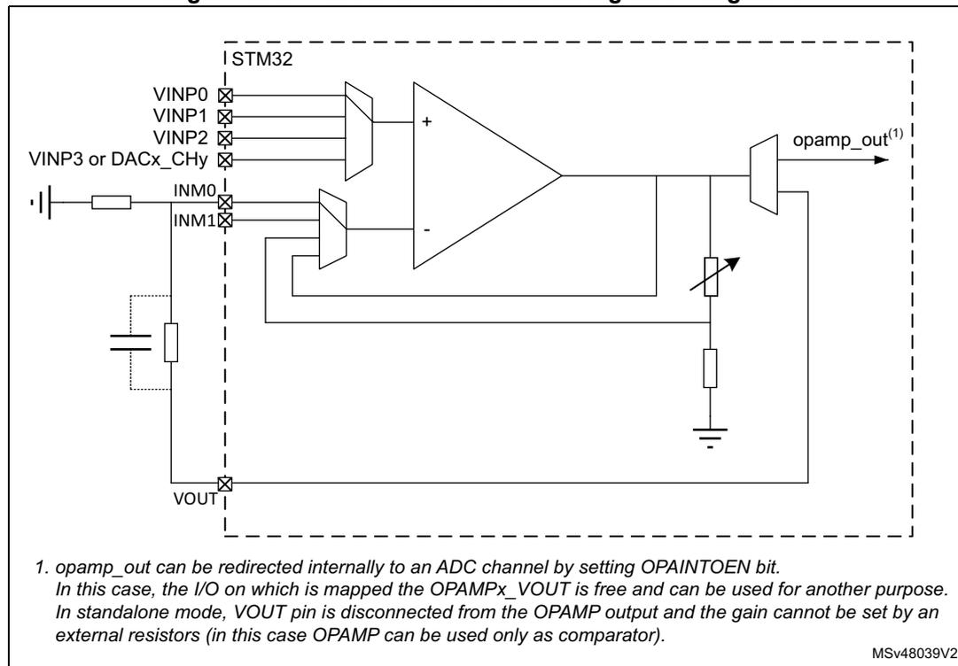
1. opamp_out can be redirected internally to an ADC channel by setting OPAINTOEN bit. In this case, the I/O on which is mapped the OPAMPx_VOUT is free and can be used for another purpose. In standalone mode, VOUT pin is disconnected from the OPAMP output and the gain cannot be set by an external resistors (in this case OPAMP can be used only as comparator).
MSv48039V2
Follower configuration mode
The procedure to use the OPAMP in follower mode is presented hereafter.
- • configure VM_SEL bits as “opamp_out connected to OPAMPx_VINM input”, 11
- • configure VP_SEL bits as “GPIO connected to OPAMPx_VINP”, 00
- • As soon as the OPAEN bit is set, the voltage on pin OPAMPx_VINP is buffered to pin OPAMPx_VOUT.
Note: The pin corresponding to OPAMPx_VINM is free for another usage.
The signal on the OPAMP output is also seen as an ADC input. As a consequence, the OPAMP configured in follower mode can be used to perform impedance adaptation on input signals before feeding them to the ADC input, assuming the input signal frequency is compatible with the operational amplifier gain bandwidth specification.
Figure 172. Follower configuration
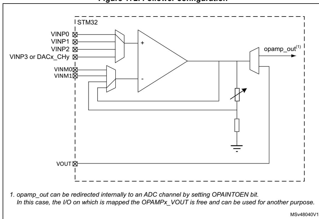
1. opamp_out can be redirected internally to an ADC channel by setting OPAINTOEN bit.
In this case, the I/O on which is mapped the OPAMPx_VOUT is free and can be used for another purpose.
MSv48040V1
Programmable gain amplifier mode
The procedure to use the OPAMP as programmable gain amplifier is presented hereafter.
- • configure VM_SEL bits as “Feedback resistor is connected to OPAMPx_VINM input”, 10
- • configure PGA_GAIN bits as “internal Gain 2, 4, 8, 16, 32, or 64”, 00000 to 00101
- • configure VP_SEL bits as “GPIO connected to OPAMPx_VINP”, 00
As soon as the OPAEN bit is set, the voltage on pin OPAMPx_VINP is amplified by the selected gain and visible on pin OPAMPx_VOUT.
Note: To avoid saturation, the input voltage must stay below \( V_{DDA} \) divided by the selected gain.
Figure 173. PGA mode, internal gain setting (x2/x4/x8/x16/x32/x64), inverting input not used
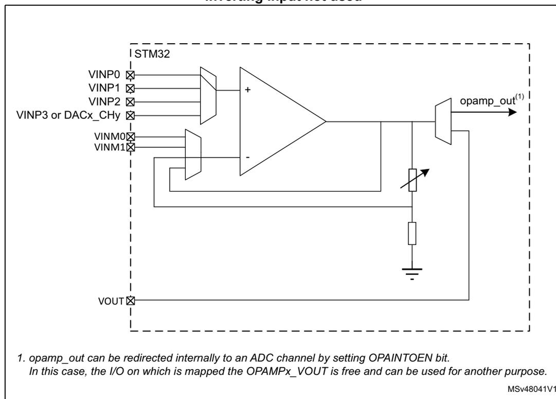
1. opamp_out can be redirected internally to an ADC channel by setting OPAINTOEN bit.
In this case, the I/O on which is mapped the OPAMPx_VOUT is free and can be used for another purpose.
MSv48041V1
Programmable gain amplifier mode with external filtering
The procedure to use the OPAMP to amplify the amplitude of an input signal, with an external filtering, is presented hereafter.
- • configure VM_SEL bits as “Feedback resistor is connected to OPAMPx_VINM input”, 10
- • configure PGA_GAIN bits as “internal Gain 2, 4, 8, 16, 32 or 64 with filtering on VINM0”, 10000 to 10101
- • configure VP_SEL bits as “GPIO connected to OPAMPx_VINP”.
Any external connection on VINM can be used in parallel with the internal PGA, for example a capacitor can be connected between opamp_out and VINM for filtering purpose (see datasheet for the value of resistors used in the PGA resistor network).
Figure 174. PGA mode, internal gain setting (x2/x4/x8/x16/x32/x64), inverting input used for filtering
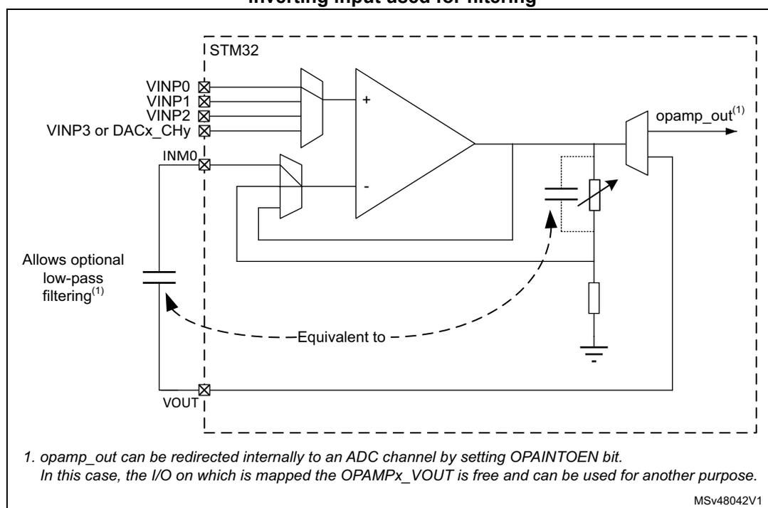
STM32
VINP0
VINP1
VINP2
VINP3 or DACx_CHy
INM0
Allows optional low-pass filtering (1)
Equivalent to
opamp_out (1)
VOUT
1. opamp_out can be redirected internally to an ADC channel by setting OPAINTOEN bit. In this case, the I/O on which is mapped the OPAMPx_VOUT is free and can be used for another purpose.
MSv48042V1
- 1. The gain depends on the cut-off frequency.
Programmable gain amplifier, non-inverting with external bias or inverting mode
The procedure to use the OPAMP to amplify the amplitude of an input signal with bias voltage for non-inverting mode or inverting mode.
- • configure VM_SEL bits as “Feedback resistor is connected to OPAMPx_VINM input”, 10
- • configure PGA_GAIN bits as “Inverting gain = -1, -3, -7, -15, -31, -63 / Non-inverting gain = 2, 4, 8, 16, 32, 64 with VINM0”, 01000 to 01101
- • configure VP_SEL bits as “GPIO connected to OPAMPx_VINP”.
Figure 175. PGA mode, non-inverting gain setting (x2/x4/x8/x16/x32/x64) or inverting gain setting (x-1/x-3/x-7/x-15/x-31/x-63)
1. opamp_out can be redirected internally to an ADC channel by setting OPAINTOEN bit. In this case, the I/O on which is mapped the OPAMPx_VOUT is free and can be used for another purpose.
MSv48043V1
Programmable gain amplifier, non-inverting with external bias or inverting mode with filtering
The procedure to use the OPAMP to amplify the amplitude of an input signal with bias voltage for non-inverting mode or inverting mode with filtering
- • configure VM_SEL bits as “Feedback resistor is connected to OPAMPx_VINM input”, 10
- • configure PGA_GAIN bits as “Inverting gain = -1, -3, -7, -15, -31, -63 / Non-inverting gain = 2, 4, 8, 16, 32, 64 with VINM0, VINM1 pin for filtering”, 11000 to 11101
- • configure VP_SEL bits as “GPIO connected to OPAMPx_VINP”.
Any external connection on VINM1 can be used in parallel with the internal PGA, for example a capacitor can be connected between opamp_out and VINM1 for filtering purpose (see datasheet for the value of resistors used in the PGA resistor network).
Figure 176. PGA mode, non-inverting gain setting (x2/x4/x8/x16/x32/x64) or inverting gain setting (x-1/x-3/x-7/x-15/x-31/x-63) with filtering
1. opamp_out can be redirected internally to an ADC channel by setting OPAINTOEN bit. In this case, the I/O on which is mapped the OPAMPx_VOUT is free and can be used for another purpose.
MSV48045V1
Figure 177. Example configuration
MSV48044V1
25.3.6 OPAMP PGA gain
When the OPAMP is configured in PGA mode, the gain can be programmed to x2, x4, x8, x16, x32, x64 in non-inverting configuration and x-1, x-3, x-7, x-15, x-31, x-63 for inverting configuration.
When the OPAMP is configured in non-inverting mode, the gain solely depends on internal resistive divider. When it is configured as inverting mode, Gain factor is defined not only on the on chip feedback resistor but also the signal source output impedance. If signal source output impedance is not negligible compared to the input feedback resistance of PGA, it creates the gain error.
25.3.7 Calibration
The OPAMP offset value is minimized using a trimming circuitry. At startup, the trimming values are initialized with the preset 'factory' trimming value. Each operational amplifier can also be trimmed by the user if the OPAMP is used in conditions different from the factory trimming conditions.
Each operational amplifier can be trimmed by the user. Specific registers allow to have different trimming values for normal mode and for high-speed mode.
The aim of the calibration is to cancel as much as possible the OPAMP inputs offset voltage. The calibration circuitry allows to reduce the input offset voltage to less than \( \pm 3 \) mV within stable voltage and temperature conditions.
For each operational amplifier and two trimming values (TRIMOFFSETN and TRIMOFFSETP in OPAMPx_CSR register) need to be trimmed, one for N differential pair and one for P differential pair.
The user is able to switch from 'factory' values to 'user' trimmed values using the USERTRIM bit in the OPAMPx_CSR register. This bit is reset at startup and so the 'factory' value are applied by default to the OPAMP option registers.
The offset trimming TRIMOFFSETN and TRIMOFFSETP bits are typically configured after the calibration operation is initialized by setting bit CALON to 1. When CALON = 1 the inputs of the operational amplifier are disconnected from the I/Os.
- • Setting CALSEL to 01 initializes the offset calibration for the P differential pair (low voltage reference used).
- • Resetting CALSEL to 11 initializes the offset calibration for the N differential pair (high voltage reference used).
When CALON = 1, the bit CALOUT reflects the influence of the trimming value selected by CALSEL and OPAHSM. The software must increment the TRIMOFFSETN bits in the OPAMP control register from 0x00 to the first value that causes the CALOUT bit to change from 1 to 0 in the OPAMP register. If the CALOUT bit is reset, the offset is calibrated correctly and the corresponding trimming value must be stored. The CALOUT flag needs up to 2 ms after the trimming value is changed to become steady (see \( t_{OFFTRIMmax} \) delay specification in the electrical characteristics section of the datasheet).
Note: The closer the trimming value is to the optimum trimming value, the longer it takes to stabilize (with a maximum stabilization time remaining below 2 ms in any case).
Table 205. Operating modes and calibration
| Mode | Control bits | Output | ||||
|---|---|---|---|---|---|---|
| OPAEN | OPAHSM | CALON | CALSEL | V OUT | CALOUT flag | |
| Normal operating mode | 1 | 0 | 0 | X | analog | 0 |
| High-speed mode | 1 | 1 | 0 | X | analog | 0 |
| Power down | 0 | X | X | X | Z | 0 |
| Offset cal N | 1 | X | 1 | 11 | analog | X |
| Offset cal P diff | 1 | X | 1 | 01 | analog | X |
Calibration procedure
Here are the steps to perform a full calibration of either one of the operational amplifiers:
- 1. Set the OPAEN bit in OPAMPx_CSR to 1 to enable the operational amplifier.
- 2. Set the USERTRIM bit in the OPAMPx_CSR register to 1.
- 3. Choose a calibration mode (refer to Table 205: Operating modes and calibration ). The steps 3 to 4 have to be repeated four times. For the first iteration select Normal mode and N differential pair. This calibration mode correspond to OPAHSM = 0 and CALSEL = 11 in the OPAMPx_CSR register.
- 4. Increment TRIMOFFSETN[4:0] in OPAMPx_OTR starting from 0b00000 until CALOUT changes to 0 in OPAMPx_CSR.
Note: Between the write to the TRIMOFFSETN bits and the read of the CALOUT value, make sure to wait for the \( t_{OFFTRIMmax} \) delay specified in the electrical characteristics section of the datasheet, to get the correct CALOUT value.
The commutation means that the is correctly compensated and that the corresponding trim code must be saved in the TRIMOFFSETN bits.
Repeat steps 3 to 4 for:
- • Normal mode and P differential pair, CALSEL = 01
- • High-speed mode and N differential pair
- • High-speed mode and P differential pair
If a mode is not used, it is not necessary to perform the corresponding calibration.
All operational amplifier can be calibrated at the same time.
Note: During the whole calibration phase the external connection of the operational amplifier output must not pull up or down currents higher than 500 \( \mu \) A.
If the OPAMP output is internally connected to an ADC channel and disconnected from the output pin (OPAINTOEN = 1 in the OPAMPx_CSR register), the offset trimming procedure differs from the case where the OPAMP output is connected to the output pin (OPAINTOEN = 0). The calibration procedure is the similar as above but the CALOUT bit change detection cannot be used as indicated in step 4. Instead, the ADC output data must be used as indicator to detect the OPAMP output change: a change of CALOUT from 1 to 0 corresponds to the change of ADC output data from values close to the maximum ADC output to values close to the minimum ADC output (the ADC works as a comparator connected to the OPAMP output). Another solution is to perform the calibration with OPAINTOEN = 0, and then change OPAINTOEN to 1. In this case, the OPAMP output GPIO toggles during the calibration and care must be taken that there is no conflict on this GPIO.
25.3.8 Timer controlled Multiplexer mode
The selection of the OPAMP inverting and non inverting inputs can be done automatically. In this case, the switch from one input to another is done automatically. This automatic switch is triggered by the TIM1 CC6 or TIM8 CC6 or TIM20 CC6 output arriving on the OPAMP input multiplexers.
This is useful for dual motor control with a need to measure the currents on the 3 phases simultaneously on a first motor and then on the second motor.
The automatic switch is enabled by setting the TxCMEN bit, x = 1,8,20, in the OPAMP switch control register. The inverting and non inverting inputs selection is performed using
the VPS_SEL and VMS_SEL bit fields in the OPAMP timer controlled mode register. If the TxCMEN bit is cleared, the selection is done using the VP_SEL and VM_SEL bit fields in the OPAMP control/status register.
Figure 178. Timer controlled Multiplexer mode
The diagram illustrates the timing for the timer-controlled multiplexer mode. It shows the following signals and their relationship to the OPAMP input selection:
- CCR6 : Control register for the timer.
- T1 counter : Counter 1 signal.
- T8 counter : Counter 8 signal.
- ADC sampling points : Points where the ADC samples the OPAMP input.
- T1 output (1 out of 3) : Output signal from Counter 1.
- T8 output (1 out of 3) : Output signal from Counter 8.
- T1 CC6 output arriving on OPAMP input mux : Capture/Compare 6 output from Counter 1 that controls the multiplexer.
- OPAMP input selection : The selection between 'Sec' (secondary) and 'Def' (default) inputs based on the T1 CC6 output.
Legend for OPAMP input selection:
Def = default OPAMP input selection
Sec = secondary OPAMP input selection
MS192230V3
25.4 OPAMP low-power modes
Table 206. Effect of low-power modes on the OPAMP
| Mode | Description |
|---|---|
| Sleep | No effect. |
| Low-power run | No effect. |
| Low-power sleep | No effect. |
| Stop 0 / Stop 1 | No effect, OPAMP registers content is kept. |
| Standby | The OPAMP registers are powered down and must be re-initialized after exiting Standby or Shutdown mode. |
| Shutdown |
25.5 OPAMP registers
25.5.1 OPAMP1 control/status register (OPAMP1_CSR)
Address offset: 0x00
Reset value: 0x0000 0000
| 31 | 30 | 29 | 28 | 27 | 26 | 25 | 24 | 23 | 22 | 21 | 20 | 19 | 18 | 17 | 16 |
|---|---|---|---|---|---|---|---|---|---|---|---|---|---|---|---|
| LOCK | CAL OUT | Res. | TRIMOFFSETN[4:0] | TRIMOFFSETP[4:0] | PGA_GAIN[4:2] | ||||||||||
| rw | r | rw | rw | rw | rw | rw | rw | rw | rw | rw | rw | rw | rw | rw | |
| 15 | 14 | 13 | 12 | 11 | 10 | 9 | 8 | 7 | 6 | 5 | 4 | 3 | 2 | 1 | 0 |
|---|---|---|---|---|---|---|---|---|---|---|---|---|---|---|---|
| PGA_GAIN[1:0] | CALSEL[1:0] | CALON | Res. | Res. | OPA INTOEN | OPA HSM | VM_SEL[1:0] | USER TRIM | VP_SEL[1:0] | FORCE VP | OPAEN | ||||
| rw | rw | rw | rw | rw | rw | rw | rw | rw | rw | rw | rw | rw | rw | ||
Bit 31 LOCK : OPAMP1_CSR lock
This bit is write-once. It is set by software. It can only be cleared by a system reset.
This bit is used to configure the OPAMP1_CSR register as read-only.
0: OPAMP1_CSR is read-write
1: OPAMP1_CSR is read-only
Bit 30 CALOUT : Operational amplifier calibration output
This bit shows the digital value of OPAMP output and is the calibration output status during calibration offset mode (Calibration is successful when CALOUT switches from 1 to 0.)
Bit 29 Reserved, must be kept at reset value.
Bits 28:24 TRIMOFFSETN[4:0] : Trim for NMOS differential pairs
Bits 23:19 TRIMOFFSETP[4:0] : Trim for PMOS differential pairs
At reset these bits are loaded by the factory trimming value. They can be modified only when USER_TRIM = 1
Bits 18:14 PGA_GAIN[4:0] : Operational amplifier Programmable amplifier gain value
00000: Non inverting internal gain =2
00001: Non inverting internal gain =4
00010: Non inverting internal gain =8
00011: Non inverting internal gain =16
00100: Non inverting internal gain =32
00101: Non inverting internal gain =64
00110: Not used
00111: Not used
01000: Inverting gain = -1 / non inverting gain =2 with VINM0 pin for input or bias
01001: Inverting gain = -3 / non inverting gain =4 with VINM0 pin for input or bias
01010: Inverting gain = -7 / non inverting gain =8 with VINM0 pin for input or bias
01011: Inverting gain = -15/ non inverting gain =16 VINM0 pin for input or bias
01100: Inverting gain = -31/ non inverting gain =32 VINM0 pin for input or bias
01101: Inverting gain = -63/ non inverting gain =64 VINM0 pin for input or bias
01110: Not used
01111: Not used
10000: Non inverting gain =2 with filtering on VINM0 pin
10001: Non inverting gain =4 with filtering on VINM0 pin
10010: Non inverting gain =8 with filtering on VINM0 pin
10011: Non inverting gain =16 with filtering on VINM0 pin
10100: Non inverting gain =32 with filtering on VINM0 pin
10101: Non inverting gain =64 with filtering on VINM0 pin
10110: Not used
10111: Not used
11000: Inverting gain = -1 / non inverting gain =2 with VINM0 pin for input or bias, VINM1 pin for filtering
11001: Inverting gain = -3 / non inverting gain =4 with VINM0 pin for input or bias, VINM1 pin for filtering
11010: Inverting gain = -7 / non inverting gain =8 with VINM0 pin for input or bias, VINM1 pin for filtering
11011: Inverting gain = -15/ non inverting gain =16 with VINM0 pin for input or bias, VINM1 pin for filtering
11100: Inverting gain = -31/ non inverting gain =32 with VINM0 pin for input or bias, VINM1 pin for filtering
11101: Inverting gain = -63/ non inverting gain =64 with VINM0 pin for input or bias, VINM1 pin for filtering
11110: Not used
11111: Not used
Bits 13:12 CALSEL[1:0] : Calibration selection
It is used to select the offset calibration bus used to generate the internal reference voltage when CALON = 1 or FORCE_VP= 1.
00: 0.033*VDDA applied on OPAMP inputs
01: 0.1*VDDA applied on OPAMP inputs (for PMOS calibration)
10: 0.5*VDDA applied on OPAMP inputs
11: 0.9*VDDA applied on OPAMP inputs (for NMOS calibration)
Bit 11 CALON : Calibration mode enabled
0: Normal mode
1: Calibration mode (all switches opened by HW)
Bits 10:9 Reserved, must be kept at reset value.
Bit 8 OPAINTOEN : Operational amplifier internal output enable.
0: The OPAMP output is connected to the output pin
1: The OPAMP output is connected internally to an ADC channel and disconnected from the output pin
Bit 7 OPAHSM : Operational amplifier high-speed mode
The operational amplifier must be disabled to change this configuration.
0: Operational amplifier in normal mode
1: Operational amplifier in high-speed mode
Bits 6:5 VM_SEL[1:0] : Inverting input selection
00: VINM0 pin connected to OPAMP VINM input
01: VINM1 pin connected to OPAMP VINM input
10: Feedback resistor is connected to OPAMP VINM input (PGA mode), Inverting input selection depends on the PGA_GAIN setting
11: opamp_out connected to OPAMP VINM input (Follower mode)
Bit 4 USERTRIM : User trimming enable
This bit allows to switch from 'factory' AOP offset trimmed values to 'user' AOP offset trimmed values
This bit is active for both mode normal and high-power.
0: 'factory' trim code used
1: 'user' trim code used
Bits 3:2 VP_SEL[1:0] : Non inverted input selection
00: VINP0 pin connected to OPAMP1 VINP input
01: VINP1 pin connected to OPAMP1 VINP input
10: VINP2 pin connected to OPAMP1 VINP input
11: DAC3_CH1 connected to OPAMP1 VINP input
Bit 1 FORCE_VP : Force internal reference on OPAMP VINP input (reserved for test)
0: Normal operating mode. Non-inverting input connected to inputs.
1: Calibration verification mode: Non-inverting input connected to calibration reference voltage.
Bit 0 OPAEN : Operational amplifier Enable
0: Operational amplifier disabled
1: Operational amplifier enabled
25.5.2 OPAMP2 control/status register (OPAMP2_CSR)
Address offset: 0x04
Reset value: 0x0000 0000
| 31 | 30 | 29 | 28 | 27 | 26 | 25 | 24 | 23 | 22 | 21 | 20 | 19 | 18 | 17 | 16 |
|---|---|---|---|---|---|---|---|---|---|---|---|---|---|---|---|
| LOCK | CAL OUT | Res. | TRIMOFFSETN[4:0] | TRIMOFFSETP[4:0] | PGA_GAIN[4:2] | ||||||||||
| rw | r | rw | rw | rw | rw | rw | rw | rw | rw | rw | rw | rw | rw | rw | |
| 15 | 14 | 13 | 12 | 11 | 10 | 9 | 8 | 7 | 6 | 5 | 4 | 3 | 2 | 1 | 0 |
|---|---|---|---|---|---|---|---|---|---|---|---|---|---|---|---|
| PGA_GAIN[1:0] | CALSEL[1:0] | CALON | Res. | Res. | OPA INTOEN | OPA HSM | VM_SEL[1:0] | USER TRIM | VP_SEL[1:0] | FORCE VP | OPAEN | ||||
| rw | rw | rw | rw | rw | rw | rw | rw | rw | rw | rw | rw | rw | rw | ||
Bit 31 LOCK : OPAMP2_CSR lock
This bit is write-once. It is set by software. It can only be cleared by a system reset.
This bit is used to configure the OPAMP2_CSR register as read-only.
0: OPAMP2_CSR is read-write
1: OPAMP2_CSR is read-only
Bit 30 CALOUT : Operational amplifier calibration output
This bit shows the digital value of OPAMP output and is the calibration output status during calibration offset mode (Calibration is successful when CALOUT switches from 1 to 0.)
Bit 29 Reserved, must be kept at reset value.
Bits 28:24 TRIMOFFSETN[4:0] : Trim for NMOS differential pairs
Bits 23:19 TRIMOFFSETP[4:0] : Trim for PMOS differential pairs
At reset these bits are loaded by the factory trimming value. They can be modified only when USER_TRIM = 1
Bits 18:14 PGA_GAIN[4:0] : Operational amplifier Programmable amplifier gain value
00000: Non inverting internal gain =2
00001: Non inverting internal gain =4
00010: Non inverting internal gain =8
00011: Non inverting internal gain =16
00100: Non inverting internal gain =32
00101: Non inverting internal gain =64
00110: Not used
00111: Not used
01000: Inverting gain = -1 / non inverting gain =2 with VINM0 pin for input or bias
01001: Inverting gain = -3 / non inverting gain =4 with VINM0 pin for input or bias
01010: Inverting gain = -7 / non inverting gain =8 with VINM0 pin for input or bias
01011: Inverting gain = -15/ non inverting gain =16 VINM0 pin for input or bias
01100: Inverting gain = -31/ non inverting gain =32 VINM0 pin for input or bias
01101: Inverting gain = -63/ non inverting gain =64 VINM0 pin for input or bias
01110: Not used
01111: Not used
10000: Non inverting gain =2 with filtering on VINM0 pin
10001: Non inverting gain =4 with filtering on VINM0 pin
10010: Non inverting gain =8 with filtering on VINM0 pin
10011: Non inverting gain =16 with filtering on VINM0 pin
10100: Non inverting gain =32 with filtering on VINM0 pin
10101: Non inverting gain =64 with filtering on VINM0 pin
10110: Not used
10111: Not used
11000: Inverting gain = -1 / non inverting gain =2 with VINM0 pin for input or bias, VINM1 pin for filtering
11001: Inverting gain = -3 / non inverting gain =4 with VINM0 pin for input or bias, VINM1 pin for filtering
11010: Inverting gain = -7 / non inverting gain =8 with VINM0 pin for input or bias, VINM1 pin for filtering
11011: Inverting gain = -15/ non inverting gain =16 with VINM0 pin for input or bias, VINM1 pin for filtering
11100: Inverting gain = -31/ non inverting gain =32 with VINM0 pin for input or bias, VINM1 pin for filtering
11101: Inverting gain = -63/ non inverting gain =64 with VINM0 pin for input or bias, VINM1 pin for filtering
11110: Not used
11111: Not used
Bits 13:12 CALSEL[1:0] : Calibration selection
It is used to select the offset calibration bus used to generate the internal reference voltage when CALON = 1 or FORCE_VP= 1.
00: 0.033*VDDA applied on OPAMP inputs
01: 0.1*VDDA applied on OPAMP inputs (for PMOS calibration)
10: 0.5*VDDA applied on OPAMP inputs
11: 0.9*VDDA applied on OPAMP inputs (for NMOS calibration)
Bit 11 CALON : Calibration mode enabled
0: Normal mode
1: Calibration mode (all switches opened by HW)
Bits 10:9 Reserved, must be kept at reset value.
Bit 8 OPAINTOEN : Operational amplifier internal output enable.
0: The OPAMP output is connected to the output pin
1: The OPAMP output is connected internally to an ADC channel and disconnected from the output pin
Bit 7 OPAHSM : Operational amplifier high-speed mode
The operational amplifier must be disabled to change this configuration.
0: Operational amplifier in normal mode
1: Operational amplifier in high-speed mode
Bits 6:5 VM_SEL[1:0] : Inverting input selection
00: VINM0 pin connected to OPAMP VINM input
01: VINM1 pin connected to OPAMP VINM input
10: Feedback resistor is connected to OPAMP VINM input (PGA mode), Inverting input selection depends on the PGA_GAIN setting
11: opamp_out connected to OPAMP VINM input (Follower mode)
Bit 4 USERTRIM : User trimming enable
This bit allows to switch from 'factory' AOP offset trimmed values to 'user' AOP offset trimmed values
This bit is active for both mode normal and high-power.
0: 'factory' trim code used
1: 'user' trim code used
Bits 3:2 VP_SEL[1:0] : Non inverted input selection
00: VINP0 pin connected to OPAMP2 VINP input
01: VINP1 pin connected to OPAMP2 VINP input
10: VINP2 pin connected to OPAMP2 VINP input
11: VINP3 pin connected to OPAMP2 VINP input
Bit 1 FORCE_VP : Force internal reference on VP (reserved for test)
0: Normal operating mode. Non-inverting input connected to inputs.
1: Calibration verification mode: Non-inverting input connected to calibration reference voltage.
Bit 0 OPAEN : Operational amplifier Enable
0: Operational amplifier disabled
1: Operational amplifier enabled
25.5.3 OPAMP3 control/status register (OPAMP3_CSR)
Address offset: 0x08
Reset value: 0x0000 0000
| 31 | 30 | 29 | 28 | 27 | 26 | 25 | 24 | 23 | 22 | 21 | 20 | 19 | 18 | 17 | 16 |
|---|---|---|---|---|---|---|---|---|---|---|---|---|---|---|---|
| LOCK | CALOUT | Res. | TRIMOFFSETN[4:0] | TRIMOFFSETP[4:0] | PGA_GAIN[4:2] | ||||||||||
| rw | r | rw | rw | rw | rw | rw | rw | rw | rw | rw | rw | rw | rw | rw | |
| 15 | 14 | 13 | 12 | 11 | 10 | 9 | 8 | 7 | 6 | 5 | 4 | 3 | 2 | 1 | 0 |
|---|---|---|---|---|---|---|---|---|---|---|---|---|---|---|---|
| PGA_GAIN[1:0] | CALSEL[1:0] | CALON | Res. | Res. | OPA INTOEN | OPA HSM | VM_SEL[1:0] | USER TRIM | VP_SEL[1:0] | FORCE _VP | OPAEN | ||||
| rw | rw | rw | rw | rw | rw | rw | rw | rw | rw | rw | rw | rw | rw | ||
Bit 31 LOCK : OPAMP3_CSR lock
This bit is write-once. It is set by software. It can only be cleared by a system reset.
This bit is used to configure the OPAMP3_CSR register as read-only.
- 0: OPAMP3_CSR is read-write
- 1: OPAMP3_CSR is read-only
Bit 30 CALOUT : Operational amplifier calibration output
This bit shows the digital value of OPAMP output and is the calibration output status during calibration offset mode (Calibration is successful when CALOUT switches from 1 to 0.)
Bit 29 Reserved, must be kept at reset value.
Bits 28:24 TRIMOFFSETN[4:0] : Trim for NMOS differential pairs
Bits 23:19 TRIMOFFSETP[4:0] : Trim for PMOS differential pairs
At reset these bits are loaded by the factory trimming value. They can be modified only when USER_TRIM = 1
Bits 18:14 PGA_GAIN[4:0] : Operational amplifier Programmable amplifier gain value
00000: Non inverting internal gain =2
00001: Non inverting internal gain =4
00010: Non inverting internal gain =8
00011: Non inverting internal gain =16
00100: Non inverting internal gain =32
00101: Non inverting internal gain =64
00110: Not used
00111: Not used
01000: Inverting gain = -1 / non inverting gain =2 with VINM0 pin for input or bias
01001: Inverting gain = -3 / non inverting gain =4 with VINM0 pin for input or bias
01010: Inverting gain = -7 / non inverting gain =8 with VINM0 pin for input or bias
01011: Inverting gain = -15/ non inverting gain =16 VINM0 pin for input or bias
01100: Inverting gain = -31/ non inverting gain =32 VINM0 pin for input or bias
01101: Inverting gain = -63/ non inverting gain =64 VINM0 pin for input or bias
01110: Not used
01111: Not used
10000: Non inverting gain =2 with filtering on VINM0 pin
10001: Non inverting gain =4 with filtering on VINM0 pin
10010: Non inverting gain =8 with filtering on VINM0 pin
10011: Non inverting gain =16 with filtering on VINM0 pin
10100: Non inverting gain =32 with filtering on VINM0 pin
10101: Non inverting gain =64 with filtering on VINM0 pin
10110: Not used
10111: Not used
11000: Inverting gain = -1 / non inverting gain =2 with VINM0 pin for input or bias, VINM1 pin for filtering
11001: Inverting gain = -3 / non inverting gain =4 with VINM0 pin for input or bias, VINM1 pin for filtering
11010: Inverting gain = -7 / non inverting gain =8 with VINM0 pin for input or bias, VINM1 pin for filtering
11011: Inverting gain = -15/ non inverting gain =16 with VINM0 pin for input or bias, VINM1 pin for filtering
11100: Inverting gain = -31/ non inverting gain =32 with VINM0 pin for input or bias, VINM1 pin for filtering
11101: Inverting gain = -63/ non inverting gain =64 with VINM0 pin for input or bias, VINM1 pin for filtering
11110: Not used
11111: Not used
Bits 13:12 CALSEL[1:0] : Calibration selection
It is used to select the offset calibration bus used to generate the internal reference voltage when CALON = 1 or FORCE_VP= 1.
00: 0.033*VDDA applied on OPAMP inputs
01: 0.1*VDDA applied on OPAMP inputs (for PMOS calibration)
10: 0.5*VDDA applied on OPAMP inputs
11: 0.9*VDDA applied on OPAMP inputs (for NMOS calibration)
Bit 11 CALON : Calibration mode enabled
0: Normal mode
1: Calibration mode (all switches opened by HW)
Bits 10:9 Reserved, must be kept at reset value.
Bit 8 OPAINTOEN : Operational amplifier internal output enable.
0: The OPAMP output is connected to the output pin
1: The OPAMP output is connected internally to an ADC channel and disconnected from the output pin
Bit 7 OPAHSM : Operational amplifier high-speed mode
The operational amplifier must be disable to change this configuration.
0: Operational amplifier in normal mode
1: Operational amplifier in high-speed mode
Bits 6:5 VM_SEL[1:0] : Inverting input selection
00: VINM0 pin connected to OPAMP VINM input
01: VINM1 pin connected to OPAMP VINM input
10: Feedback resistor is connected to OPAMP VINM input (PGA mode), Inverting input selection is depends on the PGA_GAIN setting
11: opamp_out connected to OPAMP VINM input (Follower mode)
Bit 4 USERTRIM : User trimming enable
This bit allows to switch from 'factory' AOP offset trimmed values to 'user' AOP offset trimmed values
This bit is active for both mode normal and high-power.
0: 'factory' trim code used
1: 'user' trim code used
Bits 3:2 VP_SEL[1:0] : Non inverted input selection
00: VINP0 pin connected to OPAMP3 VINP input
01: VINP1 pin connected to OPAMP3 VINP input
10: VINP2 pin connected to OPAMP3 VINP input
11: DAC3_CH2 connected to OPAMP3 VINP input
Bit 1 FORCE_VP : Force internal reference on VP (reserved for test)
0: Normal operating mode. Non-inverting input connected to inputs.
1: Calibration verification mode: Non-inverting input connected to calibration reference voltage.
Bit 0 OPAEN : Operational amplifier Enable
0: Operational amplifier disabled
1: Operational amplifier enabled
25.5.4 OPAMP4 control/status register (OPAMP4_CSR)
Address offset: 0x0C
Reset value: 0x0000 0000
| 31 | 30 | 29 | 28 | 27 | 26 | 25 | 24 | 23 | 22 | 21 | 20 | 19 | 18 | 17 | 16 |
|---|---|---|---|---|---|---|---|---|---|---|---|---|---|---|---|
| LOCK | CAL OUT | Res. | TRIMOFFSETN[4:0] | TRIMOFFSETP[4:0] | PGA_GAIN[4:2] | ||||||||||
| rw | r | rw | rw | rw | rw | rw | rw | rw | rw | rw | rw | rw | rw | rw | |
| 15 | 14 | 13 | 12 | 11 | 10 | 9 | 8 | 7 | 6 | 5 | 4 | 3 | 2 | 1 | 0 |
|---|---|---|---|---|---|---|---|---|---|---|---|---|---|---|---|
| PGA_GAIN[1:0] | CALSEL[1:0] | CALON | Res. | Res. | OPA INTOEN | OPA HSM | VM_SEL[1:0] | USER TRIM | VP_SEL[1:0] | FORCE VP | OPAEN | ||||
| rw | rw | rw | rw | rw | rw | rw | rw | rw | rw | rw | rw | rw | rw | ||
Bit 31 LOCK : OPAMP4_CSR lock
This bit is write-once. It is set by software. It can only be cleared by a system reset.
This bit is used to configure the OPAMP4_CSR register as read-only.
0: OPAMP4_CSR is read-write
1: OPAMP4_CSR is read-only
Bit 30 CALOUT : Operational amplifier calibration output
This bit shows the digital value of OPAMP output and is the calibration output status during calibration offset mode (Calibration is successful when CALOUT switches from 1 to 0.)
Bit 29 Reserved, must be kept at reset value.
Bits 28:24 TRIMOFFSETN[4:0] : Trim for NMOS differential pairs
Bits 23:19 TRIMOFFSETP[4:0] : Trim for PMOS differential pairs
At reset these bits are loaded by the factory trimming value. They can be modified only when USER_TRIM = 1
Bits 18:14 PGA_GAIN[4:0] : Operational amplifier Programmable amplifier gain value
00000: Non inverting internal gain =2
00001: Non inverting internal gain =4
00010: Non inverting internal gain =8
00011: Non inverting internal gain =16
00100: Non inverting internal gain =32
00101: Non inverting internal gain =64
00110: Not used
00111: Not used
01000: Inverting gain = -1 / non inverting gain =2 with VINM0 pin for input or bias
01001: Inverting gain = -3 / non inverting gain =4 with VINM0 pin for input or bias
01010: Inverting gain = -7 / non inverting gain =8 with VINM0 pin for input or bias
01011: Inverting gain = -15/ non inverting gain =16 VINM0 pin for input or bias
01100: Inverting gain = -31/ non inverting gain =32 VINM0 pin for input or bias
01101: Inverting gain = -63/ non inverting gain =64 VINM0 pin for input or bias
01110: Not used
01111: Not used
10000: Non inverting gain =2 with filtering on VINM0 pin
10001: Non inverting gain =4 with filtering on VINM0 pin
10010: Non inverting gain =8 with filtering on VINM0 pin
10011: Non inverting gain =16 with filtering on VINM0 pin
10100: Non inverting gain =32 with filtering on VINM0 pin
10101: Non inverting gain =64 with filtering on VINM0 pin
10110: Not used
10111: Not used
11000: Inverting gain = -1 / non inverting gain =2 with VINM0 pin for input or bias, VINM1 pin for filtering
11001: Inverting gain = -3 / non inverting gain =4 with VINM0 pin for input or bias, VINM1 pin for filtering
11010: Inverting gain = -7 / non inverting gain =8 with VINM0 pin for input or bias, VINM1 pin for filtering
11011: Inverting gain = -15/ non inverting gain =16 with VINM0 pin for input or bias, VINM1 pin for filtering
11100: Inverting gain = -31/ non inverting gain =32 with VINM0 pin for input or bias, VINM1 pin for filtering
11101: Inverting gain = -63/ non inverting gain =64 with VINM0 pin for input or bias, VINM1 pin for filtering
11110: Not used
11111: Not used
Bits 13:12 CALSEL[1:0] : Calibration selection
It is used to select the offset calibration bus used to generate the internal reference voltage when CALON = 1 or FORCE_VP= 1.
00: 0.033*VDDA applied on OPAMP inputs
01: 0.1*VDDA applied on OPAMP inputs (for PMOS calibration)
10: 0.5*VDDA applied on OPAMP inputs
11: 0.9*VDDA applied on OPAMP inputs (for NMOS calibration)
Bit 11 CALON : Calibration mode enabled
0: Normal mode
1: Calibration mode (all switches opened by HW)
Bits 10:9 Reserved, must be kept at reset value.
Bit 8 OPAINTOEN : Operational amplifier internal output enable.
0: The OPAMP output is connected to the output pin
1: The OPAMP output is connected internally to an ADC channel and disconnected from the output pin
Bit 7 OPAHSM : Operational amplifier high-speed mode
The operational amplifier must be disabled to change this configuration.
0: Operational amplifier in normal mode
1: Operational amplifier in high-speed mode
Bits 6:5 VM_SEL[1:0] : Inverting input selection
00: VINM0 pin connected to OPAMP VINM input
01: VINM1 pin connected to OPAMP VINM input
10: Feedback resistor is connected to OPAMP VINM input (PGA mode), Inverting input selection depends on the PGA_GAIN setting
11: opamp_out connected to OPAMP VINM input (Follower mode)
Bit 4 USERTRIM : User trimming enable
This bit allows to switch from 'factory' AOP offset trimmed values to 'user' AOP offset trimmed values
This bit is active for both mode normal and high-power.
0: 'factory' trim code used
1: 'user' trim code used
Bits 3:2 VP_SEL[1:0] : Non inverted input selection
00: VINP0 pin connected to OPAMP4 VINP input
01: VINP1 pin connected to OPAMP4 VINP input
10: VINP2 pin connected to OPAMP4 VINP input
11: DAC4_CH1 connected to OPAMP4 VINP input
Bit 1 FORCE_VP : Force internal reference on VP (reserved for test)
0: Normal operating mode. Non-inverting input connected to inputs.
1: Calibration verification mode: Non-inverting input connected to calibration reference voltage.
Bit 0 OPAEN : Operational amplifier Enable
0: Operational amplifier disabled
1: Operational amplifier enabled
25.5.5 OPAMP5 control/status register (OPAMP5_CSR)
Address offset: 0x10
Reset value: 0x0000 0000
| 31 | 30 | 29 | 28 | 27 | 26 | 25 | 24 | 23 | 22 | 21 | 20 | 19 | 18 | 17 | 16 |
|---|---|---|---|---|---|---|---|---|---|---|---|---|---|---|---|
| LOCK | CALOUT | Res. | TRIMOFFSETN[4:0] | TRIMOFFSETP[4:0] | PGA_GAIN[4:2] | ||||||||||
| rw | r | rw | rw | rw | rw | rw | rw | rw | rw | rw | rw | rw | rw | rw | |
| 15 | 14 | 13 | 12 | 11 | 10 | 9 | 8 | 7 | 6 | 5 | 4 | 3 | 2 | 1 | 0 |
|---|---|---|---|---|---|---|---|---|---|---|---|---|---|---|---|
| PGA_GAIN[1:0] | CALSEL[1:0] | CALON | Res. | Res. | OPA INTOEN | OPA HSM | VM_SEL[1:0] | USER TRIM | VP_SEL[1:0] | FORCE VP | OPAEN | ||||
| rw | rw | rw | rw | rw | rw | rw | rw | rw | rw | rw | rw | rw | rw | ||
Bit 31 LOCK : OPAMP5_CSR lock
This bit is write-once. It is set by software. It can only be cleared by a system reset.
This bit is used to configure the OPAMP5_CSR register as read-only.
0: OPAMP5_CSR is read-write
1: OPAMP5_CSR is read-only
Bit 30 CALOUT : Operational amplifier calibration output
This bit shows the digital value of OPAMP output and is the calibration output status during calibration offset mode (Calibration is successful when CALOUT switches from 1 to 0.)
Bit 29 Reserved, must be kept at reset value.
Bits 28:24 TRIMOFFSETN[4:0] : Trim for NMOS differential pairs
Bits 23:19 TRIMOFFSETP[4:0] : Trim for PMOS differential pairs
At reset these bits are loaded by the factory trimming value. They can be modified only when USER_TRIM = 1
Bits 18:14 PGA_GAIN[4:0] : Operational amplifier Programmable amplifier gain value
00000: Non inverting internal gain =2
00001: Non inverting internal gain =4
00010: Non inverting internal gain =8
00011: Non inverting internal gain =16
00100: Non inverting internal gain =32
00101: Non inverting internal gain =64
00110: Not used
00111: Not used
01000: Inverting gain = -1 / non inverting gain =2 with VINM0 pin for input or bias
01001: Inverting gain = -3 / non inverting gain =4 with VINM0 pin for input or bias
01010: Inverting gain = -7 / non inverting gain =8 with VINM0 pin for input or bias
01011: Inverting gain = -15/ non inverting gain =16 VINM0 pin for input or bias
01100: Inverting gain = -31/ non inverting gain =32 VINM0 pin for input or bias
01101: Inverting gain = -63/ non inverting gain =64 VINM0 pin for input or bias
01110: Not used
01111: Not used
10000: Non inverting gain =2 with filtering on VINM0 pin
10001: Non inverting gain =4 with filtering on VINM0 pin
10010: Non inverting gain =8 with filtering on VINM0 pin
10011: Non inverting gain =16 with filtering on VINM0 pin
10100: Non inverting gain =32 with filtering on VINM0 pin
10101: Non inverting gain =64 with filtering on VINM0 pin
10110: Not used
10111: Not used
11000: Inverting gain = -1 / non inverting gain =2 with VINM0 pin for input or bias, VINM1 pin for filtering
11001: Inverting gain = -3 / non inverting gain =4 with VINM0 pin for input or bias, VINM1 pin for filtering
11010: Inverting gain = -7 / non inverting gain =8 with VINM0 pin for input or bias, VINM1 pin for filtering
11011: Inverting gain = -15/ non inverting gain =16 with VINM0 pin for input or bias, VINM1 pin for filtering
11100: Inverting gain = -31/ non inverting gain =32 with VINM0 pin for input or bias, VINM1 pin for filtering
11101: Inverting gain = -63/ non inverting gain =64 with VINM0 pin for input or bias, VINM1 pin for filtering
11110: Not used
11111: Not used
Bits 13:12 CALSEL[1:0] : Calibration selection
It is used to select the offset calibration bus used to generate the internal reference voltage when CALON = 1 or FORCE_VP= 1.
00: 0.033*VDDA applied on OPAMP inputs
01: 0.1*VDDA applied on OPAMP inputs (for PMOS calibration)
10: 0.5*VDDA applied on OPAMP inputs
11: 0.9*VDDA applied on OPAMP inputs (for NMOS calibration)
Bit 11 CALON : Calibration mode enabled
0: Normal mode
1: Calibration mode (all switches opened by HW)
Bits 10:9 Reserved, must be kept at reset value.
Bit 8 OPAINTOEN : Operational amplifier internal output enable.
0: The OPAMP output is connected to the output pin
1: The OPAMP output is connected internally to an ADC channel and disconnected from the output pin
Bit 7 OPAHSM : Operational amplifier high-speed mode
The operational amplifier must be disabled to change this configuration.
0: Operational amplifier in normal mode
1: Operational amplifier in high-speed mode
Bits 6:5 VM_SEL[1:0] : Inverting input selection
00: VINM0 pin connected to OPAMP VINM input
01: VINM1 pin connected to OPAMP VINM input
10: Feedback resistor is connected to OPAMP VINM input (PGA mode), Inverting input selection depends on the PGA_GAIN setting
11: opamp_out connected to OPAMP VINM input (Follower mode)
Bit 4 USERTRIM : User trimming enable
This bit allows to switch from 'factory' AOP offset trimmed values to 'user' AOP offset trimmed values
This bit is active for both mode normal and high-power.
0: 'factory' trim code used
1: 'user' trim code used
Bits 3:2 VP_SEL[1:0] : Non inverted input selection
00: VINP0 pin connected to OPAMP5 VINP input
01: VINP1 pin connected to OPAMP5 VINP input
10: VINP2 pin connected to OPAMP5 VINP input
11: DAC4_CH2 connected to OPAMP5 VINP input
Bit 1 FORCE_VP : Force internal reference on VP (reserved for test)
0: Normal operating mode. Non-inverting input connected to inputs.
1: Calibration verification mode: Non-inverting input connected to calibration reference voltage.
Bit 0 OPAEN : Operational amplifier Enable
0: Operational amplifier disabled
1: Operational amplifier enabled
25.5.6 OPAMP6 control/status register (OPAMP6_CSR)
Address offset: 0x14
Reset value: 0x0000 0000
| 31 | 30 | 29 | 28 | 27 | 26 | 25 | 24 | 23 | 22 | 21 | 20 | 19 | 18 | 17 | 16 |
|---|---|---|---|---|---|---|---|---|---|---|---|---|---|---|---|
| LOCK | CAL OUT | Res. | TRIMOFFSETN[4:0] | TRIMOFFSETTP[4:0] | PGA_GAIN[4:2] | ||||||||||
| rw | r | rw | rw | rw | rw | rw | rw | rw | rw | rw | rw | rw | rw | rw | |
| 15 | 14 | 13 | 12 | 11 | 10 | 9 | 8 | 7 | 6 | 5 | 4 | 3 | 2 | 1 | 0 |
|---|---|---|---|---|---|---|---|---|---|---|---|---|---|---|---|
| PGA_GAIN[1:0] | CALSEL[1:0] | CALON | Res. | Res. | OPA INTOEN | OPA HSM | VM_SEL[1:0] | USER TRIM | VP_SEL[1:0] | FORCE VP | OPAEN | ||||
| rw | rw | rw | rw | rw | rw | rw | rw | rw | rw | rw | rw | rw | rw | ||
Bit 31 LOCK : OPAMP6_CSR lock
This bit is write-once. It is set by software. It can only be cleared by a system reset.
This bit is used to configure the OPAMP6_CSR register as read-only.
0: OPAMP6_CSR is read-write
1: OPAMP6_CSR is read-only
Bit 30 CALOUT : Operational amplifier calibration output
This bit shows the digital value of OPAMP output and is the calibration output status during calibration offset mode (Calibration is successful when CALOUT switches from 1 to 0.)
Bit 29 Reserved, must be kept at reset value.
Bits 28:24 TRIMOFFSETN[4:0] : Trim for NMOS differential pairs
Bits 23:19 TRIMOFFSETTP[4:0] : Trim for PMOS differential pairs
At reset these bits are loaded by the factory trimming value. They can be modified only when USER_TRIM = 1
Bits 18:14 PGA_GAIN[4:0] : Operational amplifier Programmable amplifier gain value
00000: Non inverting internal gain =2
00001: Non inverting internal gain =4
00010: Non inverting internal gain =8
00011: Non inverting internal gain =16
00100: Non inverting internal gain =32
00101: Non inverting internal gain =64
00110: Not used
00111: Not used
01000: Inverting gain = -1 / non inverting gain =2 with VINM0 pin for input or bias
01001: Inverting gain = -3 / non inverting gain =4 with VINM0 pin for input or bias
01010: Inverting gain = -7 / non inverting gain =8 with VINM0 pin for input or bias
01011: Inverting gain = -15/ non inverting gain =16 VINM0 pin for input or bias
01100: Inverting gain = -31/ non inverting gain =32 VINM0 pin for input or bias
01101: Inverting gain = -63/ non inverting gain =64 VINM0 pin for input or bias
01110: Not used
01111: Not used
10000: Non inverting gain =2 with filtering on VINM0 pin
10001: Non inverting gain =4 with filtering on VINM0 pin
10010: Non inverting gain =8 with filtering on VINM0 pin
10011: Non inverting gain =16 with filtering on VINM0 pin
10100: Non inverting gain =32 with filtering on VINM0 pin
10101: Non inverting gain =64 with filtering on VINM0 pin
10110: Not used
10111: Not used
11000: Inverting gain = -1 / non inverting gain =2 with VINM0 pin for input or bias, VINM1 pin for filtering
11001: Inverting gain = -3 / non inverting gain =4 with VINM0 pin for input or bias, VINM1 pin for filtering
11010: Inverting gain = -7 / non inverting gain =8 with VINM0 pin for input or bias, VINM1 pin for filtering
11011: Inverting gain = -15/ non inverting gain =16 with VINM0 pin for input or bias, VINM1 pin for filtering
11100: Inverting gain = -31/ non inverting gain =32 with VINM0 pin for input or bias, VINM1 pin for filtering
11101: Inverting gain = -63/ non inverting gain =64 with VINM0 pin for input or bias, VINM1 pin for filtering
11110: Not used
11111: Not used
Bits 13:12 CALSEL[1:0] : Calibration selection
It is used to select the offset calibration bus used to generate the internal reference voltage when CALON = 1 or FORCE_VP= 1.
00: 0.033*VDDA applied on OPAMP inputs
01: 0.1*VDDA applied on OPAMP inputs (for PMOS calibration)
10: 0.5*VDDA applied on OPAMP inputs
11: 0.9*VDDA applied on OPAMP inputs (for NMOS calibration)
Bit 11 CALON : Calibration mode enabled
0: Normal mode
1: Calibration mode (all switches opened by HW)
Bits 10:9 Reserved, must be kept at reset value.
Bit 8 OPAINTOEN : Operational amplifier internal output enable.
0: The OPAMP output is connected to the output pin
1: The OPAMP output is connected internally to an ADC channel and disconnected from the output pin
Bit 7 OPAHSM : Operational amplifier high-speed mode
The operational amplifier must be disabled to change this configuration.
0: Operational amplifier in normal mode
1: Operational amplifier in high-speed mode
Bits 6:5 VM_SEL[1:0] : Inverting input selection
00: VINM0 pin connected to OPAMP VINM input
01: VINM1 pin connected to OPAMP VINM input
10: Feedback resistor is connected to OPAMP VINM input (PGA mode), Inverting input selection depends on the PGA_GAIN setting
11: opamp_out connected to OPAMP VINM input (Follower mode)
Bit 4 USERTRIM : User trimming enable
This bit allows to switch from 'factory' AOP offset trimmed values to 'user' AOP offset trimmed values
This bit is active for both mode normal and high-power.
0: 'factory' trim code used
1: 'user' trim code used
Bits 3:2 VP_SEL[1:0] : Non inverted input selection
00: VINP0 pin connected to OPAMP6 VINP input
01: VINP1 pin connected to OPAMP6 VINP input
10: VINP2 pin connected to OPAMP6 VINP input
11: DAC3_CH1 connected to OPAMP6 VINP input
Bit 1 FORCE_VP : Force internal reference on VP (reserved for test)
0: Normal operating mode. Non-inverting input connected to inputs.
1: Calibration verification mode: Non-inverting input connected to calibration reference voltage.
Bit 0 OPAEN : Operational amplifier Enable
0: Operational amplifier disabled
1: Operational amplifier enabled
25.5.7 OPAMP1 timer controlled mode register (OPAMPx_TCMR) (x = 1...6)
Address offset: 0x18
Reset value: 0x0000 0000
| 31 | 30 | 29 | 28 | 27 | 26 | 25 | 24 | 23 | 22 | 21 | 20 | 19 | 18 | 17 | 16 |
|---|---|---|---|---|---|---|---|---|---|---|---|---|---|---|---|
| LOCK | Res. | Res. | Res. | Res. | Res. | Res. | Res. | Res. | Res. | Res. | Res. | Res. | Res. | Res. | Res. |
| rw | |||||||||||||||
| 15 | 14 | 13 | 12 | 11 | 10 | 9 | 8 | 7 | 6 | 5 | 4 | 3 | 2 | 1 | 0 |
| Res. | Res. | Res. | Res. | Res. | Res. | Res. | Res. | Res. | Res. | T20CM _EN | T8CM _EN | T1CM _EN | VPS_SEL[1:0] | VMS _SEL | |
| rw | rw | rw | rw | rw | rw |
Bit 31 LOCK: OPAMP1_TCMR lock
This bit is write-once. It is set by software. It can only be cleared by a system reset.
This bit is used to configure the OPAMP1_TCMR register as read-only.
0: OPAMP1_TCMR is read-write
1: OPAMP1_TCMR is read-only
Bits 30:6 Reserved, must be kept at reset value.
Bit 5 T20CM_EN: TIM20 controlled mux mode enable
This bit is set and cleared by software. It is used to control automatically the switch between the default selection (VP_SEL and VM_SEL) and the secondary selection (VPS_SEL and VMS_SEL) of the inverting and non inverting inputs. This automatic switch is triggered by the TIM20 CC6 output arriving on the OPAMPx input multiplexers.
0: Automatic switch is disabled.
1: Automatic switch is enabled.
Bit 4 T8CM_EN: TIM8 controlled mux mode enable
This bit is set and cleared by software. It is used to control automatically the switch between the default selection (VP_SEL and VM_SEL) and the secondary selection (VPS_SEL and VMS_SEL) of the inverting and non inverting inputs. This automatic switch is triggered by the TIM8 CC6 output arriving on the OPAMPx input multiplexers.
0: Automatic switch is disabled.
1: Automatic switch is enabled.
Bit 3 T1CM_EN: TIM1 controlled mux mode enableThis bit is set and cleared by software. It is used to control automatically the switch between the default selection (VP_SEL and VM_SEL) and the secondary selection (VPS_SEL and VMS_SEL) of the inverting and non inverting inputs. This automatic switch is triggered by the TIM1 CC6 output arriving on the OPAMPx input multiplexers.
0: Automatic switch is disabled.
1: Automatic switch is enabled.
Bits 2:1 VPS_SEL[1:0]: OPAMP1 Non inverting input secondary selection.These bits are set and cleared by software. They are used to select the OPAMPx non inverting input when the controlled mux mode is enabled (T1CM_EN = 1 or T8CM_EN = 1 or T20CM_EN = 1)
00: VINP0 pin connected to OPAMP1 VINP input
01: VINP1 pin connected to OPAMP1 VINP input
10: VINP2 pin connected to OPAMP1 VINP input
11: DAC3_CH1 connected to OPAMP1 VINP input
Bit 0 VMS_SEL: OPAMP1 inverting input secondary selectionThis bit is set and cleared by software. It is used to select the OPAMPx inverting input when the controlled mux mode is enabled (T1CM_EN = 1 or T8CM_EN = 1 or T20CM_EN = 1)
When standalone mode is used (i.e. VM_SEL = "00" or "01"):
0: Input from VINM0
1: Input from VINM1
When PGA (VM_SEL = "10") or Follower mode (VM_SEL = "11") is used:
0: Resistor feedback output selected (PGA mode)
1: V OUT selected as input minus (follower mode)
25.5.8 OPAMP2 timer controlled mode register (OPAMPx_TCMR) (x = 1...6)
Address offset: 0x1C
Reset value: 0x0000 0000
| 31 | 30 | 29 | 28 | 27 | 26 | 25 | 24 | 23 | 22 | 21 | 20 | 19 | 18 | 17 | 16 |
|---|---|---|---|---|---|---|---|---|---|---|---|---|---|---|---|
| LOCK | Res. | Res. | Res. | Res. | Res. | Res. | Res. | Res. | Res. | Res. | Res. | Res. | Res. | Res. | Res. |
| rw | |||||||||||||||
| 15 | 14 | 13 | 12 | 11 | 10 | 9 | 8 | 7 | 6 | 5 | 4 | 3 | 2 | 1 | 0 |
| Res. | Res. | Res. | Res. | Res. | Res. | Res. | Res. | Res. | Res. | T20CM _EN | T8CM_ EN | T1CM_ EN | VPS_SEL[1:0] | VMS_ SEL | |
| rw | rw | rw | rw | rw | rw |
Bit 31 LOCK: OPAMP2_TCMR lock
This bit is write-once. It is set by software. It can only be cleared by a system reset.
This bit is used to configure the OPAMP2_TCMR register as read-only.
0: OPAMP2_TCMR is read-write
1: OPAMP2_TCMR is read-only
Bits 30:6 Reserved, must be kept at reset value.
Bit 5 T20CM_EN: TIM20 controlled mux mode enable
This bit is set and cleared by software. It is used to control automatically the switch between the default selection (VP_SEL and VM_SEL) and the secondary selection (VPS_SEL and VMS_SEL) of the inverting and non inverting inputs. This automatic switch is triggered by the TIM20 CC6 output arriving on the OPAMP2 input multiplexers.
0: Automatic switch is disabled.
1: Automatic switch is enabled.
Bit 4 T8CM_EN: TIM8 controlled mux mode enable
This bit is set and cleared by software. It is used to control automatically the switch between the default selection (VP_SEL and VM_SEL) and the secondary selection (VPS_SEL and VMS_SEL) of the inverting and non inverting inputs. This automatic switch is triggered by the TIM8 CC6 output arriving on the OPAMP2 input multiplexers.
0: Automatic switch is disabled.
1: Automatic switch is enabled.
Bit 3 T1CM_EN: TIM1 controlled mux mode enableThis bit is set and cleared by software. It is used to control automatically the switch between the default selection (VP_SEL and VM_SEL) and the secondary selection (VPS_SEL and VMS_SEL) of the inverting and non inverting inputs. This automatic switch is triggered by the TIM1 CC6 output arriving on the OPAMP2 input multiplexers.
0: Automatic switch is disabled.
1: Automatic switch is enabled.
Bits 2:1 VPS_SEL[1:0]: OPAMP2 Non inverting input secondary selection.These bits are set and cleared by software. They are used to select the OPAMP2 non inverting input when the controlled mux mode is enabled (T1CM_EN = 1 or T8CM_EN = 1 or T20CM_EN = 1)
00: VINP0 pin connected to OPAMP2 VINP input
01: VINP1 pin connected to OPAMP2 VINP input
10: VINP2 pin connected to OPAMP2 VINP input
11: VINP3 pin connected to OPAMP2 VINP input
Bit 0 VMS_SEL: OPAMP2 inverting input secondary selectionThis bit is set and cleared by software. It is used to select the OPAMPx inverting input when the controlled mux mode is enabled (T1CM_EN = 1 or T8CM_EN = 1 or T20CM_EN = 1)
When standalone mode is used (i.e. VM_SEL = "00" or "01"):
0: Input from VINM0
1: Input from VINM1
When PGA (VM_SEL = "10") or Follower mode (VM_SEL = "11") is used:
0: Resistor feedback output selected (PGA mode)
1: V OUT selected as input minus (follower mode)
25.5.9 OPAMP3 timer controlled mode register (OPAMPx_TCMR) (x = 1...6)
Address offset: 0x20
Reset value: 0x0000 0000
| 31 | 30 | 29 | 28 | 27 | 26 | 25 | 24 | 23 | 22 | 21 | 20 | 19 | 18 | 17 | 16 |
|---|---|---|---|---|---|---|---|---|---|---|---|---|---|---|---|
| LOCK | Res. | Res. | Res. | Res. | Res. | Res. | Res. | Res. | Res. | Res. | Res. | Res. | Res. | Res. | Res. |
| rw | |||||||||||||||
| 15 | 14 | 13 | 12 | 11 | 10 | 9 | 8 | 7 | 6 | 5 | 4 | 3 | 2 | 1 | 0 |
| Res. | Res. | Res. | Res. | Res. | Res. | Res. | Res. | Res. | Res. | T20CM _EN | T8CM _EN | T1CM _EN | VPS_SEL[1:0] | VMS _SEL | |
| rw | rw | rw | rw | rw | rw |
Bit 31 LOCK: OPAMP3_TCMR lock
This bit is write-once. It is set by software. It can only be cleared by a system reset.
This bit is used to configure the OPAMP3_TCMR register as read-only.
0: OPAMP3_TCMR is read-write
1: OPAMP3_TCMR is read-only
Bits 30:6 Reserved, must be kept at reset value.
Bit 5 T20CM_EN: TIM20 controlled mux mode enable
This bit is set and cleared by software. It is used to control automatically the switch between the default selection (VP_SEL and VM_SEL) and the secondary selection (VPS_SEL and VMS_SEL) of the inverting and non inverting inputs. This automatic switch is triggered by the TIM20 CC6 output arriving on the OPAMP3 input multiplexers.
0: Automatic switch is disabled.
1: Automatic switch is enabled.
Bit 4 T8CM_EN: TIM8 controlled mux mode enable
This bit is set and cleared by software. It is used to control automatically the switch between the default selection (VP_SEL and VM_SEL) and the secondary selection (VPS_SEL and VMS_SEL) of the inverting and non inverting inputs. This automatic switch is triggered by the TIM8 CC6 output arriving on the OPAMP3 input multiplexers.
0: Automatic switch is disabled.
1: Automatic switch is enabled.
Bit 3 T1CM_EN: TIM1 controlled mux mode enableThis bit is set and cleared by software. It is used to control automatically the switch between the default selection (VP_SEL and VM_SEL) and the secondary selection (VPS_SEL and VMS_SEL) of the inverting and non inverting inputs. This automatic switch is triggered by the TIM1 CC6 output arriving on the OPAMP3 input multiplexers.
0: Automatic switch is disabled.
1: Automatic switch is enabled.
Bits 2:1 VPS_SEL[1:0]: OPAMP3 Non inverting input secondary selection.These bits are set and cleared by software. They are used to select the OPAMP3 non inverting input when the controlled mux mode is enabled (T1CM_EN = 1 or T8CM_EN = 1 or T20CM_EN = 1)
00: VINP0 pin connected to OPAMP3 VINP input
01: VINP1 pin connected to OPAMP3 VINP input
10: VINP2 pin connected to OPAMP3 VINP input
11: DAC3_CH2 connected to OPAMP3 VINP input
Bit 0 VMS_SEL: OPAMP3 inverting input secondary selectionThis bit is set and cleared by software. It is used to select the OPAMPx inverting input when the controlled mux mode is enabled (T1CM_EN = 1 or T8CM_EN = 1 or T20CM_EN = 1)
When standalone mode is used (i.e. VM_SEL = "00" or "01"):
0: Input from VINM0
1: Input from VINM1
When PGA (VM_SEL = "10") or Follower mode (VM_SEL = "11") is used:
0: Resistor feedback output selected (PGA mode)
1: V OUT selected as input minus (follower mode)
25.5.10 OPAMP4 timer controlled mode register (OPAMPx_TCMR) (x = 1...6)
Address offset: 0x24
Reset value: 0x0000 0000
| 31 | 30 | 29 | 28 | 27 | 26 | 25 | 24 | 23 | 22 | 21 | 20 | 19 | 18 | 17 | 16 |
|---|---|---|---|---|---|---|---|---|---|---|---|---|---|---|---|
| LOCK | Res. | Res. | Res. | Res. | Res. | Res. | Res. | Res. | Res. | Res. | Res. | Res. | Res. | Res. | Res. |
| rw | |||||||||||||||
| 15 | 14 | 13 | 12 | 11 | 10 | 9 | 8 | 7 | 6 | 5 | 4 | 3 | 2 | 1 | 0 |
| Res. | Res. | Res. | Res. | Res. | Res. | Res. | Res. | Res. | Res. | T20CM _EN | T8CM _EN | T1CM _EN | VPS_SEL[1:0] | VMS _SEL | |
| rw | rw | rw | rw | rw | |||||||||||
Bit 31 LOCK: OPAMP4_TCMR lock
This bit is write-once. It is set by software. It can only be cleared by a system reset.
This bit is used to configure the OPAMP4_TCMR register as read-only.
0: OPAMP4_TCMR is read-write
1: OPAMP4_TCMR is read-only
Bits 30:6 Reserved, must be kept at reset value.
Bit 5 T20CM_EN: TIM20 controlled mux mode enable
This bit is set and cleared by software. It is used to control automatically the switch between the default selection (VP_SEL and VM_SEL) and the secondary selection (VPS_SEL and VMS_SEL) of the inverting and non inverting inputs. This automatic switch is triggered by the TIM20 CC6 output arriving on the OPAMP4 input multiplexers.
0: Automatic switch is disabled.
1: Automatic switch is enabled.
Bit 4 T8CM_EN: TIM8 controlled mux mode enable
This bit is set and cleared by software. It is used to control automatically the switch between the default selection (VP_SEL and VM_SEL) and the secondary selection (VPS_SEL and VMS_SEL) of the inverting and non inverting inputs. This automatic switch is triggered by the TIM8 CC6 output arriving on the OPAMP4 input multiplexers.
0: Automatic switch is disabled.
1: Automatic switch is enabled.
Bit 3 T1CM_EN: TIM1 controlled mux mode enableThis bit is set and cleared by software. It is used to control automatically the switch between the default selection (VP_SEL and VM_SEL) and the secondary selection (VPS_SEL and VMS_SEL) of the inverting and non inverting inputs. This automatic switch is triggered by the TIM1 CC6 output arriving on the OPAMP4 input multiplexers.
0: Automatic switch is disabled.
1: Automatic switch is enabled.
Bits 2:1 VPS_SEL[1:0]: OPAMP4 Non inverting input secondary selection.These bits are set and cleared by software. They are used to select the OPAMP4 non inverting input when the controlled mux mode is enabled (T1CM_EN = 1 or T8CM_EN = 1 or T20CM_EN = 1)
00: VINP0 pin connected to OPAMP4 VINP input
01: VINP1 pin connected to OPAMP4 VINP input
10: VINP2 pin connected to OPAMP4 VINP input
11: DAC4_CH1 connected to OPAMP4 VINP input
Bit 0 VMS_SEL: OPAMP4 inverting input secondary selectionThis bit is set and cleared by software. It is used to select the OPAMP4 inverting input when the controlled mux mode is enabled (T1CM_EN = 1 or T8CM_EN = 1 or T20CM_EN = 1).
When standalone mode is used (i.e. VM_SEL = "00" or "01"):
0: Input from VINM0
1: Input from VINM1
When PGA (VM_SEL = "10") or Follower mode (VM_SEL = "11") is used:
0: Resistor feedback output selected (PGA mode)
1: V OUT selected as input minus (follower mode)
25.5.11 OPAMP5 timer controlled mode register (OPAMPx_TCMR) (x = 1...6)
Address offset: 0x28
Reset value: 0x0000 0000
| 31 | 30 | 29 | 28 | 27 | 26 | 25 | 24 | 23 | 22 | 21 | 20 | 19 | 18 | 17 | 16 |
|---|---|---|---|---|---|---|---|---|---|---|---|---|---|---|---|
| LOCK | Res. | Res. | Res. | Res. | Res. | Res. | Res. | Res. | Res. | Res. | Res. | Res. | Res. | Res. | Res. |
| rw | |||||||||||||||
| 15 | 14 | 13 | 12 | 11 | 10 | 9 | 8 | 7 | 6 | 5 | 4 | 3 | 2 | 1 | 0 |
| Res. | Res. | Res. | Res. | Res. | Res. | Res. | Res. | Res. | Res. | T20CM_EN | T8CM_EN | T1CM_EN | VPS_SEL[1:0] | VMS_SEL | |
| rw | rw | rw | rw | rw | rw |
Bit 31 LOCK: OPAMP5_TCMR lock
This bit is write-once. It is set by software. It can only be cleared by a system reset.
This bit is used to configure the OPAMP5_TCMR register as read-only.
0: OPAMP5_TCMR is read-write
1: OPAMP5_TCMR is read-only
Bits 30:6 Reserved, must be kept at reset value.
Bit 5 T20CM_EN: TIM20 controlled mux mode enable
This bit is set and cleared by software. It is used to control automatically the switch between the default selection (VP_SEL and VM_SEL) and the secondary selection (VPS_SEL and VMS_SEL) of the inverting and non inverting inputs. This automatic switch is triggered by the TIM20 CC6 output arriving on the OPAMP5 input multiplexers.
0: Automatic switch is disabled.
1: Automatic switch is enabled.
Bit 4 T8CM_EN: TIM8 controlled mux mode enable
This bit is set and cleared by software. It is used to control automatically the switch between the default selection (VP_SEL and VM_SEL) and the secondary selection (VPS_SEL and VMS_SEL) of the inverting and non inverting inputs. This automatic switch is triggered by the TIM8 CC6 output arriving on the OPAMP5 input multiplexers.
0: Automatic switch is disabled.
1: Automatic switch is enabled.
Bit 3 T1CM_EN: TIM1 controlled mux mode enableThis bit is set and cleared by software. It is used to control automatically the switch between the default selection (VP_SEL and VM_SEL) and the secondary selection (VPS_SEL and VMS_SEL) of the inverting and non inverting inputs. This automatic switch is triggered by the TIM1 CC6 output arriving on the OPAMP5 input multiplexers.
0: Automatic switch is disabled.
1: Automatic switch is enabled.
Bits 2:1 VPS_SEL[1:0]: OPAMP5 Non inverting input secondary selection.These bits are set and cleared by software. They are used to select the OPAMP5 non inverting input when the controlled mux mode is enabled (T1CM_EN = 1 or T8CM_EN = 1 or T20CM_EN = 1)
00: VINP0 pin connected to OPAMP5 VINP input
01: VINP1 pin connected to OPAMP5 VINP input
10: VINP2 pin connected to OPAMP5 VINP input
11: DAC4_CH2 connected to OPAMP5 VINP input
Bit 0 VMS_SEL: OPAMP5 inverting input secondary selectionThis bit is set and cleared by software. It is used to select the OPAMP5 inverting input when the controlled mux mode is enabled (T1CM_EN = 1 or T8CM_EN = 1 or T20CM_EN = 1)
When standalone mode is used (i.e. VM_SEL = “00” or “01”):
0: Input from VINM0
1: Input from VINM1
When PGA (VM_SEL = “10”) or Follower mode (VM_SEL = “11”) is used:
0: Resistor feedback output selected (PGA mode)
1: V OUT selected as input minus (follower mode)
25.5.12 OPAMP6 timer controlled mode register (OPAMPx_TCMR) (x = 1...6)
Address offset: 0x2C
Reset value: 0x0000 0000
| 31 | 30 | 29 | 28 | 27 | 26 | 25 | 24 | 23 | 22 | 21 | 20 | 19 | 18 | 17 | 16 |
|---|---|---|---|---|---|---|---|---|---|---|---|---|---|---|---|
| LOCK | Res. | Res. | Res. | Res. | Res. | Res. | Res. | Res. | Res. | Res. | Res. | Res. | Res. | Res. | Res. |
| rw | |||||||||||||||
| 15 | 14 | 13 | 12 | 11 | 10 | 9 | 8 | 7 | 6 | 5 | 4 | 3 | 2 | 1 | 0 |
| Res. | Res. | Res. | Res. | Res. | Res. | Res. | Res. | Res. | Res. | T20CM _EN | T8CM _EN | T1CM _EN | VPS_SEL[1:0] | VMS _SEL | |
| rw | rw | rw | rw | rw | |||||||||||
Bit 31 LOCK: OPAMP6_TCMR lock
This bit is write-once. It is set by software. It can only be cleared by a system reset.
This bit is used to configure the OPAMP6_TCMR register as read-only.
0: OPAMP6_TCMR is read-write
1: OPAMP6_TCMR is read-only
Bits 30:6 Reserved, must be kept at reset value.
Bit 5 T20CM_EN: TIM20 controlled mux mode enable
This bit is set and cleared by software. It is used to control automatically the switch between the default selection (VP_SEL and VM_SEL) and the secondary selection (VPS_SEL and VMS_SEL) of the inverting and non inverting inputs. This automatic switch is triggered by the TIM20 CC6 output arriving on the OPAMP6 input multiplexers.
0: Automatic switch is disabled.
1: Automatic switch is enabled.
Bit 4 T8CM_EN: TIM8 controlled mux mode enable
This bit is set and cleared by software. It is used to control automatically the switch between the default selection (VP_SEL and VM_SEL) and the secondary selection (VPS_SEL and VMS_SEL) of the inverting and non inverting inputs. This automatic switch is triggered by the TIM8 CC6 output arriving on the OPAMP6 input multiplexers.
0: Automatic switch is disabled.
1: Automatic switch is enabled.
Bit 3 T1CM_EN: TIM1 controlled mux mode enableThis bit is set and cleared by software. It is used to control automatically the switch between the default selection (VP_SEL and VM_SEL) and the secondary selection (VPS_SEL and VMS_SEL) of the inverting and non inverting inputs. This automatic switch is triggered by the TIM1 CC6 output arriving on the OPAMP6 input multiplexers.
0: Automatic switch is disabled.
1: Automatic switch is enabled.
Bits 2:1 VPS_SEL[1:0]: OPAMP6 Non inverting input secondary selection.These bits are set and cleared by software. They are used to select the OPAMP6 non inverting input when the controlled mux mode is enabled (T1CM_EN = 1 or T8CM_EN = 1 or T20CM_EN = 1)
00: VINP0 pin connected to OPAMP6 VINP input
01: VINP1 pin connected to OPAMP6 VINP input
10: VINP2 pin connected to OPAMP6 VINP input
11: DAC3_CH1 connected to OPAMP6 VINP input
Bit 0 VMS_SEL: OPAMP6 inverting input secondary selectionThis bit is set and cleared by software. It is used to select the OPAMP6 inverting input when the controlled mux mode is enabled (T1CM_EN = 1 or T8CM_EN = 1 or T20CM_EN = 1)
When standalone mode is used (i.e. VM_SEL = "00" or "01"):
0: Input from VINM0
1: Input from VINM1
When PGA (VM_SEL = "10") or Follower mode (VM_SEL = "11") is used:
0: Resistor feedback output selected (PGA mode)
1: V OUT selected as input minus (follower mode)
25.5.13 OPAMP register map
Table 207. OPAMP register map and reset values
| Offset | Register name | 31 | 30 | 29 | 28 | 27 | 26 | 25 | 24 | 23 | 22 | 21 | 20 | 19 | 18 | 17 | 16 | 15 | 14 | 13 | 12 | 11 | 10 | 9 | 8 | 7 | 6 | 5 | 4 | 3 | 2 | 1 | 0 | |
|---|---|---|---|---|---|---|---|---|---|---|---|---|---|---|---|---|---|---|---|---|---|---|---|---|---|---|---|---|---|---|---|---|---|---|
| 0x00 | OPAMP1_CSR | LOCK | CALOUT | Res. | TRIMOFFSETN | TRIMOFFSETP | PGA_GAIN | CALSEL | CALON | Res. | Res. | OPAINTOEN | OPAHSIM | VM_SEL | USERTRIM | VP_SEL | FORCE_VP | OPAEN | ||||||||||||||||
| Reset value | 0 | 0 | 0 | 0 | 0 | 0 | 0 | 0 | 0 | 0 | 0 | 0 | 0 | 0 | 0 | 0 | 0 | 0 | 0 | 0 | 0 | 0 | 0 | 0 | 0 | 0 | 0 | 0 | 0 | |||||
| 0x04 | OPAMP2_CSR | LOCK | CALOUT | Res. | TRIMOFFSETN | TRIMOFFSETP | PGA_GAIN | CALSEL | CALON | Res. | Res. | OPAINTOEN | OPAHSIM | VM_SEL | USERTRIM | VP_SEL | FORCE_VP | OPAEN | ||||||||||||||||
| Reset value | 0 | 0 | 0 | 0 | 0 | 0 | 0 | 0 | 0 | 0 | 0 | 0 | 0 | 0 | 0 | 0 | 0 | 0 | 0 | 0 | 0 | 0 | 0 | 0 | 0 | 0 | 0 | 0 | 0 | |||||
| 0x08 | OPAMP3_CSR | LOCK | CALOUT | Res. | TRIMOFFSETN | TRIMOFFSETP | PGA_GAIN | CALSEL | CALON | Res. | Res. | OPAINTOEN | OPAHSIM | VM_SEL | USERTRIM | VP_SEL | FORCE_VP | OPAEN | ||||||||||||||||
| Reset value | 0 | 0 | 0 | 0 | 0 | 0 | 0 | 0 | 0 | 0 | 0 | 0 | 0 | 0 | 0 | 0 | 0 | 0 | 0 | 0 | 0 | 0 | 0 | 0 | 0 | 0 | 0 | 0 | 0 | |||||
| 0x0C | OPAMP4_CSR | LOCK | CALOUT | Res. | TRIMOFFSETN | TRIMOFFSETP | PGA_GAIN | CALSEL | CALON | Res. | Res. | OPAINTOEN | OPAHSIM | VM_SEL | USERTRIM | VP_SEL | FORCE_VP | OPAEN | ||||||||||||||||
| Reset value | 0 | 0 | 0 | 0 | 0 | 0 | 0 | 0 | 0 | 0 | 0 | 0 | 0 | 0 | 0 | 0 | 0 | 0 | 0 | 0 | 0 | 0 | 0 | 0 | 0 | 0 | 0 | 0 | 0 | |||||
| 0x10 | OPAMP5_CSR | LOCK | CALOUT | Res. | TRIMOFFSETN | TRIMOFFSETP | PGA_GAIN | CALSEL | CALON | Res. | Res. | OPAINTOEN | OPAHSIM | VM_SEL | USERTRIM | VP_SEL | FORCE_VP | OPAEN | ||||||||||||||||
| Reset value | 0 | 0 | 0 | 0 | 0 | 0 | 0 | 0 | 0 | 0 | 0 | 0 | 0 | 0 | 0 | 0 | 0 | 0 | 0 | 0 | 0 | 0 | 0 | 0 | 0 | 0 | 0 | 0 | 0 | |||||
| 0x14 | OPAMP6_CSR | LOCK | CALOUT | Res. | TRIMOFFSETN | TRIMOFFSETP | PGA_GAIN | CALSEL | CALON | Res. | Res. | OPAINTOEN | OPAHSIM | VM_SEL | USERTRIM | VP_SEL | FORCE_VP | OPAEN | ||||||||||||||||
| Reset value | 0 | 0 | 0 | 0 | 0 | 0 | 0 | 0 | 0 | 0 | 0 | 0 | 0 | 0 | 0 | 0 | 0 | 0 | 0 | 0 | 0 | 0 | 0 | 0 | 0 | 0 | 0 | 0 | 0 | |||||
| 0x18 | OPAMP1_TCMR | LOCK | Res. | Res. | Res. | Res. | Res. | Res. | Res. | Res. | Res. | Res. | Res. | Res. | Res. | Res. | Res. | Res. | Res. | Res. | Res. | Res. | Res. | Res. | Res. | Res. | Res. | T20CM_EN | T8CM_EN | T1CM_EN | VPS_SEL | VMS_SEL | ||
| Reset value | 0 | 0 | 0 | 0 | 0 | 0 | 0 | |||||||||||||||||||||||||||
| 0x1C | OPAMP2_TCMR | LOCK | Res. | Res. | Res. | Res. | Res. | Res. | Res. | Res. | Res. | Res. | Res. | Res. | Res. | Res. | Res. | Res. | Res. | Res. | Res. | Res. | Res. | Res. | Res. | Res. | Res. | T20CM_EN | T8CM_EN | T1CM_EN | VPS_SEL | VMS_SEL | ||
| Reset value | 0 | 0 | 0 | 0 | 0 | 0 | 0 | |||||||||||||||||||||||||||
| 0x20 | OPAMP3_TCMR | LOCK | Res. | Res. | Res. | Res. | Res. | Res. | Res. | Res. | Res. | Res. | Res. | Res. | Res. | Res. | Res. | Res. | Res. | Res. | Res. | Res. | Res. | Res. | Res. | Res. | Res. | T20CM_EN | T8CM_EN | T1CM_EN | VPS_SEL | VMS_SEL | ||
| Reset value | 0 | 0 | 0 | 0 | 0 | 0 | 0 | |||||||||||||||||||||||||||
| 0x24 | OPAMP4_TCMR | LOCK | Res. | Res. | Res. | Res. | Res. | Res. | Res. | Res. | Res. | Res. | Res. | Res. | Res. | Res. | Res. | Res. | Res. | Res. | Res. | Res. | Res. | Res. | Res. | Res. | Res. | T20CM_EN | T8CM_EN | T1CM_EN | VPS_SEL | VMS_SEL | ||
| Reset value | 0 | 0 | 0 | 0 | 0 | 0 | 0 | |||||||||||||||||||||||||||
Table 207. OPAMP register map and reset values (continued)
| Offset | Register name | 31 | 30 | 29 | 28 | 27 | 26 | 25 | 24 | 23 | 22 | 21 | 20 | 19 | 18 | 17 | 16 | 15 | 14 | 13 | 12 | 11 | 10 | 9 | 8 | 7 | 6 | 5 | 4 | 3 | 2 | 1 | 0 |
|---|---|---|---|---|---|---|---|---|---|---|---|---|---|---|---|---|---|---|---|---|---|---|---|---|---|---|---|---|---|---|---|---|---|
| 0x28 | OPAMP5_ TCMR | LOCK | Res. | Res. | Res. | Res. | Res. | Res. | Res. | Res. | Res. | Res. | Res. | Res. | Res. | Res. | Res. | Res. | Res. | Res. | Res. | Res. | Res. | Res. | Res. | Res. | Res. | Res. | T20CM_EN | T8CM_EN | T1CM_EN | VPS_SEL | VMS_SEL |
| Reset value | 0 | 0 | 0 | 0 | 0 | 0 | |||||||||||||||||||||||||||
| 0x2C | OPAMP6_ TCMR | LOCK | Res. | Res. | Res. | Res. | Res. | Res. | Res. | Res. | Res. | Res. | Res. | Res. | Res. | Res. | Res. | Res. | Res. | Res. | Res. | Res. | Res. | Res. | Res. | Res. | Res. | Res. | T20CM_EN | T8CM_EN | T1CM_EN | VPS_SEL | VMS_SEL |
| Reset value | 0 | 0 | 0 | 0 | 0 | 0 |
Refer to Section 2.2 on page 82 for the register boundary addresses.