24. Comparator (COMP)
24.1 COMP introduction
The device embeds up to seven ultra-fast analog comparators.
The comparators can be used for a variety of functions including:
- • Wake-up from low-power mode triggered by an analog signal,
- • Analog signal conditioning,
- • Cycle-by-cycle current control loop when combined with a PWM output from a timer.
24.2 COMP main features
- • Each comparator has configurable plus and minus inputs used for flexible voltage selection:
- – Multiplexed I/O pins
- – DAC channels
- – Internal reference voltage and three submultiple values (1/4, 1/2, 3/4) provided by a scaler (buffered voltage divider)
- • Programmable hysteresis
- • Output redirection to I/Os or to timer inputs for triggering break events for fast PWM shutdowns
- • Output blanking for immunity to switching noise
- • Per-channel interrupt generation with wake-up from Sleep and Stop modes
24.3 COMP functional description
24.3.1 COMP block diagram
The block diagram of one comparator channel front-end is shown in Figure 168: Comparator block diagram .
Figure 168. Comparator block diagram
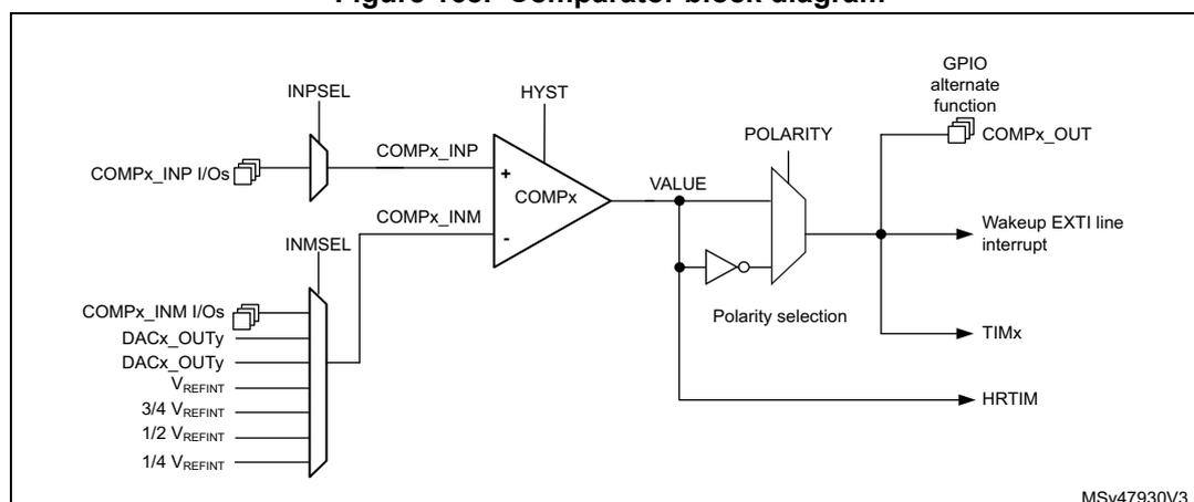
24.3.2 COMP pins and internal signals
The I/Os used as comparators inputs must be configured in analog mode in the GPIOs registers.
The comparator output can be connected to the I/Os using the alternate function channel given in “Alternate function mapping” table in the datasheet.
The output can also be internally redirected to a variety of timer input for the following purposes:
- • Emergency shut-down of PWM signals, using BKIN and BKIN2 inputs
- • Cycle-by-cycle current control, using OCREF_CLR inputs
- • Input capture for timing measures
It is possible to have the comparator output simultaneously redirected internally and externally.
Table 199. COMPx non-inverting input assignment
| INPSEL | COMP1_INP_ | COMP2_INP_ | COMP3_INP_ | COMP4_INP_ | COMP5_INP_ | COMP6_INP_ | COMP7_INP_ |
|---|---|---|---|---|---|---|---|
| 0 | PA1 | PA7 | PA0 | PB0 | PB13 | PB11 | PB14 |
| 1 | PB1 | PA3 | PC1 | PE7 | PD12 | PD11 | PD14 |
Table 200. COMPx inverting input assignment
| INMSEL [2:0] | COMP1_INM_ | COMP2_INM_ | COMP3_INM_ | COMP4_INM_ | COMP5_INM_ | COMP6_INM_ | COMP7_INM_ |
|---|---|---|---|---|---|---|---|
| 000 | 1/4 V REFINT | ||||||
| 001 | 1/2 V REFINT | ||||||
| 010 | 3/4 V REFINT | ||||||
| 011 | V REFINT | ||||||
| 100 | DAC3_CH1 | DAC3_CH2 | DAC3_CH1 | DAC3_CH2 | DAC4_CH1 | DAC4_CH2 | DAC4_CH1 |
| 101 | DAC1_CH1 | DAC1_CH2 | DAC1_CH1 | DAC1_CH1 | DAC1_CH2 | DAC2_CH1 | DAC2_CH1 |
| 110 | PA4 | PA5 | PF1 | PE8 | PB10 | PD10 | PD15 |
| 111 | PA0 | PA2 | PC0 | PB2 | PD13 | PB15 | PB12 |
24.3.3 COMP reset and clocks
The COMP clock provided by the clock controller is synchronous with the APB2 clock.
There is no COMP-dedicated clock enable control bit in the RCC controller. Reset and clock enable bits are common for COMP and SYSCFG.
Note: Important: The polarity selection logic and the output redirection to the port works independently of APB clock. This allows the comparator to work even in Stop mode.
24.3.4 COMP LOCK mechanism
The comparators can be used for safety purposes, such as over-current or thermal protection. For applications having specific functional safety requirements, it is necessary to insure that the comparator programming cannot be altered in case of spurious register access or program counter corruption.
For this purpose, the comparator control and status registers can be write-protected (read-only).
Once the programming is completed, the COMPx LOCK bit can be set. This causes the whole register to become read-only, including the COMPx LOCK bit.
The write protection can only be removed by an MCU reset.
24.3.5 COMP hysteresis
The comparator includes a programmable hysteresis to avoid spurious output transitions with noisy input signals. It is non-symmetrical and only acting to falling edge of the comparator output. The internal hysteresis function can be disabled so as to set the amount of hysteresis with external components, which can be useful for example when exiting a low-power mode.
Figure 169. Comparator hysteresis
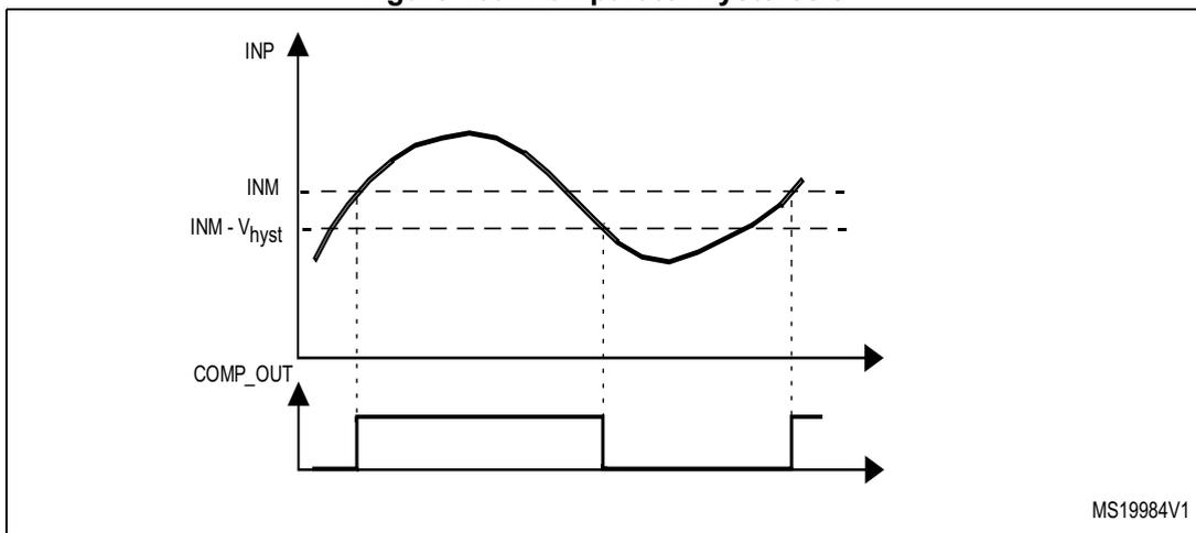
MS19984V1
24.3.6 COMP output blanking
The purpose of the blanking function is to prevent the current regulation from tripping upon short current spikes at the beginning of PWM period (typically the recovery current in power switch anti-parallel diodes). This goes through setting a dead window defined with a timer output compare signal. The blanking source is selected individually per comparator channel by software through BLANKSEL[2:0] bitfield of corresponding COMP_CxCSR register, as shown in Table 201: Blanking sources . The inverted blanking signal is logical AND-ed with the comparator stage output to produce the comparator channel x output. See the example provided in the following figure.
Figure 170. Comparator output blanking
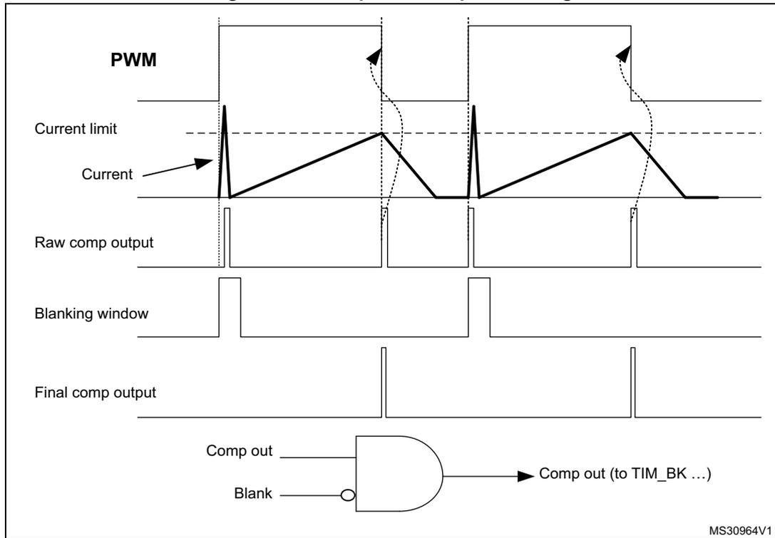
The diagram illustrates the timing relationship between a PWM signal, current limit, actual current, raw comparator output, a blanking window, and the final comparator output. The PWM signal is a square wave. The current limit is a dashed horizontal line. The current is a sawtooth-like waveform that rises when PWM is high and falls when PWM is low, bounded by the current limit. The raw comp output is a pulse that goes high when the current exceeds the current limit. The blanking window is a pulse that is high during the rising edge of the PWM. The final comp output is the result of an AND gate with inputs from the raw comp output and the inverted blanking window. The logic diagram at the bottom shows 'Comp out' and 'Blank' (with an inversion circle) as inputs to an AND gate, with the output labeled 'Comp out (to TIM_BK ...)'.
MS30964V1
Table 201. Blanking sources
| BLANKSEL [2:0] | COMP1 | COMP2 | COMP3 | COMP4 | COMP5 | COMP6 | COMP7 |
|---|---|---|---|---|---|---|---|
| 001 | TIM1_OC5 | TIM1_OC5 | TIM1_OC5 | TIM3_OC4 | TIM2_OC3 | TIM8_OC5 | TIM1_OC5 |
| 010 | TIM2_OC3 | TIM2_OC3 | TIM3_OC3 | TIM8_OC5 | TIM8_OC5 | TIM2_OC4 | TIM8_OC5 |
| 011 | TIM3_OC3 | TIM3_OC3 | TIM2_OC4 | TIM15_OC1 | TIM3_OC3 | TIM15_OC2 | TIM3_OC3 |
| 100 | TIM8_OC5 | TIM8_OC5 | TIM8_OC5 | TIM1_OC5 | TIM1_OC5 | TIM1_OC5 | TIM15_OC2 |
| 101 | TIM20_OC5 | TIM20_OC5 | TIM20_OC5 | TIM20_OC5 | TIM20_OC5 | TIM20_OC5 | TIM20_OC5 |
| 110 | TIM15_OC1 | TIM15_OC1 | TIM15_OC1 | TIM15_OC1 | TIM15_OC1 | TIM15_OC1 | TIM15_OC1 |
| 111 | TIM4_OC3 | TIM4_OC3 | TIM4_OC3 | TIM4_OC3 | TIM4_OC3 | TIM4_OC3 | TIM4_OC3 |
24.4 COMP low-power modes
Table 202. Comparator behavior in low-power modes
| Mode | Description |
|---|---|
| Sleep | No effect on the comparators. Comparator interrupts cause the device to exit the Sleep mode. |
| Low-power run | No effect. |
Table 202. Comparator behavior in low-power modes (continued)
| Mode | Description |
|---|---|
| Low-power sleep | No effect. COMP interrupts cause the device to exit the Low-power sleep mode. |
| Stop | No effect on the comparators. Comparator interrupts cause the device to exit the Stop mode. |
| Standby, Shutdown | The COMP registers are powered down and must be reinitialized after exiting Standby or Shutdown mode. |
24.5 COMP interrupts
The comparator outputs are internally connected to the Extended interrupts and events controller. Each comparator has its own EXTI line and can generate either interrupts or events. The same mechanism is used to exit Sleep and Stop low-power modes.
Refer to Interrupt and events section for more details.
To enable the COMPx interrupt, it is required to follow this sequence:
- 1. Configure and enable the EXTI line corresponding to the COMPx output event in interrupt mode and select sensitivity to rising edge, falling edge or to both edges
- 2. Configure and enable the NVIC IRQ channel mapped to the corresponding EXTI lines
- 3. Enable COMPx
Interrupt events are flagged through flags in EXTI_PR1/EXTI_PR2 registers.
24.6 COMP registers
24.6.1 Comparator x control and status register (COMP_CxCSR)
For x = 1 through 7, the COMP_CxCSR register contains all bits and flags related to the comparator x.
Address offset: 4(x-1), where x = 1 to 7
System reset value: 0x0000 0000
| 31 | 30 | 29 | 28 | 27 | 26 | 25 | 24 | 23 | 22 | 21 | 20 | 19 | 18 | 17 | 16 |
|---|---|---|---|---|---|---|---|---|---|---|---|---|---|---|---|
| LOCK | VALUE | Res. | Res. | Res. | Res. | Res. | Res. | SCALEN | BRGEN | BLANKSEL[2:0] | HYST[2:0] | ||||
| rw | r | rw | rw | rw | rw | rw | rw | rw | rw | ||||||
| 15 | 14 | 13 | 12 | 11 | 10 | 9 | 8 | 7 | 6 | 5 | 4 | 3 | 2 | 1 | 0 |
|---|---|---|---|---|---|---|---|---|---|---|---|---|---|---|---|
| POL | Res. | Res. | Res. | Res. | Res. | Res. | INPSEL | Res. | INMSEL[2:0] | Res. | Res. | Res. | EN | ||
| rw | rw | rw | rw | rw | rw | ||||||||||
This bit is set by software and cleared by a hardware system reset. It locks the whole content of the comparator x control register COMP_CxCSR[31:0]. When locked, all control bits and flags can be read only but not written. When unlocked, the control bits can also be written by software.
0: Unlock
1: Lock
Bit 30 VALUE: Comparator x output statusThis read-only flag reflects the level of the comparator x output before the polarity selector and blanking, as indicated in Figure 168 .
Bits 29:24 Reserved, must be kept at reset value
Bit 23 SCALEN: V REFINT scaler enableThis bit controlled by software enables the operation of V REFINT scaler at the inverting input of all comparator. To disable the V REFINT scaler, SCALEN bits of all COMP_CxCSR registers must be set to Disable state. When the V REFINT scaler is disabled, the 1/4 V REFINT , 1/2 V REFINT , 3/4 V REFINT and V REFINT inputs of the multiplexer should not be selected.
0: Disable
1: Enable
Bit 22 BRGEN: V REFINT scaler resistor bridge enableThis bit controlled by software enables the operation of resistor bridge in the V REFINT scaler. To disable the resistor bridge, BRGEN bits of all COMP_CxCSR registers must be set to Disable state. When the resistor bridge is disabled, the 1/4 V REFINT , 1/2 V REFINT , and 3/4 V REFINT inputs of the input selector receive V REFINT voltage.
0: Disable
1: Enable
Bits 21:19 BLANKSEL[2:0]: Comparator x blanking signal selectThis bitfield controlled by software selects the blanking signal for comparator channel x, as shown in Table 201: Blanking sources .
Bits 18:16 HYST[2:0]: Comparator x hysteresisThis bitfield controlled by software selects the hysteresis of the comparator x:
000: No hysteresis
001: 10mV hysteresis
010: 20mV hysteresis
011: 30mV hysteresis
100: 40mV hysteresis
101: 50mV hysteresis
110: 60mV hysteresis
111: 70mV hysteresis
Bit 15 POL: Comparator x polarityThis bit controlled by software selects the comparator x output polarity:
0: Non-inverted
1: Inverted
Bits 14:9 Reserved, must be kept at reset value
Bit 8 INPSEL: Comparator x signal select for non-inverting inputThis bitfield controlled by software selects the signal for the non-inverting input COMPx_INP of the comparator x, as shown in Table 199: COMPx non-inverting input assignment .
Bit 7 Reserved, must be kept at reset value
Bits 6:4 INMSEL[2:0] : Comparator x signal select for inverting input
This bitfield controlled by software selects the signal for the inverting input COMPx_INM of the comparator x, as shown in Table 200: COMPx inverting input assignment .
Bits 3:1 Reserved, must be kept at reset value
Bit 0 EN : Comparator x enable
This bit controlled by software enables the operation of comparator x:
0: Disable
1: Enable
24.6.2 COMP register map
The following table summarizes the comparator registers.
The comparator registers share SYSCFG peripheral register base addresses.
Table 203. COMP register map and reset values
| Offset | Register | 31 | 30 | 29 | 28 | 27 | 26 | 25 | 24 | 23 | 22 | 21 | 20 | 19 | 18 | 17 | 16 | 15 | 14 | 13 | 12 | 11 | 10 | 9 | 8 | 7 | 6 | 5 | 4 | 3 | 2 | 1 | 0 |
|---|---|---|---|---|---|---|---|---|---|---|---|---|---|---|---|---|---|---|---|---|---|---|---|---|---|---|---|---|---|---|---|---|---|
| 0x00 | COMP_C1CSR | LOCK | VALUE | Res | Res | Res | Res | Res | Res | SCALEN | BRGEN | BLANKSEL[2:0] | HYST[2:0] | POL | Res | Res | Res | Res | Res | Res | INPSEL | Res | INMSEL[2:0] | Res | Res | Res | EN | ||||||
| Reset value | 0 | 0 | 0 | 0 | 0 | 0 | 0 | 0 | 0 | 0 | 0 | 0 | 0 | 0 | 0 | 0 | |||||||||||||||||
| 0x04 | COMP_C2CSR | LOCK | VALUE | Res | Res | Res | Res | Res | Res | SCALEN | BRGEN | BLANKSEL[2:0] | HYST[2:0] | POL | Res | Res | Res | Res | Res | Res | INPSEL | Res | INMSEL[2:0] | Res | Res | Res | EN | ||||||
| Reset value | 0 | 0 | 0 | 0 | 0 | 0 | 0 | 0 | 0 | 0 | 0 | 0 | 0 | 0 | 0 | 0 | |||||||||||||||||
| 0x08 | COMP_C3CSR | LOCK | VALUE | Res | Res | Res | Res | Res | Res | SCALEN | BRGEN | BLANKSEL[2:0] | HYST[2:0] | POL | Res | Res | Res | Res | Res | Res | INPSEL | Res | INMSEL[2:0] | Res | Res | Res | EN | ||||||
| Reset value | 0 | 0 | 0 | 0 | 0 | 0 | 0 | 0 | 0 | 0 | 0 | 0 | 0 | 0 | 0 | 0 | |||||||||||||||||
| 0x0C | COMP_C4CSR | LOCK | VALUE | Res | Res | Res | Res | Res | Res | SCALEN | BRGEN | BLANKSEL[2:0] | HYST[2:0] | POL | Res | Res | Res | Res | Res | Res | INPSEL | Res | INMSEL[2:0] | Res | Res | Res | EN | ||||||
| Reset value | 0 | 0 | 0 | 0 | 0 | 0 | 0 | 0 | 0 | 0 | 0 | 0 | 0 | 0 | 0 | 0 | |||||||||||||||||
| 0x10 | COMP_C5CSR | LOCK | VALUE | Res | Res | Res | Res | Res | Res | SCALEN | BRGEN | BLANKSEL[2:0] | HYST[2:0] | POL | Res | Res | Res | Res | Res | Res | INPSEL | Res | INMSEL[2:0] | Res | Res | Res | EN | ||||||
| Reset value | 0 | 0 | 0 | 0 | 0 | 0 | 0 | 0 | 0 | 0 | 0 | 0 | 0 | 0 | 0 | 0 | |||||||||||||||||
Table 203. COMP register map and reset values (continued)
| Offset | Register | 31 | 30 | 29 | 28 | 27 | 26 | 25 | 24 | 23 | 22 | 21 | 20 | 19 | 18 | 17 | 16 | 15 | 14 | 13 | 12 | 11 | 10 | 9 | 8 | 7 | 6 | 5 | 4 | 3 | 2 | 1 | 0 |
|---|---|---|---|---|---|---|---|---|---|---|---|---|---|---|---|---|---|---|---|---|---|---|---|---|---|---|---|---|---|---|---|---|---|
| 0x14 | COMP_C6CSR | LOCK | VALUE | Res. | Res. | Res. | Res. | Res. | Res. | SCALEN | BRGEN | BLANKSEL[2:0] | HYST[2:0] | POL | Res. | Res. | Res. | Res. | Res. | Res. | INPSEL. | Res. | INMSEL[2:0] | Res. | Res. | Res. | EN | ||||||
| Reset value | 0 | 0 | 0 | 0 | 0 | 0 | 0 | 0 | 0 | 0 | 0 | 0 | 0 | 0 | 0 | 0 | |||||||||||||||||
| 0x18 | COMP_C7CSR | LOCK | VALUE | Res. | Res. | Res. | Res. | Res. | Res. | SCALEN | BRGEN | BLANKSEL[2:0] | HYST[2:0] | POL | Res. | Res. | Res. | Res. | Res. | Res. | INPSEL. | Res. | INMSEL[2:0] | Res. | Res. | Res. | EN | ||||||
| Reset value | 0 | 0 | 0 | 0 | 0 | 0 | 0 | 0 | 0 | 0 | 0 | 0 | 0 | 0 | 0 | 0 | |||||||||||||||||
Refer to Section 2.2.2: Memory map and register boundary addresses for the register boundary addresses.