7. Reset and clock control (RCC)
7.1 Reset
There are three types of reset, defined as system reset, power reset and RTC domain reset.
7.1.1 Power reset
A power reset is generated when one of the following events occurs:
- 1. Power-on reset (POR) or brown-out reset (BOR)
- 2. When exiting from Standby mode
- 3. When exiting from Shutdown mode
A brown-out reset, including power-on or power-down reset (POR/PDR), sets all registers to their reset values except the RTC domain.
When exiting Standby mode, all registers in the \( V_{CORE} \) domain are set to their reset value. Registers outside the \( V_{CORE} \) domain (RTC, WKUP, IWDG, and Standby/Shutdown modes control) are not impacted.
When exiting Shutdown mode, a brown-out reset is generated, resetting all registers except those in the RTC domain.
7.1.2 System reset
A system reset sets all registers to their reset values unless specified otherwise in the register description. This reset is generated when one of the following events occurs:
- 1. A low level on the NRST pin (external reset)
- 2. Window watchdog event (WWDG reset)
- 3. Independent watchdog event (IWDG reset)
- 4. A software reset (SW reset) (see Software reset )
- 5. Low-power mode security reset (see Low-power mode security reset )
- 6. Option byte loader reset (see Option byte loader reset )
- 7. A brown-out reset
The reset source can be identified by checking the reset flags in the Control/Status register, RCC_CSR (see Section 7.4.28 ).
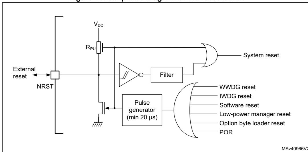
NRST pin (external reset)
Through specific option bits (NRST_MODE), the NRST pin is configurable for operating as:
- • Reset input/output (default at device delivery)
Any valid reset signal on the pin is propagated to device internal logic and all internal reset sources are externally driven through a pulse generator to this pin. The GPIO functionality (PG10) is not available. The pulse generator guarantees a minimum reset pulse duration of 20 µs for each internal reset source to be output on the NRST pin. An internal reset holder option can be used, if enabled in the option bytes, to ensure that the pin is pulled low until its voltage meets VIL threshold. This function guarantee the detection of internal reset sources by external components when the line faces a significant capacitive load. In case on an internal reset, the internal pull-up RPU is deactivated in order to save the power consumption through the pull-up resistor. This
mode is always active (independently of the option bytes setting) during each device power-on-reset (until option bytes are loaded): power on the device or wake up from Shutdown mode.
- •
Reset input
In this mode, any valid reset signal on the NRST pin is propagated to device internal logic, but resets generated internally by the device are not visible on the pin. In this configuration, GPIO functionality (PG10) is not available. - •
GPIO
In this mode, the pin can be used as PG10 standard GPIO. The reset function of the pin is not available. Reset is only possible from device internal reset sources and it is not propagated to the pin.
Figure 16. Simplified diagram of the reset circuit
Software reset
The SYSRESETREQ bit in Cortex ® -M4 with FPU Application Interrupt and Reset Control Register must be set to force a software reset on the device (refer to the STM32F3xx/F4xx/L4xx Cortex ® -M4 programming manual (PM0214)).
Low-power mode security reset
To prevent that critical applications mistakenly enter a low-power mode, two low-power mode security resets are available. If enabled in option bytes, the resets are generated in the following conditions:
- 1. Entering Standby mode: this type of reset is enabled by resetting nRST_STDBY bit in User option Bytes. In this case, whenever a Standby mode entry sequence is successfully executed, the device is reset instead of entering Standby mode.
- 2. Entering Stop mode: this type of reset is enabled by resetting nRST_STOP bit in User option bytes. In this case, whenever a Stop mode entry sequence is successfully executed, the device is reset instead of entering Stop mode.
- 3. Entering Shutdown mode: this type of reset is enabled by resetting nRST_SHDW bit in User option bytes. In this case, whenever a Shutdown mode entry sequence is successfully executed, the device is reset instead of entering Shutdown mode.
For further information on the user option bytes refer to Section 3.4.1 .
Option byte loader reset
The option byte loader reset is generated when the OBL_LAUNCH bit (bit 27) is set in the FLASH_CR register. This bit is used to launch the option byte loading by software.
7.1.3 RTC domain reset
The RTC domain has two specific resets.
A RTC domain reset is generated when one of the following events occurs:
- 1. Software reset, triggered by setting the BDRST bit in the RTC domain control register (RCC_BDCR) .
- 2. V DD or V BAT power on, if both supplies have previously been powered off.
A RTC domain reset only affects the LSE oscillator, the RTC, the Backup registers and the RCC RTC domain control register.
7.2 Clocks
Three different clock sources can be used to drive the system clock (SYSCLK):
- • HSI16 (high speed internal) 16 MHz RC oscillator clock
- • HSE oscillator clock, from 4 to 48 MHz
- • PLL clock
The HSI16 is used as system clock source after startup from Reset.
The devices have the following additional clock sources:
- • 32 kHz low speed internal RC (LSI RC) which drives the independent watchdog and optionally the RTC used for Auto-wake-up from Stop and Standby modes.
- • 32.768 kHz low speed external crystal (LSE crystal) which optionally drives the real-time clock (RTCCLK).
- • RC 48 MHz internal clock sources (HSI48) to potentially drive the USB FS and the RNG.
Each clock source can be switched on or off independently when it is not used, to optimize power consumption.
Several prescalers can be used to configure the AHB frequency, the APB1 and APB2 domains. The maximum frequency of AHB, APB1, and APB2 domains is 170 MHz.
All the peripheral clocks are derived from their bus clock (HCLK, PCLK1 or PCLK2) except:
- • The 48 MHz clock, used for USB device FS, and RNG. This clock is derived (selected by software) from one of the four following sources:
- – PLL “Q” clock
- – HSI48 internal oscillator
When available, the HSI48 48 MHz clock can be coupled to the clock recovery system allowing adequate clock connection for the USB OTG FS (Crystal less solution).
- • The ADCs clock which is derived (selected by software) from one of the following sources:
- – System clock (SYSCLK)
- – PLL “P” clock
- • The U(S)ARTs clocks which are derived (selected by software) from one of the four following sources:
- – System clock (SYSCLK)
- – HSI16 clock
- – LSE clock
- – APB1 or APB2 clock (PCLK1 or PCLK2 depending on which APB is mapped the U(S)ART)
The wake-up from Stop mode is supported only when the clock is HSI16 or LSE.
- • The I
2
Cs clocks which are derived (selected by software) from one of the three following sources:
- – System clock (SYSCLK)
- – HSI16 clock
- – APB1 clock (PCLK1)
The wake-up from Stop mode is supported only when the clock is HSI16.
- • The SAI1 clock which is derived (selected by software) from one of the following sources:
- – an external clock mapped on I2S_CKIN
- – System clock
- – PLL “Q” clock
- – HSI16 clock
- • The QUADSPI kernel clock which is derived (selected by software) from one of the following sources:
- – System clock,
- – PLL “Q” clock
- – HSI16 clock
- • The low-power timer (LPTIM1) clock which is derived (selected by software) from one of the five following sources:
- – LSI clock
- – LSE clock
- – HSI16 clock
- – APB1 clock (PCLK1)
- – External clock mapped on LPTIMx_IN1
The functionality in Stop mode (including wake-up) is supported only when the clock is
LSI or LSE, or in external clock mode.
- • The RTC clock which is derived (selected by software) from one of the three following sources:
- – LSE clock
- – LSI clock
- – HSE clock divided by 32
The functionality in Stop mode (including wake-up) is supported only when the clock is LSI or LSE.
- • The IWDG clock which is always the LSI clock.
- • The UCPD1 clock, which is derived from HSI16 clock.
- • The FDCAN1 clock, which is derived (selected by software) from one of the two following sources:
- – HSE clock
- – PLL “Q” clock
- – PCLK clock
The RCC feeds the Cortex ® System Timer (SysTick) external clock with the AHB clock (HCLK) divided by 8. The SysTick can work either with this clock or directly with the Cortex ® clock (HCLK), configurable in the SysTick Control and Status Register.
FCLK acts as Cortex ® -M4 with FPU free-running clock. For more details refer to the Cortex ® -M4 programming manual (PM0214).
Figure 17. Clock tree
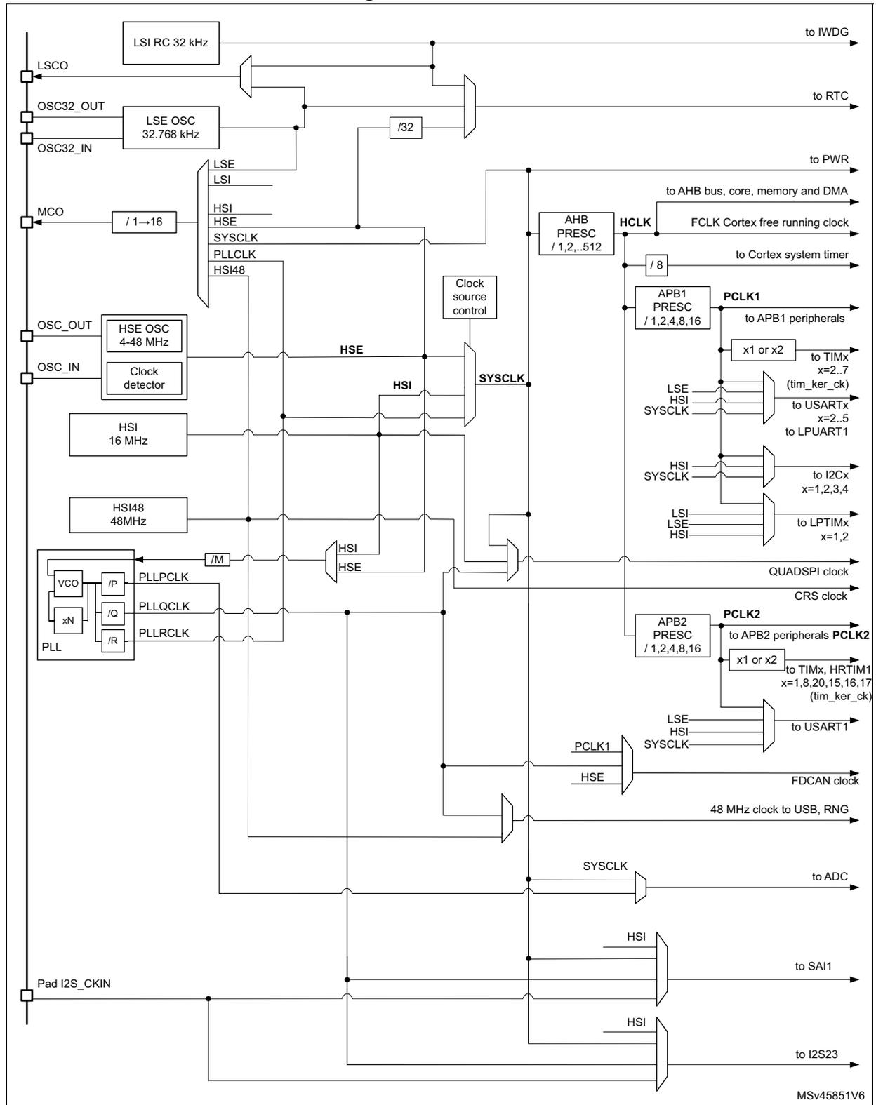
The diagram illustrates the internal clock architecture of the RM0440. On the left, various clock sources are shown:
- LSI RC 32 kHz : Connected to the IWDG and RTC.
- LSE OSC 32.768 kHz : Connected via OSC32_IN and OSC32_OUT pins to the RTC and PWR.
- HSE OSC 4-48 MHz : Connected via OSC_IN and OSC_OUT pins, with a clock detector. It can be divided by /32 for the RTC.
- HSI 16 MHz and HSI48 48 MHz : Internal high-speed oscillators.
- PLL : A phase-locked loop consisting of a VCO, multipliers (/P, /Q, /R), and a divider (/M). It generates PLLPCLK, PLLQCLK, and PLLRCLK.
- MCO : Microcontroller clock output pin, selectable from LSE, LSI, HSI, HSE, SYSCLK, PLLCLK, or HSI48, with a divider of /1 to /16.
- Pad I2S_CKIN : External clock input for I2S.
- The AHB bus, core, memory and DMA via HCLK .
- The Cortex system timer via FCLK (derived from HCLK).
- APB1 peripherals via PCLK1 (derived from HCLK with a prescaler of /1,2,4,8,16).
- APB2 peripherals via PCLK2 (derived from HCLK with a prescaler of /1,2,4,8,16).
- ADC via SYSCLK.
- SAI1 and I2S23 via HSI.
- QUADSPI clock , CRS clock , and FDCAN clock via PCLK1.
- A 48 MHz clock to USB, RNG derived from HSE or PLL.
- TIMx (x=2..7, tim_ker_ck) via PCLK1 (x1 or x2).
- USARTx (x=2..5) and LPUART1 via LSE, HSI, or SYSCLK.
- I2Cx (x=1,2,3,4) via HSI or SYSCLK.
- LPTIMx (x=1,2) via LSI, LSE, or HSI.
- HRTIM1 (x=1,8,20,15,16,17, tim_ker_ck) via PCLK2 (x1 or x2).
- USART1 via LSE, HSI, or SYSCLK.
1. For full details about the internal and external clock source characteristics, refer to the “Electrical
characteristics" section of the datasheet.
- 2. The ADC clock can be derived from the AHB clock of the ADC bus interface, divided by a programmable factor (1, 2 or 4). When the programmable factor is 1, the AHB prescaler must be equal to 1.
7.2.1 HSE clock
The high speed external clock signal (HSE) can be generated from two possible clock sources:
- • HSE external crystal/ceramic resonator
- • HSE user external clock
The resonator and the load capacitors have to be placed as close as possible to the oscillator pins to minimize output distortion and startup stabilization time. The loading capacitance values must be adjusted according to the selected oscillator.
Figure 18. HSE/ LSE clock sources
| Clock source | Hardware configuration |
|---|---|
| External clock | 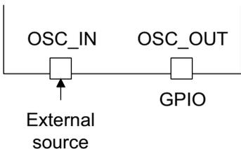 The diagram shows a microcontroller with two pins labeled OSC_IN and OSC_OUT. OSC_IN is connected to an external source, and OSC_OUT is connected to a GPIO pin. The reference code MSv31915V1 is shown in the bottom right corner. |
| Crystal/Ceramic resonators | 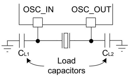 The diagram shows a microcontroller with two pins labeled OSC_IN and OSC_OUT. A crystal/ceramic resonator is connected between these pins. Two load capacitors, labeled CL1 and CL2, are connected from each pin to ground. The reference code MSv31916V1 is shown in the bottom right corner. |
External crystal/ceramic resonator (HSE crystal)
The 4 to 48 MHz external oscillator has the advantage of producing a very accurate rate on the main clock. The associated hardware configuration is shown in Figure 18 . Refer to the electrical characteristics section of the datasheet for more details.
The HSERDY flag in the Clock control register (RCC_CR) indicates if the HSE oscillator is stable or not. At startup, the clock is not released until this bit is set by hardware. An interrupt can be generated if enabled in the Clock interrupt enable register (RCC_CIER) .
The HSE Crystal can be switched on and off using the HSEON bit in the Clock control register (RCC_CR) .
External source (HSE bypass)
In this mode, an external clock source must be provided. It can have a frequency of up to 48 MHz. You select this mode by setting the HSEBYP and HSEON bits in the Clock control register (RCC_CR) . The external clock signal (square, sinus or triangle) with ~40-60 % duty cycle depending on the frequency (refer to the datasheet ) has to drive the OSC_IN pin while the OSC_OUT pin can be used as GPIO. See Figure 18 .
7.2.2 HSI16 clock
The HSI16 clock signal is generated from an internal 16 MHz RC Oscillator.
The HSI16 RC oscillator has the advantage of providing a clock source at low cost (no external components). It also has a faster startup time than the HSE crystal oscillator however, even with calibration the frequency is less accurate than an external crystal oscillator or ceramic resonator.
The HSI16 clock can be selected as system clock after wake-up from Stop modes (Stop 0, Stop 1), see Section 7.3 . It can also be used as a backup clock source (auxiliary clock) if the HSE crystal oscillator fails. Refer to Section 7.2.9 .
Calibration
RC oscillator frequencies can vary from one chip to another due to manufacturing process variations, this is why each device is factory calibrated by ST for 1 % accuracy at \( T_A=25^\circ\text{C} \) .
After reset, the factory calibration value is loaded in the HSICAL[7:0] bits in the Internal clock sources calibration register (RCC_ICSCR) .
If the application is subject to voltage or temperature variations this may affect the RC oscillator speed. You can trim the HSI16 frequency in the application using the HSITRIM[6:0] in the Internal clock sources calibration register (RCC_ICSCR) .
For more details on how to measure the HSI16 frequency variation, refer to Section 7.2.16 .
The HSIRDY flag in the Clock control register (RCC_CR) indicates if the HSI16 oscillator is stable or not. At startup, the HSI16 output clock is not released until this bit is set by hardware.
The HSI16 oscillator can be switched on and off using the HSION bit in the Clock control register (RCC_CR) .
The HSI16 signal can also be used as a backup source (Auxiliary clock) if the HSE crystal oscillator fails. Refer to Section 7.2.9 .
7.2.3 HSI48 clock
The HSI48 clock signal is generated from an internal 48 MHz RC oscillator and can be used directly for USB and for random number generator (RNG).
The internal 48 MHz RC oscillator is mainly dedicated to provide a high precision clock to the USB peripheral by means of a special Clock Recovery System (CRS) circuitry. The CRS can use the LSE or an external signal to automatically and quickly adjust the oscillator frequency on-fly. It is disabled as soon as the system enters Stop or Standby mode. When the CRS is not used, the HSI48 RC oscillator runs on its default frequency which is subject to manufacturing process variations.
The HSI48RDY flag in the Clock recovery RC register (RCC_CRRRCR) indicates whether the HSI48 RC oscillator is stable or not. At startup, the HSI48 RC oscillator output clock is not released until this bit is set by hardware.
The HSI48 can be switched on and off using the HSI48ON bit in the Clock recovery RC register (RCC_CRRRCR).
7.2.4 PLL
The internal PLL can be used to multiply the HSI16 or HSE output clock frequency. The PLL input frequency must be within the range defined in the device datasheet. The selected clock source is divided by a programmable factor PLLM from 1 to 8 to provide a clock frequency in the requested input range. Refer to Figure 17 and PLL configuration register (RCC_PLLCFGR) .
The PLL configuration (selection of the input clock and multiplication factor) must be done before enabling the PLL. Once the PLL is enabled, these parameters cannot be changed.
To modify the PLL configuration, proceed as follows:
- 1. Disable the PLL by setting PLLON to 0 in Clock control register (RCC_CR) .
- 2. Wait until PLLRDY is cleared. The PLL is now fully stopped.
- 3. Change the desired parameter.
- 4. Enable the PLL again by setting PLLON to 1.
- 5. Enable the desired PLL outputs by configuring PLLPEN, PLLQEN, PLLREN in PLL configuration register (RCC_PLLCFGR) .
An interrupt can be generated when the PLL is ready, if enabled in the Clock interrupt enable register (RCC_CIER) .
The PLL output frequency must not exceed 170 MHz.
The enable bit of each PLL output clock (PLLPEN, PLLQEN, PLLREN) can be modified at any time without stopping the corresponding PLL. PLLREN cannot be cleared if PLLCLK is used as system clock.
7.2.5 LSE clock
The LSE crystal is a 32.768 kHz Low Speed External crystal or ceramic resonator. It has the advantage of providing a low-power but highly accurate clock source to the real-time clock peripheral (RTC) for clock/calendar or other timing functions.
The LSE crystal is switched on and off using the LSEON bit in RTC domain control register (RCC_BDCR) . The crystal oscillator driving strength can be changed at runtime using the LSEDRV[1:0] bits in the RTC domain control register (RCC_BDCR) to obtain the best
compromise between robustness and short start-up time on one side and low-power-consumption on the other side. The LSE drive can be decreased to the lower drive capability (LSEDRV = 00) when the LSE is ON. However, once LSEDRV is selected, the drive capability can not be increased if LSEON = 1.
The LSERDY flag in the RTC domain control register (RCC_BDCR) indicates whether the LSE crystal is stable or not. At startup, the LSE crystal output clock signal is not released until this bit is set by hardware. An interrupt can be generated if enabled in the Clock interrupt enable register (RCC_CIER) .
External source (LSE bypass)
In this mode, an external clock source must be provided. It can have a frequency of up to 1 MHz. You select this mode by setting the LSEBYP and LSEON bits in the AHB1 peripheral clocks enable in Sleep and Stop modes register (RCC_AHB1SMENR) . The external clock signal (square, sinus or triangle) with ~50 % duty cycle has to drive the OSC32_IN pin while the OSC32_OUT pin can be used as GPIO. See Figure 18 .
7.2.6 LSI clock
The LSI RC acts as a low-power clock source that can be kept running in Stop and Standby mode for the independent watchdog (IWDG) and RTC. The clock frequency is 32 kHz. For more details, refer to the electrical characteristics section of the datasheets.
The LSI RC can be switched on and off using the LSION bit in the Control/status register (RCC_CSR) .
The LSIRDY flag in the Control/status register (RCC_CSR) indicates if the LSI oscillator is stable or not. At startup, the clock is not released until this bit is set by hardware. An interrupt can be generated if enabled in the Clock interrupt enable register (RCC_CIER) .
7.2.7 System clock (SYSCLK) selection
Four different clock sources can be used to drive the system clock (SYSCLK):
- • HSI16 oscillator
- • HSE oscillator
- • PLL
The system clock maximum frequency is 170 MHz. After a system reset, the HSI16 oscillator is selected as system clock. When a clock source is used directly or through the PLL as a system clock, it is not possible to stop it.
A switch from one clock source to another occurs only if the target clock source is ready (clock stable after startup delay or PLL locked). If a clock source which is not yet ready is selected, the switch occurs when the clock source becomes ready. Status bits in the RCC_CR and RCC_CFGR registers indicate which clock(s) is (are) ready and which clock is currently used as a system clock.
To switch from low speed to high speed or from high speed to low speed system clock, it is recommended to use a transition state with medium speed clock, for at least 1 µs.
Clock source switching conditions:
- • Switching from HSE or HSI16 to PLL with AHB frequency (HCLK) higher than 80 MHz
- • Switching from PLL with HCLK higher than 80 MHz to HSE or HSI16
Transition state:
- • Set the AHB prescaler HPRE[3:0] bits to divide the system frequency by 2
- • Switch system clock to PLL
- • Wait at least 1 µs and then reconfigure AHB prescaler bits to the needed HCLK frequency
7.2.8 Clock source frequency versus voltage scaling
Table 50 gives the clock source frequencies, depending upon the product voltage range.
Table 50. Clock source frequency
| Product voltage range | Clock frequency | ||
|---|---|---|---|
| HSI16 | HSE | PLL | |
| Range 1 Boost mode | 16 MHz | 48 MHz | 170 MHz |
| Range 1 normal mode | 16 MHz | 48 MHz | 150 MHz |
| Range 2 | 16 MHz | 26 MHz | 26 MHz |
7.2.9 Clock security system (CSS)
Clock Security System can be activated by software. In this case, the clock detector is enabled after the HSE oscillator startup delay, and disabled when this oscillator is stopped.
If a failure is detected on the HSE clock, the HSE oscillator is automatically disabled, a clock failure event is sent to the break input of the advanced-control timers (TIM1/TIM8/TIM20 and TIM15/16/17) and to the hrtim_sys_flt, and an interrupt is generated to inform the software about the failure (Clock Security System Interrupt CSSI), allowing the MCU to perform rescue operations. The CSSI is linked to the Cortex®-M4 with FPU NMI (Non-Maskable Interrupt) exception vector.
Note: Once the CSS is enabled and if the HSE clock fails, the CSS interrupt occurs and a NMI is automatically generated. The NMI is executed indefinitely unless the CSS interrupt pending bit is cleared. As a consequence, in the NMI ISR user must clear the CSS interrupt by setting the CSSC bit in the Clock interrupt clear register (RCC_CICR).
If the HSE oscillator is used directly or indirectly as the system clock (indirectly means: it is used as PLL input clock, and the PLL clock is used as system clock), a detected failure causes a switch of the system clock to the HSI16 oscillator, and the disabling of the HSE oscillator. If the HSE clock (divided or not) is the clock entry of the PLL used as system clock when the failure occurs, the PLL is disabled too.
7.2.10 Clock security system on LSE
A Clock Security System on LSE can be activated by software writing the LSECSSON bit in the Control/status register (RCC_CSR) . This bit can be disabled only by a hardware reset or RTC software reset, or after a failure detection on LSE. LSECSSON must be written after LSE and LSI are enabled (LSEON and LSION enabled) and ready (LSERDY and LSIRDY set by hardware), and after the RTC clock has been selected by RTCSEL.
The CSS on LSE is working in all modes except VBAT. It is working also under system reset (excluding power on reset). If a failure is detected on the external 32 kHz oscillator, the LSE
clock is no longer supplied to the RTC but no hardware action is made to the registers. If the HSI16 was in PLL-mode, this mode is disabled.
In Standby mode a wake-up is generated. In other modes an interrupt can be sent to wake up the software (see Clock interrupt enable register (RCC_CIER) , Clock interrupt flag register (RCC_CIFR) , Clock interrupt clear register (RCC_CICR) ).
The software MUST then disable the LSECSSON bit, stop the defective 32 kHz oscillator (disabling LSEON), and change the RTC clock source (no clock or LSI or HSE, with RTCSEL), or take any required action to secure the application.
The frequency of LSE oscillator have to be higher than 30 kHz to avoid false positive CSS detection.
7.2.11 ADC clock
The ADC clock is derived from the system clock, or from the PLL “P” output. It can be divided by the following prescalers values: 1,2,4,6,8,10,12,16,32,64,128 or 256 by configuring the ADCx_CCR register. It is asynchronous to the AHB clock. Alternatively, the ADC clock can be derived from the AHB clock of the ADC bus interface, divided by a programmable factor (1, 2 or 4). This programmable factor is configured using the CKMODE bit fields in the ADCx_CCR.
If the programmed factor is 1, the AHB prescaler must be set to 1.
Refer to the device datasheet for the maximum ADC clock.
7.2.12 RTC clock
The RTCCLK clock source can be either the HSE/32, LSE or LSI clock. It is selected by programming the RTCSEL[1:0] bits in the RTC domain control register (RCC_BDCR) . This selection cannot be modified without resetting the RTC domain. The system must always be configured so as to get a PCLK frequency greater then or equal to the RTCCLK frequency for a proper operation of the RTC.
The LSE clock is in the RTC domain, whereas the HSE and LSI clocks are not. Consequently:
- • If LSE is selected as RTC clock:
- – The RTC continues to work even if the \( V_{DD} \) supply is switched off, provided the \( V_{BAT} \) supply is maintained.
- • If LSI is selected as the RTC clock:
- – The RTC state is not guaranteed if the \( V_{DD} \) supply is powered off.
- • If the HSE clock divided by a prescaler is used as the RTC clock:
- – The RTC state is not guaranteed if the \( V_{DD} \) supply is powered off or if the internal voltage regulator is powered off (removing power from the \( V_{CORE} \) domain).
When the RTC clock is LSE or LSI, the RTC remains clocked and functional under system reset.
7.2.13 Timer clock
The timer clock frequencies (tim_ker_ck) are automatically defined by hardware. If the APB prescaler equals 1, the timer clock frequencies are set to the same frequency of the APB domain, otherwise, they are set to twice ( \( \times 2 \) ) the frequency of the APB domain.
7.2.14 Watchdog clock
If the Independent watchdog (IWDG) is started by either hardware option or software access, the LSI oscillator is forced ON and cannot be disabled. After the LSI oscillator temporization, the clock is provided to the IWDG.
7.2.15 Clock-out capability
- • MCO
The microcontroller clock output (MCO) capability allows the clock to be output onto the external MCO pin. One of eight clock signals can be selected as the MCO clock.
- – LSI
- – LSE
- – SYSCLK
- – HSI16
- – HSI48
- – HSE
- – PLLCLK
The selection is controlled by the MCOSEL[3:0] bits of the Clock configuration register (RCC_CFGR) . The selected clock can be divided with the MCOPRE[2:0] field of the Clock configuration register (RCC_CFGR) .
- • LSCO
Another output (LSCO) allows a low speed clock to be output onto the external LSCO pin:
- – LSI
- – LSE
This output remains available in Stop (Stop 0 and Stop 1) and Standby modes. The selection is controlled by the LSCOSEL, and enabled with the LSCOEN in the RTC domain control register (RCC_BDCR) .
The MCO clock output requires the corresponding alternate function selected on the MCO pin, the LSCO pin should be left in default POR state.
7.2.16 Internal/external clock measurement with TIM5/TIM15/TIM16/TIM17
It is possible to indirectly measure the frequency of all on-board clock sources by mean of the TIM5, TIM15, TIM16 or TIM17 channel 1 input capture, as represented on Figure 19 , Figure 20 , Figure 21 and Figure 22 .
Figure 19. Frequency measurement with TIM15 in capture mode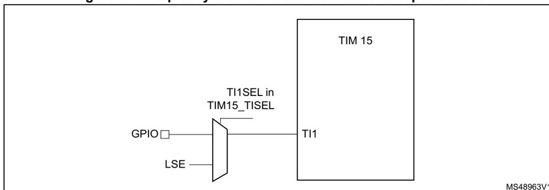
The diagram shows a multiplexer on the left with two inputs: 'GPIO' and 'LSE'. The output of the multiplexer is connected to the 'TI1' input of a block labeled 'TIM 15'. Above the multiplexer is the label 'TI1SEL in TIM15_TISEL'. In the bottom right corner of the diagram area, the text 'MS48963V1' is present.
The input capture channel of the Timer 15 can be a GPIO line or an internal clock of the MCU. The possibilities are the following ones:
- • TIM15 Channel1 is connected to the GPIO. Refer to the alternate function mapping in the device datasheets.
- • TIM15 Channel1 is connected to the LSE.
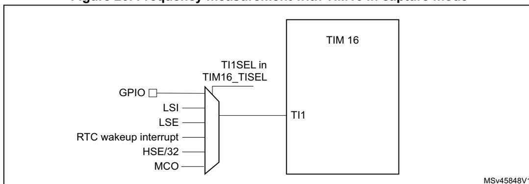
The diagram shows a multiplexer on the left with six inputs: 'GPIO', 'LSI', 'LSE', 'RTC wakeup interrupt', 'HSE/32', and 'MCO'. The output of the multiplexer is connected to the 'TI1' input of a block labeled 'TIM 16'. Above the multiplexer is the label 'TI1SEL in TIM16_TISEL'. In the bottom right corner of the diagram area, the text 'MSV45848V1' is present.
The input capture channel of the Timer 16 can be a GPIO line or an internal clock of the MCU.
The possibilities are the following ones:
- • TIM16 Channel1 is connected to the GPIO. Refer to the alternate function mapping in the device datasheets.
- • TIM16 Channel1 is connected to the LSI clock.
- • TIM16 Channel1 is connected to the LSE clock.
- • TIM16 Channel1 is connected to the RTC wake-up interrupt signal. In this case the RTC interrupt should be enabled.
- • TIM16 Channel1 is connected to the HSE/32 clock.
- • TIM16 Channel1 is connected to the MCO.
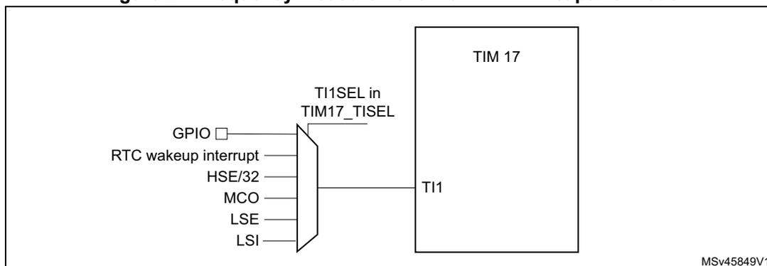
The diagram shows a multiplexer selecting the input for the TIM17 TI1 channel. The multiplexer is controlled by the 'TI1SEL in TIM17_TISEL' register. The input options are:
- GPIO
- RTC wakeup interrupt
- HSE/32
- MCO
- LSE
- LSI
The input capture channel of Timer 17 can be a GPIO line or an internal clock of the MCU.
The possibilities are the following ones:
- • TIM17 Channel1 is connected to the GPIO. Refer to the alternate function mapping in the device datasheets.
- • TIM17 Channel1 is connected to the RTC wake-up interrupt. In this case the RTC interrupt should be enabled.
- • TIM17 Channel1 is connected to the HSE/32 clock.
- • TIM17 Channel1 is connected to the microcontroller clock output (MCO), this selection is controlled by the MCOSEL[3:0] bits of the Clock configuration register (RCC_CFGR) .
- • TIM17 Channel1 is connected to the LSE clock.
- • TIM17 Channel1 is connected to the LSI clock.
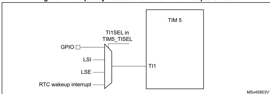
The diagram shows a multiplexer selecting the input for the TIM5 TI1 channel. The multiplexer is controlled by the 'TI1SEL in TIM5_TISEL' register. The input options are:
- GPIO
- LSI
- LSE
- RTC wakeup interrupt
The input capture channel of the Timer 5 can be a GPIO line or an internal clock of the MCU.
The possibilities are the following ones:
- • TIM5 Channel1 is connected to the GPIO. Refer to the alternate function mapping in the device datasheets.
- • TIM5 Channel1 is connected to the LSI clock.
- • TIM5 Channel1 is connected to the LSE clock.
- • TIM5 Channel1 is connected to the RTC wake-up interrupt signal. In this case the RTC interrupt should be enabled.
Calibration of the HSI16
For TIM15 and TIM16, the primary purpose of connecting the LSE to the channel 1 input capture is to be able to precisely measure the HSI16 system clocks (for this, the HSI16 should be used as the system clock source). The number of HSI16 clock counts between consecutive edges of the LSE signal provides a measure of the internal clock period. Taking advantage of the high precision of LSE crystals (typically a few tens of ppm's), it is possible to determine the internal clock frequency with the same resolution, and trim the source to compensate for manufacturing, process, temperature and/or voltage related frequency deviations.
The HSI16 oscillator has dedicated user-accessible calibration bits for this purpose.
The basic concept consists in providing a relative measurement (e.g. the HSI16/LSE ratio): the precision is therefore closely related to the ratio between the two clock sources. The higher the ratio is, the better the measurement is.
If LSE is not available, HSE/32 is the better option in order to reach the most precise calibration possible.
Calibration of the LSI
The calibration of the LSI follows the same pattern that for the HSI16, but changing the reference clock. It is necessary to connect LSI clock to the channel 1 input capture of the TIM16. Then define the HSE as system clock source, the number of his clock counts between consecutive edges of the LSI signal provides a measure of the internal low speed clock period.
The basic concept consists in providing a relative measurement (e.g. the HSE/LSI ratio): the precision is therefore closely related to the ratio between the two clock sources. The higher the ratio is, the better the measurement is.
7.2.17 Peripheral clock enable register
(RCC_AHBxENR, RCC_APBxENRy)
Each peripheral clock can be enabled by the xxxxEN bit of the RCC_AHBxENR, RCC_APBxENRy registers.
When the peripheral clock is not active, the peripheral registers read or write accesses are not supported.
The enable bit has a synchronization mechanism to create a glitch free clock for the peripheral. After the enable bit is set, there is a 2 clock cycles delay before the clock be active.
Caution: Just after enabling the clock for a peripheral, software must wait for a delay before accessing the peripheral registers.
7.3 Low-power modes
- • AHB and APB peripheral clocks, including DMA clock, can be disabled by software.
- • Sleep and Low Power Sleep modes stops the CPU clock. The memory interface clocks (Flash and SRAM1, SRAM2 and CCM SRAM interfaces) can be stopped by software during sleep mode. The AHB to APB bridge clocks are disabled by hardware during Sleep mode when all the clocks of the peripherals connected to them are disabled.
- • Stop modes (Stop 0 and Stop 1) stops all the clocks in the \( V_{\text{CORE}} \) domain and disables the PLL, the HSI16, and the HSE oscillators.
All U(S)ARTs, LPUARTs and \( I^2C \) s have the capability to enable the HSI16 oscillator even when the MCU is in Stop mode (if HSI16 is selected as the clock source for that peripheral).
All U(S)ARTs and LPUARTs can also be driven by the LSE oscillator when the system is in Stop mode (if LSE is selected as clock source for that peripheral) and the LSE oscillator is enabled (LSEON). In that case the LSE remains always ON in Stop mode (they do not have the capability to turn on the LSE oscillator).
- • Standby and Shutdown modes stops all the clocks in the \( V_{\text{CORE}} \) domain and disables the PLL, the HSI16, and the HSE oscillators.
The CPU's deepsleep mode can be overridden for debugging by setting the DBG_STOP or DBG_STANDBY bits in the DBGMCU_CR register.
When leaving the Stop modes (Stop 0, Stop 1 or standby), the system clock is HSI16.
If a Flash memory programming operation is on going, Stop, Standby and Shutdown modes entry is delayed until the Flash memory interface access is finished. If an access to the APB domain is ongoing, Stop, Standby and Shutdown modes entry is delayed until the APB access is finished.
7.4 RCC registers
7.4.1 Clock control register (RCC_CR)
Address offset: 0x00
Reset value: 0x0000 0500
HSEBYP is not affected by reset.
Access: no wait state, word, half-word and byte access
| 31 | 30 | 29 | 28 | 27 | 26 | 25 | 24 | 23 | 22 | 21 | 20 | 19 | 18 | 17 | 16 |
|---|---|---|---|---|---|---|---|---|---|---|---|---|---|---|---|
| Res. | Res. | Res. | Res. | Res. | Res. | PLL RDY | PLLON | Res. | Res. | Res. | Res. | CSSON | HSEBYP | HSERDY | HSEON |
| r | rw | rs | rw | r | rw | ||||||||||
| 15 | 14 | 13 | 12 | 11 | 10 | 9 | 8 | 7 | 6 | 5 | 4 | 3 | 2 | 1 | 0 |
| Res. | Res. | Res. | Res. | Res. | HSI RDY | HSI KERON | HSION | Res. | Res. | Res. | Res. | Res. | Res. | Res. | Res. |
| r | rw | rw |
Bits 31:26 Reserved, must be kept at reset value.
Bit 25 PLLRDY : Main PLL clock ready flag
Set by hardware to indicate that the main PLL is locked.
0: PLL unlocked
1: PLL locked
Bit 24 PLLON : Main PLL enable
Set and cleared by software to enable the main PLL.
Cleared by hardware when entering Stop, Standby or Shutdown mode. This bit cannot be reset if the PLL clock is used as the system clock.
0: PLL OFF
1: PLL ON
Bits 23:20 Reserved, must be kept at reset value.
Bit 19 CSSON : Clock security system enable
Set by software to enable the clock security system. When CSSON is set, the clock detector is enabled by hardware when the HSE oscillator is ready, and disabled by hardware if a HSE clock failure is detected. This bit is set only and is cleared by reset.
0: Clock security system OFF (clock detector OFF)
1: Clock security system ON (Clock detector ON if the HSE oscillator is stable, OFF if not).
Bit 18 HSEBYP : HSE crystal oscillator bypass
Set and cleared by software to bypass the oscillator with an external clock. The external clock must be enabled with the HSEON bit set, to be used by the device. The HSEBYP bit can be written only if the HSE oscillator is disabled.
0: HSE crystal oscillator not bypassed
1: HSE crystal oscillator bypassed with external clock
Bit 17 HSERDY : HSE clock ready flag
Set by hardware to indicate that the HSE oscillator is stable.
0: HSE oscillator not ready
1: HSE oscillator ready
Note: Once the HSEON bit is cleared, HSERDY goes low after 6 HSE clock cycles.
Bit 16 HSEON : HSE clock enable
Set and cleared by software.
Cleared by hardware to stop the HSE oscillator when entering Stop, Standby or Shutdown mode. This bit cannot be reset if the HSE oscillator is used directly or indirectly as the system clock.
0: HSE oscillator OFF
1: HSE oscillator ON
Bits 15:11 Reserved, must be kept at reset value.
Bit 10 HSIRDY : HSI16 clock ready flag
Set by hardware to indicate that HSI16 oscillator is stable. This bit is set only when HSI16 is enabled by software by setting HSION.
0: HSI16 oscillator not ready
1: HSI16 oscillator ready
Note: Once the HSION bit is cleared, HSIRDY goes low after 6 HSI16 clock cycles.
Bit 9 HSIKERON : HSI16 always enable for peripheral kernels.
Set and cleared by software to force HSI16 ON even in Stop modes. The HSI16 can only feed USARTs and I 2 Cs peripherals configured with HSI16 as kernel clock. Keeping the HSI16 ON in Stop mode allows to avoid slowing down the communication speed because of the HSI16 startup time. This bit has no effect on HSION value.
0: No effect on HSI16 oscillator.
1: HSI16 oscillator is forced ON even in Stop mode.
Bit 8 HSION : HSI16 clock enable
Set and cleared by software.
Cleared by hardware to stop the HSI16 oscillator when entering Stop, Standby or Shutdown mode.
Set by hardware to force the HSI16 oscillator ON when STOPWUCK=1 or HSIASFS = 1 when leaving Stop modes, or in case of failure of the HSE crystal oscillator.
This bit is set by hardware if the HSI16 is used directly or indirectly as system clock.
0: HSI16 oscillator OFF
1: HSI16 oscillator ON
Bits 7:0 Reserved, must be kept at reset value.
7.4.2 Internal clock sources calibration register (RCC_ICSCR)
Address offset: 0x04
Reset value: 0x40XX 00XX
where X is factory-programmed.
Access: no wait state, word, half-word and byte access
| 31 | 30 | 29 | 28 | 27 | 26 | 25 | 24 | 23 | 22 | 21 | 20 | 19 | 18 | 17 | 16 |
|---|---|---|---|---|---|---|---|---|---|---|---|---|---|---|---|
| Res. | HSITRIM[6:0] | HSICAL[7:0] | |||||||||||||
| rw | rw | rw | rw | rw | rw | rw | r | r | r | r | r | r | r | r | |
| 15 | 14 | 13 | 12 | 11 | 10 | 9 | 8 | 7 | 6 | 5 | 4 | 3 | 2 | 1 | 0 |
| Res. | Res. | Res. | Res. | Res. | Res. | Res. | Res. | Res. | Res. | Res. | Res. | Res. | Res. | Res. | Res. |
Bit 31 Reserved, must be kept at reset value.
Bits 30:24 HSITRIM[6:0] : HSI16 clock trimming
These bits provide an additional user-programmable trimming value that is added to the HSICAL[7:0] bits. It can be programmed to adjust to variations in voltage and temperature that influence the frequency of the HSI16.
The default value is 64, which, when added to the HSICAL value, trims HSI16 to 16 MHz \( \pm \) 1 %.
Bits 23:16 HSICAL[7:0] : HSI16 clock calibration
These bits are initialized at startup with the factory-programmed HSI16 calibration trim value. When HSITRIM is written, HSICAL is updated with the sum of HSITRIM and the factory trim value.
Bits 15:0 Reserved, must be kept at reset value.
7.4.3 Clock configuration register (RCC_CFGR)
Address offset: 0x08
Reset value: 0x0000 0005
Access: 0 \( \leq \) wait state \( \leq \) 2, word, half-word and byte access
1 or 2 wait states inserted only if the access occurs during clock source switch.
From 0 to 15 wait states inserted if the access occurs when the APB or AHB prescalers values update is on going.
| 31 | 30 | 29 | 28 | 27 | 26 | 25 | 24 | 23 | 22 | 21 | 20 | 19 | 18 | 17 | 16 |
|---|---|---|---|---|---|---|---|---|---|---|---|---|---|---|---|
| Res. | MCOPRE[2:0] | MCOSEL[3:0] | Res. | Res. | Res. | Res. | Res. | Res. | Res. | Res. | |||||
| rw | rw | rw | rw | rw | rw | rw | |||||||||
| 15 | 14 | 13 | 12 | 11 | 10 | 9 | 8 | 7 | 6 | 5 | 4 | 3 | 2 | 1 | 0 |
| Res. | Res. | PPRE2[2:0] | PPRE1[2:0] | HPRE[3:0] | SWS[1:0] | SW[1:0] | |||||||||
| rw | rw | rw | rw | rw | rw | rw | rw | rw | rw | r | r | rw | rw | ||
Bit 31 Reserved, must be kept at reset value.
Bits 30:28 MCOPRE[2:0] : Microcontroller clock output prescaler
These bits are set and cleared by software.
It is highly recommended to change this prescaler before MCO output is enabled.
000: MCO is divided by 1
001: MCO is divided by 2
010: MCO is divided by 4
011: MCO is divided by 8
100: MCO is divided by 16
Others: not allowed
Bits 27:24 MCOSEL[3:0] : Microcontroller clock output
Set and cleared by software.
0000: MCO output disabled, no clock on MCO
0001: SYSCLK system clock selected
0010: Reserved, must be kept at reset value
0011: HSI16 clock selected
0100: HSE clock selected
0101: Main PLL clock selected
0110: LSI clock selected
0111: LSE clock selected
1000: Internal HSI48 clock selected
Others: Reserved
Note: This clock output may have some truncated cycles at startup or during MCO clock source switching.
Bits 23:14 Reserved, must be kept at reset value.
Bits 13:11 PPRE2[2:0] : APB2 prescaler
Set and cleared by software to control the division factor of the APB2 clock (PCLK2).
0xx: HCLK not divided
100: HCLK divided by 2
101: HCLK divided by 4
110: HCLK divided by 8
111: HCLK divided by 16
Bits 10:8 PPRE1[2:0] : APB1 prescaler
Set and cleared by software to control the division factor of the APB1 clock (PCLK1).
0xx: HCLK not divided
100: HCLK divided by 2
101: HCLK divided by 4
110: HCLK divided by 8
111: HCLK divided by 16
Bits 7:4 HPRE[3:0] : AHB prescaler
Set and cleared by software to control the division factor of the AHB clock.
Caution: Depending on the device voltage range, the software must set correctly these bits to ensure that the system frequency does not exceed the maximum allowed frequency (for more details refer to Section 6.1.5: Dynamic voltage scaling management ). After a write operation to these bits and before decreasing the voltage range, this register must be read to be sure that the new value has been taken into account.
0xxx: SYSCLK not divided
1000: SYSCLK divided by 2
1001: SYSCLK divided by 4
1010: SYSCLK divided by 8
1011: SYSCLK divided by 16
1100: SYSCLK divided by 64
1101: SYSCLK divided by 128
1110: SYSCLK divided by 256
1111: SYSCLK divided by 512
Bits 3:2 SWS[1:0] : System clock switch status
Set and cleared by hardware to indicate which clock source is used as system clock.
00: Reserved, must be kept at reset value
01: HSI16 oscillator used as system clock
10: HSE used as system clock
11: PLL used as system clock
Bits 1:0 SW[1:0] : System clock switch
Set and cleared by software to select system clock source (SYSCLK).
Configured by hardware to force HSI16 oscillator selection when exiting Stop and Standby modes or in case of failure of the HSE oscillator.
00: Reserved, must be kept at reset value
01: HSI16 selected as system clock
10: HSE selected as system clock
11: PLL selected as system clock
7.4.4 PLL configuration register (RCC_PLLCFGR)
Address offset: 0x0C
Reset value: 0x0000 1000
Access: no wait state, word, half-word and byte access
This register is used to configure the PLL clock outputs according to the formulas:
- • \( f(\text{VCO clock}) = f(\text{PLL clock input}) \times (\text{PLLN} / \text{PLLM}) \)
- • \( f(\text{PLL\_P}) = f(\text{VCO clock}) / \text{PLLP} \)
- • \( f(\text{PLL\_Q}) = f(\text{VCO clock}) / \text{PLLQ} \)
- • \( f(\text{PLL\_R}) = f(\text{VCO clock}) / \text{PLLR} \)
| 31 | 30 | 29 | 28 | 27 | 26 | 25 | 24 | 23 | 22 | 21 | 20 | 19 | 18 | 17 | 16 |
|---|---|---|---|---|---|---|---|---|---|---|---|---|---|---|---|
| PLLPDIV[4:0] | PLLR[1:0] | PLL REN | Res. | PLLQ[1:0] | PLL QEN | Res. | Res. | PLLP | PLL PEN | ||||||
| rw | rw | rw | rw | rw | rw | rw | rw | rw | rw | rw | rw | rw | |||
| 15 | 14 | 13 | 12 | 11 | 10 | 9 | 8 | 7 | 6 | 5 | 4 | 3 | 2 | 1 | 0 |
| Res. | PLLN[6:0] | PLLM[3:0] | Res. | Res. | PLLSRC[1:0] | ||||||||||
| rw | rw | rw | rw | rw | rw | rw | rw | rw | rw | rw | rw | rw | |||
Bits 31:27 PLLPDIV[4:0] : Main PLLP division factor
Set and cleared by software to control the PLL ‘P’ frequency. PLL ‘P’ output clock frequency = VCO frequency / PLLPDIV.
00000: PLL ‘P’ clock is controlled by the bit PLLP
00001: Reserved.
00010: PLL ‘P’ clock = VCO / 2
....
11111: PLL ‘P’ clock = VCO / 31
Bits 26:25 PLL[R1:0] : Main PLL division factor for PLL “R” clock (system clock)
Set and cleared by software to control the frequency of the main PLL output clock PLLCLK. This output can be selected as system clock. These bits can be written only if PLL is disabled.
PLL “R” output clock frequency = VCO frequency / PLLR with PLLR = 2, 4, 6, or 8
00: PLLR = 2
01: PLLR = 4
10: PLLR = 6
11: PLLR = 8
Caution: These bits must be set so as not to exceed 170 MHz on this domain.
Bit 24 PLLREN : PLL “R” clock output enable
Set and reset by software to enable the PLL “R” clock output of the PLL (used as system clock).
This bit cannot be written when PLL “R” clock output of the PLL is used as System Clock. In order to save power, when the PLL “R” clock output of the PLL is not used, the value of PLLREN should be 0.
0: PLL “R” clock output disabled
1: PLL “R” clock output enabled
Bit 23 Reserved, must be kept at reset value.
Bits 22:21 PLLQ[1:0] : Main PLL division factor for PLL “Q” clock.
Set and cleared by software to control the frequency of the main PLL output clock PLL “Q” clock. This output can be selected for USB, RNG, SAI (48 MHz clock). These bits can be written only if PLL is disabled.
PLL “Q” output clock frequency = VCO frequency / PLLQ with PLLQ = 2, 4, 6, or 8
00: PLLQ = 2
01: PLLQ = 4
10: PLLQ = 6
11: PLLQ = 8
Caution: These bits must be set so as not to exceed 170 MHz on this domain.
Bit 20 PLLQEN : Main PLL “Q” clock output enable
Set and reset by software to enable the PLL “Q” clock output of the PLL.
In order to save power, when the PLL “Q” clock output of the PLL is not used, the value of PLLQEN should be 0.
0: PLL “Q” clock output disabled
1: PLL “Q” clock output enabled
Bits 19:18 Reserved, must be kept at reset value.
Bit 17 PLLP : Main PLL division factor for PLL “P” clock.
Set and cleared by software to control the frequency of the main PLL output clock PLL “P” clock. These bits can be written only if PLL is disabled.
When the PLLPDIV[4:0] is set to “00000” PLL “P” output clock frequency = VCO frequency / PLLP with PLLP = 7, or 17
0: PLLP = 7
1: PLLP = 17
Caution: These bits must be set so as not to exceed 170 MHz on this domain.
Bit 16 PLLPEN : Main PLL PLL “P” clock output enable
Set and reset by software to enable the PLL “P” clock output of the PLL.
To save power, when the PLL “P” clock output of the PLL is not used, the value of PLLPEN should be 0.
0: PLL “P” clock output disabled
1: PLL “P” clock output enabled
Bit 15 Reserved, must be kept at reset value.
Bits 14:8 PLLN[6:0] : Main PLL multiplication factor for VCO
Set and cleared by software to control the multiplication factor of the VCO. These bits can be written only when the PLL is disabled.
VCO output frequency = VCO input frequency x PLLN with \( 8 \leq PLLN \leq 127 \)
0000000: PLLN = 0 wrong configuration
0000001: PLLN = 1 wrong configuration
...
0000111: PLLN = 7 wrong configuration
0001000: PLLN = 8
0001001: PLLN = 9
...
1111111: PLLN = 127
Caution: The software must set correctly these bits to assure that the VCO output frequency is within the range defined in the datasheet.
Bits 7:4 PLLM[3:0] : Division factor for the main PLL input clock
Set and cleared by software to divide the PLL input clock before the VCO. These bits can be written only when all PLLs are disabled.
VCO input frequency = PLL input clock frequency / PLLM with \( 1 \leq PLLM \leq 16 \)
0000: PLLM = 1
0001: PLLM = 2
0010: PLLM = 3
0011: PLLM = 4
0100: PLLM = 5
0101: PLLM = 6
0110: PLLM = 7
0111: PLLM = 8
1000: PLLSYSM = 9
...
1111: PLLSYSM= 16
Caution: The software must set these bits correctly to ensure that the VCO input frequency is within the range defined in the datasheet.
Bits 3:2 Reserved, must be kept at reset value.
Bits 1:0 PLL SRC[1:0] : Main PLL entry clock source
Set and cleared by software to select PLL clock source. These bits can be written only when PLL is disabled.
In order to save power, when no PLL is used, the value of PLLSRC should be 00.
00: No clock sent to PLL
01: No clock sent to PLL
10: HSI16 clock selected as PLL clock entry
11: HSE clock selected as PLL clock entry
7.4.5 Clock interrupt enable register (RCC_CIER)
Address offset: 0x18
Reset value: 0x0000 0000
Access: no wait state, word, half-word and byte access
| 31 | 30 | 29 | 28 | 27 | 26 | 25 | 24 | 23 | 22 | 21 | 20 | 19 | 18 | 17 | 16 |
|---|---|---|---|---|---|---|---|---|---|---|---|---|---|---|---|
| Res. | Res. | Res. | Res. | Res. | Res. | Res. | Res. | Res. | Res. | Res. | Res. | Res. | Res. | Res. | Res. |
| 15 | 14 | 13 | 12 | 11 | 10 | 9 | 8 | 7 | 6 | 5 | 4 | 3 | 2 | 1 | 0 |
| Res. | Res. | Res. | Res. | Res. | HSI48 RDYIE | LSE CSSIE | Res. | Res. | Res. | PLL RDYIE | HSE RDYIE | HSI RDYIE | Res. | LSE RDYIE | LSI RDYIE |
| rw | rw | rw | rw | rw | rw | rw |
Bits 31:11 Reserved, must be kept at reset value.
Bit 10 HSI48RDYIE : HSI48 ready interrupt enable
Set and cleared by software to enable/disable interrupt caused by the internal HSI48 oscillator.
0: HSI48 ready interrupt disabled
1: HSI48 ready interrupt enabled
Bit 9 LSECSSIE : LSE clock security system interrupt enable
Set and cleared by software to enable/disable interrupt caused by the clock security system on LSE.
0: Clock security interrupt caused by LSE clock failure disabled
1: Clock security interrupt caused by LSE clock failure enabled
Bits 8:6 Reserved, must be kept at reset value.
Bit 5 PLLRDYIE : PLL ready interrupt enable
Set and cleared by software to enable/disable interrupt caused by PLL lock.
0: PLL lock interrupt disabled
1: PLL lock interrupt enabled
Bit 4 HSERDYIE : HSE ready interrupt enable
Set and cleared by software to enable/disable interrupt caused by the HSE oscillator stabilization.
0: HSE ready interrupt disabled
1: HSE ready interrupt enabled
Bit 3 HSIRDYIE : HSI16 ready interrupt enable
Set and cleared by software to enable/disable interrupt caused by the HSI16 oscillator stabilization.
0: HSI16 ready interrupt disabled
1: HSI16 ready interrupt enabled
Bit 2 Reserved, must be kept at reset value.
Bit 1 LSERDYIE : LSE ready interrupt enable
Set and cleared by software to enable/disable interrupt caused by the LSE oscillator stabilization.
0: LSE ready interrupt disabled
1: LSE ready interrupt enabled
Bit 0 LSIRDYIE : LSI ready interrupt enable
Set and cleared by software to enable/disable interrupt caused by the LSI oscillator stabilization.
0: LSI ready interrupt disabled
1: LSI ready interrupt enabled
7.4.6 Clock interrupt flag register (RCC_CIFR)
Address offset: 0x1C
Reset value: 0x0000 0000
Access: no wait state, word, half-word and byte access
| 31 | 30 | 29 | 28 | 27 | 26 | 25 | 24 | 23 | 22 | 21 | 20 | 19 | 18 | 17 | 16 |
|---|---|---|---|---|---|---|---|---|---|---|---|---|---|---|---|
| Res. | Res. | Res. | Res. | Res. | Res. | Res. | Res. | Res. | Res. | Res. | Res. | Res. | Res. | Res. | Res. |
| 15 | 14 | 13 | 12 | 11 | 10 | 9 | 8 | 7 | 6 | 5 | 4 | 3 | 2 | 1 | 0 |
| Res. | Res. | Res. | Res. | Res. | HSI48 RDYF | LSE CSSF | CSSF | Res. | Res. | PLL RDYF | HSE RDYF | HSI RDYF | Res. | LSE RDYF | LSI RDYF |
| r | r | r | r | r | r | r | r |
Bits 31:11 Reserved, must be kept at reset value.
Bit 10 HSI48RDYF : HSI48 ready interrupt flag
Set by hardware when the HSI48 clock becomes stable and HSI48RDYIE is set in a response to setting the HSI48ON (refer to Clock recovery RC register (RCC_CRRCR) ).
Cleared by software setting the HSI48RDYC bit.
0: No clock ready interrupt caused by the HSI48 oscillator
1: Clock ready interrupt caused by the HSI48 oscillator
Bit 9 LSECSSF : LSE clock security system interrupt flag
Set by hardware when a failure is detected in the LSE oscillator.
Cleared by software setting the LSECSSC bit.
0: No clock security interrupt caused by LSE clock failure
1: Clock security interrupt caused by LSE clock failure
Bit 8 CSSF : Clock security system interrupt flag
Set by hardware when a failure is detected in the HSE oscillator.
Cleared by software setting the CSSC bit.
0: No clock security interrupt caused by HSE clock failure
1: Clock security interrupt caused by HSE clock failure
Bits 7:6 Reserved, must be kept at reset value.
Bit 5 PLLRDYF : PLL ready interrupt flag
Set by hardware when the PLL locks and PLLRDYIE is set.
Cleared by software setting the PLLRDYC bit.
0: No clock ready interrupt caused by PLL lock
1: Clock ready interrupt caused by PLL lock
Bit 4 HSERDYF : HSE ready interrupt flag
Set by hardware when the HSE clock becomes stable and HSERDYIE is set.
Cleared by software setting the HSERDYC bit.
0: No clock ready interrupt caused by the HSE oscillator
1: Clock ready interrupt caused by the HSE oscillator
Bit 3 HSIRDYF : HSI16 ready interrupt flag
Set by hardware when the HSI16 clock becomes stable and HSIRDYIE is set in a response to setting the HSION (refer to Clock control register (RCC_CR) ). When HSION is not set but the HSI16 oscillator is enabled by the peripheral through a clock request, this bit is not set and no interrupt is generated.
Cleared by software setting the HSIRDYC bit.
0: No clock ready interrupt caused by the HSI16 oscillator
1: Clock ready interrupt caused by the HSI16 oscillator
Bit 2 Reserved, must be kept at reset value.
Bit 1 LSERDYF : LSE ready interrupt flag
Set by hardware when the LSE clock becomes stable and LSERDYIE is set.
Cleared by software setting the LSERDYC bit.
0: No clock ready interrupt caused by the LSE oscillator
1: Clock ready interrupt caused by the LSE oscillator
Bit 0 LSIRDYF : LSI ready interrupt flag
Set by hardware when the LSI clock becomes stable and LSIRDYIE is set.
Cleared by software setting the LSIRDYC bit.
0: No clock ready interrupt caused by the LSI oscillator
1: Clock ready interrupt caused by the LSI oscillator
7.4.7 Clock interrupt clear register (RCC_CICR)
Address offset: 0x20
Reset value: 0x0000 0000
Access: no wait state, word, half-word and byte access
| 31 | 30 | 29 | 28 | 27 | 26 | 25 | 24 | 23 | 22 | 21 | 20 | 19 | 18 | 17 | 16 |
|---|---|---|---|---|---|---|---|---|---|---|---|---|---|---|---|
| Res. | Res. | Res. | Res. | Res. | Res. | Res. | Res. | Res. | Res. | Res. | Res. | Res. | Res. | Res. | Res. |
| 15 | 14 | 13 | 12 | 11 | 10 | 9 | 8 | 7 | 6 | 5 | 4 | 3 | 2 | 1 | 0 |
| Res. | Res. | Res. | Res. | Res. | HSI48 RDYC | LSE CSSC | CSSC | Res. | Res. | PLL RDYC | HSE RDYC | HSI RDYC | Res. | LSE RDYC | LSI RDYC |
| w | w | w | w | w | w | w | w |
Bits 31:11 Reserved, must be kept at reset value.
Bit 10 HSI48RDYC : HSI48 oscillator ready interrupt clear
This bit is set by software to clear the HSI48RDYF flag.
0: No effect
1: Clear the HSI48RDYC flag
Bit 9
LSECSSC
: LSE clock security system interrupt clear
This bit is set by software to clear the LSECSSF flag.
0: No effect
1: Clear LSECSSF flag
Bit 8
CSSC
: Clock security system interrupt clear
This bit is set by software to clear the CSSF flag.
0: No effect
1: Clear CSSF flag
Bits 7:6 Reserved, must be kept at reset value.
Bit 5
PLLRDYC
: PLL ready interrupt clear
This bit is set by software to clear the PLLRDYF flag.
0: No effect
1: Clear PLLRDYF flag
Bit 4
HSERDYC
: HSE ready interrupt clear
This bit is set by software to clear the HSERDYF flag.
0: No effect
1: Clear HSERDYF flag
Bit 3
HSIRDYC
: HSI16 ready interrupt clear
This bit is set software to clear the HSIRDYF flag.
0: No effect
1: Clear HSIRDYF flag
Bit 2 Reserved, must be kept at reset value.
Bit 1
LSERDYC
: LSE ready interrupt clear
This bit is set by software to clear the LSERDYF flag.
0: No effect
1: LSERDYF cleared
Bit 0
LSIRDYC
: LSI ready interrupt clear
This bit is set by software to clear the LSIRDYF flag.
0: No effect
1: LSIRDYF cleared
7.4.8 AHB1 peripheral reset register (RCC_AHB1RSTR)
Address offset: 0x28
Reset value: 0x0000 0000
Access: no wait state, word, half-word and byte access
| 31 | 30 | 29 | 28 | 27 | 26 | 25 | 24 | 23 | 22 | 21 | 20 | 19 | 18 | 17 | 16 |
|---|---|---|---|---|---|---|---|---|---|---|---|---|---|---|---|
| Res. | Res. | Res. | Res. | Res. | Res. | Res. | Res. | Res. | Res. | Res. | Res. | Res. | Res. | Res. | Res. |
| 15 | 14 | 13 | 12 | 11 | 10 | 9 | 8 | 7 | 6 | 5 | 4 | 3 | 2 | 1 | 0 |
| Res. | Res. | Res. | CRC RST | Res. | Res. | Res. | FLASH RST | Res. | Res. | Res. | FMAC RST | CORDIC RST | DMAMUX1 RST | DMA2 RST | DMA1 RST |
| rw | rw | rw | rw | rw | rw | rw |
Bits 31:13 Reserved, must be kept at reset value.
Bit 12 CRCRST : CRC reset
Set and cleared by software.
0: No effect
1: Reset CRC
Bits 11:9 Reserved, must be kept at reset value.
Bit 8 FLASHRST : Flash memory interface reset
Set and cleared by software. This bit can be activated only when the Flash memory is in power down mode.
0: No effect
1: Reset Flash memory interface
Bits 7:5 Reserved, must be kept at reset value.
Bit 4 FMACRST : Set and cleared by software
0: No effect
1: Reset FMAC
Bit 3 CORDICRST : Set and cleared by software
0: No effect
1: Reset CORDIC
Bit 2 DMAMUX1RST : Set and cleared by software.
0: No effect
1: Reset DMAMUX1
Bit 1 DMA2RST : DMA2 reset
Set and cleared by software.
0: No effect
1: Reset DMA2
Bit 0 DMA1RST : DMA1 reset
Set and cleared by software.
0: No effect
1: Reset DMA1
7.4.9 AHB2 peripheral reset register (RCC_AHB2RSTR)
Address offset: 0x2C
Reset value: 0x0000 0000
Access: no wait state, word, half-word and byte access
| 31 | 30 | 29 | 28 | 27 | 26 | 25 | 24 | 23 | 22 | 21 | 20 | 19 | 18 | 17 | 16 |
|---|---|---|---|---|---|---|---|---|---|---|---|---|---|---|---|
| Res. | Res. | Res. | Res. | Res. | RNG RST | Res. | AES RST | Res. | Res. | Res. | Res. | DAC4 RST | DAC3 RST | DAC2 RST | DAC1 RST |
| rw | rw | rw | rw | rw | rw | ||||||||||
| 15 | 14 | 13 | 12 | 11 | 10 | 9 | 8 | 7 | 6 | 5 | 4 | 3 | 2 | 1 | 0 |
| Res. | ADC345 RST | ADC12 RST | Res. | Res. | Res. | Res. | Res. | Res. | GPIOG RST | GPIOF RST | GPIOE RST | GPIO D RST | GPIOC RST | GPIOB RST | GPIOA RST |
| rw | rw | rw | rw | rw | rw | rw | rw | rw |
Bits 31:27 Reserved, must be kept at reset value.
Bit 26
RNGRST
: RNG reset
Set and cleared by software.
0: No effect
1: Reset RNG
Bit 25 Reserved, must be kept at reset value.
Bit 24
AESRST
: AESRST reset
Set and cleared by software.
0: No effect
1: Reset AES
Bits 23:20 Reserved, must be kept at reset value.
Bit 19
DAC4RST
: DAC4 reset
Set and cleared by software.
0: No effect
1: Reset DAC4
Bit 18
DAC3RST
: DAC3 reset
Set and cleared by software.
0: No effect
1: Reset DAC3
Bit 17
DAC2RST
: DAC2 reset
Set and cleared by software.
0: No effect
1: Reset DAC2
Bit 16
DAC1RST
: DAC1 reset
Set and cleared by software.
0: No effect
1: Reset DAC1
Bit 15 Reserved, must be kept at reset value.
Bit 14
ADC345RST
: ADC345 reset
Set and cleared by software.
0: No effect
1: Reset ADC345
Bit 13
ADC12RST
: ADC12 reset
Set and cleared by software.
0: No effect
1: Reset ADC12 interface
Bits 12:7 Reserved, must be kept at reset value.
Bit 6
GPIORST
: IO port G reset
Set and cleared by software.
0: No effect
1: Reset IO port G
Bit 5
GPIOFRST
: IO port F reset
Set and cleared by software.
0: No effect
1: Reset IO port F
- Bit 4
GPIOERST
: IO port E reset
Set and cleared by software.
0: No effect
1: Reset IO port E - Bit 3
GIODRST
: IO port D reset
Set and cleared by software.
0: No effect
1: Reset IO port D - Bit 2
GPIOCRST
: IO port C reset
Set and cleared by software.
0: No effect
1: Reset IO port C - Bit 1
GPIOBRST
: IO port B reset
Set and cleared by software.
0: No effect
1: Reset IO port B - Bit 0
GPIOARST
: IO port A reset
Set and cleared by software.
0: No effect
1: Reset IO port A
7.4.10 AHB3 peripheral reset register (RCC_AHB3RSTR)
Address offset: 0x30
Reset value: 0x0000 0000
Access: no wait state, word, half-word and byte access
| 31 | 30 | 29 | 28 | 27 | 26 | 25 | 24 | 23 | 22 | 21 | 20 | 19 | 18 | 17 | 16 |
|---|---|---|---|---|---|---|---|---|---|---|---|---|---|---|---|
| Res. | Res. | Res. | Res. | Res. | Res. | Res. | Res. | Res. | Res. | Res. | Res. | Res. | Res. | Res. | Res. |
| 15 | 14 | 13 | 12 | 11 | 10 | 9 | 8 | 7 | 6 | 5 | 4 | 3 | 2 | 1 | 0 |
| Res. | Res. | Res. | Res. | Res. | Res. | Res. | QSPIRST | Res. | Res. | Res. | Res. | Res. | Res. | Res. | FMC RST |
| rw | rw |
Bits 31:9 Reserved, must be kept at reset value.
- Bit 8
QSPIRST
: QUADSPI reset
Set and cleared by software.
0: No effect
1: Reset QUADSPI
Bits 7:1 Reserved, must be kept at reset value.
- Bit 0
FMCRST
: Flexible static memory controller reset
Set and cleared by software.
0: No effect
1: Reset FSMC
7.4.11 APB1 peripheral reset register 1 (RCC_APB1RSTR1)
Address offset: 0x38
Reset value: 0x0000 0000
Access: no wait state, word, half-word and byte access
| 31 | 30 | 29 | 28 | 27 | 26 | 25 | 24 | 23 | 22 | 21 | 20 | 19 | 18 | 17 | 16 |
|---|---|---|---|---|---|---|---|---|---|---|---|---|---|---|---|
| LPTIM1 RST | I2C3 RST | Res. | PWR RST | Res. | Res. | FDCAN RST | Res. | USB RST | I2C2 RST | I2C1 RST | UART5 RST | UART4 RST | USART3 RST | USART2 RST | Res. |
| rw | rw | rw | rw | rw | rw | rw | rw | rw | rw | rw | |||||
| 15 | 14 | 13 | 12 | 11 | 10 | 9 | 8 | 7 | 6 | 5 | 4 | 3 | 2 | 1 | 0 |
| SPI3 RST | SPI2 RST | Res. | Res. | Res. | Res. | Res. | CRS RST | Res. | Res. | TIM7 RST | TIM6 RST | TIM5 RST | TIM4 RST | TIM3 RST | TIM2 RST |
| rw | rw | rw | rw | rw | rw | rw | rw | rw |
Bit 31 LPTIM1RST : Low Power Timer 1 reset
Set and cleared by software.
0: No effect
1: Reset LPTIM1
Bit 30 I2C3RST : I2C3 reset
Set and cleared by software.
0: No effect
1: Reset I2C3 interface
Bit 29 Reserved, must be kept at reset value.
Bit 28 PWRRST : Power interface reset
Set and cleared by software.
0: No effect
1: Reset PWR
Bits 27:26 Reserved, must be kept at reset value.
Bit 25 FDCANRST : FDCAN reset
Set and reset by software.
0: No effect
1: Reset the FDCAN
Bit 24 Reserved, must be kept at reset value.
Bit 23 USBRRST : USB device reset
Set and reset by software.
0: No effect
1: Reset USB device
Bit 22 I2C2RST : I2C2 reset
Set and cleared by software.
0: No effect
1: Reset I2C2
Bit 21 I2C1RST : I2C1 reset
Set and cleared by software.
0: No effect
1: Reset I2C1
Bit 20
UART5RST
: UART5 reset
Set and cleared by software.
0: No effect
1: Reset UART5
Bit 19
UART4RST
: UART4 reset
Set and cleared by software.
0: No effect
1: Reset UART4
Bit 18
USART3RST
: USART3 reset
Set and cleared by software.
0: No effect
1: Reset USART3
Bit 17
USART2RST
: USART2 reset
Set and cleared by software.
0: No effect
1: Reset USART2
Bit 16 Reserved, must be kept at reset value.
Bit 15
SPI3RST
: SPI3 reset
Set and cleared by software.
0: No effect
1: Reset SPI3
Bit 14
SPI2RST
: SPI2 reset
Set and cleared by software.
0: No effect
1: Reset SPI2
Bits 13:9 Reserved, must be kept at reset value.
Bit 8
CRSRST
: CRS reset
Set and cleared by software.
0: No effect
1: Reset CRS
Bits 7:6 Reserved, must be kept at reset value.
Bit 5
TIM7RST
: TIM7 timer reset
Set and cleared by software.
0: No effect
1: Reset TIM7
Bit 4
TIM6RST
: TIM6 timer reset
Set and cleared by software.
0: No effect
1: Reset TIM7
Bit 3
TIM5RST
: TIM5 timer reset
Set and cleared by software.
0: No effect
1: Reset TIM5
- Bit 2
TIM4RST
: TIM3 timer reset
Set and cleared by software.
0: No effect
1: Reset TIM3 - Bit 1
TIM3RST
: TIM3 timer reset
Set and cleared by software.
0: No effect
1: Reset TIM3 - Bit 0
TIM2RST
: TIM2 timer reset
Set and cleared by software.
0: No effect
1: Reset TIM2
7.4.12 APB1 peripheral reset register 2 (RCC_APB1RSTR2)
Address offset: 0x3C
Reset value: 0x0000 0000
Access: no wait state, word, half-word and byte access
| 31 | 30 | 29 | 28 | 27 | 26 | 25 | 24 | 23 | 22 | 21 | 20 | 19 | 18 | 17 | 16 |
|---|---|---|---|---|---|---|---|---|---|---|---|---|---|---|---|
| Res. | Res. | Res. | Res. | Res. | Res. | Res. | Res. | Res. | Res. | Res. | Res. | Res. | Res. | Res. | Res. |
| 15 | 14 | 13 | 12 | 11 | 10 | 9 | 8 | 7 | 6 | 5 | 4 | 3 | 2 | 1 | 0 |
| Res. | Res. | Res. | Res. | Res. | Res. | Res. | UCPD1 RST | Res. | Res. | Res. | Res. | Res. | Res. | I2C4 RST | LPUART1 RST |
| rw | rw | rw |
Bits 31:9 Reserved, must be kept at reset value.
- Bit 8
UCPD1RST
: UCPD1 reset
Set and cleared by software.
0: No effect
1: Reset UCPD1
Bits 7:2 Reserved, must be kept at reset value.
- Bit 1
I2C4RST
: I2C4 reset
Set and cleared by software
0: No effect
1: Reset I2C4
- Bit 0
LPUART1RST
: Low-power UART 1 reset
Set and cleared by software.
0: No effect
1: Reset LPUART1
7.4.13 APB2 peripheral reset register (RCC_APB2RSTR)
Address offset: 0x40
Reset value: 0x0000 0000
Access: no wait state, word, half-word and byte access
| 31 | 30 | 29 | 28 | 27 | 26 | 25 | 24 | 23 | 22 | 21 | 20 | 19 | 18 | 17 | 16 |
|---|---|---|---|---|---|---|---|---|---|---|---|---|---|---|---|
| Res. | Res. | Res. | Res. | Res. | HRTIM1 RST | Res. | Res. | Res. | Res. | SAI1 RST | TIM20 RST | Res. | TIM17 RST | TIM16 RST | TIM15 RST |
| rw | rw | rw | rw | rw | rw | ||||||||||
| 15 | 14 | 13 | 12 | 11 | 10 | 9 | 8 | 7 | 6 | 5 | 4 | 3 | 2 | 1 | 0 |
| SPI4 RST | USART1 RST | TIM8 RST | SPI1 RST | TIM1 RST | Res. | Res. | Res. | Res. | Res. | Res. | Res. | Res. | Res. | Res. | SYSCFG RST |
| rw | rw | rw | rw | rw | rw |
Bits 31:27 Reserved, must be kept at reset value.
Bit 26 HRTIM1RST : HRTIM1 reset
Set and cleared by software.
0: No effect
1: Reset HRTIM1
Bits 25:22 Reserved, must be kept at reset value.
Bit 21 SAI1RST : Serial audio interface 1 (SAI1) reset
Set and cleared by software.
0: No effect
1: Reset SAI1
Bit 20 TIM20RST : TIM20 reset
Set and cleared by software.
0: No effect
1: Reset TIM20
Bit 19 Reserved, must be kept at reset value.
Bit 18 TIM17RST : TIM17 timer reset
Set and cleared by software.
0: No effect
1: Reset TIM17 timer
Bit 17 TIM16RST : TIM16 timer reset
Set and cleared by software.
0: No effect
1: Reset TIM16 timer
Bit 16 TIM15RST : TIM15 timer reset
Set and cleared by software.
0: No effect
1: Reset TIM15 timer
Bit 15 SPI4RST : SPI4 reset
Set and cleared by software.
0: No effect
1: Reset SPI4
Bit 14 USART1RST : USART1 reset
Set and cleared by software.
0: No effect
1: Reset USART1
Bit 13
TIM8RST
: TIM8 timer reset
Set and cleared by software.
0: No effect
1: Reset TIM8 timer
Bit 12
SPI1RST
: SPI1 reset
Set and cleared by software.
0: No effect
1: Reset SPI1
Bit 11
TIM1RST
: TIM1 timer reset
Set and cleared by software.
0: No effect
1: Reset TIM1 timer
Bits 10:1 Reserved, must be kept at reset value.
Bit 0 SYSCFGRST : SYSCFG + COMP + OPAMP + VREFBUF reset
0: No effect
1: Reset SYSCFG + COMP + OPAMP + VREFBUF
7.4.14 AHB1 peripheral clock enable register (RCC_AHB1ENR)
Address offset: 0x48
Reset value: 0x0000 0100
Access: no wait state, word, half-word and byte access
Note: When the peripheral clock is not active, the peripheral registers read or write access is not supported.
| 31 | 30 | 29 | 28 | 27 | 26 | 25 | 24 | 23 | 22 | 21 | 20 | 19 | 18 | 17 | 16 |
|---|---|---|---|---|---|---|---|---|---|---|---|---|---|---|---|
| Res. | Res. | Res. | Res. | Res. | Res. | Res. | Res. | Res. | Res. | Res. | Res. | Res. | Res. | Res. | Res. |
| 15 | 14 | 13 | 12 | 11 | 10 | 9 | 8 | 7 | 6 | 5 | 4 | 3 | 2 | 1 | 0 |
| Res. | Res. | Res. | CRC EN | Res. | Res. | Res. | FLASH EN | Res. | Res. | Res. | FMAC EN | CORDIC EN | DMAMUX1 EN | DMA2 EN | DMA1 EN |
| rw | rw | rw | rw | rw | rw | rw |
Bits 31:13 Reserved, must be kept at reset value.
Bit 12
CRCEN
: CRC clock enable
Set and cleared by software.
0: CRC clock disabled
1: CRC clock enable
Bits 11:9 Reserved, must be kept at reset value.
Bit 8
FLASHEN
: Flash memory interface clock enable
Set and cleared by software. This bit can be disabled only when the Flash is in power down mode.
0: Flash memory interface clock disabled
1: Flash memory interface clock enabled
Bits 7:5 Reserved, must be kept at reset value.
- Bit 4
FMACEN
: FMAC enable
Set and reset by software.
0: FMAC clock disabled
1: FMAC clock enabled - Bit 3
CORDICEN
: CORDIC clock enable
Set and reset by software.
0: CORDIC clock disabled
1: CORDIC clock enabled - Bit 2
DMAMUX1EN
: DMAMUX1 clock enable
Set and reset by software.
0: DMAMUX1 clock disabled
1: DMAMUX1 clock enabled - Bit 1
DMA2EN
: DMA2 clock enable
Set and cleared by software.
0: DMA2 clock disabled
1: DMA2 clock enable - Bit 0
DMA1EN
: DMA1 clock enable
Set and cleared by software.
0: DMA1 clock disabled
1: DMA1 clock enable
7.4.15 AHB2 peripheral clock enable register (RCC_AHB2ENR)
Address offset: 0x4C
Reset value: 0x0000 0000
Access: no wait state, word, half-word and byte access
Note: When the peripheral clock is not active, the peripheral registers read or write access is not supported.
| 31 | 30 | 29 | 28 | 27 | 26 | 25 | 24 | 23 | 22 | 21 | 20 | 19 | 18 | 17 | 16 |
|---|---|---|---|---|---|---|---|---|---|---|---|---|---|---|---|
| Res. | Res. | Res. | Res. | Res. | RNG EN | Res. | AES EN | Res. | Res. | Res. | Res. | DAC4 EN | DAC3 EN | DAC2 EN | DAC1 EN |
| rw | rw | rw | rw | rw | rw | ||||||||||
| 15 | 14 | 13 | 12 | 11 | 10 | 9 | 8 | 7 | 6 | 5 | 4 | 3 | 2 | 1 | 0 |
| Res. | ADC345 EN | ADC12 EN | Res. | Res. | Res. | Res. | Res. | Res. | GPIOG EN | GPIOF EN | GPIOE EN | GPIO D EN | GPIO C EN | GPIO B EN | GPIO A EN |
| rw | rw | rw | rw | rw | rw | rw | rw | rw |
Bits 31:27 Reserved, must be kept at reset value.
- Bit 26
RNGEN
: RNG enable
Set and cleared by software.
0: RNG disabled
1: RNG enabled
Bit 25 Reserved, must be kept at reset value.
Bit 24
AESEN
: AES clock enable
Set and cleared by software.
0: AES clock disabled
1: AES clock enabled
Bits 23:20 Reserved, must be kept at reset value.
Bit 19
DAC4EN
: DAC4 clock enable
Set and cleared by software.
0: DAC4 clock disabled
1: DAC4 clock enabled
Bit 18
DAC3EN
: DAC3 clock enable
Set and cleared by software.
0: DAC3 clock disabled
1: DAC3 clock enabled
Bit 17
DAC2EN
: DAC2 clock enable
Set and cleared by software.
0: DAC2 clock disabled
1: DAC2 clock enabled
Bit 16
DAC1EN
: DAC1 clock enable
Set and cleared by software.
0: DAC1 clock disabled
1: DAC1 clock enabled
Bit 15 Reserved, must be kept at reset value.
Bit 14
ADC345EN
: ADC345 clock enable
Set and cleared by software
0: ADC345 clock disabled
1: ADC345 clock enabled
Bit 13
ADC12EN
: ADC12 clock enable
Set and cleared by software.
0: ADC12 clock disabled
1: ADC12 clock enabled
Bits 12:7 Reserved, must be kept at reset value.
Bit 6
GPIOKEN
: IO port G clock enable
Set and cleared by software.
0: IO port G clock disabled
1: IO port G clock enabled
Bit 5
GPIOFEN
: IO port F clock enable
Set and cleared by software.
0: IO port F clock disabled
1: IO port F clock enabled
Bit 4
GPIOEEN
: IO port E clock enable
Set and cleared by software.
0: IO port E clock disabled
1: IO port E clock enabled
Bit 3 GPIO DEN : IO port D clock enable
Set and cleared by software.
0: IO port D clock disabled
1: IO port D clock enabled
Bit 2 GPIO CEN : IO port C clock enable
Set and cleared by software.
0: IO port C clock disabled
1: IO port C clock enabled
Bit 1 GPIO BEN : IO port B clock enable
Set and cleared by software.
0: IO port B clock disabled
1: IO port B clock enabled
Bit 0 GPIO AEN : IO port A clock enable
Set and cleared by software.
0: IO port A clock disabled
1: IO port A clock enabled
7.4.16 AHB3 peripheral clock enable register(RCC_AHB3ENR)
Address offset: 0x50
Reset value: 0x0000 0000
Access: no wait state, word, half-word and byte access
Note: When the peripheral clock is not active, the peripheral registers read or write access is not supported.
| 31 | 30 | 29 | 28 | 27 | 26 | 25 | 24 | 23 | 22 | 21 | 20 | 19 | 18 | 17 | 16 |
|---|---|---|---|---|---|---|---|---|---|---|---|---|---|---|---|
| Res. | Res. | Res. | Res. | Res. | Res. | Res. | Res. | Res. | Res. | Res. | Res. | Res. | Res. | Res. | Res. |
| 15 | 14 | 13 | 12 | 11 | 10 | 9 | 8 | 7 | 6 | 5 | 4 | 3 | 2 | 1 | 0 |
| Res. | Res. | Res. | Res. | Res. | Res. | Res. | QSPIEN | Res. | Res. | Res. | Res. | Res. | Res. | Res. | FMCEN |
| rw | rw |
Bits 31:9 Reserved, must be kept at reset value.
Bit 8 QSPIEN : QUADSPI memory interface clock enable
Set and cleared by software.
0: QUADSPI clock disabled
1: QUADSPI clock enabled
Bits 7:1 Reserved, must be kept at reset value.
Bit 0 FM CEN : Flexible static memory controller clock enable
Set and cleared by software.
0: FSMC clock disabled
1: FSMC clock enabled
7.4.17 APB1 peripheral clock enable register 1 (RCC_APB1ENR1)
Address: 0x58
Reset value: 0x0000 0400
Access: no wait state, word, half-word and byte access
Note: When the peripheral clock is not active, the peripheral registers read or write access is not supported.
| 31 | 30 | 29 | 28 | 27 | 26 | 25 | 24 | 23 | 22 | 21 | 20 | 19 | 18 | 17 | 16 |
|---|---|---|---|---|---|---|---|---|---|---|---|---|---|---|---|
| LPTIM1 EN | I2C3 EN | Res. | PWR EN | Res. | Res. | FDCAN EN | Res. | USB EN | I2C2 EN | I2C1 EN | UART5 EN | UART4 EN | USART3 EN | USART2 EN | Res. |
| rw | rw | rw | rw | rw | rw | rw | rw | rw | rw | rw |
| 15 | 14 | 13 | 12 | 11 | 10 | 9 | 8 | 7 | 6 | 5 | 4 | 3 | 2 | 1 | 0 |
|---|---|---|---|---|---|---|---|---|---|---|---|---|---|---|---|
| SPI3 EN | SPI2 EN | Res. | Res. | WWDG EN | RTCAPB EN | Res. | CRS EN | Res. | Res. | TIM7 EN | TIM6 EN | TIM5 EN | TIM4 EN | TIM3 EN | TIM2 EN |
| rw | rw | rs | rw | rw | rw | rw | rw | rw | rw | rw |
Bit 31 LPTIM1EN : Low power timer 1 clock enable
Set and cleared by software.
0: LPTIM1 clock disabled
1: LPTIM1 clock enabled
Bit 30 I2C3EN : I2C3 clock enable
Set and cleared by software.
0: I2C3 clock disabled
1: I2C3 clock enabled
Bit 29 Reserved, must be kept at reset value.
Bit 28 PWREN : Power interface clock enable
Set and cleared by software.
0: Power interface clock disabled
1: Power interface clock enabled
Bits 27:26 Reserved, must be kept at reset value.
Bit 25 FDCANEN : FDCAN clock enable
Set and cleared by software.
0: FDCAN clock disabled
1: FDCAN clock enabled
Bit 24 Reserved, must be kept at reset value.
Bit 23 USBEN : USB device clock enable
Set and cleared by software.
0: USB device clock disabled
1: USB device clock enabled
Bit 22 I2C2EN : I2C2 clock enable
Set and cleared by software.
0: I2C2 clock disabled
1: I2C2 clock enabled
- Bit 21
I2C1EN
: I2C1 clock enable
Set and cleared by software.
0: I2C1 clock disabled
1: I2C1 clock enabled - Bit 20
UART5EN
: UART5 clock enable
Set and cleared by software.
0: UART5 clock disabled
1: UART5 clock enabled - Bit 19
UART4EN
: UART4 clock enable
Set and cleared by software.
0: UART4 clock disabled
1: UART4 clock enabled - Bit 18
USART3EN
: USART3 clock enable
Set and cleared by software.
0: USART3 clock disabled
1: USART3 clock enabled - Bit 17
USART2EN
: USART2 clock enable
Set and cleared by software.
0: USART2 clock disabled
1: USART2 clock enabled - Bit 16 Reserved, must be kept at reset value.
- Bit 15
SPI3EN
: SPI3 clock enable
Set and cleared by software.
0: SPI3 clock disabled
1: SPI3 clock enabled - Bit 14
SPI2EN
: SPI2 clock enable
Set and cleared by software.
0: SPI2 clock disabled
1: SPI2 clock enabled - Bits 13:12 Reserved, must be kept at reset value.
- Bit 11
WWDGEN
: Window watchdog clock enable
Set by software to enable the window watchdog clock. Reset by hardware system reset.
This bit can also be set by hardware if the WWDG_SW option bit is reset.
0: Window watchdog clock disabled
1: Window watchdog clock enabled - Bit 10
RTCAPBEN
: RTC APB clock enable
Set and cleared by software
0: RTC APB clock disabled
1: RTC APB clock enabled - Bit 9 Reserved, must be kept at reset value.
- Bit 8
CRSEN
: CRS Recovery System clock enable
Set and cleared by software.
0: CRS clock disabled
1: CRS clock enabled - Bits 7:6 Reserved, must be kept at reset value.
- Bit 5
TIM7EN
: TIM7 timer clock enable
Set and cleared by software.
0: TIM7 clock disabled
1: TIM7 clock enabled - Bit 4
TIM6EN
: TIM6 timer clock enable
Set and cleared by software.
0: TIM6 clock disabled
1: TIM6 clock enabled - Bit 3
TIM5EN
: TIM5 timer clock enable
Set and cleared by software.
0: TIM5 clock disabled
1: TIM5 clock enabled - Bit 2
TIM4EN
: TIM4 timer clock enable
Set and cleared by software.
0: TIM4 clock disabled
1: TIM4 clock enabled - Bit 1
TIM3EN
: TIM3 timer clock enable
Set and cleared by software.
0: TIM3 clock disabled
1: TIM3 clock enabled - Bit 0
TIM2EN
: TIM2 timer clock enable
Set and cleared by software.
0: TIM2 clock disabled
1: TIM2 clock enabled
7.4.18 APB1 peripheral clock enable register 2 (RCC_APB1ENR2)
Address offset: 0x5C
Reset value: 0x0000 0000
Access: no wait state, word, half-word and byte access
Note: When the peripheral clock is not active, the peripheral registers read or write access is not supported.
| 31 | 30 | 29 | 28 | 27 | 26 | 25 | 24 | 23 | 22 | 21 | 20 | 19 | 18 | 17 | 16 |
|---|---|---|---|---|---|---|---|---|---|---|---|---|---|---|---|
| Res. | Res. | Res. | Res. | Res. | Res. | Res. | Res. | Res. | Res. | Res. | Res. | Res. | Res. | Res. | Res. |
| 15 | 14 | 13 | 12 | 11 | 10 | 9 | 8 | 7 | 6 | 5 | 4 | 3 | 2 | 1 | 0 |
| Res. | Res. | Res. | Res. | Res. | Res. | Res. | UCPD1 EN | Res. | Res. | Res. | Res. | Res. | Res. | I2C4 EN | LPUART1 EN |
| rw | rw | rw |
Bits 31:9 Reserved, must be kept at reset value.
- Bit 8
UCPD1EN
: UCPD1 clock enable
Set and cleared by software.
0: UCPD1 clock disabled
1: UCPD1 clock enabled
Bits 7:2 Reserved, must be kept at reset value.
Bit 1 I2C4EN : I2C4 clock enable
Set and cleared by software
0: I2C4 clock disabled
1: I2C4 clock enabled
Bit 0 LPUART1EN : Low power UART 1 clock enable
Set and cleared by software.
0: LPUART1 clock disabled
1: LPUART1 clock enabled
7.4.19 APB2 peripheral clock enable register (RCC_APB2ENR)
Address: 0x60
Reset value: 0x0000 0000
Access: word, half-word and byte access
Note: When the peripheral clock is not active, the peripheral registers read or write access is not supported.
| 31 | 30 | 29 | 28 | 27 | 26 | 25 | 24 | 23 | 22 | 21 | 20 | 19 | 18 | 17 | 16 |
|---|---|---|---|---|---|---|---|---|---|---|---|---|---|---|---|
| Res. | Res. | Res. | Res. | Res. | HRTIM1 EN | Res. | Res. | Res. | Res. | SAI1 EN | TIM20 EN | Res. | TIM 17EN | TIM16 EN | TIM15 EN |
| rw | rw | rw | rw | rw | rw | ||||||||||
| 15 | 14 | 13 | 12 | 11 | 10 | 9 | 8 | 7 | 6 | 5 | 4 | 3 | 2 | 1 | 0 |
| SPI4 EN | USART1 EN | TIM8 EN | SPI1 EN | TIM1 EN | Res. | Res. | Res. | Res. | Res. | Res. | Res. | Res. | Res. | Res. | SYS CFGEN |
| rw | rw | rw | rw | rw | rw |
Bits 31:27 Reserved, must be kept at reset value.
Bit 26 HRTIM1EN : HRTIM1 clock enable
Set and cleared by software.
0: HRTIM1 clock disabled
1: HRTIM1 clock enable
Bits 25:22 Reserved, must be kept at reset value.
Bit 21 SAI1EN : SAI1 clock enable
Set and cleared by software.
0: SAI1 clock disabled
1: SAI1 clock enabled
Bit 20 TIM20EN : TIM20 timer clock enable
Set and cleared by software.
0: TIM20 clock disabled
1: TIM20 clock enabled
Bit 19 Reserved, must be kept at reset value.
Bit 18 TIM17EN : TIM17 timer clock enable
Set and cleared by software.
0: TIM17 timer clock disabled
1: TIM17 timer clock enabled
- Bit 17
TIM16EN
: TIM16 timer clock enable
Set and cleared by software.
0: TIM16 timer clock disabled
1: TIM16 timer clock enabled - Bit 16
TIM15EN
: TIM15 timer clock enable
Set and cleared by software.
0: TIM15 timer clock disabled
1: TIM15 timer clock enabled - Bit 15
SPI4EN
: SPI4 clock enable
Set and cleared by software.
0: SPI4 clock disabled
1: SPI4 clock enabled - Bit 14
USART1EN
: USART1clock enable
Set and cleared by software.
0: USART1clock disabled
1: USART1clock enabled - Bit 13
TIM8EN
: TIM8 timer clock enable
Set and cleared by software.
0: TIM8 timer clock disabled
1: TIM8 timer clock enabled - Bit 12
SPI1EN
: SPI1 clock enable
Set and cleared by software.
0: SPI1 clock disabled
1: SPI1 clock enabled - Bit 11
TIM1EN
: TIM1 timer clock enable
Set and cleared by software.
0: TIM1 timer clock disabled
1: TIM1P timer clock enabled - Bits 10:1 Reserved, must be kept at reset value.
- Bit 0
SYSCFGEN
: SYSCFG + COMP + VREFBUF + OPAMP clock enable
Set and cleared by software.
0: SYSCFG + COMP + VREFBUF + OPAMP clock disabled
1: SYSCFG + COMP + VREFBUF + OPAMP clock enabled
7.4.20 AHB1 peripheral clocks enable in Sleep and Stop modes register (RCC_AHB1SMENR)
Address offset: 0x68
Reset value: 0x0000 131F
Access: no wait state, word, half-word and byte access
| 31 | 30 | 29 | 28 | 27 | 26 | 25 | 24 | 23 | 22 | 21 | 20 | 19 | 18 | 17 | 16 |
|---|---|---|---|---|---|---|---|---|---|---|---|---|---|---|---|
| Res. | Res. | Res. | Res. | Res. | Res. | Res. | Res. | Res. | Res. | Res. | Res. | Res. | Res. | Res. | Res. |
| 15 | 14 | 13 | 12 | 11 | 10 | 9 | 8 | 7 | 6 | 5 | 4 | 3 | 2 | 1 | 0 |
| Res. | Res. | Res. | CRC SMEN | Res. | Res. | SRAM1 SMEN | FLASH SMEN | Res. | Res. | Res. | FMAC SMEN | CORDIC SMEN | DMAMUX1 SMEN | DMA2 SMEN | DMA1 SMEN |
| rw | rw | rw | rw | rw | rw | rw | rw |
Bits 31:13 Reserved, must be kept at reset value.
Bit 12 CRCSMEN : CRC clocks enable during Sleep and Stop modes
Set and cleared by software.
0: CRC clocks disabled by the clock gating (1) during Sleep and Stop modes
1: CRC clocks enabled by the clock gating (1) during Sleep and Stop modes
Bits 11:10 Reserved, must be kept at reset value.
Bit 9 SRAM1SMEN : SRAM1 interface clocks enable during Sleep and Stop modes
Set and cleared by software.
0: SRAM1 interface clocks disabled by the clock gating (1) during Sleep and Stop modes
1: SRAM1 interface clocks enabled by the clock gating (1) during Sleep and Stop modes
Bit 8 FLASHSMEN : Flash memory interface clocks enable during Sleep and Stop modes
Set and cleared by software.
0: Flash memory interface clocks disabled by the clock gating (1) during Sleep and Stop modes
1: Flash memory interface clocks enabled by the clock gating (1) during Sleep and Stop modes
Bits 7:5 Reserved, must be kept at reset value.
Bit 4 FMACSMEN : FMACSM clock enable.
Set and cleared by software.
0: FMACSM clocks disabled by the clock gating (1) during Sleep and Stop modes
1: FMACSM clocks enabled by the clock gating (1) during Sleep and Stop modes
Bit 3 CORDICSMEN : CORDICSM clock enable.
Set and cleared by software.
0: CORDICSM clocks disabled
1: CORDICSM clocks enabled
Bit 2 DMAMUX1SMEN : DMAMUX1 clock enable during Sleep and Stop modes.
Set and cleared by software.
0: DMAMUX1 clocks disabled by the clock gating (1) during Sleep and Stop modes
1: DMAMUX1 clocks enabled by the clock gating (1) during Sleep and Stop modes
Bit 1 DMA2SMEN : DMA2 clocks enable during Sleep and Stop modes
Set and cleared by software during Sleep mode.
0: DMA2 clocks disabled by the clock gating (1) during Sleep and Stop modes
1: DMA2 clocks enabled by the clock gating (1) during Sleep and Stop modes
Bit 0 DMA1SMEN : DMA1 clocks enable during Sleep and Stop modes
Set and cleared by software.
0: DMA1 clocks disabled by the clock gating (1) during Sleep and Stop modes
1: DMA1 clocks enabled by the clock gating (1) during Sleep and Stop modes
- 1. This register only configures the clock gating, not the clock source itself. Most of the peripherals are clocked by a single clock (AHB or APB clock), which is always disabled in Stop mode. In this case setting the bit has no effect in Stop mode.
7.4.21 AHB2 peripheral clocks enable in Sleep and Stop modes register (RCC_AHB2SMENR)
Address offset: 0x6C
Reset value: 0x050F 667F
Access: no wait state, word, half-word and byte access
| 31 | 30 | 29 | 28 | 27 | 26 | 25 | 24 | 23 | 22 | 21 | 20 | 19 | 18 | 17 | 16 |
|---|---|---|---|---|---|---|---|---|---|---|---|---|---|---|---|
| Res. | Res. | Res. | Res. | Res. | RNG EN | Res. | AESM EN | Res. | Res. | Res. | Res. | DAC4 SMEN | DAC3 SMEN | DAC2 SMEN | DAC1 SMEN |
| rw | rw | rw | rw | rw | rw | ||||||||||
| 15 | 14 | 13 | 12 | 11 | 10 | 9 | 8 | 7 | 6 | 5 | 4 | 3 | 2 | 1 | 0 |
| Res. | ADC345 SMEN | ADC12 SMEN | Res. | Res. | SRAM2 SMEN | CCMSRAM SMEN | Res. | Res. | GPIOG SMEN | GPIOF SMEN | GPIOE SMEN | GPIO D SMEN | GPIO C SMEN | GPIO B SMEN | GPIO A SMEN |
| rw | rw | rw | rw | rw | rw | rw | rw | rw | rw | rw |
Bits 31:27 Reserved, must be kept at reset value.
Bit 26 RNGEN : RNG enable
Set and cleared by software.
0: RNG disabled
1: RNG enabled
Bit 25 Reserved, must be kept at reset value.
Bit 24 AESMEN : AESM clocks enable
Set and cleared by software.
0: AESM clocks disabled
1: AESM clocks enabled
Bits 23:20 Reserved, must be kept at reset value.
Bit 19 DAC4SMEN : DAC4 clock enable
Set and cleared by software.
0: DAC4 clock disabled
1: DAC4 clock enabled during Sleep and Stop modes
Bit 18 DAC3SMEN : DAC3 clock enable
Set and cleared by software.
0: DAC3 clock disabled
1: DAC3 clock enabled during Sleep and Stop modes
Bit 17 DAC2SMEN : DAC2 clock enable
Set and cleared by software.
0: DAC2 clock disabled
1: DAC2 clock enabled during Sleep and Stop modes
Bit 16 DAC1SMEN : DAC1 clock enable
Set and cleared by software.
0: DAC1 clock disabled
1: DAC1 clock enabled during Sleep and Stop modes
Bit 15 Reserved, must be kept at reset value.
Bit 14 ADC345SMEN : ADC345 clock enable
Set and cleared by software.
0: ADC345 clock disabled
1: ADC345 clock enabled
Bit 13 ADC12SMEN : ADC12 clocks enable during Sleep and Stop modes
Set and cleared by software.
0: ADC12 clocks disabled by the clock gating (1) during Sleep and Stop modes
1: ADC12 clocks enabled by the clock gating (1) during Sleep and Stop modes
Bits 12:11 Reserved, must be kept at reset value.
Bit 10 SRAM2SMEN : SRAM2 interface clocks enable during Sleep and Stop modes
Set and cleared by software.
0: SRAM2 interface clocks disabled by the clock gating (1) during Sleep and Stop modes
1: SRAM2 interface clocks enabled by the clock gating (1) during Sleep and Stop modes
Bit 9 CCMSRAMSMEN : CCM SRAM interface clocks enable during Sleep and Stop modes
Set and cleared by software.
0: CCM SRAM interface clocks disabled by the clock gating (1) during Sleep and Stop modes
1: CCM SRAM interface clocks enabled by the clock gating (1) during Sleep and Stop modes
Bits 8:7 Reserved, must be kept at reset value.
Bit 6 GPIOGSMEN : IO port G clocks enable during Sleep and Stop modes
Set and cleared by software.
0: IO port G clocks disabled by the clock gating (1) during Sleep and Stop modes
1: IO port G clocks enabled by the clock gating (1) during Sleep and Stop modes
Bit 5 GPIOFSMEN : IO port F clocks enable during Sleep and Stop modes
Set and cleared by software.
0: IO port F clocks disabled by the clock gating (1) during Sleep and Stop modes
1: IO port F clocks enabled by the clock gating (1) during Sleep and Stop modes
Bit 4 GPIOESMEN : IO port E clocks enable during Sleep and Stop modes
Set and cleared by software.
0: IO port E clocks disabled by the clock gating (1) during Sleep and Stop modes
1: IO port E clocks enabled by the clock gating (1) during Sleep and Stop modes
Bit 3 GIODSMEN : IO port D clocks enable during Sleep and Stop modes
Set and cleared by software.
0: IO port D clocks disabled by the clock gating (1) during Sleep and Stop modes
1: IO port D clocks enabled by the clock gating (1) during Sleep and Stop modes
Bit 2 GPIOCSMEN : IO port C clocks enable during Sleep and Stop modes
Set and cleared by software.
0: IO port C clocks disabled by the clock gating (1) during Sleep and Stop modes
1: IO port C clocks enabled by the clock gating (1) during Sleep and Stop modes
Bit 1 GPIOBSMEN : IO port B clocks enable during Sleep and Stop modes
Set and cleared by software.
0: IO port B clocks disabled by the clock gating (1) during Sleep and Stop modes
1: IO port B clocks enabled by the clock gating (1) during Sleep and Stop modes
Bit 0 GPIOASMEN : IO port A clocks enable during Sleep and Stop modes
Set and cleared by software.
0: IO port A clocks disabled by the clock gating (1) during Sleep and Stop modes
1: IO port A clocks enabled by the clock gating (1) during Sleep and Stop modes
- 1. This register only configures the clock gating, not the clock source itself. Most of the peripherals are clocked by a single clock (AHB or APB clock), which is always disabled in Stop mode. In this case setting the bit has no effect in Stop mode.
7.4.22 AHB3 peripheral clocks enable in Sleep and Stop modes register (RCC_AHB3SMENR)
Address offset: 0x70
Reset value: 0x0000 0101
Access: no wait state, word, half-word and byte access
| 31 | 30 | 29 | 28 | 27 | 26 | 25 | 24 | 23 | 22 | 21 | 20 | 19 | 18 | 17 | 16 |
|---|---|---|---|---|---|---|---|---|---|---|---|---|---|---|---|
| Res. | Res. | Res. | Res. | Res. | Res. | Res. | Res. | Res. | Res. | Res. | Res. | Res. | Res. | Res. | Res. |
| 15 | 14 | 13 | 12 | 11 | 10 | 9 | 8 | 7 | 6 | 5 | 4 | 3 | 2 | 1 | 0 |
| Res. | Res. | Res. | Res. | Res. | Res. | Res. | QSPI SMEN | Res. | Res. | Res. | Res. | Res. | Res. | Res. | FMC SMEN |
| rw | rw |
Bits 31:9 Reserved, must be kept at reset value.
Bit 8 QSPISMEN : QUADSPI memory interface clock enable during Sleep and Stop modes
Set and cleared by software.
0: QUADSPI clock disabled by the clock gating (1) during Sleep and Stop modes
1: QUADSPI clock enabled by the clock gating (1) during Sleep and Stop modes
Bits 7:1 Reserved, must be kept at reset value.
Bit 0 FMCSMEN : Flexible static memory controller clocks enable during Sleep and Stop modes
Set and cleared by software.
0: FSMC clocks disabled by the clock gating (1) during Sleep and Stop modes
1: FSMC clocks enabled by the clock gating (1) during Sleep and Stop modes
- 1. This register only configures the clock gating, not the clock source itself. Most of the peripherals are clocked by a single clock (AHB or APB clock), which is always disabled in Stop mode. In this case setting the bit has no effect in Stop mode
7.4.23 APB1 peripheral clocks enable in Sleep and Stop modes register 1 (RCC_APB1SMENR1)
Address: 0x78
Reset value: 0xD2FE CD3F
Access: no wait state, word, half-word and byte access
| 31 | 30 | 29 | 28 | 27 | 26 | 25 | 24 | 23 | 22 | 21 | 20 | 19 | 18 | 17 | 16 |
|---|---|---|---|---|---|---|---|---|---|---|---|---|---|---|---|
| LPTIM1 SMEN | I2C3 SMEN | Res. | PWR SMEN | Res. | Res. | FDCAN SMEN | Res. | USB SMEN | I2C2 SMEN | I2C1 SMEN | UART5 SMEN | UART4 SMEN | USART3 SMEN | USART2 SMEN | Res. |
| rw | rw | rw | rw | rw | rw | rw | rw | rw | rw | rw | |||||
| 15 | 14 | 13 | 12 | 11 | 10 | 9 | 8 | 7 | 6 | 5 | 4 | 3 | 2 | 1 | 0 |
| SPI3 SMEN | SPI2 SMEN | Res. | Res. | WWDG SMEN | RTCAPB SMEN | Res. | CRS SMEN | Res. | Res. | TIM7 SMEN | TIM6 SMEN | TIM5 SMEN | TIM4 SMEN | TIM3 SMEN | TIM2 SMEN |
| rw | rw | rw | rw | rw | rw | rw | rw | rw | rw | rw |
Bit 31 LPTIM1SMEN : Low power timer 1 clocks enable during Sleep and Stop modes
Set and cleared by software.
0: LPTIM1 clocks disabled by the clock gating (1) during Sleep and Stop modes
1: LPTIM1 clocks enabled by the clock gating (1) during Sleep and Stop modes
Bit 30 I2C3SMEN : I2C3 clocks enable during Sleep and Stop modes
Set and cleared by software.
0: I2C3 clocks disabled by the clock gating (1) during Sleep and Stop modes
1: I2C3 clocks enabled by the clock gating (1) during Sleep and Stop modes
Bit 29 Reserved, must be kept at reset value.
Bit 28 PWRSMEN : Power interface clocks enable during Sleep and Stop modes
Set and cleared by software.
0: Power interface clocks disabled by the clock gating (1) during Sleep and Stop modes
1: Power interface clocks enabled by the clock gating (1) during Sleep and Stop modes
Bits 27:26 Reserved, must be kept at reset value.
Bit 25 FDCANSMEN : FDCAN clocks enable during Sleep and Stop modes
Set and cleared by software.
0: FDCAN clocks disabled by the clock gating (1) during Sleep and Stop modes
1: FDCAN clocks enabled by the clock gating (1) during Sleep and Stop modes
Bit 24 Reserved, must be kept at reset value.
Bit 23 USBSMEN : USB device clocks enable during Sleep and Stop modes
Set and cleared by software.
0: USB device clocks disabled by the clock gating (1) during Sleep and Stop modes
1: USB device clocks enabled by the clock gating (1) during Sleep and Stop modes
Bit 22 I2C2SMEN : I2C2 clocks enable during Sleep and Stop modes
Set and cleared by software.
0: I2C2 clocks disabled by the clock gating (1) during Sleep and Stop modes
1: I2C2 clocks enabled by the clock gating (1) during Sleep and Stop modes
Bit 21 I2C1SMEN : I2C1 clocks enable during Sleep and Stop modes
Set and cleared by software.
0: I2C1 clocks disabled by the clock gating (1) during Sleep and Stop modes
1: I2C1 clocks enabled by the clock gating (1) during Sleep and Stop modes
Bit 20 UART5SMEN : UART5 clocks enable during Sleep and Stop modes
Set and cleared by software.
0: UART5 clocks disabled by the clock gating (1) during Sleep and Stop modes
1: UART5 clocks enabled by the clock gating (1) during Sleep and Stop modes
Bit 19 UART4SMEN : UART4 clocks enable during Sleep and Stop modes
Set and cleared by software.
0: UART4 clocks disabled by the clock gating (1) during Sleep and Stop modes
1: UART4 clocks enabled by the clock gating (1) during Sleep and Stop modes
Bit 18 USART3SMEN : USART3 clocks enable during Sleep and Stop modes
Set and cleared by software.
0: USART3 clocks disabled by the clock gating (1) during Sleep and Stop modes
1: USART3 clocks enabled by the clock gating (1) during Sleep and Stop modes
Bit 17 USART2SMEN : USART2 clocks enable during Sleep and Stop modes
Set and cleared by software.
0: USART2 clocks disabled by the clock gating (1) during Sleep and Stop modes
1: USART2 clocks enabled by the clock gating (1) during Sleep and Stop modes
Bit 16 Reserved, must be kept at reset value.
Bit 15 SPI3SMEN : SPI3 clocks enable during Sleep and Stop modes
Set and cleared by software.
0: SPI3 clocks disabled by the clock gating (1) during Sleep and Stop modes
1: SPI3 clocks enabled by the clock gating (1) during Sleep and Stop modes
Bit 14 SPI2SMEN : SPI2 clocks enable during Sleep and Stop modes
Set and cleared by software.
0: SPI2 clocks disabled by the clock gating (1) during Sleep and Stop modes
1: SPI2 clocks enabled by the clock gating (1) during Sleep and Stop modes
Bits 13:12 Reserved, must be kept at reset value.
Bit 11 WWDGSMEN : Window watchdog clocks enable during Sleep and Stop modes
Set and cleared by software. This bit is forced to 1 by hardware when the hardware WWDG option is activated.
0: Window watchdog clocks disabled by the clock gating (1) during Sleep and Stop modes
1: Window watchdog clocks enabled by the clock gating (1) during Sleep and Stop modes
Bit 10 RTCAPBSMEN : RTC APB clock enable during Sleep and Stop modes
Set and cleared by software
0: RTC APB clock disabled by the clock gating (1) during Sleep and Stop modes
1: RTC APB clock enabled by the clock gating (1) during Sleep and Stop modes
Bit 9 Reserved, must be kept at reset value.
Bit 8 CRSSMEN : CRS timer clocks enable during Sleep and Stop modes
Set and cleared by software.
0: CRS clocks disabled by the clock gating (1) during Sleep and Stop modes
1: CRS clocks enabled by the clock gating (1) during Sleep and Stop modes
Bits 7:6 Reserved, must be kept at reset value.
Bit 5 TIM7SMEN : TIM7 timer clocks enable during Sleep and Stop modes
Set and cleared by software.
0: TIM7 clocks disabled by the clock gating (1) during Sleep and Stop modes
1: TIM7 clocks enabled by the clock gating (1) during Sleep and Stop modes
Bit 4 TIM6SMEN : TIM6 timer clocks enable during Sleep and Stop modes
Set and cleared by software.
0: TIM6 clocks disabled by the clock gating (1) during Sleep and Stop modes
1: TIM6 clocks enabled by the clock gating (1) during Sleep and Stop modes
Bit 3 TIM5SMEN : TIM5 timer clocks enable during Sleep and Stop modes
Set and cleared by software.
0: TIM5 clocks disabled by the clock gating (1) during Sleep and Stop modes
1: TIM5 clocks enabled by the clock gating (1) during Sleep and Stop modes
Bit 2 TIM4SMEN : TIM4 timer clocks enable during Sleep and Stop modes
Set and cleared by software.
0: TIM4 clocks disabled by the clock gating (1) during Sleep and Stop modes
1: TIM4 clocks enabled by the clock gating (1) during Sleep and Stop modes
Bit 1 TIM3SMEN : TIM3 timer clocks enable during Sleep and Stop modes
Set and cleared by software.
0: TIM3 clocks disabled by the clock gating (1) during Sleep and Stop modes
1: TIM3 clocks enabled by the clock gating (1) during Sleep and Stop modes
Bit 0 TIM2SMEN : TIM2 timer clocks enable during Sleep and Stop modes
Set and cleared by software.
0: TIM2 clocks disabled by the clock gating (1) during Sleep and Stop modes
1: TIM2 clocks enabled by the clock gating (1) during Sleep and Stop modes
- 1. This register only configures the clock gating, not the clock source itself. Most of the peripherals are clocked by a single clock (AHB or APB clock), which is always disabled in Stop mode. In this case setting the bit has no effect in Stop mode.
7.4.24 APB1 peripheral clocks enable in Sleep and Stop modes register 2 (RCC_APB1SMENR2)
Address offset: 0x7C
Reset value: 0x0000 0103
Access: no wait state, word, half-word and byte access
| 31 | 30 | 29 | 28 | 27 | 26 | 25 | 24 | 23 | 22 | 21 | 20 | 19 | 18 | 17 | 16 |
|---|---|---|---|---|---|---|---|---|---|---|---|---|---|---|---|
| Res. | Res. | Res. | Res. | Res. | Res. | Res. | Res. | Res. | Res. | Res. | Res. | Res. | Res. | Res. | Res. |
| 15 | 14 | 13 | 12 | 11 | 10 | 9 | 8 | 7 | 6 | 5 | 4 | 3 | 2 | 1 | 0 |
| Res. | Res. | Res. | Res. | Res. | Res. | Res. | UCPD1SMEN | Res. | Res. | Res. | Res. | Res. | Res. | I2C4SMEN | LPUART1SMEN |
| rw | rw | rw |
Bits 31:9 Reserved, must be kept at reset value.
Bit 8 UCPD1SMEN : UCPD1 clocks enable during Sleep and Stop modes
Set and cleared by software.
0: UCPD1 clocks disabled by the clock gating (1) during Sleep and Stop modes
1: UCPD1 clocks enabled by the clock gating (1) during Sleep and Stop modes
Bits 7:2 Reserved, must be kept at reset value.
Bit 1 I2C4SMEN : I2C4 clocks enable during Sleep and Stop modes
Set and cleared by software
0: I2C4 clocks disabled by the clock gating (2) during Sleep and Stop modes
1: I2C4 clock enabled by the clock gating (1) during Sleep and Stop modes
Bit 0 LPUART1SMEN : Low power UART 1 clocks enable during Sleep and Stop modes
Set and cleared by software.
0: LPUART1 clocks disabled by the clock gating (1) during Sleep and Stop modes
1: LPUART1 clocks enabled by the clock gating (1) during Sleep and Stop modes
- 1. This register only configures the clock gating, not the clock source itself. Most of the peripherals are clocked by a single clock (AHB or APB clock), which is always disabled in Stop mode. In this case setting the bit has no effect in Stop mode.
- 2. This register only configures the clock gating, not the clock source itself. Most of the peripherals are clocked by a single clock (AHB or APB clock), which is always disabled in Stop mode. In this case setting the bit has no effect in Stop mode.
7.4.25 APB2 peripheral clocks enable in Sleep and Stop modes register (RCC_APB2SMENR)
Address: 0x80
Reset value: 0x0437 F801
Access: word, half-word and byte access
| 31 | 30 | 29 | 28 | 27 | 26 | 25 | 24 | 23 | 22 | 21 | 20 | 19 | 18 | 17 | 16 |
|---|---|---|---|---|---|---|---|---|---|---|---|---|---|---|---|
| Res. | Res. | Res. | Res. | Res. | HRTIM1 SMEN | Res. | Res. | Res. | Res. | SAI1 SMEN | TIM20 SMEN | Res. | TIM17 SMEN | TIM16 SMEN | TIM15 SMEN |
| rw | rw | rw | rw | rw | rw | ||||||||||
| 15 | 14 | 13 | 12 | 11 | 10 | 9 | 8 | 7 | 6 | 5 | 4 | 3 | 2 | 1 | 0 |
| SPI4 SMEN | USART1 SMEN | TIM8 SMEN | SPI1 SMEN | TIM1 SMEN | Res. | Res. | Res. | Res. | Res. | Res. | Res. | Res. | Res. | Res. | SYSCFG SMEN |
| rw | rw | rw | rw | rw | rw |
Bits 31:27 Reserved, must be kept at reset value.
Bit 26 HRTIM1SMEN : HRTIM1 timer clocks enable during Sleep and Stop modes
Set and cleared by software.
0: HRTIM1 clocks disabled by the clock gating (1) during Sleep and Stop modes
1: HRTIM1 clocks enabled by the clock gating (1) during Sleep and Stop modes
Bits 25:22 Reserved, must be kept at reset value.
Bit 21 SAI1SMEN : SAI1 clocks enable during Sleep and Stop modes
Set and cleared by software.
0: SAI1 clocks disabled by the clock gating (1) during Sleep and Stop modes
1: SAI1 clocks enabled by the clock gating (1) during Sleep and Stop modes
Bit 20 TIM20SMEN : TIM20 timer clocks enable during Sleep and Stop modes
Set and cleared by software.
0: TIM20 clocks disabled by the clock gating (1) during Sleep and Stop modes
1: TIM20 clocks enabled by the clock gating (1) during Sleep and Stop modes
Bit 19 Reserved, must be kept at reset value.
Bit 18 TIM17SMEN : TIM17 timer clocks enable during Sleep and Stop modes
Set and cleared by software.
0: TIM17 timer clocks disabled by the clock gating (1) during Sleep and Stop modes
1: TIM17 timer clocks enabled by the clock gating (1) during Sleep and Stop modes
Bit 17 TIM16SMEN : TIM16 timer clocks enable during Sleep and Stop modes
Set and cleared by software.
0: TIM16 timer clocks disabled by the clock gating (1) during Sleep and Stop modes
1: TIM16 timer clocks enabled by the clock gating (1) during Sleep and Stop modes
Bit 16 TIM15SMEN : TIM15 timer clocks enable during Sleep and Stop modes
Set and cleared by software.
0: TIM15 timer clocks disabled by the clock gating (1) during Sleep and Stop modes
1: TIM15 timer clocks enabled by the clock gating (1) during Sleep and Stop mode
Bit 15 SPI4SMEN : SPI4 timer clocks enable during Sleep and Stop modes
Set and cleared by software.
0: SPI4 clocks disabled by the clock gating (1) during Sleep and Stop modes
1: SPI4 clocks enabled by the clock gating (1) during Sleep and Stop mode
Bit 14 USART1SMEN : USART1 clocks enable during Sleep and Stop modes
Set and cleared by software.
0: USART1 clocks disabled by the clock gating (1) during Sleep and Stop modes
1: USART1 clocks enabled by the clock gating (1) during Sleep and Stop modes
Bit 13 TIM8SMEN : TIM8 timer clocks enable during Sleep and Stop modes
Set and cleared by software.
0: TIM8 timer clocks disabled by the clock gating (1) during Sleep and Stop modes
1: TIM8 timer clocks enabled by the clock gating (1) during Sleep and Stop modes
Bit 12 SPI1SMEN : SPI1 clocks enable during Sleep and Stop modes
Set and cleared by software.
0: SPI1 clocks disabled by the clock gating during (1) Sleep and Stop modes
1: SPI1 clocks enabled by the clock gating during (1) Sleep and Stop modes
Bit 11 TIM1SMEN : TIM1 timer clocks enable during Sleep and Stop modes
Set and cleared by software.
0: TIM1 timer clocks disabled by the clock gating (1) during Sleep and Stop modes
1: TIM1P timer clocks enabled by the clock gating (1) during Sleep and Stop modes
Bits 10:1 Reserved, must be kept at reset value.
Bit 0 SYSCFGSMEN : SYSCFG + COMP + VREFBUF + OPAMP clocks enable during Sleep and Stop modes
Set and cleared by software.
0: SYSCFG + COMP + VREFBUF + OPAMP clocks disabled by the clock gating (1) during Sleep and Stop modes
1: SYSCFG + COMP + VREFBUF + OPAMP clocks enabled by the clock gating (1) during Sleep and Stop modes
- 1. This register only configures the clock gating, not the clock source itself. Most of the peripherals are clocked by a single clock (AHB or APB clock), which is always disabled in Stop mode. In this case setting the bit has no effect in Stop mode.
7.4.26 Peripherals independent clock configuration register (RCC_CCIPR)
Address: 0x88
Reset value: 0x0000 0000
Access: no wait states, word, half-word and byte access
| 31 | 30 | 29 | 28 | 27 | 26 | 25 | 24 | 23 | 22 | 21 | 20 | 19 | 18 | 17 | 16 |
|---|---|---|---|---|---|---|---|---|---|---|---|---|---|---|---|
| ADC345SEL[1:0] | ADC12SEL[1:0] | CLK48SEL[1:0] | FDCANSEL[1:0] | I2S23SEL[1:0] | SAI1SEL[1:0] | LPTIM1SEL[1:0] | I2C3SEL[1:0] | ||||||||
| rw | rw | rw | rw | rw | rw | rw | rw | rw | rw | rw | rw | rw | rw | rw | rw |
| 15 | 14 | 13 | 12 | 11 | 10 | 9 | 8 | 7 | 6 | 5 | 4 | 3 | 2 | 1 | 0 |
| I2C2SEL[1:0] | I2C1SEL[1:0] | LPUART1SEL[1:0] | UART5SEL[1:0] | UART4SEL[1:0] | USART3SEL[1:0] | USART2SEL[1:0] | USART1SEL[1:0] | ||||||||
| rw | rw | rw | rw | rw | rw | rw | rw | rw | rw | rw | rw | rw | rw | rw | rw |
Bits 31:30 ADC345SEL[1:0] : ADC3/4/5 clock source selection
These bits are set and cleared by software to select the clock source used by the ADC345 interface.
00: No clock selected
01: PLL “P” clock selected as ADC345 clock
10: System clock selected as ADC3/4/5 clock
11: Reserved.
Bits 29:28 ADC12SEL[1:0]: ADC1/2 clock source selectionThese bits are set and cleared by software to select the clock source used by the ADC interface.
00: No clock selected
01: PLL “P” clock selected as ADC1/2 clock
10: System clock selected as ADC1/2 clock
11: Reserved
Bits 27:26 CLK48SEL[1:0]: 48 MHz clock source selectionThese bits are set and cleared by software to select the 48 MHz clock source used by USB device FS and RNG.
00: HSI48 clock selected as 48 MHz clock
01: Reserved
10: PLL “Q” clock (PLL48M1CLK) selected as 48 MHz clock
11: Reserved, must be kept at reset value
Bits 25:24 FDCANSEL[1:0]: clock source selectionThese bits are set and cleared by software to select the FDCAN clock source.
00: HSE clock selected as FDCAN clock
01: PLL “Q” clock selected as FDCAN clock
10: PCLK clock selected as FDCAN clock
11: Reserved, must be kept at reset value.
Bits 23:22 I2S23SEL[1:0]: clock source selectionThese bits are set and cleared by software to select the I2S23 clock source.
00: System clock selected as I2S23 clock
01: PLL “Q” clock selected as I2S23 clock
10: Clock provided on I2S_CKIN pin is selected as I2S23 clock
11: HSI16 clock selected as I2S23 clock.
Bits 21:20 SAI1SEL[1:0]: clock source selectionThese bits are set and cleared by software to select the SAI clock source.
00: System clock selected as SAI clock
01: PLL “Q” clock selected as SAI clock
10: Clock provided on I2S_CKIN pin selected as SAI clock
11: HSI16 clock selected as SAI clock
Bits 19:18 LPTIM1SEL[1:0]: Low power timer 1 clock source selectionThese bits are set and cleared by software to select the LPTIM1 clock source.
00: PCLK selected as LPTIM1 clock
01: LSI clock selected as LPTIM1 clock
10: HSI16 clock selected as LPTIM1 clock
11: LSE clock selected as LPTIM1 clock
Bits 17:16 I2C3SEL[1:0]: I2C3 clock source selectionThese bits are set and cleared by software to select the I2C3 clock source.
00: PCLK selected as I2C3 clock
01: System clock (SYSCLK) selected as I2C3 clock
10: HSI16 clock selected as I2C3 clock
11: Reserved
Bits 15:14 I2C2SEL[1:0]: I2C2 clock source selectionThese bits are set and cleared by software to select the I2C2 clock source.
00: PCLK selected as I2C2 clock
01: System clock (SYSCLK) selected as I2C2 clock
10: HSI16 clock selected as I2C2 clock
11: Reserved
Bits 13:12 I2C1SEL[1:0]: I2C1 clock source selectionThese bits are set and cleared by software to select the I2C1 clock source.
00: PCLK selected as I2C1 clock
01: System clock (SYSCLK) selected as I2C1 clock
10: HSI16 clock selected as I2C1 clock
11: Reserved
Bits 11:10 LPUART1SEL[1:0]: LPUART1 clock source selectionThese bits are set and cleared by software to select the LPUART1 clock source.
00: PCLK selected as LPUART1 clock
01: System clock (SYSCLK) selected as LPUART1 clock
10: HSI16 clock selected as LPUART1 clock
11: LSE clock selected as LPUART1 clock
Bits 9:8 UART5SEL[1:0]: UART5 clock source selectionThese bits are set and cleared by software to select the UART5 clock source.
00: PCLK selected as UART5 clock
01: System clock (SYSCLK) selected as UART5 clock
10: HSI16 clock selected as UART5 clock
11: LSE clock selected as UART5 clock
Bits 7:6 UART4SEL[1:0]: UART4 clock source selectionThis bit is set and cleared by software to select the UART4 clock source.
00: PCLK selected as UART4 clock
01: System clock (SYSCLK) selected as UART4 clock
10: HSI16 clock selected as UART4 clock
11: LSE clock selected as UART4 clock
Bits 5:4 USART3SEL[1:0]: USART3 clock source selectionThis bit is set and cleared by software to select the USART3 clock source.
00: PCLK selected as USART3 clock
01: System clock (SYSCLK) selected as USART3 clock
10: HSI16 clock selected as USART3 clock
11: LSE clock selected as USART3 clock
Bits 3:2 USART2SEL[1:0]: USART2 clock source selectionThis bit is set and cleared by software to select the USART2 clock source.
00: PCLK selected as USART2 clock
01: System clock (SYSCLK) selected as USART2 clock
10: HSI16 clock selected as USART2 clock
11: LSE clock selected as USART2 clock
Bits 1:0 USART1SEL[1:0]: USART1 clock source selectionThis bit is set and cleared by software to select the USART1 clock source.
00: PCLK selected as USART1 clock
01: System clock (SYSCLK) selected as USART1 clock
10: HSI16 clock selected as USART1 clock
11: LSE clock selected as USART1 clock
7.4.27 RTC domain control register (RCC_BDCR)
Address offset: 0x90
Reset value: 0x0000 0000
Reset by RTC domain Reset, except LSCOSEL, LSCOEN and BDRST, which are reset only by RTC domain power-on reset.
Access: 0 ≤ wait state ≤ 3, word, half-word and byte access
Wait states are inserted in case of successive accesses to this register.
Note: The bits of this register are outside the V CORE domain. As a result, after Reset, they are write-protected and the DBP bit in the Section 6.4.1: Power control register 1 (PWR_CR1) has to be set before these can be modified. Refer to Section 6.1.3: Battery backup domain on page 230 for further information. These bits (except LSCOSEL, LSCOEN and BDRST) are reset only after an RTC domain reset (see Section 7.1.3 ). Any internal or external reset does not have any effect on these bits.
| 31 | 30 | 29 | 28 | 27 | 26 | 25 | 24 | 23 | 22 | 21 | 20 | 19 | 18 | 17 | 16 |
|---|---|---|---|---|---|---|---|---|---|---|---|---|---|---|---|
| Res. | Res. | Res. | Res. | Res. | Res. | LSCO SEL | LSCO EN | Res. | Res. | Res. | Res. | Res. | Res. | Res. | BDRST |
| rw | rw | rw | |||||||||||||
| 15 | 14 | 13 | 12 | 11 | 10 | 9 | 8 | 7 | 6 | 5 | 4 | 3 | 2 | 1 | 0 |
| RTC EN | Res. | Res. | Res. | Res. | Res. | RTCSEL[1:0] | Res. | LSE CSSD | LSE CSSON | LSEDRV[1:0] | LSE BYP | LSE RDY | LSEON | ||
| rw | rw | rw | r | rw | rw | rw | rw | r | rw | ||||||
Bits 31:26 Reserved, must be kept at reset value.
Bit 25 LSCOSEL : Low speed clock output selection
Set and cleared by software.
0: LSI clock selected
1: LSE clock selected
Bit 24 LSCOEN : Low speed clock output enable
Set and cleared by software.
0: Low speed clock output (LSCO) disable
1: Low speed clock output (LSCO) enable
Bits 23:17 Reserved, must be kept at reset value.
Bit 16 BDRST : RTC domain software reset
Set and cleared by software.
0: Reset not activated
1: Reset the entire RTC domain
Bit 15 RTCEN : RTC clock enable
Set and cleared by software.
0: RTC clock disabled
1: RTC clock enabled
Bits 14:10 Reserved, must be kept at reset value.
Bits 9:8 RTCSEL[1:0] : RTC clock source selectionSet by software to select the clock source for the RTC. Once the RTC clock source has been selected, it cannot be changed anymore unless the RTC domain is reset, or unless a failure is detected on LSE (LSECSSD is set). The BDRST bit can be used to reset them.
00: No clock
01: LSE oscillator clock used as RTC clock
10: LSI oscillator clock used as RTC clock
11: HSE oscillator clock divided by 32 used as RTC clock
Bit 7 Reserved, must be kept at reset value.
Bit 6 LSECSSD : CSS on LSE failure detectionSet by hardware to indicate when a failure has been detected by the Clock Security System on the external 32 kHz oscillator (LSE).
0: No failure detected on LSE (32 kHz oscillator)
1: Failure detected on LSE (32 kHz oscillator)
Bit 5 LSECSSON : CSS on LSE enableSet by software to enable the Clock Security System on LSE (32 kHz oscillator).
LSECSSON must be enabled after the LSE oscillator is enabled (LSEON bit enabled) and ready (LSERDY flag set by hardware), and after the RTCSEL bit is selected.
Once enabled this bit cannot be disabled, except after a LSE failure detection (LSECSSD =1). In that case the software MUST disable the LSECSSON bit.
0: CSS on LSE (32 kHz external oscillator) OFF
1: CSS on LSE (32 kHz external oscillator) ON
Bits 4:3 LSEDRV[1:0] : LSE oscillator drive capabilitySet by software to modulate the LSE oscillator's drive capability.
00: 'Xtal mode' lower driving capability
01: 'Xtal mode' medium low driving capability
10: 'Xtal mode' medium high driving capability
11: 'Xtal mode' higher driving capability
The oscillator is in Xtal mode when it is not in bypass mode.
Bit 2 LSEBYP : LSE oscillator bypassSet and cleared by software to bypass oscillator. This bit can be written only when the external 32 kHz oscillator is disabled (LSEON = 0 and LSERDY = 0).
0: LSE oscillator not bypassed
1: LSE oscillator bypassed
Bit 1 LSERDY : LSE oscillator readySet and cleared by hardware to indicate when the external 32 kHz oscillator is stable. After the LSEON bit is cleared, LSERDY goes low after six external low-speed oscillator clock cycles.
0: LSE oscillator not ready
1: LSE oscillator ready
Bit 0 LSEON : LSE oscillator enableSet and cleared by software.
0: LSE oscillator OFF
1: LSE oscillator ON
7.4.28 Control/status register (RCC_CSR)
Address: 0x94
Reset value: 0x0C00 0000
Reset by system Reset, except reset flags by power Reset only.
Access: 0 ≤ wait state ≤ 3, word, half-word and byte access
Wait states are inserted in case of successive accesses to this register.
| 31 | 30 | 29 | 28 | 27 | 26 | 25 | 24 | 23 | 22 | 21 | 20 | 19 | 18 | 17 | 16 |
|---|---|---|---|---|---|---|---|---|---|---|---|---|---|---|---|
| LPWR RSTF | WWDG RSTF | IWDG RSTF | SFT RSTF | BOR RSTF | PIN RSTF | OBL RSTF | Res. | RMVF | Res. | Res. | Res. | Res. | Res. | Res. | Res. |
| r | r | r | r | r | r | r | rw | ||||||||
| 15 | 14 | 13 | 12 | 11 | 10 | 9 | 8 | 7 | 6 | 5 | 4 | 3 | 2 | 1 | 0 |
| Res. | Res. | Res. | Res. | Res. | Res. | Res. | Res. | Res. | Res. | Res. | Res. | Res. | Res. | LSI RDY | LSION |
| r | rw |
Bit 31 LPWRRSTF: Low-power reset flag
Set by hardware when a reset occurs due to illegal Stop, Standby or Shutdown mode entry.
Cleared by writing to the RMVF bit.
0: No illegal mode reset occurred
1: Illegal mode reset occurred
Bit 30 WWDGRSTF: Window watchdog reset flag
Set by hardware when a window watchdog reset occurs.
Cleared by writing to the RMVF bit.
0: No window watchdog reset occurred
1: Window watchdog reset occurred
Bit 29 IWDGRSTF: Independent window watchdog reset flag
Set by hardware when an independent watchdog reset domain occurs.
Cleared by writing to the RMVF bit.
0: No independent watchdog reset occurred
1: Independent watchdog reset occurred
Bit 28 SFTRSTF: Software reset flag
Set by hardware when a software reset occurs.
Cleared by writing to the RMVF bit.
0: No software reset occurred
1: Software reset occurred
Bit 27 BORRSTF: BOR flag
Set by hardware when a BOR occurs.
Cleared by writing to the RMVF bit.
0: No BOR occurred
1: BOR occurred
Bit 26 PINRSTF: Pin reset flag
Set by hardware when a reset from the NRST pin occurs.
Cleared by writing to the RMVF bit.
0: No reset from NRST pin occurred
1: Reset from NRST pin occurred
Bit 25 OBLRSTF : Option byte loader reset flag
Set by hardware when a reset from the Option Byte loading occurs.
Cleared by writing to the RMVF bit.
0: No reset from Option Byte loading occurred
1: Reset from Option Byte loading occurred
Bit 24 Reserved, must be kept at reset value.
Bit 23 RMVF : Remove reset flag
Set by software to clear the reset flags.
0: No effect
1: Clear the reset flags
Bits 22:2 Reserved, must be kept at reset value.
Bit 1 LSIRDY : LSI oscillator ready
Set and cleared by hardware to indicate when the LSI oscillator is stable. After the LSION bit is cleared, LSIRDY goes low after 3 LSI oscillator clock cycles. This bit can be set even if LSION = 0 if the LSI is requested by the Clock Security System on LSE, by the Independent Watchdog or by the RTC.
0: LSI oscillator not ready
1: LSI oscillator ready
Bit 0 LSION : LSI oscillator enable
Set and cleared by software.
0: LSI oscillator OFF
1: LSI oscillator ON
7.4.29 Clock recovery RC register (RCC_CRRCR)
Address: 0x98
Reset value: 0x0000 XXX0
Where X is factory-programmed.
Access: no wait state, word, half-word and byte access
| 31 | 30 | 29 | 28 | 27 | 26 | 25 | 24 | 23 | 22 | 21 | 20 | 19 | 18 | 17 | 16 |
|---|---|---|---|---|---|---|---|---|---|---|---|---|---|---|---|
| Res. | Res. | Res. | Res. | Res. | Res. | Res. | Res. | Res. | Res. | Res. | Res. | Res. | Res. | Res. | Res. |
| 15 | 14 | 13 | 12 | 11 | 10 | 9 | 8 | 7 | 6 | 5 | 4 | 3 | 2 | 1 | 0 |
| HSI48CAL[8:0] | Res. | Res. | Res. | Res. | Res. | HSI48 RDY | HSI48 ON | ||||||||
| r | r | r | r | r | r | r | r | r | r | r/w | |||||
Bits 31:16 Reserved, must be kept at reset value.
Bits 15:7 HSI48CAL[8:0] : HSI48 clock calibration
These bits are initialized at startup with the factory-programmed HSI48 calibration trim value. They are read-only.
Bits 6:2 Reserved, must be kept at reset value.
Bit 1 HSI48RDY : HSI48 clock ready flag
Set by hardware to indicate that HSI48 oscillator is stable. This bit is set only when HSI48 is enabled by software by setting HSI48ON.
0: HSI48 oscillator not ready
1: HSI48 oscillator ready
Bit 0 HSI48ON : HSI48 clock enable
Set and cleared by software.
Cleared by hardware to stop the HSI48 when entering in Stop, Standby or Shutdown modes.
0: HSI48 oscillator OFF
1: HSI48 oscillator ON
7.4.30 Peripherals independent clock configuration register (RCC_CCIPR2)
Address: 0x9C
Reset value: 0x0000 0000
Access: no wait state, word, half-word and byte access
Wait states are inserted in case of successive accesses to this register.
| 31 | 30 | 29 | 28 | 27 | 26 | 25 | 24 | 23 | 22 | 21 | 20 | 19 | 18 | 17 | 16 |
|---|---|---|---|---|---|---|---|---|---|---|---|---|---|---|---|
| Res. | Res. | Res. | Res. | Res. | Res. | Res. | Res. | Res. | Res. | QSPISEL [1:0] | Res. | Res. | Res. | Res. | |
| rw | rw | ||||||||||||||
| 15 | 14 | 13 | 12 | 11 | 10 | 9 | 8 | 7 | 6 | 5 | 4 | 3 | 2 | 1 | 0 |
|---|---|---|---|---|---|---|---|---|---|---|---|---|---|---|---|
| Res. | Res. | Res. | Res. | Res. | Res. | Res. | Res. | Res. | Res. | Res. | Res. | Res. | Res. | I2C4SEL [1:0] | |
| rw | rw | ||||||||||||||
Bits 31:22 Reserved, must be kept at reset value.
Bits 21:20 QSPISEL[1:0] : QUADSPI clock source selection
Set and reset by software.
00: system clock selected as QUADSPI kernel clock
01: HSI16 clock selected as QUADSPI kernel clock
10: PLL “Q” clock selected as QUADSPI kernel clock
11: reserved
Bits 19:2 Reserved, must be kept at reset value.
Bits 1:0 I2C4SEL[1:0] : I2C4 clock source selection
These bits are set and cleared by software to select the I2C4 clock source.
00: PCLK selected as I2C4 clock
01: System clock (SYSCLK) selected as I2C4 clock
10: HSI16 clock selected as I2C4 clock
11: reserved
7.4.31 RCC register map
The following table gives the RCC register map and the reset values.
Table 51. RCC register map and reset values
| Offset | Register | 31 | 30 | 29 | 28 | 27 | 26 | 25 | 24 | 23 | 22 | 21 | 20 | 19 | 18 | 17 | 16 | 15 | 14 | 13 | 12 | 11 | 10 | 9 | 8 | 7 | 6 | 5 | 4 | 3 | 2 | 1 | 0 | |
|---|---|---|---|---|---|---|---|---|---|---|---|---|---|---|---|---|---|---|---|---|---|---|---|---|---|---|---|---|---|---|---|---|---|---|
| 0x00 | RCC_CR | Res. | Res. | Res. | Res. | Res. | Res. | PLLRDY | PLLON | Res. | Res. | Res. | Res. | CSSON | HSEBYP | HSERDY | HSEON | Res. | Res. | Res. | Res. | Res. | HSIRDY | HSIKERON | HSION | Res. | Res. | Res. | Res. | Res. | Res. | Res. | Res. | |
| Reset value | 0 | 0 | 0 | 0 | 0 | 0 | 0 | 0 | 0 | 0 | 1 | 0 | 1 | |||||||||||||||||||||
| 0x04 | RCC_ICSCR | Res. | HSITRIM[6:0] | HSICAL[7:0] | Res. | Res. | Res. | Res. | Res. | Res. | Res. | Res. | Res. | Res. | Res. | Res. | Res. | Res. | Res. | |||||||||||||||
| Reset value | 1 | 0 | 0 | 0 | 0 | 0 | 0 | X | X | X | X | X | X | X | X | |||||||||||||||||||
| 0x08 | RCC_CFGR | Res. | MCOPRE [2:0] | MCOSEL [3:0] | Res. | Res. | Res. | Res. | Res. | Res. | Res. | Res. | Res. | Res. | PPRE2 [2:0] | PPRE1 [2:0] | HPRE [3:0] | SWS [1:0] | SW [1:0] | |||||||||||||||
| Reset value | 0 | 0 | 0 | 0 | 0 | 0 | 0 | 0 | 0 | 0 | 0 | 0 | 0 | 0 | 0 | 0 | 0 | 0 | 0 | 0 | 0 | |||||||||||||
| 0x0C | RCC_PLLCFGR | PLLPDIV[4:0] | PLLR [1:0] | PLLREN | Res. | PLLQ [1:0] | PLLQEN | Res. | Res. | Res. | Res. | PLLP | PLLPEN | PLLN[6:0] | PLLM[3:0] | Res. | PLLSRC [1:0] | |||||||||||||||||
| Reset value | 0 | 0 | 0 | 0 | 0 | 0 | 0 | 0 | 0 | 0 | 0 | 0 | 0 | 0 | 0 | 1 | 0 | 0 | 0 | 0 | 0 | 0 | 0 | 0 | 0 | 0 | ||||||||
| 0x18 | RCC_CIER | Res. | Res. | Res. | Res. | Res. | Res. | Res. | Res. | Res. | Res. | Res. | Res. | Res. | Res. | Res. | Res. | Res. | Res. | Res. | Res. | Res. | HSI48RDYIE | LSECSSIE | Res. | Res. | Res. | PLLRDYIE | HSERDYIE | HSIRDYIE | Res. | LSERDYIE | LSIRDYIE | |
| Reset value | 0 | 0 | 0 | 0 | 0 | 0 | 0 | |||||||||||||||||||||||||||
| 0x1C | RCC_CIFR | Res. | Res. | Res. | Res. | Res. | Res. | Res. | Res. | Res. | Res. | Res. | Res. | Res. | Res. | Res. | Res. | Res. | Res. | Res. | Res. | Res. | HSI48RDYIF | LSECSSIF | CSSF | Res. | Res. | PLLRDYIF | HSERDYIF | HSIRDYIF | Res. | LSERDYIF | LSIRDYIF | |
| Reset value | 0 | 0 | 0 | 0 | 0 | 0 | 0 | 0 | ||||||||||||||||||||||||||
| 0x20 | RCC_CICR | Res. | Res. | Res. | Res. | Res. | Res. | Res. | Res. | Res. | Res. | Res. | Res. | Res. | Res. | Res. | Res. | Res. | Res. | Res. | Res. | Res. | HSI48RDYIC | LSECSSIC | CSSC | Res. | Res. | PLLRDYIC | HSERDYIC | HSIRDYIC | Res. | LSERDYIC | LSIRDYIC | |
| Reset value | 0 | 0 | 0 | 0 | 0 | 0 | 0 | 0 | ||||||||||||||||||||||||||
| 0x28 | RCC_AHB1RSTR | Res. | Res. | Res. | Res. | Res. | Res. | Res. | Res. | Res. | Res. | Res. | Res. | Res. | Res. | Res. | Res. | Res. | Res. | Res. | CRCRST | Res. | Res. | Res. | FLASHRST | Res. | Res. | Res. | FMACRST | CORDICRST | DMAMUX1RST | Res. | DMA2RST | DMA1RST |
| Reset value | 0 | 0 | 0 | 0 | 0 | 0 | 0 | |||||||||||||||||||||||||||
| 0x2C | RCC_AHB2RSTR | Res. | Res. | Res. | Res. | Res. | RNGRST | AESRST | Res. | Res. | Res. | Res. | Res. | DAC4RST | DAC3RST | DAC2RST | DAC1RST | Res. | ADC345RST | ADC12RST | Res. | Res. | Res. | Res. | Res. | Res. | GPIOGRST | GPIOFRST | GPIOERST | GPIODRST | GPIOCRST | GPIOBRST | GPIOARST | |
| Reset value | 0 | 0 | 0 | 0 | 0 | 0 | 0 | 0 | 0 | 0 | 0 | 0 | 0 | 0 | 0 | |||||||||||||||||||
Table 51. RCC register map and reset values (continued)
| Offset | Register | 31 | 30 | 29 | 28 | 27 | 26 | 25 | 24 | 23 | 22 | 21 | 20 | 19 | 18 | 17 | 16 | 15 | 14 | 13 | 12 | 11 | 10 | 9 | 8 | 7 | 6 | 5 | 4 | 3 | 2 | 1 | 0 | |
|---|---|---|---|---|---|---|---|---|---|---|---|---|---|---|---|---|---|---|---|---|---|---|---|---|---|---|---|---|---|---|---|---|---|---|
| 0x30 | RCC_AHB3RSTR | Res. | Res. | Res. | Res. | Res. | Res. | Res. | Res. | Res. | Res. | Res. | Res. | Res. | Res. | Res. | Res. | Res. | Res. | Res. | Res. | Res. | Res. | Res. | QSPIRST | Res. | Res. | Res. | Res. | Res. | Res. | Res. | Res. | |
| Reset value | 0 | 0 | ||||||||||||||||||||||||||||||||
| 0x38 | RCC_APB1RSTR1 | LPTIM1RST | I2C3RST | Res. | PWRRST | Res. | Res. | FDCANRST | Res. | USBRST | I2C2RST | I2C1RST | UART5RST | UART4RST | USART3RST | USART2RST | Res. | Res. | Res. | Res. | Res. | Res. | Res. | Res. | CRSRST | Res. | Res. | Res. | TIM7RST | TIM6RST | TIM5RST | TIM4RST | TIM3RST | TIM2RST |
| Reset value | 0 | 0 | 0 | 0 | 0 | 0 | 0 | 0 | 0 | 0 | 0 | 0 | 0 | 0 | 0 | 0 | 0 | 0 | ||||||||||||||||
| 0x3C | RCC_APB1RSTR2 | Res. | Res. | Res. | Res. | Res. | Res. | Res. | Res. | Res. | Res. | Res. | Res. | Res. | Res. | Res. | Res. | Res. | Res. | Res. | Res. | Res. | Res. | Res. | UCPD1RST | Res. | Res. | Res. | Res. | Res. | Res. | Res. | I2C4RST | LPUART1RST |
| Reset value | 0 | 0 | 0 | |||||||||||||||||||||||||||||||
| 0x40 | RCC_APB2RSTR | Res. | Res. | Res. | Res. | Res. | Res. | HRTIM1RST | Res. | Res. | Res. | SAI1RST | TIM20RST | Res. | TIM17RST | TIM16RST | TIM15RST | SPI4RST | USART1RST | TIM8RST | SPI1RST | TIM1RST | Res. | Res. | Res. | Res. | Res. | Res. | Res. | Res. | Res. | Res. | Res. | SYSCFGRST |
| Reset value | 0 | 0 | 0 | 0 | 0 | 0 | 0 | 0 | 0 | 0 | 0 | 0 | ||||||||||||||||||||||
| 0x48 | RCC_AHB1ENR | Res. | Res. | Res. | Res. | Res. | Res. | Res. | Res. | Res. | Res. | Res. | Res. | Res. | Res. | Res. | Res. | Res. | Res. | Res. | CRCEN | Res. | Res. | Res. | FLASHEN | Res. | Res. | Res. | Res. | FMACEN | CORDICEN | DMAMUX1EN | DMA2EN | DMA1EN |
| Reset value | 0 | 1 | 0 | 0 | 0 | 0 | 0 | |||||||||||||||||||||||||||
| 0x4C | RCC_AHB2ENR | Res. | Res. | Res. | Res. | Res. | Res. | RNGEN | Res. | AESEN | Res. | Res. | Res. | Res. | DAC4EN | DAC3EN | DAC2EN | DAC1EN | Res. | ADC345EN | ADC12EN | Res. | Res. | Res. | Res. | Res. | Res. | Res. | Res. | Res. | Res. | Res. | Res. | Res. |
| Reset value | 0 | 0 | 0 | 0 | 0 | 0 | 0 | 0 | ||||||||||||||||||||||||||
| 0x50 | RCC_AHB3ENR | Res. | Res. | Res. | Res. | Res. | Res. | Res. | Res. | Res. | Res. | Res. | Res. | Res. | Res. | Res. | Res. | Res. | Res. | Res. | Res. | Res. | Res. | Res. | QSPIEN | Res. | Res. | Res. | Res. | Res. | Res. | Res. | Res. | FMCEEN |
| Reset value | 0 | 0 | ||||||||||||||||||||||||||||||||
| 0x58 | RCC_APB1ENR1 | LPTIM1EN | I2C3EN | Res. | PWREN | Res. | Res. | FDCANEN | Res. | USBEN | I2C2EN | I2C1EN | UART5EN | UART4EN | USART3EN | USART2EN | Res. | Res. | Res. | Res. | Res. | Res. | Res. | Res. | CRSEN | Res. | Res. | Res. | TIM7EN | TIM6EN | TIM5EN | TIM4EN | TIM3EN | TIM2EN |
| Reset value | 0 | 0 | 0 | 0 | 0 | 0 | 0 | 0 | 0 | 0 | 0 | 0 | 1 | 0 | 0 | 0 | 0 | 0 | 0 | |||||||||||||||
| 0x5C | RCC_APB1ENR2 | Res. | Res. | Res. | Res. | Res. | Res. | Res. | Res. | Res. | Res. | Res. | Res. | Res. | Res. | Res. | Res. | Res. | Res. | Res. | Res. | Res. | Res. | Res. | UCPD1EN | Res. | Res. | Res. | Res. | Res. | Res. | Res. | Res. | Res. |
| Reset value | 0 | 0 |
Table 51. RCC register map and reset values (continued)
| Offset | Register | 31 | 30 | 29 | 28 | 27 | 26 | 25 | 24 | 23 | 22 | 21 | 20 | 19 | 18 | 17 | 16 | 15 | 14 | 13 | 12 | 11 | 10 | 9 | 8 | 7 | 6 | 5 | 4 | 3 | 2 | 1 | 0 | |
|---|---|---|---|---|---|---|---|---|---|---|---|---|---|---|---|---|---|---|---|---|---|---|---|---|---|---|---|---|---|---|---|---|---|---|
| 0x60 | RCC_APB2ENR | Res. | Res. | Res. | Res. | Res. | HRTIM1EN | Res. | Res. | Res. | Res. | SAI1EN | TIM20EN | Res. | TIM17EN | TIM16EN | TIM15EN | SPI4EN | USART1EN | TIM8EN | SPI1EN | TIM1EN | Res. | Res. | Res. | Res. | Res. | Res. | Res. | Res. | Res. | Res. | SYSCFGEN | |
| Reset value | 0 | 0 | 0 | 0 | 0 | 0 | 0 | 0 | 0 | 0 | 0 | 0 | ||||||||||||||||||||||
| 0x68 | RCC_AHB1SMENR | Res. | Res. | Res. | Res. | Res. | Res. | Res. | Res. | Res. | Res. | Res. | Res. | Res. | Res. | Res. | Res. | Res. | Res. | Res. | CRCSMEN | Res. | Res. | SRAM1SMEN | FLASHSMEN | Res. | Res. | Res. | FMACSMEN | CORDICSMEN | DMAMUX1SMEN | DMA2SMEN | DMA1SMEN | |
| Reset value | 1 | 1 | 1 | 1 | 1 | 1 | 1 | 1 | ||||||||||||||||||||||||||
| 0x6C | RCC_AHB2SMENR | Res. | Res. | Res. | Res. | Res. | RNGSMEN | Res. | AESSMEN | Res. | Res. | Res. | Res. | Res. | DAC4SMEN | DAC3SMEN | DAC2SMEN | DAC1SMEN | Res. | ADC345SMEN | ADC12SMEN | Res. | Res. | CCMSRAMSMEN | SRAM2SMEN | Res. | Res. | GPIOGSMEN | GPIOFSMEN | GPIOESMEN | GPIODSMEN | GPIOCSMEN | GPIOBSMEN | GPIOASMEN |
| Reset value | 1 | 1 | 1 | 1 | 1 | 1 | 1 | 1 | 1 | 1 | 1 | 1 | 1 | 1 | 1 | 1 | 1 | |||||||||||||||||
| 0x70 | RCC_AHB3SMENR | Res. | Res. | Res. | Res. | Res. | Res. | Res. | Res. | Res. | Res. | Res. | Res. | Res. | Res. | Res. | Res. | Res. | Res. | Res. | Res. | Res. | Res. | Res. | QSPISMEN | Res. | Res. | Res. | Res. | Res. | Res. | Res. | FMCSMEN | |
| Reset value | 1 | 1 | ||||||||||||||||||||||||||||||||
| 0x78 | RCC_APB1SMENR1 | LPTIM1SMEN | I2C3SMEN | Res. | PWRSMEN | Res. | Res. | FDCANSMEN | Res. | USBSMEN | I2C2SMEN | I2C1SMEN | UART5SMEN | UART4SMEN | USART3SMEN | USART2SMEN | Res. | SPI3SMEN | SPI2SMEN | Res. | Res. | WWDGSMEN | RTCAPBSMEN | Res. | CRSSMEN | Res. | Res. | Res. | TIM7SMEN | TIM6SMEN | TIM5SMEN | TIM4SMEN | TIM3SMEN | TIM2SMEN |
| Reset value | 1 | 1 | 1 | 1 | 1 | 1 | 1 | 1 | 1 | 1 | 1 | 1 | 1 | 1 | 1 | 1 | 1 | 1 | 1 | 1 | 1 | 1 | ||||||||||||
| 0x7C | RCC_APB1SMENR2 | Res. | Res. | Res. | Res. | Res. | Res. | Res. | Res. | Res. | Res. | Res. | Res. | Res. | Res. | Res. | Res. | Res. | Res. | Res. | Res. | Res. | Res. | Res. | UCPD1SMEN | Res. | Res. | Res. | Res. | Res. | I2C4SMEN | Res. | LPUART1SMEN | |
| Reset value | 0 | 1 | 1 | |||||||||||||||||||||||||||||||
| 0x80 | RCC_APB2SMENR | Res. | Res. | Res. | Res. | Res. | HRTIM1SMEN | Res. | Res. | Res. | Res. | SAI1SMEN | TIM20SMEN | Res. | TIM17SMEN | TIM16SMEN | TIM15SMEN | SPI4SMEN | USART1SMEN | TIM8SMEN | SPI1SMEN | TIM1SMEN | Res. | Res. | Res. | Res. | Res. | Res. | Res. | Res. | Res. | Res. | SYSCFGSMEN | |
| Reset value | 1 | 1 | 1 | 1 | 1 | 1 | 1 | 1 | 1 | 1 | 1 | 1 | ||||||||||||||||||||||
| 0x88 | RCC_CCIPR | ADC345SEL [1:0] | ADC12SEL [1:0] | CLK48SEL [1:0] | FDCANSEL [1:0] | I2S23SEL [1:0] | SAI1SEL [1:0] | LPTIM1SEL [1:0] | I2C3SEL [1:0] | I2C2SEL [1:0] | I2C1SEL [1:0] | LPUART1SEL [1:0] | UART5SEL [1:0] | UART4SEL [1:0] | USART3SEL [1:0] | USART2SEL [1:0] | USART1SEL [1:0] | |||||||||||||||||
| Reset value | 0 | 0 | 0 | 0 | 0 | 0 | 0 | 0 | 0 | 0 | 0 | 0 | 0 | 0 | 0 | 0 | ||||||||||||||||||
Table 51. RCC register map and reset values (continued)
| Offset | Register | 31 | 30 | 29 | 28 | 27 | 26 | 25 | 24 | 23 | 22 | 21 | 20 | 19 | 18 | 17 | 16 | 15 | 14 | 13 | 12 | 11 | 10 | 9 | 8 | 7 | 6 | 5 | 4 | 3 | 2 | 1 | 0 |
|---|---|---|---|---|---|---|---|---|---|---|---|---|---|---|---|---|---|---|---|---|---|---|---|---|---|---|---|---|---|---|---|---|---|
| 0x90 | RCC_BDCR | Res. | Res. | Res. | Res. | Res. | Res. | LSCOSEL | LSCOEN | Res. | Res. | Res. | Res. | Res. | Res. | Res. | BDRST | RTCEN | Res. | Res. | Res. | Res. | Res. | RTCSSEL [1:0] | Res. | Res. | LSECSSD | LSECSSON | LS DRVFE [1:0] | LSEBYP | LSERDY | LSEON | |
| Reset value | 0 | 0 | 0 | 0 | 0 | 0 | 0 | 0 | 0 | 0 | 0 | 0 | 0 | ||||||||||||||||||||
| 0x94 | RCC_CSR | LPWRRSTF | WWDGRSTF | IWDGRSTF | SFTRSTF | BORRSTF | PINRSTF | OBLRSTF | Res. | RMVF | Res. | Res. | Res. | Res. | Res. | Res. | Res. | Res. | Res. | Res. | Res. | Res. | Res. | Res. | Res. | Res. | Res. | Res. | Res. | Res. | Res. | LSIRDY | LSION |
| Reset value | 0 | 0 | 0 | 0 | 1 | 1 | 0 | 0 | 0 | 0 | |||||||||||||||||||||||
| 0x98 | RCC_CRRCR | Res. | Res. | Res. | Res. | Res. | Res. | Res. | Res. | Res. | Res. | Res. | Res. | Res. | Res. | Res. | HSI48CAL[8:0] | Res. | Res. | Res. | Res. | Res. | Res. | Res. | Res. | HSI48RDY | HSI48ON | ||||||
| Reset value | X | X | X | X | X | X | X | X | X | X | X | 0 | 0 | ||||||||||||||||||||
| 0x9C | RCC_CCIPR2 | Res. | Res. | Res. | Res. | Res. | Res. | Res. | Res. | Res. | Res. | QSPISEL [1:0] | Res. | Res. | Res. | Res. | Res. | Res. | Res. | Res. | Res. | Res. | Res. | Res. | Res. | Res. | Res. | Res. | Res. | Res. | Res. | Res. | I2C4SEL [1:0] |
| Reset value | 0 | 0 | 0 | 0 | |||||||||||||||||||||||||||||