4. Embedded flash memory (FLASH) for category 4 devices
4.1 Introduction
The flash memory interface manages CPU AHB ICode and DCode accesses to the flash memory. It implements the erase and program flash memory operations and the read and write protection mechanisms.
The flash memory interface accelerates code execution with a system of instruction prefetch and cache lines.
4.2 FLASH main features
- • Up to 512 Kbytes of flash memory (single bank).
- • Flash memory read operations with 64 bits data width
- • Page erase and mass erase
Flash memory interface features:
- • Flash memory read operations
- • Flash memory program/erase operations
- • Read protection activated by option (RDP)
- • Two write protection areas selected by option
- • Proprietary code read protection areas defined by option
- • Securable memory areas defined by option
- • Prefetch on ICODE
- • Instruction cache: 32 cache lines of 4 x 64 bits on ICode (1 KB RAM)
- • Data cache: 8 cache lines of 4 x 64 bits on DCode (256B RAM)
- • Error code correction ECC: 8 bits per 64-bit double-word
- – 8 + 64 = 72 bits, 2 bits detection, 1 bit correction
- • Option byte loader
- • Low-power mode
4.3 FLASH functional description
4.3.1 Flash memory organization
The flash memory has the following main features:
- • Capacity up to 512 Kbytes (read width of 64-bit)
- • 512 Kbytes organized in one single bank for main memory
- • Page size of 2 Kbytes
- • 72 bits wide data read (64 bits plus 8 ECC bits)
- • Page and mass erase
- • Each page is composed of 8 rows of 256 bytes
- • An Information block containing:
- – System memory from which the device boots in System memory boot mode. The area is reserved for use by STMicroelectronics and contains the bootloader that is used to reprogram the flash memory through one of the following interfaces: USART, SPI, I2C, USB. It is programmed when the device is manufactured, and protected against spurious write/erase operations. For further details, refer to AN2606, available from www.st.com .
- – 1 Kbyte (128 double word) OTP (one-time programmable) bytes for user data. The OTP data cannot be erased and can be written only once. If only one bit is at 0, the entire double word cannot be written anymore, even with the value 0x0000 0000 0000 0000.
- – Option bytes for user configuration.
The memory organization is based on a main area and an information block as shown in Table 28 .
Table 18. Flash module - 256/512 Kbytes organization (64 bits read width)
| Flash area | Flash memory addresses | Size (bytes) | Name |
|---|---|---|---|
| Main memory 256/512 Kbytes (1) | 0x0800 0000 - 0x0800 07FF | 2 K | Page 0 |
| 0x0800 0800 - 0x0800 0FFF | 2 K | Page 1 | |
| 0x0800 1000 - 0x0800 17FF | 2 K | Page 2 | |
| 0x0800 1800 - 0x0800 1FFF | 2 K | Page 3 | |
| ⋮ | ⋮ | ⋮ | |
| 0x0807 F800 - 0x0807 FFFF | 2 K | Page 255 | |
| Information block | 0x1FFF 0000 - 0x1FFF 6FFF | 28 K | System memory |
| 0x1FFF 7000 - 0x1FFF 73FF | 1 K | OTP area | |
| 0x1FFF 7800 - 0x1FFF 782F | 48 | Option bytes |
1. For 256-Kbyte devices: from page 0 to page 127.
4.3.2 Error code correction (ECC)
Data in flash memory are 72-bit words: 8 bits are added per double word (64 bits). The ECC mechanism supports:
- • One error detection and correction
- • Two errors detection
When one error is detected and corrected, the flag ECCC (ECC correction) is set in Flash ECC register (FLASH_ECCR) . If ECCCIE is set, an interrupt is generated.
When two errors are detected, a flag ECCD (ECC detection) is set in FLASH_ECCR register. In this case, a NMI is generated.
When an ECC error is detected, the address of the failing double word is saved in ADDR_ECC[20:0] in the FLASH_ECCR register. ADDR_ECC[2:0] are always cleared.
When ECCC or ECCD is set, ADDR_ECC is not updated if a new ECC error occurs. FLASH_ECCR is updated only when ECC flags are cleared.
Note: For a virgin data: 0xFF FFFF FFFF FFFF FFFF, one error is detected and corrected but two errors detection is not supported.
When an ECC error is reported, a new read at the failing address may not generate an ECC error if the data is still present in the current buffer, even if ECCC and ECCD are cleared.
4.3.3 Read access latency
To correctly read data from flash memory, the number of wait states (LATENCY) must be correctly programmed in the Flash access control register (FLASH_ACR) according to the frequency of the CPU clock (HCLK) and the internal voltage range of the device V CORE . Refer to Section 6.1.5: Dynamic voltage scaling management . Table 19 shows the correspondence between wait states and CPU clock frequency.
Table 19. Number of wait states according to CPU clock (HCLK) frequency
| Wait states (WS) (LATENCY) | HCLK (MHz) | ||
|---|---|---|---|
| V
CORE
Range 1 boost mode | V
CORE
Range 1 normal mode | V CORE Range 2 | |
| 0 WS (1 CPU cycles) | ≤ 34 | ≤ 30 | ≤ 12 |
| 1 WS (2 CPU cycles) | ≤ 68 | ≤ 60 | ≤ 24 |
| 2 WS (3 CPU cycles) | ≤ 102 | ≤ 90 | ≤ 26 |
| 3 WS (4 CPU cycles) | ≤ 136 | ≤ 120 | - |
| 4 WS (5 CPU cycles) | ≤ 170 | ≤ 150 | - |
After reset, the CPU clock frequency is 16 MHz and 1 wait state (WS) is configured in the FLASH_ACR register.
When changing the CPU frequency, the following software sequences must be applied in order to tune the number of wait states needed to access the flash memory:
Increasing the CPU frequency:- 1. Program the new number of wait states to the LATENCY bits in the Flash access control register (FLASH_ACR) .
- 2. Check that the new number of wait states is taken into account to access the flash memory by reading the FLASH_ACR register.
- 3. Analyze the change of CPU frequency change caused either by:
- – changing clock source defined by SW bits in RCC_CFGR register
- – or by CPU clock prescaler defined by HPRE bits in RCC_CFGR
If some of above two steps decreases the CPU frequency, firstly perform this step and then the rest. Otherwise modify The CPU clock source by writing the SW bits in the RCC_CFGR register and then (if needed) modify the CPU clock prescaler by writing the HPRE bits in RCC_CFGR.
- 4. Check that the new CPU clock source or/and the new CPU clock prescaler value is/are taken into account by reading the clock source status (SWS bits) or/and the AHB prescaler value (HPRE bits), respectively, in the RCC_CFGR register.
- 1. Modify the CPU clock source by writing the SW bits in the RCC_CFGR register.
- 2. If needed, modify the CPU clock prescaler by writing the HPRE bits in RCC_CFGR.
- 3. Analyze the change of CPU frequency change caused either by:
- – changing clock source defined by SW bits in RCC_CFGR register
- – or by CPU clock prescaler defined by HPRE bits in RCC_CFGR
If some of above two steps increases the CPU frequency, firstly perform another step and then this step. Otherwise modify The CPU clock source by writing the SW bits in the RCC_CFGR register and then (if needed) modify the CPU clock prescaler by writing the HPRE bits in RCC_CFGR.
- 4. Check that the new CPU clock source or/and the new CPU clock prescaler value is/are taken into account by reading the clock source status (SWS bits) or/and the AHB prescaler value (HPRE bits), respectively, in the RCC_CFGR register.
- 5. Program the new number of wait states to the LATENCY bits in Flash access control register (FLASH_ACR) .
- 6. Check that the new number of wait states is used to access the flash memory by reading the FLASH_ACR register.
The proprietary Adaptive real-time (ART) memory accelerator is optimized for STM32 industry-standard Arm® Cortex®-M4 with FPU processors. It balances the inherent performance advantage of the Arm® Cortex®-M4 with FPU over flash memory technologies, which normally requires the processor to wait for the flash memory at higher operating frequencies.
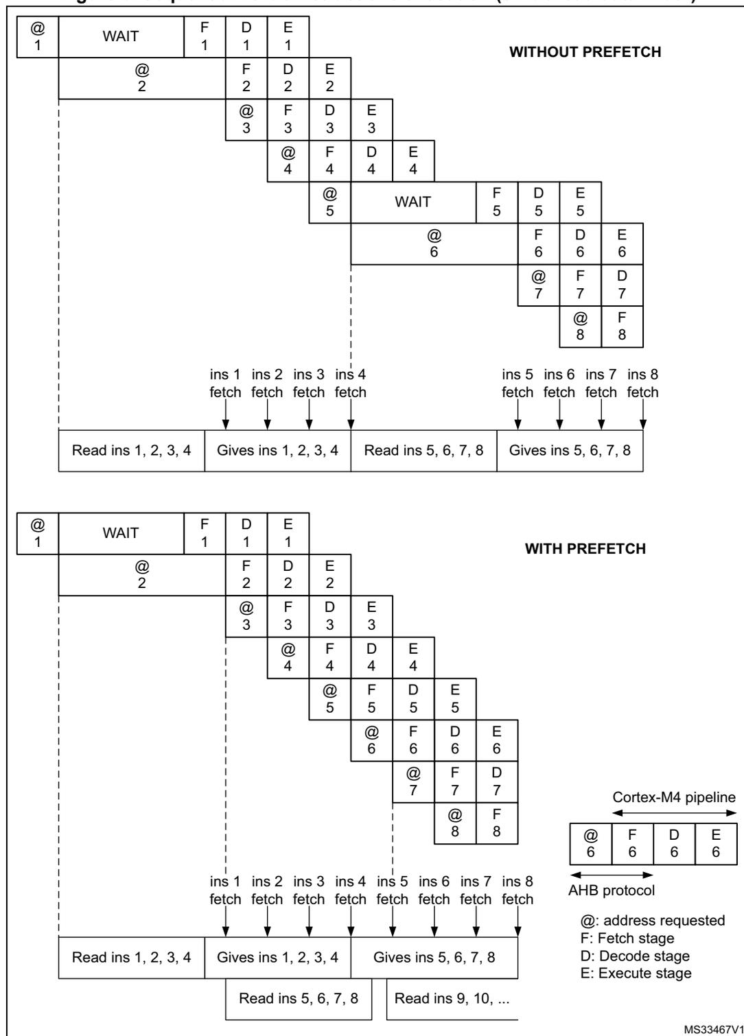
To release the processor full performance, the accelerator implements an instruction prefetch queue and branch cache which increases program execution speed from the 64-bit flash memory. Based on CoreMark benchmark, the performance achieved thanks to the ART accelerator is equivalent to 0 wait state program execution from flash memory at a CPU frequency up to 170 MHz.
Instruction prefetch
The Cortex ® -M4 fetches the instruction over the ICode bus and the literal pool (constant/data) over the DCode bus. The prefetch block aims at increasing the efficiency of ICode bus accesses.
Each flash memory read operation provides 64 bits from either two instructions of 32 bits or four instructions of 16 bits depending on the launched program. This 64-bit current instruction line is saved in a current buffer, and in case of sequential code, at least two CPU cycles are needed to execute the previous read instruction line.
Prefetch on the ICode bus can be used to read the next sequential instruction line from the flash memory while the current instruction line is being requested by the CPU.
Prefetch is enabled by setting the PRFTEN bit in the Flash access control register (FLASH_ACR) . This feature is useful if at least one wait state is needed to access the flash memory.
Figure 9 shows the execution of sequential 16-bit instructions with and without prefetch when 3 WS are needed to access the flash memory.
Figure 6. Sequential 16-bit instructions execution (64-bit read data width)
WITHOUT PREFETCH
| @ 1 | WAIT | F 1 | D 1 | E 1 | ||||||
| @ 2 | F 2 | D 2 | E 2 | |||||||
| @ 3 | F 3 | D 3 | E 3 | |||||||
| @ 4 | F 4 | D 4 | E 4 | |||||||
| @ 5 | WAIT | F 5 | D 5 | E 5 | ||||||
| @ 6 | F 6 | D 6 | E 6 | |||||||
| @ 7 | F 7 | D 7 | ||||||||
| @ 8 | F 8 |
ins 1 fetch ins 2 fetch ins 3 fetch ins 4 fetch ins 5 fetch ins 6 fetch ins 7 fetch ins 8 fetch
Read ins 1, 2, 3, 4 Gives ins 1, 2, 3, 4 Read ins 5, 6, 7, 8 Gives ins 5, 6, 7, 8
WITH PREFETCH
| @ 1 | WAIT | F 1 | D 1 | E 1 | ||||||
| @ 2 | F 2 | D 2 | E 2 | |||||||
| @ 3 | F 3 | D 3 | E 3 | |||||||
| @ 4 | F 4 | D 4 | E 4 | |||||||
| @ 5 | F 5 | D 5 | E 5 | |||||||
| @ 6 | F 6 | D 6 | E 6 | |||||||
| @ 7 | F 7 | D 7 | ||||||||
| @ 8 | F 8 |
ins 1 fetch ins 2 fetch ins 3 fetch ins 4 fetch ins 5 fetch ins 6 fetch ins 7 fetch ins 8 fetch
Read ins 1, 2, 3, 4 Gives ins 1, 2, 3, 4 Gives ins 5, 6, 7, 8
Read ins 5, 6, 7, 8 Read ins 9, 10, ...
Cortex-M4 pipeline
| @ 6 | F 6 | D 6 | E 6 |
AHB protocol
@: address requested
F: Fetch stage
D: Decode stage
E: Execute stage
MS33467V1
When the code is not sequential (branch), the instruction may not be present in the currently used instruction line or in the prefetched instruction line. In this case (miss), the penalty in terms of number of cycles is at least equal to the number of wait states.
If a loop is present in the current buffer, no new flash access is performed.
Instruction cache memory (I-Cache)
To limit the time lost due to jumps, it is possible to retain 32 lines of 4 x 64 bits in an instruction cache memory. This feature can be enabled by setting the instruction cache enable (ICEN) bit in the Flash access control register (FLASH_ACR) . Each time a miss occurs (requested data not present in the currently used instruction line, in the prefetched instruction line or in the instruction cache memory), the line read is copied into the instruction cache memory. If some data contained in the instruction cache memory are requested by the CPU, they are provided without inserting any delay. Once all the instruction cache memory lines have been filled, the LRU (least recently used) policy is used to determine the line to replace in the instruction memory cache. This feature is particularly useful in case of code containing loops.
The Instruction cache memory is enable after system reset.
Data cache memory (D-Cache)
Literal pools are fetched from flash memory through the DCode bus during the execution stage of the CPU pipeline. Each DCode bus read access fetches 64 bits which are saved in a current buffer. The CPU pipeline is consequently stalled until the requested literal pool is provided. To limit the time lost due to literal pools, accesses through the AHB databus DCode have priority over accesses through the AHB instruction bus ICode.
If some literal pools are frequently used, the data cache memory can be enabled by setting the data cache enable (DCEN) bit in the Flash access control register (FLASH_ACR) . This feature works like the instruction cache memory, but the retained data size is limited to 8 rows of 4*64 bits.
The Data cache memory is enable after system reset.
Note: The D-Cache is active only when data is requested by the CPU (not by DMA1 and DMA2). Data in option bytes block are not cacheable.
4.3.5 Flash program and erase operations
The STM32G4 series embedded flash memory can be programmed using in-circuit programming or in-application programming.
The in-circuit programming (ICP) method is used to update the entire contents of the flash memory, using the JTAG, SWD protocol or the bootloader to load the user application into the microcontroller. ICP offers quick and efficient design iterations and eliminates unnecessary package handling or socketing of devices.
In contrast to the ICP method, in-application programming (IAP) can use any communication interface supported by the microcontroller (I/Os, USB, CAN, UART, I 2 C, SPI, etc.) to download programming data into memory. IAP allows the user to reprogram the flash memory while the application is running. Nevertheless, part of the application has to have been previously programmed in the flash memory using ICP.
The contents of the flash memory are not guaranteed if a device reset occurs during a flash memory operation.
The flash erase and programming is only possible in the voltage scaling range 1. The VOS[1:0] bits in the PWR_CR1 must be programmed to 01b.
During a program/erase operation to the flash memory, any attempt to read the flash memory stalls the bus. The read operation proceeds correctly once the program/erase operation has completed.
Unlocking the flash memory
After reset, write is not allowed in the Flash control register (FLASH_CR) to protect the flash memory against possible unwanted operations due, for example, to electric disturbances. The following sequence is used to unlock this register:
- 1. Write KEY1 = 0x45670123 in the Flash key register (FLASH_KEYR)
- 2. Write KEY2 = 0xCDEF89AB in the FLASH_KEYR register.
Any wrong sequence locks up the FLASH_CR register until the next system reset. In the case of a wrong key sequence, a bus error is detected and a Hard Fault interrupt is generated.
The FLASH_CR register can be locked again by software by setting the LOCK bit in the FLASH_CR register.
Note: The FLASH_CR register cannot be written when the BSY bit in the Flash status register (FLASH_SR) is set. Any attempt to write to it with the BSY bit set causes the AHB bus to stall until the BSY bit is cleared.
4.3.6 Flash main memory erase sequences
The flash memory erase operation can be performed at page level or on the whole flash memory (mass erase). Mass erase does not affect the Information block (system flash, OTP and option bytes).
Page erase
To erase a page, follow the procedure below:
- 1. Check that no flash memory operation is ongoing by checking the BSY bit in the Flash status register (FLASH_SR) .
- 2. Check and clear all error programming flags due to a previous programming. If not, PGSERR is set.
- 3. Set the PER bit and select the page to erase (PNB).
- 4. Set the STRT bit in the FLASH_CR register.
- 5. Wait for the BSY bit to be cleared in the FLASH_SR register.
Note: The internal oscillator HSI16 (16 MHz) is enabled automatically when STRT bit is set, and disabled automatically when STRT bit is cleared, except if the HSI16 is previously enabled with HSION in RCC_CR register.
If the page erase is part of write-protected area (by WRP or PCROP), WRPERE is set and the page erase request is aborted.
Mass erase
To perform a mass erase, follow the procedure below:
- 1. Check that no flash memory operation is ongoing by checking the BSY bit in the FLASH_SR register.
- 2. Check and clear all error programming flags due to a previous programming. If not, PGSERR is set.
- 3. Set the MER1 bit in the flash memory control register (FLASH_CR).
- 4. Set the STRT bit in the FLASH_CR register.
- 5. Wait for the BSY bit to be cleared in the flash status register (FLASH_SR).
Note: The internal oscillator HSI16 (16 MHz) is enabled automatically when STRT bit is set, and disabled automatically when STRT bit is cleared, except if the HSI16 is previously enabled with HSION in RCC_CR register.
If the Flash memory contains a write-protected area (by WRP or PCROP), WRPERR is set and the mass erase request is aborted.
4.3.7 Flash main memory programming sequences
The flash memory is programmed 72 bits at a time (64 bits + 8 bits ECC).
Programming in a previously programmed address is not allowed except if the data to write is full zero, and any attempt sets PROGERR flag in the Flash status register (FLASH_SR) .
It is only possible to program double word (2 x 32-bit data).
- • Any attempt to write byte or half-word sets SIZERR flag in the FLASH_SR register.
- • Any attempt to write a double word which is not aligned with a double word address sets PGAERR flag in the FLASH_SR register.
Standard programming
The flash memory programming sequence in standard mode is as follows:
- 1. Check that no flash main memory operation is ongoing by checking the BSY bit in the Flash status register (FLASH_SR) .
- 2. Check and clear all error programming flags due to a previous programming. If not, PGSERR is set.
- 3. Set the PG bit in the Flash control register (FLASH_CR) .
- 4. Perform the data write operation at the desired memory address, inside main memory block or OTP area. Only double word can be programmed.
- – Write a first word in an address aligned with double word
- – Write the second word
- 5. Wait until the BSY bit is cleared in the FLASH_SR register.
- 6. Check that EOP flag is set in the FLASH_SR register (meaning that the programming operation has succeed), and clear it by software.
- 7. Clear the PG bit in the FLASH_SR register if there no more programming request anymore.
Note: When the flash interface has received a good sequence (a double word), programming is automatically launched and BSY bit is set. The internal oscillator HSI16 (16 MHz) is enabled
automatically when PG bit is set, and disabled automatically when PG bit is cleared, except if the HSI16 is previously enabled with HSION in RCC_CR register.
If the user needs to program only one word, double word must be completed with the erase value 0xFFFF FFFF to launch automatically the programming.
ECC is calculated from the double word to program.
Fast programming
This mode allows to program a row (32 double words), and to reduce the page programming time by eliminating the need for verifying the flash locations before they are programmed and to avoid rising and falling time of high voltage for each double word. During fast programming, the CPU clock frequency (HCLK) must be at least 8 MHz.
Only the main memory can be programmed in Fast programming mode.
The flash main memory programming sequence in standard mode is as follows:
- 1. Perform a mass erase. If not, PGSERR is set.
- 2. Check that no flash main memory operation is ongoing by checking the BSY bit in the Flash status register (FLASH_SR) .
- 3. Check and clear all error programming flag due to a previous programming.
- 4. Set the FSTPG bit in Flash control register (FLASH_CR) .
- 5. Write the 32 double words to program a row. Only double words can be programmed:
- – Write a first word in an address aligned with double word
- – Write the second word.
- 6. Wait until the BSY bit is cleared in the FLASH_SR register.
- 7. Check that EOP flag is set in the FLASH_SR register (meaning that the programming operation has succeed), and clear it by software.
- 8. Clear the FSTPG bit in the FLASH_SR register if there no more programming request anymore.
Note: If the flash is attempted to be written in Fast programming mode while a read operation is on going, the programming is aborted without any system notification (no error flag is set).
When the flash interface has received the first double word, programming is automatically launched. The BSY bit is set when the high voltage is applied for the first double word, and it is cleared when the last double word has been programmed or in case of error. The internal oscillator HSI16 (16 MHz) is enabled automatically when FSTPG bit is set, and disabled automatically when FSTPG bit is cleared, except if the HSI16 is previously enabled with HSION in RCC_CR register.
The 32 double word must be written successively. The high voltage is kept on the flash for all the programming. Maximum time between two double words write requests is the time programming (around 2 x 25 µs). If a second double word arrives after this time programming, fast programming is interrupted and MISSERR is set.
High voltage cannot exceed 8 ms for a full row between two erases. This is guaranteed by the sequence of 32 double words successively written with a clock system greater or equal to 8 MHz. An internal time-out counter counts 7ms when Fast programming is set and stops the programming when time-out is over. In this case the FASTERR bit is set.
If an error occurs, high voltage is stopped and next double word to programmed is not programmed. Anyway, all previous double words have been properly programmed.
Programming errors
Several kind of errors can be detected. In case of error, the flash memory operation (programming or erasing) is aborted.
- • PROGERR: Programming error
In standard programming: PROGERR is set if the word to write is not previously erased (except if the value to program is full zero).
- • SIZERR: Size programming error
In standard programming or in fast programming: only double word can be programmed and only 32-bit data can be written. SIZERR is set if a byte or an half-word is written.
- • PGAERR: Alignment programming error
PGAERR is set if one of the following conditions occurs:
- – In standard programming: the first word to be programmed is not aligned with a double word address, or the second word doesn't belong to the same double word address.
- – In fast programming: the data to program doesn't belong to the same row than the previous programmed double words, or the address to program is not greater than the previous one.
- • PGSERR: Programming sequence error
PGSERR is set if one of the following conditions occurs:
- – In the standard programming sequence or the fast programming sequence: a data is written when PG and FSTPG are cleared.
- – In the standard programming sequence or the fast programming sequence: MER1, and PER are not cleared when PG or FSTPG is set.
- – In the fast programming sequence: the mass erase is not performed before setting FSTPG bit.
- – In the mass erase sequence: PG, FSTPG, and PER are not cleared when MER1 is set.
- – In the page erase sequence: PG, FSTPG, MER1 are not cleared when PER is set.
- – PGSERR is set also if PROGERR, SIZERR, PGAERR, WRPERR, MISSERR, FASTERR or PGSERR is set due to a previous programming error.
- • WRPERR: Write protection error
WRPERR is set if one of the following conditions occurs:
- – Attempt to program or erase in a write protected area (WRP) or in a PCROP area or in a securable memory area.
- – Attempt to perform an erase when one page or more is protected by WRP or PCROP.
- – The debug features are connected or the boot is executed from SRAM or from System flash when the read protection (RDP) is set to Level 1.
- – Attempt to modify the option bytes when the read protection (RDP) is set to Level 2.
- • MISSERR: Fast programming data miss error
In fast programming: all the data must be written successively. MISSERR is set if the previous data programming is finished and the next data to program is not written yet.
- • FASTERR: Fast programming error
In fast programming: FASTERR is set if one of the following conditions occurs:
- – When FSTPG bit is set for more than 7ms which generates a time-out detection.
- – When the fast programming has been interrupted by a MISSERR, PGAERR, WRPERR or SIZERR.
If an error occurs during a program or erase operation, one of the following error flags is set in the FLASH_SR register:
PROGERR, SIZERR, PGAERR, PGSERR, MISSERR (Program error flags),
WRPERR (Protection error flag)
In this case, if the error interrupt enable bit ERRIE is set in the Flash status register (FLASH_SR) , an interrupt is generated and the operation error flag OPERR is set in the FLASH_SR register.
Note: If several successive errors are detected (for example, in case of DMA transfer to the flash memory), the error flags cannot be cleared until the end of the successive write requests.
Programming and caches
If a flash memory write access concerns some data in the data cache, the flash write access modifies the data in the flash memory and the data in the cache.
If an erase operation in flash memory also concerns data in the data or instruction cache, you have to make sure that these data are rewritten before they are accessed during code execution. If this cannot be done safely, it is recommended to flush the caches by setting the DCRST and ICRST bits in the Flash access control register (FLASH_ACR) .
Note: The I/D cache should be flushed only when it is disabled (I/DCEN = 0).
4.4 FLASH option bytes
4.4.1 Option bytes description
The option bytes are configured by the end user depending on the application requirements. As a configuration example, the watchdog can be selected in hardware or software mode (refer to Section 5.4.2: Option bytes programming ).
A double word is split up as follows in the option bytes:
Table 20. Option byte format
| 63-24 | 23-16 | 15 -8 | 7-0 | 31-24 | 23-16 | 15 -8 | 7-0 |
|---|---|---|---|---|---|---|---|
| Complemented option byte 3 | Complemented option byte 2 | Complemented option byte 1 | Complemented option byte 0 | Option byte 3 | Option byte 2 | Option byte 1 | Option byte 0 |
The organization of these bytes inside the information block is as shown in Table 31: Option byte organization .
The option bytes can be read from the memory locations listed in Table 31: Option byte organization or from the Option byte registers:
- • Flash option register (FLASH_OPTR)
- • Flash PCROP1 Start address register (FLASH_PCROP1SR)
- • Flash PCROP1 End address register (FLASH_PCROP1ER)
- • Flash WRP area A address register (FLASH_WRP1AR)
- • Flash WRP area B address register (FLASH_WRP1BR)
Table 21. Option byte organization (1)
| Address | [63:56] | [55:48] | [47:40] | [39:32] | [31:24] | [23:16] | [15:8] | [7:0] |
|---|---|---|---|---|---|---|---|---|
| 1FFF7800 | USER OPT | RDP | USER OPT | RDP | ||||
| 1FFF7808 | Unused | Unused and PCROP1_STRT[15:0] | Unused | Unused and PCROP1_STRT[15:0] | ||||
| 1FFF7810 | PCROP_RDP and Unused | Unused and PCROP1_END[15:0] | PCROP_RDP and Unused | Unused and PCROP1_END[15:0] | ||||
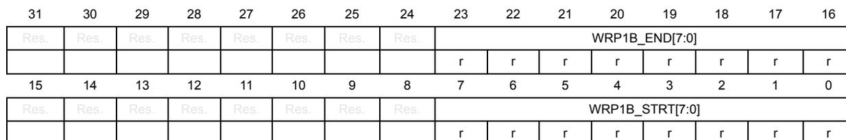
| 1FFF7818 | Unused | WRP1A_END [7:0] | Unused | WRP1A_STRT [7:0] | Unused | WRP1A_END [7:0] | Unused | WRP1A_STRT [7:0] |
| 1FFF7820 | Unused | WRP1B_END [7:0] | Unused | WRP1B_STRT [7:0] | Unused | WRP1B_END [7:0] | Unused | WRP1B_STRT [7:0] |
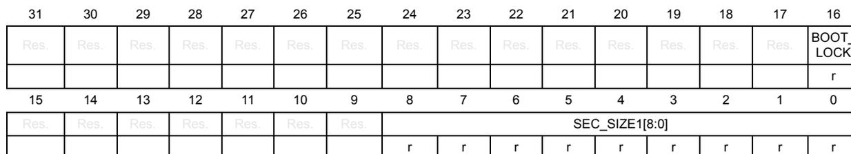
| 1FFF7828 | Unused | BOOT_LOCK | Unused | SEC_SIZE1 | Unused | BOOT_LOCK | Unused | SEC_SIZE1 |
1. Negated values are overlined.
User and read protection option bytes
Flash memory address: 0x1FFF 7800
ST production value: 0xFFEF F8AA
| 31 | 30 | 29 | 28 | 27 | 26 | 25 | 24 | 23 | 22 | 21 | 20 | 19 | 18 | 17 | 16 |
|---|---|---|---|---|---|---|---|---|---|---|---|---|---|---|---|
| Res. | IRH_EN | NRST_MODE [1:0] | nBOOT0 | nSWBOOT0 | CCMSRAM_RST | SRAM_PE | nBOOT1 | PB4_PUPEN | Res. | Res. | WWDG_SW | IWDG_STDBY | IWDG_STOP | IWDG_SW | |
| r | r r | r | r | r | r | r | r | r | r | r | r | ||||
| 15 | 14 | 13 | 12 | 11 | 10 | 9 | 8 | 7 | 6 | 5 | 4 | 3 | 2 | 1 | 0 |
|---|---|---|---|---|---|---|---|---|---|---|---|---|---|---|---|
| Res. | nRST_SHDW | nRST_STDBY | nRST_STOP | Res. | BOR_LEV[2:0] | RDP[7:0] | |||||||||
| r | r | r | r | r | r | r | r | r | r | r | r | r | r | ||
Bit 31 Reserved, keep to 1 during option bytes programming.
Bit 30 IRH_EN : Internal reset holder on NRST pin
0: IRH disabled
1: IRH enabled
Bits 29:28 NRST_MODE[1:0] : PG10 pad mode
00: Reset Input/Output
01: Reset Input only
10: GPIO
11: Reset Input/Output
Bit 27 nBOOT0 : nBOOT0 option bit
0: nBOOT0 = 0
1: nBOOT0 = 1
Bit 26 nSWBOOT0 : Software BOOT0
0: BOOT0 taken from the option bit nBOOT0
1: BOOT0 taken from PB8/BOOT0 pin
Bit 25 CCMSRAM_RST : CCM SRAM erase when system reset
0: CCM SRAM erased when a system reset occurs
1: CCM SRAM is not erased when a system reset occurs
Bit 24 SRAM_PE : SRAM1 and CCM SRAM parity check enable
0: SRAM1 and CCM SRAM parity check enable
1: SRAM1 and CCM SRAM parity check disable
Bit 23 nBOOT1 : Boot configuration
Together with the BOOT0 pin, this bit selects boot mode from the flash main memory, SRAM1 or the System memory. Refer to Section 2.6: Boot configuration .
Bit 22 PB4_PUPEN : PB4 pull-up enable
0: USB power delivery dead-battery enabled/NJTRST pull-up deactivated
1: USB power delivery dead-battery disabled/NJTRST pull-up activated
Note: Only for Category 4 devices (otherwise Reserved)
Bits 21:20 Reserved, keep to 1 during option bytes programming.
Bit 19 WWDG_SW : Window watchdog selection
0: Hardware window watchdog
1: Software window watchdog
Bit 18 IWDG_STDBY : Independent watchdog counter freeze in Standby mode
0: Independent watchdog counter is frozen in Standby mode
1: Independent watchdog counter is running in Standby mode
Bit 17 IWDG_STOP : Independent watchdog counter freeze in Stop mode
0: Independent watchdog counter is frozen in Stop mode
1: Independent watchdog counter is running in Stop mode
Bit 16 IWDG_SW : Independent watchdog selection
0: Hardware independent watchdog
1: Software independent watchdog
Bit 15 Reserved, keep to 1 during option bytes programming.
Bit 14 nRST_SHDW
0: Reset generated when entering the Shutdown mode
1: No reset generated when entering the Shutdown mode
Bit 13 nRST_STDBY
0: Reset generated when entering the Standby mode
1: No reset generate when entering the Standby mode
Bit 12 nRST_STOP
0: Reset generated when entering the Stop mode
1: No reset generated when entering the Stop mode
Bit 11 Reserved, keep to 1 during option bytes programming.
Bits 10:8 BOR_LEV : BOR reset level
These bits contain the VDD supply level threshold that activates/releases the reset.
000: BOR level 0. Reset level threshold is around 1.7 V
001: BOR level 1. Reset level threshold is around 2.0 V
010: BOR level 2. Reset level threshold is around 2.2 V
011: BOR level 3. Reset level threshold is around 2.5 V
100: BOR level 4. Reset level threshold is around 2.8 V
Bits 7:0 RDP : Read protection level
0xAA: Level 0, read protection not active
0xCC: Level 2, chip read protection active
Others: Level 1, memories read protection active
PCROP1 Start address option bytes
Flash memory address: 0x1FFF 7808
Reset value: 0xFFFF FFFF (ST production value)
| 31 | 30 | 29 | 28 | 27 | 26 | 25 | 24 | 23 | 22 | 21 | 20 | 19 | 18 | 17 | 16 |
|---|---|---|---|---|---|---|---|---|---|---|---|---|---|---|---|
| Res | Res | Res | Res | Res | Res | Res | Res | Res | Res | Res | Res | Res | Res | Res | Res |
| 15 | 14 | 13 | 12 | 11 | 10 | 9 | 8 | 7 | 6 | 5 | 4 | 3 | 2 | 1 | 0 |
| PCROP1_STR[15:0] | |||||||||||||||
| r | r | r | r | r | r | r | r | r | r | r | r | r | r | r | r |
Bits 31:16 Reserved, keep to 1 during option bytes programming.
Bits 15:0 PCROP1_STRT[15:0] : PCROP area start offset
PCROP1_STRT contains the first double-word of the PCROP area for bank1.
PCROP1 End address option bytes
Flash memory address: 0x1FFF 7810
Reset value: 0x00FF 0000 (ST production value)
Note: All reserved bits are set after first reprogramming (with no possibility to reset them back).
| 31 | 30 | 29 | 28 | 27 | 26 | 25 | 24 | 23 | 22 | 21 | 20 | 19 | 18 | 17 | 16 |
|---|---|---|---|---|---|---|---|---|---|---|---|---|---|---|---|
| PCROP_RDP | Res. | Res. | Res. | Res. | Res. | Res. | Res. | Res. | Res. | Res. | Res. | Res. | Res. | Res. | Res. |
| r | |||||||||||||||
| 15 | 14 | 13 | 12 | 11 | 10 | 9 | 8 | 7 | 6 | 5 | 4 | 3 | 2 | 1 | 0 |
| PCROP1_END[15:0] | |||||||||||||||
| r | r | r | r | r | r | r | r | r | r | r | r | r | r | r | r |
Bit 31 PCROP_RDP : PCROP area preserved when RDP level decreased
This bit is set only. It is reset after a full mass erase due to a change of RDP from Level 1 to Level 0.
0: PCROP area is not erased when the RDP level is decreased from Level 1 to Level 0.
1: PCROP area is erased when the RDP level is decreased from Level 1 to Level 0 (full mass erase).
Bits 30:16 Reserved, keep to 1 during option bytes programming.
Bits 15:0 PCROP1_END[15:0] : Bank 1 PCROP area end offset
PCROP1_END contains the last double-word of the PCROP area.
WRP1 Area A address option bytes
Flash memory address: 0x1FFF 7818
Reset value: 0xFF00 FFFF (ST production value)
Note: All reserved bits are set after first reprogramming (with no possibility to reset them back).
| 31 | 30 | 29 | 28 | 27 | 26 | 25 | 24 | 23 | 22 | 21 | 20 | 19 | 18 | 17 | 16 |
|---|---|---|---|---|---|---|---|---|---|---|---|---|---|---|---|
| Res. | Res. | Res. | Res. | Res. | Res. | Res. | Res. | ||||||||
| r | r | r | r | r | r | r | r | ||||||||
| 15 | 14 | 13 | 12 | 11 | 10 | 9 | 8 | 7 | 6 | 5 | 4 | 3 | 2 | 1 | 0 |
| Res. | Res. | Res. | Res. | Res. | Res. | Res. | Res. | WRP1A_STR[7:0] | |||||||
| r | r | r | r | r | r | r | r | ||||||||
Bits 31:24 Reserved, keep to 1 during option bytes programming.
Bits 23:16 WRP1A_END[7:0] : WRP first area "A" end offset
WRP1A_END contains the last page of WRP first area.
Bits 15:8 Reserved, keep to 1 during option bytes programming.
Bits 7:0 WRP1A_STR[7:0] : WRP first area "A" start offset
WRP1A_STR contains the first page of WRP first area.
WRP1 Area B address option bytes
Flash memory address: 0x1FFF 7820
Reset value: 0xFF00 FFFF (ST production value)
| 31 | 30 | 29 | 28 | 27 | 26 | 25 | 24 | 23 | 22 | 21 | 20 | 19 | 18 | 17 | 16 |
| Res. | Res. | Res. | Res. | Res. | Res. | Res. | Res. | WRP1B_END[7:0] | |||||||
| r | r | r | r | r | r | r | r | ||||||||
| 15 | 14 | 13 | 12 | 11 | 10 | 9 | 8 | 7 | 6 | 5 | 4 | 3 | 2 | 1 | 0 |
| Res. | Res. | Res. | Res. | Res. | Res. | Res. | Res. | WRP1B_STRT[7:0] | |||||||
| r | r | r | r | r | r | r | r | ||||||||
Bits 31:24 Reserved, keep to 1 during option bytes programming.
Bits 23:16 WRP1B_END[7:0] : WRP second area “B” end offset
WRP1B_END contains the last page of the WRP second area.
Bits 15:8 Reserved, keep to 1 during option bytes programming.
Bits 7:0 WRP1B_STRT[7:0] : WRP second area start offset
WRP1B_STRT contains the first page of the WRP second area.
Securable memory area option bytes
Flash memory address: 0x1FFF7828
Reset value: 0xFF00FE00 (ST production value)
Note: All reserved bits are set after first reprogramming (with no possibility to reset them back).
| 31 | 30 | 29 | 28 | 27 | 26 | 25 | 24 | 23 | 22 | 21 | 20 | 19 | 18 | 17 | 16 |
| Res. | Res. | Res. | Res. | Res. | Res. | Res. | Res. | Res. | Res. | Res. | Res. | Res. | Res. | Res. | BOOT_LOCK |
| r | |||||||||||||||
| 15 | 14 | 13 | 12 | 11 | 10 | 9 | 8 | 7 | 6 | 5 | 4 | 3 | 2 | 1 | 0 |
| Res. | Res. | Res. | Res. | Res. | Res. | Res. | SEC_SIZE1[8:0] | ||||||||
| r | r | r | r | r | r | r | r | r | |||||||
Bits 31:17 Reserved, keep to 1 during option bytes programming.
Bit 16 BOOT_LOCK : used to force boot from user area
0: Boot based on the pad/option bit configuration
1: Boot forced from main flash memory
Bits 15:9 Reserved, keep to 1 during option bytes programming.
Bits 8:0 SEC_SIZE1[8:0] : Securable memory area size
Contains the number of securable flash memory pages
4.4.2 Option bytes programming
After reset, the options related bits in the Flash control register (FLASH_CR) are write-protected. To run any operation on the option bytes page, the option lock bit OPTLOCK in the Flash control register (FLASH_CR) must be cleared. The following sequence is used to unlock this register:
- 1. Unlock the FLASH_CR with the LOCK clearing sequence (refer to Unlocking the flash memory ).
- 2. Write OPTKEY1 = 0x08192A3B in the Flash option key register (FLASH_OPTKEYR) .
- 3. Write OPTKEY2 = 0x4C5D6E7F in the FLASH_OPTKEYR register.
The user options can be protected against unwanted erase/program operations by setting the OPTLOCK bit by software.
Note: If LOCK is set by software, OPTLOCK is automatically set too.
Modifying user options
The option bytes are programmed differently from a main memory user address. To modify the user options value, follow the procedure below:
- 1. Check that no flash memory operation is on going by checking the BSY bit in the Flash status register (FLASH_SR) .
- 2. Clear OPTLOCK option lock bit with the clearing sequence described above.
- 3. Write the desired options value in the options registers: Flash option register (FLASH_OPTR) , Flash PCROP1 Start address register (FLASH_PCROP1SR) , Flash PCROP1 End address register (FLASH_PCROP1ER) , Flash WRP area A address register (FLASH_WRP1AR) , Flash WRP area B address register (FLASH_WRP1BR) , Flash securable area register (FLASH_SEC1R) .
- 4. Set the bit OPTSTRT in the Flash control register (FLASH_CR) .
- 5. Wait for the BSY bit to be cleared.
Note: Any modification of the value of one option is automatically performed by erasing both user option bytes pages first and then programming all the option bytes with the values contained in the flash option registers.
Option byte loading
After the BSY bit is cleared, all new options are updated into the flash but they are not applied to the system. They have effect on the system when they are loaded. Option bytes loading (OBL) is performed in two cases:
- – when OBL_LAUNCH bit is set in the Flash control register (FLASH_CR) .
- – after a power reset (BOR reset or exit from Standby/Shutdown modes).
Option byte loader performs a read of the options block and stores the data into internal option registers. These internal registers configure the system and cannot be read with by software. Setting OBL_LAUNCH generates a reset so the option byte loading is performed under system reset.
Each option bit has also its complement in the same double word. During option loading, a verification of the option bit and its complement allows to check the loading has correctly taken place.
During option byte loading, the options are read by double word with ECC. If the word and its complement are matching, the option word/byte is copied into the option register.
If the comparison between the word and its complement fails, a status bit OPTVERR is set. Mismatch values are forced into the option registers:
- – For USR OPT option, the value of mismatch is all options at '1', except for BOR_LEV which is "000" (lowest threshold)
- – For WRP option, the value of mismatch is the default value "No protection"
- – For RDP option, the value of mismatch is the default value "Level 1"
- – For PCROP, the value of mismatch is "all memory protected"
On system reset rising, internal option registers are copied into option registers which can be read and written by software (FLASH_OPTR, FLASH_PCROP1SR, FLASH_PCROP1ER, FLASH_WRP1AR, FLASH_WRP1BR). These registers are also used to modify options. If these registers are not modified by user, they reflect the options states of the system. See Modifying user options for more details.
4.5 FLASH memory protection
The flash main memory can be protected against external accesses with the Read protection (RDP). The pages of the flash memory can also be protected against unwanted write due to loss of program counter contexts. The write-protection (WRP) granularity is one page (2 Kbytes). Apart of the flash memory can also be protected against read and write from third parties (PCROP). The PCROP granularity is double word (64-bit).
4.5.1 Read protection (RDP)
The read protection is activated by setting the RDP option byte and then, by applying a system reset to reload the new RDP option byte. The read protection protects to the flash main memory, the option bytes, the backup registers (TAMP_BKPxR in the RTC) and the CCM SRAM.
Note: If the read protection is set while the debugger is still connected (or had been connected since the last power on) through JTAG/SWD, apply a POR (power-on reset) instead of a system reset. If the read protection is programmed through software, don't set the OBL_LAUNCH bit (FLASH_CR register) but perform a POR to reload the option byte. This can be done with a transition Standby (or Shutdown) mode followed by a wakeup.
There are three levels of read protection from no protection (level 0) to maximum protection or no debug (level 2).
The flash memory is protected when the RDP option byte and its complement contain the pair of values shown in Table 32 .
Table 22. Flash memory read protection status
| RDP byte value | RDP complement value | Read protection level |
|---|---|---|
| 0xAA | 0x55 | Level 0 (production value) |
| Any value except 0xAA or 0xCC | Any value (not necessarily complementary) except 0x55 and 0x33 | Level 1 |
| 0xCC | 0x33 | Level 2 |
The System memory area is read accessible whatever the protection level. It is never accessible for program/erase operation.
Level 0: no protection
Read, program and erase operations into the flash main memory area are possible. The option bytes, the CCM SRAM and the backup registers are also accessible by all operations.
Level 1: Read protection
This is the default protection level when RDP option byte is erased. It is defined as well when RDP value is at any value different from 0xAA and 0xCC, or even if the complement is not correct.
- • User mode: Code executing in user mode ( Boot Flash ) can access flash main memory, option bytes, CCM SRAM and backup registers with all operations.
- • Debug, boot RAM and bootloader modes: In debug mode or when code is running from boot RAM or bootloader, the flash main memory, the backup registers (TAMP_BKPxR in the RTC) and the CCM SRAM are totally inaccessible. In these modes, a read or write access to the flash generates a bus error and a Hard Fault interrupt.
Caution: In case the Level 1 is configured and no PCROP area is defined, it is mandatory to set PCROP_RDP bit to 1 (full mass erase when the RDP level is decreased from Level 1 to Level 0). In case the Level 1 is configured and a PCROP area is defined, if user code needs to be protected by RDP but not by PCROP, it must not be placed in a page containing a PCROP area.
Level 2: No debug
In this level, the protection level 1 is guaranteed. In addition, the Cortex®-M4 debug port (boundary scan TAP and Cortex®-M4 with FPU TAP), the boot from RAM (boot RAM mode) and the boot from System memory (bootloader mode) are no more available. In user execution mode (boot FLASH mode), all operations are allowed on the flash main memory. On the contrary, only read operations can be performed on the option bytes.
Option bytes cannot be programmed nor erased. Thus, the level 2 cannot be removed at all: it is an irreversible operation. When attempting to modify the options bytes, the protection error flag WRPERR is set in the Flash_SR register and an interrupt can be generated.
Note: The debug feature is also disabled under reset.
STMicroelectronics is not able to perform analysis on defective parts on which the level 2 protection has been set.
Changing the Read protection level
It is easy to move from level 0 to level 1 by changing the value of the RDP byte to any value (except 0xCC). By programming the 0xCC value in the RDP byte, it is possible to go to level 2 either directly from level 0 or from level 1. Once in level 2, it is no more possible to modify the Read protection level.
When the RDP is reprogrammed to the value 0xAA to move from Level 1 to Level 0, a mass erase of the flash main memory is performed if PCROP_RDP is set in the Flash PCROP1 End address register (FLASH_PCROP1ER) . The backup registers (TAMP_BKPxR in the RTC) and the CCM SRAM are also erased. The user options except PCROP protection are set to their previous values copied from FLASH_OPTR, FLASH_WRPxyR (x=1 and y =A or B). PCROP is disable. The OTP area is not affected by mass erase and remains unchanged.
If the bit PCROP_RDP is cleared in the FLASH_PCROP1ER, the full mass erase is replaced by a partial mass erase that is successive page erases, except for the pages protected by PCROP. This is done in order to keep the PCROP code. Only when the flash memory is erased, options are re-programmed with their previous values. This is also true for FLASH_PCROPxSR and FLASH_PCROPxER registers (x=1).
Note: Full mass erase or partial mass erase is performed only when Level 1 is active and Level 0 requested. When the protection level is increased (0->1, 1->2, 0->2) there is no mass erase. To validate the protection level change, the option bytes must be reloaded through the OBL_LAUNCH bit in flash control register.
Figure 7. Changing the read protection (RDP) level
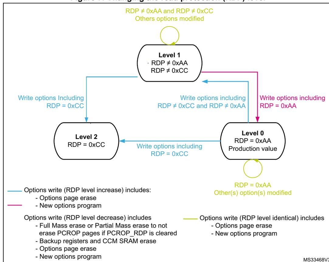
Legend:
- —
Options write (RDP level increase) includes:
- - Options page erase
- - New options program
- —
Options write (RDP level identical) includes:
- - Options page erase
- - New options program
- Options write (RDP level decrease) includes:
- - Full Mass erase or Partial Mass erase to not erase PCROP pages if PCROP_RDP is cleared
- - Backup registers and CCM SRAM erase
- - Options page erase
- - New options program
MS33468V3
Table 23. Access status versus protection level and execution modes
| Area | Protection level | User execution (BootFromFlash) | Debug/ BootFromRam/ BootFromLoader (1) | ||||
|---|---|---|---|---|---|---|---|
| Read | Write | Erase | Read | Write | Erase | ||
| Flash main memory | 1 | Yes | Yes | Yes | No | No | No (3) |
| 2 | Yes | Yes | Yes | N/A | N/A | N/A | |
| System memory (2) | 1 | Yes | No | No | Yes | No | No |
| 2 | Yes | No | No | N/A | N/A | N/A | |
Table 23. Access status versus protection level and execution modes (continued)
| Area | Protection level | User execution (BootFromFlash) | Debug/ BootFromRam/ BootFromLoader (1) | ||||
|---|---|---|---|---|---|---|---|
| Read | Write | Erase | Read | Write | Erase | ||
| Option bytes | 1 | Yes | Yes (3) | Yes | Yes | Yes (3) | Yes |
| 2 | Yes | No | No | N/A | N/A | N/A | |
| OTP | 1 | Yes | Yes (4) | N/A | No | No | N/A |
| 2 | Yes | Yes (4) | N/A | N/A | N/A | N/A | |
| Backup registers | 1 | Yes | Yes | N/A | No | No | No (5) |
| 2 | Yes | Yes | N/A | N/A | N/A | N/A | |
| CCM SRAM | 1 | Yes | Yes | N/A | No | No | No (6) |
| 2 | Yes | Yes | N/A | N/A | N/A | N/A | |
- 1. When the protection level 2 is active, the Debug port, the boot from RAM and the boot from system memory are disabled.
- 2. The system memory is only read-accessible, whatever the protection level (0, 1 or 2) and execution mode.
- 3. The flash main memory is erased when the RDP option byte is programmed with all level protections disabled (0xAA).
- 4. OTP can only be written once.
- 5. The backup registers are erased when RDP changes from level 1 to level 0.
- 6. The CCM SRAM is erased when RDP changes from level 1 to level 0.
4.5.2 Proprietary code readout protection (PCROP)
Apart of the flash memory can be protected against read and write from third parties. The protected area is execute-only: it can only be reached by the STM32 CPU, as an instruction code, while all other accesses (DMA, debug and CPU data read, write and erase) are strictly prohibited. The PCROP area has a double word (64-bit) granularity. An additional option bit (PCROP_RDP) allows to select if the PCROP area is erased or not when the RDP protection is changed from Level 1 to Level 0 (refer to Changing the Read protection level ).
Each PCROP area is defined by a start page offset and an end page offset related to the physical flash memory address. These offsets are defined in the PCROP address registers Flash PCROP1 Start address register (FLASH_PCROP1SR) , Flash PCROP1 End address register (FLASH_PCROP1ER) .
- • The PCROP x (x = 1) area is defined from the address: flash memory base address + [PCROP x _STRT x 0x8] (included) to the address: flash memory base address + [(PCROP x _END+1) x 0x8] (excluded). The minimum PCROP area size is two double-words (128 bits).
For example, to protect by PCROP from the address 0x0806 2F80 (included) to the address 0x0807 0004 (included):
- • if boot in flash is selected, FLASH_PCROP1SR and FLASH_PCROP1ER registers must be programmed with:
- – PCROP1_STRT = 0xC5F0.
- – PCROP1_END = 0xE000.
Any read access performed through the D-bus to a PCROP protected area triggers RDERR flag error.
Any PCROP protected address is also write protected and any write access to one of these addresses triggers WRPERR.
Any PCROP area is also erase protected. Consequently, any erase to a page in this zone is impossible (including the page containing the start address and the end address of this zone). A software mass erase cannot be performed if one zone is PCROP protected.
For previous example, due to erase by page, all pages from page 0xC5 to 0xE0 are protected in case of page erase. (All addresses from 0x0806 2800 to 0x0807 07FF can't be erased).
Deactivation of PCROP can only occur when the RDP is changing from level 1 to level 0. If the user options modification tries to clear PCROP or to decrease the PCROP area, the options programming is launched but PCROP area stays unchanged. On the contrary, it is possible to increase the PCROP area.
When option bit PCROP_RDP is cleared, when the RDP is changing from level 1 to level 0, mass erase is replaced by partial mass erase to keep the PCROP area (refer to Changing the Read protection level ). In this case, PCROP1_STRT and PCROP1_END are also not erased.
Note: It is recommended to align PCROP area with page granularity when using PCROP_RDP, or to leave free the rest of the page where PCROP zone starts or ends.
Table 24. PCROP protection (1)
| PCROPx registers values (x = 1) | PCROP protection area |
|---|---|
| PCROPx_offset_strt > PCROPx_offset_end | No PCROP area. |
| PCROPx_offset_strt < PCROPx_offset_end | The area between PCROPx_offset_strt and PCROPx_offset_end is protected. it is possible to write: – PCROPx_offset_strt with a lower value – PCROPx_offset_end with a higher value. |
1. The minimum PCROP area size is 2xdouble words: PCROPx_offset_strt and PCROPx_offset_end.
4.5.3 Write protection (WRP)
The user area in flash memory can be protected against unwanted write operations. It allows either to specify:
- Two write-protected (WRP) areas can be defined, with page (2 Kbytes) granularity.
Each area is defined by a start page offset and an end page offset related to the physical flash base address. These offsets are defined in the WRP address registers: Flash WRP area A address register (FLASH_WRP1AR) , Flash WRP area B address register (FLASH_WRP1BR) .
The WRP “y” area (x=1 and y=A,B) is defined from the address: Flash memory Base address + [WRPx_y_STRt x 0x800] (included) to the address: Flash memory Base address + [(WRPx_y_END+1) x 0x800] (excluded) .
For example, to protect by WRP from the address 0x0801 2800 (included) to the address 0x0801 87FF (included):
- • if boot in flash is selected, FLASH_WRP1AR register must be programmed with:
- – WRP1A_STRT = 0x25.
- – WRP1A_END = 0x30.
WRP1B_STRT and WRP1B_END in FLASH_WRP1BR can be used instead (area “B” in the flash memory).
When WRP is active, it cannot be erased or programmed. Consequently, a software mass erase cannot be performed if one area is write-protected.
If an erase/program operation to a write-protected part of the flash memory is attempted, the write protection error flag (WRPERR) is set in the FLASH_SR register. This flag is also set for any write access to:
- – OTP area
- – part of the flash memory that can never be written like the ICP
- – PCROP area.
Note: When the memory read protection level is selected (RDP level = 1), it is not possible to program or erase flash memory if the CPU debug features are connected (JTAG or single wire) or boot code is being executed from RAM or System flash, even if WRP is not activated.
Note: To validate the WRP options, the option bytes must be reloaded through the OBL_LAUNCH bit in flash control register.
Table 25. WRP protection
| WRP registers values (x=1 y= A/B) | WRP protection area |
|---|---|
| WRPxy_STRT = WRPxy_END | Page WRPxy is protected. |
| WRPxy_STRT > WRPxy_END | No WRP area. |
| WRPxy_STRT < WRPxy_END | The pages from WRPxy_STRT to WRPxy_END are protected. |
4.5.4 Securable memory area
This is an area of code that can be executed only once at boot, and never again unless a new reset occurs. The main purpose of the securable memory area is to protect a specific part of flash memory against undesired access. This allows implementing software security services such as secure key storage or safe boot. Securable memory area is located in the main flash memory. It is dedicated to executing trusted code. When not secured, the securable memory behaves like the remainder of main flash memory. When secured (the SEC_PROT1 bit of the FLASH_CR register set), any attempt to program or erase in a secure memory area generates a write protection error (WRPERR flag is set) and any attempt to read from it generates a read error (RDERR flag is set).
The size of the securable memory area is defined by the SEC_SIZE1[8:0] bitfield of the FLASH_SEC register. It can be modified only in RDP Level 0. Its content is erased upon changing from RDP Level 1 to Level 0, even if it overlaps with PCROP pages.
The securable memory area is defined from the address: Bank base address (included) to the address: Bank base address + (0x800 * SEC_SIZE1) (excluded).
4.5.5 Disabling core debug access
For executing sensitive code or manipulating sensitive data in securable memory area, the debug access to the core can temporarily be disabled.
In RDP level 2, the debugger is disabled by hardware, , but in other RDP levels, the debugger can be disabled by software using the bit DBG_SWEN in the FLASH_ACR register.
Figure 11 gives an example of managing DBG_SWEN and SEC_PROT bits.
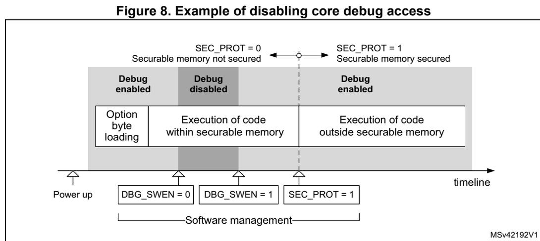
Figure 8. Example of disabling core debug access
The diagram illustrates the sequence of events to disable core debug access. It starts with 'Power up', followed by 'SEC_PROT = 0' (Securable memory not secured) and 'DBG_SWEN = 0' (Debug enabled). Then 'DBG_SWEN = 1' is set (Debug disabled). Finally, 'SEC_PROT = 1' is set (Securable memory secured) and 'DBG_SWEN = 0' is reset (Debug enabled). The diagram also shows 'Option byte loading', 'Execution of code within securable memory', and 'Execution of code outside securable memory'.
MSV42192V1
4.5.6 Forcing boot from flash memory
To increase the security and establish a chain of trust, thanks to BOOT_LOCK option bit of the FLASH_SEC1R register, it is possible to force the system to boot from the main flash memory, regardless of the other boot options.
BOOT_LOCK bit can be changed only when:
- • RDP is set to Level 0, or
- • RDP is set to Level 1, while Level 0 is requested and a full mass-erase is performed.
4.6 FLASH interrupts
Table 26. Flash interrupt request
| Interrupt event | Event flag | Event flag/interrupt clearing method | Interrupt enable control bit |
|---|---|---|---|
| End of operation | EOP (1) | Write EOP=1 | EOPIE |
| Operation error | OPERR (2) | Write OPERR=1 | ERRIE |
| Read error | RDERR | Write RDERR=1 | RDERRIE |
| ECC correction | ECCC | Write ECCC=1 | ECCIE |
1. EOP is set only if EOPIE is set.
2. OPERR is set only if ERRIE is set.
4.7 FLASH registers
4.7.1 Flash access control register (FLASH_ACR)
Address offset: 0x00
Reset value: 0x0004 0601
Access: no wait state, word, half-word and byte access
| 31 | 30 | 29 | 28 | 27 | 26 | 25 | 24 | 23 | 22 | 21 | 20 | 19 | 18 | 17 | 16 |
|---|---|---|---|---|---|---|---|---|---|---|---|---|---|---|---|
| Res. | Res. | Res. | Res. | Res. | Res. | Res. | Res. | Res. | Res. | Res. | Res. | Res. | DBG_SWEN | Res. | Res. |
| rw | |||||||||||||||
| 15 | 14 | 13 | 12 | 11 | 10 | 9 | 8 | 7 | 6 | 5 | 4 | 3 | 2 | 1 | 0 |
| Res. | SLEEP_PD | RUN_PD | DCRST | ICRST | DCEN | ICEN | PRFTEN | Res. | Res. | Res. | Res. | LATENCY[3:0] | |||
| rw | rw | rw | rw | rw | rw | rw | rw | rw | rw | rw | |||||
Bits 31:19 Reserved, must be kept at reset value.
Bit 18 DBG_SWEN : Debug software enable
SW may use this bit to enable/disable the debugger.
0: Debugger disabled
1: Debugger enabled
Bits 17:15 Reserved, must be kept at reset value.
Bit 14 SLEEP_PD : Flash Power-down mode during Sleep or Low-power sleep mode
This bit determines whether the flash memory is in Power-down mode or Idle mode when the device is in Sleep or Low-power sleep mode.
0: Flash in Idle mode during Sleep and Low-power sleep modes
1: Flash in Power-down mode during Sleep and Low-power sleep modes
Caution: The flash must not be put in power-down while a program or an erase operation is on-going.
Bit 13 RUN_PD : Flash Power-down mode during Run or Low-power run mode
This bit is write-protected with FLASH_PDKEYR.
This bit determines whether the flash memory is in Power-down mode or Idle mode when the device is in Run or Low-power run mode. The flash memory can be put in power-down mode only when the code is executed from RAM. The flash must not be accessed when RUN_PD is set.
0: Flash in Idle mode
1: Flash in Power-down mode
Caution: The flash must not be put in power-down while a program or an erase operation is on-going.
Bit 12 DCRST : Data cache reset
0: Data cache is not reset
1: Data cache is reset
This bit can be written only when the data cache is disabled.
Bit 11 ICRST : Instruction cache reset
0: Instruction cache is not reset
1: Instruction cache is reset
This bit can be written only when the instruction cache is disabled.
Bit 10 DCEN : Data cache enable
0: Data cache is disabled
1: Data cache is enabled
Bit 9 ICEN : Instruction cache enable
0: Instruction cache is disabled
1: Instruction cache is enabled
Bit 8 PRFTEN : Prefetch enable
0: Prefetch disabled
1: Prefetch enabled
Bits 7:4 Reserved, must be kept at reset value.
Bits 3:0 LATENCY[3:0] : Latency
These bits represent the ratio of the SYSCLK (system clock) period to the flash memory access time.
0000: Zero wait state
0001: One wait state
0010: Two wait states
0011: Three wait states
0100: Four wait states
...
1111: Fifteen wait states
4.7.2 Flash power-down key register (FLASH_PDKEYR)
Address offset: 0x04
Reset value: 0x0000 0000
Access: no wait state, word access

| 31 | 30 | 29 | 28 | 27 | 26 | 25 | 24 | 23 | 22 | 21 | 20 | 19 | 18 | 17 | 16 |
| PDKEYR[31:16] | |||||||||||||||
| w | w | w | w | w | w | w | w | w | w | w | w | w | w | w | w |
| 15 | 14 | 13 | 12 | 11 | 10 | 9 | 8 | 7 | 6 | 5 | 4 | 3 | 2 | 1 | 0 |
| PDKEYR[15:0] | |||||||||||||||
| w | w | w | w | w | w | w | w | w | w | w | w | w | w | w | w |
Bits 31:0 PDKEYR[31:0] : Power-down in Run mode flash key
The following values must be written consecutively to unlock the RUN_PD bit in FLASH_ACR:
PDKEY1: 0x0415 2637
PDKEY2: 0xFAFB FCFD
4.7.3 Flash key register (FLASH_KEYR)
Address offset: 0x08
Reset value: 0x0000 0000
Access: no wait state, word access

| 31 | 30 | 29 | 28 | 27 | 26 | 25 | 24 | 23 | 22 | 21 | 20 | 19 | 18 | 17 | 16 |
| KEYR[31:16] | |||||||||||||||
| w | w | w | w | w | w | w | w | w | w | w | w | w | w | w | w |
| 15 | 14 | 13 | 12 | 11 | 10 | 9 | 8 | 7 | 6 | 5 | 4 | 3 | 2 | 1 | 0 |
| KEYR[15:0] | |||||||||||||||
| w | w | w | w | w | w | w | w | w | w | w | w | w | w | w | w |
Bits 31:0 KEYR[31:0] : Flash key
The following values must be written consecutively to unlock the FLASH_CR register allowing flash programming/erasing operations:
KEY1: 0x4567 0123
KEY2: 0xCDEF 89AB
4.7.4 Flash option key register (FLASH_OPTKEYR)
Address offset: 0x0C
Reset value: 0x0000 0000
Access: no wait state, word access

| 31 | 30 | 29 | 28 | 27 | 26 | 25 | 24 | 23 | 22 | 21 | 20 | 19 | 18 | 17 | 16 |
| OPTKEYR[31:16] | |||||||||||||||
| w | w | w | w | w | w | w | w | w | w | w | w | w | w | w | w |
| 15 | 14 | 13 | 12 | 11 | 10 | 9 | 8 | 7 | 6 | 5 | 4 | 3 | 2 | 1 | 0 |
| OPTKEYR[15:0] | |||||||||||||||
| w | w | w | w | w | w | w | w | w | w | w | w | w | w | w | w |
Bits 31:0 OPTKEYR[31:0] : Option byte key
The following values must be written consecutively to unlock the FLASH_OPTR register allowing option byte programming/erasing operations:
KEY1: 0x0819 2A3B
KEY2: 0x4C5D 6E7F
4.7.5 Flash status register (FLASH_SR)
Address offset: 0x10
Reset value: 0x0000 0000
Access: no wait state, word, half-word and byte access
| 31 | 30 | 29 | 28 | 27 | 26 | 25 | 24 | 23 | 22 | 21 | 20 | 19 | 18 | 17 | 16 |
|---|---|---|---|---|---|---|---|---|---|---|---|---|---|---|---|
| Res. | Res. | Res. | Res. | Res. | Res. | Res. | Res. | Res. | Res. | Res. | Res. | Res. | Res. | Res. | BSY |
| r | |||||||||||||||
| 15 | 14 | 13 | 12 | 11 | 10 | 9 | 8 | 7 | 6 | 5 | 4 | 3 | 2 | 1 | 0 |
| OPTV ERR | RD ERR | Res. | Res. | Res. | Res. | FAST ERR | MISS ERR | PGS ERR | SIZ ERR | PGA ERR | WRP ERR | PROG ERR | Res. | OP ERR | EOP |
| rc_w1 | rc_w1 | rc_w1 | rc_w1 | rc_w1 | rc_w1 | rc_w1 | rc_w1 | rc_w1 | rc_w1 | rc_w1 |
Bits 31:17 Reserved, must be kept at reset value.
Bit 16 BSY : Busy
This indicates that a flash operation is in progress. This is set on the beginning of a flash operation and reset when the operation finishes or when an error occurs.
Bit 15 OPTVERR : Option validity error
Set by hardware when the options read may not be the one configured by the user. If option haven't been properly loaded, OPTVERR is set again after each system reset.
Cleared by writing 1.
Bit 14 RDERR : PCROP read error
Set by hardware when an address to be read through the D-bus belongs to a read protected area of the flash (PCROP protection). An interrupt is generated if RDERRIE is set in FLASH_CR.
Cleared by writing 1.
Bits 13:10 Reserved, must be kept at reset value.
Bit 9 FASTERR : Fast programming error
Set by hardware when a fast programming sequence (activated by FSTPG) is interrupted due to an error (alignment, size, write protection or data miss). The corresponding status bit (PGAERR, SIZERR, WRPERR or MISSERR) is set at the same time.
Cleared by writing 1.
Bit 8 MISSERR : Fast programming data miss error
In Fast programming mode, 32 double words must be sent to flash successively, and the new data must be sent to the flash logic control before the current data is fully programmed. MISSERR is set by hardware when the new data is not present in time.
Cleared by writing 1.
Bit 7 PGSERR : Programming sequence error
Set by hardware when a write access to the flash memory is performed by the code while PG or FSTPG have not been set previously. Set also by hardware when PROGERR, SIZERR, PGAERR, WRPERR, MISSERR or FASTERR is set due to a previous programming error.
Cleared by writing 1.
Bit 6 SIZERR : Size error
Set by hardware when the size of the access is a byte or half-word during a program or a fast program sequence. Only double word programming is allowed (consequently: word access).
Cleared by writing 1.
Bit 5 PGAERR : Programming alignment error
Set by hardware when the data to program cannot be contained in the same 64-bit flash memory row in case of standard programming, or if there is a change of page during fast programming.
Cleared by writing 1.
Bit 4 WRPERR : Write protection error
Set by hardware when an address to be erased/programmed belongs to a write-protected part (by WRP, PCROP or RDP level 1) of the flash memory.
Cleared by writing 1.
Bit 3 PROGERR : Programming error
Set by hardware when a double-word address to be programmed contains a value different from '0xFFFF FFFF FFFF FFFF' before programming, except if the data to write is 0x0000 0000 0000 0000.
Cleared by writing 1.
Bit 2 Reserved, must be kept at reset value.
Bit 1 OPERR : Operation error
Set by hardware when a flash memory operation (program / erase) completes unsuccessfully.
This bit is set only if error interrupts are enabled (ERRIE = 1).
Cleared by writing 1.
Bit 0 EOP : End of operation
Set by hardware when one or more flash memory operation (programming / erase) has been completed successfully.
This bit is set only if the end of operation interrupts are enabled (EOPIE = 1).
Cleared by writing 1.
4.7.6 Flash control register (FLASH_CR)
Address offset: 0x14
Reset value: 0xC000 0000
Access: no wait state when no flash memory operation is on going, word, half-word and byte access
| 31 | 30 | 29 | 28 | 27 | 26 | 25 | 24 | 23 | 22 | 21 | 20 | 19 | 18 | 17 | 16 |
|---|---|---|---|---|---|---|---|---|---|---|---|---|---|---|---|
| LOCK | OPT LOCK | Res. | SEC PROT1 | OBL LAUNCH | RD ERRIE | ERR IE | EOP IE | Res. | Res. | Res. | Res. | Res. | FSTPG | OPT STRT | START |
| rs | rs | rs | rc_w1 | rw | rw | rw | rw | rs | rs | ||||||
| 15 | 14 | 13 | 12 | 11 | 10 | 9 | 8 | 7 | 6 | 5 | 4 | 3 | 2 | 1 | 0 |
| Res. | Res. | Res. | Res. | Res. | PNB[7:0] | MER1 | PER | PG | |||||||
| rw | rw | rw | rw | rw | rw | rw | rw | rw | rw | rw | |||||
Bit 31 LOCK : FLASH_CR lock
This bit is set only. When set, the FLASH_CR register is locked. It is cleared by hardware after detecting the unlock sequence.
In case of an unsuccessful unlock operation, this bit remains set until the next system reset.
Bit 30 OPTLOCK : Options lockThis bit is set only. When set, all bits concerning user option in FLASH_CR register and so option page are locked. This bit is cleared by hardware after detecting the unlock sequence. The LOCK bit must be cleared before doing the unlock sequence for OPTLOCK bit.
In case of an unsuccessful unlock operation, this bit remains set until the next reset.
Bit 29 Reserved, must be kept at reset value.
Bit 28 SEC_PROT1 : Securable memory area protection bit.This bit is set to lock the access to the securable memory area. It is set by software when exiting the securable memory area, and can only be written once.
Bit 27 OBL_LAUNCH : Force the option byte loadingWhen set to 1, this bit forces the option byte reloading. This bit is cleared only when the option byte loading is complete. It cannot be written if OPTLOCK is set.
0: Option byte loading complete
1: Option byte loading requested
Bit 26 RDERRIE : PCROP read error interrupt enableThis bit enables the interrupt generation when the RDERR bit in the FLASH_SR is set to 1.
0: PCROP read error interrupt disabled
1: PCROP read error interrupt enabled
Bit 25 ERRIE : Error interrupt enableThis bit enables the interrupt generation when the OPERR bit in the FLASH_SR is set to 1.
0: OPERR error interrupt disabled
1: OPERR error interrupt enabled
Bit 24 EOPIE : End of operation interrupt enableThis bit enables the interrupt generation when the EOP bit in the FLASH_SR is set to 1.
0: EOP Interrupt disabled
1: EOP Interrupt enabled
Bits 23:19 Reserved, must be kept at reset value.
Bit 18 FSTPG : Fast programming0: Fast programming disabled
1: Fast programming enabled
Bit 17 OPTSTRT : Options modification startThis bit triggers an options operation when set.
This bit is set only by software, and is cleared when the BSY bit is cleared in FLASH_SR.
Bit 16 START : StartThis bit triggers an erase operation when set. If MER1, MER2 and PER bits are reset and the STRT bit is set, an unpredictable behavior may occur without generating any error flag. This condition should be forbidden.
This bit is set only by software, and is cleared when the BSY bit is cleared in FLASH_SR.
Bits 15:11 Reserved, must be kept at reset value.
Bits 10:3 PNB[7:0] : Page number selection
These bits select the page to erase:
00000000: page 0
00000001: page 1
...
11111111: page 255
Bit 2 MER1 : Mass erase
This bit triggers the mass erase (all user pages) when set.
Bit 1 PER : Page erase
0: page erase disabled
1: page erase enabled
Bit 0 PG : Programming
0: Flash programming disabled
1: Flash programming enabled
4.7.7 Flash ECC register (FLASH_ECCR)
Address offset: 0x18
Reset value: 0x0000 0000
Access: no wait state when no flash memory operation is on going, word, half-word and byte access
| 31 | 30 | 29 | 28 | 27 | 26 | 25 | 24 | 23 | 22 | 21 | 20 | 19 | 18 | 17 | 16 |
|---|---|---|---|---|---|---|---|---|---|---|---|---|---|---|---|
| ECCD | ECCC | Res. | Res. | Res. | Res. | Res. | ECCCIE | Res. | SYSF-ECC | Res. | Res. | Res. | ADDR_ECC[18:16] | ||
| rc_w1 | rc_w1 | nw | r | r | r | r | |||||||||
| 15 | 14 | 13 | 12 | 11 | 10 | 9 | 8 | 7 | 6 | 5 | 4 | 3 | 2 | 1 | 0 |
| ADDR_ECC[15:0] | |||||||||||||||
| r | r | r | r | r | r | r | r | r | r | r | r | r | r | r | r |
Bit 31 ECCD : ECC detection
Set by hardware when two ECC errors have been detected (only if ECCC/ECCD are previously cleared). When this bit is set, a NMI is generated.
Cleared by writing 1.
Bit 30 ECCC : ECC correction
Set by hardware when one ECC error has been detected and corrected (only if ECCC/ECCC2/ECCD/ECCD2 are previously cleared). An interrupt is generated if ECCCIE is set.
Cleared by writing 1.
Bits 29:25 Reserved, must be kept at reset value.
Bit 24 ECCCIE : ECC correction interrupt enable
0: ECCC interrupt disabled
1: ECCC interrupt enabled.
This bit enables the interrupt generation when the ECCC bit in the FLASH_ECCR register is set.
Bit 23 Reserved, must be kept at reset value.
Bit 22 SYSF_ECC : System flash ECC fail
This bit indicates that the ECC error correction or double ECC error detection is located in the System flash.
Bits 21:19 Reserved, must be kept at reset value.
Bits 18:0 ADDR_ECC[18:0] : ECC fail address
This bit indicates which address in the flash memory is concerned by the ECC error correction or by the double ECC error detection.
4.7.8 Flash option register (FLASH_OPTR)
Address offset: 0x20
Reset value: 0xFFFF XXXX. Register bits are loaded with values from flash memory at OBL.
Access: no wait state when no flash memory operation is on going, word, half-word and byte access
| 31 | 30 | 29 | 28 | 27 | 26 | 25 | 24 | 23 | 22 | 21 | 20 | 19 | 18 | 17 | 16 |
|---|---|---|---|---|---|---|---|---|---|---|---|---|---|---|---|
| Res. | IRHEN | NRST_MODE [1:0] | nBOOT0 | nSWBOOT0 | CCM SRAM_RST | SRAM_PE | nBOOT1 | PB4_PUPEN | Res. | Res. | WWDG_SW | IWDG_STDBY | IWDG_STOP | IWDG_SW | |
| rw | rw | rw | rw | rw | rw | rw | rw | rw | rw | rw | rw | rw | |||
| 15 | 14 | 13 | 12 | 11 | 10 | 9 | 8 | 7 | 6 | 5 | 4 | 3 | 2 | 1 | 0 |
| Res. | nRST_SHDW | nRST_STDBY | nRST_STOP | Res. | BOR_LEV[2:0] | RDP[7:0] | |||||||||
| rw | rw | rw | rw | rw | rw | rw | rw | rw | rw | rw | rw | rw | rw | ||
Bit 31 Reserved, must be kept at reset value.
Bit 30 IRHEN : Internal reset holder enable bit
0: Internal resets are propagated as simple pulse on NRST pin
1: Internal resets drives NRST pin low until it is seen as low level
Bits 29:28 NRST_MODE[1:0] :
00: Reserved
01: Reset Input only: a low level on the NRST pin generates system reset, internal RESET not propagated to the NSRT pin
10: GPIO: standard GPIO pad functionality, only internal RESET possible
11: Bidirectional reset: NRST pin configured in reset input/output mode (legacy mode)
Bit 27 nBOOT0 : nBOOT0 option bit
0: nBOOT0 = 0
1: nBOOT0 = 1
Bit 26 nSWBOOT0 : Software BOOT0
0: BOOT0 taken from the option bit nBOOT0
1: BOOT0 taken from PB8/BOOT0 pin
Bit 25 CCMSRAM_RST : CCM SRAM Erase when system reset
0: CCM SRAM erased when a system reset occurs
1: CCM SRAM is not erased when a system reset occurs
Bit 24 SRAM_PE : SRAM1 and CCM SRAM parity check enable
- 0: SRAM1 and CCM SRAM parity check enable
- 1: SRAM1 and CCM SRAM parity check disable
Bit 23 nBOOT1 : Boot configuration
Together with the BOOT0 pin, this bit selects boot mode from the flash main memory, SRAM1 or the System memory. Refer to Section 2.6: Boot configuration .
Bit 22 PB4_PUPEN : PB4 pull-up enable
- 0: USB power delivery dead-battery enabled/ NJTRST pull-up deactivated
- 1: USB power delivery dead-battery disabled/ NJTRST pull-up activated
Note: Only for Category 4 devices (otherwise Reserved)
Bits: 21:20 Reserved, must be kept at reset value.
Bit 19 WWDG_SW : Window watchdog selection
- 0: Hardware window watchdog
- 1: Software window watchdog
Bit 18 IWDG_STDBY : Independent watchdog counter freeze in Standby mode
- 0: Independent watchdog counter is frozen in Standby mode
- 1: Independent watchdog counter is running in Standby mode
Bit 17 IWDG_STOP : Independent watchdog counter freeze in Stop mode
- 0: Independent watchdog counter is frozen in Stop mode
- 1: Independent watchdog counter is running in Stop mode
Bit 16 IWDG_SW : Independent watchdog selection
- 0: Hardware independent watchdog
- 1: Software independent watchdog
Bit 15 Reserved, must be kept at reset value.
Bit 14 nRST_SHDW
- 0: Reset generated when entering the Shutdown mode
- 1: No reset generated when entering the Shutdown mode
Bit 13 nRST_STDBY
- 0: Reset generated when entering the Standby mode
- 1: No reset generate when entering the Standby mode
Bit 12 nRST_STOP
- 0: Reset generated when entering the Stop mode
- 1: No reset generated when entering the Stop mode
Bit 11 Reserved, must be kept at reset value.
Bits10:8 BOR_LEV : BOR reset level
These bits contain the VDD supply level threshold that activates/releases the reset.
- 000: BOR level 0. Reset level threshold is around 1.7 V
- 001: BOR level 1. Reset level threshold is around 2.0 V
- 010: BOR level 2. Reset level threshold is around 2.2 V
- 011: BOR level 3. Reset level threshold is around 2.5 V
- 100: BOR level 4. Reset level threshold is around 2.8 V
Bits 7:0 RDP : Read protection level
0xAA: Level 0, read protection not active
0xCC: Level 2, chip read protection active
Others: Level 1, memories read protection active
Note: Take care about PCROP_RDP configuration in Level 1. Refer to Level 1: Read protection for more details.
4.7.9 Flash PCROP1 Start address register (FLASH_PCROP1SR)
Address offset: 0x24
Reset value: 0xFFFF XXXX
Register bits are loaded with values from flash memory at OBL.
Access: no wait state when no flash memory operation is on going, word access.
| 31 | 30 | 29 | 28 | 27 | 26 | 25 | 24 | 23 | 22 | 21 | 20 | 19 | 18 | 17 | 16 |
|---|---|---|---|---|---|---|---|---|---|---|---|---|---|---|---|
| Res. | Res. | Res. | Res. | Res. | Res. | Res. | Res. | Res. | Res. | Res. | Res. | Res. | Res. | Res. | Res. |
| 15 | 14 | 13 | 12 | 11 | 10 | 9 | 8 | 7 | 6 | 5 | 4 | 3 | 2 | 1 | 0 |
| PCROP1_STRT[15:0] | |||||||||||||||
| rw | rw | rw | rw | rw | rw | rw | rw | rw | rw | rw | rw | rw | rw | rw | rw |
Bits 31:16 Reserved, must be kept at reset value.
Bits 15:0 PCROP1_STRT[15:0] : PCROP area start offset
PCROP1_STRT contains the first double-word of the PCROP area.
4.7.10 Flash PCROP1 End address register (FLASH_PCROP1ER)
Address offset: 0x28
Reset value: 0xX000 XXXX
Register bits are loaded with values from flash memory at OBL.
Access: no wait state when no flash memory operation is on going, word, half-word access.
PCROP_RDP bit can be accessed with byte access.
| 31 | 30 | 29 | 28 | 27 | 26 | 25 | 24 | 23 | 22 | 21 | 20 | 19 | 18 | 17 | 16 |
|---|---|---|---|---|---|---|---|---|---|---|---|---|---|---|---|
| PCROP_RDP | Res. | Res. | Res. | Res. | Res. | Res. | Res. | Res. | Res. | Res. | Res. | Res. | Res. | Res. | Res. |
| rs | |||||||||||||||
| 15 | 14 | 13 | 12 | 11 | 10 | 9 | 8 | 7 | 6 | 5 | 4 | 3 | 2 | 1 | 0 |
| PCROP1_END[15:0] | |||||||||||||||
| rw | rw | rw | rw | rw | rw | rw | rw | rw | rw | rw | rw | rw | rw | rw | rw |
Bit 31 PCROP_RDP : PCROP area preserved when RDP level decreased
This bit is set only. It is reset after a full mass erase due to a change of RDP from Level 1 to Level 0.
0: PCROP area is not erased when the RDP level is decreased from Level 1 to Level 0.
1: PCROP area is erased when the RDP level is decreased from Level 1 to Level 0 (full mass erase).
Bits 30:16 Reserved, must be kept at reset value.
Bits 15:0 PCROP1_END[15:0] : PCROP area end offset
PCROP1_END contains the last double-word of the PCROP area.
4.7.11 Flash WRP area A address register (FLASH_WRP1AR)
Address offset: 0x2C
Reset value: 0x00XX 00XX
Register bits are loaded with values from flash memory at OBL.
Access: no wait state when no flash memory operation is on going, word, half-word and byte access
| 31 | 30 | 29 | 28 | 27 | 26 | 25 | 24 | 23 | 22 | 21 | 20 | 19 | 18 | 17 | 16 |
|---|---|---|---|---|---|---|---|---|---|---|---|---|---|---|---|
| Res. | Res. | Res. | Res. | Res. | Res. | Res. | Res. | WRP1A_END[7:0] | |||||||
| rw | rw | rw | rw | rw | rw | rw | rw | ||||||||
| 15 | 14 | 13 | 12 | 11 | 10 | 9 | 8 | 7 | 6 | 5 | 4 | 3 | 2 | 1 | 0 |
| Res. | Res. | Res. | Res. | Res. | Res. | Res. | Res. | WRP1A_STRT[7:0] | |||||||
| rw | rw | rw | rw | rw | rw | rw | rw | ||||||||
Bits 31:24 Reserved, must be kept at reset value.
Bits 23:16 WRP1A_END[7:0] : WRP first area “A” end offset
WRP1A_END contains the last page of WRP first area.
Bits 15:8 Reserved, must be kept at reset value.
Bits 7:0 WRP1A_STRT[7:0] : WRP first area “A” start offset
WRP1A_STRT contains the first page of WRP first area.
4.7.12 Flash WRP area B address register (FLASH_WRP1BR)
Address offset: 0x30
Reset value: 0x00XX 00XX
Register bits are loaded with values from flash memory at OBL.
Access: no wait state when no flash memory operation is on going, word, half-word and byte access
| 31 | 30 | 29 | 28 | 27 | 26 | 25 | 24 | 23 | 22 | 21 | 20 | 19 | 18 | 17 | 16 |
|---|---|---|---|---|---|---|---|---|---|---|---|---|---|---|---|
| Res. | Res. | Res. | Res. | Res. | Res. | Res. | Res. | WRP1B_END[7:0] | |||||||
| rw | rw | rw | rw | rw | rw | rw | rw | ||||||||
| 15 | 14 | 13 | 12 | 11 | 10 | 9 | 8 | 7 | 6 | 5 | 4 | 3 | 2 | 1 | 0 |
| Res. | Res. | Res. | Res. | Res. | Res. | Res. | Res. | WRP1B_STRT[7:0] | |||||||
| rw | rw | rw | rw | rw | rw | rw | rw | ||||||||
Bits 31:24 Reserved, must be kept at reset value.
Bits 23:16 WRP1B_END[7:0] : WRP second area “B” end offset
WRP1B_END contains the last page of the WRP second area.
Bits 15:8 Reserved, must be kept at reset value.
Bits 7:0 WRP1B_STRT[7:0] : WRP second area “B” start offset
WRP1B_STRT contains the first page of the WRP second area.
4.7.13 Flash securable area register (FLASH_SEC1R)
Address offset: 0x70
Reset value: 0xFFFF FXXX
Access: no wait state when no flash memory operation is on going, word, half-word and byte access
| 31 | 30 | 29 | 28 | 27 | 26 | 25 | 24 | 23 | 22 | 21 | 20 | 19 | 18 | 17 | 16 |
|---|---|---|---|---|---|---|---|---|---|---|---|---|---|---|---|
| Res. | Res. | Res. | Res. | Res. | Res. | Res. | Res. | Res. | Res. | Res. | Res. | Res. | Res. | Res. | BOOT_LOCK |
| rw | |||||||||||||||
| 15 | 14 | 13 | 12 | 11 | 10 | 9 | 8 | 7 | 6 | 5 | 4 | 3 | 2 | 1 | 0 |
| Res. | Res. | Res. | Res. | Res. | Res. | Res. | SEC_SIZE1[8:0] | ||||||||
| rw | rw | rw | rw | rw | rw | rw | rw | rw | |||||||
Bits 31:17 Reserved, must be kept at reset value.
Bit 16 BOOT_LOCK : used to force boot from user flash area
0: Boot based on the pad/option bit configuration
1: Boot forced from main flash memory
This bit can only be changed in RDP level 0 or when doing regression from RDP level 1 to RDP level 0.
Bits 15:9 Reserved, must be kept at reset value.
Bits 8:0 SEC_SIZE1[8:0] : sets the number of pages used in the securable area.
Securable area starts at 0x0800 0000 and its size is SEC_SIZE1 * page size.
This field can be changed in RDP level0 only.
Any attempt to modify in RDP level1 silently fails, and does not change register value.
4.7.14 FLASH register map
Table 27. Flash interface - register map and reset values
| Offset | Register | 31 | 30 | 29 | 28 | 27 | 26 | 25 | 24 | 23 | 22 | 21 | 20 | 19 | 18 | 17 | 16 | 15 | 14 | 13 | 12 | 11 | 10 | 9 | 8 | 7 | 6 | 5 | 4 | 3 | 2 | 1 | 0 |
|---|---|---|---|---|---|---|---|---|---|---|---|---|---|---|---|---|---|---|---|---|---|---|---|---|---|---|---|---|---|---|---|---|---|
| 0x00 | FLASH_ACR | Res | Res | Res | Res | Res | Res | Res | Res | Res | Res | Res | Res | Res | DBG_SWEN | Res | Res | Res | SLEEP_PD | RUN_PD | DCRST | ICRST | DCEN | ICEN | PRFTEN | Res | Res | Res | Res | LATENCY [3:0] | |||
| Reset value | 1 | 0 | 0 | 0 | 0 | 1 | 1 | 0 | 0 | 0 | 0 | 1 | |||||||||||||||||||||
| 0x04 | FLASH_PDKEYR | PDKEYR[31:0] | |||||||||||||||||||||||||||||||
| Reset value | 0 | 0 | 0 | 0 | 0 | 0 | 0 | 0 | 0 | 0 | 0 | 0 | 0 | 0 | 0 | 0 | 0 | 0 | 0 | 0 | 0 | 0 | 0 | 0 | 0 | 0 | 0 | 0 | 0 | 0 | 0 | 0 | |
| 0x08 | FLASH_KEYR | KEYR[31:0] | |||||||||||||||||||||||||||||||
| Reset value | 0 | 0 | 0 | 0 | 0 | 0 | 0 | 0 | 0 | 0 | 0 | 0 | 0 | 0 | 0 | 0 | 0 | 0 | 0 | 0 | 0 | 0 | 0 | 0 | 0 | 0 | 0 | 0 | 0 | 0 | 0 | 0 | |
| 0x0C | FLASH_OPTKEYR | OPTKEYR[31:0] | |||||||||||||||||||||||||||||||
| Reset value | 0 | 0 | 0 | 0 | 0 | 0 | 0 | 0 | 0 | 0 | 0 | 0 | 0 | 0 | 0 | 0 | 0 | 0 | 0 | 0 | 0 | 0 | 0 | 0 | 0 | 0 | 0 | 0 | 0 | 0 | 0 | 0 | |
| 0x10 | FLASH_SR | Res | Res | Res | Res | Res | Res | Res | Res | Res | Res | Res | Res | Res | Res | Res | BSY | OPTVERR | RDERR | Res | Res | Res | FASTERR | MISSERR | PGSERR | SIZERR | PGAERR | WRPERR | PROGERR | Res | OPERR | EOP | |
| Reset value | 0 | 0 | 0 | 0 | 0 | 0 | 0 | 0 | 0 | 0 | 0 | 0 | |||||||||||||||||||||
| 0x14 | FLASH_CR | LOCK | OPTLOCK | Res | SEC_PROT1 | OBL_LAUNCH | RDERRIE | ERRIE | EOPIE | Res | Res | Res | Res | Res | FSTPG | OPTSTRT | STRT | Res | Res | Res | Res | Res | PNB[7:0] | MER1 | PER | PG | |||||||
| Reset value | 1 | 1 | 1 | 0 | 0 | 0 | 0 | 0 | 0 | 0 | 0 | 0 | 0 | 0 | 0 | 0 | 0 | 0 | 0 | 0 | |||||||||||||
| 0x18 | FLASH_ECCR | ECCD | ECCC | Res | Res | Res | Res | Res | ECCOIE | Res | SYSSF_ECC | Res | Res | Res | ADDR_ECC[18:0] | ||||||||||||||||||
| Reset value | 0 | 0 | 0 | 0 | 0 | 0 | 0 | 0 | 0 | 0 | 0 | 0 | 0 | 0 | 0 | 0 | 0 | 0 | 0 | 0 | 0 | 0 | |||||||||||
| 0x20 | FLASH_OPTR | Res | Res | Res | Res | nBOOT0 | nSWBOOT0 | CCMSRAM_RST | SRAM_PE | nBOOT1 | PB4_PUPEN | Res | Res | WWDG_SW | IWDG_STBY | IWDG_STOP | IWDG_SW | Res | nRST_SHDW | nRST_STDBY | nRST_STOP | Res | BOR_LEV[2:0] | RDP[7:0] | |||||||||
| Reset value | X | X | X | X | X | X | X | X | X | X | X | X | X | X | X | X | X | X | X | X | X | X | X | ||||||||||
| 0x24 | FLASH_PCROP1SR | Res | Res | Res | Res | Res | Res | Res | Res | Res | Res | Res | Res | Res | Res | Res | PCROP1_STRT[15:0] | ||||||||||||||||
| Reset value | X | X | X | X | X | X | X | X | X | X | X | X | X | X | X | X | |||||||||||||||||
| 0x28 | FLASH_PCROP1ER | PCROP_RDP | Res | Res | Res | Res | Res | Res | Res | Res | Res | Res | Res | Res | Res | Res | PCROP1_END[15:0] | ||||||||||||||||
| Reset value | x | X | X | X | X | X | X | X | X | X | X | X | X | X | X | X | X | ||||||||||||||||
| 0x2C | FLASH_WRP1AR | Res | Res | Res | Res | Res | Res | Res | Res | WRP1A_END[7:0] | Res | Res | Res | Res | Res | Res | Res | WRP1A_STRT[7:0] | |||||||||||||||
| Reset value | X | X | X | X | X | X | X | X | X | X | X | X | X | X | X | X | |||||||||||||||||
Table 27. Flash interface - register map and reset values (continued)
| Offset | Register | 31 | 30 | 29 | 28 | 27 | 26 | 25 | 24 | 23 | 22 | 21 | 20 | 19 | 18 | 17 | 16 | 15 | 14 | 13 | 12 | 11 | 10 | 9 | 8 | 7 | 6 | 5 | 4 | 3 | 2 | 1 | 0 |
|---|---|---|---|---|---|---|---|---|---|---|---|---|---|---|---|---|---|---|---|---|---|---|---|---|---|---|---|---|---|---|---|---|---|
| 0x30 | FLASH_WRP1BR | Res. | Res. | Res. | Res. | Res. | Res. | Res. | Res. | WRP1B_END[7:0] | Res. | Res. | Res. | Res. | Res. | Res. | Res. | Res. | WRP1B_STR[7:0] | ||||||||||||||
| Reset value | X | X | X | X | X | X | X | X | X | X | X | X | X | X | X | X | |||||||||||||||||
| 0x70 | FLASH_SEC1R | Res. | Res. | Res. | Res. | Res. | Res. | Res. | Res. | Res. | Res. | Res. | Res. | Res. | Res. | Res. | BOOT_LOCK | Res. | Res. | Res. | Res. | Res. | Res. | Res. | SEC_SIZE1[8:0] | ||||||||
| Reset value | X | X | X | X | X | X | X | X | X | ||||||||||||||||||||||||
Refer to Section 2.2 on page 82 for the register boundary addresses.