34. General-purpose timers (TIM2/TIM3/TIM4/TIM5)
34.1 TIM2/TIM3/TIM4/TIM5 introduction
The general-purpose timers consist of a 16-bit/32-bit auto-reload counter driven by a programmable prescaler.
They may be used for a variety of purposes, including measuring the pulse lengths of input signals ( input capture ) or generating output waveforms ( output compare and PWM ).
Pulse lengths and waveform periods can be modulated from a few microseconds to several milliseconds using the timer prescaler and the RCC clock controller prescalers.
The timers are completely independent, and do not share any resources. They can be synchronized together as described in Section 34.3.19: Timer synchronization .
34.2 TIM2/TIM3/TIM4/TIM5 main features
General-purpose TIMx timer features include:
- • 16-bit (TIM3, TIM4) or 32-bit (TIM2 and TIM5) up, down, up/down auto-reload counter.
- • 16-bit programmable prescaler used to divide (also “on the fly”) the counter clock frequency by any factor between 1 and 65535.
- • Up to 4 independent channels for:
- – Input capture
- – Output compare
- – PWM generation (Edge- and Center-aligned modes)
- – One-pulse mode output
- • Synchronization circuit to control the timer with external signals and to interconnect several timers.
- • Interrupt/DMA generation on the following events:
- – Update: counter overflow/underflow, counter initialization (by software or internal/external trigger)
- – Trigger event (counter start, stop, initialization or count by internal/external trigger)
- – Input capture
- – Output compare
- • Supports incremental (quadrature) encoder and hall-sensor circuitry for positioning purposes
- • Trigger input for external clock or cycle-by-cycle current management
Figure 291. General-purpose timer block diagram
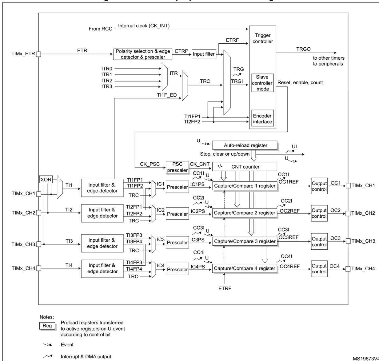
The diagram illustrates the internal architecture of a general-purpose timer. At the top, the 'Internal clock (CK_INT)' from the RCC is connected to the 'Trigger controller'. The 'ETR' (External Timer Register) input passes through a 'Polarity selection & edge detector & prescaler' to produce 'ETRP', which then goes through an 'Input filter' to become 'ETRF'. 'ETRF' is connected to the 'Trigger controller'. Four internal timer register (ITR) inputs (ITR0, ITR1, ITR2, ITR3) are combined via an 'XOR' gate to produce 'ITR', which is filtered to become 'TRC'. 'TRC' is also connected to the 'Trigger controller'. The 'TI1' input (derived from 'TIMx_CH1' through an 'XOR' gate) passes through an 'Input filter & edge detector' to produce 'TI1FP1' and 'TI1FP2'. These are captured by 'IC1', which is prescaled by 'IC1PS' to become 'CC1I'. 'CC1I' is connected to the 'Capture/Compare 1 register'. Similar paths exist for 'TI2' (producing 'IC2', 'IC2PS', 'CC2I'), 'TI3' (producing 'IC3', 'IC3PS', 'CC3I'), and 'TI4' (producing 'IC4', 'IC4PS', 'CC4I'). All 'CC' registers are connected to a central 'CNT counter'. The 'CNT counter' is also connected to an 'Auto-reload register' (with 'Stop, clear or up/down' control) and receives 'CK_CNT' from a 'PSC prescaler' (driven by 'CK_PSC'). The 'CNT counter' outputs are connected to 'Capture/Compare' registers, which then pass through 'Output control' blocks to produce 'OC1' (TIMx_CH1), 'OC2' (TIMx_CH2), 'OC3' (TIMx_CH3), and 'OC4' (TIMx_CH4). The 'Trigger controller' also connects to a 'Slave controller mode' and an 'Encoder interface'. The 'Slave controller mode' produces 'TRGO' to other peripherals and provides 'Reset, enable, count' signals. The 'Encoder interface' receives 'TI1FP1', 'TI1FP2', and 'TRC' inputs. A legend at the bottom left explains the symbols for registers, events, and interrupt & DMA outputs.
Notes:
[Reg] Preload registers transferred to active registers on U event according to control bit
⚡ Event
⚡ Interrupt & DMA output
MS19673V4
34.3 TIM2/TIM3/TIM4/TIM5 functional description
34.3.1 Time-base unit
The main block of the programmable timer is a 16-bit/32-bit counter with its related auto-reload register. The counter can count up, down or both up and down. The counter clock can be divided by a prescaler.
The counter, the auto-reload register and the prescaler register can be written or read by software. This is true even when the counter is running.
The time-base unit includes:
- • Counter Register (TIMx_CNT)
- • Prescaler Register (TIMx_PSC)
- • Auto-Reload Register (TIMx_ARR)
The auto-reload register is preloaded. Writing to or reading from the auto-reload register accesses the preload register. The content of the preload register are transferred into the shadow register permanently or at each update event (UEV), depending on the auto-reload preload enable bit (ARPE) in TIMx_CR1 register. The update event is sent when the counter reaches the overflow (or underflow when downcounting) and if the UDIS bit equals 0 in the TIMx_CR1 register. It can also be generated by software. The generation of the update event is described in detail for each configuration.
The counter is clocked by the prescaler output CK_CNT, which is enabled only when the counter enable bit (CEN) in TIMx_CR1 register is set (refer also to the slave mode controller description to get more details on counter enabling).
Note that the actual counter enable signal CNT_EN is set 1 clock cycle after CEN.
Prescaler description
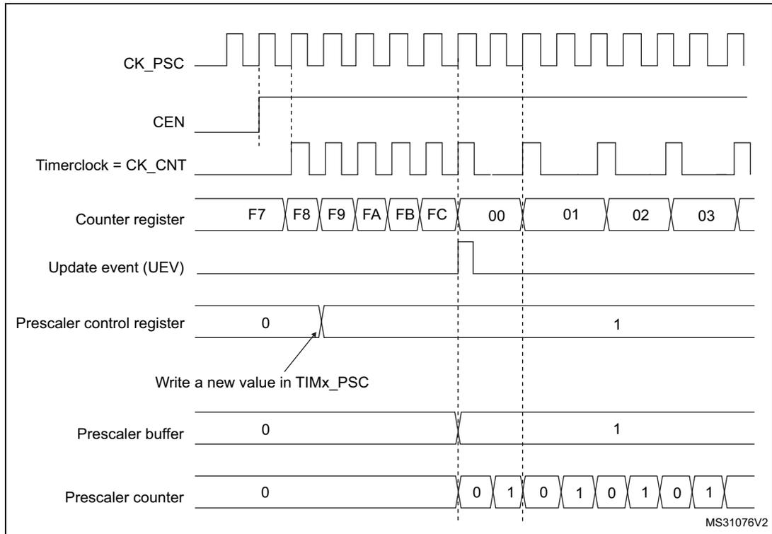
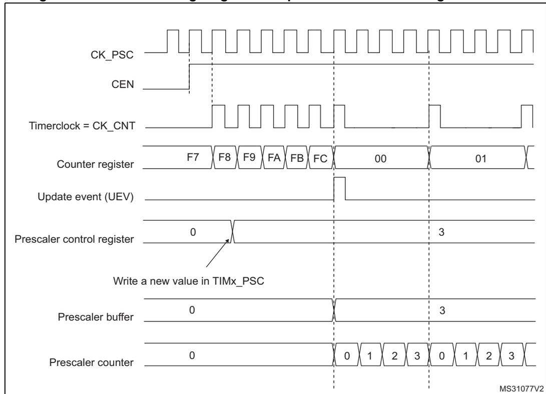
The prescaler can divide the counter clock frequency by any factor between 1 and 65536. It is based on a 16-bit counter controlled through a 16-bit/32-bit register (in the TIMx_PSC register). It can be changed on the fly as this control register is buffered. The new prescaler ratio is taken into account at the next update event.
Figure 292 and Figure 293 give some examples of the counter behavior when the prescaler ratio is changed on the fly:
Figure 292. Counter timing diagram with prescaler division change from 1 to 2
This timing diagram illustrates the behavior of a general-purpose timer when the prescaler division is changed from 1 to 2. The diagram shows the following signals and their states over time:
- CK_PSC : A periodic clock signal.
- CEN : Counter Enable signal, which is active low. It is shown as high (inactive) throughout the diagram.
- Timerclock = CK_CNT : The clock signal for the counter, which is derived from CK_PSC. Its frequency changes when the prescaler division changes.
- Counter register : Shows the count values. It starts at F7, increments through F8, F9, FA, FB, and FC. Upon reaching FC, it generates an Update Event (UEV) and resets to 00. The count then continues with 01, 02, and 03.
- Update event (UEV) : A pulse generated when the counter register overflows from FC to 00.
- Prescaler control register : Initially contains the value 0 (division by 1). At the time of the UEV, a new value of 1 (division by 2) is written to it.
- Write a new value in TIMx_PSC : An annotation indicating the write operation to the prescaler control register at the UEV.
- Prescaler buffer : A buffer that latches the value from the prescaler control register. It initially contains 0 and updates to 1 at the UEV.
- Prescaler counter : A counter that divides the CK_PSC frequency. It counts from 0 to 1 (when division is 2) and then resets. The diagram shows the sequence 0, 1, 0, 1, 0, 1, 0, 1 after the division change.
MS31076V2
Figure 293. Counter timing diagram with prescaler division change from 1 to 4
This timing diagram illustrates the behavior of a general-purpose timer when the prescaler division is changed from 1 to 4. The diagram shows the following signals and their states over time:
- CK_PSC : A periodic clock signal.
- CEN : Counter Enable signal, which is active low. It is shown as high (inactive) throughout the diagram.
- Timerclock = CK_CNT : The clock signal for the counter, which is derived from CK_PSC. Its frequency changes when the prescaler division changes.
- Counter register : Shows the count values. It starts at F7, increments through F8, F9, FA, FB, and FC. Upon reaching FC, it generates an Update Event (UEV) and resets to 00. The count then continues with 01.
- Update event (UEV) : A pulse generated when the counter register overflows from FC to 00.
- Prescaler control register : Initially contains the value 0 (division by 1). At the time of the UEV, a new value of 3 (division by 4) is written to it.
- Write a new value in TIMx_PSC : An annotation indicating the write operation to the prescaler control register at the UEV.
- Prescaler buffer : A buffer that latches the value from the prescaler control register. It initially contains 0 and updates to 3 at the UEV.
- Prescaler counter : A counter that divides the CK_PSC frequency. It counts from 0 to 3 (when division is 4) and then resets. The diagram shows the sequence 0, 1, 2, 3, 0, 1, 2, 3 after the division change.
MS31077V2
34.3.2 Counter modes
Upcounting mode
In upcounting mode, the counter counts from 0 to the auto-reload value (content of the TIMx_ARR register), then restarts from 0 and generates a counter overflow event.
An Update event can be generated at each counter overflow or by setting the UG bit in the TIMx_EGR register (by software or by using the slave mode controller).
The UEV event can be disabled by software by setting the UDIS bit in TIMx_CR1 register. This is to avoid updating the shadow registers while writing new values in the preload registers. Then no update event occurs until the UDIS bit has been written to 0. However, the counter restarts from 0, as well as the counter of the prescaler (but the prescale rate does not change). In addition, if the URS bit (update request selection) in TIMx_CR1 register is set, setting the UG bit generates an update event UEV but without setting the UIF flag (thus no interrupt or DMA request is sent). This is to avoid generating both update and capture interrupts when clearing the counter on the capture event.
When an update event occurs, all the registers are updated and the update flag (UIF bit in TIMx_SR register) is set (depending on the URS bit):
- • The buffer of the prescaler is reloaded with the preload value (content of the TIMx_PSC register)
- • The auto-reload shadow register is updated with the preload value (TIMx_ARR)
The following figures show some examples of the counter behavior for different clock frequencies when TIMx_ARR=0x36.
Figure 294. Counter timing diagram, internal clock divided by 1
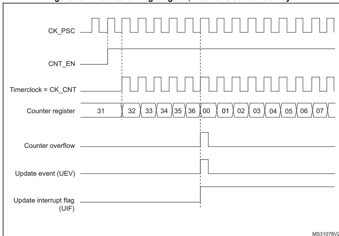
Timing diagram showing the relationship between the prescaler clock (CK_PSC), counter enable (CNT_EN), timer clock (Timerclock = CK_CNT), counter register values, counter overflow, update event (UEV), and update interrupt flag (UIF). The counter register values shown are 31, 32, 33, 34, 35, 36, 00, 01, 02, 03, 04, 05, 06, 07. The counter overflow and update event (UEV) occur when the counter reaches 36 and resets to 00. The update interrupt flag (UIF) is set at the same time as the overflow and UEV.
MS31078V2
Figure 295. Counter timing diagram, internal clock divided by 2
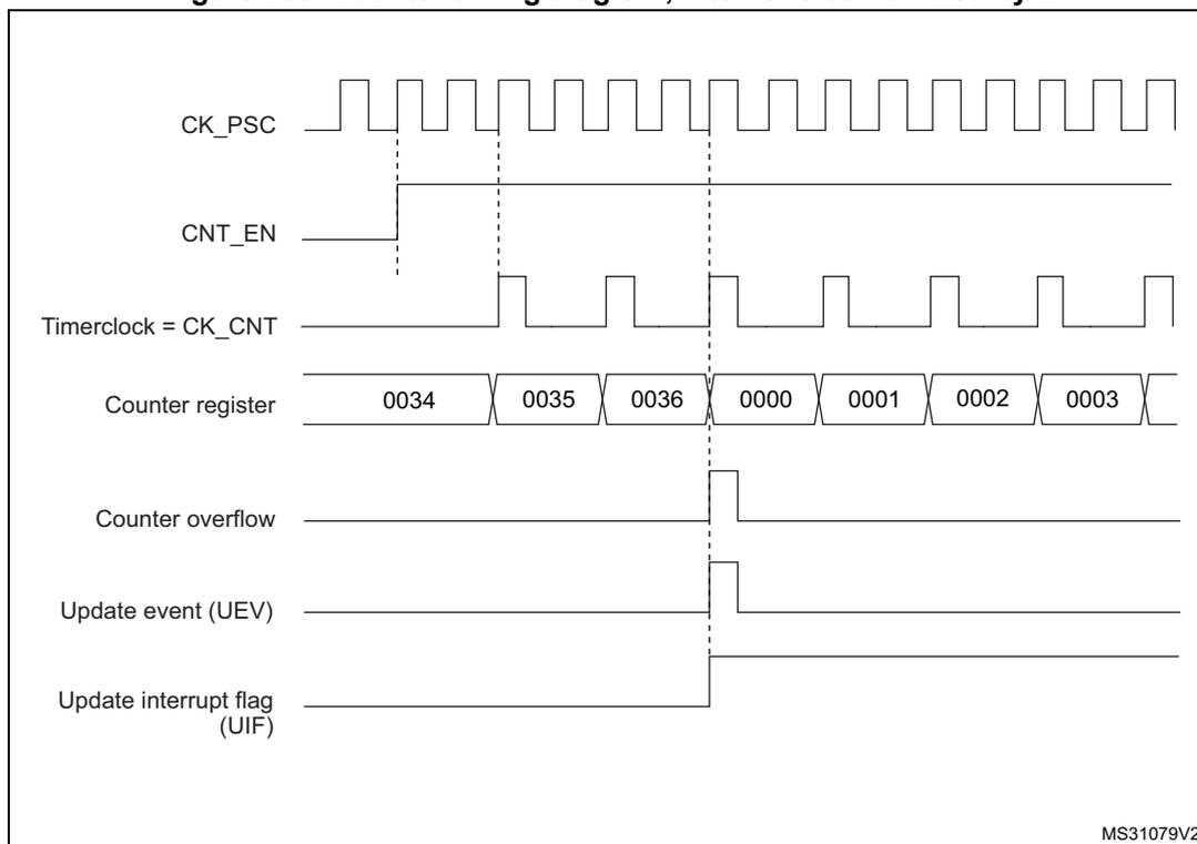
Timing diagram showing the relationship between the prescaler clock (CK_PSC), counter enable (CNT_EN), timer clock (CK_CNT), counter register values, counter overflow, update event (UEV), and update interrupt flag (UIF) when the internal clock is divided by 2.
The diagram illustrates the following signals and events:
- CK_PSC : Prescaler clock signal, shown as a square wave.
- CNT_EN : Counter enable signal, which goes high to start counting.
- Timerclock = CK_CNT : Counter clock signal, derived from CK_PSC and divided by 2.
- Counter register : Shows the sequence of values: 0034, 0035, 0036, 0000, 0001, 0002, 0003.
- Counter overflow : A pulse generated when the counter reaches 0036 and rolls over to 0000.
- Update event (UEV) : A pulse generated when the counter reaches 0036 and rolls over to 0000.
- Update interrupt flag (UIF) : A pulse generated when the counter reaches 0036 and rolls over to 0000.
MS31079V2
Figure 296. Counter timing diagram, internal clock divided by 4
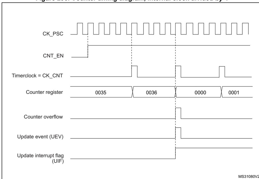
Timing diagram showing the relationship between the prescaler clock (CK_PSC), counter enable (CNT_EN), timer clock (CK_CNT), counter register values, counter overflow, update event (UEV), and update interrupt flag (UIF) when the internal clock is divided by 4.
The diagram illustrates the following signals and events:
- CK_PSC : Prescaler clock signal, shown as a square wave.
- CNT_EN : Counter enable signal, which goes high to start counting.
- Timerclock = CK_CNT : Counter clock signal, derived from CK_PSC and divided by 4.
- Counter register : Shows the sequence of values: 0035, 0036, 0000, 0001.
- Counter overflow : A pulse generated when the counter reaches 0036 and rolls over to 0000.
- Update event (UEV) : A pulse generated when the counter reaches 0036 and rolls over to 0000.
- Update interrupt flag (UIF) : A pulse generated when the counter reaches 0036 and rolls over to 0000.
MS31080V2
Figure 297. Counter timing diagram, internal clock divided by N
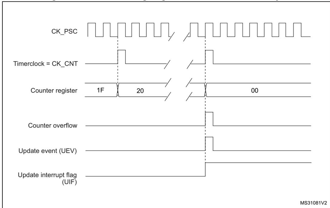
This timing diagram illustrates the operation of a timer when the internal clock is divided by N. The top signal, CK_PSC, is a periodic square wave. Below it, Timerclock = CK_CNT is shown as a series of pulses derived from CK_PSC. The Counter register is shown with values 1F, 20, and 00. A Counter overflow pulse occurs when the counter reaches 20. The Update event (UEV) is a pulse that coincides with the overflow. The Update interrupt flag (UIF) is a signal that goes high at the overflow and remains high until cleared.
MS31081V2
Figure 298. Counter timing diagram, Update event when ARPE=0 (TIMx_ARR not preloaded)
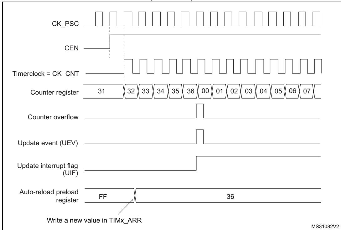
This timing diagram shows the timer's behavior when ARPE=0 and the auto-reload register is not preloaded. The signals shown are CK_PSC, CEN (counter enable), Timerclock = CK_CNT, Counter register, Counter overflow, Update event (UEV), Update interrupt flag (UIF), and the Auto-reload preload register. The counter starts at 31 and increments through 32, 33, 34, 35, 36, 00, 01, 02, 03, 04, 05, 06, 07. A Counter overflow pulse occurs at 36. The Update event (UEV) is a pulse that coincides with the overflow. The Update interrupt flag (UIF) is a signal that goes high at the overflow. The Auto-reload preload register is shown with values FF and 36. A note indicates that writing a new value in TIMx_ARR occurs at the overflow.
MS31082V2
Figure 299. Counter timing diagram, Update event when ARPE=1 (TIMx_ARR preloaded)
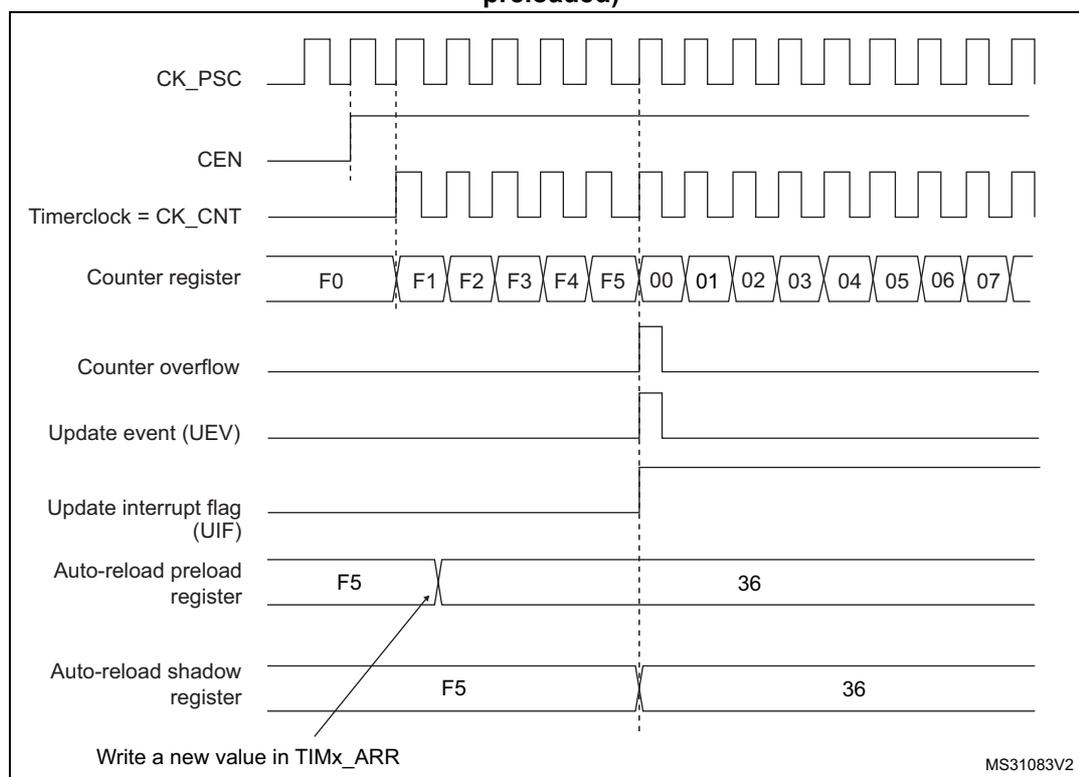
The timing diagram illustrates the operation of a general-purpose timer in upcounting mode with ARPE=1. The signals shown are:
- CK_PSC : Prescaler clock signal, shown as a square wave.
- CEN : Counter enable signal, which goes high to enable counting.
- Timerclock = CK_CNT : Counter clock signal, derived from CK_PSC.
- Counter register : Shows the counter values: F0, F1, F2, F3, F4, F5, 00, 01, 02, 03, 04, 05, 06, 07. The counter increments from F0 to F5, then overflows to 00.
- Counter overflow : A pulse generated when the counter reaches 00.
- Update event (UEV) : A pulse generated when the counter overflows.
- Update interrupt flag (UIF) : A pulse generated when the counter overflows.
- Auto-reload preload register : Shows the value F5 being written, then 36 being loaded into the register.
- Auto-reload shadow register : Shows the value F5 being written, then 36 being loaded into the shadow register.
An arrow indicates that a new value (36) is written in the TIMx_ARR register after the counter reaches F5. The diagram is labeled MS31083V2.
Downcounting mode
In downcounting mode, the counter counts from the auto-reload value (content of the TIMx_ARR register) down to 0, then restarts from the auto-reload value and generates a counter underflow event.
An Update event can be generated at each counter underflow or by setting the UG bit in the TIMx_EGR register (by software or by using the slave mode controller).
The UEV update event can be disabled by software by setting the UDIS bit in TIMx_CR1 register. This is to avoid updating the shadow registers while writing new values in the preload registers. Then no update event occurs until UDIS bit has been written to 0. However, the counter restarts from the current auto-reload value, whereas the counter of the prescaler restarts from 0 (but the prescale rate doesn't change).
In addition, if the URS bit (update request selection) in TIMx_CR1 register is set, setting the UG bit generates an update event UEV but without setting the UIF flag (thus no interrupt or DMA request is sent). This is to avoid generating both update and capture interrupts when clearing the counter on the capture event.
When an update event occurs, all the registers are updated and the update flag (UIF bit in TIMx_SR register) is set (depending on the URS bit):
- • The buffer of the prescaler is reloaded with the preload value (content of the TIMx_PSC register).
- • The auto-reload active register is updated with the preload value (content of the TIMx_ARR register). Note that the auto-reload is updated before the counter is reloaded, so that the next period is the expected one.
The following figures show some examples of the counter behavior for different clock frequencies when TIMx_ARR=0x36.
Figure 300. Counter timing diagram, internal clock divided by 1
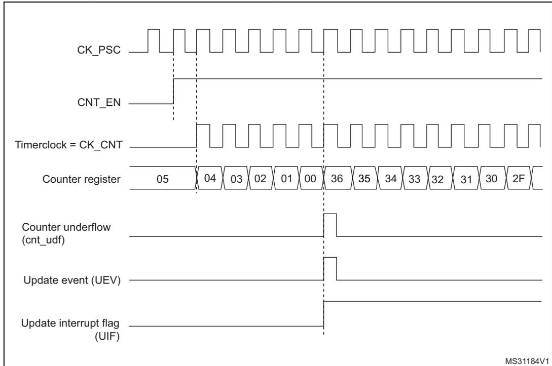
This timing diagram illustrates the counter behavior when the internal clock is divided by 1. The signals shown are:
- CK_PSC : Prescaler clock signal, a periodic square wave.
- CNT_EN : Counter enable signal, which goes high to start counting.
- Timerclock = CK_CNT : The clock signal for the counter, which is the output of the prescaler.
- Counter register : Shows the sequence of values: 05, 04, 03, 02, 01, 00, 36, 35, 34, 33, 32, 31, 30, 2F. The values decrease by 1 at each rising edge of the timer clock until they reach 00, at which point they roll over to 36 (0x36).
- Counter underflow (cnt_udf) : A pulse that goes high when the counter reaches 00 and rolls over to 36.
- Update event (UEV) : A pulse that goes high when the counter reaches 00.
- Update interrupt flag (UIF) : A signal that goes high when the counter reaches 00 and remains high until it is cleared.
Vertical dashed lines indicate the timing of the counter register updates and the generation of the underflow, update event, and interrupt flag.
MS31184V1
Figure 301. Counter timing diagram, internal clock divided by 2
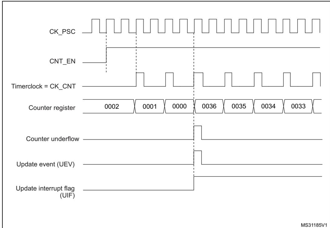
This timing diagram illustrates the counter behavior when the internal clock is divided by 2. The signals shown are:
- CK_PSC : Prescaler clock signal, a periodic square wave.
- CNT_EN : Counter enable signal, which goes high to start counting.
- Timerclock = CK_CNT : The clock signal for the counter, which is half the frequency of the prescaler output.
- Counter register : Shows the sequence of values: 0002, 0001, 0000, 0036, 0035, 0034, 0033. The values decrease by 1 at each rising edge of the timer clock until they reach 0000, at which point they roll over to 0036 (0x36).
- Counter underflow : A pulse that goes high when the counter reaches 0000 and rolls over to 0036.
- Update event (UEV) : A pulse that goes high when the counter reaches 0000.
- Update interrupt flag (UIF) : A signal that goes high when the counter reaches 0000 and remains high until it is cleared.
Vertical dashed lines indicate the timing of the counter register updates and the generation of the underflow, update event, and interrupt flag.
MS31185V1
Figure 302. Counter timing diagram, internal clock divided by 4
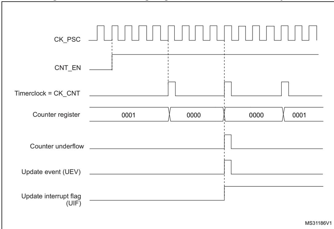
This timing diagram illustrates the operation of a timer when the internal clock is divided by 4. The top signal, CK_PSC, is a periodic square wave. The CNT_EN signal is a horizontal line that goes high to enable the counter. The Timerclock = CK_CNT signal is a square wave that is active only when CNT_EN is high. The Counter register shows a sequence of values: 0001, 0000, 0000, and 0001. The Counter underflow signal is a pulse that occurs when the counter reaches 0000. The Update event (UEV) and Update interrupt flag (UIF) are also shown as pulses that occur when the counter reaches 0000. The diagram is labeled MS31186V1 in the bottom right corner.
Figure 303. Counter timing diagram, internal clock divided by N
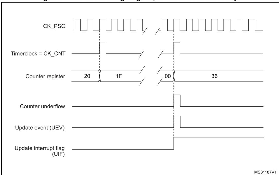
This timing diagram illustrates the operation of a timer when the internal clock is divided by N. The top signal, CK_PSC, is a periodic square wave. The Timerclock = CK_CNT signal is a square wave that is active only when CNT_EN is high. The Counter register shows a sequence of values: 20, 1F, 00, and 36. The Counter underflow signal is a pulse that occurs when the counter reaches 00. The Update event (UEV) and Update interrupt flag (UIF) are also shown as pulses that occur when the counter reaches 00. The diagram is labeled MS31187V1 in the bottom right corner.
Figure 304. Counter timing diagram, Update event
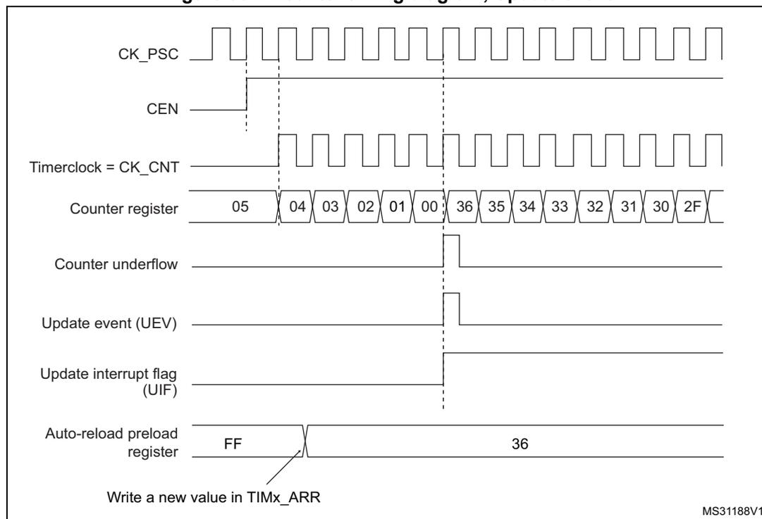
The timing diagram illustrates the operation of a general-purpose timer. The top signal, CK_PSC, is a periodic clock. Below it, CEN (Counter Enable) is shown as a high-level signal. The third signal, Timerclock = CK_CNT, is a divided version of CK_PSC. The fourth signal shows the Counter register values, which are 05, 04, 03, 02, 01, 00, 36, 35, 34, 33, 32, 31, 30, and 2F. The fifth signal, Counter underflow, is a pulse that goes high when the counter reaches 00. The sixth signal, Update event (UEV), is a pulse that goes high when the counter reaches 00. The seventh signal, Update interrupt flag (UIF), is a pulse that goes high when the counter reaches 00. The eighth signal, Auto-reload preload register, shows the values FF and 36. A note indicates that a new value can be written in TIMx_ARR.
Center-aligned mode (up/down counting)
In center-aligned mode, the counter counts from 0 to the auto-reload value (content of the TIMx_ARR register) – 1, generates a counter overflow event, then counts from the auto-reload value down to 1 and generates a counter underflow event. Then it restarts counting from 0.
Center-aligned mode is active when the CMS bits in TIMx_CR1 register are not equal to '00'. The Output compare interrupt flag of channels configured in output is set when: the counter counts down (Center aligned mode 1, CMS = "01"), the counter counts up (Center aligned mode 2, CMS = "10") the counter counts up and down (Center aligned mode 3, CMS = "11").
In this mode, the direction bit (DIR from TIMx_CR1 register) cannot be written. It is updated by hardware and gives the current direction of the counter.
The update event can be generated at each counter overflow and at each counter underflow or by setting the UG bit in the TIMx_EGR register (by software or by using the slave mode controller) also generates an update event. In this case, the counter restarts counting from 0, as well as the counter of the prescaler.
The UEV update event can be disabled by software by setting the UDIS bit in TIMx_CR1 register. This is to avoid updating the shadow registers while writing new values in the preload registers. Then no update event occurs until the UDIS bit has been written to 0. However, the counter continues counting up and down, based on the current auto-reload value.
In addition, if the URS bit (update request selection) in TIMx_CR1 register is set, setting the UG bit generates an update event UEV but without setting the UIF flag (thus no interrupt or
DMA request is sent). This is to avoid generating both update and capture interrupt when clearing the counter on the capture event.
When an update event occurs, all the registers are updated and the update flag (UIF bit in TIMx_SR register) is set (depending on the URS bit):
- • The buffer of the prescaler is reloaded with the preload value (content of the TIMx_PSC register).
- • The auto-reload active register is updated with the preload value (content of the TIMx_ARR register). Note that if the update source is a counter overflow, the auto-reload is updated before the counter is reloaded, so that the next period is the expected one (the counter is loaded with the new value).
The following figures show some examples of the counter behavior for different clock frequencies.
Figure 305. Counter timing diagram, internal clock divided by 1, TIMx_ARR=0x6
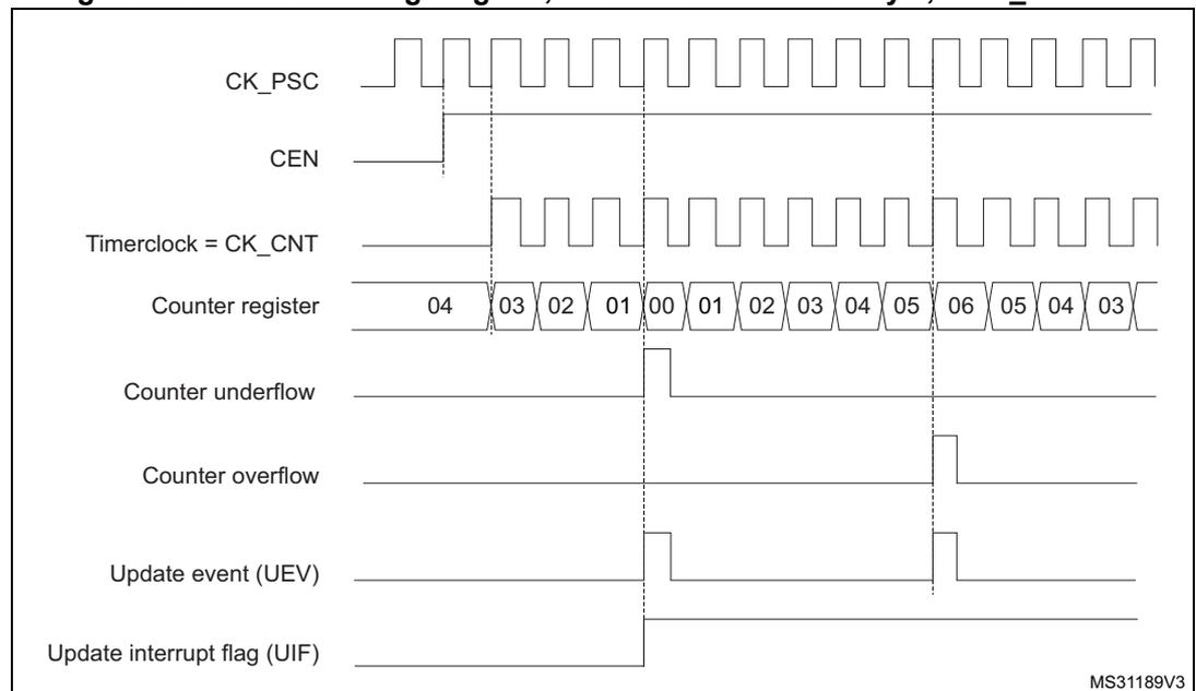
The timing diagram illustrates the counter's behavior over time. The top signal, CK_PSC, is a periodic square wave. Below it, CEN is a horizontal line that goes high to enable the timer. The Timerclock = CK_CNT signal is a square wave that is half the frequency of CK_PSC. The Counter register shows a sequence of values: 04, 03, 02, 01, 00, 01, 02, 03, 04, 05, 06, 05, 04, 03. Vertical dashed lines mark key events: a counter underflow occurs when the counter reaches 00 and a counter overflow occurs when it reaches 06. The Update event (UEV) is a pulse that occurs at both underflow and overflow. The Update interrupt flag (UIF) is a pulse that goes high at the underflow event and returns low at the overflow event. The diagram is labeled MS31189V3 in the bottom right corner.
- 1. Here, center-aligned mode 1 is used (for more details refer to Section 34.4.1: TIMx control register 1 (TIMx_CR1)(x = 2 to 5) on page 1223 ).
Figure 306. Counter timing diagram, internal clock divided by 2
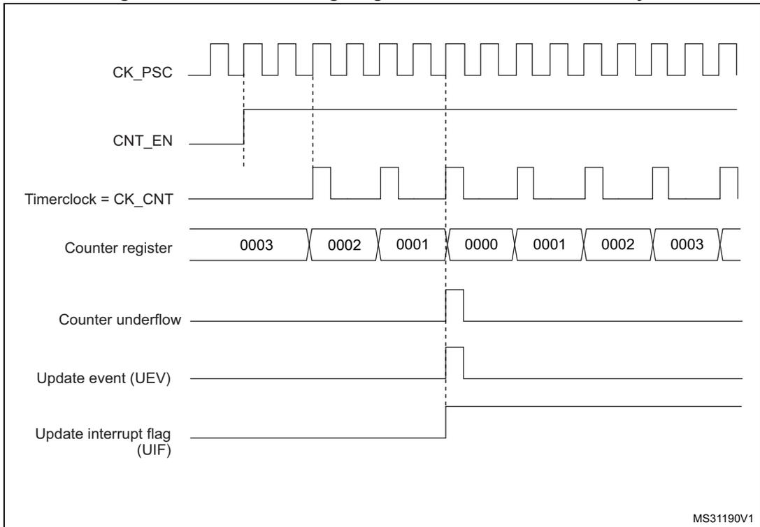
This timing diagram illustrates the operation of a timer with the internal clock divided by 2. The top signal, CK_PSC, is a periodic square wave. Below it, CNT_EN is a high-level enable signal. The Timerclock = CK_CNT signal is a square wave with a frequency half that of CK_PSC. The Counter register shows a sequence of values: 0003, 0002, 0001, 0000, 0001, 0002, 0003. Vertical dashed lines indicate key timing points: the first at the rising edge of CK_PSC when the counter reaches 0000; the second at the next rising edge of CK_PSC when the counter reaches 0001; and the third at the rising edge of CK_CNT when the counter reaches 0000. At the third dashed line, the Counter underflow, Update event (UEV), and Update interrupt flag (UIF) signals all go high. The UIF signal remains high until the next rising edge of CK_CNT.
MS31190V1
Figure 307. Counter timing diagram, internal clock divided by 4, TIMx_ARR=0x36
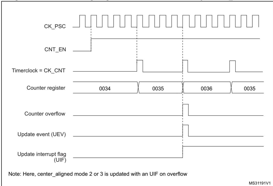
This timing diagram shows the timer operation with the internal clock divided by 4 and an auto-reload register value of 0x36. The signals CK_PSC, CNT_EN, and Timerclock = CK_CNT are similar to Figure 306, but the Timerclock frequency is one-quarter of the CK_PSC frequency. The Counter register values shown are 0034, 0035, 0036, and 0035. Vertical dashed lines mark specific events: the first at the rising edge of CK_PSC when the counter reaches 0036; the second at the next rising edge of CK_PSC when the counter reaches 0035; and the third at the rising edge of CK_CNT when the counter reaches 0036. At the third dashed line, the Counter overflow, Update event (UEV), and Update interrupt flag (UIF) signals all go high. The UIF signal remains high until the next rising edge of CK_CNT.
Note: Here, center_aligned mode 2 or 3 is updated with an UIF on overflow
MS31190V1
- 1. Center-aligned mode 2 or 3 is used with an UIF on overflow.
Figure 308. Counter timing diagram, internal clock divided by N
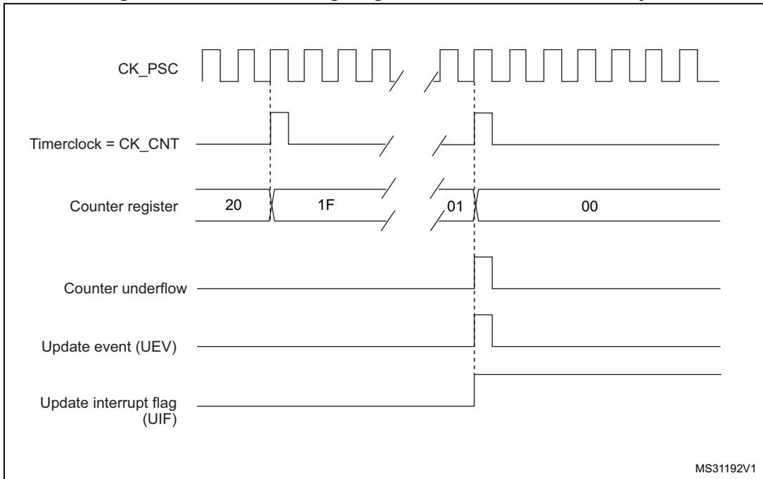
The diagram illustrates the timing of a counter when the internal clock is divided by N. The top signal is CK_PSC, a periodic square wave. Below it is Timerclock = CK_CNT, which is a pulse that occurs on the rising edge of CK_PSC. The Counter register shows a sequence of values: 20, 1F, 01, 00. The Counter underflow signal is a pulse that occurs when the counter register reaches 00. The Update event (UEV) signal is a pulse that occurs when the counter register reaches 00. The Update interrupt flag (UIF) signal is a pulse that occurs when the counter register reaches 00. The diagram is labeled MS31192V1.
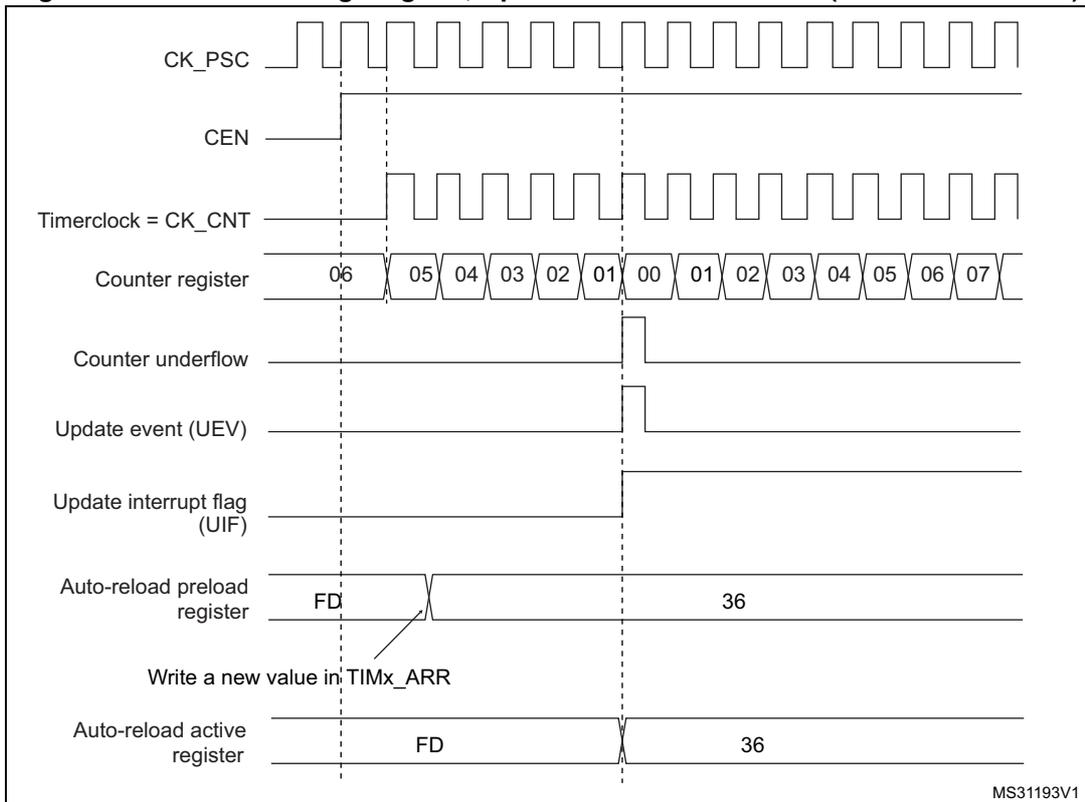
Figure 309. Counter timing diagram, Update event with ARPE=1 (counter underflow)
The diagram illustrates the timing of a counter when the Update event is generated by a counter underflow and ARPE=1. The top signal is CK_PSC, a periodic square wave. Below it is CEN, which is a pulse that enables the counter. The Timerclock = CK_CNT signal is a pulse that occurs on the rising edge of CK_PSC. The Counter register shows a sequence of values: 06, 05, 04, 03, 02, 01, 00, 01, 02, 03, 04, 05, 06, 07. The Counter underflow signal is a pulse that occurs when the counter register reaches 00. The Update event (UEV) signal is a pulse that occurs when the counter register reaches 00. The Update interrupt flag (UIF) signal is a pulse that occurs when the counter register reaches 00. The Auto-reload preload register shows values FD and 36. The Write a new value in TIMx_ARR signal is shown as a pulse. The Auto-reload active register shows values FD and 36. The diagram is labeled MS31193V1.
Figure 310. Counter timing diagram, Update event with ARPE=1 (counter overflow)
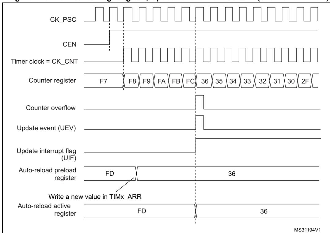
The timing diagram illustrates the behavior of a general-purpose timer when an update event is generated by a counter overflow with ARPE=1. The signals shown are:
- CK_PSC : Prescaler clock, a periodic square wave.
- CEN : Counter enable, which goes high to start the counter.
- Timer clock = CK_CNT : The clock driving the counter, derived from CK_PSC.
- Counter register : Shows the count values. It starts at F7, increments through F8, F9, FA, FB, FC, then overflows to 36, and continues with 35, 34, 33, 32, 31, 30, 2F.
- Counter overflow : A pulse generated when the counter reaches its maximum value (FC) and overflows to 36.
- Update event (UEV) : A pulse generated when the counter overflows.
- Update interrupt flag (UIF) : A flag that is set when an update event occurs.
- Auto-reload preload register : Shows the value FD being updated to 36 at the time of the update event.
- Write a new value in TIMx_ARR : The software write to the auto-reload register.
- Auto-reload active register : Shows the value FD being updated to 36 at the time of the update event.
MS31194V1
34.3.3 Clock selection
The counter clock can be provided by the following clock sources:
- • Internal clock (CK_INT)
- • External clock mode1: external input pin (TIx)
- • External clock mode2: external trigger input (ETR)
- • Internal trigger inputs (ITRx): using one timer as prescaler for another timer, for example, Timer X can be configured to act as a prescaler for Timer Y. Refer to : Using one timer as prescaler for another timer on page 1217 for more details.
Internal clock source (CK_INT)
If the slave mode controller is disabled (SMS=000 in the TIMx_SMCR register), then the CEN, DIR (in the TIMx_CR1 register) and UG bits (in the TIMx_EGR register) are actual control bits and can be changed only by software (except UG which remains cleared automatically). As soon as the CEN bit is written to 1, the prescaler is clocked by the internal clock CK_INT.
Figure 311 shows the behavior of the control circuit and the upcounter in normal mode, without prescaler.
Figure 311. Control circuit in normal mode, internal clock divided by 1
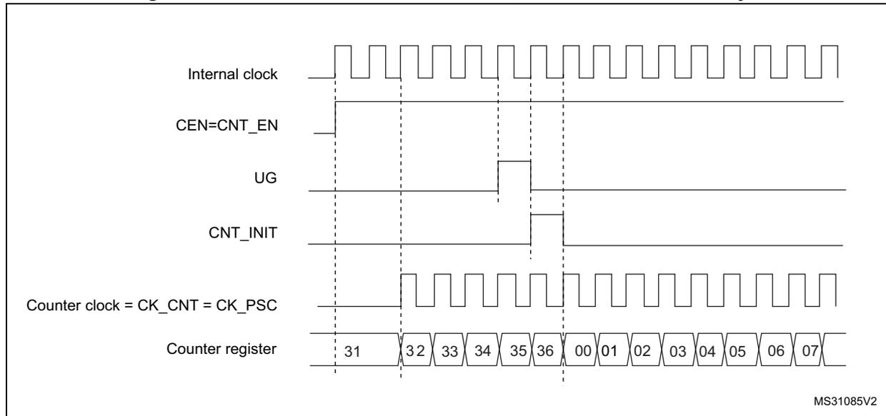
The diagram shows the timing relationship between several signals and the counter register. The 'Internal clock' is a continuous square wave. The 'CEN=CNT_EN' signal is a horizontal line that goes high at the start. The 'UG' (Update Generation) signal is a pulse that goes high when the counter reaches 36 and returns low at 00. The 'CNT_INIT' signal is a pulse that goes high at 36 and returns low at 01. The 'Counter clock = CK_CNT = CK_PSC' is a square wave that starts at 32 and is active when CEN is high. The 'Counter register' shows a sequence of values: 31, 32, 33, 34, 35, 36, 00, 01, 02, 03, 04, 05, 06, 07. Vertical dashed lines indicate the clock edges corresponding to the counter value changes.
MS31085V2
External clock source mode 1
This mode is selected when SMS=111 in the TIMx_SMCR register. The counter can count at each rising or falling edge on a selected input.
Figure 312. TI2 external clock connection example
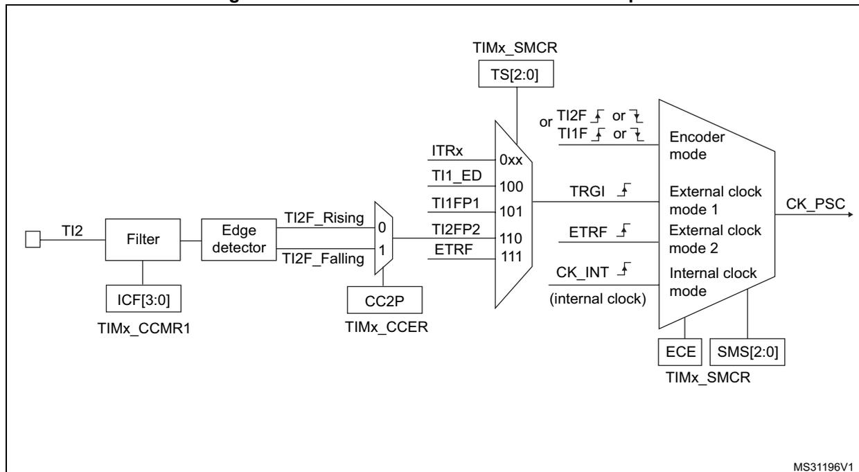
The diagram illustrates the connection of the TI2 input to the external clock source. The TI2 input passes through a 'Filter' block (controlled by ICF[3:0] in TIMx_CCMR1) and an 'Edge detector' block (controlled by CC2P in TIMx_CCER). The edge detector outputs 'TI2F_Rising' and 'TI2F_Falling' signals. These signals are multiplexed (0 for rising, 1 for falling) and then connected to a 'TIMx_SMCR' register block. The 'TIMx_SMCR' register contains several fields: 'TS[2:0]' (0xx), 'ITRx' (0xx), 'TI1_ED' (100), 'TI1FP1' (101), 'TI2FP2' (110), and 'ETR' (111). The 'TI2F_Rising' and 'TI2F_Falling' signals are connected to the 'TRGI' input of the 'Encoder mode' block. The 'Encoder mode' block also receives 'CK_INT' (internal clock) and 'ETR' signals. The output of the 'Encoder mode' block is 'CK_PSC'. The 'TIMx_SMCR' register also contains 'ECE' and 'SMS[2:0]' fields, which are connected to the 'Encoder mode' block.
MS31196V1
For example, to configure the upcounter to count in response to a rising edge on the TI2 input, use the following procedure:
- 1. Configure channel 2 to detect rising edges on the TI2 input by writing CC2S= '01 in the TIMx_CCMR1 register.
- 2. Configure the input filter duration by writing the IC2F[3:0] bits in the TIMx_CCMR1 register (if no filter is needed, keep IC2F=0000).
Note: The capture prescaler is not used for triggering, so it does not need to be configured.
- 3. Select rising edge polarity by writing CC2P=0 and CC2NP=0 and CC2NP=0 in the TIMx_CCER register.
- 4. Configure the timer in external clock mode 1 by writing SMS=111 in the TIMx_SMCR register.
- 5. Select TI2 as the input source by writing TS=110 in the TIMx_SMCR register.
- 6. Enable the counter by writing CEN=1 in the TIMx_CR1 register.
When a rising edge occurs on TI2, the counter counts once and the TIF flag is set.
The delay between the rising edge on TI2 and the actual clock of the counter is due to the resynchronization circuit on TI2 input.
Figure 313. Control circuit in external clock mode 1
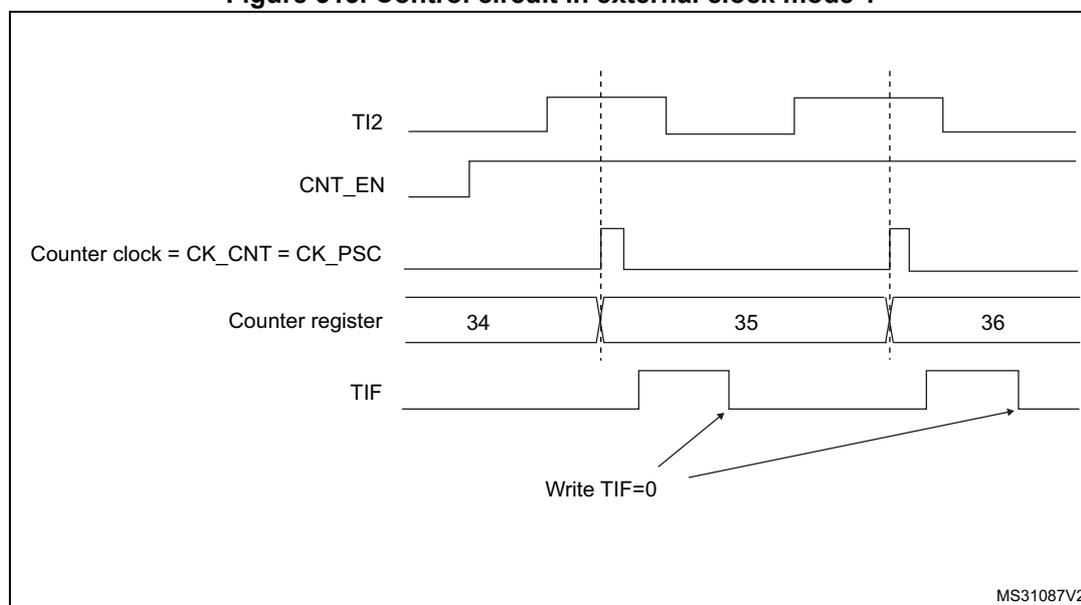
The diagram illustrates the timing for external clock mode 1. It shows five horizontal signal lines over time. The top line, labeled 'TI2', shows a periodic square wave. The second line, 'CNT_EN', is a signal that goes high and stays high. The third line, 'Counter clock = CK_CNT = CK_PSC', shows pulses that occur on the rising edges of the TI2 signal. The fourth line, 'Counter register', shows the count values 34, 35, and 36, which increment at each rising edge of the TI2 signal. The bottom line, 'TIF', shows a pulse that goes high when the counter increments and returns to zero when it is manually cleared. Two arrows labeled 'Write TIF=0' point to the falling edges of the TIF signal. The diagram is labeled 'MS31087V2' in the bottom right corner.
External clock source mode 2
This mode is selected by writing ECE=1 in the TIMx_SMCR register.
The counter can count at each rising or falling edge on the external trigger input ETR.
Figure 314 gives an overview of the external trigger input block.
Figure 314. External trigger input block
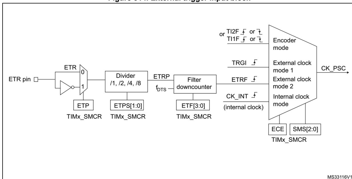
The diagram illustrates the external trigger input block for general-purpose timers. The signal flow is as follows:
- The ETR pin is connected to a multiplexer (MUX) labeled ETR . The MUX has two inputs: 0 (direct connection) and 1 (inverted connection). The output of the MUX is connected to a Divider block with options /1, /2, /4, /8 .
- The Divider block is controlled by the ETPS[1:0] register in TIMx_SMCR . Its output is ETRP .
- The ETRP signal is then processed by a Filter downcounter block. This block is controlled by the ETF[3:0] register in TIMx_SMCR . Its output is ETRF .
- The ETRF signal is then connected to a multiplexer for Encoder mode , External clock mode 1 , and External clock mode 2 . This multiplexer is controlled by the ECE and SMS[2:0] registers in TIMx_SMCR . The output of this multiplexer is CK_PSC .
- There are also other inputs to the Encoder mode multiplexer: TI2F or TI1F (with rising or falling edge symbols), TRGI (with rising edge symbol), and CK_INT (internal clock, with rising edge symbol).
- Additional control registers shown include ETP in TIMx_SMCR for the initial MUX selection.
MS33116V1
For example, to configure the upcounter to count each 2 rising edges on ETR, use the following procedure:
- 1. As no filter is needed in this example, write ETF[3:0]=0000 in the TIMx_SMCR register.
- 2. Set the prescaler by writing ETPS[1:0]=01 in the TIMx_SMCR register
- 3. Select rising edge detection on the ETR pin by writing ETP=0 in the TIMx_SMCR register
- 4. Enable external clock mode 2 by writing ECE=1 in the TIMx_SMCR register.
- 5. Enable the counter by writing CEN=1 in the TIMx_CR1 register.
The counter counts once each 2 ETR rising edges.
The delay between the rising edge on ETR and the actual clock of the counter is due to the resynchronization circuit on the ETRP signal. As a consequence, the maximum frequency which can be correctly captured by the counter is at most 1/4 of TIMxCLK frequency. When the ETRP signal is faster, the user should apply a division of the external signal by a proper ETPS prescaler setting.
Figure 315. Control circuit in external clock mode 2
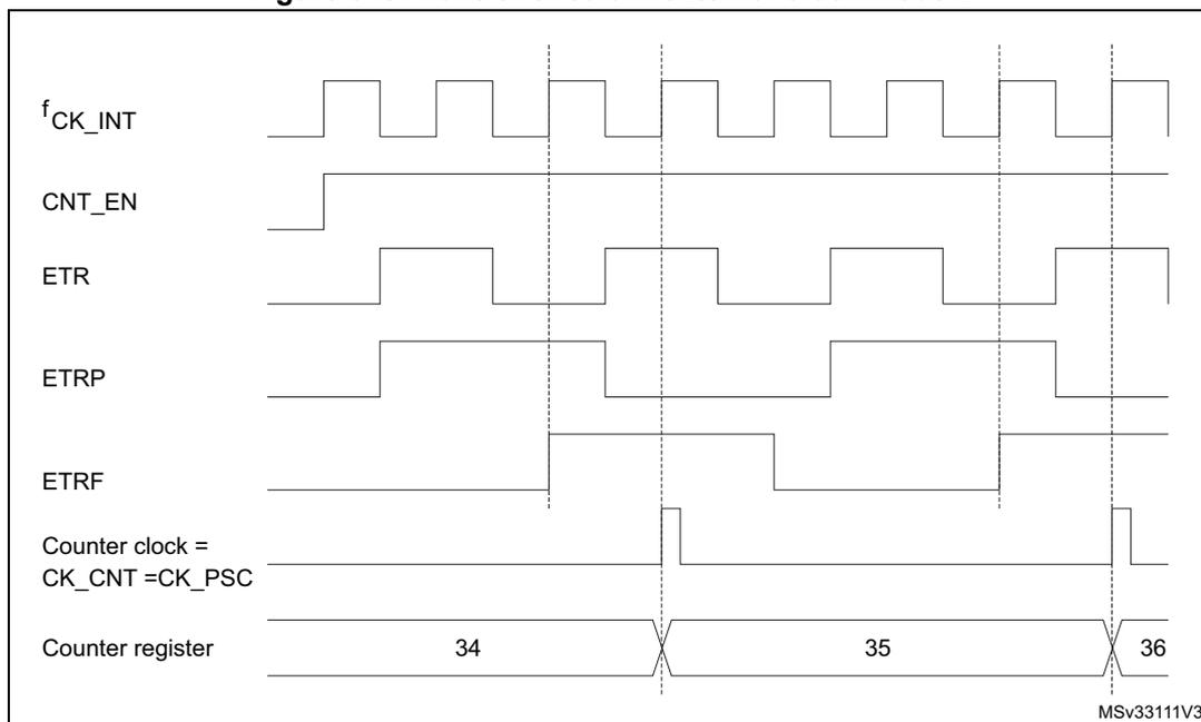
The timing diagram illustrates the control circuit in external clock mode 2. It shows the following signals and their relationship to the counter register values:
- f CK_INT : Internal clock frequency, shown as a periodic square wave.
- CNT_EN : Counter enable signal, shown as a high-level signal.
- ETR : External trigger input, shown as a square wave.
- ETRP : External trigger prescaler output, shown as a square wave with a lower frequency than ETR.
- ETRF : External trigger filter output, shown as a square wave with a lower frequency than ETRP.
- Counter clock = CK_CNT = CK_PSC : The clock signal for the counter, shown as a square wave with a frequency equal to f CK_INT .
- Counter register : The register that counts the number of clock cycles. It shows values 34, 35, and 36, with a break in the sequence between 34 and 35.
The diagram is labeled MSV3311V3 in the bottom right corner.
34.3.4 Capture/Compare channels
Each Capture/Compare channel is built around a capture/compare register (including a shadow register), a input stage for capture (with digital filter, multiplexing and prescaler) and an output stage (with comparator and output control).
The following figure gives an overview of one Capture/Compare channel.
The input stage samples the corresponding TIx input to generate a filtered signal TIxF. Then, an edge detector with polarity selection generates a signal (TIxFPx) which can be used as trigger input by the slave mode controller or as the capture command. It is prescaled before the capture register (ICxPS).
Figure 316. Capture/Compare channel (example: channel 1 input stage)
![Figure 316: Capture/Compare channel (example: channel 1 input stage) block diagram. The diagram shows the input stage for channel 1. TI1 is filtered by a downcounter (f_DTS) to produce TI1F. This is then processed by an edge detector to produce TI1F_Rising and TI1F_Falling signals. These signals are multiplexed with TI2F_Rising and TI2F_Falling (from channel 2) to produce TI1FP1 and TI2FP1. TI1FP1 is ANDed with TRC (from slave mode controller) to produce TI1F_ED, which is sent to the slave mode controller. TI2FP1 is used as IC1. IC1 is divided by a divider (/1, /2, /4, /8) to produce IC1PS. Control registers ICF[3:0] (TIMx_CCMR1), CC1P/CC1NP (TIMx_CCER), CC1S[1:0] (TIMx_CCMR1), ICPS[1:0] (TIMx_CCMR1), and CC1E (TIMx_CCER) are shown.](/RM0438-STM32L5/2bfbee9fba774c757bbc9e143710f777_img.jpg)
The output stage generates an intermediate waveform which is then used for reference: OCxRef (active high). The polarity acts at the end of the chain.
Figure 317. Capture/Compare channel 1 main circuit
![Figure 317: Capture/Compare channel 1 main circuit block diagram. The diagram shows the main circuit for channel 1. It is connected to an APB Bus via an MCU-peripheral interface. The interface provides a 16/32-bit signal to a Capture/compare preload register. This register is connected to a compare shadow register, which is in turn connected to a Counter. The Counter output is compared with CCR1 in a Comparator to produce CNT>CCR1 and CNT=CCR1 signals. The circuit is divided into Input mode and Output mode. In Input mode, CC1S[1], CC1S[0], IC1PS, CC1E, and CC1G (TIMx_EGR) are used to control the capture process. In Output mode, CC1S[1], CC1S[0], OC1PE, and UEV (from time base unit) are used to control the output process. Control registers CC1S[1], CC1S[0], OC1PE, and TIMx_CCMR1 are shown.](/RM0438-STM32L5/d09ddd7a3a9083ae2c989058ba055ac7_img.jpg)
Figure 318. Output stage of Capture/Compare channel (channel 1)
![Figure 318. Output stage of Capture/Compare channel (channel 1). The diagram shows the internal logic of the output stage. It starts with an 'Output mode controller' block that receives inputs 'CNT > CCR1', 'CNT = CCR1', and 'ETRF'. It has two outputs: 'OC1REF' and 'OC2REF'. 'OC1REF' is connected to an 'Output selector' block. 'OC2REF' is connected to a register block labeled 'OC1CE OC1M[3:0] TIMx_CCMR1'. The 'Output selector' block also receives 'OC1REFC' and a '0' input. Its output is connected to a multiplexer. This multiplexer has inputs '0' and '1', and is controlled by 'CC1E' and 'TIMx_CCER'. The output of this multiplexer is connected to an inverter. The output of the inverter is connected to another multiplexer. This second multiplexer has inputs '0' and '1', and is controlled by 'CC1P' and 'TIMx_CCER'. The output of this second multiplexer is connected to an 'Output enable circuit' block. This block also receives 'CC1E' and 'TIMx_CCER' inputs. The final output is 'OC1'. A label 'To the master mode controller' is at the top right. A label 'MSv40929V5' is at the bottom right.](/RM0438-STM32L5/83e9295b9d5753b8eecd41afb92a6ef5_img.jpg)
The capture/compare block is made of one preload register and one shadow register. Write and read always access the preload register.
In capture mode, captures are actually done in the shadow register, which is copied into the preload register.
In compare mode, the content of the preload register is copied into the shadow register which is compared to the counter.
34.3.5 Input capture mode
In Input capture mode, the Capture/Compare Registers (TIMx_CCRx) are used to latch the value of the counter after a transition detected by the corresponding ICx signal. When a capture occurs, the corresponding CCxIF flag (TIMx_SR register) is set and an interrupt or a DMA request can be sent if they are enabled. If a capture occurs while the CCxIF flag was already high, then the over-capture flag CCxOF (TIMx_SR register) is set. CCxIF can be cleared by software by writing it to 0 or by reading the captured data stored in the TIMx_CCRx register. CCxOF is cleared when it is written with 0.
The following example shows how to capture the counter value in TIMx_CCR1 when TI1 input rises. To do this, use the following procedure:
- 1. Select the active input: TIMx_CCR1 must be linked to the TI1 input, so write the CC1S bits to 01 in the TIMx_CCMR1 register. As soon as CC1S becomes different from 00, the channel is configured in input and the TIMx_CCR1 register becomes read-only.
- 2. Program the appropriate input filter duration in relation with the signal connected to the timer (when the input is one of the TIx (ICxF bits in the TIMx_CCMRx register). Let's imagine that, when toggling, the input signal is not stable during at most 5 internal clock cycles. We must program a filter duration longer than these 5 clock cycles. We can validate a transition on TI1 when 8 consecutive samples with the new level have been
detected (sampled at \( f_{DTS} \) frequency). Then write IC1F bits to 0011 in the TIMx_CCMR1 register.
- 3. Select the edge of the active transition on the TI1 channel by writing the CC1P and CC1NP bits to 000 in the TIMx_CCER register (rising edge in this case).
- 4. Program the input prescaler. In our example, we wish the capture to be performed at each valid transition, so the prescaler is disabled (write IC1PS bits to 00 in the TIMx_CCMR1 register).
- 5. Enable capture from the counter into the capture register by setting the CC1E bit in the TIMx_CCER register.
- 6. If needed, enable the related interrupt request by setting the CC1IE bit in the TIMx_DIER register, and/or the DMA request by setting the CC1DE bit in the TIMx_DIER register.
When an input capture occurs:
- • The TIMx_CCR1 register gets the value of the counter on the active transition.
- • CC1IF flag is set (interrupt flag). CC1OF is also set if at least two consecutive captures occurred whereas the flag was not cleared.
- • An interrupt is generated depending on the CC1IE bit.
- • A DMA request is generated depending on the CC1DE bit.
In order to handle the overcapture, it is recommended to read the data before the overcapture flag. This is to avoid missing an overcapture which could happen after reading the flag and before reading the data.
Note: IC interrupt and/or DMA requests can be generated by software by setting the corresponding CCxG bit in the TIMx_EGR register.
34.3.6 PWM input mode
This mode is a particular case of input capture mode. The procedure is the same except:
- • Two ICx signals are mapped on the same TIx input.
- • These 2 ICx signals are active on edges with opposite polarity.
- • One of the two TIxFP signals is selected as trigger input and the slave mode controller is configured in reset mode.
For example, one can measure the period (in TIMx_CCR1 register) and the duty cycle (in TIMx_CCR2 register) of the PWM applied on TI1 using the following procedure (depending on CK_INT frequency and prescaler value):
- 1. Select the active input for TIMx_CCR1: write the CC1S bits to 01 in the TIMx_CCMR1 register (TI1 selected).
- 2. Select the active polarity for TI1FP1 (used both for capture in TIMx_CCR1 and counter clear): write the CC1P to '0' and the CC1NP bit to '0' (active on rising edge).
- 3. Select the active input for TIMx_CCR2: write the CC2S bits to 10 in the TIMx_CCMR1 register (TI1 selected).
- 4. Select the active polarity for TI1FP2 (used for capture in TIMx_CCR2): write the CC2P bit to '1' and the CC2NP bit to '0' (active on falling edge).
- 5. Select the valid trigger input: write the TS bits to 101 in the TIMx_SMCR register (TI1FP1 selected).
- 6. Configure the slave mode controller in reset mode: write the SMS bits to 100 in the TIMx_SMCR register.
- 7. Enable the captures: write the CC1E and CC2E bits to '1' in the TIMx_CCER register.
Figure 319. PWM input mode timing
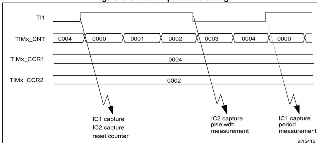
- 1. The PWM input mode can be used only with the TIMx_CH1/TIMx_CH2 signals due to the fact that only TI1FP1 and TI2FP2 are connected to the slave mode controller.
34.3.7 Forced output mode
In output mode (CCxS bits = 00 in the TIMx_CCMRx register), each output compare signal (OCxREF and then OCx) can be forced to active or inactive level directly by software, independently of any comparison between the output compare register and the counter.
To force an output compare signal (ocxref/OCx) to its active level, one just needs to write 101 in the OCxM bits in the corresponding TIMx_CCMRx register. Thus ocxref is forced high (OCxREF is always active high) and OCx get opposite value to CCxP polarity bit.
e.g.: CCxP=0 (OCx active high) => OCx is forced to high level.
ocxref signal can be forced low by writing the OCxM bits to 100 in the TIMx_CCMRx register.
Anyway, the comparison between the TIMx_CCRx shadow register and the counter is still performed and allows the flag to be set. Interrupt and DMA requests can be sent accordingly. This is described in the Output Compare Mode section.
34.3.8 Output compare mode
This function is used to control an output waveform or indicating when a period of time has elapsed.
When a match is found between the capture/compare register and the counter, the output compare function:
- • Assigns the corresponding output pin to a programmable value defined by the output compare mode (OCxM bits in the TIMx_CCMRx register) and the output polarity (CCxP bit in the TIMx_CCER register). The output pin can keep its level (OCXM=000), be set active (OCxM=001), be set inactive (OCxM=010) or can toggle (OCxM=011) on match.
- • Sets a flag in the interrupt status register (CCxIF bit in the TIMx_SR register).
- • Generates an interrupt if the corresponding interrupt mask is set (CCxIE bit in the TIMx_DIER register).
- • Sends a DMA request if the corresponding enable bit is set (CCxDE bit in the TIMx_DIER register, CCDS bit in the TIMx_CR2 register for the DMA request selection).
The TIMx_CCRx registers can be programmed with or without preload registers using the OCxPE bit in the TIMx_CCMRx register.
In output compare mode, the update event UEV has no effect on ocxref and OCx output. The timing resolution is one count of the counter. Output compare mode can also be used to output a single pulse (in One-pulse mode).
Procedure
- 1. Select the counter clock (internal, external, prescaler).
- 2. Write the desired data in the TIMx_ARR and TIMx_CCRx registers.
- 3. Set the CCxIE and/or CCxDE bits if an interrupt and/or a DMA request is to be generated.
- 4. Select the output mode. For example, one must write OCxM=011, OCxPE=0, CCxP=0 and CCxE=1 to toggle OCx output pin when CNT matches CCRx, CCRx preload is not used, OCx is enabled and active high.
- 5. Enable the counter by setting the CEN bit in the TIMx_CR1 register.
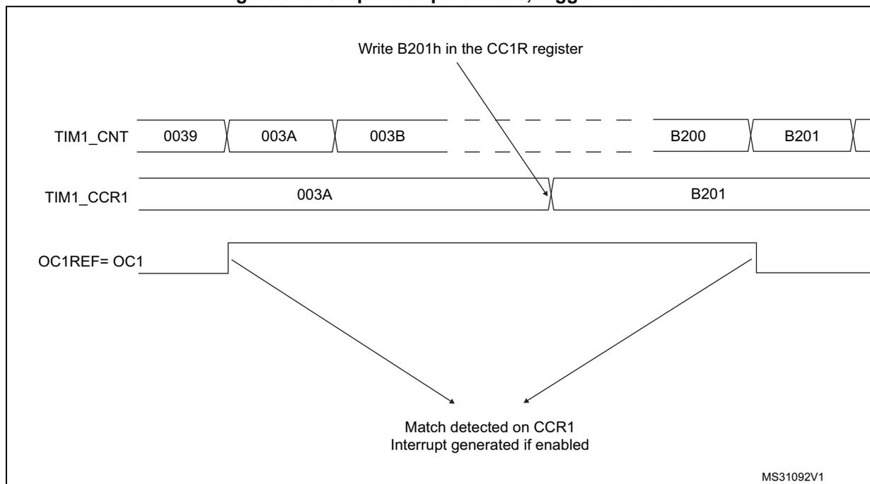
The TIMx_CCRx register can be updated at any time by software to control the output waveform, provided that the preload register is not enabled (OCxPE=0, else TIMx_CCRx shadow register is updated only at the next update event UEV). An example is given in Figure 320 .
Figure 320. Output compare mode, toggle on OC1
34.3.9 PWM mode
Pulse width modulation mode permits to generate a signal with a frequency determined by the value of the TIMx_ARR register and a duty cycle determined by the value of the TIMx_CCRx register.
The PWM mode can be selected independently on each channel (one PWM per OCx output) by writing 110 (PWM mode 1) or '111 (PWM mode 2) in the OCxM bits in the TIMx_CCMRx register. The corresponding preload register must be enabled by setting the OCxPE bit in the TIMx_CCMRx register, and eventually the auto-reload preload register (in upcounting or center-aligned modes) by setting the ARPE bit in the TIMx_CR1 register.
As the preload registers are transferred to the shadow registers only when an update event occurs, before starting the counter, all registers must be initialized by setting the UG bit in the TIMx_EGR register.
OCx polarity is software programmable using the CCxP bit in the TIMx_CCER register. It can be programmed as active high or active low. OCx output is enabled by the CCxE bit in the TIMx_CCER register. Refer to the TIMx_CCERx register description for more details.
In PWM mode (1 or 2), TIMx_CNT and TIMx_CCRx are always compared to determine whether \( TIMx\_CCRx \leq TIMx\_CNT \) or \( TIMx\_CNT \leq TIMx\_CCRx \) (depending on the direction of the counter). However, to comply with the OCREF_CLR functionality (OCREF can be cleared by an external event through the ETR signal until the next PWM period), the OCREF signal is asserted only:
- • When the result of the comparison or
- • When the output compare mode (OCxM bits in TIMx_CCMRx register) switches from the “frozen” configuration (no comparison, OCxM='000) to one of the PWM modes (OCxM='110 or '111).
This forces the PWM by software while the timer is running.
The timer is able to generate PWM in edge-aligned mode or center-aligned mode depending on the CMS bits in the \( TIMx\_CR1 \) register.
PWM edge-aligned mode
Upcounting configuration
Upcounting is active when the DIR bit in the \( TIMx\_CR1 \) register is low. Refer to Upcounting mode on page 1181 .
In the following example, we consider PWM mode 1. The reference PWM signal OCxREF is high as long as \( TIMx\_CNT < TIMx\_CCRx \) else it becomes low. If the compare value in \( TIMx\_CCRx \) is greater than the auto-reload value (in \( TIMx\_ARR \) ) then OCxREF is held at '1'. If the compare value is 0 then OCxREF is held at '0'. Figure 321 shows some edge-aligned PWM waveforms in an example where \( TIMx\_ARR=8 \) .
Figure 321. Edge-aligned PWM waveforms (ARR=8)
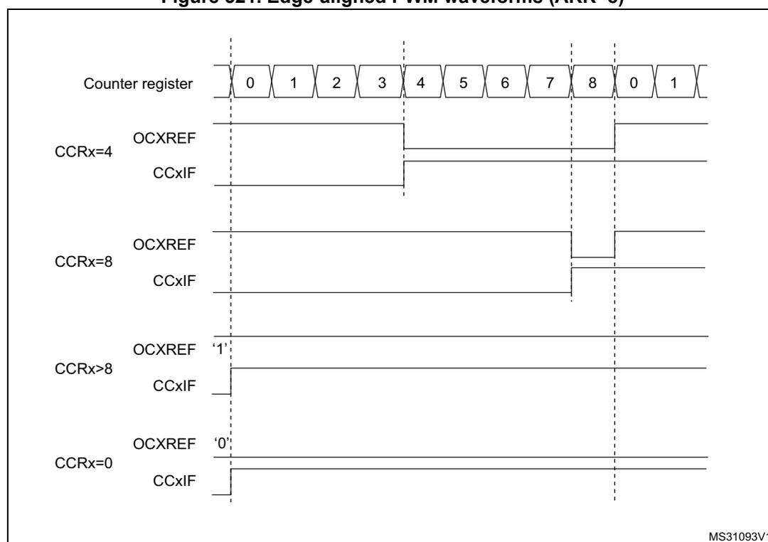
The figure is a timing diagram illustrating edge-aligned PWM waveforms for a timer with an auto-reload register (ARR) value of 8. The top row shows the Counter register ( \( TIMx\_CNT \) ) values: 0, 1, 2, 3, 4, 5, 6, 7, 8, 0, 1. Below this, four sets of waveforms are shown for different compare register (CCR) values:
- CCRx=4: The OCxREF signal is high from counter value 0 to 4, and low from 4 to 8. The CCxIF flag pulses when the counter reaches 4.
- CCRx=8: The OCxREF signal is high from counter value 0 to 8, and low at 0. The CCxIF flag pulses when the counter reaches 8.
- CCRx>8: The OCxREF signal is always high ('1'). The CCxIF flag pulses at the counter overflow (transition from 8 to 0).
- CCRx=0: The OCxREF signal is always low ('0'). The CCxIF flag pulses at the counter overflow (transition from 8 to 0).
Vertical dashed lines indicate the counter values 0, 4, 8, and 0. The diagram is labeled MS31093V1 in the bottom right corner.
Downcounting configuration
Downcounting is active when DIR bit in \( TIMx\_CR1 \) register is high. Refer to Downcounting mode on page 1184 .
In PWM mode 1, the reference signal ocxref is low as long as \( TIMx\_CNT > TIMx\_CCRx \) else it becomes high. If the compare value in \( TIMx\_CCRx \) is greater than the auto-reload value in \( TIMx\_ARR \) , then ocxref is held at 100%. PWM is not possible in this mode.
PWM center-aligned mode
Center-aligned mode is active when the CMS bits in \( TIMx\_CR1 \) register are different from '00 (all the remaining configurations having the same effect on the ocxref/OCx signals). The
compare flag is set when the counter counts up, when it counts down or both when it counts up and down depending on the CMS bits configuration. The direction bit (DIR) in the TIMx_CR1 register is updated by hardware and must not be changed by software. Refer to Center-aligned mode (up/down counting) on page 1187 .
Figure 322 shows some center-aligned PWM waveforms in an example where:
- • TIMx_ARR =8,
- • PWM mode is the PWM mode 1,
- • The flag is set when the counter counts down corresponding to the center-aligned mode 1 selected for CMS=01 in TIMx_CR1 register.
Figure 322. Center-aligned PWM waveforms (ARR=8)
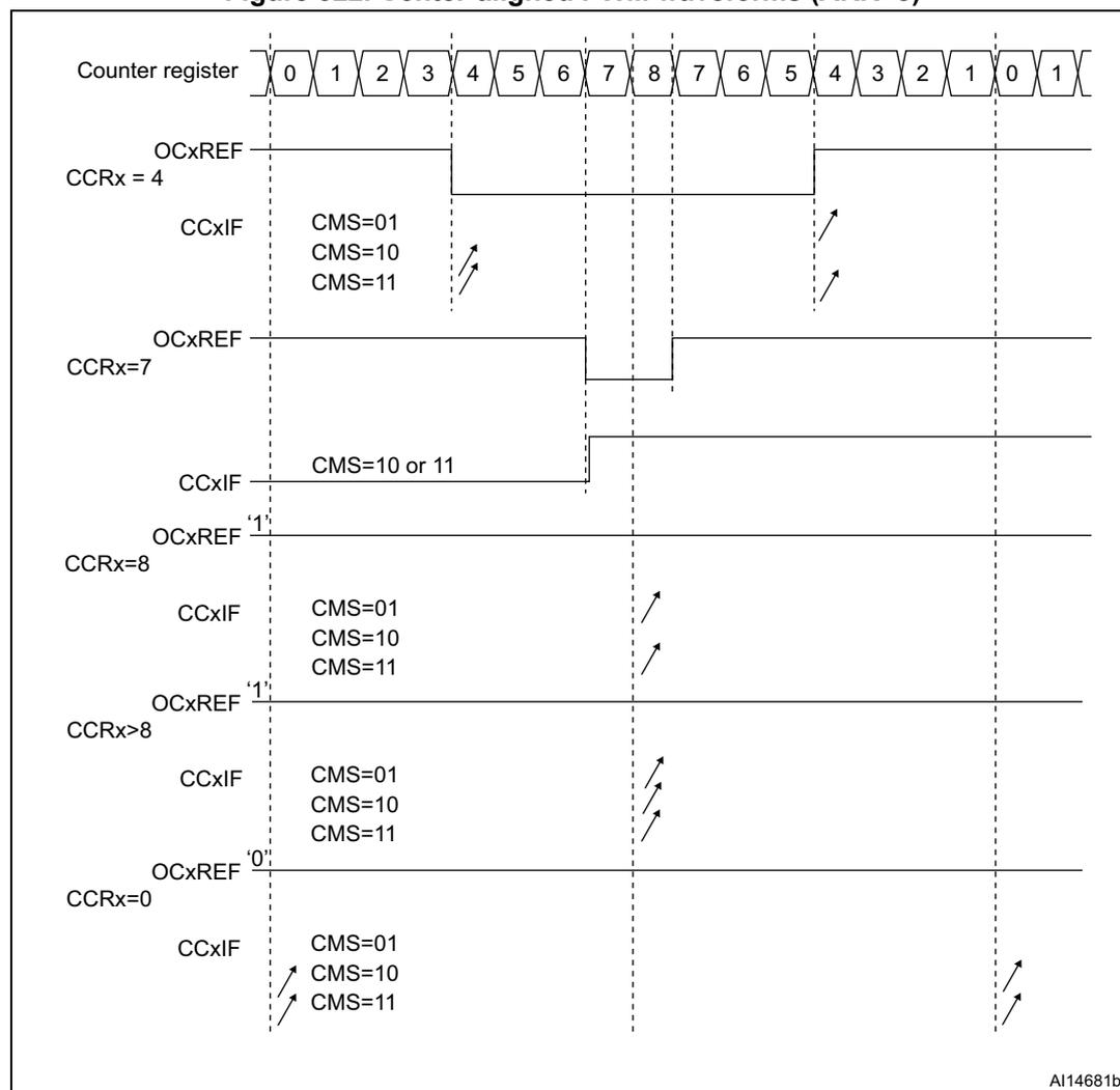
The diagram illustrates the behavior of the OCxREF signal and CCxIF flag for various CCRx values relative to a counter counting from 0 to 8 and back to 0.
- Counter register: 0 1 2 3 4 5 6 7 8 7 6 5 4 3 2 1 0 1
- CCRx = 4: OCxREF transitions at counter value 4. CCxIF triggers on downcount for CMS=01, upcount for CMS=10, and both for CMS=11.
- CCRx = 7: OCxREF transitions at counter value 7. CCxIF triggers for CMS=10 or 11 at the peak.
- CCRx = 8: OCxREF is constant '1'. CCxIF triggers at counter value 8 for various CMS settings.
- CCRx > 8: OCxREF is constant '1'. CCxIF triggers at counter value 8.
- CCRx = 0: OCxREF is constant '0'. CCxIF triggers at counter value 0.
AI14681b
Hints on using center-aligned mode:
- • When starting in center-aligned mode, the current up-down configuration is used. It means that the counter counts up or down depending on the value written in the DIR bit
in the TIMx_CR1 register. Moreover, the DIR and CMS bits must not be changed at the same time by the software.
- • Writing to the counter while running in center-aligned mode is not recommended as it can lead to unexpected results. In particular:
- – The direction is not updated if a value greater than the auto-reload value is written in the counter (TIMx_CNT > TIMx_ARR). For example, if the counter was counting up, it continues to count up.
- – The direction is updated if 0 or the TIMx_ARR value is written in the counter but no Update Event UEV is generated.
- • The safest way to use center-aligned mode is to generate an update by software (setting the UG bit in the TIMx_EGR register) just before starting the counter and not to write the counter while it is running.
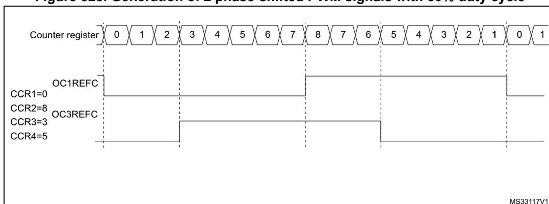
34.3.10 Asymmetric PWM mode
Asymmetric mode allows two center-aligned PWM signals to be generated with a programmable phase shift. While the frequency is determined by the value of the TIMx_ARR register, the duty cycle and the phase-shift are determined by a pair of TIMx_CCRx registers. One register controls the PWM during up-counting, the second during down counting, so that PWM is adjusted every half PWM cycle:
- • OC1REFC (or OC2REFC) is controlled by TIMx_CCR1 and TIMx_CCR2
- • OC3REFC (or OC4REFC) is controlled by TIMx_CCR3 and TIMx_CCR4
Asymmetric PWM mode can be selected independently on two channels (one OCx output per pair of CCR registers) by writing '1110' (Asymmetric PWM mode 1) or '1111' (Asymmetric PWM mode 2) in the OCxM bits in the TIMx_CCMRx register.
Note: The OCxM[3:0] bit field is split into two parts for compatibility reasons, the most significant bit is not contiguous with the 3 least significant ones.
When a given channel is used as asymmetric PWM channel, its secondary channel can also be used. For instance, if an OC1REFC signal is generated on channel 1 (Asymmetric PWM mode 1), it is possible to output either the OC2REF signal on channel 2, or an OC2REFC signal resulting from asymmetric PWM mode 2.
Figure 323 shows an example of signals that can be generated using Asymmetric PWM mode (channels 1 to 4 are configured in Asymmetric PWM mode 1).
Figure 323. Generation of 2 phase-shifted PWM signals with 50% duty cycle
34.3.11 Combined PWM mode
Combined PWM mode allows two edge or center-aligned PWM signals to be generated with programmable delay and phase shift between respective pulses. While the frequency is determined by the value of the TIMx_ARR register, the duty cycle and delay are determined by the two TIMx_CCRx registers. The resulting signals, OCxREFC, are made of an OR or AND logical combination of two reference PWMs:
- – OC1REFC (or OC2REFC) is controlled by TIMx_CCR1 and TIMx_CCR2
- – OC3REFC (or OC4REFC) is controlled by TIMx_CCR3 and TIMx_CCR4
Combined PWM mode can be selected independently on two channels (one OCx output per pair of CCR registers) by writing '1100' (Combined PWM mode 1) or '1101' (Combined PWM mode 2) in the OCxM bits in the TIMx_CCMRx register.
When a given channel is used as combined PWM channel, its secondary channel must be configured in the opposite PWM mode (for instance, one in Combined PWM mode 1 and the other in Combined PWM mode 2).
Note: The OCxM[3:0] bit field is split into two parts for compatibility reasons, the most significant bit is not contiguous with the 3 least significant ones.
Figure 324 shows an example of signals that can be generated using Asymmetric PWM mode, obtained with the following configuration:
- • Channel 1 is configured in Combined PWM mode 2,
- • Channel 2 is configured in PWM mode 1,
- • Channel 3 is configured in Combined PWM mode 2,
- • Channel 4 is configured in PWM mode 1
Figure 324. Combined PWM mode on channels 1 and 3
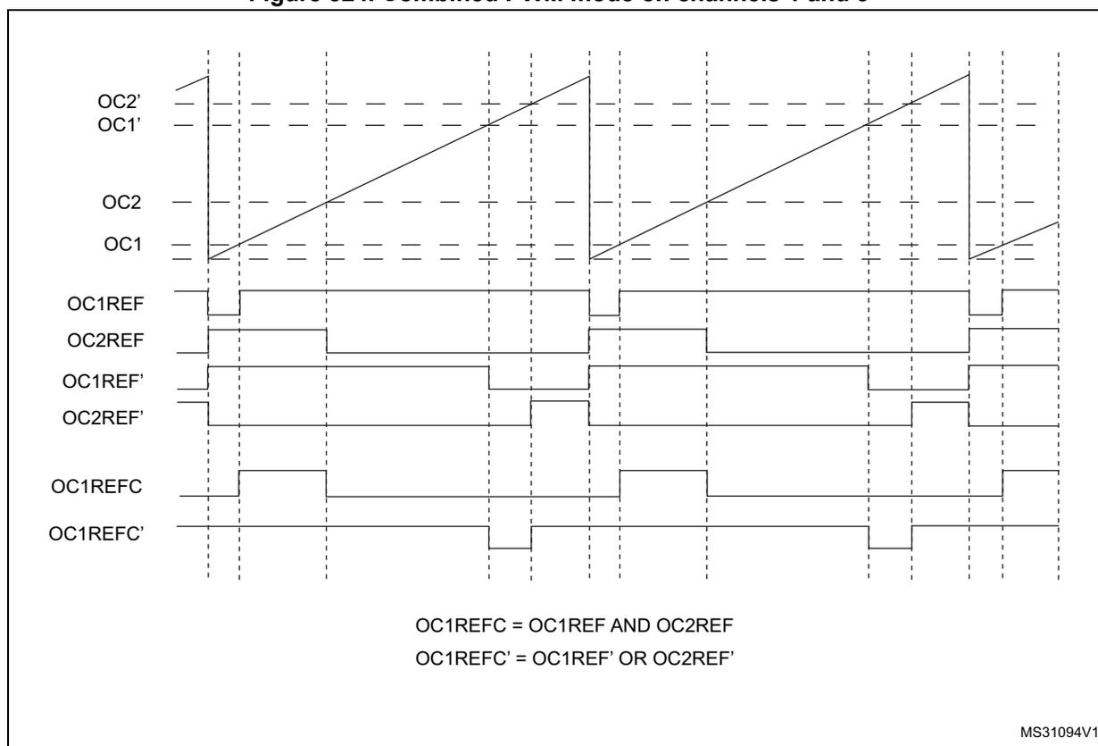
OC1REFC = OC1REF AND OC2REF
OC1REFC' = OC1REF' OR OC2REF'
MS31094V1
34.3.12 Clearing the OCxREF signal on an external event
The OCxREF signal of a given channel can be cleared when a high level is applied on the ocref_clr_int input (OCxCE enable bit in the corresponding TIMx_CCMRx register set to 1). OCxREF remains low until the next transition to the active state, on the following PWM cycle. This function can only be used in Output compare and PWM modes. It does not work in Forced mode.
The ocref_clr_int is connected to the ETRF signal (ETR after filtering).
The OCxREF signal for a given channel can be reset by applying a high level on the ETRF input (OCxCE enable bit set to 1 in the corresponding TIMx_CCMRx register). OCxREF remains low until the next transition to the active state, on the following PWM cycle.
This function can be used only in the output compare and PWM modes. It does not work in forced mode.
For example, the OCxREF signal can be connected to the output of a comparator to be used for current handling. In this case, ETR must be configured as follows:
- 1. The external trigger prescaler should be kept off: bits ETPS[1:0] in the TIMx_SMCR register are cleared to 00.
- 2. The external clock mode 2 must be disabled: bit ECE in the TIM1_SMCR register is cleared to 0.
- 3. The external trigger polarity (ETP) and the external trigger filter (ETF) can be configured according to the application's needs.
Figure 325 shows the behavior of the OCxREF signal when the ETRF input becomes high, for both values of the OCxCE enable bit. In this example, the timer TIMx is programmed in PWM mode.
Figure 325. Clearing TIMx OCxREF
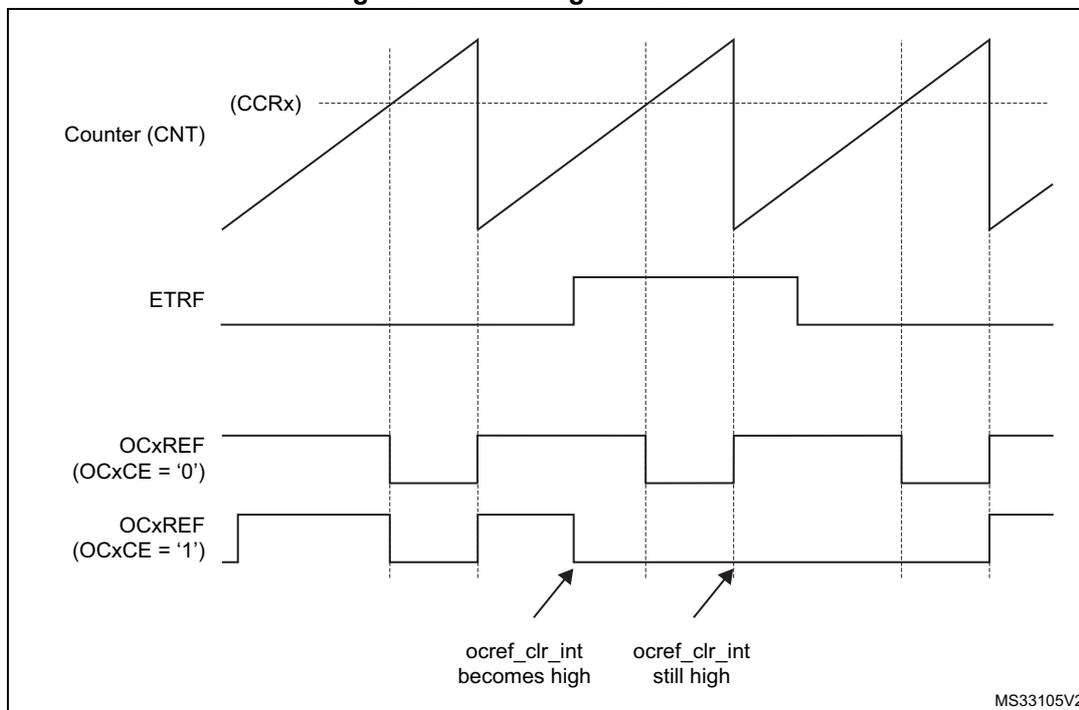
The figure is a timing diagram illustrating the behavior of the OCxREF signal in a timer (TIMx) programmed in PWM mode. It shows four waveforms over time:
- Counter (CNT) (CCRx): A sawtooth waveform representing the counter value. It increases linearly and then resets to zero at each overflow.
- ETRF: An external trigger input signal. It is shown as a rectangular pulse that goes high and then low.
- OCxREF (OCxCE = '0'): The output compare reference signal when the OCxCE bit is set to '0'. This signal is active-low. It goes high when the ETRF signal goes high and returns to low when the ETRF signal goes low.
- OCxREF (OCxCE = '1'): The output compare reference signal when the OCxCE bit is set to '1'. This signal is active-high. It goes high when the ETRF signal goes high and remains high until the next counter overflow. Two arrows point to this signal: one at the rising edge labeled "ocref_clr_int becomes high" and another at the falling edge labeled "ocref_clr_int still high".
The diagram is labeled MS33105V2.
Note: In case of a PWM with a 100% duty cycle (if \( CCRx > ARR \) ), OCxREF is enabled again at the next counter overflow.
34.3.13 One-pulse mode
One-pulse mode (OPM) is a particular case of the previous modes. It allows the counter to be started in response to a stimulus and to generate a pulse with a programmable length after a programmable delay.
Starting the counter can be controlled through the slave mode controller. Generating the waveform can be done in output compare mode or PWM mode. One-pulse mode is selected by setting the OPM bit in the TIMx_CR1 register. This makes the counter stop automatically at the next update event UEV.
A pulse can be correctly generated only if the compare value is different from the counter initial value. Before starting (when the timer is waiting for the trigger), the configuration must be:
- • \( CNT < CCRx \leq ARR \) (in particular, \( 0 < CCRx \) ),
Figure 326. Example of one-pulse mode.
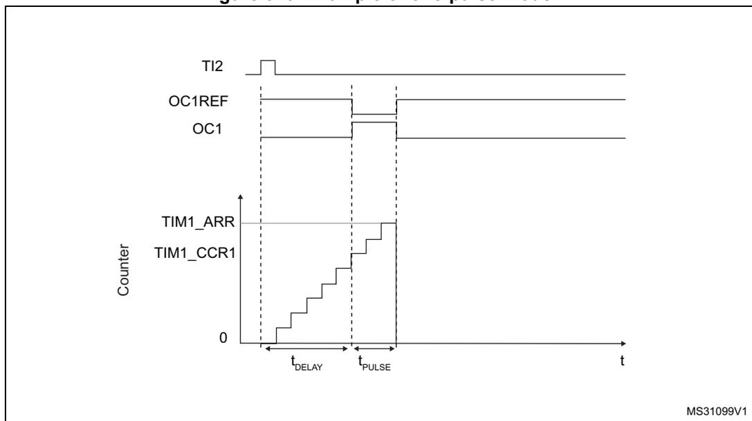
For example one may want to generate a positive pulse on OC1 with a length of \( t_{PULSE} \) and after a delay of \( t_{DELAY} \) as soon as a positive edge is detected on the TI2 input pin.
Let's use TI2FP2 as trigger 1:
- 1. Map TI2FP2 on TI2 by writing CC2S=01 in the TIMx_CCMR1 register.
- 2. TI2FP2 must detect a rising edge, write CC2P=0 and CC2NP='0' in the TIMx_CCER register.
- 3. Configure TI2FP2 as trigger for the slave mode controller (TRGI) by writing TS=110 in the TIMx_SMCR register.
- 4. TI2FP2 is used to start the counter by writing SMS to '110 in the TIMx_SMCR register (trigger mode).
The OPM waveform is defined by writing the compare registers (taking into account the clock frequency and the counter prescaler).
- • The \( t_{\text{DELAY}} \) is defined by the value written in the TIMx_CCR1 register.
- • The \( t_{\text{PULSE}} \) is defined by the difference between the auto-reload value and the compare value (TIMx_ARR - TIMx_CCR1).
- • Let's say one wants to build a waveform with a transition from '0' to '1' when a compare match occurs and a transition from '1' to '0' when the counter reaches the auto-reload value. To do this PWM mode 2 must be enabled by writing OC1M=111 in the TIMx_CCMR1 register. Optionally the preload registers can be enabled by writing OC1PE=1 in the TIMx_CCMR1 register and ARPE in the TIMx_CR1 register. In this case one has to write the compare value in the TIMx_CCR1 register, the auto-reload value in the TIMx_ARR register, generate an update by setting the UG bit and wait for external trigger event on TI2. CC1P is written to '0' in this example.
In our example, the DIR and CMS bits in the TIMx_CR1 register should be low.
Since only 1 pulse (Single mode) is needed, a 1 must be written in the OPM bit in the TIMx_CR1 register to stop the counter at the next update event (when the counter rolls over from the auto-reload value back to 0). When OPM bit in the TIMx_CR1 register is set to '0', so the Repetitive Mode is selected.
Particular case: OCx fast enable:
In One-pulse mode, the edge detection on TIx input set the CEN bit which enables the counter. Then the comparison between the counter and the compare value makes the output toggle. But several clock cycles are needed for these operations and it limits the minimum delay \( t_{\text{DELAY}} \) min we can get.
If one wants to output a waveform with the minimum delay, the OCxFE bit can be set in the TIMx_CCMRx register. Then OCxRef (and OCx) is forced in response to the stimulus, without taking in account the comparison. Its new level is the same as if a compare match had occurred. OCxFE acts only if the channel is configured in PWM1 or PWM2 mode.
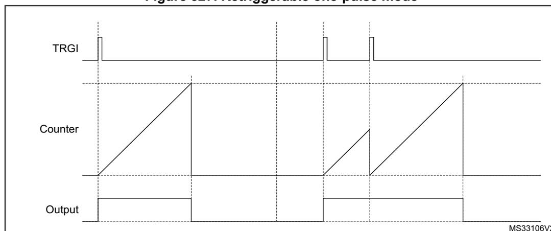
34.3.14 Retriggerable one pulse mode
This mode allows the counter to be started in response to a stimulus and to generate a pulse with a programmable length, but with the following differences with Non-retriggerable one pulse mode described in Section 34.3.13 :
- • The pulse starts as soon as the trigger occurs (no programmable delay)
- • The pulse is extended if a new trigger occurs before the previous one is completed
The timer must be in Slave mode, with the bits SMS[3:0] = '1000' (Combined Reset + trigger mode) in the TIMx_SMCR register, and the OCxM[3:0] bits set to '1000' or '1001' for Retriggerable OPM mode 1 or 2.
If the timer is configured in Up-counting mode, the corresponding CCRx must be set to 0 (the ARR register sets the pulse length). If the timer is configured in Down-counting mode CCRx must be above or equal to ARR.
Note: In retriggerable one pulse mode, the CCxIF flag is not significant.
The OCxM[3:0] and SMS[3:0] bit fields are split into two parts for compatibility reasons, the most significant bit is not contiguous with the 3 least significant ones.
This mode must not be used with center-aligned PWM modes. It is mandatory to have CMS[1:0] = 00 in TIMx_CR1.
Figure 327. Retriggerable one-pulse mode
34.3.15 Encoder interface mode
To select Encoder Interface mode write SMS='001 in the TIMx_SMCR register if the counter is counting on TI2 edges only, SMS=010 if it is counting on TI1 edges only and SMS=011 if it is counting on both TI1 and TI2 edges.
Select the TI1 and TI2 polarity by programming the CC1P and CC2P bits in the TIMx_CCER register. CC1NP and CC2NP must be kept cleared. When needed, the input filter can be programmed as well. CC1NP and CC2NP must be kept low.
The two inputs TI1 and TI2 are used to interface to an incremental encoder. Refer to Table 284 . The counter is clocked by each valid transition on TI1FP1 or TI2FP2 (TI1 and TI2 after input filter and polarity selection, TI1FP1=TI1 if not filtered and not inverted, TI2FP2=TI2 if not filtered and not inverted) assuming that it is enabled (CEN bit in TIMx_CR1 register written to '1'). The sequence of transitions of the two inputs is evaluated and generates count pulses as well as the direction signal. Depending on the sequence the counter counts up or down, the DIR bit in the TIMx_CR1 register is modified by hardware accordingly. The DIR bit is calculated at each transition on any input (TI1 or TI2), whatever the counter is counting on TI1 only, TI2 only or both TI1 and TI2.
Encoder interface mode acts simply as an external clock with direction selection. This means that the counter just counts continuously between 0 and the auto-reload value in the TIMx_ARR register (0 to ARR or ARR down to 0 depending on the direction). So the TIMx_ARR must be configured before starting. In the same way, the capture, compare, prescaler, trigger output features continue to work as normal.
In this mode, the counter is modified automatically following the speed and the direction of the quadrature encoder and its content, therefore, always represents the encoder's position. The count direction correspond to the rotation direction of the connected sensor. The table summarizes the possible combinations, assuming TI1 and TI2 do not switch at the same time.
Table 284. Counting direction versus encoder signals
| Active edge | Level on opposite signal (TI1FP1 for TI2, TI2FP2 for TI1) | TI1FP1 signal | TI2FP2 signal | ||
|---|---|---|---|---|---|
| Rising | Falling | Rising | Falling | ||
| Counting on TI1 only | High | Down | Up | No Count | No Count |
| Low | Up | Down | No Count | No Count | |
| Counting on TI2 only | High | No Count | No Count | Up | Down |
| Low | No Count | No Count | Down | Up | |
| Counting on TI1 and TI2 | High | Down | Up | Up | Down |
| Low | Up | Down | Down | Up | |
An external incremental encoder can be connected directly to the MCU without external interface logic. However, comparators are normally used to convert the encoder's differential outputs to digital signals. This greatly increases noise immunity. The third encoder output which indicate the mechanical zero position, may be connected to an external interrupt input and trigger a counter reset.
Figure 328 gives an example of counter operation, showing count signal generation and direction control. It also shows how input jitter is compensated where both edges are selected. This might occur if the sensor is positioned near to one of the switching points. For this example we assume that the configuration is the following:
- • CC1S= 01 (TIMx_CCMR1 register, TI1FP1 mapped on TI1)
- • CC2S= 01 (TIMx_CCMR1 register, TI2FP2 mapped on TI2)
- • CC1P and CC1NP = '0' (TIMx_CCER register, TI1FP1 noninverted, TI1FP1=TI1)
- • CC2P and CC2NP = '0' (TIMx_CCER register, TI2FP2 noninverted, TI2FP2=TI2)
- • SMS= 011 (TIMx_SMCR register, both inputs are active on both rising and falling edges)
- • CEN= 1 (TIMx_CR1 register, Counter is enabled)
Figure 328. Example of counter operation in encoder interface mode
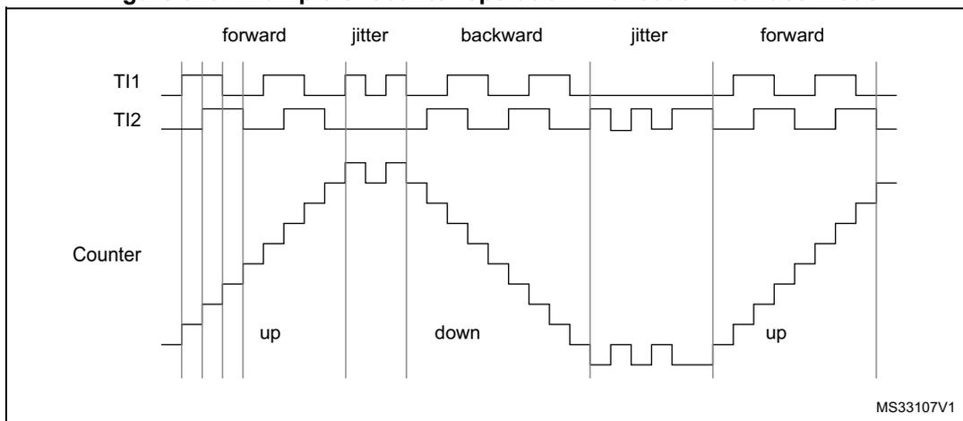
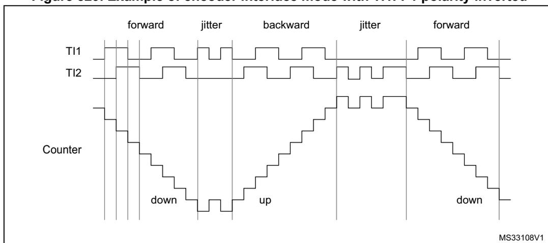
Figure 329 gives an example of counter behavior when TI1FP1 polarity is inverted (same configuration as above except CC1P=1).
Figure 329. Example of encoder interface mode with TI1FP1 polarity inverted
The timer, when configured in Encoder Interface mode provides information on the sensor's current position. Dynamic information can be obtained (speed, acceleration, deceleration) by measuring the period between two encoder events using a second timer configured in capture mode. The output of the encoder which indicates the mechanical zero can be used for this purpose. Depending on the time between two events, the counter can also be read at regular times. This can be done by latching the counter value into a third input capture register if available (then the capture signal must be periodic and can be generated by another timer). When available, it is also possible to read its value through a DMA request generated by a Real-Time clock.
34.3.16 UIF bit remapping
The IUFREMAP bit in the TIMx_CR1 register forces a continuous copy of the update interrupt flag (UIF) into bit 31 of the timer counter register's bit 31 (TIMxCNT[31]). This permits to atomically read both the counter value and a potential roll-over condition signaled by the UIFCPY flag. It eases the calculation of angular speed by avoiding race conditions caused, for instance, by a processing shared between a background task (counter reading) and an interrupt (update interrupt).
There is no latency between the UIF and UIFCPY flag assertions.
In 32-bit timer implementations, when the IUFREMAP bit is set, bit 31 of the counter is overwritten by the UIFCPY flag upon read access (the counter's most significant bit is only accessible in write mode).
34.3.17 Timer input XOR function
The TI1S bit in the TIM1xx_CR2 register, allows the input filter of channel 1 to be connected to the output of a XOR gate, combining the three input pins TIMx_CH1 to TIMx_CH3.
The XOR output can be used with all the timer input functions such as trigger or input capture.
An example of this feature used to interface Hall sensors is given in Section 33.3.25: Interfacing with Hall sensors on page 1123 .
34.3.18 Timers and external trigger synchronization
The TIMx Timers can be synchronized with an external trigger in several modes: Reset mode, Gated mode and Trigger mode.
Slave mode: Reset mode
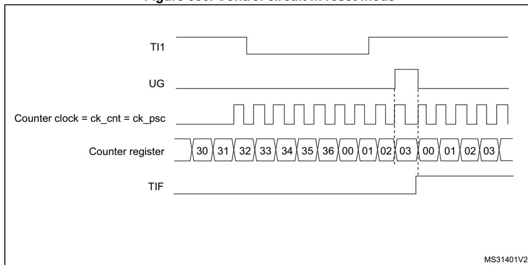
The counter and its prescaler can be reinitialized in response to an event on a trigger input. Moreover, if the URS bit from the TIMx_CR1 register is low, an update event UEV is generated. Then all the preloaded registers (TIMx_ARR, TIMx_CCRx) are updated.
In the following example, the upcounter is cleared in response to a rising edge on TI1 input:
- 1. Configure the channel 1 to detect rising edges on TI1. Configure the input filter duration (in this example, we do not need any filter, so we keep IC1F=0000). The capture prescaler is not used for triggering, so it does not need to be configured. The CC1S bits select the input capture source only, CC1S = 01 in the TIMx_CCMR1 register. Write CC1P=0 and CC1NP=0 in TIMx_CCER register to validate the polarity (and detect rising edges only).
- 2. Configure the timer in reset mode by writing SMS=100 in TIMx_SMCR register. Select TI1 as the input source by writing TS=101 in TIMx_SMCR register.
- 3. Start the counter by writing CEN=1 in the TIMx_CR1 register.
The counter starts counting on the internal clock, then behaves normally until TI1 rising edge. When TI1 rises, the counter is cleared and restarts from 0. In the meantime, the trigger flag is set (TIF bit in the TIMx_SR register) and an interrupt request, or a DMA request can be sent if enabled (depending on the TIE and TDE bits in TIMx_DIER register).
The following figure shows this behavior when the auto-reload register TIMx_ARR=0x36. The delay between the rising edge on TI1 and the actual reset of the counter is due to the resynchronization circuit on TI1 input.
Figure 330. Control circuit in reset mode
Slave mode: Gated mode
The counter can be enabled depending on the level of a selected input.
In the following example, the upcounter counts only when TI1 input is low:
- 1. Configure the channel 1 to detect low levels on TI1. Configure the input filter duration (in this example, we do not need any filter, so we keep IC1F=0000). The capture prescaler is not used for triggering, so it does not need to be configured. The CC1S bits select the input capture source only, CC1S=01 in TIMx_CCMR1 register. Write CC1P=1 and CC1NP=0 in TIMx_CCER register to validate the polarity (and detect low level only).
- 2. Configure the timer in gated mode by writing SMS=101 in TIMx_SMCR register. Select TI1 as the input source by writing TS=101 in TIMx_SMCR register.
- 3. Enable the counter by writing CEN=1 in the TIMx_CR1 register (in gated mode, the counter doesn't start if CEN=0, whatever is the trigger input level).
The counter starts counting on the internal clock as long as TI1 is low and stops as soon as TI1 becomes high. The TIF flag in the TIMx_SR register is set both when the counter starts or stops.
The delay between the rising edge on TI1 and the actual stop of the counter is due to the resynchronization circuit on TI1 input.
Figure 331. Control circuit in gated mode
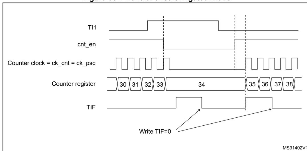
- 1. The configuration "CCxP=CCxNP=1" (detection of both rising and falling edges) does not have any effect in gated mode because gated mode acts on a level and not on an edge.
Note: The configuration "CCxP=CCxNP=1" (detection of both rising and falling edges) does not have any effect in gated mode because gated mode acts on a level and not on an edge.
Slave mode: Trigger mode
The counter can start in response to an event on a selected input.
In the following example, the upcounter starts in response to a rising edge on TI2 input:
- 1. Configure the channel 2 to detect rising edges on TI2. Configure the input filter duration (in this example, we do not need any filter, so we keep IC2F=0000). The capture prescaler is not used for triggering, so it does not need to be configured. CC2S bits are selecting the input capture source only, CC2S=01 in TIMx_CCMR1 register. Write
CC2P=1 and CC2NP=0 in TIMx_CCER register to validate the polarity (and detect low level only).
- 2. Configure the timer in trigger mode by writing SMS=110 in TIMx_SMCR register. Select TI2 as the input source by writing TS=110 in TIMx_SMCR register.
When a rising edge occurs on TI2, the counter starts counting on the internal clock and the TIF flag is set.
The delay between the rising edge on TI2 and the actual start of the counter is due to the resynchronization circuit on TI2 input.
Figure 332. Control circuit in trigger mode
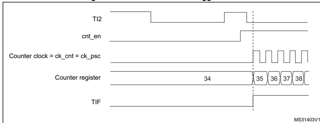
Timing diagram showing the control circuit in trigger mode. The diagram illustrates the relationship between the TI2 input, counter enable (cnt_en), counter clock (ck_cnt = ck_psc), counter register value, and the TIF flag. The TI2 input shows a rising edge. The counter enable (cnt_en) is generated by the rising edge of TI2. The counter clock (ck_cnt = ck_psc) is a periodic square wave. The counter register value starts at 34 and increments to 35, 36, 37, and 38 upon each rising edge of the clock. The TIF flag is set by the rising edge of TI2 and returns low after a short duration. A vertical dashed line marks the rising edge of TI2. The identifier MS31403V1 is in the bottom right corner.
Slave mode: Combined reset + trigger mode
In this case, a rising edge of the selected trigger input (TRGI) reinitializes the counter, generates an update of the registers, and starts the counter.
This mode is used for one-pulse mode.
Slave mode: External Clock mode 2 + trigger mode
The external clock mode 2 can be used in addition to another slave mode (except external clock mode 1 and encoder mode). In this case, the ETR signal is used as external clock input, and another input can be selected as trigger input when operating in reset mode, gated mode or trigger mode. It is recommended not to select ETR as TRGI through the TS bits of TIMx_SMCR register.
In the following example, the upcounter is incremented at each rising edge of the ETR signal as soon as a rising edge of TI1 occurs:
- Configure the external trigger input circuit by programming the TIMx_SMCR register as follows:
- – ETF = 0000: no filter
- – ETPS=00: prescaler disabled
- – ETP=0: detection of rising edges on ETR and ECE=1 to enable the external clock mode 2.
- Configure the channel 1 as follows, to detect rising edges on TI1:
- – IC1F=0000: no filter.
- – The capture prescaler is not used for triggering and does not need to be configured.
- – CC1S=01 in TIMx_CCMR1 register to select only the input capture source
- – CC1P=0 and CC1NP=0 in TIMx_CCER register to validate the polarity (and detect rising edge only).
- Configure the timer in trigger mode by writing SMS=110 in TIMx_SMCR register. Select TI1 as the input source by writing TS=101 in TIMx_SMCR register.
A rising edge on TI1 enables the counter and sets the TIF flag. The counter then counts on ETR rising edges.
The delay between the rising edge of the ETR signal and the actual reset of the counter is due to the resynchronization circuit on ETRP input.
Figure 333. Control circuit in external clock mode 2 + trigger mode
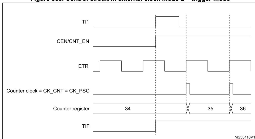
The timing diagram illustrates the control circuit in external clock mode 2 + trigger mode. It shows the following signals over time:
- TI1 : A digital signal that goes high to enable the counter and set the TIF flag.
- CEN/CNT_EN : A signal that goes high when the counter is enabled by a rising edge on TI1.
- ETR : An external trigger signal with rising edges that cause the counter to increment.
- Counter clock = CK_CNT = CK_PSC : The clock signal for the counter, which is derived from the ETR signal.
- Counter register : A register that counts the number of ETR rising edges. The values shown are 34, 35, and 36.
- TIF : A flag that is set when a rising edge is detected on the TI1 input.
34.3.19 Timer synchronization
The TIMx timers are linked together internally for timer synchronization or chaining. When one Timer is configured in Master Mode, it can reset, start, stop or clock the counter of another Timer configured in Slave Mode.
Figure 334: Master/Slave timer example and Figure 335: Master/slave connection example with 1 channel only timers present an overview of the trigger selection and the master mode selection blocks.
Figure 334. Master/Slave timer example
The diagram illustrates a master/slave timer configuration. On the left, TIM3 is shown as the master timer. It consists of a Clock input, a Prescaler, a Counter, and a Master mode control (MMS) block. The MMS block has a UEV input and a TRGO1 output. The TRGO1 output is connected to the ITR2 input of TIM2 on the right. TIM2 is shown as the slave timer. It consists of an Input trigger selection block (TS), a Slave mode control (SMS) block, a CK_PSC input, a Prescaler, and a Counter. The ITR2 input of TIM2 is connected to the TRGO1 output of TIM3.
Figure 335. Master/slave connection example with 1 channel only timers
The diagram illustrates a master/slave timer configuration using 1-channel timers. On the left, TIM_mstr (master timer) is shown. It consists of a Clock input, a Prescaler, a Counter, a Compare 1 block, and an Output control block. The Output control block has a tim_oc1 output and a TIM_CH1 input. The tim_oc1 output is connected to the tim_itr input of TIM_slv on the right. TIM_slv (slave timer) consists of an Input trigger selection block (TS), a Slave mode control (SMS) block, a CK_PSC input, a Prescaler, and a Counter. The tim_itr input of TIM_slv is connected to the tim_oc1 output of TIM_mstr.
Note: The timers with one channel only (see Figure 335) do not feature a master mode. However, the OC1 output signal can be used to trigger some other timers (including timers described in other sections of this document). Check the “TIMx internal trigger connection” table of any TIMx_SMCR register on the device to identify which timers can be targeted as slave. The OC1 signal pulse width must be programmed to be at least 2 clock cycles of the destination timer, to make sure the slave timer detects the trigger. For instance, if the destination's timer CK_INT clock is 4 times slower than the source timer, the OC1 pulse width must be 8 clock cycles.
Using one timer as prescaler for another timer
For example, TIM3 can be configured to act as a prescaler for TIM2. Refer to Figure 334. To do this:
- 1. Configure TIM3 in master mode so that it outputs a periodic trigger signal on each update event UEV. If MMS=010 is written in the TIM3_CR2 register, a rising edge is output on TRGO each time an update event is generated.
- 2. To connect the TRGO output of TIM3 to TIM2, TIM2 must be configured in slave mode using ITR2 as internal trigger. This is selected through the TS bits in the TIM2_SMCR register (writing TS=010).
- 3. Then the slave mode controller must be put in external clock mode 1 (write SMS=111 in the TIM2_SMCR register). This causes TIM2 to be clocked by the rising edge of the periodic TIM3 trigger signal (which correspond to the TIM3 counter overflow).
- 4. Finally both timers must be enabled by setting their respective CEN bits (TIMx_CR1 register).
Note: If OCx is selected on TIM3 as the trigger output (MMS=1xx), its rising edge is used to clock the counter of TIM2.
Using one timer to enable another timer
In this example, we control the enable of TIM2 with the output compare 1 of Timer 3. Refer to Figure 334 for connections. TIM2 counts on the divided internal clock only when OC1REF of TIM3 is high. Both counter clock frequencies are divided by 3 by the prescaler compared to CK_INT ( \( f_{CK\_CNT} = f_{CK\_INT}/3 \) ).
- 1. Configure TIM3 master mode to send its Output Compare 1 Reference (OC1REF) signal as trigger output (MMS=100 in the TIM3_CR2 register).
- 2. Configure the TIM3 OC1REF waveform (TIM3_CCMR1 register).
- 3. Configure TIM2 to get the input trigger from TIM3 (TS=010 in the TIM2_SMCR register).
- 4. Configure TIM2 in gated mode (SMS=101 in TIM2_SMCR register).
- 5. Enable TIM2 by writing '1' in the CEN bit (TIM2_CR1 register).
- 6. Start TIM3 by writing '1' in the CEN bit (TIM3_CR1 register).
Note: The counter 2 clock is not synchronized with counter 1, this mode only affects the TIM2 counter enable signal.
Figure 336. Gating TIM2 with OC1REF of TIM3
The timing diagram shows five horizontal signal lines over time. 1. CK_INT : A continuous square wave clock signal. 2. TIM3-OC1REF : A signal that goes high when TIM3-CNT reaches FF and goes low when it reaches 00. 3. TIM3-CNT : A counter that increments from FC to FF, then overflows to 00, then 01. 4. TIM2-CNT : A counter that increments from 3045 to 3048. It only counts when TIM3-OC1REF is high. 5. TIM2-TIF : A flag that goes high when TIM2-CNT overflows (from 3048) and is cleared by software (indicated by 'Write TIF = 0').
In the example in Figure 336 , the TIM2 counter and prescaler are not initialized before being started. So they start counting from their current value. It is possible to start from a given value by resetting both timers before starting TIM3. Then any value can be written in the timer counters. The timers can easily be reset by software using the UG bit in the TIMx_EGR registers.
In the next example (refer to Figure 337 ), we synchronize TIM3 and TIM2. TIM3 is the master and starts from 0. TIM2 is the slave and starts from 0xE7. The prescaler ratio is the same for both timers. TIM2 stops when TIM3 is disabled by writing '0' to the CEN bit in the TIM3_CR1 register:
- 1. Configure TIM3 master mode to send its Output Compare 1 Reference (OC1REF) signal as trigger output (MMS=100 in the TIM3_CR2 register).
- 2. Configure the TIM3 OC1REF waveform (TIM3_CCMR1 register).
- 3. Configure TIM2 to get the input trigger from TIM3 (TS=010 in the TIM2_SMCR register).
- 4. Configure TIM2 in gated mode (SMS=101 in TIM2_SMCR register).
- 5. Reset TIM3 by writing '1' in UG bit (TIM3_EGR register).
- 6. Reset TIM2 by writing '1' in UG bit (TIM2_EGR register).
- 7. Initialize TIM2 to 0xE7 by writing '0xE7' in the TIM2_CNT register.
- 8. Enable TIM2 by writing '1' in the CEN bit (TIM2_CR1 register).
- 9. Start TIM3 by writing '1' in the CEN bit (TIM3_CR1 register).
- 10. Stop TIM3 by writing '0' in the CEN bit (TIM3_CR1 register).
Figure 337. Gating TIM2 with Enable of TIM3
The timing diagram illustrates the sequence of events for gating TIM2 with the enable of TIM3. The signals shown are:
- CK_INT : Internal clock signal, shown as a periodic square wave.
- TIM3-CEN=CNT_EN : Enable signal for TIM3. It is initially low, goes high when TIM3 is enabled, and goes low when TIM3 is disabled.
- TIM3-CNT : Counter value for TIM3. It starts at 00, counts up to 75, then overflows to 00, 01, 02.
- TIM2-CNT : Counter value for TIM2. It starts at AB, counts up to 00, then overflows to E7, E8, E9.
- TIM2-CNT_INIT : Initialization signal for TIM2. It is initially high, goes low when TIM2 is enabled, and goes high again when TIM2 is disabled.
- TIM2-write CNT : Write signal for TIM2 counter. It is initially high, goes low when TIM2 is enabled, and goes high again when TIM2 is disabled.
- TIM2-TIF : Trigger flag for TIM2. It is initially low, goes high when TIM3 is enabled, and goes low when TIM3 is disabled. An arrow points to the falling edge with the text "Write TIF = 0".
The diagram shows that TIM2 starts counting when TIM3 is enabled and stops when TIM3 is disabled. The counter values for TIM3 are 75, 00, 01, 02. The counter values for TIM2 are AB, 00, E7, E8, E9. The TIM2-TIF flag is set when TIM3 is enabled and cleared when TIM3 is disabled.
MS33120V1
Using one timer to start another timer
In this example, we set the enable of Timer 2 with the update event of Timer 3. Refer to Figure 334 for connections. Timer 2 starts counting from its current value (which can be non-zero) on the divided internal clock as soon as the update event is generated by Timer 1. When Timer 2 receives the trigger signal its CEN bit is automatically set and the counter counts until we write '0' to the CEN bit in the TIM2_CR1 register. Both counter clock frequencies are divided by 3 by the prescaler compared to CK_INT ( \( f_{CK\_CNT} = f_{CK\_INT}/3 \) ).
- 1. Configure TIM3 master mode to send its Update Event (UEV) as trigger output (MMS=010 in the TIM3_CR2 register).
- 2. Configure the TIM3 period (TIM3_ARR registers).
- 3. Configure TIM2 to get the input trigger from TIM3 (TS=010 in the TIM2_SMCR register).
- 4. Configure TIM2 in trigger mode (SMS=110 in TIM2_SMCR register).
- 5. Start TIM3 by writing '1' in the CEN bit (TIM3_CR1 register).
Figure 338. Triggering TIM2 with update of TIM3
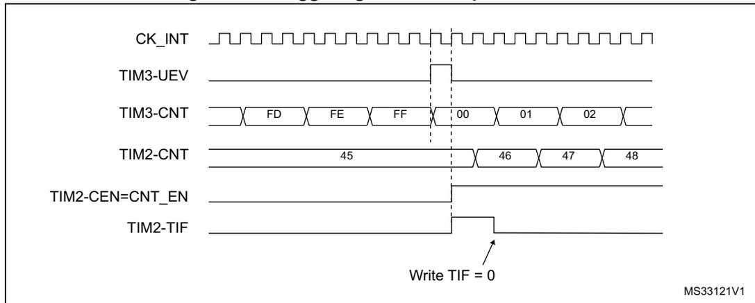
The timing diagram shows the following signals: CK_INT (clock), TIM3-UEV (Update Event), TIM3-CNT (Counter), TIM2-CNT (Counter), TIM2-CEN=CNT_EN (Counter Enable), and TIM2-TIF (Trigger Interrupt Flag). TIM3-CNT counts FD, FE, FF, then rolls over to 00, 01, 02. At the rollover from FF to 00, TIM3-UEV pulses high. This pulse causes TIM2-CEN=CNT_EN to go high. TIM2-CNT, which was at 45, then increments to 46, 47, 48 on subsequent CK_INT cycles. TIM2-TIF goes high when the trigger occurs. An arrow indicates 'Write TIF = 0' to clear the flag. Label: MS33121V1.
As in the previous example, both counters can be initialized before starting counting.
Figure 339 shows the behavior with the same configuration as in Figure 338 but in trigger mode instead of gated mode (SMS=110 in the TIM2_SMCR register).
Figure 339. Triggering TIM2 with Enable of TIM3
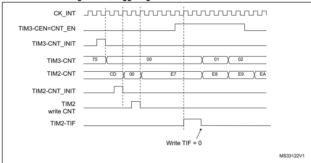
The timing diagram shows signals: CK_INT, TIM3-CEN=CNT_EN, TIM3-CNT_INIT, TIM3-CNT, TIM2-CNT, TIM2-CNT_INIT, TIM2 write CNT, and TIM2-TIF. TIM3-CNT starts at 75, then goes to 00, 01, 02. TIM3-CNT_INIT pulses high when TIM3 is enabled. TIM2-CNT starts at CD, then is forced to 00 by TIM2-CNT_INIT (triggered by TIM3 enable), and then continues counting E7, E8, E9, EA. TIM2-TIF goes high on the trigger. An arrow indicates 'Write TIF = 0'. Label: MS33122V1.
Starting 2 timers synchronously in response to an external trigger
In this example, we set the enable of TIM3 when its TI1 input rises, and the enable of TIM2 with the enable of TIM3. Refer to Figure 334 for connections. To ensure the counters are
aligned, TIM3 must be configured in Master/Slave mode (slave with respect to TI1, master with respect to TIM2):
- 1. Configure TIM3 master mode to send its Enable as trigger output (MMS=001 in the TIM3_CR2 register).
- 2. Configure TIM3 slave mode to get the input trigger from TI1 (TS=100 in the TIM3_SMCR register).
- 3. Configure TIM3 in trigger mode (SMS=110 in the TIM3_SMCR register).
- 4. Configure the TIM3 in Master/Slave mode by writing MSM=1 (TIM3_SMCR register).
- 5. Configure TIM2 to get the input trigger from TIM3 (TS=000 in the TIM2_SMCR register).
- 6. Configure TIM2 in trigger mode (SMS=110 in the TIM2_SMCR register).
When a rising edge occurs on TI1 (TIM3), both counters starts counting synchronously on the internal clock and both TIF flags are set.
Note: In this example both timers are initialized before starting (by setting their respective UG bits). Both counters starts from 0, but an offset can easily be inserted between them by writing any of the counter registers (TIMx_CNT). One can see that the master/slave mode insert a delay between CNT_EN and CK_PSC on TIM3.
Figure 340. Triggering TIM3 and TIM2 with TIM3 TI1 input
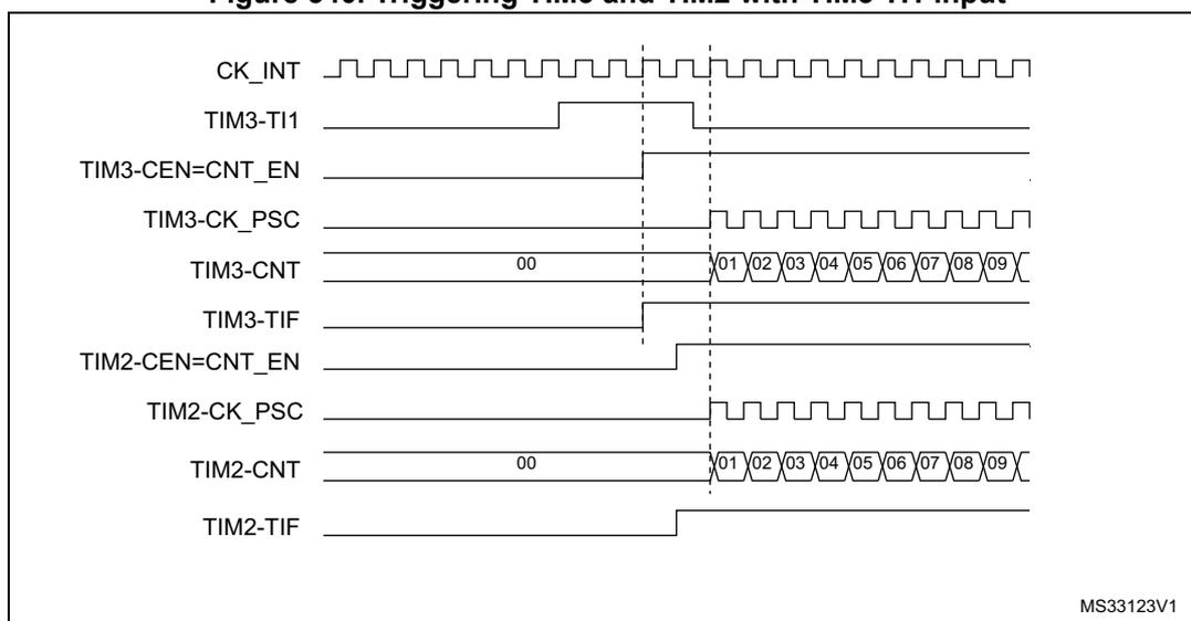
The timing diagram shows the following signals and their states over time:
- CK_INT : A continuous square wave representing the internal clock.
- TIM3-TI1 : An external input signal that goes high at a certain point in time.
- TIM3-CEN=CNT_EN : The enable signal for TIM3 counter. It goes high immediately after the rising edge of TIM3-TI1.
- TIM3-CK_PSC : The prescaled clock for TIM3. It starts after a short delay from the rising edge of TIM3-TI1.
- TIM3-CNT : The counter value for TIM3. It starts at 00 and increments (01, 02, 03, 04, 05, 06, 07, 08, 09) after the TIM3-CK_PSC starts.
- TIM3-TIF : The TIM3 interrupt flag. It goes high when the counter starts.
- TIM2-CEN=CNT_EN : The enable signal for TIM2 counter. It goes high after a delay from the TIM3-TIF signal.
- TIM2-CK_PSC : The prescaled clock for TIM2. It starts after a short delay from the rising edge of TIM2-CEN=CNT_EN.
- TIM2-CNT : The counter value for TIM2. It starts at 00 and increments (01, 02, 03, 04, 05, 06, 07, 08, 09) after the TIM2-CK_PSC starts.
- TIM2-TIF : The TIM2 interrupt flag. It goes high when the counter starts.
Vertical dashed lines indicate the sequence of events: TIM3-TI1 rising edge, TIM3-CEN=CNT_EN going high, TIM3-TIF going high, TIM2-CEN=CNT_EN going high, and TIM2-TIF going high. The counter values for TIM3 and TIM2 are shown as 00, 01, 02, 03, 04, 05, 06, 07, 08, 09, and then overflow.
MS33123V1
Note: The clock of the slave peripherals (timer, ADC, ...) receiving the TRGO or the TRGO2 signals must be enabled prior to receive events from the master timer, and the clock frequency (prescaler) must not be changed on-the-fly while triggers are received from the master timer.
34.3.20 DMA burst mode
The TIMx timers have the capability to generate multiple DMA requests upon a single event. The main purpose is to be able to re-program part of the timer multiple times without software overhead, but it can also be used to read several registers in a row, at regular intervals.
The DMA controller destination is unique and must point to the virtual register TIMx_DMAR. On a given timer event, the timer launches a sequence of DMA requests (burst). Each write into the TIMx_DMAR register is actually redirected to one of the timer registers.
The DBL[4:0] bits in the TIMx_DCR register set the DMA burst length. The timer recognizes a burst transfer when a read or a write access is done to the TIMx_DMAR address), i.e. the number of transfers (either in half-words or in bytes).
The DBA[4:0] bits in the TIMx_DCR registers define the DMA base address for DMA transfers (when read/write access are done through the TIMx_DMAR address). DBA is defined as an offset starting from the address of the TIMx_CR1 register:
Example:
00000: TIMx_CR1
00001: TIMx_CR2
00010: TIMx_SMCR
As an example, the timer DMA burst feature is used to update the contents of the CCRx registers (x = 2, 3, 4) upon an update event, with the DMA transferring half words into the CCRx registers.
This is done in the following steps:
- 1. Configure the corresponding DMA channel as follows:
- – DMA channel peripheral address is the DMAR register address
- – DMA channel memory address is the address of the buffer in the RAM containing the data to be transferred by DMA into CCRx registers.
- – Number of data to transfer = 3 (See note below).
- – Circular mode disabled.
- 2. Configure the DCR register by configuring the DBA and DBL bit fields as follows:
DBL = 3 transfers, DBA = 0xE. - 3. Enable the TIMx update DMA request (set the UDE bit in the DIER register).
- 4. Enable TIMx
- 5. Enable the DMA channel
This example is for the case where every CCRx register has to be updated once. If every CCRx register is to be updated twice for example, the number of data to transfer should be 6. Let's take the example of a buffer in the RAM containing data1, data2, data3, data4, data5 and data6. The data is transferred to the CCRx registers as follows: on the first update DMA request, data1 is transferred to CCR2, data2 is transferred to CCR3, data3 is transferred to CCR4 and on the second update DMA request, data4 is transferred to CCR2, data5 is transferred to CCR3 and data6 is transferred to CCR4.
Note: A null value can be written to the reserved registers.
34.3.21 Debug mode
When the microcontroller enters debug mode (Cortex®-M33 core - halted), the TIMx counter either continues to work normally or stops, depending on DBG_TIMx_STOP configuration bit in DBGMCU module. For more details, refer to Section : DBGMCU APB1 freeze register 1 (DBGMCU_APB1FZR1) .
34.4 TIM2/TIM3/TIM4/TIM5 registers
Refer to Section 1.2 for a list of abbreviations used in register descriptions.
The peripheral registers can be accessed by half-words (16-bit) or words (32-bit).
34.4.1 TIMx control register 1 (TIMx_CR1)(x = 2 to 5)
Address offset: 0x00
Reset value: 0x0000
| 15 | 14 | 13 | 12 | 11 | 10 | 9 | 8 | 7 | 6 | 5 | 4 | 3 | 2 | 1 | 0 |
|---|---|---|---|---|---|---|---|---|---|---|---|---|---|---|---|
| Res. | Res. | Res. | Res. | UIFREMAP | Res. | CKD[1:0] | ARPE | CMS[1:0] | DIR | OPM | URS | UDIS | CEN | ||
| rw | rw | rw | rw | rw | rw | rw | rw | rw | |||||||
Bits 15:12 Reserved, must be kept at reset value.
Bit 11 UIFREMAP : UIF status bit remapping
0: No remapping. UIF status bit is not copied to TIMx_CNT register bit 31.
1: Remapping enabled. UIF status bit is copied to TIMx_CNT register bit 31.
Bit 10 Reserved, must be kept at reset value.
Bits 9:8 CKD[1:0] : Clock division
This bit-field indicates the division ratio between the timer clock (CK_INT) frequency and sampling clock used by the digital filters (ETR, TIx),
00:
\(
t_{DTS} = t_{CK\_INT}
\)
01:
\(
t_{DTS} = 2 \times t_{CK\_INT}
\)
10:
\(
t_{DTS} = 4 \times t_{CK\_INT}
\)
11: Reserved
Bit 7 ARPE : Auto-reload preload enable
0: TIMx_ARR register is not buffered
1: TIMx_ARR register is buffered
Bits 6:5 CMS[1:0] : Center-aligned mode selection
00: Edge-aligned mode. The counter counts up or down depending on the direction bit (DIR).
01: Center-aligned mode 1. The counter counts up and down alternatively. Output compare interrupt flags of channels configured in output (CCxS=00 in TIMx_CCMRx register) are set only when the counter is counting down.
10: Center-aligned mode 2. The counter counts up and down alternatively. Output compare interrupt flags of channels configured in output (CCxS=00 in TIMx_CCMRx register) are set only when the counter is counting up.
11: Center-aligned mode 3. The counter counts up and down alternatively. Output compare interrupt flags of channels configured in output (CCxS=00 in TIMx_CCMRx register) are set both when the counter is counting up or down.
Note: It is not allowed to switch from edge-aligned mode to center-aligned mode as long as the counter is enabled (CEN=1)
Bit 4 DIR : Direction
0: Counter used as upcounter
1: Counter used as downcounter
Note: This bit is read only when the timer is configured in Center-aligned mode or Encoder mode.
Bit 3 OPM : One-pulse mode0: Counter is not stopped at update event
1: Counter stops counting at the next update event (clearing the bit CEN)
Bit 2 URS : Update request sourceThis bit is set and cleared by software to select the UEV event sources.
0: Any of the following events generate an update interrupt or DMA request if enabled.
These events can be:
- – Counter overflow/underflow
- – Setting the UG bit
- – Update generation through the slave mode controller
1: Only counter overflow/underflow generates an update interrupt or DMA request if enabled.
Bit 1 UDIS : Update disableThis bit is set and cleared by software to enable/disable UEV event generation.
0: UEV enabled. The Update (UEV) event is generated by one of the following events:
- – Counter overflow/underflow
- – Setting the UG bit
- – Update generation through the slave mode controller
Buffered registers are then loaded with their preload values.
1: UEV disabled. The Update event is not generated, shadow registers keep their value (ARR, PSC, CCRx). However the counter and the prescaler are reinitialized if the UG bit is set or if a hardware reset is received from the slave mode controller.
Bit 0 CEN : Counter enable0: Counter disabled
1: Counter enabled
Note: External clock, gated mode and encoder mode can work only if the CEN bit has been previously set by software. However trigger mode can set the CEN bit automatically by hardware.
CEN is cleared automatically in one-pulse mode, when an update event occurs.
34.4.2 TIMx control register 2 (TIMx_CR2)(x = 2 to 5)
Address offset: 0x04
Reset value: 0x0000
| 15 | 14 | 13 | 12 | 11 | 10 | 9 | 8 | 7 | 6 | 5 | 4 | 3 | 2 | 1 | 0 |
|---|---|---|---|---|---|---|---|---|---|---|---|---|---|---|---|
| Res. | Res. | Res. | Res. | Res. | Res. | Res. | Res. | TI1S | MMS[2:0] | CCDS | Res. | Res. | |||
| rw | rw | rw | rw | rw | |||||||||||
Bits 15:8 Reserved, must be kept at reset value.
Bit 7 TI1S : TI1 selection0: The TIMx_CH1 pin is connected to TI1 input
1: The TIMx_CH1, CH2 and CH3 pins are connected to the TI1 input (XOR combination)
See also Section 33.3.25: Interfacing with Hall sensors on page 1123 Bits 6:4 MMS[2:0] : Master mode selectionThese bits permit to select the information to be sent in master mode to slave timers for synchronization (TRGO). The combination is as follows:
000: Reset - the UG bit from the TIMx_EGR register is used as trigger output (TRGO). If the reset is generated by the trigger input (slave mode controller configured in reset mode) then the signal on TRGO is delayed compared to the actual reset.
001: Enable - the Counter enable signal, CNT_EN, is used as trigger output (TRGO). It is useful to start several timers at the same time or to control a window in which a slave timer is enabled. The Counter Enable signal is generated by a logic AND between CEN control bit and the trigger input when configured in gated mode.
When the Counter Enable signal is controlled by the trigger input, there is a delay on TRGO, except if the master/slave mode is selected (see the MSM bit description in TIMx_SMCR register).
010: Update - The update event is selected as trigger output (TRGO). For instance a master timer can then be used as a prescaler for a slave timer.
011: Compare Pulse - The trigger output send a positive pulse when the CC1IF flag is to be set (even if it was already high), as soon as a capture or a compare match occurred. (TRGO)
100: Compare - OC1REFC signal is used as trigger output (TRGO)
101: Compare - OC2REFC signal is used as trigger output (TRGO)
110: Compare - OC3REFC signal is used as trigger output (TRGO)
111: Compare - OC4REFC signal is used as trigger output (TRGO)
Note: The clock of the slave timer or ADC must be enabled prior to receive events from the master timer, and must not be changed on-the-fly while triggers are received from the master timer.
Bit 3 CCDS : Capture/compare DMA selection0: CCx DMA request sent when CCx event occurs
1: CCx DMA requests sent when update event occurs
Bits 2:0 Reserved, must be kept at reset value.
34.4.3 TIMx slave mode control register (TIMx_SMCR)(x = 2 to 5)
Address offset: 0x08
Reset value: 0x0000 0000
| 31 | 30 | 29 | 28 | 27 | 26 | 25 | 24 | 23 | 22 | 21 | 20 | 19 | 18 | 17 | 16 |
|---|---|---|---|---|---|---|---|---|---|---|---|---|---|---|---|
| Res. | Res. | Res. | Res. | Res. | Res. | Res. | Res. | Res. | Res. | Res. | Res. | Res. | Res. | Res. | SMS[3] |
| rw | |||||||||||||||
| 15 | 14 | 13 | 12 | 11 | 10 | 9 | 8 | 7 | 6 | 5 | 4 | 3 | 2 | 1 | 0 |
| ETP | ECE | ETPS[1:0] | ETF[3:0] | MSM | TS[2:0] | Res. | SMS[2:0] | ||||||||
| rw | rw | rw | rw | rw | rw | rw | rw | rw | rw | rw | rw | rw | rw | rw | |
Bits 31:17 Reserved, must be kept at reset value.
Bit 15 ETP : External trigger polarity
This bit selects whether ETR or ETR is used for trigger operations
0: ETR is non-inverted, active at high level or rising edge
1: ETR is inverted, active at low level or falling edge
Bit 14 ECE : External clock enable
This bit enables External clock mode 2.
0: External clock mode 2 disabled
1: External clock mode 2 enabled. The counter is clocked by any active edge on the ETRF signal.
Note: Setting the ECE bit has the same effect as selecting external clock mode 1 with TRGI connected to ETRF (SMS=111 and TS=111).
It is possible to simultaneously use external clock mode 2 with the following slave modes: reset mode, gated mode and trigger mode. Nevertheless, TRGI must not be connected to ETRF in this case (TS bits must not be 111).
If external clock mode 1 and external clock mode 2 are enabled at the same time, the external clock input is ETRF.
Bits 13:12 ETPS[1:0] : External trigger prescaler
External trigger signal ETRP frequency must be at most 1/4 of CK_INT frequency. A prescaler can be enabled to reduce ETRP frequency. It is useful when inputting fast external clocks.
00: Prescaler OFF
01: ETRP frequency divided by 2
10: ETRP frequency divided by 4
11: ETRP frequency divided by 8
Bits 11:8 ETF[3:0] : External trigger filterThis bit-field then defines the frequency used to sample ETRP signal and the length of the digital filter applied to ETRP. The digital filter is made of an event counter in which N consecutive events are needed to validate a transition on the output:
0000: No filter, sampling is done at \( f_{DTS} \)
0001: \( f_{SAMPLING}=f_{CK\_INT} \) , N=2
0010: \( f_{SAMPLING}=f_{CK\_INT} \) , N=4
0011: \( f_{SAMPLING}=f_{CK\_INT} \) , N=8
0100: \( f_{SAMPLING}=f_{DTS}/2 \) , N=6
0101: \( f_{SAMPLING}=f_{DTS}/2 \) , N=8
0110: \( f_{SAMPLING}=f_{DTS}/4 \) , N=6
0111: \( f_{SAMPLING}=f_{DTS}/4 \) , N=8
1000: \( f_{SAMPLING}=f_{DTS}/8 \) , N=6
1001: \( f_{SAMPLING}=f_{DTS}/8 \) , N=8
1010: \( f_{SAMPLING}=f_{DTS}/16 \) , N=5
1011: \( f_{SAMPLING}=f_{DTS}/16 \) , N=6
1100: \( f_{SAMPLING}=f_{DTS}/16 \) , N=8
1101: \( f_{SAMPLING}=f_{DTS}/32 \) , N=5
1110: \( f_{SAMPLING}=f_{DTS}/32 \) , N=6
1111: \( f_{SAMPLING}=f_{DTS}/32 \) , N=8
Bit 7 MSM : Master/Slave mode0: No action
1: The effect of an event on the trigger input (TRGI) is delayed to allow a perfect synchronization between the current timer and its slaves (through TRGO). It is useful if we want to synchronize several timers on a single external event.
Bits 6:4 TS : Trigger selectionThis bit-field selects the trigger input to be used to synchronize the counter.
000: Internal Trigger 0 (ITR0).
001: Internal Trigger 1 (ITR1).
010: Internal Trigger 2 (ITR2).
011: Internal Trigger 3 (ITR3).
100: TI1 Edge Detector (TI1F_ED)
101: Filtered Timer Input 1 (TI1FP1)
110: Filtered Timer Input 2 (TI2FP2)
111: External Trigger input (ETRF)
See Table 285: TIMx internal trigger connection on page 1228 for more details on ITRx meaning for each Timer.
Note: These bits must be changed only when they are not used (e.g. when SMS=000) to avoid wrong edge detections at the transition.
Bit 3 Reserved, must be kept at reset value.
Bits 16, 2, 1, 0 SMS[3:0] : Slave mode selectionWhen external signals are selected the active edge of the trigger signal (TRGI) is linked to the polarity selected on the external input (see Input Control register and Control Register description).
0000: Slave mode disabled - if CEN = '1 then the prescaler is clocked directly by the internal clock.
0001: Encoder mode 1 - Counter counts up/down on TI1FP1 edge depending on TI2FP2 level.
0010: Encoder mode 2 - Counter counts up/down on TI2FP2 edge depending on TI1FP1 level.
0011: Encoder mode 3 - Counter counts up/down on both TI1FP1 and TI2FP2 edges depending on the level of the other input.
0100: Reset Mode - Rising edge of the selected trigger input (TRGI) reinitializes the counter and generates an update of the registers.
0101: Gated Mode - The counter clock is enabled when the trigger input (TRGI) is high. The counter stops (but is not reset) as soon as the trigger becomes low. Both start and stop of the counter are controlled.
0110: Trigger Mode - The counter starts at a rising edge of the trigger TRGI (but it is not reset). Only the start of the counter is controlled.
0111: External Clock Mode 1 - Rising edges of the selected trigger (TRGI) clock the counter.
1000: Combined reset + trigger mode - Rising edge of the selected trigger input (TRGI) reinitializes the counter, generates an update of the registers and starts the counter.
Note: The gated mode must not be used if TI1F_ED is selected as the trigger input (TS=100). Indeed, TI1F_ED outputs 1 pulse for each transition on TI1F, whereas the gated mode checks the level of the trigger signal.
Note: The clock of the slave peripherals (timer, ADC, ...) receiving the TRGO or the TRGO2 signals must be enabled prior to receive events from the master timer, and the clock frequency (prescaler) must not be changed on-the-fly while triggers are received from the master timer.
Table 285. TIMx internal trigger connection
| Slave TIM | ITR0 (TS = 000) | ITR1 (TS = 001) | ITR2 (TS = 010) | ITR3 (TS = 011) |
|---|---|---|---|---|
| TIM2 | TIM1 | TIM8/USB_SOF (1) | TIM3 | TIM4 |
| TIM3 | TIM1 | TIM2 | TIM15 | TIM4 |
| TIM4 | TIM1 | TIM2 | TIM3 | TIM8 |
| TIM5 | TIM2 | TIM3 | TIM4 | TIM8 |
- 1. Depends on the bit ITR1_RMP in TIM2_OR1 register.
34.4.4 TIMx DMA/Interrupt enable register (TIMx_DIER)(x = 2 to 5)
Address offset: 0x0C
Reset value: 0x0000
| 15 | 14 | 13 | 12 | 11 | 10 | 9 | 8 | 7 | 6 | 5 | 4 | 3 | 2 | 1 | 0 |
|---|---|---|---|---|---|---|---|---|---|---|---|---|---|---|---|
| Res. | TDE | Res. | CC4DE | CC3DE | CC2DE | CC1DE | UDE | Res. | TIE | Res. | CC4IE | CC3IE | CC2IE | CC1IE | UIE |
| rw | rw | rw | rw | rw | rw | rw | rw | rw | rw | rw | rw |
Bit 15 Reserved, must be kept at reset value.
Bit 14 TDE : Trigger DMA request enable
0: Trigger DMA request disabled.
1: Trigger DMA request enabled.
Bit 13 Reserved, must be kept at reset value.
Bit 12 CC4DE : Capture/Compare 4 DMA request enable
0: CC4 DMA request disabled.
1: CC4 DMA request enabled.
Bit 11 CC3DE : Capture/Compare 3 DMA request enable
0: CC3 DMA request disabled.
1: CC3 DMA request enabled.
Bit 10 CC2DE : Capture/Compare 2 DMA request enable
0: CC2 DMA request disabled.
1: CC2 DMA request enabled.
Bit 9 CC1DE : Capture/Compare 1 DMA request enable
0: CC1 DMA request disabled.
1: CC1 DMA request enabled.
Bit 8 UDE : Update DMA request enable
0: Update DMA request disabled.
1: Update DMA request enabled.
Bit 7 Reserved, must be kept at reset value.
Bit 6 TIE : Trigger interrupt enable
0: Trigger interrupt disabled.
1: Trigger interrupt enabled.
Bit 5 Reserved, must be kept at reset value.
Bit 4 CC4IE : Capture/Compare 4 interrupt enable
0: CC4 interrupt disabled.
1: CC4 interrupt enabled.
Bit 3 CC3IE : Capture/Compare 3 interrupt enable
0: CC3 interrupt disabled.
1: CC3 interrupt enabled.
Bit 2 CC2IE : Capture/Compare 2 interrupt enable
0: CC2 interrupt disabled.
1: CC2 interrupt enabled.
Bit 1 CC1IE : Capture/Compare 1 interrupt enable
0: CC1 interrupt disabled.
1: CC1 interrupt enabled.
Bit 0 UIE : Update interrupt enable
0: Update interrupt disabled.
1: Update interrupt enabled.
34.4.5 TIMx status register (TIMx_SR)(x = 2 to 5)
Address offset: 0x10
Reset value: 0x0000
| 15 | 14 | 13 | 12 | 11 | 10 | 9 | 8 | 7 | 6 | 5 | 4 | 3 | 2 | 1 | 0 |
|---|---|---|---|---|---|---|---|---|---|---|---|---|---|---|---|
| Res | Res | Res | CC4OF | CC3OF | CC2OF | CC1OF | Res | Res | TIF | Res | CC4IF | CC3IF | CC2IF | CC1IF | UIF |
| rc_w0 | rc_w0 | rc_w0 | rc_w0 | rc_w0 | rc_w0 | rc_w0 | rc_w0 | rc_w0 | rc_w0 |
Bits 15:13 Reserved, must be kept at reset value.
Bit 12
CC4OF
: Capture/Compare 4 overcapture flag
refer to CC1OF description
Bit 11
CC3OF
: Capture/Compare 3 overcapture flag
refer to CC1OF description
Bit 10
CC2OF
: Capture/compare 2 overcapture flag
refer to CC1OF description
Bit 9 CC1OF : Capture/Compare 1 overcapture flag
This flag is set by hardware only when the corresponding channel is configured in input capture mode. It is cleared by software by writing it to '0'.
0: No overcapture has been detected.
1: The counter value has been captured in TIMx_CCR1 register while CC1IF flag was already set
Bits 8:7 Reserved, must be kept at reset value.
Bit 6 TIF : Trigger interrupt flag
This flag is set by hardware on the TRG trigger event (active edge detected on TRGI input when the slave mode controller is enabled in all modes but gated mode. It is set when the counter starts or stops when gated mode is selected. It is cleared by software.
0: No trigger event occurred.
1: Trigger interrupt pending.
Bit 5 Reserved, must be kept at reset value.
Bit 4
CC4IF
: Capture/Compare 4 interrupt flag
Refer to CC1IF description
Bit 3
CC3IF
: Capture/Compare 3 interrupt flag
Refer to CC1IF description
Bit 2
CC2IF
: Capture/Compare 2 interrupt flag
Refer to CC1IF description
Bit 1 CC1IF : Capture/compare 1 interrupt flag
This flag is set by hardware. It is cleared by software (input capture or output compare mode) or by reading the TIMx_CCR1 register (input capture mode only).
0: No compare match / No input capture occurred
1: A compare match or an input capture occurred
If channel CC1 is configured as output: this flag is set when the content of the counter TIMx_CNT matches the content of the TIMx_CCR1 register. When the content of TIMx_CCR1 is greater than the content of TIMx_ARR, the CC1IF bit goes high on the counter overflow (in up-counting and up/down-counting modes) or underflow (in down-counting mode). There are 3 possible options for flag setting in center-aligned mode, refer to the CMS bits in the TIMx_CR1 register for the full description.
If channel CC1 is configured as input: this bit is set when counter value has been captured in TIMx_CCR1 register (an edge has been detected on IC1, as per the edge sensitivity defined with the CC1P and CC1NP bits setting, in TIMx_CCER).
Bit 0 UIF : Update interrupt flag
This bit is set by hardware on an update event. It is cleared by software.
0: No update occurred
1: Update interrupt pending. This bit is set by hardware when the registers are updated:
At overflow or underflow (for TIM2 to TIM4) and if UDIS=0 in the TIMx_CR1 register.
When CNT is reinitialized by software using the UG bit in TIMx_EGR register, if URS=0 and UDIS=0 in the TIMx_CR1 register.
When CNT is reinitialized by a trigger event (refer to the synchro control register description), if URS=0 and UDIS=0 in the TIMx_CR1 register.
34.4.6 TIMx event generation register (TIMx_EGR)(x = 2 to 5)
Address offset: 0x14
Reset value: 0x0000
| 15 | 14 | 13 | 12 | 11 | 10 | 9 | 8 | 7 | 6 | 5 | 4 | 3 | 2 | 1 | 0 |
|---|---|---|---|---|---|---|---|---|---|---|---|---|---|---|---|
| Res. | Res. | Res. | Res. | Res. | Res. | Res. | Res. | Res. | TG | Res. | CC4G | CC3G | CC2G | CC1G | UG |
| w | w | w | w | w | w |
Bits 15:7 Reserved, must be kept at reset value.
Bit 6 TG : Trigger generation
This bit is set by software in order to generate an event, it is automatically cleared by hardware.
0: No action
1: The TIF flag is set in TIMx_SR register. Related interrupt or DMA transfer can occur if enabled.
Bit 5 Reserved, must be kept at reset value.
Bit 4 CC4G : Capture/compare 4 generation
Refer to CC1G description
Bit 3 CC3G : Capture/compare 3 generation
Refer to CC1G description
Bit 2 CC2G : Capture/compare 2 generation
Refer to CC1G description
Bit 1 CC1G : Capture/compare 1 generation
This bit is set by software in order to generate an event, it is automatically cleared by hardware.
0: No action
1: A capture/compare event is generated on channel 1:
If channel CC1 is configured as output:
CC1IF flag is set, Corresponding interrupt or DMA request is sent if enabled.
If channel CC1 is configured as input:
The current value of the counter is captured in TIMx_CCR1 register. The CC1IF flag is set, the corresponding interrupt or DMA request is sent if enabled. The CC1OF flag is set if the CC1IF flag was already high.
Bit 0 UG : Update generation
This bit can be set by software, it is automatically cleared by hardware.
0: No action
1: Re-initialize the counter and generates an update of the registers. Note that the prescaler counter is cleared too (anyway the prescaler ratio is not affected). The counter is cleared if the center-aligned mode is selected or if DIR=0 (upcounting), else it takes the auto-reload value (TIMx_ARR) if DIR=1 (downcounting).
34.4.7 TIMx capture/compare mode register 1 (TIMx_CCMR1)(x = 2 to 5)
Address offset: 0x18
Reset value: 0x0000 0000
The same register can be used for input capture mode (this section) or for output compare mode (next section). The direction of a channel is defined by configuring the corresponding CCxS bits. All the other bits of this register have a different function in input and in output mode.
Input capture mode:
| 31 | 30 | 29 | 28 | 27 | 26 | 25 | 24 | 23 | 22 | 21 | 20 | 19 | 18 | 17 | 16 |
|---|---|---|---|---|---|---|---|---|---|---|---|---|---|---|---|
| Res. | Res. | Res. | Res. | Res. | Res. | Res. | Res. | Res. | Res. | Res. | Res. | Res. | Res. | Res. | Res. |
| 15 | 14 | 13 | 12 | 11 | 10 | 9 | 8 | 7 | 6 | 5 | 4 | 3 | 2 | 1 | 0 |
| IC2F[3:0] | IC2PSC[1:0] | CC2S[1:0] | IC1F[3:0] | IC1PSC[1:0] | CC1S[1:0] | ||||||||||
| rw | rw | rw | rw | rw | rw | rw | rw | rw | rw | rw | rw | rw | rw | rw | rw |
Bits 31:16 Reserved, must be kept at reset value.
Bits 15:12 IC2F[3:0] : Input capture 2 filter
Bits 11:10 IC2PSC[1:0] : Input capture 2 prescaler
Bits 9:8 CC2S[1:0] : Capture/compare 2 selectionThis bit-field defines the direction of the channel (input/output) as well as the used input.
00: CC2 channel is configured as output.
01: CC2 channel is configured as input, IC2 is mapped on TI2.
10: CC2 channel is configured as input, IC2 is mapped on TI1.
11: CC2 channel is configured as input, IC2 is mapped on TRC. This mode is working only if an internal trigger input is selected through TS bit (TIMx_SMCR register)
Note: CC2S bits are writable only when the channel is OFF (CC2E = 0 in TIMx_CCER).
Bits 7:4 IC1F[3:0] : Input capture 1 filterThis bit-field defines the frequency used to sample TI1 input and the length of the digital filter applied to TI1. The digital filter is made of an event counter in which N consecutive events are needed to validate a transition on the output:
0000: No filter, sampling is done at \( f_{DTS} \)
0001: \( f_{SAMPLING}=f_{CK\_INT} \) , N=2
0010: \( f_{SAMPLING}=f_{CK\_INT} \) , N=4
0011: \( f_{SAMPLING}=f_{CK\_INT} \) , N=8
0100: \( f_{SAMPLING}=f_{DTS}/2 \) , N=6
0101: \( f_{SAMPLING}=f_{DTS}/2 \) , N=8
0110: \( f_{SAMPLING}=f_{DTS}/4 \) , N=6
0111: \( f_{SAMPLING}=f_{DTS}/4 \) , N=8
1000: \( f_{SAMPLING}=f_{DTS}/8 \) , N=6
1001: \( f_{SAMPLING}=f_{DTS}/8 \) , N=8
1010: \( f_{SAMPLING}=f_{DTS}/16 \) , N=5
1011: \( f_{SAMPLING}=f_{DTS}/16 \) , N=6
1100: \( f_{SAMPLING}=f_{DTS}/16 \) , N=8
1101: \( f_{SAMPLING}=f_{DTS}/32 \) , N=5
1110: \( f_{SAMPLING}=f_{DTS}/32 \) , N=6
1111: \( f_{SAMPLING}=f_{DTS}/32 \) , N=8
Bits 3:2 IC1PSC[1:0] : Input capture 1 prescalerThis bit-field defines the ratio of the prescaler acting on CC1 input (IC1). The prescaler is reset as soon as CC1E=0 (TIMx_CCER register).
00: no prescaler, capture is done each time an edge is detected on the capture input
01: capture is done once every 2 events
10: capture is done once every 4 events
11: capture is done once every 8 events
Bits 1:0 CC1S[1:0] : Capture/Compare 1 selectionThis bit-field defines the direction of the channel (input/output) as well as the used input.
00: CC1 channel is configured as output
01: CC1 channel is configured as input, IC1 is mapped on TI1
10: CC1 channel is configured as input, IC1 is mapped on TI2
11: CC1 channel is configured as input, IC1 is mapped on TRC. This mode is working only if an internal trigger input is selected through TS bit (TIMx_SMCR register)
Note: CC1S bits are writable only when the channel is OFF (CC1E = 0 in TIMx_CCER).
34.4.8 TIMx capture/compare mode register 1 [alternate] (TIMx_CCMR1) (x = 2 to 5)
Address offset: 0x18
Reset value: 0x0000 0000
The same register can be used for output compare mode (this section) or for input capture mode (previous section). The direction of a channel is defined by configuring the corresponding CCxS bits. All the other bits of this register have a different function in input and in output mode.
Output compare mode:
| 31 | 30 | 29 | 28 | 27 | 26 | 25 | 24 | 23 | 22 | 21 | 20 | 19 | 18 | 17 | 16 |
|---|---|---|---|---|---|---|---|---|---|---|---|---|---|---|---|
| Res. | Res. | Res. | Res. | Res. | Res. | Res. | OC2M [3] | Res. | Res. | Res. | Res. | Res. | Res. | Res. | OC1M [3] |
| rw | rw | ||||||||||||||
| 15 | 14 | 13 | 12 | 11 | 10 | 9 | 8 | 7 | 6 | 5 | 4 | 3 | 2 | 1 | 0 |
| OC2CE | OC2M[2:0] | OC2PE | OC2FE | CC2S[1:0] | OC1CE | OC1M[2:0] | OC1PE | OC1FE | CC1S[1:0] | ||||||
| rw | rw | rw | rw | rw | rw | rw | rw | rw | rw | rw | rw | rw | rw | rw | rw |
Bits 31:25 Reserved, must be kept at reset value.
Bits 23:17 Reserved, must be kept at reset value.
Bit 15 OC2CE : Output compare 2 clear enable
Bits 24, 14:12
OC2M[3:0]
: Output compare 2 mode
refer to OC1M description on bits 6:4
Bit 11 OC2PE : Output compare 2 preload enable
Bit 10 OC2FE : Output compare 2 fast enable
Bits 9:8 CC2S[1:0] : Capture/Compare 2 selection
This bit-field defines the direction of the channel (input/output) as well as the used input.
00: CC2 channel is configured as output
01: CC2 channel is configured as input, IC2 is mapped on TI2
10: CC2 channel is configured as input, IC2 is mapped on TI1
11: CC2 channel is configured as input, IC2 is mapped on TRC. This mode is working only if an internal trigger input is selected through the TS bit (TIMx_SMCR register)
Note: CC2S bits are writable only when the channel is OFF (OC2E = 0 in TIMx_CCER).
Bit 7 OC1CE : Output compare 1 clear enable
0: OC1Ref is not affected by the ETRF input
1: OC1Ref is cleared as soon as a High level is detected on ETRF input
Bits 16, 6:4 OC1M[3:0] : Output compare 1 mode
These bits define the behavior of the output reference signal OC1REF from which OC1 and OC1N are derived. OC1REF is active high whereas OC1 and OC1N active level depends on CC1P and CC1NP bits.
0000: Frozen - The comparison between the output compare register TIMx_CCR1 and the counter TIMx_CNT has no effect on the outputs. This mode can be used when the timer serves as a software timebase. When the frozen mode is enabled during timer operation, the output keeps the state (active or inactive) it had before entering the frozen state.
0001: Set channel 1 to active level on match. OC1REF signal is forced high when the counter TIMx_CNT matches the capture/compare register 1 (TIMx_CCR1).
0010: Set channel 1 to inactive level on match. OC1REF signal is forced low when the counter TIMx_CNT matches the capture/compare register 1 (TIMx_CCR1).
0011: Toggle - OC1REF toggles when TIMx_CNT=TIMx_CCR1.
0100: Force inactive level - OC1REF is forced low.
0101: Force active level - OC1REF is forced high.
0110: PWM mode 1 - In upcounting, channel 1 is active as long as TIMx_CNT<TIMx_CCR1 else inactive. In downcounting, channel 1 is inactive (OC1REF='0') as long as TIMx_CNT>TIMx_CCR1 else active (OC1REF='1').
0111: PWM mode 2 - In upcounting, channel 1 is inactive as long as TIMx_CNT<TIMx_CCR1 else active. In downcounting, channel 1 is active as long as TIMx_CNT>TIMx_CCR1 else inactive.
1000: Retriggerable OPM mode 1 - In up-counting mode, the channel is active until a trigger event is detected (on TRGI signal). Then, a comparison is performed as in PWM mode 1 and the channels becomes inactive again at the next update. In down-counting mode, the channel is inactive until a trigger event is detected (on TRGI signal). Then, a comparison is performed as in PWM mode 1 and the channels becomes inactive again at the next update.
1001: Retriggerable OPM mode 2 - In up-counting mode, the channel is inactive until a trigger event is detected (on TRGI signal). Then, a comparison is performed as in PWM mode 2 and the channels becomes inactive again at the next update. In down-counting mode, the channel is active until a trigger event is detected (on TRGI signal). Then, a comparison is performed as in PWM mode 1 and the channels becomes active again at the next update.
1010: Reserved,
1011: Reserved,
1100: Combined PWM mode 1 - OC1REF has the same behavior as in PWM mode 1. OC1REFC is the logical OR between OC1REF and OC2REF.
1101: Combined PWM mode 2 - OC1REF has the same behavior as in PWM mode 2. OC1REFC is the logical AND between OC1REF and OC2REF.
1110: Asymmetric PWM mode 1 - OC1REF has the same behavior as in PWM mode 1. OC1REFC outputs OC1REF when the counter is counting up, OC2REF when it is counting down.
1111: Asymmetric PWM mode 2 - OC1REF has the same behavior as in PWM mode 2. OC1REFC outputs OC1REF when the counter is counting up, OC2REF when it is counting down.
Note: In PWM mode, the OCREF level changes only when the result of the comparison changes or when the output compare mode switches from “frozen” mode to “PWM” mode.
Note: The OC1M[3] bit is not contiguous, located in bit 16.
Bit 3 OC1PE : Output compare 1 preload enable
0: Preload register on TIMx_CCR1 disabled. TIMx_CCR1 can be written at anytime, the new value is taken in account immediately.
1: Preload register on TIMx_CCR1 enabled. Read/Write operations access the preload register. TIMx_CCR1 preload value is loaded in the active register at each update event.
Bit 2 OC1FE : Output compare 1 fast enable
This bit decreases the latency between a trigger event and a transition on the timer output. It must be used in one-pulse mode (OPM bit set in TIMx_CR1 register), to have the output pulse starting as soon as possible after the starting trigger.
0: CC1 behaves normally depending on counter and CCR1 values even when the trigger is ON. The minimum delay to activate CC1 output when an edge occurs on the trigger input is 5 clock cycles.
1: An active edge on the trigger input acts like a compare match on CC1 output. Then, OC is set to the compare level independently from the result of the comparison. Delay to sample the trigger input and to activate CC1 output is reduced to 3 clock cycles. OCFE acts only if the channel is configured in PWM1 or PWM2 mode.
Bits 1:0 CC1S[1:0] : Capture/Compare 1 selection
This bit-field defines the direction of the channel (input/output) as well as the used input.
00: CC1 channel is configured as output.
01: CC1 channel is configured as input, IC1 is mapped on TI1.
10: CC1 channel is configured as input, IC1 is mapped on TI2.
11: CC1 channel is configured as input, IC1 is mapped on TRC. This mode is working only if an internal trigger input is selected through TS bit (TIMx_SMCR register)
Note: CC1S bits are writable only when the channel is OFF (CC1E = 0 in TIMx_CCER).
34.4.9 TIMx capture/compare mode register 2 (TIMx_CCMR2)(x = 2 to 5)
Address offset: 0x1C
Reset value: 0x0000 0000
The same register can be used for input capture mode (this section) or for output compare mode (next section). The direction of a channel is defined by configuring the corresponding CCxS bits. All the other bits of this register have a different function in input and in output mode.
Input capture mode:
| 31 | 30 | 29 | 28 | 27 | 26 | 25 | 24 | 23 | 22 | 21 | 20 | 19 | 18 | 17 | 16 |
|---|---|---|---|---|---|---|---|---|---|---|---|---|---|---|---|
| Res. | Res. | Res. | Res. | Res. | Res. | Res. | Res. | Res. | Res. | Res. | Res. | Res. | Res. | Res. | Res. |
| 15 | 14 | 13 | 12 | 11 | 10 | 9 | 8 | 7 | 6 | 5 | 4 | 3 | 2 | 1 | 0 |
| IC4F[3:0] | IC4PSC[1:0] | CC4S[1:0] | IC3F[3:0] | IC3PSC[1:0] | CC3S[1:0] | ||||||||||
| rw | rw | rw | rw | rw | rw | rw | rw | rw | rw | rw | rw | rw | rw | rw | rw |
Bits 31:16 Reserved, must be kept at reset value.
Bits 15:12 IC4F[3:0] : Input capture 4 filter
Bits 11:10 IC4PSC[1:0] : Input capture 4 prescaler
Bits 9:8 CC4S[1:0] : Capture/Compare 4 selection
This bit-field defines the direction of the channel (input/output) as well as the used input.
00: CC4 channel is configured as output
01: CC4 channel is configured as input, IC4 is mapped on TI4
10: CC4 channel is configured as input, IC4 is mapped on TI3
11: CC4 channel is configured as input, IC4 is mapped on TRC. This mode is working only if an internal trigger input is selected through TS bit (TIMx_SMCR register)
Note: CC4S bits are writable only when the channel is OFF (CC4E = 0 in TIMx_CCER).
Bits 7:4 IC3F[3:0] : Input capture 3 filter
Bits 3:2 IC3PSC[1:0] : Input capture 3 prescaler
Bits 1:0 CC3S[1:0] : Capture/Compare 3 selection
This bit-field defines the direction of the channel (input/output) as well as the used input.
00: CC3 channel is configured as output
01: CC3 channel is configured as input, IC3 is mapped on TI3
10: CC3 channel is configured as input, IC3 is mapped on TI4
11: CC3 channel is configured as input, IC3 is mapped on TRC. This mode is working only if an internal trigger input is selected through TS bit (TIMx_SMCR register)
Note: CC3S bits are writable only when the channel is OFF (CC3E = 0 in TIMx_CCER).
34.4.10 TIMx capture/compare mode register 2 [alternate] (TIMx_CCMR2) (x = 2 to 5)
Address offset: 0x1C
Reset value: 0x0000 0000
The same register can be used for output compare mode (this section) or for input capture mode (previous section). The direction of a channel is defined by configuring the corresponding CCxS bits. All the other bits of this register have a different function in input and in output mode.
Output compare mode:
| 31 | 30 | 29 | 28 | 27 | 26 | 25 | 24 | 23 | 22 | 21 | 20 | 19 | 18 | 17 | 16 |
|---|---|---|---|---|---|---|---|---|---|---|---|---|---|---|---|
| Res. | Res. | Res. | Res. | Res. | Res. | Res. | OC4M [3] | Res. | Res. | Res. | Res. | Res. | Res. | Res. | OC3M [3] |
| 15 | 14 | 13 | 12 | 11 | 10 | 9 | 8 | 7 | 6 | 5 | 4 | 3 | 2 | 1 | 0 |
| OC4CE | OC4M[2:0] | OC4PE | OC4FE | CC4S[1:0] | OC3CE | OC3M[2:0] | OC3PE | OC3FE | CC3S[1:0] | ||||||
| r/w | r/w | r/w | r/w | r/w | r/w | r/w | r/w | r/w | r/w | r/w | r/w | r/w | r/w | r/w | r/w |
Bits 31:25 Reserved, must be kept at reset value.
Bits 23:17 Reserved, must be kept at reset value.
Bit 15 OC4CE : Output compare 4 clear enable
Bits 24, 14:12 OC4M[3:0] : Output compare 4 mode
Refer to OC1M description (bits 6:4 in TIMx_CCMR1 register)
Bit 11 OC4PE : Output compare 4 preload enable
Bit 10 OC4FE : Output compare 4 fast enable
Bits 9:8 CC4S[1:0] : Capture/Compare 4 selection
This bit-field defines the direction of the channel (input/output) as well as the used input.
00: CC4 channel is configured as output
01: CC4 channel is configured as input, IC4 is mapped on TI4
10: CC4 channel is configured as input, IC4 is mapped on TI3
11: CC4 channel is configured as input, IC4 is mapped on TRC. This mode is working only if an internal trigger input is selected through TS bit (TIMx_SMCR register)
Note: CC4S bits are writable only when the channel is OFF (CC4E = 0 in TIMx_CCER).
Bit 7 OC3CE : Output compare 3 clear enable
Bits 16, 6:4 OC3M[3:0] : Output compare 3 mode
Refer to OC1M description (bits 6:4 in TIMx_CCMR1 register)
Bit 3 OC3PE : Output compare 3 preload enable
Bit 2 OC3FE : Output compare 3 fast enable
Bits 1:0 CC3S[1:0] : Capture/Compare 3 selection
This bit-field defines the direction of the channel (input/output) as well as the used input.
00: CC3 channel is configured as output
01: CC3 channel is configured as input, IC3 is mapped on TI3
10: CC3 channel is configured as input, IC3 is mapped on TI4
11: CC3 channel is configured as input, IC3 is mapped on TRC. This mode is working only if an internal trigger input is selected through TS bit (TIMx_SMCR register)
Note: CC3S bits are writable only when the channel is OFF (CC3E = 0 in TIMx_CCER).
34.4.11 TIMx capture/compare enable register (TIMx_CCER)(x = 2 to 5)
Address offset: 0x20
Reset value: 0x0000
| 15 | 14 | 13 | 12 | 11 | 10 | 9 | 8 | 7 | 6 | 5 | 4 | 3 | 2 | 1 | 0 |
|---|---|---|---|---|---|---|---|---|---|---|---|---|---|---|---|
| CC4NP | Res | CC4P | CC4E | CC3NP | Res | CC3P | CC3E | CC2NP | Res | CC2P | CC2E | CC1NP | Res | CC1P | CC1E |
| rw | rw | rw | rw | rw | rw | rw | rw | rw | rw | rw | rw |
Bit 15 CC4NP : Capture/Compare 4 output Polarity.
Refer to CC1NP description
Bit 14 Reserved, must be kept at reset value.
Bit 13 CC4P : Capture/Compare 4 output Polarity.
Refer to CC1P description
Bit 12 CC4E : Capture/Compare 4 output enable.
refer to CC1E description
Bit 11 CC3NP : Capture/Compare 3 output Polarity.
Refer to CC1NP description
Bit 10 Reserved, must be kept at reset value.
Bit 9 CC3P : Capture/Compare 3 output Polarity.
Refer to CC1P description
Bit 8 CC3E : Capture/Compare 3 output enable.
Refer to CC1E description
Bit 7 CC2NP : Capture/Compare 2 output Polarity.
Refer to CC1NP description
Bit 6 Reserved, must be kept at reset value.
Bit 5 CC2P : Capture/Compare 2 output Polarity.
refer to CC1P description
Bit 4 CC2E : Capture/Compare 2 output enable.
Refer to CC1E description
Bit 3 CC1NP : Capture/Compare 1 output Polarity.
CC1 channel configured as output: CC1NP must be kept cleared in this case.
CC1 channel configured as input: This bit is used in conjunction with CC1P to define TI1FP1/TI2FP1 polarity. refer to CC1P description.
Bit 2 Reserved, must be kept at reset value.
Bit 1 CC1P : Capture/Compare 1 output Polarity.
0: OC1 active high (output mode) / Edge sensitivity selection (input mode, see below)
1: OC1 active low (output mode) / Edge sensitivity selection (input mode, see below)
When CC1 channel is configured as input , both CC1NP/CC1P bits select the active polarity of TI1FP1 and TI2FP1 for trigger or capture operations.
CC1NP=0, CC1P=0: non-inverted/rising edge. The circuit is sensitive to TIxFP1 rising edge (capture or trigger operations in reset, external clock or trigger mode), TIxFP1 is not inverted (trigger operation in gated mode or encoder mode).
CC1NP=0, CC1P=1: inverted/falling edge. The circuit is sensitive to TIxFP1 falling edge (capture or trigger operations in reset, external clock or trigger mode), TIxFP1 is inverted (trigger operation in gated mode or encoder mode).
CC1NP=1, CC1P=1: non-inverted/both edges. The circuit is sensitive to both TIxFP1 rising and falling edges (capture or trigger operations in reset, external clock or trigger mode), TIxFP1 is not inverted (trigger operation in gated mode). This configuration must not be used in encoder mode.
CC1NP=1, CC1P=0: This configuration is reserved, it must not be used.
Bit 0 CC1E : Capture/Compare 1 output enable.
0: Capture mode disabled / OC1 is not active
1: Capture mode enabled / OC1 signal is output on the corresponding output pin
Table 286. Output control bit for standard OCx channels
| CCxE bit | OCx output state |
|---|---|
| 0 | Output disabled (not driven by the timer: Hi-Z) |
| 1 | Output enabled (tim_ocx = tim_ocxref + Polarity) |
Note: The state of the external IO pins connected to the standard OCx channels depends on the OCx channel state and the GPIO control and alternate function registers.
34.4.12 TIMx counter (TIMx_CNT)(x = 2 to 5)
Bit 31 of this register has two possible definitions depending on the value of UIFREMAP in TIMx_CR1 register:
- • This section is for UIFREMAP = 0
- • Next section is for UIFREMAP = 1
Address offset: 0x24
Reset value: 0x0000 0000
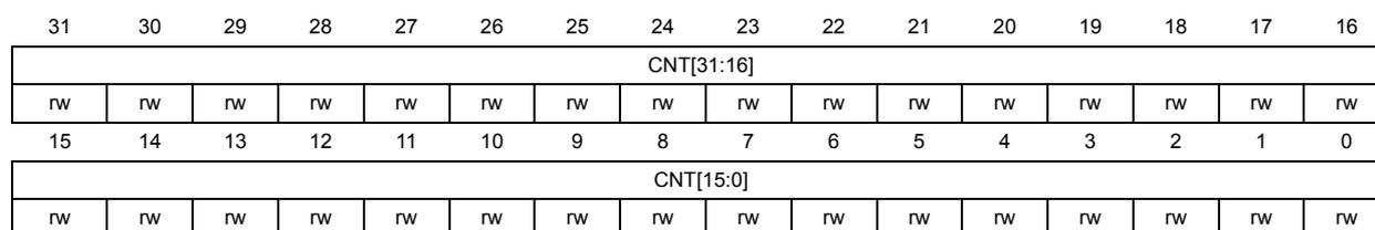
| 31 | 30 | 29 | 28 | 27 | 26 | 25 | 24 | 23 | 22 | 21 | 20 | 19 | 18 | 17 | 16 |
| CNT[31:16] | |||||||||||||||
| rw | rw | rw | rw | rw | rw | rw | rw | rw | rw | rw | rw | rw | rw | rw | rw |
| 15 | 14 | 13 | 12 | 11 | 10 | 9 | 8 | 7 | 6 | 5 | 4 | 3 | 2 | 1 | 0 |
| CNT[15:0] | |||||||||||||||
| rw | rw | rw | rw | rw | rw | rw | rw | rw | rw | rw | rw | rw | rw | rw | rw |
Bits 31:16 CNT[31:16] : Most significant part counter value (TIM2 and TIM5)
Bits 15:0 CNT[15:0] : Least significant part of counter value
34.4.13 TIMx counter [alternate] (TIMx_CNT)(x = 2 to 5)
Bit 31 of this register has two possible definitions depending on the value of UIFREMAP in TIMx_CR1 register:
- • Previous section is for UIFREMAP = 0
- • This section is for UIFREMAP = 1
Address offset: 0x24
Reset value: 0x0000 0000
| 31 | 30 | 29 | 28 | 27 | 26 | 25 | 24 | 23 | 22 | 21 | 20 | 19 | 18 | 17 | 16 |
| UIFCPY | CNT[30:16] | ||||||||||||||
| rw | rw | rw | rw | rw | rw | rw | rw | rw | rw | rw | rw | rw | rw | rw | rw |
| 15 | 14 | 13 | 12 | 11 | 10 | 9 | 8 | 7 | 6 | 5 | 4 | 3 | 2 | 1 | 0 |
| CNT[15:0] | |||||||||||||||
| rw | rw | rw | rw | rw | rw | rw | rw | rw | rw | rw | rw | rw | rw | rw | rw |
Bit 31 UIFCPY : UIF Copy
This bit is a read-only copy of the UIF bit of the TIMx_ISR register
Bits 30:16 CNT[30:16] : Most significant part counter value (TIM2 and TIM5)
Bits 15:0 CNT[15:0] : Least significant part of counter value
34.4.14 TIMx prescaler (TIMx_PSC)(x = 2 to 5)
Address offset: 0x28
Reset value: 0x0000

| 15 | 14 | 13 | 12 | 11 | 10 | 9 | 8 | 7 | 6 | 5 | 4 | 3 | 2 | 1 | 0 |
| PSC[15:0] | |||||||||||||||
| rw | rw | rw | rw | rw | rw | rw | rw | rw | rw | rw | rw | rw | rw | rw | rw |
Bits 15:0 PSC[15:0] : Prescaler value
The counter clock frequency CK_CNT is equal to \( f_{CK\_PSC} / (PSC[15:0] + 1) \) .
PSC contains the value to be loaded in the active prescaler register at each update event (including when the counter is cleared through UG bit of TIMx_EGR register or through trigger controller when configured in ‘‘reset mode’’).
34.4.15 TIMx auto-reload register (TIMx_ARR)(x = 2 to 5)
Address offset: 0x2C
Reset value: 0xFFFF FFFF
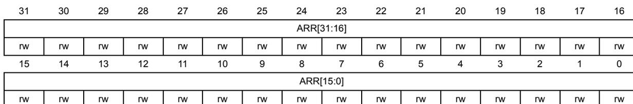
| 31 | 30 | 29 | 28 | 27 | 26 | 25 | 24 | 23 | 22 | 21 | 20 | 19 | 18 | 17 | 16 |
| ARR[31:16] | |||||||||||||||
| rw | rw | rw | rw | rw | rw | rw | rw | rw | rw | rw | rw | rw | rw | rw | rw |
| 15 | 14 | 13 | 12 | 11 | 10 | 9 | 8 | 7 | 6 | 5 | 4 | 3 | 2 | 1 | 0 |
| ARR[15:0] | |||||||||||||||
| rw | rw | rw | rw | rw | rw | rw | rw | rw | rw | rw | rw | rw | rw | rw | rw |
Bits 31:16 ARR[31:16] : High auto-reload value (TIM2 and TIM5)
Bits 15:0 ARR[15:0] : Low Auto-reload value
ARR is the value to be loaded in the actual auto-reload register.
Refer to the Section 34.3.1: Time-base unit on page 1179 for more details about ARR update and behavior.
The counter is blocked while the auto-reload value is null.
34.4.16 TIMx capture/compare register 1 (TIMx_CCR1)(x = 2 to 5)
Address offset: 0x34
Reset value: 0x0000 0000
| 31 | 30 | 29 | 28 | 27 | 26 | 25 | 24 | 23 | 22 | 21 | 20 | 19 | 18 | 17 | 16 |
| CCR1[31:16] | |||||||||||||||
| rw | rw | rw | rw | rw | rw | rw | rw | rw | rw | rw | rw | rw | rw | rw | rw |
| 15 | 14 | 13 | 12 | 11 | 10 | 9 | 8 | 7 | 6 | 5 | 4 | 3 | 2 | 1 | 0 |
| CCR1[15:0] | |||||||||||||||
| rw | rw | rw | rw | rw | rw | rw | rw | rw | rw | rw | rw | rw | rw | rw | rw |
Bits 31:16 CCR1[31:16] : High Capture/Compare 1 value (TIM2 and TIM5)
Bits 15:0 CCR1[15:0] : Low Capture/Compare 1 value
If channel CC1 is configured as output:
CCR1 is the value to be loaded in the actual capture/compare 1 register (preload value).
It is loaded permanently if the preload feature is not selected in the TIMx_CCMR1 register (bit OC1PE). Else the preload value is copied in the active capture/compare 1 register when an update event occurs.
The active capture/compare register contains the value to be compared to the counter TIMx_CNT and signaled on OC1 output.
If channel CC1 is configured as input:
CCR1 is the counter value transferred by the last input capture 1 event (IC1). The TIMx_CCR1 register is read-only and cannot be programmed.
34.4.17 TIMx capture/compare register 2 (TIMx_CCR2)(x = 2 to 5)
Address offset: 0x38
Reset value: 0x0000 0000
| 31 | 30 | 29 | 28 | 27 | 26 | 25 | 24 | 23 | 22 | 21 | 20 | 19 | 18 | 17 | 16 |
| CCR2[31:16] | |||||||||||||||
| rw | rw | rw | rw | rw | rw | rw | rw | rw | rw | rw | rw | rw | rw | rw | rw |
| 15 | 14 | 13 | 12 | 11 | 10 | 9 | 8 | 7 | 6 | 5 | 4 | 3 | 2 | 1 | 0 |
| CCR2[15:0] | |||||||||||||||
| rw | rw | rw | rw | rw | rw | rw | rw | rw | rw | rw | rw | rw | rw | rw | rw |
Bits 31:16 CCR2[31:16] : High Capture/Compare 2 value (TIM2 and TIM5)
Bits 15:0 CCR2[15:0] : Low Capture/Compare 2 value
If channel CC2 is configured as output:
CCR2 is the value to be loaded in the actual capture/compare 2 register (preload value). It is loaded permanently if the preload feature is not selected in the TIMx_CCMR1 register (bit OC2PE). Else the preload value is copied in the active capture/compare 2 register when an update event occurs.
The active capture/compare register contains the value to be compared to the counter TIMx_CNT and signalled on OC2 output.
If channel CC2 is configured as input:
CCR2 is the counter value transferred by the last input capture 2 event (IC2). The TIMx_CCR2 register is read-only and cannot be programmed.
34.4.18 TIMx capture/compare register 3 (TIMx_CCR3)(x = 2 to 5)
Address offset: 0x3C
Reset value: 0x0000 0000
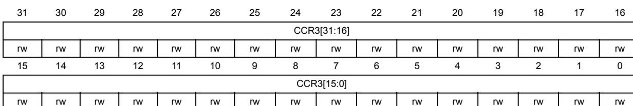
| 31 | 30 | 29 | 28 | 27 | 26 | 25 | 24 | 23 | 22 | 21 | 20 | 19 | 18 | 17 | 16 |
| CCR3[31:16] | |||||||||||||||
| rw | rw | rw | rw | rw | rw | rw | rw | rw | rw | rw | rw | rw | rw | rw | rw |
| 15 | 14 | 13 | 12 | 11 | 10 | 9 | 8 | 7 | 6 | 5 | 4 | 3 | 2 | 1 | 0 |
| CCR3[15:0] | |||||||||||||||
| rw | rw | rw | rw | rw | rw | rw | rw | rw | rw | rw | rw | rw | rw | rw | rw |
Bits 31:16 CCR3[31:16] : High Capture/Compare 3 value (TIM2 and TIM5)
Bits 15:0 CCR3[15:0] : Low Capture/Compare value
If channel CC3 is configured as output:
CCR3 is the value to be loaded in the actual capture/compare 3 register (preload value). It is loaded permanently if the preload feature is not selected in the TIMx_CCMR2 register (bit OC3PE). Else the preload value is copied in the active capture/compare 3 register when an update event occurs.
The active capture/compare register contains the value to be compared to the counter TIMx_CNT and signalled on OC3 output.
If channel CC3 is configured as input:
CCR3 is the counter value transferred by the last input capture 3 event (IC3). The TIMx_CCR3 register is read-only and cannot be programmed.
34.4.19 TIMx capture/compare register 4 (TIMx_CCR4)(x = 2 to 5)
Address offset: 0x40
Reset value: 0x0000 0000
| 31 | 30 | 29 | 28 | 27 | 26 | 25 | 24 | 23 | 22 | 21 | 20 | 19 | 18 | 17 | 16 |
|---|---|---|---|---|---|---|---|---|---|---|---|---|---|---|---|
| CCR4[31:16] | |||||||||||||||
| rw | rw | rw | rw | rw | rw | rw | rw | rw | rw | rw | rw | rw | rw | rw | rw |
| 15 | 14 | 13 | 12 | 11 | 10 | 9 | 8 | 7 | 6 | 5 | 4 | 3 | 2 | 1 | 0 |
| CCR4[15:0] | |||||||||||||||
| rw | rw | rw | rw | rw | rw | rw | rw | rw | rw | rw | rw | rw | rw | rw | rw |
Bits 31:16 CCR4[31:16] : High Capture/Compare 4 value (TIM2 and TIM5)
Bits 15:0 CCR4[15:0] : Low Capture/Compare value
- 1. if CC4 channel is configured as output (CC4S bits):
CCR4 is the value to be loaded in the actual capture/compare 4 register (preload value). It is loaded permanently if the preload feature is not selected in the TIMx_CCMR2 register (bit OC4PE). Else the preload value is copied in the active capture/compare 4 register when an update event occurs.
The active capture/compare register contains the value to be compared to the counter TIMx_CNT and signalled on OC4 output. - 2. if CC4 channel is configured as input (CC4S bits in TIMx_CCMR4 register):
CCR4 is the counter value transferred by the last input capture 4 event (IC4). The TIMx_CCR4 register is read-only and cannot be programmed.
34.4.20 TIMx DMA control register (TIMx_DCR)(x = 2 to 5)
Address offset: 0x48
Reset value: 0x0000
| 15 | 14 | 13 | 12 | 11 | 10 | 9 | 8 | 7 | 6 | 5 | 4 | 3 | 2 | 1 | 0 |
|---|---|---|---|---|---|---|---|---|---|---|---|---|---|---|---|
| Res. | Res. | Res. | DBL[4:0] | Res. | Res. | Res. | DBA[4:0] | ||||||||
| rw | rw | rw | rw | rw | rw | rw | rw | rw | rw | ||||||
Bits 15:13 Reserved, must be kept at reset value.
Bits 12:8 DBL[4:0] : DMA burst length
This 5-bit vector defines the number of DMA transfers (the timer recognizes a burst transfer when a read or a write access is done to the TIMx_DMAR address).
00000: 1 transfer,
00001: 2 transfers,
00010: 3 transfers,
...
10001: 18 transfers.
Bits 7:5 Reserved, must be kept at reset value.
Bits 4:0 DBA[4:0] : DMA base address
This 5-bit vector defines the base-address for DMA transfers (when read/write access are done through the TIMx_DMAR address). DBA is defined as an offset starting from the address of the TIMx_CR1 register.
Example:
00000: TIMx_CR1
00001: TIMx_CR2
00010: TIMx_SMCR
...
Example: Let us consider the following transfer: DBL = 7 transfers & DBA = TIMx_CR1. In this case the transfer is done to/from 7 registers starting from the TIMx_CR1 address.
34.4.21 TIMx DMA address for full transfer (TIMx_DMAR)(x = 2 to 5)
Address offset: 0x4C
Reset value: 0x0000
| 15 | 14 | 13 | 12 | 11 | 10 | 9 | 8 | 7 | 6 | 5 | 4 | 3 | 2 | 1 | 0 |
|---|---|---|---|---|---|---|---|---|---|---|---|---|---|---|---|
| DMAB[15:0] | |||||||||||||||
| rw | rw | rw | rw | rw | rw | rw | rw | rw | rw | rw | rw | rw | rw | rw | rw |
Bits 15:0 DMAB[15:0] : DMA register for burst accesses
A read or write operation to the DMAR register accesses the register located at the address
where TIMx_CR1 address is the address of the control register 1, DBA is the DMA base address configured in TIMx_DCR register, DMA index is automatically controlled by the DMA transfer, and ranges from 0 to DBL (DBL configured in TIMx_DCR).
34.4.22 TIM2 option register 1 (TIM2_OR1)
Address offset: 0x50
Reset value: 0x0000 0000
| 31 | 30 | 29 | 28 | 27 | 26 | 25 | 24 | 23 | 22 | 21 | 20 | 19 | 18 | 17 | 16 |
|---|---|---|---|---|---|---|---|---|---|---|---|---|---|---|---|
| Res. | Res. | Res. | Res. | Res. | Res. | Res. | Res. | Res. | Res. | Res. | Res. | Res. | Res. | Res. | Res. |
| 15 | 14 | 13 | 12 | 11 | 10 | 9 | 8 | 7 | 6 | 5 | 4 | 3 | 2 | 1 | 0 |
| Res. | TI4_RMP[1:0] | ETR_RMP | ITR1_RMP | ||||||||||||
| rw | rw | rw | rw | ||||||||||||
Bits 31:4 Reserved, must be kept at reset value.
Bits 3:2 TI4_RMP[1:0] : Input Capture 4 remap
- 00: TIM2 input capture 4 is connected to I/O
- 01: TIM2 input capture 4 is connected to COMP1_OUT
- 10: TIM2 input capture 4 is connected to COMP2_OUT
- 11: TIM2 input capture 4 is connected to logical OR between COMP1_OUT and COMP2_OUT
Bit 1 ETR_RMP : External trigger remap
- 0: TIM2_ETR is connected to I/O
- 1: TIM2_ETR is connected to LSE
Bit 0 ITR1_RMP : Internal trigger 1 remap
- 0: TIM2_ITR1 is connected to TIM8_TRGO
- 1: TIM2_ITR1 is connected to USB_SOF
34.4.23 TIM3 option register 1 (TIM3_OR1)
Address offset: 0x50
Reset value: 0x0000 0000
| 31 | 30 | 29 | 28 | 27 | 26 | 25 | 24 | 23 | 22 | 21 | 20 | 19 | 18 | 17 | 16 |
|---|---|---|---|---|---|---|---|---|---|---|---|---|---|---|---|
| Res. | Res. | Res. | Res. | Res. | Res. | Res. | Res. | Res. | Res. | Res. | Res. | Res. | Res. | Res. | Res. |
| 15 | 14 | 13 | 12 | 11 | 10 | 9 | 8 | 7 | 6 | 5 | 4 | 3 | 2 | 1 | 0 |
| Res. | Res. | Res. | Res. | Res. | Res. | Res. | Res. | Res. | Res. | Res. | Res. | Res. | Res. | TI1_RMP[1:0] | |
| rw | rw | ||||||||||||||
Bits 31:2 Reserved, must be kept at reset value.
Bits 1:0 TI1_RMP[1:0] : Input Capture 1 remap
- 00: TIM3 input capture 1 is connected to I/O
- 01: TIM3 input capture 1 is connected to COMP1_OUT
- 10: TIM3 input capture 1 is connected to COMP2_OUT
- 11: TIM3 input capture 1 is connected to logical OR between COMP1_OUT and COMP2_OUT
34.4.24 TIM2 option register 2 (TIM2_OR2)
Address offset: 0x60
Reset value: 0x0000 0000
| 31 | 30 | 29 | 28 | 27 | 26 | 25 | 24 | 23 | 22 | 21 | 20 | 19 | 18 | 17 | 16 |
|---|---|---|---|---|---|---|---|---|---|---|---|---|---|---|---|
| Res. | Res. | Res. | Res. | Res. | Res. | Res. | Res. | Res. | Res. | Res. | Res. | Res. | Res. | Res. | ETR SEL2 |
| rw | |||||||||||||||
| 15 | 14 | 13 | 12 | 11 | 10 | 9 | 8 | 7 | 6 | 5 | 4 | 3 | 2 | 1 | 0 |
| ETRSEL[1:0] | Res. | Res. | Res. | Res. | Res. | Res. | Res. | Res. | Res. | Res. | Res. | Res. | Res. | Res. | |
| rw | rw | ||||||||||||||
Bits 31:17 Reserved, must be kept at reset value.
Bits 16:14 ETRSEL[2:0] : ETR source selection
These bits select the ETR input source.
- 000: TIM2_ETR source is selected with the ETR_RMP bitfield in TIM2_OR1 register
- 001: COMP1 output connected to ETR input
- 010: COMP2 output connected to ETR input
- Others: Reserved
Bits 13:0 Reserved, must be kept at reset value.
34.4.25 TIM3 option register 2 (TIM3_OR2)
Address offset: 0x60
Reset value: 0x0000 0000
| 31 | 30 | 29 | 28 | 27 | 26 | 25 | 24 | 23 | 22 | 21 | 20 | 19 | 18 | 17 | 16 |
|---|---|---|---|---|---|---|---|---|---|---|---|---|---|---|---|
| Res. | Res. | Res. | Res. | Res. | Res. | Res. | Res. | Res. | Res. | Res. | Res. | Res. | Res. | Res. | ETR SEL2 |
| rw | |||||||||||||||
| 15 | 14 | 13 | 12 | 11 | 10 | 9 | 8 | 7 | 6 | 5 | 4 | 3 | 2 | 1 | 0 |
|---|---|---|---|---|---|---|---|---|---|---|---|---|---|---|---|
| ETRSEL[1:0] | Res. | Res. | Res. | Res. | Res. | Res. | Res. | Res. | Res. | Res. | Res. | Res. | Res. | Res. | |
| rw | rw | ||||||||||||||
Bits 31:17 Reserved, must be kept at reset value.
Bits 16:14 ETRSEL[2:0] : ETR source selection
These bits select the ETR input source.
000: ETR input is connected to I/O
001: COMP1 output connected to ETR input
Others: Reserved
Bits 13:0 Reserved, must be kept at reset value.
34.4.26 TIMx register map
TIMx registers are mapped as described in the table below:
Table 287. TIM2/TIM3/TIM4/TIM5 register map and reset values
| Offset | Register name | 31 | 30 | 29 | 28 | 27 | 26 | 25 | 24 | 23 | 22 | 21 | 20 | 19 | 18 | 17 | 16 | 15 | 14 | 13 | 12 | 11 | 10 | 9 | 8 | 7 | 6 | 5 | 4 | 3 | 2 | 1 | 0 |
|---|---|---|---|---|---|---|---|---|---|---|---|---|---|---|---|---|---|---|---|---|---|---|---|---|---|---|---|---|---|---|---|---|---|
| 0x00 | TIMx_CR1 | Res | Res | Res | Res | Res | Res | Res | Res | Res | Res | Res | Res | Res | Res | Res | Res | Res | Res | Res | Res | UIFREMA | Res | CKD [1:0] | ARPE | CMS [1:0] | DIR | OPM | URS | UDIS | CEN | ||
| Reset value | 0 | 0 | 0 | 0 | 0 | 0 | 0 | 0 | 0 | 0 | |||||||||||||||||||||||
| 0x04 | TIMx_CR2 | Res | Res | Res | Res | Res | Res | Res | Res | Res | Res | Res | Res | Res | Res | Res | Res | Res | Res | Res | Res | Res | Res | Res | Res | TI1S | MMS[2:0] | CCDS | Res | Res | Res | Res | Res |
| Reset value | 0 | 0 | 0 | 0 | 0 | ||||||||||||||||||||||||||||
| 0x08 | TIMx_SMCR | Res | Res | Res | Res | Res | Res | Res | Res | Res | Res | Res | Res | Res | Res | Res | SMS[3] | ETP | ECE | ETPS [1:0] | ETF[3:0] | MSM | TS[2:0] | Res | Res | Res | Res | Res | Res | Res | SMS[2:0] | Res | Res |
| Reset value | 0 | 0 | 0 | 0 | 0 | 0 | 0 | 0 | 0 | 0 | 0 | 0 | 0 | 0 | 0 | 0 | |||||||||||||||||
| 0x0C | TIMx_DIER | Res | Res | Res | Res | Res | Res | Res | Res | Res | Res | Res | Res | Res | Res | Res | Res | Res | TDE | Res | CC4DE | CC3DE | CC2DE | CC1DE | UDE | Res | TIE | Res | CC4IE | CC3IE | CC2IE | CC1IE | UIE |
| Reset value | 0 | 0 | 0 | 0 | 0 | 0 | 0 | 0 | 0 | 0 | 0 | 0 | 0 | ||||||||||||||||||||
| 0x10 | TIMx_SR | Res | Res | Res | Res | Res | Res | Res | Res | Res | Res | Res | Res | Res | Res | Res | Res | Res | Res | Res | CC4OF | CC3OF | CC2OF | CC1OF | Res | TIF | Res | CC4IF | CC3IF | CC2IF | CC1IF | UIF | |
| Reset value | 0 | 0 | 0 | 0 | 0 | 0 | 0 | 0 | 0 | 0 | 0 | 0 | |||||||||||||||||||||
| 0x14 | TIMx_EGR | Res | Res | Res | Res | Res | Res | Res | Res | Res | Res | Res | Res | Res | Res | Res | Res | Res | Res | Res | Res | Res | Res | Res | Res | TG | Res | CC4G | CC3G | CC2G | CC1G | UG | |
| Reset value | 0 | 0 | 0 | 0 | 0 | 0 | |||||||||||||||||||||||||||
| 0x18 | TIMx_CCMR1 Output Compare mode | Res | Res | Res | Res | Res | Res | Res | OC2M[3] | Res | Res | Res | Res | Res | Res | Res | OC1M[3] | OC2CE | OC2M [2:0] | Res | OC2PE | OC2FE | CC2S [1:0] | OC1CE | OC1M [2:0] | Res | OC1PE | OC1FE | CC1S [1:0] | Res | Res | Res | Res |
| Reset value | 0 | 0 | 0 | 0 | 0 | 0 | 0 | 0 | 0 | 0 | 0 | 0 | 0 | 0 | 0 | 0 | 0 | ||||||||||||||||
| TIMx_CCMR1 Input Capture mode | Res | Res | Res | Res | Res | Res | Res | Res | Res | Res | Res | Res | Res | Res | Res | Res | IC2F[3:0] | IC2PSC [1:0] | CC2S [1:0] | IC1F[3:0] | IC1PSC [1:0] | CC1S [1:0] | Res | Res | Res | Res | Res | Res | Res | Res | Res | Res | |
| Reset value | 0 | 0 | 0 | 0 | 0 | 0 | 0 | 0 | 0 | 0 | 0 | 0 | 0 | 0 | 0 | ||||||||||||||||||
| 0x1C | TIMx_CCMR2 Output Compare mode | Res | Res | Res | Res | Res | Res | Res | OC4M[3] | Res | Res | Res | Res | Res | Res | Res | OC3M[3] | OC4CE | OC4M [2:0] | Res | OC4PE | OC4FE | CC4S [1:0] | OC3CE | OC3M [2:0] | Res | OC3PE | OC3FE | CC3S [1:0] | Res | Res | Res | Res |
| Reset value | 0 | 0 | 0 | 0 | 0 | 0 | 0 | 0 | 0 | 0 | 0 | 0 | 0 | 0 | 0 | 0 | 0 | ||||||||||||||||
| TIMx_CCMR2 Input Capture mode | Res | Res | Res | Res | Res | Res | Res | Res | Res | Res | Res | Res | Res | Res | Res | Res | IC4F[3:0] | IC4PSC [1:0] | CC4S [1:0] | IC3F[3:0] | IC3PSC [1:0] | CC3S [1:0] | Res | Res | Res | Res | Res | Res | Res | Res | Res | Res | |
| Reset value | 0 | 0 | 0 | 0 | 0 | 0 | 0 | 0 | 0 | 0 | 0 | 0 | 0 | 0 | 0 | ||||||||||||||||||
| 0x20 | TIMx_CCER | Res | Res | Res | Res | Res | Res | Res | Res | Res | Res | Res | Res | Res | Res | Res | CC4NP | Res | CC4P | CC4E | CC3NP | Res | CC3P | CC3E | CC2NP | Res | CC2P | CC2E | CC1NP | Res | CC1P | CC1E | |
| Reset value | 0 | 0 | 0 | 0 | 0 | 0 | 0 | 0 | 0 | 0 | 0 | 0 |
Table 287. TIM2/TIM3/TIM4/TIM5 register map and reset values (continued)
| Offset | Register name | 31 | 30 | 29 | 28 | 27 | 26 | 25 | 24 | 23 | 22 | 21 | 20 | 19 | 18 | 17 | 16 | 15 | 14 | 13 | 12 | 11 | 10 | 9 | 8 | 7 | 6 | 5 | 4 | 3 | 2 | 1 | 0 |
|---|---|---|---|---|---|---|---|---|---|---|---|---|---|---|---|---|---|---|---|---|---|---|---|---|---|---|---|---|---|---|---|---|---|
| 0x24 | TIMx_CNT | CNT[31] or UIFCPY | CNT[30:16] (TIM2 and TIM5 only, reserved on the other timers) | CNT[15:0] | |||||||||||||||||||||||||||||
| Reset value | 0 | 0 | 0 | 0 | 0 | 0 | 0 | 0 | 0 | 0 | 0 | 0 | 0 | 0 | 0 | 0 | 0 | 0 | 0 | 0 | 0 | 0 | 0 | 0 | 0 | 0 | 0 | 0 | 0 | 0 | 0 | 0 | |
| 0x28 | TIMx_PSC | Res. | PSC[15:0] | ||||||||||||||||||||||||||||||
| Reset value | 0 | 0 | 0 | 0 | 0 | 0 | 0 | 0 | 0 | 0 | 0 | 0 | 0 | 0 | 0 | 0 | |||||||||||||||||
| 0x2C | TIMx_ARR | ARR[31:16] (TIM2 and TIM5 only, reserved on the other timers) | ARR[15:0] | ||||||||||||||||||||||||||||||
| Reset value | 1 | 1 | 1 | 1 | 1 | 1 | 1 | 1 | 1 | 1 | 1 | 1 | 1 | 1 | 1 | 1 | 1 | 1 | 1 | 1 | 1 | 1 | 1 | 1 | 1 | 1 | 1 | 1 | 1 | 1 | 1 | 1 | |
| 0x30 | Reserved | ||||||||||||||||||||||||||||||||
| 0x34 | TIMx_CCR1 | CCR1[31:16] (TIM2 and TIM5 only, reserved on the other timers) | CCR1[15:0] | ||||||||||||||||||||||||||||||
| Reset value | 0 | 0 | 0 | 0 | 0 | 0 | 0 | 0 | 0 | 0 | 0 | 0 | 0 | 0 | 0 | 0 | 0 | 0 | 0 | 0 | 0 | 0 | 0 | 0 | 0 | 0 | 0 | 0 | 0 | 0 | 0 | 0 | |
| 0x38 | TIMx_CCR2 | CCR2[31:16] (TIM2 and TIM5 only, reserved on the other timers) | CCR2[15:0] | ||||||||||||||||||||||||||||||
| Reset value | 0 | 0 | 0 | 0 | 0 | 0 | 0 | 0 | 0 | 0 | 0 | 0 | 0 | 0 | 0 | 0 | 0 | 0 | 0 | 0 | 0 | 0 | 0 | 0 | 0 | 0 | 0 | 0 | 0 | 0 | 0 | 0 | |
| 0x3C | TIMx_CCR3 | CCR3[31:16] (TIM2 and TIM5 only, reserved on the other timers) | CCR3[15:0] | ||||||||||||||||||||||||||||||
| Reset value | 0 | 0 | 0 | 0 | 0 | 0 | 0 | 0 | 0 | 0 | 0 | 0 | 0 | 0 | 0 | 0 | 0 | 0 | 0 | 0 | 0 | 0 | 0 | 0 | 0 | 0 | 0 | 0 | 0 | 0 | 0 | 0 | |
| 0x40 | TIMx_CCR4 | CCR4[31:16] (TIM2 and TIM5 only, reserved on the other timers) | CCR4[15:0] | ||||||||||||||||||||||||||||||
| Reset value | 0 | 0 | 0 | 0 | 0 | 0 | 0 | 0 | 0 | 0 | 0 | 0 | 0 | 0 | 0 | 0 | 0 | 0 | 0 | 0 | 0 | 0 | 0 | 0 | 0 | 0 | 0 | 0 | 0 | 0 | 0 | 0 | |
| 0x44 | Reserved | ||||||||||||||||||||||||||||||||
| 0x48 | TIMx_DCR | Res. | DBL[4:0] | Res. | DBA[4:0] | ||||||||||||||||||||||||||||
| Reset value | 0 | 0 | 0 | 0 | 0 | 0 | 0 | 0 | 0 | 0 | |||||||||||||||||||||||
| 0x4C | TIMx_DMAR | Res. | DMAB[15:0] | ||||||||||||||||||||||||||||||
| Reset value | 0 | 0 | 0 | 0 | 0 | 0 | 0 | 0 | 0 | 0 | 0 | 0 | 0 | 0 | 0 | 0 | |||||||||||||||||
| 0x50 | TIM2_OR1 | Res. | TI4_RMP[1:0] | ETR_RMP | ITR1_RMP | ||||||||||||||||||||||||||||
| Reset value | 0 | 0 | 0 | 0 | |||||||||||||||||||||||||||||
Table 287. TIM2/TIM3/TIM4/TIM5 register map and reset values (continued)
| Offset | Register name | 31 | 30 | 29 | 28 | 27 | 26 | 25 | 24 | 23 | 22 | 21 | 20 | 19 | 18 | 17 | 16 | 15 | 14 | 13 | 12 | 11 | 10 | 9 | 8 | 7 | 6 | 5 | 4 | 3 | 2 | 1 | 0 | |
|---|---|---|---|---|---|---|---|---|---|---|---|---|---|---|---|---|---|---|---|---|---|---|---|---|---|---|---|---|---|---|---|---|---|---|
| 0x50 | TIM3_OR1 | Res. | Res. | Res. | Res. | Res. | Res. | Res. | Res. | Res. | Res. | Res. | Res. | Res. | Res. | Res. | Res. | Res. | Res. | Res. | Res. | Res. | Res. | Res. | Res. | Res. | Res. | Res. | Res. | Res. | Res. | Res. | Res. | T11_RMP[1:0] |
| Reset value | 0 | |||||||||||||||||||||||||||||||||
| 0x60 | TIM2_OR2 | Res. | Res. | Res. | Res. | Res. | Res. | Res. | Res. | Res. | Res. | Res. | Res. | Res. | Res. | Res. | ETRSEL [2:0] | Res. | Res. | Res. | Res. | Res. | Res. | Res. | Res. | Res. | Res. | Res. | Res. | Res. | Res. | Res. | Res. | Res. |
| Reset value | 0 | 0 | 0 | |||||||||||||||||||||||||||||||
| 0x60 | TIM3_OR2 | Res. | Res. | Res. | Res. | Res. | Res. | Res. | Res. | Res. | Res. | Res. | Res. | Res. | Res. | Res. | ETRSEL [2:0] | Res. | Res. | Res. | Res. | Res. | Res. | Res. | Res. | Res. | Res. | Res. | Res. | Res. | Res. | Res. | Res. | Res. |
| Reset value | 0 | 0 | 0 |
Refer to Section 2.3 on page 86 for the register boundary addresses.