24. Comparator (COMP)
24.1 Introduction
The device embeds two ultra-low-power comparators COMP1, and COMP2
The comparators can be used for a variety of functions including:
- • Wake-up from low-power mode triggered by an analog signal,
- • Analog signal conditioning,
- • Cycle-by-cycle current control loop when combined with a PWM output from a timer.
24.2 COMP main features
- • Each comparator has configurable plus and minus inputs used for flexible voltage selection:
- – Multiplexed I/O pins
- – DAC Channel1 and Channel2
- – Internal reference voltage and three submultiple values (1/4, 1/2, 3/4) provided by scaler (buffered voltage divider)
- • Programmable hysteresis
- • Programmable speed / consumption
- • The outputs can be redirected to an I/O or to timer inputs for triggering:
- – Break events for fast PWM shutdowns
- • Comparator outputs with blanking source
- • The two comparators can be combined in a window comparator
- • Each comparator has interrupt generation capability with wake-up from Sleep and Stop modes (through the EXTI controller)
24.3 COMP functional description
24.3.1 COMP block diagram
The block diagram of the comparators is shown in Figure 172 .
Figure 172. Comparator block diagram
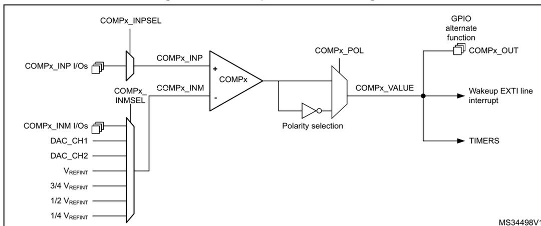
24.3.2 COMP pins and internal signals
The I/Os used as comparators inputs must be configured in analog mode in the GPIOs registers.
The comparator output can be connected to the I/Os using the alternate function channel given in “Alternate function mapping” table in the datasheet.
The output can also be internally redirected to a variety of timer input for the following purposes:
- • Emergency shut-down of PWM signals, using BKIN and BKIN2 inputs
- • Cycle-by-cycle current control, using OCREF_CLR inputs
- • Input capture for timing measures
It is possible to have the comparator output simultaneously redirected internally and externally.
Table 195. COMP1 input plus assignment
| COMP1_INP | COMP1_INPSEL [1:0] |
|---|---|
| PC5 | 00 |
| PB2 | 01 |
| PA2 | 10 |
Table 196. COMP1 input minus assignment
| COMP1_INM | COMP1_INMSEL[2:0] |
|---|---|
| \( \frac{1}{4} V_{REFINT} \) | 000 |
| \( \frac{1}{2} V_{REFINT} \) | 001 |
| \( \frac{3}{4} V_{REFINT} \) | 010 |
| \( V_{REFINT} \) | 011 |
| DAC Channel1 | 100 |
| DAC Channel2 | 101 |
| PB1 | 110 |
| PC4 | 111 |
Table 197. COMP2 input plus assignment
| COMP2_INP | COMP2_INPSEL |
|---|---|
| PB4 | 0 |
| PB6 | 1 |
Table 198. COMP2 input minus assignment
| COMP2_INM | COMP2_INMSEL[2:0] |
|---|---|
| \( \frac{1}{4} V_{REFINT} \) | 000 |
| \( \frac{1}{2} V_{REFINT} \) | 001 |
| \( \frac{3}{4} V_{REFINT} \) | 010 |
| \( V_{REFINT} \) | 011 |
| DAC Channel1 | 100 |
| DAC Channel2 | 101 |
| PB3 | 110 |
| PB7 | 111 |
24.3.3 COMP reset and clocks
The COMP clock provided by the clock controller is synchronous with the APB2 clock.
There is no clock enable control bit provided in the RCC controller. Reset and clock enable bits are common for COMP and SYSCFG.
Important: The polarity selection logic and the output redirection to the port works independently from the APB2 clock. This allows the comparator to work even in Stop mode.
24.3.4 Comparator LOCK mechanism
The comparators can be used for safety purposes, such as over-current or thermal protection. For applications having specific functional safety requirements, it is necessary to
insure that the comparator programming cannot be altered in case of spurious register access or program counter corruption.
For this purpose, the comparator control and status registers can be write-protected (read-only).
Once the programming is completed, the COMPx LOCK bit can be set to 1. This causes the whole register to become read-only, including the COMPx LOCK bit.
The write protection can only be reset by a MCU reset.
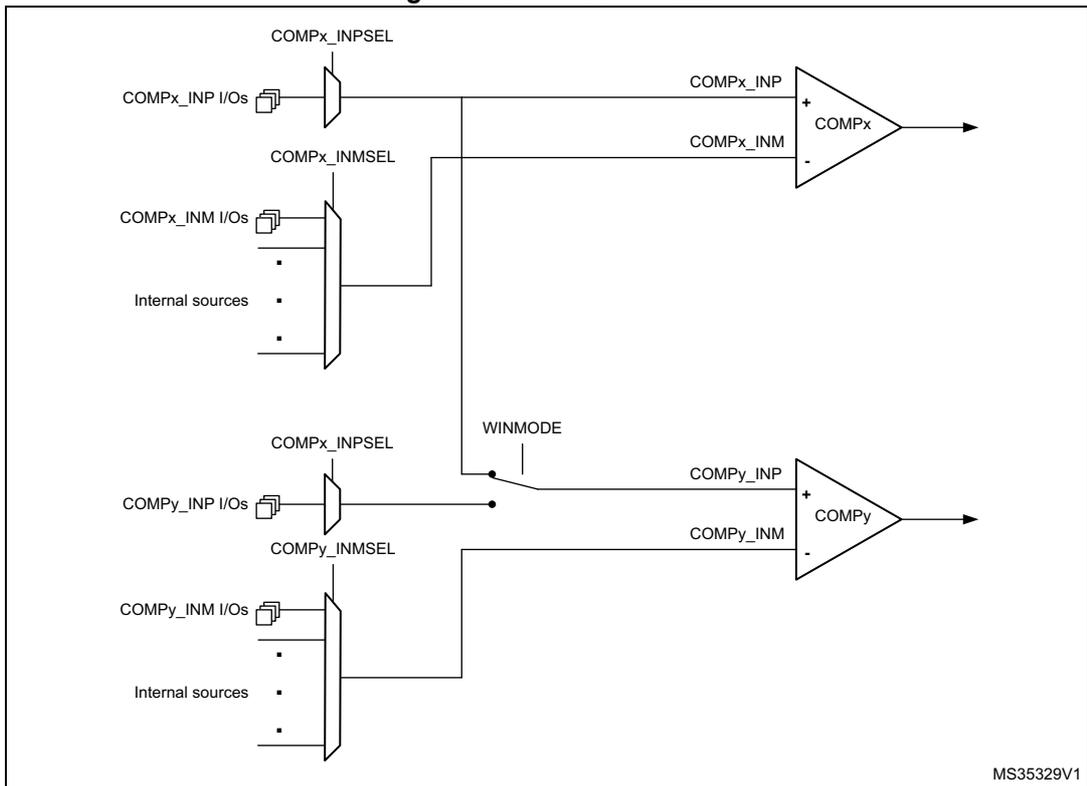
24.3.5 Window comparator
The purpose of window comparator is to monitor the analog voltage if it is within specified voltage range defined by lower and upper threshold.
Two embedded comparators can be utilized to create window comparator. The monitored analog voltage is connected to the non-inverting (plus) inputs of comparators connected together and the upper and lower threshold voltages are connected to the inverting (minus) inputs of the comparators. Two non-inverting inputs can be connected internally together by enabling WINMODE bit to save one IO for other purposes.
Figure 173. Window mode
24.3.6 Hysteresis
The comparator includes a programmable hysteresis to avoid spurious output transitions in case of noisy signals. The hysteresis can be disabled if it is not needed (for instance when exiting from low-power mode) to be able to force the hysteresis value using external components.
Figure 174. Comparator hysteresis
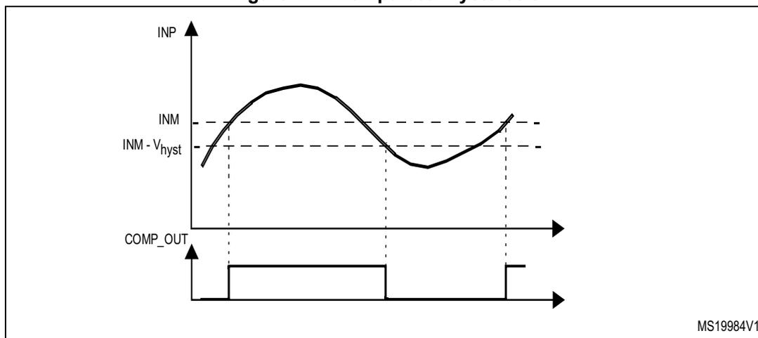
The diagram illustrates the hysteresis function of a comparator. The top waveform represents the non-inverting input (INP), which is a sinusoidal-like signal. The bottom waveform represents the comparator output (COMP_OUT), which is a digital signal. The output transitions between high and low states based on the input signal crossing specific threshold levels. The upper threshold is labeled INM, and the lower threshold is labeled INM - V hyst . Vertical dashed lines indicate the points where the input signal crosses these thresholds, corresponding to the output transitions. The identifier MS19984V1 is located in the bottom right corner.
24.3.7 Comparator output blanking function
The purpose of the blanking function is to prevent the current regulation to trip upon short current spikes at the beginning of the PWM period (typically the recovery current in power switches anti parallel diodes). It consists of a selection of a blanking window which is a timer output compare signal. The selection is done by software (refer to the comparator register description for possible blanking signals). Then, the complementary of the blanking signal is ANDed with the comparator output to provide the wanted comparator output. See the example provided in the figure below.
Figure 175. Comparator output blanking
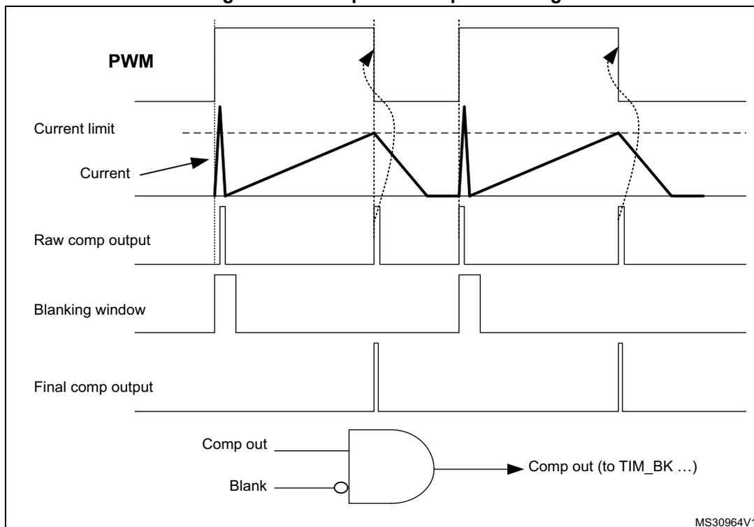
This diagram shows the comparator output blanking function. The top waveform is the PWM signal. Below it is the Current waveform, which shows a sharp initial spike followed by a sawtooth-like oscillation. The 'Raw comp output' shows pulses corresponding to the current spikes. The 'Blanking window' signal is a short pulse that coincides with the initial current spike. The 'Final comp output' is the result of ANDing the raw output with the inverted blanking window, effectively suppressing the initial spike. Below the waveforms, a logic diagram shows an AND gate with inputs 'Comp out' and 'Blank' (inverted). The output of the gate is labeled 'Comp out (to TIM_BK ...)'. The identifier MS30964V1 is located in the bottom right corner.
24.3.8 COMP power and speed modes
COMP1 and COMP2 power consumption versus propagation delay can be adjusted to have the optimum trade-off for a given application.
The bits PWRMODE[1:0] in COMPx_CSR registers can be programmed as follows:
00: High speed / full power
01 or 10: Medium speed / medium power
11: Low speed / ultra-low-power
24.4 COMP low-power modes
Table 199. Comparator behavior in the low power modes
| Mode | Description |
|---|---|
| Sleep | No effect on the comparators. Comparator interrupts cause the device to exit the Sleep mode. |
| Low-power run | No effect. |
| Low-power sleep | No effect. COMP interrupts cause the device to exit the Low-power sleep mode. |
| Stop 0 | No effect on the comparators. Comparator interrupts cause the device to exit the Stop mode. |
| Stop 1 | |
| Stop 2 | |
| Standby | The COMP registers are powered down and must be reinitialized after exiting Standby or Shutdown mode. |
| Shutdown |
24.5 COMP interrupts
The comparator outputs are internally connected to the Extended interrupts and events controller. Each comparator has its own EXTI line and can generate either interrupts or events. The same mechanism is used to exit from low-power modes.
Refer to Interrupt and events section for more details.
To enable COMPx interrupt, it is required to follow this sequence:
- 1. Configure and enable the EXTI line corresponding to the COMPx output event in interrupt mode and select the rising, falling or both edges sensitivity
- 2. Configure and enable the NVIC IRQ channel mapped to the corresponding EXTI lines
- 3. Enable COMPx.
Table 200. Interrupt control bits
| Interrupt event | Event flag | Enable control bit | Exit from Sleep mode | Exit from Stop modes | Exit from Standby mode |
|---|---|---|---|---|---|
| COMP1 output | VALUE in COMP1_CSR | Through EXTI | Yes | Yes | N/A |
| COMP2 output | VALUE in COMP2_CSR | Through EXTI | Yes | Yes | N/A |
24.6 COMP registers
24.6.1 Comparator 1 control and status register (COMP1_CSR)
The COMP1_CSR is the Comparator 1 control/status register. It contains all the bits /flags related to comparator1.
Address offset: 0x00
System reset value: 0x0000 0000
| 31 | 30 | 29 | 28 | 27 | 26 | 25 | 24 | 23 | 22 | 21 | 20 | 19 | 18 | 17 | 16 |
|---|---|---|---|---|---|---|---|---|---|---|---|---|---|---|---|
| LOCK | VALUE | Res. | Res. | Res. | Res. | Res. | Res. | SCAL EN | BRG EN | Res. | BLANKING[2:0] | HYST[1:0] | |||
| rs | r | rw | rw | rw | rw | rw | rw | rw | |||||||
| 15 | 14 | 13 | 12 | 11 | 10 | 9 | 8 | 7 | 6 | 5 | 4 | 3 | 2 | 1 | 0 |
|---|---|---|---|---|---|---|---|---|---|---|---|---|---|---|---|
| POLARITY | Res. | Res. | Res. | Res. | Res. | Res. | INP SEL[1:0] | INMSEL[2:0] | PWRMODE[1:0] | Res. | EN | ||||
| rw | rw | rw | rw | rw | rw | rw | rw | rw | |||||||
Bit 31 LOCK : COMP1_CSR register lock bit
This bit is set by software and cleared by a hardware system reset. It locks the whole content of the comparator 1 control register, COMP1_CSR[31:0].
0: COMP1_CSR[31:0] for comparator 1 are read/write
1: COMP1_CSR[31:0] for comparator 1 are read-only
Bit 30 VALUE : Comparator 1 output status bit
This bit is read-only. It reflects the current comparator 1 output taking into account POLARITY bit effect.
Bits 29: Reserved, must be kept at reset value.
Bit 23 SCALEN : Voltage scaler enable bit
This bit is set and cleared by software. This bit enable the outputs of the V REFINT divider available on the minus input of the Comparator 1.
0: Bandgap scaler disable (if SCALEN bit of COMP2_CSR register is also reset)
1: Bandgap scaler enable
Bit 22 BRGEN : Scaler bridge enable
This bit is set and cleared by software (only if LOCK not set). This bit enable the bridge of the scaler.
0: Scaler resistor bridge disable (if BRGEN bit of COMP2_CSR register is also reset)
1: Scaler resistor bridge enable
If SCALEN is set and BRGEN is reset, BG voltage reference is available but not 1/4 BGAP, 1/2 BGAP, 3/4 BGAP. BGAP value is sent instead of 1/4 BGAP, 1/2 BGAP, 3/4 BGAP.
If SCALEN and BRGEN are set, 1/4 BGAP 1/2 BGAP 3/4 BGAP and BGAP voltage references are available.
Bit 21 Reserved, must be kept at reset value.
Bits 20:18 BLANKING[2:0] : Comparator 1 blanking source selection bits
These bits select which timer output controls the comparator 1 output blanking.
000: No blanking
001: TIM1 OC5 selected as blanking source
010: TIM2 OC3 selected as blanking source
100: TIM3 OC3 selected as blanking source
All other values: reserved
Bits 17:16 HYST[1:0] : Comparator 1 hysteresis selection bits
These bits are set and cleared by software (only if LOCK not set). They select the hysteresis voltage of the comparator 1.
00: No hysteresis
01: Low hysteresis
10: Medium hysteresis
11: High hysteresis
Bit 15 POLARITY : Comparator 1 polarity selection bit
This bit is set and cleared by software (only if LOCK not set). It inverts Comparator 1 polarity.
0: Comparator 1 output value not inverted
1: Comparator 1 output value inverted
Bits 14:9 Reserved, must be kept at reset value.
Bits 8:7 INPSEL[1:0] : Comparator1 input plus selection bit
This bit is set and cleared by software (only if LOCK not set).
00: PC5
01: PB2
10: PA2
11: Reserved
Bits 6:4 INMSEL[2:0] : Comparator 1 input minus selection bits
These bits are set and cleared by software (only if LOCK not set). They select which input is connected to the input minus of comparator 1.
000 = 1/4 V REFINT
001 = 1/2 V REFINT
010 = 3/4 V REFINT
011 = V REFINT
100 = DAC Channel1
101 = DAC Channel2
110 = PB1111 = PC4
Bits 3:2 PWRMODE[1:0] : Power Mode of the comparator 1
These bits are set and cleared by software (only if LOCK not set). They control the power/speed of the Comparator 1.
00: High speed
01 or 10: Medium speed
11: Ultra low power
Bit 1 Reserved, must be kept at reset value.
Bit 0 EN : Comparator 1 enable bit
This bit is set and cleared by software (only if LOCK not set). It switches on Comparator1.
0: Comparator 1 switched OFF
1: Comparator 1 switched ON
24.6.2 Comparator 2 control and status register (COMP2_CSR)
The COMP2_CSR is the Comparator 2 control/status register. It contains all the bits /flags related to comparator 2.
Address offset: 0x04
System reset value: 0x0000 0000
| 31 | 30 | 29 | 28 | 27 | 26 | 25 | 24 | 23 | 22 | 21 | 20 | 19 | 18 | 17 | 16 |
|---|---|---|---|---|---|---|---|---|---|---|---|---|---|---|---|
| LOCK | VALUE | Res. | Res. | Res. | Res. | Res. | Res. | SCAL EN | BRG EN | Res. | BLANKING[2:0] | HYST[1:0] | |||
| rs | r | rw | rw | rw | rw | rw | rw | rw | |||||||
| 15 | 14 | 13 | 12 | 11 | 10 | 9 | 8 | 7 | 6 | 5 | 4 | 3 | 2 | 1 | 0 |
|---|---|---|---|---|---|---|---|---|---|---|---|---|---|---|---|
| POLA RITY | Res. | Res. | Res. | Res. | Res. | WIN MODE | Res. | INP SEL | INMSEL[2:0] | PWRMODE[1:0] | Res. | EN | |||
| rw | rw | rw | rw | rw | rw | rw | rw | rw | |||||||
Bit 31 LOCK : CSR register lock bit
This bit is set by software and cleared by a hardware system reset. It locks the whole content of the comparator 2 control register, COMP2_CSR[31:0].
0: COMP2_CSR[31:0] for comparator 2 are read/write
1: COMP2_CSR[31:0] for comparator 2 are read-only
Bit 30 VALUE : Comparator 2 output status bit
This bit is read-only. It reflects the current comparator 2 output taking into account POLARITY bit effect.
Bits 29:24 Reserved, must be kept at reset value.
Bit 23 SCALEN : Voltage scaler enable bit
This bit is set and cleared by software. This bit enable the outputs of the V REFINT divider available on the minus input of the Comparator 2.
0: Bandgap scaler disable (if SCALEN bit of COMP1_CSR register is also reset)
1: Bandgap scaler enable
This bit is set and cleared by software (only if LOCK not set). This bit enable the bridge of the scaler.
0: Scaler resistor bridge disable (if BRGEN bit of COMP1_CSR register is also reset)
1: Scaler resistor bridge enable
If SCALEN is set and BRGEN is reset, BG voltage reference is available but not 1/4 BGAP, 1/2 BGAP, 3/4 BGAP. BGAP value is sent instead of 1/4 BGAP, 1/2 BGAP, 3/4 BGAP.
If SCALEN and BRGEN are set, 1/4 BGAP 1/2 BGAP 3/4 BGAP and BGAP voltage references are available.
Bit 21 Reserved, must be kept at reset value.
Bits 20:18 BLANKING[2:0] : Comparator 2 blanking source selection bitsThese bits select which timer output controls the comparator 2 output blanking.
000: No blanking
001: TIM3 OC4 selected as blanking source
010: TIM8 OC5 selected as blanking source
100: TIM15 OC1 selected as blanking source
All other values: reserved
Bits 17:16 HYST[1:0] : Comparator 2 hysteresis selection bitsThese bits are set and cleared by software (only if LOCK not set). Select the hysteresis voltage of the comparator 2.
00: No hysteresis
01: Low hysteresis
10: Medium hysteresis
11: High hysteresis
Bit 15 POLARITY : Comparator 2 polarity selection bitThis bit is set and cleared by software (only if LOCK not set). It inverts Comparator 2 polarity.
0: Comparator 2 output value not inverted
1: Comparator 2 output value inverted
Bits 14:10 Reserved, must be kept at reset value.
Bit 9 WINMODE : Windows mode selection bitThis bit is set and cleared by software (only if LOCK not set). This bit selects the window mode of the comparators. If set, both positive inputs of comparators are connected together.
0: Input plus of Comparator 2 is not connected to Comparator 1
1: Input plus of Comparator 2 is connected with input plus of Comparator 1
Bit 8 Reserved, must be kept at reset value.
Bit 7 INPSEL : Comparator 1 input plus selection bitThis bit is set and cleared by software (only if LOCK not set).
0: PB4
1: PB6
Bits 6:4 INMSEL[2:0]: Comparator 2 input minus selection bitsThese bits are set and cleared by software (only if LOCK not set). They select which input is connected to the input minus of comparator 2.
000 = 1/4 V REFINT
001 = 1/2 V REFINT
010 = 3/4 V REFINT
011 = V REFINT
100 = DAC Channel1
101 = DAC Channel2
110 = PB3
111 = PB7
Bits 3:2 PWRRMODE[1:0]: Power Mode of the comparator 2These bits are set and cleared by software (only if LOCK not set). They control the power/speed of the Comparator 2.
00: High speed
01 or 10: Medium speed
11: Ultra low power
Bit 1 Reserved, must be kept at reset value.
Bit 0 EN: Comparator 2 enable bitThis bit is set and cleared by software (only if LOCK not set). It switches on comparator2.
0: Comparator 2 switched OFF
1: Comparator 2 switched ON
24.6.3 COMP register map
The following table summarizes the comparator registers.
Table 201. COMP register map and reset values
| Offset | Register | 31 | 30 | 29 | 28 | 27 | 26 | 25 | 24 | 23 | 22 | 21 | 20 | 19 | 18 | 17 | 16 | 15 | 14 | 13 | 12 | 11 | 10 | 9 | 8 | 7 | 6 | 5 | 4 | 3 | 2 | 1 | 0 |
|---|---|---|---|---|---|---|---|---|---|---|---|---|---|---|---|---|---|---|---|---|---|---|---|---|---|---|---|---|---|---|---|---|---|
| 0x00 | COMP1_CSR | LOCK | VALUE | Res. | Res. | Res. | Res. | Res. | Res. | SCALEN | BRGEN | Res. | BLANKING | HYST | POLARITY. | Res. | Res. | Res. | Res. | Res. | Res. | Res. | Res. | Res. | INPSEL. | INMSEL | PWRMODE | Res. | EN | ||||
| Reset value | 0 | 0 | 0 | 0 | |||||||||||||||||||||||||||||
| 0x04 | COMP2_CSR | LOCK | VALUE | Res. | Res. | Res. | Res. | Res. | Res. | SCALEN | BRGEN | Res. | BLANKING | HYST | POLARITY. | Res. | Res. | Res. | Res. | Res. | Res. | Res. | Res. | WINMODE | Res. | INPSEL | INMSEL | PWRMODE | Res. | EN | |||
| Reset value | 0 | 0 | 0 | 0 | 0 |
Refer to Section 2.3 on page 86 for the register boundary addresses.