9. Reset and clock control (RCC)
9.1 Reset
There are three types of reset:
- • a system reset
- • a power reset
- • a Backup domain reset
9.1.1 Power reset
A power reset is generated when one of the following events occurs:
- • a Brownout reset (BOR)
- • when exiting from Standby mode
- • when exiting from Shutdown mode
A Brownout reset, including power-on or power-down reset (POR/PDR), sets all registers to their reset values except the ones in the Backup domain.
When exiting Standby mode, all registers in the \( V_{CORE} \) domain are set to their reset value. Registers outside the \( V_{CORE} \) domain (RTC, WKUP, IWDG, and Standby/Shutdown modes control) are not impacted.
When exiting Shutdown mode, a Brownout reset is generated, resetting all registers except those in the Backup domain.
9.1.2 System reset
A system reset sets all registers to their reset values unless specified otherwise in the register description.
A system reset is generated when one of the following events occurs:
- • a low level on the NRST pin (external reset)
- • a window watchdog event (WWDG reset)
- • an independent watchdog event (IWDG reset)
- • a software reset (SW reset) (see Software reset )
- • a low-power mode security reset (see Low-power mode security reset )
- • an option byte loader reset (see Option byte loader reset )
- • a Brownout reset
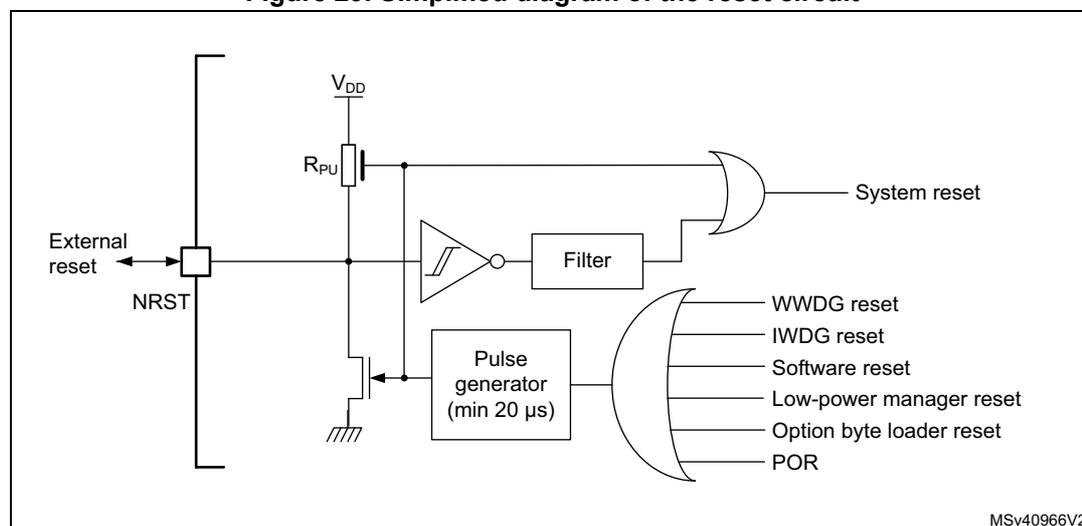
The reset source can be identified by checking the reset flags in RCC control/status register (RCC_CSR) .
These sources act on the NRST pin and this pin is always kept low during the delay phase. The reset service routine vector is selected via the Boot option bytes.
The system reset signal provided to the device is output on the NRST pin. The pulse generator guarantees a minimum reset pulse duration of 20 µs for each internal reset source. In case of an external reset, the reset pulse is generated while the NRST pin is asserted low.
In case of an internal reset, the internal pull-up \( R_{PU} \) is deactivated in order to save the power consumption through the pull-up resistor.
Figure 29. Simplified diagram of the reset circuit
Software reset
The SYSRESETREQ bit in Cortex ® -M33 application interrupt and reset control register must be set to force a software reset on the device.
Low-power mode security reset
To avoid that critical applications mistakenly enter a low-power mode, two low-power mode security resets are available. If enabled in option bytes, the resets are generated in any of the following conditions:
- • Entering Standby mode: this type of reset is enabled by resetting nRST_STDBY bit in user option bytes. In this case, whenever a Standby mode entry sequence is successfully executed, the device is reset instead of entering Standby mode.
- • Entering Stop mode: this type of reset is enabled by resetting nRST_STOP bit in user option bytes. In this case, whenever a Stop mode entry sequence is successfully executed, the device is reset instead of entering Stop mode.
- • Entering Shutdown mode: this type of reset is enabled by resetting nRST_SHDW bit in user option bytes. In this case, whenever a Shutdown mode entry sequence is successfully executed, the device is reset instead of entering Shutdown mode.
For further information on the user option bytes, refer to Section 6.4.1: Option bytes description .
Option byte loader reset
The option byte loader reset is generated when the OBL_LAUNCH bit (#27) is set in the FLASH_CR register. This bit is used to launch the option byte loading by software.
9.1.3 Backup domain reset
The Backup domain has two specific resets.
A Backup domain reset is generated when one of the following events occurs:
- • a software reset, triggered by setting the BDRST bit in the RCC Backup domain control register (RCC_BDCR)
- • a V DD or V BAT power on, if both supplies have previously been powered off
A Backup domain reset only affects the LSE oscillator, the RTC, the backup registers, the SRAM2 and the RCC_BDCR register.
9.2 RCC pins and internal signals
Table 78 lists the RCC inputs and output signals connected to package pins or balls.
Table 78. RCC input/output signals connected to package pins or balls
| Signal name | Signal type | Description |
|---|---|---|
| NRST | I/O | System reset, can be used to provide reset to external devices |
| OSC32_IN | I | 32 kHz oscillator input |
| OSC32_OUT | O | 32 kHz oscillator output |
| OSC_IN | I | System oscillator input |
| OSC_OUT | O | System oscillator output |
| MCO1 | O | Output clock 1 for external devices |
| SAI1_EXTCLK | I | External kernel clock input for SAI1 digital audio interface |
| SAI2_EXTCLK | I | External kernel clock input for SAI2 digital audio interface |
9.3 Clocks
Four different clock sources can be used to drive the system clock (SYSCLK):
- • HSI16 (high-speed internal) 16 MHz RC oscillator clock
- • MSI (multispeed internal) RC oscillator clock
- • HSE oscillator clock, from 4 to 48 MHz
- • PLL clock
The MSI is used as system clock source after startup from reset, configured at 4 MHz.
The devices have the following additional clock sources:
- • 32 kHz low-speed internal RC (LSI RC) that drives the independent watchdog and optionally the RTC used for auto-wakeup from Stop and Standby modes
- • 32.768 kHz low-speed external crystal (LSE crystal) that optionally drives the real-time clock (RTCCLK)
- • RC 48 MHz internal clock sources (HSI48) to potentially drive the USB FS, the SDMMC and the RNG
Each clock source can be switched on or off independently when it is not used, to optimize power consumption.
Several prescalers can be used to configure the AHB frequency, the APB1 and APB2 domains. The maximum frequency of the AHB, APB1 and APB2 domains is 110 MHz.
All the peripheral clocks are derived from their bus clock (HCLK, PCLK1 or PCLK2) except the following ones:
- • The 48 MHz clock used for USB FS, SDMMC and RNG, is derived from one of the following sources (selected by software):
- – main PLL VCO (PLL48M1CLK)
- – PLLSAI1 VCO (PLL48M2CLK)
- – MSI clock
- – HSI48 internal oscillator
When the MSI clock is auto-trimmed with the LSE, it can be used by the USB FS device.
When available, the HSI48 clock can be coupled to the clock recovery system (CRS) allowing adequate clock connection for the USB FS (crystal less solution).
- • The ADCs clock is derived from one of the following sources (selected by software):
- – system clock (SYSCLK)
- – PLLSAI1 VCO (PLLADC1CLK)
- • The U(S)ARTs clocks are derived from one of the following sources (selected by software):
- – system clock (SYSCLK)
- – HSI16 clock
- – LSE clock
- – APB1 or APB2 clock (PCLK1 or PCLK2, depending on which APB is mapped to the U(S)ART)
The wakeup from Stop mode is supported only when the clock is HSI16 or LSE.
- • The I2Cs clocks are derived from one of the following sources (selected by software):
- – system clock (SYSCLK)
- – HSI16 clock
- – APB1 clock (PCLK1)
The wakeup from Stop mode is supported only when the clock is HSI16.
- • The SAI1 and SAI2 clocks are derived from one of the following sources (selected by software):
- – an external clock mapped on SAI1_EXTCLK for SAI1 and SAI2_EXTCLK for SAI2
- – PLLSAI1 VCO (PLLSAI1CLK)
- – PLLSAI2 VCO (PLLSAI2CLK)
- – main PLL VCO (PLLSAI3CLK)
- – HSI16 clock
- • The DFSDM audio clock which is derived from one of the following sources (selected by software):
- – SAI1 clock
- – HSI clock
- – MSI clock
- • The OCTOSPI kernel clock is derived from one of the following sources (selected by software):
- – system clock
- – PLL48M1CLK
- – MSI clock
- • The FDCAN kernel clock is derived from one of the following sources (selected by software):
- – PLL48M1CLK
- – PLLSAI1CLK
- – HSE clock
- • The low-power timers (LPTIMx) clocks are derived from one of the following sources (selected by software):
- – LSI clock
- – LSE clock
- – HSI16 clock
- – APB1 clock (PCLK1)
- – external clock mapped on LPTIMx_IN1
The functionality in Stop mode (including wakeup) is supported only when the clock is LSI or LSE, or in external clock mode.
- • The RTC clock is derived from one of the following sources (selected by software):
- – LSE clock
- – LSI clock
- – HSE clock divided by 32
The functionality in Stop mode (including wakeup) is supported only when the clock is LSI or LSE.
- • The IWDG clock which is always the LSI 32 kHz clock.
- • The UCPD kernel clock is derived from HSI16 clock. The HSI16 RC oscillator must be enabled prior enabling the UCPD.
The RCC feeds the Cortex ® System Timer (SysTick) external clock with the AHB clock (HCLK) divided by 8. The SysTick can work either with this clock or directly with the Cortex ® clock (HCLK), configurable in the SysTick control and status register.
FCLK acts as Cortex ® -M33 free-running clock.
Figure 30. Clock tree
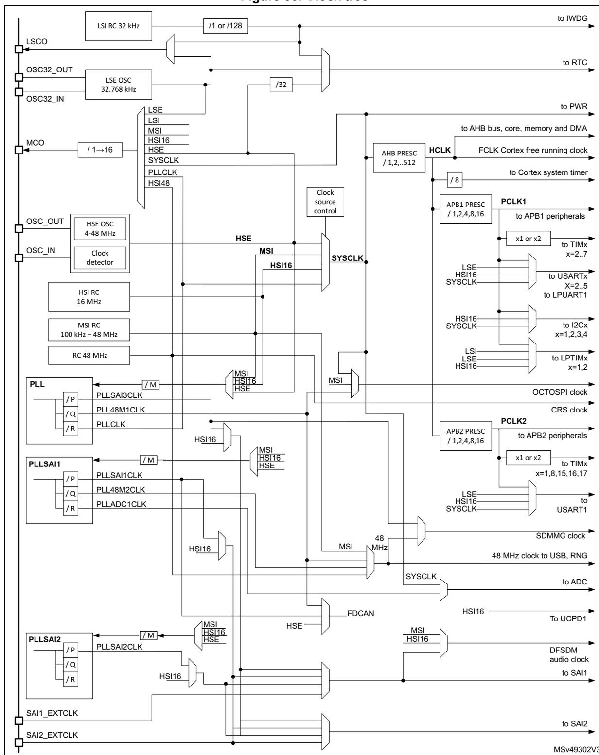
The diagram illustrates the internal clock tree of a microcontroller. On the left, various clock sources are shown:
- LSI RC 32 kHz : Connected to LSCO and IWDG via a /1 or /128 prescaler.
- LSE OSC 32.768 kHz : Connected to OSC32_IN, OSC32_OUT, RTC, and PWR.
- HSE OSC 4-48 MHz : Connected to OSC_IN, OSC_OUT, and a clock detector.
- Internal RC oscillators : HSI RC (16 MHz), MSI RC (100 kHz – 48 MHz), and RC 48 MHz.
- PLL : Configurable with /P, /Q, and /R dividers. Inputs include PLLSAI3CLK, PLL48M1CLK, and PLLCLK.
- PLLSAI1 : Configurable with /P, /Q, and /R dividers. Outputs include PLLSA1CLK, PLL48M2CLK, and PLLADC1CLK.
- PLLSAI2 : Configurable with /P, /Q, and /R dividers. Output is PLLSAI2CLK.
- External clocks : SAI1_EXTCLK and SAI2_EXTCLK.
- AHB PRES (/1,2,..512) to generate HCLK , which feeds the AHB bus, core, memory, DMA, and Cortex system timer (via /8).
- APB1 PRES (/1,2,4,8,16) to generate PCLK1 , which feeds APB1 peripherals, TIMx (via x1 or x2), USARTx, LPUART1, I2Cx, and LPTIMx.
- APB2 PRES (/1,2,4,8,16) to generate PCLK2 , which feeds APB2 peripherals, TIMx (via x1 or x2), USART1, SDMMC clock, 48 MHz clock to USB/RNG, and ADC (via SYSCLK).
- Other connections include HSI16 to UCPD1, DFSDM audio clock to SAI1, and MSV49302V3 output.
- 1. For full details about the internal and external clock source characteristics, refer to the Electrical characteristics section in the datasheet.
- 2. The ADC clock can be derived from the AHB clock of the ADC bus interface, divided by a programmable factor (1, 2 or 4). When the programmable factor is '1', the AHB prescaler must be equal to '1'.
9.3.1 HSE clock
The high-speed external clock signal (HSE) can be generated from two possible clock sources:
- • HSE external crystal/ceramic resonator
- • HSE user external clock
The resonator and the load capacitors have to be placed as close as possible to the oscillator pins in order to minimize output distortion and startup stabilization time. The loading capacitance values must be adjusted according to the selected oscillator.
Figure 31. HSE/ LSE clock sources
| Clock source | Hardware configuration |
|---|---|
| External clock | 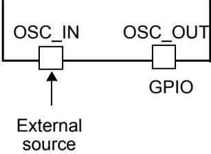 |
| Crystal/Ceramic resonators | 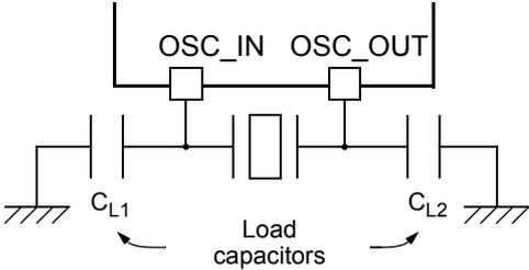 |
External crystal/ceramic resonator (HSE crystal)
The 4 to 48 MHz external oscillator has the advantage of producing a very accurate rate on the main clock.
The associated hardware configuration is shown in Figure 31 . Refer to the electrical characteristics section of the datasheet for more details.
The HSERDY flag in the RCC clock control register (RCC_CR) indicates if the HSE oscillator is stable or not. At startup, the clock is not released until this bit is set by hardware. An interrupt can be generated if enabled in the RCC clock interrupt enable register (RCC_CIER) .
The HSE crystal can be switched on and off using the HSEON bit in the RCC clock control register (RCC_CR) .
External source (HSE bypass)
In this mode, an external clock source must be provided. It can have a frequency of up to 48 MHz. This mode is selected by setting the HSEBYP and HSEON bits in the RCC clock control register (RCC_CR) . The external clock signal (square, sinus or triangle) with ~40-60 % duty cycle depending on the frequency (refer to the datasheet) must drive the OSC_IN pin while the OSC_OUT pin can be used a GPIO (see Figure 31 ).
9.3.2 HSI16 clock
The HSI16 clock signal is generated from an internal 16 MHz RC oscillator.
The HSI16 RC oscillator has the advantage of providing a clock source at low cost (no external components). It also has a faster startup time than the HSE crystal oscillator. However, even with calibration, the frequency is less accurate than an external crystal oscillator or ceramic resonator.
The HSI16 clock can be selected as system clock after wakeup from Stop modes (Stop 0, Stop 1 or Stop 2). Refer to Section 9.4: Low-power modes . It can also be used as a backup clock source (auxiliary clock) if the HSE crystal oscillator fails. Refer to Section 9.3.11: Clock security system (CSS) .
Calibration
The RC oscillator frequencies may vary from one chip to another due to manufacturing process variations, this is why each device is factory calibrated by ST for 1 % accuracy at \( T_A = 25^\circ\text{C} \) .
After reset, the factory calibration value is loaded in the HSICAL[7:0] bits in the RCC internal clock sources calibration register (RCC_ICSCR) .
If the application is subject to voltage or temperature variations this may affect the RC oscillator speed. The HSI16 frequency can be trimmed in the application using the HSITRIM[6:0] in the RCC internal clock sources calibration register (RCC_ICSCR) .
For more details on how to measure the HSI16 frequency variation, refer to Section 9.3.18: Internal/external clock measurement with TIM15/TIM16/TIM17 .
The HSIRDY flag in the RCC clock control register (RCC_CR) indicates if the HSI16 RC is stable or not. At startup, the HSI16 RC output clock is not released until this bit is set by hardware.
The HSI16 RC can be switched on and off using the HSION bit in the RCC clock control register (RCC_CR) .
The HSI16 signal can also be used as a backup source (Auxiliary clock) if the HSE crystal oscillator fails. Refer to Section 9.3.11: Clock security system (CSS) on page 335 .
9.3.3 MSI clock
The MSI clock signal is generated from an internal RC oscillator. Its frequency range can be adjusted by software by using the MSIRANGE[3:0] bits in the RCC clock control register (RCC_CR) . Twelve frequency ranges are available: 100 kHz, 200 kHz, 400 kHz, 800 kHz, 1 MHz, 2 MHz, 4 MHz (default value), 8 MHz, 16 MHz, 24 MHz, 32 MHz and 48 MHz.
The MSI clock is used as system clock after restart from Reset, wakeup from Standby and Shutdown low-power modes. After restart from Reset, the MSI frequency is set to its default value 4 MHz. Refer to Section 9.4: Low-power modes .
The MSI clock can be selected as system clock after a wakeup from Stop mode (Stop 0, Stop 1 or Stop 2). Refer to Section 9.4: Low-power modes . It can also be used as a backup clock source (auxiliary clock) if the HSE crystal oscillator fails. Refer to Section 9.3.11: Clock security system (CSS) .
The MSI RC oscillator has the advantage of providing a low-cost (no external components) low-power clock source. In addition, when used in PLL-mode with the LSE, it provides a very accurate clock source that can be used by the USB FS device, and feed the main PLL to run the system at the maximum speed 110 MHz.
The MSIRDY flag in the RCC clock control register (RCC_CR) indicates whether the MSI RC is stable or not. At startup, the MSI RC output clock is not released until this bit is set by hardware. The MSI RC can be switched on and off by using the HSION bit in the RCC clock control register (RCC_CR) .
Hardware auto calibration with LSE (PLL-mode)
When a 32.768 kHz external oscillator is present in the application, it is possible to configure the MSI in a PLL-mode by setting the MSIPLLEN bit in the RCC clock control register (RCC_CR) . When configured in PLL-mode, the MSI automatically calibrates itself thanks to the LSE. This mode is available for all MSI frequency ranges. At 48 MHz, the MSI in PLL-mode can be used for the USB FS device, saving the need of an external high-speed crystal.
Software calibration
The MSI RC oscillator frequency may vary from one chip to another due to manufacturing process variations, this is why each device is factory calibrated by ST for 1 % accuracy at an ambient temperature, \( T_A = 25\text{ }^\circ\text{C} \) . After reset, the factory calibration value is loaded in the MSICAL[7:0] bits in the RCC internal clock sources calibration register (RCC_ICSCR) . If the application is subject to voltage or temperature variations, this may affect the RC oscillator speed. You can trim the MSI frequency in the application by using the MSITRIM[7:0] bits in the RCC_ICSCR register. For more details on how to measure the MSI frequency variation please refer to Section 9.3.18: Internal/external clock measurement with TIM15/TIM16/TIM17 .
Note: Hardware auto calibration with LSE must not be used in conjunction with software calibration.
9.3.4 HSI48 clock
The HSI48 clock signal is generated from an internal 48 MHz RC oscillator and can be used directly for USB and for random number generator (RNG) as well as SDMMC.
The internal 48 MHz RC oscillator is mainly dedicated to provide a high-precision clock to the USB peripheral by means of a special clock recovery system (CRS) circuitry. The CRS can use the USB SOF signal, the LSE or an external signal to automatically and quickly adjust the oscillator frequency on-fly. It is disabled as soon as the system enters Stop or Standby mode. When the CRS is not used, the HSI48 RC oscillator runs on its default frequency which is subject to manufacturing process variations.
For more details on how to configure and use the CRS peripheral please refer to Section 10: Clock recovery system (CRS) .
The HSI48RDY flag in the RCC_CRRCR register indicates whether the HSI48 RC oscillator is stable or not. At startup, the HSI48 RC oscillator output clock is not released until this bit is set by hardware.
The HSI48 can be switched on and off using the HSI48ON bit in the RCC_CRRCR register.
9.3.5 PLL
The device embeds three PLLs: PLL, PLLSAI1 and PLLSAI2. Each PLL provides up to three independent outputs. The internal PLLs can be used to multiply the HSI16, HSE or MSI output clock frequency. The PLLs input frequency must be between 4 and 16 MHz. The selected clock source for each PLL is divided by a dedicated programmable factor PLLM, PLLSAI1M, PLLSAI2M, from 1 to 8 to provide a clock frequency in the requested input range. Refer to Figure 30: Clock tree , RCC PLL configuration register (RCC_PLLCFGR) , RCC PLLSAI1 configuration register (RCC_PLLSAI1CFGR) and RCC PLLSAI2 configuration register (RCC_PLLSAI2CFGR) .
The PLLs configuration (selection of the input clock and multiplication factor) must be done before enabling the PLL. Once the PLL is enabled, these parameters cannot be changed.
To modify the PLL configuration, proceed as follows:
- 1. Disable the PLL by clearing PLLON to 0 in RCC clock control register (RCC_CR) .
- 2. Wait until PLLRDY bit is cleared. The PLL is now fully stopped.
- 3. Change the desired parameter.
- 4. Enable the PLL again by setting PLLON bit to 1.
- 5. Enable the desired PLL outputs by configuring PLLPEN, PLLQEN, PLLREN bits in RCC PLL configuration register (RCC_PLLCFGR) .
An interrupt can be generated when the PLL is ready, if enabled in the RCC clock interrupt enable register (RCC_CIER) .
The same procedure is applied for changing the configuration of PLLSA1 or PLLSA2:
- 1. Disable the PLLSA1/PLLSA2 by clearing PLLSA1ON/PLLSA2ON to 0 in RCC clock control register (RCC_CR) .
- 2. Wait until PLLSA1RDY/PLLSA2RDY bit is cleared. The PLLSA1/PLLSA2 is now fully stopped.
- 3. Change the desired parameter.
- 4. Enable the PLLSA1/PLLSA2 again by setting PLLSA1ON/PLLSA2ON bit to 1.
- 5. Enable the desired PLL outputs by configuring PLLSA1PEN/PLLSA2PEN, PLLSA1QEN, PLLSA1REN bits in RCC PLLSA1 configuration register (RCC_PLLSA1CFGR) or RCC PLLSA2 configuration register (RCC_PLLSA2CFGR) .
The PLL output frequency must not exceed 110 MHz.
The enable bit of each PLL output clock (PLLPEN, PLLQEN, PLLREN, PLLSA1PEN, PLLSA1QEN, PLLSA1REN and PLLSA2PEN) can be modified at any time without stopping the corresponding PLL.
The PLLREN bit cannot be cleared if PLLCLK is used as system clock.
9.3.6 LSE clock
The LSE crystal is a 32.768 kHz low-speed external crystal or ceramic resonator. It has the advantage of providing a low-power but highly accurate clock source to the real-time clock peripheral (RTC) for clock/calendar or other timing functions.
The LSE crystal is switched on and off using the LSEON bit in RCC Backup domain control register (RCC_BDCR) . The crystal oscillator driving strength can be changed at runtime using the LSEDRV[1:0] bits in the RCC Backup domain control register (RCC_BDCR) to obtain the best compromise between robustness and short start-up time on one side and low-power-consumption on the other side. The LSE drive can be decreased to the lower drive capability (LSEDRV = 00) when the LSE is ON. However, once LSEDRV is selected, the drive capability can not be increased if LSEON = 1.
The LSERDY flag in the RCC Backup domain control register (RCC_BDCR) indicates whether the LSE crystal is stable or not. At startup, the LSE crystal output clock signal is not released until this bit is set by hardware. An interrupt can be generated if enabled in the RCC clock interrupt enable register (RCC_CIER) .
External source (LSE bypass)
In this mode, an external clock source must be provided. It can have a frequency of up to 1 MHz. This mode is selected by setting the LSEBYP and LSEON bits in the RCC AHB1 peripheral clocks enable in Sleep and Stop modes register (RCC_AHB1SMENR) . The external clock signal (square, sinus or triangle) with ~50 % duty cycle has to drive the OSC32_IN pin while the OSC32_OUT pin can be used as GPIO. See Figure 31 .
9.3.7 LSE system clock
The LSE system clock (LSESYS) is generated by RCC to:
- • a peripheral when source clock is the LSE as LPTIM, USART, LPUART, TIMER, CRS
- • the system in case of one of the LSCOSEL, MCO, MSI PLL mode or CSS on LSE functionality is enabled
By default the LSESYS clock is disabled. To enable the LSESYS clock, proceed as follows:
- 1. Wait the LSE clock is ready and set the LSEON and LSERDY bits in RCC Backup domain control register (RCC_BDCR) .
- 2. Set the LSESYSEN bit in RCC_BDCR.
- 3. Wait the LSESYSClock is ready and set the LSESYSRDY bit in RCC_BDCR.
9.3.8 LSI clock
The LSI RC acts as a low-power clock source that can be kept running in Stop and Standby mode for the independent watchdog (IWDG) and RTC. The clock frequency is either 32 kHz or 250 Hz depending on the LSIPRE bit in RCC control/status register (RCC_CSR) . When using the IWDG, only the 32 kHz LSI clock is selected and forced on. For more details, refer to the electrical characteristics section of the datasheet.
The LSI RC can be switched on and off using the LSION bit in the RCC control/status register (RCC_CSR) .
The LSI prescaler clock (LSIPRE bit in RCC_CSR) is only taken into account when the LSION bit is reset.
The LSIRDY flag in the RCC control/status register (RCC_CSR) indicates if the LSI oscillator is stable or not. At startup, the clock is not released until this bit is set by hardware. An interrupt can be generated if enabled in the RCC clock interrupt enable register (RCC_CIER) .
9.3.9 System clock (SYSCLK) selection
Four different clock sources can be used to drive the system clock (SYSCLK):
- • MSI oscillator
- • HS16 oscillator
- • HSE oscillator
- • PLL
The system clock maximum frequency is 110 MHz. After a system reset, the MSI oscillator, at 4 MHz, is selected as system clock. When a clock source is used directly or through the PLL as a system clock, it is not possible to stop it.
A switch from one clock source to another occurs only if the target clock source is ready (clock stable after startup delay or PLL locked). If a clock source that is not yet ready is selected, the switch occurs when the clock source becomes ready. Status bits in the RCC internal clock sources calibration register (RCC_ICSCR) indicate which clock(s) is (are) ready and which clock is currently used as a system clock.
Clock source switching conditions:
- • Switching from HSE or HSI or MSI to PLL with AHB frequency (HCLK) higher than 80 MHz
- • Switching from PLL with HCLK higher than 80 MHz to HSE or HSI or MSI
Transition state:
- • Set the AHB prescaler HPRE[3:0] bits in RCC_CFGR to divide the system frequency by 2.
- • Switch system clock to PLL.
- • Wait for at least 1 µs and then reconfigure AHB prescaler bits to the needed HCLK frequency.
9.3.10 Clock source frequency versus voltage scaling
Table 79 gives the different clock source frequencies depending on the product voltage range.
Table 79. Clock source frequency
| Product voltage range | Clock frequency | |||
|---|---|---|---|---|
| MSI | HSI16 | HSE | PLL/PLLSAI1/PLLSAI2 | |
| Range 0 | 48 MHz | 16 MHz | 48 MHz | 110 MHz |
| Range 1 | 48 MHz | 16 MHz | 48 MHz | 80 MHz |
| Range 2 | 24 MHz range | 16 MHz | 26 MHz | 26 MHz |
9.3.11 Clock security system (CSS)
CSS can be activated by software. In this case, the clock detector is enabled after the HSE oscillator startups delay, and disabled when this oscillator is stopped.
If a failure is detected on the HSE clock, the HSE oscillator is automatically disabled, a clock failure event is sent to the break input of the advanced-control timers (TIM1/TIM8 and TIM15/16/17) and an interrupt is generated to inform the software about the failure (clock security system interrupt CSSI), allowing the MCU to perform rescue operations. The CSSI is linked to the Cortex ® -M33 NMI (non-maskable interrupt) exception vector.
Note: Once the CSS is enabled and if the HSE clock fails, the CSSI occurs and a NMI is automatically generated. The NMI is executed indefinitely unless the CSSI pending bit is cleared. As a consequence, in the NMI ISR, the user must clear the CSSI by setting the CSSC bit in the RCC clock interrupt clear register (RCC_CICR) .
If the HSE oscillator is used directly or indirectly as the system clock (indirectly means: it is used as PLL input clock and the PLL clock is used as system clock), a detected failure causes a switch of the system clock to the MSI or the HSI16 oscillator depending on the STOPWUCK configuration in the RCC clock configuration register (RCC_CFGR) , and the disabling of the HSE oscillator. If the HSE clock (divided or not) is the clock entry of the PLL used as system clock when the failure occurs, the PLL is disabled too.
9.3.12 Clock security system on LSE
A clock security system on LSE can be activated by software writing the LSECSSON bit in the RCC Backup domain control register (RCC_BDCR) . This bit can be disabled only by a hardware reset or RTC software reset, or after a failure detection on LSE. LSECSSON must be written after LSE and LSI are enabled (LSEON and LSION enabled) and ready (LSERDY and LSIRDY set by hardware, LSIPRE disabled), and after the RTC clock has been selected by RTCSEL.
The CSS on LSE is working in all modes except VBAT. It is working also under system reset (excluding power-on reset). If a failure is detected on the external 32 kHz oscillator, the LSE clock is no longer supplied to the RTC but no hardware action is made to the registers. If the MSI was in PLL-mode, this mode is disabled.
The CSS on LSE failure is detected by a tamper event.
In Standby mode a wakeup is generated. In other modes a TAMP interrupt can be sent to wake up the software (see Table 320: TAMP interconnection and Section 42.5: TAMP interrupts ).
The software must then disable the LSECSSON bit, stop the defective 32 kHz oscillator (disabling LSEON), and change the RTC clock source (no clock or LSI or HSE, with RTCSEL), or take any required action to secure the application.
The frequency of LSE oscillator have to be higher than 30 kHz to avoid false positive CSS detection.
9.3.13 ADC clock
The ADC clock is derived from the system clock, or from the PLLSAI1 or the PLLSAI2 output. It can reach 110 MHz and can be divided by the following prescalers values: 1,2,4,6,8,10,12,16,32,64,128 or 256 by configuring the ADC1_CCR register. It is asynchronous to the AHB clock.
Alternatively, the ADC clock can be derived from the AHB clock of the ADC bus interface, divided by a programmable factor (1, 2 or 4). This programmable factor is configured using the CKMODE bit fields in the ADC123_CCR register.
If the programmed factor is 1, the AHB prescaler must be set to 1.
9.3.14 RTC clock
The RTCCLK clock source can be either the HSE / 32, LSE or LSI clock. It is selected by programming the RTCSEL[1:0] bits in the RCC Backup domain control register (RCC_BDCR) . This selection cannot be modified without resetting the Backup domain. The system must always be configured so as to get a PCLK frequency greater then or equal to the RTCCLK frequency for a proper operation of the RTC.
The LSE clock is in the Backup domain, whereas the HSE and LSI clocks are not. Consequently:
- • If LSE is selected as RTC clock, the RTC continues to work even if the \( V_{DD} \) supply is switched off, provided the \( V_{BAT} \) supply is maintained.
- • If LSI is selected as the RTC clock, the RTC state is not guaranteed if the \( V_{DD} \) supply is powered off.
- • If the HSE clock divided by a prescaler is used as the RTC clock, the RTC state is not guaranteed if the \( V_{DD} \) supply is powered off or if the internal voltage regulator is powered off (removing power from the \( V_{CORE} \) domain).
When the RTC clock is LSE or LSI, the RTC remains clocked and functional under system reset.
9.3.15 Timer clock
The timer clock frequencies are automatically defined by hardware.
There are two cases:
- • If the APB prescaler equals 1, the timer clock frequencies are set to the APB domain frequency.
- • Otherwise, they are set to twice ( \( \times 2 \) ) the APB domain frequency.
9.3.16 Watchdog clock
If the independent watchdog (IWDG) is started by either hardware option or software access, the LSI oscillator is forced on and cannot be disabled. After the LSI oscillator temporization, the LSI 32 kHz clock is provided to the IWDG.
9.3.17 Clock-out capability
- • MCO
The microcontroller clock output (MCO) capability allows the clock to be output onto the external MCO pin. One of eight clock signals can be selected as MCO clock.
- – LSI
- – LSE
- – SYSCLK
- – HSI16
- – HSI48
- – HSE
- – PLLCLK
- – MSI
The selection is controlled by the MCOSEL[3:0] bits of the RCC clock configuration register (RCC_CFGR) . The selected clock can be divided with the MCOPRE[2:0] field of the RCC clock configuration register (RCC_CFGR) .
- • LSCO
Another output (LSCO) allows one of the low-speed clocks below to be output onto the external LSCO pin:
- – LSI
- – LSE
This output remains available in Stop (Stop 0, Stop 1 and Stop 2) and Standby modes. The selection is controlled by the LSCOSEL bit and enabled with the LSCOEN in the RCC Backup domain control register (RCC_BDCR) .
The MCO clock output requires the corresponding alternate function selected on the MCO pin. The LSCO pin must be left in default POR state.
9.3.18 Internal/external clock measurement with TIM15/TIM16/TIM17
It is possible to indirectly measure the frequency of all on-board clock sources by mean of the TIM15, TIM16 or TIM17 channel 1 input capture, as represented Figure 32 , Figure 33 and Figure 34 .
Figure 32. Frequency measurement with TIM15 in capture mode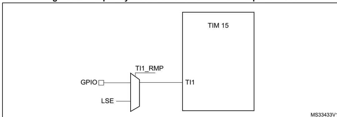
The diagram illustrates the connection for frequency measurement using TIM15. On the left, a multiplexer selects between two input signals: a GPIO and an LSE. The output of the multiplexer is connected to the TI1 input of a block labeled 'TIM 15'. Above the multiplexer, the label 'TI1_RMP' indicates the control signal for the selection. In the bottom right corner of the diagram area, the text 'MS33433V1' is present.
The input capture channel of the Timer 15 can be a GPIO line or an internal clock of the MCU. This selection is performed through the TI1_RMP bit in the TIM15_OR register. The possibilities are the following ones:
- • TIM15 Channel1 is connected to the GPIO. Refer to the alternate function mapping in the device datasheets.
- • TIM15 Channel1 is connected to the LSE.
![Figure 33: Frequency measurement with TIM16 in capture mode. The diagram shows a multiplexer selecting between a GPIO, LSI, LSE, and an RTC wakeup interrupt signal to connect to the TI1 input of a TIM16 block. The selection is controlled by the TI1_RMP[1:0] bits.](/RM0438-STM32L5/897fed17d1d7683da8748f7b7eb2759a_img.jpg)
The diagram illustrates the connection for frequency measurement using TIM16. On the left, a multiplexer selects between four input signals: a GPIO, LSI, LSE, and an RTC wakeup interrupt. The output of the multiplexer is connected to the TI1 input of a block labeled 'TIM16'. Above the multiplexer, the label 'TI1_RMP[1:0]' indicates the control signal for the selection. In the bottom right corner of the diagram area, the text 'MS33434V1' is present.
The input capture channel of the Timer 16 can be a GPIO line or an internal clock of the MCU. This selection is performed through the TI1_RMP[1:0] bits in the TIM16_OR register. The possibilities are the following ones:
- • TIM16 Channel1 is connected to the GPIO. Refer to the alternate function mapping in the device datasheets.
- • TIM16 Channel1 is connected to the LSI clock.
- • TIM16 Channel1 is connected to the LSE clock.
- • TIM16 Channel1 is connected to the RTC wakeup interrupt signal. In this case the RTC interrupt should be enabled.
Figure 34. Frequency measurement with TIM17 in capture mode
![Diagram showing the connection of TIM17 Channel 1 (TI1) to various clock sources. On the left, a multiplexer selects between GPIO, MSI, HSE/32, and MCO. The output of the multiplexer is connected to the TI1 input of the TIM17 block. The selection is controlled by the TI1_RMP[1:0] bits. The diagram is labeled MS33435V1.](/RM0438-STM32L5/6b89ce8be0091cec81aaaad513a8b93f_img.jpg)
The diagram illustrates the internal architecture for connecting the TIM17 timer's input capture channel 1 (TI1) to different clock sources. A multiplexer (MUX) is shown on the left, with four inputs: GPIO, MSI, HSE/32, and MCO. The output of this MUX is connected to the TI1 pin of the TIM17 block. Above the MUX, the control signals for the selection are labeled TI1_RMP[1:0]. The TIM17 block is represented by a rectangle on the right. In the bottom right corner of the diagram area, the text 'MS33435V1' is present.
The input capture channel of the Timer 17 can be a GPIO line or an internal clock of the MCU. This selection is performed through the TI1_RMP[1:0] bits in the TIM17_OR register. The possibilities are the following ones:
- • TIM17 Channel1 is connected to the GPIO. Refer to the alternate function mapping in the device datasheets.
- • TIM17 Channel1 is connected to the MSI Clock.
- • TIM17 Channel1 is connected to the HSE/32 Clock.
- • TIM17 Channel1 is connected to the microcontroller clock output (MCO), this selection is controlled by the MCOSEL[3:0] bits of the RCC_CFGR register.
Calibration of the HSI16 and the MSI
For TIM15 and TIM16, the primary purpose of connecting the LSE to the channel 1 input capture is to be able to precisely measure the HSI16 and MSI system clocks (for this, either HSI16 or MSI must be used as system clock source). The number of HSI16 (MSI, respectively) clock counts between consecutive edges of the LSE signal provides a measure of the internal clock period. Taking advantage of the high precision of LSE crystals (typically a few tens of ppm), it is possible to determine the internal clock frequency with the same resolution, and trim the source to compensate manufacturing, process, temperature and/or voltage related frequency deviations.
The MSI and HSI16 oscillator both have dedicated user-accessible calibration bits for this purpose.
The basic concept consists in providing a relative measurement (such as the HSI16/LSE ratio). The precision is therefore closely related to the ratio between the two clock sources. The higher the ratio is, the better the measurement is. If LSE is not available, HSE/32 is the better option in order to reach the most precise calibration possible.
It is however not possible to have a good enough resolution when the MSI clock is low (typically below 1 MHz). In this case, the following steps are needed:
- 1. Accumulate the results of several captures in a row.
- 2. Use the timer input capture prescaler (up to 1 capture every 8 periods).
- 3. Use the RTC wakeup interrupt signal (when the RTC is clocked by the LSE) as the input for the channel1 input capture. This improves the measurement precision. For this purpose the RTC wakeup interrupt must be enabled.
Calibration of the LSI
The calibration of the LSI follows the same pattern that for the HSI16, but changing the reference clock. It is necessary to connect LSI clock to the channel 1 input capture of the TIM16. Then defining the HSE as system clock source, the number of its clock counts between consecutive edges of the LSI signal provides a measure of the internal low-speed clock period.
The basic concept consists in providing a relative measurement (such as the HSE/LSI ratio). The precision is therefore closely related to the ratio between the two clock sources. The higher the ratio is, the better the measurement is.
9.3.19 Peripheral clock enable registers (RCC_AHBxENR, RCC_APBxENRy)
Each peripheral clock can be enabled by the corresponding EN bit in the RCC_AHBxENR and RCC_APBxENRy registers.
When the peripheral clock is not active, read or write accesses to the peripheral registers are not supported.
The enable bit has a synchronization mechanism to create a glitch-free clock for the peripheral. After the enable bit is set, there is a 2-clock-cycles delay before the clock is active.
Caution: Just after enabling the clock for a peripheral, the software must wait for a delay before accessing the peripheral registers.
9.4 Low-power modes
- • AHB and APB peripheral clocks, including DMA clock, can be disabled by software.
- • Sleep and Low-power sleep modes stop the CPU clock. The memory interface clocks (flash memory, SRAM1 and SRAM2 interfaces) can be stopped by software during Sleep mode. The AHB to APB bridge clocks are disabled by hardware during Sleep mode when all the clocks of the peripherals connected to them are disabled.
- • Stop modes (Stop 0, Stop 1 and Stop 2) stop all the clocks in the \( V_{CORE} \) domain and disable the three PLL, HSI16, MSI and HSE oscillators.
All U(S)ARTs, LPUARTs and I2Cs have the capability to enable the HSI16 oscillator even when the MCU is in Stop mode (if HSI16 is selected as the clock source for that peripheral).
All U(S)ARTs and LPUARTs can also be driven by the LSE oscillator when the system is in Stop mode (if LSE is selected as clock source for that peripheral) and the LSE oscillator is enabled (LSEON). In that case the LSE remains always ON in Stop mode (no capability to turn on the LSE oscillator).
- • Standby and Shutdown modes stop all the clocks in the \( V_{CORE} \) domain and disable the PLLs, HSI16, MSI and HSE oscillators.
The CPU's deepsleep mode can be overridden for debugging by setting the DBG_STOP or DBG_STANDBY bits in the DBGMCU_CR register.
When exiting Stop modes (Stop 0, Stop 1 or Stop 2), the system clock is either MSI or HSI16, depending on the software configuration of the STOPWUCK bit in the RCC_CFGR register. The frequency (range and user trim) of the MSI oscillator is the one configured
before entering Stop mode. The user trim of HSI16 is kept. If the MSI was in PLL-mode before entering Stop mode, the PLL-mode stabilization time must be waited for after wakeup even if the LSE was kept ON during the Stop mode.
When leaving the Standby and Shutdown modes, the system clock is MSI. The MSI frequency at wakeup from Standby mode is configured with the MSISRANGE in the RCC_CSR register, from 1 to 8 MHz. The MSI frequency at wakeup from Shutdown mode is 4 MHz. The user trim is lost.
If a flash memory programming operation is on going, Stop, Standby and Shutdown modes entry is delayed until the flash memory interface access is finished. If an access to the APB domain is ongoing, Stop, Standby and Shutdown modes entry is delayed until the APB access is finished.
9.5 RCC TrustZone ® security
When the TrustZone security is activated by the TZEN option bit in the FLASH_OPTR register, the RCC is able to secure RCC configuration and status bits from being modified by non-secure accesses.
This is configured through the security configuration register RCC_SECCFGR to prevent non-secure access to read or modify the following features:
- • HSE, HSE-CSS, HSI, MSI, LSI, LSE, LSE-CSS, HSI48 configuration and status bits
- • main PLL, PLLSAI1, PLLSAI2, AHB prescaler configuration and status bits
- • system clock SYSCLK and HSI48 source clock selection and status bits
- • MCO clock output configuration and STOPWUCK bit
- • reset flag RMVF configuration
When a peripheral is configured as secure, its related clock, reset, clock source selection and clock enable during low-power modes control bits are also secure in the RCC_AHBxENR, RCC_APBxENR, RCC_AHBxSMEN, RCC_APBxSMEN, RCC_CCIPR1 and RCC_CCIPR2 registers.
A peripheral is secure when:
- • For securable peripherals by TZSC (TrustZone security controller), the SEC security bit corresponding to this peripheral is set in the TZSC_SECCFGRx register.
- • For TrustZone-aware peripherals, a security feature of this peripheral is enabled through its dedicated bits.
Table 80 gives a summary of the RCC secured bits following the security configuration bit in the RCC_SECCFGR register.
When one security configuration bit is set, some configuration and status bits are secured. The RCC registers may contain secure and non-secure bits:
- • Secured bits: read and write operations are only allowed by a secure access. Non-secure read or write accesses are RAZ/WI. There is no illegal access event generated.
- • Non-secure bits: no restriction. Read and write operations are allowed by both secure and non-secure accesses.
- • A non-secure read/write access to RCC_SECCFGR register is RAZ/WI and generates an illegal access event. An illegal access interrupt is generated if the RCC illegal access interrupt is enabled in the TZIC_IER2 register.
When the TrustZone security is disabled (TZEN = 0 in FLASH_OPTR register), all registers are non-secure. The RCC_SECCFGR secure register and security status registers are RAZ/WI.
Table 80. RCC security configuration summary
| Configuration bit in RCC_SECCFGR | Secured bits | Corresponding register |
|---|---|---|
| HSISEC | HSION, HSIKERON, HSIRDY, HSIASFS | RCC_CR |
| HSICAL[7:0], HSITRIM[6:0] | RCC_ICSCR | |
| HSIRDYIE | RCC_CIER | |
| HSIRDYC | RCC_CICR | |
| HSESEC | HSEON, HSERDY, HSEBYP, HSECSSON | RCC_CR |
| HSERDYIE | RCC_CIER | |
| HSERDYC, HSECSSC | RCC_CICR | |
| MSISEC | MSION, MSIRDY, MSIPLLEN, MSIRGSEL, MSISRANGE[3:0] | RCC_CR |
| MSICAL[7:0], MSITRIM[7:0] | RCC_ICSCR | |
| MISRANGE[3:0] | RCC_CSR | |
| MSIRDYIE | RCC_CIER | |
| LSISEC | LSIO, LSIRDY, LSIPRE | RCC_CSR |
| LSIRDYIE | RCC_CIER | |
| LSIRDYC | RCC_CICR | |
| LSESEC | LSECSSON, LSECSSD, LSEDRV[1:0], LSEBYP, LSERDY, LSEON, LSCOSEL, LSCOEN | RCC_BDCR |
| LSERDYIE, LSECSSIE | RCC_CIER | |
| LSERDYC, LSECSSC | RCC_CICR | |
| SYSCLKSEC | SW[1:0], SWS[1:0], STOPWUCK, MCOSEL[3:0], MCOPRE[2:0], | RCC_CFGR |
| VOS[1:0] | PWR_CR1 | |
| PRESCSEC | HPRE[3:0], PPRE1[2:0], PPRE2[2:0] | RCC_CFGR |
| PLLSEC | PLLSRC[1:0], PLLM[3:0], PLLN[6:0], PLLPDIV[4:0], PLLR[1:0], PLLREN, PLLQ[1:0], PLLP, PLLPEN, PLLQEN | RCC_PLLCFGR |
| PLL RDY, PLLON | RCC_CR | |
| PLL RDYIE | RCC_CIER | |
| PLL RDYC | RCC_CICR | |
| PLLSAI1SEC | PLLSAI1PDIV[4:0], PLLSAI1R[1:0], PLLSAI1REN, PLLSAI1Q[1:0], PLLSAI1QEN, PLLSAI1P, PLLSAI1PEN, PLLSAI1N[6:0], PLLSAI1M[3:0], PLLSAI1SRC[1:0] | RCC_PLLSAI1CFGR |
| PLLSAI1RDY, PLLSAI1ON | RCC_CR | |
| PLLSAI1RDYIE | RCC_CIER | |
| PLLSAI1RDYC | RCC_CICR |
Table 80. RCC security configuration summary (continued)
| Configuration bit in RCC_SECCFGR | Secured bits | Corresponding register |
|---|---|---|
| PLL2SEC | PLL2PDIV[4:0], PLL2P, PLL2PEN, PLL2N[6:0], PLL2M[3:0], PLL2SRC[1:0] | RCC_PLL2CFGR |
| PLL2RDY, PLL2ON | RCC_CR | |
| PLL2RDYIE | RCC_CIER | |
| PLL2RDYC | RCC_CICR | |
| HSI48SEC | HSI48CAL[8:0], HSI48RDY | RCC_CRRCR |
| HSI48RDYE | RCC_CIER | |
| HSI48RDYC | RCC_CICR | |
| CLK48MSEC | CLK48MSEL[1:0] | RCC_CCIPR1 |
| RMVFSEC | RMVF | RCC_CSR |
9.6 RCC Privileged and Unprivileged mode
By default, after reset, all RCC registers can be read or written in both Privileged and Unprivileged modes except RCC privilege bit (PRIV bit in RCC_CR) that can be written in Privileged mode only.
When the PRIV bit is set in RCC_CR register:
- • Writing the RCC registers is possible only in privileged mode.
- • All RCC registers can be read only in privileged mode except RCC security status registers (RCC_AHBxSECSR, RCC_APBx_SECSR, RCC_SECSR) and PRIV bit in RCC_CR register.
- • An unprivileged access to a privileged RCC register is discarded. RAZ/WI.
9.7 RCC interrupts
The RCC provides three interrupt lines:
- • rcc_it : general interrupt line providing events when the PLLs are ready or when the oscillators are ready
- • rcc_hsecss_it : interrupt line dedicated to the failure detection of the HSE CSS (clock security system)
- • rcc_lsecss_it : interrupt line dedicated to the failure detection of the LSE CSS
The interrupt enable is controlled via RCC clock interrupt enable register (RCC_CIER) , except for the HSE CSS failure. When the HSE CSS feature is enabled, it is not possible to mask the interrupt generation.
The interrupt flags can be checked via RCC clock interrupt flag register (RCC_CIFR) , and those flags can be cleared via RCC clock interrupt clear register (RCC_CICR) .
Note: The interrupt flags are not relevant if the corresponding interrupt enable bit is not set.
Table 81 gives a summary of the interrupt sources and the way to control them.
Table 81. Interrupt sources and control (1)| Interrupt vector | Interrupt event flag | Description | Enable control bit | Interrupt clear method | Interrupt internal signal |
|---|---|---|---|---|---|
| RCC RCC_S | LSIRDYF | LSI ready | LSIRDYIE | Set LSIRDYC to 1 | rcc_it |
| LSERDYF | LSE ready | LSERDYIE | Set LSERDYC to 1 | ||
| HSIDRYF | HSI ready | HSIDRYIE | Set HSIRDYC to 1 | ||
| HSERDYF | HSE ready | HSERDYIE | Set HSERDYC to 1 | ||
| CSIRDYF | CSI ready | CSIRDYIE | Set CSIRDYC to 1 | ||
| HSI48RDYF | HSI48 ready | HSI48RDYIE | Set HSI48RDYC to 1 | ||
| PLLRDYF | PLL ready | PLLRDYIE | Set PLLRDYC to 1 | ||
| PLLSAI1RDYF | PLLSAI1 ready | PLLSAI1RDYIE | Set PLLSAI1RDYC to 1 | ||
| PLLSAI2RDYF | PLLSAI2 ready | PLLSAI2RDYIE | Set PLLSAI2RDYC to 1 | ||
| TAMP TAMP_S | ITAMP3F | LSE CSS failure | ITAMP3IE (2) | Set CITAMP3F to 1 | rcc_lsecss_it |
| NMI | HSECSSF | HSE CSS failure | _(3) | Set HSECSSC to 1 | rcc_hsecss_it |
1. When TrustZone is enabled, two interrupt vectors are available for secure and non-secure events.
2. The security system feature must also be enabled (LSECSSON = 1), in order to generate interrupts.
3. It is not possible to mask this interrupt when the security system feature is enabled (HSECSSON = 1).
9.8 RCC registers
9.8.1 RCC clock control register (RCC_CR)
Address offset: 0x000
Reset value: 0x0000 0063
HSEBYP is cleared upon power-on reset. It is not affected upon other types of reset.
Access: no wait state, word, half-word and byte access
| 31 | 30 | 29 | 28 | 27 | 26 | 25 | 24 | 23 | 22 | 21 | 20 | 19 | 18 | 17 | 16 |
|---|---|---|---|---|---|---|---|---|---|---|---|---|---|---|---|
| PRIV | Res. | PLLSAI2RDY | PLLSAI2ON | PLLSAI1RDY | PLLSAI1ON | PLLRDY | PLLON | Res. | Res. | Res. | Res. | CSSON | HSEBYP | HSERDY | HSEON |
| 15 | 14 | 13 | 12 | 11 | 10 | 9 | 8 | 7 | 6 | 5 | 4 | 3 | 2 | 1 | 0 |
| Res. | Res. | Res. | Res. | HSIASFS | HSIRDY | HSIKERON | HSION | MSIRANGE[3:0] | MSIRGSEL | MSIPLLEN | MSIRDY | MSION | |||
| rw | r | rw | rw | rw | rw | rw | rw | rs | rw | r | rw | ||||
Bit 31 PRIV: RCC privilege
Set and reset by software. This bit can be read by both privileged or unprivileged access. When set, it can only be cleared by a privileged access.
0: RCC registers can be accessed by a privileged or non-privileged access.
1: RCC registers can be accessed only by a privileged access except RCC_AHBxSECSR, RCC_APBx_SECSR and RCC_SECSR.
An unprivileged access to RCC registers is RAZ/WI.
If TrustZone security is enabled (TZEN = 1), when the RCC is not secure, the PRIV bit can be written by a secure or non-secure privileged access.
If the RCC is secure, the PRIV bit can be written only by a secure privileged access. A non-secure write access is ignored.
A secure unprivileged write access on PRIV bit is ignored.
Bit 30 Reserved, must be kept at reset value.
Bit 29 PLLSAI2RDY: SAI2 PLL clock ready flag
Set by hardware to indicate that the PLLSAI2 is locked.
0: PLLSAI2 unlocked
1: PLLSAI2 locked
Bit 28 PLLSAI2ON: SAI2 PLL enable
Set and cleared by software to enable PLLSAI2.
Cleared by hardware when entering Stop, Standby or Shutdown mode.
0: PLLSAI2 OFF
1: PLLSAI2 ON
Bit 27 PLLSAI1RDY: SAI1 PLL clock ready flag
Set by hardware to indicate that the PLLSAI1 is locked.
0: PLLSAI1 unlocked
1: PLLSAI1 locked
Bit 26 PLLSAI1ON : SAI1 PLL enable
Set and cleared by software to enable PLLSAI1.
Cleared by hardware when entering Stop, Standby or Shutdown mode.
0: PLLSAI1 OFF
1: PLLSAI1 ON
Bit 25 PLLRDY : main PLL clock ready flag
Set by hardware to indicate that the main PLL is locked.
0: PLL unlocked
1: PLL locked
Bit 24 PLLON : main PLL enable
Set and cleared by software to enable the main PLL.
Cleared by hardware when entering Stop, Standby or Shutdown mode. This bit cannot be reset if the PLL clock is used as the system clock.
0: PLL OFF
1: PLL ON
Bits 23:20 Reserved, must be kept at reset value.
Bit 19 CSSON : clock security system enable
Set by software to enable the clock security system. When CSSON is set, the clock detector is enabled by hardware when the HSE oscillator is ready, and disabled by hardware if a HSE clock failure is detected. This bit is set only and is cleared by reset.
0: clock security system OFF (clock detector OFF)
1: clock security system ON (clock detector ON if the HSE oscillator is stable, OFF if not).
Bit 18 HSEBYP : HSE crystal oscillator bypass
Set and cleared by software to bypass the oscillator with an external clock. The external clock must be enabled with the HSEON bit set, to be used by the device. The HSEBYP bit can be written only if the HSE oscillator is disabled.
0: HSE crystal oscillator not bypassed
1: HSE crystal oscillator bypassed with external clock
Bit 17 HSERDY : HSE clock ready flag
Set by hardware to indicate that the HSE oscillator is stable.
0: HSE oscillator not ready
1: HSE oscillator ready
Note: Once the HSEON bit is cleared, HSERDY goes low after 6 HSE clock cycles.
Bit 16 HSEON : HSE clock enable
Set and cleared by software.
Cleared by hardware to stop the HSE oscillator when entering Stop, Standby or Shutdown mode. This bit cannot be reset if the HSE oscillator is used directly or indirectly as the system clock.
0: HSE oscillator OFF
1: HSE oscillator ON
Bits 15:12 Reserved, must be kept at reset value.
Bit 11 HSIASFS : HSI16 automatic start from Stop
Set and cleared by software. When the system wakeup clock is MSI, this bit is used to wakeup the HSI16 is parallel of the system wakeup.
0: HSI16 oscillator is not enabled by hardware when exiting Stop mode with MSI as wakeup clock.
1: HSI16 oscillator is enabled by hardware when exiting Stop mode with MSI as wakeup clock.
Bit 10 HSIRDY : HSI16 clock ready flag
Set by hardware to indicate that HSI16 oscillator is stable. This bit is set only when HSI16 is enabled by software by setting HSION.
0: HSI16 oscillator not ready
1: HSI16 oscillator ready
Note: Once the HSION bit is cleared, HSIRDY goes low after 6 HSI16 clock cycles.
Bit 9 HSIKERON : HSI16 always enable for peripheral kernels.
Set and cleared by software to force HSI16 ON even in Stop modes. The HSI16 can only feed USARTs and I 2 Cs peripherals configured with HSI16 as kernel clock. Keeping the HSI16 ON in Stop mode allows to avoid slowing down the communication speed because of the HSI16 startup time. This bit has no effect on HSION value.
0: No effect on HSI16 oscillator.
1: HSI16 oscillator is forced ON even in Stop mode.
Bit 8 HSION : HSI16 clock enable
Set and cleared by software.
Cleared by hardware to stop the HSI16 oscillator when entering Stop, Standby or Shutdown mode.
Set by hardware to force the HSI16 oscillator ON when STOPWUCK=1 or HSICASFS = 1 when leaving Stop modes, or in case of failure of the HSE crystal oscillator.
This bit is set by hardware if the HSI16 is used directly or indirectly as system clock.
0: HSI16 oscillator OFF
1: HSI16 oscillator ON
Bits 7:4 MSIRANGE[3:0] : MSI clock ranges
These bits are configured by software to choose the frequency range of MSI when MSIRGSEL is set. 12 frequency ranges are available:
0000: range 0 around 100 kHz
0001: range 1 around 200 kHz
0010: range 2 around 400 kHz
0011: range 3 around 800 kHz
0100: range 4 around 1M Hz
0101: range 5 around 2 MHz
0110: range 6 around 4 MHz (reset value)
0111: range 7 around 8 MHz
1000: range 8 around 16 MHz
1001: range 9 around 24 MHz
1010: range 10 around 32 MHz
1011: range 11 around 48 MHz
others: not allowed (hardware write protection)
Note: Warning: MSIRANGE can be modified when MSI is OFF (MSION=0) or when MSI is ready (MSIRDY=1). MSIRANGE must NOT be modified when MSI is ON and NOT ready (MSION=1 and MSIRDY=0)
Bit 3 MSIRGSEL : MSI clock range selection
Set by software to select the MSI clock range with MSIRANGE[3:0]. Write 0 has no effect. After a standby or a reset MSIRGSEL is at 0 and the MSI range value is provided by MSISRANGE in CSR register.
0: MSI Range is provided by MSISRANGE[3:0] in RCC_CSR register
1: MSI Range is provided by MSIRANGE[3:0] in the RCC_CR register
Bit 2 MSIPLLEN : MSI clock PLL enableSet and cleared by software to enable/ disable the PLL part of the MSI clock source.
MSIPLLEN must be enabled after LSE is enabled (LSEON enabled) and ready (LSERDY set by hardware). There is a hardware protection to avoid enabling MSIPLLEN if LSE is not ready.
This bit is cleared by hardware when LSE is disabled (LSEON = 0) or when the Clock Security System on LSE detects a LSE failure (refer to RCC_CSR register).
0: MSI PLL OFF
1: MSI PLL ON
Bit 1 MSIRDY : MSI clock ready flagThis bit is set by hardware to indicate that the MSI oscillator is stable.
0: MSI oscillator not ready
1: MSI oscillator ready
Note: Once the MSION bit is cleared, MSIRDY goes low after 6 MSI clock cycles.
Bit 0 MSION : MSI clock enableThis bit is set and cleared by software.
Cleared by hardware to stop the MSI oscillator when entering Stop, Standby or Shutdown mode.
Set by hardware to force the MSI oscillator ON when exiting Standby or Shutdown mode.
Set by hardware to force the MSI oscillator ON when STOPWUCK=0 when exiting from Stop modes, or in case of a failure of the HSE oscillator
Set by hardware when used directly or indirectly as system clock.
0: MSI oscillator OFF
1: MSI oscillator ON
9.8.2 RCC internal clock sources calibration register (RCC_ICSCR)
Address offset: 0x004
Reset value: 0x40XX 00XX
X is factory-programmed.
Access: no wait state, word, half-word and byte access
| 31 | 30 | 29 | 28 | 27 | 26 | 25 | 24 | 23 | 22 | 21 | 20 | 19 | 18 | 17 | 16 |
|---|---|---|---|---|---|---|---|---|---|---|---|---|---|---|---|
| Res. | HSITRIM[6:0] | HSICAL[7:0] | |||||||||||||
| rw | rw | rw | rw | rw | rw | rw | r | r | r | r | r | r | r | r | |
| 15 | 14 | 13 | 12 | 11 | 10 | 9 | 8 | 7 | 6 | 5 | 4 | 3 | 2 | 1 | 0 |
| MSITRIM[7:0] | MSICAL[7:0] | ||||||||||||||
| rw | rw | rw | rw | rw | rw | rw | rw | r | r | r | r | r | r | r | r |
Bit 31 Reserved, must be kept at reset value.
Bits 30:24 HSITRIM[6:0] : HSI16 clock trimming
These bits provide an additional user-programmable trimming value that is added to the HSICAL[7:0] bits. It can be programmed to adjust to variations in voltage and temperature that influence the frequency of the HSI16.
Bits 23:16 HSICAL[7:0] : HSI16 clock calibration
These bits are initialized at startup with the factory-programmed HSI16 calibration trim value. When HSITRIM is written, HSICAL is updated with the sum of HSITRIM and the factory trim value.
Bits 15:8 MSITRIM[7:0] : MSI clock trimming
These bits provide an additional user-programmable trimming value that is added to the MSICAL[7:0] bits. It can be programmed to adjust to variations in voltage and temperature that influence the frequency of the MSI.
Bits 7:0 MSICAL[7:0] : MSI clock calibration
These bits are initialized at startup with the factory-programmed MSI calibration trim value. When MSITRIM is written, MSICAL is updated with the sum of MSITRIM and the factory trim value.
9.8.3 RCC clock configuration register (RCC_CFGR)
Address offset: 0x008
Reset value: 0x0000 0000
Access: \( 0 \le \text{wait state} \le 2 \) , word, half-word and byte access
1 or 2 wait states are inserted only if the access occurs during clock source switch.
From 0 to 15 wait states are inserted if the access occurs when the APB or AHB prescalers values update is on going.
| 31 | 30 | 29 | 28 | 27 | 26 | 25 | 24 | 23 | 22 | 21 | 20 | 19 | 18 | 17 | 16 |
|---|---|---|---|---|---|---|---|---|---|---|---|---|---|---|---|
| Res. | MCOPRE[2:0] | MCOSEL[3:0] | Res. | Res. | Res. | Res. | Res. | Res. | Res. | Res. | |||||
| rw | rw | rw | rw | rw | rw | rw | |||||||||
| 15 | 14 | 13 | 12 | 11 | 10 | 9 | 8 | 7 | 6 | 5 | 4 | 3 | 2 | 1 | 0 |
| STOPWUCK | Res. | PPRE2[2:0] | PPRE1[2:0] | HPRE[3:0] | SWS[1:0] | SW[1:0] | |||||||||
| rw | rw | rw | rw | rw | rw | rw | rw | rw | rw | rw | r | r | rw | rw | |
Bit 31 Reserved, must be kept at reset value.
Bits 30:28 MCOPRE[2:0] : microcontroller clock output prescaler
These bits are set and cleared by software.
It is highly recommended to change this prescaler before MCO output is enabled.
000: MCO divided by 1
001: MCO divided by 2
010: MCO divided by 4
011: MCO divided by 8
100: MCO divided by 16
Others: not allowed
Bits 27:24 MCOSEL[3:0] : microcontroller clock output
Set and cleared by software.
0000: MCO output disabled, no clock on MCO
0001: SYSCLK system clock selected
0010: MSI clock selected
0011: HSI16 clock selected
0100: HSE clock selected
0101: Main PLL clock selected
0110: LSI clock selected
0111: LSE clock selected
1000: Internal HSI48 clock selected
Others: reserved
Note: This clock output may have some truncated cycles at startup or during MCO clock source switching.
Bits 23:16 Reserved, must be kept at reset value.
Bit 15 STOPWUCK : wakeup from Stop and CSS backup clock selection
Set and cleared by software to select the system clock used when exiting Stop mode.
The selected clock is also used as emergency clock for the clock security system on HSE.
Warning: STOPWUCK must not be modified when the CSS is enabled by HSECSSON bit in the RCC_CR register and the system clock is HSE (SWS="10") or a switch on HSE is requested (SW="10").
0: MSI oscillator selected as wakeup from stop clock and CSS backup clock
1: HSI16 oscillator selected as wakeup from stop clock and CSS backup clock
Bit 14 Reserved, must be kept at reset value.
Bits 13:11 PPRE2[2:0] : APB high-speed prescaler (APB2)
Set and cleared by software to control the division factor of the APB2 clock (PCLK2).
0xx: HCLK not divided
100: HCLK divided by 2
101: HCLK divided by 4
110: HCLK divided by 8
111: HCLK divided by 16
Bits 10:8 PPRE1[2:0] : APB low-speed prescaler (APB1)
Set and cleared by software to control the division factor of the APB1 clock (PCLK1).
0xx: HCLK not divided
100: HCLK divided by 2
101: HCLK divided by 4
110: HCLK divided by 8
111: HCLK divided by 16
Bits 7:4 HPRE[3:0] : AHB prescaler
Set and cleared by software to control the division factor of the AHB clock.
Caution: Depending on the device voltage range, the software must set correctly these bits to ensure that the system frequency does not exceed the maximum allowed frequency (for more details, refer to Section 8.2.5: Dynamic voltage scaling management ). After a write operation to these bits and before decreasing the voltage range, this register must be read to be sure that the new value has been taken into account.
0xxx: SYSCLK not divided
1000: SYSCLK divided by 2
1001: SYSCLK divided by 4
1010: SYSCLK divided by 8
1011: SYSCLK divided by 16
1100: SYSCLK divided by 64
1101: SYSCLK divided by 128
1110: SYSCLK divided by 256
1111: SYSCLK divided by 512
Bits 3:2 SWS[1:0] : system clock switch status
Set and cleared by hardware to indicate which clock source is used as system clock.
00: MSI oscillator used as system clock
01: HSI16 oscillator used as system clock
10: HSE used as system clock
11: PLL used as system clock
Bits 1:0 SW[1:0] : system clock switch
Set and cleared by software to select system clock source (SYSCLK).
Configured by hardware to force MSI oscillator selection when exiting Standby or Shutdown mode. Configured by hardware to force MSI or HSI16 oscillator selection when exiting Stop mode or in case of failure of the HSE oscillator, depending on STOPWUCK value.
00: MSI selected as system clock
01: HSI16 selected as system clock
10: HSE selected as system clock
11: PLL selected as system clock
9.8.4 RCC PLL configuration register (RCC_PLLCFGR)
Address offset: 0x00C
Reset value: 0x0000 1000
Access: no wait state, word, half-word and byte access
This register is used to configure the PLL clock outputs according to the formulas:
- • \( f(\text{VCO clock}) = f(\text{PLL clock input}) \times (\text{PLLN} / \text{PLLM}) \)
- • \( f(\text{PLL\_P}) = f(\text{VCO clock}) / \text{PLLP} \)
- • \( f(\text{PLL\_Q}) = f(\text{VCO clock}) / \text{PLLQ} \)
- • \( f(\text{PLL\_R}) = f(\text{VCO clock}) / \text{PLLR} \)
| 31 | 30 | 29 | 28 | 27 | 26 | 25 | 24 | 23 | 22 | 21 | 20 | 19 | 18 | 17 | 16 |
|---|---|---|---|---|---|---|---|---|---|---|---|---|---|---|---|
| PLLPDIV[4:0] | PLLR[1:0] | PLLREN | Res. | PLLQ[1:0] | PLLQEN | Res. | Res. | PLLP | PLLREN | ||||||
| rw | rw | rw | rw | rw | rw | rw | rw | rw | rw | rw | rw | rw | |||
| 15 | 14 | 13 | 12 | 11 | 10 | 9 | 8 | 7 | 6 | 5 | 4 | 3 | 2 | 1 | 0 |
| Res. | PLLN[6:0] | PLLM[3:0] | Res. | Res. | PLL SRC[1:0] | ||||||||||
| rw | rw | rw | rw | rw | rw | rw | rw | rw | rw | rw | rw | rw | |||
Bits 31:27 PLLPDIV[4:0] : Main PLL division factor for PLLSAI3CLK
Set and cleared by software to control the SAI1 or SAI2 clock frequency.
PLLSAI3CLK output clock frequency = VCO frequency / PLLPDIV.
00000: PLLSAI3CLK is controlled by the bit PLLP
00001: Reserved
00010: PLLSAI3CLK = VCO / 2
....
11111: PLLSAI3CLK = VCO / 31
Bits 26:25 PLLR[1:0] : Main PLL division factor for PLLCLK (system clock)
Set and cleared by software to control the frequency of the main PLL output clock PLLCLK.
This output can be selected as system clock. These bits can be written only if PLL is disabled.
PLLCLK output clock frequency = VCO frequency / PLLR with PLLR = 2, 4, 6, or 8
00: PLLR = 2
01: PLLR = 4
10: PLLR = 6
11: PLLR = 8
Caution: The software must set these bits correctly not to exceed 110 MHz on this domain.
Bit 24 PLLREN : Main PLL PLLCLK output enable
Set and reset by software to enable the PLLCLK output of the main PLL (used as system clock).
This bit cannot be written when PLLCLK output of the PLL is used as system clock.
In order to save power, when the PLLCLK output of the PLL is not used, the value of PLLREN must be 0.
0: PLLCLK output disabled
1: PLLCLK output enabled
Bit 23 Reserved, must be kept at reset value.
Bits 22:21 PLLQ[1:0] : Main PLL division factor for PLL48M1CLK (48 MHz clock)
Set and cleared by software to control the frequency of the main PLL output clock PLL48M1CLK. This output can be selected for USB, RNG, SDMMC (48 MHz clock). These bits can be written only if PLL is disabled.
PLL48M1CLK output clock frequency = VCO frequency / PLLQ with PLLQ = 2, 4, 6, or 8
00: PLLQ = 2
01: PLLQ = 4
10: PLLQ = 6
11: PLLQ = 8
Caution: The software must set these bits correctly not to exceed 80 MHz on this domain.
Bit 20 PLLQEN : Main PLL PLL48M1CLK output enable
Set and reset by software to enable the PLL48M1CLK output of the main PLL.
In order to save power, when the PLL48M1CLK output of the PLL is not used, the value of PLLQEN must be 0.
0: PLL48M1CLK output disabled
1: PLL48M1CLK output enabled
Bits 19:18 Reserved, must be kept at reset value.
Bit 17 PLLP : Main PLL division factor for PLLSAI3CLK (SAI1 and SAI2 clock)
Set and cleared by software to control the frequency of the main PLL output clock PLLSAI3CLK. This output can be selected for SAI1 or SAI2. These bits can be written only if PLL is disabled.
When the PLLPDIV[4:0] is set to 0x0, PLLSAI3CLK output clock frequency = VCO frequency / PLLP with PLLP =7, or 17.
0: PLLP = 7
1: PLLP = 17
Caution: The software must set these bits correctly not to exceed 80 MHz on this domain.
Bit 16 PLLPEN : Main PLL PLLSAI3CLK output enable
Set and reset by software to enable the PLLSAI3CLK output of the main PLL.
In order to save power, when the PLLSAI3CLK output of the PLL is not used, the value of PLLPEN must be 0.
0: PLLSAI3CLK output disabled
1: PLLSAI3CLK output enabled
Bit 15 Reserved, must be kept at reset value.
Bits 14:8 PLLN[6:0] : Main PLL multiplication factor for VCO
- Set and cleared by software to control the multiplication factor of the VCO.
- These bits can be written only when the PLL is disabled.
- VCO output frequency = VCO input frequency * PLLN with \( 8 \leq PLLN \leq 86 \)
- 0000000: PLLN = 0 wrong configuration
- 0000001: PLLN = 1 wrong configuration
- ...
- 0000111: PLLN = 7 wrong configuration
- 0001000: PLLN = 8
- 0001001: PLLN = 9
- ...
- 1111111: PLLN = 127 wrong configuration
Caution: The software must set correctly these bits to secure that the VCO output frequency is between 64 and 344 MHz.
Bits 7:4 PLLM[3:0] : Division factor for the main PLL input clock
- Set and cleared by software to divide the PLL input clock before the VCO.
- These bits can be written only when all PLLs are disabled.
- VCO input frequency = PLL input clock frequency / PLLM with \( 1 \leq PLLM \leq 8 \)
- 0000: PLLM = 1
- 0001: PLLM = 2
- 0010: PLLM = 3
- 0011: PLLM = 4
- 0100: PLLM = 5
- 0101: PLLM = 6
- 0110: PLLM = 7
- 0111: PLLM = 8
- ...
- 1111: PLLM = 16
Caution: The software must set these bits correctly to ensure that the VCO input frequency is between 4 to 16 MHz.
Bits 3:2 Reserved, must be kept at reset value.
Bits 1:0 PLLSRC[1:0] : Main PLL entry clock source
- Set and cleared by software to select PLL clock source.
- These bits can be written only when the PLL is disabled.
- In order to save power, when no PLL is used, the value of PLLSRC must be 00.
- 00: No clock sent to PLL
- 01: MSI clock selected as PLL clock entry
- 10: HSI16 clock selected as PLL clock entry
- 11: HSE clock selected as PLL clock entry
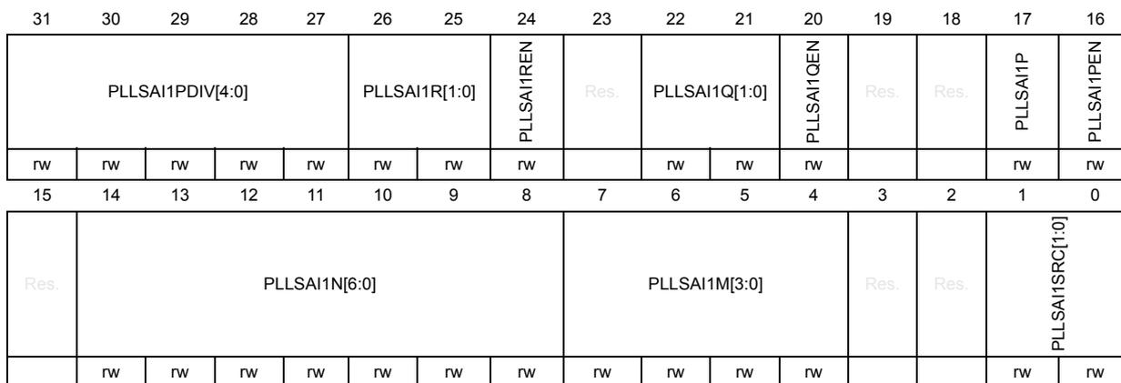
9.8.5 RCC PLLSA1 configuration register (RCC_PLLSA1CFGR)
Address offset: 0x010
Reset value: 0x0000 1000
Access: no wait state, word, half-word and byte access
This register is used to configure the PLLSA1 clock outputs according to the formulas:
- • \( f(\text{VCOSAI1 clock}) = f(\text{PLL clock input}) * (\text{PLLSAI1N} / \text{PLLM}) \)
- • \( f(\text{PLLSAI1\_P}) = f(\text{VCOSAI1 clock}) / \text{PLLSAI1PDIV} \)
- • \( f(\text{PLLSAI1\_Q}) = f(\text{VCOSAI1 clock}) / \text{PLLSAI1Q} \)
- • \( f(\text{PLLSAI1\_R}) = f(\text{VCOSAI1 clock}) / \text{PLLSAI1R} \)
| 31 | 30 | 29 | 28 | 27 | 26 | 25 | 24 | 23 | 22 | 21 | 20 | 19 | 18 | 17 | 16 |
| PLLSAI1PDIV[4:0] | PLLSAI1R[1:0] | PLLSAI1REN | Res. | PLLSAI1Q[1:0] | PLLSAI1QEN | Res. | Res. | PLLSAI1P | PLLSAI1PEN | ||||||
| rw | rw | rw | rw | rw | rw | rw | rw | rw | rw | rw | rw | rw | |||
| 15 | 14 | 13 | 12 | 11 | 10 | 9 | 8 | 7 | 6 | 5 | 4 | 3 | 2 | 1 | 0 |
| Res. | PLLSAI1N[6:0] | PLLSAI1M[3:0] | Res. | Res. | PLLSAI1SRC[1:0] | ||||||||||
| rw | rw | rw | rw | rw | rw | rw | rw | rw | rw | rw | rw | rw | |||
Bits 31:27 PLLSAI1PDIV[4:0] : PLLSA1 division factor for PLLSA1CLK
Set and cleared by software to control the SAI1 or SAI2 clock frequency.
PLLSAI1CLK output clock frequency = VCOSAI1 frequency / PLLSA1PDIV.
00000: PLLSA1CLK controlled by PLLSA1P bit
00001: reserved
00010: PLLSA1CLK = VCOSAI1 / 2
....
11111: PLLSA1CLK = VCOSAI1 / 31
Note: This bit can be written only when the PLLSA1 is disabled.
Bits 26:25 PLLSAI1R[1:0] : PLLSA1 division factor for PLLADC1CLK (ADC clock)
Set and cleared by software to control the frequency of the PLLSA1 output clock
PLLADC1CLK. This output can be selected as ADC clock.
These bits can be written only if PLLSA1 is disabled.
PLLADC1CLK output clock frequency = VCOSAI1 frequency / PLLSA1R, with
PLLSAI1R = 2, 4, 6, or 8.
00: PLLSA1R = 2
01: PLLSA1R = 4
10: PLLSA1R = 6
11: PLLSA1R = 8
Bit 24 PLL1SAI1REN : PLL1SAI1 PLLADC1CLK output enable
Set and reset by software to enable the PLLADC1CLK output of the PLL1SAI1 (used as clock for ADC).
In order to save power, when the PLLADC1CLK output of the PLL1SAI1 is not used, the value of PLL1SAI1REN must be 0.
0: PLLADC1CLK output disabled
1: PLLADC1CLK output enabled
Bit 23 Reserved, must be kept at reset value.
Bits 22:21 PLL1SAI1Q[1:0] : PLL1SAI1 division factor for PLL48M2CLK (48 MHz clock)
Set and cleared by software to control the frequency of the PLL1SAI1 output clock
PLL48M2CLK. This output can be selected for USB, RNG, SDMMC (48 MHz clock). These bits can be written only if PLL1SAI1 is disabled.
PLL48M2CLK output clock frequency = VCOSAI1 frequency / PLL1SAI1Q with
PLL1SAI1Q = 2, 4, 6, or 8
00: PLL1SAI1Q = 2
01: PLL1SAI1Q = 4
10: PLL1SAI1Q = 6
11: PLL1SAI1Q = 8
Caution: The software must set these bits correctly not to exceed 110 MHz on this domain.
Bit 20 PLL1SAI1QEN : PLL1SAI1 PLL48M2CLK output enable
Set and reset by software to enable the PLL48M2CLK output of the PLL1SAI1.
In order to save power, when the PLL48M2CLK output of the PLL1SAI1 is not used, the value of PLL1SAI1QEN must be 0.
0: PLL48M2CLK output disabled
1: PLL48M2CLK output enabled
Bits 19:18 Reserved, must be kept at reset value.
Bit 17 PLL1SAI1P : PLL1SAI1 division factor for PLL1SAI1CLK (SAI1 or SAI2 clock).
Set and cleared by software to control the frequency of the PLL1SAI1 output clock
PLL1SAI1CLK. This output can be selected for SAI1 or SAI2. These bits can be written only if PLL1SAI1 is disabled.
When the PLL1SAI1PDIV[4:0] is set to 0x0, PLL1SAI1CLK output clock frequency = VCOSAI1 frequency / PLL1SAI1P with PLL1SAI1P = 7, or 17
0: PLL1SAI1P = 7
1: PLL1SAI1P = 17
Bit 16 PLL1SAI1PEN : PLL1SAI1 PLL1SAI1CLK output enable
Set and reset by software to enable the PLL1SAI1CLK output of the PLL1SAI1.
In order to save power, when the PLL1SAI1CLK output of the PLL1SAI1 is not used, the value of PLL1SAI1PEN must be 0.
0: PLL1SAI1CLK output disabled
1: PLL1SAI1CLK output enabled
Bit 15 Reserved, must be kept at reset value.
Bits 14:8 PLLSAI1N[6:0] : PLLSAI1 multiplication factor for VCO
Set and cleared by software to control the multiplication factor of the VCO.
These bits can be written only when the PLLSAI1 is disabled.
VCOSAI1 output frequency = VCOSAI1 input frequency x PLLSAI1N, with \( 8 \leq \text{PLLSAI1N} \leq 86 \) .
0000000: PLLSAI1N = 0 wrong configuration
0000001: PLLSAI1N = 1 wrong configuration
...
0000111: PLLSAI1N = 7 wrong configuration
0001000: PLLSAI1N = 8
0001001: PLLSAI1N = 9
...
1111111: PLLSAI1N = 127
Caution: The software must set correctly these bits to ensure that the VCO output frequency is between 64 and 344 MHz.
Bits 7:4 PLLSAI1M[3:0] : Division factor for PLLSAI1 input clock
Set and reset by software to divide the PLLSAI1 input clock before the VCO.
These bits can be written only when PLLSAI1 is disabled.
VCO input frequency = PLLSAI1 input clock frequency / PLLSAI1M with \( 1 \leq \text{PLLSAI1M} \leq 16 \) .
0000: PLLSAI1M = 1
0001: PLLSAI1M = 2
0010: PLLSAI1M = 3
0011: PLLSAI1M = 4
0100: PLLSAI1M = 5
0101: PLLSAI1M = 6
0110: PLLSAI1M = 7
0111: PLLSAI1M = 8
1000: PLLSAI1M = 9
...
1111: PLLSAI1M = 16
Caution: The software must set these bits correctly to ensure that the VCO input frequency ranges from 2.66 to 8 MHz.
Bits 3:2 Reserved, must be kept at reset value.
Bits 1:0 PLLSAI1SRC[1:0] : Main PLLSAI1 entry clock source
Set and cleared by software to select PLLSAI1 clock source.
These bits can be written only when PLLSAI1 is disabled.
In order to save power, when PLLSAI1 is not used, the value of PLLSAI1 must be 00.
00: No clock sent to PLLSAI1
01: MSI clock selected as PLLSAI1 clock entry
10: HSI16 clock selected as PLLSAI1 clock entry
11: HSE clock selected as PLLSAI1 clock entry
9.8.6 RCC PLLSAI2 configuration register (RCC_PLLSAI2CFGR)
Address offset: 0x014
Reset value: 0x0000 1000
Access: no wait state, word, half-word and byte access
This register is used to configure the PLLSAI2 clock outputs according to the formulas:
- • \( f(\text{VCOSAI2 clock}) = f(\text{PLL clock input}) \times (\text{PLLSAI2N} / \text{PLLM}) \)
- • \( f(\text{PLLSAI2\_P}) = f(\text{VCOSAI2 clock}) / \text{PLLSAI2P} \)
- • \( f(\text{PLLSAI2\_R}) = f(\text{VCOSAI2 clock}) / \text{PLLSAI2R} \)
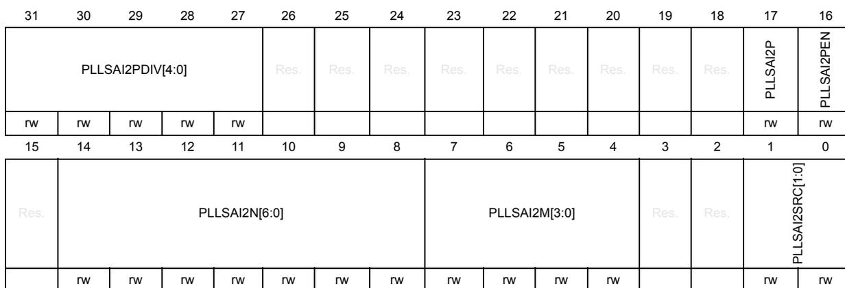
| 31 | 30 | 29 | 28 | 27 | 26 | 25 | 24 | 23 | 22 | 21 | 20 | 19 | 18 | 17 | 16 |
| PLLSAI2PDIV[4:0] | Res. | Res. | Res. | Res. | Res. | Res. | Res. | Res. | Res. | PLLSAI2P | PLLSAI2PEN | ||||
| rw | rw | rw | rw | rw | rw | rw | |||||||||
| 15 | 14 | 13 | 12 | 11 | 10 | 9 | 8 | 7 | 6 | 5 | 4 | 3 | 2 | 1 | 0 |
| Res. | PLLSAI2N[6:0] | PLLSAI2M[3:0] | Res. | Res. | PLLSAI2SRC[1:0] | ||||||||||
| rw | rw | rw | rw | rw | rw | rw | rw | rw | rw | rw | rw | rw | |||
Bits 31:27 PLLSAI2PDIV[4:0] : PLLSAI2 division factor for PLLSAI2CLK
Set and cleared by software to control the SAI1 or SAI2 clock frequency.
\( \text{PLLSAI2CLK output clock frequency} = \text{VCOSAI2 frequency} / \text{PLLSAI2PDIV} \) .
00000: PLLSAI2CLK controlled by the bit PLLSAI2P
00001: reserved
00010: PLLSAI2CLK = VCOSAI2 / 2
....
11111: PLLSAI2CLK = VCOSAI2 / 31
Bits 26:18 Reserved, must be kept at reset value.
Bit 17 PLLSAI2P : PLLSAI2 division factor for PLLSAI2CLK (SAI1 or SAI2 clock).
Set and cleared by software to control the frequency of the PLLSAI2 output clock PLLSAI2CLK. This output can be selected for SAI1 or SAI2.
These bits can be written only if PLLSAI2 is disabled.
When the PLLSAI2PDIV[4:0] is set to 0x0, PLLSAI2CLK output clock frequency = VCOSAI2 frequency / PLLSAI2P with PLLSAI2P = 7 or 17.
0: PLLSAI2P = 7
1: PLLSAI2P = 17
Bit 16 PLLSAI2PEN : PLLSAI2 PLLSAI2CLK output enable
Set and reset by software to enable the PLLSAI2CLK output of the PLLSAI2.
In order to save power, when the PLLSAI2CLK output of the PLLSAI2 is not used, the value of PLLSAI2PEN must be 0.
0: PLLSAI2CLK output disabled
1: PLLSAI2CLK output enabled
Bit 15 Reserved, must be kept at reset value.
Bits 14:8 PLLSAI2N[6:0] : PLLSAI2 multiplication factor for VCO
Set and cleared by software to control the multiplication factor of the VCO.
These bits can be written only when the PLLSAI2 is disabled.
VCOSAI2 output frequency = VCOSAI2 input frequency x PLLSAI2N, with
\( 8 \leq \text{PLLSAI2N} \leq 86 \)
0000000: PLLSAI2N = 0 wrong configuration
0000001: PLLSAI2N = 1 wrong configuration
...
0000111: PLLSAI2N = 7 wrong configuration
0001000: PLLSAI2N = 8
0001001: PLLSAI2N = 9
...
1111111: PLLSAI2N = 127 wrong configuration
Caution: The software must set correctly these bits to ensure that the VCO output frequency is between 64 and 344 MHz.
Bits 7:4 PLLSAI2M[3:0] : Division factor for PLLSAI2 input clock
Set and reset by software to divide the PLLSAI2 input clock before the VCO.
These bits can be written only when PLLSAI2 is disabled.
VCO input frequency = PLLSAI2 input clock frequency / PLLM with \( 1 \leq \text{PLLSAI2N} \leq 16 \)
0000: PLLSAI2M = 1
0001: PLLSAI2M = 2
0010: PLLSAI2M = 3
0011: PLLSAI1M = 4
0100: PLLSAI2M = 5
0101: PLLSAI2M = 6
0110: PLLSAI2M = 7
0111: PLLSAI2M = 8
1000: PLLSAI2M = 9
...
1111: PLLSAI2M = 16
Caution: The software must set these bits correctly to ensure that the VCO input frequency is between 2.66 to 8 MHz.
Bits 3:2 Reserved, must be kept at reset value.
Bits 1:0 PLLSAI2SRC[1:0] : Main PLLSAI2 entry clock source
Set and cleared by software to select PLLSAI2 clock source.
These bits can be written only when PLLSAI2 is disabled.
In order to save power, when PLLSAI2 is not used, the value of PLLSAI2 must be 00.
00: No clock sent to PLLSAI2
01: MSI clock selected as PLLSAI2 clock entry
10: HSI16 clock selected as PLLSAI2 clock entry
11: HSE clock selected as PLLSAI2 clock entry
9.8.7 RCC clock interrupt enable register (RCC_CIER)
Address offset: 0x018
Reset value: 0x0000 0000
Access: no wait state, word, half-word and byte access
| 31 | 30 | 29 | 28 | 27 | 26 | 25 | 24 | 23 | 22 | 21 | 20 | 19 | 18 | 17 | 16 |
|---|---|---|---|---|---|---|---|---|---|---|---|---|---|---|---|
| Res. | Res. | Res. | Res. | Res. | Res. | Res. | Res. | Res. | Res. | Res. | Res. | Res. | Res. | Res. | Res. |
| 15 | 14 | 13 | 12 | 11 | 10 | 9 | 8 | 7 | 6 | 5 | 4 | 3 | 2 | 1 | 0 |
| Res. | Res. | Res. | Res. | Res. | HSI48RDYIE | Res. | Res. | PLL2SAI2RDYIE | PLL1SAI1RDYIE | PLL1RDYIE | HSERDYIE | HSIRDYIE | MSIRDYIE | LSERDYIE | LSIRDYIE |
| r/w | r/w | r/w | r/w | r/w | r/w | r/w | r/w | r/w |
Bits 31:11 Reserved, must be kept at reset value.
Bit 10 HSI48RDYIE : HSI48 ready interrupt enable
Set and cleared by software to enable/disable interrupt caused by the internal HSI48 oscillator.
0: HSI48 ready interrupt disabled
1: HSI48 ready interrupt enabled
Bit 9 Reserved, must be kept at reset value.
Bit 8 Reserved, must be kept at reset value.
Bit 7 PLL2SAI2RDYIE : PLL2SAI2 ready interrupt enable
Set and cleared by software to enable/disable interrupt caused by PLL2SAI2 lock.
0: PLL2SAI2 lock interrupt disabled
1: PLL2SAI2 lock interrupt enabled
Bit 6 PLL1SAI1RDYIE : PLL1SAI1 ready interrupt enable
Set and cleared by software to enable/disable interrupt caused by PLL1SAI1L lock.
0: PLL1SAI1 lock interrupt disabled
1: PLL1SAI1 lock interrupt enabled
Bit 5 PLL1RDYIE : PLL ready interrupt enable
Set and cleared by software to enable/disable interrupt caused by PLL lock.
0: PLL lock interrupt disabled
1: PLL lock interrupt enabled
Bit 4 HSERDYIE : HSE ready interrupt enable
Set and cleared by software to enable/disable interrupt caused by the HSE oscillator stabilization.
0: HSE ready interrupt disabled
1: HSE ready interrupt enabled
Bit 3 HSIRDYIE : HSI16 ready interrupt enable
Set and cleared by software to enable/disable interrupt caused by the HSI16 oscillator stabilization.
0: HSI16 ready interrupt disabled
1: HSI16 ready interrupt enabled
Bit 2 MSIRDYIE : MSI ready interrupt enable
Set and cleared by software to enable/disable interrupt caused by the MSI oscillator stabilization.
0: MSI ready interrupt disabled
1: MSI ready interrupt enabled
Bit 1 LSERDYIE : LSE ready interrupt enable
Set and cleared by software to enable/disable interrupt caused by the LSE oscillator stabilization.
0: LSE ready interrupt disabled
1: LSE ready interrupt enabled
Bit 0 LSIRDYIE : LSI ready interrupt enable
Set and cleared by software to enable/disable interrupt caused by the LSI oscillator stabilization.
0: LSI ready interrupt disabled
1: LSI ready interrupt enabled
9.8.8 RCC clock interrupt flag register (RCC_CIFR)
Address offset: 0x01C
Reset value: 0x0000 0000
Access: no wait state, word, half-word and byte access
| 31 | 30 | 29 | 28 | 27 | 26 | 25 | 24 | 23 | 22 | 21 | 20 | 19 | 18 | 17 | 16 |
|---|---|---|---|---|---|---|---|---|---|---|---|---|---|---|---|
| Res. | Res. | Res. | Res. | Res. | Res. | Res. | Res. | Res. | Res. | Res. | Res. | Res. | Res. | Res. | Res. |
| 15 | 14 | 13 | 12 | 11 | 10 | 9 | 8 | 7 | 6 | 5 | 4 | 3 | 2 | 1 | 0 |
| Res. | Res. | Res. | Res. | Res. | HSI48RDYF | Res. | CSSF | PLLISA2RDYF | PLLISA1RDYF | PLLRDYF | HSERDYF | HSIRDYF | MSIRDYF | LSERDYF | LSIRDYF |
| r | r | r | r | r | r | r | r | r | r |
Bits 31:11 Reserved, must be kept at reset value.
Bit 10 HSI48RDYF : HSI48 ready interrupt flag
Set by hardware when the HSI48 clock becomes stable and HSI48RDYIE is set in a response to setting the HSI48ON (refer to RCC clock recovery RC register (RCC_CRRCR) ).
Cleared by software setting the HSI48RDYC bit.
0: No clock ready interrupt caused by the HSI48 oscillator
1: Clock ready interrupt caused by the HSI48 oscillator
Bit 9 Reserved, must be kept at reset value.
Bit 8 CSSF : Clock security system interrupt flag
Set by hardware when a failure is detected in the HSE oscillator.
Cleared by software setting the CSSC bit.
0: No clock security interrupt caused by HSE clock failure
1: Clock security interrupt caused by HSE clock failure
Bit 7 PLLSAI2RDYF: PLLSAI2 ready interrupt flagSet by hardware when the PLLSAI2 locks and PLLSAI2RDYE is set.
Cleared by software setting the PLLSAI2RDYC bit.
0: No clock ready interrupt caused by PLLSAI2 lock
1: Clock ready interrupt caused by PLLSAI2 lock
Bit 6 PLLSAI1RDYF: PLLSAI1 ready interrupt flagSet by hardware when the PLLSAI1 locks and PLLSAI1RDYE is set.
Cleared by software setting the PLLSAI1RDYC bit.
0: No clock ready interrupt caused by PLLSAI1 lock
1: Clock ready interrupt caused by PLLSAI1 lock
Bit 5 PLLRDYF: PLL ready interrupt flagSet by hardware when the PLL locks and PLLRDYE is set.
Cleared by software setting the PLLRDYC bit.
0: No clock ready interrupt caused by PLL lock
1: Clock ready interrupt caused by PLL lock
Bit 4 HSERDYF: HSE ready interrupt flagSet by hardware when the HSE clock becomes stable and HSERDYE is set.
Cleared by software setting the HSERDYC bit.
0: No clock ready interrupt caused by the HSE oscillator
1: Clock ready interrupt caused by the HSE oscillator
Bit 3 HSIRDYF: HSI16 ready interrupt flagSet by hardware when the HSI16 clock becomes stable and HSIRDYE is set in a response to setting the HSION (refer to RCC clock control register (RCC_CR) ). When HSION is not set but the HSI16 oscillator is enabled by the peripheral through a clock request, this bit is not set and no interrupt is generated.
Cleared by software setting the HSIRDYC bit.
0: No clock ready interrupt caused by the HSI16 oscillator
1: Clock ready interrupt caused by the HSI16 oscillator
Bit 2 MSIRDYF: MSI ready interrupt flagSet by hardware when the MSI clock becomes stable and MSIRDYE is set.
Cleared by software setting the MSIRDYC bit.
0: No clock ready interrupt caused by the MSI oscillator
1: Clock ready interrupt caused by the MSI oscillator
Bit 1 LSERDYF: LSE ready interrupt flagSet by hardware when the LSE clock becomes stable and LSERDYE is set.
Cleared by software setting the LSERDYC bit.
0: No clock ready interrupt caused by the LSE oscillator
1: Clock ready interrupt caused by the LSE oscillator
Bit 0 LSIRDYF: LSI ready interrupt flagSet by hardware when the LSI clock becomes stable and LSIRDYE is set.
Cleared by software setting the LSIRDYC bit.
0: No clock ready interrupt caused by the LSI oscillator
1: Clock ready interrupt caused by the LSI oscillator
9.8.9 RCC clock interrupt clear register (RCC_CICR)
Address offset: 0x020
Reset value: 0x0000 0000
Access: no wait state, word, half-word and byte access
| 31 | 30 | 29 | 28 | 27 | 26 | 25 | 24 | 23 | 22 | 21 | 20 | 19 | 18 | 17 | 16 |
|---|---|---|---|---|---|---|---|---|---|---|---|---|---|---|---|
| Res. | Res. | Res. | Res. | Res. | Res. | Res. | Res. | Res. | Res. | Res. | Res. | Res. | Res. | Res. | Res. |
| 15 | 14 | 13 | 12 | 11 | 10 | 9 | 8 | 7 | 6 | 5 | 4 | 3 | 2 | 1 | 0 |
| Res. | Res. | Res. | Res. | Res. | HSI48RDYC | Res. | CSSC | PLL2SAI2RDYC | PLL1SAI1RDYC | PLL1RDYC | HSERDYC | HSIRDYC | MSIRDYC | LSERDYC | LSIRDYC |
| w | w | w | w | w | w | w | w | w | w |
Bits 31:11 Reserved, must be kept at reset value.
Bit 10 HSI48RDYC : HSI48 oscillator ready interrupt clear
This bit is set by software to clear the HSI48RDYF flag.
0: No effect
1: Clear the HSI48RDYC flag
Bit 9 Reserved, must be kept at reset value.
Bit 8 CSSC : Clock security system interrupt clear
This bit is set by software to clear the CSSF flag.
0: No effect
1: Clear CSSF flag
Bit 7 PLL2SAI2RDYC : PLL2SAI2 ready interrupt clear
This bit is set by software to clear the PLL2SAI2RDYF flag.
0: No effect
1: Clear PLL2SAI2RDYF flag
Bit 6 PLL1SAI1RDYC : PLL1SAI1 ready interrupt clear
This bit is set by software to clear the PLL1SAI1RDYF flag.
0: No effect
1: Clear PLL1SAI1RDYF flag
Bit 5 PLL1RDYC : PLL ready interrupt clear
This bit is set by software to clear the PLLRDYF flag.
0: No effect
1: Clear PLLRDYF flag
Bit 4 HSERDYC : HSE ready interrupt clear
This bit is set by software to clear the HSERDYF flag.
0: No effect
1: Clear HSERDYF flag
Bit 3 HSIRDYC : HSI16 ready interrupt clear
This bit is set software to clear the HSIRDYF flag.
0: No effect
1: Clear HSIRDYF flag
- Bit 2
MSIRDYC
: MSI ready interrupt clear
This bit is set by software to clear the MSIRDYF flag.
0: No effect
1: MSIRDYF cleared - Bit 1
LSERDYC
: LSE ready interrupt clear
This bit is set by software to clear the LSERDYF flag.
0: No effect
1: LSERDYF cleared - Bit 0
LSIRDYC
: LSI ready interrupt clear
This bit is set by software to clear the LSIRDYF flag.
0: No effect
1: LSIRDYF cleared
9.8.10 RCC AHB1 peripheral reset register (RCC_AHB1RSTR)
Address offset: 0x028
Reset value: 0x0000 0000
Access: no wait state, word, half-word and byte access
| 31 | 30 | 29 | 28 | 27 | 26 | 25 | 24 | 23 | 22 | 21 | 20 | 19 | 18 | 17 | 16 |
|---|---|---|---|---|---|---|---|---|---|---|---|---|---|---|---|
| Res. | Res. | Res. | Res. | Res. | Res. | Res. | Res. | Res. | Res. | Res. | Res. | Res. | Res. | Res. | TSCRST |
| w | |||||||||||||||
| 15 | 14 | 13 | 12 | 11 | 10 | 9 | 8 | 7 | 6 | 5 | 4 | 3 | 2 | 1 | 0 |
| Res. | Res. | Res. | CRCCRST | Res. | Res. | Res. | FLASHRST | Res. | Res. | Res. | Res. | Res. | DMAMUX1RST | DMA2RST | DMA1RST |
| rw | rw | rw | rw | rw |
Bits 31:17 Reserved, must be kept at reset value.
- Bit 16
TSCRST
: Touch sensing controller reset
Set and cleared by software.
0: No effect
1: Reset TSC
Bits 15:13 Reserved, must be kept at reset value.
- Bit 12
CRCCRST
: CRC reset
Set and cleared by software.
0: No effect
1: Reset CRC
Bits 11:9 Reserved, must be kept at reset value.
- Bit 8
FLASHRST
: Flash memory interface reset
Set and cleared by software. This bit can be activated only when the flash memory is in power down mode.
0: No effect
1: Reset flash memory interface
Bits 7:3 Reserved, must be kept at reset value.
Bit 2 DMAMUX1RST : DMAMUX1 reset
Set and cleared by software.
0: No effect
1: Reset DMAMUX1
Bit 1 DMA2RST : DMA2 reset
Set and cleared by software.
0: No effect
1: Reset DMA2
Bit 0 DMA1RST : DMA1 reset
Set and cleared by software.
0: No effect
1: Reset DMA1
9.8.11 RCC AHB2 peripheral reset register (RCC_AHB2RSTR)
Address offset: 0x02C
Reset value: 0x0000 0000
Access: no wait state, word, half-word and byte access
| 31 | 30 | 29 | 28 | 27 | 26 | 25 | 24 | 23 | 22 | 21 | 20 | 19 | 18 | 17 | 16 |
|---|---|---|---|---|---|---|---|---|---|---|---|---|---|---|---|
| Res. | Res. | Res. | Res. | Res. | Res. | Res. | Res. | Res. | SDMMC1RST | OTFDEC1RST | Res. | PKARST | RNGRST | HASHRST | AESRST |
| rw | rw | rw | rw | rw | rw | ||||||||||
| 15 | 14 | 13 | 12 | 11 | 10 | 9 | 8 | 7 | 6 | 5 | 4 | 3 | 2 | 1 | 0 |
| Res. | Res. | ADCRST | Res. | Res. | Res. | Res. | Res. | GPIOHRST | GPIOGRST | GPIOFRST | GPIOERST | GPIODRST | GPIOCRST | GPIOBRST | GPIOARST |
| rw | rw | rw | rw | rw | rw | rw | rw | rw |
Bits 31:23 Reserved, must be kept at reset value.
Bit 22 SDMMC1RST : SDMMC1 reset
Set and cleared by software.
0: No effect
1: Reset SDMMC1
Bit 21 OTFDEC1RST : OTFDEC reset
Set and cleared by software.
0: No effect
1: Reset OTFDEC
Bit 20 Reserved, must be kept at reset value.
Bit 19 PKARST : PKA reset
Set and cleared by software.
0: No effect
1: Reset PKA
Bit 18 RNGRST : Random number generator reset
Set and cleared by software.
0: No effect
1: Reset RNG
Bit 17 HASHRST : Hash reset
Set and cleared by software.
0: No effect
1: Reset HASH
Bit 16 AESRST : AES hardware accelerator reset
Set and cleared by software.
0: No effect
1: Reset AES
Bits 15:14 Reserved, must be kept at reset value.
Bit 13 ADCRST : ADC reset
Set and cleared by software.
0: No effect
1: Reset ADC interface
Bits 12:8 Reserved, must be kept at reset value.
Bit 7 GPIOHRST : IO port H reset
Set and cleared by software.
0: No effect
1: Reset IO port H
Bit 6 GPIOGRST : IO port G reset
Set and cleared by software.
0: No effect
1: Reset IO port G
Bit 5 GPIOFRST : IO port F reset
Set and cleared by software.
0: No effect
1: Reset IO port F
Bit 4 GPIOERST : IO port E reset
Set and cleared by software.
0: No effect
1: Reset IO port E
Bit 3 GPIODRST : IO port D reset
Set and cleared by software.
0: No effect
1: Reset IO port D
- Bit 2
GPIOCRST
: IO port C reset
Set and cleared by software.
0: No effect
1: Reset IO port C - Bit 1
GPIObRST
: IO port B reset
Set and cleared by software.
0: No effect
1: Reset IO port B - Bit 0
GPIoARST
: IO port A reset
Set and cleared by software.
0: No effect
1: Reset IO port A
9.8.12 RCC AHB3 peripheral reset register (RCC_AHB3RSTR)
Address offset: 0x030
Reset value: 0x0000 0000
Access: no wait state, word, half-word and byte access
| 31 | 30 | 29 | 28 | 27 | 26 | 25 | 24 | 23 | 22 | 21 | 20 | 19 | 18 | 17 | 16 |
|---|---|---|---|---|---|---|---|---|---|---|---|---|---|---|---|
| Res. | Res. | Res. | Res. | Res. | Res. | Res. | Res. | Res. | Res. | Res. | Res. | Res. | Res. | Res. | Res. |
| 15 | 14 | 13 | 12 | 11 | 10 | 9 | 8 | 7 | 6 | 5 | 4 | 3 | 2 | 1 | 0 |
| Res. | Res. | Res. | Res. | Res. | Res. | Res. | OSPI1RST | Res. | Res. | Res. | Res. | Res. | Res. | Res. | FMCRST |
| rw | rw |
Bits 31:9 Reserved, must be kept at reset value.
- Bit 8
OSPI1RST
: OCTOSPI1 memory interface reset
Set and cleared by software.
0: No effect
1: Reset OCTOSPI1
Bits 7:1 Reserved, must be kept at reset value.
- Bit 0
FMCRST
: Flexible memory controller reset
Set and cleared by software.
0: No effect
1: Reset FMC
9.8.13 RCC APB1 peripheral reset register 1 (RCC_APB1RSTR1)
Address offset: 0x038
Reset value: 0x0000 0000
Access: no wait state, word, half-word and byte access
| 31 | 30 | 29 | 28 | 27 | 26 | 25 | 24 | 23 | 22 | 21 | 20 | 19 | 18 | 17 | 16 |
|---|---|---|---|---|---|---|---|---|---|---|---|---|---|---|---|
| LPTIM1RST | OPAMP_RST | DAC1RST | PWRRST | Res. | Res. | Res. | CRSRST | I2C3RST | I2C2RST | I2C1RST | UART5RST | UART4RST | USART3RST | USART2RST | Res. |
| rw | rw | rw | rw | rw | rw | rw | rw | rw | rw | rw | rw |
| 15 | 14 | 13 | 12 | 11 | 10 | 9 | 8 | 7 | 6 | 5 | 4 | 3 | 2 | 1 | 0 |
|---|---|---|---|---|---|---|---|---|---|---|---|---|---|---|---|
| SPI3RST | SPI2RST | Res. | Res. | Res. | Res. | Res. | Res. | Res. | Res. | TIM7RST | TIM6RST | TIM5RST | TIM4RST | TIM3RST | TIM2RST |
| rw | rw | rw | rw | rw | rw | rw | rw |
Bit 31 LPTIM1RST : Low-power timer 1 reset
Set and cleared by software.
0: No effect
1: Reset LPTIM1
Bit 30 OPAMP_RST : OPAMP interface reset
Set and cleared by software.
0: No effect
1: Reset OPAMP interface
Bit 29 DAC1RST : DAC1 interface reset
Set and cleared by software.
0: No effect
1: Reset DAC1 interface
Bit 28 PWRRST : Power interface reset
Set and cleared by software.
0: No effect
1: Reset PWR
Bits 27:25 Reserved, must be kept at reset value.
Bit 24 CRSRST : CRS reset
Set and cleared by software.
0: No effect
1: Reset the CRS
Bit 23 I2C3RST : I2C3 reset
Set and reset by software.
0: No effect
1: Reset I2C3
Bit 22 I2C2RST : I2C2 reset
Set and cleared by software.
0: No effect
1: Reset I2C2
- Bit 21
I2C1RST
: I2C1 reset
Set and cleared by software.
0: No effect
1: Reset I2C1 - Bit 20
UART5RST
: UART5 reset
Set and cleared by software.
0: No effect
1: Reset UART5 - Bit 19
UART4RST
: UART4 reset
Set and cleared by software.
0: No effect
1: Reset UART4 - Bit 18
USART3RST
: USART3 reset
Set and cleared by software.
0: No effect
1: Reset USART3 - Bit 17
USART2RST
: USART2 reset
Set and cleared by software.
0: No effect
1: Reset USART2 - Bit 16 Reserved, must be kept at reset value.
- Bit 15
SPI3RST
: SPI3 reset
Set and cleared by software.
0: No effect
1: Reset SPI3 - Bit 14
SPI2RST
: SPI2 reset
Set and cleared by software.
0: No effect
1: Reset SPI2 - Bits 13:6 Reserved, must be kept at reset value.
- Bit 5
TIM7RST
: TIM7 timer reset
Set and cleared by software.
0: No effect
1: Reset TIM7 - Bit 4
TIM6RST
: TIM6 timer reset
Set and cleared by software.
0: No effect
1: Reset TIM6 - Bit 3
TIM5RST
: TIM5 timer reset
Set and cleared by software.
0: No effect
1: Reset TIM5
- Bit 2
TIM4RST
: TIM3 timer reset
Set and cleared by software.
0: No effect
1: Reset TIM3 - Bit 1
TIM3RST
: TIM3 timer reset
Set and cleared by software.
0: No effect
1: Reset TIM3 - Bit 0
TIM2RST
: TIM2 timer reset
Set and cleared by software.
0: No effect
1: Reset TIM2
9.8.14 RCC APB1 peripheral reset register 2 (RCC_APB1RSTR2)
Address offset: 0x03C
Reset value: 0x0000 0000
Access: no wait state, word, half-word and byte access
| 31 | 30 | 29 | 28 | 27 | 26 | 25 | 24 | 23 | 22 | 21 | 20 | 19 | 18 | 17 | 16 |
|---|---|---|---|---|---|---|---|---|---|---|---|---|---|---|---|
| Res. | Res. | Res. | Res. | Res. | Res. | Res. | Res. | UCPD1RST | Res. | USBFSRST | Res. | Res. | Res. | Res. | Res. |
| 15 | 14 | 13 | 12 | 11 | 10 | 9 | 8 | 7 | 6 | 5 | 4 | 3 | 2 | 1 | 0 |
| Res. | Res. | Res. | Res. | Res. | Res. | FDCAN1RST | Res. | Res. | LPTIM3RST | LPTIM2RST | Res. | Res. | Res. | I2C4RST | LPUART1RST |
| rw | rw | rw | rw | rw |
Bits 31:24 Reserved, must be kept at reset value.
- Bit 23
UCPD1RST
: UCPD1 reset
Set and cleared by software.
0: No effect
1: Reset UCPD1
Bit 22 Reserved, must be kept at reset value.
- Bit 21
USBFSRST
: USB FS reset
Set and cleared by software.
0: No effect
1: Reset USB FS
Bits 20:10 Reserved, must be kept at reset value.
- Bit 9
FDCAN1RST
: FDCAN1 reset
Set and cleared by software.
0: No effect
1: Reset FDCAN1
Bits 8:7 Reserved, must be kept at reset value.
Bit 6 LPTIM3RST : LPTIM3 reset
Set and cleared by software.
0: No effect
1: Reset LPTIM3
Bit 5 LPTIM2RST : LPTIM2 reset
Set and cleared by software.
0: No effect
1: Reset LPTIM2
Bits 4:2 Reserved, must be kept at reset value.
Bit 1 I2C4RST : I2C4 reset
Set and cleared by software
0: No effect
1: Reset I2C4
Bit 0 LPUART1RST : Low-power UART 1 reset
Set and cleared by software.
0: No effect
1: Reset LPUART1
9.8.15 RCC APB2 peripheral reset register (RCC_APB2RSTR)
Address offset: 0x040
Reset value: 0x0000 0000
Access: no wait state, word, half-word and byte access
| 31 | 30 | 29 | 28 | 27 | 26 | 25 | 24 | 23 | 22 | 21 | 20 | 19 | 18 | 17 | 16 |
|---|---|---|---|---|---|---|---|---|---|---|---|---|---|---|---|
| Res. | Res. | Res. | Res. | Res. | Res. | Res. | DFSDM1RST | Res. | SAI2RST | SAI1RST | Res. | Res. | TIM17RST | TIM16RST | TIM15RST |
| rw | rw | rw | rw | rw | rw | ||||||||||
| 15 | 14 | 13 | 12 | 11 | 10 | 9 | 8 | 7 | 6 | 5 | 4 | 3 | 2 | 1 | 0 |
| Res. | USART1RST | TIM8RST | SPI1RST | TIM1RST | Res. | Res. | Res. | Res. | Res. | Res. | Res. | Res. | Res. | Res. | SYSCFGGRST |
| rw | rw | rw | rw | rw |
Bits 31:25 Reserved, must be kept at reset value.
Bit 24 DFSDM1RST : Digital filters for sigma-delta modulators (DFSDM1) reset
Set and cleared by software.
0: No effect
1: Reset DFSDM1
Bit 23 Reserved, must be kept at reset value.
Bit 22 SAI2RST : Serial audio interface 2 (SAI2) reset
Set and cleared by software.
0: No effect
1: Reset SAI2
Bit 21 SAI1RST : Serial audio interface 1 (SAI1) reset
Set and cleared by software.
0: No effect
1: Reset SAI1
Bits 20:19 Reserved, must be kept at reset value.
Bit 18 TIM17RST : TIM17 timer reset
Set and cleared by software.
0: No effect
1: Reset TIM17
Bit 17 TIM16RST : TIM16 timer reset
Set and cleared by software.
0: No effect
1: Reset TIM16
Bit 16 TIM15RST : TIM15 timer reset
Set and cleared by software.
0: No effect
1: Reset TIM15
Bit 15 Reserved, must be kept at reset value.
Bit 14 USART1RST : USART1 reset
Set and cleared by software.
0: No effect
1: Reset USART1
Bit 13 TIM8RST : TIM8 timer reset
Set and cleared by software.
0: No effect
1: Reset TIM8
Bit 12 SPI1RST : SPI1 reset
Set and cleared by software.
0: No effect
1: Reset SPI1
Bit 11 TIM1RST : TIM1 timer reset
Set and cleared by software.
0: No effect
1: Reset TIM1
Bits 10:1 Reserved, must be kept at reset value.
Bit 0 SYSCFGRST : SYSCFG + COMP + VREFBUF reset
0: No effect
1: Reset SYSCFG + COMP + VREFBUF
9.8.16 RCC AHB1 peripheral clock enable register (RCC_AHB1ENR)
Address offset: 0x048
Reset value: 0x0000 0100
Access: no wait state, word, half-word and byte access
Note: When the peripheral clock is not active, the peripheral registers read or write access is not supported.
| 31 | 30 | 29 | 28 | 27 | 26 | 25 | 24 | 23 | 22 | 21 | 20 | 19 | 18 | 17 | 16 |
|---|---|---|---|---|---|---|---|---|---|---|---|---|---|---|---|
| Res. | Res. | Res. | Res. | Res. | Res. | Res. | Res. | Res. | GTZCEN | Res. | Res. | Res. | Res. | Res. | TSCEN |
| rw | rw | ||||||||||||||
| 15 | 14 | 13 | 12 | 11 | 10 | 9 | 8 | 7 | 6 | 5 | 4 | 3 | 2 | 1 | 0 |
| Res. | Res. | Res. | CRCEN | Res. | Res. | Res. | FLASHEN | Res. | Res. | Res. | Res. | Res. | DMAUX1EN | DMA2EN | DMA1EN |
| rw | rw | rw | rw | rw |
Bits 31:22 Reserved, must be kept at reset value.
Bit 22 GTZCEN : GTZC clock enable
Set and reset by software.
0: GTZC clock disabled
1: GTZC clock enabled
Bits 21:17 Reserved, must be kept at reset value.
Bit 16 TSCEN : Touch sensing controller clock enable
Set and cleared by software.
0: TSC clock disabled
1: TSC clock enabled
Bits 15:13 Reserved, must be kept at reset value.
Bit 12 CRCEN : CRC clock enable
Set and cleared by software.
0: CRC clock disabled
1: CRC clock enabled
Bits 11:9 Reserved, must be kept at reset value.
Bit 8 FLASHEN : Flash memory interface clock enable
Set and cleared by software. This bit can be disabled only when the flash is in power down mode.
0: Flash memory interface clock disabled
1: Flash memory interface clock enabled
Bits 7:3 Reserved, must be kept at reset value.
Bit 2 DMAMUX1EN : DMAMUX1 clock enable
Set and reset by software.
0: DMAMUX1 clock disabled
1: DMAMUX1 clock enabled
Bit 1 DMA2EN : DMA2 clock enable
Set and cleared by software.
0: DMA2 clock disabled
1: DMA2 clock enabled
Bit 0 DMA1EN : DMA1 clock enable
Set and cleared by software.
0: DMA1 clock disabled
1: DMA1 clock enabled
9.8.17 RCC AHB2 peripheral clock enable register (RCC_AHB2ENR)
Address offset: 0x04C
Reset value: 0x0000 0000
Access: no wait state, word, half-word and byte access
Note: When the peripheral clock is not active, the peripheral registers read or write access is not supported.
| 31 | 30 | 29 | 28 | 27 | 26 | 25 | 24 | 23 | 22 | 21 | 20 | 19 | 18 | 17 | 16 |
|---|---|---|---|---|---|---|---|---|---|---|---|---|---|---|---|
| Res. | Res. | Res. | Res. | Res. | Res. | Res. | Res. | Res. | SDMMC1EN | OTFDEC1EN | Res. | PKAEN | RNGEN | HASHEN | AESEN |
| rw | rw | rw | rw | rw | rw | ||||||||||
| 15 | 14 | 13 | 12 | 11 | 10 | 9 | 8 | 7 | 6 | 5 | 4 | 3 | 2 | 1 | 0 |
| Res. | Res. | ADCEN | Res. | Res. | Res. | Res. | Res. | GPIOHEN | GPIOGEN | GPIOFEN | GPIOEEN | GPIODEN | GPIOCEN | GPIOBEN | GPIOAEN |
| rw | rw | rw | rw | rw | rw | rw | rw | rw |
Bits 31:23 Reserved, must be kept at reset value.
Bit 22 SDMMC1EN : SDMMC1 clock enable
Set and cleared by software.
0: SDMMC1 clock disabled
1: SDMMC1 clock enabled
Bit 21 OTFDEC1EN : OTFDEC1 clock enable
Set and cleared by software.
0: OTFDEC1 clock disabled
1: OTFDEC1 clock enabled
Bit 20 Reserved, must be kept at reset value.
Bit 19 PKAEN : PKA clock enable
Set and cleared by software.
0: PKA clock disabled
1: PKA clock enabled
Bit 18 RNGEN : Random Number Generator clock enable
Set and cleared by software.
0: Random Number Generator clock disabled
1: Random Number Generator clock enabled
Bit 17 HASHEN : HASH clock enable
Set and cleared by software
0: HASH clock disabled
1: HASH clock enabled
Bit 16 AESEN : AES accelerator clock enable
Set and cleared by software.
0: AES clock disabled
1: AES clock enabled
Bits 15:14 Reserved, must be kept at reset value.
Bit 13 ADCEN : ADC clock enable
Set and cleared by software.
0: ADC clock disabled
1: ADC clock enabled
Bits 12:8 Reserved, must be kept at reset value.
Bit 7 GPIOHEN : IO port H clock enable
Set and cleared by software.
0: IO port H clock disabled
1: IO port H clock enabled
Bit 6 GPIOGEN : IO port G clock enable
Set and cleared by software.
0: IO port G clock disabled
1: IO port G clock enabled
Bit 5 GPIOFEN : IO port F clock enable
Set and cleared by software.
0: IO port F clock disabled
1: IO port F clock enabled
Bit 4 GPIOEEN : IO port E clock enable
Set and cleared by software.
0: IO port E clock disabled
1: IO port E clock enabled
Bit 3 GIODEN : IO port D clock enable
Set and cleared by software.
0: IO port D clock disabled
1: IO port D clock enabled
Bit 2 GPIOCEN : IO port C clock enable
Set and cleared by software.
0: IO port C clock disabled
1: IO port C clock enabled
Bit 1 GPIOBEN : IO port B clock enable
Set and cleared by software.
0: IO port B clock disabled
1: IO port B clock enabled
Bit 0 GPIOAEN : IO port A clock enable
Set and cleared by software.
0: IO port A clock disabled
1: IO port A clock enabled
9.8.18 RCC AHB3 peripheral clock enable register(RCC_AHB3ENR)
Address offset: 0x050
Reset value: 0x0000 0000
Access: no wait state, word, half-word and byte access
Note: When the peripheral clock is not active, the peripheral registers read or write access is not supported.
| 31 | 30 | 29 | 28 | 27 | 26 | 25 | 24 | 23 | 22 | 21 | 20 | 19 | 18 | 17 | 16 |
|---|---|---|---|---|---|---|---|---|---|---|---|---|---|---|---|
| Res. | Res. | Res. | Res. | Res. | Res. | Res. | Res. | Res. | Res. | Res. | Res. | Res. | Res. | Res. | Res. |
| 15 | 14 | 13 | 12 | 11 | 10 | 9 | 8 | 7 | 6 | 5 | 4 | 3 | 2 | 1 | 0 |
| Res. | Res. | Res. | Res. | Res. | Res. | Res. | OSPI1EN | Res. | Res. | Res. | Res. | Res. | Res. | Res. | FMCE |
| rw | rw |
Bits 31:9 Reserved, must be kept at reset value.
Bit 8 OSPI1EN : OCTOSPI1 memory interface clock enable
Set and cleared by software.
0: OCTOSPI1 clock disabled
1: OCTOSPI1 clock enabled
Bits 7:1 Reserved, must be kept at reset value.
Bit 0 FMCE : Flexible memory controller clock enable
Set and cleared by software.
0: FMC clock disabled
1: FMC clock enabled
9.8.19 RCC APB1 peripheral clock enable register 1 (RCC_APB1ENR1)
Address: 0x058
Reset value: 0x0000 0000
Access: no wait state, word, half-word and byte access
Note: When the peripheral clock is not active, the peripheral registers read or write access is not supported.
| 31 | 30 | 29 | 28 | 27 | 26 | 25 | 24 | 23 | 22 | 21 | 20 | 19 | 18 | 17 | 16 |
|---|---|---|---|---|---|---|---|---|---|---|---|---|---|---|---|
| LPTIM1EN | OPAMPEN | DAC1EN | PWREN | Res. | Res. | Res. | CRSEN | I2C3EN | I2C2EN | I2C1EN | UART5EN | UART4EN | USART3EN | USART2EN | Res. |
| rw | rw | rw | rw | rw | rw | rw | rw | rw | rw | rw | rw |
| 15 | 14 | 13 | 12 | 11 | 10 | 9 | 8 | 7 | 6 | 5 | 4 | 3 | 2 | 1 | 0 |
|---|---|---|---|---|---|---|---|---|---|---|---|---|---|---|---|
| SPI3EN | SPI2EN | Res. | Res. | WDGEN | RTCAPBEN | Res. | Res. | Res. | Res. | TIM7EN | TIM6EN | TIM5EN | TIM4EN | TIM3EN | TIM2EN |
| rw | rw | rs | rw | rw | rw | rw | rw | rw | rw |
Bit 31 LPTIM1EN : Low-power timer 1 clock enable
Set and cleared by software.
0: LPTIM1 clock disabled
1: LPTIM1 clock enabled
Bit 30 OPAMPEN : OPAMP interface clock enable
Set and cleared by software.
0: OPAMP interface clock disabled
1: OPAMP interface clock enabled
Bit 29 DAC1EN : DAC1 interface clock enable
Set and cleared by software.
0: DAC1 interface clock disabled
1: DAC1 interface clock enabled
Bit 28 PWREN : Power interface clock enable
Set and cleared by software.
0: Power interface clock disabled
1: Power interface clock enabled
Bits 27:25 Reserved, must be kept at reset value.
Bit 24 CRSEN : CRS clock enable
Set and cleared by software.
0: CRS clock disabled
1: CRS clock enabled
Bit 23 I2C3EN : I2C3 clock enable
Set and cleared by software.
0: I2C3 clock disabled
1: I2C3 clock enabled
- Bit 22
I2C2EN
: I2C2 clock enable
Set and cleared by software.
0: I2C2 clock disabled
1: I2C2 clock enabled - Bit 21
I2C1EN
: I2C1 clock enable
Set and cleared by software.
0: I2C1 clock disabled
1: I2C1 clock enabled - Bit 20
UART5EN
: UART5 clock enable
Set and cleared by software.
0: UART5 clock disabled
1: UART5 clock enabled - Bit 19
UART4EN
: UART4 clock enable
Set and cleared by software.
0: UART4 clock disabled
1: UART4 clock enabled - Bit 18
USART3EN
: USART3 clock enable
Set and cleared by software.
0: USART3 clock disabled
1: USART3 clock enabled - Bit 17
USART2EN
: USART2 clock enable
Set and cleared by software.
0: USART2 clock disabled
1: USART2 clock enabled - Bit 16 Reserved, must be kept at reset value.
- Bit 15
SPI3EN
: SPI3 clock enable
Set and cleared by software.
0: SPI3 clock disabled
1: SPI3 clock enabled - Bit 14
SPI2EN
: SPI2 clock enable
Set and cleared by software.
0: SPI2 clock disabled
1: SPI2 clock enabled - Bits 13:12 Reserved, must be kept at reset value.
- Bit 11
WWDGEN
: Window watchdog clock enable
Set by software to enable the window watchdog clock. Reset by hardware system reset.
This bit can also be set by hardware if the WWDG_SW option bit is reset.
0: Window watchdog clock disabled
1: Window watchdog clock enabled - Bit 10
RTCAPBEN
: RTC APB clock enable
Set and cleared by software
0: RTC APB clock disabled
1: RTC APB clock enabled - Bits 9:6 Reserved, must be kept at reset value.
- Bit 5
TIM7EN
: TIM7 timer clock enable
Set and cleared by software.
0: TIM7 clock disabled
1: TIM7 clock enabled - Bit 4
TIM6EN
: TIM6 timer clock enable
Set and cleared by software.
0: TIM6 clock disabled
1: TIM6 clock enabled - Bit 3
TIM5EN
: TIM5 timer clock enable
Set and cleared by software.
0: TIM5 clock disabled
1: TIM5 clock enabled - Bit 2
TIM4EN
: TIM4 timer clock enable
Set and cleared by software.
0: TIM4 clock disabled
1: TIM4 clock enabled - Bit 1
TIM3EN
: TIM3 timer clock enable
Set and cleared by software.
0: TIM3 clock disabled
1: TIM3 clock enabled - Bit 0
TIM2EN
: TIM2 timer clock enable
Set and cleared by software.
0: TIM2 clock disabled
1: TIM2 clock enabled
9.8.20 RCC APB1 peripheral clock enable register 2 (RCC_APB1ENR2)
Address offset: 0x05C
Reset value: 0x0000 0000
Access: no wait state, word, half-word and byte access
Note: When the peripheral clock is not active, the peripheral registers read or write access is not supported.
| 31 | 30 | 29 | 28 | 27 | 26 | 25 | 24 | 23 | 22 | 21 | 20 | 19 | 18 | 17 | 16 |
|---|---|---|---|---|---|---|---|---|---|---|---|---|---|---|---|
| Res. | Res. | Res. | Res. | Res. | Res. | Res. | Res. | UCPD1EN | Res. | USBFSSEN | Res. | Res. | Res. | Res. | Res. |
| rw | rw | ||||||||||||||
| 15 | 14 | 13 | 12 | 11 | 10 | 9 | 8 | 7 | 6 | 5 | 4 | 3 | 2 | 1 | 0 |
| Res. | Res. | Res. | Res. | Res. | Res. | FDCAN1EN | Res. | Res. | LPTIM3EN | LPTIM2EN | Res. | Res. | Res. | I2C4EN | LPUART1EN |
| rw | rw | rw | rw | rw |
Bits 31:24 Reserved, must be kept at reset value.
Bit 23 UCPD1EN : UCPD1 clock enable
Set and cleared by software.
0: UCPD1 clock disabled
1: UCPD1 clock enabled
Bit 22 Reserved, must be kept at reset value.
Bit 21 USBFSEN : USB FS clock enable
Set and cleared by software.
0: USB FS clock disabled
1: USB FS clock enabled
Bits 20:10 Reserved, must be kept at reset value.
Bit 9 FDCAN1EN : FDCAN1 clock enable
Set and cleared by software.
0: FDCAN1 clock disabled
1: FDCAN1 clock enabled
Bits 8:7 Reserved, must be kept at reset value.
Bit 6 LPTIM3EN : Low-power timer 3 clock enable
Set and cleared by software.
0: LPTIM3 clock disabled
1: LPTIM3 clock enabled
Bit 5 LPTIM2EN : Low-power timer 2 clock enable
Set and cleared by software.
0: LPTIM2 clock disabled
1: LPTIM2 clock enabled
Bits 4:2 Reserved, must be kept at reset value.
Bit 1 I2C4EN : I2C4 clock enable
Set and cleared by software
0: I2C4 clock disabled
1: I2C4 clock enabled
Bit 0 LPUART1EN : Low-power UART 1 clock enable
Set and cleared by software.
0: LPUART1 clock disabled
1: LPUART1 clock enabled
9.8.21 RCC APB2 peripheral clock enable register (RCC_APB2ENR)
Address: 0x060
Reset value: 0x0000 0000
Access: word, half-word and byte access
Note: When the peripheral clock is not active, the peripheral registers read or write access is not supported.
| 31 | 30 | 29 | 28 | 27 | 26 | 25 | 24 | 23 | 22 | 21 | 20 | 19 | 18 | 17 | 16 |
|---|---|---|---|---|---|---|---|---|---|---|---|---|---|---|---|
| Res. | Res. | Res. | Res. | Res. | Res. | Res. | DFSDM1EN | Res. | SAI2EN | SAI1EN | Res. | Res. | TIM17EN | TIM16EN | TIM15EN |
| rw | rw | rw | rw | rw | rw |
| 15 | 14 | 13 | 12 | 11 | 10 | 9 | 8 | 7 | 6 | 5 | 4 | 3 | 2 | 1 | 0 |
|---|---|---|---|---|---|---|---|---|---|---|---|---|---|---|---|
| Res. | USART1EN | TIM8EN | SPI1EN | TIM1EN | Res. | Res. | Res. | Res. | Res. | Res. | Res. | Res. | Res. | Res. | SYSCFGEN |
| rw | rw | rw | rw | rw |
Bits 31:25 Reserved, must be kept at reset value.
Bit 24 DFSDM1EN : DFSDM1 timer clock enable
Set and cleared by software.
0: DFSDM1 clock disabled
1: DFSDM1 clock enabled
Bit 23 Reserved, must be kept at reset value.
Bit 22 SAI2EN : SAI2 clock enable
Set and cleared by software.
0: SAI2 clock disabled
1: SAI2 clock enabled
Bit 21 SAI1EN : SAI1 clock enable
Set and cleared by software.
0: SAI1 clock disabled
1: SAI1 clock enabled
Bits 20:19 Reserved, must be kept at reset value.
Bit 18 TIM17EN : TIM17 timer clock enable
Set and cleared by software.
0: TIM17 clock disabled
1: TIM17 clock enabled
Bit 17 TIM16EN : TIM16 timer clock enable
Set and cleared by software.
0: TIM16 clock disabled
1: TIM16 clock enabled
Bit 16 TIM15EN : TIM15 timer clock enable
Set and cleared by software.
0: TIM15 clock disabled
1: TIM15 clock enabled
Bit 15 Reserved, must be kept at reset value.
Bit 14 USART1EN : USART1 clock enable
Set and cleared by software.
0: USART1 clock disabled
1: USART1 clock enabled
Bit 13 TIM8EN : TIM8 timer clock enable
Set and cleared by software.
0: TIM8 timer clock disabled
1: TIM8 timer clock enabled
Bit 12 SPI1EN : SPI1 clock enable
Set and cleared by software.
0: SPI1 clock disabled
1: SPI1 clock enabled
Bit 11 TIM1EN : TIM1 timer clock enable
Set and cleared by software.
0: TIM1 timer clock disabled
1: TIM1P timer clock enabled
Bits 10:1 Reserved, must be kept at reset value.
Bit 0 SYSCFGEN : SYSCFG + COMP + VREFBUF clock enable
Set and cleared by software.
0: SYSCFG + COMP + VREFBUF clock disabled
1: SYSCFG + COMP + VREFBUF clock enabled
9.8.22 RCC AHB1 peripheral clocks enable in Sleep and Stop modes register (RCC_AHB1SMENR)
Address offset: 0x068
Reset value: 0x00C1 1307
Access: no wait state, word, half-word and byte access
This register only configures the clock gating, not the clock source itself. Most of the peripherals are clocked by a single clock (AHB or APB clock), which is always disabled in Stop mode. In this case setting the bit has no effect in Stop mode.
| 31 | 30 | 29 | 28 | 27 | 26 | 25 | 24 | 23 | 22 | 21 | 20 | 19 | 18 | 17 | 16 |
|---|---|---|---|---|---|---|---|---|---|---|---|---|---|---|---|
| Res. | Res. | Res. | Res. | Res. | Res. | Res. | Res. | ICACHESMEN | GTZCMEN | Res. | Res. | Res. | Res. | Res. | TSCSMEN |
| rw | rw | rw |
| 15 | 14 | 13 | 12 | 11 | 10 | 9 | 8 | 7 | 6 | 5 | 4 | 3 | 2 | 1 | 0 |
|---|---|---|---|---|---|---|---|---|---|---|---|---|---|---|---|
| Res. | Res. | Res. | CRCSMEN | Res. | Res. | SRAM1SMEN | FLASHSMEN | Res. | Res. | Res. | Res. | Res. | DMAMUX1SMEN | DMA2SMEN | DMA1SMEN |
| rw | rw | rw | rw | rw | rw |
Bits 31:24 Reserved, must be kept at reset value.
Bit 23
ICACHESMEN
: Instruction cache ICACHE clocks enable during Sleep and Stop modes
Set and cleared by software.
0: ICACHE clocks disabled by the clock gating during Sleep and Stop modes
1: ICACHE clocks enabled by the clock gating during Sleep and Stop modes
Bit 22
GTZCSMEN
: GTZC clocks enable during Sleep and Stop modes
Set and cleared by software
0: GTZC clocks disabled by the clock gating during Sleep and Stop modes
1: GTZC clocks enabled by the clock gating during Sleep and Stop modes
Bits 21:17 Reserved, must be kept at reset value.
Bit 16
TSCSMEN
: Touch sensing controller clocks enable during Sleep and Stop modes
Set and cleared by software.
0: TSC clocks disabled by the clock gating during Sleep and Stop modes
1: TSC clocks enabled by the clock gating during Sleep and Stop modes
Bits 15:13 Reserved, must be kept at reset value.
Bit 12
CRCSMEN
: CRC clocks enable during Sleep and Stop modes
Set and cleared by software.
0: CRC clocks disabled by the clock gating during Sleep and Stop modes
1: CRC clocks enabled by the clock gating during Sleep and Stop modes
Bits 11:10 Reserved, must be kept at reset value.
Bit 9
SRAM1SMEN
: SRAM1 interface clocks enable during Sleep and Stop modes
Set and cleared by software.
0: SRAM1 interface clocks disabled by the clock gating during Sleep and Stop modes
1: SRAM1 interface clocks enabled by the clock gating during Sleep and Stop modes
Bit 8
FLASHSMEN
: Flash memory interface clocks enable during Sleep and Stop modes
Set and cleared by software.
0: Flash memory interface clocks disabled by the clock gating during Sleep and Stop modes
1: Flash memory interface clocks enabled by the clock gating during Sleep and Stop modes
Bits 7:3 Reserved, must be kept at reset value.
Bit 2
DMAMUX1SMEN
: DMAMUX1 clocks enable during Sleep and Stop modes.
Set and cleared by software.
0: DMAMUX1 clocks disabled by the clock gating during Sleep and Stop modes
1: DMAMUX1 clocks enabled by the clock gating during Sleep and Stop modes
Bit 1
DMA2SMEN
: DMA2 clocks enable during Sleep and Stop modes
Set and cleared by software during Sleep mode.
0: DMA2 clocks disabled by the clock gating during Sleep and Stop modes
1: DMA2 clocks enabled by the clock gating during Sleep and Stop modes
Bit 0
DMA1SMEN
: DMA1 clocks enable during Sleep and Stop modes
Set and cleared by software.
0: DMA1 clocks disabled by the clock gating during Sleep and Stop modes
1: DMA1 clocks enabled by the clock gating during Sleep and Stop modes
9.8.23 RCC AHB2 peripheral clocks enable in Sleep and Stop modes register (RCC_AHB2SMENR)
Address offset: 0x06C
Reset value: 0x006F 22FF
Access: no wait state, word, half-word and byte access
This register only configures the clock gating, not the clock source itself. Most of the peripherals are clocked by a single clock (AHB or APB clock), which is always disabled in Stop mode. In this case setting the bit has no effect in Stop mode.
| 31 | 30 | 29 | 28 | 27 | 26 | 25 | 24 | 23 | 22 | 21 | 20 | 19 | 18 | 17 | 16 |
|---|---|---|---|---|---|---|---|---|---|---|---|---|---|---|---|
| Res. | Res. | Res. | Res. | Res. | Res. | Res. | Res. | Res. | SDMMC1SMEN | OTFDEC1SMEN | Res. | PKASMEN | RNGSMEN | HASHSMEN | AESSMEN |
| 15 | 14 | 13 | 12 | 11 | 10 | 9 | 8 | 7 | 6 | 5 | 4 | 3 | 2 | 1 | 0 |
| Res. | Res. | ADCSMEN | Res. | Res. | Res. | SRAM2SMEN | Res. | GPIOHSMEN | GPIOGSMEN | GPIOFSMEN | GPIOESMEN | GPIO DSMEN | GPIOCSMEN | GPIOBSMEN | GPIOASMEN |
| rw | rw | rw | rw | rw | rw | rw | rw | rw | rw |
Bits 31:23 Reserved, must be kept at reset value.
Bit 22 SDMMC1SMEN : SDMMC1 clocks enable during Sleep and Stop modes
Set and cleared by software.
0: SDMMC1 clocks disabled by the clock gating during Sleep and Stop modes
1: SDMMC1 clocks enabled by the clock gating during Sleep and Stop modes
Bit 21 OTFDEC1SMEN : OTFDEC1 clocks enable during Sleep and Stop modes
Set and cleared by software.
0: OTFDEC1 clocks disabled by the clock gating during Sleep and Stop modes
1: OTFDEC1 clocks enabled by the clock gating during Sleep and Stop modes
Bit 20 Reserved, must be kept at reset value.
Bit 19 PKASMEN : PKA clocks enable during Sleep and Stop modes
Set and cleared by software.
0: PKA clocks disabled by the clock gating during Sleep and Stop modes
1: PKA clocks enabled by the clock gating during Sleep and Stop modes
Bit 18 RNGSMEN : Random number generator (RNG) clocks enable during Sleep and Stop modes
Set and cleared by software.
0: RNG clocks disabled by the clock gating during Sleep and Stop modes
1: RNG clocks enabled by the clock gating during Sleep and Stop modes
Bit 17 HASHSMEN : HASH clock enable during Sleep and Stop modes
Set and cleared by software
0: HASH clocks disabled by the clock gating during Sleep and Stop modes
1: HASH clocks enabled by the clock gating during Sleep and Stop modes
Bit 16 AESSMEN : AES accelerator clocks enable during Sleep and Stop modes
Set and cleared by software.
0: AES clocks disabled by the clock gating during Sleep and Stop modes
1: AES clocks enabled by the clock gating during Sleep and Stop modes
Bits 15:14 Reserved, must be kept at reset value.
Bit 13 ADCSMEN : ADC clocks enable during Sleep and Stop modes
Set and cleared by software.
0: ADC clocks disabled by the clock gating during Sleep and Stop modes
1: ADC clocks enabled by the clock gating during Sleep and Stop modes
Bits 12:10 Reserved, must be kept at reset value.
Bit 9 SRAM2SMEN : SRAM2 interface clocks enable during Sleep and Stop modes
Set and cleared by software.
0: SRAM2 interface clocks disabled by the clock gating during Sleep and Stop modes
1: SRAM2 interface clocks enabled by the clock gating during Sleep and Stop modes
Bit 8 Reserved, must be kept at reset value.
Bit 7 GPIOHSMEN : IO port H clocks enable during Sleep and Stop modes
Set and cleared by software.
0: IO port H clocks disabled by the clock gating during Sleep and Stop modes
1: IO port H clocks enabled by the clock gating during Sleep and Stop modes
Bit 6 GPIOGSMEN : IO port G clocks enable during Sleep and Stop modes
Set and cleared by software.
0: IO port G clocks disabled by the clock gating during Sleep and Stop modes
1: IO port G clocks enabled by the clock gating during Sleep and Stop modes
Bit 5 GPIOFSMEN : IO port F clocks enable during Sleep and Stop modes
Set and cleared by software.
0: IO port F clocks disabled by the clock gating during Sleep and Stop modes
1: IO port F clocks enabled by the clock gating during Sleep and Stop modes
Bit 4 GPIOESMEN : IO port E clocks enable during Sleep and Stop modes
Set and cleared by software.
0: IO port E clocks disabled by the clock gating during Sleep and Stop modes
1: IO port E clocks enabled by the clock gating during Sleep and Stop modes
Bit 3 GIODSMEN : IO port D clocks enable during Sleep and Stop modes
Set and cleared by software.
0: IO port D clocks disabled by the clock gating during Sleep and Stop modes
1: IO port D clocks enabled by the clock gating during Sleep and Stop modes
Bit 2 GPIOC SMEN : IO port C clocks enable during Sleep and Stop modes
Set and cleared by software.
0: IO port C clocks disabled by the clock gating during Sleep and Stop modes
1: IO port C clocks enabled by the clock gating during Sleep and Stop modes
Bit 1 GPIOB SMEN : IO port B clocks enable during Sleep and Stop modes
Set and cleared by software.
0: IO port B clocks disabled by the clock gating during Sleep and Stop modes
1: IO port B clocks enabled by the clock gating during Sleep and Stop modes
Bit 0 GPIOA SMEN : IO port A clocks enable during Sleep and Stop modes
Set and cleared by software.
0: IO port A clocks disabled by the clock gating during Sleep and Stop modes
1: IO port A clocks enabled by the clock gating during Sleep and Stop modes
9.8.24 RCC AHB3 peripheral clocks enable in Sleep and Stop modes register (RCC_AHB3SMENR)
Address offset: 0x070
Reset value: 0x0000 0101
Access: no wait state, word, half-word and byte access
This register only configures the clock gating, not the clock source itself. Most of the peripherals are clocked by a single clock (AHB or APB clock), which is always disabled in Stop mode. In this case setting the bit has no effect in Stop mode.
| 31 | 30 | 29 | 28 | 27 | 26 | 25 | 24 | 23 | 22 | 21 | 20 | 19 | 18 | 17 | 16 |
|---|---|---|---|---|---|---|---|---|---|---|---|---|---|---|---|
| Res. | Res. | Res. | Res. | Res. | Res. | Res. | Res. | Res. | Res. | Res. | Res. | Res. | Res. | Res. | Res. |
| 15 | 14 | 13 | 12 | 11 | 10 | 9 | 8 | 7 | 6 | 5 | 4 | 3 | 2 | 1 | 0 |
| Res. | Res. | Res. | Res. | Res. | Res. | Res. | OSPI1SMEN | Res. | Res. | Res. | Res. | Res. | Res. | Res. | FMCSMEN |
| rw | rw |
Bits 31:9 Reserved, must be kept at reset value.
Bit 8 OSPI1SMEN : OCTOSPI1 memory interface clocks enable during Sleep and Stop modes
Set and cleared by software.
0: OCTOSPI1 clocks disabled by the clock gating during Sleep and Stop modes
1: OCTOSPI1 clocks enabled by the clock gating during Sleep and Stop modes
Bits 7:1 Reserved, must be kept at reset value.
Bit 0 FMCSMEN : Flexible memory controller clocks enable during Sleep and Stop modes
Set and cleared by software.
0: FMC clocks disabled by the clock gating during Sleep and Stop modes
1: FMC clocks enabled by the clock gating during Sleep and Stop modes
9.8.25 RCC APB1 peripheral clocks enable in Sleep and Stop modes register 1 (RCC_APB1SMENR1)
Address: 0x078
Reset value: 0xF1FE CC3F
Access: no wait state, word, half-word and byte access
This register only configures the clock gating, not the clock source itself. Most of the peripherals are clocked by a single clock (AHB or APB clock), which is always disabled in Stop mode. In this case setting the bit has no effect in Stop mode.
| 31 | 30 | 29 | 28 | 27 | 26 | 25 | 24 | 23 | 22 | 21 | 20 | 19 | 18 | 17 | 16 |
|---|---|---|---|---|---|---|---|---|---|---|---|---|---|---|---|
| LPTIM1SMEN | OPAMPSMEN | DAC1SMEN | PWRSMEN | Res. | Res. | Res. | CRSSMEN | I2C3SMEN | I2C2SMEN | I2C1SMEN | UART5SMEN | UART4SMEN | USART3SMEN | USART2SMEN | Res. |
| r/w | r/w | r/w | r/w | r/w | r/w | r/w | r/w | r/w | r/w | r/w | r/w |
| 15 | 14 | 13 | 12 | 11 | 10 | 9 | 8 | 7 | 6 | 5 | 4 | 3 | 2 | 1 | 0 |
|---|---|---|---|---|---|---|---|---|---|---|---|---|---|---|---|
| SP3SMEN | SP2SMEN | Res. | Res. | WWDGSMEN | RTCAPBSMEN | Res. | Res. | Res. | Res. | TIM7SMEN | TIM6SMEN | TIM5SMEN | TIM4SMEN | TIM3SMEN | TIM2SMEN |
| r/w | r/w | r/w | r/w | r/w | r/w | r/w | r/w | r/w | r/w |
Bit 31 LPTIM1SMEN : Low-power timer 1 clocks enable during Sleep and Stop modes
Set and cleared by software.
0: LPTIM1 clocks disabled by the clock gating during Sleep and Stop modes
1: LPTIM1 clocks enabled by the clock gating during Sleep and Stop modes
Bit 30 OPAMPSMEN : OPAMP interface clocks enable during Sleep and Stop modes
Set and cleared by software.
0: OPAMP interface clocks disabled by the clock gating during Sleep and Stop modes
1: OPAMP interface clocks enabled by the clock gating during Sleep and Stop modes
Bit 29 DAC1SMEN : DAC1 interface clocks enable during Sleep and Stop modes
Set and cleared by software.
0: DAC1 interface clocks disabled by the clock gating during Sleep and Stop modes
1: DAC1 interface clocks enabled by the clock gating during Sleep and Stop modes
Bit 28 PWRSMEN : Power interface clocks enable during Sleep and Stop modes
Set and cleared by software.
0: Power interface clocks disabled by the clock gating during Sleep and Stop modes
1: Power interface clocks enabled by the clock gating during Sleep and Stop modes
Bits 27:25 Reserved, must be kept at reset value.
Bit 24 CRSSMEN : CRS clock enable during Sleep and Stop modes
Set and cleared by software.
0: CRS clocks disabled by the clock gating during Sleep and Stop modes
1: CRS clocks enabled by the clock gating during Sleep and Stop modes
Bit 23 I2C3SMEN : I2C3 clocks enable during Sleep and Stop modes
Set and cleared by software.
0: I2C3 clocks disabled by the clock gating during Sleep and Stop modes
1: I2C3 clocks enabled by the clock gating during Sleep and Stop modes
Bit 22 I2C2SMEN : I2C2 clocks enable during Sleep and Stop modes
Set and cleared by software.
0: I2C2 clocks disabled by the clock gating during Sleep and Stop modes
1: I2C2 clocks enabled by the clock gating during Sleep and Stop modes
Bit 21 I2C1SMEN : I2C1 clocks enable during Sleep and Stop modes
Set and cleared by software.
0: I2C1 clocks disabled by the clock gating during Sleep and Stop modes
1: I2C1 clocks enabled by the clock gating during Sleep and Stop modes
Bit 20 UART5SMEN : UART5 clocks enable during Sleep and Stop modes
Set and cleared by software.
0: UART5 clocks disabled by the clock gating during Sleep and Stop modes
1: UART5 clocks enabled by the clock gating during Sleep and Stop modes
Bit 19 UART4SMEN : UART4 clocks enable during Sleep and Stop modes
Set and cleared by software.
0: UART4 clocks disabled by the clock gating during Sleep and Stop modes
1: UART4 clocks enabled by the clock gating during Sleep and Stop modes
Bit 18 USART3SMEN : USART3 clocks enable during Sleep and Stop modes
Set and cleared by software.
0: USART3 clocks disabled by the clock gating during Sleep and Stop modes
1: USART3 clocks enabled by the clock gating during Sleep and Stop modes
Bit 17 USART2SMEN : USART2 clocks enable during Sleep and Stop modes
Set and cleared by software.
0: USART2 clocks disabled by the clock gating during Sleep and Stop modes
1: USART2 clocks enabled by the clock gating during Sleep and Stop modes
Bit 16 Reserved, must be kept at reset value.
Bit 15 SPI3SMEN : SPI3 clocks enable during Sleep and Stop modes
Set and cleared by software.
0: SPI3 clocks disabled by the clock gating during Sleep and Stop modes
1: SPI3 clocks enabled by the clock gating during Sleep and Stop modes
Bit 14 SPI2SMEN : SPI2 clocks enable during Sleep and Stop modes
Set and cleared by software.
0: SPI2 clocks disabled by the clock gating during Sleep and Stop modes
1: SPI2 clocks enabled by the clock gating during Sleep and Stop modes
Bits 13:12 Reserved, must be kept at reset value.
Bit 11 WWDGSMEN : Window watchdog clocks enable during Sleep and Stop modes
Set and cleared by software. This bit is forced to 1 by hardware when the hardware WWDG option is activated.
0: Window watchdog clocks disabled by the clock gating during Sleep and Stop modes
1: Window watchdog clocks enabled by the clock gating during Sleep and Stop modes
Bit 10 RTCAPBSMEN : RTC APB clock enable during Sleep and Stop modes
Set and cleared by software
0: RTC APB clock disabled by the clock gating during Sleep and Stop modes
1: RTC APB clock enabled by the clock gating during Sleep and Stop modes
Bits 9:6 Reserved, must be kept at reset value.
Bit 5 TIM7SMEN : TIM7 timer clocks enable during Sleep and Stop modes
Set and cleared by software.
0: TIM7 clocks disabled by the clock gating during Sleep and Stop modes
1: TIM7 clocks enabled by the clock gating during Sleep and Stop modes
Bit 4 TIM6SMEN : TIM6 timer clocks enable during Sleep and Stop modes
Set and cleared by software.
0: TIM6 clocks disabled by the clock gating during Sleep and Stop modes
1: TIM6 clocks enabled by the clock gating during Sleep and Stop modes
Bit 3 TIM5SMEN : TIM5 timer clocks enable during Sleep and Stop modes
Set and cleared by software.
0: TIM5 clocks disabled by the clock gating during Sleep and Stop modes
1: TIM5 clocks enabled by the clock gating during Sleep and Stop modes
Bit 2 TIM4SMEN : TIM4 timer clocks enable during Sleep and Stop modes
Set and cleared by software.
0: TIM4 clocks disabled by the clock gating during Sleep and Stop modes
1: TIM4 clocks enabled by the clock gating during Sleep and Stop modes
Bit 1 TIM3SMEN : TIM3 timer clocks enable during Sleep and Stop modes
Set and cleared by software.
0: TIM3 clocks disabled by the clock gating during Sleep and Stop modes
1: TIM3 clocks enabled by the clock gating during Sleep and Stop modes
Bit 0 TIM2SMEN : TIM2 timer clocks enable during Sleep and Stop modes
Set and cleared by software.
0: TIM2 clocks disabled by the clock gating during Sleep and Stop modes
1: TIM2 clocks enabled by the clock gating during Sleep and Stop modes
9.8.26 RCC APB1 peripheral clocks enable in Sleep and Stop modes register 2 (RCC_APB1SMENR2)
Address offset: 0x07C
Reset value: 0x00A0 0223
Access: no wait state, word, half-word and byte access
This register only configures the clock gating, not the clock source itself. Most of the peripherals are clocked by a single clock (AHB or APB clock), which is always disabled in Stop mode. In this case setting the bit has no effect in Stop mode.
| 31 | 30 | 29 | 28 | 27 | 26 | 25 | 24 | 23 | 22 | 21 | 20 | 19 | 18 | 17 | 16 |
|---|---|---|---|---|---|---|---|---|---|---|---|---|---|---|---|
| Res. | Res. | Res. | Res. | Res. | Res. | Res. | Res. | UCPD1SMEN | Res. | USBFSSMEN | Res. | Res. | Res. | Res. | Res. |
| 15 | 14 | 13 | 12 | 11 | 10 | 9 | 8 | 7 | 6 | 5 | 4 | 3 | 2 | 1 | 0 |
| Res. | Res. | Res. | Res. | Res. | Res. | FDCAN1SMEN | Res. | Res. | LPTIM3SMEN | LPTIM2SMEN | Res. | Res. | Res. | I2C4SMEN | LPUART1SMEN |
| rw | rw | rw | rw | rw |
Bits 31:24 Reserved, must be kept at reset value.
Bit 23 UCPD1SMEN : UCPD1 clocks enable during Sleep and Stop modes
Set and cleared by software.
0: UCPD1 clocks disabled by the clock gating during Sleep and Stop modes
1: UCPD1 clocks enabled by the clock gating during Sleep and Stop modes
Bit 22 Reserved, must be kept at reset value.
Bit 21 USBFSSMEN : USB FS clocks enable during Sleep and Stop modes
Set and cleared by software.
0: USB FS clocks disabled by the clock gating during Sleep and Stop modes
1: USB FS clocks enabled by the clock gating during Sleep and Stop modes
Bits 20:10 Reserved, must be kept at reset value.
Bit 9 FDCAN1SMEN : FDCAN1 clocks enable during Sleep and Stop modes
Set and cleared by software.
0: FDCAN1 clocks disabled by the clock gating during Sleep and Stop modes
1: FDCAN1 clocks enabled by the clock gating during Sleep and Stop modes
Bits 8:7 Reserved, must be kept at reset value.
Bit 6 LPTIM3SMEN : Low-power timer 3 clocks enable during Sleep and Stop modes
Set and cleared by software.
0: LPTIM3 clocks disabled by the clock gating during Sleep and Stop modes
1: LPTIM3 clocks enabled by the clock gating during Sleep and Stop modes
Bit 5 LPTIM2SMEN : Low-power timer 2 clocks enable during Sleep and Stop modes
Set and cleared by software.
0: LPTIM2 clocks disabled by the clock gating during Sleep and Stop modes
1: LPTIM2 clocks enabled by the clock gating during Sleep and Stop modes
Bits 4:2 Reserved, must be kept at reset value.
Bit 1 I2C4SMEN : I2C4 clocks enable during Sleep and Stop modes
Set and cleared by software
0: I2C4 clocks disabled by the clock gating during Sleep and Stop modes
1: I2C4 clocks enabled by the clock gating during Sleep and Stop modes
Bit 0 LPUART1SMEN : Low-power UART 1 clocks enable during Sleep and Stop modes
Set and cleared by software.
0: LPUART1 clocks disabled by the clock gating during Sleep and Stop modes
1: LPUART1 clocks enabled by the clock gating during Sleep and Stop modes
9.8.27 RCC APB2 peripheral clocks enable in Sleep and Stop modes register (RCC_APB2SMENR)
Address: 0x080
Reset value: 0x0167 7801
Access: word, half-word and byte access
This register only configures the clock gating, not the clock source itself. Most of the peripherals are clocked by a single clock (AHB or APB clock), which is always disabled in Stop mode. In this case setting the bit has no effect in Stop mode.
| 31 | 30 | 29 | 28 | 27 | 26 | 25 | 24 | 23 | 22 | 21 | 20 | 19 | 18 | 17 | 16 |
|---|---|---|---|---|---|---|---|---|---|---|---|---|---|---|---|
| Res. | Res. | Res. | Res. | Res. | Res. | Res. | DFSDM1SMEN | Res. | SAI2SMEN | SAI1SMEN | Res. | Res. | TIM17SMEN | TIM16SMEN | TIM15SMEN |
| r/w | r/w | r/w | r/w | r/w | r/w | ||||||||||
| 15 | 14 | 13 | 12 | 11 | 10 | 9 | 8 | 7 | 6 | 5 | 4 | 3 | 2 | 1 | 0 |
| Res. | USART1SMEN | TIM8SMEN | SPI1SMEN | TIM1SMEN | Res. | Res. | Res. | Res. | Res. | Res. | Res. | Res. | Res. | Res. | SYSCFGSMEN |
| r/w | r/w | r/w | r/w | r/w |
Bits 31:25 Reserved, must be kept at reset value.
Bit 24 DFSDM1SMEN : DFSDM1 timer clocks enable during Sleep and Stop modes
Set and cleared by software.
0: DFSDM1 clocks disabled by the clock gating during Sleep and Stop modes
1: DFSDM1 clocks enabled by the clock gating during Sleep and Stop modes
Bit 23 Reserved, must be kept at reset value.
- Bit 22
SAI2SMEN
: SAI2 clocks enable during Sleep and Stop modes
Set and cleared by software.
0: SAI2 clocks disabled by the clock gating during Sleep and Stop modes
1: SAI2 clocks enabled by the clock gating during Sleep and Stop modes - Bit 21
SAI1SMEN
: SAI1 clocks enable during Sleep and Stop modes
Set and cleared by software.
0: SAI1 clocks disabled by the clock gating during Sleep and Stop modes
1: SAI1 clocks enabled by the clock gating during Sleep and Stop modes - Bits 20:19 Reserved, must be kept at reset value.
- Bit 18
TIM17SMEN
: TIM17 timer clocks enable during Sleep and Stop modes
Set and cleared by software.
0: TIM17 clocks disabled by the clock gating during Sleep and Stop modes
1: TIM17 clocks enabled by the clock gating during Sleep and Stop modes - Bit 17
TIM16SMEN
: TIM16 timer clocks enable during Sleep and Stop modes
Set and cleared by software.
0: TIM16 clocks disabled by the clock gating during Sleep and Stop modes
1: TIM16 clocks enabled by the clock gating during Sleep and Stop modes - Bit 16
TIM15SMEN
: TIM15 timer clocks enable during Sleep and Stop modes
Set and cleared by software.
0: TIM15 clocks disabled by the clock gating during Sleep and Stop modes
1: TIM15 clocks enabled by the clock gating during Sleep and Stop modes - Bit 15 Reserved, must be kept at reset value.
- Bit 14
USART1SMEN
: USART1 clocks enable during Sleep and Stop modes
Set and cleared by software.
0: USART1 clocks disabled by the clock gating during Sleep and Stop modes
1: USART1 clocks enabled by the clock gating during Sleep and Stop modes - Bit 13
TIM8SMEN
: TIM8 timer clocks enable during Sleep and Stop modes
Set and cleared by software.
0: TIM8 clocks disabled by the clock gating during Sleep and Stop modes
1: TIM8 clocks enabled by the clock gating during Sleep and Stop modes - Bit 12
SPI1SMEN
: SPI1 clocks enable during Sleep and Stop modes
Set and cleared by software.
0: SPI1 clocks disabled by the clock gating during Sleep and Stop modes
1: SPI1 clocks enabled by the clock gating during Sleep and Stop modes - Bit 11
TIM1SMEN
: TIM1 timer clocks enable during Sleep and Stop modes
Set and cleared by software.
0: TIM1 clocks disabled by the clock gating during Sleep and Stop modes
1: TIM1 clocks enabled by the clock gating during Sleep and Stop modes - Bits 10:1 Reserved, must be kept at reset value.
- Bit 0
SYSCFGSMEN
: SYSCFG + COMP + VREFBUF clocks enable during Sleep and Stop modes
Set and cleared by software.
0: SYSCFG + COMP + VREFBUF clocks disabled by the clock gating during Sleep and Stop modes
1: SYSCFG + COMP + VREFBUF clocks enabled by the clock gating during Sleep and Stop modes
9.8.28 RCC peripherals independent clock configuration register 1 (RCC_CCIPR1)
Address: 0x088
Reset value: 0x0000 0000
Access: no wait states, word, half-word and byte access
| 31 | 30 | 29 | 28 | 27 | 26 | 25 | 24 | 23 | 22 | 21 | 20 | 19 | 18 | 17 | 16 |
|---|---|---|---|---|---|---|---|---|---|---|---|---|---|---|---|
| Res. | ADCSEL[1:0] | CLK48MSEL[1:0] | FDCANSEL[1:0] | LPTIM3SEL[1:0] | LPTIM2SEL[1:0] | LPTIM1SEL[1:0] | I2C3SEL[1:0] | ||||||||
| rw | rw | rw | rw | rw | rw | rw | rw | rw | rw | rw | rw | rw | rw | ||
| 15 | 14 | 13 | 12 | 11 | 10 | 9 | 8 | 7 | 6 | 5 | 4 | 3 | 2 | 1 | 0 |
|---|---|---|---|---|---|---|---|---|---|---|---|---|---|---|---|
| I2C2SEL[1:0] | I2C1SEL[1:0] | LPUART1SEL[1:0] | UART5SEL[1:0] | UART4SEL[1:0] | USART3SEL[1:0] | USART2SEL[1:0] | USART1SEL[1:0] | ||||||||
| rw | rw | rw | rw | rw | rw | rw | rw | rw | rw | rw | rw | rw | rw | rw | rw |
Bits 31:30 Reserved, must be kept at reset value.
Bits 29:28 ADCSEL[1:0] : ADCs clock source selection
These bits are set and cleared by software to select the clock source used by the ADC interface.
00: No clock selected
01: PLLSAI1 “R” clock (PLLADC1CLK) selected
10: reserved
11: System clock selected
Bits 27:26 CLK48MSEL[1:0] : 48 MHz clock source selection
These bits are set and cleared by software to select the 48 MHz clock source used by USB FS, RNG and SDMMC.
00: HSI48 clock selected
01: PLLSAI1 “Q” clock (PLL48M2CLK) selected
10: PLL “Q” clock (PLL48M1CLK) selected
11: MSI clock selected
Bits 25:24 FDCANSEL[1:0] : FDCAN clock source selection
These bits are set and cleared by software to select the FDCAN kernel clock source.
00: HSE clock selected
01: PLL “Q” clock (PLL48M1CLK) selected
10: PLLSAI1 “P” clock (PLLSAI1CLK) selected
11: reserved
Bits 23:22 LPTIM3SEL[1:0] : Low-power timer 3 clock source selection
These bits are set and cleared by software to select the LPTIM3 clock source.
00: PCLK1 clock selected
01: LSI clock selected
10: HSI16 selected
11: LSE selected
Bits 21:20 LPTIM2SEL[1:0] : Low-power timer 2 clock source selection
These bits are set and cleared by software to select the LPTIM2 clock source.
00: PCLK1 selected
01: LSI clock selected
10: HSI16 clock selected
11: LSE clock selected
Bits 19:18 LPTIM1SEL[1:0] : Low-power timer 1 clock source selection
These bits are set and cleared by software to select the LPTIM1 clock source.
00: PCLK1 selected
01: LSI clock selected
10: HSI16 clock selected
11: LSE clock selected
Bits 17:16 I2C3SEL[1:0] : I2C3 clock source selection
These bits are set and cleared by software to select the I2C3 clock source.
00: PCLK1 selected
01: System clock (SYSCLK) selected
10: HSI16 clock selected
11: reserved
Bits 15:14 I2C2SEL[1:0] : I2C2 clock source selection
These bits are set and cleared by software to select the I2C2 clock source.
00: PCLK1 selected
01: System clock (SYSCLK) selected
10: HSI16 clock selected
11: reserved
Bits 13:12 I2C1SEL[1:0] : I2C1 clock source selection
These bits are set and cleared by software to select the I2C1 clock source.
00: PCLK1 selected
01: System clock (SYSCLK) selected
10: HSI16 clock selected
11: reserved
Bits 11:10 LPUART1SEL[1:0] : Low-power UART1 clock source selection
These bits are set and cleared by software to select the LPUART1 clock source.
00: PCLK1 selected
01: System clock (SYSCLK) selected
10: HSI16 clock selected
11: LSE clock selected
Bits 9:8 UART5SEL[1:0] : UART5 clock source selection
These bits are set and cleared by software to select the UART5 clock source.
00: PCLK1 selected
01: System clock (SYSCLK) selected
10: HSI16 clock selected
11: LSE clock selected
Bits 7:6 UART4SEL[1:0] : UART4 clock source selection
This bit is set and cleared by software to select the UART4 clock source.
00: PCLK1 selected
01: System clock (SYSCLK) selected
10: HSI16 clock selected
11: LSE clock selected
Bits 5:4 USART3SEL[1:0] : USART3 clock source selection
This bit is set and cleared by software to select the USART3 clock source.
00: PCLK1 selected
01: System clock (SYSCLK) selected
10: HSI16 clock selected
11: LSE clock selected
Bits 3:2 USART2SEL[1:0] : USART2 clock source selection
This bit is set and cleared by software to select the USART2 clock source.
00: PCLK1 selected
01: System clock (SYSCLK) selected
10: HSI16 clock selected
11: LSE clock selected
Bits 1:0 USART1SEL[1:0] : USART1 clock source selection
This bit is set and cleared by software to select the USART1 clock source.
00: PCLK2 selected
01: System clock (SYSCLK) selected
10: HSI16 clock selected
11: LSE clock selected
9.8.29 RCC Backup domain control register (RCC_BDCR)
Address offset: 0x0090
Reset value: 0x0000 0000
Reset by Backup domain reset except LSCOSEL, LSCOEN and BDRST that are reset only by Backup domain power-on reset.
Access: 0 ≤ wait state ≤ 3, word, half-word and byte access
Wait states are inserted in case of successive accesses to this register.
Note: The bits of the RCC Backup domain control register (RCC_BDCR) are outside of the \( V_{CORE} \) domain. As a result, after reset, these bits are write-protected and the DBP bit in the Power control register 1 (PWR_CR1) must be set before these can be modified. Refer to Section 8.1.4: Battery backup domain for further information. These bits (except LSCOSEL,
LSCOEN and BDRST) are only reset after a Backup domain reset (see Section 9.1.3: Backup domain reset ). Any internal or external reset does not have any effect on these bits.
| 31 | 30 | 29 | 28 | 27 | 26 | 25 | 24 | 23 | 22 | 21 | 20 | 19 | 18 | 17 | 16 |
|---|---|---|---|---|---|---|---|---|---|---|---|---|---|---|---|
| Res. | Res. | Res. | Res. | Res. | Res. | LSCOSEL | LSCOEN | Res. | Res. | Res. | Res. | Res. | Res. | Res. | BDRST |
| rw | rw | rw | |||||||||||||
| 15 | 14 | 13 | 12 | 11 | 10 | 9 | 8 | 7 | 6 | 5 | 4 | 3 | 2 | 1 | 0 |
| RTCEN | Res. | Res. | Res. | LSESYRDY | Res. | RTCSEL[1:0] | LSESYSEN | LSECSDD | LSECSSON | LSEDRV[1:0] | LSEBYP | LSERDY | LSEON | ||
| rw | r | rw | rw | rw | r | rw | rw | rw | rw | r | rw | ||||
Bits 31:26 Reserved, must be kept at reset value.
Bit 25 LSCOSEL : Low-speed clock output selection
Set and cleared by software.
0: LSI clock selected
1: LSE clock selected
Bit 24 LSCOEN : Low-speed clock output (LSCO) enable
Set and cleared by software.
0: LSCO disabled
1: LSCO enabled
Bits 23:17 Reserved, must be kept at reset value.
Bit 16 BDRST : Backup domain software reset
Set and cleared by software.
0: Reset not activated
1: Reset the entire Backup domain and SRAM2
Bit 15 RTCEN : RTC clock enable
Set and cleared by software.
0: RTC clock disabled
1: RTC clock enabled
Bits 14:12 Reserved, must be kept at reset value.
Bit 11 LSESYRDY : LSE system clock (LSESY) ready
Set and cleared by hardware to indicate when the LSE system clock is stable. When the LSESYSEN bit is set, the LSESYRDY flag is set after two LSE clock cycles.
The LSE clock must be already enabled and stable (LSEON and LSERDY are set).
When the LSEON bit is cleared, LSERDY goes low after 6 external low-speed oscillator clock cycles.
0: LSESY clock not ready
1: LSESY clock ready
Bit 10 Reserved, must be kept at reset value.
Bits 9:8 RTCSEL[1:0]: RTC clock source selectionSet by software to select the clock source for the RTC. Once the RTC clock source has been selected, it cannot be changed anymore unless the Backup domain is reset, or unless a failure is detected on LSE (LSECSSD is set). The BDRST bit can be used to reset them.
00: No clock selected
01: LSE oscillator clock selected
10: LSI oscillator clock selected
11: HSE oscillator clock divided by 32 selected
Bit 7 LSESYSEN: LSE system clock (LSESYS) enableSet by software to enable always the LSE system clock generated by RCC. This clock can be then used by any peripheral when its source clock is the LSE or at system level in case of one of the LSCOSEL, MCO, MSI PLL mode or CSS on LSE is needed.
The LSESYS clock can be generated even if LSESYSEN= 0 if the LSE clock is requested by the CSS on LSE, by a peripheral or any other source clock using LSE.
0: LSESYS only enabled when requested by a peripheral or system function
1: LSESYS enabled always generated by RCC
Bit 6 LSECSSD: CSS on LSE failure DetectionSet by hardware to indicate when a failure has been detected by the Clock Security System on the external 32 kHz oscillator (LSE).
0: No failure detected on LSE (32 kHz oscillator)
1: Failure detected on LSE (32 kHz oscillator)
Bit 5 LSECSSON: CSS on LSE enableSet by software to enable the Clock Security System on LSE (32 kHz oscillator).
LSECSSON must be enabled after the LSE oscillator is enabled (LSEON bit enabled) and ready (LSERDY flag set by hardware), and after the RTCSEL bit is selected.
Once enabled this bit cannot be disabled, except after a LSE failure detection (LSECSSD =1). In that case the software MUST disable the LSECSSON bit.
0: CSS on LSE (32 kHz external oscillator) OFF
1: CSS on LSE (32 kHz external oscillator) ON
Bits 4:3 LSEDRV[1:0]: LSE oscillator drive capabilitySet by software to modulate the LSE oscillator's drive capability.
00: 'Xtal mode' lower driving capability
01: 'Xtal mode' medium low driving capability
10: 'Xtal mode' medium high driving capability
11: 'Xtal mode' higher driving capability
The oscillator is in Xtal mode when it is not in bypass mode.
Bit 2 LSEBYP : LSE oscillator bypass
Set and cleared by software to bypass oscillator. This bit can be written only when the external 32 kHz oscillator is disabled (LSEON=0 and LSERDY=0).
0: LSE oscillator not bypassed
1: LSE oscillator bypassed
Bit 1 LSERDY : LSE oscillator ready
Set and cleared by hardware to indicate when the external 32 kHz oscillator is stable. After the LSEON bit is cleared, LSERDY goes low after 6 external low-speed oscillator clock cycles.
0: LSE oscillator not ready
1: LSE oscillator ready
Bit 0 LSEON : LSE oscillator enable
Set and cleared by software.
0: LSE oscillator OFF
1: LSE oscillator ON
9.8.30 RCC control/status register (RCC_CSR)
Address: 0x094
Reset value: 0x0C00 0600
Reset by system reset, except reset flags by power reset only.
Access: 0 ≤ wait state ≤ 3, word, half-word and byte access
Wait states are inserted in case of successive accesses to this register.
| 31 | 30 | 29 | 28 | 27 | 26 | 25 | 24 | 23 | 22 | 21 | 20 | 19 | 18 | 17 | 16 |
|---|---|---|---|---|---|---|---|---|---|---|---|---|---|---|---|
| LPWRRSTF | WWDGRSTF | IMWDGRSTF | SFTRSTF | BORRSTF | PINRSTF | OBLRSTF | Res. | RMVF | Res. | Res. | Res. | Res. | Res. | Res. | Res. |
| r | r | r | r | r | r | r | rw | ||||||||
| 15 | 14 | 13 | 12 | 11 | 10 | 9 | 8 | 7 | 6 | 5 | 4 | 3 | 2 | 1 | 0 |
| Res. | Res. | Res. | Res. | MSISRANGE[3:0] | Res. | Res. | Res. | LSIPRE | Res. | Res. | LSIRDY | LSION | |||
| rw | rw | rw | rw | rw | r | rw | |||||||||
Bit 31 LPWRRSTF : Low-power reset flag
Set by hardware when a reset occurs due to illegal Stop, Standby or Shutdown mode entry.
Cleared by writing to the RMVF bit.
0: No illegal mode reset occurred
1: Illegal mode reset occurred
Bit 30 WWDGRSTF : Window watchdog reset flag
Set by hardware when a window watchdog reset occurs.
Cleared by writing to the RMVF bit.
0: No window watchdog reset occurred
1: Window watchdog reset occurred
Bit 29 IWWDGRSTF : Independent window watchdog reset flag
Set by hardware when an independent watchdog reset domain occurs.
Cleared by writing to the RMVF bit.
0: No independent watchdog reset occurred
1: Independent watchdog reset occurred
Bit 28 SFTRSTF : Software reset flag
Set by hardware when a software reset occurs.
Cleared by writing to the RMVF bit.
0: No software reset occurred
1: Software reset occurred
Bit 27 BORRSTF : BOR flag
Set by hardware when a BOR occurs.
Cleared by writing to the RMVF bit.
0: No BOR occurred
1: BOR occurred
Bit 26 PINRSTF : Pin reset flag
Set by hardware when a reset from the NRST pin occurs.
Cleared by writing to the RMVF bit.
0: No reset from NRST pin occurred
1: Reset from NRST pin occurred
Bit 25 OBLRSTF : Option byte loader reset flag
Set by hardware when a reset from the option byte loading occurs.
Cleared by writing to the RMVF bit.
0: No reset from option byte loading occurred
1: Reset from option byte loading occurred
Bit 24 Reserved, must be kept at reset value.
Bit 23 RMVF : Remove reset flag
Set by software to clear the reset flags.
0: No effect
1: Clear the reset flags
Bits 22:12 Reserved, must be kept at reset value.
Bits 11:8 MSISRANGE[3:0] : MSI range after Standby mode
Set by software to chose the MSI frequency at startup. This range is used after exiting Standby mode until MSIRGSEL is set. After a pad or a power-on reset, the range is always 4 MHz. MSISRANGE can be written only when MSIRGSEL = 1.
0100: Range 4 around 1 MHz
0101: Range 5 around 2 MHz
0101: Range 6 around 4 MHz (reset value)
0111: Range 7 around 8 MHz
others: reserved
Note: Changing the MSISRANGE does not change the current MSI frequency.
Bits 7:5 Reserved, must be kept at reset value.
Bit 4 LSIPRE : LSI frequency prescaler (LSI /128) enable
Set and reset by software.
This bit is used to enable the internal clock prescaler (/128) of the LSI clock. The LSIPRE bit value is only taken into account when LSI is disabled (LSION and LSIRDY bits are reset)
0: LSI clock is not divided (LSI)
1: LSI clock is divided by 128 (LSI/128).
Bits 3:2 Reserved, must be kept at reset value.
Bit 1 LSIRDY : LSI oscillator ready
Set and cleared by hardware to indicate when the LSI oscillator is stable. After the LSION bit is cleared, LSIRDY goes low after 3 LSI oscillator clock cycles. This bit can be set even if LSION = 0 if the LSI is requested by the CSS on LSE, by the IWDG or by the RTC.
In case LSIPRE bit is set, the LSIRDY bit is set after 0.5 LSI clock cycle (~2ms) and when LSION bit is reset, LSIRDY bit is reset after 1.5 LSI clock cycles (~6ms).
0: LSI oscillator not ready
1: LSI oscillator ready
Bit 0 LSION : LSI oscillator enable
Set and cleared by software.
0: LSI oscillator OFF
1: LSI oscillator ON
9.8.31 RCC clock recovery RC register (RCC_CRRCR)
Address: 0x098
Reset value: 0x0000 XXX0
X is factory-programmed.
Access: no wait state, word, half-word and byte access
| 31 | 30 | 29 | 28 | 27 | 26 | 25 | 24 | 23 | 22 | 21 | 20 | 19 | 18 | 17 | 16 |
|---|---|---|---|---|---|---|---|---|---|---|---|---|---|---|---|
| Res. | Res. | Res. | Res. | Res. | Res. | Res. | Res. | Res. | Res. | Res. | Res. | Res. | Res. | Res. | Res. |
| 15 | 14 | 13 | 12 | 11 | 10 | 9 | 8 | 7 | 6 | 5 | 4 | 3 | 2 | 1 | 0 |
| HSI48CAL[8:0] | Res. | Res. | Res. | Res. | Res. | Res. | Res. | HSI48RDY | HSI48ON | ||||||
| r | r | r | r | r | r | r | r | r | r | nw | |||||
Bits 31:16 Reserved, must be kept at reset value.
Bits 15:7 HSI48CAL[8:0] : HSI48 clock calibration
These bits are initialized at startup with the factory-programmed HSI48 calibration trim value.
Bits 6:2 Reserved, must be kept at reset value.
Bit 1 HSI48RDY : HSI48 clock ready flag
Set by hardware to indicate that HSI48 oscillator is stable. This bit is set only when HSI48 is enabled by software by setting HSI48ON.
0: HSI48 oscillator not ready
1: HSI48 oscillator ready
Bit 0 HSI48ON : HSI48 clock enable
Set and cleared by software.
Cleared by hardware to stop the HSI48 when entering in Stop, Standby or Shutdown modes.
0: HSI48 oscillator OFF
1: HSI48 oscillator ON
9.8.32 RCC peripherals independent clock configuration register 2 (RCC_CCIPR2)
Address: 0x09C
Reset value: 0x0000 0000
Access: no wait state, word, half-word and byte access
Wait states are inserted in case of successive accesses to this register.
| 31 | 30 | 29 | 28 | 27 | 26 | 25 | 24 | 23 | 22 | 21 | 20 | 19 | 18 | 17 | 16 |
|---|---|---|---|---|---|---|---|---|---|---|---|---|---|---|---|
| Res. | Res. | Res. | Res. | Res. | Res. | Res. | Res. | Res. | Res. | OSPISEL[1:0] | Res. | Res. | Res. | Res. | |
| rw | rw | ||||||||||||||
| 15 | 14 | 13 | 12 | 11 | 10 | 9 | 8 | 7 | 6 | 5 | 4 | 3 | 2 | 1 | 0 |
| Res. | SDMMCCSEL | Res. | Res. | Res. | SAI2SEL[2:0] | SAI1SEL[2:0] | ADFSDMSEL[1:0] | DFSDMSEL | I2C4SEL[1:0] | ||||||
| rw | rw | rw | rw | rw | rw | rw | rw | rw | rw | rw | rw | ||||
Bits 31:22 Reserved, must be kept at reset value.
Bits 21:20 OSPISEL[1:0] : OCTOSPI clock source selection
Set and reset by software. This bit allows to select the OCTOSPI clock source
00: System clock selected
01: MSI clock selected
10: PLL48M1CLK clock selected
11: reserved
Bits 19:15 Reserved, must be kept at reset value.
Bit 14 SDMMCSEL : SDMMC clock selection
Set and reset by software.
This bit allows to select the SDMMC kernel clock source between PLLP clock (PLL3CLK) or clock from internal multiplexer.
It is recommended to change this bit only after reset and before enabling the SDMMC.
0: 48 MHz clock selected
1: PLL3CLK selected, in case higher than 48 MHz is needed (for SDR50 mode)
Bits 13:11 Reserved, must be kept at reset value.
Bits 10:8 SAI2SEL[2:0] : SAI2 clock source selection
Set and reset by software.
If the selected clock is the external clock and this clock is stopped, it is not possible to switch to another clock. The user must switch to another clock before stopping the external clock.
000: PLL3CLK clock selected
001: PLL2CLK clock selected
010: PLL3CLK clock selected
011: External clock SAI2_EXTCLK clock selected
100: HSI clock selected
Others: reserved
Bits 7:5 SAI1SEL[2:0] : SAI1 clock source selection
Set and reset by software.
If the selected clock is the external clock and this clock is stopped it is not possible to switch to another clock. The user must switch to another clock before stopping the external clock.
000: PLL3CLK clock selected
001: PLL2CLK clock selected
010: PLL3CLK clock selected
011: External clock SAI1_EXTCLK selected
100: HSI clock selected
Others: reserved
Bits 4:3 ADFSDMSEL[1:0] : Digital filter for sigma-delta modulator audio clock source selection
Set and reset by software.
00: SAI1clock selected
01: HSI clock selected
10: MSI clock selected
11: reserved
Bit 2 DFSDMSEL : Digital filter for sigma-delta modulator kernel clock source selection
Set and reset by software.
0: APB2 clock (PCLK2) selected
1: System clock selected
Bits 1:0 I2C4SEL[1:0] : I2C4 clock source selection
These bits are set and cleared by software.
00: PCLK1 selected
01: System clock (SYSCLK) selected
10: HSI16 clock selected
11: reserved
9.8.33 OCTOSPI delay configuration register (RCC_DLYCFGR)
Address: 0x0A4
Reset value: 0x0000 0000h
Access: no wait state, word, half-word and byte access
This register allows to configure OCTOSPI's delay cell.
| 31 | 30 | 29 | 28 | 27 | 26 | 25 | 24 | 23 | 22 | 21 | 20 | 19 | 18 | 17 | 16 |
|---|---|---|---|---|---|---|---|---|---|---|---|---|---|---|---|
| Res. | Res. | Res. | Res. | Res. | Res. | Res. | Res. | Res. | Res. | Res. | Res. | Res. | Res. | Res. | Res. |
| 15 | 14 | 13 | 12 | 11 | 10 | 9 | 8 | 7 | 6 | 5 | 4 | 3 | 2 | 1 | 0 |
| Res. | Res. | Res. | Res. | Res. | Res. | Res. | Res. | Res. | Res. | Res. | Res. | OCTOSPI1_DLY | |||
| rw | rw | rw | rw | ||||||||||||
Bits 31:4 Reserved, must be kept at reset value.
Bits 3:0 OCTOSPI1_DLY : Delay sampling configuration on OCTOSPI1 to be used for internal sampling clock (called feedback clock) or for DQS data strobe.
Set and reset by software.
- 0000: 1 unitary delay
- 0001: 2 unitary delays
- 0010: 3 unitary delays
- ...
- 1111: 16 unitary delays
9.8.34 RCC secure configuration register (RCC_SECCFGR)
Address: 0x0B8
Reset value: 0x0000 0000
Access: no wait state, word, half-word and byte access
When the system is secure (TZEN = 1), this register provides write access security and can be read and written only by a secure access. A non-secure read and write access generates an illegal access event and data is RAZ/WI.
When the system is not secure (TZEN = 0), this register is RAZ/WI.
| 31 | 30 | 29 | 28 | 27 | 26 | 25 | 24 | 23 | 22 | 21 | 20 | 19 | 18 | 17 | 16 |
|---|---|---|---|---|---|---|---|---|---|---|---|---|---|---|---|
| Res. | Res. | Res. | Res. | Res. | Res. | Res. | Res. | Res. | Res. | Res. | Res. | Res. | Res. | Res. | Res. |
| 15 | 14 | 13 | 12 | 11 | 10 | 9 | 8 | 7 | 6 | 5 | 4 | 3 | 2 | 1 | 0 |
| Res. | Res. | Res. | RMVFSEC | HSI48SEC | CLK48MSEC | PLLSAI2SEC | PLLSAI1SEC | PLLSEC | PRESCSEC | SYSCLKSEC | LSESEC | LSISEC | MSISEC | HSESEC | HSISEC |
| rw | rw | rw | rw | rw | rw | rw | rw | rw | rw | rw | rw | rw | |||
Bits 31:13 Reserved, must be kept at reset value.
Bit 12 RMVFSEC : Remove reset flag security
Set and reset by software.
0: non secure
1: secure
Bit 11 HSI48SEC : HSI48 clock configuration and status bits security
Set and reset by software.
0: non secure
1: secure
Bit 10 CLK48MSEC : 48 MHz clock source selection security
Set and reset by software.
0: non secure
1: secure
Bit 9 PLLSAI2SEC : PLLSAI2 clock configuration and status bits security
Set and reset by software.
0: non secure
1: secure
Bit 8 PLLSAI1SEC : PLLSAI1 clock configuration and status bits security
Set and reset by software.
0: non secure
1: secure
Bit 7 PLLSEC : main PLL clock configuration and status bits security
Set and reset by software.
0: non secure
1: secure
Bit 6 PRESCSEC : AHBx/APBx prescaler configuration bits security
Set and reset by software.
0: non secure
1: secure
Bit 5 SYSCLKSEC : SYSCLK clock selection, STOPWUCK bit, clock output on MCO configuration security
Set and reset by software.
0: non secure
1: secure
Bit 4 LSESEC : LSE clock configuration and status bits security
Set and reset by software.
0: non secure
1: secure
Bit 3 LSISEC : LSI clock configuration and status bits security
Set and reset by software.
0: non secure
1: secure
Bit 2 MSISEC : MSI clock configuration and status bits security
Set and reset by software.
0: non secure
1: secure
Bit 1 HSESEC : HSE clock configuration bits, status bits and HSE_CSS security
Set and reset by software.
0: non secure
1: secure
Bit 0 HSISEC : HSE clock configuration and status bits security
Set and reset by software.
0: non secure
1: secure
9.8.35 RCC secure status register (RCC_SECSR)
Address: 0x0BC
Reset value: 0x0000 0000
Access: no wait state, word, half-word and byte access
When the system is secure (TZEN = 1), this register provides security status of security configuration bits in RCC_SECCFGR register. Both privileged and unprivileged, accesses are allowed.
When the system is not secure (TZEN = 0), this register is RAZ/WI.
| 31 | 30 | 29 | 28 | 27 | 26 | 25 | 24 | 23 | 22 | 21 | 20 | 19 | 18 | 17 | 16 |
|---|---|---|---|---|---|---|---|---|---|---|---|---|---|---|---|
| Res. | Res. | Res. | Res. | Res. | Res. | Res. | Res. | Res. | Res. | Res. | Res. | Res. | Res. | Res. | Res. |
| 15 | 14 | 13 | 12 | 11 | 10 | 9 | 8 | 7 | 6 | 5 | 4 | 3 | 2 | 1 | 0 |
| Res. | Res. | Res. | RMVFSECF | HSI48SECF | CLK48MSECF | PLL1SAI2SECF | PLL1SAI1SECF | PLLSECF | PRESOCECF | SYSCLKSECF | LSESECF | LSISECF | MSISECF | HSESECF | HSISECF |
| rw | rw | rw | rw | rw | rw | rw | rw | rw | rw | rw | rw | rw |
Bits 31:13 Reserved, must be kept at reset value.
Bit 12 RMVFSECF : remove reset flag security flag
Set and reset by software.
0: non secure
1: secure
Bit 11 HSI48SECF : HSI48 clock configuration and status bits security flag
Set and reset by software.
0: non secure
1: secure
Bit 10 CLK48MSECF : 48 MHz clock source selection security flag
Set and reset by software.
0: non secure
1: secure
- Bit 9
PLLSAI2SECF
: PLLSAI2 clock configuration and status bits security flag
Set and reset by software.
0: non secure
1: secure - Bit 8
PLLSAI1SECF
: PLLSAI1 clock configuration and status bits security flag
Set and reset by software.
0: non secure
1: secure - Bit 7
PLLSECF
: main PLL clock configuration and status bits security flag
Set and reset by software.
0: non secure
1: secure - Bit 6
PRESCSECF
: AHBx/APBx prescaler configuration bits security flag
Set and reset by software.
0: non secure
1: secure - Bit 5
SYSCCLKSECF
: SYSCLK clock selection, STOPWUCK bit, clock output on MCO configuration security flag
Set and reset by software.
0: non secure
1: secure - Bit 4
LSESECF
: LSE clock configuration and status bits security flag
Set and reset by software.
0: non secure
1: secure - Bit 3
LSISECF
: LSI clock configuration and status bits security flag
Set and reset by software.
0: non secure
1: secure - Bit 2
MSISECF
: MSI clock configuration and status bits security flag
Set and reset by software.
0: non secure
1: secure - Bit 1
HSESECF
: HSE clock configuration bits, status bits and HSE_CSS security flag
Set and reset by software.
0: non secure
1: secure - Bit 0
HSISECF
: HSE clock configuration and status bits security flag
Set and reset by software.
0: non secure
1: secure
9.8.36 RCC AHB1 security status register (RCC_AHB1SECSR)
Address: 0x0E8
Reset value: 0x0040 0300
Access: no wait state, word, half-word and byte access
When the system is secure (TZEN =1), this register provides AHB1 peripheral clock security status. When a peripheral is configured as secure, its clock is also secure.
Both privileged and unprivileged, secure and non-secure accesses are allowed.
When the system is not secure (TZEN = 0), this register is RAZ.
| 31 | 30 | 29 | 28 | 27 | 26 | 25 | 24 | 23 | 22 | 21 | 20 | 19 | 18 | 17 | 16 |
|---|---|---|---|---|---|---|---|---|---|---|---|---|---|---|---|
| Res. | Res. | Res. | Res. | Res. | Res. | Res. | Res. | ICACHESECF | GTZCSECF | Res. | Res. | Res. | Res. | Res. | TSCSECF |
| r | r | r | |||||||||||||
| 15 | 14 | 13 | 12 | 11 | 10 | 9 | 8 | 7 | 6 | 5 | 4 | 3 | 2 | 1 | 0 |
| Res. | Res. | Res. | CRCSECF | Res. | Res. | SRAM1SECF | FLASHSECF | Res. | Res. | Res. | Res. | Res. | DMAMUX1SECF | DMA2SECF | DMA1SECF |
| r | r | r | r | r | r |
Bits 31:24 Reserved, must be kept at reset value.
Bit 23 ICACHESECF : Instruction cache (ICACHE) clock security flag
This flag is set by hardware when ICACHE is secure.
0: non secure
1: secure
Bit 22 GTZCSECF : GTZC controller clock security flag
This flag is set by hardware when GTZC is secure.
0: non secure
1: secure
Bits 21:17 Reserved, must be kept at reset value.
Bit 16 TSCSECF : Touch sensing controller (TSC) clock security flag
This flag is set by hardware when TSC is secure.
0: non secure
1: secure
Bits 15:13 Reserved, must be kept at reset value.
Bit 12 CRCSECF : CRC clock security flag
This flag is set by hardware when CRC is secure.
0: non secure
1: secure
Bits 11:10 Reserved, must be kept at reset value.
Bit 9 SRAM1SECF : SRAM1 clock security flag
This flag is set by hardware when SRAM1 is secure.
0: non secure
1: secure
Bit 8 FLASHSECF : Flash memory interface clock security flag
This flag is set by hardware when flash memory is secure.
0: non secure
1: secure
Bits 7:3 Reserved, must be kept at reset value.
Bit 2 DMAMUX1SECF : DMAMUX1 clock security flag
This flag is set by hardware when DMAMUX1 is secure.
0: non secure
1: secure
Bit 1 DMA2SECF : DMA2 clock security flag
This flag is set by hardware when DMA2 is secure.
0: non secure
1: secure
Bit 0 DMA1SECF : DMA1 clock security flag
This flag is set by hardware when DMA1 is secure.
0: non secure
1: secure
9.8.37 RCC AHB2 security status register (RCC_AHB2SECSR)
Address: 0x0EC
Reset value: 0x0020 02FF
Access: no wait state, word, half-word and byte access
When the system is secure (TZEN =1), this register provides AHB2 peripheral clock security status. When a peripheral is configured as secure, its clock is also secure.
Both privileged and unprivileged, secure and non-secure accesses are allowed.
When the system is not secure (TZEN = 0), this register is RAZ.
| 31 | 30 | 29 | 28 | 27 | 26 | 25 | 24 | 23 | 22 | 21 | 20 | 19 | 18 | 17 | 16 |
|---|---|---|---|---|---|---|---|---|---|---|---|---|---|---|---|
| Res. | Res. | Res. | Res. | Res. | Res. | Res. | Res. | Res. | SDMMC1SECF | OTFDEC1SECF | Res. | Res. | Res. | Res. | Res. |
| r | r | ||||||||||||||
| 15 | 14 | 13 | 12 | 11 | 10 | 9 | 8 | 7 | 6 | 5 | 4 | 3 | 2 | 1 | 0 |
| Res. | Res. | Res. | Res. | Res. | Res. | SRAM2SECF | Res. | GPIOHSECF | GPIOGSECF | GPIOFSECF | GPIOESECF | GIOPDSECF | GPIOCSECF | GPIOBSECF | GPIOASECF |
| r | r | r | r | r | r | r | r | r |
Bits 31:23 Reserved, must be kept at reset value.
Bit 22 SDMMC1SECF : SDMMC1 clock security flag
This flag is set by hardware when SDMMC1 is secure.
0: non secure
1: secure
Bit 21 OTFDEC1SECF : OTFDEC1 controller clock security flag
This flag is set by hardware when OTFDEC1 is secure.
0: non secure
1: secure
Bits 20:10 Reserved, must be kept at reset value.
Bit 9 SRAM2SECF : SRAM2 clock security flag
This flag is set by hardware when SRAM2 is secure.
0: non secure
1: secure
Bit 8 Reserved, must be kept at reset value.
Bit 7 GPIOHSECF : GPIOH clock security flag
This flag is set by hardware when GPIOH is secure.
0: non secure
1: secure
Bit 6 GPIOGSECF : GPIOG clock security flag
This flag is set by hardware when GPIOHG is secure.
0: non secure
1: secure
Bit 5 GPIOFSECF : GPIOF clock security flag
This flag is set by hardware when GPIOHF is secure.
0: non secure
1: secure
Bit 4 GPIOESECF : GPIOE clock security flag
This flag is set by hardware when GPIOE is secure.
0: non secure
1: secure
Bit 3 GPIO DSECF : GPIOD clock security flag
This flag is set by hardware when GPIOD is secure.
0: non secure
1: secure
Bit 2 GPIOCSECF : GPIOC clock security flag
This flag is set by hardware when GPIOC is secure.
0: non secure
1: secureBit 1 GPIOBSECF : GPIOB clock security flag
This flag is set by hardware when GPIOB is secure.
0: non secure
1: secureBit 0 GPIOASECF : GPIOA clock security flag
This flag is set by hardware when GPIOA is secure.
0: non secure
1: secure
9.8.38 RCC AHB3 security status register (RCC_AHB3SECSR)
Address: 0x0F0
Reset value: 0x0000 0000
Access: no wait state, word, half-word and byte access
When the system is secure (TZEN =1), this register provides AHB3 peripheral clock security status. When a peripheral is configured as secure, its clock is also secure.
Both privileged and unprivileged, secure and non-secure accesses are allowed.
When the system is not secure (TZEN = 0), this register is RAZ.
| 31 | 30 | 29 | 28 | 27 | 26 | 25 | 24 | 23 | 22 | 21 | 20 | 19 | 18 | 17 | 16 |
|---|---|---|---|---|---|---|---|---|---|---|---|---|---|---|---|
| Res. | Res. | Res. | Res. | Res. | Res. | Res. | Res. | Res. | Res. | Res. | Res. | Res. | Res. | Res. | Res. |
| 15 | 14 | 13 | 12 | 11 | 10 | 9 | 8 | 7 | 6 | 5 | 4 | 3 | 2 | 1 | 0 |
| Res. | Res. | Res. | Res. | Res. | Res. | Res. | OSPI1SECF | Res. | Res. | Res. | Res. | Res. | Res. | Res. | FMCSSECF |
| 1 | 1 |
Bits 31:9 Reserved, must be kept at reset value.
Bit 8 OSPI1SECF : OCTOSPI1 clock security flag
This flag is set by hardware when OCTOSPI1 is secure.
0: non secure
1: secure
Bits 7:1 Reserved, must be kept at reset value.
Bit 0 FMCSSECF : FMC clock security flag
This flag is set by hardware when FMC is secure.
0: non secure
1: secure
9.8.39 RCC APB1 security status register 1 (RCC_APB1SECSR1)
Address: 0x0F8
Reset value: 0x0000 0400
Access: no wait state, word, half-word and byte access
When the system is secure (TZEN = 1), this register provides APB1 peripheral clock security status. When a peripheral is configured as secure, its clock is also secure.
Both privileged and unprivileged, secure and non-secure accesses are allowed.
When the system is not secure (TZEN = 0), this register is RAZ.
| 31 | 30 | 29 | 28 | 27 | 26 | 25 | 24 | 23 | 22 | 21 | 20 | 19 | 18 | 17 | 16 |
|---|---|---|---|---|---|---|---|---|---|---|---|---|---|---|---|
| LPTIM1SECF | OPAMPSECF | DAC1SECF | PWRSECF | Res. | Res. | Res. | CRSSECF | I2C3SECF | I2C2SECF | I2C1SECF | UART5SECF | UART4SECF | UART3SECF | UART2SECF | Res. |
| 1 | 1 | 1 | 1 | 1 | 1 | 1 | 1 | 1 | 1 | 1 | 1 |
| 15 | 14 | 13 | 12 | 11 | 10 | 9 | 8 | 7 | 6 | 5 | 4 | 3 | 2 | 1 | 0 |
|---|---|---|---|---|---|---|---|---|---|---|---|---|---|---|---|
| SPI3SECF | SPI2SECF | Res. | Res. | WWDGSECF | RTCAPBSECF | Res. | Res. | Res. | Res. | TIM7SECF | TIM6SECF | TIM5SECF | TIM4SECF | TIM3SECF | TIM2SECF |
| 1 | 1 | 1 | 1 | 1 | 1 | 1 | 1 | 1 | 1 |
Bit 31 LPTIM1SECF : LPTIM1 clock security flag
This flag is set by hardware when LPTIM1 is secure.
0: non secure
1: secure
Bit 30 OPAMPSECF : OPAMP clock security flag
This flag is set by hardware when OPAMP is secure.
0: non secure
1: secure
Bit 29 DAC1SECF : DAC1 clock security flag
This flag is set by hardware when DAC1 is secure.
0: non secure
1: secure
Bit 28 PWRSECF : PWR clock security flag
This flag is set by hardware when PWR is secure.
0: non secure
1: secure
Bits 27:25 Reserved, must be kept at reset value.
Bit 24 CRSSECF : CRS clock security flag
This flag is set by hardware when CRS is secure.
0: non secure
1: secure
Bit 23 I2C3SECF : I2C3 clock security flag
This flag is set by hardware when I2C3 is secure.
0: non secure
1: secure
Bit 22 I2C2SECF : I2C2 clock security flag
This flag is set by hardware when I2C2 is secure.
0: non secure
1: secure
Bit 21 I2C1SECF : I2C1 clock security flag
This flag is set by hardware when I2C1 is secure.
0: non secure
1: secure
Bit 20 UART5SECF : UART5 clock security flag
This flag is set by hardware when UART5 is secure.
0: non secure
1: secure
Bit 19 UART4SECF : UART4 clock security flag
This flag is set by hardware when UART4 is secure.
0: non secure
1: secure
Bit 18 UART3SECF : UART3 clock security flag
This flag is set by hardware when UART3 is secure.
0: non secure
1: secure
Bit 17 UART2SECF : UART2 clock security flag
This flag is set by hardware when UART2 is secure.
0: non secure
1: secure
Bit 16 Reserved, must be kept at reset value.
Bit 15 SPI3SECF : SPI3 clock security flag
This flag is set by hardware when SPI3 is secure.
0: non secure
1: secure
Bit 14 SPI2SECF : SPI2 clock security flag
This flag is set by hardware when SPI2 is secure.
0: non secure
1: secure
Bits 13:12 Reserved, must be kept at reset value.
Bit 11 WWDGSECF : WWDG clock security flag
This flag is set by hardware when WWDG is secure.
0: non secure
1: secure
Bit 10 RTCAPBSECF : RTC APB clock security flag
This flag is set by hardware when RTC APB is secure.
0: non secure
1: secure
Bits 9:6 Reserved, must be kept at reset value.
Bit 5 TIM7SECF : TIM7 clock security flag
This flag is set by hardware when TIM7 is secure.
0: non secure
1: secure
Bit 4 TIM6SECF : TIM6 clock security flag
This flag is set by hardware when TIM6 is secure.
0: non secure
1: secure
Bit 3 TIM5SECF : TIM5 clock security flag
This flag is set by hardware when TIM5 is secure.
0: non secure
1: secure
Bit 2 TIM4SECF : TIM4 clock security flag
This flag is set by hardware when TIM4 is secure.
0: non secure
1: secure
Bit 1 TIM3SECF : TIM3 clock security flag
This flag is set by hardware when TIM3 is secure.
0: non secure
1: secure
Bit 0 TIM2SECF : TIM2 clock security flag
This flag is set by hardware when TIM2 is secure.
0: non secure
1: secure
9.8.40 RCC APB1 security status register 2 (RCC_APB1SECSR2)
Address: 0x0FC
Reset value: 0x0000 0000
Access: no wait state, word, half-word and byte access
When the system is secure (TZEN = 1), this register provides APB1 peripheral clock security status. When a peripheral is configured as secure, its clock is also secure.
Both privileged and unprivileged, secure and non-secure accesses are allowed.
When the system is not secure (TZEN = 0), this register is RAZ.
| 31 | 30 | 29 | 28 | 27 | 26 | 25 | 24 | 23 | 22 | 21 | 20 | 19 | 18 | 17 | 16 |
|---|---|---|---|---|---|---|---|---|---|---|---|---|---|---|---|
| Res. | Res. | Res. | Res. | Res. | Res. | Res. | Res. | UCPD1SECF | Res. | USBFSSECF | Res. | Res. | Res. | Res. | Res. |
| 1 | 1 | ||||||||||||||
| 15 | 14 | 13 | 12 | 11 | 10 | 9 | 8 | 7 | 6 | 5 | 4 | 3 | 2 | 1 | 0 |
| Res. | Res. | Res. | Res. | Res. | Res. | FDCAN1SECF | Res. | Res. | LPTIM3SECF | LPTIM2SECF | Res. | Res. | Res. | I2C4SECF | LPUART1SECF |
| 1 | 1 | 1 | 1 | 1 |
Bits 31:24 Reserved, must be kept at reset value.
Bit 23 UCPD1SECF : UCPD1 clock security flag
This flag is set by hardware when UCPD1 is secure.
0: non secure
1: secure
Bit 22 Reserved, must be kept at reset value.
Bit 21 USBFSSECF : USB FS clock security flag
This flag is set by hardware when USB FS is secure.
0: non secure
1: secure
Bits 20:10 Reserved, must be kept at reset value.
Bit 9 FDCAN1SECF : FDCAN1 clock security flag
This flag is set by hardware when FDCAN1 is secure.
0: non secure
1: secure
Bits 8:7 Reserved, must be kept at reset value.
Bit 6 LPTIM3SECF : LPTIM3 clock security flag
This flag is set by hardware when LPTIM3 is secure.
0: non secure
1: secure
Bit 5 LPTIM2SECF : LPTIM2 clock security flag
This flag is set by hardware when LPTIM2 is secure.
0: non secure
1: secure
Bits 4:2 Reserved, must be kept at reset value.
Bit 1 I2C4SECF : I2C4 clock security flag
This flag is set by hardware when I2C4 is secure.
0: non secure
1: secure
Bit 0 LPUART1SECF : LPUART1 clock security flag
This flag is set by hardware when LPUART1 is secure.
0: non secure
1: secure
9.8.41 RCC APB2 security status register (RCC_APB2SECSR)
Address: 0x100
Reset value: 0x0000 0000
Access: no wait state, word, half-word and byte access
When the system is secure (TZEN = 1), this register provides APB2 peripheral clock security status. When a peripheral is configured as secure, its clock is also secure.
Both privileged and unprivileged, secure and non-secure accesses are allowed.
When the system is not secure (TZEN = 0), this register is RAZ.
| 31 | 30 | 29 | 28 | 27 | 26 | 25 | 24 | 23 | 22 | 21 | 20 | 19 | 18 | 17 | 16 |
|---|---|---|---|---|---|---|---|---|---|---|---|---|---|---|---|
| Res. | Res. | Res. | Res. | Res. | Res. | Res. | DFSDM1SECF | Res. | SAI2SECF | SAI1SECF | Res. | Res. | TIM17SECF | TIM16SECF | TIM15SECF |
| r | r | r | r | r | r | ||||||||||
| 15 | 14 | 13 | 12 | 11 | 10 | 9 | 8 | 7 | 6 | 5 | 4 | 3 | 2 | 1 | 0 |
| Res. | USART1SECF | TIM8SECF | SPI1SECF | TIM1SECF | Res. | Res. | Res. | Res. | Res. | Res. | Res. | Res. | Res. | Res. | SYSCFGSECF |
| r | r | r | r | r |
Bits 31:25 Reserved, must be kept at reset value.
Bit 24 DFSDM1SECF : DFSDM1 clock security flag
This flag is set by hardware when DFSDM1 is secure.
0: non secure
1: secure
Bit 23 Reserved, must be kept at reset value.
Bit 22 SAI2SECF : SAI2 clock security flag
This flag is set by hardware when SAI2 is secure.
0: non secure
1: secure
Bit 21 SAI1SECF : SAI1 clock security flag
This flag is set by hardware when SAI1 is secure.
0: non secure
1: secure
Bits 20:19 Reserved, must be kept at reset value.
Bit 18 TIM17SECF : TIM17 clock security flag
This flag is set by hardware when TIM17 is secure.
0: non secure
1: secure
Bit 17 TIM16SECF : TIM16 clock security flag
This flag is set by hardware when TIM16 is secure.
0: non secure
1: secure
Bit 16 TIM15SECF : TIM15 clock security flag
This flag is set by hardware when TIM15 is secure.
0: non secure
1: secure
Bit 15 Reserved, must be kept at reset value.
Bit 14 USART1SECF : USART1 clock security flag
This flag is set by hardware when USART1 is secure.
0: non secure
1: secure
Bit 13 TIM8SECF : TIM8 clock security flag
This flag is set by hardware when TIM8 is secure.
0: non secure
1: secure
Bit 12 SPI1SECF : SPI1 clock security flag
This flag is set by hardware when SPI1 is secure.
0: non secure
1: secure
Bit 11 TIM1SECF : TIM1 clock security flag
This flag is set by hardware when TIM1 is secure.
0: non secure
1: secure
Bits 10:1 Reserved, must be kept at reset value.
Bit 0 SYSCFGSECF : SYSCFG clock security flag
This flag is set by hardware when SYSCFG is secure.
0: non secure
1: secure
9.8.42 RCC register map
The following table gives the RCC register map and the reset values.
Table 82. RCC register map and reset values
| Offset | Register Name | 31 | 30 | 29 | 28 | 27 | 26 | 25 | 24 | 23 | 22 | 21 | 20 | 19 | 18 | 17 | 16 | 15 | 14 | 13 | 12 | 11 | 10 | 9 | 8 | 7 | 6 | 5 | 4 | 3 | 2 | 1 | 0 |
|---|---|---|---|---|---|---|---|---|---|---|---|---|---|---|---|---|---|---|---|---|---|---|---|---|---|---|---|---|---|---|---|---|---|
| 0x000 | RCC_CR | PRIV | Res. | PLLSA2RDY | PLLSA2ON | PLLSA1RDY | PLLSA1ON | PLLRDY | PLLON | Res. | Res. | Res. | Res. | CSSON | HSEBYP | HSERDY | HSEON | Res. | Res. | Res. | Res. | HSIASFS | HSIRDY | HSIKERON | HSION | MSIRANGE[3:0] | MSIRGSEL | MSIPLLEN | MSIRDY | MSION | |||
| Reset value | 0 | 0 | 0 | 0 | 0 | 0 | 0 | 0 | 0 | 0 | 0 | 0 | 0 | 0 | 0 | 0 | 1 | 1 | 0 | 0 | 0 | 0 | 1 | 1 | |||||||||
| 0x004 | RCC_ICSCR | Res. | HSITRIM[6:0] | HSICAL[7:0] | MSITRIM[7:0] | MSICAL[7:0] | |||||||||||||||||||||||||||
| Reset value | 1 | 0 | 0 | 0 | 0 | 0 | 0 | x | x | x | x | x | x | x | x | 0 | 0 | 0 | 0 | 0 | 0 | 0 | 0 | x | x | x | x | x | x | x | x | ||
| 0x008 | RCC_CFGR | Res. | MCOPRE[2:0] | MCOSSEL[3:0] | Res. | Res. | Res. | Res. | Res. | Res. | Res. | Res. | Res. | STOPWUCK | Res. | PPRE2[2:0] | PPRE1[2:0] | HPRE[3:0] | SWS[1:0] | SW[1:0] | |||||||||||||
| Reset value | 0 | 0 | 0 | 0 | 0 | 0 | 0 | 0 | 0 | 0 | 0 | 0 | 0 | 0 | 0 | 0 | 0 | 0 | 0 | 0 | 0 | 0 | |||||||||||
| 0x00C | RCC_PLLCFGR | PLLPDIV[4:0] | PLL1R[1:0] | PLL1REN | Res. | PLL1Q[1:0] | PLL1QEN | Res. | Res. | PLL1P | PLL1PEN | Res. | PLL1N[6:0] | PLL1M[3:0] | Res. | Res. | PLL1SRC[1:0] | ||||||||||||||||
| Reset value | 0 | 0 | 0 | 0 | 0 | 0 | 0 | 0 | 0 | 0 | 0 | 0 | 0 | 0 | 0 | 1 | 0 | 0 | 0 | 0 | 0 | 0 | 0 | 0 | 0 | 0 | 0 | 0 | |||||
| 0x010 | RCC_PLLSA1CFGR | PLLSA1PDIV[4:0] | PLLSA1R[1:0] | PLLSA1REN | Res. | PLLSA1Q[1:0] | PLLSA1QEN | Res. | Res. | PLLSA1P | PLLSA1PEN | Res. | PLLSA1N[6:0] | PLLSA1M[3:0] | Res. | Res. | PLLSA1SRC[1:0] | ||||||||||||||||
| Reset value | 0 | 0 | 0 | 0 | 0 | 0 | 0 | 0 | 0 | 0 | 0 | 0 | 0 | 0 | 0 | 1 | 0 | 0 | 0 | 0 | 0 | 0 | 0 | 0 | 0 | 0 | 0 | 0 | |||||
| 0x014 | RCC_PLLSA2CFGR | PLLSA2PDIV[4:0] | Res. | Res. | Res. | Res. | Res. | Res. | Res. | Res. | Res. | PLLSA2P | PLLSA2PEN | Res. | PLLSA2N[6:0] | PLLSA2M[3:0] | Res. | Res. | PLLSA2SRC[1:0] | ||||||||||||||
| Reset value | 0 | 0 | 0 | 0 | 0 | 0 | 0 | 0 | 0 | 1 | 0 | 0 | 0 | 0 | 0 | 0 | 0 | 0 | 0 | 0 | 0 | 0 | |||||||||||
| 0x018 | RCC_CIER | Res. | Res. | Res. | Res. | Res. | Res. | Res. | Res. | Res. | Res. | Res. | Res. | Res. | Res. | Res. | Res. | Res. | Res. | Res. | Res. | HSI48RDYIE | Res. | Res. | PLLSA2RDYIE | PLLSA1RDYIE | PLLRDYIE | HSERDYIE | HSIRDYIE | MSIRDYIE | LSERDYIE | LSIRDYIE | |
| Reset value | 0 | 0 | 0 | 0 | 0 | 0 | 0 | 0 | 0 | ||||||||||||||||||||||||
Table 82. RCC register map and reset values (continued)
| Offset | Register Name | 31 | 30 | 29 | 28 | 27 | 26 | 25 | 24 | 23 | 22 | 21 | 20 | 19 | 18 | 17 | 16 | 15 | 14 | 13 | 12 | 11 | 10 | 9 | 8 | 7 | 6 | 5 | 4 | 3 | 2 | 1 | 0 | |
|---|---|---|---|---|---|---|---|---|---|---|---|---|---|---|---|---|---|---|---|---|---|---|---|---|---|---|---|---|---|---|---|---|---|---|
| 0x01C | RCC_CIFR | Res. | Res. | Res. | Res. | Res. | Res. | Res. | Res. | Res. | Res. | Res. | Res. | Res. | Res. | Res. | Res. | Res. | Res. | Res. | Res. | Res. | HSI48RDYF | Res. | CSSF | PLL1SAI2RDYF | PLL1SAI1RDYF | PLL1RDYF | HSERDYF | HSIRDYF | MSIRDYF | LSERDYF | LSIRDYF | |
| Reset value | 0 | 0 | 0 | 0 | 0 | 0 | 0 | 0 | 0 | 0 | ||||||||||||||||||||||||
| 0x020 | RCC_CICR | Res. | Res. | Res. | Res. | Res. | Res. | Res. | Res. | Res. | Res. | Res. | Res. | Res. | Res. | Res. | Res. | Res. | Res. | Res. | Res. | Res. | HSI48RDYC | Res. | CSSC | PLL1SAI2RDYC | PLL1SAI1RDYC | PLL1RDYC | HSERDYC | HSIRDYC | MSIRDYC | LSERDYC | LSIRDYC | |
| Reset value | 0 | 0 | 0 | 0 | 0 | 0 | 0 | 0 | 0 | 0 | ||||||||||||||||||||||||
| 0x028 | RCC_AHB1RSTR | Res. | Res. | Res. | Res. | Res. | Res. | Res. | Res. | Res. | Res. | Res. | Res. | Res. | Res. | Res. | TSCRST | Res. | Res. | Res. | Res. | CRCRST | Res. | Res. | FLASHRST | Res. | Res. | Res. | Res. | Res. | Res. | DMAMUX1RST | DMA2RST | DMA1RST |
| Reset value | 0 | 0 | 0 | 0 | 0 | 0 | ||||||||||||||||||||||||||||
| 0x02C | RCC_AHB2RSTR | Res. | Res. | Res. | Res. | Res. | Res. | Res. | Res. | Res. | SDMMC1RST | OTDFDEC1RST | Res. | PKARST | RNGRST | HASHRST | AESRST | Res. | Res. | ADCIRST | Res. | Res. | Res. | Res. | Res. | GPIOHRST | GPIOGRST | GPIOFRST | GPIOERST | GPIODRST | GPIOCRST | GPIOBRST | GPIOARST | |
| Reset value | 0 | 0 | 0 | 0 | 0 | 0 | 0 | 0 | 0 | 0 | 0 | 0 | 0 | 0 | 0 | |||||||||||||||||||
| 0x030 | RCC_AHB3RSTR | Res. | Res. | Res. | Res. | Res. | Res. | Res. | Res. | Res. | Res. | Res. | Res. | Res. | Res. | Res. | Res. | Res. | Res. | Res. | Res. | Res. | Res. | OSPI1RST | Res. | Res. | Res. | Res. | Res. | Res. | Res. | Res. | FMCIRST | |
| Reset value | 0 | 0 | ||||||||||||||||||||||||||||||||
| 0x034 | Reserved | Reserved | ||||||||||||||||||||||||||||||||
| 0x038 | RCC_APB1RSTR1 | LPTIM1RST | OPAMP1RST | DAC1RST | PWRRST | Res. | Res. | Res. | CRSRST | I2C3RST | I2C2RST | I2C1RST | UART5RST | UART4RST | USART3RST | USART2RST | Res. | SPI3RST | SPI2RST | Res. | Res. | Res. | Res. | Res. | Res. | Res. | Res. | TIM7RST | TIM6RST | TIM5RST | TIM4RST | TIM3RST | TIM2RST | |
| Reset value | 0 | 0 | 0 | 0 | 0 | 0 | 0 | 0 | 0 | 0 | 0 | 0 | 0 | 0 | 0 | 0 | 0 | 0 | 0 | 0 | ||||||||||||||
| 0x03C | RCC_APB1RSTR2 | Res. | Res. | Res. | Res. | Res. | Res. | Res. | Res. | UCPD1RST | Res. | USBFSTRST | Res. | Res. | Res. | Res. | Res. | Res. | Res. | Res. | Res. | Res. | FDCAN1RST | Res. | Res. | Res. | LPTIM3RST | LPTIM2RST | Res. | Res. | Res. | I2C4RST | LPUART1RST | |
| Reset value | 0 | 0 | 0 | 0 | 0 | 0 | 0 | |||||||||||||||||||||||||||
Table 82. RCC register map and reset values (continued)
| Offset | Register Name | 31 | 30 | 29 | 28 | 27 | 26 | 25 | 24 | 23 | 22 | 21 | 20 | 19 | 18 | 17 | 16 | 15 | 14 | 13 | 12 | 11 | 10 | 9 | 8 | 7 | 6 | 5 | 4 | 3 | 2 | 1 | 0 | |
|---|---|---|---|---|---|---|---|---|---|---|---|---|---|---|---|---|---|---|---|---|---|---|---|---|---|---|---|---|---|---|---|---|---|---|
| 0x040 | RCC_APB2RSTR | Res. | Res. | Res. | Res. | Res. | Res. | Res. | DFSDM1RST | Res. | SAI2RST | SAI1RST | Res. | Res. | TIM17RST | TIM16RST | TIM15RST | Res. | USART1RST | TIM8RST | SPI1RST | TIM1RST | Res. | Res. | Res. | Res. | Res. | Res. | Res. | Res. | Res. | Res. | SYSCFGGRST | |
| Reset value | 0 | 0 | 0 | 0 | 0 | 0 | 0 | 0 | 0 | 0 | 0 | |||||||||||||||||||||||
| 0x048 | RCC_AHB1ENR | Res. | Res. | Res. | Res. | Res. | Res. | Res. | Res. | Res. | GTZCEN | Res. | Res. | Res. | Res. | Res. | TSCEN | Res. | Res. | Res. | CRCEN | Res. | Res. | Res. | FLASHEN | Res. | Res. | Res. | Res. | Res. | Res. | DMAMUX1EN | DMA2EN | DMA1EN |
| Reset value | 0 | 0 | 0 | 1 | 0 | 0 | 0 | |||||||||||||||||||||||||||
| 0x04C | RCC_AHB2ENR | Res. | Res. | Res. | Res. | Res. | Res. | Res. | Res. | Res. | SDMMC1EN | OTFDEC1EN | Res. | PKAEN | RNGEN | HASHEN | AESEN | Res. | Res. | ADCEN | Res. | Res. | Res. | Res. | Res. | GPIOHEN | GPIOGEN | GPIOFEN | GPIOEEN | GPIODEN | GPIOCEN | GPIOBEN | GPIOAEN | |
| Reset value | 0 | 0 | 0 | 0 | 0 | 0 | 0 | 0 | 0 | 0 | 0 | 0 | 0 | 0 | 0 | |||||||||||||||||||
| 0x050 | RCC_AHB3ENR | Res. | Res. | Res. | Res. | Res. | Res. | Res. | Res. | Res. | Res. | Res. | Res. | Res. | Res. | Res. | Res. | Res. | Res. | Res. | Res. | Res. | Res. | Res. | OSP1EN | Res. | Res. | Res. | Res. | Res. | Res. | Res. | FMCCN | |
| Reset value | 0 | 0 | ||||||||||||||||||||||||||||||||
| 0x054 | Reserved | Reserved | ||||||||||||||||||||||||||||||||
| 0x058 | RCC_APB1ENR1 | LPTIM1EN | OPAMPEN | DAC1EN | PWREN | Res. | Res. | Res. | CRSEN | I2C3EN | I2C2EN | I2C1EN | UART5EN | UART4EN | USART3EN | USART2EN | Res. | SPI3EN | SPI2EN | Res. | Res. | WWDGEN | RTCAPBEN | Res. | Res. | Res. | Res. | TIM7EN | TIM6EN | TIM5EN | TIM4EN | TIM3EN | TIM2EN | |
| Reset value | 0 | 0 | 0 | 0 | 0 | 0 | 0 | 0 | 0 | 0 | 0 | 0 | 0 | 0 | 0 | 0 | 0 | 0 | 0 | 0 | 0 | 0 | ||||||||||||
| 0x05C | RCC_APB1ENR2 | Res. | Res. | Res. | Res. | Res. | Res. | Res. | Res. | UCPD1EN | Res. | USBFSEN | Res. | Res. | Res. | Res. | Res. | Res. | Res. | Res. | Res. | Res. | FDCAN1EN | Res. | Res. | Res. | LPTIM3EN | LPTIM2EN | Res. | Res. | Res. | Res. | I2C4EN | LPUART1EN |
| Reset value | 0 | 0 | 0 | 0 | 0 | 0 | 0 | |||||||||||||||||||||||||||
| 0x060 | RCC_APB2ENR | Res. | Res. | Res. | Res. | Res. | Res. | Res. | DFSDM1EN | Res. | SAI2EN | SAI1EN | Res. | Res. | TIM17EN | TIM16EN | TIM15EN | Res. | USART1EN | TIM8EN | SPI1EN | TIM1EN | Res. | Res. | Res. | Res. | Res. | Res. | Res. | Res. | Res. | Res. | Res. | SYSCFGEN |
| Reset value | 0 | 0 | 0 | 0 | 0 | 0 | 0 | 0 | 0 | 0 | 0 | |||||||||||||||||||||||
| 0x064 | Reserved | Reserved | ||||||||||||||||||||||||||||||||
Table 82. RCC register map and reset values (continued)
| Offset | Register Name | 31 | 30 | 29 | 28 | 27 | 26 | 25 | 24 | 23 | 22 | 21 | 20 | 19 | 18 | 17 | 16 | 15 | 14 | 13 | 12 | 11 | 10 | 9 | 8 | 7 | 6 | 5 | 4 | 3 | 2 | 1 | 0 | |
|---|---|---|---|---|---|---|---|---|---|---|---|---|---|---|---|---|---|---|---|---|---|---|---|---|---|---|---|---|---|---|---|---|---|---|
| 0x068 | RCC_AHB1 SMENR | Res. | Res. | Res. | Res. | Res. | Res. | Res. | Res. | ICACHESMEN | GTZCMEN | Res. | Res. | Res. | Res. | Res. | TSCSMEN | Res. | Res. | Res. | Res. | CRCSMEN | Res. | Res. | SRAM1SMEN | FLASHSMEN | Res. | Res. | Res. | Res. | Res. | DMAMUX1SMEN | DMA2SMEN | DMA1SMEN |
| Reset value | 1 | 1 | 1 | 1 | 1 | 1 | 1 | 1 | 1 | |||||||||||||||||||||||||
| 0x06C | RCC_AHB2 SMENR | Res. | Res. | Res. | Res. | Res. | Res. | Res. | Res. | SDMMC1SMEN | OTFDEC1SMEN | Res. | Res. | PKASMEN | RNGSMEN | HASHSMEN | AESSMEN | Res. | Res. | ADCSMEN | Res. | Res. | Res. | SRAM2SMEN | Res. | GPIOHSMEN | GPIOGSMEN | GPIOFSMEN | GPIOESMEN | GPIOODSMEN | GPIOOCSMEN | GPIOBSMEN | GPIOASMEN | |
| Reset value | 1 | 1 | 1 | 1 | 1 | 1 | 1 | 1 | 1 | 1 | 1 | 1 | 1 | 1 | 1 | 1 | ||||||||||||||||||
| 0x070 | RCC_AHB3 SMENR | Res. | Res. | Res. | Res. | Res. | Res. | Res. | Res. | Res. | Res. | Res. | Res. | Res. | Res. | Res. | Res. | Res. | Res. | Res. | Res. | Res. | Res. | Res. | OSPI1SMEN | Res. | Res. | Res. | Res. | Res. | Res. | Res. | FMCSMEN | |
| Reset value | 1 | 1 | ||||||||||||||||||||||||||||||||
| 0x074 | Reserved | Reserved | ||||||||||||||||||||||||||||||||
| 0x078 | RCC_APB1 SMENR1 | LPTIM1SMEN | OPAMPSMEN | DAC1SMEN | PWRSMEN | Res. | Res. | Res. | CRSSMEN | I2C3SMEN | I2C2SMEN | I2C1SMEN | UART5SMEN | UART4SMEN | USART3SMEN | USART2SMEN | Res. | SPI3SMEN | SPI2SMEN | Res. | Res. | WWDGSMEN | RTCAPBSMEN | Res. | Res. | Res. | Res. | TIM7SMEN | TIM6SMEN | TIM5SMEN | TIM4SMEN | TIM3SMEN | TIM2SMEN | |
| Reset value | 1 | 1 | 1 | 1 | 1 | 1 | 1 | 1 | 1 | 1 | 1 | 1 | 1 | 1 | 1 | 1 | 1 | 1 | 1 | 1 | 1 | 1 | ||||||||||||
| 0x07C | RCC_APB1 SMENR2 | Res. | Res. | Res. | Res. | Res. | Res. | Res. | Res. | UCPD1SMEN | Res. | USBSFSSMEN | Res. | Res. | Res. | Res. | Res. | Res. | Res. | Res. | Res. | Res. | Res. | FDCAN1SMEN | Res. | Res. | LPTIM3SMEN | LPTIM2SMEN | Res. | Res. | Res. | Res. | I2C4SMEN | ILPUART1SMEN |
| Reset value | 1 | 1 | 1 | 1 | 1 | 1 | 1 | |||||||||||||||||||||||||||
| 0x080 | RCC_APB2 SMENR | Res. | Res. | Res. | Res. | Res. | Res. | Res. | DFSDM1SMEN | Res. | SAI2SMEN | SAI1SMEN | Res. | Res. | TIM17SMEN | TIM16SMEN | TIM15SMEN | Res. | USART1SMEN | TIM8SMEN | SPI1SMEN | TIM1SMEN | Res. | Res. | Res. | Res. | Res. | Res. | Res. | Res. | Res. | Res. | Res. | SYSCFGSMEN |
| Reset value | 1 | 1 | 1 | 1 | 1 | 1 | 1 | 1 | 1 | 1 | 1 | |||||||||||||||||||||||
| 0x084 | Reserved | Reserved | ||||||||||||||||||||||||||||||||
| Offset | Register Name | 31 | 30 | 29 | 28 | 27 | 26 | 25 | 24 | 23 | 22 | 21 | 20 | 19 | 18 | 17 | 16 | 15 | 14 | 13 | 12 | 11 | 10 | 9 | 8 | 7 | 6 | 5 | 4 | 3 | 2 | 1 | 0 | |
|---|---|---|---|---|---|---|---|---|---|---|---|---|---|---|---|---|---|---|---|---|---|---|---|---|---|---|---|---|---|---|---|---|---|---|
| 0x088 | RCC_CCIPR1 | Res. | Res. | ADCSEL[1:0] | CLK48MSEL[1:0] | FDCANSEL[1:0] | LPTIM3SEL[1:0] | LPTIM2SEL[1:0] | LPTIM1SEL[1:0] | I2C3SEL[1:0] | I2C2SEL[1:0] | I2C1SEL[1:0] | LPUART1SEL[1:0] | UART5SEL[1:0] | UART4SEL[1:0] | USART3SEL[1:0] | USART2SEL[1:0] | USART1SEL[1:0] | ||||||||||||||||
| Reset value | 0 | 0 | 0 | 0 | 0 | 0 | 0 | 0 | 0 | 0 | 0 | 0 | 0 | 0 | 0 | 0 | 0 | 0 | 0 | 0 | 0 | 0 | 0 | 0 | 0 | 0 | 0 | 0 | 0 | 0 | ||||
| 0x090 | RCC_BDCR | Res. | Res. | Res. | Res. | Res. | Res. | LSCOSEL | LSCOEN | Res. | Res. | Res. | Res. | Res. | Res. | Res. | BDRST | RTCEN | Res. | Res. | Res. | LSESYSRDY | Res. | RTCSEL[1:0] | Res. | LSESYSEN | LSECSSD | LSECSSON | LSEDRV[1:0] | LSEBYP | LSERDY | LSEON | ||
| Reset value | 0 | 0 | 0 | 0 | 0 | 0 | 0 | 0 | 0 | 0 | 0 | 0 | 0 | 0 | 0 | |||||||||||||||||||
| 0x094 | RCC_CSR | LPWRRSTF | WWDGRSTF | IWDGRSTF | SFTRSTF | BORRSTF | PINRSTF | OBLRSTF | Res. | RMVF | Res. | Res. | Res. | Res. | Res. | Res. | Res. | Res. | Res. | Res. | Res. | MSISRANGE[3:0] | Res. | Res. | Res. | LSIPRE | Res. | Res. | LSIRDY | LSION | ||||
| Reset value | 0 | 0 | 0 | 0 | 1 | 0 | 1 | 0 | 0 | 1 | 1 | 0 | 0 | 0 | 0 | |||||||||||||||||||
| 0x098 | RCC_CRRCR | Res. | Res. | Res. | Res. | Res. | Res. | Res. | Res. | Res. | Res. | Res. | Res. | Res. | Res. | Res. | Res. | HSI48CAL[8:0] | Res. | Res. | Res. | Res. | HSI48RDY | HSI48ON | ||||||||||
| Reset value | x | x | x | x | x | x | x | x | x | 0 | 0 | |||||||||||||||||||||||
| 0x09C | RCC_CCIPR2 | Res. | Res. | Res. | Res. | Res. | Res. | Res. | Res. | Res. | Res. | OSPISSEL[1:0] | Res. | Res. | Res. | Res. | Res. | SDMMCSSEL | Res. | Res. | Res. | SAI2SEL[2:0] | SAI1SEL[2:0] | ADFSDMSEL[1:0] | DFSDMSEL | I2C4SEL[1:0] | ||||||||
| Reset value | 0 | 0 | 0 | 0 | 0 | 0 | 0 | 0 | 0 | 0 | 0 | 0 | 0 | 0 | ||||||||||||||||||||
| 0x0A0 | Reserved | Reserved | ||||||||||||||||||||||||||||||||
| 0x0A4 | RCC_DLYCFGR | Res. | Res. | Res. | Res. | Res. | Res. | Res. | Res. | Res. | Res. | Res. | Res. | Res. | Res. | Res. | Res. | Res. | Res. | Res. | Res. | Res. | Res. | Res. | Res. | Res. | Res. | Res. | Res. | OCTOSPI1_DLY | ||||
| Reset value | 0 | 0 | 0 | 0 | ||||||||||||||||||||||||||||||
| 0x0A8 to 0x0B4 | Reserved | Reserved | ||||||||||||||||||||||||||||||||
| 0x0B8 | RCC_SECCFGR | Res. | Res. | Res. | Res. | Res. | Res. | Res. | Res. | Res. | Res. | Res. | Res. | Res. | Res. | Res. | Res. | Res. | Res. | Res. | RMVFSEC | HSI48SEC | CLK48MSEC | PLLSAI2SEC | PLLSAI1SEC | PLLSEC | PRESCSEC | SYSCLKSEC | LSESEC | LSISEC | MSISEC | HSESEC | HSISEC | |
| Reset value | 0 | 0 | 0 | 0 | 0 | 0 | 0 | 0 | 0 | 0 | 0 | 0 | 0 | |||||||||||||||||||||
Table 82. RCC register map and reset values (continued)
| Offset | Register Name | 31 | 30 | 29 | 28 | 27 | 26 | 25 | 24 | 23 | 22 | 21 | 20 | 19 | 18 | 17 | 16 | 15 | 14 | 13 | 12 | 11 | 10 | 9 | 8 | 7 | 6 | 5 | 4 | 3 | 2 | 1 | 0 | |
|---|---|---|---|---|---|---|---|---|---|---|---|---|---|---|---|---|---|---|---|---|---|---|---|---|---|---|---|---|---|---|---|---|---|---|
| 0x0BC | RCC_SECSR | Res. | Res. | Res. | Res. | Res. | Res. | Res. | Res. | Res. | Res. | Res. | Res. | Res. | Res. | Res. | Res. | Res. | Res. | Res. | RMVFSECF | HSI48SECF | CLK48MSECF | PLL1SAI2SECF | PLL1SAI1SECF | PLLSECF | PRESCSECF | SYSCLKSECF | LSESECF | LSISECF | MSISECF | HSESECF | HSISECF | |
| Reset value | 0 | 0 | 0 | 0 | 0 | 0 | 0 | 0 | 0 | 0 | 0 | 0 | 0 | |||||||||||||||||||||
| 0x0C0 to 0x0E4 | Reserved | Reserved | ||||||||||||||||||||||||||||||||
| 0x0E8 | RCC_AHB1SECSR | Res. | Res. | Res. | Res. | Res. | Res. | Res. | Res. | ICACHESECF | GTZCSECF | Res. | Res. | Res. | Res. | Res. | TSCSECF | Res. | Res. | Res. | CRCESECF | Res. | Res. | SRAM1SECF | FLASHSECF | Res. | Res. | Res. | Res. | Res. | Res. | DMAMUX1SECF | DMA2SECF | DMA1SECF |
| Reset value | 0 | 1 | 0 | 0 | 1 | 1 | 0 | 0 | 0 | |||||||||||||||||||||||||
| 0x0EC | RCC_AHB2SECSR | Res. | Res. | Res. | Res. | Res. | Res. | Res. | Res. | SDMMC1SECF | OTFDEC1SECF | Res. | Res. | Res. | Res. | Res. | Res. | Res. | Res. | Res. | Res. | Res. | Res. | SRAM2SECF | Res. | GPIOHSECF | GPIOGSECF | GPIOFSECF | GPIOESECF | GPIODSECF | GPIOCSECF | GPIOBSECF | GPIOASECF | |
| Reset value | 0 | 1 | 1 | 1 | 1 | 1 | 1 | 1 | 1 | 1 | 1 | |||||||||||||||||||||||
| 0x0F0 | RCC_AHB3SECSR | Res. | Res. | Res. | Res. | Res. | Res. | Res. | Res. | Res. | Res. | Res. | Res. | Res. | Res. | Res. | Res. | Res. | Res. | Res. | Res. | Res. | Res. | OSPI1SECF | Res. | Res. | Res. | Res. | Res. | Res. | Res. | Res. | FMCSECF | |
| Reset value | 0 | 0 | ||||||||||||||||||||||||||||||||
| 0x0F4 | Reserved | Reserved | ||||||||||||||||||||||||||||||||
| 0x0F8 | RCC_APB1_SECSR1 | LPTIM1SECF | OPAMPSECF | DAC1SECF | PWRSECF | Res. | Res. | Res. | CRSSECF | I2C3SECF | I2C2SECF | I2C1SECF | UART5SECF | UART4SECF | UART3SECF | UART2SECF | Res. | SPI3SECF | SPI2SECF | Res. | Res. | WWDGSECF | RTCAPBSECF | Res. | Res. | Res. | Res. | TIM7SECF | TIM6SECF | TIM5SECF | TIM4SECF | TIM3SECF | TIM2SECF | |
| Reset value | 0 | 0 | 0 | 0 | 0 | 0 | 0 | 0 | 0 | 0 | 0 | 0 | 0 | 0 | 0 | 1 | 0 | 0 | 0 | 0 | 0 | 0 | ||||||||||||
| 0x0FC | RCC_APB1_SECSR2 | Res. | Res. | Res. | Res. | Res. | Res. | Res. | Res. | UCPD1SECF | Res. | USBFSSECF | Res. | Res. | Res. | Res. | Res. | Res. | Res. | Res. | Res. | Res. | Res. | FDCAN1SECF | Res. | Res. | LPTIM3SECF | LPTIM2SECF | Res. | Res. | Res. | I2C4SECF | LPUART1SECF | |
| Reset value | 0 | 0 | 0 | 0 | 0 | 0 | 0 | |||||||||||||||||||||||||||
Table 82. RCC register map and reset values (continued)
| Offset | Register Name | 31 | 30 | 29 | 28 | 27 | 26 | 25 | 24 | 23 | 22 | 21 | 20 | 19 | 18 | 17 | 16 | 15 | 14 | 13 | 12 | 11 | 10 | 9 | 8 | 7 | 6 | 5 | 4 | 3 | 2 | 1 | 0 |
|---|---|---|---|---|---|---|---|---|---|---|---|---|---|---|---|---|---|---|---|---|---|---|---|---|---|---|---|---|---|---|---|---|---|
| 0x100 | RCC_ APB2SECSR | Res. | Res. | Res. | Res. | Res. | Res. | Res. | DFSDM1SECF | Res. | SAI2SECF | SAI1SECF | Res. | Res. | TIM17SECF | TIM16SECF | TIM15SECF | Res. | USART1SECF | TIM8SECF | SPI1SECF | TIM1SECF | Res. | Res. | Res. | Res. | Res. | Res. | Res. | Res. | Res. | Res. | Res. |
| Reset value | 0 | 0 | 0 | 0 | 0 | 0 | 0 | 0 | 0 | 0 | 0 |
Refer to Section 2.3 on page 86 for the register boundary addresses.