5. Global TrustZone® controller (GTZC)
5.1 GTZC introduction
This section includes the description of the three following sub-blocks:
- •
TZSC:
TrustZone® security controller
This sub-block defines the secure/privilege state of slave/master peripherals. It also controls the non-secure area size for the watermark memory peripheral controller (MPCWM). The TZSC block informs some peripherals (such as RCC or GPIOs) about the secure status of each securable peripheral, by sharing with RCC and I/O logic. - •
MPCBB:
block-based memory protection controller
This sub-block controls secure states of all blocks (256-byte pages) of the associated SRAM. - •
TZIC:
TrustZone illegal access controller
This sub-block gathers all illegal access events in the system and generates a secure interrupt towards NVIC.
These sub-blocks are used to configure TrustZone system security in a product having bus agents with programmable-security and privileged attributes (securable) such as:
- • on-chip RAM with programmable secure blocks (pages)
- • AHB and APB peripherals with programmable security and/or privilege access
- • AHB master granted as secure and/or privilege
- • off-chip memories with secure areas
5.2 GTZC main features
GTZC main features are listed below:
- • 3 independent 32-bit AHB interface for TZSC, MPCBB and TZIC
- • MPCBB and TZIC accessible only with secure transactions
- • Secure and non-secure access supported for priv/non-priv part of TZSC
- • Set of registers to define product security settings:
- – Secure blocks for internal SRAM
- – Non-secure regions for external memories
- – Secure/privilege access mode for securable and TrustZone-aware peripherals
- – Secure/privilege access mode for securable masters
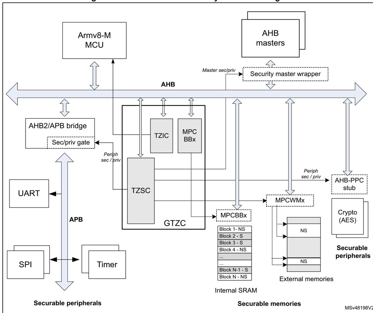
5.2.1 GTZC TrustZone system architecture
The Armv8-M supports security per TrustZone-M model with isolation between:
- • a secure world, where usually security sensitive applications are run and critical resources are located; secure transactions are signaled with HNONSEC[1] = 0 on AHB bus
- • a non-secure or public world (such as usual non secure and user space) where non-secure transactions are signaled with HNONSEC = 1 on AHB bus
The TrustZone architecture is extended beyond AHB and Armv8-M with:
- • AHB/APB bridge used as secure gate to block or propagate secure/non-secure and privilege/non-privilege transaction towards APB agents
- • peripheral protection controller (PPC) used as secure gate to block or propagate secure/non-secure and privilege/non-privilege transaction towards AHB agents
- • TrustZone block-based MPC firewalls used as secure gate to filter secure/non secure access towards internal SRAMs
- • Trustzone watermark MPC firewalls used as secure gate to filter secure/non secure access towards external memories
AHB and APB peripherals can be categorized as:
- • privilege: peripherals protected by AHB/APB firewall stub that is controlled from TZSC to define privilege properties
- • secure: peripherals always protected by an AHB/APB firewall stub. These peripherals are always secure (TZIC).
- • securable: peripherals protected by an AHB/APB firewall stub that is controlled from TZSC to define security properties (optional)
- • non-secure and non-privilege: peripherals connected directly to AHB/APB interconnect without any secure gate
- • TrustZone-aware: peripherals connected directly to AHB or APB bus and implementing a specific TrustZone behavior (such as a subset of registers being secure). TrustZone-aware AHB masters always drive HNONSEC signal according to their security mode (such as Armv8-M core or DMA).
AHB securable masters can be configured in the TZSC to be secure/non-secure and/or privilege/non-privilege.
Application information
The TZSC, MPCBB and TZIC sub-blocks can be used in one of the following ways:
- • programmed during secure Boot only, locked and not changed afterwards
- • dynamically re-programmed when using specific application code or secure kernel (microvisor). When not locked, MPC secure blocks or region size can be changed by secure software executing from the secure FLASH memory region or secure SRAM. Same remark applies to the GTZC_TZSC_SECCFRGx and GTZC_TZSC_PRIVCFGRx registers that define secure/privilege state of each peripheral.
The Armv8-M security architecture with secure, securable and TrustZone-aware peripherals is shown in Figure 14.
Figure 14. GTZC in Armv8-M subsystem block diagram
5.3 GTZC functional description
5.3.1 GTZC block diagram
Figure 15 describes the combined feature of TZSC, MPCBB and TZIC. Each sub-block is controlled by its own AHB configuration port. The TZSC defines which peripheral is secured and/or privileged.
The privilege configuration bit of a given peripheral can be modified by a secure-privilege transaction when the peripheral has been configured as secure, otherwise a privileged transaction (non-secure) is sufficient. The definition of these privilege attributes is possible even when TZEN = 0.
The secure configuration bit a given peripheral can be modified only with a secure-privilege transaction if the peripheral has been configured as privilege, otherwise a secure transaction (non-privileged) is sufficient.
Figure 15. GTZC block diagram
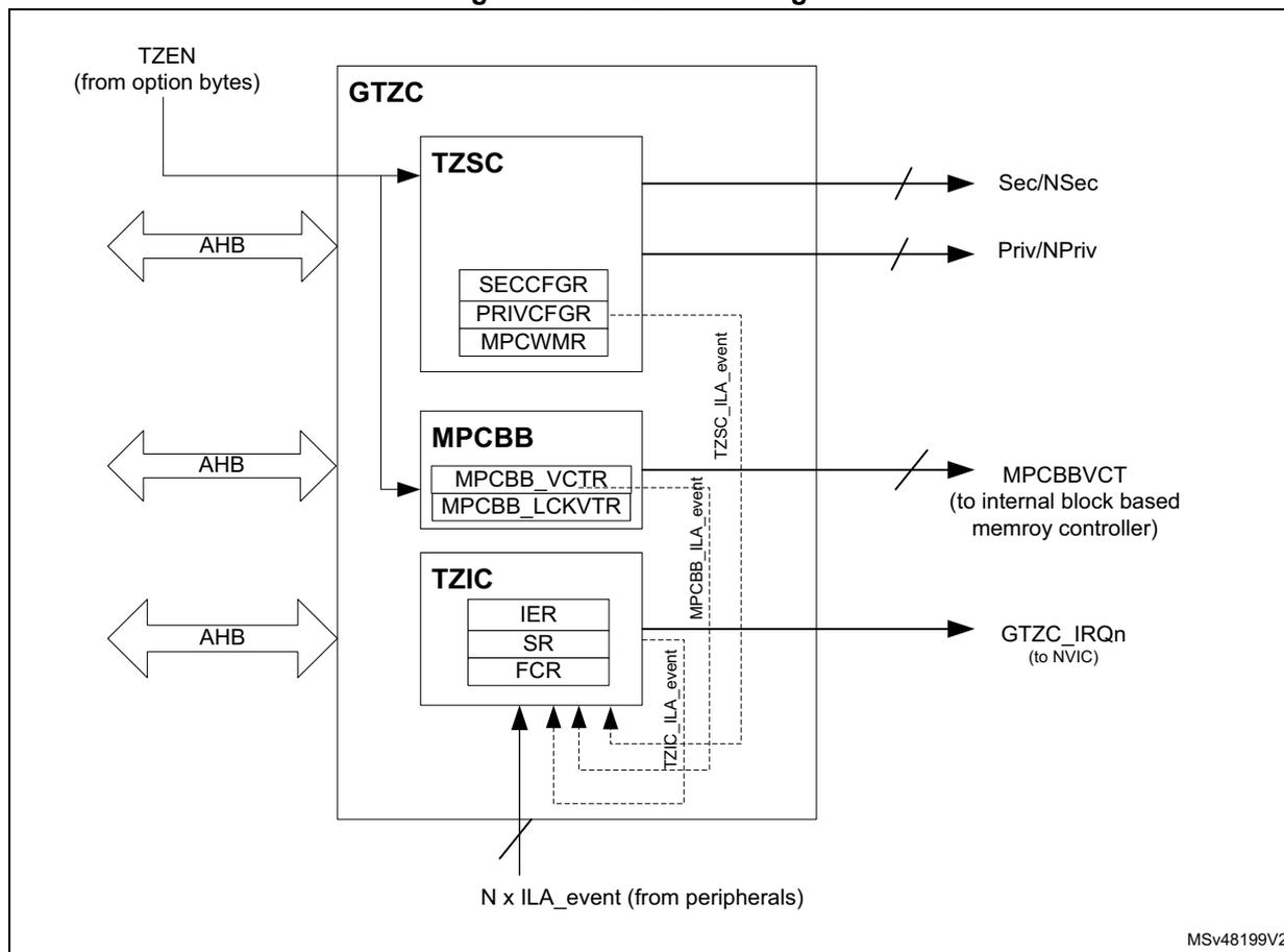
MSV48199V2
5.3.2 Illegal access definition
Three different types of illegal access exist:
- • Illegal non-secure access
Any non-secure transaction trying to write a secure resource is considered as illegal and thus the addressed resource generates an illegal access event for illegal write access, and a bus error for illegal fetch access. However some exceptions exist on transactions to secure and privilege configuration registers; these later ones authorized non-secure read access to secure registers (see GTZC_TZSC_SECCFGRx and GTZC_TZSC_PRIVCFGRx registers).
- • Illegal secure access
Any secure transaction trying to access a non-secure block in internal block-based SRAM or watermarked external memory, is considered as illegal.
Correct settings of the TZIC allows the capture of the associated event and then generates the GTZC_IRQn interrupt to the NVIC. This applies for read, write and execute access.
Concerning the MPCBB controller, there is an option to ignore secure data read/write access on non-secure SRAM blocks, by setting the SRWILADIS configuration bit in the GTZC_MPCBBx_CR register. Secure read and write data transactions are then allowed on non-secure SRAM blocks, while secure execution access remains not allowed.
Any secure execute transaction trying to access a non-secure peripheral register or memory is considered as illegal and generates a bus error.
- • Illegal non-privilege access
Any non-privilege transaction trying to access a privilege resource is considered as illegal. There is no illegal access event generated for this type of illegal access. The addressed resource follows a silent-fail behavior, returning all zero data for read and ignoring any write. No bus error is generated.
5.3.3 TrustZone security controller (TZSC)
This block is composed of a configurable set of registers, providing the following features:
- • Control of secure and privilege state for all peripherals, done through:
- – GTZC_TZSC_SECCFGRx registers to control AHB/APB firewall stubs for the securable peripherals and/or master
- – GTZC_TZSC_PRIVCFGRx registers to control AHB/APB firewall stubs for the privileged peripherals and/or master
- • For watermark memory protection controller (external memories), two independent regions can be defined and the following fields are used to program:
- – start of the first non-secure area on external memory = NSWMxSTRT1[10:0]
- – length of the first non-secure area on external memory = NSWMxLGTH1[11:0]
- – start of the second non-secure area on external memory = NSWMxSTRT2[10:0]
- – length of the second non-secure area on external memory = NSWMxLGTH2[11:0]
Note: x represents the target external memory interface (such as FMC or OCTOSPI). The total area considered as non-secure is the sum of the two independent ones. An overlap of one section over the other one has no specific effect.
Table 24 describes the characteristics of the available MPCWMx.
Table 24. MPCWMx
| MPC | Type | Number of regions | Target memory interface |
|---|---|---|---|
| MPCWM1 | Non secure watermark (region) | 2 | OCTOSPI |
| MPCWM2 | Non secure watermark (region) | 2 | FMC_NOR bank |
| MPCWM3 | Non secure watermark (region) | 1 | FMC_NAND bank |
5.3.4 Memory protection controller - block based (MPCBB)
For block-based memory protection controller (internal SRAM), the below registers are available:
- • GTZC_MPCBBx_VCTRY to program the vector defining 32 consecutive 256-byte block states, secure or non-secure (means y registers of 32 bits)
- • GTZC_MPCBBx_LCKVTRY to program the lock of super block (32 blocks)
Note: y represents the number of super-blocks (super-block = 32 blocks of SRAM_BB_size). On the STM32L552xx and STM32L562xx devices, the SRAM size = 192 Kbytes and the block size = 256 bytes, then super-block size = 32 * 256 = 8 Kbytes and y = 192 / 8 = 24. It means 24 vector registers (32-bit) are needed to control the secure state of all the 256-byte blocks. Concerning the lock bit, only one 32-bit lock register is needed since a single lock bit applies on a super-block (32 * 256 bytes).
Table 25 describes the characteristics of the available MPCBBx.
Table 25. MPCBBx
| MPC | Type | Number of blocks | Target memory interface |
|---|---|---|---|
| MPCBB1 | Block based (block size = 256 bytes) | 768 | SRAM1 |
| MPCBB2 | Block based (block size = 256 bytes) | 256 | SRAM2 |
5.3.5 TrustZone illegal access controller (TZIC)
This block concentrates all illegal access source events. It is used only when the system is TrustZone enabled (TZEN = 1).
TZIC allows the trace of which event triggered the NVIC GTZC_IRQn. Register masks (GTZC_TZIC_IERx) are available to filter unwanted event. On unmasked illegal event, the TZIC generates the GTZC_IRQn signal to NVIC that corresponds to the GTZC_IRQn secure interrupt.
For each illegal event source, a status flag and a clear bit exist (respectively within GTZC_TZIC_SRx and GTZC_TZIC_FCRx registers). The reset value of mask registers (GTZC_TZIC_IERx) is such that all events are masked.
5.3.6 Power-on/reset state
The power-on and reset state of the TZSC clear all bits of GTZC_TZSC_SECCFGRx and GTZC_TZSC_PRIVCFGRx registers to 0, which respectively means non-secure and non-privilege. Concerning the internal SRAM, the reset values of the GTZC_MPCBBx_VCTRY registers are set to 0xFFFF FFFF, making all blocks of the block-based SRAM memory secure. This is valid only when TrustZone security is enabled at system level (TZEN = 1). In the other case (legacy mode, TZEN = 0), the reset values of the GTZC_MPCBBx_VCTRY registers are set to 0x0000 0000 so that all block-based SRAM memories are non-secure.
Same thing applies for external memories, all MPCWMx_NSWMyR registers must be set to 0xFFFF FFFF, making the whole external memory non-secure. Secure Boot code can then program the security settings, making components secure or not as needed.
5.3.7 DMA requests
TZSC does not support any DMA interface.
5.4 GTZC events
MPCBB and TZIC are secure peripherals, thus they both systematically generate an illegal access event when accessed by a non-secure access. The TZSC is a TrustZone-aware peripheral, meaning that secure and non-secure registers co-exist within the peripheral. An
exception exists for the GTZC_TZSC_SECCFGR and GTZC_TZSC_PRIVCGFR: any read access, secure or not, are supported.
5.5 GTZC_TZSC registers
All registers are accessed only by words (32-bit).
5.5.1 GTZC_TZSC control register (GTZC_TZSC_CR)
Address offset: 0x000
Reset value: 0x0000 0000
Write-secure access only.
Read accesses are authorized for any type of transactions, secure or not, privilege or not.
| 31 | 30 | 29 | 28 | 27 | 26 | 25 | 24 | 23 | 22 | 21 | 20 | 19 | 18 | 17 | 16 |
|---|---|---|---|---|---|---|---|---|---|---|---|---|---|---|---|
| Res. | Res. | Res. | Res. | Res. | Res. | Res. | Res. | Res. | Res. | Res. | Res. | Res. | Res. | Res. | Res. |
| 15 | 14 | 13 | 12 | 11 | 10 | 9 | 8 | 7 | 6 | 5 | 4 | 3 | 2 | 1 | 0 |
| Res. | Res. | Res. | Res. | Res. | Res. | Res. | Res. | Res. | Res. | Res. | Res. | Res. | Res. | Res. | LCK |
| rw |
Bits 31:1 Reserved, must be kept at reset value.
Bit 0 LCK : lock the configuration of TZSC items until next reset
This bit is unset by default and once set, it can not be reset until global TZSC reset.
0: control register not locked
1: control register locked
5.5.2 GTZC_TZSC secure configuration register 1 (GTZC_TZSC_SECCFGR1)
Address offset: 0x010
Reset value: 0x0000 0000
Write-secure access only.
This register can be written only by privilege secure transaction when corresponding TZSC_PRIVCFGR register signal is set to 1. If a given PRIV bit is not set, the equivalent SEC bit can be written by non- privilege secure transaction.
Read accesses are authorized for any type of transactions, secure or not, privilege or not.
| 31 | 30 | 29 | 28 | 27 | 26 | 25 | 24 | 23 | 22 | 21 | 20 | 19 | 18 | 17 | 16 |
|---|---|---|---|---|---|---|---|---|---|---|---|---|---|---|---|
| SPI1SEC | TIM1SEC | COMPSEC | VREFBUFSEC | UCPD1SEC | USBFSSEC | FDCAN1SEC | LPTIM3SEC | LPTIM2SEC | I2C4SEC | LPUART1SEC | LPTIM1SEC | OPAMPSEC | DAC1SEC | CRSSEC | I2C3SEC |
| rw | rw | rw | rw | rw | rw | rw | rw | rw | rw | rw | rw | rw | rw | rw | rw |
| 15 | 14 | 13 | 12 | 11 | 10 | 9 | 8 | 7 | 6 | 5 | 4 | 3 | 2 | 1 | 0 |
| I2C2SEC | I2C1SEC | UART5SEC | UART4SEC | USART3SEC | USART2SEC | SPI3SEC | SPI2SEC | IWDGSEC | WWDGSEC | TIM7SEC | TIM6SEC | TIM5SEC | TIM4SEC | TIM3SEC | TIM2SEC |
| rw | rw | rw | rw | rw | rw | rw | rw | rw | rw | rw | rw | rw | rw | rw | rw |
Bit 31 SPI1SEC : secure access mode for SPI1
0: non-secure
1: secure
Bit 30 TIM1SEC : secure access mode for TIM1
0: non-secure
1: secure
Bit 29 COMPSEC : secure access mode for COMP
0: non-secure
1: secure
Bit 28 VREFBUFSEC : secure access mode for VREFBUF
0: non-secure
1: secure
Bit 27 UCPD1SEC : secure access mode for UCPD1
0: non-secure
1: secure
Bit 26 USBFSSEC : secure access mode for USB FS
0: non-secure
1: secure
Bit 25 FDCAN1SEC : secure access mode for FDCAN1
0: non-secure
1: secure
- Bit 24
LPTIM3SEC
: secure access mode for LPTIM3
0: non-secure
1: secure - Bit 23
LPTIM2SEC
: secure access mode for LPTIM2
0: non-secure
1: secure - Bit 22
I2C4SEC
: secure access mode for I2C4
0: non-secure
1: secure - Bit 21
LPUART1SEC
: secure access mode for LPUART1
0: non-secure
1: secure - Bit 20
LPTIM1SEC
: secure access mode for LPTIM1
0: non-secure
1: secure - Bit 19
OPAMPSEC
: secure access mode for OPAMP
0: non-secure
1: secure - Bit 18
DAC1SEC
: secure access mode for DAC1
0: non-secure
1: secure - Bit 17
CRSSEC
: secure access mode for CRS
0: non-secure
1: secure - Bit 16
I2C3SEC
: secure access mode for I2C3
0: non-secure
1: secure - Bit 15
I2C2SEC
: secure access mode for I2C2
0: non-secure
1: secure - Bit 14
I2C1SEC
: secure access mode for I2C1
0: non-secure
1: secure - Bit 13
UART5SEC
: secure access mode for UART5
0: non-secure
1: secure - Bit 12
UART4SEC
: secure access mode for UART4
0: non-secure
1: secure - Bit 11
USART3SEC
: secure access mode for USART3
0: non-secure
1: secure - Bit 10
USART2SEC
: secure access mode for USART2
0: non-secure
1: secure
- Bit 9
SPI3SEC
: secure access mode for SPI3
0: non-secure
1: secure - Bit 8
SPI2SEC
: secure access mode for SPI2
0: non-secure
1: secure - Bit 7
IWDGSEC
: secure access mode for IWDG
0: non-secure
1: secure - Bit 6
WWDGSEC
: secure access mode for WWDG
0: non-secure
1: secure - Bit 5
TIM7SEC
: secure access mode for TIM7
0: non-secure
1: secure - Bit 4
TIM6SEC
: secure access mode for TIM6
0: non-secure
1: secure - Bit 3
TIM5SEC
: secure access mode for TIM5
0: non-secure
1: secure - Bit 2
TIM4SEC
: secure access mode for TIM4
0: non-secure
1: secure - Bit 1
TIM3SEC
: secure access mode for TIM3
0: non-secure
1: secure - Bit 0
TIM2SEC
: secure access mode for TIM2
0: non-secure
1: secure
5.5.3 GTZC_TZSC secure configuration register 2 (GTZC_TZSC_SECCFGR2)
Address offset: 0x014
Reset value: 0x0000 0000
Write-secure access only.
This register can be written only by privilege secure transaction when corresponding TZSC_PRIVCFGR register signal is set to 1. If a given PRIV is not set, the equivalent SEC bit can be written by non- privilege secure transaction.
Read accesses are authorized for any type of transactions, secure or not, privilege or not.
| 31 | 30 | 29 | 28 | 27 | 26 | 25 | 24 | 23 | 22 | 21 | 20 | 19 | 18 | 17 | 16 |
|---|---|---|---|---|---|---|---|---|---|---|---|---|---|---|---|
| Res. | Res. | Res. | Res. | Res. | Res. | Res. | Res. | Res. | Res. | Res. | Res. | Res. | OCTOSPI1_REGSEC | FMC_REGSEC | SDMMC1SEC |
| rw | rw | rw | |||||||||||||
| 15 | 14 | 13 | 12 | 11 | 10 | 9 | 8 | 7 | 6 | 5 | 4 | 3 | 2 | 1 | 0 |
| PKASEC | RNGSEC | HASHSEC | AESSEC | ADCSEC | ICACHE_REGSEC | TSCSEC | CRCSEC | DFSDM1SEC | SAI2SEC | SAI1SEC | TIM17SEC | TIM16SEC | TIM15SEC | USART1SEC | TIM8SEC |
| rw | rw | rw | rw | rw | rw | rw | rw | rw | rw | rw | rw | rw | rw | rw | rw |
Bits 31:19 Reserved, must be kept at reset value.
Bit 18 OCTOSPI1_REGSEC : secure access mode for OCTOSPI1 registers
0: non-secure
1: secure
Bit 17 FMC_REGSEC : secure access mode for FMC registers
0: non-secure
1: secure
Bit 16 SDMMC1SEC : secure access mode for SDMMC1
0: non-secure
1: secure
Bit 15 PKASEC : secure access mode for PKA
0: non-secure
1: secure
Bit 14 RNGSEC : secure access mode for RNG
0: non-secure
1: secure
Bit 13 HASHSEC : secure access mode for HASH
0: non-secure
1: secure
- Bit 12
AESSEC
: secure access mode for AES
0: non-secure
1: secure - Bit 11
ADCSEC
: secure access mode for ADC
0: non-secure
1: secure - Bit 10
ICACHE_REGSEC
: secure access mode for ICACHE registers
0: non-secure
1: secure - Bit 9
TSCSEC
: secure access mode for TSC
0: non-secure
1: secure - Bit 8
CRCSEC
: secure access mode for CRC
0: non-secure
1: secure - Bit 7
DFSDM1SEC
: secure access mode for DFSDM1
0: non-secure
1: secure - Bit 6
SAI2SEC
: secure access mode for SAI2
0: non-secure
1: secure - Bit 5
SAI1SEC
: secure access mode for SAI1
0: non-secure
1: secure - Bit 4
TIM17SEC
: secure access mode for TIM17
0: non-secure
1: secure - Bit 3
TIM16SEC
: secure access mode for TIM16
0: non-secure
1: secure - Bit 2
TIM15SEC
: secure access mode for TIM15
0: non-secure
1: secure - Bit 1
USART1SEC
: secure access mode for USART1
0: non-secure
1: secure - Bit 0
TIM8SEC
: secure access mode for TIM8
0: non-secure
1: secure
5.5.4 GTZC_TZSC privilege configuration register 1 (GTZC_TZSC_PRIVCFGR1)
Address offset: 0x020
Reset value: 0x0000 0000
Write-privileged access only.
This register can be read or written only by secure privilege transaction when corresponding TZSC_SECCFGR register signal is set to 1. If a given SEC bit is not set, the equivalent PRIV bit can be read/written by non-secure privileged transaction.
Read accesses are authorized for any type of transactions, secure or not, privilege or not.
| 31 | 30 | 29 | 28 | 27 | 26 | 25 | 24 | 23 | 22 | 21 | 20 | 19 | 18 | 17 | 16 |
|---|---|---|---|---|---|---|---|---|---|---|---|---|---|---|---|
| SPI1PRIV | TIM1PRIV | COMPPRIV | VREFBUFPRIV | UCPD1PRIV | USBFSPRIV | FDCAN1PRIV | LPTIM3PRIV | LPTIM2PRIV | I2C4PRIV | LPUART1PRIV | LPTIM1PRIV | OPAMPPRIV | DAC1PRIV | CRSPRIV | I2C3PRIV |
| r/w | r/w | r/w | r/w | r/w | r/w | r/w | r/w | r/w | r/w | r/w | r/w | r/w | r/w | r/w | r/w |
| 15 | 14 | 13 | 12 | 11 | 10 | 9 | 8 | 7 | 6 | 5 | 4 | 3 | 2 | 1 | 0 |
| I2C2PRIV | I2C1PRIV | UART5PRIV | UART4PRIV | USART3PRIV | USART2PRIV | SPI3PRIV | SPI2PRIV | IWDGPRIV | WWDGPRIV | TIM7PRIV | TIM6PRIV | TIM5PRIV | TIM4PRIV | TIM3PRIV | TIM2PRIV |
| r/w | r/w | r/w | r/w | r/w | r/w | r/w | r/w | r/w | r/w | r/w | r/w | r/w | r/w | r/w | r/w |
Bit 31 SPI1PRIV : privilege access mode for SPI1
0: non-privilege
1: privilege
Bit 30 TIM1PRIV : privilege access mode for TIM1
0: non-privilege
1: privilege
Bit 29 COMPPRIV : privilege access mode for COMP
0: non-privilege
1: privilege
Bit 28 VREFBUFPRIV : privilege access mode for VREFBUF
0: non-privilege
1: privilege
Bit 27 UCPD1PRIV : privilege access mode for UCPD1
0: non-privilege
1: privilege
Bit 26 USBFSPRIV : privilege access mode for USB FS
0: non-privilege
1: privilege
Bit 25 FDCAN1PRIV : privilege access mode for FDCAN1
0: non-privilege
1: privilege
- Bit 24
LPTIM3PRIV
: privilege access mode for LPTIM3
0: non-privilege
1: privilege - Bit 23
LPTIM2PRIV
: privilege access mode for LPTIM2
0: non-privilege
1: privilege - Bit 22
I2C4PRIV
: privilege access mode for I2C4
0: non-privilege
1: privilege - Bit 21
LPUART1PRIV
: privilege access mode for LPUART1
0: non-privilege
1: privilege - Bit 20
LPTIM1PRIV
: privilege access mode for LPTIM1
0: non-privilege
1: privilege - Bit 19
OPAMPPRIV
: privilege access mode for OPAMP
0: non-privilege
1: privilege - Bit 18
DAC1PRIV
: privilege access mode for DAC1
0: non-privilege
1: privilege - Bit 17
CRSPRIV
: privilege access mode for CRS
0: non-privilege
1: privilege - Bit 16
I2C3PRIV
: privilege access mode for I2C3
0: non-privilege
1: privilege - Bit 15
I2C2PRIV
: privilege access mode for I2C2
0: non-privilege
1: privilege - Bit 14
I2C1PRIV
: privilege access mode for I2C1
0: non-privilege
1: privilege - Bit 13
UART5PRIV
: privilege access mode for UART5
0: non-privilege
1: privilege - Bit 12
UART4PRIV
: privilege access mode for UART4
0: non-privilege
1: privilege - Bit 11
USART3PRIV
: privilege access mode for USART3
0: non-privilege
1: privilege - Bit 10
USART2PRIV
: privilege access mode for USART2
0: non-privilege
1: privilege
- Bit 9
SPI3PRIV
: privilege access mode for SPI3
0: non-privilege
1: privilege - Bit 8
SPI2PRIV
: privilege access mode for SPI2
0: non-privilege
1: privilege - Bit 7
IWDGPRIV
: privilege access mode for IWDG
0: non-privilege
1: privilege - Bit 6
WWDGPRIV
: privilege access mode for WWDG
0: non-privilege
1: privilege - Bit 5
TIM7PRIV
: privilege access mode for TIM7
0: non-privilege
1: privilege - Bit 4
TIM6PRIV
: privilege access mode for TIM6
0: non-privilege
1: privilege - Bit 3
TIM5PRIV
: privilege access mode for TIM5
0: non-privilege
1: privilege - Bit 2
TIM4PRIV
: privilege access mode for TIM4
0: non-privilege
1: privilege - Bit 1
TIM3PRIV
: privilege access mode for TIM3
0: non-privilege
1: privilege - Bit 0
TIM2PRIV
: privilege access mode for TIM2
0: non-privilege
1: privilege
5.5.5 GTZC_TZSC privilege configuration register 2 (GTZC_TZSC_PRIVCFGR2)
Address offset: 0x024
Reset value: 0x0000 0000
Write-privileged access only.
This register can be read or written only by secure privilege transaction when corresponding TZSC_SECCFGR register signal is set to 1. If a given SEC bit is not set, the equivalent PRIV bit can be read/written by non-secure privileged transaction.
Read accesses are authorized for any type of transactions, secure or not, privilege or not.
| 31 | 30 | 29 | 28 | 27 | 26 | 25 | 24 | 23 | 22 | 21 | 20 | 19 | 18 | 17 | 16 |
|---|---|---|---|---|---|---|---|---|---|---|---|---|---|---|---|
| Res. | Res. | Res. | Res. | Res. | Res. | Res. | Res. | Res. | Res. | Res. | Res. | Res. | OCTOSPI1_REGPRIV | FMC_REGPRIV | SDMMC1PRIV |
| rw | rw | rw | |||||||||||||
| 15 | 14 | 13 | 12 | 11 | 10 | 9 | 8 | 7 | 6 | 5 | 4 | 3 | 2 | 1 | 0 |
| PKAPRIV | RNGPRIV | HASHPRIV | AESPRIV | ADCPRIV | ICACHE_REGPRIV | TSCPRIV | CRCPRIV | DFSDM1PRIV | SAI2PRIV | SAI1PRIV | TIM17PRIV | TIM16PRIV | TIM15PRIV | USART1PRIV | TIM8PRIV |
| rw | rw | rw | rw | rw | rw | rw | rw | rw | rw | rw | rw | rw | rw | rw | rw |
Bits 31:19 Reserved, must be kept at reset value.
Bit 18 OCTOSPI1_REGPRIV : privilege access mode for OCTOSPI1 registers
0: non-privilege
1: privilege
Bit 17 FMC_REGPRIV : privilege access mode for FMC registers
0: non-privilege
1: privilege
Bit 16 SDMMC1PRIV : privilege access mode for SDMMC1
0: non-privilege
1: privilege
Bit 15 PKAPRIV : privilege access mode for PKA
0: non-privilege
1: privilege
Bit 14 RNGPRIV : privilege access mode for RNG
0: non-privilege
1: privilege
Bit 13 HASHPRIV : privilege access mode for HASH
0: non-privilege
1: privilege
- Bit 12
AESPRIV
: privilege access mode for AES
0: non-privilege
1: privilege - Bit 11
ADCPRIV
: privilege access mode for ADC
0: non-privilege
1: privilege - Bit 10
ICACHE_REGPRIV
: privilege access mode for ICACHE registers
0: non-privilege
1: privilege - Bit 9
TSCPRIV
: privilege access mode for TSC
0: non-privilege
1: privilege - Bit 8
CRCPRI
: privilege access mode for CRC
0: non-privilege
1: privilege - Bit 7
DFSDM1PRIV
: privilege access mode for DFSDM1
0: non-privilege
1: privilege - Bit 6
SAI2PRIV
: privilege access mode for SAI2
0: non-privilege
1: privilege - Bit 5
SAI1PRIV
: privilege access mode for SAI1
0: non-privilege
1: privilege - Bit 4
TIM17PRIV
: privilege access mode for TIM17
0: non-privilege
1: privilege - Bit 3
TIM16PRIV
: privilege access mode for TIM16
0: non-privilege
1: privilege - Bit 2
TIM15PRIV
: privilege access mode for TIM15
0: non-privilege
1: privilege - Bit 1
USART1PRIV
: privilege access mode for USART1
0: non-privilege
1: privilege - Bit 0
TIM8PRIV
: privilege access mode for TIM8
0: non-privilege
1: privilege
5.5.6 GTZC_TZSC external memory x non-secure watermark register 1 (GTZC_TZSC_MPCWMxANSR)
Address offset: 0x030 + 0x008 * (x-1), (x = 1 to 3)
Reset value: 0x0000 0000
The given reset value is valid when TZEN = 1. The reset value is 0x0800 0000 when TZEN = 0.
Secure access only.
Caution: When NSWM1STRT + NSWM1LGTH is higher than the maximum size allowed for the memory, a saturation of NSWM1LGTH is applied automatically.
| 31 | 30 | 29 | 28 | 27 | 26 | 25 | 24 | 23 | 22 | 21 | 20 | 19 | 18 | 17 | 16 |
|---|---|---|---|---|---|---|---|---|---|---|---|---|---|---|---|
| Res. | Res. | Res. | Res. | NSWM1LGTH[11:0] | |||||||||||
| rw | rw | rw | rw | rw | rw | rw | rw | rw | rw | rw | rw | ||||
| 15 | 14 | 13 | 12 | 11 | 10 | 9 | 8 | 7 | 6 | 5 | 4 | 3 | 2 | 1 | 0 |
| Res. | Res. | Res. | Res. | Res. | NSWM1STRT[10:0] | ||||||||||
| rw | rw | rw | rw | rw | rw | rw | rw | rw | rw | rw | |||||
Bits 31:28 Reserved, must be kept at reset value.
Bits 27:16 NSWM1LGTH[11:0] : length of the first non-secure area (multiple of 128 Kbytes)
Note: If programmed NSWM1LGTH + NSWM1STRT is over 2048, the value stored in the register is truncated to (0x800 - NSWM1STRT). Any subsequent read returns this value.
Bits 15:11 Reserved, must be kept at reset value.
Bits 10:0 NSWM1STRT[10:0] : offset address for the first non-secure area (multiple of 128 Kbytes)
Note: External memories which are watermark controlled start fully non-secure at reset when TZEN = 0. When TZEN = 1, external memories start fully secure (inverted reset-value).
5.5.7 GTZC_TZSC external memory x non-secure watermark register 2 (GTZC_TZSC_MPCWMxBNSR)
Address offset: 0x034 + 0x008 * (x-1), (x = 1 to 2)
Reset value: 0x0000 0000
The given reset value is valid when TZEN = 1. The reset value is 0x0800 0000 when TZEN = 0.
Secure access only.
Caution: When NSWM1STRT + NSWM1LGTH is higher than the maximum size allowed for the memory, a saturation of NSWM1LGTH is applied automatically.
Note: If NSWM1LGTH = 0, the region 1 is disabled and the only non-secure memory space is defined by NSWMPxWM2.
If both NSWMPxWM1 and NSWMPxWM2 have the reset value 0x0000 0000, all the memory space of the external memory x (FMC NOR/SRAM or OCTOSPI) is secure.
If NSWM1LGTH = 0x800 and NSWM1STRT = 0, the whole 256-Mbyte memory space is non-secure (independent of NSWMPxWM2 value).
If NSWM1LGTH = 0x001 and NSWM1STRT = 0x7FF, only one 128-Kbyte block is defined as non-secure (at address offset = 0x0FFE 0000, ending at 0x0FFF FFFF).
| 31 | 30 | 29 | 28 | 27 | 26 | 25 | 24 | 23 | 22 | 21 | 20 | 19 | 18 | 17 | 16 |
|---|---|---|---|---|---|---|---|---|---|---|---|---|---|---|---|
| Res. | Res. | Res. | Res. | NSWM2LGTH[11:0] | |||||||||||
| rw | rw | rw | rw | rw | rw | rw | rw | rw | rw | rw | rw | ||||
| 15 | 14 | 13 | 12 | 11 | 10 | 9 | 8 | 7 | 6 | 5 | 4 | 3 | 2 | 1 | 0 |
| Res. | Res. | Res. | Res. | Res. | NSWM2STRT[10:0] | ||||||||||
| rw | rw | rw | rw | rw | rw | rw | rw | rw | rw | rw | |||||
Bits 31:28 Reserved, must be kept at reset value.
Bits 27:16 NSWM2LGTH[11:0] : length of the second non-secure area (multiple of 128 Kbytes)
Note: If programmed NSWM2LGTH + NSWM2STRT is over 2048, the value stored in the register is truncated to (0x800 - NSWM2STRT). Any subsequent read returns this value.
Bits 15:11 Reserved, must be kept at reset value.
Bits 10:0 NSWM2STRT[10:0] : offset address for the second non-secure area (multiple of 128 Kbytes)
Note: External memories which are watermark controlled start fully non-secure at reset when TZEN = 0. When TZEN = 1, external memories start fully secure (inverted reset-value).
5.5.8 GTZC_TZSC register map and reset values
Table 26. GTZC_TZSC register map and reset values
| Offset | Register | 31 | 30 | 29 | 28 | 27 | 26 | 25 | 24 | 23 | 22 | 21 | 20 | 19 | 18 | 17 | 16 | 15 | 14 | 13 | 12 | 11 | 10 | 9 | 8 | 7 | 6 | 5 | 4 | 3 | 2 | 1 | 0 |
|---|---|---|---|---|---|---|---|---|---|---|---|---|---|---|---|---|---|---|---|---|---|---|---|---|---|---|---|---|---|---|---|---|---|
| 0x000 | GTZC_TZSC_CR | Res. | Res. | Res. | Res. | Res. | Res. | Res. | Res. | Res. | Res. | Res. | Res. | Res. | Res. | Res. | Res. | Res. | Res. | Res. | Res. | Res. | Res. | Res. | Res. | Res. | Res. | Res. | Res. | Res. | Res. | Res. | ILCK |
| Reset value | 0 | ||||||||||||||||||||||||||||||||
| 0x004 to 0x00C | Reserved | Reserved | |||||||||||||||||||||||||||||||
| 0x010 | GTZC_TZSC_SECCFG1 | SP11SEC | TIM11SEC | COMPSEC | VREFBUFSEC | UOPD1SEC | USBFSSSEC | FDCAN1SEC | LPTIM3SEC | LPTIM2SEC | I2C4SEC | LPUART1SEC | LPTIM1SEC | OPAMPSEC | DAC1SEC | CRSSEC | I2C3SEC | I2C2SEC | I2C1SEC | UART5SEC | UART4SEC | USART3SEC | USART2SEC | SPI3SEC | SPI2SEC | IWDGSEC | WWDGSEC | TIM7SEC | TIM6SEC | TIM5SEC | TIM4SEC | TIM3SEC | TIM2SEC |
| Reset value | 0 | 0 | 0 | 0 | 0 | 0 | 0 | 0 | 0 | 0 | 0 | 0 | 0 | 0 | 0 | 0 | 0 | 0 | 0 | 0 | 0 | 0 | 0 | 0 | 0 | 0 | 0 | 0 | 0 | 0 | 0 | ||
| 0x014 | GTZC_TZSC_SECCFG2 | Res. | Res. | Res. | Res. | Res. | Res. | Res. | Res. | Res. | Res. | Res. | Res. | Res. | OCTOSPI1_REGSEC | FMC_REGSEC | SDMMC1SEC | PKASEC | RNGSEC | HASHSEC | AESSEC | ADCSEC | ICACHE_REGSEC | TSCSEC | CRCSEC | DFSDM1SEC | SAI2SEC | SAI1SEC | TIM17SEC | TIM16SEC | TIM15SEC | USART1SEC | TIM8SEC |
| Reset value | 0 | 0 | 0 | 0 | 0 | 0 | 0 | 0 | 0 | 0 | 0 | 0 | 0 | 0 | 0 | 0 | 0 | 0 | |||||||||||||||
| 0x018 to 0x01C | Reserved | Reserved | |||||||||||||||||||||||||||||||
Table 26. GTZC_TZSC register map and reset values (continued)
| Offset | Register | 31 | 30 | 29 | 28 | 27 | 26 | 25 | 24 | 23 | 22 | 21 | 20 | 19 | 18 | 17 | 16 | 15 | 14 | 13 | 12 | 11 | 10 | 9 | 8 | 7 | 6 | 5 | 4 | 3 | 2 | 1 | 0 |
|---|---|---|---|---|---|---|---|---|---|---|---|---|---|---|---|---|---|---|---|---|---|---|---|---|---|---|---|---|---|---|---|---|---|
| 0x020 | GTZC_TZSC _PRIVCFG1 | SPI1PRIV | TIM1PRIV | COMP1PRIV | VREFBUFP1PRIV | UCPD1PRIV | USBFSPIPRIV | FDCAN1PRIV | LPTIM3PRIV | LPTIM2PRIV | I2C4PRIV | LPUART1PRIV | LPTIM1PRIV | OPAMP1PRIV | DAC1PRIV | CRS1PRIV | I2C3PRIV | I2C2PRIV | I2C1PRIV | UART5PRIV | UART4PRIV | USART3PRIV | USART2PRIV | SPI3PRIV | SPI2PRIV | IWDGPRIV | WWDGPRIV | TIM7PRIV | TIM6PRIV | TIM5PRIV | TIM4PRIV | TIM3PRIV | TIM2PRIV |
| Reset value | 0 | 0 | 0 | 0 | 0 | 0 | 0 | 0 | 0 | 0 | 0 | 0 | 0 | 0 | 0 | 0 | 0 | 0 | 0 | 0 | 0 | 0 | 0 | 0 | 0 | 0 | 0 | 0 | 0 | 0 | 0 | 0 | |
| 0x024 | GTZC_TZSC _PRIVCFG2 | Res | Res | Res | Res | Res | Res | Res | Res | Res | Res | Res | Res | Res | Res | OCTOSP1_REGPRIV | FMC_REGPRIV | SDMMC1PRIV | PKAPRIV | RNGPRIV | HASHPRIV | AESPRIV | ADCP1PRIV | ICACHE_REGPRIV | TSCPRIV | CRCP1PRIV | DFSDM1PRIV | SAI2PRIV | SAI1PRIV | TIM17PRIV | TIM16PRIV | TIM15PRIV | USART1PRIV |
| Reset value | 0 | 0 | 0 | 0 | 0 | 0 | 0 | 0 | 0 | 0 | 0 | 0 | 0 | 0 | 0 | 0 | 0 | ||||||||||||||||
| 0x028 to 0x02C | Reserved | Reserved | |||||||||||||||||||||||||||||||
| 0x030 | GTZC_TZSC _MPCWM1ANSR | Res | Res | Res | Res | NSWM1LGTH[11:0] | Res | Res | Res | Res | Res | NSWM1STR[10:0] | |||||||||||||||||||||
| Reset value | 0 | 0 | 0 | 0 | 0 | 0 | 0 | 0 | 0 | 0 | 0 | 0 | 0 | 0 | 0 | 0 | 0 | 0 | 0 | 0 | 0 | 0 | 0 | ||||||||||
| 0x034 | GTZC_TZSC _MPCWM1BNSR | Res | Res | Res | Res | NSWM2LGTH[11:0] | Res | Res | Res | Res | Res | NSWM2STR[10:0] | |||||||||||||||||||||
| Reset value | 0 | 0 | 0 | 0 | 0 | 0 | 0 | 0 | 0 | 0 | 0 | 0 | 0 | 0 | 0 | 0 | 0 | 0 | 0 | 0 | 0 | 0 | 0 | ||||||||||
| 0x038 | GTZC_TZSC _MPCWM2ANSR | Res | Res | Res | Res | NSWM1LGTH[11:0] | Res | Res | Res | Res | Res | NSWM1STR[10:0] | |||||||||||||||||||||
| Reset value | 0 | 0 | 0 | 0 | 0 | 0 | 0 | 0 | 0 | 0 | 0 | 0 | 0 | 0 | 0 | 0 | 0 | 0 | 0 | 0 | 0 | 0 | 0 | ||||||||||
| 0x03C | GTZC_TZSC _MPCWM2BNSR | Res | Res | Res | Res | NSWM2LGTH[11:0] | Res | Res | Res | Res | Res | NSWM2STR[10:0] | |||||||||||||||||||||
| Reset value | 0 | 0 | 0 | 0 | 0 | 0 | 0 | 0 | 0 | 0 | 0 | 0 | 0 | 0 | 0 | 0 | 0 | 0 | 0 | 0 | 0 | 0 | 0 | ||||||||||
| 0x040 | GTZC_TZSC _MPCWM3ANSR | Res | Res | Res | Res | NSWM1LGTH[11:0] | Res | Res | Res | Res | Res | NSWM1STR[10:0] | |||||||||||||||||||||
| Reset value | 0 | 0 | 0 | 0 | 0 | 0 | 0 | 0 | 0 | 0 | 0 | 0 | 0 | 0 | 0 | 0 | 0 | 0 | 0 | 0 | 0 | 0 | 0 | ||||||||||
5.6 GTZC_MPCBB registers
All registers are accessed only by words (32-bit).
5.6.1 GTZC_MPCBBx control register (GTZC_MPCBBx_CR) (x = 1 to 2)
Address offset: 0x800 + 0x400 * (x - 1)
Reset value: 0x0000 0000
Secure access only.
| 31 | 30 | 29 | 28 | 27 | 26 | 25 | 24 | 23 | 22 | 21 | 20 | 19 | 18 | 17 | 16 |
|---|---|---|---|---|---|---|---|---|---|---|---|---|---|---|---|
| SRWILADIS | INVSECSTATE | Res. | Res. | Res. | Res. | Res. | Res. | Res. | Res. | Res. | Res. | Res. | Res. | Res. | Res. |
| rw | rw | ||||||||||||||
| 15 | 14 | 13 | 12 | 11 | 10 | 9 | 8 | 7 | 6 | 5 | 4 | 3 | 2 | 1 | 0 |
| Res. | Res. | Res. | Res. | Res. | Res. | Res. | Res. | Res. | Res. | Res. | Res. | Res. | Res. | Res. | LCK |
| rw |
Bit 31 SRWILADIS: secure read/write illegal access disable
This bit disables the detection of an illegal access when a secure read/write transaction access a non-secure blocks of the block-based SRAM (secure fetch on non-secure block is always considered illegal).
0: enabled, secure read/write access not allowed on non-secure SRAM block
1: disabled, secure read/write access allowed on non-secure SRAM block
Bit 30 INVSECSTATE: default security state
This bit is used to invert the MPCBB status information (secure or non-secure) connected to the RCC, in order to define the MPCBB clock control as secure or not.
0: default state (source clock secured if a secure area exists in the MPCBB and vice-versa)
1: invert the state, source clock remains secure even if no secure block is set in the MPCBB
Bits 29:1 Reserved, must be kept at reset value.
Bit 0 LCK: lock the control register of the MPCBB sub-block until next reset
This bit is unset by default and once set, it can not be reset until global TZSC reset.
0: control register not locked
1: control register locked
5.6.2 GTZC_MPCBB1 lock register 1(GTZC_MPCBB1_LCKVTR1)
Address offset: 0x810
Reset value: 0x0000 0000
Secure access only.
| 31 | 30 | 29 | 28 | 27 | 26 | 25 | 24 | 23 | 22 | 21 | 20 | 19 | 18 | 17 | 16 |
|---|---|---|---|---|---|---|---|---|---|---|---|---|---|---|---|
| Res. | Res. | Res. | Res. | Res. | Res. | Res. | Res. | LCKSB23 | LCKSB22 | LCKSB21 | LCKSB20 | LCKSB19 | LCKSB18 | LCKSB17 | LCKSB16 |
| 15 | 14 | 13 | 12 | 11 | 10 | 9 | 8 | 7 | 6 | 5 | 4 | 3 | 2 | 1 | 0 |
| LCKSB15 | LCKSB14 | LCKSB13 | LCKSB12 | LCKSB11 | LCKSB10 | LCKSB9 | LCKSB8 | LCKSB7 | LCKSB6 | LCKSB5 | LCKSB4 | LCKSB3 | LCKSB2 | LCKSB1 | LCKSB0 |
| rwo | rwo | rwo | rwo | rwo | rwo | rwo | rwo | rwo | rwo | rwo | rwo | rwo | rwo | rwo | rwo |
Bits 31:24 Reserved, must be kept at reset value.
Bits 23:0 LCKSB[23:0] : lock/unlock status of secure access mode for the super-blocks 0 to 23
0x0000 0000: security configuration unlocked for all super-blocks
....
0x0000 00FF: security configuration locked only for super-blocks 0 to 7
....
0x0080 0001: security configuration locked for super-blocks 0 and 23
5.6.3 GTZC_MPCBB2 lock register 1 (GTZC_MPCBB2_LCKVTR1)
Address offset: 0xC10
Reset value: 0x0000 0000
Secure access only.
| 31 | 30 | 29 | 28 | 27 | 26 | 25 | 24 | 23 | 22 | 21 | 20 | 19 | 18 | 17 | 16 |
|---|---|---|---|---|---|---|---|---|---|---|---|---|---|---|---|
| Res. | Res. | Res. | Res. | Res. | Res. | Res. | Res. | Res. | Res. | Res. | Res. | Res. | Res. | Res. | Res. |
| 15 | 14 | 13 | 12 | 11 | 10 | 9 | 8 | 7 | 6 | 5 | 4 | 3 | 2 | 1 | 0 |
| Res. | Res. | Res. | Res. | Res. | Res. | Res. | Res. | LCKSB7 | LCKSB6 | LCKSB5 | LCKSB4 | LCKSB3 | LCKSB2 | LCKSB1 | LCKSB0 |
| rwo | rwo | rwo | rwo | rwo | rwo | rwo | rwo |
Bits 31:8 Reserved, must be kept at reset value.
Bits 7:0 LCKSB[7:0] : lock/unlock status of secure access mode for the super-blocks 0 to 7
0x00: security configuration unlocked for all super-blocks
....
0xFF: security configuration locked for super-blocks 0 to 7
5.6.4 GTZC_MPCBBx vector register y
(GTZC_MPCBBx_VCTRY) (x = 1 to 2)
Address offset: 0x900 + 0x04 * y, (y = 0 to 23)
Reset value: 0xFFFF FFFF
The given reset value is valid when TZEN = 1. The reset value is 0x0000 0000 when TZEN = 0.
Secure access only.
| 31 | 30 | 29 | 28 | 27 | 26 | 25 | 24 | 23 | 22 | 21 | 20 | 19 | 18 | 17 | 16 |
|---|---|---|---|---|---|---|---|---|---|---|---|---|---|---|---|
| B(31 + 32 * y) | B(30 + 32 * y) | B(29 + 32 * y) | B(28 + 32 * y) | B(27 + 32 * y) | B(26 + 32 * y) | B(25 + 32 * y) | B(24 + 32 * y) | B(23 + 32 * y) | B(22 + 32 * y) | B(21 + 32 * y) | B(20 + 32 * y) | B(19 + 32 * y) | B(18 + 32 * y) | B(17 + 32 * y) | B(16 + 32 * y) |
| RW | RW | RW | RW | RW | RW | RW | RW | RW | RW | RW | RW | RW | RW | RW | RW |
| 15 | 14 | 13 | 12 | 11 | 10 | 9 | 8 | 7 | 6 | 5 | 4 | 3 | 2 | 1 | 0 |
| B(15 + 32 * y) | B(14 + 32 * y) | B(13 + 32 * y) | B(12 + 32 * y) | B(11 + 32 * y) | B(10 + 32 * y) | B(9 + 32 * y) | B(8 + 32 * y) | B(7 + 32 * y) | B(6 + 32 * y) | B(5 + 32 * y) | B(4 + 32 * y) | B(3 + 32 * y) | B(2 + 32 * y) | B(1 + 32 * y) | B(32 * y) |
| RW | RW | RW | RW | RW | RW | RW | RW | RW | RW | RW | RW | RW | RW | RW | RW |
Bits 31:0 B[31+ 32 * y:32 * y] : define secure access mode for the super-block y
0x0000 0000: all blocks of super-block y are non-secure.
...
0x0000 00FF: only blocks 0 to 7 of super-block y are secure.
...
0x8000 0001: only blocks 0 and 31 of super-block y are secure.
...
0xFFFF FFFF: all super-blocks are secure.
5.6.5 GTZC_MPCBB1 register map and reset values
Table 27. GTZC_MPCBB1 register map and reset values
| Offset | Register | 31 | 30 | 29 | 28 | 27 | 26 | 25 | 24 | 23 | 22 | 21 | 20 | 19 | 18 | 17 | 16 | 15 | 14 | 13 | 12 | 11 | 10 | 9 | 8 | 7 | 6 | 5 | 4 | 3 | 2 | 1 | 0 |
|---|---|---|---|---|---|---|---|---|---|---|---|---|---|---|---|---|---|---|---|---|---|---|---|---|---|---|---|---|---|---|---|---|---|
| 0x800 | GTZC_MPCBB1 _CR | SRWILADIS | INVSECSTATE | Res. | Res. | Res. | Res. | Res. | Res. | Res. | Res. | Res. | Res. | Res. | Res. | Res. | Res. | Res. | Res. | Res. | Res. | Res. | Res. | Res. | Res. | Res. | Res. | Res. | Res. | Res. | Res. | Res. | LCK |
| Reset value | 0 | 0 | 0 | ||||||||||||||||||||||||||||||
| 0x804 to 0x80C | Reserved | Reserved | |||||||||||||||||||||||||||||||
| 0x810 | GTZC_MPCBB1 _LCKVTR1 | Res. | Res. | Res. | Res. | Res. | Res. | Res. | Res. | 0 | 0 | 0 | 0 | 0 | 0 | 0 | 0 | 0 | 0 | 0 | 0 | 0 | 0 | 0 | 0 | 0 | 0 | 0 | 0 | 0 | 0 | 0 | |
| Reset value | 0 | ||||||||||||||||||||||||||||||||
| 0x814 to 0x8FC | Reserved | Reserved | |||||||||||||||||||||||||||||||
| 0x900 + 0x004 *y (y = 0 to 23) | GTZC_MPCBB1 _VCTRY | B(31 + 32 * y) | B(30 + 32 * y) | B(29 + 32 * y) | B(28 + 32 * y) | B(27 + 32 * y) | B(26 + 32 * y) | B(25 + 32 * y) | B(24 + 32 * y) | B(23 + 32 * y) | B(22 + 32 * y) | B(21 + 32 * y) | B(20 + 32 * y) | B(19 + 32 * y) | B(18 + 32 * y) | B(17 + 32 * y) | B(16 + 32 * y) | B(15 + 32 * y) | B(14 + 32 * y) | B(13 + 32 * y) | B(12 + 32 * y) | B(11 + 32 * y) | B(10 + 32 * y) | B(9 + 32 * y) | B(8 + 32 * y) | B(7 + 32 * y) | B(6 + 32 * y) | B(5 + 32 * y) | B(4 + 32 * y) | B(3 + 32 * y) | B(2 + 32 * y) | B(1 + 32 * y) | |
| Reset value | 1 | 1 | 1 | 1 | 1 | 1 | 1 | 1 | 1 | 1 | 1 | 1 | 1 | 1 | 1 | 1 | 1 | 1 | 1 | 1 | 1 | 1 | 1 | 1 | 1 | 1 | 1 | 1 | 1 | 1 | 1 | ||
Refer to Section 2.3 on page 86 for the register boundary addresses.
5.6.6 GTZC_MPCBB2 register map and reset values
Table 28. GTZC_MPCBB2 register map and reset values
| Offset | Register | 31 | 30 | 29 | 28 | 27 | 26 | 25 | 24 | 23 | 22 | 21 | 20 | 19 | 18 | 17 | 16 | 15 | 14 | 13 | 12 | 11 | 10 | 9 | 8 | 7 | 6 | 5 | 4 | 3 | 2 | 1 | 0 |
|---|---|---|---|---|---|---|---|---|---|---|---|---|---|---|---|---|---|---|---|---|---|---|---|---|---|---|---|---|---|---|---|---|---|
| 0xC00 | GTZC_MPCBB2 _CR | SRWILADIS | INVSECSTATE | Res. | Res. | Res. | Res. | Res. | Res. | Res. | Res. | Res. | Res. | Res. | Res. | Res. | Res. | Res. | Res. | Res. | Res. | Res. | Res. | Res. | Res. | Res. | Res. | Res. | Res. | Res. | Res. | Res. | LCK |
| Reset value | 0 | 0 | 0 | ||||||||||||||||||||||||||||||
| 0xC04 to 0xC0C | Reserved | Reserved | |||||||||||||||||||||||||||||||
| 0xC10 | GTZC_MPCBB2 _LCKVTR1 | Res. | Res. | Res. | Res. | Res. | Res. | Res. | Res. | Res. | Res. | Res. | Res. | Res. | Res. | Res. | Res. | Res. | Res. | Res. | Res. | Res. | Res. | Res. | Res. | 0 | 0 | 0 | 0 | 0 | 0 | 0 | |
| Reset value | 0 | ||||||||||||||||||||||||||||||||
| 0xC14 to 0xCFC | Reserved | Reserved | |||||||||||||||||||||||||||||||
| 0xD00 + 0x004 *y (y = 0 to 7) | GTZC_MPCBB2 _VCTRY | B(31 + 32 * y) | B(30 + 32 * y) | B(29 + 32 * y) | B(28 + 32 * y) | B(27 + 32 * y) | B(26 + 32 * y) | B(25 + 32 * y) | B(24 + 32 * y) | B(23 + 32 * y) | B(22 + 32 * y) | B(21 + 32 * y) | B(20 + 32 * y) | B(19 + 32 * y) | B(18 + 32 * y) | B(17 + 32 * y) | B(16 + 32 * y) | B(15 + 32 * y) | B(14 + 32 * y) | B(13 + 32 * y) | B(12 + 32 * y) | B(11 + 32 * y) | B(10 + 32 * y) | B(9 + 32 * y) | B(8 + 32 * y) | B(7 + 32 * y) | B(6 + 32 * y) | B(5 + 32 * y) | B(4 + 32 * y) | B(3 + 32 * y) | B(2 + 32 * y) | B(1 + 32 * y) | |
| Reset value | 1 | 1 | 1 | 1 | 1 | 1 | 1 | 1 | 1 | 1 | 1 | 1 | 1 | 1 | 1 | 1 | 1 | 1 | 1 | 1 | 1 | 1 | 1 | 1 | 1 | 1 | 1 | 1 | 1 | 1 | 1 | ||
Refer to Section 2.3 on page 86 for the register boundary addresses.
5.7 GTZC_TZIC registers
All registers are accessed only by words (32-bit).
5.7.1 GTZC_TZIC interrupt enable register 1 (GTZC_TZIC_IER1)
Address offset: 0x400
Reset value: 0x0000 0000
Secure access only.
This register is used to enable/disable generation of GTZC_IRQn interrupt towards NVIC on illegal access event for each source.
| 31 | 30 | 29 | 28 | 27 | 26 | 25 | 24 | 23 | 22 | 21 | 20 | 19 | 18 | 17 | 16 |
|---|---|---|---|---|---|---|---|---|---|---|---|---|---|---|---|
| SP11IE | TIM1IE | COMPIE | VREFBUFIE | UCPD1IE | USBFSIE | FDCAN1IE | LPTIM3IE | LPTIM2IE | I2C4IE | LPUART1IE | LPTIM1IE | OPAMP1IE | DAC1IE | CRSIE | I2C3IE |
| r/w | r/w | r/w | r/w | r/w | r/w | r/w | r/w | r/w | r/w | r/w | r/w | r/w | r/w | r/w | r/w |
| 15 | 14 | 13 | 12 | 11 | 10 | 9 | 8 | 7 | 6 | 5 | 4 | 3 | 2 | 1 | 0 |
|---|---|---|---|---|---|---|---|---|---|---|---|---|---|---|---|
| I2C2IE | I2C1IE | UART5IE | UART4IE | USART3IE | USART2IE | SP3IE | SP2IE | IWDGIE | WWDGIE | TIM7IE | TIM6IE | TIM5IE | TIM4IE | TIM3IE | TIM2IE |
| r/w | r/w | r/w | r/w | r/w | r/w | r/w | r/w | r/w | r/w | r/w | r/w | r/w | r/w | r/w | r/w |
Bit 31 SP11IE : illegal access interrupt enable for SP11
0: disabled
1: enabled
Bit 30 TIM1IE : illegal access interrupt enable for TIM1
0: disabled
1: enabled
Bit 29 COMPIE : illegal access interrupt enable for COMP
0: disabled
1: enabled
Bit 28 VREFBUFIE : illegal access interrupt enable for VREFBUF
0: disabled
1: enabled
Bit 27 UCPD1IE : illegal access interrupt enable for UCPD1
0: disabled
1: enabled
Bit 26 USBFSIE : illegal access interrupt enable for USBFS
0: disabled
1: enabled
Bit 25 FDCAN1IE : illegal access interrupt enable for FDCAN1
0: disabled
1: enabled
- Bit 24
LPTIM3IE
: illegal access interrupt enable for LPTIM3
0: disabled
1: enabled - Bit 23
LPTIM2IE
: illegal access interrupt enable for LPTIM2
0: disabled
1: enabled - Bit 22
I2C4IE
: illegal access interrupt enable for I2C4
0: disabled
1: enabled - Bit 21
LPUART1IE
: illegal access interrupt enable for LPUART1
0: disabled
1: enabled - Bit 20
LPTIM1IE
: illegal access interrupt enable for LPTIM1
0: disabled
1: enabled - Bit 19
OPAMPIE
: illegal access interrupt enable for OPAMP
0: disabled
1: enabled - Bit 18
DAC1IE
: illegal access interrupt enable for DAC1
0: disabled
1: enabled - Bit 17
CRSIE
: illegal access interrupt enable for CRS
0: disabled
1: enabled - Bit 16
I2C3IE
: illegal access interrupt enable for I2C3
0: disabled
1: enabled - Bit 15
I2C2IE
: illegal access interrupt enable for I2C2
0: disabled
1: enabled - Bit 14
I2C1IE
: illegal access interrupt enable for I2C1
0: disabled
1: enabled - Bit 13
UART5IE
: illegal access interrupt enable for UART5
0: disabled
1: enabled - Bit 12
UART4IE
: illegal access interrupt enable for UART4
0: disabled
1: enabled - Bit 11
USART3IE
: illegal access interrupt enable for USART3
0: disabled
1: enabled - Bit 10
USART2IE
: illegal access interrupt enable for USART2
0: disabled
1: enabled
- Bit 9
SPI3IE
: illegal access interrupt enable for SPI3
0: disabled
1: enabled - Bit 8
SPI2IE
: illegal access interrupt enable for SPI2
0: disabled
1: enabled - Bit 7
IWDGIE
: illegal access interrupt enable for IWDG
0: disabled
1: enabled - Bit 6
WWDGIE
: illegal access interrupt enable for WWDG
0: disabled
1: enabled - Bit 5
TIM7IE
: illegal access interrupt enable for TIM7
0: disabled
1: enabled - Bit 4
TIM6IE
: illegal access interrupt enable for TIM6
0: disabled
1: enabled - Bit 3
TIM5IE
: illegal access interrupt enable for TIM5
0: disabled
1: enabled - Bit 2
TIM4IE
: illegal access interrupt enable for TIM4
0: disabled
1: enabled - Bit 1
TIM3IE
: illegal access interrupt enable for TIM3
0: disabled
1: enabled - Bit 0
TIM2IE
: illegal access interrupt enable for TIM2
0: disabled
1: enabled
5.7.2 GTZC_TZIC interrupt enable register 2 (GTZC_TZIC_IER2)
Address offset: 0x404
Reset value: 0x0000 0000
Secure access only.
This register is used to enable interrupt of illegal access.
| 31 | 30 | 29 | 28 | 27 | 26 | 25 | 24 | 23 | 22 | 21 | 20 | 19 | 18 | 17 | 16 |
|---|---|---|---|---|---|---|---|---|---|---|---|---|---|---|---|
| Res. | Res. | OTFDEC1IE | EXTIIE | FLASH_REGIE | FLASHIE | RCCIE | DMAMUX1IE | DMA2IE | DMA1IE | SYSCFGIE | PWRIE | RTCIE | OCTOSP1_REGIE | FMC_REGIE | SDMMC1IE |
| rw | rw | rw | rw | rw | rw | rw | rw | rw | rw | rw | rw | rw | rw |
| 15 | 14 | 13 | 12 | 11 | 10 | 9 | 8 | 7 | 6 | 5 | 4 | 3 | 2 | 1 | 0 |
|---|---|---|---|---|---|---|---|---|---|---|---|---|---|---|---|
| PKAIE | RNGIE | HASHIE | AESIE | ADCIE | ICACHE_REGIE | TSCIE | CRCE | DFSDM1IE | SA2IE | SA1IE | TIM17IE | TIM16IE | TIM15IE | USART1IE | TIM8IE |
| rw | rw | rw | rw | rw | rw | rw | rw | rw | rw | rw | rw | rw | rw | rw | rw |
Bits 31:30 Reserved, must be kept at reset value.
Bit 29 OTFDEC1IE : illegal access interrupt enable for OTFDEC
0: disabled
1: enabled
Bit 28 EXTIIE : illegal access interrupt enable for EXTI
0: disabled
1: enabled
Bit 27 FLASH_REGIE : illegal access interrupt enable for FLASH registers
0: disabled
1: enabled
Bit 26 FLASHIE : illegal access interrupt enable for FLASH
0: disabled
1: enabled
Bit 25 RCCIE : illegal access interrupt enable for RCC
0: disabled
1: enabled
Bit 24 DMAMUX1IE : illegal access interrupt enable for DMAMUX1
0: disabled
1: enabled
Bit 23 DMA2IE : illegal access interrupt enable for DMA2
0: disabled
1: enabled
- Bit 22
DMA1IE
: illegal access interrupt enable for DMA1
0: disabled
1: enabled - Bit 21
SYSCFGIE
: illegal access interrupt enable for SYSCFG
0: disabled
1: enabled - Bit 20
PWRIE
: illegal access interrupt enable for PWR
0: disabled
1: enabled - Bit 19
RTCIE
: illegal access interrupt enable for RTC
0: disabled
1: enabled - Bit 18
OCTOSPI1_REGIE
: illegal access interrupt enable for OCTOSPI1 registers
0: disabled
1: enabled - Bit 17
FMC_REGIE
: illegal access interrupt enable for FMC registers
0: disabled
1: enabled - Bit 16
SDMMC1IE
: illegal access interrupt enable for SDMMC1
0: disabled
1: enabled - Bit 15
PKAIE
: illegal access interrupt enable for PKA
0: disabled
1: enabled - Bit 14
RNGIE
: illegal access interrupt enable for RNG
0: disabled
1: enabled - Bit 13
HASHIE
: illegal access interrupt enable for HASH
0: disabled
1: enabled - Bit 12
AESIE
: illegal access interrupt enable for AES
0: disabled
1: enabled - Bit 11
ADCIE
: illegal access interrupt enable for ADC
0: disabled
1: enabled - Bit 10
ICACHE_REGIE
: illegal access interrupt enable for ICACHE registers
0: disabled
1: enabled - Bit 9
TSCIE
: illegal access interrupt enable for TSC
0: disabled
1: enabled - Bit 8
CRCIE
: illegal access interrupt enable for CRC
0: disabled
1: enabled
- Bit 7
DFSDM1IE
: illegal access interrupt enable for DFSDM1
0: disabled
1: enabled - Bit 6
SAI2IE
: illegal access interrupt enable for SAI2
0: disabled
1: enabled - Bit 5
SAI1IE
: illegal access interrupt enable for SAI1
0: disabled
1: enabled - Bit 4
TIM17IE
: illegal access interrupt enable for TIM17
0: disabled
1: enabled - Bit 3
TIM16IE
: illegal access interrupt enable for TIM16
0: disabled
1: enabled - Bit 2
TIM15IE
: illegal access interrupt enable for TIM15
0: disabled
1: enabled - Bit 1
USART1IE
: illegal access interrupt enable for USART1
0: disabled
1: enabled - Bit 0
TIM8IE
: illegal access interrupt enable for TIM8
0: disabled
1: enabled
5.7.3 GTZC_TZIC interrupt enable register 3 (GTZC_TZIC_IER3)
Address offset: 0x408
Reset value: 0x0000 0000
Secure access only.
This register is used to enable interrupt of illegal access.
| 31 | 30 | 29 | 28 | 27 | 26 | 25 | 24 | 23 | 22 | 21 | 20 | 19 | 18 | 17 | 16 |
|---|---|---|---|---|---|---|---|---|---|---|---|---|---|---|---|
| Res. | Res. | Res. | Res. | Res. | Res. | Res. | Res. | Res. | Res. | Res. | Res. | Res. | Res. | Res. | Res. |
| 15 | 14 | 13 | 12 | 11 | 10 | 9 | 8 | 7 | 6 | 5 | 4 | 3 | 2 | 1 | 0 |
| Res. | Res. | Res. | Res. | Res. | Res. | Res. | Res. | MPCCB2_REGIE | SRAM2IE | MPCCB1_REGIE | SRAM1IE | OCTOSP11_MEMIE | FMC_MEMIE | TZICIE | TZSCIE |
| rw | rw | rw | rw | rw | rw | rw | rw |
Bits 31:8 Reserved, must be kept at reset value.
- Bit 7
MPCBB2_REGIE
: illegal access interrupt enable for MPCBB2 registers
0: disabled
1: enabled - Bit 6
SRAM2IE
: illegal access interrupt enable for SRAM2
0: disabled
1: enabled - Bit 5
MPCBB1_REGIE
: illegal access interrupt enable for MPCBB1 registers
0: disabled
1: enabled - Bit 4
SRAM1IE
: illegal access interrupt enable for SRAM1
0: disabled
1: enabled - Bit 3
OCTOSPI1_MEMIE
: illegal access interrupt enable for OCTOSPI1 memory interface
0: disabled
1: enabled - Bit 2
FMC_MEMIE
: illegal access interrupt enable for FMC NAND and FMC NOR memories
0: disabled
1: enabled - Bit 1
TZICIE
: illegal access interrupt enable for TZIC registers
0: disabled
1: enabled - Bit 0
TZSCIE
: illegal access interrupt enable TZSC
0: disabled
1: enabled
5.7.4 GTZC_TZIC status register 1 (GTZC_TZIC_SR1)
Address offset: 0x410
Reset value: 0x0000 0000
Secure access only.
| 31 | 30 | 29 | 28 | 27 | 26 | 25 | 24 | 23 | 22 | 21 | 20 | 19 | 18 | 17 | 16 |
|---|---|---|---|---|---|---|---|---|---|---|---|---|---|---|---|
| SPI1F | TIM1F | COMPF | VREFBUFF | UCPD1F | USBFSF | FDCAN1F | LPTIM3F | LPTIM2F | I2C4F | LPUART1F | LPTIM1F | OPAMPF | DAC1F | CRSF | I2C3F |
| r | r | r | r | r | r | r | r | r | r | r | r | r | r | r | r |
| 15 | 14 | 13 | 12 | 11 | 10 | 9 | 8 | 7 | 6 | 5 | 4 | 3 | 2 | 1 | 0 |
| I2C2F | I2C1F | UART5F | UART4F | USART3F | USART2F | SP3F | SP2F | IWDGF | WWDGF | TIM7F | TIM6F | TIM5F | TIM4F | TIM3F | TIM2F |
| r | r | r | r | r | r | r | r | r | r | r | r | r | r | r | r |
- Bit 31
SPI1F
: illegal access flag for SPI1
0: no illegal access event
1: an illegal access event pending
- Bit 30
TIM1F
: illegal access flag for TIM1
0: no illegal access event
1: an illegal access event pending - Bit 29
COMPF
: illegal access flag for COMP
0: no illegal access event
1: an illegal access event pending - Bit 28
VREFBUF
: illegal access flag for VREFBUF
0: no illegal access event
1: an illegal access event pending - Bit 27
UCPD1F
: illegal access flag for UCPD1
0: no illegal access event
1: an illegal access event pending - Bit 26
USBFSF
: illegal access flag for USB FS
0: no illegal access event
1: an illegal access event pending - Bit 25
FDCAN1F
: illegal access flag for FDCAN1
0: no illegal access event
1: an illegal access event pending - Bit 24
LPTIM3F
: illegal access flag for LPTIM3
0: no illegal access event
1: an illegal access event pending - Bit 23
LPTIM2F
: illegal access flag for LPTIM2
0: no illegal access event
1: an illegal access event pending - Bit 22
I2C4F
: illegal access flag for I2C4
0: no illegal access event
1: an illegal access event pending - Bit 21
LPUART1F
: illegal access flag for LPUART1
0: no illegal access event
1: an illegal access event pending - Bit 20
LPTIM1F
: illegal access flag for LPTIM1
0: no illegal access event
1: an illegal access event pending - Bit 19
OPAMPF
: illegal access flag for OPAMP
0: no illegal access event
1: an illegal access event pending - Bit 18
DAC1F
: illegal access flag for DAC1
0: no illegal access event
1: an illegal access event pending - Bit 17
CRSF
: illegal access flag for CRS
0: no illegal access event
1: an illegal access event pending - Bit 16
I2C3F
: illegal access flag for I2C3
0: no illegal access event
1: an illegal access event pending
- Bit 15
I2C2F
: illegal access flag for I2C2
0: no illegal access event
1: an illegal access event pending - Bit 14
I2C1F
: illegal access flag for I2C1
0: no illegal access event
1: an illegal access event pending - Bit 13
UART5F
: illegal access flag for UART5
0: no illegal access event
1: an illegal access event pending - Bit 12
UART4F
: illegal access flag for UART4
0: no illegal access event
1: an illegal access event pending - Bit 11
USART3F
: illegal access flag for USART3
0: no illegal access event
1: an illegal access event pending - Bit 10
USART2F
: illegal access flag for USART2
0: no illegal access event
1: an illegal access event pending - Bit 9
SPI3F
: illegal access flag for SPI3
0: no illegal access event
1: an illegal access event pending - Bit 8
SPI2F
: illegal access flag for SPI2
0: no illegal access event
1: an illegal access event pending - Bit 7
IWDGF
: illegal access flag for IWDG
0: no illegal access event
1: an illegal access event pending - Bit 6
WWDGF
: illegal access flag for WWDG
0: no illegal access event
1: an illegal access event pending - Bit 5
TIM7F
: illegal access flag for TIM7
0: no illegal access event
1: an illegal access event pending - Bit 4
TIM6F
: illegal access flag for TIM6
0: no illegal access event
1: an illegal access event pending - Bit 3
TIM5F
: illegal access flag for TIM5
0: no illegal access event
1: an illegal access event pending - Bit 2
TIM4F
: illegal access flag for TIM4
0: no illegal access event
1: an illegal access event pending - Bit 1
TIM3F
: illegal access flag for TIM3
0: no illegal access event
1: an illegal access event pending
Bit 0 TIM2F : illegal access flag for TIM2
0: no illegal access event
1: an illegal access event pending
5.7.5 GTZC_TZIC status register 2 (GTZC_TZIC_SR2)
Address offset: 0x414
Reset value: 0x0000 0000
Secure access only.
| 31 | 30 | 29 | 28 | 27 | 26 | 25 | 24 | 23 | 22 | 21 | 20 | 19 | 18 | 17 | 16 |
|---|---|---|---|---|---|---|---|---|---|---|---|---|---|---|---|
| Res. | Res. | OTFDEC1F | EXTIF | FLASH_REGF | FLASHF | RCCF | DMAMUX1F | DMA2F | DMA1F | SYSCFGF | PWRF | RTC | OCTOSP1_REGF | FMC_REGF | SDMMC1F |
| r | r | r | r | r | r | r | r | r | r | r | r | r | r | ||
| 15 | 14 | 13 | 12 | 11 | 10 | 9 | 8 | 7 | 6 | 5 | 4 | 3 | 2 | 1 | 0 |
| PKAF | RNGF | HASHF | AESF | ADC | ICACHE_REGF | TSCF | CRGF | DFSDM1F | SAI2F | SAI1F | TIM17F | TIM16F | TIM15F | USART1F | TIM8F |
| r | r | r | r | r | r | r | r | r | r | r | r | r | r | r | r |
Bits 31:30 Reserved, must be kept at reset value.
Bit 29 OTFDEC1F : illegal access flag for OTFDEC1
0: no illegal access event
1: an illegal access event pending
Bit 28 EXTIF : illegal access flag for EXTI
0: no illegal access event
1: an illegal access event pending
Bit 27 FLASH_REGF : illegal access flag for FLASH registers
0: no illegal access event
1: an illegal access event pending
Bit 26 FLASHF : illegal access flag for FLASH
0: no illegal access event
1: an illegal access event pending
Bit 25 RCCF : illegal access flag for RCC
0: no illegal access event
1: an illegal access event pending
Bit 24 DMAMUX1F : illegal access flag for DMAMUX1
0: no illegal access event
1: an illegal access event pending
Bit 23 DMA2F : illegal access flag for DMA2
0: no illegal access event
1: an illegal access event pending
- Bit 22
DMA1F
: illegal access flag for DMA1
0: no illegal access event
1: an illegal access event pending - Bit 21
SYSCFG
: illegal access flag for SYSCFG
0: no illegal access event
1: an illegal access event pending - Bit 20
PWRF
: illegal access flag for PWR
0: no illegal access event
1: an illegal access event pending - Bit 19
RTCF
: illegal access flag for RTC
0: no illegal access event
1: an illegal access event pending - Bit 18
OCTOSPI1_REGF
: illegal access flag for OCTOSPI1 registers
0: no illegal access event
1: an illegal access event pending - Bit 17
FMC_REGF
: illegal access flag for FMC registers
0: no illegal access event
1: an illegal access event pending - Bit 16
SDMMC1F
: illegal access flag for SDMMC1
0: no illegal access event
1: an illegal access event pending - Bit 15
PKAF
: illegal access flag for PKA
0: no illegal access event
1: an illegal access event pending - Bit 14
RNGF
: illegal access flag for RNG
0: no illegal access event
1: an illegal access event pending - Bit 13
HASHF
: illegal access flag for HASH
0: no illegal access event
1: an illegal access event pending - Bit 12
AESF
: illegal access flag for AES
0: no illegal access event
1: an illegal access event pending - Bit 11
ADC
: illegal access flag for ADC
0: no illegal access event
1: an illegal access event pending - Bit 10
ICACHE_REGF
: illegal access flag for ICACHE registers
0: no illegal access event
1: an illegal access event pending - Bit 9
TSCF
: illegal access flag for TSC
0: no illegal access event
1: an illegal access event pending - Bit 8
CRCF
: illegal access flag for CRC
0: no illegal access event
1: an illegal access event pending
- Bit 7
DFSDM1F
: illegal access flag for DFSDM1
- 0: no illegal access event
- 1: an illegal access event pending
- Bit 6
SAI2F
: illegal access flag for SAI2
- 0: no illegal access event
- 1: an illegal access event pending
- Bit 5
SAI1F
: illegal access flag for SAI1
- 0: no illegal access event
- 1: an illegal access event pending
- Bit 4
TIM17F
: illegal access flag for TIM17
- 0: no illegal access event
- 1: an illegal access event pending
- Bit 3
TIM16F
: illegal access flag for TIM16
- 0: no illegal access event
- 1: an illegal access event pending
- Bit 2
TIM15F
: illegal access flag for TIM15
- 0: no illegal access event
- 1: an illegal access event pending
- Bit 1
USART1F
: illegal access flag for USART1
- 0: no illegal access event
- 1: an illegal access event pending
- Bit 0
TIM8F
: illegal access flag for TIM8
- 0: no illegal access event
- 1: an illegal access event pending
5.7.6 GTZC_TZIC status register 3 (GTZC_TZIC_SR3)
Address offset: 0x418
Reset value: 0x0000 0000
Secure access only.
| 31 | 30 | 29 | 28 | 27 | 26 | 25 | 24 | 23 | 22 | 21 | 20 | 19 | 18 | 17 | 16 |
|---|---|---|---|---|---|---|---|---|---|---|---|---|---|---|---|
| Res. | Res. | Res. | Res. | Res. | Res. | Res. | Res. | Res. | Res. | Res. | Res. | Res. | Res. | Res. | Res. |
| 15 | 14 | 13 | 12 | 11 | 10 | 9 | 8 | 7 | 6 | 5 | 4 | 3 | 2 | 1 | 0 |
| Res. | Res. | Res. | Res. | Res. | Res. | Res. | Res. | MPCCBB2_REGF | SRAM2F | MPCCBB1_REGF | SRAM1F | OCTOSP1_MEMF | FMC_MEMF | TZICF | TZSCF |
| r | r | r | r | r | r | r | r |
Bits 31:8 Reserved, must be kept at reset value.
Bit 7 MPCBB2_REGF : illegal access flag for MPCBB2 registers
0: no illegal access event
1: an illegal access event pending
Bit 6 SRAM2F : illegal access flag for SRAM2
0: no illegal access event
1: an illegal access event pending
Bit 5 MPCBB1_REGF : illegal access flag for MPCBB1 registers
0: no illegal access event
1: an illegal access event pending
Bit 4 SRAM1F : illegal access flag for SRAM1
0: no illegal access event
1: an illegal access event pending
Bit 3 OCTOSPI1_MEMF : illegal access flag for OCTOSPI memory interface
0: no illegal access event
1: an illegal access event pending
Bit 2 FMC_MEMF : illegal access flag for FMC NAND and FMC NOR memory interface
0: no illegal access event
1: an illegal access event pending
Bit 1 TZICF : illegal access flag for TZIC
0: no illegal access event
1: an illegal access event pending
Bit 0 TZSCF : illegal access flag for TZSC
0: no illegal access event
1: an illegal access event pending
5.7.7 GTZC_TZIC flag clear register 1 (GTZC_TZIC_FCR1)
Address offset: 0x420
Reset value: 0x0000 0000
Secure access only.
| 31 | 30 | 29 | 28 | 27 | 26 | 25 | 24 | 23 | 22 | 21 | 20 | 19 | 18 | 17 | 16 |
|---|---|---|---|---|---|---|---|---|---|---|---|---|---|---|---|
| SPI1FC | TIM1FC | COMPFC | VREFBUFC | UCPD1FC | USBFSFC | FDCAN1FC | LPTIM3FC | LPTIM2FC | I2C4FC | LPUART1FC | LPTIM1FC | OPAMPFC | DAC1FC | CRSFC | I2C3FC |
| w | w | w | w | w | w | w | w | w | w | w | w | w | w | w | w |
| 15 | 14 | 13 | 12 | 11 | 10 | 9 | 8 | 7 | 6 | 5 | 4 | 3 | 2 | 1 | 0 |
| I2C2FC | I2C1FC | UART5FC | UART4FC | USART3FC | USART2FC | SP3FC | SP2FC | IWDGFC | WWDGFC | TIM7FC | TIM6FC | TIM5FC | TIM4FC | TIM3FC | TIM2FC |
| w | w | w | w | w | w | w | w | w | w | w | w | w | w | w | w |
Bit 31 SPI1FC : clear the illegal access flag for SPI1
0: no action
1: status flag cleared
- Bit 30
TIM1FC
: clear the illegal access flag for TIM1
0: no action
1: status flag cleared - Bit 29
COMPFC
: clear the illegal access flag for COMP
0: no action
1: status flag cleared - Bit 28
VREFBUFC
: clear the illegal access flag for VREFBUF
0: no action
1: status flag cleared - Bit 27
UCPD1FC
: clear the illegal access flag for UCPD1
0: no action
1: status flag cleared - Bit 26
USBFSFC
: clear the illegal access flag for USB FS
0: no action
1: status flag cleared - Bit 25
FDCAN1FC
: clear the illegal access flag for FDCAN1
0: no action
1: status flag cleared - Bit 24
LPTIM3FC
: clear the illegal access flag for LPTIM3
0: no action
1: status flag cleared - Bit 23
LPTIM2FC
: clear the illegal access flag for LPTIM2
0: no action
1: status flag cleared - Bit 22
I2C4FC
: clear the illegal access flag for I2C4
0: no action
1: status flag cleared - Bit 21
LPUART1FC
: clear the illegal access flag for LPUART1
0: no action
1: status flag cleared - Bit 20
LPTIM1FC
: clear the illegal access flag for LPTIM1
0: no action
1: status flag cleared - Bit 19
OPAMPFC
: clear the illegal access flag for OPAMP
0: no action
1: status flag cleared - Bit 18
DAC1FC
: clear the illegal access flag for DAC1
0: no action
1: status flag cleared - Bit 17
CRSFC
: clear the illegal access flag for CRS
0: no action
1: status flag cleared - Bit 16
I2C3FC
: clear the illegal access flag for I2C3
0: no action
1: status flag cleared
- Bit 15
I2C2FC
: clear the illegal access flag for I2C2
0: no action
1: status flag cleared - Bit 14
I2C1FC
: clear the illegal access flag for I2C1
0: no action
1: status flag cleared - Bit 13
UART5FC
: clear the illegal access flag for UART5
0: no action
1: status flag cleared - Bit 12
UART4FC
: clear the illegal access flag for UART4
0: no action
1: status flag cleared - Bit 11
USART3FC
: clear the illegal access flag for USART3
0: no action
1: status flag cleared - Bit 10
USART2FC
: clear the illegal access flag for USART2
0: no action
1: status flag cleared - Bit 9
SPI3FC
: clear the illegal access flag for SPI3
0: no action
1: status flag cleared - Bit 8
SPI2FC
: clear the illegal access flag for SPI2
0: no action
1: status flag cleared - Bit 7
IWDGFC
: clear the illegal access flag for IWDG
0: no action
1: status flag cleared - Bit 6
WWDGFC
: clear the illegal access flag for WWDG
0: no action
1: status flag cleared - Bit 5
TIM7FC
: clear the illegal access flag for TIM7
0: no action
1: status flag cleared - Bit 4
TIM6FC
: clear the illegal access flag for TIM6
0: no action
1: status flag cleared - Bit 3
TIM5FC
: clear the illegal access flag for TIM5
0: no action
1: status flag cleared 1: enable - Bit 2
TIM4FC
: clear the illegal access flag for TIM4
0: no action
1: status flag cleared - Bit 1
TIM3FC
: clear the illegal access flag for TIM3
0: no action
1: status flag cleared
Bit 0 TIM2FC : clear the illegal access flag for TIM2
0: no action
1: status flag cleared
5.7.8 GTZC_TZIC flag clear register 2 (GTZC_TZIC_FCR2)
Address offset: 0x424
Reset value: 0x0000 0000
Secure access only.
| 31 | 30 | 29 | 28 | 27 | 26 | 25 | 24 | 23 | 22 | 21 | 20 | 19 | 18 | 17 | 16 |
|---|---|---|---|---|---|---|---|---|---|---|---|---|---|---|---|
| Res. | Res. | OTFDEC1FC | EXTIFC | FLASH_REGFC | FLASHFC | RCCFC | DMAMUX1FC | DMA2FC | DMA1FC | SYSCFGFC | PWRFC | RTCFC | OCTOSPPI1_REGFC | FMC_REGFC | SDMMC1FC |
| w | w | w | w | w | w | w | w | w | w | w | w | w | w | ||
| 15 | 14 | 13 | 12 | 11 | 10 | 9 | 8 | 7 | 6 | 5 | 4 | 3 | 2 | 1 | 0 |
| PKAFC | RNGFC | HASHFC | AESFC | ADCFC | ICACHE_REGFC | TSCFC | CRCFC | DFSDM1FC | SAI2FC | SAI1FC | TIM17FC | TIM16FC | TIM15FC | USART1FC | TIM8FC |
| w | w | w | w | w | w | w | w | w | w | w | w | w | w | w | w |
Bits 31:30 Reserved, must be kept at reset value.
Bit 29 OTFDEC1FC : clear the illegal access flag for OTFDEC1
0: no action
1: status flag cleared
Bit 28 EXTIFC : clear the illegal access flag for EXTI
0: no action
1: status flag cleared
Bit 27 FLASH_REGFC : clear the illegal access flag for FLASH registers
0: no action
1: status flag cleared
Bit 26 FLASHFC : clear the illegal access flag for FLASH
0: no action
1: status flag cleared
Bit 25 RCCFC : clear the illegal access flag for RCC
0: no action
1: status flag cleared
Bit 24 DMAMUX1FC : clear the illegal access flag for DMAMUX1
0: no action
1: status flag cleared
- Bit 23
DMA2FC
: clear the illegal access flag for DMA2
0: no action
1: status flag cleared - Bit 22
DMA1FC
: clear the illegal access flag for DMA1
0: no action
1: status flag cleared - Bit 21
SYSCFGFC
: clear the illegal access flag for SYSCFG
0: no action
1: status flag cleared - Bit 20
PWRFC
: clear the illegal access flag for PWR
0: no action
1: status flag cleared - Bit 19
RTCFC
: clear the illegal access flag for RTC
0: no action
1: status flag cleared - Bit 18
OCTOSPI1_REGFC
: clear the illegal access flag for OCTOPSPI1 registers
0: no action
1: status flag cleared - Bit 17
FMC_REGFC
: clear the illegal access flag for FMC registers
0: no action
1: status flag cleared - Bit 16
SDMMC1FC
: clear the illegal access flag for SDMMC1
0: no action
1: status flag cleared - Bit 15
PKAFC
: clear the illegal access flag for PKA
0: no action
1: status flag cleared - Bit 14
RNGFC
: clear the illegal access flag for RNG
0: no action
1: status flag cleared - Bit 13
HASHFC
: clear the illegal access flag for HASH
0: no action
1: status flag cleared - Bit 12
AESFC
: clear the illegal access flag for AES
0: no action
1: status flag cleared - Bit 11
ADCFC
: clear the illegal access flag for ADC
0: no action
1: status flag cleared - Bit 10
ICACHE_REGFC
: clear the illegal access flag for ICACHE registers
0: no action
1: status flag cleared - Bit 9
TSCFC
: clear the illegal access flag for TSC
0: no action
1: status flag cleared
- Bit 8
CRFCFC
: clear the illegal access flag for CRC
- 0: no action
- 1: status flag cleared
- Bit 7
DFSDM1FC
: clear the illegal access flag for DFSDM1
- 0: no action
- 1: status flag cleared
- Bit 6
SAI2FC
: clear the illegal access flag for SAI2
- 0: no action
- 1: status flag cleared
- Bit 5
SAI1FC
: clear the illegal access flag for SAI1
- 0: no action
- 1: status flag cleared
- Bit 4
TIM17FC
: clear the illegal access flag for TIM17
- 0: no action
- 1: status flag cleared
- Bit 3
TIM16FC
: clear the illegal access flag for TIM16
- 0: no action
- 1: status flag cleared
- Bit 2
TIM15FC
: clear the illegal access flag for TIM15
- 0: no action
- 1: status flag cleared
- Bit 1
USART1FC
: clear the illegal access flag for USART1
- 0: no action
- 1: status flag cleared
- Bit 0
TIM8FC
: clear the illegal access flag for TIM8
- 0: no action
- 1: status flag cleared
5.7.9 GTZC_TZIC flag clear register 3 (GTZC_TZIC_FCR3)
Address offset: 0x428
Reset value: 0x0000 0000
Secure access only.
| 31 | 30 | 29 | 28 | 27 | 26 | 25 | 24 | 23 | 22 | 21 | 20 | 19 | 18 | 17 | 16 |
|---|---|---|---|---|---|---|---|---|---|---|---|---|---|---|---|
| Res. | Res. | Res. | Res. | Res. | Res. | Res. | Res. | Res. | Res. | Res. | Res. | Res. | Res. | Res. | Res. |
| 15 | 14 | 13 | 12 | 11 | 10 | 9 | 8 | 7 | 6 | 5 | 4 | 3 | 2 | 1 | 0 |
| Res. | Res. | Res. | Res. | Res. | Res. | Res. | Res. | MPCBB2_REGFC | SRAM2FC | MPCBB1_REGFC | SRAM1FC | OCTOSPI1_MEMFC | FMC_MEMFC | TZICFC | TZSCFC |
| w | w | w | w | w | w | w | w | ||||||||
Bits 31:8 Reserved, must be kept at reset value.
Bit 7 MPCBB2_REGFC : clear the illegal access flag for MPCBB2 registers
- 0: no action
- 1: status flag cleared
Bit 6 SRAM2FC : clear the illegal access flag for SRAM2
- 0: no action
- 1: status flag cleared
Bit 5 MPCBB1_REGFC : clear the illegal access flag for MPCBB1 registers
- 0: no action
- 1: status flag cleared
Bit 4 SRAM1FC : clear the illegal access flag for SRAM1
- 0: no action
- 1: status flag cleared
Bit 3 OCTOSPI1_MEMFC : clear the illegal access flag for OCTOSPI memory interface
- 0: no action
- 1: status flag cleared
Bit 2 FMC_MEMFC : clear the illegal access flag for FMC NAND and FMC NOR memory interface
- 0: no action
- 1: status flag cleared
Bit 1 TZICFC : clear the illegal access flag for TZIC
- 0: no action
- 1: status flag cleared
Bit 0 TZSCFC : clear the illegal access flag for TZSC
- 0: no action
- 1: status flag cleared
5.7.10 GTZC_TZIC register map and reset values
Table 29. GTZC_TZIC register map and reset values
| Offset | Register | 31 | 30 | 29 | 28 | 27 | 26 | 25 | 24 | 23 | 22 | 21 | 20 | 19 | 18 | 17 | 16 | 15 | 14 | 13 | 12 | 11 | 10 | 9 | 8 | 7 | 6 | 5 | 4 | 3 | 2 | 1 | 0 |
|---|---|---|---|---|---|---|---|---|---|---|---|---|---|---|---|---|---|---|---|---|---|---|---|---|---|---|---|---|---|---|---|---|---|
| 0x400 | GTZC_TZIC_IER1 | SPI1IE | TIM1IE | COMPIE | VREFBUFIE | UCPD1IE | USBFSIE | FDCAN1IE | LPTIM3IE | LPTIM2IE | I2C4IE | LPUART1IE | LPTIM1IE | OPAMPIE | DAC1IE | CRSIE | I2C3IE | I2C2IE | I2C1IE | UART5IE | UART4IE | USART3IE | USART2IE | SPI3IE | SPI2IE | IWDGIE | WWDGIE | TIM7IE | TIM6IE | TIM5IE | TIM4IE | TIM3IE | TIM2IE |
| Reset value | 0 | 0 | 0 | 0 | 0 | 0 | 0 | 0 | 0 | 0 | 0 | 0 | 0 | 0 | 0 | 0 | 0 | 0 | 0 | 0 | 0 | 0 | 0 | 0 | 0 | 0 | 0 | 0 | 0 | 0 | 0 | 0 | |
| 0x404 | GTZC_TZIC_IER2 | Res. | Res. | OTFDEC1IE | EXTIIE | FLASH_REGIE | FLASHIE | RCCIE | DMAMUX1IE | DMA2IE | DMA1IE | SYSCFGIE | PWRIE | RTCIE | OCTOSPI1_REGIE | FMC_REGIE | SDMMC1IE | PKAIE | RNGIE | HASHIE | AESIE | ADCIE | ICACHE_REGIE | TSCIE | CRCIE | DFSDM1IE | SAI2IE | SAI1IE | TIM17IE | TIM16IE | TIM15IE | USART1IE | TIM8IE |
| Reset value | 0 | 0 | 0 | 0 | 0 | 0 | 0 | 0 | 0 | 0 | 0 | 0 | 0 | 0 | 0 | 0 | 0 | 0 | 0 | 0 | 0 | 0 | 0 | 0 | 0 | 0 | 0 | 0 | 0 | 0 |
Table 29. GTZC_TZIC register map and reset values (continued)
| Offset | Register | 31 | 30 | 29 | 28 | 27 | 26 | 25 | 24 | 23 | 22 | 21 | 20 | 19 | 18 | 17 | 16 | 15 | 14 | 13 | 12 | 11 | 10 | 9 | 8 | 7 | 6 | 5 | 4 | 3 | 2 | 1 | 0 | |
|---|---|---|---|---|---|---|---|---|---|---|---|---|---|---|---|---|---|---|---|---|---|---|---|---|---|---|---|---|---|---|---|---|---|---|
| 0x408 | GTZC_TZIC_IER3 | Res | Res | Res | Res | Res | Res | Res | Res | Res | Res | Res | Res | Res | Res | Res | Res | Res | Res | Res | Res | Res | Res | Res | Res | Res | MPCCB2_REGIE | SRAM2IE | MPCCB1_REGIE | SRAM1IE | OCTOSP1_MEMIE | FMC_MEMIE | TZICIE | TZSCIE |
| Reset value | 0 | 0 | 0 | 0 | 0 | 0 | 0 | 0 | ||||||||||||||||||||||||||
| 0x40C | Reserved | Reserved | ||||||||||||||||||||||||||||||||
| 0x410 | GTZC_TZIC_SR1 | SP1IF | TIM1IF | COMPF | VREFBUFF | UCPD1F | USBFSF | FDCAN1F | LPTIM3F | LPTIM2F | I2C4F | LPUART1F | LPTIM1F | OPAMPF | DAC1F | CRSF | I2C3F | I2C2F | I2C1F | UART5F | UART4F | USART3F | USART2F | SPI3F | SPI2F | IWDGF | WWDGF | TIM7F | TIM6F | TIM5F | TIMIF | TIM3F | TIM2F | |
| Reset value | 0 | 0 | 0 | 0 | 0 | 0 | 0 | 0 | 0 | 0 | 0 | 0 | 0 | 0 | 0 | 0 | 0 | 0 | 0 | 0 | 0 | 0 | 0 | 0 | 0 | 0 | 0 | 0 | 0 | 0 | 0 | 0 | ||
| 0x414 | GTZC_TZIC_SR2 | Res | Res | OTFDEC1F | EXTIF | FLASH_REGF | FLASHF | RCOF | DMAMUX1F | DMA2F | DMA1F | SYSCFGF | PWRF | RTCF | OCTOSP1_REGF | FMC_REGF | SDMMC1F | PKAF | RNGF | HASHF | AESF | ADCf | ICACHE_REGF | TSCF | CRCF | DFSDM1F | SAI2F | SAI1F | TIM17F | TIM16F | TIM15F | USART1F | TIM8F | |
| Reset value | 0 | 0 | 0 | 0 | 0 | 0 | 0 | 0 | 0 | 0 | 0 | 0 | 0 | 0 | 0 | 0 | 0 | 0 | 0 | 0 | 0 | 0 | 0 | 0 | 0 | 0 | 0 | 0 | 0 | 0 | ||||
| 0x418 | GTZC_TZIC_SR3 | Res | Res | Res | Res | Res | Res | Res | Res | Res | Res | Res | Res | Res | Res | Res | Res | Res | Res | Res | Res | Res | Res | Res | Res | Res | MPCCB2_REGF | SRAM2F | MPCCB1_REGF | SRAM1F | OCTOSP1_MEMF | FMC_MEMF | TZICF | TZSCF |
| Reset value | 0 | 0 | 0 | 0 | 0 | 0 | 0 | 0 | ||||||||||||||||||||||||||
| 0x41C | Reserved | Reserved | ||||||||||||||||||||||||||||||||
| 0x420 | GTZC_TZIC_FCR1 | SP1FC | TIM1FC | COMPFC | VREFBUFFC | UCPD1FC | USBFSFC | FDCAN1FC | LPTIM3FC | LPTIM2FC | I2C4FC | LPUART1FC | LPTIM1FC | OPAMPFC | DAC1FC | CRSFC | I2C3FC | I2C2FC | I2C1FC | UART5FC | UART4FC | USART3FC | USART2FC | SPI3FC | SPI2FC | IWDGFC | WWDGFC | TIM7FC | TIM6FC | TIM5FC | TIM4FC | TIM3FC | TIM2FC | |
| Reset value | 0 | 0 | 0 | 0 | 0 | 0 | 0 | 0 | 0 | 0 | 0 | 0 | 0 | 0 | 0 | 0 | 0 | 0 | 0 | 0 | 0 | 0 | 0 | 0 | 0 | 0 | 0 | 0 | 0 | 0 | 0 | 0 | ||
| 0x424 | GTZC_TZIC_FCR2 | Res | Res | OTFDEC1FC | EXTIFC | FLASH_REGFC | FLASHFC | RCOFC | DMAMUX1FC | DMA2FC | DMA1FC | SYSCFGFC | PWRFC | RTCFC | OCTOSP1_REGFC | FMC_REGFC | SDMMC1FC | PKAFC | RNGFC | HASHFC | AESFC | ADCFC | ICACHE_REGFC | TSCFC | CRCFC | DFSDM1FC | SAI2FC | SAI1FC | TIM17FC | TIM16FC | TIM15FC | USART1FC | TIM8FC | |
| Reset value | 0 | 0 | 0 | 0 | 0 | 0 | 0 | 0 | 0 | 0 | 0 | 0 | 0 | 0 | 0 | 0 | 0 | 0 | 0 | 0 | 0 | 0 | 0 | 0 | 0 | 0 | 0 | 0 | 0 | 0 | ||||
| 0x428 | GTZC_TZIC_FCR3 | Res | Res | Res | Res | Res | Res | Res | Res | Res | Res | Res | Res | Res | Res | Res | Res | Res | Res | Res | Res | Res | Res | Res | Res | Res | MPCCB2_REGFC | SRAM2FC | MPCCB1_REGFC | SRAM1FC | OCTOSP1_MEMFC | FMC_MEMFC | TZICFC | TZSCFC |
| Reset value | 0 | 0 | 0 | 0 | 0 | 0 | 0 | 0 | ||||||||||||||||||||||||||