2. Memory and bus architecture
The STM32L552xx and STM32L562xx devices are ultra-low-power microcontrollers (STM32L5 Series) based on the high-performance Arm Cortex-M33 32-bit RISC core. They operate at frequencies up to 110 MHz.
The Cortex-M33 processor delivers a high computational performance with low-power consumption and an advanced response to interrupts. It features:
- • Arm TrustZone ® technology, using the Armv8-M main extension supporting secure and non-secure states
- • Memory protection units (MPUs), supporting 8 regions for secure world and 8 regions for non-secure world.
- • Configurable security attribution unit (SAU) supporting up to 8 memory regions
- • Floating-point arithmetic functionality with support for single precision arithmetic
The Cortex-M33 processor supports the following bus interfaces:
- • System AHB bus: the system AHB (S-AHB) bus interface is used for any instruction fetch and data access to the memory-mapped SRAM, peripherals, external RAM and external devices, or Vendor_SYS regions of the Armv8-M memory map.
- • Code AHB bus: the Code AHB (C-AHB) bus interface is used for any instruction fetch and data access to the code region of the Armv8-M memory map.
2.1 System architecture
The main system consists of 32-bit multilayer AHB bus matrix that interconnects:
- • Up to six masters:
- – Fast C-bus, connecting Cortex-M33 with TrustZone and FPU core C-bus to the internal memories through the ART (instruction cache)
- – Slow C-bus, connecting Cortex-M33 with TrustZone and FPU core C-bus to the external memories through the ART (instruction cache)
- – Cortex ® -M33 with TrustZone and FPU core S-bus
- – DMA1
- – DMA2
- – SDMMC1 bus
- • Up to seven slaves:
- – Internal flash memory on the fast C-bus
- – Internal SRAM1 (192 Kbytes)
- – Internal SRAM2 (64 Kbytes)
- – AHB1 peripherals including AHB to APB bridges and APB peripherals (connected to APB1 and APB2)
- – AHB2 peripherals
- – Flexible static memory controller (FSMC)
- – OCTOSPI1 memory controller
The bus matrix provides access from a master to a slave, enabling concurrent access and efficient operation even when several high-speed peripherals work simultaneously. This architecture is shown in the figure below:
Figure 1. System architecture
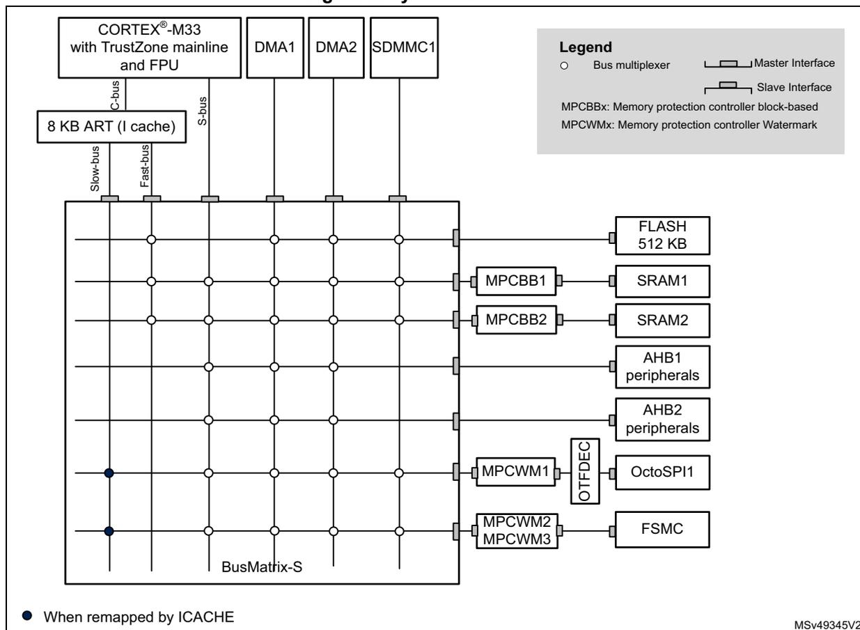
2.1.1 Fast C-bus
This bus connects the C-bus of the Cortex-M33 core to the BusMatrix via the instruction cache. This bus is used for instruction fetch and data access to the internal memories mapped in code region. The target of this bus are the internal flash and internal SRAMs.
2.1.2 Slow C-bus
This bus connects the C-bus of the Cortex-M33 core to the BusMatrix via the instruction cache. This bus is used for instruction fetch and data access to the external memories mapped in code region. The target of this bus are the external memories (FSMC and OCTOSPI).
2.1.3 S-bus
This bus connects the system bus of the Cortex-M33 core to the BusMatrix. This bus is used by the core to access data located in a peripheral or SRAM area. The targets of this bus are
the internal SRAMs, the AHB1 peripherals including the APB1 and APB2 peripherals, the AHB2 peripherals and the external memories through the OCTOSPI or the FSMC.
The SRAM2 is also accessible on this bus to allow continuous mapping with SRAM1.
2.1.4 DMA-bus
This bus connects the AHB master interface of the DMA to the BusMatrix. The targets of this bus are the SRAM1 and SRAM2, the AHB1 peripherals including the APB1 and APB2 peripherals, the AHB2 peripherals and the external memories through the OCTOSPI or the FSMC.
2.1.5 SDMMC controller DMA bus
This bus connects the SDMMC1 DMA master interface to the BusMatrix. This bus is used only by the SDMMC1 DMA to load/store data from/to memory. The targets of this bus are data memories: internal SRAMs (SRAM1, SRAM2), internal flash memory or external memories through FSMC or OCTOSPI.
2.1.6 BusMatrix
The BusMatrix manages the access arbitration between masters. The arbitration uses a Round Robin algorithm. The BusMatrix is composed of up to six masters (CPU AHB, system bus, Fast C-bus, Slow C-bus, DMA1, DMA2, SDMMC1) and up to seven slaves (FLASH, SRAM1, SRAM2, AHB1 (including APB1 and APB2), AHB2, OCTOSTPI1 and FSMC).
AHB/APB bridges
The two AHB/APB bridges provide full synchronous connections between the AHB and the two APB buses, allowing flexible selection of the peripheral frequency.
Refer to Section 2.3.2 for the address mapping of the peripherals connected to this bridge.
After each device reset, all peripheral clocks are disabled (except for the SRAM1/2 and flash memory interface). Before using a peripheral the user has to enable its clock in the RCC_AHBxENR and the RCC_APBxENR registers.
Note: When a 16- or 8-bit access is performed on an APB register, the access is transformed into a 32-bit access: the bridge duplicates the 16- or 8-bit data to feed the 32-bit vector.
2.2 TrustZone security architecture
The security architecture is based on Arm TrustZone with the Armv8-M main extension.
The TrustZone security is activated by the TZEN option bit in the FLASH_OPTR register.
When the TrustZone is enabled, the SAU (security attribution unit) and IDAU (implementation defined attribution unit) define the memory access permissions based on secure or non-secure state of the processor.
- • SAU: Up to eight SAU configurable regions are available for security attribution.
- • IDAU: It provides a first memory partition between non-secure and non-secure-callable regions. The IDAU memory map partition is not configurable and fixed by hardware implementation (refer to Figure 2 ). It is then combined with the results from the SAU security attribution and the most secure level between the two is selected.
Based on IDAU security attribution, the flash, system SRAMs and peripherals memory space is aliased twice for secure and non-secure state. However, the external memories space is not aliased.
The table below shows an example of typical eight SAU regions mapping based on IDAU regions. The user can split and choose the secure, non-secure or NSC regions for external memories as needed.
Table 1. Example of memory map security attribution versus SAU regions configuration (1)
| Region description | Address range | IDAU security attribution | SAU security attribution typical configuration | Final security attribution |
|---|---|---|---|---|
| Code - external memories | 0x0000_0000 0x07FF_FFFF | Non-secure | Secure, non-secure, or NSC | Secure, non-secure, or NSC |
| Code - flash memory and SRAM | 0x0800_0000 0x0BFF_FFFF | Non-secure | Non-secure | Non-secure |
| 0x0C00_0000 0x0FFF_FFFF | NSC | Secure or NSC | Secure or NSC | |
| Code - external memories | 0x1000_0000 0x17FF_FFFF | Non-secure | Non-secure | Non-secure |
| 0x1800_0000 0x1FFF_FFFF | Non-secure | Non-secure | Non-secure | |
| SRAM | 0x2000_0000 0x2FFF_FFFF | Non-secure | Non-secure | Non-secure |
| 0x3000_0000 0x3FFF_FFFF | NSC | Secure or NSC | Secure or NSC | |
| Peripherals | 0x4000_0000 0x4FFF_FFFF | Non-secure | Non-secure | Non-secure |
| 0x5000_0000 0x5FFF_FFFF | NSC | Secure or NSC | Secure or NSC | |
| External memories | 0x6000_0000 0xDFFF_FFFF | Non-secure | Secure, non-secure, or NSC | Secure, non-secure, or NSC |
1. Different colors highlights the different configurations: pink = non-secure, blue= NSC (non-secure callable), and green = secure, non-secure, or NSC.
2.2.1 Default TrustZone security state
When the TrustZone security is activated by the TZEN option bit in the FLASH_OPTR, the default system security state is:
- • CPU:
- – Cortex-M33 is in secure state after reset. The boot address must be in secure address (i.e. belonging to the secure part of the memory map).
- • Memory map:
- – SAU: is fully secure after reset. Consequently, the memory map is fully secure. Up to 8 SAU configurable regions are available for security attribution.
- • Flash:
- – Flash secure regions are defined by watermark user options.
- – Flash interface blocks (pages) are all non-Secure after reset (but the watermark configuration supersedes the block-based one in case of overlap).
- • SRAMs:
- – All SRAMs are secure after reset. MPCBB (memory protection block based controller) is configured as fully secure.
- • External memories:
- – FSMC, and OCTOSPI banks are secure after reset. MPCWM (memory protection watermark based controller) is secure.
- • All peripherals (except GPIOs) are non secure after reset. For TrustZone-aware peripherals, their secure configuration registers are secure.
Note: Refer to Table 2 and Table 3 for a list of securable and TrustZone-aware peripherals.
- • All GPIO are secure after reset.
- • Interrupts:
- – NVIC: All interrupts are secure after reset. NVIC is banked for secure and non-secure state.
- – TZIC: All illegal access interrupts are disabled after reset.
2.2.2 TrustZone peripheral classification
When the TrustZone security is active, a peripheral can be either securable or TrustZone-aware type as defined below:
- • securable: a peripheral is protected by an AHB/APB firewall gate that is controlled from TZSC controller to define security properties.
- • TrustZone-aware: a peripheral connected directly to AHB or APB bus and implementing a specific TrustZone behavior such as a subset of registers being secure. TrustZone-aware AHB masters always drive HNONSEC signal according to their security mode (as CM33 core and DMA).
Refer to Section 5.2.1: GTZC TrustZone system architecture
Table 2 and Table 3 summarize the list of Securables and TrustZone aware peripherals within the system.
Table 2. Securables peripherals by TZSC
| Bus | Peripheral |
|---|---|
| AHB3 | OCTOSPI1 registers |
| FMC registers | |
| AHB 2 | SDMMC1 |
| PKA | |
| RNG | |
| HASH | |
| AES | |
| ADC |
Table 2. Securable peripherals by TZSC (continued)
| Bus | Peripheral |
|---|---|
| AHB1 | ICACHE registers |
| TSC | |
| CRC | |
| APB2 | DFSDM1 |
| SAI2 | |
| SAI1 | |
| TIM17 | |
| TIM16 | |
| TIM15 | |
| USART1 | |
| TIM8 | |
| SPI1 | |
| TIM1 | |
| COMP | |
| VREFBUF | |
| APB1 | UCPD1 |
| USB FS | |
| FDCAN1 | |
| LPTIM3 | |
| LPTIM2 | |
| I2C4 | |
| LPUART1 | |
| LPTIM1 | |
| OPAMP | |
| DAC1/DAC2 | |
| CRS | |
| I2C3 | |
| I2C2 | |
| I2C1 | |
| UART5 | |
| UART4 | |
| USART3 | |
| USART2 | |
| SPI3 | |
| SPI2 |
Table 2. Securable peripherals by TZSC (continued)
| Bus | Peripheral |
|---|---|
| APB1 | IWDG |
| WWDG | |
| TIM7 | |
| TIM6 | |
| TIM5 | |
| TIM4 | |
| TIM3 | |
| TIM2 |
Table 3. TrustZone-aware peripherals
| Bus | Peripheral |
|---|---|
| AHB2 | GPIOH |
| GPIOG | |
| GPIOF | |
| GPIOE | |
| GPIO D | |
| GPIOC | |
| GPIOB | |
| GPIOA | |
| OTFDEC1 (1) | |
| AHB1 | GTZC |
| EXTI | |
| Flash memory | |
| RCC | |
| DMAMUX1 | |
| DMA2 | |
| DMA1 | |
| APB2 | SYSCFG |
| APB1 | PWR |
| RTC | |
| TAMP |
1. Always secure when TZEN = 1.
2.3 Memory organization
2.3.1 Introduction
Program memory, data memory, registers and I/O ports are organized within the same linear 4-Gbyte address space.
The bytes are coded in memory in Little Endian format. The lowest numbered byte in a word is considered the word's least significant byte and the highest numbered byte the most significant.
2.3.2 Memory map and register boundary addresses
Figure 2. Memory map based on IDAU mapping
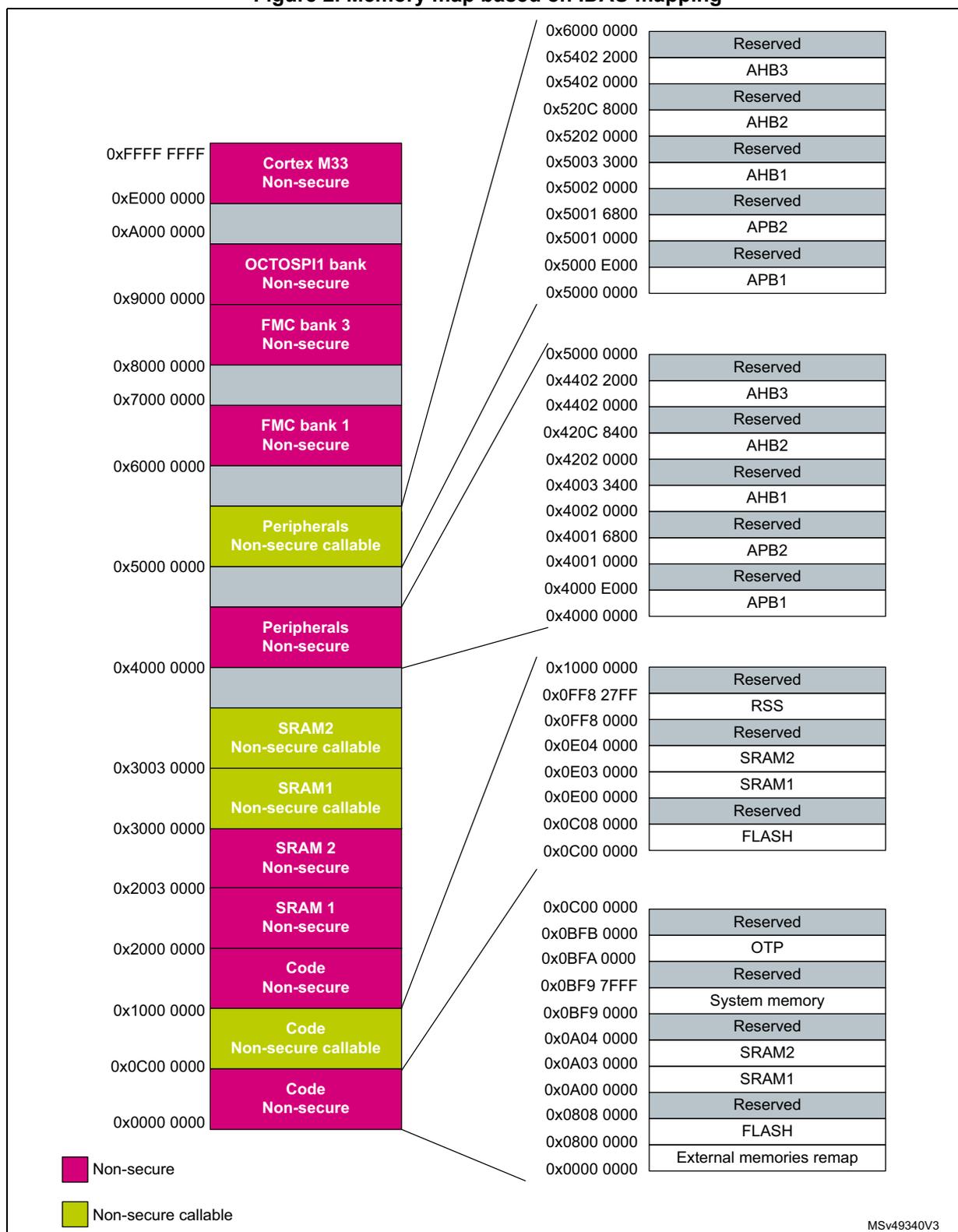
Memory Map Summary:
| Address Range | Memory Region | Security Attribute |
|---|---|---|
| 0x0000 0000 - 0x1000 0000 | Code | Non-secure |
| 0x1000 0000 - 0x2000 0000 | Code | Non-secure |
| 0x2000 0000 - 0x3000 0000 | SRAM 1 | Non-secure |
| 0x3000 0000 - 0x4000 0000 | SRAM 2 | Non-secure |
| 0x4000 0000 - 0x5000 0000 | SRAM1 | Non-secure callable |
| 0x5000 0000 - 0x6000 0000 | SRAM2 | Non-secure callable |
| 0x6000 0000 - 0x7000 0000 | Peripherals | Non-secure |
| 0x7000 0000 - 0x8000 0000 | Peripherals | Non-secure callable |
| 0x8000 0000 - 0x9000 0000 | FMC bank 1 | Non-secure |
| 0x9000 0000 - 0xA000 0000 | FMC bank 3 | Non-secure |
| 0xA000 0000 - 0xE000 0000 | OCTOSPI1 bank | Non-secure |
| 0xE000 0000 - 0xFFFF FFFF | Cortex M33 | Non-secure |
Register Boundary Addresses:
- 0x0000 0000 - 0x1000 0000:
- 0x0000 0000: External memories remap
- 0x0800 0000: FLASH
- 0x0808 0000: Reserved
- 0xA000 0000: SRAM1
- 0xA03 0000: SRAM2
- 0x0BF9 0000: Reserved
- 0x0BF9 7FFF: System memory
- 0x0BFA 0000: Reserved
- 0x0BFB 0000: OTP
- 0x0C00 0000: Reserved
- 0x1000 0000 - 0x2000 0000:
- 0x1000 0000: Reserved
- 0x0FF8 27FF: RSS
- 0x0FF8 0000: Reserved
- 0x0E04 0000: SRAM2
- 0x0E03 0000: SRAM1
- 0x0E00 0000: Reserved
- 0x0C08 0000: FLASH
- 0x0C00 0000: Reserved
- 0x4000 0000 - 0x5000 0000:
- 0x4000 0000: APB1
- 0x4000 E000: Reserved
- 0x4001 0000: APB2
- 0x4001 6800: Reserved
- 0x4002 0000: AHB1
- 0x4003 3400: Reserved
- 0x4202 0000: AHB2
- 0x420C 8400: Reserved
- 0x4402 0000: AHB3
- 0x4402 2000: Reserved
- 0x5000 0000 - 0x6000 0000:
- 0x5000 0000: APB1
- 0x5000 E000: Reserved
- 0x5001 0000: APB2
- 0x5001 6800: Reserved
- 0x5002 0000: AHB1
- 0x5202 0000: AHB2
- 0x520C 8000: Reserved
- 0x5402 0000: AHB3
- 0x5402 2000: Reserved
Legend:
- Non-secure (Pink)
- Non-secure callable (Green)
MSv49340V3
All the memory map areas that are not allocated to memories and peripherals are considered “Reserved”. For the detailed mapping of available memory and register areas, refer to the following table.
The following table gives the boundary addresses of the peripherals available in the devices.
Table 4. STM32L552xx and STM32L562xx memory map and peripheral register boundary addresses
| Bus | Secure boundary address | Non-secure boundary address | Size (bytes) | Peripheral | Peripheral register map |
|---|---|---|---|---|---|
| AHB3 | 0x5402 1400 - 0x5FFF FFFF | 0x4402 1400 - 0x4FFF FFFF | 129 MB | Reserved | - |
| 0x5402 1000 - 0x5402 13FF | 0x4402 1000 - 0x4402 13FF | 1 KB | OCTOSPI1 registers | Section 20.7.28: OCTOSPI register map | |
| 0x5402 0400 - 0x5402 0FFF | 0x4402 0400 - 0x4402 0FFF | 3 KB | Reserved | - | |
| 0x5402 0000 - 0x5402 03FF | 0x4402 0000 - 0x4402 03FF | 1 KB | FMC registers | Section 19.7.8: FMC register map | |
| AHB2 | 0x520C 8400 - 0x5401 FFFF | 0x420C 8400 - 0x4401 FFFF | 32 MB | Reserved | - |
| 0x520C 8000 - 0x520C 83FF | 0x420C 8000 - 0x420C 83FF | 1 KB | SDMMC1 | Section 48.9.20: SDMMC register map | |
| 0x520C 5400 - 0x520C 7FFF | 0x420C 5400 - 0x420C 7FFF | 11 KB | Reserved | - | |
| 0x520C 5000 - 0x520C 53FF | 0x420C 5000 - 0x420C 53FF | 1 KB | OTFDEC1 | Section 31.6.15: OTFDEC register map | |
| 0x520C 4000 - 0x520C 4FFF | 0x420C 4000 - 0x420C 4FFF | 4 KB | Reserved | - | |
| 0x520C 2000 - 0x520C 3FFF | 0x420C 2000 - 0x420C 3FFF | 8 KB | PKA | Section 32.7.5: PKA register map | |
| 0x520C 0C00 - 0x520C 1FFF | 0x420C 0C00 - 0x420C 1FFF | 5 KB | Reserved | - | |
| 0x520C 0800 - 0x520C 0BFF | 0x420C 0800 - 0x420C 0BFF | 1 KB | RNG | Section 28.7.5: RNG register map | |
| 0x520C 0400 - 0x520C 07FF | 0x420C 0400 - 0x420C 07FF | 1 KB | HASH | Section 30.6.8: HASH register map | |
| 0x520C 0000 - 0x520C 03FF | 0x420C 0000 - 0x420C 03FF | 1 KB | AES | Section 29.7.18: AES register map | |
| 0x5202 8400 - 0x520B FFFF | 0x4202 8400 - 0x420B FFFF | 609 KB | Reserved | - | |
| 0x5202 8000 - 0x5202 83FF | 0x4202 8000 - 0x4202 83FF | 1 KB | ADC | Section 21.9: ADC register map on page 792 | |
| 0x5202 2000 - 0x5202 7FFF | 0x4202 2000 - 0x4202 7FFF | 24 KB | Reserved | - | |
| 0x5202 1C00 - 0x5202 1FFF | 0x4202 1C00 - 0x4202 1FFF | 1 KB | GPIOH | Section 11.6.13: GPIO register map | |
| 0x5202 1800 - 0x5202 1BFF | 0x4202 1800 - 0x4202 1BFF | 1 KB | GPIOG | Section 11.6.13: GPIO register map | |
| 0x5202 1400 - 0x5202 17FF | 0x4202 1400 - 0x4202 17FF | 1 KB | GPIOF | Section 11.6.13: GPIO register map |
Table 4. STM32L552xx and STM32L562xx memory map and peripheral register boundary addresses (continued)
| Bus | Secure boundary address | Non-secure boundary address | Size (bytes) | Peripheral | Peripheral register map |
|---|---|---|---|---|---|
| AHB2 (continued) | 0x5202 1000 - 0x5202 13FF | 0x4202 1000 - 0x4202 13FF | 1 KB | GPIOE | Section 11.6.13: GPIO register map |
| 0x5202 0C00 - 0x5202 0FFF | 0x4202 0C00 - 0x4202 0FFF | 1 KB | GPIOE | Section 11.6.13: GPIO register map | |
| 0x5202 0800 - 0x5202 0BFF | 0x4202 0800 - 0x4202 0BFF | 1 KB | GPIOC | Section 11.6.13: GPIO register map | |
| 0x5202 0400 - 0x5202 07FF | 0x4202 0400 - 0x4202 07FF | 1 KB | GPIOB | Section 11.6.13: GPIO register map | |
| 0x5202 0000 - 0x5202 03FF | 0x4202 0000 - 0x4202 03FF | 1 KB | GPIOA | Section 11.6.13: GPIO register map | |
| AHB1 | 0x5003 4000 - 0x5201 FFFF | 0x4003 3400 - 0x4201 FFFF | 32 MB | Reserved | - |
| 0x5003 2400 - 0x5003 33FF | 0x4003 2400 - 0x4003 33FF | 4 KB | GTZC | Section 5.6.5: GTZC_MPCBB1 register map and reset values Section 5.6.6: GTZC_MPCBB2 register map and reset values Section 5.7.10: GTZC_TZIC register map and reset values Section 5.5.8: GTZC_TZSC register map and reset values | |
| 0x5003 0800 - 0x5003 23FF | 0x4003 0800 - 0x4003 23FF | 7 KB | Reserved | - | |
| 0x5003 0400 - 0x5003 07FF | 0x4003 0400 - 0x4003 07FF | 1 KB | ICache | Section 7.7.8: ICACHE register map | |
| 0x5002 F800 - 0x5003 03FF | 0x4002 F800 - 0x4003 03FF | 3 KB | Reserved | - | |
| 0x5002 F400 - 0x5002 F7FF | 0x4002 F400 - 0x4002 F7FF | 1 KB | EXTI | Section 17.6.21: EXTI register map | |
| 0x5002 4400 - 0x5002 F3FF | 0x4002 4400 - 0x4002 F3FF | 43 KB | Reserved | - | |
| 0x5002 4000 - 0x5002 43FF | 0x4002 4000 - 0x4002 43FF | 1 KB | TSC | Section 27.6.11: TSC register map | |
| 0x5002 3400 - 0x5002 3FFF | 0x4002 3400 - 0x4002 3FFF | 3 KB | Reserved | - | |
| 0x5002 3000 - 0x5002 33FF | 0x4002 3000 - 0x4002 33FF | 1 KB | CRC | Section 18.4.6: CRC register map | |
| 0x5002 2400 - 0x5002 2FFF | 0x4002 2400 - 0x4002 2FFF | 3 KB | Reserved | - | |
| 0x5002 2000 - 0x5002 23FF | 0x4002 2000 - 0x4002 23FF | 1 KB | Flash registers | Section 6.9.28: FLASH register map and reset values |
Table 4. STM32L552xx and STM32L562xx memory map and peripheral register boundary addresses (continued)
| Bus | Secure boundary address | Non-secure boundary address | Size (bytes) | Peripheral | Peripheral register map |
|---|---|---|---|---|---|
| AHB1 (continued) | 0x5002 1400 - 0x5002 1FFF | 0x4002 1400 - 0x4002 1FFF | 3 KB | Reserved | - |
| 0x5002 1000 - 0x5002 13FF | 0x4002 1000 - 0x4002 13FF | 1 KB | RCC | Section 9.8.42: RCC register map | |
| 0x5002 0C00 - 0x5002 0FFF | 0x4002 0C00 - 0x4002 0FFF | 1 KB | Reserved | - | |
| 0x5002 0800 - 0x5002 0BFF | 0x4002 0800 - 0x4002 0BFF | 1 KB | DMAMUX1 | Section 15.6.7: DMAMUX register map | |
| 0x5002 0400 - 0x5002 07FF | 0x4002 0400 - 0x4002 07FF | 1 KB | DMA2 | Section 14.6.8: DMA register map | |
| 0x5002 0000 - 0x5002 03FF | 0x4002 0000 - 0x4002 03FF | 1 KB | DMA1 | Section 14.6.8: DMA register map | |
| APB2 | 0x5001 6800 - 0x5001 FFFF | 0x4001 6800 - 0x4001 FFFF | 38 KB | Reserved | - |
| 0x5001 6000 - 0x5001 67FF | 0x4001 6000 - 0x4001 67FF | 2 KB | DFSDM1 | Section 26.8.16: DFSDM register map | |
| 0x5001 5C00 - 0x5001 5FFF | 0x4001 5C00 - 0x4001 5FFF | 1 KB | Reserved | - | |
| 0x5001 5800 - 0x5001 5BFF | 0x4001 5800 - 0x4001 5BFF | 1 KB | SAI2 | Section 47.6.20: SAI register map | |
| 0x5001 5400 - 0x5001 57FF | 0x4001 5400 - 0x4001 57FF | 1 KB | SAI1 | Section 47.6.20: SAI register map | |
| 0x5001 4C00 - 0x5001 53FF | 0x4001 4C00 - 0x4001 53FF | 2 KB | Reserved | - | |
| 0x5001 4800 - 0x5001 4BFF | 0x4001 4800 - 0x4001 4BFF | 1 KB | TIM17 | Section 35.6.21: TIM16/TIM17 register map | |
| 0x5001 4400 - 0x5001 47FF | 0x4001 4400 - 0x4001 47FF | 1 KB | TIM16 | Section 35.6.21: TIM16/TIM17 register map | |
| 0x5001 4000 - 0x5001 43FF | 0x4001 4000 - 0x4001 43FF | 1 KB | TIM15 | Section 35.5.21: TIM15 register map | |
| 0x5001 3C00 - 0x5001 3FFF | 0x4001 3C00 - 0x4001 3FFF | 1 KB | Reserved | - | |
| 0x5001 3800 - 0x5001 3BFF | 0x4001 3800 - 0x4001 3BFF | 1 KB | USART1 | Section 44.8.15: USART register map | |
| 0x5001 3400 - 0x5001 37FF | 0x4001 3400 - 0x4001 37FF | 1 KB | TIM8 | Section 33.4.33: TIM8 register map | |
| 0x5001 3000 - 0x5001 33FF | 0x4001 3000 - 0x4001 33FF | 1 KB | SPI1 | Section 46.6.8: SPI register map | |
| 0x5001 2C00 - 0x5001 2FFF | 0x4001 2C00 - 0x4001 2FFF | 1 KB | TIM1 | Section 33.4.32: TIM1 register map |
Table 4. STM32L552xx and STM32L562xx memory map and peripheral register boundary addresses (continued)
| Bus | Secure boundary address | Non-secure boundary address | Size (bytes) | Peripheral | Peripheral register map |
|---|---|---|---|---|---|
| APB2 (continued) | 0x5001 0400 - 0x5001 2BFF | 0x4001 0400 - 0x4001 2BFF | 10 KB | Reserved | - |
| 0x5001 0200 - 0x5001 03FF | 0x4001 0200 - 0x4001 03FF | 1 KB | COMP | Section 24.6.3: COMP register map | |
| 0x5001 0100 - 0x5001 01FF | 0x4001 0100 - 0x4001 01FF | 1 KB | VREFBUF | Section 23.4.3: VREFBUF register map | |
| 0x5001 0000 - 0x5001 002F | 0x4001 0000 - 0x4001 002F | 1 KB | SYSCFG | Section 12.3.12: SYSCFG register map | |
| APB1 | 0x5000 E000 - 0x5000 FFFF | 0x4000 E000 - 0x4000 FFFF | 8 KB | Reserved | - |
| 0x5000 DC00 - 0x5000 DFFF | 0x4000 DC00 - 0x4000 DFFF | 1 KB | UCPD1 | Section 51.8.15: UCPD register map | |
| 0x5000 D800 - 0x5000 DBFF | 0x4000 D800 - 0x4000 DBFF | 1 KB | USB SRAM | Section 50.6.3: USB register map | |
| 0x5000 D400 - 0x5000 D7FF | 0x4000 D400 - 0x4000 D7FF | 1 KB | USB FS | Section 50.6.3: USB register map | |
| 0x5000 B000 - 0x5000 D3FF | 0x4000 B000 - 0x4000 D3FF | 9 KB | Reserved | - | |
| 0x5000 AC00 - 0x5000 AFFF | 0x4000 AC00 - 0x4000 AFFF | 1 KB | FDCAN RAM | Section 49.4.38: FDCAN register map | |
| 0x5000 A800 - 0x5000 ABFF | 0x4000 A800 - 0x4000 ABFF | 1 KB | Reserved | - | |
| 0x5000 A400 - 0x5000 A7FF | 0x4000 A400 - 0x4000 A7FF | 1 KB | FDCAN1 | Section 49.4.38: FDCAN register map | |
| 0x5000 9C00 - 0x5000 A3FF | 0x4000 9C00 - 0x4000 A3FF | 2 KB | Reserved | - | |
| 0x5000 9800 - 0x5000 9BFF | 0x4000 9800 - 0x4000 9BFF | 1 KB | LPTIM3 | Section 37.7.13: LPTIM register map | |
| 0x5000 9400 - 0x5000 97FF | 0x4000 9400 - 0x4000 97FF | 1 KB | LPTIM2 | Section 37.7.13: LPTIM register map | |
| 0x5000 8800 - 0x5000 93FF | 0x4000 8800 - 0x4000 93FF | 3 KB | Reserved | - | |
| 0x5000 8400 - 0x5000 87FF | 0x4000 8400 - 0x4000 87FF | 1 KB | I2C4 | Section 43.9.12: I2C register map | |
| 0x5000 8000 - 0x5000 83FF | 0x4000 8000 - 0x4000 83FF | 1 KB | LPUART1 | - | |
| 0x5000 7C00 - 0x5000 7FFF | 0x4000 7C00 - 0x4000 7FFF | 1 KB | LPTIM1 | Section 37.7.13: LPTIM register map | |
| 0x5000 7800 - 0x5000 7BFF | 0x4000 7800 - 0x4000 7BFF | 1 KB | OPAMP | Section 25.5: OPAMP registers |
Table 4. STM32L552xx and STM32L562xx memory map and peripheral register boundary addresses (continued)
| Bus | Secure boundary address | Non-secure boundary address | Size (bytes) | Peripheral | Peripheral register map |
|---|---|---|---|---|---|
| APB1 (continued) | 0x5000 7400 - 0x5000 77FF | 0x4000 7400 - 0x4000 77FF | 1 KB | DAC | Section 22.7.21: DAC register map |
| 0x5000 7000 - 0x5000 73FF | 0x4000 7000 - 0x4000 73FF | 1 KB | PWR | Section 8.6.26: PWR register map and reset values | |
| 0x5000 6400 - 0x5000 6FFF | 0x4000 6400 - 0x4000 6FFF | 3 KB | Reserved | - | |
| 0x5000 6000 - 0x5000 63FF | 0x4000 6000 - 0x4000 63FF | 1 KB | CRS | Section 10.7.5: CRS register map | |
| 0x5000 5C00 - 0x5000 5FFF | 0x4000 5C00 - 0x4000 5FFF | 1 KB | I2C3 | Section 43.9.12: I2C register map | |
| 0x5000 5800 - 0x5000 5BFF | 0x4000 5800 - 0x4000 5BFF | 1 KB | I2C2 | Section 43.9.12: I2C register map | |
| 0x5000 5400 - 0x5000 57FF | 0x4000 5400 - 0x4000 57FF | 1 KB | I2C1 | Section 43.9.12: I2C register map | |
| 0x5000 5000 - 0x5000 53FF | 0x4000 5000 - 0x4000 53FF | 1 KB | UART5 | Section 44.8.15: USART register map | |
| 0x5000 4C00 - 0x5000 4FFF | 0x4000 4C00 - 0x4000 4FFF | 1 KB | UART4 | Section 44.8.15: USART register map | |
| 0x5000 4800 - 0x5000 4BFF | 0x4000 4800 - 0x4000 4BFF | 1 KB | USART3 | Section 44.8.15: USART register map | |
| 0x5000 4400 - 0x5000 47FF | 0x4000 4400 - 0x4000 47FF | 1 KB | USART2 | Section 44.8.15: USART register map | |
| 0x5000 4000 - 0x5000 43FF | 0x4000 4000 - 0x4000 43FF | 1 KB | Reserved | - | |
| 0x5000 3C00 - 0x5000 3FFF | 0x4000 3C00 - 0x4000 3FFF | 1 KB | SPI3 | Section 46.6.8: SPI register map | |
| 0x5000 3800 - 0x5000 3BFF | 0x4000 3800 - 0x4000 3BFF | 1 KB | SPI2 | Section 46.6.8: SPI register map | |
| 0x5000 3400 - 0x5000 37FF | 0x4000 3400 - 0x4000 37FF | 1 KB | TAMP | Section 42.6.19: TAMP register map | |
| 0x5000 3000 - 0x5000 33FF | 0x4000 3000 - 0x4000 33FF | 1 KB | IWDG | Section 39.4.6: IWDG register map | |
| 0x5000 2C00 - 0x5000 2FFF | 0x4000 2C00 - 0x4000 2FFF | 1 KB | WWDG | Section 40.5.4: WWDG register map | |
| 0x5000 2800 - 0x5000 2BFF | 0x4000 2800 - 0x4000 2BFF | 1 KB | RTC | Section 41.6.24: RTC register map | |
| 0x5000 1800 - 0x5000 27FF | 0x4000 1800 - 0x4000 27FF | 4 KB | Reserved | - | |
| 0x5000 1400 - 0x5000 17FF | 0x4000 1400 - 0x4000 17FF | 1 KB | TIM7 | Section 36.4.9: TIMx register map |
| Bus | Secure boundary address | Non-secure boundary address | Size (bytes) | Peripheral | Peripheral register map |
|---|---|---|---|---|---|
| APB1 (continued) | 0x5000 1000 - 0x5000 13FF | 0x4000 1000 - 0x4000 13FF | 1 KB | TIM6 | Section 36.4.9: TIMx register map |
| 0x5000 0C00 - 0x5000 0FFF | 0x4000 0C00 - 0x4000 0FFF | 1 KB | TIM5 | Section 34.4.26: TIMx register map | |
| 0x5000 0800 - 0x5000 0BFF | 0x4000 0800 - 0x4000 0BFF | 1 KB | TIM4 | Section 34.4.26: TIMx register map | |
| 0x5000 0400 - 0x5000 07FF | 0x4000 0400 - 0x4000 07FF | 1 KB | TIM3 | Section 34.4.26: TIMx register map | |
| 0x5000 0000 - 0x5000 03FF | 0x4000 0000 - 0x4000 03FF | 1 KB | TIM2 | Section 34.4.26: TIMx register map |
2.4 Embedded SRAM
The STM32L552xx and STM32L562xx devices feature up to 256 Kbytes SRAM:
- • 192 Kbytes SRAM1
- • 64 Kbytes SRAM2
These SRAM can be accessed as bytes, half-words (16 bits) or full words (32 bits). These memories can be addressed at maximum system clock frequency without wait state and thus by both CPU and DMA.
The CPU can access the SRAM1 and SRAM2 through the system bus or through the C-bus depending on the selected address.
Either 64 Kbytes or upper 4 Kbytes of SRAM2 can be retained in Standby mode.
When the TrustZone security is enabled, all SRAMs are secure after reset. The SRAM can be programmed as non-secure with a block granularity, using MPCBB (memory protection controller block configuration based) in GTZC controller. The granularity of SRAM secure/non-secure block-based is a page of 256 bytes.
2.4.1 SRAM2 parity check
The user can enable the SRAM2 parity check using the option bit SRAM2_PE in the OPTTR user option register (refer to Section 6.4.1: Option bytes description ).
The data bus width is 36 bits because 4 bits are available for parity check (1 bit per byte) in order to increase memory robustness, as required for instance by Class B or SIL safety standards.
The parity bits are computed and stored when writing into the SRAM2. Then, they are automatically checked when reading. If one bit fails, an NMI is generated. The same error can also be linked to the BRK_IN Break input of TIM1/TIM8/TIM15/TIM16/TIM17 with the SPL control bit in the SYSCFG configuration register 2 (SYSCFG_CFGR2) . The SRAM2 Parity Error flag (SPF) is available in the SYSCFG configuration register 2 (SYSCFG_CFGR2) .
Note: When enabling the RAM parity check, it is advised to initialize by software the whole RAM memory at the beginning of the code, to avoid getting parity errors when reading non-initialized locations.
2.4.2 SRAM2 Write protection
The SRAM2 can be write protected with a page granularity of 1 Kbyte.
Table 5. SRAM2 organization
| Page number | Start address | End address |
|---|---|---|
| Page 0 | 0x2003 0000 | 0x2003 03FF |
| Page 1 | 0x2003 0400 | 0x2003 07FF |
| Page 2 | 0x2003 0800 | 0x2003 0BFF |
| Page 3 | 0x2003 0C00 | 0x2003 0FFF |
| Page 4 | 0x2003 1000 | 0x2003 13FF |
| Page 5 | 0x2003 1400 | 0x2003 17FF |
| Page 6 | 0x2003 1800 | 0x2003 1BFF |
| Page 7 | 0x2003 1C00 | 0x2003 1FFF |
| Page 8 | 0x2003 2000 | 0x2003 23FF |
| Page 9 | 0x2003 2400 | 0x2003 27FF |
| Page 10 | 0x2003 2800 | 0x2003 2BFF |
| Page 11 | 0x2003 2C00 | 0x2003 2FFF |
| Page 12 | 0x2003 3000 | 0x2003 33FF |
| Page 13 | 0x2003 3400 | 0x2003 37FF |
| Page 14 | 0x2003 3800 | 0x2003 3BFF |
| Page 15 | 0x2003 3C00 | 0x2003 3FFF |
| Page 16 | 0x2003 4000 | 0x2003 43FF |
| Page 17 | 0x2003 4400 | 0x2003 47FF |
| Page 18 | 0x2003 4800 | 0x2003 4BFF |
| Page 19 | 0x2003 4C00 | 0x2003 4FFF |
| Page 20 | 0x2003 5000 | 0x2003 53FF |
| Page 21 | 0x2003 5400 | 0x2003 57FF |
| Page 22 | 0x2003 5800 | 0x2003 5BFF |
| Page 23 | 0x2003 5C00 | 0x2003 5FFF |
| Page 24 | 0x2003 6000 | 0x2003 63FF |
| Page 25 | 0x2003 6400 | 0x2003 67FF |
| Page 26 | 0x2003 6800 | 0x2003 6BFF |
| Page 27 | 0x2003 6C00 | 0x2003 6FFF |
| Page 28 | 0x2003 7000 | 0x2003 73FF |
Table 5. SRAM2 organization (continued)
| Page number | Start address | End address |
|---|---|---|
| Page 29 | 0x2003 7400 | 0x2003 77FF |
| Page 30 | 0x2003 7800 | 0x2003 7BFF |
| Page 31 | 0x2003 7C00 | 0x2003 7FFF |
| Page 32 | 0x2003 8000 | 0x2003 83FF |
| Page 33 | 0x2003 8400 | 0x2003 87FF |
| Page 34 | 0x2003 8800 | 0x2003 8BFF |
| Page 35 | 0x2003 8C00 | 0x2003 8FFF |
| Page 36 | 0x2003 9000 | 0x2003 93FF |
| Page 37 | 0x2003 9400 | 0x2003 97FF |
| Page 38 | 0x2003 9800 | 0x2003 9BFF |
| Page 39 | 0x2003 9C00 | 0x2003 9FFF |
| Page 40 | 0x2003 A000 | 0x2003 A3FF |
| Page 41 | 0x2003 A400 | 0x2003 A7FF |
| Page 42 | 0x2003 A800 | 0x2003 ABFF |
| Page 43 | 0x2003 AC00 | 0x2003 AFFF |
| Page 44 | 0x2003 B000 | 0x2003 B3FF |
| Page 45 | 0x2003 B400 | 0x2003 B7FF |
| Page 46 | 0x2003 B800 | 0x2003 BBFF |
| Page 47 | 0x2003 BC00 | 0x2003 BFFF |
| Page 48 | 0x2003 C000 | 0x2003 C3FF |
| Page 49 | 0x2003 C400 | 0x2003 C7FF |
| Page 50 | 0x2003 C800 | 0x2003 CBFF |
| Page 51 | 0x2003 CC00 | 0x2003 CFFF |
| Page 52 | 0x2003 D000 | 0x2003 D3FF |
| Page 53 | 0x2003 D400 | 0x2003 D7FF |
| Page 54 | 0x2003 D800 | 0x2003 DBFF |
| Page 55 | 0x2003 DC00 | 0x2003 DFFF |
| Page 56 | 0x2003 E000 | 0x2003 E3FF |
| Page 57 | 0x2003 E400 | 0x2003 E7FF |
| Page 58 | 0x2003 E800 | 0x2003 EBFF |
| Page 59 | 0x2003 EC00 | 0x2003 EFFF |
| Page 60 | 0x2003 F000 | 0x2003 F3FF |
| Page 61 | 0x2003 F400 | 0x2003 F7FF |
| Page 62 | 0x2003 F800 | 0x2003 FBFF |
| Page 63 | 0x2003 FC00 | 0x2003 FFFF |
The write protection can be enabled in SYSCFG SRAM2 write protection register (SYSCFG_SWPR) in the SYSCFG block. This is a register with write '1' once mechanism, which means that writing '1' on a bit will setup the write protection for that page of SRAM and it can be removed/cleared by a system reset only.
2.4.3 SRAM2 Read protection
The SRAM2 is protected with the Read protection (RDP). Refer to Section 6.7.2: Readout protection (RDP) for more details.
2.4.4 SRAM2 Erase
The SRAM2 can be erased with a system reset using the option bit SRAM2_RST in the OPTR user option register (refer to Section 6.4.1: Option bytes description ).
The SRAM2 erase can also be requested by software by setting the bit SRAM2ER in the SYSCFG SRAM2 control and status register (SYSCFG_SCSR) .
The SRAM2 is also erased by a Backup domain reset.
2.5 Flash memory overview
The flash memory is composed of two distinct physical areas:
- • The main flash memory block. It contains the application program and user data if necessary.
- • The information block. It is composed of three parts:
- – Option bytes for hardware and memory protection user configuration.
- – System memory that contains the ST proprietary code.
- – OTP (one-time programmable) area
The flash interface implements instruction access and data access based on the AHB protocol. It also implements the logic necessary to carry out the flash memory operations (program/erase) controlled through the flash registers plus security access control features. Refer to Section 6: Embedded flash memory (FLASH) for more details.
3 Boot configuration
At startup, a BOOT0 pin, nBOOT0 and NSBOOTADDx[24:0] / SECBOOTADD0[24:0] option bytes are used to select the boot memory address which includes:
- • Boot from any address in user flash
- • Boot from system memory bootloader
- • Boot from any address in embedded SRAM
- • Boot from Root Security service (RSS)
The BOOT0 value may come from the PH3-BOOT0 pin or from an option bit depending on the value of a user option bit to free the GPIO pad if needed.
Refer to Table 6 and Table 7 for boot modes when TrustZone is disabled and enabled respectively.
Table 6. Boot modes when TrustZone is disabled (TZEN=0)
| nBOOT0 FLASH_ OPTR[27] | BOOT0 pin PH3 | nSWBOOT0 FLASH_ OPTR[26] | Boot address option- bytes selection | Boot area | ST programmed default value |
|---|---|---|---|---|---|
| - | 0 | 1 | NSBOOTADD0[24:0] | Boot address defined by user option bytes NSBOOTADD0[24:0] | Flash: 0x0800 0000 |
| - | 1 | 1 | NSBOOTADD1[24:0] | Boot address defined by user option bytes NSBOOTADD1[24:0] | System bootloader: 0x0BF9 0000 |
| 1 | - | 0 | NSBOOTADD0[24:0] | Boot address defined by user option bytes NSBOOTADD0[24:0] | Flash: 0x0800 0000 |
| 0 | - | 0 | NSBOOTADD1[24:0] | Boot address defined by user option bytes NSBOOTADD1[24:0] | System bootloader: 0x0BF9 0000 |
When TrustZone is enabled by setting the TZEN option bit, the boot space must be in secure area. The SECBOOTADD0[24:0] option bytes are used to select the boot secure memory address.
A unique boot entry option can be selected by setting the BOOT_LOCK option bit. All other boot options are ignored.
Table 7. Boot modes when TrustZone is enabled (TZEN=1)
| BOOT_LOCK | nBOOT0 FLASH_OPTR[27] | BOOT0 pin PH3 | nSWBOOT0 FLASH_OPTR[26] | RSS command | Boot address option-bytes selection | Boot area | ST programmed default value |
|---|---|---|---|---|---|---|---|
| 0 | - | 0 | 1 | 0 | SECBOOTADD0 [24:0] | Secure boot address defined by user option bytes SECBOOTADD0 [24:0] | Flash: 0x0C00 0000 |
| - | 1 | 1 | 0 | N/A | RSS: 0x0FF8 0000 | RSS: 0x0FF8 0000 | |
| 1 | - | 0 | 0 | SECBOOTADD0 [24:0] | Secure boot address defined by user option bytes SECBOOTADD0 [24:0] | Flash: 0x0C00 0000 | |
| 0 | - | 0 | 0 | N/A | RSS: RSS: 0x0FF8 0000 | RSS: 0x0FF8 0000 | |
| - | - | - | ≠ 0 | N/A | RSS: RSS: 0x0FF8 0000 | RSS: 0x0FF8 0000 | |
| 1 | - | - | - | - | SECBOOTADD0 [24:0] | Secure boot address defined by user option bytes SECBOOTADD0 [24:0] | Flash: 0x0C00 0000 |
The boot address option bytes enables the possibility to program any boot memory address. However, the allowed address space depends on flash read protection RDP level.
If the programmed boot memory address is out of the allowed memory mapped area when RDP level is 0.5 or more, the default boot fetch address is forced to:
- • 0x0800 0000 (when TZEN = 0)
- • RSS (when TZEN = 1)
Refer to the Table 8 .
Table 8. Boot space versus RDP protection
| RDP | TZEN = 1 | TZEN = 0 |
|---|---|---|
| 0 | Any boot address | Any boot address |
| 0.5 | N/A | |
| 1 | Boot address only in: RSS: 0x0FF80000 or secure flash: 0x0C000000 - 0x0C07 FFFF | Any boot address |
| 2 | Otherwise the boot address is forced to RSS | Boot address only in flash 0x0800 0000 - 0x0807 FFFF Otherwise the forced boot address is: 0x0800 0000 (1) |
- 1. In RDP level 2, the boot is done from the address programmed in NSBOOTADD0 or NSBOOTADD1 depending on the boot configuration before setting the RDP level 2 and if the programmed address is within the user flash memory.
If the programmed NSBOOTADD0 or NSBOOTADD1 is not a valid address, the boot is forced at 0x800 0000.
The BOOT0 value (either coming from the pin or the option bit) is latched upon reset release. It is up to the user to set nBOOT0 or BOOT0 values to select the required boot mode.
The BOOT0 pin or user option bit (depending on the nSWBOOT0 bit value in the FLASH_OPTR register) is also re-sampled when exiting from Standby mode. Consequently, they must be kept in the required Boot mode configuration in Standby mode. After startup delay, the selection of the boot area is done before releasing the processor reset.
PH3/BOOT0 GPIO is configured in:
- • Input mode during the complete reset phase if the option bit nSWBOOT0 is set into the FLASH_OPTR register and then switches automatically in analog mode after reset is released (BOOT0 pin).
- • Input mode from the reset phase to the completion of the option byte loading if the bit nSWBOOT0 is cleared into the FLASH_OPTR register (BOOT0 value coming from the option bit). It switches then automatically to the analog mode even if the reset phase is not complete.
Embedded bootloader and RSS
The bootloader is located in the system memory. It is used to reprogram the flash memory by using USART, I2C, SPI, FDCAN or USB FS in device mode through the DFU (device firmware upgrade). It is programmed by ST during production. Refer to AN2606, STM32 microcontroller system memory boot mode .
The root secure services (RSS) are embedded in a flash memory area named secure information block, programmed during ST production.
The RSS enables for example the secure firmware installation (SFI) thanks to the RSS extension firmware (RSSe SFI).
This feature allows the customers to protect the confidentiality of the firmware to be provisioned into the STM32 device when the production is subcontracted to a third party.
The RSS is available on all devices, after enabling the TrustZone through the TZEN option bit.