18. Quad-SPI interface (QUADSPI)
18.1 Introduction
The QUADSPI is a specialized communication interface targeting single, dual- or quad-SPI flash memories. It can operate in any of the three following modes:
- • indirect mode: all the operations are performed using the QUADSPI registers.
- • automatic status-polling mode: the external flash memory status register is periodically read and an interrupt can be generated in case of flag setting.
- • memory-mapped mode: the external flash memory is mapped to the device address space and is seen by the system as if it was an internal memory.
18.2 QUADSPI main features
- • Three functional modes: indirect, automatic status-polling, and memory-mapped
- • SDR and DDR support
- • Fully programmable opcode for both indirect and memory-mapped modes
- • Fully programmable frame format for both indirect and memory-mapped modes
- • Integrated FIFO for reception and transmission
- • 8-, 16-, and 32-bit data accesses allowed
- • DMA channel for indirect mode operations
- • Interrupt generation on FIFO threshold, timeout, operation complete, and access error
18.3 QUADSPI functional description
18.3.1 QUADSPI block diagram
Figure 45. QUADSPI block diagram
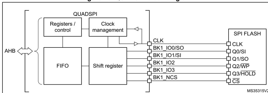
The diagram illustrates the internal architecture of the QUADSPI interface. On the left, an AHB bus connects to a 'Registers / control' block and a 'FIFO' block. The 'Registers / control' block is also connected to a 'Clock management' block. The 'FIFO' block connects to a 'Shift register'. The 'Clock management' block provides clock signals to the 'Registers / control', 'FIFO', and 'Shift register' blocks. The 'Shift register' is connected to a set of pins labeled CLK, BK1_IO0/SO, BK1_IO1/SI, BK1_IO2, BK1_IO3, and BK1_NCS. These pins are connected to the corresponding pins on an external 'SPI FLASH' memory block. The 'SPI FLASH' memory has pins labeled CLK, Q0/SI, Q1/SO, Q2/WP, Q3/HOLD, and CS. The diagram is labeled MS35315V2 in the bottom right corner.
18.3.2 QUADSPI pins
The table below lists the QUADSPI pins for interfacing with a flash memory.
Table 84. QUADSPI pins
| Signal name | Signal type | Description |
|---|---|---|
| CLK | Digital output | Clock to flash memory |
| BK1_IO0/SO | Digital input/output | Bidirectional I/O in dual/quad modes or serial output in single mode |
| BK1_IO1/SI | Digital input/output | Bidirectional I/O in dual/quad modes or serial input in single mode |
| BK1_IO2 | Digital input/output | Bidirectional I/O in quad mode |
| BK1_IO3 | Digital input/output | Bidirectional I/O in quad mode |
| BK1_NCS | Digital output | Chip select (active low) |
18.3.3 QUADSPI command sequence
The QUADSPI communicates with the flash memory using commands. Each command can include five phases: instruction, address, alternate byte, dummy, data. Any of these phases can be configured to be skipped, but at least one of the instruction, address, alternate byte, or data phase must be present.
NCS falls before the start of each command and rises again after each command finishes.
Figure 46. Example of read command in quad-SPI mode
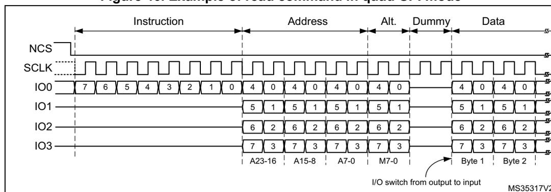
Instruction phase
During this phase, an 8-bit instruction, configured in INSTRUCTION bitfield of QUADSPI_CCR[7:0] register, is sent to the flash memory, specifying the type of operation to be performed.
Most flash memories can receive instructions only one bit at a time from the IO0/SO signal (single-SPI mode), the instruction phase can optionally send 2 bits at a time (over IO0/IO1 in dual-SPI mode), or 4 bits at a time (over IO0/IO1/IO2/IO3 in quad-SPI mode). This can be configured using the IMODE[1:0] bitfield of QUADSPI_CCR[9:8] register.
When IMODE = 00, the instruction phase is skipped, and the command sequence starts with the address phase, if present.
Address phase
In the address phase, 1-4 bytes are sent to the flash memory to indicate the address of the operation. The number of address bytes to be sent is configured in the ADSIZE[1:0] bitfield of QUADSPI_CCR[13:12] register. In indirect and automatic status-polling modes, address bytes to be sent are specified in the ADDRESS[31:0] bitfield of QUADSPI_AR register, while in memory-mapped mode, the address is given directly via the AHB (from the Cortex or from a DMA).
The address phase can send 1 bit at a time (over SO in single-SPI mode), 2 bits at a time (over IO0/IO1 in dual-SPI mode), or 4 bits at a time (over IO0/IO1/IO2/IO3 in quad-SPI mode). This can be configured using the ADMODE[1:0] bitfield of QUADSPI_CCR[11:10] register.
When ADMODE = 00, the address phase is skipped, and the command sequence proceeds directly to the next phase, if any.
Alternate-byte phase
In the alternate-byte phase, 1-4 bytes are sent to the flash memory, generally to control the mode of operation. The number of alternate bytes to be sent is configured in the [1:0] bitfield of QUADSPI_CCR[17:16] register. The bytes to be sent are specified in the QUADSPI_ABR register.
The alternate-bytes phase can send 1 bit at a time (over SO in single-SPI mode), 2 bits at a time (over IO0/IO1 in dual-SPI mode), or 4 bits at a time (over IO0/IO1/IO2/IO3 in quad-SPI mode). This can be configured using the ABMODE[1:0] bitfield of QUADSPI_CCR[15:14] register.
When ABMODE = 00, the alternate-byte phase is skipped, and the command sequence proceeds directly to the next phase, if any.
There may be times when only a single nibble needs to be sent during the alternate-byte phase rather than a full byte, such as when the dual-mode is used and only two cycles are used for the alternate bytes. In this case, the firmware can use quad-mode (ABMODE = 11) and send a byte with bits 7 and 3 of ALTERNATE set to 1 (keeping the IO3 line high), and bits 6 and 2 set to 0 (keeping the IO2 line low). In this case, the upper two bits of the nibble to be sent are placed in bits 4:3 of ALTERNATE, while the lower two bits are placed in bits 1 and 0. For example, if the nibble 2 (0010) is to be sent over IO0/IO1, then ALTERNATE must be set to 0x8A (1000_1010).
Dummy-cycle phase
In the dummy-cycle phase, 1-31 cycles are given without any data being sent or received, in order to give time to the flash memory to prepare for the data phase when higher clock frequencies are used. The number of cycles given during this phase is specified in the DCYC[4:0] bitfield of QUADSPI_CCR[22:18] register. In both SDR and DDR modes, the duration is specified as a number of full CLK cycles.
When DCYC is zero, the dummy-cycles phase is skipped, and the command sequence proceeds directly to the data phase, if present.
The operating mode of the dummy-cycles phase is determined by DMODE.
In order to assure enough “turn-around” time for changing data signals from output mode to input mode, there must be at least one dummy cycle when using dual or quad mode to receive data from the flash memory.
Data phase
During the data phase, any number of bytes can be sent to, or received from the flash memory.
In indirect and automatic status-polling modes, the number of bytes to be sent/received is specified in the QUADSPI_DLR register.
In indirect-write mode the data to be sent to the flash memory must be written to the QUADSPI_DR register. In indirect-read mode the data received from the flash memory is obtained by reading the QUADSPI_DR register.
In memory-mapped mode, the data which is read is sent back directly over the AHB to the Cortex or to a DMA.
The data phase can send/receive 1 bit at a time (over SO/SI in single-SPI mode), 2 bits at a time (over IO0/IO1 in dual-SPI mode), or 4 bits at a time (over IO0/IO1/IO2/IO3 in quad-SPI mode). This can be configured using the ABMODE[1:0] bitfield of QUADSPI_CCR[15:14] register.
When DMODE = 00, the data phase is skipped, and the command sequence finishes immediately by raising NCS. This configuration must only be used in only indirect write mode.
18.3.4 QUADSPI signal interface protocol modes
Single-SPI mode
This legacy SPI mode allows just one single bit to be sent/received serially. In this mode, data are sent to the flash memory over the SO signal (whose I/O shared with IO0). Data received from the flash memory arrive via SI (whose I/O shared with IO1).
The different phases can each be configured separately to use this mode by setting the IMODE/ADMODE/ABMODE/DMODE fields (in QUADSPI_CCR) to 01.
In each phase which is configured in single-SPI mode:
- • IO0 (SO) is in output mode.
- • IO1 (SI) is in input mode (high impedance).
- • IO2 is in output mode and forced to 0.
- • IO3 is in output mode and forced to 1 (to deactivate the “hold” function).
This is the case even for the dummy phase if DMODE = 01.
Dual-SPI mode
In dual-SPI mode, two bits are sent/received simultaneously over the IO0/IO1 signals.
The different phases can each be configured separately to use dual-SPI mode by setting the IMODE/ADMODE/ABMODE/DMODE fields of QUADSPI_CCR register to 10.
In each phase which is configured in dual-SPI mode:
- • IO0/IO1 are at high-impedance (input) during the data phase for read operations, and outputs in all other cases.
- • IO2 is in output mode and forced to 0.
- • IO3 is in output mode and forced to 1.
In the dummy phase when DMODE = 01, IO0/IO1 are always high-impedance.
Quad-SPI mode
In quad-SPI mode, four bits are sent/received simultaneously over the IO0/IO1/IO2/IO3 signals.
The different phases can each be configured separately to use quad-SPI mode by setting the IMODE/ADMODE/ABMODE/DMODE fields of QUADSPI_CCR register to 11.
In each phase which is configured in this mode, IO0/IO1/IO2/IO3 are all at high-impedance (input) during the data phase for read operations, and outputs in all other cases.
In the dummy phase when DMODE = 11, IO0/IO1/IO2/IO3 are all high-impedance.
IO2 and IO3 are used only in quad-SPI mode. If none of the phases are configured to use quad-SPI mode, then the pins corresponding to IO2 and IO3 can be used for other functions even while the QUADSPI is active.
SDR mode
By default, the DDRM bit (QUADSPI_CCR[31]) is 0 and the QUADSPI operates in single-data rate (SDR) mode.
In SDR mode, when the QUADSPI drives IO0/SO, IO1, IO2, IO3 signals, these signals transition only with the falling edge of CLK.
When receiving data in SDR mode, the QUADSPI assumes that flash memories also send the data using CLK falling edge. By default (when SSHIFT = 0), the signals are sampled using the following (rising) edge of CLK.
DDR mode
When the DDRM bit (QUADSPI_CCR[31]) is set to 1, the QUADSPI operates in double-data rate (DDR) mode.
In DDR mode, when the QUADSPI is driving the IO0/SO, IO1, IO2, IO3 signals in the address/alternate-byte/data phases, a bit is sent on each of CLK falling and rising edges.
The instruction phase is not affected by DDRM. The instruction is always sent using CLK falling edge.
When receiving data in DDR mode, the QUADSPI assumes that flash memories also send the data using both CLK rising and falling edges. When DDRM = 1, the firmware must clear SSHIFT (bit 4 of QUADSPI_CR). Thus, the signals are sampled one half of a CLK cycle later (on the following, opposite edge).
Figure 47. Example of a DDR command in quad-SPI mode
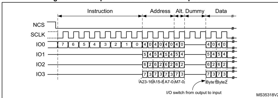
The diagram illustrates the timing for a DDR command in quad-SPI mode. It shows the following phases: Instruction, Address, Alt. Dummy, and Data. The Address phase is split into two 8-bit bytes: A23-16 and A15-8. The Data phase shows Byte 1 and Byte 2 being transferred. An arrow indicates the I/O switch from output to input between the Address and Alt. Dummy phases. The diagram is labeled MS35318V2.
18.3.5 QUADSPI indirect mode
When in indirect mode, commands are started by writing to QUADSPI registers, and data are transferred by writing or reading the data register, in the same way as for other communication peripherals.
When FMODE = 00 (QUADSPI_CCR[27:26]), the QUADSPI is in indirect-write mode, where bytes are sent to the flash memory during the data phase. Data are provided by writing to the data register (QUADSPI_DR).
When FMODE = 01, the QUADSPI is in indirect-read mode, where bytes are received from the flash memory during the data phase. Data are recovered by reading QUADSPI_DR.
The number of bytes to be read/written is specified in the data length register (QUADSPI_DLR). If QUADSPI_DLR = 0xFFFF_FFFF (all 1s), then the data length is considered undefined and the QUADSPI simply continues to transfer data until the end of flash memory (as defined by FSIZE) is reached. If no bytes are to be transferred, DMODE (QUADSPI_CCR[25:24]) must be set to 00.
If QUADSPI_DLR = 0xFFFF_FFFF and FSIZE = 0x1F (max value indicating a 4-Gbyte flash memory), then in this special case, transfers continue indefinitely, stopping only after an abort request or after the QUADSPI is disabled. After the last memory address is read (at address 0xFFFF_FFFF), reading continues with address = 0x0000_0000.
When the programmed number of bytes to be transmitted or received is reached, TCF is set and an interrupt is generated if TCIE = 1. In the case of undefined number of data, the TCF is set when the limit of the external SPI memory is reached according to the flash memory size defined in QUADSPI_CR.
Triggering the start of a command
Essentially, a command starts as soon as firmware gives the last information that is necessary for this command. Depending on the QUADSPI configuration, there are three different ways to trigger the start of a command in indirect mode. The commands starts immediately:
- • after a write is performed to INSTRUCTION[7:0] (QUADSPI_CCR), if no address is necessary (when ADMODE = 00) and if no data needs to be provided by the firmware (when FMODE = 01 or DMODE = 00)
- • after a write is performed to ADDRESS[31:0] (QUADSPI_AR), if an address is necessary (when ADMODE \( \neq \) 00) and if no data needs to be provided by the firmware (when FMODE = 01 or DMODE = 00)
- • after a write is performed to DATA[31:0] (QUADSPI_DR), if data needs to be provided by the firmware (when FMODE = 00 and DMODE \( \neq \) 00)
Writes to the alternate byte register (QUADSPI_ABR) never trigger the communication start. If alternate bytes are required, they must be programmed before.
As soon as a command is started, BUSY (bit 5 of QUADSPI_SR) is automatically set.
FIFO and data management
In indirect mode, data go through a 32-byte FIFO which is internal to the QUADSPI. FLEVEL[5:0] (QUADSPI_SR[13:8]) indicates how many bytes are currently being held in the FIFO.
In indirect-write mode (FMODE = 00), the firmware adds data to the FIFO when it writes QUADSPI_DR. Word writes add 4 bytes to the FIFO, halfword writes add 2 bytes, and byte writes add only 1 byte. If the firmware adds too many bytes to the FIFO (more than is indicated by DL[31:0]), the extra bytes are flushed from the FIFO at the end of the write operation (when TCF is set).
Byte/halfword accesses to QUADSPI_DR must be done only to the least significant byte/halfword of the 32-bit register.
FTHRES[4:0] is used to define a FIFO threshold. When the threshold is reached, FTF (FIFO threshold flag) is set. In indirect-read mode, FTF is set when the number of valid bytes to be read from the FIFO is above the threshold. FTF is also set if there are data in the FIFO after the last byte is read from the flash memory, regardless of the FTHRES setting. In indirect-write mode, FTF is set when the number of empty bytes in the FIFO is above the threshold.
If FTIE = 1, there is an interrupt when FTF is set. If DMAEN = 1, a DMA transfer is initiated when FTF is set. FTF is cleared by hardware as soon as the threshold condition is no longer true (after enough data is transferred by the CPU or DMA).
18.3.6 QUADSPI automatic status-polling mode
In automatic status-polling mode, the QUADSPI periodically starts a command to read a defined number of status bytes (up to 4). The received bytes can be masked to isolate some status bits and an interrupt can be generated when the selected bits have a defined value.
Accesses to the flash memory begin in the same way as in indirect-read mode: if no address is required (AMODE = 00), accesses begin as soon as the QUADSPI_CCR is written.
Otherwise, if an address is required, the first access begins when QUADSPI_AR is written. BUSY goes high at this point and stays high even between the periodic accesses.
The contents of MASK[31:0] (QUADSPI_PSMAR) are used to mask the data from the flash memory in automatic status-polling mode. If MASK[n] = 0, then bit n of the result is masked and not considered. If MASK[n] = 1, and the content of bit[n] is the same as MATCH[n] (QUADSPI_PSMAR), then there is a match for bit n.
If the polling match mode bit (PMM, bit 23 of QUADSPI_CR) is 0, then “AND” match mode is activated. This means status match flag (SMF) is set only when there is a match on all of the unmasked bits.
If PMM = 1, then “OR” match mode is activated. This means SMF is set if there is a match on any of the unmasked bits.
An interrupt is called when SMF is set if SMIE = 1.
If the automatic status-polling mode stop (APMS) bit is set, the operation stops and BUSY goes to 0 as soon as a match is detected. Otherwise, BUSY stays at 1, and the periodic accesses continue until there is an abort or the QUADSPI is disabled (EN = 0).
The data register (QUADSPI_DR) contains the latest received status bytes (the FIFO is deactivated). The content of the data register is not affected by the masking used in the matching logic. The FTF status bit is set as soon as a new reading of the status is complete, and FTF is cleared as soon as the data is read.
18.3.7 QUADSPI memory-mapped mode
When configured in memory-mapped mode, the external SPI device is seen as an internal memory.
It is forbidden to access the quad-SPI flash bank area before having properly configured and enabled the QUADSPI peripheral.
No more than 256 Mbytes can be addressed even if the flash memory capacity is larger.
If an access is made to an address outside of the range defined by FSIZE but still within the 256-Mbyte range, then a bus error is given. The effect of this error depends on the bus master that attempted the access:
- • If it is the Cortex CPU, bus fault exception is generated when enabled (or an HardFault exception when bus fault is disabled).
- • If it is a DMA, a DMA transfer error is generated and the corresponding DMA channel is automatically disabled.
Byte, halfword, and word access types are all supported.
Support for execute in place (XIP) operation is implemented, where the QUADSPI anticipates the next access and load in advance the byte at the following address. If the subsequent access is indeed made at a continuous address, the access is completed faster since the value is already prefetched.
By default, the QUADSPI never stops its prefetch operation, keeping the previous read operation active with NCS maintained low, even if no access to the flash memory occurs for a long time. Since flash memories tend to consume more when NCS is held low, the application may want to activate the timeout counter (TCEN = 1, bit 3 of QUADSPI_CR) so that NCS is released after a period of TIMEOUT[15:0] (QUADSPI_LPTR) cycles have elapsed without any access since when the FIFO becomes full with prefetch data.
BUSY goes high as soon as the first memory-mapped access occurs. Because of the prefetch operations, BUSY does not fall until there is a timeout, there is an abort, or the peripheral is disabled.
18.3.8 QUADSPI flash memory configuration
The device configuration register (QUADSPI_DCR) can be used to specify the characteristics of the external SPI flash memory.
The FSIZE[4:0] bitfield defines the size of external memory using the following formula:
FSIZE+1 is effectively the number of address bits required to address the flash memory. The flash memory capacity can be up to 4 Gbytes (addressed using 32 bits) in indirect mode, but the addressable space in memory-mapped mode is limited to 256 Mbytes.
When the QUADSPI executes two commands, one immediately after the other, it raises NCS high between the two commands for only one CLK cycle by default. If the flash memory requires more time between commands, the CSHT bitfield can be used to specify the minimum number of CLK cycles (up to 8) that NCS must remain high.
The clock mode (CKMODE) bit indicates the CLK signal logic level in between commands (when NCS = 1).
18.3.9 QUADSPI delayed data sampling
By default, the QUADSPI samples the data driven by the flash memory one half of a CLK cycle after the flash memory drives the signal.
In case of external signal delays, it may be beneficial to sample the data later. Using SSHIFT (bit 4 of QUADSPI_CR), the sampling of the data can be shifted by half of a CLK cycle.
Clock shifting is not supported in DDR mode: SSHIFT must be clear when DDRM bit is set.
18.3.10 QUADSPI configuration
The QUADSPI configuration is done in two phases:
- 1. QUADSPI peripheral configuration
- 2. QUADSPI flash memory configuration
Once configured and enabled, the QUADSPI can be used in one of its three operating modes: indirect, automatic status-polling, or memory-mapped mode.
QUADSPI configuration
The QUADSPI is configured using QUADSPI_CR. The user must configure the clock prescaler division factor and the sample shifting settings for the incoming data.
The DDR mode can be set through the DDRM bit. When setting the quad-SPI interface in DDR mode, the internal divider of kernel clock must be set with a division ratio of two or more. Once enabled, the address and the alternate bytes are sent on both clock edges, and the data are sent/received on both clock edges. Regardless of the DDRM bit setting, instructions are always sent in SDR mode.
DMA requests are enabled setting the DMAEN bit. In case of interrupt usage, their respective enable bit can be also set during this phase.
The FIFO level for either DMA request generation or interrupt generation is programmed in the FTHRES bits.
If a timeout counter is needed, the TCEN bit can be set and the timeout value programmed in the QUADSPI_LPTR register.
QUADSPI flash memory configuration
The parameters related to the targeted external flash memory are configured through the QUADSPI_DCR register. The user must program the flash memory size in the FSIZE bits, the chip-select minimum high time in CSHT bits, and the functional mode (Mode 0 or Mode 3) in the MODE bit.
18.3.11 QUADSPI use
The operating mode is selected using FMODE[1:0] (QUADSPI_CCR[27:26]).
Indirect mode
When FMODE is programmed to 00, the indirect-write mode is selected and data can be sent to the flash memory. With FMODE = 01, the indirect-read mode is selected where data can be read from the flash memory.
When the QUADSPI is used in indirect mode, the frames are constructed in the following way:
- 1. Specify a number of data bytes to read or write in QUADSPI_DLR.
- 2. Specify the frame format, mode and instruction code in QUADSPI_CCR.
- 3. Specify optional alternate byte to be sent right after the address phase in QUADSPI_ABR.
- 4. Specify the operating mode in QUADSPI_CR. If FMODE = 00 (indirect-write mode) and DMAEN = 1, then QUADSPI_AR must be specified before QUADSPI_CR. Otherwise QUADSPI_DR can be written by the DMA before QUADSPI_AR is updated (if the DMA controller has already been enabled).
- 5. Specify the targeted address in QUADSPI_AR.
- 6. Read/write the data from/to the FIFO through QUADSPI_DR.
When writing QUADSPI_CR, the user specifies the following settings:
- • enable bit (EN) set to 1
- • DMA enable bit (DMAEN) for transferring data to/from RAM
- • timeout counter enable bit (TCEN)
- • sample shift setting (SSHIFT)
- • FIFO threshold level (FTRHES) to indicate when the FTF flag must be set
- • interrupt enables
- • automatic status-polling mode parameters: match mode and stop mode (valid when FMODE = 11)
- • clock prescaler
When writing QUADSPI_CCR, the user specifies the following parameters:
- • instruction byte through INSTRUCTION bits
- • the way the instruction has to be sent through the IMODE bits (1/2/4 lines)
- • the way the address has to be sent through the ADMODE bits (None/1/2/4 lines)
- • address size (8/16/24/32-bit) through ADSIZE bits
- • the way the alternate bytes have to be sent through the ABMODE (None/1/2/4 lines)
- • alternate bytes number (1/2/3/4) through the ABSIZE bits
- • presence or not of dummy bytes through the DBMODE bit
- • number of dummy bytes through the DCYC bits
- • the way data have to be sent/received (none/1/2/4 lines) through DMODE bits
If neither QUADSPI_AR nor QUADSPI_DR need to be updated for a particular command, then the command sequence starts as soon as QUADSPI_CCR is written. This is the case when both ADMODE and DMODE are 00, or if just ADMODE = 00 when in indirect read mode (FMODE = 01).
When an address is required (ADMODE is not 00) and the data register does not need to be written (when FMODE = 01 or DMODE = 00), the command sequence starts as soon as the address is updated with a write to QUADSPI_AR.
In case of data transmission (FMODE = 00 and DMODE != 00), the communication start is triggered by a write in the FIFO through QUADSPI_DR.
Automatic status-polling mode
This mode is enabled setting the FMODE bitfield (QUADSPI_CCR[27:26]) to 10. In this mode, the programmed frame is sent and the data retrieved periodically.
The maximum amount of data read in each frame is 4 bytes. If more data is requested in QUADSPI_DLR, it is ignored and only 4 bytes are read.
The periodicity is specified in the QUADSPI_PISR register.
Once the status data is retrieved, it can internally be processed:
- • to set the status match flag and generate an interrupt if enabled
- • to stop automatically the periodic retrieving of the status bytes
The received value can be masked with the value stored in QUADSPI_PSMKR and ORed or ANDed with the value stored in QUADSPI_PSMAR.
In case of match, the status match flag is set and an interrupt is generated if enabled, and the QUADSPI can be automatically stopped if the AMPS bit is set.
In any case, the latest retrieved value is available in QUADSPI_DR.
Memory-mapped mode
In memory-mapped mode, the external flash memory is seen as an internal memory but with some latency during accesses. Only read operations are allowed to the external flash memory in this mode.
The memory-mapped mode is entered by setting FMODE to 11 in QUADSPI_CCR.
The programmed instruction and frame is sent when a master is accessing the memory-mapped space.
The FIFO is used as a prefetch buffer to anticipate linear reads. Any access to QUADSPI_DR in this mode returns zero.
QUADSPI_DLR has no meaning in memory-mapped mode.
18.3.12 Sending the instruction only once
Some flash memories (for example: Winbound) provide a mode where an instruction must be sent only with the first command sequence, while subsequent commands start directly with the address. One can take advantage of such a feature using the SIOO bit (QUADSPI_CCR[28]).
SIOO is valid for all functional modes (indirect, automatic status-polling, and memory-mapped). If the SIOO bit is set, the instruction is sent only for the first command following a write to QUADSPI_CCR. Subsequent command sequences skip the instruction phase, until there is a write to QUADSPI_CCR.
SIOO has no effect when IMODE = 00 (no instruction).
18.3.13 QUADSPI error management
An error can be generated in the following case:
- • In indirect mode or automatic status-polling mode when a wrong address is programmed in QUADSPI_AR (according to the flash memory size defined by FSIZE[4:0] in the QUADSPI_DCR), TEF is set and an interrupt is generated if enabled.
Also in indirect mode, if the address plus the data length exceeds the flash memory size, TEF is set as soon as the access is triggered.
- • In memory-mapped mode, when an out-of-range access is done by a master or when the QUADSPI is disabled, a bus error is generated as a response to the faulty bus master request.
When a master is accessing the memory mapped space while the memory-mapped mode is disabled, a bus error is generated as a response to the faulty bus master request.
18.3.14 QUADSPI busy bit and abort functionality
Once the QUADSPI starts an operation with the flash memory, the BUSY bit is automatically set in QUADSPI_SR.
In indirect mode, BUSY is reset once the QUADSPI has completed the requested command sequence, and the FIFO is empty.
In automatic status-polling mode, BUSY goes low only after the last periodic access is complete, due to a match when APMS = 1, or due to an abort.
After the first access in memory-mapped mode, BUSY goes low only on a timeout event or on an abort.
Any operation can be aborted by setting the ABORT bit in QUADSPI_CR. Once the abort is completed, BUSY and ABORT are automatically reset, and the FIFO is flushed.
Note: Some flash memories may misbehave if a write operation to a status registers is aborted.
18.3.15 NCS behavior
By default, NCS is high, deselecting the external flash memory. NCS falls before an operation begins and rises as soon as it finishes.
When CKMODE = 0 (“mode0”, where CLK stays low when no operation is in progress), NCS falls one CLK cycle before an operation first rising CLK edge, and NCS rises one CLK cycle after the operation final rising CLK edge, as shown in the figure below.
Figure 48. NCS when CKMODE = 0 (T = CLK period)
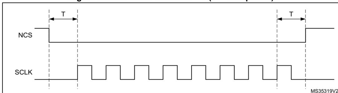
Timing diagram showing NCS (top) and SCLK (bottom) signals. NCS is active-low. The diagram shows NCS falling one CLK cycle before the first rising edge of SCLK and rising one CLK cycle after the last rising edge of SCLK. The period T is indicated between two rising edges of SCLK. The diagram is labeled MS35319V2.
When CKMODE=1 (“mode3”, where CLK goes high when no operation is in progress) and DDRM=0 (SDR mode), NCS still falls one CLK cycle before an operation first rising CLK edge, and NCS rises one CLK cycle after the operation final rising CLK edge, as shown in the figure below.
Figure 49. NCS when CKMODE = 1 in SDR mode (T = CLK period)
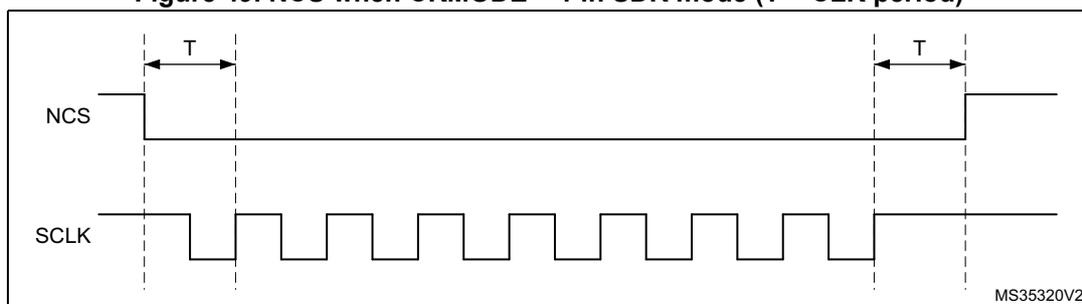
Timing diagram showing NCS (top) and SCLK (bottom) signals. NCS is active-low. The diagram shows NCS falling one CLK cycle before the first rising edge of SCLK and rising one CLK cycle after the last rising edge of SCLK. The period T is indicated between two rising edges of SCLK. The diagram is labeled MS35320V2.
When CKMODE = 1 (“mode3”) and DDRM = 1 (DDR mode), NCS falls one CLK cycle before an operation first rising CLK edge, and NCS rises one CLK cycle after the operation final active rising CLK edge, as shown in the figure below. Because DDR operations must finish with a falling edge, CLK is low when NCS rises, and CLK rises back up one half of a CLK cycle afterwards.
Figure 50. NCS when CKMODE = 1 in DDR mode (T = CLK period)
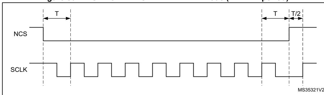
Timing diagram showing NCS (top) and SCLK (bottom) signals. NCS is active-low. The diagram shows NCS falling one CLK cycle before the first rising edge of SCLK and rising one CLK cycle after the last active rising edge of SCLK. The period T is indicated between two rising edges of SCLK. The time from the last active rising edge of SCLK to the rising edge of NCS is T/2. The diagram is labeled MS35321V2.
When the FIFO stays full in a read operation or if the FIFO stays empty in a write operation, the operation stalls and CLK stays low until firmware services the FIFO. If an abort occurs when an operation is stalled, NCS rises just after the abort is requested and then CLK rises one half of a CLK cycle later, as shown in Figure 51 .
Figure 51. NCS when CKMODE = 1 with an abort (T = CLK period)
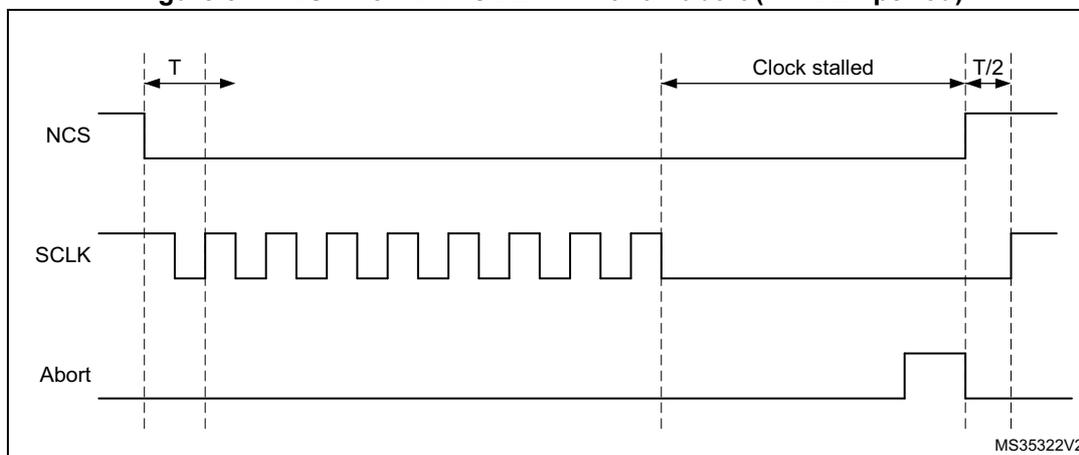
The diagram illustrates the timing relationship between NCS, SCLK, and an Abort signal. NCS (Active Low) is shown as a signal that goes high when an abort occurs. SCLK is a square wave that is held low during a 'Clock stalled' period. The 'Abort' signal goes high at a certain point. Following the abort, NCS rises immediately, and SCLK rises one half of a CLK cycle (T/2) later. The clock period is labeled T.
18.4 QUADSPI interrupts
An interrupt can be produced on the following events:
- • Timeout
- • Status match
- • FIFO threshold
- • Transfer complete
- • Transfer error
Separate interrupt enable bits are available for flexibility.
Table 85. QUADSPI interrupt requests
| Interrupt event | Event flag | Enable control bit |
|---|---|---|
| Timeout | TOF | TOIE |
| Status match | SMF | SMIE |
| FIFO threshold | FTF | FTIE |
| Transfer complete | TCF | TCIE |
| Transfer error | TEF | TEIE |
18.5 QUADSPI registers
18.5.1 QUADSPI control register (QUADSPI_CR)
Address offset: 0x000
Reset value: 0x0000 0000
| 31 | 30 | 29 | 28 | 27 | 26 | 25 | 24 | 23 | 22 | 21 | 20 | 19 | 18 | 17 | 16 |
|---|---|---|---|---|---|---|---|---|---|---|---|---|---|---|---|
| PRESCALER[7:0] | PMM | APMS | Res. | TOIE | SMIE | FTIE | TCIE | TEIE | |||||||
| rw | rw | rw | rw | rw | rw | rw | rw | rw | rw | rw | rw | rw | rw | rw | |
| 15 | 14 | 13 | 12 | 11 | 10 | 9 | 8 | 7 | 6 | 5 | 4 | 3 | 2 | 1 | 0 |
| Res. | Res. | Res. | FTHRES[4:0] | Res. | Res. | Res. | SSHIFT | TCEN | DMAEN | ABORT | EN | ||||
| rw | rw | rw | rw | rw | rw | rw | rw | rw | rw | ||||||
Bits 31:24 PRESCALER[7:0] : Clock prescaler
This bitfield defines the scaler factor for generating CLK based on the clock (value+1).
0: \( F_{CLK} = F \) , clock used directly as QUADSPI CLK (prescaler bypassed)
1: \( F_{CLK} = F/2 \)
2: \( F_{CLK} = F/3 \)
...
255: \( F_{CLK} = F/256 \)
For odd clock division factors, CLK duty cycle is not 50%. The clock signal remains low one cycle longer than it stays high.
When setting quad-SPI interface in DDR mode, the prescaler must be set with a division ratio of two or more.
Note: This bitfield can be modified only when BUSY = 0.
Bit 23 PMM : Polling match mode
This bit indicates which method must be used for determining a “match” during automatic status-polling mode.
0: AND match mode. SMF is set if all the unmasked bits received from the flash memory match the corresponding bits in the match register.
1: OR match mode. SMF is set if any one of the unmasked bits received from the flash memory matches its corresponding bit in the match register.
Note: This bit can be modified only when BUSY = 0.
Bit 22 APMS : Automatic status-polling mode stop
This bit determines if automatic status-polling is stopped after a match.
0: Automatic status-polling mode is stopped only by abort or by disabling the QUADSPI.
1: Automatic status-polling mode stops as soon as there is a match.
Note: This bit can be modified only when BUSY = 0.
Bit 21 Reserved, must be kept at reset value.
Bit 20 TOIE : Timeout interrupt enable
This bit enables the timeout interrupt.
0: Interrupt disabled
1: Interrupt enabled
Bit 19 SMIE : Status match interrupt enable
This bit enables the status match interrupt.
0: Interrupt disabled
1: Interrupt enabled
Bit 18 FTIE : FIFO threshold interrupt enable
This bit enables the FIFO threshold interrupt.
0: Interrupt disabled
1: Interrupt enabled
Bit 17 TCIE : Transfer complete interrupt enable
This bit enables the transfer complete interrupt.
0: Interrupt disabled
1: Interrupt enabled
Bit 16 TEIE : Transfer error interrupt enable
This bit enables the transfer error interrupt.
0: Interrupt disabled
1: Interrupt enabled
Bits 15:13 Reserved, must be kept at reset value.
Bits 12:8 FTHRES[4:0] : FIFO threshold level
This bitfield defines, in indirect mode, the threshold number of bytes in the FIFO that causes the FIFO threshold flag (bit FTF in register QUADSPI_SR) to be set.
0: In indirect-write mode (FMODE = 00), FTF is set if there are one or more free bytes location left in the FIFO, or indirect-read mode (FMODE = 01), FTF is set if there are one or more valid bytes that can be read from the FIFO.
1: In indirect-write mode (FMODE = 00), FTF is set if there are two or more free bytes location left in the FIFO, or indirect-read mode (FMODE = 01), FTF is set if there are two or more valid bytes that can be read from the FIFO
...
31: In indirect-write mode (FMODE = 00), FTF is set if there are 32 free bytes location left in the FIFO, or indirect-read mode (FMODE = 01), FTF is set if there are 32 valid bytes that can be read from the FIFO.
If DMAEN = 1, then the DMA controller for the corresponding channel must be disabled before changing the FTHRES value.
Bits 7:5 Reserved, must be kept at reset value.
Bit 4 SSHIFT : Sample shift
By default, when SSHIFT = 0, the QUADSPI samples data on the following CLK edge after the data is driven by the flash memory.
When SSHIFT = 1, an additional data sampling delay is introduced. In this case, the data is sampled on the next clock edge to accommodate external signal delays.
0: No shift
1: Shift to the next CLK edge
The firmware must ensure that SSHIFT = 0 when operating in DDR mode (DDRM = 1).
Note: This bitfield can only be modified when BUSY = 0.
Bit 3 TCEN : Timeout counter enableThis bit is valid only when memory-mapped mode (FMODE = 11) is selected. Activating this bit causes the NCS to be released (and thus reduces consumption) if there has not been an access after a certain amount of time, where this time is defined by TIMEOUT[15:0] (QUADSPI_LPTR). This bit enables the timeout counter.
By default, the QUADSPI never stops its prefetch operation, keeping the previous read operation active with NCS maintained low, even if no access to the flash memory occurs for a long time. Since flash memories tend to consume more when NCS is held low, the application may want to activate the timeout counter (TCEN = 1, bit 3 of QUADSPI_CR) so that NCS is released after a period of TIMEOUT[15:0] (QUADSPI_LPTR) cycles have elapsed without an access since when the FIFO becomes full with prefetch data.
0: Timeout counter is disabled, and thus the NCS remains active indefinitely after an access in memory-mapped mode.
1: Timeout counter is enabled, and thus the NCS is released in memory-mapped mode after TIMEOUT[15:0] cycles of flash memory inactivity.
Note: This bit can be modified only when BUSY = 0.
Bit 2 DMAEN : DMA enableIn indirect mode, the DMA can be used to input or output data via the QUADSPI_DR register. DMA transfers are initiated when the FIFO threshold flag, FTF, is set.
0: DMA is disabled for indirect mode.
1: DMA is enabled for indirect mode.
Bit 1 ABORT : Abort requestThis bit aborts the ongoing command sequence. It is automatically reset once the abort is complete. This bit stops the current transfer.
In automatic status-polling or memory-mapped mode, this bit also reset APM or DM bit.
0: No abort requested
1: Abort requested
Bit 0 EN : QUADSPI enable0: QUADSPI disabled
1: QUADSPI enabled
18.5.2 QUADSPI device configuration register (QUADSPI_DCR)
Address offset: 0x004
Reset value: 0x0000 0000
| 31 | 30 | 29 | 28 | 27 | 26 | 25 | 24 | 23 | 22 | 21 | 20 | 19 | 18 | 17 | 16 |
|---|---|---|---|---|---|---|---|---|---|---|---|---|---|---|---|
| Res. | Res. | Res. | Res. | Res. | Res. | Res. | Res. | Res. | Res. | Res. | FSIZE[4:0] | ||||
| rw | rw | rw | rw | rw | |||||||||||
| 15 | 14 | 13 | 12 | 11 | 10 | 9 | 8 | 7 | 6 | 5 | 4 | 3 | 2 | 1 | 0 |
| Res. | Res. | Res. | Res. | Res. | CSHT[2:0] | Res. | Res. | Res. | Res. | Res. | CKMO DE | ||||
| rw | rw | rw | rw | ||||||||||||
Bits 31:21 Reserved, must be kept at reset value.
Bits 20:16 FSIZE[4:0] : Flash memory size
This bitfield defines the size of external memory using the following formula:
Number of bytes in flash memory = \( 2^{[\text{FSIZE}+1]} \)
FSIZE+1 is effectively the number of address bits required to address the flash memory.
The flash memory capacity can be up to 4 Gbytes (addressed using 32 bits) in indirect mode, but the addressable space in memory-mapped mode is limited to 256 Mbytes.
Note: This bitfield can be modified only when BUSY = 0.
Bits 15:11 Reserved, must be kept at reset value.
Bits 10:8 CSHT[2:0] : Chip select high time
CSHT+1 defines the minimum number of CLK cycles which the chip select (NCS) must remain high between commands issued to the flash memory.
0: NCS stays high for at least 1 cycle between flash memory commands
1: NCS stays high for at least 2 cycles between flash memory commands
...
7: NCS stays high for at least 8 cycles between flash memory commands
Note: This bitfield can be modified only when BUSY = 0.
Bits 7:1 Reserved, must be kept at reset value.
Bit 0 CKMODE : Mode 0/mode 3
This bit indicates the level that CLK takes between commands (when NCS = 1).
0: CLK must stay low while NCS is high (chip select released). This is referred to as mode 0.
1: CLK must stay high while NCS is high (chip select released). This is referred to as mode 3.
Note: This bitfield can be modified only when BUSY = 0.
18.5.3 QUADSPI status register (QUADSPI_SR)
Address offset: 0x008
Reset value: 0x0000 0000
| 31 | 30 | 29 | 28 | 27 | 26 | 25 | 24 | 23 | 22 | 21 | 20 | 19 | 18 | 17 | 16 |
|---|---|---|---|---|---|---|---|---|---|---|---|---|---|---|---|
| Res. | Res. | Res. | Res. | Res. | Res. | Res. | Res. | Res. | Res. | Res. | Res. | Res. | Res. | Res. | Res. |
| 15 | 14 | 13 | 12 | 11 | 10 | 9 | 8 | 7 | 6 | 5 | 4 | 3 | 2 | 1 | 0 |
| Res. | Res. | FLEVEL[5:0] | Res. | Res. | BUSY | TOF | SMF | FTF | TCF | TEF | |||||
| r | r | r | r | r | r | r | r | r | r | r | r | ||||
Bits 31:14 Reserved, must be kept at reset value.
Bits 13:8 FLEVEL[5:0] : FIFO level
This bitfield gives the number of valid bytes which are being held in the FIFO. FLEVEL = 0 when the FIFO is empty, and 32 when it is full. In memory-mapped mode and in automatic status-polling mode, FLEVEL is zero.
Bits 7:6 Reserved, must be kept at reset value.
Bit 5 BUSY : Busy
This bit is set when an operation is on going. This bit clears automatically when the operation with the flash memory is finished and the FIFO is empty.
Bit 4 TOF : Timeout flag
This bit is set when timeout occurs. It is cleared by writing 1 to CTOF.
Bit 3 SMF : Status match flag
This bit is set in automatic status-polling mode when the unmasked received data matches the corresponding bits in the match register (QUADSPI_PSMAR). It is cleared by writing 1 to CSMF.
Bit 2 FTF : FIFO threshold flag
In indirect mode, this bit is set when the FIFO threshold is reached, or if there is any data left in the FIFO after reads from the flash memory are complete. It is cleared automatically as soon as threshold condition is no longer true.
In automatic status-polling mode this bit is set every time the status register is read, and the bit is cleared when the data register is read.
Bit 1 TCF : Transfer complete flag
This bit is set in indirect mode when the programmed number of data is transferred or in any mode when the transfer is aborted. It is cleared by writing 1 to CTCF.
Bit 0 TEF : Transfer error flag
This bit is set in indirect mode when an invalid address is being accessed in indirect mode. It is cleared by writing 1 to CTEF.
18.5.4 QUADSPI flag clear register (QUADSPI_FCR)
Address offset: 0x00C
Reset value: 0x0000 0000
| 31 | 30 | 29 | 28 | 27 | 26 | 25 | 24 | 23 | 22 | 21 | 20 | 19 | 18 | 17 | 16 |
|---|---|---|---|---|---|---|---|---|---|---|---|---|---|---|---|
| Res. | Res. | Res. | Res. | Res. | Res. | Res. | Res. | Res. | Res. | Res. | Res. | Res. | Res. | Res. | Res. |
| 15 | 14 | 13 | 12 | 11 | 10 | 9 | 8 | 7 | 6 | 5 | 4 | 3 | 2 | 1 | 0 |
| Res. | Res. | Res. | Res. | Res. | Res. | Res. | Res. | Res. | Res. | Res. | CTOF | CSMF | Res. | CTCF | CTEF |
| w | w | w | w |
Bits 31:5 Reserved, must be kept at reset value.
Bit 4 CTOF : Clear timeout flag
Writing 1 clears the TOF flag in QUADSPI_SR.
Bit 3 CSMF : Clear status match flag
Writing 1 clears the SMF flag in QUADSPI_SR.
Bit 2 Reserved, must be kept at reset value.
Bit 1 CTCF : Clear transfer complete flag
Writing 1 clears the TCF flag in QUADSPI_SR.
Bit 0 CTEF : Clear transfer error flag
Writing 1 clears the TEF flag in QUADSPI_SR.
18.5.5 QUADSPI data length register (QUADSPI_DLR)
Address offset: 0x010
Reset value: 0x0000 0000
| 31 | 30 | 29 | 28 | 27 | 26 | 25 | 24 | 23 | 22 | 21 | 20 | 19 | 18 | 17 | 16 |
|---|---|---|---|---|---|---|---|---|---|---|---|---|---|---|---|
| DL[31:16] | |||||||||||||||
| rw | rw | rw | rw | rw | rw | rw | rw | rw | rw | rw | rw | rw | rw | rw | rw |
| 15 | 14 | 13 | 12 | 11 | 10 | 9 | 8 | 7 | 6 | 5 | 4 | 3 | 2 | 1 | 0 |
| DL[15:0] | |||||||||||||||
| rw | rw | rw | rw | rw | rw | rw | rw | rw | rw | rw | rw | rw | rw | rw | rw |
Bits 31:0 DL[31:0] : Data length
Number of data to be retrieved (value+1) in indirect and automatic status-polling modes.
A value no greater than 3 (indicating 4 bytes) must be used for automatic status-polling mode.
All 1s in indirect mode means undefined length, where the QUADSPI continues until the end of memory, as defined by FSIZE.
0x0000_0000: 1 byte is to be transferred
0x0000_0001: 2 bytes are to be transferred
0x0000_0002: 3 bytes are to be transferred
0x0000_0003: 4 bytes are to be transferred
...
0xFFFF_FFFD: 4,294,967,294 (4G-2) bytes are to be transferred
0xFFFF_FFFE: 4,294,967,295 (4G-1) bytes are to be transferred
0xFFFF_FFFF: undefined length -- all bytes until the end of flash memory (as defined by FSIZE) are to be transferred. Continue reading indefinitely if FSIZE = 0x1F.
This bitfield has no effect when it is in memory-mapped mode (FMODE = 11).
Note: This bitfield can be written only when BUSY = 0.
18.5.6 QUADSPI communication configuration register (QUADSPI_CCR)
Address offset: 0x014
Reset value: 0x0000 0000
| 31 | 30 | 29 | 28 | 27 | 26 | 25 | 24 | 23 | 22 | 21 | 20 | 19 | 18 | 17 | 16 |
|---|---|---|---|---|---|---|---|---|---|---|---|---|---|---|---|
| DDRM | Res. | Res. | SIOO | FMODE[1:0] | DMODE[1:0] | Res. | DCYC[4:0] | ABSIZE[1:0] | |||||||
| rw | rw | rw | rw | rw | rw | rw | rw | rw | rw | rw | rw | rw | |||
| 15 | 14 | 13 | 12 | 11 | 10 | 9 | 8 | 7 | 6 | 5 | 4 | 3 | 2 | 1 | 0 |
| ABMODE[1:0] | ADSIZE[1:0] | ADMODE[1:0] | IMODE[1:0] | INSTRUCTION[7:0] | |||||||||||
| rw | rw | rw | rw | rw | rw | rw | rw | rw | rw | rw | rw | rw | rw | rw | rw |
Bit 31 DDRM : Double data rate mode
This bit sets the DDR mode for the address, alternate byte and data phase:
0: DDR mode disabled
1: DDR mode enabled
Note: This bit can be written only when BUSY = 0.
Bit 30 Reserved, must be kept at reset value.
Bit 29 Reserved, must be kept at reset value.
Bit 28 SIOO : Send instruction only once mode
This bit has no effect when IMODE = 00. See Section 18.3.12 for more details.
0: Instruction sent on every transaction
1: Instruction sent only for the first command
Note: This bit can be written only when BUSY = 0.
Bits 27:26 FMODE[1:0] : Functional mode
This bitfield defines the QUADSPI functional mode of operation.
00: Indirect-write mode
01: Indirect-read mode
10: Automatic status-polling mode
11: Memory-mapped mode
If DMAEN = 1 already, the DMA controller for the corresponding channel must be disabled before changing the FMODE value.
Note: This bitfield can be written only when BUSY = 0.
Bits 25:24 DMODE[1:0] : Data mode
This bitfield defines the data phase mode of operation:
00: No data
01: Data on a single line
10: Data on two lines
11: Data on four lines
This bitfield also determines the dummy phase mode of operation.
Note: This bitfield can be written only when BUSY = 0.
Bit 23 Reserved, must be kept at reset value.
Bits 22:18 DCYC[4:0] : Number of dummy cycles
This bitfield defines the duration of the dummy phase. In both SDR and DDR modes, it specifies a number of CLK cycles (0-31).
Note: This bitfield can be written only when BUSY = 0.
Bits 17:16 ABSIZE[1:0] : Alternate-byte size
This bit defines the size of alternate bytes.
00: 8-bit alternate byte
01: 16-bit alternate bytes
10: 24-bit alternate bytes
11: 32-bit alternate bytes
Note: This bitfield can be written only when BUSY = 0.
Bits 15:14 ABMODE[1:0] : Alternate byte mode
This bitfield defines the alternate-byte phase mode of operation.
00: No alternate bytes
01: Alternate bytes on a single line
10: Alternate bytes on two lines
11: Alternate bytes on four lines
Note: This bitfield can be written only when BUSY = 0.
Bits 13:12 ADSIZE[1:0] : Address size
This bit defines address size:
00: 8-bit address
01: 16-bit address
10: 24-bit address
11: 32-bit address
Note: This bitfield can be written only when BUSY = 0.
Bits 11:10 ADMODE[1:0] : Address mode
This bitfield defines the address phase mode of operation.
- 00: No address
- 01: Address on a single line
- 10: Address on two lines
- 11: Address on four lines
Note: This bitfield can be written only when BUSY = 0.
Bits 9:8 IMODE[1:0] : Instruction mode
This bitfield defines the instruction phase mode of operation.
- 00: No instruction
- 01: Instruction on a single line
- 10: Instruction on two lines
- 11: Instruction on four lines
Note: This bitfield can be written only when BUSY = 0.
Bits 7:0 INSTRUCTION[7:0] : Instruction
Instruction to be sent to the external SPI device.
Note: This bitfield can be written only when BUSY = 0.
18.5.7 QUADSPI address register (QUADSPI_AR)
Address offset: 0x018
Reset value: 0x0000 0000
| 31 | 30 | 29 | 28 | 27 | 26 | 25 | 24 | 23 | 22 | 21 | 20 | 19 | 18 | 17 | 16 |
|---|---|---|---|---|---|---|---|---|---|---|---|---|---|---|---|
| ADDRESS[31:16] | |||||||||||||||
| rw | rw | rw | rw | rw | rw | rw | rw | rw | rw | rw | rw | rw | rw | rw | rw |
| 15 | 14 | 13 | 12 | 11 | 10 | 9 | 8 | 7 | 6 | 5 | 4 | 3 | 2 | 1 | 0 |
| ADDRESS[15:0] | |||||||||||||||
| rw | rw | rw | rw | rw | rw | rw | rw | rw | rw | rw | rw | rw | rw | rw | rw |
Bits 31:0 ADDRESS[31:0] : Address
This bitfield contains the address to be sent to the external flash memory.
Writes to this bitfield are ignored when BUSY = 1 or when FMODE = 11 (memory-mapped mode).
18.5.8 QUADSPI alternate-byte register (QUADSPI_ABR)
Address offset: 0x01C
Reset value: 0x0000 0000
| 31 | 30 | 29 | 28 | 27 | 26 | 25 | 24 | 23 | 22 | 21 | 20 | 19 | 18 | 17 | 16 |
|---|---|---|---|---|---|---|---|---|---|---|---|---|---|---|---|
| ALTERNATE[31:16] | |||||||||||||||
| rw | rw | rw | rw | rw | rw | rw | rw | rw | rw | rw | rw | rw | rw | rw | rw |
| 15 | 14 | 13 | 12 | 11 | 10 | 9 | 8 | 7 | 6 | 5 | 4 | 3 | 2 | 1 | 0 |
| ALTERNATE[15:0] | |||||||||||||||
| rw | rw | rw | rw | rw | rw | rw | rw | rw | rw | rw | rw | rw | rw | rw | rw |
Bits 31:0 ALTERNATE[31:0] : Alternate bytes
Optional data to be sent to the external SPI device right after the address.
Note: This bitfield can be written only when BUSY = 0.
18.5.9 QUADSPI data register (QUADSPI_DR)
Address offset: 0x020
Reset value: 0x0000 0000
| 31 | 30 | 29 | 28 | 27 | 26 | 25 | 24 | 23 | 22 | 21 | 20 | 19 | 18 | 17 | 16 |
| DATA[31:16] | |||||||||||||||
| rw | rw | rw | rw | rw | rw | rw | rw | rw | rw | rw | rw | rw | rw | rw | rw |
| 15 | 14 | 13 | 12 | 11 | 10 | 9 | 8 | 7 | 6 | 5 | 4 | 3 | 2 | 1 | 0 |
| DATA[15:0] | |||||||||||||||
| rw | rw | rw | rw | rw | rw | rw | rw | rw | rw | rw | rw | rw | rw | rw | rw |
Bits 31:0 DATA[31:0] : Data
Data to be sent/received to/from the external SPI device.
In indirect write mode, data written to this register is stored on the FIFO before it is sent to the flash memory during the data phase. If the FIFO is too full, a write operation is stalled until the FIFO has enough space to accept the amount of data being written.
In indirect read mode, reading this register gives (via the FIFO) the data which was received from the flash memory. If the FIFO does not have as many bytes as requested by the read operation and if BUSY=1, the read operation is stalled until enough data is present or until the transfer is complete, whichever happens first.
In automatic status-polling mode, this register contains the last data read from the flash memory (without masking).
Word, halfword, and byte accesses to this register are supported. In indirect write mode, a byte write adds 1 byte to the FIFO, a halfword write 2, and a word write 4. Similarly, in indirect read mode, a byte read removes 1 byte from the FIFO, a halfword read 2, and a word read 4. Accesses in indirect mode must be aligned to the bottom of this register: a byte read must read DATA[7:0] and a halfword read must read DATA[15:0].
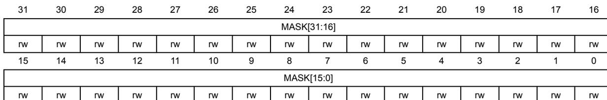
18.5.10 QUADSPI polling status mask register (QUADSPI_PSMKR)
Address offset: 0x024
Reset value: 0x0000 0000
| 31 | 30 | 29 | 28 | 27 | 26 | 25 | 24 | 23 | 22 | 21 | 20 | 19 | 18 | 17 | 16 |
| MASK[31:16] | |||||||||||||||
| rw | rw | rw | rw | rw | rw | rw | rw | rw | rw | rw | rw | rw | rw | rw | rw |
| 15 | 14 | 13 | 12 | 11 | 10 | 9 | 8 | 7 | 6 | 5 | 4 | 3 | 2 | 1 | 0 |
| MASK[15:0] | |||||||||||||||
| rw | rw | rw | rw | rw | rw | rw | rw | rw | rw | rw | rw | rw | rw | rw | rw |
Bits 31:0 MASK[31:0] : Status mask
Mask to be applied to the status bytes received in automatic status-polling mode.
For bit n:
0: Bit n of the data received in automatic status-polling mode is masked and its value is not considered in the matching logic
1: Bit n of the data received in automatic status-polling mode is unmasked and its value is considered in the matching logic
Note: This bitfield can be written only when BUSY = 0.
18.5.11 QUADSPI polling status match register (QUADSPI_PSMAR)
Address offset: 0x028
Reset value: 0x0000 0000
| 31 | 30 | 29 | 28 | 27 | 26 | 25 | 24 | 23 | 22 | 21 | 20 | 19 | 18 | 17 | 16 |
|---|---|---|---|---|---|---|---|---|---|---|---|---|---|---|---|
| MATCH[31:16] | |||||||||||||||
| rw | rw | rw | rw | rw | rw | rw | rw | rw | rw | rw | rw | rw | rw | rw | rw |
| 15 | 14 | 13 | 12 | 11 | 10 | 9 | 8 | 7 | 6 | 5 | 4 | 3 | 2 | 1 | 0 |
| MATCH[15:0] | |||||||||||||||
| rw | rw | rw | rw | rw | rw | rw | rw | rw | rw | rw | rw | rw | rw | rw | rw |
Bits 31:0 MATCH[31:0] : Status match
Value to be compared with the masked status register to get a match.
Note: This bitfield can be written only when BUSY = 0.
18.5.12 QUADSPI polling interval register (QUADSPI_PIR)
Address offset: 0x02C
Reset value: 0x0000 0000
| 31 | 30 | 29 | 28 | 27 | 26 | 25 | 24 | 23 | 22 | 21 | 20 | 19 | 18 | 17 | 16 |
|---|---|---|---|---|---|---|---|---|---|---|---|---|---|---|---|
| Res. | Res. | Res. | Res. | Res. | Res. | Res. | Res. | Res. | Res. | Res. | Res. | Res. | Res. | Res. | Res. |
| 15 | 14 | 13 | 12 | 11 | 10 | 9 | 8 | 7 | 6 | 5 | 4 | 3 | 2 | 1 | 0 |
| INTERVAL[15:0] | |||||||||||||||
| rw | rw | rw | rw | rw | rw | rw | rw | rw | rw | rw | rw | rw | rw | rw | rw |
Bits 31:16 Reserved, must be kept at reset value.
Bits 15:0 INTERVAL[15:0] : Polling interval
Number of CLK cycles between two read during automatic status-polling phases.
Note: This bitfield can be written only when BUSY = 0.
18.5.13 QUADSPI low-power timeout register (QUADSPI_LPTR)
Address offset: 0x030
Reset value: 0x0000 0000
| 31 | 30 | 29 | 28 | 27 | 26 | 25 | 24 | 23 | 22 | 21 | 20 | 19 | 18 | 17 | 16 |
|---|---|---|---|---|---|---|---|---|---|---|---|---|---|---|---|
| Res. | Res. | Res. | Res. | Res. | Res. | Res. | Res. | Res. | Res. | Res. | Res. | Res. | Res. | Res. | Res. |
| 15 | 14 | 13 | 12 | 11 | 10 | 9 | 8 | 7 | 6 | 5 | 4 | 3 | 2 | 1 | 0 |
| TIMEOUT[15:0] | |||||||||||||||
| rw | rw | rw | rw | rw | rw | rw | rw | rw | rw | rw | rw | rw | rw | rw | rw |
Bits 31:16 Reserved, must be kept at reset value.
Bits 15:0 TIMEOUT[15:0] : Timeout period
After each access in memory-mapped mode, the QUADSPI prefetches the subsequent bytes and holds these bytes in the FIFO. This bitfield indicates how many CLK cycles the QUADSPI waits after the FIFO becomes full until it raises NCS, putting the flash memory in a lower-consumption state.
Note: This bitfield can be written only when BUSY = 0.
18.5.14 QUADSPI register map
Table 86. QUADSPI register map and reset values
| Offset | Register name | 31 | 30 | 29 | 28 | 27 | 26 | 25 | 24 | 23 | 22 | 21 | 20 | 19 | 18 | 17 | 16 | 15 | 14 | 13 | 12 | 11 | 10 | 9 | 8 | 7 | 6 | 5 | 4 | 3 | 2 | 1 | 0 | |
|---|---|---|---|---|---|---|---|---|---|---|---|---|---|---|---|---|---|---|---|---|---|---|---|---|---|---|---|---|---|---|---|---|---|---|
| 0x000 | QUADSPI_CR | PRESCALER[7:0] | PMM | APMS | Res. | TOIE | SMIE | FTIE | TCIE | TEIE | Res. | Res. | Res. | FTHRES[4:0] | Res. | Res. | Res. | SSHIFT | TCEN | DMAEN | ABORT | EN | ||||||||||||
| Reset value | 0 | 0 | 0 | 0 | 0 | 0 | 0 | 0 | 0 | 0 | 0 | 0 | 0 | 0 | 0 | 0 | 0 | 0 | 0 | 0 | 0 | 0 | 0 | 0 | 0 | |||||||||
| 0x004 | QUADSPI_DCR | Res. | Res. | Res. | Res. | Res. | Res. | Res. | Res. | Res. | Res. | Res. | FSIZE[4:0] | Res. | Res. | Res. | Res. | Res. | CSHT | Res. | Res. | Res. | Res. | Res. | Res. | Res. | CKMODE | |||||||
| Reset value | 0 | 0 | 0 | 0 | 0 | 0 | 0 | 0 | 0 | |||||||||||||||||||||||||
| 0x008 | QUADSPI_SR | Res. | Res. | Res. | Res. | Res. | Res. | Res. | Res. | Res. | Res. | Res. | Res. | Res. | Res. | Res. | Res. | Res. | Res. | Res. | FLEVEL[5:0] | Res. | Res. | BUS | TOF | SMF | FTF | TCF | TEF | |||||
| Reset value | 0 | 0 | 0 | 0 | 0 | 0 | 0 | 0 | 0 | 0 | 0 | 0 | ||||||||||||||||||||||
| 0x00C | QUADSPI_FCR | Res. | Res. | Res. | Res. | Res. | Res. | Res. | Res. | Res. | Res. | Res. | Res. | Res. | Res. | Res. | Res. | Res. | Res. | Res. | Res. | Res. | Res. | Res. | Res. | Res. | Res. | Res. | CTOF | CSMF | Res. | CTCF | CTEF | |
| Reset value | 0 | 0 | 0 | 0 | ||||||||||||||||||||||||||||||
| 0x010 | QUADSPI_DLR | DL[31:0] | ||||||||||||||||||||||||||||||||
| Reset value | 0 | 0 | 0 | 0 | 0 | 0 | 0 | 0 | 0 | 0 | 0 | 0 | 0 | 0 | 0 | 0 | 0 | 0 | 0 | 0 | 0 | 0 | 0 | 0 | 0 | 0 | 0 | 0 | 0 | 0 | 0 | 0 | ||
| 0x014 | QUADSPI_CCR | DDRM | Res. | Res. | SIOO | FMODE [1:0] | DMODE [1:0] | Res. | Res. | DCYC[4:0] | ABSIZE [1:0] | ABMODE [1:0] | ADSIZE [1:0] | ADMODE [1:0] | IMODE [1:0] | INSTRUCTION[7:0] | ||||||||||||||||||
| Reset value | 0 | 0 | 0 | 0 | 0 | 0 | 0 | 0 | 0 | 0 | 0 | 0 | 0 | 0 | 0 | 0 | 0 | 0 | 0 | 0 | 0 | 0 | 0 | 0 | 0 | 0 | 0 | 0 | ||||||
| 0x018 | QUADSPI_AR | ADDRESS[31:0] | ||||||||||||||||||||||||||||||||
| Reset value | 0 | 0 | 0 | 0 | 0 | 0 | 0 | 0 | 0 | 0 | 0 | 0 | 0 | 0 | 0 | 0 | 0 | 0 | 0 | 0 | 0 | 0 | 0 | 0 | 0 | 0 | 0 | 0 | 0 | 0 | 0 | 0 | ||
| 0x01C | QUADSPI_ABR | ALTERNATE[31:0] | ||||||||||||||||||||||||||||||||
| Reset value | 0 | 0 | 0 | 0 | 0 | 0 | 0 | 0 | 0 | 0 | 0 | 0 | 0 | 0 | 0 | 0 | 0 | 0 | 0 | 0 | 0 | 0 | 0 | 0 | 0 | 0 | 0 | 0 | 0 | 0 | 0 | 0 | ||
| 0x020 | QUADSPI_DR | DATA[31:0] | ||||||||||||||||||||||||||||||||
| Reset value | 0 | 0 | 0 | 0 | 0 | 0 | 0 | 0 | 0 | 0 | 0 | 0 | 0 | 0 | 0 | 0 | 0 | 0 | 0 | 0 | 0 | 0 | 0 | 0 | 0 | 0 | 0 | 0 | 0 | 0 | 0 | 0 | ||
Table 86. QUADSPI register map and reset values (continued)
| Offset | Register name | 31 | 30 | 29 | 28 | 27 | 26 | 25 | 24 | 23 | 22 | 21 | 20 | 19 | 18 | 17 | 16 | 15 | 14 | 13 | 12 | 11 | 10 | 9 | 8 | 7 | 6 | 5 | 4 | 3 | 2 | 1 | 0 |
|---|---|---|---|---|---|---|---|---|---|---|---|---|---|---|---|---|---|---|---|---|---|---|---|---|---|---|---|---|---|---|---|---|---|
| 0x024 | QUADSPI_PSMKR | MASK[31:0] | |||||||||||||||||||||||||||||||
| Reset value | 0 | 0 | 0 | 0 | 0 | 0 | 0 | 0 | 0 | 0 | 0 | 0 | 0 | 0 | 0 | 0 | 0 | 0 | 0 | 0 | 0 | 0 | 0 | 0 | 0 | 0 | 0 | 0 | 0 | 0 | 0 | 0 | |
| 0x028 | QUADSPI_PSMAR | MATCH[31:0] | |||||||||||||||||||||||||||||||
| Reset value | 0 | 0 | 0 | 0 | 0 | 0 | 0 | 0 | 0 | 0 | 0 | 0 | 0 | 0 | 0 | 0 | 0 | 0 | 0 | 0 | 0 | 0 | 0 | 0 | 0 | 0 | 0 | 0 | 0 | 0 | 0 | 0 | |
| 0x02C | QUADSPI_PIR | Res | Res | Res | Res | Res | Res | Res | Res | Res | Res | Res | Res | Res | Res | Res | Res | INTERVAL[15:0] | |||||||||||||||
| Reset value | 0 | 0 | 0 | 0 | 0 | 0 | 0 | 0 | 0 | 0 | 0 | 0 | 0 | 0 | 0 | ||||||||||||||||||
| 0x030 | QUADSPI_LPTR | Res | Res | Res | Res | Res | Res | Res | Res | Res | Res | Res | Res | Res | Res | Res | Res | TIMEOUT[15:0] | |||||||||||||||
| Reset value | 0 | 0 | 0 | 0 | 0 | 0 | 0 | 0 | 0 | 0 | 0 | 0 | 0 | 0 | 0 | ||||||||||||||||||
Refer to Section 2.2 for the register boundary addresses.