5. Power control (PWR)
5.1 Power supplies
The devices require a \( V_{DD} \) operating voltage supply between 1.71 V and 3.6 V. Several independent supplies ( \( V_{DDSMPS} \) , \( V_{FBSMPS} \) , \( V_{DDA} \) , \( V_{DDRF} \) , \( V_{DDUSB} \) , \( V_{LCD} \) ) can be provided for specific peripherals:
- • \( V_{DD} = 1.71 \text{ V to } 3.6 \text{ V} \)
\( V_{DD} \) is the external power supply for the I/Os, the system analog blocks such as reset, power management, internal clocks and low power regulator. It is provided externally through VDD pins.
- • \( V_{DDSMPS} = 1.71 \text{ V to } 3.6 \text{ V} \)
\( V_{DDSMPS} \) is the external power supply for the SMPS step-down converter. It is provided externally through VDDSMPS supply pin, and must be connected to the same supply as \( V_{DD} \) .
- • \( V_{FBSMPS} = 1.40 \text{ V to } 3.6 \text{ V} \)
\( V_{FBSMPS} \) is the external power supply for the main and RF system regulators. It is provided externally through VFBSPS pin, and may be supplied through either the SMPS step-down converter or connected to the same supply as \( V_{DD} \) .
- • \( V_{DDA} = 1.62 \text{ V (ADCs/COMPs) to } 2.4 \text{ V (VREFBUF) to } 3.6 \text{ V} \)
\( V_{DDA} \) is the external analog power supply for A/D converters, D/A converters, voltage reference buffer, operational amplifiers and comparators. The \( V_{DDA} \) voltage level is independent from the \( V_{DD} \) voltage and must preferably be connected to \( V_{DD} \) when these peripherals are not used. Note that VREFBUF is available only on STM32WB55xx devices.
- • \( V_{DDRF} = 1.71 \text{ V to } 3.6 \text{ V} \)
\( V_{DDRF} \) is the external power supply for the Radio. It is provided externally through the VDDRF pin, and must be connected to the same supply as \( V_{DD} \) .
- • \( V_{DDUSB} = 3.0 \text{ V to } 3.6 \text{ V} \)
\( V_{DDUSB} \) is the external independent power supply for USB transceivers. The \( V_{DDUSB} \) voltage level is independent from the \( V_{DD} \) voltage and must preferably be connected to \( V_{DD} \) when the USB is not used.
- • \( V_{LCD} = 2.5 \text{ V to } 3.6 \text{ V} \) (available only on STM32WB55xx devices)
The LCD controller can be powered either externally through the VLCD pin, or internally from an internal voltage generated by the embedded step-up converter, which can generate a voltage up to 3.6 V if \( V_{DD} \) is higher than 2.0 V. VLCD is multiplexed with PC3, which can be used as GPIO when the LCD is not used.
- • \( V_{BAT} = 1.55 \text{ V to } 3.6 \text{ V} \)
\( V_{BAT} \) is the power supply for RTC, external clock 32 kHz oscillator and backup registers (through power switch) when \( V_{DD} \) is not present.
- • VREF-, VREF+ (available only on STM32WB55xx devices)
V REF+ is the input reference voltage for the ADC. It is also the output of the internal voltage reference buffer when enabled.
- – V DDA < 2 V: V REF+ must be equal to V DDA
- – V DDA ≥ 2 V: V REF+ must be between 2 V and V DDA
V REF+ can be grounded when ADC is not active.
The internal voltage reference buffer supports two output voltages, configured with VRS bit in the VREFBUF_CSR register:
- – V REF+ ≈ 2.048 V: this requires V DDA equal to or higher than 2.4 V
- – V REF+ ≈ 2.5 V: this requires V DDA equal to or higher than 2.8 V
VREF+ pin is not available on all packages, when not available it is internally bonded to VDDA. When the VREF+ is double-bonded with VDDA in a package, the internal voltage reference buffer is not available and must be kept disabled (refer to the datasheet for pinout descriptions).
During power up and power down, the following power sequence is required:
- • When V DD < 1 V the other power supplies (V DDA , V DDUSB and V LCD ) must remain below V DD + 0.3 V. During the power down V DD can temporarily become lower than the other supplies only if the energy provided to the MCU remains below 1 mJ. This allows the external decoupling capacitors to discharge with different time constants.
- • When V DD ≥ 1 V all power supplies become independent.
An embedded linear voltage regulator is used to supply the internal digital power V CORE . V CORE is the power supply for digital peripherals, SRAM1 and SRAM2. The flash memory is supplied by V CORE and V DD .
Figure 6. Power supply overview
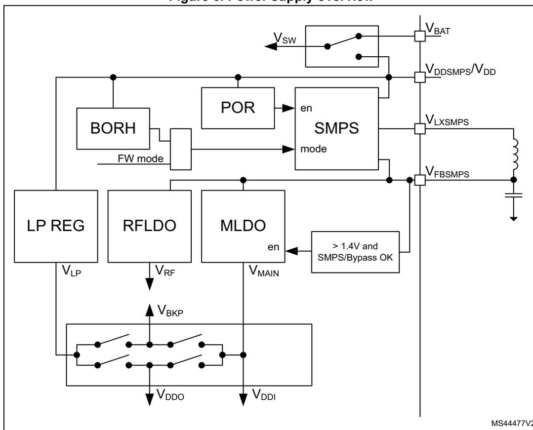
The diagram illustrates the internal power supply architecture. At the top, a switch connects the V SW pin to the V BAT pin. Below this, the V DDSMPS/V DD pin is connected to the SMPS block. The SMPS block has an 'en' input from the POR block and a 'mode' input from the BORH block. The BORH block has a 'FW mode' input. The SMPS block outputs V LXSMPS and V FBSMPS pins. V LXSMPS is connected to an inductor and a capacitor to ground. V FBSMPS is connected to a feedback network. The SMPS block also has an output V MAIN connected to the MLDO block. The MLDO block has an 'en' input from a > 1.4V and SMPS/Bypass OK block. The MLDO block outputs V MAIN pin. The LP REG block outputs V LP pin. The RFLDO block outputs V RF pin. The LP REG, RFLDO, and MLDO blocks are connected to a switch matrix. The switch matrix has inputs V LP , V RF , and V MAIN , and outputs V BKP , V DDO , and V DDI pins. The V BKP pin is connected to a battery. The V DDO and V DDI pins are connected to the external world. The diagram is labeled MS44477V2.
As shown in Figure 7, different supply configurations are supported, controlled according to the scheme of Table 19.
Figure 7. Supply configurations
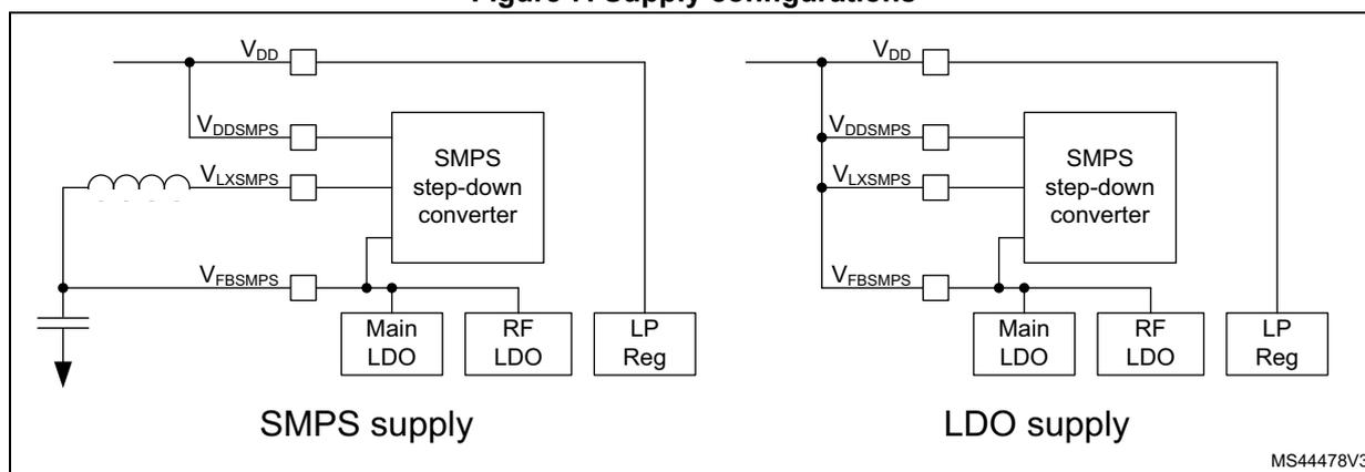
The diagram shows two supply configurations. On the left, labeled 'SMPS supply', the V DD pin is connected to the SMPS step-down converter. The SMPS block outputs V DDSMPS , V LXSMPS , and V FBSMPS pins. V DDSMPS is connected to the Main LDO, RF LDO, and LP Reg blocks. V LXSMPS is connected to an inductor and a capacitor to ground. V FBSMPS is connected to a feedback network. The Main LDO, RF LDO, and LP Reg blocks are connected to the SMPS block. On the right, labeled 'LDO supply', the V DD pin is connected directly to the Main LDO, RF LDO, and LP Reg blocks. The SMPS block is bypassed, and its outputs V DDSMPS , V LXSMPS , and V FBSMPS pins are not connected. The diagram is labeled MS44478V3.
The SMPS step-down converter operating mode depends upon the SMPSEN setting in PWR control register 5 (PWR_CR5) and upon the system operating modes Run, Stop0, Stop1, Stop2, Standby, and Shutdown.
Table 19. Supply configuration control
| Supply configuration | SMPSEN | System operating mode | Description |
|---|---|---|---|
| Default | 0 | NA | SMPS in Bypass mode |
| SMPS supply | 1 (1) | Run | SMPS in SMPS mode |
| Stop0 | |||
| Stop1 | SMPS in Open mode | ||
| Stop2 | |||
| Standby and Shutdown | |||
| LDO supply | 0 (2) | Any | SMPS in Bypass mode |
1. When SMPS step-down converter SMPS mode is enabled, it is good practice to enable the BORH to monitor the supply.
2. In LDO supply the SMPS must not be enabled, or the product can be permanently damaged.
Two specific features have been added to this step-down SMPS in association with the supported low power modes:
- • BYPASS mode: capability for the SMPS to be bypassed (the current continues to flow through its coil). The \( V_{DDSMPS} \) voltage is directly connected to \( V_{LXSMPS} \) . An additional hardware mechanism allows the SMPS to automatically switch to BYPASS mode if \( V_{DD} \) falls below a given level ( \( V_{BORH} \) ), ensuring smooth operation even at very low operating voltages.
- • OPEN mode: in this mode the SMPS output ( \( V_{LXSMPS} \) ) is open from any circuitry and the load of the SMPS bulk capacitance is kept. This makes it possible to speed up the wake-up time, by having the bulk capacitance precharged.
The internal state machine manages these states automatically when entering and exiting the low power modes.
After a POR reset the SMPS step-down converter is in Bypass mode.
During Stop1, Stop2, and Standby the SMPS step-down converter is put in the Open mode by hardware (see Table 19 ). When exiting from low-power modes (except Shutdown) the SMPS step-down converter is set by hardware to the mode selected by the SMPSEN bit (SMPS mode or Bypass). The SMPSEN bit in PWR control register 5 (PWR_CR5) is retained in Standby mode.
When the SMPS step-down converter is in SMPS mode the BORH can be configured, with BORHC in PWR control register 5 (PWR_CR5) , to enable switching on the fly when the supply drops below the SMPS step-down converter SMPS mode operating supply level. When the \( V_{DD} \) supply drops below the selected BORH threshold level the SMPS step-down converter is forced in Bypass mode, register bit SMPSEN is cleared. A SMPSFBF interrupt is generated when enabled. When the \( V_{DD} \) supply rises above the BORH threshold level, a BORHF interrupt is generated when enabled. It is up to the software to switch the SMPS step-down converter back to SMPS mode.
When the SMPS step-down converter is disabled SMPSEN is 0, the SMPS step-down converter is in Bypass mode and the application LDO mode can be used.
5.1.1 Independent analog peripherals supply
To improve ADC conversion accuracy and to extend the supply flexibility, the analog peripherals have an independent power supply that can be separately filtered and shielded from noise on the PCB.
- • The analog peripherals voltage supply input is available on a separate \( V_{DDA} \) pin.
- • An isolated supply ground connection is provided on \( V_{SSA} \) pin.
The \( V_{DDA} \) supply voltage can be different from \( V_{DD} \) . The presence of \( V_{DDA} \) must be checked before enabling any of the analog peripherals supplied by \( V_{DDA} \) (A/D converter, comparators, voltage reference buffer).
The \( V_{DDA} \) supply can be monitored by the Peripheral voltage monitoring, and compared with one threshold (1.65 V for PWM3), refer to Section 5.2.3 for more details.
When a single supply is used, \( V_{DDA} \) can be externally connected to \( V_{DD} \) through the external filtering circuit in order to ensure a noise-free \( V_{DDA} \) reference voltage.
The noise performance of analog signals may be impacted by the integrated SMPS switching. To prevent this the SMPS may be switched off on the fly when measuring analog signals.
ADC reference voltage (available only on STM32WB55xx)
To ensure a better accuracy on low-voltage inputs and outputs, the user can connect to \( V_{REF+} \) a separate reference voltage lower than \( V_{DDA} \) . \( V_{REF+} \) is the highest voltage, represented by the full scale value, for an analog input (ADC) signal.
\( V_{REF+} \) can be provided either by an external reference or by an internal buffered voltage reference (VREFBUF).
The internal voltage reference is enabled by setting the ENVR bit in the VREFBUF control and status register (VREFBUF_CSR) . The voltage reference is set to 2.5 V when the VRS bit is set and to 2.048 V when the VRS bit is cleared. The internal voltage reference can also provide the voltage to external components through \( V_{REF+} \) pin. Refer to the device datasheet and to Section 20: Voltage reference buffer (VREFBUF) for further information.
5.1.2 Independent USB transceivers supply
The USB transceivers are supplied from a separate \( V_{DDUSB} \) power supply pin. \( V_{DDUSB} \) range is from 3.0 V to 3.6 V and is completely independent from \( V_{DD} \) or \( V_{DDA} \) .
After reset, the USB features supplied by \( V_{DDUSB} \) are logically and electrically isolated and therefore are not available. The isolation must be removed before using the USB FS peripheral, by setting the USV bit in the PWR control register 2 (PWR_CR2) , once the \( V_{DDUSB} \) supply is present.
The \( V_{DDUSB} \) supply is monitored by the Peripheral voltage monitoring (PWM1) and compared with the internal reference voltage ( \( V_{REFINT} \sim 1.2 \) V), refer to Section 5.2.3 for more details.
5.1.3 Independent LCD supply (available only on STM32WB55xx)
The VLCD pin is provided to control the contrast of the glass LCD. This pin can be used in two ways:
- • it can receive from an external circuitry the desired maximum voltage that is provided
on segment and common lines to the glass LCD by the microcontroller
- • it can also be used to connect an external capacitor that is used by the microcontroller for its voltage step-up converter. This step-up converter is controlled by software to provide the desired voltage to segment and common lines of the glass LCD.
The voltage provided to segment and common lines defines the contrast of the glass LCD pixels. This contrast can be reduced when the user configures the dead time between frames.
- • When an external power supply is provided to the VLCD pin, it must be in the range from 2.5 V to 3.6 V. It does not depend on V DD .
- • When the LCD is based on the internal step-up converter, the VLCD pin should be connected to a capacitor (see the product datasheet for further information).
5.1.4 Battery backup domain
To retain the content of the Backup registers and supply the RTC function when V DD is turned off, the V BAT pin can be connected to an optional backup voltage supplied by a battery or by another source.
The V BAT pin powers the RTC unit, the LSE oscillator and the PC13 to PC15 I/Os, allowing the RTC to operate even when the main power supply is turned off. The switch to the V BAT supply is controlled by the power-down reset embedded in the Reset block.
Warning:
During
\(
t_{RSTTEMPO}
\)
(temporization at V
DD
startup) or after a PDR has been detected, the power switch between V
BAT
and V
DD
remains connected to V
BAT
.
During the startup phase, if V
DD
is established in less than
\(
t_{RSTTEMPO}
\)
(refer to the datasheet for its value) and
\(
V_{DD} > V_{BAT} + 0.6
\)
V, a current may be injected into V
BAT
through an internal diode connected between V
DD
and the power switch (V
BAT
).
If the power supply / battery connected to the V
BAT
pin cannot support this current injection, it is recommended to connect an external low-drop diode between this power supply and the V
BAT
pin.
If no external battery is used in the application, it is recommended to connect V BAT to V DD supply, and add a 100 nF external ceramic decoupling capacitor on V BAT pin.
When the backup domain is supplied by V DD (analog switch connected to V DD ), the following pins are available:
- • PC13 (STM32WB55xx only), PC14 and PC15, which can be used as GPIO pins
- • PC13 (STM32WB55xx only), PC14 and PC15, which can be configured by RTC or LSE (refer to Section 34.4: RTC functional description )
- • PA0/RTC_TAMP2 and PC12/RTC_TAMP3 (STM32WB55xx only) when configured by the RTC as tamper pins
Note: As the analog switch can transfer only a limited amount of current (3 mA), the use of GPIO PC13 to PC15 in output mode is restricted: the speed must be limited to 2 MHz with a
maximum load of 30 pF, and these I/Os cannot be used as current sources (e.g. to drive a LED).
When the backup domain is supplied by \( V_{BAT} \) (analog switch connected to \( V_{BAT} \) because \( V_{DD} \) is not present), the following functions are available:
- • PC13 (STM32WB55xx only), PC14 and PC15 can be controlled only by RTC or LSE (refer to Section 34.4: RTC functional description )
- • PA0/RTC_TAMP2 and PC12/RTC_TAMP3 (STM32WB55xx only) when configured by the RTC as tamper pins
Backup domain access
After a system reset, the backup domain (RTC registers and backup registers) is protected against possible unwanted write accesses. To enable access to the backup domain, set the DBP bit in the PWR control register 1 (PWR_CR1) to enable access to the backup domain.
VBAT battery charging
When \( V_{DD} \) is present, it is possible to charge the external battery on VBAT through an internal resistance.
The VBAT charging is done either through a 5 k \( \Omega \) resistor or through a 1.5 k \( \Omega \) resistor, depending upon the VBRS bit value in the PWR control register 4 (PWR_CR4) .
The battery charging is enabled by setting VBE bit in the PWR control register 4 (PWR_CR4) , and automatically disabled in VBAT mode.
5.1.5 Voltage regulator
Two embedded linear voltage regulators supply all the digital circuitries, except for the Standby circuitry and the backup domain. The main regulator output voltage ( \( V_{CORE} \) ) can be programmed by software to two different power ranges (Range 1 and Range 2) to optimize the consumption depending on the system maximum operating frequency (refer to Section 6.2.10: Clock source frequency versus voltage scaling and to Section 3.3.4: Read access latency ).
The voltage regulators are always enabled after a reset. Depending on the application modes, the \( V_{CORE} \) supply is provided either by the main regulator (MR) or by the low-power regulator (LPR).
- • In Run, Sleep and Stop0 modes, both regulators are enabled and the main regulator (MR) supplies full power to the \( V_{CORE} \) domain (core, memories and digital peripherals).
- • In low-power run and low-power sleep modes, the main regulator is off and the low-power regulator (LPR) supplies low power to the \( V_{CORE} \) domain, preserving the contents of the registers and internal SRAM1 and SRAM2.
- • In Stop1 and Stop2 modes the main regulator is off and the low-power regulator (LPR) supplies low power to the \( V_{CORE} \) domain, preserving the contents of the registers and of internal SRAM1 and SRAM2.
- • In Standby mode with SRAM2a content preserved (RRS bit is set in the PWR control register 3 (PWR_CR3) ), the main regulator (MR) is off and the low-power regulator (LPR) provides the supply to SRAM2a only. The core and digital peripherals (except Standby circuitry and backup domain), SRAM1 and SRAM2b are powered off.
- • In Standby mode, both regulators are powered off. The contents of the registers and of
SRAM1 and SRAM2 is lost except for the Standby circuitry and the backup domain.
- • In Shutdown mode, both regulators are powered off. When exiting from Shutdown mode, a power-on reset is generated. Consequently, the contents of the registers and of both SRAM1 and SRAM2 is lost, except for the backup domain.
5.1.6 Dynamic voltage scaling management
The dynamic voltage scaling is a power management technique that consists in increasing or decreasing the voltage used for the digital peripherals (V CORE ), according to the application performance and power consumption needs.
Dynamic voltage scaling to increase V CORE is known as “overvolting”, it is used to improve the device performance.
Dynamic voltage scaling to decrease V CORE is known as “undervolting”, performed to save power, particularly in laptop and other mobile devices where the energy comes from a battery and is thus limited.
- • Range 1: High-performance range
The main regulator provides a typical output voltage at 1.2 V. The system clock frequency can be up to 64 MHz. The Flash memory access time for read access is minimum, write and erase operations are possible.
- • Range 2: Low-power range
The main regulator provides a typical output voltage at 1.0 V. The system clock frequency can be up to 16 MHz. The Flash memory access time for a read access is increased as compared to Range 1; write and erase operations are possible.
Voltage scaling is selected through the VOS bit in the PWR control register 1 (PWR_CR1) .
The sequence to go from Range 1 to Range 2 is:
- 1. Reduce the system frequency to a value lower or equal to 16 MHz.
- 2. Adjust number of wait states according new frequency target in Range2 (LATENCY bits in the FLASH_ACR).
- 3. Select Range 2 in the VOS bits in the PWR control register 1 (PWR_CR1) .
The sequence to go from Range 2 to Range 1 is:
- 1. Select Range 1 in the VOS bits in the PWR control register 1 (PWR_CR1) .
- 2. Wait until the VOSF flag is cleared in the PWR status register 2 (PWR_SR2) .
- 3. Adjust number of wait states according new frequency target in Range1 (LATENCY bits in the FLASH_ACR).
- 4. Increase the system frequency.
5.2 Power supply supervisor
5.2.1 Power-on reset (POR) / power-down reset (PDR) / brown-out reset (BOR)
The device has an integrated power-on reset / power-down reset, coupled with a brown-out reset circuitry.
Five BOR thresholds can be selected through option bytes.
The BOR can be used in two operating modes, configured by the BORHC bit in PWR control register 5 (PWR_CR5) :
- • Reset mode, where a system reset is generated when the \( V_{DD} \) supply is below the selected BOR threshold.
- • Force SMPS step-down converter in Bypass mode when the \( V_{DD} \) supply is below the selected BOR threshold. When the \( V_{DD} \) supply is below the lowest BOR level a system reset is always generated.
The BOR is active in all power modes except Shutdown mode, and cannot be disabled. The BOR mechanism needs to be enabled, and can be disabled at any time if needed.
Reset mode
During power-on, the BOR keeps the device under reset until the supply voltage \( V_{DD} \) reaches the specified \( V_{BORx} \) threshold. When \( V_{DD} \) drops below the selected threshold, a device reset is generated. When \( V_{DD} \) is above the \( V_{BORx} \) upper limit, the device reset is released and the system can start.
Force SMPS step-down converter Bypass mode
During power-on, the BOR keeps the device under reset until the supply voltage \( V_{DD} \) reaches the specified \( V_{BORx} \) threshold. When \( V_{DD} \) drops below \( V_{BOR0} \) , a device reset is generated. When \( V_{DD} \) is above the \( V_{BORx} \) upper limit, the device reset is released and the system can start.
To enter and during the SMPS step-down converter in SMPS mode the selected \( BORx \) ( \( x = 1, 2, 3, 4 \) ) threshold is used to determine if SMPS mode is used or if the SMPS step-down converter is forced in Bypass mode. When \( V_{DD} \) drops below the selected threshold, the SMPS step-down converter when entering or in SMPS mode, is forced in Bypass mode. An SMPS step-down converter force Bypass interrupt (SMPSFBF) may be generated when enabled. When \( V_{DD} \) rises above the selected BOR upper limit, a BOR interrupt (BORHF) may be generated when enabled. It is up to software to set the SMPS step-down converter in SMPS mode.
For more details on the brown-out reset thresholds refer to the electrical characteristics section in the datasheet.
Figure 8. Brown-out reset waveform
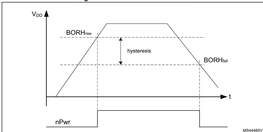
1. The reset temporization \( t_{RSTTEMPO} \) is present only for the BOR lowest threshold ( \( V_{BOR0} \) ).
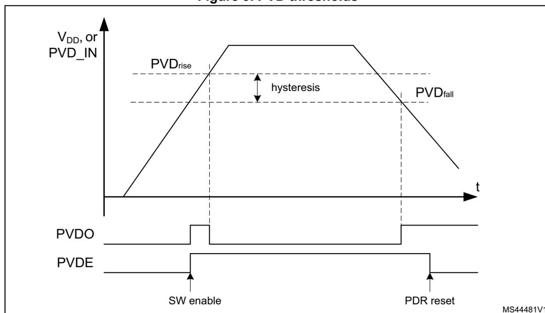
5.2.2 Programmable voltage detector (PVD)
The PVD can be used to monitor the \( V_{DD} \) power supply by comparing it to a threshold selected by the PLS[2:0] bits in the PWR control register 2 (PWR_CR2) .
The PVD can also be used to monitor a voltage level on the PVD_IN pin. In this case the voltage level on PVD_IN is compared to the internal VREFINT level.
The PVD is enabled by setting the PVDE bit.
A PVDO flag is available, in the PWR status register 2 (PWR_SR2) , to indicate if \( V_{DD} \) or the voltage level on PVD_IN is higher or lower than the PVD threshold. This event is internally connected to the EXTI Line16 and can generate an interrupt if enabled through the EXTI registers.
The PVD output interrupt can be generated when \( V_{DD} \) or the voltage level on PVD_IN drops below the PVD threshold, and/or when \( V_{DD} \) or the voltage level on PVD_IN rises above the PVD threshold, depending on EXTI Line16 rising/falling edge configuration. If the EXTI Line16 is configured to rising/falling edge sensitivity (rising/falling edge of PVDO), the interrupt is generated when \( V_{DD} \) or the voltage level on PVD_IN drops below/rises above the PVD threshold. As an example, the service routine can perform emergency shutdown tasks.
Figure 9. PVD thresholds
5.2.3 Peripheral voltage monitoring (PVM)
Only \( V_{DD} \) is monitored by default, as it is the only supply required for all system-related functions. The other supplies ( \( V_{DDA} \) and \( V_{DDUSB} \) ) can be independent from \( V_{DD} \) and can be monitored by the peripheral voltage monitoring (PVM).
Each PVM is a comparator between a fixed threshold \( V_{PVMx} \) and the selected power supply. PVMOx flags indicate if the independent power supply is higher or lower than the PVMx threshold: PVMOx flag is cleared when the supply voltage is above the PVMx threshold, and is set when the supply voltage is below the PVMx threshold.
Each PVM output is connected to an EXTI line and can generate an interrupt if enabled through the EXTI registers. The PVMx output interrupt is generated when the independent power supply drops below the PVMx threshold and/or when it rises above the PVMx threshold, depending on EXTI line rising/falling edge configuration.
Each PVM can remain active in Stop0, Stop1 and Stop2 modes, and the PVM interrupt can wake up from the Stop mode.
Table 20. PVM features
| PVM | Power supply | PVM threshold | EXTI line |
|---|---|---|---|
| PVM1 | \( V_{DDUSB} \) | \( V_{PVM1} \) (~ 1.2 V) | 31 |
| PVM2 | Not used | - | - |
| PVM3 | \( V_{DDA} \) | \( V_{PVM3} \) (~ 1.65 V) | 33 |
| PVM4 | Not used | - | - |
The independent supplies ( \( V_{DDA} \) and \( V_{DDUSB} \) ) are not considered as present by default, and a logical and electrical isolation is applied to ignore any information coming from the peripherals supplied by these dedicated sources.
- • If these supplies are shorted externally to \( V_{DD} \) , the application must assume that they are available without enabling any PVM.
- • If these supplies are independent from \( V_{DD} \) , the PVM can be enabled to confirm whether the supply is present or not.
The following sequence must be applied before using the USB_FS peripheral:
- 1. If
\(
V_{DDUSB}
\)
is independent from
\(
V_{DD}
\)
:
- a) Enable the PVM1 by setting PVME1 bit in the PWR control register 2 (PWR_CR2)
- b) Wait for the PVM1 wake-up time
- c) Wait until PVMO1 bit is cleared in the PWR status register 2 (PWR_SR2)
- d) Optional: Disable the PVM1 for consumption saving
- 2. Set the USV bit in the PWR control register 2 (PWR_CR2) to remove the \( V_{DDUSB} \) power isolation.
The following sequence must be applied before using analog to digital converters, digital to analog converters, comparators, operational amplifiers, voltage reference buffer:
- 1. If
\(
V_{DDA}
\)
is independent from
\(
V_{DD}
\)
:
- a) Enable the PVM3 by setting PVME3 bit in the PWR control register 2 (PWR_CR2)
- b) Wait for the PVM3 wake-up time
- c) Wait until PVMO3 bit is cleared in the PWR status register 2 (PWR_SR2)
- d) Optional: disable the PVM3 for consumption saving
- 2. Enable the analog peripheral, which automatically removes the \( V_{DDA} \) isolation.
5.3 CPU2 boot
Booting of the CPU2 is controlled by the C2BOOT bit in PWR control register 4 (PWR_CR4) register. This allows the CPU1 to initialize the system after a reset or wake-up from system Low-power mode, before booting the CPU2.
- • Following reset the CPU2 is prevented from booting by the C2BOOT bit. The CPU2 boots only once the CPU1 has set the C2BOOT bit.
- • When exiting from system low power modes STOP0, STOP1, STOP2 or STANDBY the C2BOOT bit controls the CPU2 booting.
- – When C2BOOT = 1, after a system low power mode the CPU2 boots when it is woken up via a wake-up source.
- – When C2BOOT = 0, after a system low power mode the CPU2 is prevented from booting. Instead on a CPU2 wake-up source the CPU1 is woken up via a C2HF. It is up to the CPU1 to boot the CPU2 by setting the C2BOOT bit.
Figure 10. CPU2 boot options
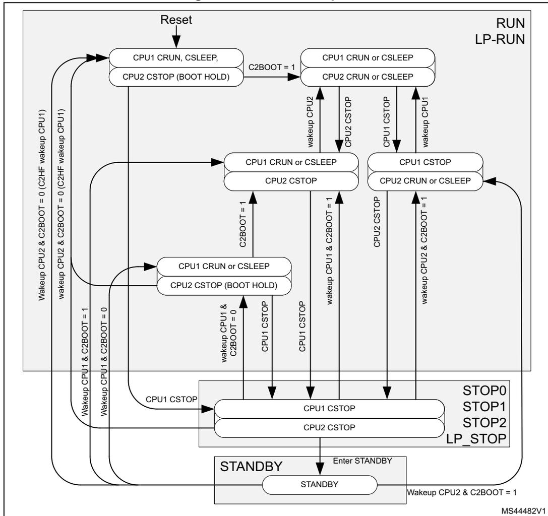
The diagram illustrates the boot options for CPU2 based on the state of CPU1 and the C2BOOT bit. It is divided into four main power modes: RUN, LP-RUN, STOP, and STANDBY.
- RUN / LP-RUN Mode:
- Initial State (after Reset): CPU1 is CRUN, CSLEEP; CPU2 is CSTOP (BOOT HOLD).
- Transition to Active State: If C2BOOT = 1, CPU1 becomes CRUN or CSLEEP, and CPU2 becomes CRUN or CSLEEP.
- From Active State: CPU1 can enter CSTOP, and CPU2 can enter CRUN or CSLEEP. CPU2 can also enter CSTOP.
- Wake-up Transitions:
- Wake-up CPU2 & C2BOOT = 0 (C2HF wake-up CPU1) leads to the Initial State.
- Wake-up CPU2 & C2BOOT = 0 (C2HF wake-up CPU1) leads to the Active State.
- Wake-up CPU1 & C2BOOT = 1 leads to the Initial State.
- Wake-up CPU1 & C2BOOT = 0 leads to the Active State.
- STOP0, STOP1, STOP2, LP_STOP Mode:
- Reached from RUN/LP-RUN via CPU1 CSTOP.
- From this mode, CPU1 can return to CRUN or CSLEEP, and CPU2 can return to CRUN or CSLEEP.
- Wake-up CPU1 & C2BOOT = 0 leads to the Active State.
- CPU1 CSTOP from this mode leads back to the STOP state.
- STANDBY Mode:
- Reached from STOP via "Enter STANDBY".
- From STANDBY, the system returns to the Initial State if Wake-up CPU2 & C2BOOT = 1.
MS44482V1
When the CPU2 is prevented from booting, the wake-up from Low-power mode boot procedure is the following:
- • Before the CPU1 enters CSTOP mode it clears the C2BOOT bit.
- • When CPU1 exits CSTOP:
- – When the system remains in Run mode, it sets the C2BOOT bit, and subsequently processes the wake-up event.
- – When the system exits from a low power mode from a CPU1 wake-up source, it initialize the system and sets the C2BOOT bit, and subsequently processes the wake-up event.
- – When the system exits from a low power mode from the C2HF wake-up source, it initializes the system and set the C2BOOT bit, and subsequently goes back to CSTOP.
- • There is no special wake-up procedure for the CPU2. When the CPU2 wakes up, the system has been initialized by the CPU1. So the CPU2 can directly process the wake-up event.
When the system remains in Run mode (due to the Radio system) the CPU2 wakes up from CSTOP mode independently from the C2BOOT setting.
5.4 Low-power modes
By default, the microcontroller is in Run mode after a system or a power Reset and at least one CPU is in CRun mode executing code. Low-power modes are available to save power when the CPU does not need to be kept running, for example when it is waiting for an external event. The user has to select the mode that gives the best compromise between consumption, startup time and available wake-up sources.
The individual CPUs feature two low power modes, entered by the CPU when executing WFI, WFE or on return from an exception handler when SLEEPONEXIT is enabled.
- • CSleep mode: when the CPU enters low power mode and SLEEPDEEP is disabled, Arm® “sleep mode”.
- • CStop mode: when the CPU enters low power mode and SLEEPDEEP is enabled, Arm® “sleepdeep mode”.
The device features several low-power modes:
- • Sleep mode : CPU clock off, all peripherals including CPU core peripherals (among them NVIC, SysTick) can run and wake up the CPU when an interrupt or an event occurs.
- • Low-power run mode (LP run) : This mode is achieved when the system clock frequency is reduced below 2 MHz. The code is executed from the SRAM or from the flash memory. The regulator is in low-power mode to minimize the operating current.
- • Low-power sleep mode (LP sleep) : This mode is entered from the Low-power run mode: CPU is off.
- • Stop0 mode, Stop1 mode and Stop2 mode : the content of SRAM1, SRAM2 and of all registers is retained. All clocks in the V CORE domain are stopped, the PLL, the MSI, the HSI16 and the HSE are disabled. The LSI and the LSE can be kept running.
The RTC can remain active (Stop mode with RTC, Stop mode without RTC).
Some peripherals with the wake-up capability can enable the HSI16 RC during Stop mode to detect their wake-up condition.
In Stop2 mode, most of the V CORE domain is put in a lower leakage mode. Stop1 offers the largest number of active peripherals and wake-up sources, a smaller wake-up time but a higher consumption compared with Stop2. In Stop0 mode, the main regulator remains ON, resulting in the fastest wake-up time, but with much higher consumption. The active peripherals and wake-up sources are the same as in Stop1 mode.
The system clock, when exiting from Stop0, Stop1 or Stop2 mode, can be either MSI up to 48 MHz or HSI16, depending on the software configuration.
- •
Standby mode
: V
CORE
domain is powered off. However, it is possible to preserve the SRAM2a contents:
- – Standby mode with SRAM2a retention when bit RRS is set in the PWR control register 3 (PWR_CR3) . In this case, SRAM2a is supplied by the low-power regulator.
- – Standby mode when bit RRS is cleared in the PWR control register 3 (PWR_CR3) .
In this case the main regulator and the low-power regulator are powered off.
All clocks in the \( V_{CORE} \) domain are stopped, the PLL, the MSI, the HSI16 and the HSE are disabled. The LSI and the LSE can be kept running.
The RTC can remain active (Standby mode with RTC, Standby mode without RTC).
The system clock, when exiting Standby modes, is HSI16.
- • Shutdown mode: \( V_{CORE} \) domain is powered off. All clocks in the \( V_{CORE} \) domain are stopped, the PLL, the MSI, the HSI16, the LSI and the HSE are disabled. The LSE can be kept running. The system clock, when exiting Shutdown mode, is MSI at 4 MHz. In this mode, the supply voltage monitoring is disabled and the product behavior is not guaranteed in case of a power voltage drop.
Note: Stop, Standby, and Shutdown modes are only entered when both CPUs are in CStop mode.
In addition, the power consumption in Run mode can be reduced by slowing down the system clocks, and/or by gating the clocks to the APB and AHB peripherals when they are unused.
The system operation mode depend on the CPU1, the CPU2 and the Radio sub-system operating mode. The system enters a low power mode only when all three sub-systems allow it to do so.
After a system reset the CPU1 is in CRUN mode. The CPU2 boots only if enabled by the CPU1 via the C2BOOT register bit. As long as the CPU1 does not boot the CPU2, the device operates as a single CPU system. The CPU1 can enter and wake up from system low power modes on its own.
When CPU2 has boot, the CPU1, CPU2 and Radio sub-systems can enter and wake up from system low power modes on their own. The different wake-up sources for the different sub-systems are detailed in Table 21 .
Table 21. Sub-system low power wake-up sources
| Wake-up source | CPU1 | CPU2 | Radio |
|---|---|---|---|
| EXTI | From Stop modes | From Stop modes | Not available |
| RTC | From Stop and Standby modes | From Stop and Standby modes | Not available |
| WKUP | From Stop and Standby modes | From Stop and Standby modes | Not available |
| SMPS | From Stop | From Stop | Not available |
| RADIO | From Stop | From Stop | Not available |
| RFWAKEUP | Not available | From Stop and Standby modes | From Stop and Standby modes |
The system low power mode to enter depends on the allowed mode selected by both CPUs in the LPMS bits of PWR control register 1 (PWR_CR1) and PWR CPU2 control register 1 (PWR_C2CR1) . This is also valid when CPU2 is kept in hold by C2BOOT.
Figure 11 shows the operating modes state diagram. The CPU1, CPU2 and Radio sub-systems operate interdependently, according to their own sub-system states. Each sub-system has its own wake-up sources, to wake up from Stop and Standby modes. For the device to be in Stop, Standby or Shutdown mode, all three sub-systems need to be in CStop. When one sub-system enters CRun mode, the device enters Run mode.
Figure 11. Low-power modes possible transitions
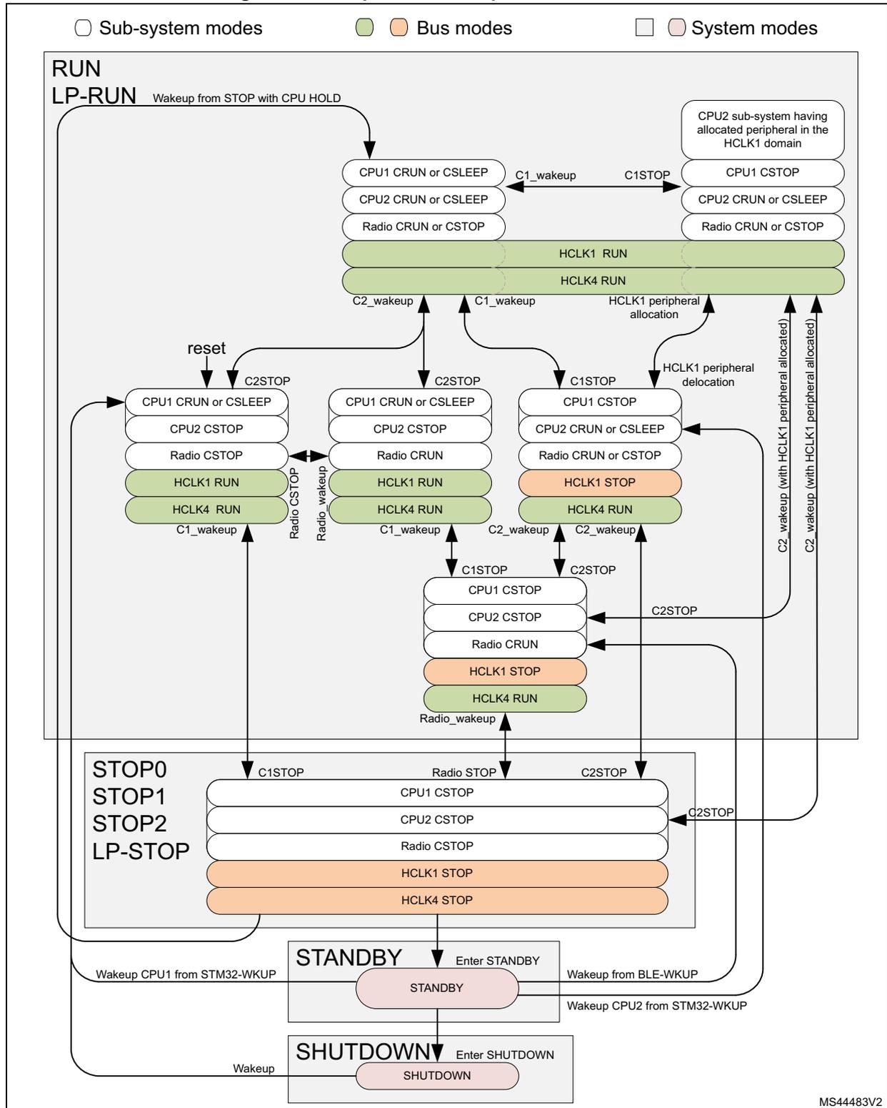
Legend:
- Sub-system modes
- Bus modes
- System modes
Power States:
- RUN / LP-RUN: Contains sub-system modes for CPU1, CPU2, and Radio, and bus modes HCLK1 and HCLK4. Transitions include 'Wakeup from STOP with CPU HOLD', 'reset', 'C1_wakeup', 'C2_wakeup', 'Radio_wakeup', and 'HCLK1 peripheral allocation/delocation'.
- STOP0 / STOP1 / STOP2 / LP-STOP: Contains sub-system modes for CPU1, CPU2, and Radio, and bus modes HCLK1 and HCLK4 in STOP state. Transitions include 'C1STOP', 'C2STOP', 'Radio STOP', and 'Enter STOP'.
- STANDBY: System mode with 'Enter STANDBY' and wake-up sources: 'Wake up CPU1 from STM32-WKUP', 'Wake up from BLE-WKUP', and 'Wake up CPU2 from STM32-WKUP'.
- SHUTDOWN: System mode with 'Enter SHUTDOWN' and 'Wake up' source.
MS44483V2
Table 22. Low-power mode summary
| Mode name | Entry | Wakeup source (1) | Wakeup system clock | Effect on clocks | Voltage regulator | |
|---|---|---|---|---|---|---|
| MR | LPR | |||||
| Sleep (Sleep-now or Sleep-on-exit) | WFI or Return from ISR | Any interrupt | Same as before entering Sleep mode | CPU clock OFF No effect on other clocks or analog clock sources | ON | |
| WFE | Wakeup event | |||||
| Low-power run | Set LPR bit | Clear LPR bit | Same as Low-power run clock | None | OFF | ON |
| Low-power sleep | Set LPR bit + WFI or Return from ISR | Any interrupt | Same as before entering Low-power sleep mode | CPU clock OFF No effect on other clocks or analog clock sources | ||
| Set LPR bit + WFE | Wakeup event | ON | ||||
| Stop0 | LPMS = "000" + SLEEPDEEP bit + WFI or Return from ISR or WFE | Any EXTI line (configured in the EXTI registers). Specific peripherals events | HSI16 when STOPWUCK = 1 in RCC_CFGR. MSI with the frequency before entering Stop mode when STOPWUCK = 0. | All clocks OFF except LSI and LSE | ||
| Stop1 | LPMS = "001" + SLEEPDEEP bit + WFI or Return from ISR or WFE | |||||
| Stop2 | LPMS = "010" + SLEEPDEEP bit + WFI or Return from ISR or WFE | OFF | ON | |||
| Standby with SRAM2a | LPMS = "011"+ Set RRS bit + SLEEPDEEP bit + WFI or Return from ISR or WFE | WKUP pin edge, RTC event, LSECSS, external reset in NRST pin, IWDG reset | HSI16 | |||
| Standby | LPMS = "011" + Clear RRS bit + SLEEPDEEP bit + WFI or Return from ISR or WFE | WKUP pin edge, RTC event, LSECSS, external reset in NRST pin, IWDG reset | OFF | OFF | ||
| Shutdown | LPMS = "1--" + SLEEPDEEP bit + WFI or Return from ISR or WFE | WKUP pin edge, RTC event, external reset in NRST pin | MSI 4 MHz | All clocks OFF except LSE | ||
Table 23. Functionalities depending on system operating mode (1)
| Peripheral | Run | Sleep | Low-power run | Low-power sleep | Stop0 | Stop1 | Stop2 | Standby | Shutdown | VBAT | |||||
|---|---|---|---|---|---|---|---|---|---|---|---|---|---|---|---|
| - | Wakeup capability | - | Wakeup capability | - | Wakeup capability | - | Wakeup capability | - | Wakeup capability | ||||||
| CPU1 | Y | - | Y | - | - | - | - | - | - | - | - | - | - | - | - |
| CPU2 | Y | - | Y | - | - | - | - | - | - | - | - | - | - | - | - |
| Radio-system (BLE, 802) | Y | Y | - | - | - | Y | - | Y | - | Y | - | Y (2) | - | - | - |
| Flash memory | Y | Y | O | O | R | - | R | - | R | - | R | - | R | - | R |
| SRAM1 | Y | O (4) | Y | O (4) | R | - | R | - | R | - | - | - | - | - | - |
| SRAM2a | Y | O (4) | Y | O (4) | R | - | R | - | R | - | O (3) | - | - | - | - |
| SRAM2b | Y | O (4) | Y | O (4) | R | - | R | - | R | - | - | - | - | - | - |
| QUADSPI | O | O | O | O | - | - | - | - | - | - | - | - | - | - | - |
| Backup registers | Y | Y | Y | Y | R | - | R | - | R | - | R | - | R | - | R |
| Brown-out reset (BOR) | Y | Y | Y | Y | Y | Y | Y | Y | Y | Y | Y | Y | - | - | - |
| Brown-out SMPS force bypass (BOR) | Y | Y | Y | Y | Y | Y | - | - | - | - | - | - | - | - | - |
| Programmable voltage detector (PVD) | O | O | O | O | O | O | O | O | O | O | - | - | - | - | - |
| Peripheral voltage monitor (PVMx; x=1, 3) | O | O | O | O | O | O | O | O | O | O | - | - | - | - | - |
| DMAx (x=1, 2) | O | O | O | O | - | - | - | - | - | - | - | - | - | - | - |
| High speed internal (HSI16) | O | O | O | O | O (5) | - | O (5) | - | - | - | - | - | - | - | - |
| Oscillator HSI48 | O | O | - | - | - | - | - | - | - | - | - | - | - | - | - |
| High speed external (HSE) | O | O | O | O | - | - | - | - | - | - | - | - | - | - | - |
| Low speed internal (LSI) | O | O | O | O | O | - | O | - | O | - | O | - | - | - | - |
| Low speed external (LSE) | O | O | O | O | O | - | O | - | O | - | O | - | O | - | O |
| Multi-speed internal (MSI) | O | O | O | O | - | - | - | - | - | - | - | - | - | - | - |
| Clock security system (CSS) | O | O | O | O | - | - | - | - | - | - | - | - | - | - | - |
| Clock security system on LSE | O | O | O | O | O | O | O | O | O | O | O | O | - | - | - |
| RTC / Auto wake-up | O | O | O | O | O | O | O | O | O | O | O | O | O | O | O |
| Number of RTC tamper pins | 3 | 3 | 3 | 3 | 3 | O | 3 | O | 3 | O | 3 | O | 3 | O | 3 |
| LCD (6) | O | O | O | O | O | O | O | O | O | O | - | - | - | - | - |
| USB FS | O (7) | O (7) | - | - | - | O | - | O | - | - | - | - | - | - | - |
| USART1 | O | O | O | O | O (8) | O (8) | O (8) | O (8) | - | - | - | - | - | - | - |
| Low-power UART (LPUART) | O | O | O | O | O (8) | O (8) | O (8) | O (8) | O (8) | O (8) | - | - | - | - | - |
| Peripheral | Run | Sleep | Low-power run | Low-power sleep | Stop0 | Stop1 | Stop2 | Standby | Shutdown | VBAT | |||||
|---|---|---|---|---|---|---|---|---|---|---|---|---|---|---|---|
| - | Wakeup capability | - | Wakeup capability | - | Wakeup capability | - | Wakeup capability | - | Wakeup capability | ||||||
| I2C1 | O | O | O | O | O (9) | O (9) | O (9) | O (9) | - | - | - | - | - | - | - |
| I2C3 | O | O | O | O | O (9) | O (9) | O (9) | O (9) | O (9) | O (9) | - | - | - | - | - |
| SPIx (x=1, 2) (6) | O | O | O | O | - | - | - | - | - | - | - | - | - | - | - |
| ADC1 | O | O | O | O | - | - | - | - | - | - | - | - | - | - | - |
| COMPx (x=1, 2) | O | O | O | O | O | O | O | O | O | O | - | - | - | - | - |
| Temperature sensor | O | O | O | O | - | - | - | - | - | - | - | - | - | - | - |
| Timers (TIMx) | O | O | O | O | - | - | - | - | - | - | - | - | - | - | - |
| Low-power timer 1 (LPTIM1) | O | O | O | O | O | O | O | O | O | O | - | - | - | - | - |
| Low-power timer 2 (LPTIM2) | O | O | O | O | O | O | O | O | - | - | - | - | - | - | - |
| Independent watchdog (IWDG) | O | O | O | O | O | O | O | O | O | O | O | O | - | - | - |
| Window watchdog (WWDG) | O | O | O | O | - | - | - | - | - | - | - | - | - | - | - |
| SysTick timer | O | O | O | O | - | - | - | - | - | - | - | - | - | - | - |
| Touch sensing controller (TSC) (6) | O | O | O | O | - | - | - | - | - | - | - | - | - | - | - |
| True random number generator (RNG) | O | O | - | - | - | - | - | - | - | - | - | - | - | - | - |
| AES hardware accelerator | O | O | O | O | - | - | - | - | - | - | - | - | - | - | - |
| CRC calculation unit | O | O | O | O | - | - | - | - | - | - | - | - | - | - | - |
| IPCC | O | - | O | - | - | - | - | - | - | - | - | - | - | - | - |
| HSEM | O | - | O | - | - | - | - | - | - | - | - | - | - | - | - |
| PKA | O | O | O | O | - | - | - | - | - | - | - | - | - | - | - |
| GPIOs | O | O | O | O | O | O | O | O | O | O | (10)
O (11) | (12)
O (11) | - | - | - |
1. Legend: Y = Yes (enabled). O = Optional (disabled by default, can be enabled by software). R = Data retained.
- = Not available. Gray cells indicate Wakeup capability.
2. SRAM2a content needs to be retained via the PWR_CR3.RRS bit.
3. The SRAM2a content can optionally be retained when the PWR_CR3.RRS bit is set,
4. The SRAM clock can be gated on or off.
5. Some peripherals with wake-up from Stop capability can request HSI16 to be enabled. In this case, HSI16 is woken up by the peripheral, and only feeds the peripheral that requested it. HSI16 is automatically put off when the peripheral does not need it anymore.
6. LCD, SPI2 and TSC are available only on STM32WB55xx devices.
7. Voltage scaling Range 1 only.
- 8. UART and LPUART reception is functional in Stop mode, and generates a wake-up interrupt on Start, address match or received frame event.
- 9. I2C address detection is functional in Stop mode, and generates a wake-up interrupt in case of address match.
- 10. I/Os can be configured with internal pull-up, pull-down or floating in Standby mode.
- 11. The I/Os with wake-up from Standby/Shutdown capability are PA0 and PA2, and (for STM32WB55xx only) PC5, PC12 and PC13.
- 12. I/Os can be configured with internal pull-up, pull-down or floating in Shutdown mode but the configuration is lost when exiting Shutdown mode.
Debug mode
By default, the debug connection is lost if the application puts the MCU in Stop0, Stop1, Stop2, Standby or Shutdown mode while the debug features are used. This is because the CPU1 core is no longer clocked.
However, by setting some configuration bits in the DBGMCU_CR register, the software can be debugged even when using the low-power modes extensively. For more details refer to Section 41.3.5: Debug and low power modes .
5.4.1 Run mode
Slowing down system clocks
In Run mode, the speed of the system clocks (SYSCLK, HCLK, PCLK) can be reduced by programming the prescaler registers. These prescalers can also be used to slow down the peripherals before entering Sleep mode.
For more details, refer to Section 6.4.3: RCC clock configuration register (RCC_CFGR) .
Peripheral clock gating
In Run mode, the HCLK and PCLK for individual peripherals and memories can be stopped at any time to reduce the power consumption.
To further reduce the power consumption in Sleep mode, the peripheral clocks can be disabled prior to executing WFI or WFE instructions.
The peripheral clock gating is controlled by the RCC_AHBxENR and RCC_APBxENR registers.
Disabling the peripherals clocks in Sleep mode can be performed automatically by resetting the corresponding bit in the RCC_AHBxSMENR and RCC_APBxSMENR registers.
5.4.2 Low-power run mode (LP run)
To further reduce the consumption when the system is in Run mode, the regulator can be configured in low-power mode. In this mode, the system frequency must not exceed 2 MHz. The Radio sub-system cannot be used in low-power Run mode.
Refer to the product datasheet for more details on voltage regulator and peripherals operating conditions.
I/O states in Low-power run mode
In Low-power run mode, all I/O pins keep the same state as in Run mode.
Entering Low-power run mode
To enter the Low-power run mode, proceed as follows:
- 1. Optional: Jump into the SRAM and power-down the flash memory by setting the FPDR bit in PWR control register 1 (PWR_CR1) and PWR CPU2 control register 1 (PWR_C2CR1) .
- 2. Decrease the system clock frequency below 2 MHz.
- 3. Force the regulator in low-power mode by setting the LPR bit in the PWR control register 1 (PWR_CR1) .
Refer to Table 24 on how to enter the Low-power run mode.
Exiting Low-power run mode
To exit the Low-power run mode, proceed as follows (refer to Table 24 ):
- 1. Force the regulator in main mode by clearing the LPR bit in the PWR control register 1 (PWR_CR1) .
- 2. Wait until REGLPF bit is cleared in the PWR status register 2 (PWR_SR2) .
- 3. Increase the system clock frequency.
Table 24. Low-power run
| Low-power run mode | Description |
|---|---|
| Mode entry | Decrease the system clock frequency below 2 MHz LPR = 1 |
| Mode exit | LPR = 0 Wait until REGLPF = 0 Increase the system clock frequency |
| Wakeup latency | Regulator wake-up time from low-power mode |
5.4.3 Entering Low-power mode
Low power modes are entered by the MCU by executing WFI (Wait for Interrupt), or WFE (Wait for Event) instructions, or when the SLEEPONEXIT bit in the CPU1 System control register is set on Return from ISR.
Entering Low-power mode through WFI or WFE is executed only if no interrupt is pending or no event is pending.
5.4.4 Exiting Low-power mode
From Sleep modes, and Stop modes the MCU exit Low-power mode depending on the way the mode was entered:
- • If the WFI instruction or Return from ISR was used to enter the Low-power mode, any peripheral interrupt acknowledged by the NVIC can wake up the device.
- • If the WFE instruction is used to enter the Low-power mode, the MCU exits the Low-power mode as soon as an event occurs. The wake-up event can be generated either by an NVIC IRQ interrupt, or by an event.
- – In the first case, when SEVONPEND = 0 in the CPU System control register, enabling an interrupt in the peripheral control register and in the NVIC. When the
MCU resumes from WFE, the peripheral interrupt pending bit and the NVIC peripheral IRQ channel pending bit (in the NVIC interrupt clear pending register) have to be cleared. Only NVIC interrupts with sufficient priority wake-up and interrupt the MCU.
When SEVONPEND = 1 in the CPU System control register, enabling an interrupt in the peripheral control register and optionally in the NVIC. When the MCU resumes from WFE, the peripheral interrupt pending bit and when enabled the NVIC peripheral IRQ channel pending bit (in the NVIC interrupt clear pending register) have to be cleared. All NVIC interrupts wake up the MCU, even the disabled ones. Only enabled NVIC interrupts with sufficient priority wake up and interrupt the MCU.
- – In the second case, configuring an EXTI line in event mode. When the CPU resumes from WFE, it is not necessary to clear the EXTI peripheral interrupt pending bit or the NVIC IRQ channel pending bit as the pending bits corresponding to the event line is not set. It may be necessary to clear the interrupt flag in the peripheral.
From Standby and Shutdown modes the MCU exits Low-power mode through an external reset (NRST pin), an IWDG reset, a rising/falling edge on one of the enabled WKUPx pins, or an RTC event (see Section 34: Real-time clock (RTC) ), or a Radio event (for Standby only).
After waking up from Standby or Shutdown mode, program execution restarts in the same way as after a Reset (boot pin sampling, option bytes loading, reset vector is fetched, etc.).
The system mode when the CPU wakes up from CStop mode can be determined from the CnSTOPF and CnSBF in PWR extended status and status clear register (PWR_EXTSCR) .
Table 25. CPU CSTOP wake-up vs. system operating mode
| System mode | CPU1 | CPU2 | CPU1 wake-up | CPU2 wake-up | ||
|---|---|---|---|---|---|---|
| C1SBF | C1STOPF | C2SBF | C2STOPF | |||
| Run | 0 | 0 | 0 | 0 | Wakeup from Run | Wakeup from Run |
| 0 | 1 | 0 | 0 | Wakeup from STOP, but system is already in Run due to CPU2 | Wakeup from Run | |
| 0 | 0 | 0 | 1 | Wakeup from Run | Wakeup from STOP, but system is already in Run due to CPU1 | |
| 1 | 0 | 0 | 0 | Wakeup from STANDBY, but system is already in Run due to CPU2 | Wakeup from Run | |
| 0 | 0 | 1 | 0 | Wakeup from Run | Wakeup from STANDBY, but system is already in Run due to CPU1 | |
| 1 | 1 | 0 | 0 | Wakeup from STANDBY followed by STOP, but system is already in Run due to CPU2 | Wakeup from Run | |
| 0 | 0 | 1 | 1 | Wakeup from Run | Wakeup from STANDBY followed by STOP, but system is already in Run due to CPU1 | |
Table 25. CPU CSTOP wake-up vs. system operating mode (continued)
| System mode | CPU1 | CPU2 | CPU1 wake-up | CPU2 wake-up | ||
|---|---|---|---|---|---|---|
| C1SBF | C1STOPF | C2SBF | C2STOPF | |||
| Stop | 0 | 1 | 0 | 1 | Wakeup from STOP (CPU2 still in CSTOP) | Wakeup from STOP (CPU1 still in CSTOP) |
| 1 | 1 | 0 | 1 | Wakeup from STOP after the system has been in STANDBY (CPU2 still in CSTOP) | Wakeup from STOP (CPU1 still in CSTOP) | |
| 0 | 1 | 1 | 1 | Wakeup from STOP (CPU2 is still in CSTOP) | Wakeup from STOP after the system having been in STANDBY (CPU1 still in CSTOP) | |
| Standby | 1 | 0 | 1 | 0 | Wakeup from STANDBY (CPU2 still in CSTOP) | Wakeup from STANDBY (CPU1 still in CSTOP) |
| N.A. | Others | Not valid, does not occur | ||||
5.4.5 Sleep mode
I/O states in Sleep mode
In Sleep mode, all I/O pins keep the same state as in Run mode.
Entering Sleep mode
Sleep mode is entered according to Entering Low-power mode , when the SLEEPDEEP bit in the CPU System control register is cleared (see Table 26 ).
Exiting Sleep mode
The MCU exits from Sleep mode (see Table 26 ) as indicated in Exiting Low-power mode .
Table 26. Sleep mode
| Sleep-now mode | Description |
|---|---|
| Mode entry | WFI (Wait for Interrupt) or WFE (Wait for Event) while:
Refer to the Cortex® System control register. On return from ISR while:
Refer to the Cortex® System control register. |
Table 26. Sleep mode (continued)
| Sleep-now mode | Description |
|---|---|
| Mode exit | If WFI or return from ISR was used for entry: If WFE was used for entry and SEVONPEND = 0: If WFE was used for entry and SEVONPEND = 1: |
| Wakeup latency | None |
5.4.6 Low-power sleep mode (LP sleep)
Refer to the product datasheet for more details on voltage regulator and peripherals operating conditions.
I/O states in Low-power sleep mode
In Low-power sleep mode, all I/O pins keep the same state as in Run mode.
Entering Low-power sleep mode
Low-power sleep mode is entered from Low-power run mode as described in Section 5.4.3 , when the SLEEPDEEP bit in the Cortex® System control register is cleared.
Refer to Table 27 for details on how to enter the Low-power sleep mode.
Exiting Low-power sleep mode
The low-power Sleep mode is exited as described in Section 5.4.4 . When exiting Low-power sleep mode by issuing an interrupt or an event, the MCU is in Low-power run mode.
Refer to Table 27 for details on how to exit the Low-power sleep mode.
Table 27. Low-power sleep
| Low-power sleep-now mode | Description |
|---|---|
| Mode entry | Low-power sleep mode is entered from the Low-power run mode.
Refer to the Cortex® System control register. Low-power sleep mode is entered from the Low-power run mode.
Refer to the Cortex® System control register. |
Table 27. Low-power sleep (continued)
| Low-power sleep-now mode | Description |
|---|---|
| Mode exit | If WFI or Return from ISR was used for entry: If WFE was used for entry and SEVONPEND = 0: If WFE was used for entry and SEVONPEND = 1: After exiting the Low-power sleep mode, the MCU is in Low-power run mode. |
| Wakeup latency | None |
5.4.7 Stop0 mode
The Stop0 mode is based on the CPU deep sleep mode combined with the peripheral clock gating. The voltage regulator is configured in main regulator mode. In Stop0 mode, all clocks in the V CORE domain are stopped; the PLL, the MSI, the HSI16 and the HSE oscillators are disabled. Some peripherals with wake-up capability (I2Cx (x=1, 3), USART1 and LPUART) can switch on the HSI16 to receive a frame, and switch off the HSI16 after receiving the frame if it is not a wake-up frame. In this case, the HSI16 clock is propagated only to the peripheral requesting it.
SRAM1, SRAM2 and register contents are preserved.
The BOR is always available in Stop0 mode. The consumption increases when thresholds higher than V BOR0 are used.
I/O states in Stop0 mode
In the Stop0 mode, all I/O pins keep the same state as in the Run mode.
Entering Stop0 mode
The Stop0 mode is entered according to Section 5.4.3 , when the SLEEPDEEP bit in the Cortex System control register is set (see Table 28 ). Before entering the mode, the system clock must be set to HSI16 clock.
If flash memory programming is ongoing, the Stop0 mode entry is delayed until the operation is completed.
If an access to the APB domain is ongoing, the Stop0 mode entry is delayed until the APB access is finished.
In Stop0 mode, the following features can be selected by programming individual control bits:
- • Independent watchdog (IWDG): the IWDG is started by writing to its Key register or by hardware option. Once started, it cannot be stopped except by a reset. See Section 32.3: IWDG functional description .
- • Real-time clock (RTC): this is configured by the RTCEN bit in the RCC backup domain
control register (RCC_BDCR).
- • Internal RC oscillator (LSI): this is configured by the LSIxON bit in the RCC control/status register (RCC_CSR) .
- • External 32.768 kHz oscillator (LSE): this is configured by the LSEON bit in the RCC backup domain control register (RCC_BDCR) .
Some peripherals can be used in Stop0 mode and add consumption if they are enabled and clocked by LSI or LSE, or when they request the HSI16 clock, namely LCD, LPTIM1, LPTIM2, I2Cx (x=1, 3), USART1, LPUART.
The comparators as well as the PWMx (x=1, 3) and the PVD can be used in Stop0 mode. If not needed, they must be disabled by software to reduce power consumption.
The ADC, temperature sensor and VREFBUF buffer can consume power during the Stop0 mode, unless they are disabled before entering this mode.
Exiting Stop0 mode
The Stop0 mode is exited according to what indicated in Section 5.4.4 .
Refer to Table 28 for details on how to exit Stop0 mode.
When exiting Stop0 mode by issuing an interrupt or a wake-up event, the HSI16 oscillator is selected as system clock if the bit STOPWUCK is set in RCC clock configuration register (RCC_CFGR) . The MSI oscillator is selected as system clock if the bit STOPWUCK is cleared. The wake-up time is shorter when HSI16 is selected as wake-up system clock. The MSI selection enables wake-up at higher frequency, up to 48 MHz.
When the voltage regulator operates in low-power mode, an additional startup delay is incurred when waking up from Stop0 mode with HSI16. By keeping the internal regulator ON during Stop0 mode, the consumption is higher but the startup time is reduced.
When exiting Stop0 mode, the MCU is either in Run mode (Range 1 or Range 2 depending on VOS bit in PWR control register 1 (PWR_CR1) ) or in Low-power run mode if the bit LPR is set in the same register.
Table 28. Stop0 mode
| Stop0 mode | Description |
|---|---|
| Mode entry | WFI (Wait for Interrupt) or WFE (Wait for Event) while:
On Return from ISR while:
Note: To enter Stop0 mode, all EXTI line pending bits (in EXTI pending register (EXTI_PR1), and EXTI pending register (EXTI_PR2)), and the peripheral flags generating wake-up interrupts must be cleared. Otherwise, the Stop0 mode entry procedure is ignored and program execution continues. |
Table 28. Stop0 mode
| Stop0 mode | Description |
|---|---|
| Mode exit | If WFI or Return from ISR was used for entry: If WFE was used for entry and SEVONPEND = 0: If WFE was used for entry and SEVONPEND = 1: Wakeup event: refer to Section 15.5: Interrupt list |
| Wakeup latency | Longest wake-up time between: MSI or HSI16 wake-up time and flash memory wake-up time from Stop0 mode. |
5.4.8 Stop1 mode
The Stop1 mode is the same as Stop0 mode except that the main regulator is OFF, and only the low-power regulator is ON. Stop1 mode can be entered from Run mode and from Low-power run mode. Before entering the mode, the system clock must be set to HSI16 clock.
Refer to Table 29 for details on how to enter and exit Stop1 mode.
Table 29. Stop1 mode
| Stop1 mode | Description |
|---|---|
| Mode entry | WFI (Wait for Interrupt) or WFE (Wait for Event) while:
On Return from ISR while:
Note: To enter Stop1 mode, all EXTI line pending bits (in EXTI pending register (EXTI_PR1) , and EXTI pending register (EXTI_PR2) ), and the peripheral flags generating wake-up interrupts must be cleared. Otherwise, the Stop1 mode entry procedure is ignored and program execution continues. |
Table 29. Stop1 mode
| Stop1 mode | Description |
|---|---|
| Mode exit | If WFI or Return from ISR was used for entry: If WFE was used for entry and SEVONPEND = 0: If WFE was used for entry and SEVONPEND = 1: |
| Wakeup latency | Longest wake-up time between: MSI or HSI16 wake-up time and regulator wake-up time from Low-power mode + flash memory wake-up time from Stop1 mode. |
5.4.9 Stop2 mode
The Stop2 mode is based on the CPU deepsleep mode combined with peripheral clock gating. In Stop2 mode, all clocks in the \( V_{CORE} \) domain are stopped, the PLL, the MSI, the HSI16 and the HSE oscillators are disabled. Some peripherals with wake-up capability (I2C3 and LPUART) can switch on the HSI16 to receive a frame, and switch off the HSI16 after receiving the frame if it is not a wake-up frame. In this case the HSI16 clock is propagated only to the peripheral requesting it.
SRAM1, SRAM2 and register contents are preserved.
The BOR is always available in Stop2 mode. The consumption is increased when thresholds higher than \( V_{BOR0} \) are used.
Note: The comparators, LPUART and LPTIM1 outputs are forced to low speed (OSPEEDy = 00) during Stop2 mode.
I/O states in Stop2 mode
In the Stop2 mode, all I/O pins keep the same state as in the Run mode.
Entering Stop2 mode
The Stop2 mode is entered as described in Section 5.4.3 , when the SLEEPDEEP bit in the Cortex System control register is set (see Table 30 ). Before entering in this mode, the system clock must be set to HSI16 clock.
Stop2 mode can only be entered from Run mode. It is not possible to enter Stop2 mode from the Low-power run mode.
If flash memory programming is ongoing, the Stop2 mode entry is delayed until the memory access is finished.
If an access to the APB domain is ongoing, The Stop2 mode entry is delayed until the APB access is finished.
In Stop2 mode, the following features can be selected by programming individual control bits:
- • Independent watchdog (IWDG): the IWDG is started by writing to its Key register or by hardware option. Once started it cannot be stopped except by a Reset. See Section 32.3: IWDG functional description .
- • real-time clock (RTC): this is configured by the RTCEN bit in the RCC backup domain control register (RCC_BDCR)
- • Internal RC oscillator (LSI): this is configured by the LSIxON bit in the RCC control/status register (RCC_CSR) .
- • External 32.768 kHz oscillator (LSE): this is configured by the LSEON bit in the RCC backup domain control register (RCC_BDCR) .
Some peripherals can be used in Stop2 mode and add consumption if they are enabled and clocked by LSI or LSE, or when they request the HSI16 clock, namely LCD, LPTIM1, I2C3, LPUART.
The comparators, the PWMx (x=1, 3) and the PVD can be used in Stop2 mode. If not needed, they must be disabled by software to reduce power consumption.
The ADC, temperature sensor and VREFBUF (a) buffer can consume power during Stop2 mode, unless they are disabled before entering this mode.
All the peripherals that cannot be enabled in Stop2 mode must be either disabled by clearing the Enable bit in the peripheral itself, or put under reset state by setting the corresponding bit in the
- • RCC AHB1 peripheral reset register (RCC_AHB1RSTR)
- • RCC AHB2 peripheral reset register (RCC_AHB2RSTR)
- • RCC AHB3 and AHB4 peripheral reset register (RCC_AHB3RSTR)
- • RCC APB1 peripheral reset register 1 (RCC_APB1RSTR1)
- • RCC APB1 peripheral reset register 2 (RCC_APB1RSTR2)
- • RCC APB2 peripheral reset register (RCC_APB2RSTR)
- • RCC APB3 peripheral reset register (RCC_APB3RSTR)
Exiting Stop2 mode
The Stop2 mode is exited according to Section 5.4.4 (see Table 30 ).
When exiting Stop2 mode by issuing an interrupt or a wake-up event, the HSI16 oscillator is selected as system clock if the bit STOPWUCK is set in RCC clock configuration register (RCC_CFGR) . The MSI oscillator is selected as system clock if the bit STOPWUCK is cleared. The wake-up time is shorter when HSI16 is selected as wake-up system clock. The MSI selection allows wake-up at higher frequency, up to 48 MHz.
When exiting Stop2 mode, the MCU is in Run mode (Range 1 or Range 2, depending on VOS bit in PWR_CR1).
a. Available only on Cat. 3 devices.
Table 30. Stop2 mode
| Stop2 mode | Description |
|---|---|
| Mode entry | WFI (Wait for Interrupt) or WFE (Wait for Event) while:
On return from ISR while:
Note: To enter Stop2 mode, all EXTI line pending bits in EXTI pending register (EXTI_PR1), and EXTI pending register (EXTI_PR2), and the peripheral flags generating wake-up interrupts must be cleared. Otherwise, the Stop mode entry procedure is ignored and program execution continues. |
| Mode exit | If WFI or Return from ISR was used for entry: Any EXTI line configured in Interrupt mode (the corresponding EXTI Interrupt vector must be enabled in the NVIC). The interrupt source can be external interrupts or peripherals with wake-up capability. Refer to Table 54: CPU1 vector table and Table 55: CPU2 vector table . If WFE was used for entry and SEVONPEND = 0: Any EXTI line configured in event mode. Refer to Section 15.5: Interrupt list . If WFE was used for entry and SEVONPEND = 1: Any EXTI line configured in Interrupt mode (even if the corresponding EXTI Interrupt vector is disabled in the NVIC). The interrupt source can be external interrupts or peripherals with wake-up capability. Refer to Table 54: CPU1 vector table and Table 55: CPU2 vector table . Any EXTI line configured in event mode. Refer to Section 15.5: Interrupt list . |
| Wakeup latency | Longest wake-up time between: MSI or HSI16 wake-up time and regulator wake-up time from Low-power mode + flash wake-up time from Stop2 mode. |
5.4.10 Standby mode
Standby mode makes it possible to achieve the lowest power consumption with BOR. It is based on the CPU deepsleep mode, with the voltage regulators disabled (except when SRAM2 content is preserved). The PLL, the HSI16, the MSI and the HSE oscillators are also switched off.
SRAM1 and register contents are lost except for registers in the Backup domain and Standby circuitry (see Figure 6 ). SRAM2 content can be preserved if the bit RRS is set in the PWR control register 3 (PWR_CR3) . In this case the Low-power regulator is ON and provides the supply to SRAM2 only.
The BOR is always available in Standby mode. The consumption is increased when thresholds higher than \( V_{BOR0} \) are used.
I/O states in Standby mode
In Standby mode, the I/Os can be configured either with a pull-up (refer to PWR_PUCRx registers ( \( x=A,B,C,D,E,F,G,H \) )), or with a pull-down (refer to PWR_PDCRx registers ( \( x=A,B,C,D,E,F,G,H \) )), or can be kept in analog state.
The RTC outputs on PC13 are functional in Standby mode. PC14 and PC15 used for LSE are also functional. Five wake-up pins (WKUPx, x=1,2...5) and the three RTC tampers are available.
Entering Standby mode
Standby mode is entered according to Section 5.4.3 , when the SLEEPDEEP bit in the Cortex System control register is set.
Refer to Table 31 for details on how to enter Standby mode.
In Standby mode, the following features can be selected by programming individual control bits:
- • Independent watchdog (IWDG): the IWDG is started by writing to its Key register or by hardware option. Once started it cannot be stopped except by a reset. See Section 32.3: IWDG functional description .
- • Real-time clock (RTC): this is configured by the RTCEN bit in the Backup domain control register (RCC_BDCR).
- • Internal RC oscillator (LSI): this is configured by the LSIxON bit in the Control/status register (RCC_CSR).
- • External 32.768 kHz oscillator (LSE): this is configured by the LSEON bit in the Backup domain control register (RCC_BDCR)
Exiting Standby mode
Standby mode is exited according to Section 5.4.4 . The SBF status flag in the PWR extended status and status clear register (PWR_EXTSCR) indicates that the MCU was in Standby mode. All registers are reset after wake-up from Standby except for PWR control register 3 (PWR_CR3) .
Refer to Table 31 for more details on how to exit Standby mode.
Table 31. Standby mode
| Standby mode | Description |
|---|---|
| Mode entry | WFI (Wait for Interrupt) or WFE (Wait for Event) while:
|
| Mode exit | WKUPx pin edge, RTC event, external Reset in NRST pin, IWDG Reset, BOR reset |
| Wakeup latency | Reset phase |
5.4.11 Shutdown mode
The Shutdown mode allows to achieve the lowest power consumption. It is based on the deepsleep mode, with the voltage regulator disabled. The \( V_{CORE} \) domain is consequently powered off. The PLL, the HSI16, the MSI, the LSI and the HSE oscillators are also switched off.
SRAM1, SRAM2 and register contents are lost except for registers in the Backup domain. The BOR is not available in Shutdown mode. No power voltage monitoring is possible in this mode, therefore the switch to Backup domain is not supported.
I/O states in Shutdown mode
In the Shutdown mode, the I/Os can be configured either with a pull-up (refer to PWR_PUCRx registers ( \( x=A,B,C,D,E,F,G,H \) )), or with a pull-down (refer to PWR_PDCRx registers ( \( x=A,B,C,D,E,F,G,H \) )), or can be kept in analog state.
However this configuration is lost when exiting Shutdown mode due to the power-on reset.
The RTC outputs on PC13 are functional in Shutdown mode. PC14 and PC15 used for LSE are also functional. Five wake-up pins (WKUPx, \( x=1,2...5 \) ) and the three RTC tampers are available.
Entering Shutdown mode
The Shutdown mode is entered according to Entering Low-power mode , when the SLEEPDEEP bit in the Cortex System control register is set.
Refer to Table 32 for details on how to enter Shutdown mode.
In Shutdown mode, the following features can be selected by programming individual control bits:
- • Real-time clock (RTC): this is configured by the RTCEN bit in the RCC backup domain control register (RCC_BDCR) . Caution: in case of \( V_{DD} \) power-down the RTC content is lost.
- • External 32.768 kHz oscillator (LSE): this is configured by the LSEON bit in the RCC backup domain control register (RCC_BDCR) .
Exiting Shutdown mode
The Shutdown mode is exited according to Exiting Low-power mode . A power-on reset occurs when exiting from Shutdown mode. All registers (except for the ones in the Backup domain) are reset after wake-up from Shutdown.
Refer to Table 32 for more details on how to exit Shutdown mode.
Table 32. Shutdown mode
| Shutdown mode | Description |
|---|---|
| Mode entry | WFI (Wait for Interrupt) or WFE (Wait for Event) while:
|
| Mode exit | WKUPx pin edge, RTC event, external Reset in NRST pin |
| Wakeup latency | Reset phase |
5.4.12 Auto wake-up from Low-power mode
The RTC can be used to wake up the MCU from Low-power mode without depending on an external interrupt (Auto-wake-up mode). The RTC provides a programmable time base for waking up from Stop (0, 1 or 2) or Standby mode at regular intervals. For this purpose, two of the three alternative RTC clock sources can be selected by programming the RTCSEL[1:0] bits in the RCC backup domain control register (RCC_BDCR) :
- • Low-power 32.768 kHz external crystal oscillator (LSE OSC)
This clock source provides a precise time base with very low power consumption. - • Low-power internal RC oscillator (LSI)
This oscillator is designed to add minimum power consumption.
To wake up from Stop mode with an RTC alarm event, it is necessary to:
- • Configure the EXTI Line 17 to be sensitive to rising edge
- • Configure the RTC to generate the RTC alarm
To wake up from Standby mode, there is no need to configure the EXTI Line 17.
To wake up from Stop mode with an RTC wake-up event, it is necessary to:
- • Configure the EXTI Line 19 to be sensitive to rising edge
- • Configure the RTC to generate the RTC alarm
To wake up from Standby mode, there is no need to configure the EXTI Line 19.
The LCD Start of frame interrupt can also be used as a periodic wake-up from Stop (0, 1 or 2) mode. The LCD is not available in Standby mode.
The LCD clock is derived from the RTC clock selected by RTCSEL[1:0].
5.5 Real-time radio information
The PWR provides flags indicating the real time operation on the radio:
- • IEEE802.15.4 radio activity end interrupt flag
- • BLE radio activity end interrupt flag
- • Critical radio phase flag
- • Critical radio phase end interrupt flag
These flags may be used by the CPU1 to determine the radio activity.
The basic timing relation for the different flags is shown in Figure 11 .
Figure 12. Real-time radio activity flags
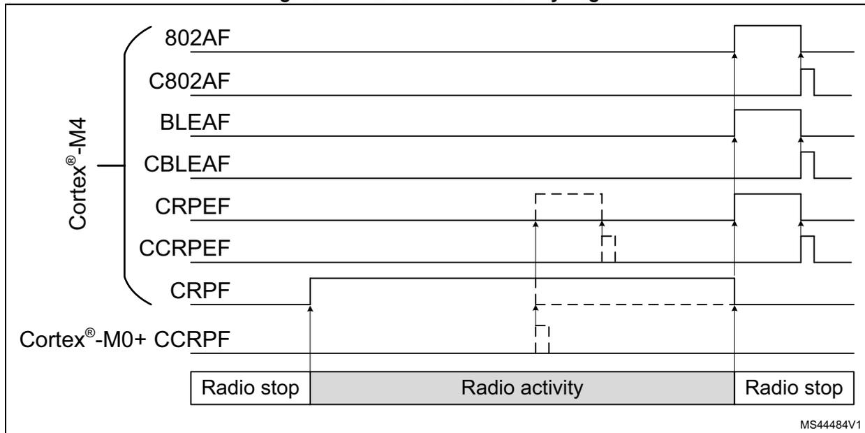
When enabled, the radio activity end interrupt flag 802AF indicates the end of an IEEE802.15.4 radio activity period, and is generated when the radio enters Cstop mode.
When enabled, the radio activity end interrupt flag BLEAF indicates the end of a BLE radio activity period, and is generated when the radio enters Cstop mode.
The critical radio phase flag indicates the critical real time phase of the radio, where access to the flash memory must not be blocked by erase or program operations (all erase and program operations are suspended by the CPU2 in the flash memory interface). The end of the critical radio phase may be triggered by the CPU2 clearing the critical radio phase flag CRPF, and is eventually cleared at the end of the IEEE802.15.4 or BLE radio activity.
When enabled, the critical radio phase end interrupt flag CRPEF indicates the end of a radio critical phase, and is generated when the radio critical phase ends.
5.6 PWR registers
The peripheral registers can be accessed by half-words (16-bit) or words (32-bit).
5.6.1 PWR control register 1 (PWR_CR1)
Address offset: 0x000
Reset value: 0x0000 0200. This register is reset after wake-up from Standby mode, except for bits [2:0].
| 31 | 30 | 29 | 28 | 27 | 26 | 25 | 24 | 23 | 22 | 21 | 20 | 19 | 18 | 17 | 16 |
|---|---|---|---|---|---|---|---|---|---|---|---|---|---|---|---|
| Res. | Res. | Res. | Res. | Res. | Res. | Res. | Res. | Res. | Res. | Res. | Res. | Res. | Res. | Res. | Res. |
| 15 | 14 | 13 | 12 | 11 | 10 | 9 | 8 | 7 | 6 | 5 | 4 | 3 | 2 | 1 | 0 |
| Res. | LPR | Res. | Res. | Res. | VOS[1:0] | DBP | Res. | Res. | FPDS | FPDR | Res. | LPMS[2:0] | |||
| rw | rw | rw | rw | rw | rw | rw | rw | rw | |||||||
Bits 31:15 Reserved, must be kept at reset value.
Bit 14 LPR : Low-power run
When this bit is set, the regulator is switched from main mode (MR) to low-power mode (LPR).
Note: Stop2 mode cannot be entered when LPR bit is set. Stop1 is entered instead.
Bits 13:11 Reserved, must be kept at reset value.
Bits 10:9 VOS : Voltage scaling range selection
00: Cannot be written (forbidden by hardware)
01: Range 1
10: Range 2
11: Cannot be written (forbidden by hardware)
Bit 8 DBP : Disable backup domain write protection
In reset state, the RTC and backup registers are protected against parasitic write access. This bit must be set to enable write access to these registers.
0: Access to RTC and Backup registers disabled
1: Access to RTC and Backup registers enabled
Bits 7:6 Reserved, must be kept at reset value.
Bit 5 FPDS : Flash memory power down mode during LPSleep for CPU1
This bit selects whether the flash memory is in power down mode or idle mode when both CPUs are in Sleep mode. flash memory is set in power down mode only when the system is in LPSleep mode and the PWR_C2CR1.FPDS bit from CPU2 also allows this.
0: Flash memory in Idle mode when system is in LPSleep mode
1: Flash memory in power down mode when system is in LPSleep mode
Bit 4 FPDR : Flash memory power down mode during LPRun for CPU1
This bit can only be written to 1 after unlocking this register bit, by first writing (code 0xC1B0) into this register (when writing the code, the register bits are not updated). Selects whether the flash memory is in power down mode or idle mode when in LPRun mode. (flash memory can only be in power down mode when code is executed from SRAM). Flash memory is set in power down mode only when the system is in LPRun mode, and the PWR_C2CR1.FPDR bit from CPU2 too allows so.
0: Flash memory in Idle mode when system is in LPRun mode
1: Flash memory in power down mode when system is in LPRun mode
Bit 3 Reserved, must be kept at reset value.
Bits 2:0 LPMS[2:0] : Low-power mode selection for CPU1
These bits are not reset when exiting Standby mode.
These bits select the low-power mode allowed when CPU1 enters the deepsleep mode. The entered system low-power mode depends also upon the PWR_C2CR1.LPMS allowed low-power mode from CPU2.
000: Stop0 mode
001: Stop1 mode
010: Stop2 mode
011: Standby mode
1xx: Shutdown mode
Note: If LPR bit is set, Stop2 mode cannot be selected and Stop1 mode must be entered instead of Stop2.
In Standby mode, SRAM2 can be preserved or not, depending on RRS bit configuration in PWR_CR3.
5.6.2 PWR control register 2 (PWR_CR2)
Address offset: 0x004
Reset value: 0x0000 0000. This register is reset when exiting Standby mode.
| 31 | 30 | 29 | 28 | 27 | 26 | 25 | 24 | 23 | 22 | 21 | 20 | 19 | 18 | 17 | 16 |
|---|---|---|---|---|---|---|---|---|---|---|---|---|---|---|---|
| Res. | Res. | Res. | Res. | Res. | Res. | Res. | Res. | Res. | Res. | Res. | Res. | Res. | Res. | Res. | Res. |
| 15 | 14 | 13 | 12 | 11 | 10 | 9 | 8 | 7 | 6 | 5 | 4 | 3 | 2 | 1 | 0 |
| Res. | Res. | Res. | Res. | Res. | USV | Res. | Res. | Res. | PVME3 | Res. | PVME1 | PLS[2:0] | PVDE | ||
| rw | rw | rw | rw | rw | rw | rw | |||||||||
Bits 31:11 Reserved, must be kept at reset value.
Bit 10 USV : V DDUSB USB supply valid
This bit is used to validate the V DDUSB supply for electrical and logical isolation purposes.
Setting this bit is mandatory to use the USB FS peripheral. If V DDUSB is not always present in the application, the PVM can be used to determine whether this supply is available or not.
0: V DDUSB is not present. Logical and electrical isolation is applied to ignore this supply.
1: V DDUSB is valid.
Bits 9:7 Reserved, must be kept at reset value.
Bit 6 PVME3 : Peripheral voltage monitoring 3 enable: V DDA vs. 1.62 V
0: PVM3 (V DDA monitoring vs. 1.62 V threshold) disabled
1: PVM3 (V DDA monitoring vs. 1.62 V threshold) enabled
Bit 5 Reserved, must be kept at reset value.
Bit 4 PVME1 : Peripheral voltage monitoring 1 enable: \( V_{DDUSB} \) vs. 1.2 V
0: PVM1 ( \( V_{DDUSB} \) monitoring vs. 1.2 V threshold) disabled.
1: PVM1 ( \( V_{DDUSB} \) monitoring vs. 1.2 V threshold) enabled.
Bits 3:1 PLS[2:0] : Programmable voltage detector level selection.
These bits select the voltage threshold detected by the Programmable voltage detector:
000: \( V_{PVD0} \sim 2.0 \) V
001: \( V_{PVD1} \sim 2.2 \) V
010: \( V_{PVD2} \sim 2.4 \) V
011: \( V_{PVD3} \sim 2.5 \) V
100: \( V_{PVD4} \sim 2.6 \) V
101: \( V_{PVD5} \sim 2.8 \) V
110: \( V_{PVD6} \sim 2.9 \) V
111: External input analog voltage \( PVD\_IN \) (compared internally to \( V_{REFINT} \) ). The I/O used as \( PVD\_IN \) input must be configured in analog mode in the GPIO register.
Note: These bits are write-protected when the bit PVDL (PVD lock) is set in the SYSCFG_CBR register, they are reset only by a system reset.
Bit 0 PVDE : Programmable voltage detector enable
0: Programmable voltage detector disabled
1: Programmable voltage detector enabled
Note: This bit is write-protected when bit PVDL (PVD lock) is set in the SYSCFG_CBR register. This bit is reset only by a system reset.
5.6.3 PWR control register 3 (PWR_CR3)
Address offset: 0x008
Reset value: 0x0000 8000. This register is not reset when exiting Standby modes.
Access: Additional APB cycles are needed to access this register vs. those needed for a standard APB access (three for a write and two for a read).
| 31 | 30 | 29 | 28 | 27 | 26 | 25 | 24 | 23 | 22 | 21 | 20 | 19 | 18 | 17 | 16 |
|---|---|---|---|---|---|---|---|---|---|---|---|---|---|---|---|
| Res. | Res. | Res. | Res. | Res. | Res. | Res. | Res. | Res. | Res. | Res. | Res. | Res. | Res. | Res. | Res. |
| 15 | 14 | 13 | 12 | 11 | 10 | 9 | 8 | 7 | 6 | 5 | 4 | 3 | 2 | 1 | 0 |
| EIWUL | EC2H | E802A | EBLEA | ECRPE | APC | RRS | EBORH SMPSFB | Res. | Res. | Res. | EWUP5 | EWUP4 | EWUP3 | EWUP2 | EWUP1 |
| rw | rw | rw | rw | rw | rw | rw | rw | rw | rw | rw | rw | rw |
Bits 31:16 Reserved, must be kept at reset value.
Bit 15 EIWUL : Enable internal wake-up line for CPU1
0: Internal wake-up line interrupt to CPU1 disabled
1: Internal wake-up line interrupt to CPU1 enabled
Bit 14 EC2H : Enable CPU2 Hold interrupt for CPU1
Enable CPU2 kept in hold, due to C2BOOT, interrupt to CPU1.
0: Interrupt to CPU1 disabled
1: interrupt to CPU1 enabled
Bit 13 E802A : Enable 802.15.4 end of activity interrupt for CPU1
0: Interrupt to CPU1 disabled
1: interrupt to CPU1 enabled
Bit 12 EBLEA : Enable BLE end of activity interrupt for CPU1
0: Interrupt to CPU1 disabled
1: interrupt to CPU1 enabled
Bit 11 ECRPE : Enable critical radio phase end of activity interrupt for CPU1
0: Interrupt to CPU1 disabled
1: interrupt to CPU1 enabled
Bit 10 APC : Apply pull-up and pull-down configuration from CPU1
When this bit for CPU1 or the PWR_C2CR3.APC bit for CPU2 is set, the I/O pull-up and pull-down configurations defined in the PWR_PUCRx and PWR_PDCRx registers are applied. When both bits are cleared, the PWR_PUCRx and PWR_PDCRx registers are not applied to the I/Os.
Bit 9 RRS : SRAM2a retention in Standby mode
0: SRAM2a powered off in Standby mode (content is lost).
1: SRAM2a powered by the low-power regulator in Standby mode (content is kept).
Bit 8 EBORHSMPSFB : Enable BORH and SMPS step-down converter forced in Bypass interrupts for CPU1
0: Interrupts BORHF and SMPSFBF to CPU1 disabled
1: interrupts BORHF and SMPSFBF to CPU1 enabled
Bits 7:5 Reserved, must be kept at reset value.
Bit 4 EWUP5 : Enable wake-up pin WKUP5 for CPU1 (available on STM32WB55xx only)
When this bit is set, the external wake-up pin WKUP5 is enabled and triggers an interrupt and wake-up from Stop, Standby or Shutdown event when a rising or a falling edge occurs to CPU1. The active edge is configured via the WP5 bit in the PWR control register 4 (PWR_CR4) . Note that this bit is reserved in STM32WB35xx devices.
Bit 3 EWUP4 : Enable wake-up pin WKUP4 for CPU1
When this bit is set, the external wake-up pin WKUP4 is enabled and triggers an interrupt and wake-up from Stop, Standby or Shutdown event when a rising or a falling edge occurs to CPU1. The active edge is configured via the WP4 bit in the PWR control register 4 (PWR_CR4) .
Bit 2 EWUP3 : Enable wake-up pin WKUP3 for CPU1 (available on STM32WB55xx only)
When this bit is set, the external wake-up pin WKUP3 is enabled and triggers an interrupt and wake-up from Stop, Standby or Shutdown event when a rising or a falling edge occurs to CPU1. The active edge is configured via the WP3 bit in the PWR control register 4 (PWR_CR4) . Note that this bit is reserved in STM32WB35xx devices.
Bit 1 EWUP2 : Enable wake-up pin WKUP2 for CPU1 (available on STM32WB55xx only)
When this bit is set, the external wake-up pin WKUP2 is enabled and triggers an interrupt and wake-up from Stop, Standby or Shutdown event when a rising or a falling edge occurs to CPU1. The active edge is configured via the WP2 bit in the PWR control register 4 (PWR_CR4) . Note that this bit is reserved in STM32WB35xx devices.
Bit 0 EWUP1 : Enable wake-up pin WKUP1 for CPU1
When this bit is set, the external wake-up pin WKUP1 is enabled and triggers an interrupt and wake-up from Stop, Standby or Shutdown event when a rising or a falling edge occurs to CPU1. The active edge is configured via the WP1 bit in the PWR control register 4 (PWR_CR4) .
5.6.4 PWR control register 4 (PWR_CR4)
Address offset: 0x00C
Reset value: 0x0000 0000. This register is not reset when exiting Standby modes.
Access: Additional APB cycles are needed to access this register vs. those needed for a standard APB access (three for a write and two for a read).
| 31 | 30 | 29 | 28 | 27 | 26 | 25 | 24 | 23 | 22 | 21 | 20 | 19 | 18 | 17 | 16 |
|---|---|---|---|---|---|---|---|---|---|---|---|---|---|---|---|
| Res. | Res. | Res. | Res. | Res. | Res. | Res. | Res. | Res. | Res. | Res. | Res. | Res. | Res. | Res. | Res. |
| 15 | 14 | 13 | 12 | 11 | 10 | 9 | 8 | 7 | 6 | 5 | 4 | 3 | 2 | 1 | 0 |
| C2BOOT | Res. | Res. | Res. | Res. | Res. | VBRS | VBE | Res. | Res. | Res. | WP5 | WP4 | WP3 | WP2 | WP1 |
| rw | rw | rw | rw | rw | rw | rw | rw | ||||||||
Bits 31:16 Reserved, must be kept at reset value.
Bit 15 C2BOOT : Boot CPU2 after reset or wake-up from Stop or Standby modes.
- 0: CPU2 does not boot after reset or wake-up from Stop or Standby modes.
- 1: CPU2 boots after wake-up from Stop or Standby modes.
Bits 14:10 Reserved, must be kept at reset value.
Bit 9 VBRS : \( V_{BAT} \) battery charging resistor selection
- 0: Charge \( V_{BAT} \) through a 5 k \( \Omega \) resistor
- 1: Charge \( V_{BAT} \) through a 1.5 k \( \Omega \) resistor
Bit 8 VBE : \( V_{BAT} \) battery charging enable
- 0: \( V_{BAT} \) battery charging disabled
- 1: \( V_{BAT} \) battery charging enabled
Bits 7:5 Reserved, must be kept at reset value.
Bit 4 WP5 : Wakeup pin WKUP5 polarity (available on STM32WB55xx only)
This bit defines the polarity used for an event detection on external wake-up pin, WKUP5
- 0: Detection on high level (rising edge)
- 1: Detection on low level (falling edge)
Note that this bit is reserved in STM32WB35xx devices.
Bit 3 WP4 : Wakeup pin WKUP4 polarity
This bit defines the polarity used for an event detection on external wake-up pin, WKUP4
- 0: Detection on high level (rising edge)
- 1: Detection on low level (falling edge)
Bit 2 WP3 : Wakeup pin WKUP3 polarity (available on STM32WB55xx only)
This bit defines the polarity used for an event detection on external wake-up pin, WKUP3
- 0: Detection on high level (rising edge)
- 1: Detection on low level (falling edge)
Note that this bit is reserved in STM32WB35xx devices.
Bit 1 WP2 : Wakeup pin WKUP2 polarity (available on STM32WB55xx only)
This bit defines the polarity used for an event detection on external wake-up pin, WKUP2
- 0: Detection on high level (rising edge)
- 1: Detection on low level (falling edge)
Note that this bit is reserved in STM32WB35xx devices.
Bit 0 WP1 : Wakeup pin WKUP1 polarity
This bit defines the polarity used for an event detection on external wake-up pin, WKUP1
0: Detection on high level (rising edge)
1: Detection on low level (falling edge)
5.6.5 PWR status register 1 (PWR_SR1)
Address offset: 0x010
Reset value: 0x0000 0000. This register is not reset when exiting Standby modes.
Access: Two additional APB cycles are needed to read this register vs. a standard APB read.
| 31 | 30 | 29 | 28 | 27 | 26 | 25 | 24 | 23 | 22 | 21 | 20 | 19 | 18 | 17 | 16 |
|---|---|---|---|---|---|---|---|---|---|---|---|---|---|---|---|
| Res. | Res. | Res. | Res. | Res. | Res. | Res. | Res. | Res. | Res. | Res. | Res. | Res. | Res. | Res. | Res. |
| 15 | 14 | 13 | 12 | 11 | 10 | 9 | 8 | 7 | 6 | 5 | 4 | 3 | 2 | 1 | 0 |
| WUFI | C2HF | 802AF | BLE AF | CRPEF | 802 WUF | BLE WUF | BORHF | SMPS FBF | Res. | Res. | WUF5 | WUF4 | WUF3 | WUF2 | WUF1 |
| r | r | r | r | r | r | r | r | r | r | r | r | r | r | ||
Bits 31:16 Reserved, must be kept at reset value.
Bit 15 WUFI : Internal wake-up interrupt flag
This bit is set when a wake-up is detected on the internal wake-up line. It is cleared when all internal wake-up sources are cleared.
Bit 14 C2HF : CPU2 Hold interrupt flag
This bit is set when a CPU2 wake-up is detected when C2BOOT = 0. It is cleared by PWR_SCR.CC2HF.
Bit 13 802AF : 802.15.4 end of activity interrupt flag
This bit is set when a 802.15.4 activity ends. It is cleared by PWR_SCR.C802AF.
Bit 12 BLEAF : BLE end of activity interrupt flag
This bit is set when a BLE activity ends. It is cleared by PWR_SCR.CBLEAF.
Bit 11 CRPEF : Enable critical radio phase end of activity interrupt flag
This bit is set when Radio phase activity ends. It is cleared by PWR_SCR.CCRPEF.
Bit 10 802WUF : 802.15.4 wake-up interrupt flag
This bit is set when a wake-up is detected on the 802.15.4 line. It is cleared by PWR_SCR.C802WUF.
Bit 9 BLEWUF : BLE wake-up interrupt flag
This bit is set when a wake-up is detected on the BLE line. It is cleared by PWR_SCR.CBLEWUF.
Bit 8 BORHF : BORH interrupt flag
This bit is set when the V DD rises above the BORH threshold. It is cleared by PWR_SCR.CBORHF.
Bit 7 SMPSFBF : SMPS step-down converter forced in Bypass interrupt flag
This bit is set when the SMPS step-down converter is enabled in SMPS mode and forced in Bypass mode due to the BORH threshold. BORH configuration by BORHC bit in PWR control register 5 (PWR_CR5) must select BORH force SMPS step-down converter in Bypass mode.
This bit is cleared by PWR_SCR.CSMPSFBF.
Bits 6:5 Reserved, must be kept at reset value.
Bit 4 WUF5 : Wakeup flag 5 (available on STM32WB55xx only)
This bit is set when a wake-up event is detected on wake-up pin, WKUP5. It is cleared by writing '1' in the CWUF5 bit of the PWR_SCR register. Note that this bit is reserved in STM32WB35xx devices.
Bit 3 WUF4 : Wakeup flag 4
This bit is set when a wake-up event is detected on wake-up pin, WKUP4. It is cleared by writing '1' in the CWUF4 bit of the PWR status clear register (PWR_SCR) .
Bit 2 WUF3 : Wakeup flag 3 (available on STM32WB55xx only)
This bit is set when a wake-up event is detected on wake-up pin, WKUP3. It is cleared by writing '1' in the CWUF3 bit of the PWR status clear register (PWR_SCR) . Note that this bit is reserved in STM32WB35xx devices.
Bit 1 WUF2 : Wakeup flag 2 (available on STM32WB55xx only)
This bit is set when a wake-up event is detected on wake-up pin, WKUP2. It is cleared by writing '1' in the CWUF2 bit of the PWR status clear register (PWR_SCR) . Note that this bit is reserved in STM32WB35xx devices.
Bit 0 WUF1 : Wakeup flag 1
This bit is set when a wake-up event is detected on wake-up pin, WKUP1. It is cleared by writing '1' in the CWUF1 bit of the PWR status clear register (PWR_SCR) .
5.6.6 PWR status register 2 (PWR_SR2)
Address offset: 0x014
Reset value: 0x0000 0002. This register is partially reset when exiting Standby/Shutdown modes.
| 31 | 30 | 29 | 28 | 27 | 26 | 25 | 24 | 23 | 22 | 21 | 20 | 19 | 18 | 17 | 16 |
|---|---|---|---|---|---|---|---|---|---|---|---|---|---|---|---|
| Res. | Res. | Res. | Res. | Res. | Res. | Res. | Res. | Res. | Res. | Res. | Res. | Res. | Res. | Res. | Res. |
| 15 | 14 | 13 | 12 | 11 | 10 | 9 | 8 | 7 | 6 | 5 | 4 | 3 | 2 | 1 | 0 |
| Res. | PVM03 | Res. | PVM01 | PVDO | VOSF | REGLPF | REGLPS | Res. | Res. | Res. | Res. | Res. | Res. | SMPSF | SMPSBF |
| r | r | r | r | r | r | r | r |
Bits 31:15 Reserved, must be kept at reset value.
Bit 14 PVM03 : Peripheral voltage monitoring output: V DDA vs. 1.62 V
0: V DDA voltage is above PVM3 threshold (~ 1.62 V)
1: V DDA voltage is below PVM3 threshold (~ 1.62 V)
Note: PVM03 is cleared when PVM3 is disabled (PVME3 = 0). After enabling PVM3, the PVM3 output is valid after the PVM3 wake-up time.
Bit 13 Reserved, must be kept at reset value.
Bit 12 PVMO1 : Peripheral voltage monitoring output: V DDUSB vs. 1.2 V
0: V DDUSB voltage is above PWM1 threshold (~ 1.2 V)
1: V DDUSB voltage is below PWM1 threshold (~ 1.2 V)
Note: PVMO1 is cleared when PWM1 is disabled (PVME1 = 0). After enabling PWM1, the PWM1 output is valid after the PWM1 wake-up time.
Bit 11 PVDO : Programmable voltage detector output
0: V DD or voltage level on PVD_IN is above the selected PVD threshold
1: V DD or voltage level on PVD_IN is below the selected PVD threshold
Bit 10 VOSF : Voltage scaling flag
A delay is required for the internal regulator to be ready after the voltage scaling has been changed. VOSF indicates that the regulator reached the voltage level defined with VOS bits of the PWR control register 1 (PWR_CR1) .
0: The regulator is ready in the selected voltage range
1: The regulator output voltage is changing to the required voltage level
Bit 9 REGLPF : Low-power regulator flag
This bit is set by hardware when the MCU is in Low-power run mode. When the MCU exits from the Low-power run mode, this bit remains at 1 until the regulator is ready in main mode. A polling on this bit must be done before increasing the product frequency.
This bit is cleared by hardware when the regulator is ready.
0: The regulator is ready in main mode (MR)
1: The regulator is in low-power mode (LPR)
Bit 8 REGLPS : Low-power regulator started
This bit provides the information whether the low-power regulator is ready after a power-on reset or a Standby/Shutdown. If the Standby mode is entered while REGLPS bit is still cleared, the wake-up from Standby mode time may be increased.
0: The low-power regulator is not ready
1: The low-power regulator is ready
Bits 7:2 Reserved, must be kept at reset value.
Bit 1 SMPSF : SMPS step-down converter SMPS mode flag
This bit indicates that the SMPS step-down converter is in SMPS mode.
0: The SMPS step-down converter is not ready
1: The SMPS step-down converter is ready
Bit 0 SMPSBF : SMPS step-down converter Bypass mode flag
This bit indicates that the SMPS step-down converter is in Bypass mode.
0: The SMPS step-down converter is not in Bypass mode (either in Open or SMPS mode)
1: The SMPS step-down converter is in Bypass mode
5.6.7 PWR status clear register (PWR_SCR)
Address offset: 0x018
Reset value: 0x0000 0000
Access: Three additional APB cycles are needed to write this register vs. a standard APB write.
| 31 | 30 | 29 | 28 | 27 | 26 | 25 | 24 | 23 | 22 | 21 | 20 | 19 | 18 | 17 | 16 |
|---|---|---|---|---|---|---|---|---|---|---|---|---|---|---|---|
| Res. | Res. | Res. | Res. | Res. | Res. | Res. | Res. | Res. | Res. | Res. | Res. | Res. | Res. | Res. | Res. |
| 15 | 14 | 13 | 12 | 11 | 10 | 9 | 8 | 7 | 6 | 5 | 4 | 3 | 2 | 1 | 0 |
| Res. | CC2HF | C802 AF | CFBLE AF | CCRP EF | C802 WUF | CBLE WUF | CBORH F | CSMPS FBF | Res. | Res. | CWUF5 | CWUF4 | CWUF3 | CWUF2 | CWUF1 |
| w | w | w | w | w | w | w | w | w | w | w | w | w |
Bits 31:15 Reserved, must be kept at reset value.
Bit 14 CC2HF : Clear CPU2 Hold interrupt flag
Setting this bit clears the C2HF flag in the PWR_SR1. This bit is always read 0.
Bit 13 C802AF : Clear 802.15.4 end of activity interrupt flag
Setting this bit clears the 802AF flag in the PWR_SR1. This bit is always read 0.
Bit 12 CBLEAF : Clear BLE end of activity interrupt flag
Setting this bit clears the BLEAF flag in the PWR_SR1. This bit is always read 0.
Bit 11 CCRPEF : Clear critical radio phase end of activity interrupt flag
Setting this bit clears the CRPEF flag in the PWR_SR1. This bit is always read 0.
Bit 10 C802WUF Clear 802.15.4 wake-up interrupt flag
Setting this bit clears the 802WUF flag in the PWR_SR1. This bit is always read 0.
Bit 9 CBLEWUF Clear BLE wake-up interrupt flag
Setting this bit clears the BLEWUF flag in the PWR_SR1. This bit is always read 0.
Bit 8 CBORHF : Clear BORH interrupt flag
Setting this bit clears the SBORHF flag in the PWR_SR1. This bit is always read 0.
Bit 7 CSMPSFBF : Clear SMPS step-down converter forced in Bypass interrupt flag
Setting this bit clears the SMPSFBF flag in the PWR_SR1. This bit is always read 0.
Bits 6:5 Reserved, must be kept at reset value.
Bit 4 CWUF5 : Clear wake-up flag 5 (available on STM32WB55xx only)
Setting this bit clears the WUF5 flag in the PWR_SR1 register.
Note that this bit is reserved in STM32WB35xx devices.
Bit 3 CWUF4 : Clear wake-up flag 4
Setting this bit clears the WUF4 flag in the PWR_SR1 register.
Bit 2 CWUF3 : Clear wake-up flag 3 (available on STM32WB55xx only)
Setting this bit clears the WUF3 flag in the PWR_SR1 register.
Note that this bit is reserved in STM32WB35xx devices.
Bit 1 CWUF2 : Clear wake-up flag 2 (available on STM32WB55xx only)
Setting this bit clears the WUF2 flag in the PWR_SR1 register.
Note that this bit is reserved in STM32WB35xx devices.
Bit 0 CWUF1 : Clear wake-up flag 1
Setting this bit clears the WUF1 flag in the PWR_SR1 register.
5.6.8 PWR control register 5 (PWR_CR5)
Address offset: 0x01C
Reset value: 0x0000 427X, where X is factory-programmed. This register is not reset when exiting Standby modes.
Access: Three additional APB cycles are needed to write this register vs. a standard APB write.
| 31 | 30 | 29 | 28 | 27 | 26 | 25 | 24 | 23 | 22 | 21 | 20 | 19 | 18 | 17 | 16 |
|---|---|---|---|---|---|---|---|---|---|---|---|---|---|---|---|
| Res. | Res. | Res. | Res. | Res. | Res. | Res. | Res. | Res. | Res. | Res. | Res. | Res. | Res. | Res. | Res. |
| 15 | 14 | 13 | 12 | 11 | 10 | 9 | 8 | 7 | 6 | 5 | 4 | 3 | 2 | 1 | 0 |
| SMPSEN | Res. | Res. | Res. | Res. | Res. | Res. | BORHC | Res. | .SMPSSC[2:0] | SMPSVOS[3:0] | |||||
| rw | rw | rw | rw | rw | rw | rw | rw | rw | |||||||
Bits 31:16 Reserved, must be kept at reset value.
Bit 15 SMPSEN : Enable SMPS step-down converter SMPS mode enabled.
This bit is reset to 0 when SMPS step-down converter switching on the fly is enabled and the \( V_{DD} \) level drops below the BORH threshold.
0: SMPS Step down converter SMPS mode disabled.
1: SMPS Step down converter SMPS mode enabled.
Note: The noise performance of analog signals may be impacted by the integrated SMPS switching. To prevent this the SMPS may be switched off on the fly when measuring analog signals.
Bits 14:9 Reserved, must be kept at reset value.
Bit 8 BORHC : BORH configuration selection
0: BORH generates a system reset.
1: BORH forces SMPS step-down converter Bypass mode (BORL still generates a system reset).
Bit 7 Reserved, must be kept at reset value.
Bits 6:4 SMPSSC : SMPS step-down converter supply startup current selection
Startup current is limited to maximum 80 mA + SMPSSC x 20 mA.
Bit 3:0 SMPSVOS : SMPS step-down converter voltage output scaling
These bits are initialized after Option byte loading with factory trimmed value to reach 1.5 V, and can subsequently be overwritten by firmware.
SMPS step down output voltage step size is 50 mV.
If factory trimmed value - 0x8 gives 1.50 V on \( V_{FBSMPS} \) , to get 1.40 V 0x2 must be subtracted from this value.
- – 0x0 = minimum voltage level
- – 0xF = maximum voltage level
The factory trimmed value can be obtained from address 0x1FFF 7558 bits [11:8].
5.6.9 PWR Port A pull-up control register (PWR_PUCRA)
Address offset: 0x020
Reset value: 0x0000 0000. This register is not reset when exiting Standby modes.
Access: Additional APB cycles are needed to access this register vs. those needed for a standard APB access (three for a write and two for a read).
| 31 | 30 | 29 | 28 | 27 | 26 | 25 | 24 | 23 | 22 | 21 | 20 | 19 | 18 | 17 | 16 |
|---|---|---|---|---|---|---|---|---|---|---|---|---|---|---|---|
| Res. | Res. | Res. | Res. | Res. | Res. | Res. | Res. | Res. | Res. | Res. | Res. | Res. | Res. | Res. | Res. |
| 15 | 14 | 13 | 12 | 11 | 10 | 9 | 8 | 7 | 6 | 5 | 4 | 3 | 2 | 1 | 0 |
| PU15 | PU14 | PU13 | PU12 | PU11 | PU10 | PU9 | PU8 | PU7 | PU6 | PU5 | PU4 | PU3 | PU2 | PU1 | PU0 |
| rw | rw | rw | rw | rw | rw | rw | rw | rw | rw | rw | rw | rw | rw | rw | rw |
Bits 31:16 Reserved, must be kept at reset value.
Bits 15:0 PUy : Port A pull-up bit y (y=0...15)
When set, this bit activates the pull-up on Px[y] when one of the APC bits is set in PWR control register 3 (PWR_CR3) and in PWR CPU2 control register 3 (PWR_C2CR3) . The pull-up is not activated if the corresponding PDy bit is also set.
5.6.10 PWR Port A pull-down control register (PWR_PDCRA)
Address offset: 0x024
Reset value: 0x0000 0000. This register is not reset when exiting Standby modes.
Access: Additional APB cycles are needed to access this register vs. those needed for a standard APB access (three for a write and two for a read).
| 31 | 30 | 29 | 28 | 27 | 26 | 25 | 24 | 23 | 22 | 21 | 20 | 19 | 18 | 17 | 16 |
|---|---|---|---|---|---|---|---|---|---|---|---|---|---|---|---|
| Res. | Res. | Res. | Res. | Res. | Res. | Res. | Res. | Res. | Res. | Res. | Res. | Res. | Res. | Res. | Res. |
| 15 | 14 | 13 | 12 | 11 | 10 | 9 | 8 | 7 | 6 | 5 | 4 | 3 | 2 | 1 | 0 |
| PD15 | PD14 | PD13 | PD12 | PD11 | PD10 | PD9 | PD8 | PD7 | PD6 | PD5 | PD4 | PD3 | PD2 | PD1 | PD0 |
| rw | rw | rw | rw | rw | rw | rw | rw | rw | rw | rw | rw | rw | rw | rw | rw |
Bits 31:16 Reserved, must be kept at reset value.
Bits 15:0 PDy : Port A pull-down bit y (y=0...15)
When set, this bit activates the pull-down on PA[y] when one of the APC bits is set in PWR control register 3 (PWR_CR3) and in PWR CPU2 control register 3 (PWR_C2CR3) .
5.6.11 PWR Port B pull-up control register (PWR_PUCRB)
Address offset: 0x028
Reset value: 0x0000 0000. This register is not reset when exiting Standby modes.
Access: Additional APB cycles are needed to access this register vs. those needed for a standard APB access (three for a write and two for a read).
| 31 | 30 | 29 | 28 | 27 | 26 | 25 | 24 | 23 | 22 | 21 | 20 | 19 | 18 | 17 | 16 |
|---|---|---|---|---|---|---|---|---|---|---|---|---|---|---|---|
| Res. | Res. | Res. | Res. | Res. | Res. | Res. | Res. | Res. | Res. | Res. | Res. | Res. | Res. | Res. | Res. |
| 15 | 14 | 13 | 12 | 11 | 10 | 9 | 8 | 7 | 6 | 5 | 4 | 3 | 2 | 1 | 0 |
| PU15 | PU14 | PU13 | PU12 | PU11 | PU10 | PU9 | PU8 | PU7 | PU6 | PU5 | PU4 | PU3 | PU2 | PU1 | PU0 |
| rw | rw | rw | rw | rw | rw | rw | rw | rw | rw | rw | rw | rw | rw | rw | rw |
Bits 31:16 Reserved, must be kept at reset value.
Bits 15:0 PUy : Port B pull-up bit y (y=0...15)
When set, this bit activates the pull-up on Px[y] when one of the APC bits is set in PWR control register 3 (PWR_CR3) and in PWR CPU2 control register 3 (PWR_C2CR3) . The pull-up is not activated if the corresponding PDy bit is also set. Note that bits 15:10 are reserved in STM32WB35xx devices.
5.6.12 PWR Port B pull-down control register (PWR_PDCRB)
Address offset: 0x02C
Reset value: 0x0000 0000. This register is not reset when exiting Standby modes.
Access: Additional APB cycles are needed to access this register vs. those needed for a standard APB access (three for a write and two for a read).
| 31 | 30 | 29 | 28 | 27 | 26 | 25 | 24 | 23 | 22 | 21 | 20 | 19 | 18 | 17 | 16 |
|---|---|---|---|---|---|---|---|---|---|---|---|---|---|---|---|
| Res. | Res. | Res. | Res. | Res. | Res. | Res. | Res. | Res. | Res. | Res. | Res. | Res. | Res. | Res. | Res. |
| 15 | 14 | 13 | 12 | 11 | 10 | 9 | 8 | 7 | 6 | 5 | 4 | 3 | 2 | 1 | 0 |
| PD15 | PD14 | PD13 | PD12 | PD11 | PD10 | PD9 | PD8 | PD7 | PD6 | PD5 | PD4 | PD3 | PD2 | PD1 | PD0 |
| rw | rw | rw | rw | rw | rw | rw | rw | rw | rw | rw | rw | rw | rw | rw | rw |
Bits 31:16 Reserved, must be kept at reset value.
Bits 15:0 PDy : Port B pull-down bit y (y=0...15)
When set, this bit activates the pull-down on PB[y] when one of the APC bits is set in PWR control register 3 (PWR_CR3) and in PWR CPU2 control register 3 (PWR_C2CR3) . Note that bits 15:10 are reserved in STM32WB35xx devices.
5.6.13 PWR Port C pull-up control register (PWR_PUCRC)
Address offset: 0x030
Reset value: 0x0000 0000. This register is not reset when exiting Standby modes.
Access: Additional APB cycles are needed to access this register vs. those needed for a standard APB access (three for a write and two for a read).
| 31 | 30 | 29 | 28 | 27 | 26 | 25 | 24 | 23 | 22 | 21 | 20 | 19 | 18 | 17 | 16 |
|---|---|---|---|---|---|---|---|---|---|---|---|---|---|---|---|
| Res. | Res. | Res. | Res. | Res. | Res. | Res. | Res. | Res. | Res. | Res. | Res. | Res. | Res. | Res. | Res. |
| 15 | 14 | 13 | 12 | 11 | 10 | 9 | 8 | 7 | 6 | 5 | 4 | 3 | 2 | 1 | 0 |
| PU15 | PU14 | PU13 | PU12 | PU11 | PU10 | PU9 | PU8 | PU7 | PU6 | PU5 | PU4 | PU3 | PU2 | PU1 | PU0 |
| rw | rw | rw | rw | rw | rw | rw | rw | rw | rw | rw | rw | rw | rw | rw | rw |
Bits 31:16 Reserved, must be kept at reset value.
Bits 15:0 PUy : Port C pull-up bit y (y=0...15)
When set, this bit activates the pull-up on Px[y] when one of the APC bits is set in PWR control register 3 (PWR_CR3) and in PWR CPU2 control register 3 (PWR_C2CR3) . The pull-up is not activated if the corresponding PDy bit is also set. Note that bits 13:0 are reserved in STM32WB35xx devices.
5.6.14 PWR Port C pull-down control register (PWR_PDCRC)
Address offset: 0x034
Reset value: 0x0000 0000. This register is not reset when exiting Standby modes.
Access: Additional APB cycles are needed to access this register vs. those needed for a standard APB access (three for a write and two for a read).
| 31 | 30 | 29 | 28 | 27 | 26 | 25 | 24 | 23 | 22 | 21 | 20 | 19 | 18 | 17 | 16 |
|---|---|---|---|---|---|---|---|---|---|---|---|---|---|---|---|
| Res. | Res. | Res. | Res. | Res. | Res. | Res. | Res. | Res. | Res. | Res. | Res. | Res. | Res. | Res. | Res. |
| 15 | 14 | 13 | 12 | 11 | 10 | 9 | 8 | 7 | 6 | 5 | 4 | 3 | 2 | 1 | 0 |
| PD15 | PD14 | PD13 | PD12 | PD11 | PD10 | PD9 | PD8 | PD7 | PD6 | PD5 | PD4 | PD3 | PD2 | PD1 | PD0 |
| rw | rw | rw | rw | rw | rw | rw | rw | rw | rw | rw | rw | rw | rw | rw | rw |
Bits 31:16 Reserved, must be kept at reset value.
Bits 15:0 PDy : Port C pull-down bit y (y=0...15)
When set, this bit activates the pull-down on PC[y] when one of the APC bits is set in PWR control register 3 (PWR_CR3) and in PWR CPU2 control register 3 (PWR_C2CR3) . Note that bits 13:0 are reserved in STM32WB35xx devices.
5.6.15 PWR Port D pull-up control register (PWR_PUCRD)
(STM32WB55xx only)
Address offset: 0x038
Reset value: 0x0000 0000. This register is not reset when exiting Standby modes.
Access: Additional APB cycles are needed to access this register vs. those needed for a standard APB access (three for a write and two for a read).
| 31 | 30 | 29 | 28 | 27 | 26 | 25 | 24 | 23 | 22 | 21 | 20 | 19 | 18 | 17 | 16 |
|---|---|---|---|---|---|---|---|---|---|---|---|---|---|---|---|
| Res. | Res. | Res. | Res. | Res. | Res. | Res. | Res. | Res. | Res. | Res. | Res. | Res. | Res. | Res. | Res. |
| 15 | 14 | 13 | 12 | 11 | 10 | 9 | 8 | 7 | 6 | 5 | 4 | 3 | 2 | 1 | 0 |
| PU15 | PU14 | PU13 | PU12 | PU11 | PU10 | PU9 | PU8 | PU7 | PU6 | PU5 | PU4 | PU3 | PU2 | PU1 | PU0 |
| rw | rw | rw | rw | rw | rw | rw | rw | rw | rw | rw | rw | rw | rw | rw | rw |
Bits 31:16 Reserved, must be kept at reset value.
Bits 15:0 PUy : Port D pull-up bit y (y=0...15)
When set, this bit activates the pull-up on Px[y] when one of the APC bits is set in PWR control register 3 (PWR_CR3) and in PWR CPU2 control register 3 (PWR_C2CR3) . The pull-up is not activated if the corresponding PDy bit is also set.
5.6.16 PWR Port D pull-down control register (PWR_PDCRD)
(STM32WB55xx only)
Address offset: 0x03C
Reset value: 0x0000 0000. This register is not reset when exiting Standby modes.
Access: Additional APB cycles are needed to access this register vs. those needed for a standard APB access (three for a write and two for a read).
| 31 | 30 | 29 | 28 | 27 | 26 | 25 | 24 | 23 | 22 | 21 | 20 | 19 | 18 | 17 | 16 |
|---|---|---|---|---|---|---|---|---|---|---|---|---|---|---|---|
| Res. | Res. | Res. | Res. | Res. | Res. | Res. | Res. | Res. | Res. | Res. | Res. | Res. | Res. | Res. | Res. |
| 15 | 14 | 13 | 12 | 11 | 10 | 9 | 8 | 7 | 6 | 5 | 4 | 3 | 2 | 1 | 0 |
| PD15 | PD14 | PD13 | PD12 | PD11 | PD10 | PD9 | PD8 | PD7 | PD6 | PD5 | PD4 | PD3 | PD2 | PD1 | PD0 |
| rw | rw | rw | rw | rw | rw | rw | rw | rw | rw | rw | rw | rw | rw | rw | rw |
Bits 31:16 Reserved, must be kept at reset value.
Bits 15:0 PDy : Port D pull-down bit y (y=0...15)
When set, this bit activates the pull-down on PD[y] when one of the APC bits is set in PWR control register 3 (PWR_CR3) and in PWR CPU2 control register 3 (PWR_C2CR3) .
5.6.17 PWR Port E pull-up control register (PWR_PUCRE)
Address offset: 0x040
Reset value: 0x0000 0000. This register is not reset when exiting Standby modes.
Access: Additional APB cycles are needed to access this register vs. those needed for a standard APB access (three for a write and two for a read).
| 31 | 30 | 29 | 28 | 27 | 26 | 25 | 24 | 23 | 22 | 21 | 20 | 19 | 18 | 17 | 16 |
|---|---|---|---|---|---|---|---|---|---|---|---|---|---|---|---|
| Res. | Res. | Res. | Res. | Res. | Res. | Res. | Res. | Res. | Res. | Res. | Res. | Res. | Res. | Res. | Res. |
| 15 | 14 | 13 | 12 | 11 | 10 | 9 | 8 | 7 | 6 | 5 | 4 | 3 | 2 | 1 | 0 |
| Res. | Res. | Res. | Res. | Res. | Res. | Res. | Res. | Res. | Res. | Res. | PU4 | PU3 | PU2 | PU1 | PU0 |
| rw | rw | rw | rw | rw |
Bits 31:5 Reserved, must be kept at reset value.
Bits 4:0 PUy : Port E pull-up bit y (y=0...4)
When set, this bit activates the pull-up on Px[y] when one of the APC bits is set in PWR control register 3 (PWR_CR3) and in PWR CPU2 control register 3 (PWR_C2CR3) . The pull-up is not activated if the corresponding PDy bit is also set. Note that bits 3:0 are reserved in STM32WB35xx devices.
5.6.18 PWR Port E pull-down control register (PWR_PDCRE)
Address offset: 0x044
Reset value: 0x0000 0000. This register is not reset when exiting Standby modes.
Access: Additional APB cycles are needed to access this register vs. those needed for a standard APB access (three for a write and two for a read).
| 31 | 30 | 29 | 28 | 27 | 26 | 25 | 24 | 23 | 22 | 21 | 20 | 19 | 18 | 17 | 16 |
|---|---|---|---|---|---|---|---|---|---|---|---|---|---|---|---|
| Res. | Res. | Res. | Res. | Res. | Res. | Res. | Res. | Res. | Res. | Res. | Res. | Res. | Res. | Res. | Res. |
| 15 | 14 | 13 | 12 | 11 | 10 | 9 | 8 | 7 | 6 | 5 | 4 | 3 | 2 | 1 | 0 |
| Res. | Res. | Res. | Res. | Res. | Res. | Res. | Res. | Res. | Res. | Res. | PD4 | PD3 | PD2 | PD1 | PD0 |
| rw | rw | rw | rw | rw |
Bits 31:5 Reserved, must be kept at reset value.
Bits 4:0 PDy : Port E pull-down bit y (y=0...4)
When set, this bit activates the pull-down on PE[y] when one of the APC bits is set in PWR control register 3 (PWR_CR3) and in PWR CPU2 control register 3 (PWR_C2CR3) . Note that bits 3:0 are reserved in STM32WB35xx devices.
5.6.19 PWR Port H pull-up control register (PWR_PUCRH)
Address offset: 0x058
Reset value: 0x0000 0000. This register is not reset when exiting Standby modes and with PWRRST bit in the RCC_APB1RSTR1 register.
Access: Additional APB cycles are needed to access this register vs. those needed for a standard APB access (three for a write and two for a read).
| 31 | 30 | 29 | 28 | 27 | 26 | 25 | 24 | 23 | 22 | 21 | 20 | 19 | 18 | 17 | 16 |
|---|---|---|---|---|---|---|---|---|---|---|---|---|---|---|---|
| Res. | Res. | Res. | Res. | Res. | Res. | Res. | Res. | Res. | Res. | Res. | Res. | Res. | Res. | Res. | Res. |
| 15 | 14 | 13 | 12 | 11 | 10 | 9 | 8 | 7 | 6 | 5 | 4 | 3 | 2 | 1 | 0 |
| Res. | Res. | Res. | Res. | Res. | Res. | Res. | Res. | Res. | Res. | Res. | Res. | PU3 | Res. | PU1 | PU0 |
| rw | rw | rw |
Bits 31:4 Reserved, must be kept at reset value.
Bit 3 PU3 : Port H pull-up bit 3
When set, this bit activates the pull-up on PH[y] when one of the APC bits is set in PWR control register 3 (PWR_CR3) and in PWR CPU2 control register 3 (PWR_C2CR3) .
The pull-up is not activated if the corresponding PDy bit is also set.
Bit 2 Reserved, must be kept at reset value.
Bits 1:0 PUy : Port H pull-up bit y (y=0...1) (available on STM32WB55xx only)
When set, this bit activates the pull-up on Px[y] when one of the APC bits is set in PWR control register 3 (PWR_CR3) and in PWR CPU2 control register 3 (PWR_C2CR3) . The pull-up is not activated if the corresponding PDy bit is also set. Note that bits 1:0 are reserved in STM32WB35xx devices.
5.6.20 PWR Port H pull-down control register (PWR_PDCRH)
Address offset: 0x05C
Reset value: 0x0000 0000. This register is not reset when exiting Standby modes and with PWRRST bit in the RCC_APB1RSTR1 register.
Access: Additional APB cycles are needed to access this register vs. those needed for a standard APB access (three for a write and two for a read).
| 31 | 30 | 29 | 28 | 27 | 26 | 25 | 24 | 23 | 22 | 21 | 20 | 19 | 18 | 17 | 16 |
|---|---|---|---|---|---|---|---|---|---|---|---|---|---|---|---|
| Res. | Res. | Res. | Res. | Res. | Res. | Res. | Res. | Res. | Res. | Res. | Res. | Res. | Res. | Res. | Res. |
| 15 | 14 | 13 | 12 | 11 | 10 | 9 | 8 | 7 | 6 | 5 | 4 | 3 | 2 | 1 | 0 |
| Res. | Res. | Res. | Res. | Res. | Res. | Res. | Res. | Res. | Res. | Res. | Res. | PD3 | Res. | PD1 | PD0 |
| rw | rw | rw |
Bits 31:4 Reserved, must be kept at reset value.
Bit 3 PD3 : Port H pull-down bit 3
When set, this bit activates the pull-down on PH[y] when one of the APC bits is set in PWR control register 3 (PWR_CR3) and in PWR CPU2 control register 3 (PWR_C2CR3) .
Bit 2 Reserved, must be kept at reset value.
Bits 1:0 PDy : Port H pull-down bit y (y=0...1) (available on STM32WB55xx only)
When set, this bit activates the pull-down on PH[y] when one of the APC bits is set in PWR control register 3 (PWR_CR3) and in PWR CPU2 control register 3 (PWR_C2CR3) . Note that bits 1:0 are reserved in STM32WB35xx devices.
5.6.21 PWR CPU2 control register 1 (PWR_C2CR1)
Address offset: 0x080
Reset value: 0x0000 0000. This register is reset after wake-up from Standby mode, except for bits [2:0].
| 31 | 30 | 29 | 28 | 27 | 26 | 25 | 24 | 23 | 22 | 21 | 20 | 19 | 18 | 17 | 16 |
|---|---|---|---|---|---|---|---|---|---|---|---|---|---|---|---|
| Res. | Res. | Res. | Res. | Res. | Res. | Res. | Res. | Res. | Res. | Res. | Res. | Res. | Res. | Res. | Res. |
| 15 | 14 | 13 | 12 | 11 | 10 | 9 | 8 | 7 | 6 | 5 | 4 | 3 | 2 | 1 | 0 |
| 802 EWKUP | BLE EWKUP | Res. | Res. | Res. | Res. | Res. | Res. | Res. | Res. | FPDS | FPDR | Res. | LPMS[2:0] | ||
| rW | rW | rW | rW | rW | rW | rW | |||||||||
Bits 31:16 Reserved, must be kept at reset value.
Bit 15 802EWKUP : 802.15.4 external wake-up signal
When set this bit forces a wake-up of the 802.15.4 controller. It is automatically reset when 802.15.4 controller exits its sleep mode.
0: No action.
1: Wakeup 802.15.4 controller from its sleep mode.
Bit 14 BLEEWKUP : BLE external wake-up
When set this bit forces a wake-up of the BLE controller. It is automatically reset when BLE controller exits its sleep mode.
0: No action
1: Wakeup BLE controller from its sleep mode
Bits 13:6 Reserved, must be kept at reset value.
Bit 5 FPDS : Flash memory power down mode during LPSleep for CPU2
This bit selects whether the flash memory is in power down mode or idle mode when both CPUs are in Sleep mode. flash memory is set in power down mode only when the system is in LPSleep mode and the PWR_CR1.FPDS bit from CPU1 also allows so.
0: Flash memory in Idle mode when system is in LPSleep mode
1: Flash memory in power down mode when system is in LPSleep mode
Bit 4 FPDR : Flash memory power down mode during LPRun for CPU2
This bit can only be written to 1 after unlocking this register bit, by first writing (code 0xC1B0) into this register (when writing the code register bits are not updated). Selects whether the flash memory is in power down mode or idle mode when in LPRun mode. (flash memory can only be in power down mode when code is executed from SRAM). Flash memory is set in power down mode only when the system is in LPRun mode, and the PWR_CR1.FPDR bit from CPU1 also allows so.
0: Flash memory in Idle mode when system is in LPRun mode
1: Flash memory in power down mode when system is in LPRun mode
Bit 3 Reserved, must be kept at reset value.
Bits 2:0 LPMS[2:0] : Low-power mode selection for CPU2
These bits are not reset when exiting Standby mode.
These bits select the low-power mode entered when CPU2 enters the deepsleep mode. The system low-power mode entered depend also on the PWR_CR1.LPMS allowed low-power mode from CPU1.
000: Stop0 mode
001: Stop1 mode
010: Stop2 mode
011: Standby mode
1xx: Shutdown mode
Note: If LPR bit is set, Stop2 mode cannot be selected and Stop1 mode must be entered instead of Stop2.
In Standby mode, SRAM2 can be preserved or not, depending on RRS bit configuration in PWR control register 3 (PWR_CR3).
5.6.22 PWR CPU2 control register 3 (PWR_C2CR3)
Address offset: 0x084
Reset value: 0x0000 8000. This register is not reset when exiting Standby modes.
Access: Additional APB cycles are needed to access this register vs. those needed for a standard APB access (three for a write and two for a read).
| 31 | 30 | 29 | 28 | 27 | 26 | 25 | 24 | 23 | 22 | 21 | 20 | 19 | 18 | 17 | 16 |
|---|---|---|---|---|---|---|---|---|---|---|---|---|---|---|---|
| Res. | Res. | Res. | Res. | Res. | Res. | Res. | Res. | Res. | Res. | Res. | Res. | Res. | Res. | Res. | Res. |
| 15 | 14 | 13 | 12 | 11 | 10 | 9 | 8 | 7 | 6 | 5 | 4 | 3 | 2 | 1 | 0 |
| EI WUL | Res. | Res. | APC | Res. | E802 WUP | EBLE WUP | Res. | Res. | Res. | Res. | EWUP5 | EWUP4 | EWUP3 | EWUP2 | EWUP1 |
| rw | rw | rw | rw | rw | rw | rw | rw | rw |
Bits 31:16 Reserved, must be kept at reset value.
Bit 15 EIWUL : Enable internal wake-up line for CPU2
0: Internal wake-up line to CPU2 disabled
1: Internal wake-up line to CPU2 enabled
Bits 14:13 Reserved, must be kept at reset value.
Bit 12 APC : Apply pull-up and pull-down configuration for CPU2
When this bit for CPU2 or the PWR_CR3.APC bit for CPU1 is set, the I/O pull-up and pull-down configurations defined in the PWR_PUCRx and PWR_PDCRx registers are applied.
When both bits are cleared, the PWR_PUCRx and PWR_PDCRx registers are not applied to the I/Os.
Bit 11 Reserved, must be kept at reset value.
Bit 10 E802WUP Enable 802.15.4 host wake-up interrupt for CPU2
0: Interrupt to CPU2 disabled
1: interrupt to CPU2 enabled
Bit 9 EBLEWUP Enable BLE host wake-up interrupt for CPU2
0: Interrupt to CPU2 disabled
1: interrupt to CPU2 enabled
Bits 8:5 Reserved, must be kept at reset value.
Bit 4 EWUP5 : Enable wake-up pin WKUP5 for CPU2 (available on STM32WB55xx only)
When this bit is set, the external wake-up pin WKUP5 is enabled and triggers an interrupt and wake-up from Stop, Standby or Shutdown event when a rising or a falling edge occurs to CPU2. The active edge is configured via the WP5 bit in the PWR control register 4 (PWR_CR4) . Note that this bit is reserved in STM32WB35xx devices.
Bit 3 EWUP4 : Enable wake-up pin WKUP4 for CPU2
When this bit is set, the external wake-up pin WKUP4 is enabled and triggers an interrupt and wake-up from Stop, Standby or Shutdown event when a rising or a falling edge occurs to CPU2. The active edge is configured via the WP4 bit in the PWR control register 4 (PWR_CR4) .
Bit 2 EWUP3 : Enable wake-up pin WKUP3 for CPU2 (available on STM32WB55xx only)
When this bit is set, the external wake-up pin WKUP3 is enabled and triggers an interrupt and wake-up from Stop, Standby or Shutdown event when a rising or a falling edge occurs to CPU2. The active edge is configured via the WP3 bit in the PWR control register 4 (PWR_CR4) . Note that this bit is reserved in STM32WB35xx devices.
Bit 1 EWUP2 : Enable wake-up pin WKUP2 for CPU2 (available on STM32WB55xx only)
When this bit is set, the external wake-up pin WKUP2 is enabled and triggers an interrupt and wake-up from Stop, Standby or Shutdown event when a rising or a falling edge occurs to CPU2. The active edge is configured via the WP2 bit in the PWR control register 4 (PWR_CR4) . Note that this bit is reserved in STM32WB35xx devices.
Bit 0 EWUP1 : Enable wake-up pin WKUP1 for CPU2
When this bit is set, the external wake-up pin WKUP1 is enabled and triggers an interrupt and wake-up from Stop, Standby or Shutdown event when a rising or a falling edge occurs to CPU2. The active edge is configured via the WP1 bit in the PWR control register 4 (PWR_CR4) .
5.6.23 PWR extended status and status clear register (PWR_EXTSCR)
Address offset: 0x088
Reset value: 0x0000 0000
Access: Three additional APB cycles are needed to write this register vs. a standard APB write.
| 31 | 30 | 29 | 28 | 27 | 26 | 25 | 24 | 23 | 22 | 21 | 20 | 19 | 18 | 17 | 16 |
|---|---|---|---|---|---|---|---|---|---|---|---|---|---|---|---|
| Res. | Res. | Res. | Res. | Res. | Res. | Res. | Res. | Res. | Res. | Res. | Res. | Res. | Res. | Res. | Res. |
| 15 | 14 | 13 | 12 | 11 | 10 | 9 | 8 | 7 | 6 | 5 | 4 | 3 | 2 | 1 | 0 |
| C2DS | C1DS | CRPF | Res. | C2STOPF | C2SBF | C1STOPF | C1SBF | Res. | Res. | Res. | Res. | Res. | CCRPF | C2CSSF | C1CSSF |
| r | r | r | r | r | r | r | w | w | w |
Bits 31:16 Reserved, must be kept at reset value.
Bit 15 C2DS : CPU2 deepsleep mode
This bit is set by hardware when CPU2 enters deepsleep mode or is held by C2BOOT.
0: CPU2 is running or in sleep
1: CPU2 is in deepsleep or held by C2BOOT
- Bit 14
C1DS
: CPU1 deepsleep mode
This bit is set by hardware when CPU1 enters deepsleep mode.
0: CPU1 is running or in sleep
1: CPU1 is in deepsleep - Bit 13
CRPF
: Critical Radio system phase
This bit is set by hardware when the Radio system wakes up. It is reset either by hardware when the Radio system enters Low-power mode or by software when writing CCRPF.
0: Not a critical Radio system phase
1: Critical Radio system phase ongoing - Bit 12 Reserved, must be kept at reset value.
- Bit 11
C2STOPF
: System Stop flag for CPU2.
This bit is set by hardware and cleared only by any reset or by setting C2CSSF bit.
0: System has not been in Stop mode
1: System has been in Stop mode - Bit 10
C2SBF
: System Standby flag for CPU2.
This bit is set by hardware and cleared only by a POR reset or by setting C2CSSF bit.
0: System has not been in Standby mode
1: System has been in Standby mode - Bit 9
C1STOPF
: System Stop flag for CPU1.
This bit is set by hardware and cleared only by any reset or by setting C1CSSF bit.
0: System has not been in Stop mode
1: System has been in Stop mode - Bit 8
C1SBF
: System Standby flag for CPU1.
This bit is set by hardware and cleared only by a POR reset or by setting C1CSSF bit.
0: System has not been in Standby mode
1: System has been in Standby mode - Bits 7:3 Reserved, must be kept at reset value.
- Bit 2
CCRPF
: Clear critical Radio system phase
Setting this bit clears the CRPF bit. - Bit 1
C2CSSF
: Clear CPU2 Stop Standby flags
Setting this bit clears the C2STOPF and C2SBF bits. - Bit 0
C1CSSF
: Clear CPU1 Stop Standby flags
Setting this bit clears the C1STOPF and C1SBF bits.
5.6.24 PWR register map and reset value table
Table 33. PWR register map and reset values
| Offset | Register | 31 | 30 | 29 | 28 | 27 | 26 | 25 | 24 | 23 | 22 | 21 | 20 | 19 | 18 | 17 | 16 | 15 | 14 | 13 | 12 | 11 | 10 | 9 | 8 | 7 | 6 | 5 | 4 | 3 | 2 | 1 | 0 |
|---|---|---|---|---|---|---|---|---|---|---|---|---|---|---|---|---|---|---|---|---|---|---|---|---|---|---|---|---|---|---|---|---|---|
| 0x000 | PWR_CR1 | Res. | Res. | Res. | Res. | Res. | Res. | Res. | Res. | Res. | Res. | Res. | Res. | Res. | Res. | Res. | Res. | Res. | LPR | Res. | Res. | Res. | VOS [1:0] | DBP | Res. | Res. | FPDS | FPDR | Res. | LPMS [2:0] | |||
| Reset value | 0 | 0 | 1 | 0 | 0 | 0 | 0 | 0 | 0 | ||||||||||||||||||||||||
| 0x004 | PWR_CR2 | Res. | Res. | Res. | Res. | Res. | Res. | Res. | Res. | Res. | Res. | Res. | Res. | Res. | Res. | Res. | Res. | Res. | Res. | Res. | Res. | Res. | USV | Res. | Res. | PVME3 | Res. | PVME1 | PLS [2:0] | Res. | PVDE | ||
| Reset value | 0 | 0 | 0 | 0 | 0 | 0 | 0 | ||||||||||||||||||||||||||
| 0x008 | PWR_CR3 | Res. | Res. | Res. | Res. | Res. | Res. | Res. | Res. | Res. | Res. | Res. | Res. | Res. | Res. | Res. | Res. | EIWUL | EC2H | E802A | EBLEA | ECRPE | APC | RRS | EBORHSMPSFB | Res. | Res. | Res. | EWUP5 | EWUP4 | EWUP3 | EWUP2 | EWUP1 |
| Reset value | 1 | 0 | 0 | 0 | 0 | 0 | 0 | 0 | 0 | 0 | 0 | 0 | 0 | ||||||||||||||||||||
| 0x00C | PWR_CR4 | Res. | Res. | Res. | Res. | Res. | Res. | Res. | Res. | Res. | Res. | Res. | Res. | Res. | Res. | Res. | Res. | C2BOOT | Res. | Res. | Res. | Res. | VBRS | VBE | Res. | Res. | Res. | Res. | WP5 | WP4 | WP3 | WP2 | WP1 |
| Reset value | 0 | 0 | 0 | 0 | 0 | 0 | 0 | 0 | |||||||||||||||||||||||||
| 0x010 | PWR_SR1 | Res. | Res. | Res. | Res. | Res. | Res. | Res. | Res. | Res. | Res. | Res. | Res. | Res. | Res. | Res. | Res. | WUFI | C2HF | 802AF | BLEAF | CRPEF | 802WUF | BLEWUF | BORHF | SMPSPFB | Res. | Res. | WUF5 | WUF4 | WUF3 | WUF2 | WUF1 |
| Reset value | 0 | 0 | 0 | 0 | 0 | 0 | 0 | 0 | 0 | 0 | 0 | 0 | 0 | 0 | |||||||||||||||||||
| 0x014 | PWR_SR2 | Res. | Res. | Res. | Res. | Res. | Res. | Res. | Res. | Res. | Res. | Res. | Res. | Res. | Res. | Res. | Res. | Res. | PVM03 | Res. | PVM01 | PVDO | VOSF | REGLPF | REGLPS | Res. | Res. | Res. | Res. | Res. | SMPSF | SMPSBF | Res. |
| Reset value | 0 | 0 | 0 | 0 | 0 | 0 | 0 | 0 | |||||||||||||||||||||||||
| 0x018 | PWR_SCR | Res. | Res. | Res. | Res. | Res. | Res. | Res. | Res. | Res. | Res. | Res. | Res. | Res. | Res. | Res. | Res. | Res. | CC2HF | C802AF | CBLEAF | CCRPEF | C802WUF | CBLEWUF | CBORHF | CSMPSFB | Res. | Res. | CWUF5 | CWUF4 | CWUF3 | CWUF2 | CWUF1 |
| Reset value | 0 | 0 | 0 | 0 | 0 | 0 | 0 | 0 | 0 | 0 | 0 | 0 | 0 | ||||||||||||||||||||
| 0x01C | PWR_CR5 | Res. | Res. | Res. | Res. | Res. | Res. | Res. | Res. | Res. | Res. | Res. | Res. | Res. | Res. | Res. | Res. | SMPSEN | Res. | Res. | Res. | Res. | Res. | Res. | BORHC | Res. | SMPS SC[2:0] | SMPS VOS[3:0] | |||||
| Reset value | 0 | 0 | 1 | 1 | 1 | x | x | x | x | ||||||||||||||||||||||||
| 0x020 | PWR_PUCRA | Res. | Res. | Res. | Res. | Res. | Res. | Res. | Res. | Res. | Res. | Res. | Res. | Res. | Res. | Res. | Res. | PU15 | PU14 | PU13 | PU12 | PU11 | PU10 | PU9 | PU8 | PU7 | PU6 | PU5 | PU4 | PU3 | PU2 | PU1 | PU0 |
| Reset value | 0 | 0 | 0 | 0 | 0 | 0 | 0 | 0 | 0 | 0 | 0 | 0 | 0 | 0 | 0 | 0 | |||||||||||||||||
| 0x024 | PWR_PDCRA | Res. | Res. | Res. | Res. | Res. | Res. | Res. | Res. | Res. | Res. | Res. | Res. | Res. | Res. | Res. | Res. | PD15 | PD14 | PD13 | PD12 | PD11 | PD10 | PD9 | PD8 | PD7 | PD6 | PD5 | PD4 | PD3 | PD2 | PD1 | PD0 |
| Reset value | 0 | 0 | 0 | 0 | 0 | 0 | 0 | 0 | 0 | 0 | 0 | 0 | 0 | 0 | 0 | 0 | |||||||||||||||||
| 0x028 | PWR_PUCRB | Res. | Res. | Res. | Res. | Res. | Res. | Res. | Res. | Res. | Res. | Res. | Res. | Res. | Res. | Res. | Res. | PU15 | PU14 | PU13 | PU12 | PU11 | PU10 | PU9 | PU8 | PU7 | PU6 | PU5 | PU4 | PU3 | PU2 | PU1 | PU0 |
| Reset value | 0 | 0 | 0 | 0 | 0 | 0 | 0 | 0 | 0 | 0 | 0 | 0 | 0 | 0 | 0 | 0 | |||||||||||||||||
| 0x02C | PWR_PDCRB | Res. | Res. | Res. | Res. | Res. | Res. | Res. | Res. | Res. | Res. | Res. | Res. | Res. | Res. | Res. | Res. | PD15 | PD14 | PD13 | PD12 | PD11 | PD10 | PD9 | PD8 | PD7 | PD6 | PD5 | PD4 | PD3 | PD2 | PD1 | PD0 |
| Reset value | 0 | 0 | 0 | 0 | 0 | 0 | 0 | 0 | 0 | 0 | 0 | 0 | 0 | 0 | 0 | 0 | |||||||||||||||||
| 0x030 | PWR_PUCRC | Res. | Res. | Res. | Res. | Res. | Res. | Res. | Res. | Res. | Res. | Res. | Res. | Res. | Res. | Res. | Res. | PU15 | PU14 | PU13 | PU12 | PU11 | PU10 | PU9 | PU8 | PU7 | PU6 | PU5 | PU4 | PU3 | PU2 | PU1 | PU0 |
| Reset value | 0 | 0 | 0 | 0 | 0 | 0 | 0 | 0 | 0 | 0 | 0 | 0 | 0 | 0 | 0 | 0 | |||||||||||||||||
Table 33. PWR register map and reset values (continued)
| Offset | Register | 31 | 30 | 29 | 28 | 27 | 26 | 25 | 24 | 23 | 22 | 21 | 20 | 19 | 18 | 17 | 16 | 15 | 14 | 13 | 12 | 11 | 10 | 9 | 8 | 7 | 6 | 5 | 4 | 3 | 2 | 1 | 0 |
|---|---|---|---|---|---|---|---|---|---|---|---|---|---|---|---|---|---|---|---|---|---|---|---|---|---|---|---|---|---|---|---|---|---|
| 0x034 | PWR_PDCRC | Res. | Res. | Res. | Res. | Res. | Res. | Res. | Res. | Res. | Res. | Res. | Res. | Res. | Res. | Res. | Res. | o | PD15 | o | PD14 | o | PD13 | o | PD12 | o | PD11 | o | PD10 | o | PD9 | o | PD8 |
| Reset value | 0 | 0 | 0 | 0 | 0 | 0 | 0 | 0 | 0 | 0 | 0 | 0 | 0 | 0 | 0 | ||||||||||||||||||
| 0x038 | PWR_PUCRD | Res. | Res. | Res. | Res. | Res. | Res. | Res. | Res. | Res. | Res. | Res. | Res. | Res. | Res. | Res. | Res. | o | PU15 | o | PU14 | o | PU13 | o | PU12 | o | PU11 | o | PU10 | o | PU9 | o | PU8 |
| Reset value | 0 | 0 | 0 | 0 | 0 | 0 | 0 | 0 | 0 | 0 | 0 | 0 | 0 | 0 | 0 | ||||||||||||||||||
| 0x03C | PWR_PDCRD | Res. | Res. | Res. | Res. | Res. | Res. | Res. | Res. | Res. | Res. | Res. | Res. | Res. | Res. | Res. | Res. | o | PD15 | o | PD14 | o | PD13 | o | PD12 | o | PD11 | o | PD10 | o | PD9 | o | PD8 |
| Reset value | 0 | 0 | 0 | 0 | 0 | 0 | 0 | 0 | 0 | 0 | 0 | 0 | 0 | 0 | 0 | ||||||||||||||||||
| 0x040 | PWR_PUCRE | Res. | Res. | Res. | Res. | Res. | Res. | Res. | Res. | Res. | Res. | Res. | Res. | Res. | Res. | Res. | Res. | Res. | Res. | Res. | Res. | Res. | Res. | Res. | Res. | Res. | Res. | Res. | o | PU4 | o | PU3 | |
| Reset value | 0 | 0 | 0 | 0 | |||||||||||||||||||||||||||||
| 0x044 | PWR_PDCRE | Res. | Res. | Res. | Res. | Res. | Res. | Res. | Res. | Res. | Res. | Res. | Res. | Res. | Res. | Res. | Res. | Res. | Res. | Res. | Res. | Res. | Res. | Res. | Res. | Res. | Res. | Res. | o | PD4 | o | PD3 | |
| Reset value | 0 | 0 | 0 | 0 | |||||||||||||||||||||||||||||
| 0x058 | PWR_PUCRH | Res. | Res. | Res. | Res. | Res. | Res. | Res. | Res. | Res. | Res. | Res. | Res. | Res. | Res. | Res. | Res. | Res. | Res. | Res. | Res. | Res. | Res. | Res. | Res. | Res. | Res. | Res. | Res. | o | PU3 | Res. | Res. |
| Reset value | 0 | 0 | 0 | 0 | |||||||||||||||||||||||||||||
| 0x05C | PWR_PDCRH | Res. | Res. | Res. | Res. | Res. | Res. | Res. | Res. | Res. | Res. | Res. | Res. | Res. | Res. | Res. | Res. | Res. | Res. | Res. | Res. | Res. | Res. | Res. | Res. | Res. | Res. | Res. | Res. | o | PD3 | Res. | Res. |
| Reset value | 0 | 0 | 0 | 0 | |||||||||||||||||||||||||||||
| 0x080 | PWR_C2CR1 | Res. | Res. | Res. | Res. | Res. | Res. | Res. | Res. | Res. | Res. | Res. | Res. | Res. | Res. | Res. | Res. | o | 802WKUP | o | BLEWKUP | Res. | Res. | Res. | Res. | Res. | Res. | Res. | FPDS | FPDR | Res. | LPMS [2:0] | |
| Reset value | 0 | 0 | 0 | 0 | 0 | 0 | 0 | 0 | |||||||||||||||||||||||||
| 0x084 | PWR_C2CR3 | Res. | Res. | Res. | Res. | Res. | Res. | Res. | Res. | Res. | Res. | Res. | Res. | Res. | Res. | Res. | Res. | o | EIWUJL | Res. | Res. | o | APC | Res. | Res. | Res. | Res. | Res. | o | EWUP5 | o | EWUP4 | |
| Reset value | 1 | 0 | 0 | 0 | 0 | 0 | 0 | 0 | 0 | 0 | 0 | 0 | 0 | 0 | 0 | ||||||||||||||||||
| 0x088 | PWR_EXTSCR | Res. | Res. | Res. | Res. | Res. | Res. | Res. | Res. | Res. | Res. | Res. | Res. | Res. | Res. | Res. | Res. | o | C2DS | o | C1DS | o | CRPF | Res. | Res. | Res. | Res. | Res. | Res. | Res. | Res. | o | CCRPF |
| Reset value | 0 | 0 | 0 | 0 | 0 | 0 | 0 | 0 | 0 | 0 | 0 | 0 | 0 | 0 | 0 | ||||||||||||||||||
Refer to Section 2.2 on page 66 for the register boundary addresses.