4. Radio system
4.1 Introduction
The system is ultra low power compliant with the Bluetooth® core specification BLE5.4 and IEEE 802.15.4 standard.
The radio system consists of a 2.4 GHz RF front end and a Bluetooth® Low Energy (BLE) and IEEE 802.15.4 physical layer controller. The system is controlled from the CPU2 that contains the radio lower protocol software layers. Interface to the application running on the CPU2 is provided via mailbox message system.
4.2 Main features
- • 2.4 GHz RF transceiver supporting:
- – Bluetooth® BLE5.4 (2 Mbps) standard support
- – IEEE 802.15.4-2011 standard support
- • Programmable output power
- • RSSI
- • Integrated balun
- • Bluetooth® BLE5.4 features:
- – GAP: central, peripheral, observer and broadcaster roles
- – Simultaneous multiple role support
- – Master / slave support
- – ATT / GATT: client and server
4.3 Radio system functional description
4.3.1 General description
The block diagram of the Radio system is shown in Figure 5.
Figure 5. Radio system block diagram
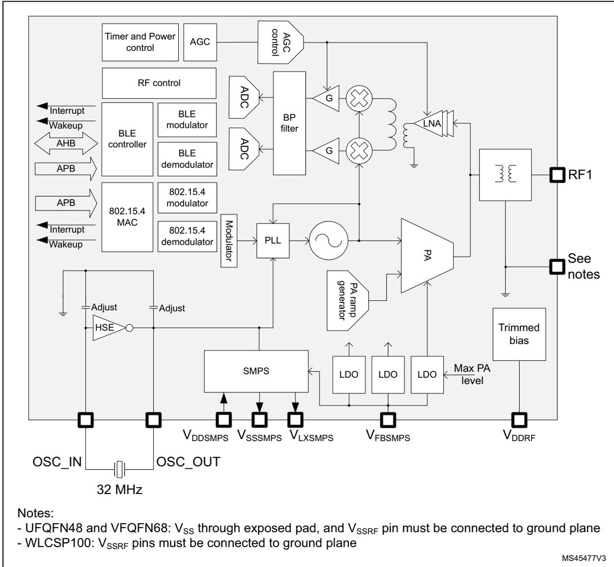
The block diagram illustrates the internal architecture of the radio system. At the top, 'Timer and Power control' and 'AGC' blocks are connected to an 'AGC control' block. Below this, 'RF control' connects to a 'BLE controller' and an '802.15.4 MAC'. The 'BLE controller' is linked to 'BLE modulator' and 'BLE demodulator' blocks, with 'Interrupt', 'Wakeup', and 'AHB' interfaces. The '802.15.4 MAC' is connected to '802.15.4 modulator' and '802.15.4 demodulator' blocks, with 'APB', 'Interrupt', and 'Wakeup' interfaces. Both modulators/demodulators feed into a 'Modulator' block, which connects to a 'PLL'. The 'PLL' is connected to a 'PA' (Power Amplifier) and a 'PA ramp generator'. The 'PA' output goes to an external 'RF1' pin through a matching network. A 'LNA' (Low Noise Amplifier) is connected to the 'RF1' path. A 'BP filter' (Band Pass Filter) is connected to the 'LNA' and has two 'ADC' blocks. The 'ADC' blocks also receive input from the 'AGC control'. An 'HSE' (High Speed External) oscillator with 'Adjust' pins is connected to 'OSC_IN' and 'OSC_OUT' pins, labeled '32 MHz'. Power management includes an 'SMPS' block connected to 'V_DDSMPS', 'V_SSSMPS', and 'V_LXSMPS' pins. Three 'LDO' blocks are connected to 'V_FBSMPS' pins, with one receiving 'Max PA level' input. A 'Trimmed bias' block is connected to 'V_DDRF' pins. A 'See notes' label is near the 'RF1' output.
Notes:
- - UFQFN48 and VFQFN68: V SS through exposed pad, and V SSRF pin must be connected to ground plane
- - WLCSP100: V SSRF pins must be connected to ground plane
MS45477V3
The maximum default transmit output power can be supported with a default V FBSMPS supply level. For higher output power the V FBSMPS supply level must be increased (see the device data sheet for more information).