2. System and memory overview
2.1 System architecture
The main system consists of 32-bit multilayer AHB bus matrix that interconnects:
- • Seven masters:
- – CPU1 (CPU1 Cortex ® -M4 with FPU) core I-bus
- – CPU1 (CPU1 Cortex ® -M4 with FPU) core D-bus
- – CPU1 (CPU1 Cortex ® -M4 with FPU) core S-bus
- – CPU2 (Cortex ® -M0+) core S-bus
- – DMA1
- – DMA2
- – Radio system
- • Ten slaves:
- – Internal Flash memory on the CPU1 (CPU1 Cortex ® -M4) ICode bus
- – Internal Flash memory on CPU1 (CPU1 Cortex ® -M4) DCode bus
- – Internal Flash memory on CPU2 (Cortex ® -M0+) S bus
- – Internal SRAM1 (up to 192 KB)
- – Internal SRAM2a (32 KB) + SRAM2b (32 KB)
- – AHB1 peripherals including AHB to APB bridges and APB peripherals (connected to APB1 and APB2)
- – AHB2 peripherals
- – Quad SPI memory interface (QUADSPI)
- – AHB4 shared peripheral
- – AHB5 including AHB to APB bridge and Radio peripherals (connected to APB3)
The bus matrix provides access from a master to a slave, enabling concurrent access and efficient operation even when several high-speed peripherals work simultaneously. This architecture is shown in Figure 1 .
Figure 1. System architecture
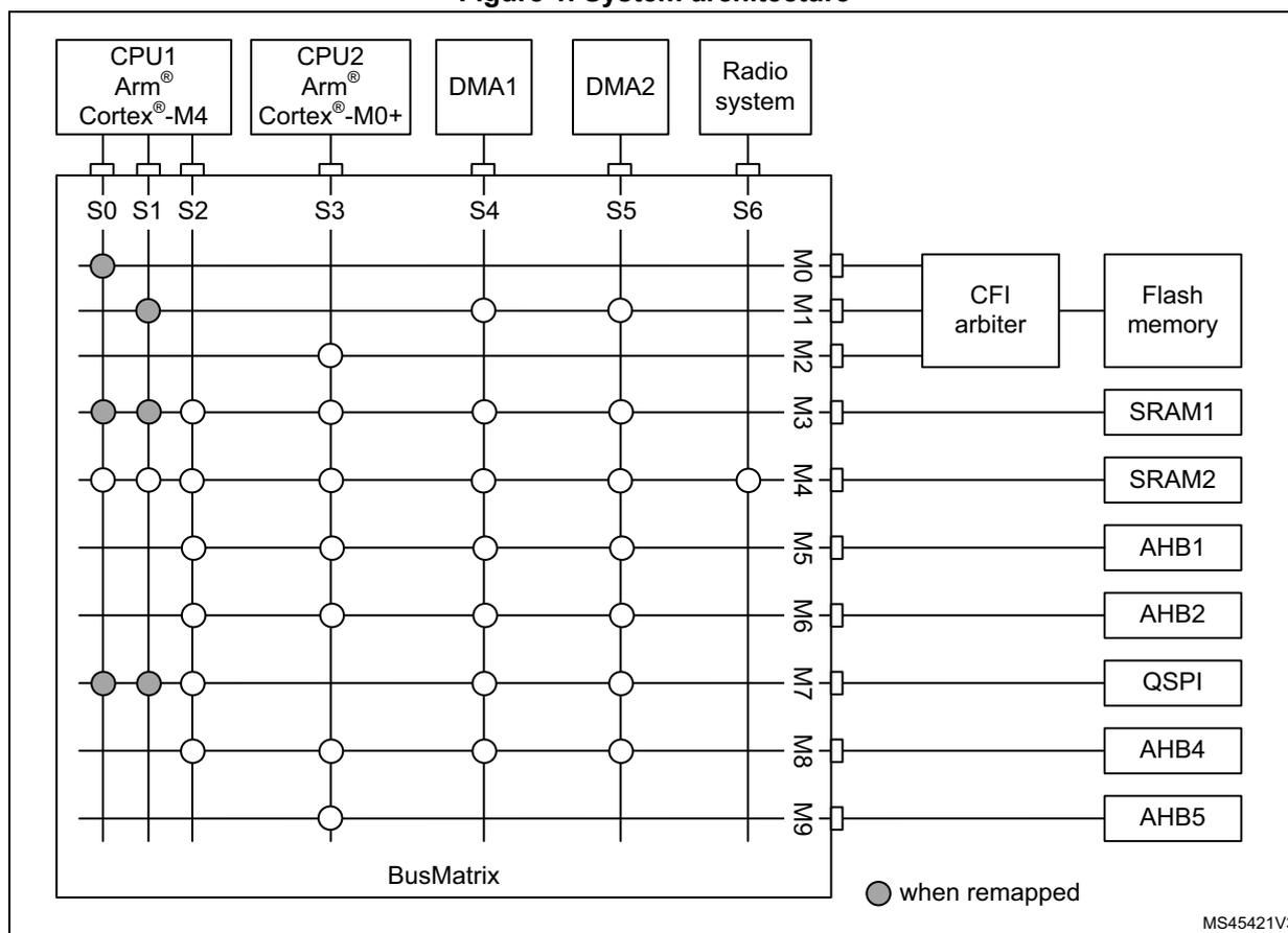
The diagram illustrates the system architecture centered around a BusMatrix. The BusMatrix has 10 slave ports (S0-S9) and 10 master ports (M0-M9). The connections are as follows:
- Slave Ports:
- S0, S1, S2: CPU1 Arm ® Cortex ® -M4
- S3: CPU2 Arm ® Cortex ® -M0+
- S4: DMA1
- S5: DMA2
- S6: Radio system
- Master Ports:
- M0: CFI arbiter
- M1: Flash memory
- M2: SRAM1
- M3: SRAM2
- M4: AHB1
- M5: AHB2
- M6: QSPI
- M7: AHB4
- M8: AHB5
- M9: (unlabeled)
- Connections:
- S0 connects to M0, M1, M2, M3, M4, M5, M6, M7, M8, M9.
- S1 connects to M0, M1, M2, M3, M4, M5, M6, M7, M8, M9 (with grey circles at M0, M1, M2, M3, M6, M7 indicating remapped connections).
- S2 connects to M0, M1, M2, M3, M4, M5, M6, M7, M8, M9 (with grey circles at M0, M1, M2, M3, M6, M7 indicating remapped connections).
- S3 connects to M0, M1, M2, M3, M4, M5, M6, M7, M8, M9.
- S4 connects to M0, M1, M2, M3, M4, M5, M6, M7, M8, M9.
- S5 connects to M0, M1, M2, M3, M4, M5, M6, M7, M8, M9.
- S6 connects to M0, M1, M2, M3, M4, M5, M6, M7, M8, M9.
Legend: ● when remapped
MS45421V3
2.1.1 S0: CPU1 (CPU1 Cortex ® -M4) I-bus
This bus connects the instruction bus of the CPU1 core to the BusMatrix. This bus is used by the core to fetch instructions. The targets of this bus are the internal Flash memory, SRAM1, SRAM2a (backup), SRAM2b (non backup) and the external memories through QUADSPI.
2.1.2 S1: CPU1 (CPU1 Cortex ® -M4) D-bus
This bus connects the data bus of the CPU1 core to the BusMatrix. This bus is used by the core for literal load and debug access. The targets of this bus are the internal Flash memory, SRAM1, SRAM2a (backup), SRAM2b (non backup) and the external memories through QUADSPI.
2.1.3 S2: CPU1 (CPU1 Cortex ® -M4) S-bus
This bus connects the system bus of the CPU1 core to the BusMatrix. This bus is used by the core to access data located in a peripheral or SRAM area. The targets of this bus are SRAM1, SRAM2a (backup), SRAM2b (non backup), the AHB1 peripherals including the APB1 and APB2 peripherals, the AHB2 peripherals, the AHB4 peripherals and the external memories through QUADSPI.
2.1.4 S3: CPU2 (Cortex ® -M0+) S-bus
This bus connects the system bus of the CPU2 core to the BusMatrix. This bus is used by the core to fetch instructions, for literal load and debug access, and access data located in a peripheral or SRAM area. The targets of this bus are the internal Flash memory, SRAM1, SRAM2a (backup), SRAM2b (non backup), the AHB1 peripherals including the APB1 and APB2 peripherals, the AHB2 peripherals, and the AHB4 peripherals and the AHB5 peripherals including the APB3 peripherals.
2.1.5 S4, S5: DMA-bus
This bus connects the AHB master interface of the DMA to the BusMatrix. The targets of this bus are the SRAM1, SRAM2a (backup), SRAM2b (non backup), the AHB1 peripherals including the APB1 and APB2 peripherals, the AHB2 peripherals, the AHB4 peripherals and the external memories through QUADSPI.
2.1.6 S6: Radio system-bus
This bus connects the AHB master interface of the Radio system to the BusMatrix. The targets of this bus are the SRAM2a (backup) and SRAM2b (non backup).
2.1.7 BusMatrix
The BusMatrix manages the access arbitration between masters. The arbitration uses a Round Robin algorithm. The BusMatrix is composed by seven masters (CPU1: system bus, DCode bus, ICode bus, CPU2: system bus, DMA1-bus, DMA2-bus and Radio system-bus) and ten slaves (3 x Flash memory, SRAM1, SRAM2a (backup), SRAM2b (non backup), AHB1 (including APB1 and APB2), AHB2, QUADSPI, AHB4, and AHB5).
AHB/APB bridges
The two bridges AHB to APB1 and AHB to APB2 provide full synchronous connections between the AHB and the two APB buses, allowing flexible selection of the peripheral frequency.
The bridges AHB to APB3 provide an a-synchronous connections between the AHB and the APB bus, allowing flexible selection of the frequency between the AHB and peripheral.
Refer to Section 2.2: Memory organization for the address mapping of the peripherals connected to this bridge.
After each device reset, all peripheral clocks are disabled (except for the SRAM1/2 and Flash memory interface). Before using a peripheral you have to enable its clock in the RCC_AHBxENR and the RCC_APBxENR registers.
Note: When a 16- or 8-bit access is performed on an APB register, the access is transformed into a 32-bit access: the bridge duplicates the 16- or 8-bit data to feed the 32-bit vector.
2.2 Memory organization
2.2.1 Introduction
Program memory, data memory, registers and I/O ports are organized within the same linear 4-Gbyte address space.
The bytes are coded in memory in Little Endian format. The lowest numbered byte in a word is considered the word's least significant byte and the highest numbered byte the most significant.
The addressable memory space is divided into eight main blocks, of 512 Mbytes each.
2.2.2 Memory map and register boundary addresses
Figure 2. Memory map
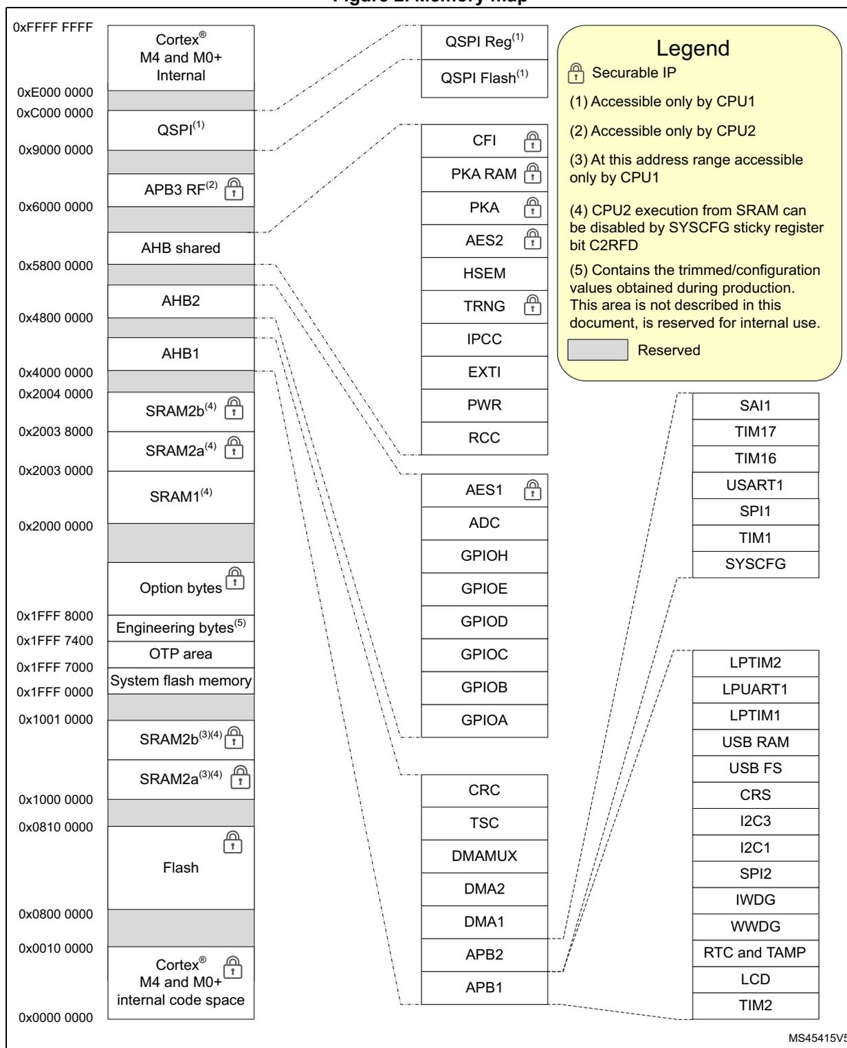
Legend
- Securable IP
- (1) Accessible only by CPU1
- (2) Accessible only by CPU2
- (3) At this address range accessible only by CPU1
- (4) CPU2 execution from SRAM can be disabled by SYSCFG sticky register bit C2RFD
- (5) Contains the trimmed/configuration values obtained during production. This area is not described in this document, is reserved for internal use.
- Reserved
Memory Map Details:
- 0xFFFF FFFF to 0xE000 0000: Cortex® M4 and M0+ Internal
- 0xE000 0000 to 0xC000 0000: Reserved
- 0xC000 0000 to 0x9000 0000: QSPI (1)
- 0x9000 0000 to 0x8000 0000: Reserved
- 0x8000 0000 to 0x6000 0000: APB3 RF (2)
- 0x6000 0000 to 0x5800 0000: Reserved
- 0x5800 0000 to 0x4800 0000: AHB shared
- 0x4800 0000 to 0x4000 0000: AHB2
- 0x4000 0000 to 0x2004 0000: Reserved
- 0x2004 0000 to 0x2003 8000: SRAM2b (4)
- 0x2003 8000 to 0x2003 0000: SRAM2a (4)
- 0x2003 0000 to 0x2000 0000: SRAM1 (4)
- 0x2000 0000 to 0x1FFF 8000: Reserved
- 0x1FFF 8000 to 0x1FFF 7400: Option bytes
- 0x1FFF 7400 to 0x1FFF 7000: Engineering bytes (5)
- 0x1FFF 7000 to 0x1FFF 0000: OTP area
- 0x1FFF 0000 to 0x1001 0000: System flash memory
- 0x1001 0000 to 0x1000 0000: Reserved
- 0x1000 0000 to 0x0810 0000: SRAM2b (3)(4)
- 0x0810 0000 to 0x0800 0000: SRAM2a (3)(4)
- 0x0800 0000 to 0x0010 0000: Flash
- 0x0010 0000 to 0x0000 0000: Cortex® M4 and M0+ internal code space
Peripheral Register Blocks:
- QSPI Reg (1) and QSPI Flash (1) (linked to 0xC000 0000 - 0x9000 0000)
- CFI , PKA RAM , PKA , AES2 , HSEM , TRNG , IPCC , EXTI , PWR , RCC (linked to 0x9000 0000 - 0x8000 0000)
- AES1 , ADC , GPIOH , GPIOE , GPIO D , GPIOC , GPIOB , GPIOA (linked to 0x8000 0000 - 0x6000 0000)
- CRC , TSC , DMAMUX , DMA2 , DMA1 , APB2 , APB1 (linked to 0x6000 0000 - 0x4800 0000)
- SAI1 , TIM17 , TIM16 , USART1 , SPI1 , TIM1 , SYSCFG (linked to 0x4000 0000 - 0x2000 0000)
- LPTIM2 , LPUART1 , LPTIM1 , USB RAM , USB FS , CRS , I2C3 , I2C1 , SPI2 , IWDG , WWDG , RTC and TAMP , LCD , TIM2 (linked to 0x2000 0000 - 0x1000 0000)
MS45415V5
- It is forbidden to access QUADSPI Flash bank area before having properly configured and enabled the QUADSPI peripheral.
All the memory areas not allocated to on-chip memories and peripherals are considered “Reserved”. For the detailed mapping of available memory and register areas, refer to the following table, which gives the boundary addresses of the available peripherals.
Table 1. Memory map and peripheral register boundary addresses
| Bus | Boundary address | Size (bytes) | Peripheral | Peripheral register map |
|---|---|---|---|---|
| AHB3 | 0xA000 1000 - 0xA000 13FF | 1 K | QUADSPI | Section 18.5.14: QUADSPI register map on page 457 |
| 0xA000 0000 - 0xA000 0FFF | 4 K | Reserved | - | |
| 0x9000 0000 - 0x9FFF FFFF | 256 M | QUADSPI Flash | - | |
| - | 0x6000 2000 - 0x8FFF FFFF | - | Reserved | - |
| APB3 | 0x6000 1000 - 0x6000 1FFF | 4 K | 802.15.4 CTRL | - |
| 0x6000 0800 - 0x6000 0FFF | 2 K | Reserved | - | |
| 0x6000 0400 - 0x6000 07FF | 1 K | Radio CTRL | - | |
| 0x6000 0000 - 0x6000 03FF | 1 K | BLE CTRL | - | |
| AHB4 | 0x5800 4400 - 0x5FFF FFFF | 128 K | Reserved | - |
| 0x5800 4000 - 0x5800 43FF | 1 K | FLASH | Section 3.10.20: FLASH register map on page 129 | |
| 0x5800 3400 - 0x5800 3FFF | 3 K | Reserved | - | |
| 0x5800 2400 - 0x5800 33FF | 5 K | PKA RAM | Section 26.7.5: PKA register map on page 702 | |
| 0x5800 2000 - 0x5800 23FF | PKA | |||
| 0x5800 1C00 - 0x5800 1FFF | 1 K | Reserved | - | |
| 0x5800 1800 - 0x5800 1BFF | 1 K | AES2 | Section 25.7.18: AES register map on page 675 | |
| 0x5800 1400 - 0x5800 17FF | 1 K | HSEM | Section 8.4.9: HSEM register map on page 302 | |
| 0x5800 1000 - 0x5800 13FF | 1 K | True RNG | Section 24.7.4: RNG register map on page 627 | |
| 0x5800 0C00 - 0x5800 0FFF | 1 K | IPCC | Section 9.4.9: IPCC register map on page 317 | |
| 0x5800 0800 - 0x5800 0BFF | 1 K | EXTI | Section 16.6.17: EXTI register map on page 424 | |
| 0x5800 0400 - 0x5800 07FF | 1 K | PWR | Section 5.6.24: PWR register map and reset value table on page 187 | |
| 0x5800 0000 - 0x5800 03FF | 1 K | RCC | Section 6.4.49: RCC register map on page 272 |
Table 1. Memory map and peripheral register boundary addresses (continued)
| Bus | Boundary address | Size (bytes) | Peripheral | Peripheral register map |
|---|---|---|---|---|
| AHB2 | 0x5006 0400 - 0x57FF FFFF | - | Reserved | - |
| 0x5006 0000 - 0x5006 03FF | 1 K | AES1 | Section 25.7.18: AES register map on page 675 | |
| 0x5004 0000 - 0x5004 03FF | 1 K | ADC | Section 19.9: ADC register map on page 547 | |
| 0x4800 1C00 - 0x4800 1FFF | 1 K | GPIOH | Section 10.5.12: GPIO register map on page 335 | |
| 0x4800 1400 - 0x4800 1BFF | 3 K | Reserved | - | |
| 0x4800 1000 - 0x4800 13FF | 1 K | GPIOE | Section 10.5.12: GPIO register map on page 335 | |
| 0x4800 0C00 - 0x4800 0FFF | 1 K | GPIOF | ||
| 0x4800 0800 - 0x4800 0BFF | 1 K | GPIOC | ||
| 0x4800 0400 - 0x4800 07FF | 1 K | GPIOB | ||
| 0x4800 0000 - 0x4800 03FF | 1 K | GPIOA | ||
| AHB1 | 0x4002 4400 - 0x47FF FFFF | 127 M | Reserved | - |
| 0x4002 4000 - 0x4002 43FF | 1 K | TSC | Section 23.6.11: TSC register map on page 613 | |
| 0x4002 3400 - 0x4002 3FFF | 3 K | Reserved | - | |
| 0x4002 3000 - 0x4002 33FF | 1 K | CRC | Section 17.4.6: CRC register map on page 432 | |
| 0x4002 0C00 - 0x4002 2FFF | 9 K | Reserved | - | |
| 0x4002 0800 - 0x4002 0BFF | 1 K | DMAMUX | Section 14.6.7: DMAMUX register map on page 395 | |
| 0x4002 0400 - 0x4002 07FF | 1 K | DMA2 | Section 13.6.7: DMA register map on page 378 | |
| 0x4002 0000 - 0x4002 03FF | 1 K | DMA1 | ||
| - | 0x4001 5800 - 0x4001 FFFF | 42 K | Reserved | - |
Table 1. Memory map and peripheral register boundary addresses (continued)
| Bus | Boundary address | Size (bytes) | Peripheral | Peripheral register map |
|---|---|---|---|---|
| APB2 | 0x4001 5400 - 0x4001 57FF | 1 K | SAI1 | Section 39.6.19: SAI register map on page 1312 |
| 0x4001 4C00 - 0x4001 53FF | 2 K | Reserved | - | |
| 0x4001 4800 - 0x4001 4BFF | 1 K | TIM17 | Section 29.4.23: TIM16/TIM17 register map on page 926 | |
| 0x4001 4400 - 0x4001 47FF | 1 K | TIM16 | Section 29.4.23: TIM16/TIM17 register map on page 926 | |
| 0x4001 3C00 - 0x4001 43FF | 2 K | Reserved | - | |
| 0x4001 3800 - 0x4001 3BFF | 1 K | USART1 | Section 36.8.15: USART register map on page 1158 | |
| 0x4001 3400 - 0x4001 37FF | 1 K | Reserved | - | |
| 0x4001 3000 - 0x4001 33FF | 1 K | SPI1 | Section 38.6.8: SPI register map on page 1247 | |
| 0x4001 2C00 - 0x4001 2FFF | 1 K | TIM1 | Section 27.4.30: TIM1 register map on page 801 | |
| 0x4001 0400 - 0x4001 2BFF | 10 K | Reserved | - | |
| 0x4001 0200 - 0x4001 03FF | 1 K | COMP | Section 21.6.3: COMP register map on page 566 | |
| 0x4001 0100 - 0x4001 01FF | SYSCFG | Section 11.2.17: SYSCFG register map on page 352 | ||
| 0x4001 0030 - 0x4001 00FF | VREFBUF | Section 20.5.3: VREFBUF register map on page 553 | ||
| 0x4001 0000 - 0x4001 002F | SYSCFG | Section 11.2.17: SYSCFG register map on page 352 |
Table 1. Memory map and peripheral register boundary addresses (continued)
| Bus | Boundary address | Size (bytes) | Peripheral | Peripheral register map |
|---|---|---|---|---|
| APB1 | 0x4000 9800 - 0x4000 FFFF | 26 K | Reserved | - |
| 0x4000 9400 - 0x4000 97FF | 1 K | LPTIM2 | Section 30.7.11: LPTIM register map on page 952 | |
| 0x4000 8400 - 0x4000 93FF | 4 K | Reserved | - | |
| 0x4000 8000 - 0x4000 83FF | 1 K | LPUART1 | Section 37.7.13: LPUART register map on page 1211 | |
| 0x4000 7C00 - 0x4000 7FFF | 1 K | LPTIM1 | Section 30.7.11: LPTIM register map on page 952 | |
| 0x4000 7000 - 0x4000 7BFF | 3 K | Reserved | - | |
| 0x4000 6C00 - 0x4000 6FFF | 1K | USB SRAM | Section 40.6.3: USB register map on page 1345 | |
| 0x4000 6800 - 0x4000 6BFF | 1 K | USB FS | Section 40.6.3: USB register map on page 1345 | |
| 0x4000 6400 - 0x4000 67FF | 1 K | Reserved | - | |
| 0x4000 6000 - 0x4000 63FF | 1 K | CRS | Section 7.7.5: CRS register map on page 288 | |
| 0x4000 5C00 - 0x4000 5FFF | 1 K | I2C3 | Section 35.9.12: I2C register map on page 1073 | |
| 0x4000 5800 - 0x4000 5BFF | 1 K | Reserved | - | |
| 0x4000 5400 - 0x4000 57FF | 1 K | I2C1 | Section 35.9.12: I2C register map on page 1073 | |
| 0x4000 3C00 - 0x4000 53FF | 6 K | Reserved | - | |
| 0x4000 3800 - 0x4000 3BFF | 1 K | SPI2 | Section 38.6.8: SPI register map on page 1247 | |
| 0x4000 3400 - 0x4000 37FF | 1 K | Reserved | - | |
| 0x4000 3000 - 0x4000 33FF | 1 K | IWDG | Section 32.4.6: IWDG register map on page 962 | |
| 0x4000 2C00 - 0x4000 2FFF | 1 K | WWDG | Section 33.5.4: WWDG register map on page 968 | |
| 0x4000 2800 - 0x4000 2BFF | 1 K | RTC & TAMP | Section 34.7.21: RTC register map on page 1009 | |
| 0x4000 2400 - 0x4000 27FF | 1 K | LCD | Section 22.6.8: LCD register map on page 595 | |
| 0x4000 0400 - 0x4000 23FF | 8 K | Reserved | - | |
| 0x4000 0000 - 0x4000 03FF | 1 K | TIM2 | Section 28.4.25: TIMx register map on page 873 | |
| AHB4 | 0x2003 8000 - 0x2003 FFFF | 32 K | SRAM2b | - |
| 0x2003 0000 - 0x2003 7FFF | 32 K | SRAM2a | - | |
| 0x2000 3000 - 0x2002 FFFF | 180 K | Reserved | - | |
| AHB1 | 0x2000 0000 - 0x2000 2FFF | 192 (1) K | SRAM1 | - |
| Bus | Boundary address | Size (bytes) | Peripheral | Peripheral register map |
|---|---|---|---|---|
| AHB4 | 0x1FFF 8000 - 0x1FFF 807F | 128 B | Flash memory options | Section 3.10.20: FLASH register map on page 129 |
| 0x1FFF 7000 - 0x1FFF 73FF | 1 K | Flash memory OTP | - | |
| 0x1FFF 0000 - 0x1FFF 6FFF | 28 K | Flash memory boot loader | - | |
| 0x1000 0000 - 0x1000 FFFF | 64 K | SRAM2a/b CPU1 mirror | - | |
| 0x0800 0000 - 0x080F FFFF | 1 M (1) | User flash memory | - | |
| (2) | 0x0000 0000 - 0x000F FFFF | 1 M (1) | CPUUn boot area | - |
1. Depends upon device, see the product datasheet.
2. Bus depends upon selected CPUUn Boot area.
2.2.3 Bit banding
The CPU1 map includes two bit-band regions. These regions map each word in an alias region of memory to a bit in a bit-band region of memory. writing to a word in the alias region has the same effect as a read-modify-write operation on the targeted bit in the bit-band region.
The AHB1, APB1, APB2 peripheral registers and the SRAM1, SRAM2a and SRAM2b are mapped to a bit-band region, hence single bit-band write and read operations are allowed. The operations are only available for CPU1 accesses, and not form other bus masters (e.g. DMA)
The peripheral bit-band alias is located from address 0x4200 0000 to 0x42FF FFFF
The SRAM bit-band alias is located from address 0x2200 0000 to 0x227F FFFF
A mapping formula shows how to reference each word in the alias region to a corresponding bit in the bit-band region. The mapping formula is:
\( \text{bit\_word\_addr} = \text{bit\_band\_base} + (\text{byte\_offset} * 32) + (\text{bit\_number} * 4) \) , where:
- – \( \text{bit\_word\_addr} \) is the address of the word in the alias memory region that maps to the targeted bit.
- – \( \text{bit\_band\_base} \) is the starting address of the alias region
- – \( \text{byte\_offset} \) is the number of the byte in the bit_band region that contains the targeted bit
- – \( \text{bit\_number} \) is the bit position (0-7) of the targeted bit
Example
The following example shows how to map bit [2] of the byte located at SRAM1 address 0x2000 0300 to the alias region.
Writing to address 0x2200 6008 has the same effect as a read-modify-write operation on bit [2] of the byte at SRAM1 address 0x2000 0300.
Reading address 0x2200 6008 returns the value 0x01 or 0x00 of bit [2] of the byte at SRAM1 address 0x2000 0300.
For more information on bit-band, refer to the Cortex ® -M4 programming manual.
2.3 Boot configuration
Three different CPU1 boot modes can be selected through the BOOT0 pin and nBOOT1 bit in the User options, as shown in Table 2 .
Table 2. Boot modes
| nBOOT1 FLASH_OPTR[23] | nBOOT0 FLASH_OPTR[27] | BOOT0 pin PH3 | nSWBOOT0 FLASH_OPTR[26] | Main flash empty (1) | Boot memory space alias |
|---|---|---|---|---|---|
| x | x | 0 | 1 | 0 | Main flash memory is selected as boot area |
| x | x | 0 | 1 | 1 | System memory is selected as boot area |
| x | 1 | x | 0 | x | Main flash memory is selected as boot area |
| 0 | x | 1 | 1 | x | Embedded SRAM1 is selected as boot area |
| 0 | 0 | x | 0 | x | |
| 1 | x | 1 | 1 | x | System memory is selected as boot area |
| 1 | 0 | x | 0 | x |
- 1. A flash empty check mechanism is implemented to force the boot from system flash if the first flash memory location is not programmed (0xFFFF FFFF) and if the boot selection was configured to boot from the main flash.
The values on both BOOT0 and BOOT1 are latched after a reset. It is up to the user to provide the correct value for the required boot mode.
The BOOT0 and BOOT1 are also re-sampled when exiting Standby mode. Consequently they must be kept in the required boot mode. After the startup delay, the CPU1 fetches the top-of-stack from address 0x0000 0000, then starts code execution from the boot memory at 0x0000 0004.
Depending on the selected boot mode, main flash, system flash, or SRAM1 memories are accessible as follows:
- • Boot from main flash memory: the main flash memory is aliased in the CPU1 boot memory space at address 0x0000 0000, and is accessible even from its physical address 0x0800 0000. In other words, the flash memory content can be accessed starting from address 0x0000 0000 or 0x0800 0000.
- • Boot from system flash memory: the system flash memory is aliased in the CPU1 boot memory space at address 0x0000 0000, and is also still accessible from its physical address 0x1FFF 0000.
- • Boot from SRAM: the memory is aliased in the CPU1 boot memory space at address 0x0000 0000, and is accessible even from its physical address 0x2000 0000.
Empty check
An internal empty check flag (the EMPTY bit of the FLASH access control register (FLASH_ACR)) is available for easy programming of virgin devices by the boot loader. This flag is used when BOOT0 pin is defining main flash as the target boot area. When the flag is set, the device is considered as empty, and the system memory (boot loader) is selected instead of the main flash as a boot area, to allow user to program the memory. Therefore, some of the GPIOs are reconfigured from the high-Z state. Refer to AN2606 for more details concerning the bootloader and GPIO configuration in system memory boot mode. It is possible to disable this feature by configuring the option bytes to force boot from the main flash memory (nSWBOOT0 = 0, nBOOT0 = 1).
This empty check flag is updated only during the loading of option bytes: it is set when the content of the address 0x08000 0000 is read as 0xFFFF FFFF, otherwise it is cleared. A power reset or setting the OBL_LAUNCH bit in FLASH_CR register is needed to clear this flag after programming of a virgin device, to execute user code after System reset. The EMPTY bit can be written directly by software.
CPU1 physical remap
Following CPU1 boot the application software can modify the memory map at address 0x0000 0000. This modification is performed by programming the SYSCFG memory remap register (SYSCFG_MEMRMP) in the SYSCFG controller.
The following memories can be remapped:
- • Main flash memory
- • System flash memory
- • SRAM
- • Quad SPI memory
Embedded boot loader
The embedded boot loader is located in the system flash memory, programmed by ST during production. It is used to program the flash memory using one of the following device interfaces:
- • USART1 on pins PA9 and PA10
- • I2C1 on pins PB6 and PB7.
- • I2C3 on pins PC0 and PC1
- • SPI1 on pins PA4, PA5, PA6 and PA7
- • SPI2 on pins PB12, PB13, PB14 and PB15
- • USB FS on pins PA11 and PA12.
2.4 CPU2 boot
Following a device reset the CPU2 will only boot after CPU1 has set the C2BOOT bit in the PWR control register 4 (PWR_CR4) . The C2BOOT value is retained in Standby mode and the CPU2 will boot accordingly when exit from Standby.
The CPU2 will boot from its boot reset vector as defined by the flash user option C2OPT and SBRV.
The CPU2 may boot from anywhere in user flash or SRAM1/SRAM2a/SRAM2b.
CPU2 safe boot
When, after a reset, the User options are not valid and the BOOT0 and BOOT1 select CPU1 to boot from main flash memory, the CPU2 boots from a safe boot vector in main flash memory at address 0x080F F000.
The safe boot can be used to restore the last known user options from an copied image.
2.5 CPU2 SRAM fetch disable
CPU2 execution from SRAM can be disabled by the C2RFD bit in SYSCFG register. Disabling CPU2 execution from SRAM improves robustness of the CPU2 software.