54. Management data input/output (MDIOS)
54.1 MDIOS introduction
An MDIO bus can be useful in systems where a master chip needs to manage (configure and get status data from) one or multiple slave chips. The bus protocol uses only two signals:
- • MDC: the management data clock
- • MDIO: the data line carrying the opcode (write or read), the slave (port) address, the MDIOS register address, and the data
In each transaction, the master either reads the contents of an MDIOS register in one of its slaves, or it writes data to an MDIOS register in one of its slaves.
The MDIOS peripheral serves as a slave interface to a MDIO bus. A MDIO master can use the MDC/MDIO lines to write and read 32 16-bit MDIOS registers, which are held in the MDIOS. These MDIOS registers are managed by the firmware. This allows the MDIO master to configure the application running on the STM32 and get status information from it.
The MDIOS can operate in Stop mode, optionally waking up the STM32 if the MDIO master performs a read or a write to one of its MDIOS registers.
54.2 MDIOS main features
The MDIOS includes the following features:
- • 32 MDIOS register addresses, each of which is managed using separate input and output data registers:
- – 32 x 16-bit firmware read/write, MDIOS read-only output data registers
- – 32 x 16-bit firmware read-only, MDIOS write-only input data registers
- • Configurable slave (port) address
- • Independently maskable interrupts/events:
- – MDIOS register write
- – MDIOS register read
- – MDIOS protocol error
- • Able to operate in and wake up from Stop mode
54.3 MDIOS functional description
54.3.1 MDIOS block diagram
Figure 696. MDIOS block diagram
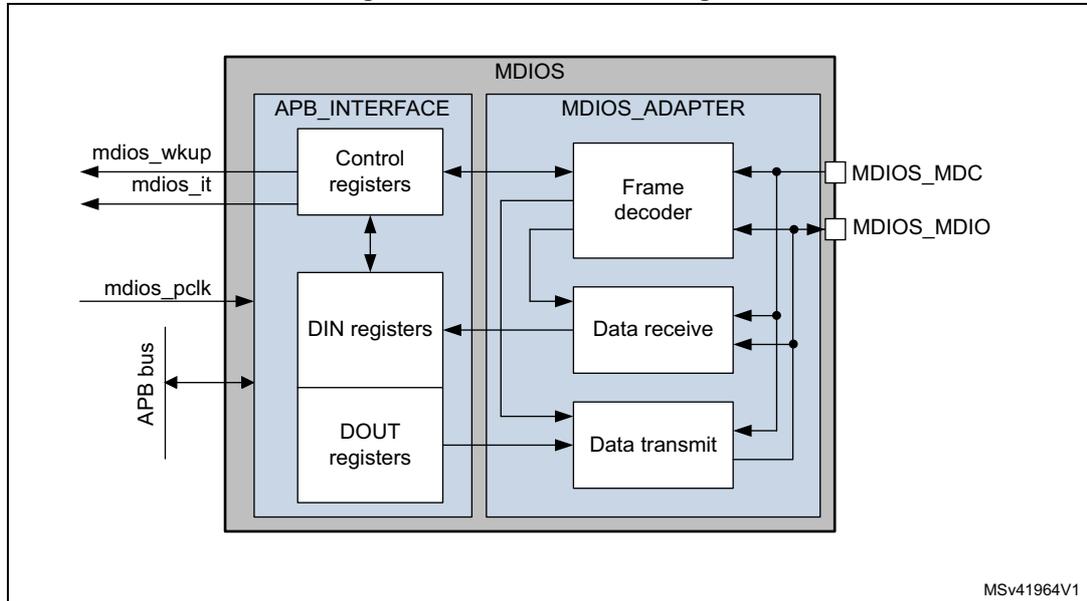
54.3.2 MDIOS pins and internal signals
Table 447 lists the MDIOS inputs and output signals connected to package pins or balls, while Table 448 shows the internal PWR signals.
Table 447. MDIOS input/output signals connected to package pins or balls
| Signal name | Signal type | Description |
|---|---|---|
| MDIOS_MDC | Digital input | MDIO master clock |
| MDIOS_MDIO | Digital input/output | MDIO signal (opcode, address, input/output data) |
Table 448. MDIOS internal input/output signals
| Signal name | Signal type | Description |
|---|---|---|
| mdios_wkup | Digital output | MDIOS wake-up signal |
| mdios_it | MDIOS interrupt signal | |
| mdios_pclk | Digital input | APB clock |
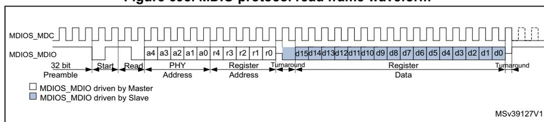
54.3.3 MDIOS protocol
The MDIOS protocol uses two signals:
- • MDIOS_MDC: the clock, always driven by the master
- • MDIOS_MDIO: signal carrying the opcode, address, and bidirectional data
Each transaction is performed using a frame, which contains 32 bits (each passed serially):
- • 14 control bits, driven by the master
- – 2 start bits: always 01
- – 2 opcode bits: read = 10, write = 01
- – 5 port address bits, indicating which slave device is being addressed
- – 5 MDIOS register address bits, up to 32 MDIOS registers can be addressed in each slave
- • 2 turnaround state bits
- – On write operations, the master drives 10
- – On read operations, the first bit is high-impedance, and the second bit is driven by the slave to 0
- • 16 data bits
- – On write operations, data written to slave MDIOS register is driven by the master
- – On read operations, data read from slave MDIOS register is driven by the slave
Each frame is usually preceded by a preamble, where the MDIO stays at one for 32 MDC clocks. The master can continue to keep MDIO at one, indicating the idle condition, when it has no frame to send.
When MDIO signal is driven by the master, MDIOS samples it using the rising edge of MDC. When MDIOS drives MDIO, the output changes on the rising edge of MDC.
Figure 697. MDIO protocol write frame waveform
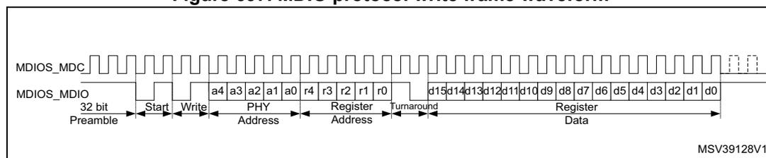
Figure 698. MDIO protocol read frame waveform
54.3.4 MDIOS enabling and disabling
The MDIOS is enabled by setting the EN bit in MDIOS_CR. When EN = 1, the MDIOS monitors the MDIO bus and service frames addressed to one of its MDIOS registers.
When the MDIOS is enabled (setting EN to one), the same write operation to MDIOS_CR must properly set the PORT_ADDRESS[4:0] field to indicate the slave port address. A frame is ignored by the MDIOS if its port address is not the same as PORT_ADDRESS[4:0] (presumably intended for another slave).
When EN = 0, the MDIOS ignores the frames being transmitted on the MDC/MDIO lines, and the IP is in a reduced consumption mode. Clearing EN also clears all of the DIN registers. If EN is cleared while the MDIOS is driving read data, it immediately releases the bus and does not drive the rest of the data. If EN is cleared while the MDIOS is receiving a frame, the frame is aborted and the data is lost.
When the MDIOS is enabled, disabled and reenabled, the status flags are not cleared. For a correct operation, the firmware must clear the status flag before reenabling the MDIOS.
54.3.5 MDIOS data
From the point of view of the MDIO master, there are 32 16-bit MDIOS registers in the MDIOS, which can be written and read. In reality, for each MDIOS register 'x' there are two sets of registers: MDIOS_DINRx and MDIOS_DOUTRx.
Input data
When the MDIO master transmits a frame, which writes to MDIOS register 'x' in the MDIOS, it is MDIOS_DINRx, which is updated with the incoming data. The registers MDIOS_DINR0 to MDIOS_DINR31 can be read by the firmware, but they can be written only by the MDIO master via the MDIO bus.
The contents of MDIOS_DINRx change immediately after the MDC rising edge when the last data bit is sampled.
If the firmware happens to read the contents of MDIOS_DINRx at the moment that it is being updated, there is a possibility that the value read is corrupted (a bit-by-bit cross between the old value and the new value). For this reason, the firmware must assure that two subsequent reads from the same MDIOS_DINRx give the same value and assure that the data is stable when it is read . In the very worst case, the firmware needs to read four times MDIOS_DINRx to:
- 1. Get the old value
- 2. Get an incoherent value (when reading at the moment the register changes)
- 3. Get the new value
- 4. Confirm the new value
If the firmware uses the WRF interrupt and can guarantee that it reads the MDIOS_DINRx register before any new MDIOS write frame completes, the firmware can perform a single read.
If the MDIO master performs a write operation with a register address, which is greater than 31, the MDIOS ignores the frame (the data is not saved and no flag is set).
Output data
When the MDIOS receives a frame, which requests to read register 'x', it returns the value found in MDIOS_DOUTRx. Thus, if the MDIO master expects to read the same value, which it previously wrote to MDIOS register 'x', the firmware must copy the data from MDIOS_DINRx to MDIOS_DOUTRx each time new data is written to MDIOS_DINRx. For correct operation, the firmware must copy the data to the MDIOS_DOUTRx register within a preamble (if the master sends preambles before each frame) plus 15 cycles time.
When an MDIOS register is read via the MDIO bus, the MDIOS passes the 16-bit value (from the corresponding MDIOS_DOUTRx) to the MDIOS clock domain during the 15 th cycle of the read frame. If the firmware attempts to write MDIOS_DOUTRx while the MDIO
master is currently reading MDIOS register 'x', the firmware write operation is ignored if it occurs during the 15 th cycle of the frame (during a one-MDC-cycle window). Therefore, after writing MDIOS_DOUTRx, the firmware must read back the same MDIOS_DOUTRx and confirm that the value was actually written. If MDIOS_DOUTRx does not contain the value, which was written, the firmware can simply try writing and rereading again.
If the MDIOS frequency is very slow compared to the mdios_pclk frequency, it is better not to tie up the CPU by continuously writing and rereading MDIOS_DOUTRx.
Note: The read flag (RDFx) is set as soon as the MDIOS_DOUTRx DOUT[15:0] value is passed to the MDIOS clock domain. Thus, when a write to MDIOS_DOUTRx is ignored (when the value read back is not the value, which was just written), the firmware can use a read interrupt to know when it is able to write MDIOS_DOUTRx.
Respect the following procedure if the MDC clock is very slow:
- 1. Write MDIOS_DOUTRx.
- 2. Assure that all of the read flags are zero (MDIOS_RDFR = 0x0000). Clear the flags if necessary using MDIOS_CRDFR.
- 3. Read back the same MDIOS_DOUTRx and compare the value with the value, which was written in step 1.
- 4. If the values are the same, the procedure is done. Otherwise, continue to step 5.
- 5. Enable read interrupts by setting the RDIE bit in MDIOS_CR1.
- 6. In the interrupt routine, assure that RDFx is set (no other read flags are set before bit x).
- 7. There is a 31 cycle + preamble time window (if the master sends a preamble before each frame) to write MDIOS_DOUTRx safely without doing a read-back and compare. If this maximum delay cannot be guaranteed, go back to step 1.
If the MDIO master performs a read operation with a register address, which is greater than 31, the MDIOS returns a data value of all zeros.
54.3.6 MDIOS APB frequency
Whenever the firmware reads from MDIOS_DINRx or writes to MDIOS_DOUTRx, the frequency of the APB bus must be at least 1.5 times the MDC frequency. For example, if MDC is at 20 MHz, the APB must be at 30 MHz or faster.
54.3.7 Write/read flags and interrupts
When MDIOS register 'x' is written via the MDIO bus, the WRFx bit in MDIOS_WRFR is set. WRFx becomes one at the moment that MDIOS_DINRx is updated, which is when the last data bit is sampled on a write frame. An interrupt is generated if WRIEN = 1 (in MDIOS_CR). WRFx is cleared by software by writing 1 to CWRFx (in MDIOS_CWRFR).
When MDIOS register 'x' is read via the MDIO bus, the RDFx bit in MDIOS_RDFR is set. RDFx becomes one at the moment that MDIOS_DOUTRx is copied to the MDC clock domain, which is on the 15 th cycle of a read frame. An interrupt is generated if RDIEN = 1 (in MDIOS_CR). RDFx is cleared by software by writing 1 to CRDFx (in MDIOS_CRDFR).
54.3.8 MDIOS error management
There are three types of errors with their corresponding error flags:
- • Preamble error: PERF (bit 0 of MDIOS_SR)
- • Start error: SERF (bit 1 of MDIOS_SR)
- • Turnaround error: TERF (bit 2 of MDIOS_SR)
Each error flag is set by hardware when the corresponding error condition occurs. Each flag can be cleared by writing '1' to the corresponding bit in the clear flag register (MDIOS_CLRFR).
An interrupt occurs if any of the three error flags is set while EIE = 1 (MDIOS_CR).
Besides, setting an error flag, the MDIOS performs no action for a frame in which an error is detected: MDIOS_DINRx are not updated and the MDIO line is not forced during the data phase.
For a given frame, errors do not accumulate. For example, if a preamble error is detected, no check is done for a start error or a turnaround error for the rest of the current frame.
When DPC = 0, following a detected error, all new frames, and errors are ignored until a complete full preamble has been detected.
When DPC = 1 (disable preamble check, MDIOS_CR[7]), all frames and new errors are ignored as long as one of the error flags is set. As soon as the error bit is cleared, the MDIOS starts looking for a start sequence. Thus, the application must clear the error flag only when it is sure that no frame is currently in progress. Otherwise, the MDIOS likely misinterprets the bits being sent and becomes desynchronized with the master.
Preamble errors
A preamble error occurs when a start sequence begins (with MDIO sampled at 0) without being immediately preceded by a preamble (MDIO sampled at 1 for at least 32 consecutive clocks).
Preamble errors are not reported after the MDIOS is first enabled (EN = 1 in MDIOS_CR) until after a full preamble is received. This is to avoid an error condition when the peripheral frame detection is enabled while a preamble or frame is already in progress. In this case, the MDIOS ignores the first frame (since it did not first detect a full preamble), but does not set PERF.
If the DPC bit (disable preamble check, MDIOS_CR[7]) is set, the MDIO master can send frames without preceding preambles and no preamble error is signaled. When DPC = 1, the application must assure that the master is not in the process of sending a frame at the moment that the MDIOS is enabled (EN is set). Otherwise, the slave might become desynchronized with the master.
Start errors
A start error occurs when an illegal start sequence occurs or if an illegal command is given. The start sequence must always be 01, and the command must be either 01 (write) or 10 (read).
As with preamble errors, start errors are not reported until after a full preamble is received.
Turnaround errors
A turnaround error occurs when an error is detected in the turnaround bits of write frames. The 15 th bit of the write frame must be 1 and the 16 th bit must be 0.
Turnaround errors are only reported after a full preamble is received, there is no start error, the port address in the current frame matches, and the register address is in the supported range 0 to 31.
54.3.9 MDIOS in Stop mode
The MDIOS can operate in Stop mode, responding to all reads, performing all writes, and causing the STM32 to wake up from Stop mode on MDIOS interrupts.
54.3.10 MDIOS interrupts
There is a single interrupt vector for the three types of interrupts (write, read, and error). Any of these interrupt sources can wake the STM32 up from Stop mode. All interrupt flags need to be cleared in order to clear the interrupt line.
Table 449. Interrupt control bits
| Interrupt event | Event flag | Enable control bit |
|---|---|---|
| Write interrupt | WRF[31:0] | WRIE |
| Read interrupt | RDF[31:0] | RDIE |
| Error interrupt | PERF (preamble), SERF (start), TERF (turnaround) | EIE |
54.4 MDIOS registers
54.4.1 MDIOS configuration register (MDIOS_CR)
Address offset: 0x000
Reset value: 0x0000 0000
| 31 | 30 | 29 | 28 | 27 | 26 | 25 | 24 | 23 | 22 | 21 | 20 | 19 | 18 | 17 | 16 |
|---|---|---|---|---|---|---|---|---|---|---|---|---|---|---|---|
| Res. | Res. | Res. | Res. | Res. | Res. | Res. | Res. | Res. | Res. | Res. | Res. | Res. | Res. | Res. | Res. |
| 15 | 14 | 13 | 12 | 11 | 10 | 9 | 8 | 7 | 6 | 5 | 4 | 3 | 2 | 1 | 0 |
| Res. | Res. | Res. | rw | rw | rw | rw | rw | DPC | Res. | Res. | Res. | EIE | RDIE | WRIE | EN |
Bits 31:13 Reserved, must be kept at reset value.
Bits 12:8 PORT_ADDRESS[4:0] : slave address
Can be written only when the peripheral is disabled (EN = 0).
If the address given by the MDIO master matches PORT_ADDRESS[4:0], the MDIOS services the frame. Otherwise, the frame is ignored.
Bit 7 DPC : disable preamble check
0: MDIO master must give preamble before each frame.
1: MDIO master can send each frame without a preceding preamble, and the MDIOS does not signal a preamble error.
Note: When this bit is set, the application must be sure that no frame is currently in progress when the MDIOS is enabled. Otherwise, the MDIOS can become desynchronized with the master.
This bit cannot be changed unless EN = 0 (though it can be changed at the same time that EN is being set).
Bits 6:4 Reserved, must be kept at reset value.
Bit 3 EIE : error interrupt enable
0: Interrupt is disabled.
1: Interrupt is enabled.
Note: When this bit is set, an interrupt is generated if any of the error flags (PERF, SERF, or TERF in the MDIOS_SR register) is set.
Bit 2 RDIE : register read interrupt enable
0: Interrupt is disabled.
1: Interrupt is enabled.
Note: When this bit is set, an interrupt is generated if any of the read flags (RDF[31:0] in the MDIOS_RDFR register) is set.
Bit 1 WRIE : register write interrupt enable
0: Interrupt is disabled.
1: Interrupt is enabled.
Note: When this bit is set, an interrupt is generated if any of the read flags (WRF[31:0] in the MDIOS_WRFR register) is set.
Bit 0 EN : peripheral enable
0: MDIOS is disabled.
1: MDIOS is enabled and monitoring the MDIO bus (MDC/MDIO).
54.4.2 MDIOS write flag register (MDIOS_WRFR)
Address offset: 0x004
Power-on reset value: 0x0000 0000
| 31 | 30 | 29 | 28 | 27 | 26 | 25 | 24 | 23 | 22 | 21 | 20 | 19 | 18 | 17 | 16 |
|---|---|---|---|---|---|---|---|---|---|---|---|---|---|---|---|
| WRF[31:16] | |||||||||||||||
| r | r | r | r | r | r | r | r | r | r | r | r | r | r | r | r |
| 15 | 14 | 13 | 12 | 11 | 10 | 9 | 8 | 7 | 6 | 5 | 4 | 3 | 2 | 1 | 0 |
| WRF[15:0] | |||||||||||||||
| r | r | r | r | r | r | r | r | r | r | r | r | r | r | r | r |
Bits 31:0 WRF[31:0] : write flags for MDIOS registers 0 to 31.
Each bit is set by hardware when the MDIO master performs a write to the corresponding MDIOS register. An interrupt is generated if WRIE (in MDIOS_CR) is set.
Each bit is cleared by software by writing '1' to the corresponding CWRF bit in the MDIOS_CWRFR register.
For WRFx:
0: MDIOS register x is not written by the MDIO master.
1: MDIOS register x is written by the MDIO master and the data is available in DIN[15:0] in the MDIOS_DINRx register.
54.4.3 MDIOS clear write flag register (MDIOS_CWRFR)
Address offset: 0x008
Power-on reset value: 0x0000 0000
| 31 | 30 | 29 | 28 | 27 | 26 | 25 | 24 | 23 | 22 | 21 | 20 | 19 | 18 | 17 | 16 |
| CWRF[31:16] | |||||||||||||||
| rc_w1 | rc_w1 | rc_w1 | rc_w1 | rc_w1 | rc_w1 | rc_w1 | rc_w1 | rc_w1 | rc_w1 | rc_w1 | rc_w1 | rc_w1 | rc_w1 | rc_w1 | rc_w1 |
| 15 | 14 | 13 | 12 | 11 | 10 | 9 | 8 | 7 | 6 | 5 | 4 | 3 | 2 | 1 | 0 |
| CWRF[15:0] | |||||||||||||||
| rc_w1 | rc_w1 | rc_w1 | rc_w1 | rc_w1 | rc_w1 | rc_w1 | rc_w1 | rc_w1 | rc_w1 | rc_w1 | rc_w1 | rc_w1 | rc_w1 | rc_w1 | rc_w1 |
Bits 31:0 CWRF[31:0] : clear the write flag
Writing 1 to CWRFx clears the WRFx bit in the MDIOS_WRF register.
54.4.4 MDIOS read flag register (MDIOS_RDFR)
Address offset: 0x00C
Power-on reset value: 0x0000 0000
| 31 | 30 | 29 | 28 | 27 | 26 | 25 | 24 | 23 | 22 | 21 | 20 | 19 | 18 | 17 | 16 |
| RDF[31:16] | |||||||||||||||
| r | r | r | r | r | r | r | r | r | r | r | r | r | r | r | r |
| 15 | 14 | 13 | 12 | 11 | 10 | 9 | 8 | 7 | 6 | 5 | 4 | 3 | 2 | 1 | 0 |
| RDF[15:0] | |||||||||||||||
| r | r | r | r | r | r | r | r | r | r | r | r | r | r | r | r |
Bits 31:0 RDF[31:0] : read flags for MDIOS registers 0 to 31.
Each bit is set by hardware when the MDIO master performs a read from the corresponding MDIOS register. An interrupt is generated if RDIE (in MDIOS_CR) is set.
Each bit is cleared by software by writing one to the corresponding CRDF bit in the MDIOS_CRDFR register.
For RDFx:
0: MDIOS register x is not read by the MDIO master.
1: MDIOS register x is read by the MDIO master.
54.4.5 MDIOS clear read flag register (MDIOS_CRDFR)
Address offset: 0x010
Power-on reset value: 0x0000 0000
| 31 | 30 | 29 | 28 | 27 | 26 | 25 | 24 | 23 | 22 | 21 | 20 | 19 | 18 | 17 | 16 |
| CRDF[31:16] | |||||||||||||||
| rc_w1 | rc_w1 | rc_w1 | rc_w1 | rc_w1 | rc_w1 | rc_w1 | rc_w1 | rc_w1 | rc_w1 | rc_w1 | rc_w1 | rc_w1 | rc_w1 | rc_w1 | rc_w1 |
| 15 | 14 | 13 | 12 | 11 | 10 | 9 | 8 | 7 | 6 | 5 | 4 | 3 | 2 | 1 | 0 |
| CRDF[15:0] | |||||||||||||||
| rc_w1 | rc_w1 | rc_w1 | rc_w1 | rc_w1 | rc_w1 | rc_w1 | rc_w1 | rc_w1 | rc_w1 | rc_w1 | rc_w1 | rc_w1 | rc_w1 | rc_w1 | rc_w1 |
Bits 31:0 CRDF[31:0] : clear the read flag
Writing 1 to CRDFx clears the RDFx bit in the MDIOS_RDF register.
54.4.6 MDIOS status register (MDIOS_SR)
Address offset: 0x014
Power-on reset value: 0x0000 0000
Writes to this register have no effect.
| 31 | 30 | 29 | 28 | 27 | 26 | 25 | 24 | 23 | 22 | 21 | 20 | 19 | 18 | 17 | 16 |
| Res. | Res. | Res. | Res. | Res. | Res. | Res. | Res. | Res. | Res. | Res. | Res. | Res. | Res. | Res. | Res. |
| 15 | 14 | 13 | 12 | 11 | 10 | 9 | 8 | 7 | 6 | 5 | 4 | 3 | 2 | 1 | 0 |
| Res. | Res. | Res. | Res. | Res. | Res. | Res. | Res. | Res. | Res. | Res. | Res. | Res. | TERF | SERF | PERF |
| r | r | r |
Bits 31:3 Reserved, must be kept at reset value.
Bit 2 TERF : turnaround error flag
0: No turnaround error has occurred.
1: A turnaround error has occurred.
Note: Writing 1 to CTERF (MDIOS_CLRFR) clears this bit.
Bit 1 SERF : start error flag
0: No start error has occurred.
1: A start error has occurred.
Note: Writing 1 to CSERF (MDIOS_CLRFR) clears this bit.
Bit 0 PERF : preamble error flag
0: No preamble error has occurred.
1: A preamble error has occurred.
Note: Writing 1 to CPERF (MDIOS_CLRFR) clears this bit.
This bit is not set if DPC (disable preamble check, MDIOS_CR[7]) is set.
54.4.7 MDIOS clear flag register (MDIOS_CLRFR)
Address offset: 0x018
Power-on reset value: 0x0000 0000
Reads on this register returns all zeros.
| 31 | 30 | 29 | 28 | 27 | 26 | 25 | 24 | 23 | 22 | 21 | 20 | 19 | 18 | 17 | 16 |
|---|---|---|---|---|---|---|---|---|---|---|---|---|---|---|---|
| Res. | Res. | Res. | Res. | Res. | Res. | Res. | Res. | Res. | Res. | Res. | Res. | Res. | Res. | Res. | Res. |
| 15 | 14 | 13 | 12 | 11 | 10 | 9 | 8 | 7 | 6 | 5 | 4 | 3 | 2 | 1 | 0 |
| Res. | Res. | Res. | Res. | Res. | Res. | Res. | Res. | Res. | Res. | Res. | Res. | Res. | CTERF | CSERF | CPERF |
| rc_w1 | rc_w1 | rc_w1 |
Bits 31:3 Reserved, must be kept at reset value.
Bit 2 CTERF : clear the turnaround error flag
Writing 1 to this bit clears the TERF flag (in MDIOS_SR).
When DPC = 1 (MDIOS_CR[7]), the TERF flag must be cleared only when there is not a frame already in progress.
Bit 1 CSERF : clear the start error flag
Writing 1 to this bit clears the SERF flag (in MDIOS_SR).
When DPC = 1 (MDIOS_CR[7]), the SERF flag must be cleared only when there is not a frame already in progress.
Bit 0 CPERF : clear the preamble error flag
Writing 1 to this bit clears the PERF flag (in MDIOS_SR).
54.4.8 MDIOS input data register x (MDIOS_DINRx)
Address offset: 0x100 + 0x4 * x, (x = 0 to 31)
Reset value: 0x0000 0000
| 31 | 30 | 29 | 28 | 27 | 26 | 25 | 24 | 23 | 22 | 21 | 20 | 19 | 18 | 17 | 16 |
|---|---|---|---|---|---|---|---|---|---|---|---|---|---|---|---|
| Res. | Res. | Res. | Res. | Res. | Res. | Res. | Res. | Res. | Res. | Res. | Res. | Res. | Res. | Res. | Res. |
| DIN[15:0] | |||||||||||||||
| r | r | r | r | r | r | r | r | r | r | r | r | r | r | r | r |
Bits 31:16 Reserved, must be kept at reset value.
Bits 15:0 DIN[15:0] : input data received from MDIO master during write frames
This field is written by hardware with the 16-bit data received in a write frame, which is addressed to MDIOS register x.
54.4.9 MDIOS output data register x (MDIOS_DOUTrx)
Address offset: 0x180 + 0x4 * x, (x = 0 to 31)
Reset value: 0x0000 0000
| 31 | 30 | 29 | 28 | 27 | 26 | 25 | 24 | 23 | 22 | 21 | 20 | 19 | 18 | 17 | 16 |
|---|---|---|---|---|---|---|---|---|---|---|---|---|---|---|---|
| Res. | Res. | Res. | Res. | Res. | Res. | Res. | Res. | Res. | Res. | Res. | Res. | Res. | Res. | Res. | Res. |
| 15 | 14 | 13 | 12 | 11 | 10 | 9 | 8 | 7 | 6 | 5 | 4 | 3 | 2 | 1 | 0 |
| DOUT[15:0] | |||||||||||||||
| rw | rw | rw | rw | rw | rw | rw | rw | rw | rw | rw | rw | rw | rw | rw | rw |
Bits 31:16 Reserved, must be kept at reset value.
Bits 15:0 DOUT[15:0] : output data sent to MDIO master during read frames
This field is written by software. These 16 bits are serially output on the MDIO bus during read frames, which address the MDIOS register x.
54.4.10 MDIOS register map
Table 450. MDIOS register map and reset values
| Offset | Register name | 31 | 30 | 29 | 28 | 27 | 26 | 25 | 24 | 23 | 22 | 21 | 20 | 19 | 18 | 17 | 16 | 15 | 14 | 13 | 12 | 11 | 10 | 9 | 8 | 7 | 6 | 5 | 4 | 3 | 2 | 1 | 0 |
|---|---|---|---|---|---|---|---|---|---|---|---|---|---|---|---|---|---|---|---|---|---|---|---|---|---|---|---|---|---|---|---|---|---|
| 0x000 | MDIOS_CR | Res. | Res. | Res. | Res. | Res. | Res. | Res. | Res. | Res. | Res. | Res. | Res. | Res. | Res. | Res. | Res. | Res. | Res. | Res. | PORT_ADDRESS[4:0] | DPC | Res. | Res. | Res. | EIE | RDIE | WRIE | EN | ||||
| Reset value | 0 | 0 | 0 | 0 | 0 | 0 | 0 | 0 | 0 | 0 | |||||||||||||||||||||||
| 0x004 | MDIOS_WRFR | WRF[31:0] | |||||||||||||||||||||||||||||||
| Reset value | 0 | 0 | 0 | 0 | 0 | 0 | 0 | 0 | 0 | 0 | 0 | 0 | 0 | 0 | 0 | 0 | 0 | 0 | 0 | 0 | 0 | 0 | 0 | 0 | 0 | 0 | 0 | 0 | 0 | 0 | 0 | 0 | |
| 0x008 | MDIOS_CWRFR | CWRFR[31:0] | |||||||||||||||||||||||||||||||
| Reset value | 0 | 0 | 0 | 0 | 0 | 0 | 0 | 0 | 0 | 0 | 0 | 0 | 0 | 0 | 0 | 0 | 0 | 0 | 0 | 0 | 0 | 0 | 0 | 0 | 0 | 0 | 0 | 0 | 0 | 0 | 0 | 0 | |
| 0x00C | MDIOS_RDFR | RDF[31:0] | |||||||||||||||||||||||||||||||
| Reset value | 0 | 0 | 0 | 0 | 0 | 0 | 0 | 0 | 0 | 0 | 0 | 0 | 0 | 0 | 0 | 0 | 0 | 0 | 0 | 0 | 0 | 0 | 0 | 0 | 0 | 0 | 0 | 0 | 0 | 0 | 0 | 0 | |
| 0x010 | MDIOS_CRDFR | CRDF[31:0] | |||||||||||||||||||||||||||||||
| Reset value | 0 | 0 | 0 | 0 | 0 | 0 | 0 | 0 | 0 | 0 | 0 | 0 | 0 | 0 | 0 | 0 | 0 | 0 | 0 | 0 | 0 | 0 | 0 | 0 | 0 | 0 | 0 | 0 | 0 | 0 | 0 | 0 | |
| 0x014 | MDIOS_SR | Res. | Res. | Res. | Res. | Res. | Res. | Res. | Res. | Res. | Res. | Res. | Res. | Res. | Res. | Res. | Res. | Res. | Res. | Res. | Res. | Res. | Res. | Res. | Res. | Res. | Res. | Res. | Res. | Res. | TERF | SERF | PERF |
| Reset value | 0 | 0 | 0 | ||||||||||||||||||||||||||||||
| 0x018 | MDIOS_CLRFR | Res. | Res. | Res. | Res. | Res. | Res. | Res. | Res. | Res. | Res. | Res. | Res. | Res. | Res. | Res. | Res. | Res. | Res. | Res. | Res. | Res. | Res. | Res. | Res. | Res. | Res. | Res. | Res. | Res. | CTERF | CSERF | CPERF |
| Reset value | 0 | 0 | 0 | ||||||||||||||||||||||||||||||
| 0x01C-0x0FC | Reserved | Reserved | |||||||||||||||||||||||||||||||
| 0x100 + 0x04 * x (x=0 to 31) Last address: 0x17C | MDIOS_DINRx | Res. | Res. | Res. | Res. | Res. | Res. | Res. | Res. | Res. | Res. | Res. | Res. | Res. | Res. | Res. | Res. | Res. | Res. | Res. | DIN[15:0] | ||||||||||||
| Reset value | 0 | 0 | 0 | 0 | 0 | 0 | 0 | 0 | 0 | 0 | 0 | 0 | 0 | ||||||||||||||||||||
Table 450. MDIOS register map and reset values (continued)
| Offset | Register name | 31 | 30 | 29 | 28 | 27 | 26 | 25 | 24 | 23 | 22 | 21 | 20 | 19 | 18 | 17 | 16 | 15 | 14 | 13 | 12 | 11 | 10 | 9 | 8 | 7 | 6 | 5 | 4 | 3 | 2 | 1 | 0 |
|---|---|---|---|---|---|---|---|---|---|---|---|---|---|---|---|---|---|---|---|---|---|---|---|---|---|---|---|---|---|---|---|---|---|
| 0x180 + 0x4 * x (x=0 to 31) Last address: 0x1FC | MDIOS_DOUTrx | Res | Res | Res | Res | Res | Res | Res | Res | Res | Res | Res | Res | Res | Res | Res | Res | DOUT[15:0] | |||||||||||||||
| Reset value | 0 | 0 | 0 | 0 | 0 | 0 | 0 | 0 | 0 | 0 | 0 | 0 | 0 | 0 | 0 | 0 | |||||||||||||||||
Refer to Section 2.3 for the register boundary addresses.