43. Low-power timer (LPTIM)
43.1 Introduction
The LPTIM is a 16-bit timer that benefits from the ultimate developments in power consumption reduction. Thanks to its diversity of clock sources, the LPTIM is able to keep running in all power modes except for Standby mode. Given its capability to run even with no internal clock source, the LPTIM can be used as a “Pulse Counter” which can be useful in some applications. Also, the LPTIM capability to wake up the system from low-power modes, makes it suitable to realize “Timeout functions” with extremely low power consumption.
The LPTIM introduces a flexible clock scheme that provides the needed functionalities and performance, while minimizing the power consumption.
43.2 LPTIM main features
- • 16 bit upcounter
- • 3-bit prescaler with 8 possible dividing factors (1,2,4,8,16,32,64,128)
- • Selectable clock
- – Internal clock sources: configurable internal clock source (see RCC section)
- – External clock source over LPTIM input (working with no embedded oscillator running, used by Pulse Counter application)
- • 16 bit ARR autoreload register
- • 16 bit compare register
- • Continuous/One-shot mode
- • Selectable software/hardware input trigger
- • Programmable Digital Glitch filter
- • Configurable output: Pulse, PWM
- • Configurable I/O polarity
- • Encoder mode
43.3 LPTIM implementation
Table 352 describes LPTIM implementation on STM32H742, STM32H743/753 and STM32H750 devices.
Table 352. STM32H742, STM32H743/753 and STM32H750 LPTIM features
| LPTIM modes/features (1) | LPTIM1 | LPTIM2 | LPTIM3 | LPTIM4 | LPTIM5 |
|---|---|---|---|---|---|
| Encoder mode | X | X | - | - | - |
1. X = supported.
43.4 LPTIM functional description
43.4.1 LPTIM block diagram
Figure 524. Low-power timer block diagram (LPTIM1 and LPTIM2)
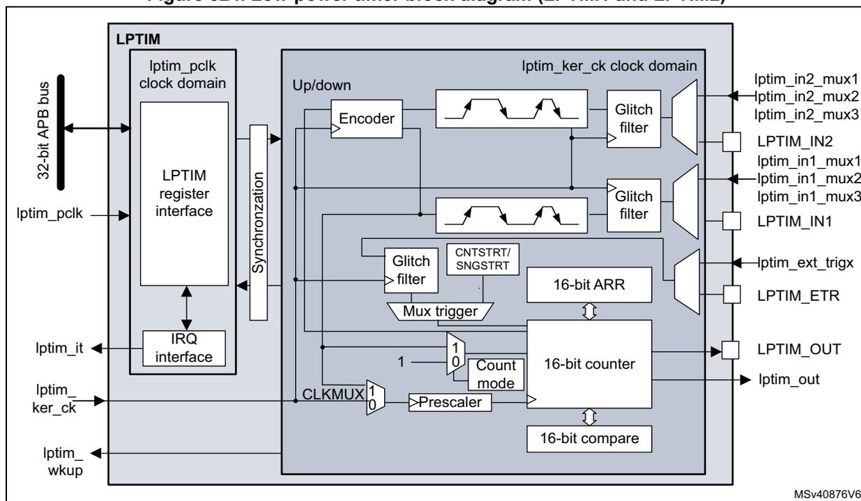
The block diagram illustrates the internal architecture of the Low-Power Timer (LPTIM) for LPTIM1 and LPTIM2. On the left, external connections include a 32-bit APB bus, lptim_pclk , lptim_it , lptim_ker_ck , and lptim_wkup . The lptim_pclk domain contains the LPTIM register interface and the IRQ interface. A synchronization block connects the register interface to the internal logic. The lptim_ker_ck clock domain contains the core timer logic: an Up/down counter, an Encoder, Glitch filters, a Mux trigger, a 16-bit ARR (Auto-Reload Register), a 16-bit counter, and a 16-bit compare unit. The counter is controlled by a CLKMUX (selecting between lptim_ker_ck and lptim_wkup ) and a Prescaler. The Mux trigger is connected to the CNTSTRT/SNGSTRT input. On the right, external pins are labeled lptim_in2_mux1 , lptim_in2_mux2 , lptim_in2_mux3 , LPTIM_IN2 , lptim_in1_mux1 , lptim_in1_mux2 , lptim_in1_mux3 , LPTIM_IN1 , lptim_ext_trigx , LPTIM_ETR , LPTIM_OUT , and lptim_out . The diagram is labeled MSv40876V6.
Figure 525. Low-power timer block diagram (LPTIM3)
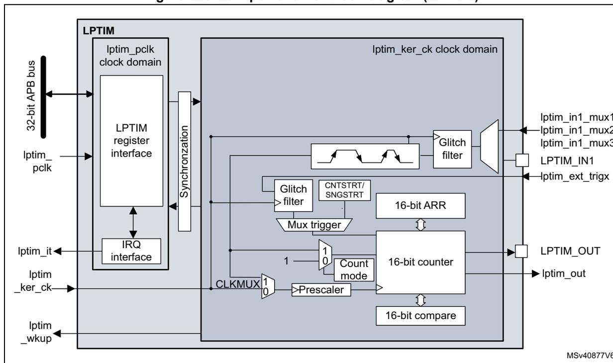
This block diagram illustrates the internal architecture of LPTIM3. On the left, external signals include a 32-bit APB bus, Iptim_pclk, Iptim_it, Iptim_ker_ck, and Iptim_wkup. The Iptim_pclk connects to the LPTIM register interface. The Iptim_ker_ck signal enters the 'lptim_ker_ck clock domain' through a CLKMUX (selecting between 1 and 0). The Iptim_wkup signal connects to the IRQ interface. The LPTIM register interface is connected to the 32-bit APB bus and the Synchronization block. The Synchronization block connects to the Glitch filter and the Mux trigger. The Glitch filter is connected to the CNTSTRT/SNGSTRT signal. The Mux trigger is connected to the 16-bit ARR and the 16-bit counter. The 16-bit ARR is connected to the 16-bit counter. The 16-bit counter is connected to the 16-bit compare and the Lptim_out signal. The 16-bit compare is connected to the 16-bit counter. The Lptim_out signal is also connected to the Glitch filter. The Glitch filter is connected to the Iptim_in1_mux1, Iptim_in1_mux2, and Iptim_in1_mux3 signals. The Iptim_IN1 signal is connected to the Glitch filter. The Iptim_ext_trigx signal is connected to the Glitch filter. The MSV40877V6 identifier is present in the bottom right corner.
Figure 526. Low-power timer block diagram (LPTIM4 and LPTIM5)
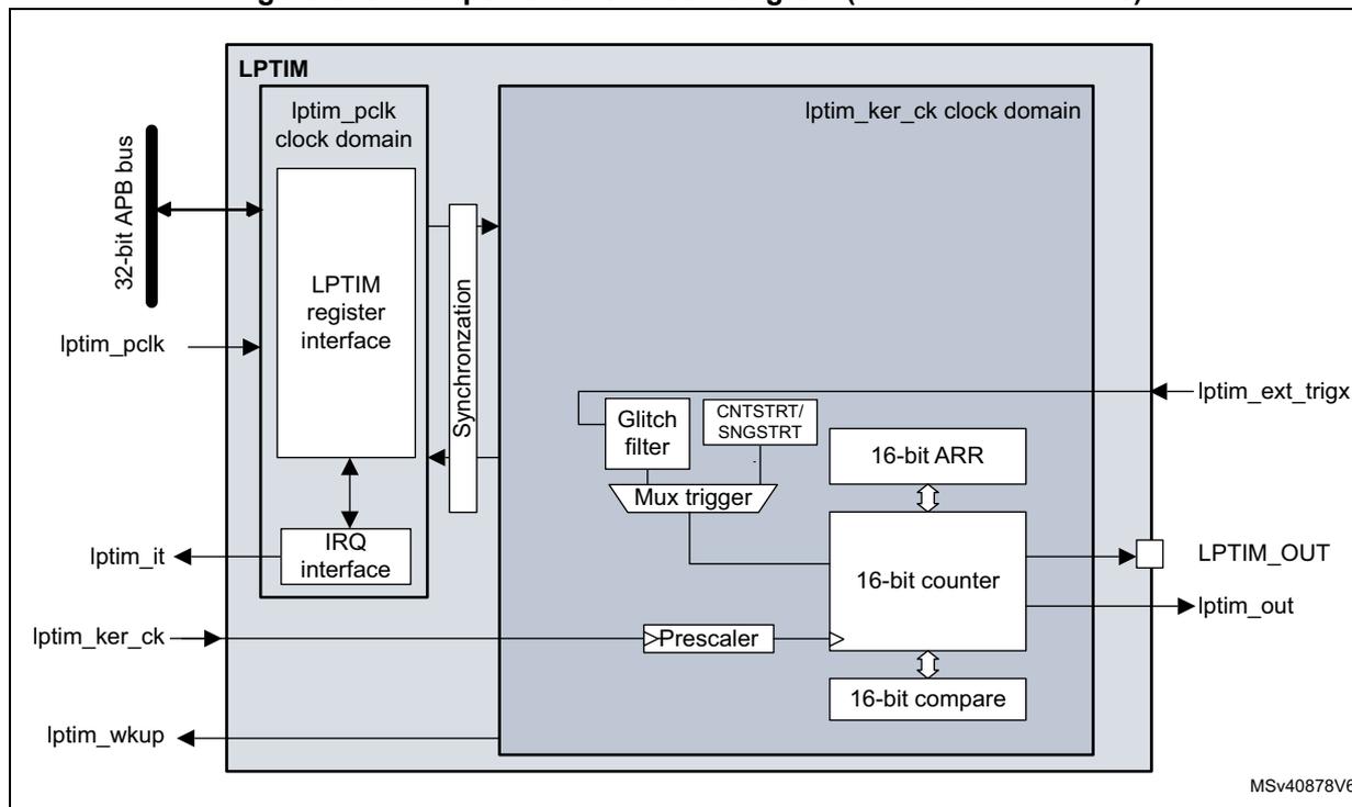
This block diagram illustrates the internal architecture of LPTIM4 and LPTIM5. On the left, external signals include a 32-bit APB bus, Iptim_pclk, Iptim_it, Iptim_ker_ck, and Iptim_wkup. The Iptim_pclk connects to the LPTIM register interface. The Iptim_ker_ck signal enters the 'lptim_ker_ck clock domain' through a Prescaler. The Iptim_wkup signal connects to the IRQ interface. The LPTIM register interface is connected to the 32-bit APB bus and the Synchronization block. The Synchronization block connects to the Glitch filter and the Mux trigger. The Glitch filter is connected to the CNTSTRT/SNGSTRT signal. The Mux trigger is connected to the 16-bit ARR and the 16-bit counter. The 16-bit ARR is connected to the 16-bit counter. The 16-bit counter is connected to the 16-bit compare and the Lptim_out signal. The 16-bit compare is connected to the 16-bit counter. The Lptim_out signal is also connected to the Glitch filter. The Iptim_ext_trigx signal is connected to the Glitch filter. The MSV40877V6 identifier is present in the bottom right corner.
43.4.2 LPTIM pins and internal signals
The following tables provide the list of LPTIM pins and internal signals, respectively.
Table 353. LPTIM input/output pins
| Names | Signal type | Description |
|---|---|---|
| LPTIM_IN1 | Digital input | LPTIM Input 1 from GPIO pin on mux input 0 |
| LPTIM_IN2 | Digital input | LPTIM Input 2 from GPIO pin on mux input 0 |
| LPTIM_ETR | Digital input | LPTIM external trigger GPIO pin |
| LPTIM_OUT | Digital output | LPTIM Output GPIO pin |
Table 354. LPTIM internal signals
| Names | Signal type | Description |
|---|---|---|
| lptim_pclk | Digital input | LPTIM APB clock domain |
| lptim_ker_ck | Digital input | LPTIM kernel clock |
| lptim_in1_mux1 | Digital input | Internal LPTIM input 1 connected to mux input 1 |
| lptim_in1_mux2 | Digital input | Internal LPTIM input 1 connected to mux input 2 |
| lptim_in1_mux3 | Digital input | Internal LPTIM input 1 connected to mux input 3 |
| lptim_in2_mux1 | Digital input | Internal LPTIM input 2 connected to mux input 1 |
| lptim_in2_mux2 | Digital input | Internal LPTIM input 2 connected to mux input 2 |
| lptim_in2_mux3 | Digital input | Internal LPTIM input 2 connected to mux input 3 |
| lptim_ext_trigx | Digital input | LPTIM external trigger input x |
| lptim_out | Digital output | LPTIM counter output |
| lptim_it | Digital output | LPTIM global interrupt |
| lptim_wakeup | Digital output | LPTIM wakeup event |
43.4.3 LPTIM input and trigger mapping
The LPTIM external trigger and input connections are detailed hereafter:
Table 355. LPTIM1 external trigger connection
| TRIGSEL | External trigger |
|---|---|
| lptim_ext_trig0 | GPIO pin as LPTIM1_ETR alternate function |
| lptim_ext_trig1 | RTC_ALARM_A |
| lptim_ext_trig2 | RTC_ALARM_B |
| lptim_ext_trig3 | RTC_TAMP1_OUT |
| lptim_ext_trig4 | RTC_TAMP2_OUT |
| lptim_ext_trig5 | RTC_TAMP3_OUT |
| TRIGSEL | External trigger |
|---|---|
| lptim_ext_trig6 | COMP1_OUT |
| lptim_ext_trig7 | COMP2_OUT |
| TRIGSEL | External trigger |
|---|---|
| lptim_ext_trig0 | GPIO pin as LPTIM2_ETR alternate function |
| lptim_ext_trig1 | RTC_ALARM_A |
| lptim_ext_trig2 | RTC_ALARM_B |
| lptim_ext_trig3 | RTC_TAMP1_OUT |
| lptim_ext_trig4 | RTC_TAMP2_OUT |
| lptim_ext_trig5 | RTC_TAMP3_OUT |
| lptim_ext_trig6 | COMP1_OUT |
| lptim_ext_trig7 | COMP2_OUT |
| TRIGSEL | External trigger |
|---|---|
| lptim_ext_trig0 | LPTIM2_OUT |
| lptim_ext_trig1 | Not connected |
| lptim_ext_trig2 | LPTIM4_OUT |
| lptim_ext_trig3 | LPTIM5_OUT |
| lptim_ext_trig4 | SAI1_FS_A |
| lptim_ext_trig5 | SAI1_FS_B |
| lptim_ext_trig6 | Not connected |
| lptim_ext_trig7 | Not connected |
| TRIGSEL | External trigger |
|---|---|
| lptim_ext_trig0 | LPTIM2_OUT |
| lptim_ext_trig1 | LPTIM3_OUT |
| lptim_ext_trig2 | Not connected |
| lptim_ext_trig3 | LPTIM5_OUT |
| lptim_ext_trig4 | SAI2_FS_A |
| lptim_ext_trig5 | SAI2_FS_B |
| TRIGSEL | External trigger |
|---|---|
| lptim_ext_trig6 | Not connected |
| lptim_ext_trig7 | Not connected |
| TRIGSEL | External trigger |
|---|---|
| lptim_ext_trig0 | LPTIM2_OUT |
| lptim_ext_trig1 | LPTIM3_OUT |
| lptim_ext_trig2 | LPTIM4_OUT |
| lptim_ext_trig3 | SAI4_FS_A |
| lptim_ext_trig4 | SAI4_FS_B |
| lptim_ext_trig5 | Not connected |
| lptim_ext_trig6 | Not connected |
| lptim_ext_trig7 | Not connected |
| lptim_in1_mux | LPTIM1 input 1 connected to |
|---|---|
| lptim_in1_mux0 | GPIO pin as LPTIM1_IN1 alternate function |
| lptim_in1_mux1 | COMP1_OUT |
| lptim_in1_mux2 | Not connected |
| lptim_in1_mux3 | Not connected |
| lptim_in2_mux | LPTIM1 input 2 connected to |
|---|---|
| lptim_in2_mux0 | GPIO pin as LPTIM1_IN2 alternate function |
| lptim_in2_mux1 | COMP2_OUT |
| lptim_in2_mux2 | Not connected |
| lptim_in2_mux3 | Not connected |
| lptim_in1_mux | LPTIM2 input 1 connected to |
|---|---|
| lptim_in1_mux0 | GPIO pin as LPTIM2_IN1 alternate function |
| lptim_in1_mux1 | COMP1_OUT |
| lptim_in1_mux2 | COMP2_OUT |
| lptim_in1_mux3 | COMP1_OUT OR COMP2_OUT |
| lptim_in2_mux | LPTIM2 input 2 connected to |
|---|---|
| lptim_in2_mux0 | GPIO pin as LPTIM2_IN2 alternate function |
| lptim_in2_mux1 | COMP2_OUT |
| lptim_in2_mux2 | Not connected |
| lptim_in2_mux3 | Not connected |
| lptim_in1_mux | LPTIM3 Input 1 connected to |
|---|---|
| lptim_in1_mux0 | Not connected |
| lptim_in1_mux1 | SAI4_FS_A |
| lptim_in1_mux2 | SAI4_FS_B |
| lptim_in1_mux3 | Not connected |
43.4.4 LPTIM reset and clocks
The LPTIM can be clocked using several clock sources. It can be clocked using an internal clock signal which can be any configurable internal clock source selectable through the RCC (see RCC section for more details). Also, the LPTIM can be clocked using an external clock signal injected on its external Input1. When clocked with an external clock source, the LPTIM may run in one of these two possible configurations:
- • The first configuration is when the LPTIM is clocked by an external signal but in the same time an internal clock signal is provided to the LPTIM from configurable internal clock source (see RCC section).
- • The second configuration is when the LPTIM is solely clocked by an external clock source through its external Input1. This configuration is the one used to realize Timeout function or Pulse counter function when all the embedded oscillators are turned off after entering a low-power mode.
Programming the CKSEL and COUNTMODE bits allows controlling whether the LPTIM will use an external clock source or an internal one.
When configured to use an external clock source, the CKPOL bits are used to select the external clock signal active edge. If both edges are configured to be active ones, an internal clock signal should also be provided (first configuration). In this case, the internal clock signal frequency should be at least four times higher than the external clock signal frequency.
43.4.5 Glitch filter
The LPTIM inputs, either external (mapped to GPIOs) or internal (mapped on the chip-level to other embedded peripherals), are protected with digital filters that prevent any glitches and noise perturbations to propagate inside the LPTIM. This is in order to prevent spurious counts or triggers.
Before activating the digital filters, an internal clock source should first be provided to the LPTIM. This is necessary to guarantee the proper operation of the filters.
The digital filters are divided into two groups:
- • The first group of digital filters protects the LPTIM external inputs. The digital filters sensitivity is controlled by the CKFLT bits
- • The second group of digital filters protects the LPTIM internal trigger inputs. The digital filters sensitivity is controlled by the TRGFLT bits.
Note: The digital filters sensitivity is controlled by groups. It is not possible to configure each digital filter sensitivity separately inside the same group.
The filter sensitivity acts on the number of consecutive equal samples that should be detected on one of the LPTIM inputs to consider a signal level change as a valid transition. Figure 527 shows an example of glitch filter behavior in case of a 2 consecutive samples programmed.
Figure 527. Glitch filter timing diagram
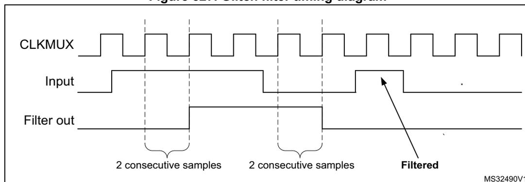
The diagram illustrates the glitch filter's operation. The top waveform, CLKMUX, is a periodic square wave representing the clock. The middle waveform, Input, shows a signal that transitions from high to low and back to high. A short pulse (glitch) is visible. The bottom waveform, Filter out, shows the output of the filter. The filter output remains high until after the glitch has passed, then it transitions to low. Vertical dashed lines mark the sampling points. Brackets below the Input signal indicate '2 consecutive samples' where the signal was low. An arrow points to the Filter out signal with the label 'Filtered'. The diagram is labeled MS32490V1 in the bottom right corner.
Note: In case no internal clock signal is provided, the digital filter must be deactivated by setting the CKFLT and TRGFLT bits to '0'. In that case, an external analog filter may be used to protect the LPTIM external inputs against glitches.
43.4.6 Prescaler
The LPTIM 16-bit counter is preceded by a configurable power-of-2 prescaler. The prescaler division ratio is controlled by the PRESC[2:0] 3-bit field. The table below lists all the possible division ratios:
Table 365. Prescaler division ratios
| programming | dividing factor |
|---|---|
| 000 | /1 |
| 001 | /2 |
| 010 | /4 |
| 011 | /8 |
| 100 | /16 |
| 101 | /32 |
| 110 | /64 |
| 111 | /128 |
43.4.7 Trigger multiplexer
The LPTIM counter may be started either by software or after the detection of an active edge on one of the 8 trigger inputs.
TRIGEN[1:0] is used to determine the LPTIM trigger source:
- • When TRIGEN[1:0] equals '00', The LPTIM counter is started as soon as one of the CNTSTRT or the SNGSTRT bits is set by software. The three remaining possible values for the TRIGEN[1:0] are used to configure the active edge used by the trigger inputs. The LPTIM counter starts as soon as an active edge is detected.
- • When TRIGEN[1:0] is different than '00', TRIGSEL[2:0] is used to select which of the 8 trigger inputs is used to start the counter.
The external triggers are considered asynchronous signals for the LPTIM. So after a trigger detection, a two-counter-clock period latency is needed before the timer starts running due to the synchronization.
If a new trigger event occurs when the timer is already started it will be ignored (unless timeout function is enabled).
Note: The timer must be enabled before setting the SNGSTRT/CNTSTRT bits. Any write on these bits when the timer is disabled will be discarded by hardware.
Note: When starting the counter by software (TRIGEN[1:0] = 00), there is a delay of 3 kernel clock cycles between the LPTIM_CR register update (set one of SNGSTRT or CNTSTRT bits) and the effective start of the counter.
43.4.8 Operating mode
The LPTIM features two operating modes:
- • The Continuous mode: the timer is free running, the timer is started from a trigger event and never stops until the timer is disabled
- • One-shot mode: the timer is started from a trigger event and stops when reaching the ARR value.
One-shot mode
To enable the one-shot counting, the SNGSTRT bit must be set.
A new trigger event will re-start the timer. Any trigger event occurring after the counter starts and before the counter reaches ARR will be discarded.
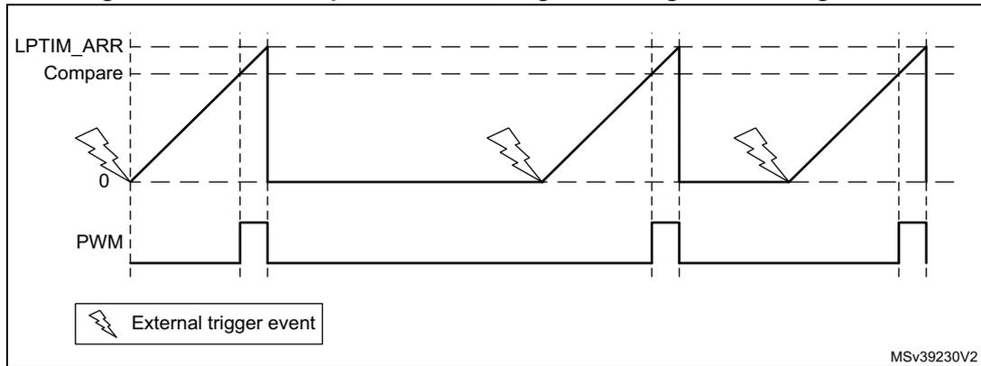
In case an external trigger is selected, each external trigger event arriving after the SNGSTRT bit is set, and after the counter register has stopped (contains zero value), will start the counter for a new one-shot counting cycle as shown in Figure 528 .
Figure 528. LPTIM output waveform, single counting mode configuration
Set-once mode activated:
It should be noted that when the WAVE bit-field in the LPTIM_CFGR register is set, the Set-once mode is activated. In this case, the counter is only started once following the first trigger, and any subsequent trigger event is discarded as shown in Figure 529.
Figure 529. LPTIM output waveform, Single counting mode configuration and Set-once mode activated (WAVE bit is set)
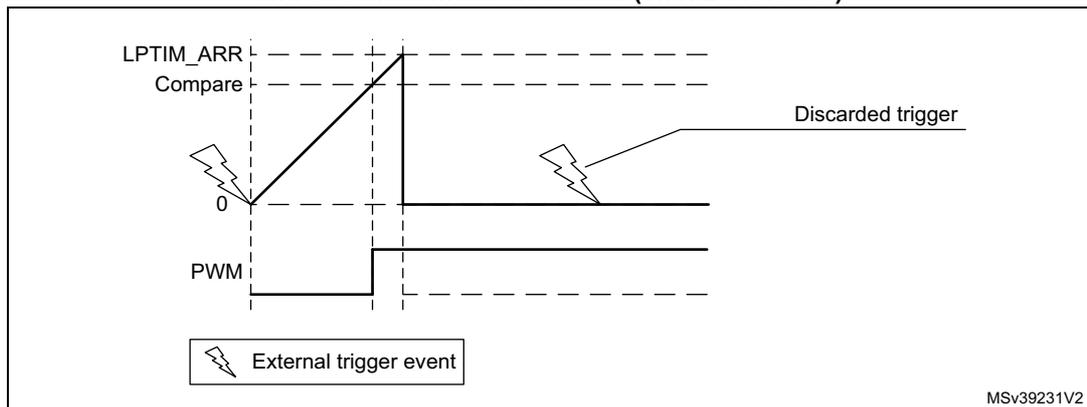
In case of software start (TRIGEN[1:0] = '00'), the SNGSTRT setting will start the counter for one-shot counting.
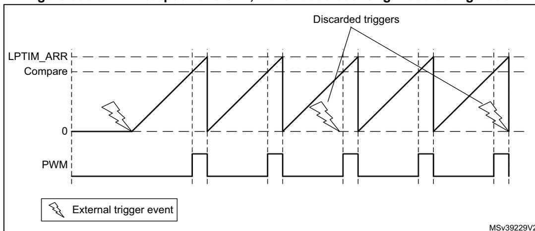
Continuous mode
To enable the continuous counting, the CNTSTRT bit must be set.
In case an external trigger is selected, an external trigger event arriving after CNTSTRT is set will start the counter for continuous counting. Any subsequent external trigger event will be discarded as shown in Figure 530.
In case of software start (TRIGEN[1:0] = '00'), setting CNTSTRT will start the counter for continuous counting.
Figure 530. LPTIM output waveform, Continuous counting mode configuration
SNGSTRT and CNTSTRT bits can only be set when the timer is enabled (The ENABLE bit is set to '1'). It is possible to change "on the fly" from One-shot mode to Continuous mode.
If the Continuous mode was previously selected, setting SNGSTRT will switch the LPTIM to the One-shot mode. The counter (if active) will stop as soon as it reaches ARR.
If the One-shot mode was previously selected, setting CNTSTRT will switch the LPTIM to the Continuous mode. The counter (if active) will restart as soon as it reaches ARR.
43.4.9 Timeout function
The detection of an active edge on one selected trigger input can be used to reset the LPTIM counter. This feature is controlled through the TIMEOUT bit.
The first trigger event will start the timer, any successive trigger event will reset the counter and the timer will restart.
A low-power timeout function can be realized. The timeout value corresponds to the compare value; if no trigger occurs within the expected time frame, the MCU is waked-up by the compare match event.
43.4.10 Waveform generation
Two 16-bit registers, the LPTIM_ARR (autoreload register) and LPTIM_CMP (compare register), are used to generate several different waveforms on LPTIM output
The timer can generate the following waveforms:
- • The PWM mode: the LPTIM output is set as soon as the counter value in LPTIM_CNT exceeds the compare value in LPTIM_CMP. The LPTIM output is reset as soon as a match occurs between the LPTIM_ARR and the LPTIM_CNT registers.
- • The One-pulse mode: the output waveform is similar to the one of the PWM mode for the first pulse, then the output is permanently reset
- • The Set-once mode: the output waveform is similar to the One-pulse mode except that the output is kept to the last signal level (depends on the output configured polarity).
The above described modes require that the LPTIM_ARR register value be strictly greater than the LPTIM_CMP register value.
The LPTIM output waveform can be configured through the WAVE bit as follow:
- • Resetting the WAVE bit to '0' forces the LPTIM to generate either a PWM waveform or a One pulse waveform depending on which bit is set: CNTSTRT or SNGSTRT.
- • Setting the WAVE bit to '1' forces the LPTIM to generate a Set-once mode waveform.
The WAVPOL bit controls the LPTIM output polarity. The change takes effect immediately, so the output default value will change immediately after the polarity is re-configured, even before the timer is enabled.
Signals with frequencies up to the LPTIM clock frequency divided by 2 can be generated.
Figure 531 below shows the three possible waveforms that can be generated on the LPTIM output. Also, it shows the effect of the polarity change using the WAVPOL bit.
Figure 531. Waveform generation
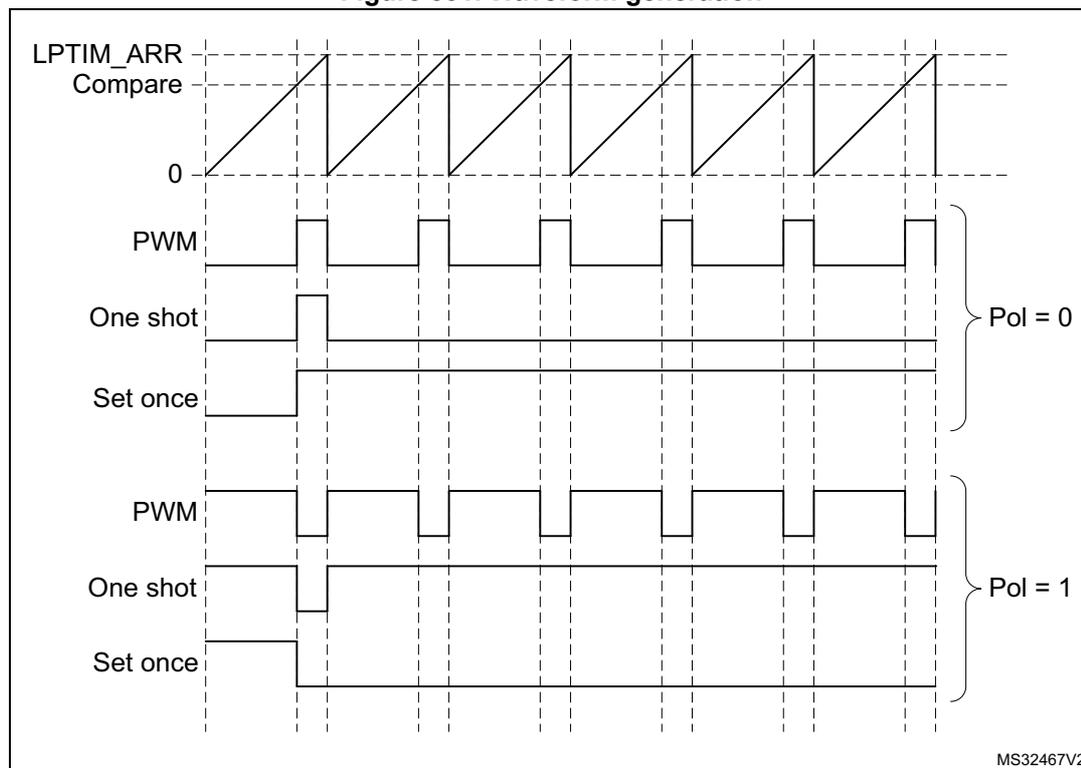
The figure is a timing diagram illustrating the output waveforms of an LPTIM. At the top, the LPTIM_ARR register value is shown as a sawtooth waveform, starting at 0 and increasing linearly until it reaches the ARR value, then resetting to 0. Below this, the Compare register value is shown as a horizontal dashed line. The output waveforms are shown for two polarity settings: Pol = 0 and Pol = 1. For Pol = 0, the PWM output is a periodic square wave, the One shot output is a single pulse, and the Set once output is a single pulse. For Pol = 1, the PWM output is the inverted PWM, the One shot output is an inverted single pulse, and the Set once output is an inverted single pulse. The diagram is labeled MS32467V2 in the bottom right corner.
43.4.11 Register update
The LPTIM_ARR register and LPTIM_CMP register are updated immediately after the APB bus write operation, or at the end of the current period if the timer is already started.
The PRELOAD bit controls how the LPTIM_ARR and the LPTIM_CMP registers are updated:
- • When the PRELOAD bit is reset to '0', the LPTIM_ARR and the LPTIM_CMP registers are immediately updated after any write access.
- • When the PRELOAD bit is set to '1', the LPTIM_ARR and the LPTIM_CMP registers are updated at the end of the current period, if the timer has been already started.
The LPTIM APB interface and the LPTIM kernel logic use different clocks, so there is some latency between the APB write and the moment when these values are available to the
counter comparator. Within this latency period, any additional write into these registers must be avoided.
The ARROK flag and the CMPOK flag in the LPTIM_ISR register indicate when the write operation is completed to respectively the LPTIM_ARR register and the LPTIM_CMP register.
After a write to the LPTIM_ARR register or the LPTIM_CMP register, a new write operation to the same register can only be performed when the previous write operation is completed. Any successive write before respectively the ARROK flag or the CMPOK flag be set, will lead to unpredictable results.
43.4.12 Counter mode
The LPTIM counter can be used to count external events on the LPTIM Input1 or it can be used to count internal clock cycles. The CKSEL and COUNTMODE bits control which source will be used for updating the counter.
In case the LPTIM is configured to count external events on Input1, the counter can be updated following a rising edge, falling edge or both edges depending on the value written to the CKPOL[1:0] bits.
The count modes below can be selected, depending on CKSEL and COUNTMODE values:
- • CKSEL = 0: the LPTIM is clocked by an internal clock source
- – COUNTMODE = 0
The LPTIM is configured to be clocked by an internal clock source and the LPTIM counter is configured to be updated following each internal clock pulse. - – COUNTMODE = 1
The LPTIM external Input1 is sampled with the internal clock provided to the LPTIM.
Consequently, in order not to miss any event, the frequency of the changes on the external Input1 signal should never exceed the frequency of the internal clock provided to the LPTIM. Also, the internal clock provided to the LPTIM must not be prescaled (PRESC[2:0] = 000).
- – COUNTMODE = 0
- • CKSEL = 1: the LPTIM is clocked by an external clock source
COUNTMODE value is don't care.
In this configuration, the LPTIM has no need for an internal clock source (except if the glitch filters are enabled). The signal injected on the LPTIM external Input1 is used as system clock for the LPTIM. This configuration is suitable for operation modes where no embedded oscillator is enabled.
For this configuration, the LPTIM counter can be updated either on rising edges or falling edges of the input1 clock signal but not on both rising and falling edges.
Since the signal injected on the LPTIM external Input1 is also used to clock the LPTIM kernel logic, there is some initial latency (after the LPTIM is enabled) before the counter is incremented. More precisely, the first five active edges on the LPTIM external Input1 (after LPTIM is enable) are lost.
43.4.13 Timer enable
The ENABLE bit located in the LPTIM_CR register is used to enable/disable the LPTIM kernel logic. After setting the ENABLE bit, a delay of two counter clock is needed before the LPTIM is actually enabled.
The LPTIM_CFGR and LPTIM_IER registers must be modified only when the LPTIM is disabled.
43.4.14 Timer counter reset
In order to reset the content of LPTIM_CNT register to zero, two reset mechanisms are implemented:
- • The synchronous reset mechanism: the synchronous reset is controlled by the COUNTRST bit in the LPTIM_CR register. After setting the COUNTRST bit-field to '1', the reset signal is propagated in the LPTIM kernel clock domain. So it is important to note that a few clock pulses of the LPTIM kernel logic will elapse before the reset is taken into account. This will make the LPTIM counter count few extra pluses between the time when the reset is trigger and it become effective. Since the COUNTRST bit is located in the APB clock domain and the LPTIM counter is located in the LPTIM kernel clock domain, a delay of 3 clock cycles of the kernel clock is needed to synchronize the reset signal issued by the APB clock domain when writing '1' to the COUNTRST bit.
- • The asynchronous reset mechanism: the asynchronous reset is controlled by the RSTARE bit located in the LPTIM_CR register. When this bit is set to '1', any read access to the LPTIM_CNT register will reset its content to zero. Asynchronous reset should be triggered within a timeframe in which no LPTIM core clock is provided. For example when LPTIM Input1 is used as external clock source, the asynchronous reset should be applied only when there is enough insurance that no toggle will occur on the LPTIM Input1.
It should be noted that to read reliably the content of the LPTIM_CNT register two successive read accesses must be performed and compared. A read access can be considered reliable when the value of the two read accesses is equal. Unfortunately when asynchronous reset is enabled there is no possibility to read twice the LPTIM_CNT register.
Warning: There is no mechanism inside the LPTIM that prevents the two reset mechanisms from being used simultaneously. So developer should make sure that these two mechanisms are used exclusively.
43.4.15 Encoder mode
This mode allows handling signals from quadrature encoders used to detect angular position of rotary elements. Encoder interface mode acts simply as an external clock with direction selection. This means that the counter just counts continuously between 0 and the auto-reload value programmed into the LPTIM_ARR register (0 up to ARR or ARR down to 0 depending on the direction). Therefore LPTIM_ARR must be configured before starting the counter. From the two external input signals, Input1 and Input2, a clock signal is generated to clock the LPTIM counter. The phase between those two signals determines the counting direction.
The Encoder mode is only available when the LPTIM is clocked by an internal clock source. The signals frequency on both Input1 and Input2 inputs must not exceed the LPTIM internal clock frequency divided by 4. This is mandatory in order to guarantee a proper operation of the LPTIM.
Direction change is signaled by the two Down and Up flags in the LPTIM_ISR register. Also, an interrupt can be generated for both direction change events if enabled through the DOWNIE bit.
To activate the Encoder mode the ENC bit has to be set to '1'. The LPTIM must first be configured in Continuous mode.
When Encoder mode is active, the LPTIM counter is modified automatically following the speed and the direction of the incremental encoder. Therefore, its content always represents the encoder's position. The count direction, signaled by the Up and Down flags, correspond to the rotation direction of the encoder rotor.
According to the edge sensitivity configured using the CKPOL[1:0] bits, different counting scenarios are possible. The following table summarizes the possible combinations, assuming that Input1 and Input2 do not switch at the same time.
Table 366. Encoder counting scenarios
| Active edge | Level on opposite signal (Input1 for Input2, Input2 for Input1) | Input1 signal | Input2 signal | ||
|---|---|---|---|---|---|
| Rising | Falling | Rising | Falling | ||
| Rising Edge | High | Down | No count | Up | No count |
| Low | Up | No count | Down | No count | |
| Falling Edge | High | No count | Up | No count | Down |
| Low | No count | Down | No count | Up | |
| Both Edges | High | Down | Up | Up | Down |
| Low | Up | Down | Down | Up | |
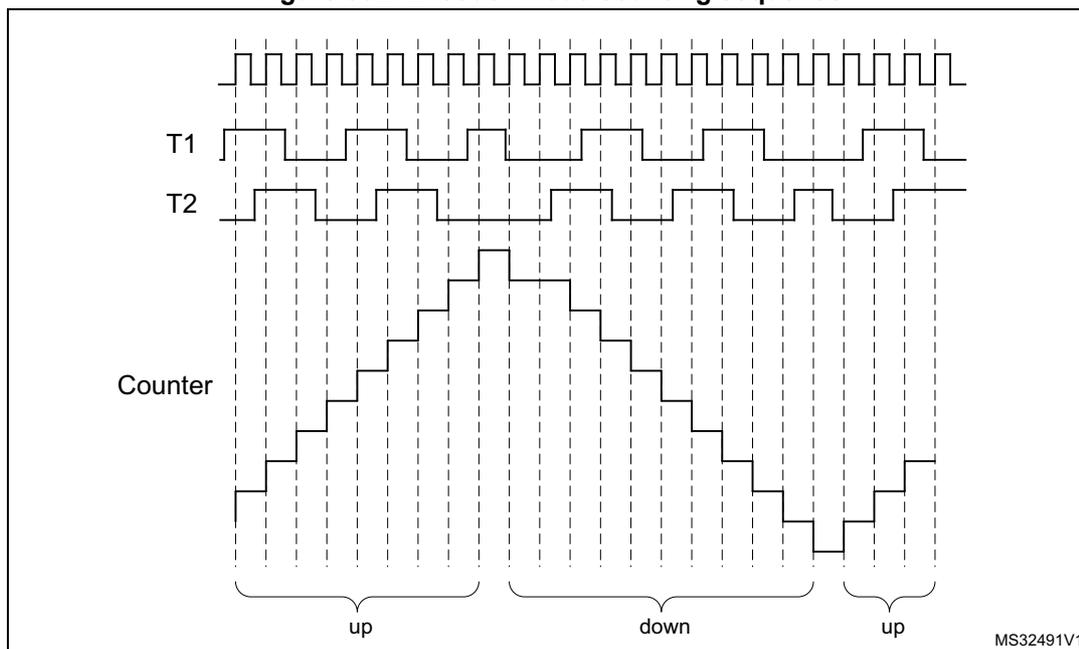
The following figure shows a counting sequence for Encoder mode where both-edge sensitivity is configured.
Caution: In this mode the LPTIM must be clocked by an internal clock source, so the CKSEL bit must be maintained to its reset value which is equal to '0'. Also, the prescaler division ratio must be equal to its reset value which is 1 (PRESC[2:0] bits must be '000').
Figure 532. Encoder mode counting sequence
43.4.16 Debug mode
When the microcontroller enters debug mode (core halted), the LPTIM counter either continues to work normally or stops, depending on the DBG_LPTIM_STOP configuration bit in the DBG module.
43.5 LPTIM low-power modes
Table 367. Effect of low-power modes on the LPTIM
| Mode | Description |
|---|---|
| Sleep | No effect. LPTIM interrupts cause the device to exit Sleep mode. |
| Stop | The LPTIM peripheral is active when it is clocked by LSE or LSI. LPTIM interrupts cause the device to exit Stop mode |
| Standby | The LPTIM peripheral is powered down and must be reinitialized after exiting Standby mode. |
43.6 LPTIM interrupts
The following events generate an interrupt/wake-up event, if they are enabled through the LPTIM_IER register:
- • Compare match
- • Auto-reload match (whatever the direction if encoder mode)
- • External trigger event
- • Autoreload register write completed
- • Compare register write completed
- • Direction change (encoder mode), programmable (up / down / both).
Note: If any bit in the LPTIM_IER register (Interrupt Enable Register) is set after that its corresponding flag in the LPTIM_ISR register (Status Register) is set, the interrupt is not asserted.
Table 368. Interrupt events
| Interrupt event | Description |
|---|---|
| Compare match | Interrupt flag is raised when the content of the Counter register (LPTIM_CNT) matches the content of the compare register (LPTIM_CMP). |
| Auto-reload match | Interrupt flag is raised when the content of the Counter register (LPTIM_CNT) matches the content of the Auto-reload register (LPTIM_ARR). |
| External trigger event | Interrupt flag is raised when an external trigger event is detected |
| Auto-reload register update OK | Interrupt flag is raised when the write operation to the LPTIM_ARR register is complete. |
| Compare register update OK | Interrupt flag is raised when the write operation to the LPTIM_CMP register is complete. |
| Direction change | Used in Encoder mode. Two interrupt flags are embedded to signal direction change:
|
43.7 LPTIM registers
Refer to Section 1.2: List of abbreviations for registers for a list of abbreviations used in register descriptions.
The peripheral registers can only be accessed by words (32-bit).
43.7.1 LPTIM interrupt and status register (LPTIM_ISR)
Address offset: 0x000
Reset value: 0x0000 0000
| 31 | 30 | 29 | 28 | 27 | 26 | 25 | 24 | 23 | 22 | 21 | 20 | 19 | 18 | 17 | 16 |
|---|---|---|---|---|---|---|---|---|---|---|---|---|---|---|---|
| Res. | Res. | Res. | Res. | Res. | Res. | Res. | Res. | Res. | Res. | Res. | Res. | Res. | Res. | Res. | Res. |
| 15 | 14 | 13 | 12 | 11 | 10 | 9 | 8 | 7 | 6 | 5 | 4 | 3 | 2 | 1 | 0 |
| Res. | Res. | Res. | Res. | Res. | Res. | Res. | Res. | Res. | DOWN | UP | ARR OK | CMP OK | EXT TRIG | ARRM | CMPM |
| r | r | r | r | r | r | r |
Bits 31:7 Reserved, must be kept at reset value.
Bit 6 DOWN : Counter direction change up to down
In Encoder mode, DOWN bit is set by hardware to inform application that the counter direction has changed from up to down. DOWN flag can be cleared by writing 1 to the DOWNCF bit in the LPTIM_ICR register.
Note: If the LPTIM does not support encoder mode feature, this bit is reserved. Please refer to Section 43.3: LPTIM implementation .
Bit 5 UP : Counter direction change down to up
In Encoder mode, UP bit is set by hardware to inform application that the counter direction has changed from down to up. UP flag can be cleared by writing 1 to the UP CF bit in the LPTIM_ICR register.
Note: If the LPTIM does not support encoder mode feature, this bit is reserved. Please refer to Section 43.3: LPTIM implementation .
Bit 4 ARROK : Autoreload register update OK
ARROK is set by hardware to inform application that the APB bus write operation to the LPTIM_ARR register has been successfully completed. ARROK flag can be cleared by writing 1 to the ARROKCF bit in the LPTIM_ICR register.
Bit 3 CMPOK : Compare register update OK
CMPOK is set by hardware to inform application that the APB bus write operation to the LPTIM_CMP register has been successfully completed. CMPOK flag can be cleared by writing 1 to the CMPOKCF bit in the LPTIM_ICR register.
Bit 2 EXTTRIG : External trigger edge event
EXTTRIG is set by hardware to inform application that a valid edge on the selected external trigger input has occurred. If the trigger is ignored because the timer has already started, then this flag is not set. EXTTRIG flag can be cleared by writing 1 to the EXTTRIGCF bit in the LPTIM_ICR register.
Bit 1 ARRM : Autoreload match
ARRM is set by hardware to inform application that LPTIM_CNT register's value reached the LPTIM_ARR register's value. ARRM flag can be cleared by writing 1 to the ARRMCF bit in the LPTIM_ICR register.
Bit 0 CMPM : Compare match
The CMPM bit is set by hardware to inform application that LPTIM_CNT register value reached the LPTIM_CMP register's value. CMPM flag can be cleared by writing 1 to the CMPMCF bit in the LPTIM_ICR register.
43.7.2 LPTIM interrupt clear register (LPTIM_ICR)
Address offset: 0x004
Reset value: 0x0000 0000
| 31 | 30 | 29 | 28 | 27 | 26 | 25 | 24 | 23 | 22 | 21 | 20 | 19 | 18 | 17 | 16 |
|---|---|---|---|---|---|---|---|---|---|---|---|---|---|---|---|
| Res. | Res. | Res. | Res. | Res. | Res. | Res. | Res. | Res. | Res. | Res. | Res. | Res. | Res. | Res. | Res. |
| 15 | 14 | 13 | 12 | 11 | 10 | 9 | 8 | 7 | 6 | 5 | 4 | 3 | 2 | 1 | 0 |
| Res. | Res. | Res. | Res. | Res. | Res. | Res. | Res. | Res. | DOWNCF | UPCF | ARROKCF | CMPOKCF | EXTTRIGCF | ARRMCF | CMPMCF |
| w | w | w | w | w | w | w |
Bits 31:7 Reserved, must be kept at reset value.
Bit 6 DOWNCF : Direction change to down clear flag
Writing 1 to this bit clear the DOWN flag in the LPTIM_ISR register.
Note: If the LPTIM does not support encoder mode feature, this bit is reserved. Please refer to Section 43.3: LPTIM implementation .
Bit 5 UPCF : Direction change to UP clear flag
Writing 1 to this bit clear the UP flag in the LPTIM_ISR register.
Note: If the LPTIM does not support encoder mode feature, this bit is reserved. Please refer to Section 43.3: LPTIM implementation .
Bit 4 ARROKCF : Autoreload register update OK clear flag
Writing 1 to this bit clears the ARROK flag in the LPTIM_ISR register
Bit 3 CMPOKCF : Compare register update OK clear flag
Writing 1 to this bit clears the CMPOK flag in the LPTIM_ISR register
Bit 2 EXTTRIGCF : External trigger valid edge clear flag
Writing 1 to this bit clears the EXTTRIG flag in the LPTIM_ISR register
Bit 1 ARRMCF : Autoreload match clear flag
Writing 1 to this bit clears the ARRM flag in the LPTIM_ISR register
Bit 0 CMPMCF : Compare match clear flag
Writing 1 to this bit clears the CMPM flag in the LPTIM_ISR register
43.7.3 LPTIM interrupt enable register (LPTIM_IER)
Address offset: 0x008
Reset value: 0x0000 0000
| 31 | 30 | 29 | 28 | 27 | 26 | 25 | 24 | 23 | 22 | 21 | 20 | 19 | 18 | 17 | 16 |
|---|---|---|---|---|---|---|---|---|---|---|---|---|---|---|---|
| Res. | Res. | Res. | Res. | Res. | Res. | Res. | Res. | Res. | Res. | Res. | Res. | Res. | Res. | Res. | Res. |
| 15 | 14 | 13 | 12 | 11 | 10 | 9 | 8 | 7 | 6 | 5 | 4 | 3 | 2 | 1 | 0 |
| Res. | Res. | Res. | Res. | Res. | Res. | Res. | Res. | Res. | DOWNIE | UPIE | ARROKIE | CMPOKIE | EXTTRIGIE | ARRMIE | CMPMIE |
| rw | rw | rw | rw | rw | rw | rw |
Bits 31:7 Reserved, must be kept at reset value.
Bit 6 DOWNIE : Direction change to down Interrupt Enable
- 0: DOWN interrupt disabled
- 1: DOWN interrupt enabled
Note: If the LPTIM does not support encoder mode feature, this bit is reserved. Please refer to Section 43.3: LPTIM implementation .
Bit 5 UPIE : Direction change to UP Interrupt Enable
- 0: UP interrupt disabled
- 1: UP interrupt enabled
Note: If the LPTIM does not support encoder mode feature, this bit is reserved. Please refer to Section 43.3: LPTIM implementation .
Bit 4 ARROKIE : Autoreload register update OK Interrupt Enable
- 0: ARROK interrupt disabled
- 1: ARROK interrupt enabled
Bit 3 CMPOKIE : Compare register update OK Interrupt Enable
- 0: CMPOK interrupt disabled
- 1: CMPOK interrupt enabled
Bit 2 EXTTRIGIE : External trigger valid edge Interrupt Enable
- 0: EXTTRIG interrupt disabled
- 1: EXTTRIG interrupt enabled
Bit 1 ARRMIE : Autoreload match Interrupt Enable
- 0: ARRM interrupt disabled
- 1: ARRM interrupt enabled
Bit 0 CMPMIE : Compare match Interrupt Enable
- 0: CMPM interrupt disabled
- 1: CMPM interrupt enabled
Caution: The LPTIM_IER register must only be modified when the LPTIM is disabled (ENABLE bit reset to '0')
43.7.4 LPTIM configuration register (LPTIM_CFGR)
Address offset: 0x00C
Reset value: 0x0000 0000
| 31 | 30 | 29 | 28 | 27 | 26 | 25 | 24 | 23 | 22 | 21 | 20 | 19 | 18 | 17 | 16 |
|---|---|---|---|---|---|---|---|---|---|---|---|---|---|---|---|
| Res. | Res. | Res. | Res. | Res. | Res. | Res. | ENC | COUNT MODE | PRELOAD | WAVPOL | WAVE | TIMOUT | TRIGEN[1:0] | Res. | |
| rw | rw | rw | rw | rw | rw | rw | rw | ||||||||
| 15 | 14 | 13 | 12 | 11 | 10 | 9 | 8 | 7 | 6 | 5 | 4 | 3 | 2 | 1 | 0 |
| TRIGSEL[2:0] | Res. | PRESC[2:0] | Res. | TRGFLT[1:0] | Res. | CKFLT[1:0] | CKPOL[1:0] | CKSEL | |||||||
| rw | rw | rw | rw | rw | rw | rw | rw | rw | rw | rw | rw | rw | |||
Bits 31:30 Reserved, must be kept at reset value.
Bit 29 Reserved, must be kept at reset value.
Bits 28:25 Reserved, must be kept at reset value.
Bit 24 ENC : Encoder mode enable
The ENC bit controls the Encoder mode
0: Encoder mode disabled
1: Encoder mode enabled
Note: If the LPTIM does not support encoder mode feature, this bit is reserved. Please refer to Section 43.3: LPTIM implementation .
Bit 23 COUNTMODE : counter mode enabled
The COUNTMODE bit selects which clock source is used by the LPTIM to clock the counter:
0: the counter is incremented following each internal clock pulse
1: the counter is incremented following each valid clock pulse on the LPTIM external Input1
Bit 22 PRELOAD : Registers update mode
The PRELOAD bit controls the LPTIM_ARR and the LPTIM_CMP registers update modality
0: Registers are updated after each APB bus write access
1: Registers are updated at the end of the current LPTIM period
Bit 21 WAVPOL : Waveform shape polarity
The WAVPOL bit controls the output polarity
0: The LPTIM output reflects the compare results between LPTIM_CNT and LPTIM_CMP registers
1: The LPTIM output reflects the inverse of the compare results between LPTIM_CNT and LPTIM_CMP registers
Bit 20 WAVE : Waveform shape
The WAVE bit controls the output shape
0: Deactivate Set-once mode
1: Activate the Set-once mode
Bit 19 TIMOUT : Timeout enable
The TIMOUT bit controls the Timeout feature
0: A trigger event arriving when the timer is already started will be ignored
1: A trigger event arriving when the timer is already started will reset and restart the counter
Bits 18:17 TRIGEN[1:0] : Trigger enable and polarity
The TRIGEN bits controls whether the LPTIM counter is started by an external trigger or not. If the external trigger option is selected, three configurations are possible for the trigger active edge:
00: software trigger (counting start is initiated by software)
01: rising edge is the active edge
10: falling edge is the active edge
11: both edges are active edges
Bit 16 Reserved, must be kept at reset value.
Bits 15:13 TRIGSEL[2:0] : Trigger selectorThe TRIGSEL bits select the trigger source that will serve as a trigger event for the LPTIM among the below 8 available sources:
- 000: lptim_ext_trig0
- 001: lptim_ext_trig1
- 010: lptim_ext_trig2
- 011: lptim_ext_trig3
- 100: lptim_ext_trig4
- 101: lptim_ext_trig5
- 110: lptim_ext_trig6
- 111: lptim_ext_trig7
See Section 43.4.3: LPTIM input and trigger mapping for details.
Bit 12 Reserved, must be kept at reset value.
Bits 11:9 PRESC[2:0] : Clock prescalerThe PRESC bits configure the prescaler division factor. It can be one among the following division factors:
- 000: /1
- 001: /2
- 010: /4
- 011: /8
- 100: /16
- 101: /32
- 110: /64
- 111: /128
Bit 8 Reserved, must be kept at reset value.
Bits 7:6 TRGFLT[1:0] : Configurable digital filter for triggerThe TRGFLT value sets the number of consecutive equal samples that should be detected when a level change occurs on an internal trigger before it is considered as a valid level transition. An internal clock source must be present to use this feature
- 00: any trigger active level change is considered as a valid trigger
- 01: trigger active level change must be stable for at least 2 clock periods before it is considered as valid trigger.
- 10: trigger active level change must be stable for at least 4 clock periods before it is considered as valid trigger.
- 11: trigger active level change must be stable for at least 8 clock periods before it is considered as valid trigger.
Bit 5 Reserved, must be kept at reset value.
Bits 4:3 CKFLT[1:0] : Configurable digital filter for external clockThe CKFLT value sets the number of consecutive equal samples that should be detected when a level change occurs on an external clock signal before it is considered as a valid level transition. An internal clock source must be present to use this feature
00: any external clock signal level change is considered as a valid transition
01: external clock signal level change must be stable for at least 2 clock periods before it is considered as valid transition.
10: external clock signal level change must be stable for at least 4 clock periods before it is considered as valid transition.
11: external clock signal level change must be stable for at least 8 clock periods before it is considered as valid transition.
Bits 2:1 CKPOL[1:0] : Clock polarityIf LPTIM is clocked by an external clock source:
When the LPTIM is clocked by an external clock source, CKPOL bits is used to configure the active edge or edges used by the counter:
00: the rising edge is the active edge used for counting.
If the LPTIM is configured in Encoder mode (ENC bit is set), the encoder sub-mode 1 is active.
01: the falling edge is the active edge used for counting
If the LPTIM is configured in Encoder mode (ENC bit is set), the encoder sub-mode 2 is active.
10: both edges are active edges. When both external clock signal edges are considered active ones, the LPTIM must also be clocked by an internal clock source with a frequency equal to at least four times the external clock frequency.
If the LPTIM is configured in Encoder mode (ENC bit is set), the encoder sub-mode 3 is active.
11: not allowed
Refer to Section 43.4.15: Encoder mode for more details about Encoder mode sub-modes.
Bit 0 CKSEL : Clock selectorThe CKSEL bit selects which clock source the LPTIM will use:
0: LPTIM is clocked by internal clock source (APB clock or any of the embedded oscillators)
1: LPTIM is clocked by an external clock source through the LPTIM external Input1
Caution: The LPTIM_CFGR register must only be modified when the LPTIM is disabled (ENABLE bit reset to '0').
43.7.5 LPTIM control register (LPTIM_CR)
Address offset: 0x010
Reset value: 0x0000 0000
| 31 | 30 | 29 | 28 | 27 | 26 | 25 | 24 | 23 | 22 | 21 | 20 | 19 | 18 | 17 | 16 |
|---|---|---|---|---|---|---|---|---|---|---|---|---|---|---|---|
| Res. | Res. | Res. | Res. | Res. | Res. | Res. | Res. | Res. | Res. | Res. | Res. | Res. | Res. | Res. | Res. |
| 15 | 14 | 13 | 12 | 11 | 10 | 9 | 8 | 7 | 6 | 5 | 4 | 3 | 2 | 1 | 0 |
| Res. | Res. | Res. | Res. | Res. | Res. | Res. | Res. | Res. | Res. | Res. | RST ARE | COUN TRST | CNT STRT | SNG STRT | ENA BLE |
| w | rs | rw | rw | rw |
Bits 31:5 Reserved, must be kept at reset value.
Bit 4 RSTART : Reset after read enable
This bit is set and cleared by software. When RSTART is set to '1', any read access to LPTIM_CNT register will asynchronously reset LPTIM_CNT register content.
This bit can be set only when the LPTIM is enabled.
Caution: This bitfield is write-only. This means that the bit cannot be read back to verify the value which has been written. As an example, if this bit is set to 1, attempting to read it back will return 0 even if the "Reset after read" function is enabled (due to the fact that this bitfield has previously been written to 1). To turn off the "Reset after read" or to make sure that it has already been turned off, this bit should be reset (by programming it to 0) even if it already contains 0.
Bit 3 COUNTRST : Counter reset
This bit is set by software and cleared by hardware. When set to '1' this bit will trigger a synchronous reset of the LPTIM_CNT counter register. Due to the synchronous nature of this reset, it only takes place after a synchronization delay of 3 LPTimer core clock cycles (LPTimer core clock may be different from APB clock).
This bit can be set only when the LPTIM is enabled. It is automatically reset by hardware.
Caution: COUNTRST must never be set to '1' by software before it is already cleared to '0' by hardware. Software should consequently check that COUNTRST bit is already cleared to '0' before attempting to set it to '1'.
Bit 2 CNTSTRT : Timer start in Continuous mode
This bit is set by software and cleared by hardware.
In case of software start (TRIGEN[1:0] = '00'), setting this bit starts the LPTIM in Continuous mode. If the software start is disabled (TRIGEN[1:0] different than '00'), setting this bit starts the timer in Continuous mode as soon as an external trigger is detected.
If this bit is set when a single pulse mode counting is ongoing, then the timer will not stop at the next match between the LPTIM_ARR and LPTIM_CNT registers and the LPTIM counter keeps counting in Continuous mode.
This bit can be set only when the LPTIM is enabled. It will be automatically reset by hardware.
Bit 1 SNGSTRT : LPTIM start in Single mode
This bit is set by software and cleared by hardware.
In case of software start (TRIGEN[1:0] = '00'), setting this bit starts the LPTIM in single pulse mode. If the software start is disabled (TRIGEN[1:0] different than '00'), setting this bit starts the LPTIM in single pulse mode as soon as an external trigger is detected.
If this bit is set when the LPTIM is in continuous counting mode, then the LPTIM will stop at the following match between LPTIM_ARR and LPTIM_CNT registers.
This bit can only be set when the LPTIM is enabled. It will be automatically reset by hardware.
Bit 0 ENABLE : LPTIM enable
The ENABLE bit is set and cleared by software.
0:LPTIM is disabled
1:LPTIM is enabled
43.7.6 LPTIM compare register (LPTIM_CMP)
Address offset: 0x014
Reset value: 0x0000 0000
| 31 | 30 | 29 | 28 | 27 | 26 | 25 | 24 | 23 | 22 | 21 | 20 | 19 | 18 | 17 | 16 |
| Res. | Res. | Res. | Res. | Res. | Res. | Res. | Res. | Res. | Res. | Res. | Res. | Res. | Res. | Res. | Res. |
| 15 | 14 | 13 | 12 | 11 | 10 | 9 | 8 | 7 | 6 | 5 | 4 | 3 | 2 | 1 | 0 |
| CMP[15:0] | |||||||||||||||
| rw | rw | rw | rw | rw | rw | rw | rw | rw | rw | rw | rw | rw | rw | rw | rw |
Bits 31:16 Reserved, must be kept at reset value.
Bits 15:0 CMP[15:0] : Compare value
CMP is the compare value used by the LPTIM.
Caution: The LPTIM_CMP register must only be modified when the LPTIM is enabled (ENABLE bit set to '1').
43.7.7 LPTIM autoreload register (LPTIM_ARR)
Address offset: 0x018
Reset value: 0x0000 0001
| 31 | 30 | 29 | 28 | 27 | 26 | 25 | 24 | 23 | 22 | 21 | 20 | 19 | 18 | 17 | 16 |
| Res. | Res. | Res. | Res. | Res. | Res. | Res. | Res. | Res. | Res. | Res. | Res. | Res. | Res. | Res. | Res. |
| 15 | 14 | 13 | 12 | 11 | 10 | 9 | 8 | 7 | 6 | 5 | 4 | 3 | 2 | 1 | 0 |
| ARR[15:0] | |||||||||||||||
| rw | rw | rw | rw | rw | rw | rw | rw | rw | rw | rw | rw | rw | rw | rw | rw |
Bits 31:16 Reserved, must be kept at reset value.
Bits 15:0 ARR[15:0] : Auto reload value
ARR is the autoreload value for the LPTIM.
This value must be strictly greater than the CMP[15:0] value.
Caution: The LPTIM_ARR register must only be modified when the LPTIM is enabled (ENABLE bit set to '1').
43.7.8 LPTIM counter register (LPTIM_CNT)
Address offset: 0x01C
Reset value: 0x0000 0000
| 31 | 30 | 29 | 28 | 27 | 26 | 25 | 24 | 23 | 22 | 21 | 20 | 19 | 18 | 17 | 16 |
|---|---|---|---|---|---|---|---|---|---|---|---|---|---|---|---|
| Res. | Res. | Res. | Res. | Res. | Res. | Res. | Res. | Res. | Res. | Res. | Res. | Res. | Res. | Res. | Res. |
| 15 | 14 | 13 | 12 | 11 | 10 | 9 | 8 | 7 | 6 | 5 | 4 | 3 | 2 | 1 | 0 |
| CNT[15:0] | |||||||||||||||
| r | r | r | r | r | r | r | r | r | r | r | r | r | r | r | r |
Bits 31:16 Reserved, must be kept at reset value.
Bits 15:0 CNT[15:0] : Counter value
When the LPTIM is running with an asynchronous clock, reading the LPTIM_CNT register may return unreliable values. So in this case it is necessary to perform two consecutive read accesses and verify that the two returned values are identical.
It should be noted that for a reliable LPTIM_CNT register read access, two consecutive read accesses must be performed and compared. A read access can be considered reliable when the values of the two consecutive read accesses are equal.
43.7.9 LPTIM configuration register 2 (LPTIM_CFGR2)
Address offset: 0x024
Reset value: 0x0000 0000
| 31 | 30 | 29 | 28 | 27 | 26 | 25 | 24 | 23 | 22 | 21 | 20 | 19 | 18 | 17 | 16 |
|---|---|---|---|---|---|---|---|---|---|---|---|---|---|---|---|
| Res. | Res. | Res. | Res. | Res. | Res. | Res. | Res. | Res. | Res. | Res. | Res. | Res. | Res. | Res. | Res. |
| 15 | 14 | 13 | 12 | 11 | 10 | 9 | 8 | 7 | 6 | 5 | 4 | 3 | 2 | 1 | 0 |
| Res. | Res. | Res. | Res. | Res. | Res. | Res. | Res. | Res. | Res. | IN2SEL[1:0] | Res. | Res. | IN1SEL[1:0] | ||
| rw | rw | rw | rw | ||||||||||||
Bits 31:6 Reserved, must be kept at reset value.
Bits 5:4 IN2SEL[1:0] : LPTIM input 2 selection
The IN2SEL bits control the LPTIM Input 2 multiplexer, which connect LPTIM Input 2 to one of the available inputs.
- 00: lptim_in2_mux0
- 01: lptim_in2_mux1
- 10: lptim_in2_mux2
- 11: lptim_in2_mux3
For connection details refer to Section 43.4.3: LPTIM input and trigger mapping .
Note: If the LPTIM does not support encoder mode feature, these bits are reserved. Please refer to Section 43.3: LPTIM implementation .
Bits 3:2 Reserved, must be kept at reset value.
Bits 1:0 IN1SEL[1:0] : LPTIM input 1 selection
The IN1SEL bits control the LPTIM Input 1 multiplexer, which connects LPTIM Input 1 to one of the available inputs.
00: lptim_in1_mux0
01: lptim_in1_mux1
10: lptim_in1_mux2
11: lptim_in1_mux3
For connection details refer to Section 43.4.3: LPTIM input and trigger mapping .
Caution: The LPTIM_CFGR2 register must only be modified when the LPTIM is disabled (ENABLE bit reset to '0').
43.7.10 LPTIM3 configuration register 2 (LPTIM3_CFGR2)
Address offset: 0x024
Reset value: 0x0000 0000
| 31 | 30 | 29 | 28 | 27 | 26 | 25 | 24 | 23 | 22 | 21 | 20 | 19 | 18 | 17 | 16 |
|---|---|---|---|---|---|---|---|---|---|---|---|---|---|---|---|
| Res. | Res. | Res. | Res. | Res. | Res. | Res. | Res. | Res. | Res. | Res. | Res. | Res. | Res. | Res. | Res. |
| 15 | 14 | 13 | 12 | 11 | 10 | 9 | 8 | 7 | 6 | 5 | 4 | 3 | 2 | 1 | 0 |
| Res. | Res. | Res. | Res. | Res. | Res. | Res. | Res. | Res. | Res. | Res. | Res. | Res. | Res. | IN1SEL[1:0] | |
| rw | rw |
Bits 31:2 Reserved, must be kept at reset value.
Bits 1:0 IN1SEL[1:0] : LPTIM3 Input1 selection
The IN1SEL bits control the LPTIM3 Input 1 multiplexer, which connects LPTIM3 Input 1 to one of the available inputs.
00: lptim_in1_mux0
01: lptim_in1_mux1
10: lptim_in1_mux2
11: lptim_in1_mux3
For connection details refer to Table 364: LPTIM3 input 1 connection .
Caution: The LPTIM3_CFGR2 registers must only be modified when the LPTIM is disabled (ENABLE bit reset to '0').
43.7.11 LPTIM register map
The following table summarizes the LPTIM registers.
Table 369. LPTIM register map and reset values
| Offset | Register name | 31 | 30 | 29 | 28 | 27 | 26 | 25 | 24 | 23 | 22 | 21 | 20 | 19 | 18 | 17 | 16 | 15 | 14 | 13 | 12 | 11 | 10 | 9 | 8 | 7 | 6 | 5 | 4 | 3 | 2 | 1 | 0 | |
|---|---|---|---|---|---|---|---|---|---|---|---|---|---|---|---|---|---|---|---|---|---|---|---|---|---|---|---|---|---|---|---|---|---|---|
| 0x000 | LPTIM_ISR | Res. | Res. | Res. | Res. | Res. | Res. | Res. | Res. | Res. | Res. | Res. | Res. | Res. | Res. | Res. | Res. | Res. | Res. | Res. | Res. | Res. | Res. | Res. | Res. | Res. | DOWN (1) | |||||||
| Reset value | 0 | 0 | 0 | 0 | 0 | 0 | 0 | 0 | ||||||||||||||||||||||||||
| 0x004 | LPTIM_ICR | Res. | Res. | Res. | Res. | Res. | Res. | Res. | Res. | Res. | Res. | Res. | Res. | Res. | Res. | Res. | Res. | Res. | Res. | Res. | Res. | Res. | Res. | Res. | Res. | Res. | DOWN (1) | UP (1) | ARROK | CMPOK | EXTTRIG | ARRM | CMPM | |
| Reset value | 0 | 0 | 0 | 0 | 0 | 0 | 0 | 0 | ||||||||||||||||||||||||||
| 0x008 | LPTIM_IER | Res. | Res. | Res. | Res. | Res. | Res. | Res. | Res. | Res. | Res. | Res. | Res. | Res. | Res. | Res. | Res. | Res. | Res. | Res. | Res. | Res. | Res. | Res. | Res. | Res. | DOWN (1) | UPIE (1) | ARROKIE | CMPOKIE | EXTTRIGIE | ARRMIE | CMPMIE | |
| Reset value | 0 | 0 | 0 | 0 | 0 | 0 | 0 | 0 | ||||||||||||||||||||||||||
| 0x00C | LPTIM_CFGR | Res. | Res. | Res. | Res. | Res. | Res. | Res. | ENC (1) | COUNTMODE | PRELOAD | WAVEPOL | WAVE | TIMEOUT | TRIGEN | TRIGSEL[2:0] | Res. | PRES | TRGFLT | CKFLT | CKPOL | CKSEL | ||||||||||||
| Reset value | 0 | 0 | 0 | 0 | 0 | 0 | 0 | 0 | 0 | 0 | 0 | 0 | 0 | 0 | 0 | 0 | 0 | 0 | 0 | 0 | 0 | 0 | 0 | 0 | ||||||||||
| 0x010 | LPTIM_CR | Res. | Res. | Res. | Res. | Res. | Res. | Res. | Res. | Res. | Res. | Res. | Res. | Res. | Res. | Res. | Res. | Res. | Res. | Res. | Res. | Res. | Res. | Res. | Res. | Res. | Res. | RSTART | COUNTTRST | CNTSTRT | SNGSTRT | ENABLE | ||
| Reset value | 0 | 0 | 0 | 0 | 0 | 0 | ||||||||||||||||||||||||||||
| 0x014 | LPTIM_CMP | Res. | Res. | Res. | Res. | Res. | Res. | Res. | Res. | Res. | Res. | Res. | Res. | Res. | Res. | Res. | Res. | Res. | Res. | Res. | Res. | Res. | Res. | Res. | Res. | Res. | Res. | Res. | Res. | Res. | Res. | Res. | Res. | |
| Reset value | ||||||||||||||||||||||||||||||||||
| 0x018 | LPTIM_ARR | Res. | Res. | Res. | Res. | Res. | Res. | Res. | Res. | Res. | Res. | Res. | Res. | Res. | Res. | Res. | Res. | Res. | Res. | Res. | Res. | Res. | Res. | Res. | Res. | Res. | Res. | Res. | Res. | Res. | Res. | Res. | Res. | |
| Reset value | ||||||||||||||||||||||||||||||||||
| 0x01C | LPTIM_CNT | Res. | Res. | Res. | Res. | Res. | Res. | Res. | Res. | Res. | Res. | Res. | Res. | Res. | Res. | Res. | Res. | Res. | Res. | Res. | Res. | Res. | Res. | Res. | Res. | Res. | Res. | Res. | Res. | Res. | Res. | Res. | Res. | |
| Reset value | ||||||||||||||||||||||||||||||||||
| 0x024 | LPTIM_CFGR2 | Res. | Res. | Res. | Res. | Res. | Res. | Res. | Res. | Res. | Res. | Res. | Res. | Res. | Res. | Res. | Res. | Res. | Res. | Res. | Res. | Res. | Res. | Res. | Res. | Res. | Res. | Res. | IN2SEL[1:0] | IN1SEL[1:0] | ||||
| Reset value | 0 | 0 | 0 | |||||||||||||||||||||||||||||||
| 0x024 | LPTIM3_CFGR2 | Res. | Res. | Res. | Res. | Res. | Res. | Res. | Res. | Res. | Res. | Res. | Res. | Res. | Res. | Res. | Res. | Res. | Res. | Res. | Res. | Res. | Res. | Res. | Res. | Res. | Res. | Res. | Res. | Res. | Res. | Res. | IN1SEL[1:0] | |
| Reset value | 0 |
1. If LPTIM does not support encoder mode feature, this bit is reserved. Please refer to Section 43.3: LPTIM implementation .
Refer to Section 2.3 on page 129 for the register boundary addresses.