38. Advanced-control timers (TIM1/TIM8)
38.1 TIM1/TIM8 introduction
The advanced-control timers (TIM1/TIM8) consist of a 16-bit auto-reload counter driven by a programmable prescaler.
It may be used for a variety of purposes, including measuring the pulse lengths of input signals (input capture) or generating output waveforms (output compare, PWM, complementary PWM with dead-time insertion).
Pulse lengths and waveform periods can be modulated from a few microseconds to several milliseconds using the timer prescaler and the RCC clock controller prescalers.
The advanced-control (TIM1/TIM8) and general-purpose (TIMy) timers are completely independent, and do not share any resources. They can be synchronized together as described in Section 38.3.26: Timer synchronization .
38.2 TIM1/TIM8 main features
TIM1/TIM8 timer features include:
- • 16-bit up, down, up/down auto-reload counter.
- • 16-bit programmable prescaler allowing dividing (also “on the fly”) the counter clock frequency either by any factor between 1 and 65536.
- • Up to 6 independent channels for:
- – Input Capture (but channels 5 and 6)
- – Output Compare
- – PWM generation (Edge and Center-aligned Mode)
- – One-pulse mode output
- • Complementary outputs with programmable dead-time
- • Synchronization circuit to control the timer with external signals and to interconnect several timers together.
- • Repetition counter to update the timer registers only after a given number of cycles of the counter.
- • 2 break inputs to put the timer’s output signals in a safe user selectable configuration.
- • Interrupt/DMA generation on the following events:
- – Update: counter overflow/underflow, counter initialization (by software or internal/external trigger)
- – Trigger event (counter start, stop, initialization or count by internal/external trigger)
- – Input capture
- – Output compare
- • Supports incremental (quadrature) encoder and Hall-sensor circuitry for positioning purposes
- • Trigger input for external clock or cycle-by-cycle current management
Figure 344. Advanced-control timer block diagram
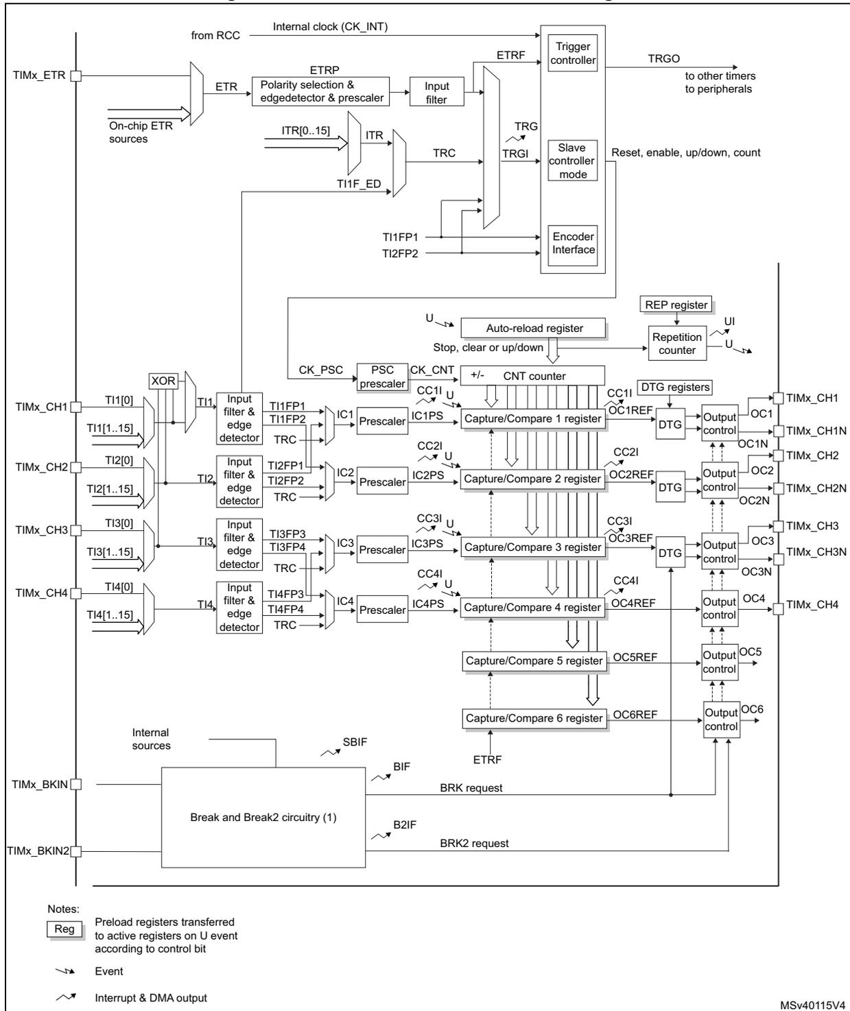
The diagram illustrates the internal architecture of an advanced-control timer (TIM1/TIM8). At the top, the internal clock (CK_INT) from the RCC is fed into the Trigger controller, Slave controller mode, and Encoder Interface. The ETR input is processed through a polarity selection and edgedetector & prescaler, then an input filter, resulting in ETRF. On-chip ETR sources are also fed into this path. The ITR[0..15] and TI1F_ED inputs are combined into TRC, which is then processed by the Trigger controller to produce TRGO to other timers. The TI1FP1 and TI2FP2 inputs are fed into the Encoder Interface. The Slave controller mode receives TRG and TRGI signals and provides Reset, enable, up/down, and count signals to the CNT counter. The CNT counter is a +/- counter that receives CK_PSC from a PSC prescaler and CC1I from the Capture/Compare 1 register. The Auto-reload register (ARR) and REP register are used to configure the counter. The ARR is loaded from the U event and provides the reload value for the counter. The REP register is used for repetition counting. The Capture/Compare 1 register (CCR1) is loaded from the IC1 prescaler, which receives TI1FP1 and TI1FP2 inputs. The CCR1 register provides CC1I to the counter and OC1REF to the output control. The Capture/Compare 2 register (CCR2) is loaded from the IC2 prescaler, which receives TI2FP1 and TI2FP2 inputs. The CCR2 register provides CC2I to the counter and OC2REF to the output control. The Capture/Compare 3 register (CCR3) is loaded from the IC3 prescaler, which receives TI3FP3 and TI3FP4 inputs. The CCR3 register provides CC3I to the counter and OC3REF to the output control. The Capture/Compare 4 register (CCR4) is loaded from the IC4 prescaler, which receives TI4FP3 and TI4FP4 inputs. The CCR4 register provides CC4I to the counter and OC4REF to the output control. The Capture/Compare 5 register (CCR5) and Capture/Compare 6 register (CCR6) are loaded from the U event and provide OC5REF and OC6REF to the output control. The output controls (OC1, OC1N, OC2, OC2N, OC3, OC3N, OC4, OC5, OC6) generate the timer output signals (TIMx_CH1, TIMx_CH1N, TIMx_CH2, TIMx_CH2N, TIMx_CH3, TIMx_CH3N, TIMx_CH4). The Break and Break2 circuitry (1) receives TIMx_BKIN and TIMx_BKIN2 inputs and generates BRK and BRK2 requests. The circuitry also provides SBIF, BIF, and B2IF signals. The diagram includes a legend for symbols: a box with 'Reg' indicates preload registers transferred to active registers on U event; a wavy arrow indicates an event; a jagged arrow indicates an interrupt & DMA output.
1. See Figure 387: Break and Break2 circuitry overview for details
38.3 TIM1/TIM8 functional description
38.3.1 Time-base unit
The main block of the programmable advanced-control timer is a 16-bit counter with its related auto-reload register. The counter can count up, down or both up and down. The counter clock can be divided by a prescaler.
The counter, the auto-reload register and the prescaler register can be written or read by software. This is true even when the counter is running.
The time-base unit includes:
- • Counter register (TIMx_CNT)
- • Prescaler register (TIMx_PSC)
- • Auto-reload register (TIMx_ARR)
- • Repetition counter register (TIMx_RCR)
The auto-reload register is preloaded. Writing to or reading from the auto-reload register accesses the preload register. The content of the preload register are transferred into the shadow register permanently or at each update event (UEV), depending on the auto-reload preload enable bit (ARPE) in TIMx_CR1 register. The update event is sent when the counter reaches the overflow (or underflow when downcounting) and if the UDIS bit equals 0 in the TIMx_CR1 register. It can also be generated by software. The generation of the update event is described in detailed for each configuration.
The counter is clocked by the prescaler output CK_CNT, which is enabled only when the counter enable bit (CEN) in TIMx_CR1 register is set (refer also to the slave mode controller description to get more details on counter enabling).
Note that the counter starts counting 1 clock cycle after setting the CEN bit in the TIMx_CR1 register.
Prescaler description
The prescaler can divide the counter clock frequency by any factor between 1 and 65536. It is based on a 16-bit counter controlled through a 16-bit register (in the TIMx_PSC register). It can be changed on the fly as this control register is buffered. The new prescaler ratio is taken into account at the next update event.
Figure 345 and Figure 346 give some examples of the counter behavior when the prescaler ratio is changed on the fly:
Figure 345. Counter timing diagram with prescaler division change from 1 to 2
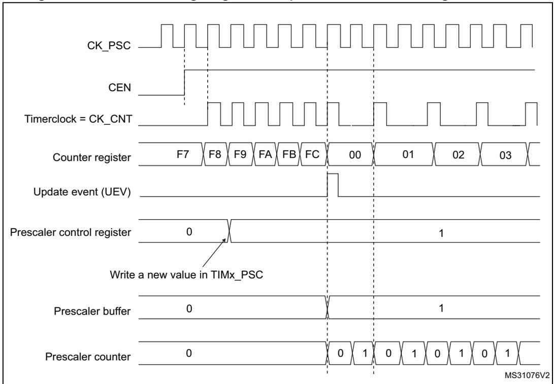
This timing diagram illustrates the operation of a timer counter when the prescaler division is changed from 1 to 2. The diagram includes the following signals and registers over time:
- CK_PSC : Prescaler clock signal, shown as a continuous square wave.
- CEN : Counter Enable signal, which goes high to start the counter.
- Timerclock = CK_CNT : The clock signal for the counter, derived from CK_PSC. Its frequency changes when the prescaler division changes.
- Counter register : Shows the counter values. It counts from F7 to FC, then rolls over to 00. After the prescaler change, it counts 00, 01, 02, 03.
- Update event (UEV) : A pulse generated when the counter rolls over from FC to 00.
- Prescaler control register : Initially set to 0 (division 1). A write operation "Write a new value in TIMx_PSC" changes this value to 1 (division 2) after the first update event.
- Prescaler buffer : Latches the new prescaler value (1) from the control register.
- Prescaler counter : Counts from 0 to 1 (division 1). After the prescaler change, it counts 0, 1, 0, 1, 0, 1, 0, 1 (division 2).
Vertical dashed lines indicate key timing points: the start of counting, the first update event, the write to the prescaler control register, and the subsequent update event where the new prescaler value takes effect. The diagram is labeled MS31076V2.
Figure 346. Counter timing diagram with prescaler division change from 1 to 4
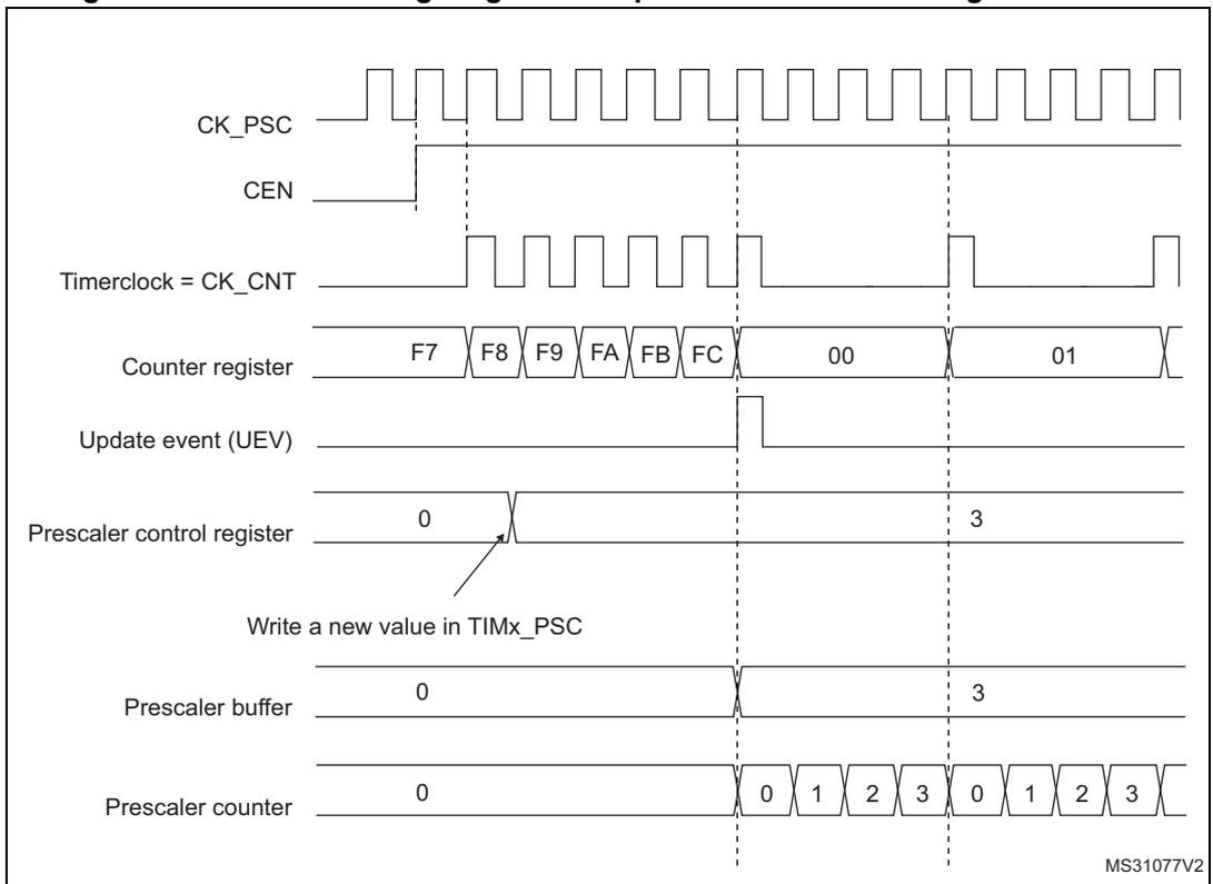
This timing diagram illustrates the operation of a timer counter when the prescaler division is changed from 1 to 4. The signals and registers are similar to Figure 345, but with a different prescaler change:
- CK_PSC , CEN , Timerclock = CK_CNT , Counter register , and Update event (UEV) follow the same sequence as in Figure 345.
- Prescaler control register : Initially set to 0 (division 1). A write operation "Write a new value in TIMx_PSC" changes this value to 3 (division 4) after the first update event.
- Prescaler buffer : Latches the new prescaler value (3) from the control register.
- Prescaler counter : Counts from 0 to 3 (division 1). After the prescaler change, it counts 0, 1, 2, 3, 0, 1, 2, 3 (division 4).
Vertical dashed lines indicate key timing points: the start of counting, the first update event, the write to the prescaler control register, and the subsequent update event where the new prescaler value takes effect. The diagram is labeled MS31077V2.
38.3.2 Counter modes
Upcounting mode
In upcounting mode, the counter counts from 0 to the auto-reload value (content of the TIMx_ARR register), then restarts from 0 and generates a counter overflow event.
If the repetition counter is used, the update event (UEV) is generated after upcounting is repeated for the number of times programmed in the repetition counter register (TIMx_RCR) + 1. Else the update event is generated at each counter overflow.
Setting the UG bit in the TIMx_EGR register (by software or by using the slave mode controller) also generates an update event.
The UEV event can be disabled by software by setting the UDIS bit in the TIMx_CR1 register. This is to avoid updating the shadow registers while writing new values in the preload registers. Then no update event occurs until the UDIS bit has been written to 0. However, the counter restarts from 0, as well as the counter of the prescaler (but the prescale rate does not change). In addition, if the URS bit (update request selection) in TIMx_CR1 register is set, setting the UG bit generates an update event UEV but without setting the UIF flag (thus no interrupt or DMA request is sent). This is to avoid generating both update and capture interrupts when clearing the counter on the capture event.
When an update event occurs, all the registers are updated and the update flag (UIF bit in TIMx_SR register) is set (depending on the URS bit):
- • The repetition counter is reloaded with the content of TIMx_RCR register,
- • The auto-reload shadow register is updated with the preload value (TIMx_ARR),
- • The buffer of the prescaler is reloaded with the preload value (content of the TIMx_PSC register).
The following figures show some examples of the counter behavior for different clock frequencies when TIMx_ARR=0x36.
Figure 347. Counter timing diagram, internal clock divided by 1
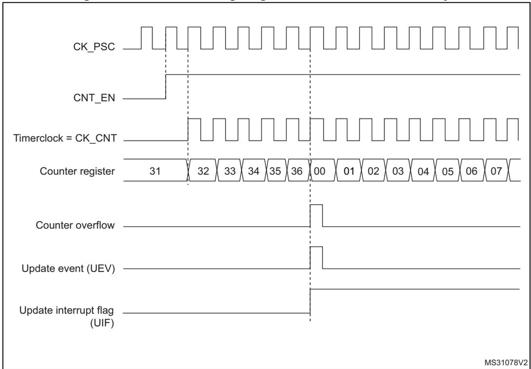
This timing diagram illustrates the operation of a timer with the internal clock divided by 1. The signals shown are:
- CK_PSC : Prescaler clock signal, shown as a square wave.
- CNT_EN : Counter enable signal, which goes high to start counting.
- Timerclock = CK_CNT : The clock signal for the counter, which is the output of the prescaler.
- Counter register : Shows the sequence of values: 31, 32, 33, 34, 35, 36, 00, 01, 02, 03, 04, 05, 06, 07. The values 31 through 36 are in italics, indicating they are part of a previous cycle.
- Counter overflow : A pulse that occurs when the counter reaches its maximum value (36) and rolls over to 00.
- Update event (UEV) : A pulse that occurs at the same time as the counter overflow.
- Update interrupt flag (UIF) : A signal that goes high when an update event occurs.
Vertical dashed lines indicate the timing relationships between the clock edges and the counter value changes. The diagram is labeled MS31078V2 in the bottom right corner.
Figure 348. Counter timing diagram, internal clock divided by 2
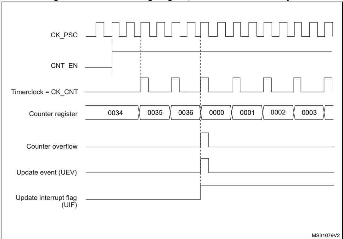
This timing diagram illustrates the operation of a timer with the internal clock divided by 2. The signals shown are:
- CK_PSC : Prescaler clock signal, shown as a square wave.
- CNT_EN : Counter enable signal, which goes high to start counting.
- Timerclock = CK_CNT : The clock signal for the counter, which is half the frequency of the prescaler clock.
- Counter register : Shows the sequence of values: 0034, 0035, 0036, 0000, 0001, 0002, 0003. The values 0034 through 0036 are in italics, indicating they are part of a previous cycle.
- Counter overflow : A pulse that occurs when the counter reaches its maximum value (0036) and rolls over to 0000.
- Update event (UEV) : A pulse that occurs at the same time as the counter overflow.
- Update interrupt flag (UIF) : A signal that goes high when an update event occurs.
Vertical dashed lines indicate the timing relationships between the clock edges and the counter value changes. The diagram is labeled MS31079V2 in the bottom right corner.
Figure 349. Counter timing diagram, internal clock divided by 4
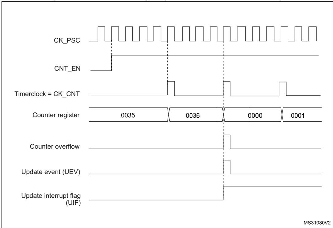
This timing diagram illustrates the counter's operation when the internal clock is divided by 4. The top signal, CK_PSC, is a periodic square wave. Below it, CNT_EN is shown as a high-level signal. The Timerclock (CK_CNT) is a square wave with a frequency one-fourth that of CK_PSC. The Counter register is shown with four values: 0035, 0036, 0000, and 0001. The Counter overflow signal goes high when the counter reaches 0000. The Update event (UEV) also goes high at this point. Finally, the Update interrupt flag (UIF) is set high following the update event. The diagram is labeled MS31080V2 in the bottom right corner.
Figure 350. Counter timing diagram, internal clock divided by N
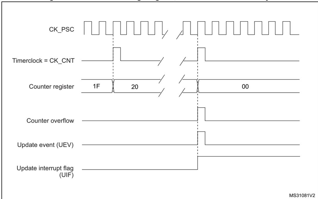
This timing diagram shows the counter's operation with an internal clock divided by an arbitrary value N. The CK_PSC signal is a square wave. The Timerclock (CK_CNT) is a square wave with a frequency divided by N from the CK_PSC frequency. The Counter register displays values 1F, 20, and 00. The Counter overflow signal pulses high when the counter reaches 00. The Update event (UEV) also pulses high at this transition. The Update interrupt flag (UIF) is then set high. The diagram is labeled MS31081V2 in the bottom right corner.
Figure 351. Counter timing diagram, update event when ARPE=0 (TIMx_ARR not preloaded)
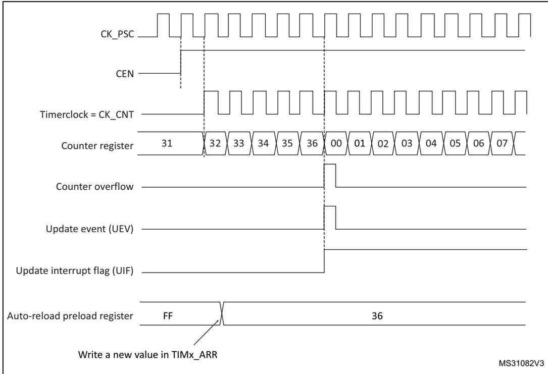
This timing diagram illustrates the operation of an advanced-control timer when ARPE=0. The signals shown are:
- CK_PSC : A periodic clock signal.
- CEN : Counter Enable signal, shown as a high-level signal.
- Timerclock = CK_CNT : The counter clock signal, which is active when CEN is high.
- Counter register : Shows the counter values. It starts at 31, increments through 32, 33, 34, 35, 36, then overflows to 00, 01, 02, 03, 04, 05, 06, 07.
- Counter overflow : A pulse that goes high when the counter reaches 36 and returns low when it reaches 00.
- Update event (UEV) : A pulse that goes high at the overflow point (36 to 00) and returns low.
- Update interrupt flag (UIF) : A signal that goes high at the update event and remains high until cleared.
- Auto-reload preload register : Shows the register value. It is initially FF. An arrow labeled "Write a new value in TIMx_ARR" points to a change in the register to the value 36. This value is loaded into the counter at the next update event.
MS31082V3
Figure 352. Counter timing diagram, update event when ARPE=1 (TIMx_ARR preloaded)
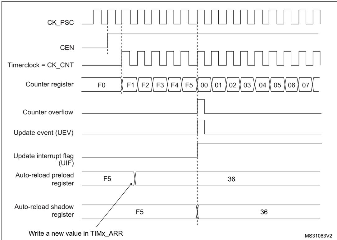
This timing diagram illustrates the operation of an advanced-control timer when ARPE=1. The signals shown are:
- CK_PSC : A periodic clock signal.
- CEN : Counter Enable signal, shown as a high-level signal.
- Timerclock = CK_CNT : The counter clock signal, which is active when CEN is high.
- Counter register : Shows the counter values. It starts at F0, increments through F1, F2, F3, F4, F5, then overflows to 00, 01, 02, 03, 04, 05, 06, 07.
- Counter overflow : A pulse that goes high when the counter reaches F5 and returns low when it reaches 00.
- Update event (UEV) : A pulse that goes high at the overflow point (F5 to 00) and returns low.
- Update interrupt flag (UIF) : A signal that goes high at the update event and remains high until cleared.
- Auto-reload preload register : Shows the register value. It is initially F5. An arrow labeled "Write a new value in TIMx_ARR" points to a change in the register to the value 36. This value is loaded into the register.
- Auto-reload shadow register : Shows the register value. It is initially F5. At the update event (when the counter goes from F5 to 00), the value 36 is loaded into this shadow register.
MS31083V2
Downcounting mode
In downcounting mode, the counter counts from the auto-reload value (content of the TIMx_ARR register) down to 0, then restarts from the auto-reload value and generates a counter underflow event.
If the repetition counter is used, the update event (UEV) is generated after downcounting is repeated for the number of times programmed in the repetition counter register (TIMx_RCR) + 1. Else the update event is generated at each counter underflow.
Setting the UG bit in the TIMx_EGR register (by software or by using the slave mode controller) also generates an update event.
The UEV update event can be disabled by software by setting the UDIS bit in TIMx_CR1 register. This is to avoid updating the shadow registers while writing new values in the preload registers. Then no update event occurs until UDIS bit has been written to 0. However, the counter restarts from the current auto-reload value, whereas the counter of the prescaler restarts from 0 (but the prescale rate doesn't change).
In addition, if the URS bit (update request selection) in TIMx_CR1 register is set, setting the UG bit generates an update event UEV but without setting the UIF flag (thus no interrupt or DMA request is sent). This is to avoid generating both update and capture interrupts when clearing the counter on the capture event.
When an update event occurs, all the registers are updated and the update flag (UIF bit in TIMx_SR register) is set (depending on the URS bit):
- • The repetition counter is reloaded with the content of TIMx_RCR register.
- • The buffer of the prescaler is reloaded with the preload value (content of the TIMx_PSC register).
- • The auto-reload active register is updated with the preload value (content of the TIMx_ARR register). Note that the auto-reload is updated before the counter is reloaded, so that the next period is the expected one.
The following figures show some examples of the counter behavior for different clock frequencies when TIMx_ARR=0x36.
Figure 353. Counter timing diagram, internal clock divided by 1
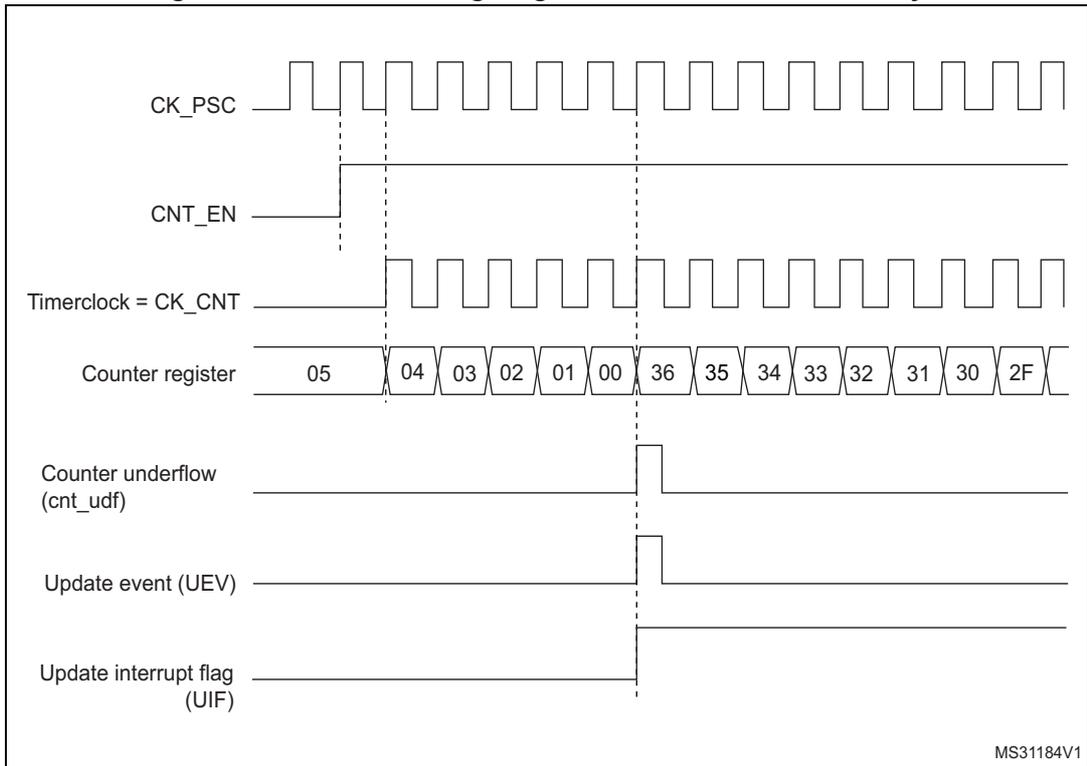
This timing diagram illustrates the operation of an advanced-control timer with the internal clock divided by 1. The diagram shows the following signals and their relationship over time:
- CK_PSC : Prescaler clock signal, shown as a square wave.
- CNT_EN : Counter enable signal, which is a high-level signal that enables the counter.
- Timerclock = CK_CNT : The clock signal for the counter, which is the output of the prescaler.
- Counter register : A sequence of values: 05, 04, 03, 02, 01, 00, 36, 35, 34, 33, 32, 31, 30, 2F. The counter counts down from 05 to 00, then underflows to 36 and continues counting down.
- Counter underflow (cnt_udf) : A signal that goes high when the counter register reaches 00 and then returns low.
- Update event (UEV) : A signal that goes high when the counter underflows (at the transition from 00 to 36).
- Update interrupt flag (UIF) : A signal that goes high when the update event (UEV) occurs and remains high until it is manually cleared.
Vertical dashed lines indicate the timing relationships between the signals. The first dashed line is at the rising edge of CK_PSC when CNT_EN goes high. The second dashed line is at the falling edge of CK_CNT when the counter register reaches 00. The third dashed line is at the rising edge of CK_CNT when the counter register reaches 36.
MS31184V1
Figure 354. Counter timing diagram, internal clock divided by 2
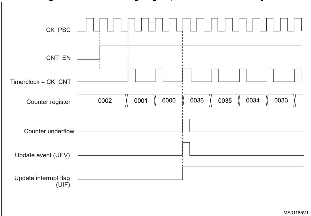
This timing diagram illustrates the operation of an advanced-control timer with the internal clock divided by 2. The diagram shows the following signals and their relationship over time:
- CK_PSC : Prescaler clock signal, shown as a square wave.
- CNT_EN : Counter enable signal, which is a high-level signal that enables the counter.
- Timerclock = CK_CNT : The clock signal for the counter, which is the output of the prescaler. Its frequency is half that of CK_PSC.
- Counter register : A sequence of values: 0002, 0001, 0000, 0036, 0035, 0034, 0033. The counter counts down from 0002 to 0000, then underflows to 0036 and continues counting down.
- Counter underflow : A signal that goes high when the counter register reaches 0000 and then returns low.
- Update event (UEV) : A signal that goes high when the counter underflows (at the transition from 0000 to 0036).
- Update interrupt flag (UIF) : A signal that goes high when the update event (UEV) occurs and remains high until it is manually cleared.
Vertical dashed lines indicate the timing relationships between the signals. The first dashed line is at the rising edge of CK_PSC when CNT_EN goes high. The second dashed line is at the falling edge of CK_CNT when the counter register reaches 0000. The third dashed line is at the rising edge of CK_CNT when the counter register reaches 0036.
MS31185V1
Figure 355. Counter timing diagram, internal clock divided by 4
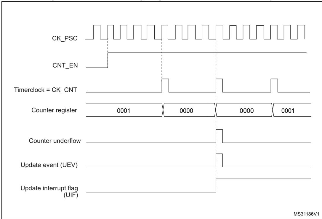
Timing diagram for internal clock divided by 4. The diagram shows the relationship between the prescaler clock (CK_PSC), counter enable (CNT_EN), timer clock (CK_CNT), counter register values, counter underflow, update event (UEV), and update interrupt flag (UIF). The counter register values are 0001, 0000, 0000, 0001. The counter underflow and UEV occur when the counter register is 0000. The UIF is set when the counter register is 0000. MS31186V1
Figure 356. Counter timing diagram, internal clock divided by N
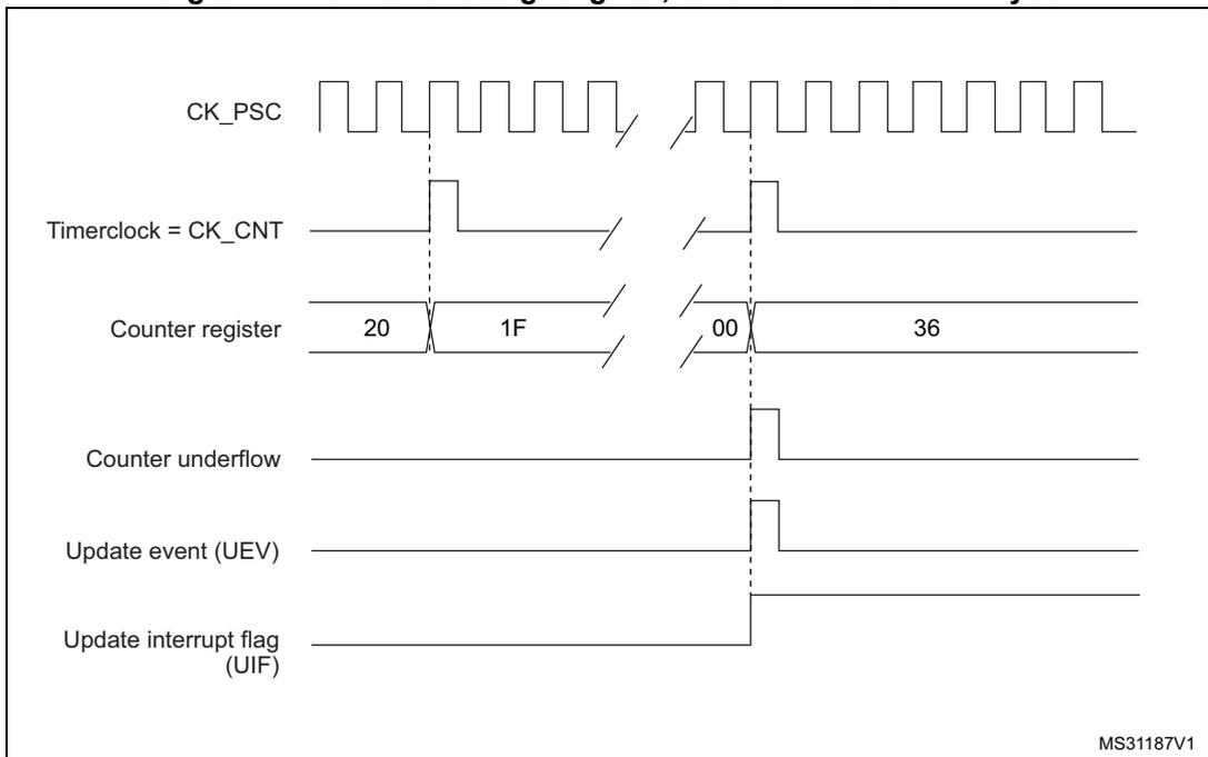
Timing diagram for internal clock divided by N. The diagram shows the relationship between the prescaler clock (CK_PSC), timer clock (CK_CNT), counter register values, counter underflow, update event (UEV), and update interrupt flag (UIF). The counter register values are 20, 1F, 00, 36. The counter underflow and UEV occur when the counter register is 00. The UIF is set when the counter register is 00. MS31187V1
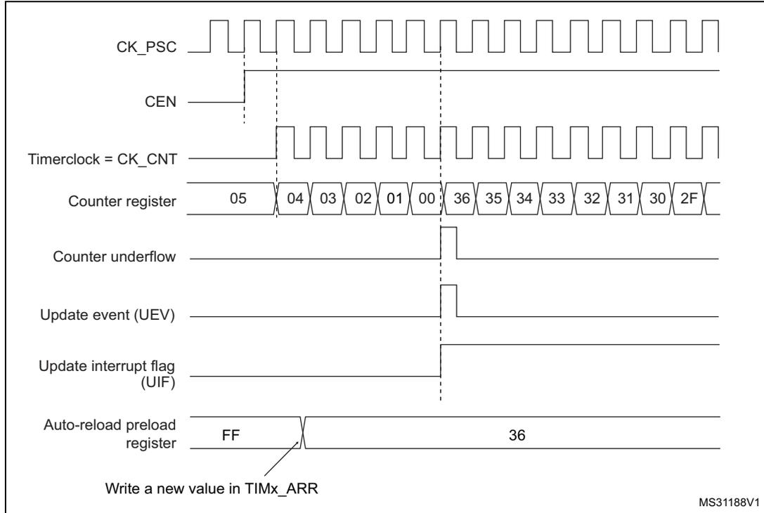
The timing diagram illustrates the operation of an advanced-control timer. The top signal, CK_PSC, is a periodic clock. Below it, CEN (Counter Enable) is shown as a high-level signal. The Timerclock = CK_CNT is derived from CK_PSC. The Counter register shows a sequence of values: 05, 04, 03, 02, 01, 00, 36, 35, 34, 33, 32, 31, 30, 2F. The Counter underflow signal goes high when the counter reaches 00. The Update event (UEV) and Update interrupt flag (UIF) are also shown going high at the 00 count. The Auto-reload preload register is shown with values FF and 36, with a note indicating that a new value can be written in TIMx_ARR.
Center-aligned mode (up/down counting)
In center-aligned mode, the counter counts from 0 to the auto-reload value (content of the TIMx_ARR register) – 1, generates a counter overflow event, then counts from the auto-reload value down to 1 and generates a counter underflow event. Then it restarts counting from 0.
Center-aligned mode is active when the CMS bits in TIMx_CR1 register are not equal to '00'. The Output compare interrupt flag of channels configured in output is set when: the counter counts down (Center aligned mode 1, CMS = "01"), the counter counts up (Center aligned mode 2, CMS = "10") the counter counts up and down (Center aligned mode 3, CMS = "11").
In this mode, the DIR direction bit in the TIMx_CR1 register cannot be written. It is updated by hardware and gives the current direction of the counter.
The update event can be generated at each counter overflow and at each counter underflow or by setting the UG bit in the TIMx_EGR register (by software or by using the slave mode controller) also generates an update event. In this case, the counter restarts counting from 0, as well as the counter of the prescaler.
The UEV update event can be disabled by software by setting the UDIS bit in the TIMx_CR1 register. This is to avoid updating the shadow registers while writing new values in the preload registers. Then no update event occurs until UDIS bit has been written to 0. However, the counter continues counting up and down, based on the current auto-reload value.
In addition, if the URS bit (update request selection) in TIMx_CR1 register is set, setting the UG bit generates an UEV update event but without setting the UIF flag (thus no interrupt or
DMA request is sent). This is to avoid generating both update and capture interrupts when clearing the counter on the capture event.
When an update event occurs, all the registers are updated and the update flag (UIF bit in TIMx_SR register) is set (depending on the URS bit):
- • The repetition counter is reloaded with the content of TIMx_RCR register
- • The buffer of the prescaler is reloaded with the preload value (content of the TIMx_PSC register)
- • The auto-reload active register is updated with the preload value (content of the TIMx_ARR register). Note that if the update source is a counter overflow, the auto-reload is updated before the counter is reloaded, so that the next period is the expected one (the counter is loaded with the new value).
The following figures show some examples of the counter behavior for different clock frequencies.
Figure 358. Counter timing diagram, internal clock divided by 1, TIMx_ARR = 0x6
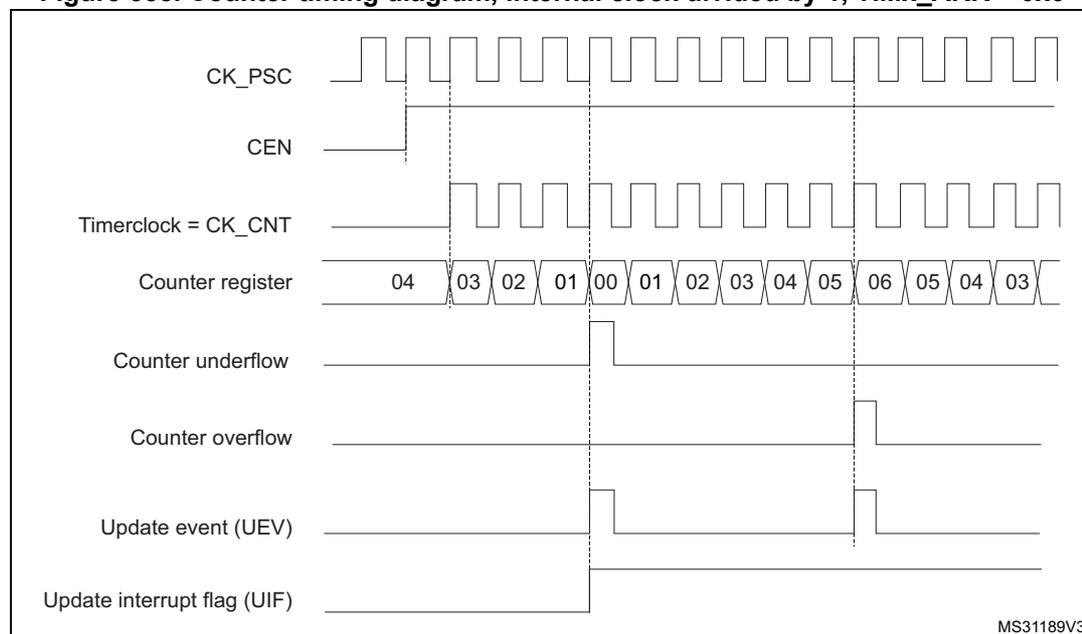
The timing diagram illustrates the operation of a timer in center-aligned mode 1. The signals shown are:
- CK_PSC : Prescaler clock signal, a periodic square wave.
- CEN : Counter enable signal, which goes high to start counting.
- Timerclock = CK_CNT : Counter clock signal, derived from CK_PSC.
- Counter register : Shows the counter values over time: 04, 03, 02, 01, 00, 01, 02, 03, 04, 05, 06, 05, 04, 03. The counter counts up to 0x6 (06) and then back down to 0x0 (00).
- Counter underflow : A pulse that goes high when the counter reaches 0x00.
- Counter overflow : A pulse that goes high when the counter reaches 0x06.
- Update event (UEV) : A pulse that goes high when either the underflow or overflow occurs.
- Update interrupt flag (UIF) : A signal that goes high in response to the UEV pulse.
The diagram shows two full cycles of counting. Vertical dashed lines indicate the rising edges of the timer clock (CK_CNT). The counter values are shown in a sequence of trapezoidal shapes, indicating the count at each clock edge. The first cycle shows the counter counting up from 0x00 to 0x06 and then back down to 0x00. The second cycle shows the counter counting up from 0x00 to 0x06 and then back down to 0x03. The underflow and overflow signals are shown as pulses that go high at the respective count values (0x00 and 0x06). The update event (UEV) is shown as a pulse that goes high when either the underflow or overflow occurs. The update interrupt flag (UIF) is shown as a signal that goes high in response to the UEV pulse.
MS31189V3
- 1. Here, center-aligned mode 1 is used (for more details refer to Section 38.4: TIM1/TIM8 registers ).
Figure 359. Counter timing diagram, internal clock divided by 2
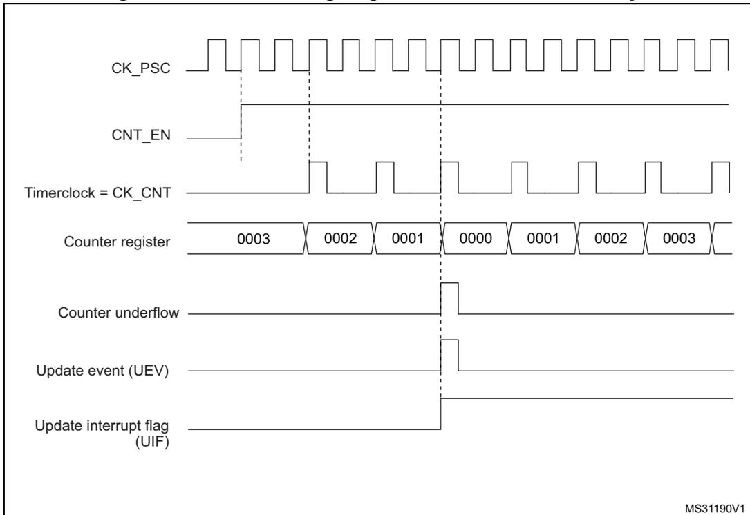
This timing diagram illustrates the operation of a timer counter. The top signal, CK_PSC, is a periodic square wave. Below it, CNT_EN is a signal that goes high to enable the counter. The Timerclock = CK_CNT signal is derived from CK_PSC and has a frequency half that of CK_PSC. The Counter register shows a sequence of values: 0003, 0002, 0001, 0000, 0001, 0002, 0003. Vertical dashed lines indicate the rising edges of the Timerclock. At the transition from 0000 to 0001, the Counter underflow signal pulses high. Simultaneously, the Update event (UEV) and the Update interrupt flag (UIF) also pulse high. The diagram is labeled MS31190V1 in the bottom right corner.
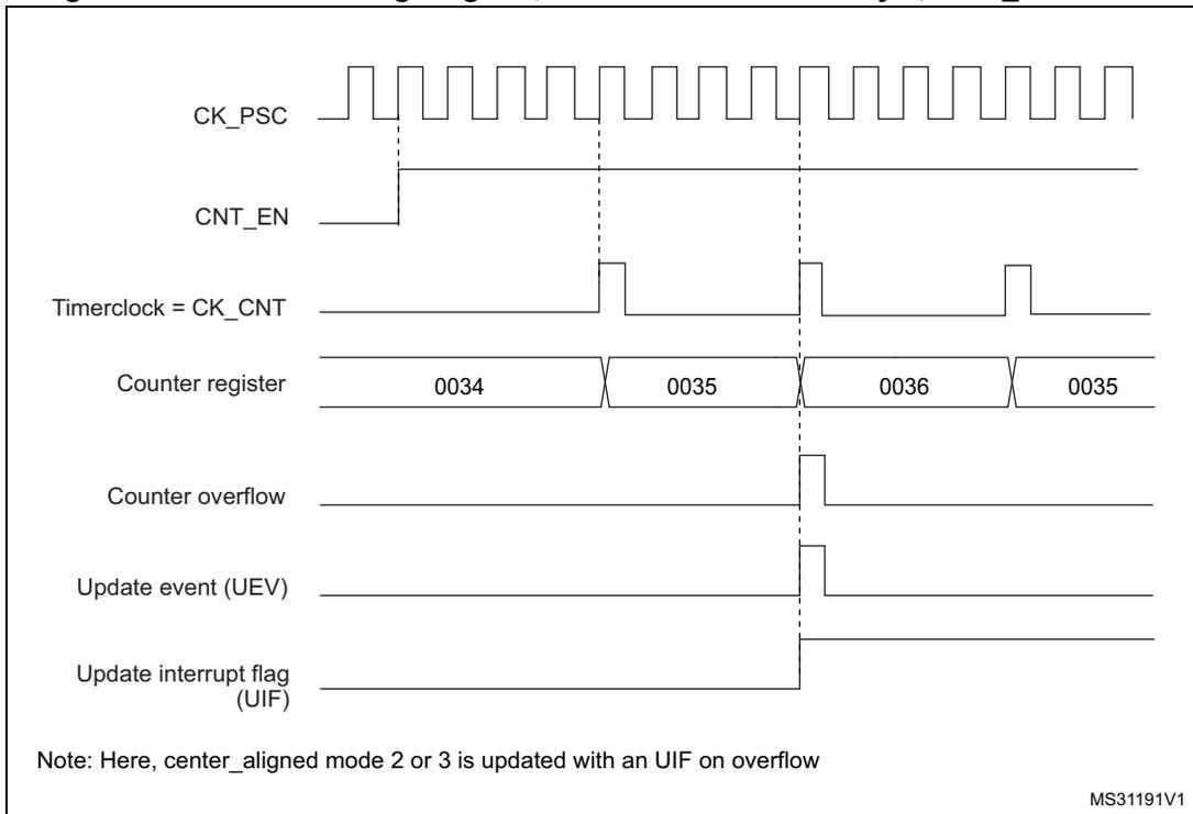
Figure 360. Counter timing diagram, internal clock divided by 4, TIMx_ARR=0x36
This timing diagram shows the counter operation with an internal clock divided by 4 and an auto-reload register value of 0x36. The signals CK_PSC, CNT_EN, and Timerclock = CK_CNT are shown. The Counter register values are 0034, 0035, 0036, and then back to 0035. Vertical dashed lines mark the rising edges of the Timerclock. At the transition from 0036 to 0035, the Counter overflow signal pulses high. This is followed by a pulse on the Update event (UEV) and the Update interrupt flag (UIF). A note at the bottom states: "Note: Here, center_aligned mode 2 or 3 is updated with an UIF on overflow". The diagram is labeled MS31191V1 in the bottom right corner.
Figure 361. Counter timing diagram, internal clock divided by N
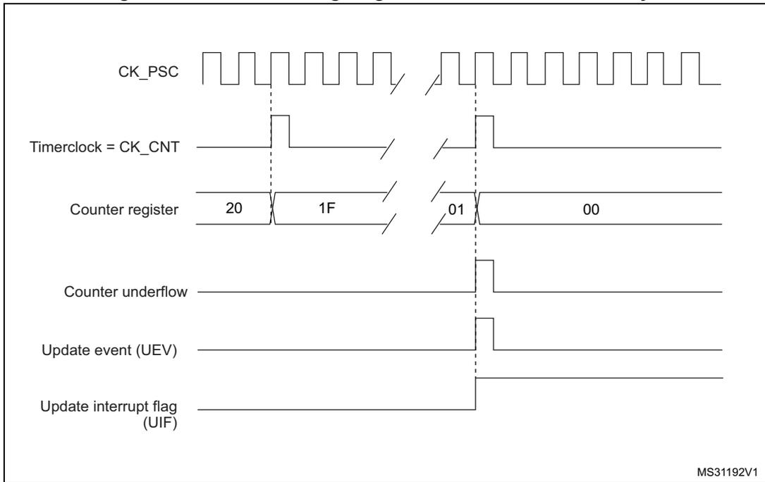
This timing diagram illustrates the operation of a counter with an internal clock divided by N. The top signal, CK_PSC, is a periodic square wave. Below it, the Timerclock = CK_CNT is shown as a series of pulses, with one pulse corresponding to each falling edge of CK_PSC. The Counter register is shown with values 20, 1F, 01, and 00. The counter decrements from 20 to 1F, then from 01 to 00. A Counter underflow event occurs when the counter reaches 00. The Update event (UEV) and Update interrupt flag (UIF) are shown as pulses that occur at the time of the counter underflow. The diagram is labeled MS31192V1 in the bottom right corner.
Figure 362. Counter timing diagram, update event with ARPE=1 (counter underflow)
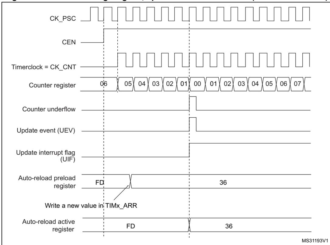
This timing diagram shows the counter operation with ARPE=1. The signals CK_PSC, Timerclock = CK_CNT, Counter underflow, Update event (UEV), and Update interrupt flag (UIF) are similar to Figure 361. The Counter register counts down from 06 to 00 and then up from 01 to 07. The Auto-reload preload register contains the value FD initially, which is then updated to 36. The Write a new value in TIMx_ARR signal is shown as a pulse that occurs when the new value 36 is written. The Auto-reload active register contains the value FD initially, which is then updated to 36. The diagram is labeled MS31193V1 in the bottom right corner.
Figure 363. Counter timing diagram, Update event with ARPE=1 (counter overflow)
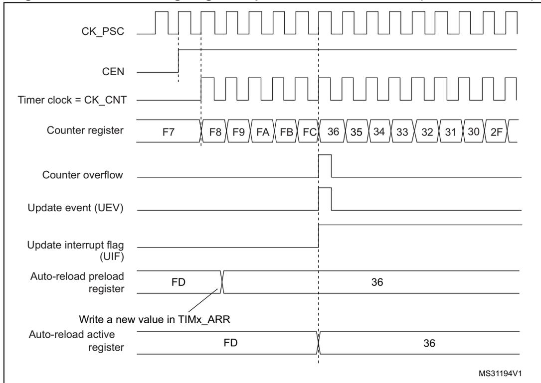
The timing diagram illustrates the operation of an advanced-control timer (TIM1/TIM8) in counter overflow mode with ARPE=1. The signals shown are:
- CK_PSC : Prescaler clock signal, shown as a square wave.
- CEN : Counter enable signal, shown as a high-level signal.
- Timer clock = CK_CNT : Counter clock signal, derived from CK_PSC, shown as a square wave.
- Counter register : Shows the sequence of counter values: F7, F8, F9, FA, FB, FC, 36, 35, 34, 33, 32, 31, 30, 2F. The values F7 through FC are hexadecimal, and 36 through 2F are decimal.
- Counter overflow : A signal that goes high when the counter reaches its maximum value (FC) and then rolls over to 36.
- Update event (UEV) : A signal that goes high when the counter overflows.
- Update interrupt flag (UIF) : A signal that goes high when the counter overflows.
- Auto-reload preload register : Shows the value FD (hexadecimal) being written to the register, and then the value 36 (decimal) being loaded into the active register.
- Write a new value in TIMx_ARR : A signal indicating the write operation to the preload register.
- Auto-reload active register : Shows the value FD (hexadecimal) being written to the register, and then the value 36 (decimal) being loaded into the active register.
MS31194V1
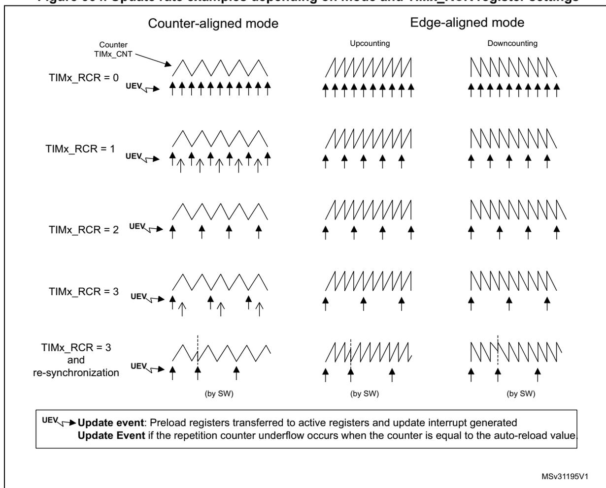
38.3.3 Repetition counter
Section 38.3.1: Time-base unit describes how the update event (UEV) is generated with respect to the counter overflows/underflows. It is actually generated only when the repetition counter has reached zero. This can be useful when generating PWM signals.
This means that data are transferred from the preload registers to the shadow registers (TIMx_ARR auto-reload register, TIMx_PSC prescaler register, but also TIMx_CCRx capture/compare registers in compare mode) every N+1 counter overflows or underflows, where N is the value in the TIMx_RCR repetition counter register.
The repetition counter is decremented:
- • At each counter overflow in upcounting mode,
- • At each counter underflow in downcounting mode,
- • At each counter overflow and at each counter underflow in center-aligned mode.
- Although this limits the maximum number of repetition to 32768 PWM cycles, it makes it possible to update the duty cycle twice per PWM period. When refreshing compare registers only once per PWM period in center-aligned mode, maximum resolution is \( 2 \times T_{ck} \) , due to the symmetry of the pattern.
The repetition counter is an auto-reload type; the repetition rate is maintained as defined by the TIMx_RCR register value (refer to Figure 364 ). When the update event is generated by software (by setting the UG bit in TIMx_EGR register) or by hardware through the slave mode controller, it occurs immediately whatever the value of the repetition counter is and the repetition counter is reloaded with the content of the TIMx_RCR register.
In Center aligned mode, for odd values of RCR, the update event occurs either on the overflow or on the underflow depending on when the RCR register was written and when the counter was launched: if the RCR was written before launching the counter, the UEV occurs on the underflow. If the RCR was written after launching the counter, the UEV occurs on the overflow.
For example, for RCR = 3, the UEV is generated each 4th overflow or underflow event depending on when the RCR was written.
Figure 364. Update rate examples depending on mode and TIMx_RCR register settings
| Counter-aligned mode | Edge-aligned mode | ||
|---|---|---|---|
| Upcounting | Downcounting | ||
| TIMx_RCR = 0 | |||
| TIMx_RCR = 1 | |||
| TIMx_RCR = 2 | |||
| TIMx_RCR = 3 | |||
| TIMx_RCR = 3 and re-synchronization | |||
UEV →
Update event:
Preload registers transferred to active registers and update interrupt generated
Update Event
if the repetition counter underflow occurs when the counter is equal to the auto-reload value.
MSv31195V1
38.3.4 External trigger input
The timer features an external trigger input ETR. It can be used as:
- • external clock (external clock mode 2, see Section 38.3.5 )
- • trigger for the slave mode (see Section 38.3.26 )
- • PWM reset input for cycle-by-cycle current regulation (see Section 38.3.7 )
Figure 365 below describes the ETR input conditioning. The input polarity is defined with the ETP bit in TIMxSMCR register. The trigger can be prescaled with the divider programmed by the ETPS[1:0] bitfield and digitally filtered with the ETF[3:0] bitfield.
Figure 365. External trigger input block
![Block diagram of the external trigger input conditioning. The ETR input passes through a polarity selector (controlled by ETP in TIMx_SMCR) and then a divider (controlled by ETPS[1:0] in TIMx_SMCR). The output of the divider (ETRP) is then passed through a filter downcounter (controlled by ETF[3:0] in TIMx_SMCR). The final output is sent to the Output mode controller, the CK_PSC circuitry, and the Slave mode controller. The diagram is labeled MS34403V2.](/RM0433-STM32H742-743-753-750/be6bd7787dd2c8fe40cb8c47e8cec9f3_img.jpg)
The ETR input comes from multiple sources: input pins (default configuration), comparator outputs and analog watchdogs. The selection is done with the ETRSEL[3:0] bitfield.
Figure 366. TIM1/TIM8 ETR input circuitry
![Diagram showing the ETR input circuitry for TIM1 and TIM8. Both timers have an AF controller (TIM1_AF1[17:14] and TIM8_AF1[17:14]) that selects from various internal sources: ETR inputs from AF controller, COMP1 output, COMP2 output, ADC1 AWD1, ADC1 AWD2, ADC1 AWD3, ADC3 AWD1, ADC3 AWD2, and ADC3 AWD3. The selected signal is then routed to the ETR input of the timer. The diagram is labeled MSV40116V2.](/RM0433-STM32H742-743-753-750/8017fd706de0287e15c1203aa65238ae_img.jpg)
38.3.5 Clock selection
The counter clock can be provided by the following clock sources:
- • Internal clock (CK_INT)
- • External clock mode1: external input pin
- • External clock mode2: external trigger input ETR
- • Encoder mode
Internal clock source (CK_INT)
If the slave mode controller is disabled (SMS=000), then the CEN, DIR (in the TIMx_CR1 register) and UG bits (in the TIMx_EGR register) are actual control bits and can be changed only by software (except UG which remains cleared automatically). As soon as the CEN bit is written to 1, the prescaler is clocked by the internal clock CK_INT.
Figure 367 shows the behavior of the control circuit and the upcounter in normal mode, without prescaler.
Figure 367. Control circuit in normal mode, internal clock divided by 1
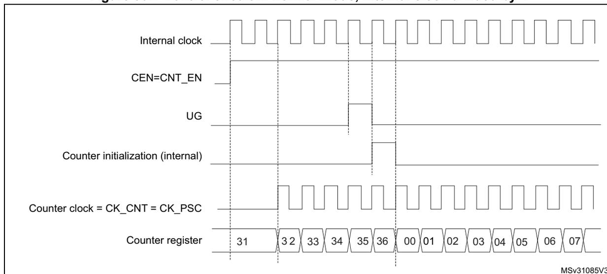
The timing diagram illustrates the relationship between several signals over time. The top signal, 'Internal clock', is a continuous square wave. Below it, 'CEN=CNT_EN' is a signal that goes high at a certain point. The 'UG' signal is initially low and goes high when CEN goes high, then returns to low. The 'Counter initialization (internal)' signal is initially high and goes low when UG goes high. The 'Counter clock = CK_CNT = CK_PSC' signal is initially low and goes high when CEN goes high. The bottom signal, 'Counter register', shows a sequence of values: 31, 32, 33, 34, 35, 36, 00, 01, 02, 03, 04, 05, 06, 07. The counter increments by 1 at each rising edge of the counter clock, starting from 31 and rolling over from 36 to 00. Vertical dashed lines indicate the timing relationships between the signals.
External clock source mode 1
This mode is selected when SMS=111 in the TIMx_SMCR register. The counter can count at each rising or falling edge on a selected input.
Figure 368. TI2 external clock connection example
![Block diagram showing the TI2 external clock connection. It includes TIMx_CH2 input, TI2 signal path with filter (ICF[3:0]), edge detector (TI2F_Rising, TI2F_Falling), and a multiplexer for trigger selection (TIMx_SMCR) leading to CK_PSC output. The multiplexer selects between ITRx, TI1_ED, TI1FP1, TI2FP2, ETRF, and CK_INT (internal clock) based on TS[4:0] bits. CC2P and TIMx_CCER are also shown.](/RM0433-STM32H742-743-753-750/202cc0ce146cd257f1fd876c5af1e882_img.jpg)
The diagram illustrates the internal logic for using the TI2 input as an external clock source. The TI2 signal from TIMx_CH2 passes through a programmable filter (ICF[3:0] in TIMx_CCMR1) and an edge detector. The edge detector outputs TI2F_Rising and TI2F_Falling signals. These are connected to a multiplexer that selects the trigger source for the timer. The multiplexer is controlled by the TIMx_SMCR register, specifically the TS[4:0] bits. The selected trigger source (TRGI) is then used to generate the CK_PSC (capture prescaler clock). Other possible trigger sources include ITRx, TI1_ED, TI1FP1, TI2FP2, ETRF, and the internal clock (CK_INT). The CC2P bit in TIMx_CCER is used to configure the polarity for the rising edge detection.
- 1. Codes ranging from 01000 to 11111 are reserved
For example, to configure the upcounter to count in response to a rising edge on the TI2 input, use the following procedure:
- 1. Select the proper TI2x source (internal or external) with the TI2SEL[3:0] bits in the TIMx_TISEL register.
- 2. Configure channel 2 to detect rising edges on the TI2 input by writing CC2S = '01' in the TIMx_CCMR1 register.
- 3. Configure the input filter duration by writing the IC2F[3:0] bits in the TIMx_CCMR1 register (if no filter is needed, keep IC2F=0000).
- 4. Select rising edge polarity by writing CC2P=0 and CC2NP=0 in the TIMx_CCER register.
- 5. Configure the timer in external clock mode 1 by writing SMS=111 in the TIMx_SMCR register.
- 6. Select TI2 as the trigger input source by writing TS=00110 in the TIMx_SMCR register.
- 7. Enable the counter by writing CEN=1 in the TIMx_CR1 register.
Note: The capture prescaler is not used for triggering, so the user does not need to configure it.
When a rising edge occurs on TI2, the counter counts once and the TIF flag is set.
The delay between the rising edge on TI2 and the actual clock of the counter is due to the resynchronization circuit on TI2 input.
Figure 369. Control circuit in external clock mode 1
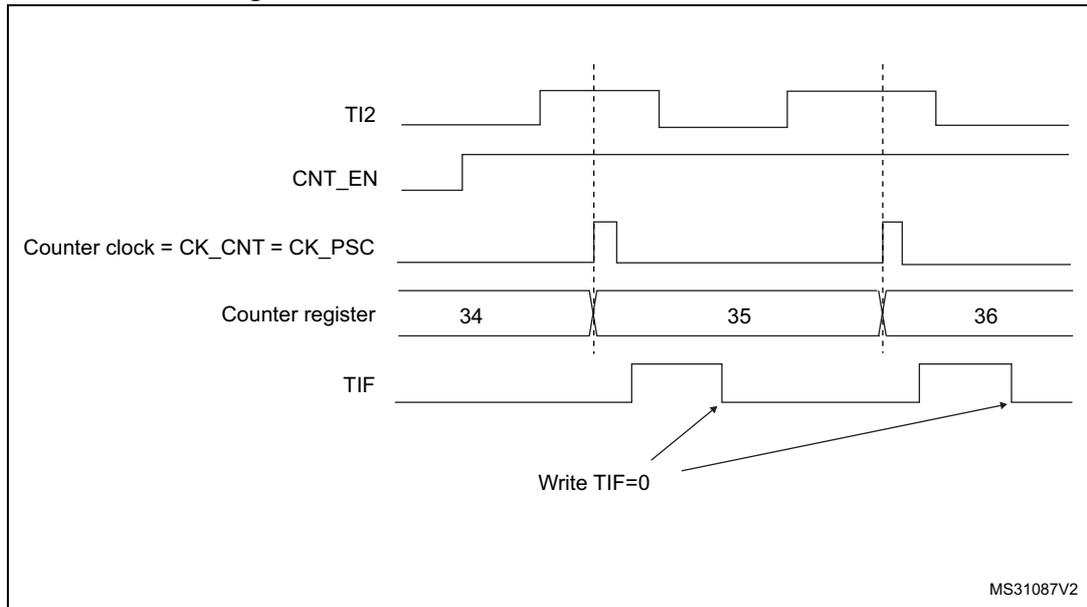
The diagram shows the relationship between several signals over time. The top signal, TI2, is a periodic square wave. Below it, CNT_EN is a signal that goes high and stays high. The third signal, 'Counter clock = CK_CNT = CK_PSC', is a square wave that toggles on the rising edges of TI2. The fourth signal, 'Counter register', shows the count value increasing from 34 to 35 to 36, with each increment occurring at a rising edge of the counter clock. The bottom signal, TIF, is an interrupt flag that goes high at the rising edge of the counter clock following a count overflow (from 36 back to 34) and returns low when 'Write TIF=0' is performed. A label 'MS31087V2' is in the bottom right corner.
External clock source mode 2
This mode is selected by writing ECE=1 in the TIMx_SMCR register.
The counter can count at each rising or falling edge on the external trigger input ETR.
The Figure 370 gives an overview of the external trigger input block.
Figure 370. External trigger input block
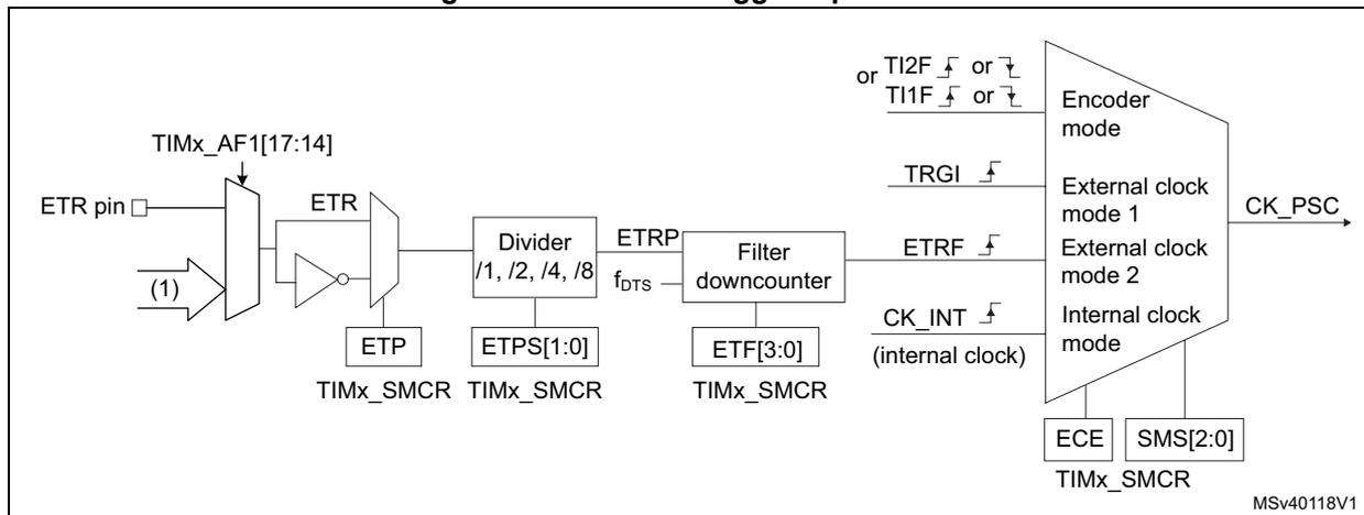
The block diagram illustrates the external trigger input path. It starts with the 'ETR pin' connected to a multiplexer. The multiplexer has several inputs: a direct connection from the pin, an inverted connection, a connection labeled '(1)' (refer to Figure 366), and an output from a filter downcounter. The multiplexer output is labeled 'ETR'. This signal passes through another multiplexer controlled by 'TIMx_AF1[17:14]'. The output of this second multiplexer is 'ETRP', which is also controlled by 'TIMx_SMCR' (specifically the ETP bit). 'ETRP' then enters a 'Divider' block with options '/1, /2, /4, /8', controlled by 'ETPS[1:0]' in 'TIMx_SMCR'. The output of the divider is 'f_DTS', which enters a 'Filter downcounter' block controlled by 'ETF[3:0]' in 'TIMx_SMCR'. The output of the filter is 'ETRF'. Both 'ETRF' and an 'internal clock' ('CK_INT') are inputs to a large multiplexer on the right. This multiplexer is controlled by 'TIMx_SMCR' registers 'ECE' and 'SMS[2:0]'. The selected output is 'CK_PSC'. Other inputs to this multiplexer include 'TI2F' or 'TI1F' signals and 'TRGI'.
1. Refer to Figure 366: TIM1/TIM8 ETR input circuitry.
For example, to configure the upcounter to count each 2 rising edges on ETR, use the following procedure:
- 1. As no filter is needed in this example, write ETF[3:0]=0000 in the TIMx_SMCR register.
- 2. Set the prescaler by writing ETPS[1:0]=01 in the TIMx_SMCR register
- 3. Select rising edge detection on the ETR pin by writing ETP=0 in the TIMx_SMCR register
- 4. Enable external clock mode 2 by writing ECE=1 in the TIMx_SMCR register.
- 5. Enable the counter by writing CEN=1 in the TIMx_CR1 register.
The counter counts once each 2 ETR rising edges.
The delay between the rising edge on ETR and the actual clock of the counter is due to the resynchronization circuit on the ETRP signal. As a consequence, the maximum frequency which can be correctly captured by the counter is at most 1/4 of TIMxCLK frequency. When the ETRP signal is faster, the user should apply a division of the external signal by proper ETPS prescaler setting.
Figure 371. Control circuit in external clock mode 2
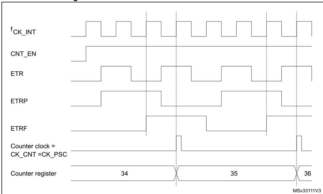
The timing diagram illustrates the control circuit in external clock mode 2. It shows the following signals and their relationship over time:
- f CK_INT : Internal clock signal, shown as a periodic square wave.
- CNT_EN : Counter enable signal, which goes high to enable counting.
- ETR : External trigger signal, shown as a square wave.
- ETRP : Resynchronized external trigger signal, which follows ETR with some delay and jitter.
- ETRF : External trigger filter output, which is a filtered version of ETR.
- Counter clock = CK_CNT = CK_PSC : The clock signal for the counter, which is derived from the internal clock and prescaled.
- Counter register : The register that counts the number of valid clock cycles. It shows values 34, 35, and 36.
The counter increments its value (from 34 to 35, then to 36) on every second rising edge of the ETR signal, synchronized with the counter clock. Vertical dashed lines indicate the timing relationships between the signals.
MSv3311V3
38.3.6 Capture/compare channels
Each Capture/Compare channel is built around a capture/compare register (including a shadow register), an input stage for capture (with digital filter, multiplexing, and prescaler, except for channels 5 and 6) and an output stage (with comparator and output control).
Figure 372 to Figure 375 give an overview of one Capture/Compare channel.
The input stage samples the corresponding TIx input to generate a filtered signal TIxF. Then, an edge detector with polarity selection generates a signal (TIxFPx) which can be used as trigger input by the slave mode controller or as the capture command. It is prescaled before the capture register (ICxPS).
Figure 372. Capture/compare channel (example: channel 1 input stage)
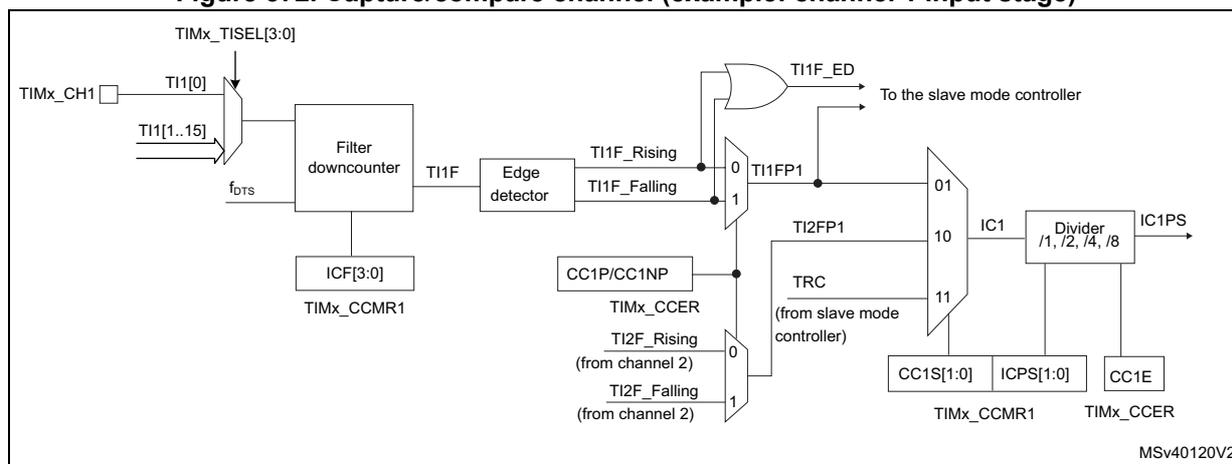
This block diagram illustrates the input stage of a capture/compare channel. The input signal TIMx_CH1 is multiplexed with TI1[1..15] and filtered by a 'Filter downcounter' (controlled by TIMx_TISEL[3:0] and ICF[3:0] from TIMx_CCMR1). The filtered signal TI1F is processed by an 'Edge detector' (controlled by CC1P/CC1NP and TIMx_CCER) to generate TI1F_Rising and TI1F_Falling signals. These are combined with TI2F_Rising and TI2F_Falling signals (from channel 2) via a multiplexer (controlled by TRC from the slave mode controller) to produce TI1FP1. This signal is then processed by a 'Divide by 2' block (controlled by IC1S[1:0] from TIMx_CCMR1) to generate the final output IC1PS. The IC1PS signal is also used as the capture command for the capture/compare register.
The output stage generates an intermediate waveform which is then used for reference: OCxRef (active high). The polarity acts at the end of the chain.
Figure 373. Capture/compare channel 1 main circuit
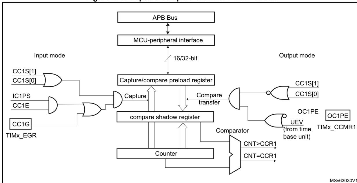
This block diagram shows the main circuit of a capture/compare channel. It is divided into 'Input mode' and 'Output mode'. In 'Input mode', the APB Bus connects to an 'MCU-peripheral interface', which in turn connects to a 'Capture/compare preload register' and a 'compare shadow register'. These registers are connected to a 'Counter' (16/32-bit). The 'Counter' output is compared with the 'compare shadow register' output in a 'Comparator' block, which generates CNT>CCR1 and CNT=CCR1 signals. The 'Capture' signal is generated by a combination of CC1S[1], CC1S[0], IC1PS, CC1E, and CC1G (from TIMx_EGR). In 'Output mode', the 'compare shadow register' output is compared with the 'Counter' output in a 'Comparator' block, which generates OC1PE. The OC1PE signal is combined with UEV (from time base unit) and OC1S[1], CC1S[0] to generate the final output OC1PE. The OC1PE signal is also used as the output control for the output stage.
Figure 374. Output stage of capture/compare channel (channel 1, idem ch. 2 and 3)
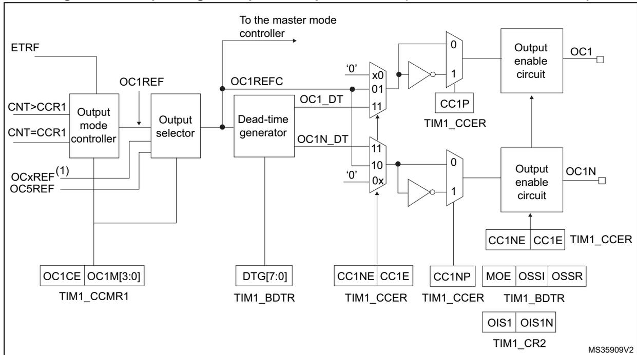
The diagram illustrates the output stage for capture/compare channels 1, 2, and 3. The signal flow starts with ETRF and CNT/CCR1 inputs to an 'Output mode controller'. This controller outputs OC1REF, which is then processed by an 'Output selector'. The 'Output selector' also receives OCxREF (1) (OC5REF) and OC1REFC signals. The 'Output selector' outputs OC1REFC to the master mode controller and OC1_DT and OC1N_DT signals to a 'Dead-time generator'. The 'Dead-time generator' is controlled by DTG[7:0] from TIM1_BDTR. The 'Dead-time generator' outputs OC1_DT and OC1N_DT signals to multiplexers. These multiplexers are controlled by '0', 'x0', '01', and '11' signals from CC1NE, CC1E, and CC1P registers in TIM1_CCER. The multiplexers output signals to 'Output enable circuit' blocks, which produce OC1 and OC1N outputs. The 'Output enable circuit' blocks are also controlled by CC1NE, CC1E, MOE, OSSI, and OSSR signals from TIM1_BDTR and TIM1_CR2. Control registers shown include TIM1_CCMR1 (OC1CE, OC1M[3:0]), TIM1_BDTR (DTG[7:0], MOE, OSSI, OSSR), TIM1_CCER (CC1NE, CC1E, CC1P), and TIM1_CR2 (OIS1, OIS1N).
1. OCxREF, where x is the rank of the complementary channel
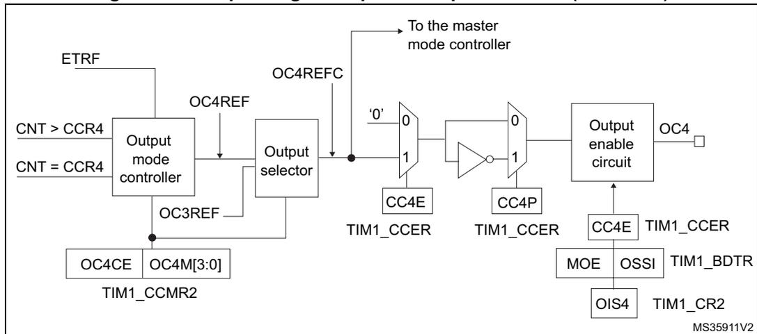
Figure 375. Output stage of capture/compare channel (channel 4)
The diagram illustrates the output stage for capture/compare channel 4. The signal flow starts with ETRF and CNT/CCR4 inputs to an 'Output mode controller'. This controller outputs OC4REF, which is then processed by an 'Output selector'. The 'Output selector' also receives OC3REF and OC4REFC signals. The 'Output selector' outputs OC4REFC to the master mode controller and OC4_DT and OC4N_DT signals to a 'Dead-time generator'. The 'Dead-time generator' is controlled by DTG[7:0] from TIM1_BDTR. The 'Dead-time generator' outputs OC4_DT and OC4N_DT signals to multiplexers. These multiplexers are controlled by '0', 'x0', '01', and '11' signals from CC4NE, CC4E, and CC4P registers in TIM1_CCER. The multiplexers output signals to an 'Output enable circuit' block, which produces OC4 output. The 'Output enable circuit' block is also controlled by CC4NE, MOE, OSSI, and OSSR signals from TIM1_BDTR and TIM1_CR2. Control registers shown include TIM1_CCMR2 (OC4CE, OC4M[3:0]), TIM1_BDTR (DTG[7:0], MOE, OSSI, OSSR), TIM1_CCER (CC4NE, CC4E, CC4P), and TIM1_CR2 (OIS4).
Figure 376. Output stage of capture/compare channel (channel 5, idem ch. 6)
![Figure 376. Output stage of capture/compare channel (channel 5, idem ch. 6). The diagram shows the internal logic of the output stage. It starts with an 'Output mode controller' block receiving inputs 'ETRF', 'CNT > CCR5', and 'CNT = CCR5'. This block is connected to 'TIM1_CCMR2' registers 'OC5CE' and 'OC5M[3:0]'. The controller outputs 'OC5REF' to a multiplexer. The multiplexer has inputs '0' and '1', with 'CC5E' from 'TIM1_CCER' as the select signal. The output of the multiplexer goes through an inverter and then to another multiplexer. This second multiplexer has inputs '0' and '1', with 'CC5P' from 'TIM1_CCER' as the select signal. The output of this multiplexer goes to an 'Output enable circuit' block. This block is connected to 'TIM1_CCMR2' register 'CC5E', 'TIM1_BDTR' registers 'MOE' and 'OSSI', and 'TIM1_CR2' register 'OIS5'. The final output is 'OC5' (1). A label 'MS35910V2' is in the bottom right corner.](/RM0433-STM32H742-743-753-750/7d0ac6ea89262a357430adadc7466671_img.jpg)
1. Not available externally.
The capture/compare block is made of one preload register and one shadow register. Write and read always access the preload register.
In capture mode, captures are actually done in the shadow register, which is copied into the preload register.
In compare mode, the content of the preload register is copied into the shadow register which is compared to the counter.
38.3.7 Input capture mode
In Input capture mode, the Capture/Compare Registers (TIMx_CCRx) are used to latch the value of the counter after a transition detected by the corresponding ICx signal. When a capture occurs, the corresponding CCxIF flag (TIMx_SR register) is set and an interrupt or a DMA request can be sent if they are enabled. If a capture occurs while the CCxIF flag was already high, then the over-capture flag CCxOF (TIMx_SR register) is set. CCxIF can be cleared by software by writing it to '0' or by reading the captured data stored in the TIMx_CCRx register. CCxOF is cleared when written with '0'.
The following example shows how to capture the counter value in TIMx_CCR1 when TI1 input rises. To do this, use the following procedure:
- 1. Select the proper TI1x source (internal or external) with the TI1SEL[3:0] bits in the TIMx_TISEL register.
- 2. Select the active input: TIMx_CCR1 must be linked to the TI1 input, so write the CC1S bits to 01 in the TIMx_CCMR1 register. As soon as CC1S becomes different from 00, the channel is configured in input and the TIMx_CCR1 register becomes read-only.
- 3. Program the appropriate input filter duration in relation with the signal connected to the timer (when the input is one of the TIx (ICxF bits in the TIMx_CCMRx register). Let's imagine that, when toggling, the input signal is not stable during at most 5 internal clock cycles. We must program a filter duration longer than these 5 clock cycles. We can validate a transition on TI1 when 8 consecutive samples with the new level have been
detected (sampled at \( f_{DTS} \) frequency). Then write IC1F bits to 0011 in the TIMx_CCMR1 register.
- 4. Select the edge of the active transition on the TI1 channel by writing CC1P and CC1NP bits to 0 in the TIMx_CCER register (rising edge in this case).
- 5. Program the input prescaler. In our example, we wish the capture to be performed at each valid transition, so the prescaler is disabled (write IC1PS bits to '00' in the TIMx_CCMR1 register).
- 6. Enable capture from the counter into the capture register by setting the CC1E bit in the TIMx_CCER register.
- 7. If needed, enable the related interrupt request by setting the CC1IE bit in the TIMx_DIER register, and/or the DMA request by setting the CC1DE bit in the TIMx_DIER register.
When an input capture occurs:
- • The TIMx_CCR1 register gets the value of the counter on the active transition.
- • CC1IF flag is set (interrupt flag). CC1OF is also set if at least two consecutive captures occurred whereas the flag was not cleared.
- • An interrupt is generated depending on the CC1IE bit.
- • A DMA request is generated depending on the CC1DE bit.
In order to handle the overcapture, it is recommended to read the data before the overcapture flag. This is to avoid missing an overcapture which could happen after reading the flag and before reading the data.
Note: IC interrupt and/or DMA requests can be generated by software by setting the corresponding CCxG bit in the TIMx_EGR register.
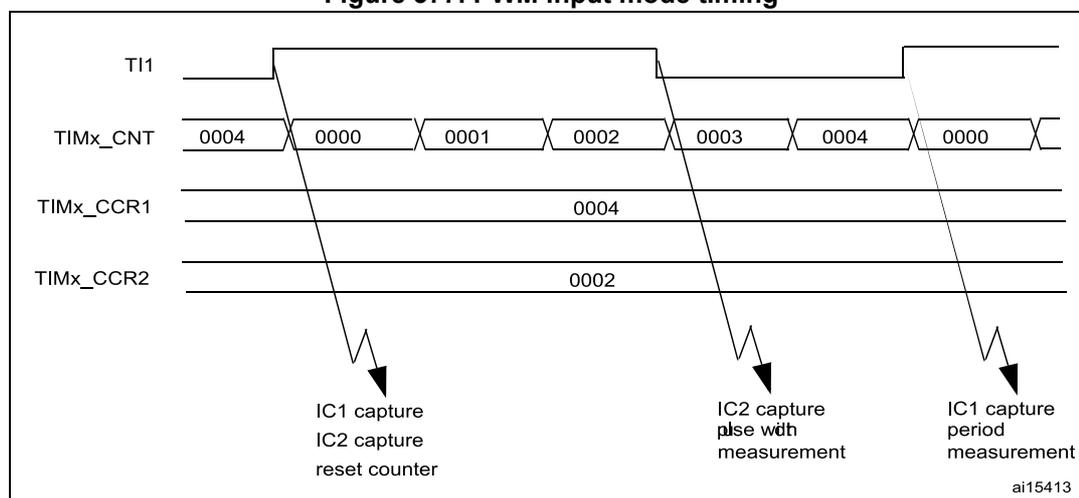
38.3.8 PWM input mode
This mode is a particular case of input capture mode. The procedure is the same except:
- • Two ICx signals are mapped on the same TIx input.
- • These 2 ICx signals are active on edges with opposite polarity.
- • One of the two TIxFP signals is selected as trigger input and the slave mode controller is configured in reset mode.
For example, the user can measure the period (in TIMx_CCR1 register) and the duty cycle (in TIMx_CCR2 register) of the PWM applied on TI1 using the following procedure (depending on CK_INT frequency and prescaler value):
- 1. Select the proper TI1x source (internal or external) with the TI1SEL[3:0] bits in the TIMx_TISEL register.
- 2. Select the active input for TIMx_CCR1: write the CC1S bits to 01 in the TIMx_CCMR1 register (TI1 selected).
- 3. Select the active polarity for TI1FP1 (used both for capture in TIMx_CCR1 and counter clear): write the CC1P and CC1NP bits to '0' (active on rising edge).
- 4. Select the active input for TIMx_CCR2: write the CC2S bits to 10 in the TIMx_CCMR1 register (TI1 selected).
- 5. Select the active polarity for TI1FP2 (used for capture in TIMx_CCR2): write the CC2P and CC2NP bits to CC2P/CC2NP='10' (active on falling edge).
- 6. Select the valid trigger input: write the TS bits to 00101 in the TIMx_SMCR register (TI1FP1 selected).
- 7. Configure the slave mode controller in reset mode: write the SMS bits to 0100 in the TIMx_SMCR register.
- 8. Enable the captures: write the CC1E and CC2E bits to '1' in the TIMx_CCER register.
Figure 377. PWM input mode timing
38.3.9 Forced output mode
In output mode (CCxS bits = 00 in the TIMx_CCMRx register), each output compare signal (OCxREF and then OCx/OCxN) can be forced to active or inactive level directly by software, independently of any comparison between the output compare register and the counter.
To force an output compare signal (OCxREF/OCx) to its active level, user just needs to write 0101 in the OCxM bits in the corresponding TIMx_CCMRx register. Thus OCxREF is forced high (OCxREF is always active high) and OCx get opposite value to CCxP polarity bit.
For example: CCxP=0 (OCx active high) => OCx is forced to high level.
The OCxREF signal can be forced low by writing the OCxM bits to 0100 in the TIMx_CCMRx register.
Anyway, the comparison between the TIMx_CCRx shadow register and the counter is still performed and allows the flag to be set. Interrupt and DMA requests can be sent accordingly. This is described in the output compare mode section below.
38.3.10 Output compare mode
This function is used to control an output waveform or indicate when a period of time has elapsed. Channels 1 to 4 can be output, while Channel 5 and 6 are only available inside the device (for instance, for compound waveform generation or for ADC triggering).
When a match is found between the capture/compare register and the counter, the output compare function:
- • Assigns the corresponding output pin to a programmable value defined by the output compare mode (OCxM bits in the TIMx_CCMRx register) and the output polarity (CCxP bit in the TIMx_CCER register). The output pin can keep its level (OCXM=0000), be set active (OCxM=0001), be set inactive (OCxM=0010) or can toggle (OCxM=0011) on match.
- • Sets a flag in the interrupt status register (CCxIF bit in the TIMx_SR register).
- • Generates an interrupt if the corresponding interrupt mask is set (CCxIE bit in the TIMx_DIER register).
- • Sends a DMA request if the corresponding enable bit is set (CCxDE bit in the TIMx_DIER register, CCDS bit in the TIMx_CR2 register for the DMA request selection).
The TIMx_CCRx registers can be programmed with or without preload registers using the OCxPE bit in the TIMx_CCMRx register.
In output compare mode, the update event UEV has no effect on OCxREF and OCx output. The timing resolution is one count of the counter. Output compare mode can also be used to output a single pulse (in One Pulse mode).
Procedure
- 1. Select the counter clock (internal, external, prescaler).
- 2. Write the desired data in the TIMx_ARR and TIMx_CCRx registers.
- 3. Set the CCxIE bit if an interrupt request is to be generated.
- 4. Select the output mode. For example:
- – Write OCxM = 0011 to toggle OCx output pin when CNT matches CCRx
- – Write OCxPE = 0 to disable preload register
- – Write CCxP = 0 to select active high polarity
- – Write CCxE = 1 to enable the output
- 5. Enable the counter by setting the CEN bit in the TIMx_CR1 register.
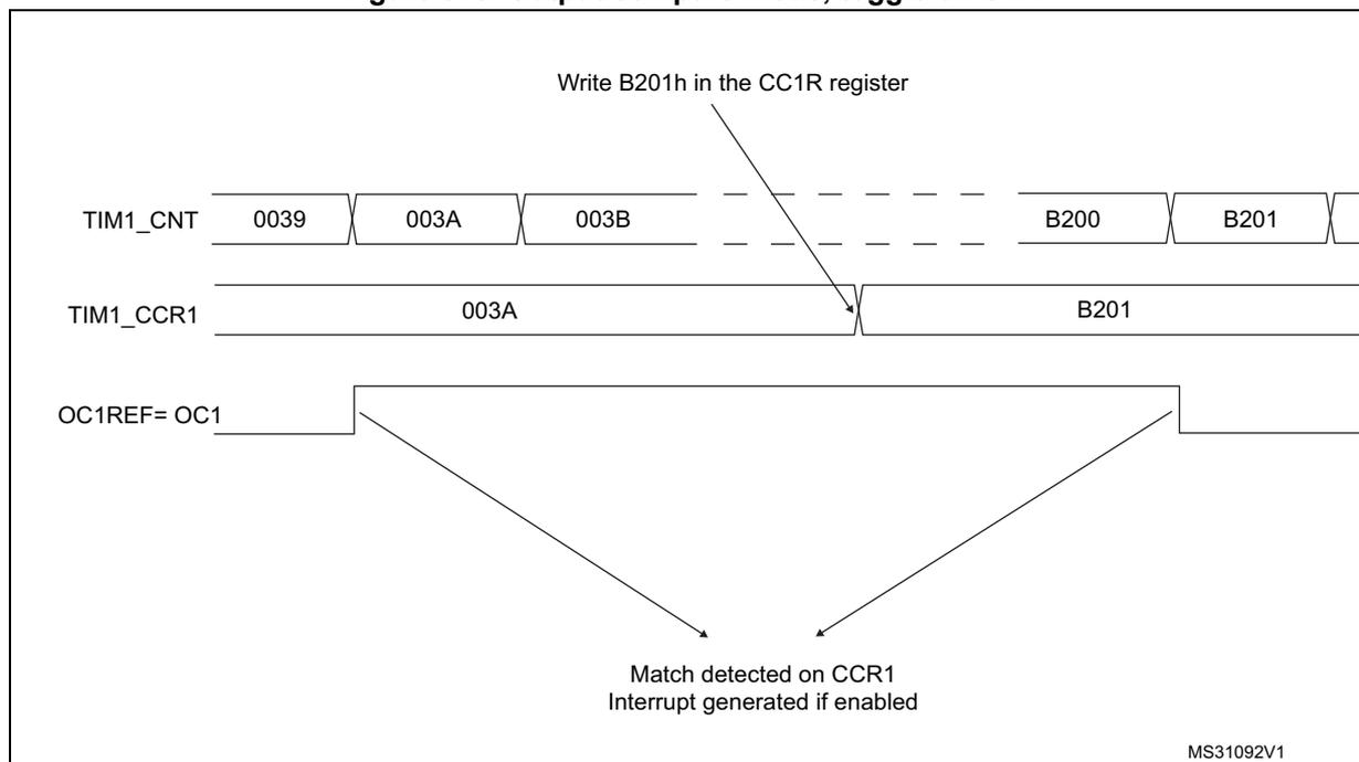
The TIMx_CCRx register can be updated at any time by software to control the output waveform, provided that the preload register is not enabled (OCxPE='0', else TIMx_CCRx shadow register is updated only at the next update event UEV). An example is given in Figure 378 .
Figure 378. Output compare mode, toggle on OC1
38.3.11 PWM mode
Pulse Width Modulation mode allows a signal to be generated with a frequency determined by the value of the TIMx_ARR register and a duty cycle determined by the value of the TIMx_CCRx register.
The PWM mode can be selected independently on each channel (one PWM per OCx output) by writing '0110' (PWM mode 1) or '0111' (PWM mode 2) in the OCxM bits in the TIMx_CCMRx register. The corresponding preload register must be enabled by setting the OCxPE bit in the TIMx_CCMRx register, and eventually the auto-reload preload register (in upcounting or center-aligned modes) by setting the ARPE bit in the TIMx_CR1 register.
As the preload registers are transferred to the shadow registers only when an update event occurs, before starting the counter, all registers must be initialized by setting the UG bit in the TIMx_EGR register.
OCx polarity is software programmable using the CCxP bit in the TIMx_CCER register. It can be programmed as active high or active low. OCx output is enabled by a combination of the CCxE, CCxNE, MOE, OSSI and OSSR bits (TIMx_CCER and TIMx_BDTR registers). Refer to the TIMx_CCER register description for more details.
In PWM mode (1 or 2), TIMx_CNT and TIMx_CCRx are always compared to determine whether \( TIMx\_CCRx \leq TIMx\_CNT \) or \( TIMx\_CNT \leq TIMx\_CCRx \) (depending on the direction of the counter).
The timer is able to generate PWM in edge-aligned mode or center-aligned mode depending on the CMS bits in the TIMx_CR1 register.
PWM edge-aligned mode
- • Upcounting configuration
Upcounting is active when the DIR bit in the TIMx_CR1 register is low. Refer to the Upcounting mode on page 1531 .
In the following example, we consider PWM mode 1. The reference PWM signal OCxREF is high as long as TIMx_CNT < TIMx_CCRx else it becomes low. If the compare value in TIMx_CCRx is greater than the auto-reload value (in TIMx_ARR) then OCxREF is held at '1'. If the compare value is 0 then OCxRef is held at '0'.
Figure 379 shows some edge-aligned PWM waveforms in an example where TIMx_ARR=8.
Figure 379. Edge-aligned PWM waveforms (ARR=8)
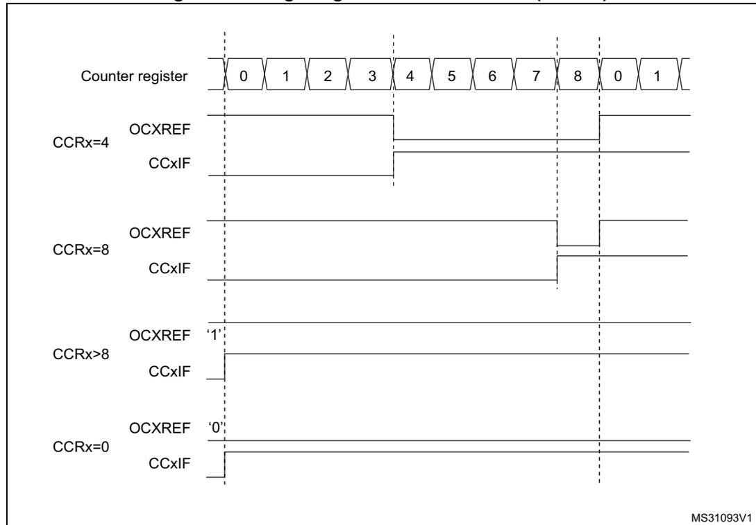
The figure is a timing diagram illustrating edge-aligned PWM waveforms for different compare register (CCR) values. The counter register (TIMx_CNT) counts from 0 to 8 and then reloads to 0. The diagram shows four cases: CCRx=4, CCRx=8, CCRx>8, and CCRx=0. For each case, the OCxREF signal and the CCxIF flag are shown. Vertical dashed lines indicate the counter values 0, 4, 8, and the reload point. MS31093V1 is noted in the bottom right.
| Counter register | 0 | 1 | 2 | 3 | 4 | 5 | 6 | 7 | 8 | 0 | 1 | |
|---|---|---|---|---|---|---|---|---|---|---|---|---|
| CCRx=4 | OCxREF: High | OCxREF: Low | OCxREF: High | |||||||||
| CCxIF | Low | High | Low | |||||||||
| CCRx=8 | OCxREF: High | OCxREF: Low | ||||||||||
| CCxIF | Low | High | ||||||||||
| CCRx>8 | OCxREF: High | |||||||||||
| CCxIF | Low | |||||||||||
| CCRx=0 | OCxREF: Low | |||||||||||
| CCxIF | High | |||||||||||
- • Downcounting configuration
Downcounting is active when DIR bit in TIMx_CR1 register is high. Refer to the Downcounting mode on page 1535
In PWM mode 1, the reference signal OCxRef is low as long as TIMx_CNT > TIMx_CCRx else it becomes high. If the compare value in TIMx_CCRx is greater than the auto-reload value in TIMx_ARR, then OCxREF is held at '1'. 0% PWM is not possible in this mode.
PWM center-aligned mode
Center-aligned mode is active when the CMS bits in TIMx_CR1 register are different from '00' (all the remaining configurations having the same effect on the OCxRef/OCx signals). The compare flag is set when the counter counts up, when it counts down or both when it counts up and down depending on the CMS bits configuration. The direction bit (DIR) in the
TIMx_CR1 register is updated by hardware and must not be changed by software. Refer to the Center-aligned mode (up/down counting) on page 1538 .
Figure 380 shows some center-aligned PWM waveforms in an example where:
- • TIMx_ARR=8,
- • PWM mode is the PWM mode 1,
- • The flag is set when the counter counts down corresponding to the center-aligned mode 1 selected for CMS=01 in TIMx_CR1 register.
Figure 380. Center-aligned PWM waveforms (ARR=8)
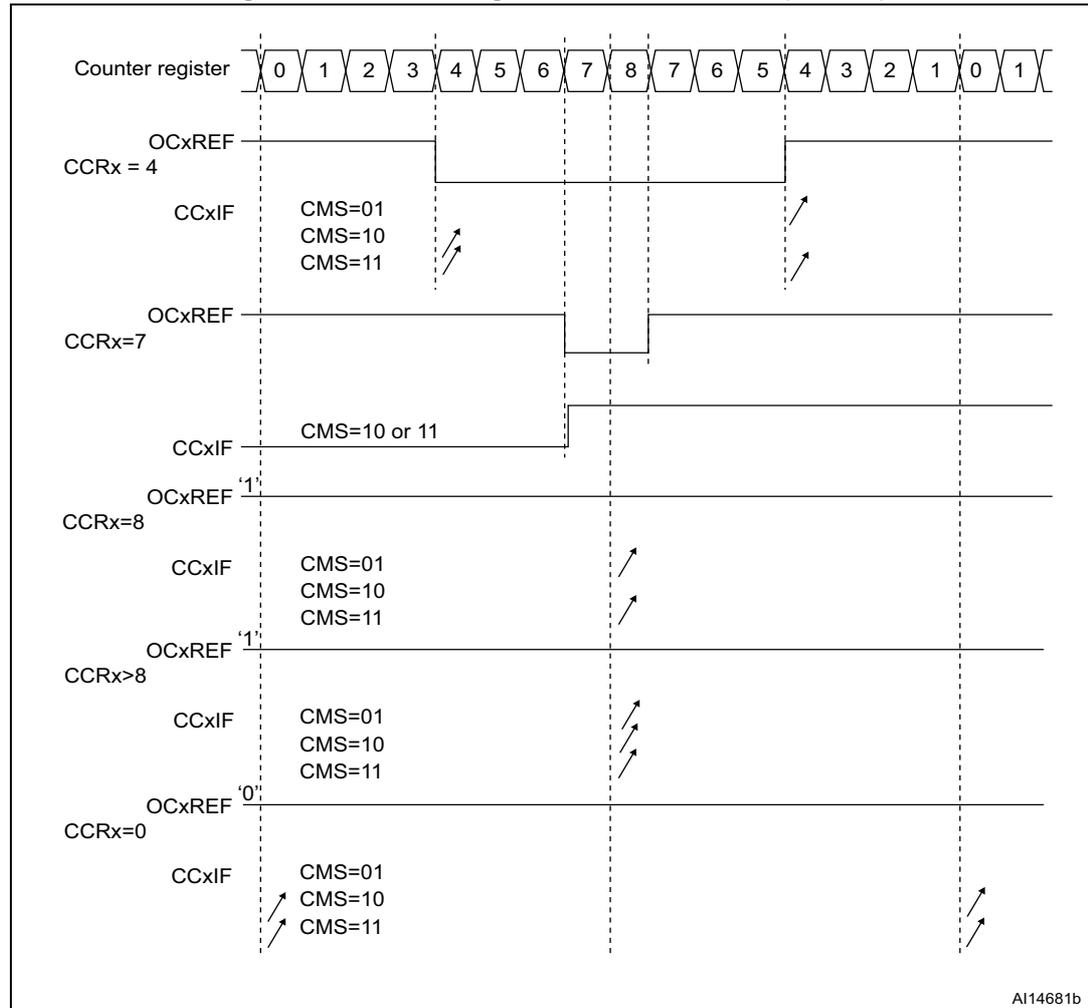
The figure illustrates the relationship between the counter register values and the resulting PWM waveforms for different capture/compare register (CCR) values. The counter register values are shown at the top, ranging from 0 to 8 and then back down to 0, with an additional '1' at the end: 0, 1, 2, 3, 4, 5, 6, 7, 8, 7, 6, 5, 4, 3, 2, 1, 0, 1. Vertical dashed lines indicate the points where the counter reaches the CCRx values.
- CCRx = 4: The OCxREF signal is high from counter 0 to 4 (upcounting) and high from 4 to 0 (downcounting). It is low between counter 4 and 8. The CCxIF flag is set when the counter counts down and reaches 4. CMS settings shown: CMS=01, CMS=10, CMS=11.
- CCRx = 7: The OCxREF signal is high from counter 0 to 7 and low from 7 to 8. The CCxIF flag is set when the counter counts down and reaches 7. CMS settings shown: CMS=10 or 11.
- CCRx = 8: The OCxREF signal is high ('1') throughout the cycle. The CCxIF flag is set when the counter reaches 8 (the peak). CMS settings shown: CMS=01, CMS=10, CMS=11.
- CCRx > 8: The OCxREF signal is high ('1') throughout the cycle. The CCxIF flag is set when the counter reaches 8. CMS settings shown: CMS=01, CMS=10, CMS=11.
- CCRx = 0: The OCxREF signal is low ('0') throughout the cycle. The CCxIF flag is set when the counter reaches 0. CMS settings shown: CMS=01, CMS=10, CMS=11.
Arrows indicate the direction of the counter (up or down) and the resulting flag setting. The label AI14681b is present in the bottom right corner.
Hints on using center-aligned mode
- • When starting in center-aligned mode, the current up-down configuration is used. It means that the counter counts up or down depending on the value written in the DIR bit
in the TIMx_CR1 register. Moreover, the DIR and CMS bits must not be changed at the same time by the software.
- • Writing to the counter while running in center-aligned mode is not recommended as it can lead to unexpected results. In particular:
- – The direction is not updated if a value greater than the auto-reload value is written in the counter (TIMx_CNT > TIMx_ARR). For example, if the counter was counting up, it continues to count up.
- – The direction is updated if 0 or the TIMx_ARR value is written in the counter but no Update Event UEV is generated.
- • The safest way to use center-aligned mode is to generate an update by software (setting the UG bit in the TIMx_EGR register) just before starting the counter and not to write the counter while it is running.
38.3.12 Asymmetric PWM mode
Asymmetric mode allows two center-aligned PWM signals to be generated with a programmable phase shift. While the frequency is determined by the value of the TIMx_ARR register, the duty cycle and the phase-shift are determined by a pair of TIMx_CCRx register. One register controls the PWM during up-counting, the second during down counting, so that PWM is adjusted every half PWM cycle:
- – OC1REFC (or OC2REFC) is controlled by TIMx_CCR1 and TIMx_CCR2
- – OC3REFC (or OC4REFC) is controlled by TIMx_CCR3 and TIMx_CCR4
Asymmetric PWM mode can be selected independently on two channel (one OCx output per pair of CCR registers) by writing '1110' (Asymmetric PWM mode 1) or '1111' (Asymmetric PWM mode 2) in the OCxM bits in the TIMx_CCMRx register.
Note: The OCxM[3:0] bit field is split into two parts for compatibility reasons, the most significant bit is not contiguous with the 3 least significant ones.
When a given channel is used as asymmetric PWM channel, its complementary channel can also be used. For instance, if an OC1REFC signal is generated on channel 1 (Asymmetric PWM mode 1), it is possible to output either the OC2REF signal on channel 2, or an OC2REFC signal resulting from asymmetric PWM mode 1.
Figure 381 represents an example of signals that can be generated using Asymmetric PWM mode (channels 1 to 4 are configured in Asymmetric PWM mode 1). Together with the deadtime generator, this allows a full-bridge phase-shifted DC to DC converter to be controlled.
Figure 381. Generation of 2 phase-shifted PWM signals with 50% duty cycle
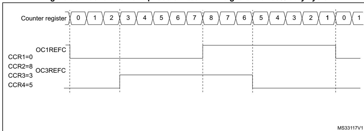
The figure shows a timing diagram for two phase-shifted PWM signals. The top row represents the 'Counter register' values: 0, 1, 2, 3, 4, 5, 6, 7, 8, 7, 6, 5, 4, 3, 2, 1, 0, 1. Vertical dashed lines mark the counter values 0, 3, 5, 8, and 0 again. Below the counter, two PWM signals are shown:
- OC1REFC : Controlled by CCR1=0 and CCR2=8. It is high from counter value 0 to 8 and low from 8 back to 0.
- OC3REFC : Controlled by CCR3=3 and CCR4=5. It is high from counter value 3 to 5 and low from 5 back to 3.
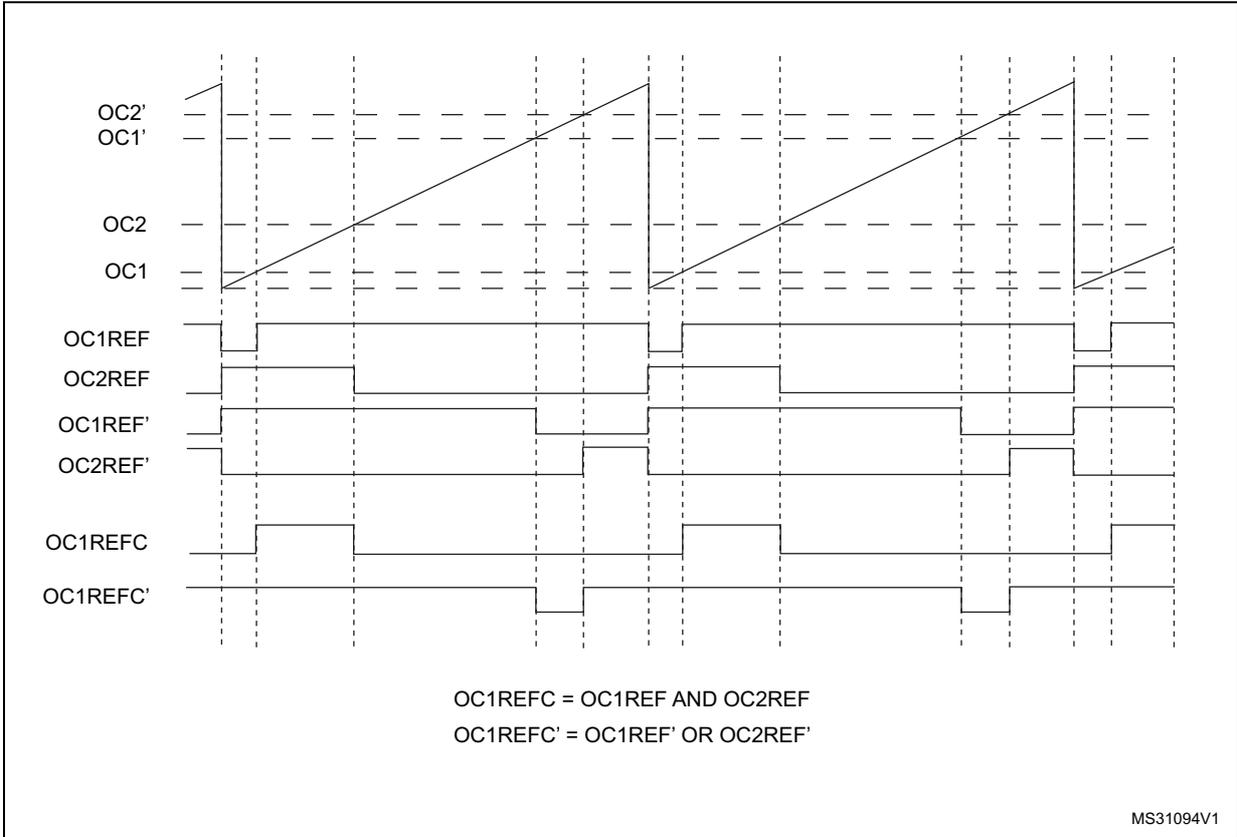
38.3.13 Combined PWM mode
Combined PWM mode allows two edge or center-aligned PWM signals to be generated with programmable delay and phase shift between respective pulses. While the frequency is determined by the value of the TIMx_ARR register, the duty cycle and delay are determined by the two TIMx_CCRx registers. The resulting signals, OCxREFC, are made of an OR or AND logical combination of two reference PWMs:
- – OC1REFC (or OC2REFC) is controlled by TIMx_CCR1 and TIMx_CCR2
- – OC3REFC (or OC4REFC) is controlled by TIMx_CCR3 and TIMx_CCR4
Combined PWM mode can be selected independently on two channels (one OCx output per pair of CCR registers) by writing '1100' (Combined PWM mode 1) or '1101' (Combined PWM mode 2) in the OCxM bits in the TIMx_CCMRx register.
When a given channel is used as combined PWM channel, its complementary channel must be configured in the opposite PWM mode (for instance, one in Combined PWM mode 1 and the other in Combined PWM mode 2).
Note: The OCxM[3:0] bit field is split into two parts for compatibility reasons, the most significant bit is not contiguous with the 3 least significant ones.
Figure 382 represents an example of signals that can be generated using Asymmetric PWM mode, obtained with the following configuration:
- – Channel 1 is configured in Combined PWM mode 2,
- – Channel 2 is configured in PWM mode 1,
- – Channel 3 is configured in Combined PWM mode 2,
- – Channel 4 is configured in PWM mode 1.
Figure 382. Combined PWM mode on channel 1 and 3
MS31094V1
38.3.14 Combined 3-phase PWM mode
Combined 3-phase PWM mode allows one to three center-aligned PWM signals to be generated with a single programmable signal ANDed in the middle of the pulses. The OC5REF signal is used to define the resulting combined signal. The 3-bits GC5C[3:1] in the TIMx_CCR5 allow selection on which reference signal the OC5REF is combined. The resulting signals, OCxREFC, are made of an AND logical combination of two reference PWMs:
- – If GC5C1 is set, OC1REFC is controlled by TIMx_CCR1 and TIMx_CCR5
- – If GC5C2 is set, OC2REFC is controlled by TIMx_CCR2 and TIMx_CCR5
- – If GC5C3 is set, OC3REFC is controlled by TIMx_CCR3 and TIMx_CCR5
Combined 3-phase PWM mode can be selected independently on channels 1 to 3 by setting at least one of the 3-bits GC5C[3:1].
Figure 383. 3-phase combined PWM signals with multiple trigger pulses per period
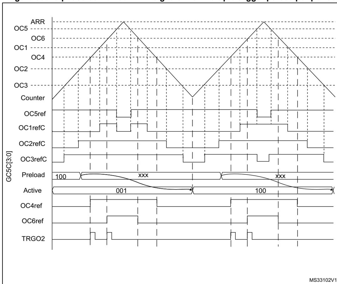
The TRGO2 waveform shows how the ADC can be synchronized on given 3-phase PWM signals. Refer to Section 38.3.27: ADC synchronization for more details.
38.3.15 Complementary outputs and dead-time insertion
The advanced-control timers (TIM1/TIM8) can output two complementary signals and manage the switching-off and the switching-on instants of the outputs.
This time is generally known as dead-time and it has to be adjusted depending on the devices that are connected to the outputs and their characteristics (intrinsic delays of level-shifters, delays due to power switches...)
The polarity of the outputs (main output OCx or complementary OCxN) can be selected independently for each output. This is done by writing to the CCxP and CCxNP bits in the TIMx_CCER register.
The complementary signals OCx and OCxN are activated by a combination of several control bits: the CCxE and CCxNE bits in the TIMx_CCER register and the MOE, OISx, OISxN, OSSI and OSSR bits in the TIMx_BDTR and TIMx_CR2 registers. Refer to Table 334: Output control bits for complementary OCx and OCxN channels with break feature on page 1606 for more details. In particular, the dead-time is activated when switching to the idle state (MOE falling down to 0).
Dead-time insertion is enabled by setting both CCxE and CCxNE bits, and the MOE bit if the break circuit is present. There is one 10-bit dead-time generator for each channel. From a reference waveform OCxREF, it generates 2 outputs OCx and OCxN. If OCx and OCxN are active high:
- • The OCx output signal is the same as the reference signal except for the rising edge, which is delayed relative to the reference rising edge.
- • The OCxN output signal is the opposite of the reference signal except for the rising edge, which is delayed relative to the reference falling edge.
If the delay is greater than the width of the active output (OCx or OCxN) then the corresponding pulse is not generated.
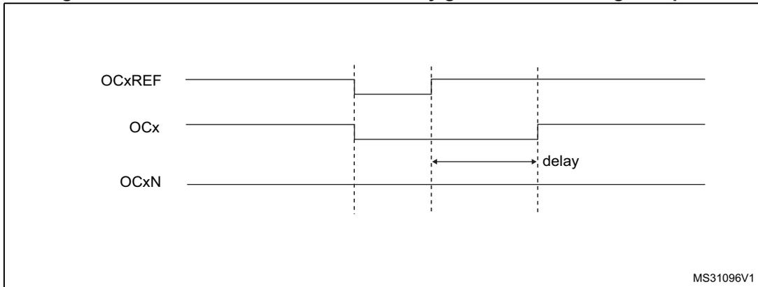
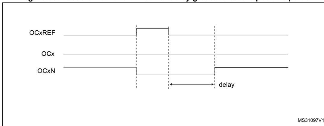
The following figures show the relationships between the output signals of the dead-time generator and the reference signal OCxREF. (we suppose CCxP=0, CCxNP=0, MOE=1, CCxE=1 and CCxNE=1 in these examples)
Figure 384. Complementary output with dead-time insertion
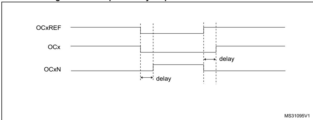
Timing diagram showing three waveforms: OCxREF, OCx, and OCxN. OCxREF is a square wave. OCx is the inverted OCxREF signal with a delay on its rising edge. OCxN is the OCxREF signal with a delay on its rising edge. The delay is indicated by double-headed arrows between the rising edges of the reference and the outputs. MS31095V1
Figure 385. Dead-time waveforms with delay greater than the negative pulse
Timing diagram showing three waveforms: OCxREF, OCx, and OCxN. OCxREF is a square wave. OCx is the inverted OCxREF signal with a delay on its rising edge. OCxN is the OCxREF signal with a delay on its rising edge. The delay is indicated by a double-headed arrow between the rising edges of the reference and the outputs. MS31096V1
Figure 386. Dead-time waveforms with delay greater than the positive pulse
The dead-time delay is the same for each of the channels and is programmable with the DTG bits in the TIMx_BDTR register. Refer to Section 38.4.20: TIMx break and dead-time register (TIMx_BDTR)(x = 1, 8) for delay calculation.
Re-directing OCxREF to OCx or OCxN
In output mode (forced, output compare or PWM), OCxREF can be re-directed to the OCx output or to OCxN output by configuring the CCxE and CCxNE bits in the TIMx_CCER register.
This allows a specific waveform to be sent (such as PWM or static active level) on one output while the complementary remains at its inactive level. Other alternative possibilities are to have both outputs at inactive level or both outputs active and complementary with dead-time.
Note: When only OCxN is enabled (CCxE=0, CCxNE=1), it is not complemented and becomes active as soon as OCxREF is high. For example, if CCxNP=0 then OCxN=OCxRef. On the other hand, when both OCx and OCxN are enabled (CCxE=CCxNE=1) OCx becomes active when OCxREF is high whereas OCxN is complemented and becomes active when OCxREF is low.
38.3.16 Using the break function
The purpose of the break function is to protect power switches driven by PWM signals generated with the TIM1 and TIM8 timers. The two break inputs are usually connected to fault outputs of power stages and 3-phase inverters. When activated, the break circuitry shuts down the PWM outputs and forces them to a predefined safe state. A number of internal MCU events can also be selected to trigger an output shut-down.
The break features two channels. A break channel which gathers both system-level fault (clock failure, parity error,...) and application fault (from input pins and built-in comparator), and can force the outputs to a predefined level (either active or inactive) after a deadtime duration. A break2 channel which only includes application faults and is able to force the outputs to an inactive state.
The output enable signal and output levels during break are depending on several control bits:
- – the MOE bit in TIMx_BDTR register allows the outputs to be enabled/disabled by software and is reset in case of break or break2 event.
- – the OSSI bit in the TIMx_BDTR register defines whether the timer controls the output in inactive state or releases the control to the GPIO controller (typically to have it in Hi-Z mode)
- – the OISx and OISxN bits in the TIMx_CR2 register which are setting the output shut-down level, either active or inactive. The OCx and OCxN outputs cannot be set both to active level at a given time, whatever the OISx and OISxN values.
Refer to Table 334: Output control bits for complementary OCx and OCxN channels with break feature on page 1606 for more details.
When exiting from reset, the break circuit is disabled and the MOE bit is low. The break functions can be enabled by setting the BKE and BK2E bits in the TIMx_BDTR register. The break input polarities can be selected by configuring the BKP and BK2P bits in the same register. BKE/BK2E and BKP/BK2P can be modified at the same time. When the BKE/BK2E and BKP/BK2P bits are written, a delay of 1 APB clock cycle is applied before the writing is effective. Consequently, it is necessary to wait 1 APB clock period to correctly read back the bit after the write operation.
Because MOE falling edge can be asynchronous, a resynchronization circuit has been inserted between the actual signal (acting on the outputs) and the synchronous control bit (accessed in the TIMx_BDTR register). It results in some delays between the asynchronous and the synchronous signals. In particular, if MOE is set to 1 whereas it was low, a delay must be inserted (dummy instruction) before reading it correctly. This is because the write acts on the asynchronous signal whereas the read reflects the synchronous signal.
The sources for break (BRK) channel are:
- • An external source connected to one of the BKIN pin (as per selection done in the GPIO alternate function registers), with polarity selection and optional digital filtering
- • An internal source:
- – the output from a comparator, with polarity selection and optional digital filtering
- – the analog watchdog output of the DFSDM1 peripheral
- – A system break:
- - the Cortex ® -M7 LOCKUP output
- - the PVD output
- - all SRAM and TCM ECC dual error detections (AXI-SRAM, ITCM, DTCM, SRAM1, SRAM2, SRAM3, SRAM4, BKRAM, refer to SYSCFG_CFGR register for details)
- - a flash memory ECC dual error detection
- - a clock failure event generated by the CSS detector
The sources for break2 (BRK2) are:
- • An external source connected to one of the BKIN pin (as per selection done in the GPIO alternate function registers), with polarity selection and optional digital filtering
- • An internal source coming from a comparator output.
- • The analog watchdog output of the DFSDM1 peripheral
Break events can also be generated by software using BG and B2G bits in the TIMx_EGR register. The software break generation using BG and B2G is active whatever the BKE and BK2E enable bits values.
All sources are ORed before entering the timer BRK or BRK2 inputs, as per Figure 387 below.
Figure 387. Break and Break2 circuitry overview
![Figure 387. Break and Break2 circuitry overview. This block diagram illustrates the logic for generating break and break2 signals in advanced-control timers. It is divided into two main sections: System break requests and Application break requests. System break requests are generated by an OR gate combining Lockup LOCK, PVD LOCK, Parity LOCK, ECC LOCK, and CSS signals, leading to the SBIF flag. Application break requests are generated by two parallel paths for BRK and BRK2. Each path includes an OR gate for BKIN, BKCMP, and BKDFBKxE inputs, followed by a filter (BKF[3:0] or BK2F[3:0]), an inverter (BKP or BK2P), and a final OR gate with software break requests (BG or B2G) and enable bits (BKE or BK2E) to produce the BRK or BRK2 request and the corresponding BIF or B2IF flag.](/RM0433-STM32H742-743-753-750/c1ea15990434b79b0a6ee6fc0aa3602c_img.jpg)
The diagram shows the circuitry for generating break and break2 signals. At the top, five signals (Lockup LOCK, PVD LOCK, Parity LOCK, ECC LOCK, and CSS) are ORed together to produce 'System break requests', which set the SBIF flag. Below this, the 'Application break requests' section is split into two identical paths for BRK and BRK2. Each path starts with an OR gate combining BKIN (from AF controller via BKINP), BKCMP (from COMP1 and COMP2 outputs via BKCMP1P/2P), and BKDFBKxE (from DFSDM BREAK output) inputs. This is followed by a filter block (BKF[3:0] or BK2F[3:0]), an inverter (BKP or BK2P), and a final OR gate that also takes 'Software break requests' (BG or B2G) and enable bits (BKE or BK2E) as inputs. The output of this final OR gate is the BRK or BRK2 request, which also sets the BIF or B2IF flag. The diagram is labeled MSv63016V1 in the bottom right corner.
Note: An asynchronous (clockless) operation is only guaranteed when the programmable filter is disabled. If it is enabled, a fail safe clock mode (for example by using the internal PLL and/or the CSS) must be used to guarantee that break events are handled.
When one of the breaks occurs (selected level on one of the break inputs):
- • The MOE bit is cleared asynchronously, putting the outputs in inactive state, idle state or even releasing the control to the GPIO controller (selected by the OSSI bit). This feature is enabled even if the MCU oscillator is off.
- • Each output channel is driven with the level programmed in the OISx bit in the TIMx_CR2 register as soon as MOE=0. If OSSI=0, the timer releases the output control (taken over by the GPIO controller), otherwise the enable output remains high.
- • When complementary outputs are used:
- – The outputs are first put in inactive state (depending on the polarity). This is done asynchronously so that it works even if no clock is provided to the timer.
- – If the timer clock is still present, then the dead-time generator is reactivated in order to drive the outputs with the level programmed in the OISx and OISxN bits after a dead-time. Even in this case, OCx and OCxN cannot be driven to their active level together. Note that because of the resynchronization on MOE, the dead-time duration is slightly longer than usual (around 2 ck_tim clock cycles).
- – If OSSI=0, the timer releases the output control (taken over by the GPIO controller which forces a Hi-Z state), otherwise the enable outputs remain or become high as soon as one of the CCxE or CCxNE bits is high.
- • The break status flag (SBIF, BIF and B2IF bits in the TIMx_SR register) is set. An interrupt is generated if the BIE bit in the TIMx_DIER register is set.
- • If the AOE bit in the TIMx_BDTR register is set, the MOE bit is automatically set again at the next update event (UEV). As an example, this can be used to perform a regulation. Otherwise, MOE remains low until the application sets it to '1' again. In this case, it can be used for security and the break input can be connected to an alarm from power drivers, thermal sensors or any security components.
Note:
If the MOE is reset by the CPU while the AOE bit is set, the outputs are in idle state and forced to inactive level or Hi-Z depending on OSSI value.
If both the MOE and AOE bits are reset by the CPU, the outputs are in disabled state and driven with the level programmed in the OISx bit in the TIMx_CR2 register.
Note: The break inputs are active on level. Thus, the MOE cannot be set while the break input is active (neither automatically nor by software). In the meantime, the status flag BIF and B2IF cannot be cleared.
In addition to the break input and the output management, a write protection has been implemented inside the break circuit to safeguard the application. It allows the configuration of several parameters to be freeze (dead-time duration, OCx/OCxN polarities and state when disabled, OCxM configurations, break enable and polarity). The application can choose from 3 levels of protection selected by the LOCK bits in the TIMx_BDTR register. Refer to Section 38.4.20: TIMx break and dead-time register (TIMx_BDTR)(x = 1, 8) . The LOCK bits can be written only once after an MCU reset.
Figure 388 shows an example of behavior of the outputs in response to a break.
Figure 388. Various output behavior in response to a break event on BRK (OSSI = 1)
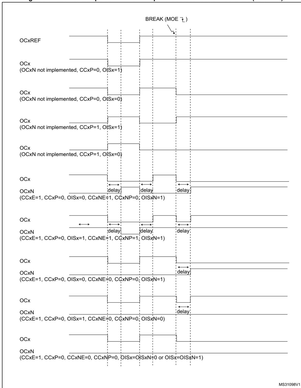
The diagram illustrates the output behavior of various timer channels (OCxREF, OCx, OCxN) in response to a break event (BREAK (MOE ↓)). The break event is indicated by a downward arrow at the top center. The outputs are shown as horizontal lines with transitions at the break event. The initial state of the outputs before the break event is determined by the configuration parameters listed below each output label. The 'delay' parameter indicates the time interval between the break event and the output transition.
- OCxREF : Output reference signal.
- OCx (OCxN not implemented, CCxP=0, OISx=1): Output x, active high, no inversion.
- OCx (OCxN not implemented, CCxP=0, OISx=0): Output x, active low, no inversion.
- OCx (OCxN not implemented, CCxP=1, OISx=1): Output x, active high, inversion.
- OCx (OCxN not implemented, CCxP=1, OISx=0): Output x, active low, inversion.
- OCx : Output x, state before break event.
- OCxN (CCxE=1, CCxP=0, OISx=0, CCxNE=1, CCxNP=0, OISxN=1): Output xN, active low, no inversion, inverted output active high.
- OCx : Output x, state before break event.
- OCxN (CCxE=1, CCxP=0, OISx=1, CCxNE=1, CCxNP=1, OISxN=1): Output xN, active low, inversion, inverted output active high.
- OCx : Output x, state before break event.
- OCxN (CCxE=1, CCxP=0, OISx=0, CCxNE=0, CCxNP=0, OISxN=1): Output xN, active low, no inversion, inverted output active low.
- OCx : Output x, state before break event.
- OCxN (CCxE=1, CCxP=0, OISx=1, CCxNE=0, CCxNP=0, OISxN=0): Output xN, active low, inversion, inverted output active low.
- OCx : Output x, state before break event.
- OCxN (CCxE=1, CCxP=0, CCxNE=0, CCxNP=0, OISx=OISxN=0 or OISx=OISxN=1): Output xN, active low, no inversion, inverted output active low.
MS31098V1
The two break inputs have different behaviors on timer outputs:
- – The BRK input can either disable (inactive state) or force the PWM outputs to a predefined safe state.
- – BRK2 can only disable (inactive state) the PWM outputs.
The BRK has a higher priority than BRK2 input, as described in Table 331 .
Note: BRK2 must only be used with OSSR = OSSI = 1.
Table 331. Behavior of timer outputs versus BRK/BRK2 inputs
| BRK | BRK2 | Timer outputs state | Typical use case | |
|---|---|---|---|---|
| OCxN output (low side switches) | OCx output (high side switches) | |||
| Active | X |
| ON after deadtime insertion | OFF |
| Inactive | Active | Inactive | OFF | OFF |
Figure 389 gives an example of OCx and OCxN output behavior in case of active signals on BRK and BRK2 inputs. In this case, both outputs have active high polarities (CCxP = CCxNP = 0 in TIMx_CCER register).
Figure 389. PWM output state following BRK and BRK2 pins assertion (OSSI=1)
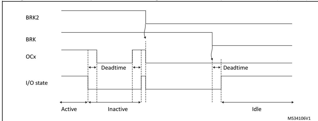
Figure 390. PWM output state following BRK assertion (OSSI=0)
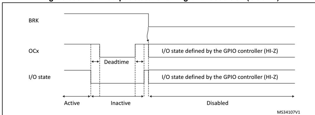
38.3.17 Bidirectional break inputs
Beside regular digital break inputs and internal break events coming from the comparators, the timer 1 and 8 are featuring bidirectional break inputs/outputs combining the two sources, as represented on Figure 391.
The TIMx_BKINy_COMPz pins are combining the COMPz output (to be configured in open drain) and the Timerx's TIMx_BKINy input. They allow to have:
- - A global break information available for external MCUs or gate drivers shut down inputs, with a single-pin.
- - An internal comparator and multiple external open drain comparators outputs ORed together and triggering a break event, when the multiple internal and external break inputs must be merged.
Figure 391. Output redirection
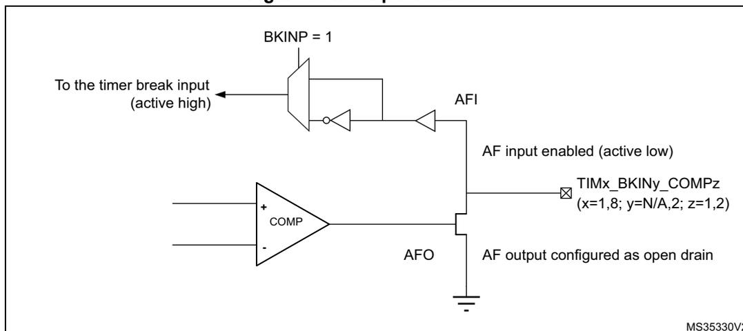
38.3.18 Clearing the OCxREF signal on an external event
The OCxREF signal of a given channel can be cleared when a high level is applied on the ocref_clr_int input (OCxCE enable bit in the corresponding TIMx_CCMRx register set to 1). OCxREF remains low until the next transition to the active state, on the following PWM
cycle. This function can only be used in Output compare and PWM modes. It does not work in Forced mode. The ocref_clr_int is connected to the ETRF signal (ETR after filtering).
When ETRF is chosen, ETR must be configured as follows:
- 1. The External Trigger Prescaler should be kept off: bits ETPS[1:0] of the TIMx_SMCR register set to '00'.
- 2. The external clock mode 2 must be disabled: bit ECE of the TIMx_SMCR register set to '0'.
- 3. The External Trigger Polarity (ETP) and the External Trigger Filter (ETF) can be configured according to the user needs.
Figure 392 shows the behavior of the OCxREF signal when the ETRF Input becomes High, for both values of the enable bit OCxCE. In this example, the timer TIMx is programmed in PWM mode.
Figure 392. Clearing TIMx OCxREF
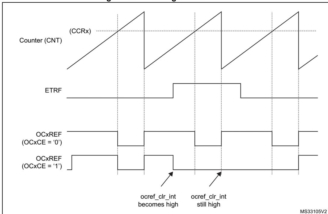
The figure is a timing diagram with four horizontal axes. The top axis is labeled 'Counter (CNT) (CCRx)' and shows a sawtooth waveform. The second axis is labeled 'ETRF' and shows a rectangular pulse. The third axis is labeled 'OCxREF (OCxCE = '0')' and shows a rectangular pulse. The bottom axis is labeled 'OCxREF (OCxCE = '1')' and shows a rectangular pulse. Vertical dashed lines indicate time intervals. Two arrows point to the bottom signal: the first arrow points to a rising edge labeled 'ocref_clr_int becomes high', and the second arrow points to a high level labeled 'ocref_clr_int still high'. The signal 'OCxREF (OCxCE = '1')' is high when ETRF is high and low when ETRF is low. The signal 'OCxREF (OCxCE = '0')' is high when ETRF is high and low when ETRF is low. The signal 'Counter (CNT) (CCRx)' is a sawtooth waveform that increases linearly and then resets to zero. The signal 'ETRF' is a rectangular pulse that is high for a certain duration. The signal 'OCxREF (OCxCE = '0')' is a rectangular pulse that is high when ETRF is high and low when ETRF is low. The signal 'OCxREF (OCxCE = '1')' is a rectangular pulse that is high when ETRF is high and low when ETRF is low. The signal 'ocref_clr_int' is a signal that becomes high when ETRF is high and remains high until the next counter overflow.
Note: In case of a PWM with a 100% duty cycle (if \( CCRx > ARR \) ), then OCxREF is enabled again at the next counter overflow.
38.3.19 6-step PWM generation
When complementary outputs are used on a channel, preload bits are available on the OCxM, CCxE and CCxNE bits. The preload bits are transferred to the shadow bits at the COM commutation event. Thus one can program in advance the configuration for the next step and change the configuration of all the channels at the same time. COM can be generated by software by setting the COM bit in the TIMx_EGR register or by hardware (on TRGI rising edge).
A flag is set when the COM event occurs (COMIF bit in the TIMx_SR register), which can generate an interrupt (if the COMIE bit is set in the TIMx_DIER register) or a DMA request (if the COMDE bit is set in the TIMx_DIER register).
The Figure 393 describes the behavior of the OCx and OCxN outputs when a COM event occurs, in 3 different examples of programmed configurations.
Figure 393. 6-step generation, COM example (OSSR=1)
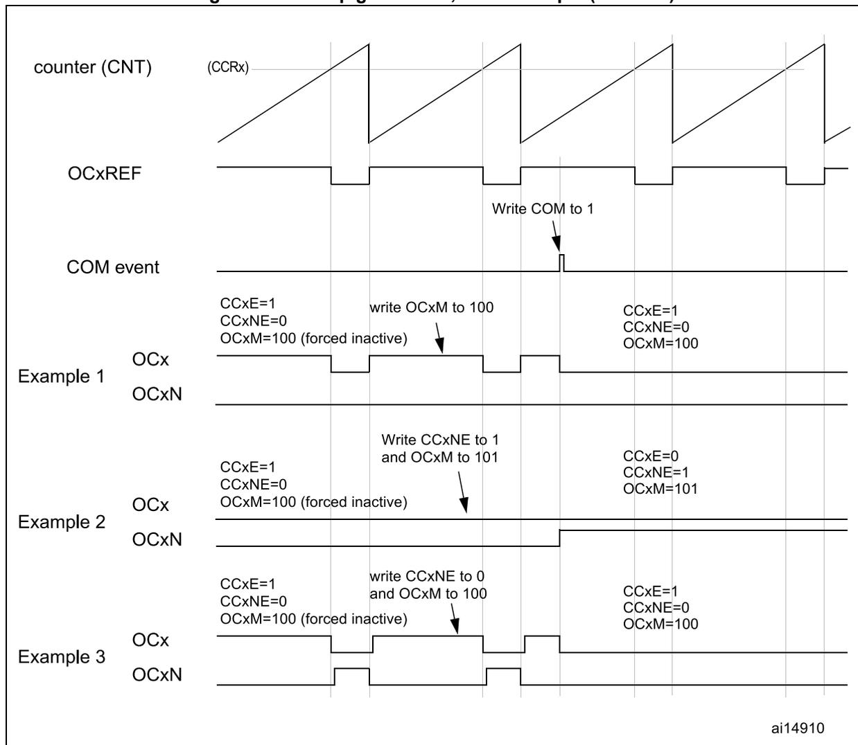
The diagram illustrates the timing of a 6-step PWM generation using complementary outputs. The top trace shows the counter (CNT) with a sawtooth waveform and a compare register (CCRx). Below it is the OCxREF signal, which is a square wave. A 'COM event' is indicated by a pulse. The diagram then shows three examples of OCx and OCxN output behaviors, each with a different configuration change triggered by the COM event.
Example 1: Initial configuration: CCxE=1, CCxNE=0, OCxM=100 (forced inactive). A write to OCxM=100 occurs. After the COM event, the configuration remains CCxE=1, CCxNE=0, OCxM=100. The OCx output is initially high and becomes low after the COM event. The OCxN output is initially low and becomes high after the COM event.
Example 2: Initial configuration: CCxE=1, CCxNE=0, OCxM=100 (forced inactive). A write to CCxNE=1 and OCxM=101 occurs. After the COM event, the configuration becomes CCxE=0, CCxNE=1, OCxM=101. The OCx output is initially high and becomes low after the COM event. The OCxN output is initially low and becomes high after the COM event.
Example 3: Initial configuration: CCxE=1, CCxNE=0, OCxM=100 (forced inactive). A write to CCxNE=0 and OCxM=100 occurs. After the COM event, the configuration remains CCxE=1, CCxNE=0, OCxM=100. The OCx output is initially high and becomes low after the COM event. The OCxN output is initially low and becomes high after the COM event.
ai14910
38.3.20 One-pulse mode
One-pulse mode (OPM) is a particular case of the previous modes. It allows the counter to be started in response to a stimulus and to generate a pulse with a programmable length after a programmable delay.
Starting the counter can be controlled through the slave mode controller. Generating the waveform can be done in output compare mode or PWM mode. One-pulse mode is selected by setting the OPM bit in the TIMx_CR1 register. This makes the counter stop automatically at the next update event UEV.
A pulse can be correctly generated only if the compare value is different from the counter initial value. Before starting (when the timer is waiting for the trigger), the configuration must be:
- • In upcounting: \( CNT < CCRx \leq ARR \) (in particular, \( 0 < CCRx \) )
- • In downcounting: \( CNT > CCRx \)
Figure 394. Example of one pulse mode.
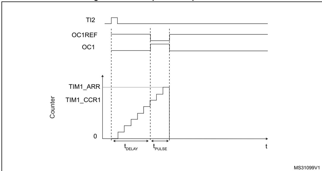
For example one may want to generate a positive pulse on OC1 with a length of \( t_{PULSE} \) and after a delay of \( t_{DELAY} \) as soon as a positive edge is detected on the TI2 input pin.
Let's use TI2FP2 as trigger 1:
- 1. Select the proper TI2x source (internal or external) with the TI2SEL[3:0] bits in the TIMx_TISEL register.
- 2. Map TI2FP2 to TI2 by writing CC2S='01' in the TIMx_CCMR1 register.
- 3. TI2FP2 must detect a rising edge, write CC2P='0' and CC2NP='0' in the TIMx_CCER register.
- 4. Configure TI2FP2 as trigger for the slave mode controller (TRGI) by writing TS=00110 in the TIMx_SMCR register.
- 5. TI2FP2 is used to start the counter by writing SMS to '110' in the TIMx_SMCR register (trigger mode).
The OPM waveform is defined by writing the compare registers (taking into account the clock frequency and the counter prescaler).
- • The \( t_{\text{DELAY}} \) is defined by the value written in the TIMx_CCR1 register.
- • The \( t_{\text{PULSE}} \) is defined by the difference between the auto-reload value and the compare value (TIMx_ARR - TIMx_CCR1).
- • Let's say one wants to build a waveform with a transition from '0' to '1' when a compare match occurs and a transition from '1' to '0' when the counter reaches the auto-reload value. To do this PWM mode 2 must be enabled by writing OC1M=111 in the TIMx_CCMR1 register. Optionally the preload registers can be enabled by writing OC1PE='1' in the TIMx_CCMR1 register and ARPE in the TIMx_CR1 register. In this case one has to write the compare value in the TIMx_CCR1 register, the auto-reload value in the TIMx_ARR register, generate an update by setting the UG bit and wait for external trigger event on TI2. CC1P is written to '0' in this example.
In our example, the DIR and CMS bits in the TIMx_CR1 register should be low.
Since only 1 pulse (Single mode) is needed, a 1 must be written in the OPM bit in the TIMx_CR1 register to stop the counter at the next update event (when the counter rolls over from the auto-reload value back to 0). When OPM bit in the TIMx_CR1 register is set to '0', so the Repetitive Mode is selected.
Particular case: OCx fast enable:
In One-pulse mode, the edge detection on TIx input set the CEN bit which enables the counter. Then the comparison between the counter and the compare value makes the output toggle. But several clock cycles are needed for these operations and it limits the minimum delay \( t_{\text{DELAY min}} \) we can get.
If one wants to output a waveform with the minimum delay, the OCxFE bit can be set in the TIMx_CCMRx register. Then OCxRef (and OCx) are forced in response to the stimulus, without taking in account the comparison. Its new level is the same as if a compare match had occurred. OCxFE acts only if the channel is configured in PWM1 or PWM2 mode.
38.3.21 Retriggerable one pulse mode
This mode allows the counter to be started in response to a stimulus and to generate a pulse with a programmable length, but with the following differences with Non-retriggerable one pulse mode described in Section 38.3.20 :
- – The pulse starts as soon as the trigger occurs (no programmable delay)
- – The pulse is extended if a new trigger occurs before the previous one is completed
The timer must be in Slave mode, with the bits SMS[3:0] = '1000' (Combined Reset + trigger mode) in the TIMx_SMCR register, and the OCxM[3:0] bits set to '1000' or '1001' for retriggerable OPM mode 1 or 2.
If the timer is configured in Up-counting mode, the corresponding CCRx must be set to 0 (the ARR register sets the pulse length). If the timer is configured in Down-counting mode, CCRx must be above or equal to ARR.
Note: The OCxM[3:0] and SMS[3:0] bit fields are split into two parts for compatibility reasons, the most significant bit are not contiguous with the 3 least significant ones.
This mode must not be used with center-aligned PWM modes. It is mandatory to have CMS[1:0] = 00 in TIMx_CR1.
Figure 395. Retriggerable one pulse mode
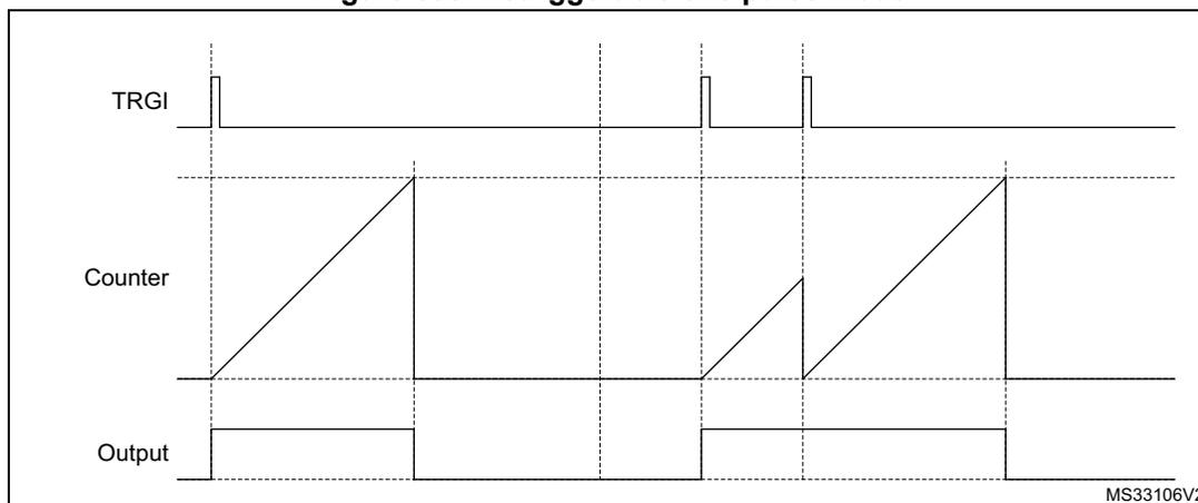
MS33106V2
38.3.22 Encoder interface mode
To select Encoder Interface mode write SMS='001' in the TIMx_SMCR register if the counter is counting on TI2 edges only, SMS='010' if it is counting on TI1 edges only and SMS='011' if it is counting on both TI1 and TI2 edges.
Select the TI1 and TI2 polarity by programming the CC1P and CC2P bits in the TIMx_CCER register. When needed, the input filter can be programmed as well. CC1NP and CC2NP must be kept low.
The two inputs TI1 and TI2 are used to interface to a quadrature encoder. Refer to Table 332 . The counter is clocked by each valid transition on TI1FP1 or TI2FP2 (TI1 and TI2 after input filter and polarity selection, TI1FP1=TI1 if not filtered and not inverted, TI2FP2=TI2 if not filtered and not inverted) assuming that it is enabled (CEN bit in TIMx_CR1 register written to '1'). The sequence of transitions of the two inputs is evaluated and generates count pulses as well as the direction signal. Depending on the sequence the counter counts up or down, the DIR bit in the TIMx_CR1 register is modified by hardware accordingly. The DIR bit is calculated at each transition on any input (TI1 or TI2), whatever the counter is counting on TI1 only, TI2 only or both TI1 and TI2.
Encoder interface mode acts simply as an external clock with direction selection. This means that the counter just counts continuously between 0 and the auto-reload value in the TIMx_ARR register (0 to ARR or ARR down to 0 depending on the direction). So the TIMx_ARR must be configured before starting. In the same way, the capture, compare, repetition counter, trigger output features continue to work as normal. Encoder mode and External clock mode 2 are not compatible and must not be selected together.
Note: The prescaler must be set to zero when encoder mode is enabled
In this mode, the counter is modified automatically following the speed and the direction of the quadrature encoder and its content, therefore, always represents the encoder's position. The count direction correspond to the rotation direction of the connected sensor. The table summarizes the possible combinations, assuming TI1 and TI2 do not switch at the same time.
Table 332. Counting direction versus encoder signals
| Active edge | Level on opposite signal (TI1FP1 for TI2, TI2FP2 for TI1) | TI1FP1 signal | TI2FP2 signal | ||
|---|---|---|---|---|---|
| Rising | Falling | Rising | Falling | ||
| Counting on TI1 only | High | Down | Up | No Count | No Count |
| Low | Up | Down | No Count | No Count | |
| Counting on TI2 only | High | No Count | No Count | Up | Down |
| Low | No Count | No Count | Down | Up | |
| Counting on TI1 and TI2 | High | Down | Up | Up | Down |
| Low | Up | Down | Down | Up | |
A quadrature encoder can be connected directly to the MCU without external interface logic. However, comparators are normally used to convert the encoder's differential outputs to digital signals. This greatly increases noise immunity. The third encoder output which indicates the mechanical zero position, may be connected to an external interrupt input and trigger a counter reset.
The Figure 396 gives an example of counter operation, showing count signal generation and direction control. It also shows how input jitter is compensated where both edges are selected. This might occur if the sensor is positioned near to one of the switching points. For this example we assume that the configuration is the following:
- • CC1S='01' (TIMx_CCMR1 register, TI1FP1 mapped on TI1).
- • CC2S='01' (TIMx_CCMR2 register, TI1FP2 mapped on TI2).
- • CC1P='0' and CC1NP='0' (TIMx_CCER register, TI1FP1 non-inverted, TI1FP1=TI1).
- • CC2P='0' and CC2NP='0' (TIMx_CCER register, TI1FP2 non-inverted, TI1FP2=TI2).
- • SMS='011' (TIMx_SMCR register, both inputs are active on both rising and falling edges).
- • CEN='1' (TIMx_CR1 register, Counter enabled).
Figure 396. Example of counter operation in encoder interface mode.
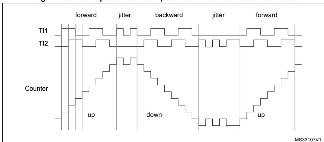
Figure 397 gives an example of counter behavior when TI1FP1 polarity is inverted (same configuration as above except CC1P='1').
Figure 397. Example of encoder interface mode with TI1FP1 polarity inverted.
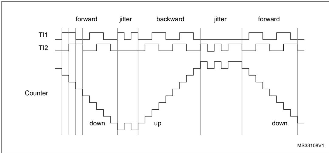
The timer, when configured in Encoder Interface mode provides information on the sensor's current position. Dynamic information can be obtained (speed, acceleration, deceleration) by measuring the period between two encoder events using a second timer configured in capture mode. The output of the encoder which indicates the mechanical zero can be used for this purpose. Depending on the time between two events, the counter can also be read at regular times. This can be done by latching the counter value into a third input capture register if available (then the capture signal must be periodic and can be generated by another timer). When available, it is also possible to read its value through a DMA request.
The IUFREMAP bit in the TIMx_CR1 register forces a continuous copy of the update interrupt flag (UIF) into the timer counter register's bit 31 (TIMxCNT[31]). This allows both the counter value and a potential roll-over condition signaled by the UIFCPY flag to be read in an atomic way. It eases the calculation of angular speed by avoiding race conditions caused, for instance, by a processing shared between a background task (counter reading) and an interrupt (update interrupt).
There is no latency between the UIF and UIFCPY flag assertions.
In 32-bit timer implementations, when the IUFREMAP bit is set, bit 31 of the counter is overwritten by the UIFCPY flag upon read access (the counter's most significant bit is only accessible in write mode).
38.3.23 UIF bit remapping
The IUFREMAP bit in the TIMx_CR1 register forces a continuous copy of the Update Interrupt Flag UIF into the timer counter register's bit 31 (TIMxCNT[31]). This allows both the counter value and a potential roll-over condition signaled by the UIFCPY flag to be read in an atomic way. In particular cases, it can ease the calculations by avoiding race conditions, caused for instance by a processing shared between a background task (counter reading) and an interrupt (Update Interrupt).
There is no latency between the UIF and UIFCPY flags assertion.
38.3.24 Timer input XOR function
The TI1S bit in the TIMx_CR2 register, allows the input filter of channel 1 to be connected to the output of an XOR gate, combining the three input pins TIMx_CH1, TIMx_CH2 and TIMx_CH3.
The XOR output can be used with all the timer input functions such as trigger or input capture. It is convenient to measure the interval between edges on two input signals, as per Figure 398 below.
Figure 398. Measuring time interval between edges on 3 signals
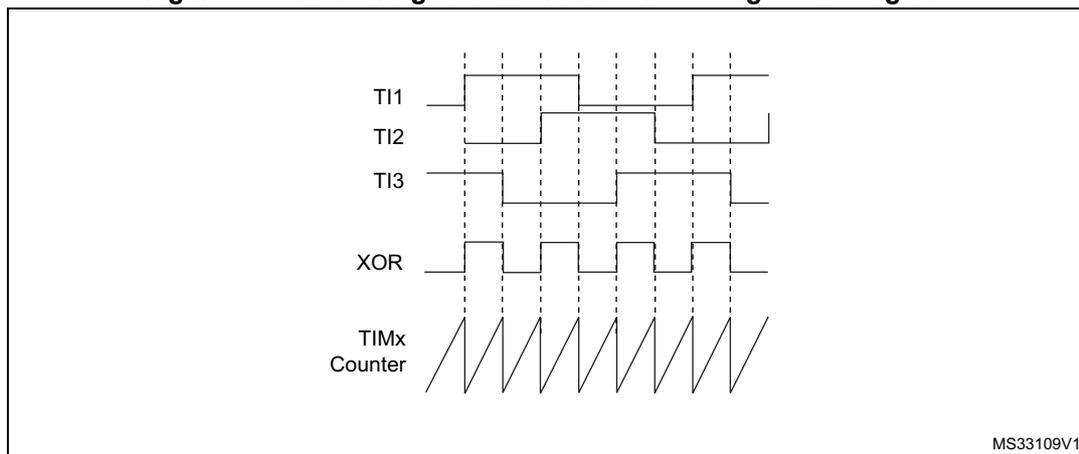
The figure is a timing diagram with five horizontal axes. From top to bottom, they are labeled: TI1, TI2, TI3, XOR, and TIMx Counter. - TI1, TI2, and TI3 are digital signals with various pulse widths and spacings. - The XOR signal is the logical XOR of TI1, TI2, and TI3. It has a pulse whenever an odd number of the three inputs are high. - The TIMx Counter is a sawtooth waveform that increases linearly and then drops abruptly to zero. The drops occur precisely at the rising and falling edges of the XOR signal. - Vertical dashed lines connect the edges of the XOR signal to the corresponding reset points of the counter. - In the bottom right corner of the diagram area, there is a small text label: MS33109V1.
38.3.25 Interfacing with Hall sensors
This is done using the advanced-control timers (TIM1 or TIM8) to generate PWM signals to drive the motor and another timer TIMx (TIM2, TIM3, TIM4) referred to as “interfacing timer” in Figure 399. The “interfacing timer” captures the 3 timer input pins (CC1, CC2, CC3) connected through a XOR to the TI1 input channel (selected by setting the TI1S bit in the TIMx_CR2 register).
The slave mode controller is configured in reset mode; the slave input is TI1F_ED. Thus, each time one of the 3 inputs toggles, the counter restarts counting from 0. This creates a time base triggered by any change on the Hall inputs.
On the “interfacing timer”, capture/compare channel 1 is configured in capture mode, capture signal is TRC (See Figure 372: Capture/compare channel (example: channel 1 input stage) on page 1549 ). The captured value, which corresponds to the time elapsed between 2 changes on the inputs, gives information about motor speed.
The “interfacing timer” can be used in output mode to generate a pulse which changes the configuration of the channels of the advanced-control timer (TIM1 or TIM8) (by triggering a COM event). The TIM1 timer is used to generate PWM signals to drive the motor. To do this, the interfacing timer channel must be programmed so that a positive pulse is generated after a programmed delay (in output compare or PWM mode). This pulse is sent to the advanced-control timer (TIM1 or TIM8) through the TRGO output.
Example: one wants to change the PWM configuration of the advanced-control timer TIM1 after a programmed delay each time a change occurs on the Hall inputs connected to one of the TIMx timers.
- • Configure 3 timer inputs ORed to the TI1 input channel by writing the TI1S bit in the TIMx_CR2 register to '1',
- • Program the time base: write the TIMx_ARR to the max value (the counter must be cleared by the TI1 change. Set the prescaler to get a maximum counter period longer than the time between 2 changes on the sensors,
- • Program the channel 1 in capture mode (TRC selected): write the CC1S bits in the TIMx_CCMR1 register to '01'. The digital filter can also be programmed if needed,
- • Program the channel 2 in PWM 2 mode with the desired delay: write the OC2M bits to '111' and the CC2S bits to '00' in the TIMx_CCMR1 register,
- • Select OC2REF as trigger output on TRGO: write the MMS bits in the TIMx_CR2 register to '101',
In the advanced-control timer TIM1, the right ITR input must be selected as trigger input, the timer is programmed to generate PWM signals, the capture/compare control signals are preloaded (CCPC=1 in the TIMx_CR2 register) and the COM event is controlled by the trigger input (CCUS=1 in the TIMx_CR2 register). The PWM control bits (CCxE, OCxM) are written after a COM event for the next step (this can be done in an interrupt subroutine generated by the rising edge of OC2REF).
The Figure 399 describes this example.
Figure 399. Example of Hall sensor interface
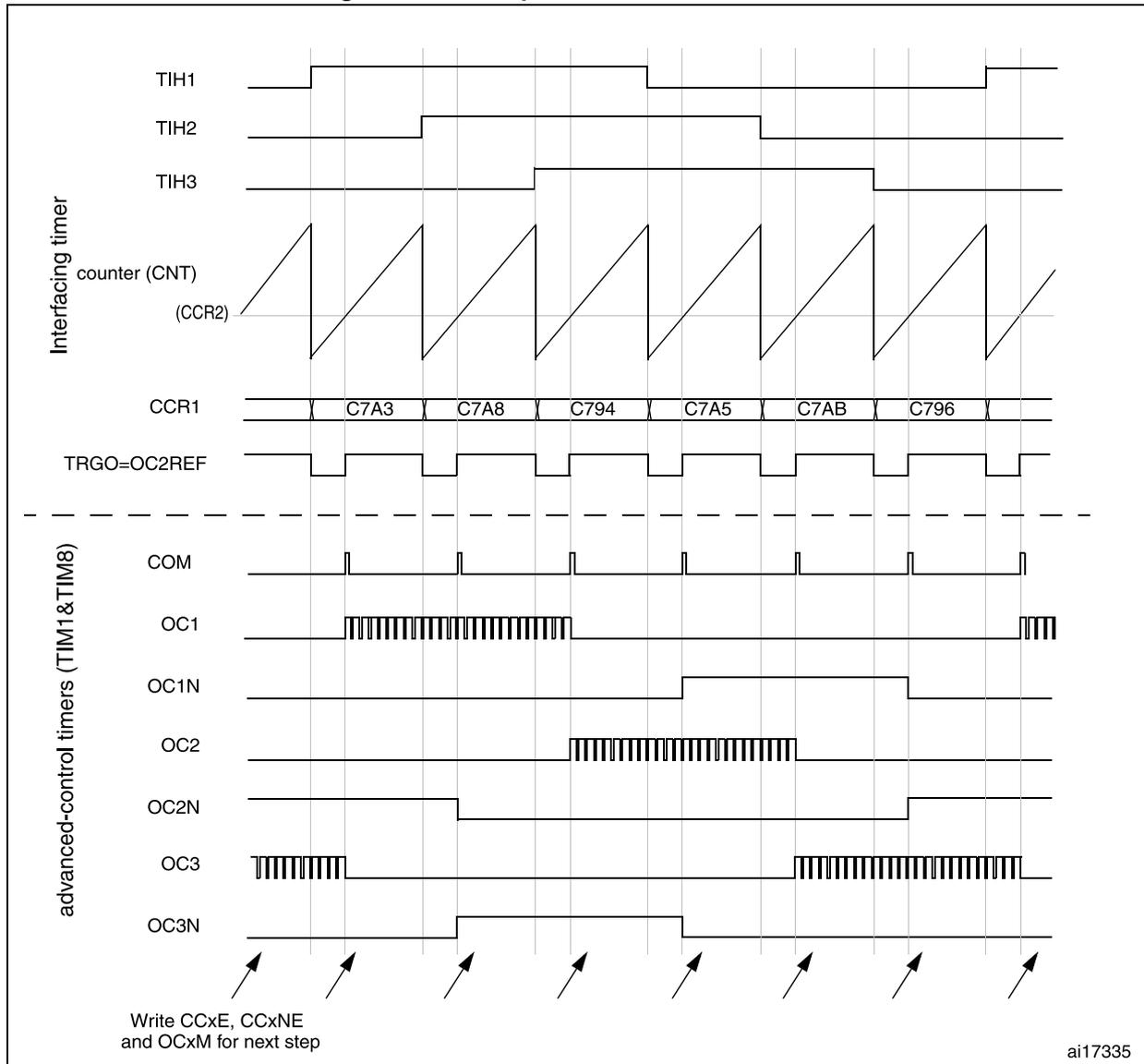
The timing diagram illustrates the operation of a Hall sensor interface. The top section, labeled 'Interfacing timer', includes signals TIH1, TIH2, and TIH3 (inputs), the counter (CNT) output (a sawtooth waveform), and CCR1 (showing values C7A3, C7A8, C794, C7A5, C7AB, C796). The TRGO=OC2REF output is also shown. A dashed line separates this from the 'advanced-control timers (TIM1&TIM8)' section, which includes COM, OC1, OC1N, OC2, OC2N, OC3, and OC3N signals. Arrows at the bottom point to specific time intervals with the text 'Write CCxE, CCxNE and OCxM for next step'. The identifier 'ai17335' is in the bottom right corner.
38.3.26 Timer synchronization
The TIMx timers are linked together internally for timer synchronization or chaining. Refer to Section 39.3.19: Timer synchronization for details. They can be synchronized in several modes: Reset mode, Gated mode, and Trigger mode.
Slave mode: Reset mode
The counter and its prescaler can be reinitialized in response to an event on a trigger input. Moreover, if the URS bit from the TIMx_CR1 register is low, an update event UEV is generated. Then all the preloaded registers (TIMx_ARR, TIMx_CCRx) are updated.
In the following example, the upcounter is cleared in response to a rising edge on TI1 input:
- • Configure the channel 1 to detect rising edges on TI1. Configure the input filter duration (in this example, we do not need any filter, so we keep IC1F=0000). The capture prescaler is not used for triggering, so it does not need to be configured. The CC1S bits select the input capture source only, CC1S = 01 in the TIMx_CCMR1 register. Write CC1P=0 and CC1NP='0' in TIMx_CCER register to validate the polarity (and detect rising edges only).
- • Configure the timer in reset mode by writing SMS=100 in TIMx_SMCR register. Select TI1 as the input source by writing TS=00101 in TIMx_SMCR register.
- • Start the counter by writing CEN=1 in the TIMx_CR1 register.
The counter starts counting on the internal clock, then behaves normally until TI1 rising edge. When TI1 rises, the counter is cleared and restarts from 0. In the meantime, the trigger flag is set (TIF bit in the TIMx_SR register) and an interrupt request, or a DMA request can be sent if enabled (depending on the TIE and TDE bits in TIMx_DIER register).
The following figure shows this behavior when the auto-reload register TIMx_ARR=0x36. The delay between the rising edge on TI1 and the actual reset of the counter is due to the resynchronization circuit on TI1 input.
Figure 400. Control circuit in reset mode
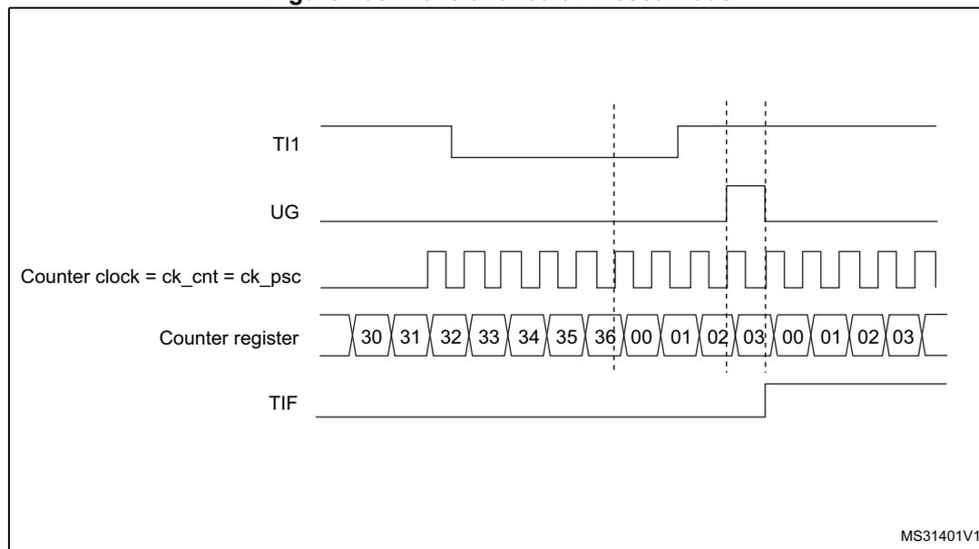
MS31401V1
Slave mode: Gated mode
The counter can be enabled depending on the level of a selected input.
In the following example, the upcounter counts only when TI1 input is low:
- • Configure the channel 1 to detect low levels on TI1. Configure the input filter duration (in this example, we do not need any filter, so we keep IC1F=0000). The capture prescaler is not used for triggering, so it does not need to be configured. The CC1S bits select the input capture source only, CC1S=01 in TIMx_CCMR1 register. Write CC1P=1 and CC1NP=0' in TIMx_CCER register to validate the polarity (and detect low level only).
- • Configure the timer in gated mode by writing SMS=101 in TIMx_SMCR register. Select TI1 as the input source by writing TS=00101 in TIMx_SMCR register.
- • Enable the counter by writing CEN=1 in the TIMx_CR1 register (in gated mode, the counter doesn't start if CEN=0, whatever is the trigger input level).
The counter starts counting on the internal clock as long as TI1 is low and stops as soon as TI1 becomes high. The TIF flag in the TIMx_SR register is set both when the counter starts or stops.
The delay between the rising edge on TI1 and the actual stop of the counter is due to the resynchronization circuit on TI1 input.
Figure 401. Control circuit in Gated mode
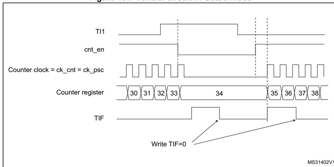
Slave mode: Trigger mode
The counter can start in response to an event on a selected input.
In the following example, the upcounter starts in response to a rising edge on TI2 input:
- • Configure the channel 2 to detect rising edges on TI2. Configure the input filter duration (in this example, we do not need any filter, so we keep IC2F=0000). The capture prescaler is not used for triggering, so it does not need to be configured. The CC2S bits are configured to select the input capture source only, CC2S=01 in TIMx_CCMR1 register.
register. Write CC2P=1 and CC2NP=0 in TIMx_CCER register to validate the polarity (and detect low level only).
- • Configure the timer in trigger mode by writing SMS=110 in TIMx_SMCR register. Select TI2 as the input source by writing TS=00110 in TIMx_SMCR register.
When a rising edge occurs on TI2, the counter starts counting on the internal clock and the TIF flag is set.
The delay between the rising edge on TI2 and the actual start of the counter is due to the resynchronization circuit on TI2 input.
Figure 402. Control circuit in trigger mode
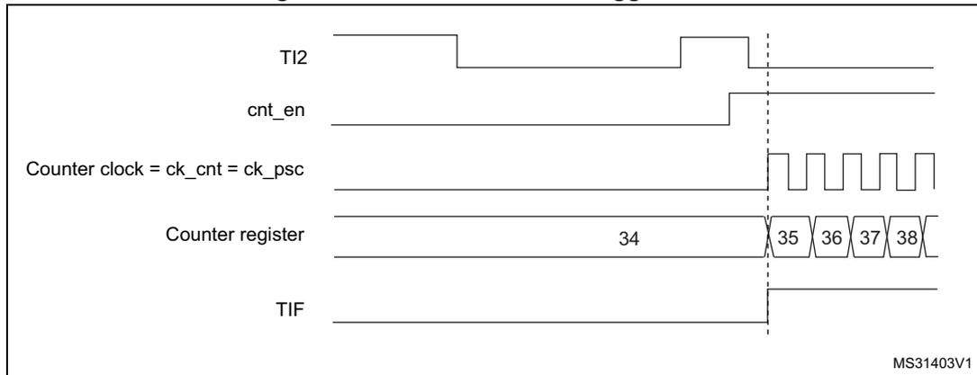
The diagram illustrates the timing of the control circuit in trigger mode. The TI2 input signal shows a rising edge. The cnt_en signal is generated by the timer logic and goes high after the rising edge of TI2. The counter clock (ck_cnt = ck_psc) is a periodic square wave. The counter register starts at 34 and increments to 35, 36, 37, and 38. The TIF flag is set high at the rising edge of TI2 and remains high.
MS31403V1
Slave mode: Combined reset + trigger mode
In this case, a rising edge of the selected trigger input (TRGI) reinitializes the counter, generates an update of the registers, and starts the counter.
This mode is used for one-pulse mode.
Slave mode: external clock mode 2 + trigger mode
The external clock mode 2 can be used in addition to another slave mode (except external clock mode 1 and encoder mode). In this case, the ETR signal is used as external clock input, and another input can be selected as trigger input (in reset mode, gated mode or trigger mode). It is recommended not to select ETR as TRGI through the TS bits of TIMx_SMCR register.
In the following example, the upcounter is incremented at each rising edge of the ETR signal as soon as a rising edge of TI1 occurs:
- 1. Configure the external trigger input circuit by programming the TIMx_SMCR register as follows:
- – ETF = 0000: no filter
- – ETPS = 00: prescaler disabled
- – ETP = 0: detection of rising edges on ETR and ECE=1 to enable the external clock mode 2.
- 2. Configure the channel 1 as follows, to detect rising edges on TI:
- – IC1F = 0000: no filter.
- – The capture prescaler is not used for triggering and does not need to be configured.
- – CC1S = 01 in TIMx_CCMR1 register to select only the input capture source
- – CC1P = 0 and CC1NP = 0 in TIMx_CCER register to validate the polarity (and detect rising edge only).
- 3. Configure the timer in trigger mode by writing SMS=110 in TIMx_SMCR register. Select TI1 as the input source by writing TS=00101 in TIMx_SMCR register.
A rising edge on TI1 enables the counter and sets the TIF flag. The counter then counts on ETR rising edges.
The delay between the rising edge of the ETR signal and the actual reset of the counter is due to the resynchronization circuit on ETRP input.
Figure 403. Control circuit in external clock mode 2 + trigger mode
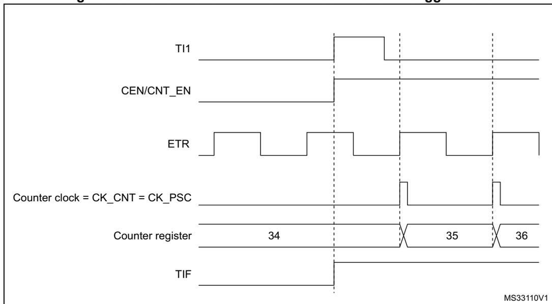
The timing diagram shows the following signals over time:
- TI1 : Input signal. A rising edge occurs at the first vertical dashed line.
- CEN/CNT_EN : Counter enable signal. It goes high at the first dashed line (triggered by TI1 rising edge) and stays high.
- ETR : External trigger signal. It is a periodic square wave. Rising edges occur at various points.
- Counter clock = CK_CNT = CK_PSC : The clock for the counter. It is initially low. It goes high at the first ETR rising edge after the counter is enabled, then low again at the next ETR rising edge, and so on. This indicates it is toggling on ETR rising edges.
- Counter register : Shows the count value. It starts at 34. It increments to 35 at the first ETR rising edge after the counter is enabled. It increments to 36 at the next ETR rising edge.
- TIF : Timer interrupt flag. It goes high at the first dashed line (TI1 rising edge) and stays high.
Note: The clock of the slave peripherals (timer, ADC, ...) receiving the TRGO or the TRGO2 signals must be enabled prior to receive events from the master timer, and the clock frequency (prescaler) must not be changed on-the-fly while triggers are received from the master timer.
38.3.27 ADC synchronization
The timer can generate an ADC triggering event with various internal signals, such as reset, enable or compare events. It is also possible to generate a pulse issued by internal edge detectors, such as:
- – Rising and falling edges of OC4ref
- – Rising edge on OC5ref or falling edge on OC6ref
The triggers are issued on the TRGO2 internal line which is redirected to the ADC. There is a total of 16 possible events, which can be selected using the MMS2[3:0] bits in the TIMx_CR2 register.
An example of an application for 3-phase motor drives is given in Figure 383 on page 1561 .
Note: The clock of the slave peripherals (timer, ADC, ...) receiving the TRGO or the TRGO2 signals must be enabled prior to receive events from the master timer, and the clock frequency (prescaler) must not be changed on-the-fly while triggers are received from the master timer.
Note: The clock of the ADC must be enabled prior to receive events from the master timer, and must not be changed on-the-fly while triggers are received from the timer.
38.3.28 DMA burst mode
The TIMx timers have the capability to generate multiple DMA requests upon a single event. The main purpose is to be able to re-program part of the timer multiple times without software overhead, but it can also be used to read several registers in a row, at regular intervals.
The DMA controller destination is unique and must point to the virtual register TIMx_DMAR. On a given timer event, the timer launches a sequence of DMA requests (burst). Each write into the TIMx_DMAR register is actually redirected to one of the timer registers.
The DBL[4:0] bits in the TIMx_DCR register set the DMA burst length. The timer recognizes a burst transfer when a read or a write access is done to the TIMx_DMAR address), i.e. the number of transfers (either in half-words or in bytes).
The DBA[4:0] bits in the TIMx_DCR registers define the DMA base address for DMA transfers (when read/write access are done through the TIMx_DMAR address). DBA is defined as an offset starting from the address of the TIMx_CR1 register:
Example:
00000: TIMx_CR1
00001: TIMx_CR2
00010: TIMx_SMCR
As an example, the timer DMA burst feature is used to update the contents of the CCRx registers (x = 2, 3, 4) upon an update event, with the DMA transferring half words into the CCRx registers.
This is done in the following steps:
- 1. Configure the corresponding DMA channel as follows:
- – DMA channel peripheral address is the DMAR register address
- – DMA channel memory address is the address of the buffer in the RAM containing the data to be transferred by DMA into CCRx registers.
- – Number of data to transfer = 3 (See note below).
- – Circular mode disabled.
- 2. Configure the DCR register by configuring the DBA and DBL bit fields as follows: DBL = 3 transfers, DBA = 0xE.
- 3. Enable the TIMx update DMA request (set the UDE bit in the DIER register).
- 4. Enable TIMx
- 5. Enable the DMA channel
This example is for the case where every CCRx register to be updated once. If every CCRx register is to be updated twice for example, the number of data to transfer should be 6. Let's take the example of a buffer in the RAM containing data1, data2, data3, data4, data5 and data6. The data is transferred to the CCRx registers as follows: on the first update DMA request, data1 is transferred to CCR2, data2 is transferred to CCR3, data3 is transferred to CCR4 and on the second update DMA request, data4 is transferred to CCR2, data5 is transferred to CCR3 and data6 is transferred to CCR4.
Note: A null value can be written to the reserved registers.
38.3.29 Debug mode
When the microcontroller enters debug mode (Cortex ® -M7 with FPU core halted), the TIMx counter either continues to work normally or stops, depending on DBG_TIMx_STOP configuration bit in DBG module.
For safety purposes, when the counter is stopped, the outputs are disabled (as if the MOE bit was reset). The outputs can either be forced to an inactive state (OSSI bit = 1), or have their control taken over by the GPIO controller (OSSI bit = 0), typically to force a Hi-Z.
For more details, refer to section Debug support (DBG).
38.4 TIM1/TIM8 registers
Refer to for a list of abbreviations used in register descriptions.
The peripheral registers can be accessed by half-words (16-bit) or words (32-bit).
38.4.1 TIMx control register 1 (TIMx_CR1)(x = 1, 8)
Address offset: 0x00
Reset value: 0x0000
| 15 | 14 | 13 | 12 | 11 | 10 | 9 | 8 | 7 | 6 | 5 | 4 | 3 | 2 | 1 | 0 |
|---|---|---|---|---|---|---|---|---|---|---|---|---|---|---|---|
| Res. | Res. | Res. | Res. | UIFREMAP | Res. | CKD[1:0] | ARPE | CMS[1:0] | DIR | OPM | URS | UDIS | CEN | ||
| rw | rw | rw | rw | rw | rw | rw | rw | rw | |||||||
Bits 15:12 Reserved, must be kept at reset value.
Bit 11 UIFREMAP : UIF status bit remapping
0: No remapping. UIF status bit is not copied to TIMx_CNT register bit 31.
1: Remapping enabled. UIF status bit is copied to TIMx_CNT register bit 31.
Bit 10 Reserved, must be kept at reset value.
Bits 9:8 CKD[1:0] : Clock division
This bit-field indicates the division ratio between the timer clock (CK_INT) frequency and the dead-time and sampling clock ( \( t_{DTS} \) ) used by the dead-time generators and the digital filters (ETR, TIx):
00: \( t_{DTS} = t_{CK\_INT} \)
01: \( t_{DTS} = 2 * t_{CK\_INT} \)
10: \( t_{DTS} = 4 * t_{CK\_INT} \)
11: Reserved, do not program this value
Note: \( t_{DTS} = 1/f_{DTS} \) , \( t_{CK\_INT} = 1/f_{CK\_INT} \) .
Bit 7 ARPE : Auto-reload preload enable
0: TIMx_ARR register is not buffered
1: TIMx_ARR register is buffered
Bits 6:5 CMS[1:0] : Center-aligned mode selection
00: Edge-aligned mode. The counter counts up or down depending on the direction bit (DIR).
01: Center-aligned mode 1. The counter counts up and down alternatively. Output compare interrupt flags of channels configured in output (CCxS=00 in TIMx_CCMRx register) are set only when the counter is counting down.
10: Center-aligned mode 2. The counter counts up and down alternatively. Output compare interrupt flags of channels configured in output (CCxS=00 in TIMx_CCMRx register) are set only when the counter is counting up.
11: Center-aligned mode 3. The counter counts up and down alternatively. Output compare interrupt flags of channels configured in output (CCxS=00 in TIMx_CCMRx register) are set both when the counter is counting up or down.
Note: Switch from edge-aligned mode to center-aligned mode as long as the counter is enabled (CEN=1) is not allowed
Bit 4 DIR : Direction- 0: Counter used as upcounter
- 1: Counter used as downcounter
Note: This bit is read only when the timer is configured in Center-aligned mode or Encoder mode.
Bit 3 OPM : One pulse mode- 0: Counter is not stopped at update event
- 1: Counter stops counting at the next update event (clearing the bit CEN)
This bit is set and cleared by software to select the UEV event sources.
- 0: Any of the following events generate an update interrupt or DMA request if enabled. These events can be:
- – Counter overflow/underflow
- – Setting the UG bit
- – Update generation through the slave mode controller
- 1: Only counter overflow/underflow generates an update interrupt or DMA request if enabled.
This bit is set and cleared by software to enable/disable UEV event generation.
- 0: UEV enabled. The Update (UEV) event is generated by one of the following events:
- – Counter overflow/underflow
- – Setting the UG bit
- – Update generation through the slave mode controller
Buffered registers are then loaded with their preload values.
- 1: UEV disabled. The Update event is not generated, shadow registers keep their value (ARR, PSC, CCRx). However the counter and the prescaler are reinitialized if the UG bit is set or if a hardware reset is received from the slave mode controller.
- 0: Counter disabled
- 1: Counter enabled
Note: External clock, gated mode and encoder mode can work only if the CEN bit has been previously set by software. However trigger mode can set the CEN bit automatically by hardware.
38.4.2 TIMx control register 2 (TIMx_CR2)(x = 1, 8)
Address offset: 0x04
Reset value: 0x0000 0000
| 31 | 30 | 29 | 28 | 27 | 26 | 25 | 24 | 23 | 22 | 21 | 20 | 19 | 18 | 17 | 16 |
|---|---|---|---|---|---|---|---|---|---|---|---|---|---|---|---|
| Res. | Res. | Res. | Res. | Res. | Res. | Res. | Res. | MMS2[3:0] | Res. | OIS6 | Res. | OIS5 | |||
| rw | rw | rw | rw | rw | rw | ||||||||||
| 15 | 14 | 13 | 12 | 11 | 10 | 9 | 8 | 7 | 6 | 5 | 4 | 3 | 2 | 1 | 0 |
| Res. | OIS4 | OIS3N | OIS3 | OIS2N | OIS2 | OIS1N | OIS1 | TI1S | MMS[2:0] | CCDS | CCUS | Res. | CCPC | ||
| rw | rw | rw | rw | rw | rw | rw | rw | rw | rw | rw | rw | rw | rw | ||
Bits 31:24 Reserved, must be kept at reset value.
Bits 23:20 MMS2[3:0] : Master mode selection 2
These bits allow the information to be sent to ADC for synchronization (TRGO2) to be selected. The combination is as follows:
0000: Reset - the UG bit from the TIMx_EGR register is used as trigger output (TRGO2). If the reset is generated by the trigger input (slave mode controller configured in reset mode), the signal on TRGO2 is delayed compared to the actual reset.
0001: Enable - the Counter Enable signal CNT_EN is used as trigger output (TRGO2). It is useful to start several timers at the same time or to control a window in which a slave timer is enabled. The Counter Enable signal is generated by a logic AND between the CEN control bit and the trigger input when configured in Gated mode. When the Counter Enable signal is controlled by the trigger input, there is a delay on TRGO2, except if the Master/Slave mode is selected (see the MSM bit description in TIMx_SMCR register).
0010: Update - the update event is selected as trigger output (TRGO2). For instance, a master timer can then be used as a prescaler for a slave timer.
0011: Compare pulse - the trigger output sends a positive pulse when the CC1IF flag is to be set (even if it was already high), as soon as a capture or compare match occurs (TRGO2).
0100: Compare - OC1REFC signal is used as trigger output (TRGO2)
0101: Compare - OC2REFC signal is used as trigger output (TRGO2)
0110: Compare - OC3REFC signal is used as trigger output (TRGO2)
0111: Compare - OC4REFC signal is used as trigger output (TRGO2)
1000: Compare - OC5REFC signal is used as trigger output (TRGO2)
1001: Compare - OC6REFC signal is used as trigger output (TRGO2)
1010: Compare Pulse - OC4REFC rising or falling edges generate pulses on TRGO2
1011: Compare Pulse - OC6REFC rising or falling edges generate pulses on TRGO2
1100: Compare Pulse - OC4REFC or OC6REFC rising edges generate pulses on TRGO2
1101: Compare Pulse - OC4REFC rising or OC6REFC falling edges generate pulses on TRGO2
1110: Compare Pulse - OC5REFC or OC6REFC rising edges generate pulses on TRGO2
1111: Compare Pulse - OC5REFC rising or OC6REFC falling edges generate pulses on TRGO2
Note: The clock of the slave timer or ADC must be enabled prior to receive events from the master timer, and must not be changed on-the-fly while triggers are received from the master timer.
Bit 19 Reserved, must be kept at reset value.
Bit 18 OIS6 : Output Idle state 6 (OC6 output)
Refer to OIS1 bit
Bit 17 Reserved, must be kept at reset value.
Bit 16 OIS5 : Output Idle state 5 (OC5 output)
Refer to OIS1 bit
Bit 15 Reserved, must be kept at reset value.
Bit 14 OIS4 : Output Idle state 4 (OC4 output)
Refer to OIS1 bit
Bit 13 OIS3N : Output Idle state 3 (OC3N output)
Refer to OIS1N bit
Bit 12 OIS3 : Output Idle state 3 (OC3 output)
Refer to OIS1 bit
Bit 11 OIS2N : Output Idle state 2 (OC2N output)
Refer to OIS1N bit
Bit 10 OIS2 : Output Idle state 2 (OC2 output)
Refer to OIS1 bit
Bit 9 OIS1N : Output Idle state 1 (OC1N output)
0: OC1N=0 after a dead-time when MOE=0
1: OC1N=1 after a dead-time when MOE=0
Note: This bit can not be modified as long as LOCK level 1, 2 or 3 has been programmed (LOCK bits in TIMx_BDTR register).
Bit 8 OIS1 : Output Idle state 1 (OC1 output)
0: OC1=0 (after a dead-time if OC1N is implemented) when MOE=0
1: OC1=1 (after a dead-time if OC1N is implemented) when MOE=0
Note: This bit can not be modified as long as LOCK level 1, 2 or 3 has been programmed (LOCK bits in TIMx_BDTR register).
Bit 7 TI1S : TI1 selection
0: The TIMx_CH1 pin is connected to TI1 input
1: The TIMx_CH1, CH2 and CH3 pins are connected to the TI1 input (XOR combination)
Bits 6:4 MMS[2:0] : Master mode selection
These bits allow selected information to be sent in master mode to slave timers for synchronization (TRGO). The combination is as follows:
000: Reset - the UG bit from the TIMx_EGR register is used as trigger output (TRGO). If the reset is generated by the trigger input (slave mode controller configured in reset mode) then the signal on TRGO is delayed compared to the actual reset.
001: Enable - the Counter Enable signal CNT_EN is used as trigger output (TRGO). It is useful to start several timers at the same time or to control a window in which a slave timer is enable. The Counter Enable signal is generated by a logic AND between CEN control bit and the trigger input when configured in gated mode. When the Counter Enable signal is controlled by the trigger input, there is a delay on TRGO, except if the master/slave mode is selected (see the MSM bit description in TIMx_SMCR register).
010: Update - The update event is selected as trigger output (TRGO). For instance a master timer can then be used as a prescaler for a slave timer.
011: Compare Pulse - The trigger output send a positive pulse when the CC1IF flag is to be set (even if it was already high), as soon as a capture or a compare match occurred. (TRGO).
100: Compare - OC1REFC signal is used as trigger output (TRGO)
101: Compare - OC2REFC signal is used as trigger output (TRGO)
110: Compare - OC3REFC signal is used as trigger output (TRGO)
111: Compare - OC4REFC signal is used as trigger output (TRGO)
Note: The clock of the slave timer or ADC must be enabled prior to receive events from the master timer, and must not be changed on-the-fly while triggers are received from the master timer.
Bit 3 CCDS : Capture/compare DMA selection
0: CCx DMA request sent when CCx event occurs
1: CCx DMA requests sent when update event occurs
Bit 2 CCUS : Capture/compare control update selection
0: When capture/compare control bits are preloaded (CCPC=1), they are updated by setting the COMG bit only
1: When capture/compare control bits are preloaded (CCPC=1), they are updated by setting the COMG bit or when an rising edge occurs on TRGI
Note: This bit acts only on channels that have a complementary output.
Bit 1 Reserved, must be kept at reset value.
Bit 0 CCPC : Capture/compare preloaded control
0: CCxE, CCxNE and OCxM bits are not preloaded
1: CCxE, CCxNE and OCxM bits are preloaded, after having been written, they are updated only when a commutation event (COM) occurs (COMG bit set or rising edge detected on TRGI, depending on the CCUS bit).
Note: This bit acts only on channels that have a complementary output.
38.4.3 TIMx slave mode control register (TIMx_SMCR)(x = 1, 8)
Address offset: 0x08
Reset value: 0x0000 0000
| 31 | 30 | 29 | 28 | 27 | 26 | 25 | 24 | 23 | 22 | 21 | 20 | 19 | 18 | 17 | 16 | |||||
|---|---|---|---|---|---|---|---|---|---|---|---|---|---|---|---|---|---|---|---|---|
| Res. | Res. | Res. | Res. | Res. | Res. | Res. | Res. | Res. | Res. | TS[4:3] | Res. | Res. | Res. | Res. | SMS[3] | |||||
| rw | rw | rw | ||||||||||||||||||
| 15 | 14 | 13 | 12 | 11 | 10 | 9 | 8 | 7 | 6 | 5 | 4 | 3 | 2 | 1 | 0 | |||||
| ETP | ECE | ETPS[1:0] | ETRF[3:0] | MSM | TS[2:0] | Res. | SMS[2:0] | |||||||||||||
| rw | rw | rw | rw | rw | rw | rw | rw | rw | rw | |||||||||||
Bits 31:22 Reserved, must be kept at reset value.
Bits 19:17 Reserved, must be kept at reset value.
Bit 15 ETP : External trigger polarity
This bit selects whether ETR or \( \overline{ETR} \) is used for trigger operations
0: ETR is non-inverted, active at high level or rising edge.
1: ETR is inverted, active at low level or falling edge.
Bit 14 ECE : External clock enable
This bit enables External clock mode 2.
0: External clock mode 2 disabled
1: External clock mode 2 enabled. The counter is clocked by any active edge on the ETRF signal.
Note: Setting the ECE bit has the same effect as selecting external clock mode 1 with TRGI connected to ETRF (SMS=111 and TS=00111).
It is possible to simultaneously use external clock mode 2 with the following slave modes: reset mode, gated mode and trigger mode. Nevertheless, TRGI must not be connected to ETRF in this case (TS bits must not be 00111).
If external clock mode 1 and external clock mode 2 are enabled at the same time, the external clock input is ETRF.
Bits 13:12 ETPS[1:0] : External trigger prescalerExternal trigger signal ETRP frequency must be at most 1/4 of \( f_{CK\_INT} \) frequency. A prescaler can be enabled to reduce ETRP frequency. It is useful when inputting fast external clocks.
00: Prescaler OFF
01: ETRP frequency divided by 2
10: ETRP frequency divided by 4
11: ETRP frequency divided by 8
Bits 11:8 ETF[3:0] : External trigger filterThis bit-field then defines the frequency used to sample ETRP signal and the length of the digital filter applied to ETRP. The digital filter is made of an event counter in which N consecutive events are needed to validate a transition on the output:
0000: No filter, sampling is done at \( f_{DTS} \)
0001: \( f_{SAMPLING}=f_{CK\_INT} \) , N=2
0010: \( f_{SAMPLING}=f_{CK\_INT} \) , N=4
0011: \( f_{SAMPLING}=f_{CK\_INT} \) , N=8
0100: \( f_{SAMPLING}=f_{DTS}/2 \) , N=6
0101: \( f_{SAMPLING}=f_{DTS}/2 \) , N=8
0110: \( f_{SAMPLING}=f_{DTS}/4 \) , N=6
0111: \( f_{SAMPLING}=f_{DTS}/4 \) , N=8
1000: \( f_{SAMPLING}=f_{DTS}/8 \) , N=6
1001: \( f_{SAMPLING}=f_{DTS}/8 \) , N=8
1010: \( f_{SAMPLING}=f_{DTS}/16 \) , N=5
1011: \( f_{SAMPLING}=f_{DTS}/16 \) , N=6
1100: \( f_{SAMPLING}=f_{DTS}/16 \) , N=8
1101: \( f_{SAMPLING}=f_{DTS}/32 \) , N=5
1110: \( f_{SAMPLING}=f_{DTS}/32 \) , N=6
1111: \( f_{SAMPLING}=f_{DTS}/32 \) , N=8
Bit 7 MSM : Master/slave mode0: No action
1: The effect of an event on the trigger input (TRGI) is delayed to allow a perfect synchronization between the current timer and its slaves (through TRGO). It is useful if we want to synchronize several timers on a single external event.
Bits 21, 20, 6, 5, 4 TS[4:0] : Trigger selectionThis bit-field selects the trigger input to be used to synchronize the counter.
00000: Internal Trigger 0 (ITR0)
00001: Internal Trigger 1 (ITR1)
00010: Internal Trigger 2 (ITR2)
00011: Internal Trigger 3 (ITR3)
00100: TI1 Edge Detector (TI1F_ED)
00101: Filtered Timer Input 1 (TI1FP1)
00110: Filtered Timer Input 2 (TI2FP2)
00111: External Trigger input (ETRF)
Others: Reserved
See Table 333: TIMx internal trigger connection on page 1592 for more details on ITRx meaning for each Timer.
Note: These bits must be changed only when they are not used (e.g. when SMS=000) to avoid wrong edge detections at the transition.
Bit 3 Reserved, must be kept at reset value.
Bits 16, 2, 1, 0 SMS[3:0] : Slave mode selection
When external signals are selected the active edge of the trigger signal (TRGI) is linked to the polarity selected on the external input (see Input Control register and Control Register description).
- 0000: Slave mode disabled - if CEN = '1' then the prescaler is clocked directly by the internal clock.
- 0001: Encoder mode 1 - Counter counts up/down on TI1FP1 edge depending on TI2FP2 level.
- 0010: Encoder mode 2 - Counter counts up/down on TI2FP2 edge depending on TI1FP1 level.
- 0011: Encoder mode 3 - Counter counts up/down on both TI1FP1 and TI2FP2 edges depending on the level of the other input.
- 0100: Reset Mode - Rising edge of the selected trigger input (TRGI) reinitializes the counter and generates an update of the registers.
- 0101: Gated Mode - The counter clock is enabled when the trigger input (TRGI) is high. The counter stops (but is not reset) as soon as the trigger becomes low. Both start and stop of the counter are controlled.
- 0110: Trigger Mode - The counter starts at a rising edge of the trigger TRGI (but it is not reset). Only the start of the counter is controlled.
- 0111: External Clock Mode 1 - Rising edges of the selected trigger (TRGI) clock the counter.
- 1000: Combined reset + trigger mode - Rising edge of the selected trigger input (TRGI) reinitializes the counter, generates an update of the registers and starts the counter.
- Codes above 1000: Reserved.
Note: The gated mode must not be used if TI1F_ED is selected as the trigger input (TS=00100). Indeed, TI1F_ED outputs 1 pulse for each transition on TI1F, whereas the gated mode checks the level of the trigger signal.
Note: The clock of the slave peripherals (timer, ADC, ...) receiving the TRGO or the TRGO2 signals must be enabled prior to receive events from the master timer, and the clock frequency (prescaler) must not be changed on-the-fly while triggers are received from the master timer.
Table 333. TIMx internal trigger connection
| Slave TIM | ITR0 (TS = 00000) | ITR1 (TS = 00001) | ITR2 (TS = 00010) | ITR3 (TS = 00011) |
|---|---|---|---|---|
| TIM1 | TIM15 | TIM2 | TIM3 | TIM4 |
| TIM8 | TIM1 | TIM2 | TIM4 | TIM5 |
38.4.4 TIMx DMA/interrupt enable register (TIMx_DIER)(x = 1, 8)
Address offset: 0x0C
Reset value: 0x0000
| 15 | 14 | 13 | 12 | 11 | 10 | 9 | 8 | 7 | 6 | 5 | 4 | 3 | 2 | 1 | 0 |
|---|---|---|---|---|---|---|---|---|---|---|---|---|---|---|---|
| Res. | TDE | COMDE | CC4DE | CC3DE | CC2DE | CC1DE | UDE | BIE | TIE | COMIE | CC4IE | CC3IE | CC2IE | CC1IE | UIE |
| rw | rw | rw | rw | rw | rw | rw | rw | rw | rw | rw | rw | rw | rw | rw |
- Bit 15 Reserved, must be kept at reset value.
- Bit 14
TDE
: Trigger DMA request enable
0: Trigger DMA request disabled
1: Trigger DMA request enabled - Bit 13
COMDE
: COM DMA request enable
0: COM DMA request disabled
1: COM DMA request enabled - Bit 12
CC4DE
: Capture/Compare 4 DMA request enable
0: CC4 DMA request disabled
1: CC4 DMA request enabled - Bit 11
CC3DE
: Capture/Compare 3 DMA request enable
0: CC3 DMA request disabled
1: CC3 DMA request enabled - Bit 10
CC2DE
: Capture/Compare 2 DMA request enable
0: CC2 DMA request disabled
1: CC2 DMA request enabled - Bit 9
CC1DE
: Capture/Compare 1 DMA request enable
0: CC1 DMA request disabled
1: CC1 DMA request enabled - Bit 8
UDE
: Update DMA request enable
0: Update DMA request disabled
1: Update DMA request enabled - Bit 7
BIE
: Break interrupt enable
0: Break interrupt disabled
1: Break interrupt enabled - Bit 6
TIE
: Trigger interrupt enable
0: Trigger interrupt disabled
1: Trigger interrupt enabled - Bit 5
COMIE
: COM interrupt enable
0: COM interrupt disabled
1: COM interrupt enabled - Bit 4
CC4IE
: Capture/Compare 4 interrupt enable
0: CC4 interrupt disabled
1: CC4 interrupt enabled - Bit 3
CC3IE
: Capture/Compare 3 interrupt enable
0: CC3 interrupt disabled
1: CC3 interrupt enabled
Bit 2 CC2IE : Capture/Compare 2 interrupt enable
0: CC2 interrupt disabled
1: CC2 interrupt enabled
Bit 1 CC1IE : Capture/Compare 1 interrupt enable
0: CC1 interrupt disabled
1: CC1 interrupt enabled
Bit 0 UIE : Update interrupt enable
0: Update interrupt disabled
1: Update interrupt enabled
38.4.5 TIMx status register (TIMx_SR)(x = 1, 8)
Address offset: 0x10
Reset value: 0x0000 0000
| 31 | 30 | 29 | 28 | 27 | 26 | 25 | 24 | 23 | 22 | 21 | 20 | 19 | 18 | 17 | 16 |
|---|---|---|---|---|---|---|---|---|---|---|---|---|---|---|---|
| Res. | Res. | Res. | Res. | Res. | Res. | Res. | Res. | Res. | Res. | Res. | Res. | Res. | Res. | CC6IF | CC5IF |
| rc_w0 | rc_w0 | ||||||||||||||
| 15 | 14 | 13 | 12 | 11 | 10 | 9 | 8 | 7 | 6 | 5 | 4 | 3 | 2 | 1 | 0 |
| Res. | Res. | SBIF | CC4OF | CC3OF | CC2OF | CC1OF | B2IF | BIF | TIF | COMIF | CC4IF | CC3IF | CC2IF | CC1IF | UIF |
| rc_w0 | rc_w0 | rc_w0 | rc_w0 | rc_w0 | rc_w0 | rc_w0 | rc_w0 | rc_w0 | rc_w0 | rc_w0 | rc_w0 | rc_w0 | rc_w0 |
Bits 31:18 Reserved, must be kept at reset value.
Bit 17 CC6IF : Compare 6 interrupt flag
Refer to CC1IF description (Note: Channel 6 can only be configured as output)
Bit 16 CC5IF : Compare 5 interrupt flag
Refer to CC1IF description (Note: Channel 5 can only be configured as output)
Bits 15:14 Reserved, must be kept at reset value.
Bit 13 SBIF : System Break interrupt flag
This flag is set by hardware as soon as the system break input goes active. It can be cleared by software if the system break input is not active.
This flag must be reset to re-start PWM operation.
0: No break event occurred.
1: An active level has been detected on the system break input. An interrupt is generated if BIE=1 in the TIMx_DIER register.
Bit 12 CC4OF : Capture/Compare 4 overcapture flag
Refer to CC1OF description
Bit 11 CC3OF : Capture/Compare 3 overcapture flag
Refer to CC1OF description
Bit 10 CC2OF : Capture/Compare 2 overcapture flag
Refer to CC1OF description
Bit 9 CC1OF: Capture/Compare 1 overcapture flagThis flag is set by hardware only when the corresponding channel is configured in input capture mode. It is cleared by software by writing it to '0'.
0: No overcapture has been detected.
1: The counter value has been captured in TIMx_CCR1 register while CC1IF flag was already set
Bit 8 B2IF: Break 2 interrupt flagThis flag is set by hardware as soon as the break 2 input goes active. It can be cleared by software if the break 2 input is not active.
0: No break event occurred.
1: An active level has been detected on the break 2 input. An interrupt is generated if BIE=1 in the TIMx_DIER register.
Bit 7 BIF: Break interrupt flagThis flag is set by hardware as soon as the break input goes active. It can be cleared by software if the break input is not active.
0: No break event occurred.
1: An active level has been detected on the break input. An interrupt is generated if BIE=1 in the TIMx_DIER register.
Bit 6 TIF: Trigger interrupt flagThis flag is set by hardware on the TRG trigger event (active edge detected on TRGI input when the slave mode controller is enabled in all modes but gated mode. It is set when the counter starts or stops when gated mode is selected. It is cleared by software.
0: No trigger event occurred.
1: Trigger interrupt pending.
Bit 5 COMIF: COM interrupt flagThis flag is set by hardware on COM event (when Capture/compare Control bits - CCxE, CCxNE, OCxM - have been updated). It is cleared by software.
0: No COM event occurred.
1: COM interrupt pending.
Bit 4 CC4IF: Capture/Compare 4 interrupt flagRefer to CC1IF description
Bit 3 CC3IF: Capture/Compare 3 interrupt flagRefer to CC1IF description
Bit 2 CC2IF: Capture/Compare 2 interrupt flagRefer to CC1IF description
Bit 1 CC1IF: Capture/Compare 1 interrupt flagThis flag is set by hardware. It is cleared by software (input capture or output compare mode) or by reading the TIMx_CCR1 register (input capture mode only).
0: No compare match / No input capture occurred
1: A compare match or an input capture occurred.
If channel CC1 is configured as output: this flag is set when the content of the counter TIMx_CNT matches the content of the TIMx_CCR1 register. When the content of TIMx_CCR1 is greater than the content of TIMx_ARR, the CC1IF bit goes high on the counter overflow (in up-counting and up/down-counting modes) or underflow (in down-counting mode). There are 3 possible options for flag setting in center-aligned mode, refer to the CMS bits in the TIMx_CR1 register for the full description.
If channel CC1 is configured as input: this bit is set when counter value has been captured in TIMx_CCR1 register (an edge has been detected on IC1, as per the edge sensitivity defined with the CC1P and CC1NP bits setting, in TIMx_CCER).
Bit 0 UIF : Update interrupt flag
This bit is set by hardware on an update event. It is cleared by software.
0: No update occurred.
1: Update interrupt pending. This bit is set by hardware when the registers are updated:
- – At overflow or underflow regarding the repetition counter value (update if repetition counter = 0) and if the UDIS=0 in the TIMx_CR1 register.
- – When CNT is reinitialized by software using the UG bit in TIMx_EGR register, if URS=0 and UDIS=0 in the TIMx_CR1 register.
- – When CNT is reinitialized by a trigger event (refer to Section 38.4.3: TIMx slave mode control register (TIMx_SMCR)(x = 1, 8) ), if URS=0 and UDIS=0 in the TIMx_CR1 register.
38.4.6 TIMx event generation register (TIMx_EGR)(x = 1, 8)
Address offset: 0x14
Reset value: 0x0000
| 15 | 14 | 13 | 12 | 11 | 10 | 9 | 8 | 7 | 6 | 5 | 4 | 3 | 2 | 1 | 0 |
|---|---|---|---|---|---|---|---|---|---|---|---|---|---|---|---|
| Res. | Res. | Res. | Res. | Res. | Res. | Res. | B2G | BG | TG | COMG | CC4G | CC3G | CC2G | CC1G | UG |
| w | w | w | w | w | w | w | w | w |
Bits 15:9 Reserved, must be kept at reset value.
Bit 8 B2G : Break 2 generation
This bit is set by software in order to generate an event, it is automatically cleared by hardware.
0: No action
1: A break 2 event is generated. MOE bit is cleared and B2IF flag is set. Related interrupt can occur if enabled.
Bit 7 BG : Break generation
This bit is set by software in order to generate an event, it is automatically cleared by hardware.
0: No action
1: A break event is generated. MOE bit is cleared and BIF flag is set. Related interrupt or DMA transfer can occur if enabled.
Bit 6 TG : Trigger generation
This bit is set by software in order to generate an event, it is automatically cleared by hardware.
0: No action
1: The TIF flag is set in TIMx_SR register. Related interrupt or DMA transfer can occur if enabled.
Bit 5 COMG : Capture/Compare control update generation
This bit can be set by software, it is automatically cleared by hardware
0: No action
1: When CCPC bit is set, it allows CCxE, CCxNE and OCxM bits to be updated.
Note: This bit acts only on channels having a complementary output.
Bit 4 CC4G : Capture/Compare 4 generation
Refer to CC1G description
Bit 3 CC3G : Capture/Compare 3 generation
Refer to CC1G description
Bit 2 CC2G : Capture/Compare 2 generation
Refer to CC1G description
Bit 1 CC1G : Capture/Compare 1 generation
This bit is set by software in order to generate an event, it is automatically cleared by hardware.
0: No action
1: A capture/compare event is generated on channel 1:
If channel CC1 is configured as output:
CC1IF flag is set, Corresponding interrupt or DMA request is sent if enabled.
If channel CC1 is configured as input:
The current value of the counter is captured in TIMx_CCR1 register. The CC1IF flag is set, the corresponding interrupt or DMA request is sent if enabled. The CC1OF flag is set if the CC1IF flag was already high.
Bit 0 UG : Update generation
This bit can be set by software, it is automatically cleared by hardware.
0: No action
1: Reinitialize the counter and generates an update of the registers. The prescaler internal counter is also cleared (the prescaler ratio is not affected). The counter is cleared if the center-aligned mode is selected or if DIR=0 (upcounting), else it takes the auto-reload value (TIMx_ARR) if DIR=1 (downcounting).
38.4.7 TIMx capture/compare mode register 1(TIMx_CCMR1)(x = 1, 8)
Address offset: 0x18
Reset value: 0x0000 0000
The same register can be used for input capture mode (this section) or for output compare mode (next section). The direction of a channel is defined by configuring the corresponding CCxS bits. All the other bits of this register have a different function for input capture and for output compare modes. It is possible to combine both modes independently (e.g. channel 1 in input capture mode and channel 2 in output compare mode).
Input capture mode:
| 31 | 30 | 29 | 28 | 27 | 26 | 25 | 24 | 23 | 22 | 21 | 20 | 19 | 18 | 17 | 16 |
|---|---|---|---|---|---|---|---|---|---|---|---|---|---|---|---|
| Res. | Res. | Res. | Res. | Res. | Res. | Res. | Res. | Res. | Res. | Res. | Res. | Res. | Res. | Res. | Res. |
| 15 | 14 | 13 | 12 | 11 | 10 | 9 | 8 | 7 | 6 | 5 | 4 | 3 | 2 | 1 | 0 |
| IC2F[3:0] | IC2PSC[1:0] | CC2S[1:0] | IC1F[3:0] | IC1PSC[1:0] | CC1S[1:0] | ||||||||||
| rw | rw | rw | rw | rw | rw | rw | rw | rw | rw | rw | rw | rw | rw | rw | rw |
Bits 31:16 Reserved, must be kept at reset value.
Bits 15:12 IC2F[3:0] : Input capture 2 filter
Refer to IC1F[3:0] description.
Bits 11:10 IC2PSC[1:0] : Input capture 2 prescaler
Refer to IC1PSC[1:0] description.
Bits 9:8 CC2S[1:0] : Capture/Compare 2 selectionThis bit-field defines the direction of the channel (input/output) as well as the used input.
00: CC2 channel is configured as output
01: CC2 channel is configured as input, IC2 is mapped on TI2
10: CC2 channel is configured as input, IC2 is mapped on TI1
11: CC2 channel is configured as input, IC2 is mapped on TRC. This mode is working only if an internal trigger input is selected through TS bit (TIMx_SMCR register)
Note: CC2S bits are writable only when the channel is OFF (CC2E = '0' in TIMx_CCER).
Bits 7:4 IC1F[3:0] : Input capture 1 filterThis bit-field defines the frequency used to sample TI1 input and the length of the digital filter applied to TI1. The digital filter is made of an event counter in which N consecutive events are needed to validate a transition on the output:
0000: No filter, sampling is done at \( f_{DTS} \)
0001: \( f_{SAMPLING}=f_{CK\_INT} \) , N=2
0010: \( f_{SAMPLING}=f_{CK\_INT} \) , N=4
0011: \( f_{SAMPLING}=f_{CK\_INT} \) , N=8
0100: \( f_{SAMPLING}=f_{DTS}/2 \) , N=6
0101: \( f_{SAMPLING}=f_{DTS}/2 \) , N=8
0110: \( f_{SAMPLING}=f_{DTS}/4 \) , N=6
0111: \( f_{SAMPLING}=f_{DTS}/4 \) , N=8
1000: \( f_{SAMPLING}=f_{DTS}/8 \) , N=6
1001: \( f_{SAMPLING}=f_{DTS}/8 \) , N=8
1010: \( f_{SAMPLING}=f_{DTS}/16 \) , N=5
1011: \( f_{SAMPLING}=f_{DTS}/16 \) , N=6
1100: \( f_{SAMPLING}=f_{DTS}/16 \) , N=8
1101: \( f_{SAMPLING}=f_{DTS}/32 \) , N=5
1110: \( f_{SAMPLING}=f_{DTS}/32 \) , N=6
1111: \( f_{SAMPLING}=f_{DTS}/32 \) , N=8
Bits 3:2 IC1PSC[1:0] : Input capture 1 prescalerThis bit-field defines the ratio of the prescaler acting on CC1 input (IC1). The prescaler is reset as soon as CC1E='0' (TIMx_CCER register).
00: no prescaler, capture is done each time an edge is detected on the capture input
01: capture is done once every 2 events
10: capture is done once every 4 events
11: capture is done once every 8 events
Bits 1:0 CC1S[1:0] : Capture/Compare 1 SelectionThis bit-field defines the direction of the channel (input/output) as well as the used input.
00: CC1 channel is configured as output
01: CC1 channel is configured as input, IC1 is mapped on TI1
10: CC1 channel is configured as input, IC1 is mapped on TI2
11: CC1 channel is configured as input, IC1 is mapped on TRC. This mode is working only if an internal trigger input is selected through TS bit (TIMx_SMCR register)
Note: CC1S bits are writable only when the channel is OFF (CC1E = '0' in TIMx_CCER).
38.4.8 TIMx capture/compare mode register 1 [alternate]
(TIMx_CCMR1)(x = 1, 8)
Address offset: 0x18
Reset value: 0x0000 0000
The same register can be used for output compare mode (this section) or for input capture mode (previous section). The direction of a channel is defined by configuring the
corresponding CCxS bits. All the other bits of this register have a different function for input capture and for output compare modes. It is possible to combine both modes independently (e.g. channel 1 in input capture mode and channel 2 in output compare mode).
Output compare mode:
| 31 | 30 | 29 | 28 | 27 | 26 | 25 | 24 | 23 | 22 | 21 | 20 | 19 | 18 | 17 | 16 |
|---|---|---|---|---|---|---|---|---|---|---|---|---|---|---|---|
| Res. | Res. | Res. | Res. | Res. | Res. | Res. | OC2M[3] | Res. | Res. | Res. | Res. | Res. | Res. | Res. | OC1M[3] |
| rw | rw | ||||||||||||||
| 15 | 14 | 13 | 12 | 11 | 10 | 9 | 8 | 7 | 6 | 5 | 4 | 3 | 2 | 1 | 0 |
| OC2CE | OC2M[2:0] | OC2PE | OC2FE | CC2S[1:0] | OC1CE | OC1M[2:0] | OC1PE | OC1FE | CC1S[1:0] | ||||||
| rw | rw | rw | rw | rw | rw | rw | rw | rw | rw | rw | rw | rw | rw | rw | rw |
Bits 31:25 Reserved, must be kept at reset value.
Bits 23:17 Reserved, must be kept at reset value.
Bit 15
OC2CE
: Output Compare 2 clear enable
Refer to OC1CE description.
Bits 24, 14:12
OC2M[3:0]
: Output Compare 2 mode
Refer to OC1M[3:0] description.
Bit 11
OC2PE
: Output Compare 2 preload enable
Refer to OC1PE description.
Bit 10
OC2FE
: Output Compare 2 fast enable
Refer to OC1FE description.
Bits 9:8
CC2S[1:0]
: Capture/Compare 2 selection
This bit-field defines the direction of the channel (input/output) as well as the used input.
00: CC2 channel is configured as output
01: CC2 channel is configured as input, IC2 is mapped on TI2
10: CC2 channel is configured as input, IC2 is mapped on TI1
11: CC2 channel is configured as input, IC2 is mapped on TRC. This mode is working only if an internal trigger input is selected through the TS bit (TIMx_SMCR register)
Note: CC2S bits are writable only when the channel is OFF (CC2E = '0' in TIMx_CCER).
Bit 7
OC1CE
: Output Compare 1 clear enable
0: OC1Ref is not affected by the ETRF input
1: OC1Ref is cleared as soon as a High level is detected on ETRF input
Bits 16, 6:4 OC1M[3:0] : Output Compare 1 mode
These bits define the behavior of the output reference signal OC1REF from which OC1 and OC1N are derived. OC1REF is active high whereas OC1 and OC1N active level depends on CC1P and CC1NP bits.
- 0000: Frozen - The comparison between the output compare register TIMx_CCR1 and the counter TIMx_CNT has no effect on the outputs. This mode can be used when the timer serves as a software timebase. When the frozen mode is enabled during timer operation, the output keeps the state (active or inactive) it had before entering the frozen state.
- 0001: Set channel 1 to active level on match. OC1REF signal is forced high when the counter TIMx_CNT matches the capture/compare register 1 (TIMx_CCR1).
- 0010: Set channel 1 to inactive level on match. OC1REF signal is forced low when the counter TIMx_CNT matches the capture/compare register 1 (TIMx_CCR1).
- 0011: Toggle - OC1REF toggles when TIMx_CNT=TIMx_CCR1.
- 0100: Force inactive level - OC1REF is forced low.
- 0101: Force active level - OC1REF is forced high.
- 0110: PWM mode 1 - In upcounting, channel 1 is active as long as TIMx_CNT < TIMx_CCR1 else inactive. In downcounting, channel 1 is inactive (OC1REF='0') as long as TIMx_CNT > TIMx_CCR1 else active (OC1REF='1').
- 0111: PWM mode 2 - In upcounting, channel 1 is inactive as long as TIMx_CNT < TIMx_CCR1 else active. In downcounting, channel 1 is active as long as TIMx_CNT > TIMx_CCR1 else inactive.
- 1000: Retriggerable OPM mode 1 - In up-counting mode, the channel is active until a trigger event is detected (on TRGI signal). Then, a comparison is performed as in PWM mode 1 and the channel becomes active again at the next update. In down-counting mode, the channel is inactive until a trigger event is detected (on TRGI signal). Then, a comparison is performed as in PWM mode 1 and the channel becomes inactive again at the next update.
- 1001: Retriggerable OPM mode 2 - In up-counting mode, the channel is inactive until a trigger event is detected (on TRGI signal). Then, a comparison is performed as in PWM mode 2 and the channel becomes inactive again at the next update. In down-counting mode, the channel is active until a trigger event is detected (on TRGI signal). Then, a comparison is performed as in PWM mode 1 and the channel becomes active again at the next update.
- 1010: Reserved,
- 1011: Reserved,
- 1100: Combined PWM mode 1 - OC1REF has the same behavior as in PWM mode 1. OC1REFC is the logical OR between OC1REF and OC2REF.
- 1101: Combined PWM mode 2 - OC1REF has the same behavior as in PWM mode 2. OC1REFC is the logical AND between OC1REF and OC2REF.
- 1110: Asymmetric PWM mode 1 - OC1REF has the same behavior as in PWM mode 1. OC1REFC outputs OC1REF when the counter is counting up, OC2REF when it is counting down.
- 1111: Asymmetric PWM mode 2 - OC1REF has the same behavior as in PWM mode 2. OC1REFC outputs OC1REF when the counter is counting up, OC2REF when it is counting down.
Note: These bits can not be modified as long as LOCK level 3 has been programmed (LOCK bits in TIMx_BDTR register) and CC1S='00' (the channel is configured in output).
Note: In PWM mode, the OCREF level changes only when the result of the comparison changes or when the output compare mode switches from "frozen" mode to "PWM" mode.
Note: On channels having a complementary output, this bit field is preloaded. If the CCPC bit is set in the TIMx_CR2 register then the OC1M active bits take the new value from the preloaded bits only when a COM event is generated.
Note: The OC1M[3] bit is not contiguous, located in bit 16.
Bit 3 OC1PE : Output Compare 1 preload enable
0: Preload register on TIMx_CCR1 disabled. TIMx_CCR1 can be written at anytime, the new value is taken in account immediately.
1: Preload register on TIMx_CCR1 enabled. Read/Write operations access the preload register. TIMx_CCR1 preload value is loaded in the active register at each update event.
Note: These bits can not be modified as long as LOCK level 3 has been programmed (LOCK bits in TIMx_BDTR register) and CC1S='00' (the channel is configured in output).
Bit 2 OC1FE : Output Compare 1 fast enable
This bit decreases the latency between a trigger event and a transition on the timer output. It must be used in one-pulse mode (OPM bit set in TIMx_CR1 register), to have the output pulse starting as soon as possible after the starting trigger.
0: CC1 behaves normally depending on counter and CCR1 values even when the trigger is ON. The minimum delay to activate CC1 output when an edge occurs on the trigger input is 5 clock cycles.
1: An active edge on the trigger input acts like a compare match on CC1 output. Then, OC is set to the compare level independently from the result of the comparison. Delay to sample the trigger input and to activate CC1 output is reduced to 3 clock cycles. OCFE acts only if the channel is configured in PWM1 or PWM2 mode.
Bits 1:0 CC1S[1:0] : Capture/Compare 1 selection
This bit-field defines the direction of the channel (input/output) as well as the used input.
00: CC1 channel is configured as output
01: CC1 channel is configured as input, IC1 is mapped on TI1
10: CC1 channel is configured as input, IC1 is mapped on TI2
11: CC1 channel is configured as input, IC1 is mapped on TRC. This mode is working only if an internal trigger input is selected through TS bit (TIMx_SMCR register)
Note: CC1S bits are writable only when the channel is OFF (CC1E = '0' in TIMx_CCER).
38.4.9 TIMx capture/compare mode register 2 (TIMx_CCMR2)(x = 1, 8)
Address offset: 0x1C
Reset value: 0x0000 0000
The same register can be used for input capture mode (this section) or for output compare mode (next section). The direction of a channel is defined by configuring the corresponding CCxS bits. All the other bits of this register have a different function for input capture and for output compare modes. It is possible to combine both modes independently (e.g. channel 1 in input capture mode and channel 2 in output compare mode).
Input capture mode:
| 31 | 30 | 29 | 28 | 27 | 26 | 25 | 24 | 23 | 22 | 21 | 20 | 19 | 18 | 17 | 16 |
|---|---|---|---|---|---|---|---|---|---|---|---|---|---|---|---|
| Res. | Res. | Res. | Res. | Res. | Res. | Res. | Res. | Res. | Res. | Res. | Res. | Res. | Res. | Res. | Res. |
| 15 | 14 | 13 | 12 | 11 | 10 | 9 | 8 | 7 | 6 | 5 | 4 | 3 | 2 | 1 | 0 |
| IC4F[3:0] | IC4PSC[1:0] | CC4S[1:0] | IC3F[3:0] | IC3PSC[1:0] | CC3S[1:0] | ||||||||||
| rw | rw | rw | rw | rw | rw | rw | rw | rw | rw | rw | rw | rw | rw | rw | rw |
Bits 31:16 Reserved, must be kept at reset value.
Bits 15:12
IC4F[3:0]
: Input capture 4 filter
Refer to IC1F[3:0] description.
Bits 11:10
IC4PSC[1:0]
: Input capture 4 prescaler
Refer to IC1PSC[1:0] description.
Bits 9:8
CC4S[1:0]
: Capture/Compare 4 selection
This bit-field defines the direction of the channel (input/output) as well as the used input.
00: CC4 channel is configured as output
01: CC4 channel is configured as input, IC4 is mapped on TI4
10: CC4 channel is configured as input, IC4 is mapped on TI3
11: CC4 channel is configured as input, IC4 is mapped on TRC. This mode is working only if an internal trigger input is selected through TS bit (TIMx_SMCR register)
Note: CC4S bits are writable only when the channel is OFF (CC4E = '0' in TIMx_CCER).
Bits 7:4
IC3F[3:0]
: Input capture 3 filter
Refer to IC1F[3:0] description.
Bits 3:2
IC3PSC[1:0]
: Input capture 3 prescaler
Refer to IC1PSC[1:0] description.
Bits 1:0
CC3S[1:0]
: Capture/compare 3 selection
This bit-field defines the direction of the channel (input/output) as well as the used input.
00: CC3 channel is configured as output
01: CC3 channel is configured as input, IC3 is mapped on TI3
10: CC3 channel is configured as input, IC3 is mapped on TI4
11: CC3 channel is configured as input, IC3 is mapped on TRC. This mode is working only if an internal trigger input is selected through TS bit (TIMx_SMCR register)
Note: CC3S bits are writable only when the channel is OFF (CC3E = '0' in TIMx_CCER).
38.4.10 TIMx capture/compare mode register 2 [alternate] (TIMx_CCMR2)(x = 1, 8)
Address offset: 0x1C
Reset value: 0x0000 0000
The same register can be used for output compare mode (this section) or for input capture mode (previous section). The direction of a channel is defined by configuring the corresponding CCxS bits. All the other bits of this register have a different function for input capture and for output compare modes. It is possible to combine both modes independently (e.g. channel 1 in input capture mode and channel 2 in output compare mode).
Output compare mode
| 31 | 30 | 29 | 28 | 27 | 26 | 25 | 24 | 23 | 22 | 21 | 20 | 19 | 18 | 17 | 16 |
|---|---|---|---|---|---|---|---|---|---|---|---|---|---|---|---|
| Res. | Res. | Res. | Res. | Res. | Res. | Res. | OC4M[3] | Res. | Res. | Res. | Res. | Res. | Res. | Res. | OC3M[3] |
| rw | rw | ||||||||||||||
| 15 | 14 | 13 | 12 | 11 | 10 | 9 | 8 | 7 | 6 | 5 | 4 | 3 | 2 | 1 | 0 |
| OC4 CE | OC4M[2:0] | OC4 PE | OC4 FE | CC4S[1:0] | OC3 CE | OC3M[2:0] | OC3 PE | OC3 FE | CC3S[1:0] | ||||||
| rw | rw | rw | rw | rw | rw | rw | rw | rw | rw | rw | rw | rw | rw | rw | rw |
Bits 31:25 Reserved, must be kept at reset value.
Bits 23:17 Reserved, must be kept at reset value.
Bit 15
OC4CE
: Output compare 4 clear enable
Refer to OC1CE description.
Bits 24, 14:12
OC4M[3:0]
: Output compare 4 mode
Refer to OC3M[3:0] description.
Bit 11
OC4PE
: Output compare 4 preload enable
Refer to OC1PE description.
Bit 10
OC4FE
: Output compare 4 fast enable
Refer to OC1FE description.
Bits 9:8
CC4S[1:0]
: Capture/Compare 4 selection
This bit-field defines the direction of the channel (input/output) as well as the used input.
00: CC4 channel is configured as output
01: CC4 channel is configured as input, IC4 is mapped on TI4
10: CC4 channel is configured as input, IC4 is mapped on TI3
11: CC4 channel is configured as input, IC4 is mapped on TRC. This mode is working only if an internal trigger input is selected through TS bit (TIMx_SMCR register)
Note: CC4S bits are writable only when the channel is OFF (CC4E = '0' in TIMx_CCER).
Bit 7
OC3CE
: Output compare 3 clear enable
Refer to OC1CE description.
Bits 16, 6:4
OC3M[3:0]
: Output compare 3 mode
Refer to OC1M[3:0] description.
Bit 3
OC3PE
: Output compare 3 preload enable
Refer to OC1PE description.
Bit 2
OC3FE
: Output compare 3 fast enable
Refer to OC1FE description.
Bits 1:0
CC3S[1:0]
: Capture/Compare 3 selection
This bit-field defines the direction of the channel (input/output) as well as the used input.
00: CC3 channel is configured as output
01: CC3 channel is configured as input, IC3 is mapped on TI3
10: CC3 channel is configured as input, IC3 is mapped on TI4
11: CC3 channel is configured as input, IC3 is mapped on TRC. This mode is working only if an internal trigger input is selected through TS bit (TIMx_SMCR register)
Note: CC3S bits are writable only when the channel is OFF (CC3E = '0' in TIMx_CCER).
38.4.11 TIMx capture/compare enable register (TIMx_CCER)(x = 1, 8)
Address offset: 0x20
Reset value: 0x0000 0000
| 31 | 30 | 29 | 28 | 27 | 26 | 25 | 24 | 23 | 22 | 21 | 20 | 19 | 18 | 17 | 16 |
|---|---|---|---|---|---|---|---|---|---|---|---|---|---|---|---|
| Res. | Res. | Res. | Res. | Res. | Res. | Res. | Res. | Res. | Res. | CC6P | CC6E | Res. | Res. | CC5P | CC5E |
| rw | rw | rw | rw | ||||||||||||
| 15 | 14 | 13 | 12 | 11 | 10 | 9 | 8 | 7 | 6 | 5 | 4 | 3 | 2 | 1 | 0 |
| CC4NP | Res. | CC4P | CC4E | CC3NP | CC3NE | CC3P | CC3E | CC2NP | CC2NE | CC2P | CC2E | CC1NP | CC1NE | CC1P | CC1E |
| rw | rw | rw | rw | rw | rw | rw | rw | rw | rw | rw | rw | rw | rw | rw |
Bits 31:22 Reserved, must be kept at reset value.
Bit 21
CC6P
: Capture/Compare 6 output polarity
Refer to CC1P description
Bit 20
CC6E
: Capture/Compare 6 output enable
Refer to CC1E description
Bits 19:18 Reserved, must be kept at reset value.
Bit 17
CC5P
: Capture/Compare 5 output polarity
Refer to CC1P description
Bit 16
CC5E
: Capture/Compare 5 output enable
Refer to CC1E description
Bit 15
CC4NP
: Capture/Compare 4 complementary output polarity
Refer to CC1NP description
Bit 14 Reserved, must be kept at reset value.
Bit 13
CC4P
: Capture/Compare 4 output polarity
Refer to CC1P description
Bit 12
CC4E
: Capture/Compare 4 output enable
Refer to CC1E description
Bit 11
CC3NP
: Capture/Compare 3 complementary output polarity
Refer to CC1NP description
Bit 10
CC3NE
: Capture/Compare 3 complementary output enable
Refer to CC1NE description
Bit 9
CC3P
: Capture/Compare 3 output polarity
Refer to CC1P description
Bit 8
CC3E
: Capture/Compare 3 output enable
Refer to CC1E description
Bit 7
CC2NP
: Capture/Compare 2 complementary output polarity
Refer to CC1NP description
Bit 6
CC2NE
: Capture/Compare 2 complementary output enable
Refer to CC1NE description
Bit 5 CC2P : Capture/Compare 2 output polarity
Refer to CC1P description
Bit 4 CC2E : Capture/Compare 2 output enable
Refer to CC1E description
Bit 3 CC1NP : Capture/Compare 1 complementary output polarity
CC1 channel configured as output:
0: OC1N active high.
1: OC1N active low.
CC1 channel configured as input:
This bit is used in conjunction with CC1P to define the polarity of TI1FP1 and TI2FP1. Refer to CC1P description.
Note: This bit is not writable as soon as LOCK level 2 or 3 has been programmed (LOCK bits in TIMx_BDTR register) and CC1S="00" (channel configured as output).
On channels having a complementary output, this bit is preloaded. If the CCPC bit is set in the TIMx_CR2 register then the CC1NP active bit takes the new value from the preloaded bit only when a Commutation event is generated.
Bit 2 CC1NE : Capture/Compare 1 complementary output enable
0: Off - OC1N is not active. OC1N level is then function of MOE, OSSI, OSSR, OIS1, OIS1N and CC1E bits.
1: On - OC1N signal is output on the corresponding output pin depending on MOE, OSSI, OSSR, OIS1, OIS1N and CC1E bits.
On channels having a complementary output, this bit is preloaded. If the CCPC bit is set in the TIMx_CR2 register then the CC1NE active bit takes the new value from the preloaded bit only when a Commutation event is generated.
Bit 1 CC1P : Capture/Compare 1 output polarity
0: OC1 active high (output mode) / Edge sensitivity selection (input mode, see below)
1: OC1 active low (output mode) / Edge sensitivity selection (input mode, see below)
When CC1 channel is configured as input, both CC1NP/CC1P bits select the active polarity of TI1FP1 and TI2FP1 for trigger or capture operations.
CC1NP=0, CC1P=0: non-inverted/rising edge. The circuit is sensitive to TIxFP1 rising edge (capture or trigger operations in reset, external clock or trigger mode), TIxFP1 is not inverted (trigger operation in gated mode or encoder mode).
CC1NP=0, CC1P=1: inverted/falling edge. The circuit is sensitive to TIxFP1 falling edge (capture or trigger operations in reset, external clock or trigger mode), TIxFP1 is inverted (trigger operation in gated mode or encoder mode).
CC1NP=1, CC1P=1: non-inverted/both edges/ The circuit is sensitive to both TIxFP1 rising and falling edges (capture or trigger operations in reset, external clock or trigger mode), TIxFP1 is not inverted (trigger operation in gated mode). This configuration must not be used in encoder mode.
CC1NP=1, CC1P=0: The configuration is reserved, it must not be used.
Note: This bit is not writable as soon as LOCK level 2 or 3 has been programmed (LOCK bits in TIMx_BDTR register).
On channels having a complementary output, this bit is preloaded. If the CCPC bit is set in the TIMx_CR2 register then the CC1P active bit takes the new value from the preloaded bit only when a Commutation event is generated.
Bit 0 CC1E : Capture/Compare 1 output enable
0: Capture mode disabled / OC1 is not active (see below)
1: Capture mode enabled / OC1 signal is output on the corresponding output pin
When CC1 channel is configured as output , the OC1 level depends on MOE, OSSI, OSSR, OIS1, OIS1N and CC1NE bits, regardless of the CC1E bits state. Refer to Table 334 for details.
Note: On channels having a complementary output, this bit is preloaded. If the CCPC bit is set in the TIMx_CR2 register then the CC1E active bit takes the new value from the preloaded bit only when a Commutation event is generated.
Table 334. Output control bits for complementary OCx and OCxN channels with break feature
| Control bits | Output states (1) | |||||
|---|---|---|---|---|---|---|
| MOE bit | OSSI bit | OSSR bit | CCxE bit | CCxNE bit | OCx output state | OCxN output state |
| 1 | X | X | 0 | 0 | Output disabled (not driven by the timer: Hi-Z) OCx=0, OCxN=0 | |
| 0 | 0 | 1 | Output disabled (not driven by the timer: Hi-Z) OCx=0 | OCxREF + Polarity OCxN = OCxREF xor CCxNP | ||
| 0 | 1 | 0 | OCxREF + Polarity OCx=OCxREF xor CCxP | Output Disabled (not driven by the timer: Hi-Z) OCxN=0 | ||
| X | 1 | 1 | OCREF + Polarity + dead-time | Complementary to OCREF (not OCREF) + Polarity + dead-time | ||
| 1 | 0 | 1 | Off-State (output enabled with inactive state) OCx=CCxP | OCxREF + Polarity OCxN = OCxREF xor CCxNP | ||
| 1 | 1 | 0 | OCxREF + Polarity OCx=OCxREF xor CCxP | Off-State (output enabled with inactive state) OCxN=CCxNP | ||
| 0 | 0 | X | X | X | Output disabled (not driven by the timer: Hi-Z). | |
| 1 | 0 | 0 | ||||
| 0 | 1 | Off-State (output enabled with inactive state) Asynchronously: OCx=CCxP, OCxN=CCxNP (if BRK or BRK2 is triggered). Then (this is valid only if BRK is triggered), if the clock is present: OCx=OISx and OCxN=OISxN after a dead-time, assuming that OISx and OISxN do not correspond to OCx and OCxN both in active state (may cause a short circuit when driving switches in half-bridge configuration). Note: BRK2 can only be used if OSSI = OSSR = 1. | ||||
| 1 | 0 | |||||
| 1 | 1 | |||||
1. When both outputs of a channel are not used (control taken over by GPIO), the OISx, OISxN, CCxP and CCxNP bits must be kept cleared.
Note: The state of the external I/O pins connected to the complementary OCx and OCxN channels depends on the OCx and OCxN channel state and the GPIO registers.
38.4.12 TIMx counter (TIMx_CNT)(x = 1, 8)
Address offset: 0x24
Reset value: 0x0000 0000
| 31 | 30 | 29 | 28 | 27 | 26 | 25 | 24 | 23 | 22 | 21 | 20 | 19 | 18 | 17 | 16 |
|---|---|---|---|---|---|---|---|---|---|---|---|---|---|---|---|
| UIF CPY | Res. | Res. | Res. | Res. | Res. | Res. | Res. | Res. | Res. | Res. | Res. | Res. | Res. | Res. | Res. |
| r | |||||||||||||||
| 15 | 14 | 13 | 12 | 11 | 10 | 9 | 8 | 7 | 6 | 5 | 4 | 3 | 2 | 1 | 0 |
| CNT[15:0] | |||||||||||||||
| rw | rw | rw | rw | rw | rw | rw | rw | rw | rw | rw | rw | rw | rw | rw | rw |
Bit 31 UIFCPY : UIF copy
This bit is a read-only copy of the UIF bit of the TIMx_ISR register. If the UIFREMAP bit in the TIMxCR1 is reset, bit 31 is reserved and read at 0.
Bits 30:16 Reserved, must be kept at reset value.
Bits 15:0 CNT[15:0] : Counter value
38.4.13 TIMx prescaler (TIMx_PSC)(x = 1, 8)
Address offset: 0x28
Reset value: 0x0000
| 15 | 14 | 13 | 12 | 11 | 10 | 9 | 8 | 7 | 6 | 5 | 4 | 3 | 2 | 1 | 0 |
|---|---|---|---|---|---|---|---|---|---|---|---|---|---|---|---|
| PSC[15:0] | |||||||||||||||
| rw | rw | rw | rw | rw | rw | rw | rw | rw | rw | rw | rw | rw | rw | rw | rw |
Bits 15:0 PSC[15:0] : Prescaler value
The counter clock frequency (CK_CNT) is equal to \( f_{CK\_PSC} / (PSC[15:0] + 1) \) .
PSC contains the value to be loaded in the active prescaler register at each update event (including when the counter is cleared through UG bit of TIMx_EGR register or through trigger controller when configured in “reset mode”).
38.4.14 TIMx auto-reload register (TIMx_ARR)(x = 1, 8)
Address offset: 0x2C
Reset value: 0xFFFF
| 15 | 14 | 13 | 12 | 11 | 10 | 9 | 8 | 7 | 6 | 5 | 4 | 3 | 2 | 1 | 0 |
|---|---|---|---|---|---|---|---|---|---|---|---|---|---|---|---|
| ARR[15:0] | |||||||||||||||
| rw | rw | rw | rw | rw | rw | rw | rw | rw | rw | rw | rw | rw | rw | rw | rw |
Bits 15:0 ARR[15:0] : Auto-reload value
ARR is the value to be loaded in the actual auto-reload register.
Refer to the Section 38.3.1: Time-base unit on page 1529 for more details about ARR update and behavior.
The counter is blocked while the auto-reload value is null.
38.4.15 TIMx repetition counter register (TIMx_RCR)(x = 1, 8)Address offset: 0x30
Reset value: 0x0000

| 15 | 14 | 13 | 12 | 11 | 10 | 9 | 8 | 7 | 6 | 5 | 4 | 3 | 2 | 1 | 0 |
| REP[15:0] | |||||||||||||||
| rw | rw | rw | rw | rw | rw | rw | rw | rw | rw | rw | rw | rw | rw | rw | rw |
These bits allow the user to set-up the update rate of the compare registers (i.e. periodic transfers from preload to active registers) when preload registers are enable, as well as the update interrupt generation rate, if this interrupt is enable.
Each time the REP_CNT related downcounter reaches zero, an update event is generated and it restarts counting from REP value. As REP_CNT is reloaded with REP value only at the repetition update event U_RC, any write to the TIMx_RCR register is not taken in account until the next repetition update event.
It means in PWM mode (REP+1) corresponds to:
the number of PWM periods in edge-aligned mode
the number of half PWM period in center-aligned mode.
Address offset: 0x34
Reset value: 0x0000

| 15 | 14 | 13 | 12 | 11 | 10 | 9 | 8 | 7 | 6 | 5 | 4 | 3 | 2 | 1 | 0 |
| CCR1[15:0] | |||||||||||||||
| rw | rw | rw | rw | rw | rw | rw | rw | rw | rw | rw | rw | rw | rw | rw | rw |
If channel CC1 is configured as output: CCR1 is the value to be loaded in the actual capture/compare 1 register (preload value).
It is loaded permanently if the preload feature is not selected in the TIMx_CCMR1 register (bit OC1PE). Else the preload value is copied in the active capture/compare 1 register when an update event occurs.
The active capture/compare register contains the value to be compared to the counter TIMx_CNT and signaled on OC1 output.
If channel CC1 is configured as input: CR1 is the counter value transferred by the last input capture 1 event (IC1). The TIMx_CCR1 register is read-only and cannot be programmed.
38.4.17 TIMx capture/compare register 2
(TIMx_CCR2)(x = 1, 8)
Address offset: 0x38
Reset value: 0x0000

| 15 | 14 | 13 | 12 | 11 | 10 | 9 | 8 | 7 | 6 | 5 | 4 | 3 | 2 | 1 | 0 |
| CCR2[15:0] | |||||||||||||||
| rw | rw | rw | rw | rw | rw | rw | rw | rw | rw | rw | rw | rw | rw | rw | rw |
Bits 15:0 CCR2[15:0] : Capture/Compare 2 value
If channel CC2 is configured as output: CCR2 is the value to be loaded in the actual capture/compare 2 register (preload value).
It is loaded permanently if the preload feature is not selected in the TIMx_CCMR1 register (bit OC2PE). Else the preload value is copied in the active capture/compare 2 register when an update event occurs.
The active capture/compare register contains the value to be compared to the counter TIMx_CNT and signaled on OC2 output.
If channel CC2 is configured as input: CCR2 is the counter value transferred by the last input capture 2 event (IC2). The TIMx_CCR2 register is read-only and cannot be programmed.
38.4.18 TIMx capture/compare register 3
(TIMx_CCR3)(x = 1, 8)
Address offset: 0x3C
Reset value: 0x0000

| 15 | 14 | 13 | 12 | 11 | 10 | 9 | 8 | 7 | 6 | 5 | 4 | 3 | 2 | 1 | 0 |
| CCR3[15:0] | |||||||||||||||
| rw | rw | rw | rw | rw | rw | rw | rw | rw | rw | rw | rw | rw | rw | rw | rw |
Bits 15:0 CCR3[15:0] : Capture/Compare value
If channel CC3 is configured as output: CCR3 is the value to be loaded in the actual capture/compare 3 register (preload value).
It is loaded permanently if the preload feature is not selected in the TIMx_CCMR2 register (bit OC3PE). Else the preload value is copied in the active capture/compare 3 register when an update event occurs.
The active capture/compare register contains the value to be compared to the counter TIMx_CNT and signalled on OC3 output.
If channel CC3 is configured as input: CCR3 is the counter value transferred by the last input capture 3 event (IC3). The TIMx_CCR3 register is read-only and cannot be programmed.
38.4.19 TIMx capture/compare register 4 (TIMx_CCR4)(x = 1, 8)
Address offset: 0x40
Reset value: 0x0000

| 15 | 14 | 13 | 12 | 11 | 10 | 9 | 8 | 7 | 6 | 5 | 4 | 3 | 2 | 1 | 0 |
| CCR4[15:0] | |||||||||||||||
| rw | rw | rw | rw | rw | rw | rw | rw | rw | rw | rw | rw | rw | rw | rw | rw |
If channel CC4 is configured as output: CCR4 is the value to be loaded in the actual capture/compare 4 register (preload value).
It is loaded permanently if the preload feature is not selected in the TIMx_CCMR2 register (bit OC4PE). Else the preload value is copied in the active capture/compare 4 register when an update event occurs.
The active capture/compare register contains the value to be compared to the counter TIMx_CNT and signalled on OC4 output.
If channel CC4 is configured as input: CCR4 is the counter value transferred by the last input capture 4 event (IC4). The TIMx_CCR4 register is read-only and cannot be programmed.
38.4.20 TIMx break and dead-time register (TIMx_BDTR)(x = 1, 8)
Address offset: 0x44
Reset value: 0x0000 0000
| 31 | 30 | 29 | 28 | 27 | 26 | 25 | 24 | 23 | 22 | 21 | 20 | 19 | 18 | 17 | 16 |
| Res. | Res. | Res. | Res. | Res. | Res. | BK2P | BK2E | BK2F[3:0] | BKF[3:0] | ||||||
| rw | rw | rw | rw | rw | rw | rw | rw | rw | rw | ||||||
| 15 | 14 | 13 | 12 | 11 | 10 | 9 | 8 | 7 | 6 | 5 | 4 | 3 | 2 | 1 | 0 |
| MOE | AOE | BKP | BKE | OSSR | OSSI | LOCK[1:0] | DTG[7:0] | ||||||||
| rw | rw | rw | rw | rw | rw | rw | rw | rw | rw | rw | rw | rw | rw | rw | rw |
Note: As the bits BK2P, BK2E, BK2F[3:0], BKF[3:0], AOE, BKP, BKE, OSSI, OSSR and DTG[7:0] can be write-locked depending on the LOCK configuration, it can be necessary to configure all of them during the first write access to the TIMx_BDTR register.
Bits 31:26 Reserved, must be kept at reset value.
Bit 25 BK2P : Break 2 polarity0: Break input BRK2 is active low
1: Break input BRK2 is active high
Note: This bit cannot be modified as long as LOCK level 1 has been programmed (LOCK bits in TIMx_BDTR register).
Note: Any write operation to this bit takes a delay of 1 APB clock cycle to become effective.
Bit 24 BK2E : Break 2 enable
This bit enables the complete break 2 protection (including all sources connected to bk_acth and BKIN sources, as per Figure 387: Break and Break2 circuitry overview ).
0: Break2 function disabled
1: Break2 function enabled
Note: The BKIN2 must only be used with OSSR = OSSI = 1.
Note: This bit cannot be modified when LOCK level 1 has been programmed (LOCK bits in TIMx_BDTR register).
Note: Any write operation to this bit takes a delay of 1 APB clock cycle to become effective.
Bits 23:20 BK2F[3:0] : Break 2 filter
This bit-field defines the frequency used to sample BRK2 input and the length of the digital filter applied to BRK2. The digital filter is made of an event counter in which N consecutive events are needed to validate a transition on the output:
0000: No filter, BRK2 acts asynchronously
0001: \( f_{\text{SAMPLING}}=f_{\text{CK\_INT}} \) , N=2
0010: \( f_{\text{SAMPLING}}=f_{\text{CK\_INT}} \) , N=4
0011: \( f_{\text{SAMPLING}}=f_{\text{CK\_INT}} \) , N=8
0100: \( f_{\text{SAMPLING}}=f_{\text{DTS}}/2 \) , N=6
0101: \( f_{\text{SAMPLING}}=f_{\text{DTS}}/2 \) , N=8
0110: \( f_{\text{SAMPLING}}=f_{\text{DTS}}/4 \) , N=6
0111: \( f_{\text{SAMPLING}}=f_{\text{DTS}}/4 \) , N=8
1000: \( f_{\text{SAMPLING}}=f_{\text{DTS}}/8 \) , N=6
1001: \( f_{\text{SAMPLING}}=f_{\text{DTS}}/8 \) , N=8
1010: \( f_{\text{SAMPLING}}=f_{\text{DTS}}/16 \) , N=5
1011: \( f_{\text{SAMPLING}}=f_{\text{DTS}}/16 \) , N=6
1100: \( f_{\text{SAMPLING}}=f_{\text{DTS}}/16 \) , N=8
1101: \( f_{\text{SAMPLING}}=f_{\text{DTS}}/32 \) , N=5
1110: \( f_{\text{SAMPLING}}=f_{\text{DTS}}/32 \) , N=6
1111: \( f_{\text{SAMPLING}}=f_{\text{DTS}}/32 \) , N=8
Note: This bit cannot be modified when LOCK level 1 has been programmed (LOCK bits in TIMx_BDTR register).
Bits 19:16 BKF[3:0] : Break filter
This bit-field defines the frequency used to sample BRK input and the length of the digital filter applied to BRK. The digital filter is made of an event counter in which N consecutive events are needed to validate a transition on the output:
0000: No filter, BRK acts asynchronously
0001: \( f_{\text{SAMPLING}}=f_{\text{CK\_INT}} \) , N=2
0010: \( f_{\text{SAMPLING}}=f_{\text{CK\_INT}} \) , N=4
0011: \( f_{\text{SAMPLING}}=f_{\text{CK\_INT}} \) , N=8
0100: \( f_{\text{SAMPLING}}=f_{\text{DTS}}/2 \) , N=6
0101: \( f_{\text{SAMPLING}}=f_{\text{DTS}}/2 \) , N=8
0110: \( f_{\text{SAMPLING}}=f_{\text{DTS}}/4 \) , N=6
0111: \( f_{\text{SAMPLING}}=f_{\text{DTS}}/4 \) , N=8
1000: \( f_{\text{SAMPLING}}=f_{\text{DTS}}/8 \) , N=6
1001: \( f_{\text{SAMPLING}}=f_{\text{DTS}}/8 \) , N=8
1010: \( f_{\text{SAMPLING}}=f_{\text{DTS}}/16 \) , N=5
1011: \( f_{\text{SAMPLING}}=f_{\text{DTS}}/16 \) , N=6
1100: \( f_{\text{SAMPLING}}=f_{\text{DTS}}/16 \) , N=8
1101: \( f_{\text{SAMPLING}}=f_{\text{DTS}}/32 \) , N=5
1110: \( f_{\text{SAMPLING}}=f_{\text{DTS}}/32 \) , N=6
1111: \( f_{\text{SAMPLING}}=f_{\text{DTS}}/32 \) , N=8
Note: This bit cannot be modified when LOCK level 1 has been programmed (LOCK bits in TIMx_BDTR register).
Bit 15 MOE: Main output enableThis bit is cleared asynchronously by hardware as soon as one of the break inputs is active (BRK or BRK2). It is set by software or automatically depending on the AOE bit. It is acting only on the channels which are configured in output.
0: In response to a break 2 event. OC and OCN outputs are disabled
In response to a break event or if MOE is written to 0: OC and OCN outputs are disabled or forced to idle state depending on the OSSI bit.
1: OC and OCN outputs are enabled if their respective enable bits are set (CCxE, CCxNE in TIMx_CCER register).
See OC/OCN enable description for more details ( Section 38.4.11: TIMx capture/compare enable register (TIMx_CCER)(x = 1, 8) ).
Bit 14 AOE: Automatic output enable0: MOE can be set only by software
1: MOE can be set by software or automatically at the next update event (if none of the break inputs BRK and BRK2 is active)
Note: This bit can not be modified as long as LOCK level 1 has been programmed (LOCK bits in TIMx_BDTR register).
Bit 13 BKP: Break polarity0: Break input BRK is active low
1: Break input BRK is active high
Note: This bit can not be modified as long as LOCK level 1 has been programmed (LOCK bits in TIMx_BDTR register).
Note: Any write operation to this bit takes a delay of 1 APB clock cycle to become effective.
Bit 12 BKE: Break enableThis bit enables the complete break protection (including all sources connected to bk_acth and BKIN sources, as per Figure 387: Break and Break2 circuitry overview ).
0: Break function disabled
1: Break function enabled
Note: This bit cannot be modified when LOCK level 1 has been programmed (LOCK bits in TIMx_BDTR register).
Note: Any write operation to this bit takes a delay of 1 APB clock cycle to become effective.
Bit 11 OSSR: Off-state selection for Run modeThis bit is used when MOE=1 on channels having a complementary output which are configured as outputs. OSSR is not implemented if no complementary output is implemented in the timer.
See OC/OCN enable description for more details ( Section 38.4.11: TIMx capture/compare enable register (TIMx_CCER)(x = 1, 8) ).
0: When inactive, OC/OCN outputs are disabled (the timer releases the output control which is taken over by the GPIO logic, which forces a Hi-Z state).
1: When inactive, OC/OCN outputs are enabled with their inactive level as soon as CCxE=1 or CCxNE=1 (the output is still controlled by the timer).
Note: This bit can not be modified as soon as the LOCK level 2 has been programmed (LOCK bits in TIMx_BDTR register).
Bit 10 OSSI : Off-state selection for Idle mode
This bit is used when MOE=0 due to a break event or by a software write, on channels configured as outputs.
See OC/OCN enable description for more details ( Section 38.4.11: TIMx capture/compare enable register (TIMx_CCER)(x = 1, 8) ).
0: When inactive, OC/OCN outputs are disabled (the timer releases the output control which is taken over by the GPIO logic and which imposes a Hi-Z state).
1: When inactive, OC/OCN outputs are first forced with their inactive level then forced to their idle level after the deadtime. The timer maintains its control over the output.
Note: This bit can not be modified as soon as the LOCK level 2 has been programmed (LOCK bits in TIMx_BDTR register).
Bits 9:8 LOCK[1:0] : Lock configuration
These bits offer a write protection against software errors.
00: LOCK OFF - No bit is write protected.
01: LOCK Level 1 = DTG bits in TIMx_BDTR register, OISx and OISxN bits in TIMx_CR2 register and BKE/BKP/AOE bits in TIMx_BDTR register can no longer be written.
10: LOCK Level 2 = LOCK Level 1 + CC Polarity bits (CCxP/CCxNP bits in TIMx_CCER register, as long as the related channel is configured in output through the CCxS bits) as well as OSSR and OSSI bits can no longer be written.
11: LOCK Level 3 = LOCK Level 2 + CC Control bits (OCxM and OCxPE bits in TIMx_CCMRx registers, as long as the related channel is configured in output through the CCxS bits) can no longer be written.
Note: The LOCK bits can be written only once after the reset. Once the TIMx_BDTR register has been written, their content is frozen until the next reset.
Bits 7:0 DTG[7:0] : Dead-time generator setup
This bit-field defines the duration of the dead-time inserted between the complementary outputs. DT correspond to this duration.
\( DTG[7:5] = 0xx \Rightarrow DT = DTG[7:0] \times t_{DTG} \) with \( t_{DTG} = t_{DTS} \) .
\( DTG[7:5] = 10x \Rightarrow DT = (64 + DTG[5:0]) \times t_{DTG} \) with \( t_{DTG} = 2 \times t_{DTS} \) .
\( DTG[7:5] = 110 \Rightarrow DT = (32 + DTG[4:0]) \times t_{DTG} \) with \( t_{DTG} = 8 \times t_{DTS} \) .
\( DTG[7:5] = 111 \Rightarrow DT = (32 + DTG[4:0]) \times t_{DTG} \) with \( t_{DTG} = 16 \times t_{DTS} \) .
Example if \( t_{DTS} = 125 \) ns (8 MHz), dead-time possible values are:
0 to 15875 ns by 125 ns steps,
16 µs to 31750 ns by 250 ns steps,
32 µs to 63 µs by 1 µs steps,
64 µs to 126 µs by 2 µs steps
Note: This bit-field can not be modified as long as LOCK level 1, 2 or 3 has been programmed (LOCK bits in TIMx_BDTR register).
38.4.21 TIMx DMA control register (TIMx_DCR)(x = 1, 8)
Address offset: 0x48
Reset value: 0x0000
| 15 | 14 | 13 | 12 | 11 | 10 | 9 | 8 | 7 | 6 | 5 | 4 | 3 | 2 | 1 | 0 |
|---|---|---|---|---|---|---|---|---|---|---|---|---|---|---|---|
| Res. | Res. | Res. | DBL[4:0] | Res. | Res. | Res. | DBA[4:0] | ||||||||
| rw | rw | rw | rw | rw | rw | rw | rw | rw | rw | ||||||
Bits 15:13 Reserved, must be kept at reset value.
Bits 12:8 DBL[4:0] : DMA burst length
This 5-bit vector defines the length of DMA transfers (the timer recognizes a burst transfer when a read or a write access is done to the TIMx_DMAR address), i.e. the number of transfers. Transfers can be in half-words or in bytes (see example below).
00000: 1 transfer
00001: 2 transfers
00010: 3 transfers
...
10001: 18 transfers
Example: Let us consider the following transfer: DBL = 7 bytes & DBA = TIMx_CR1.
– If DBL = 7 bytes and DBA = TIMx_CR1 represents the address of the byte to be transferred, the address of the transfer should be given by the following equation:
(TIMx_CR1 address) + DBA + (DMA index), where DMA index = DBL
In this example, 7 bytes are added to (TIMx_CR1 address) + DBA, which gives us the address from/to which the data is copied. In this case, the transfer is done to 7 registers starting from the following address: (TIMx_CR1 address) + DBA
According to the configuration of the DMA Data Size, several cases may occur:
- – If the DMA Data Size is configured in half-words, 16-bit data is transferred to each of the 7 registers.
- – If the DMA Data Size is configured in bytes, the data is also transferred to 7 registers: the first register contains the first MSB byte, the second register, the first LSB byte and so on. So with the transfer Timer, one also has to specify the size of data transferred by DMA.
Bits 7:5 Reserved, must be kept at reset value.
Bits 4:0 DBA[4:0] : DMA base address
This 5-bits vector defines the base-address for DMA transfers (when read/write access are done through the TIMx_DMAR address). DBA is defined as an offset starting from the address of the TIMx_CR1 register.
Example:
00000: TIMx_CR1,
00001: TIMx_CR2,
00010: TIMx_SMCR,
...
38.4.22 TIMx DMA address for full transfer (TIMx_DMAR)(x = 1, 8)
Address offset: 0x4C
Reset value: 0x0000 0000
| 31 | 30 | 29 | 28 | 27 | 26 | 25 | 24 | 23 | 22 | 21 | 20 | 19 | 18 | 17 | 16 |
|---|---|---|---|---|---|---|---|---|---|---|---|---|---|---|---|
| DMAB[31:16] | |||||||||||||||
| rw | rw | rw | rw | rw | rw | rw | rw | rw | rw | rw | rw | rw | rw | rw | rw |
| 15 | 14 | 13 | 12 | 11 | 10 | 9 | 8 | 7 | 6 | 5 | 4 | 3 | 2 | 1 | 0 |
| DMAB[15:0] | |||||||||||||||
| rw | rw | rw | rw | rw | rw | rw | rw | rw | rw | rw | rw | rw | rw | rw | rw |
Bits 31:0 DMAB[31:0] : DMA register for burst accesses
A read or write operation to the DMAR register accesses the register located at the address \( (\text{TIMx\_CR1 address}) + (\text{DBA} + \text{DMA index}) \times 4 \)
where TIMx_CR1 address is the address of the control register 1, DBA is the DMA base address configured in TIMx_DCR register, DMA index is automatically controlled by the DMA transfer, and ranges from 0 to DBL (DBL configured in TIMx_DCR).
38.4.23 TIMx capture/compare mode register 3 (TIMx_CCMR3)(x = 1, 8)
Address offset: 0x54
Reset value: 0x0000 0000
The channels 5 and 6 can only be configured in output.
Output compare mode:
| 31 | 30 | 29 | 28 | 27 | 26 | 25 | 24 | 23 | 22 | 21 | 20 | 19 | 18 | 17 | 16 |
|---|---|---|---|---|---|---|---|---|---|---|---|---|---|---|---|
| Res. | Res. | Res. | Res. | Res. | Res. | Res. | OC6M[3] | Res. | Res. | Res. | Res. | Res. | Res. | Res. | OC5M[3] |
| rw | rw | ||||||||||||||
| 15 | 14 | 13 | 12 | 11 | 10 | 9 | 8 | 7 | 6 | 5 | 4 | 3 | 2 | 1 | 0 |
| OC6CE | OC6M[2:0] | OC6PE | OC6FE | Res. | Res. | OC5CE | OC5M[2:0] | OC5PE | OC5FE | Res. | Res. | ||||
| rw | rw | rw | rw | rw | rw | rw | rw | rw | rw | rw | rw | rw | |||
Bits 31:25 Reserved, must be kept at reset value.
Bits 23:17 Reserved, must be kept at reset value.
Bit 15 OC6CE : Output compare 6 clear enable
Refer to OC1CE description.
Bits 24, 14, 13, 12 OC6M[3:0] : Output compare 6 mode
Refer to OC1M description.
Bit 11 OC6PE : Output compare 6 preload enable
Refer to OC1PE description.
Bit 10 OC6FE : Output compare 6 fast enable
Refer to OC1FE description.
Bits 9:8 Reserved, must be kept at reset value.
Bit 7 OC5CE : Output compare 5 clear enable
Refer to OC1CE description.
Bits 16, 6, 5, 4 OC5M[3:0] : Output compare 5 mode
Refer to OC1M description.
Bit 3 OC5PE : Output compare 5 preload enable
Refer to OC1PE description.
Bit 2 OC5FE : Output compare 5 fast enable
Refer to OC1FE description.
Bits 1:0 Reserved, must be kept at reset value.
38.4.24 TIMx capture/compare register 5
(TIMx_CCR5)(x = 1, 8)
Address offset: 0x58
Reset value: 0x0000 0000
| 31 | 30 | 29 | 28 | 27 | 26 | 25 | 24 | 23 | 22 | 21 | 20 | 19 | 18 | 17 | 16 |
|---|---|---|---|---|---|---|---|---|---|---|---|---|---|---|---|
| GC5C3 | GC5C2 | GC5C1 | Res. | Res. | Res. | Res. | Res. | Res. | Res. | Res. | Res. | Res. | Res. | Res. | Res. |
| rw | rw | rw | |||||||||||||
| 15 | 14 | 13 | 12 | 11 | 10 | 9 | 8 | 7 | 6 | 5 | 4 | 3 | 2 | 1 | 0 |
| CCR5[15:0] | |||||||||||||||
| rw | rw | rw | rw | rw | rw | rw | rw | rw | rw | rw | rw | rw | rw | rw | rw |
Bit 31 GC5C3 : Group Channel 5 and Channel 3
Distortion on Channel 3 output:
0: No effect of OC5REF on OC3REFC
1: OC3REFC is the logical AND of OC3REFC and OC5REF
This bit can either have immediate effect or be preloaded and taken into account after an update event (if preload feature is selected in TIMxCCMR2).
Note: it is also possible to apply this distortion on combined PWM signals.
Bit 30 GC5C2 : Group Channel 5 and Channel 2
Distortion on Channel 2 output:
0: No effect of OC5REF on OC2REFC
1: OC2REFC is the logical AND of OC2REFC and OC5REF
This bit can either have immediate effect or be preloaded and taken into account after an update event (if preload feature is selected in TIMxCCMR1).
Note: it is also possible to apply this distortion on combined PWM signals.
Bit 29 GC5C1 : Group Channel 5 and Channel 1
Distortion on Channel 1 output:
0: No effect of OC5REF on OC1REFC
1: OC1REFC is the logical AND of OC1REFC and OC5REF
This bit can either have immediate effect or be preloaded and taken into account after an update event (if preload feature is selected in TIMxCCMR1).
Note: it is also possible to apply this distortion on combined PWM signals.
Bits 28:16 Reserved, must be kept at reset value.
Bits 15:0 CCR5[15:0] : Capture/Compare 5 value
CCR5 is the value to be loaded in the actual capture/compare 5 register (preload value).
It is loaded permanently if the preload feature is not selected in the TIMx_CCMR3 register (bit OC5PE). Else the preload value is copied in the active capture/compare 5 register when an update event occurs.
The active capture/compare register contains the value to be compared to the counter TIMx_CNT and signaled on OC5 output.
38.4.25 TIMx capture/compare register 6 (TIMx_CCR6)(x = 1, 8)
Address offset: 0x5C
Reset value: 0x0000
| 15 | 14 | 13 | 12 | 11 | 10 | 9 | 8 | 7 | 6 | 5 | 4 | 3 | 2 | 1 | 0 |
|---|---|---|---|---|---|---|---|---|---|---|---|---|---|---|---|
| CCR6[15:0] | |||||||||||||||
| rw | rw | rw | rw | rw | rw | rw | rw | rw | rw | rw | rw | rw | rw | rw | rw |
Bits 15:0 CCR6[15:0] : Capture/Compare 6 value
CCR6 is the value to be loaded in the actual capture/compare 6 register (preload value).
It is loaded permanently if the preload feature is not selected in the TIMx_CCMR3 register (bit OC6PE). Else the preload value is copied in the active capture/compare 6 register when an update event occurs.
The active capture/compare register contains the value to be compared to the counter TIMx_CNT and signaled on OC6 output.
38.4.26 TIM1 alternate function option register 1 (TIM1_AF1)
Address offset: 0x60
Reset value: 0x0000 0001
| 31 | 30 | 29 | 28 | 27 | 26 | 25 | 24 | 23 | 22 | 21 | 20 | 19 | 18 | 17 | 16 |
|---|---|---|---|---|---|---|---|---|---|---|---|---|---|---|---|
| Res. | Res. | Res. | Res. | Res. | Res. | Res. | Res. | Res. | Res. | Res. | Res. | Res. | Res. | ETRSEL[3:2] | |
| rw | rw | ||||||||||||||
| 15 | 14 | 13 | 12 | 11 | 10 | 9 | 8 | 7 | 6 | 5 | 4 | 3 | 2 | 1 | 0 |
| ETRSEL[1:0] | Res. | Res. | BK CMP2P | BK CMP1P | BKINP | BKDF1 BK0E | Res. | Res. | Res. | Res. | Res. | Res. | BK CMP2E | BK CMP1E | BKINE |
| rw | rw | rw | rw | rw | rw | rw | rw | rw |
Bits 31:18 Reserved, must be kept at reset value.
Bits 17:14 ETRSEL[3:0] : ETR source selection
These bits select the ETR input source.
0000: ETR input is connected to I/O
0001: COMP1 output
0010: COMP2 output
0011: ADC1 AWD1
0100: ADC1 AWD2
0101: ADC1 AWD3
0110: ADC3 AWD1
0111: ADC3 AWD2
1000: ADC3 AWD3
Others: Reserved
Note: These bits can not be modified as long as LOCK level 1 has been programmed (LOCK bits in TIMx_BDTR register).
Bits 13:12 Reserved, must be kept at reset value.
Bit 11 BKCOMP2P : BRK COMP2 input polarityThis bit selects the COMP2 input sensitivity. It must be programmed together with the BKP polarity bit.
0: COMP2 input polarity is not inverted (active low if BKP=0, active high if BKP=1)
1: COMP2 input polarity is inverted (active high if BKP=0, active low if BKP=1)
Note: This bit can not be modified as long as LOCK level 1 has been programmed (LOCK bits in TIMx_BDTR register).
Bit 10 BKCOMP1P : BRK COMP1 input polarityThis bit selects the COMP1 input sensitivity. It must be programmed together with the BKP polarity bit.
0: COMP1 input polarity is not inverted (active low if BKP=0, active high if BKP=1)
1: COMP1 input polarity is inverted (active high if BKP=0, active low if BKP=1)
Note: This bit can not be modified as long as LOCK level 1 has been programmed (LOCK bits in TIMx_BDTR register).
Bit 9 BKINP : BRK BKIN input polarityThis bit selects the BKIN alternate function input sensitivity. It must be programmed together with the BKP polarity bit.
0: BKIN input polarity is not inverted (active low if BKP=0, active high if BKP=1)
1: BKIN input polarity is inverted (active high if BKP=0, active low if BKP=1)
Note: This bit can not be modified as long as LOCK level 1 has been programmed (LOCK bits in TIMx_BDTR register).
Bit 8 BKDF1BK0E : BRK dfsdm1_break[0] enableThis bit enables the dfsdm1_break[0] for the timer's BRK input. dfsdm1_break[0] output is 'ORed' with the other BRK sources.
0: dfsdm1_break[0] input disabled
1: dfsdm1_break[0] input enabled
Note: This bit can not be modified as long as LOCK level 1 has been programmed (LOCK bits in TIMx_BDTR register).
Bits 7:3 Reserved, must be kept at reset value.
Bit 2 BKCOMP2E : BRK COMP2 enableThis bit enables the COMP2 for the timer's BRK input. COMP2 output is 'ORed' with the other BRK sources.
0: COMP2 input disabled
1: COMP2 input enabled
Note: This bit can not be modified as long as LOCK level 1 has been programmed (LOCK bits in TIMx_BDTR register).
Bit 1 BKCOMP1E : BRK COMP1 enableThis bit enables the COMP1 for the timer's BRK input. COMP1 output is 'ORed' with the other BRK sources.
0: COMP1 input disabled
1: COMP1 input enabled
Note: This bit can not be modified as long as LOCK level 1 has been programmed (LOCK bits in TIMx_BDTR register).
Bit 0 BKINE : BRK BKIN input enable
This bit enables the BKIN alternate function input for the timer's BRK input. BKIN input is 'ORed' with the other BRK sources.
0: BKIN input disabled
1: BKIN input enabled
Note: This bit can not be modified as long as LOCK level 1 has been programmed (LOCK bits in TIMx_BDTR register).
Note: Refer to Figure 366: TIM1/TIM8 ETR input circuitry and to Figure 387: Break and Break2 circuitry overview.
38.4.27 TIM1 Alternate function register 2 (TIM1_AF2)
Address offset: 0x64
Reset value: 0x0000 0001
| 31 | 30 | 29 | 28 | 27 | 26 | 25 | 24 | 23 | 22 | 21 | 20 | 19 | 18 | 17 | 16 |
|---|---|---|---|---|---|---|---|---|---|---|---|---|---|---|---|
| Res. | Res. | Res. | Res. | Res. | Res. | Res. | Res. | Res. | Res. | Res. | Res. | Res. | Res. | Res. | Res. |
| 15 | 14 | 13 | 12 | 11 | 10 | 9 | 8 | 7 | 6 | 5 | 4 | 3 | 2 | 1 | 0 |
| Res. | Res. | Res. | Res. | BK2 CMP2 P | BK2 CMP1 P | BK2 INP | BK2DF1 BK1E | Res. | Res. | Res. | Res. | Res. | BK2 CMP2E | BK2 CMP1E | BK2INE |
| rw | rw | rw | rw | rw | rw | rw |
Bits 31:12 Reserved, must be kept at reset value.
Bit 11 BK2CMP2P : BRK2 COMP2 input polarity
This bit selects the COMP2 input sensitivity. It must be programmed together with the BK2P polarity bit.
0: COMP2 input polarity is not inverted (active low if BK2P=0, active high if BK2P=1)
1: COMP2 input polarity is inverted (active high if BK2P=0, active low if BK2P=1)
Note: This bit can not be modified as long as LOCK level 1 has been programmed (LOCK bits in TIMx_BDTR register).
Bit 10 BK2CMP1P : BRK2 COMP1 input polarity
This bit selects the COMP1 input sensitivity. It must be programmed together with the BK2P polarity bit.
0: COMP1 input polarity is not inverted (active low if BK2P=0, active high if BK2P=1)
1: COMP1 input polarity is inverted (active high if BK2P=0, active low if BK2P=1)
Note: This bit can not be modified as long as LOCK level 1 has been programmed (LOCK bits in TIMx_BDTR register).
Bit 9 BK2INP : BRK2 BKIN2 input polarity
This bit selects the BKIN2 alternate function input sensitivity. It must be programmed together with the BK2P polarity bit.
0: BKIN2 input polarity is not inverted (active low if BK2P=0, active high if BK2P=1)
1: BKIN2 input polarity is inverted (active high if BK2P=0, active low if BK2P=1)
Note: This bit can not be modified as long as LOCK level 1 has been programmed (LOCK bits in TIMx_BDTR register).
Bit 8 BK2DF1BK1E : BRK2 dfsdm1_break[1] enable
This bit enables the dfsdm1_break[1] for the timer's BRK2 input. dfsdm1_break[1] output is 'ORed' with the other BRK2 sources.
0: dfsdm1_break[1] input disabled
1: dfsdm1_break[1] input enabled
Note: This bit can not be modified as long as LOCK level 1 has been programmed (LOCK bits in TIMx_BDTR register).
Bits 7:3 Reserved, must be kept at reset value.
Bit 2 BK2CMP2E : BRK2 COMP2 enable
This bit enables the COMP2 for the timer's BRK2 input. COMP2 output is 'ORed' with the other BRK2 sources.
0: COMP2 input disabled
1: COMP2 input enabled
Note: This bit can not be modified as long as LOCK level 1 has been programmed (LOCK bits in TIMx_BDTR register).
Bit 1 BK2CMP1E : BRK2 COMP1 enable
This bit enables the COMP1 for the timer's BRK2 input. COMP1 output is 'ORed' with the other BRK2 sources.
0: COMP1 input disabled
1: COMP1 input enabled
Note: This bit can not be modified as long as LOCK level 1 has been programmed (LOCK bits in TIMx_BDTR register).
Bit 0 BK2INE : BRK2 BKIN input enable
This bit enables the BKIN2 alternate function input for the timer's BRK2 input. BKIN2 input is 'ORed' with the other BRK2 sources.
0: BKIN2 input disabled
1: BKIN2 input enabled
Note: This bit can not be modified as long as LOCK level 1 has been programmed (LOCK bits in TIMx_BDTR register).
Note: Refer to Figure 387: Break and Break2 circuitry overview.
38.4.28 TIM8 Alternate function option register 1 (TIM8_AF1)
Address offset: 0x60
Reset value: 0x0000 0001
| 31 | 30 | 29 | 28 | 27 | 26 | 25 | 24 | 23 | 22 | 21 | 20 | 19 | 18 | 17 | 16 |
|---|---|---|---|---|---|---|---|---|---|---|---|---|---|---|---|
| Res. | Res. | Res. | Res. | Res. | Res. | Res. | Res. | Res. | Res. | Res. | Res. | Res. | Res. | ETRSEL[3:2] | |
| rw | rw | ||||||||||||||
| 15 | 14 | 13 | 12 | 11 | 10 | 9 | 8 | 7 | 6 | 5 | 4 | 3 | 2 | 1 | 0 |
| ETRSEL[1:0] | Res. | Res. | BK CMP2 P | BK CMP1 P | BKINP | BKDF1 BK2E | Res. | Res. | Res. | Res. | Res. | BK CMP2E | BK CMP1E | BKINE | |
| rw | rw | rw | rw | rw | rw | rw | rw | rw |
Bits 31:18 Reserved, must be kept at reset value.
Bits 17:14 ETRSEL[3:0] : ETR source selection
These bits select the ETR input source.
0000: ETR input is connected to I/O
0001: COMP1 output
0010: COMP2 output
0011: ADC2 AWD1
0100: ADC2 AWD2
0101: ADC2 AWD3
0110: ADC3 AWD1
0111: ADC3 AWD2
1000: ADC3 AWD3
Others: Reserved
Note: These bits can not be modified as long as LOCK level 1 has been programmed (LOCK bits in TIMx_BDTR register).
Bits 13:12 Reserved, must be kept at reset value.
Bit 11 BKCOMP2P : BRK COMP2 input polarity
This bit selects the COMP2 input sensitivity. It must be programmed together with the BKP polarity bit.
0: COMP2 input polarity is not inverted (active low if BKP=0, active high if BKP=1)
1: COMP2 input polarity is inverted (active high if BKP=0, active low if BKP=1)
Note: This bit can not be modified as long as LOCK level 1 has been programmed (LOCK bits in TIMx_BDTR register).
Bit 10 BKCOMP1P : BRK COMP1 input polarity
This bit selects the COMP1 input sensitivity. It must be programmed together with the BKP polarity bit.
0: COMP1 input polarity is not inverted (active low if BKP=0, active high if BKP=1)
1: COMP1 input polarity is inverted (active high if BKP=0, active low if BKP=1)
Note: This bit can not be modified as long as LOCK level 1 has been programmed (LOCK bits in TIMx_BDTR register).
Bit 9 BKINP : BRK BKIN input polarity
This bit selects the BKIN alternate function input sensitivity. It must be programmed together with the BKP polarity bit.
0: BKIN input polarity is not inverted (active low if BKP=0, active high if BKP=1)
1: BKIN input polarity is inverted (active high if BKP=0, active low if BKP=1)
Note: This bit can not be modified as long as LOCK level 1 has been programmed (LOCK bits in TIMx_BDTR register).
Bit 8 BKDF1BK2E : BRK dfsdm1_break[2] enable
This bit enables the dfsdm1_break[2] for the timer's BRK input. dfsdm1_break[2] output is 'ORed' with the other BRK sources.
0: dfsdm1_break[2] input disabled
1: dfsdm1_break[2] input enabled
Note: This bit can not be modified as long as LOCK level 1 has been programmed (LOCK bits in TIMx_BDTR register).
Bits 7:3 Reserved, must be kept at reset value.
Bit 2 BKCMP2E : BRK COMP2 enableThis bit enables the COMP2 for the timer's BRK input. COMP2 output is 'ORed' with the other BRK sources.
0: COMP2 input disabled
1: COMP2 input enabled
Note: This bit can not be modified as long as LOCK level 1 has been programmed (LOCK bits in TIMx_BDTR register).
Bit 1 BKCMP1E : BRK COMP1 enableThis bit enables the COMP1 for the timer's BRK input. COMP1 output is 'ORed' with the other BRK sources.
0: COMP1 input disabled
1: COMP1 input enabled
Note: This bit can not be modified as long as LOCK level 1 has been programmed (LOCK bits in TIMx_BDTR register).
Bit 0 BKINE : BRK BKIN input enableThis bit enables the BKIN alternate function input for the timer's BRK input. BKIN input is 'ORed' with the other BRK sources.
0: BKIN input disabled
1: BKIN input enabled
Note: This bit can not be modified as long as LOCK level 1 has been programmed (LOCK bits in TIMx_BDTR register).
Note: Refer to Figure 366: TIM1/TIM8 ETR input circuitry and to Figure 387: Break and Break2 circuitry overview.
38.4.29 TIM8 Alternate function option register 2 (TIM8_AF2)
Address offset: 0x64
Reset value: 0x0000 0001
| 31 | 30 | 29 | 28 | 27 | 26 | 25 | 24 | 23 | 22 | 21 | 20 | 19 | 18 | 17 | 16 |
|---|---|---|---|---|---|---|---|---|---|---|---|---|---|---|---|
| Res. | Res. | Res. | Res. | Res. | Res. | Res. | Res. | Res. | Res. | Res. | Res. | Res. | Res. | Res. | Res. |
| 15 | 14 | 13 | 12 | 11 | 10 | 9 | 8 | 7 | 6 | 5 | 4 | 3 | 2 | 1 | 0 |
| Res. | Res. | Res. | Res. | BK2CMP2P | BK2CMP1P | BK2INP | BK2DF1BK3E | Res. | Res. | Res. | Res. | Res. | BK2CMP2E | BK2CMP1E | BK2INE |
| rw | rw | rw | rw | rw | rw | rw |
Bits 31:12 Reserved, must be kept at reset value.
Bit 11 BK2CMP2P : BRK2 COMP2 input polarityThis bit selects the COMP2 input sensitivity. It must be programmed together with the BK2P polarity bit.
0: COMP2 input polarity is not inverted (active low if BK2P=0, active high if BK2P=1)
1: COMP2 input polarity is inverted (active high if BK2P=0, active low if BK2P=1)
Note: This bit can not be modified as long as LOCK level 1 has been programmed (LOCK bits in TIMx_BDTR register).
Bit 10 BK2CMP1P : BRK2 COMP1 input polarityThis bit selects the COMP1 input sensitivity. It must be programmed together with the BK2P polarity bit.
0: COMP1 input polarity is not inverted (active low if BK2P=0, active high if BK2P=1)
1: COMP1 input polarity is inverted (active high if BK2P=0, active low if BK2P=1)
Note: This bit can not be modified as long as LOCK level 1 has been programmed (LOCK bits in TIMx_BDTR register).
Bit 9 BK2INP : BRK2 BKIN2 input polarityThis bit selects the BKIN2 alternate function input sensitivity. It must be programmed together with the BK2P polarity bit.
0: BKIN2 input polarity is not inverted (active low if BK2P=0, active high if BK2P=1)
1: BKIN2 input polarity is inverted (active high if BK2P=0, active low if BK2P=1)
Note: This bit can not be modified as long as LOCK level 1 has been programmed (LOCK bits in TIMx_BDTR register).
Bit 8 BK2DF1BK3E : BRK2 dfsdm1_break[3] enableThis bit enables the dfsdm1_break[3] for the timer's BRK2 input. dfsdm1_break[3] output is 'ORed' with the other BRK2 sources.
0: dfsdm1_break[3] input disabled
1: dfsdm1_break[3] input enabled
Note: This bit can not be modified as long as LOCK level 1 has been programmed (LOCK bits in TIMx_BDTR register).
Bits 7:3 Reserved, must be kept at reset value.
Bit 2 BK2CMP2E : BRK2 COMP2 enableThis bit enables the COMP2 for the timer's BRK2 input. COMP2 output is 'ORed' with the other BRK2 sources.
0: COMP2 input disabled
1: COMP2 input enabled
Note: This bit can not be modified as long as LOCK level 1 has been programmed (LOCK bits in TIMx_BDTR register).
Bit 1 BK2CMP1E : BRK2 COMP1 enableThis bit enables the COMP1 for the timer's BRK2 input. COMP1 output is 'ORed' with the other BRK2 sources.
0: COMP1 input disabled
1: COMP1 input enabled
Note: This bit can not be modified as long as LOCK level 1 has been programmed (LOCK bits in TIMx_BDTR register).
Bit 0 BK2INE : BRK2 BKIN input enableThis bit enables the BKIN2 alternate function input for the timer's BRK2 input. BKIN2 input is 'ORed' with the other BRK2 sources.
0: BKIN2 input disabled
1: BKIN2 input enabled
Note: This bit can not be modified as long as LOCK level 1 has been programmed (LOCK bits in TIMx_BDTR register).
Note: Refer to Figure 387: Break and Break2 circuitry overview.
38.4.30 TIM1 timer input selection register (TIM1_TISEL)Address offset: 0x68
Reset value: 0x0000 0000
| 31 | 30 | 29 | 28 | 27 | 26 | 25 | 24 | 23 | 22 | 21 | 20 | 19 | 18 | 17 | 16 |
|---|---|---|---|---|---|---|---|---|---|---|---|---|---|---|---|
| Res. | Res. | Res. | Res. | TI4SEL[3:0] | Res. | Res. | Res. | Res. | TI3SEL[3:0] | ||||||
| rw | rw | rw | rw | rw | rw | rw | rw | ||||||||
| 15 | 14 | 13 | 12 | 11 | 10 | 9 | 8 | 7 | 6 | 5 | 4 | 3 | 2 | 1 | 0 |
| Res. | Res. | Res. | Res. | TI2SEL[3:0] | Res. | Res. | Res. | Res. | TI1SEL[3:0] | ||||||
| rw | rw | rw | rw | rw | rw | rw | rw | ||||||||
Bits 31:28 Reserved, must be kept at reset value.
Bits 27:24
TI4SEL[3:0]
: selects TI4[0] to TI4[15] input
0000: TIM1_CH4 input
Others: Reserved
Bits 23:20 Reserved, must be kept at reset value.
Bits 19:16
TI3SEL[3:0]
: selects TI3[0] to TI3[15] input
0000: TIM1_CH3 input
Others: Reserved
Bits 15:12 Reserved, must be kept at reset value.
Bits 11:8
TI2SEL[3:0]
: selects TI2[0] to TI2[15] input
0000: TIM1_CH2 input
Others: Reserved
Bits 7:4 Reserved, must be kept at reset value.
Bits 3:0
TI1SEL[3:0]
: selects TI1[0] to TI1[15] input
0000: TIM1_CH1 input
0001: COMP1 output
Others: Reserved
Address offset: 0x68
Reset value: 0x0000 0000
| 31 | 30 | 29 | 28 | 27 | 26 | 25 | 24 | 23 | 22 | 21 | 20 | 19 | 18 | 17 | 16 |
|---|---|---|---|---|---|---|---|---|---|---|---|---|---|---|---|
| Res. | Res. | Res. | Res. | TI4SEL[3:0] | Res. | Res. | Res. | Res. | TI3SEL[3:0] | ||||||
| rw | rw | rw | rw | rw | rw | rw | rw | ||||||||
| 15 | 14 | 13 | 12 | 11 | 10 | 9 | 8 | 7 | 6 | 5 | 4 | 3 | 2 | 1 | 0 |
| Res. | Res. | Res. | Res. | TI2SEL[3:0] | Res. | Res. | Res. | Res. | TI1SEL[3:0] | ||||||
| rw | rw | rw | rw | rw | rw | rw | rw | ||||||||
Bits 31:28 Reserved, must be kept at reset value.
Bits 27:24
TI4SEL[3:0]
: selects TI4[0] to TI4[15] input
0000: TIM8_CH4 input
Others: Reserved
Bits 23:20 Reserved, must be kept at reset value.
Bits 19:16
TI3SEL[3:0]
: selects TI3[0] to TI3[15] input
0000: TIM8_CH3 input
Others: Reserved
Bits 15:12 Reserved, must be kept at reset value.
Bits 11:8
TI2SEL[3:0]
: selects TI2[0] to TI2[15] input
0000: TIM8_CH2 input
Others: Reserved
Bits 7:4 Reserved, must be kept at reset value.
Bits 3:0
TI1SEL[3:0]
: selects TI1[0] to TI1[15] input
0000: TIM8_CH1 input
0001: COMP2 output
Others: Reserved
38.4.32 TIM1 register map
TIM1 registers are mapped as 16-bit addressable registers as described in the table below:
Table 335. TIM1 register map and reset values
| Offset | Register name | 31 | 30 | 29 | 28 | 27 | 26 | 25 | 24 | 23 | 22 | 21 | 20 | 19 | 18 | 17 | 16 | 15 | 14 | 13 | 12 | 11 | 10 | 9 | 8 | 7 | 6 | 5 | 4 | 3 | 2 | 1 | 0 |
|---|---|---|---|---|---|---|---|---|---|---|---|---|---|---|---|---|---|---|---|---|---|---|---|---|---|---|---|---|---|---|---|---|---|
| 0x00 | TIM1_CR1 | Res. | Res. | Res. | Res. | Res. | Res. | Res. | Res. | Res. | Res. | Res. | Res. | Res. | Res. | Res. | Res. | Res. | Res. | Res. | Res. | UIFREMAP | Res. | CKD [1:0] | ARPE | CMS [1:0] | DIR | OPM | URS | UDIS | CEN | ||
| Reset value | 0 | 0 | 0 | 0 | 0 | 0 | 0 | 0 | 0 | 0 | 0 | ||||||||||||||||||||||
| 0x04 | TIM1_CR2 | Res. | Res. | Res. | Res. | Res. | Res. | Res. | Res. | MMS2[3:0] | Res. | OIS6 | Res. | OIS5 | Res. | OIS4 | OIS3N | OIS3 | OIS2N | OIS2 | OIS1N | OIS1 | TI1S | MMS [2:0] | CCDS | CCUS | Res. | CCPC | |||||
| Reset value | 0 | 0 | 0 | 0 | 0 | 0 | 0 | 0 | 0 | 0 | 0 | 0 | 0 | 0 | 0 | 0 | 0 | 0 | 0 | 0 | |||||||||||||
| 0x08 | TIM1_SMCR | Res. | Res. | Res. | Res. | Res. | Res. | Res. | Res. | Res. | Res. | TS [4:3] | Res. | Res. | Res. | SMS[3] | ETP | ECE | ETPS [1:0] | ETF[3:0] | MSM | TS[2:0] | Res. | SMS[2:0] | |||||||||
| Reset value | 0 | 0 | 0 | 0 | 0 | 0 | 0 | 0 | 0 | 0 | 0 | 0 | 0 | 0 | 0 | 0 | 0 | 0 | |||||||||||||||
| 0x0C | TIM1_DIER | Res. | Res. | Res. | Res. | Res. | Res. | Res. | Res. | Res. | Res. | Res. | Res. | Res. | Res. | Res. | Res. | Res. | TDE | COMDE | CC4DE | CC3DE | CC2DE | CC1DE | UDE | BIE | TIE | COMIE | CC4IE | CC3IE | CC2IE | CC1IE | UIE |
| Reset value | 0 | 0 | 0 | 0 | 0 | 0 | 0 | 0 | 0 | 0 | 0 | 0 | 0 | 0 | 0 | ||||||||||||||||||
| 0x10 | TIM1_SR | Res. | Res. | Res. | Res. | Res. | Res. | Res. | Res. | Res. | Res. | Res. | Res. | Res. | Res. | CC6IF | CC5IF | Res. | SBIF | COMIF | CC4OF | CC3OF | CC2OF | CC1OF | B2IF | BIF | TIF | COMIF | CC4IF | CC3IF | CC2IF | CC1IF | UIF |
| Reset value | 0 | 0 | 0 | 0 | 0 | 0 | 0 | 0 | 0 | 0 | 0 | 0 | 0 | 0 | 0 | 0 | 0 | ||||||||||||||||
| 0x14 | TIM1_EGR | Res. | Res. | Res. | Res. | Res. | Res. | Res. | Res. | Res. | Res. | Res. | Res. | Res. | Res. | Res. | Res. | Res. | Res. | Res. | Res. | Res. | Res. | B2G | BG | TG | COMG | CC4G | CC3G | CC2G | CC1G | UG | |
| Reset value | 0 | 0 | 0 | 0 | 0 | 0 | 0 | 0 | 0 | ||||||||||||||||||||||||
| 0x18 | TIM1_CCMR1 Output Compare mode | Res. | Res. | Res. | Res. | Res. | Res. | OC2M[3] | Res. | Res. | Res. | Res. | Res. | Res. | Res. | OC1M[3] | OC2CE | OC2M [2:0] | OC2PE | OC2FE | CC2S [1:0] | OC1CE | OC1M [2:0] | OC1PE | OC1FE | CC1S [1:0] | |||||||
| Reset value | 0 | 0 | 0 | 0 | 0 | 0 | 0 | 0 | 0 | 0 | 0 | 0 | 0 | 0 | 0 | 0 | 0 | 0 | |||||||||||||||
| TIM1_CCMR1 Input Capture mode | Res. | Res. | Res. | Res. | Res. | Res. | Res. | Res. | Res. | Res. | Res. | Res. | Res. | Res. | Res. | IC2F[3:0] | IC2PSC [1:0] | CC2S [1:0] | IC1F[3:0] | IC1PSC [1:0] | CC1S [1:0] | ||||||||||||
| Reset value | 0 | 0 | 0 | 0 | 0 | 0 | 0 | 0 | 0 | 0 | 0 | 0 | 0 | 0 | 0 | 0 | |||||||||||||||||
| 0x1C | TIM1_CCMR2 Output Compare mode | Res. | Res. | Res. | Res. | Res. | Res. | OC4M[3] | Res. | Res. | Res. | Res. | Res. | Res. | Res. | OC3M[3] | OC4CE | OC4M [2:0] | OC4PE | OC4FE | CC4S [1:0] | OC3CE | OC3M [2:0] | OC3PE | OC3FE | CC3S [1:0] | |||||||
| Reset value | 0 | 0 | 0 | 0 | 0 | 0 | 0 | 0 | 0 | 0 | 0 | 0 | 0 | 0 | 0 | 0 | 0 | 0 | |||||||||||||||
| TIM1_CCMR2 Input Capture mode | Res. | Res. | Res. | Res. | Res. | Res. | Res. | Res. | Res. | Res. | Res. | Res. | Res. | Res. | Res. | IC4F[3:0] | IC4PSC [1:0] | CC4S [1:0] | IC3F[3:0] | IC3PSC [1:0] | CC3S [1:0] | ||||||||||||
| Reset value | 0 | 0 | 0 | 0 | 0 | 0 | 0 | 0 | 0 | 0 | 0 | 0 | 0 | 0 | 0 | 0 | |||||||||||||||||
| 0x20 | TIM1_CCER | Res. | Res. | Res. | Res. | Res. | Res. | Res. | Res. | Res. | CC6P | CC6E | Res. | Res. | CC5P | CC5E | CC4NP | Res. | CC4P | CC4E | CC3NP | CC3NE | CC3P | CC3E | CC2NP | CC2NE | CC2P | CC2E | CC1NP | CC1NE | CC1P | CC1E | |
| Reset value | 0 | 0 | 0 | 0 | 0 | 0 | 0 | 0 | 0 | 0 | 0 | 0 | 0 | 0 | 0 | 0 | 0 | 0 | 0 | ||||||||||||||
Table 335. TIM1 register map and reset values (continued)
| Offset | Register name | 31 | 30 | 29 | 28 | 27 | 26 | 25 | 24 | 23 | 22 | 21 | 20 | 19 | 18 | 17 | 16 | 15 | 14 | 13 | 12 | 11 | 10 | 9 | 8 | 7 | 6 | 5 | 4 | 3 | 2 | 1 | 0 |
|---|---|---|---|---|---|---|---|---|---|---|---|---|---|---|---|---|---|---|---|---|---|---|---|---|---|---|---|---|---|---|---|---|---|
| 0x24 | TIM1_CNT | UIFCP | Res. | Res. | Res. | Res. | Res. | Res. | Res. | Res. | Res. | Res. | Res. | Res. | Res. | Res. | Res. | CNT[15:0] | |||||||||||||||
| Reset value | 0 | 0 | 0 | 0 | 0 | 0 | 0 | 0 | 0 | 0 | 0 | 0 | 0 | 0 | 0 | 0 | 0 | ||||||||||||||||
| 0x28 | TIM1_PSC | Res. | Res. | Res. | Res. | Res. | Res. | Res. | Res. | Res. | Res. | Res. | Res. | Res. | Res. | Res. | Res. | PSC[15:0] | |||||||||||||||
| Reset value | 0 | 0 | 0 | 0 | 0 | 0 | 0 | 0 | 0 | 0 | 0 | 0 | 0 | 0 | 0 | 0 | |||||||||||||||||
| 0x2C | TIM1_ARR | Res. | Res. | Res. | Res. | Res. | Res. | Res. | Res. | Res. | Res. | Res. | Res. | Res. | Res. | Res. | Res. | ARR[15:0] | |||||||||||||||
| Reset value | 1 | 1 | 1 | 1 | 1 | 1 | 1 | 1 | 1 | 1 | 1 | 1 | 1 | 1 | 1 | 1 | |||||||||||||||||
| 0x30 | TIM1_RCR | Res. | Res. | Res. | Res. | Res. | Res. | Res. | Res. | Res. | Res. | Res. | Res. | Res. | Res. | Res. | Res. | REP[15:0] | |||||||||||||||
| Reset value | 0 | 0 | 0 | 0 | 0 | 0 | 0 | 0 | 0 | 0 | 0 | 0 | 0 | 0 | 0 | 0 | |||||||||||||||||
| 0x34 | TIM1_CCR1 | Res. | Res. | Res. | Res. | Res. | Res. | Res. | Res. | Res. | Res. | Res. | Res. | Res. | Res. | Res. | Res. | CCR1[15:0] | |||||||||||||||
| Reset value | 0 | 0 | 0 | 0 | 0 | 0 | 0 | 0 | 0 | 0 | 0 | 0 | 0 | 0 | 0 | 0 | |||||||||||||||||
| 0x38 | TIM1_CCR2 | Res. | Res. | Res. | Res. | Res. | Res. | Res. | Res. | Res. | Res. | Res. | Res. | Res. | Res. | Res. | Res. | CCR2[15:0] | |||||||||||||||
| Reset value | 0 | 0 | 0 | 0 | 0 | 0 | 0 | 0 | 0 | 0 | 0 | 0 | 0 | 0 | 0 | 0 | |||||||||||||||||
| 0x3C | TIM1_CCR3 | Res. | Res. | Res. | Res. | Res. | Res. | Res. | Res. | Res. | Res. | Res. | Res. | Res. | Res. | Res. | Res. | CCR3[15:0] | |||||||||||||||
| Reset value | 0 | 0 | 0 | 0 | 0 | 0 | 0 | 0 | 0 | 0 | 0 | 0 | 0 | 0 | 0 | 0 | |||||||||||||||||
| 0x40 | TIM1_CCR4 | Res. | Res. | Res. | Res. | Res. | Res. | Res. | Res. | Res. | Res. | Res. | Res. | Res. | Res. | Res. | Res. | CCR4[15:0] | |||||||||||||||
| Reset value | 0 | 0 | 0 | 0 | 0 | 0 | 0 | 0 | 0 | 0 | 0 | 0 | 0 | 0 | 0 | 0 | |||||||||||||||||
| 0x44 | TIM1_BDTR | Res. | Res. | Res. | Res. | Res. | Res. | BK2P | BK2E | BK2F[3:0] | BKF[3:0] | MOE | AOE | BKP | BKE | OSSR | OSSI | LOCK[1:0] | DT[7:0] | ||||||||||||||
| Reset value | 0 | 0 | 0 | 0 | 0 | 0 | 0 | 0 | 0 | 0 | 0 | 0 | 0 | 0 | 0 | 0 | 0 | 0 | 0 | 0 | 0 | 0 | 0 | 0 | 0 | 0 | |||||||
| 0x48 | TIM1_DCR | Res. | Res. | Res. | Res. | Res. | Res. | Res. | Res. | Res. | Res. | Res. | Res. | Res. | Res. | Res. | Res. | Res. | Res. | Res. | DBL[4:0] | Res. | Res. | Res. | DBA[4:0] | ||||||||
| Reset value | 0 | 0 | 0 | 0 | 0 | 0 | 0 | 0 | 0 | 0 | |||||||||||||||||||||||
| 0x4C | TIM1_DMAR | DMAB[31:0] | |||||||||||||||||||||||||||||||
| Reset value | 0 | 0 | 0 | 0 | 0 | 0 | 0 | 0 | 0 | 0 | 0 | 0 | 0 | 0 | 0 | 0 | 0 | 0 | 0 | 0 | 0 | 0 | 0 | 0 | 0 | 0 | 0 | 0 | 0 | 0 | 0 | 0 | |
| 0x54 | TIM1_CCMR3 Output Compare mode | Res. | Res. | Res. | Res. | Res. | Res. | OC6M[3] | Res. | Res. | Res. | Res. | Res. | Res. | Res. | OC5M[3] | OC6CE | OC6M[2:0] | OC6PE | OC6FE | Res. | Res. | OC5CE | OC5M[2:0] | OC5PE | OC5FE | Res. | Res. | |||||
| Reset value | 0 | 0 | 0 | 0 | 0 | 0 | 0 | 0 | 0 | 0 | 0 | 0 | 0 | 0 | |||||||||||||||||||
| 0x58 | TIM1_CCR5 | GC5C3 | GC5C2 | GC5C1 | Res. | Res. | Res. | Res. | Res. | Res. | Res. | Res. | Res. | Res. | Res. | Res. | Res. | CCR5[15:0] | |||||||||||||||
| Reset value | 0 | 0 | 0 | 0 | 0 | 0 | 0 | 0 | 0 | 0 | 0 | 0 | 0 | 0 | 0 | 0 | 0 | 0 | 0 | ||||||||||||||
Table 335. TIM1 register map and reset values (continued)
| Offset | Register name | 31 | 30 | 29 | 28 | 27 | 26 | 25 | 24 | 23 | 22 | 21 | 20 | 19 | 18 | 17 | 16 | 15 | 14 | 13 | 12 | 11 | 10 | 9 | 8 | 7 | 6 | 5 | 4 | 3 | 2 | 1 | 0 | |
|---|---|---|---|---|---|---|---|---|---|---|---|---|---|---|---|---|---|---|---|---|---|---|---|---|---|---|---|---|---|---|---|---|---|---|
| 0x5C | TIM1_CCR6 | Res. | Res. | Res. | Res. | Res. | Res. | Res. | Res. | Res. | Res. | Res. | Res. | Res. | Res. | Res. | Res. | CCR6[15:0] | ||||||||||||||||
| Reset value | 0 | 0 | 0 | 0 | 0 | 0 | 0 | 0 | 0 | 0 | 0 | 0 | 0 | 0 | 0 | 0 | ||||||||||||||||||
| 0x60 | TIM1_AF1 | Res. | Res. | Res. | Res. | Res. | Res. | Res. | Res. | Res. | Res. | Res. | Res. | Res. | Res. | Res ETRSEL [3:0] | Res. | Res. | BKCMP2P | BKCMP1P | BKINP | BKDF1BK0E | Res. | Res. | Res. | Res. | Res. | BKCMP2E | BKCMP1E | BKINE | ||||
| Reset value | 0 | 0 | 0 | 0 | 0 | 0 | 0 | 0 | 0 | 0 | 1 | |||||||||||||||||||||||
| 0x64 | TIM1_AF2 | Res. | Res. | Res. | Res. | Res. | Res. | Res. | Res. | Res. | Res. | Res. | Res. | Res. | Res. | Res. | Res. | Res. | Res. | Res. | Res. | BK2CMP2P | BK2CMP1P | BK2INP | BK2DF1BK1E | Res. | Res. | Res. | Res. | Res. | Res. | BK2CMP2E | BK2CMP1E | BK2INE |
| Reset value | 0 | 0 | 0 | 0 | 0 | 0 | 1 | |||||||||||||||||||||||||||
| 0x68 | TIM1_TISEL | Res. | Res. | Res. | Res. | TI4SEL[3:0] | Res. | Res. | Res. | Res. | TI3SEL[3:0] | Res. | Res. | Res. | Res. | TI2SEL[3:0] | Res. | Res. | Res. | Res. | Res. | TI1SEL[3:0] | ||||||||||||
| Reset value | 0 | 0 | 0 | 0 | 0 | 0 | 0 | 0 | 0 | 0 | 0 | 0 | 0 | 0 | 0 | 0 | ||||||||||||||||||
Refer to Section 2.3 on page 129 for the register boundary addresses.
38.4.33 TIM8 register map
TIM8 registers are mapped as 16-bit addressable registers as described in the table below:
Table 336. TIM8 register map and reset values
| Offset | Register name | 31 | 30 | 29 | 28 | 27 | 26 | 25 | 24 | 23 | 22 | 21 | 20 | 19 | 18 | 17 | 16 | 15 | 14 | 13 | 12 | 11 | 10 | 9 | 8 | 7 | 6 | 5 | 4 | 3 | 2 | 1 | 0 | |
|---|---|---|---|---|---|---|---|---|---|---|---|---|---|---|---|---|---|---|---|---|---|---|---|---|---|---|---|---|---|---|---|---|---|---|
| 0x00 | TIM8_CR1 | Res. | Res. | Res. | Res. | Res. | Res. | Res. | Res. | Res. | Res. | Res. | Res. | Res. | Res. | Res. | Res. | Res. | Res. | Res. | Res. | UIFREMA | Res. | CKD [1:0] | ARPE | CMS [1:0] | DIR | OPM | URS | UDIS | CEN | |||
| Reset value | 0 | 0 | 0 | 0 | 0 | 0 | 0 | 0 | 0 | 0 | 0 | |||||||||||||||||||||||
| 0x04 | TIM8_CR2 | Res. | Res. | Res. | Res. | Res. | Res. | Res. | Res. | MMS2[3:0] | Res. | OIS6 | Res. | OIS5 | Res. | OIS4 | OIS3N | OIS3 | OIS2N | OIS2 | OIS1N | OIS1 | TI1S | MMS [2:0] | CCDS | CCUS | Res. | CCPC | ||||||
| Reset value | 0 | 0 | 0 | 0 | 0 | 0 | 0 | 0 | 0 | 0 | 0 | 0 | 0 | 0 | 0 | 0 | 0 | 0 | 0 | 0 | ||||||||||||||
| 0x08 | TIM8_SMCR | Res. | Res. | Res. | Res. | Res. | Res. | Res. | Res. | Res. | Res. | TS [4:3] | Res. | Res. | Res. | SMS[3] | ETP | ECE | ETPS [1:0] | ETF[3:0] | MSM | TS[2:0] | Res. | SMS[2:0] | ||||||||||
| Reset value | 0 | 0 | 0 | 0 | 0 | 0 | 0 | 0 | 0 | 0 | 0 | 0 | 0 | 0 | 0 | 0 | 0 | 0 | ||||||||||||||||
| 0x0C | TIM8_DIER | Res. | Res. | Res. | Res. | Res. | Res. | Res. | Res. | Res. | Res. | Res. | Res. | Res. | Res. | Res. | Res. | Res. | TDE | COMDE | CC4DE | CC3DE | CC2DE | CC1DE | UDE | BIE | TIE | COMIE | CC4IE | CC3IE | CC2IE | CC1IE | UIE | |
| Reset value | 0 | 0 | 0 | 0 | 0 | 0 | 0 | 0 | 0 | 0 | 0 | 0 | 0 | 0 | 0 | |||||||||||||||||||
| 0x10 | TIM8_SR | Res. | Res. | Res. | Res. | Res. | Res. | Res. | Res. | Res. | Res. | Res. | Res. | Res. | Res. | CC6IF | CC5IF | Res. | Res. | SBIF | COMIF | CC4OF | CC3OF | CC2OF | CC1OF | B2IF | BIF | TIF | COMIF | CC4IF | CC3IF | CC2IF | CC1IF | UIF |
| Reset value | 0 | 0 | 0 | 0 | 0 | 0 | 0 | 0 | 0 | 0 | 0 | 0 | 0 | 0 | 0 | 0 | 0 | |||||||||||||||||
Table 336. TIM8 register map and reset values (continued)
| Offset | Register name | 31 | 30 | 29 | 28 | 27 | 26 | 25 | 24 | 23 | 22 | 21 | 20 | 19 | 18 | 17 | 16 | 15 | 14 | 13 | 12 | 11 | 10 | 9 | 8 | 7 | 6 | 5 | 4 | 3 | 2 | 1 | 0 |
|---|---|---|---|---|---|---|---|---|---|---|---|---|---|---|---|---|---|---|---|---|---|---|---|---|---|---|---|---|---|---|---|---|---|
| 0x14 | TIM8_EGR | Res. | Res. | Res. | Res. | Res. | Res. | Res. | Res. | Res. | Res. | Res. | Res. | Res. | Res. | Res. | Res. | Res. | Res. | Res. | Res. | Res. | Res. | Res. | B2G | BG | TG | COMG | CC4G | CC3G | CC2G | CC1G | UG |
| Reset value | 0 | 0 | 0 | 0 | 0 | 0 | 0 | 0 | 0 | ||||||||||||||||||||||||
| 0x18 | TIM8_CCMR1 Output Compare mode | Res. | Res. | Res. | Res. | Res. | Res. | Res. | OC2M[3] | Res. | Res. | Res. | Res. | Res. | Res. | Res. | OC1M[3] | OC2CE | OC2M [2:0] | OC2PE | OC2FE | CC2S [1:0] | OC1CE | OC1M [2:0] | OC1PE | OC1FE | CC1S [1:0] | ||||||
| Reset value | 0 | 0 | 0 | 0 | 0 | 0 | 0 | 0 | 0 | 0 | 0 | 0 | 0 | 0 | 0 | 0 | 0 | 0 | |||||||||||||||
| TIM8_CCMR1 Input Capture mode | Res. | Res. | Res. | Res. | Res. | Res. | Res. | Res. | Res. | Res. | Res. | Res. | Res. | Res. | Res. | Res. | IC2F[3:0] | IC2PSC [1:0] | IC2S [1:0] | IC1F[3:0] | IC1PSC [1:0] | IC1S [1:0] | |||||||||||
| Reset value | 0 | 0 | 0 | 0 | 0 | 0 | 0 | 0 | 0 | 0 | 0 | 0 | 0 | 0 | 0 | 0 | |||||||||||||||||
| 0x1C | TIM8_CCMR2 Output Compare mode | Res. | Res. | Res. | Res. | Res. | Res. | Res. | OC4M[3] | Res. | Res. | Res. | Res. | Res. | Res. | Res. | OC3M[3] | OC4CE | OC4M [2:0] | OC4PE | OC4FE | CC4S [1:0] | OC3CE | OC3M [2:0] | OC3PE | OC3FE | CC3S [1:0] | ||||||
| Reset value | 0 | 0 | 0 | 0 | 0 | 0 | 0 | 0 | 0 | 0 | 0 | 0 | 0 | 0 | 0 | 0 | 0 | 0 | |||||||||||||||
| TIM8_CCMR2 Input Capture mode | Res. | Res. | Res. | Res. | Res. | Res. | Res. | Res. | Res. | Res. | Res. | Res. | Res. | Res. | Res. | Res. | IC4F[3:0] | IC4PSC [1:0] | IC4S [1:0] | IC3F[3:0] | IC3PSC [1:0] | IC3S [1:0] | |||||||||||
| Reset value | 0 | 0 | 0 | 0 | 0 | 0 | 0 | 0 | 0 | 0 | 0 | 0 | 0 | 0 | 0 | 0 | |||||||||||||||||
| 0x20 | TIM8_CCER | Res. | Res. | Res. | Res. | Res. | Res. | Res. | Res. | Res. | CC6P | CC6E | Res. | Res. | Res. | CC5P | CC5E | CC4NP | Res. | CC4E | CC3NP | CC3NE | CC3P | CC3E | CC2NP | CC2NE | CC2P | CC2E | CC1NP | CC1NE | CC1P | CC1E | |
| Reset value | 0 | 0 | 0 | 0 | 0 | 0 | 0 | 0 | 0 | 0 | 0 | 0 | 0 | 0 | 0 | 0 | 0 | 0 | |||||||||||||||
| 0x24 | TIM8_CNT | UIFCPY | Res. | Res. | Res. | Res. | Res. | Res. | Res. | Res. | Res. | Res. | Res. | Res. | Res. | Res. | Res. | CNT[15:0] | |||||||||||||||
| Reset value | 0 | 0 | 0 | 0 | 0 | 0 | 0 | 0 | 0 | 0 | 0 | 0 | 0 | 0 | 0 | ||||||||||||||||||
| 0x28 | TIM8_PSC | Res. | Res. | Res. | Res. | Res. | Res. | Res. | Res. | Res. | Res. | Res. | Res. | Res. | Res. | Res. | Res. | PSC[15:0] | |||||||||||||||
| Reset value | 0 | 0 | 0 | 0 | 0 | 0 | 0 | 0 | 0 | 0 | 0 | 0 | 0 | 0 | |||||||||||||||||||
| 0x2C | TIM8_ARR | Res. | Res. | Res. | Res. | Res. | Res. | Res. | Res. | Res. | Res. | Res. | Res. | Res. | Res. | Res. | Res. | ARR[15:0] | |||||||||||||||
| Reset value | 1 | 1 | 1 | 1 | 1 | 1 | 1 | 1 | 1 | 1 | 1 | 1 | 1 | 1 | |||||||||||||||||||
| 0x30 | TIM8_RCR | Res. | Res. | Res. | Res. | Res. | Res. | Res. | Res. | Res. | Res. | Res. | Res. | Res. | Res. | Res. | Res. | REP[15:0] | |||||||||||||||
| Reset value | 0 | 0 | 0 | 0 | 0 | 0 | 0 | 0 | 0 | 0 | 0 | 0 | 0 | 0 | |||||||||||||||||||
| 0x34 | TIMx_CCR1 | Res. | Res. | Res. | Res. | Res. | Res. | Res. | Res. | Res. | Res. | Res. | Res. | Res. | Res. | Res. | Res. | CCR1[15:0] | |||||||||||||||
| Reset value | 0 | 0 | 0 | 0 | 0 | 0 | 0 | 0 | 0 | 0 | 0 | 0 | 0 | 0 | |||||||||||||||||||
| 0x38 | TIM8_CCR2 | Res. | Res. | Res. | Res. | Res. | Res. | Res. | Res. | Res. | Res. | Res. | Res. | Res. | Res. | Res. | Res. | CCR2[15:0] | |||||||||||||||
| Reset value | 0 | 0 | 0 | 0 | 0 | 0 | 0 | 0 | 0 | 0 | 0 | 0 | 0 | 0 | |||||||||||||||||||
| 0x3C | TIM8_CCR3 | Res. | Res. | Res. | Res. | Res. | Res. | Res. | Res. | Res. | Res. | Res. | Res. | Res. | Res. | Res. | Res. | CCR3[15:0] | |||||||||||||||
| Reset value | 0 | 0 | 0 | 0 | 0 | 0 | 0 | 0 | 0 | 0 | 0 | 0 | 0 | 0 | |||||||||||||||||||
| 0x40 | TIM8_CCR4 | Res. | Res. | Res. | Res. | Res. | Res. | Res. | Res. | Res. | Res. | Res. | Res. | Res. | Res. | Res. | Res. | CCR4[15:0] | |||||||||||||||
| Reset value | 0 | 0 | 0 | 0 | 0 | 0 | 0 | 0 | 0 | 0 | 0 | 0 | 0 | 0 | |||||||||||||||||||
Table 336. TIM8 register map and reset values (continued)
| Offset | Register name | 31 | 30 | 29 | 28 | 27 | 26 | 25 | 24 | 23 | 22 | 21 | 20 | 19 | 18 | 17 | 16 | 15 | 14 | 13 | 12 | 11 | 10 | 9 | 8 | 7 | 6 | 5 | 4 | 3 | 2 | 1 | 0 |
|---|---|---|---|---|---|---|---|---|---|---|---|---|---|---|---|---|---|---|---|---|---|---|---|---|---|---|---|---|---|---|---|---|---|
| 0x44 | TIM8_BDTR | Res. | Res. | Res. | Res. | Res. | Res. | BK2P | BK2E | BK2F[3:0] | BKF[3:0] | MOE | AOE | BKP | BKE | OSSR | OSSI | LOCK [1:0] | DT[7:0] | ||||||||||||||
| Reset value | 0 | 0 | 0 | 0 | 0 | 0 | 0 | 0 | 0 | 0 | 0 | 0 | 0 | 0 | 0 | 0 | 0 | 0 | 0 | 0 | 0 | 0 | 0 | 0 | 0 | 0 | |||||||
| 0x48 | TIM8_DCR | Res. | Res. | Res. | Res. | Res. | Res. | Res. | Res. | Res. | Res. | Res. | Res. | Res. | Res. | Res. | Res. | Res. | Res. | DBL[4:0] | Res. | Res. | DBA[4:0] | ||||||||||
| Reset value | 0 | 0 | 0 | 0 | 0 | 0 | 0 | 0 | 0 | 0 | 0 | ||||||||||||||||||||||
| 0x4C | TIM8_DMAR | DMAB[31:0] | |||||||||||||||||||||||||||||||
| Reset value | |||||||||||||||||||||||||||||||||
| 0x54 | TIM8_CCMR3 Output Compare mode | Res. | Res. | Res. | Res. | Res. | Res. | OC6M[3] | Res. | Res. | Res. | Res. | Res. | Res. | Res. | OC5M[3] | OC6CE | OC6M [2:0] | OC6PE | OC6FE | Res. | Res. | OC5CE | OC5M [2:0] | OC5PE | OC5FE | Res. | Res. | Res. | Res. | Res. | ||
| Reset value | 0 | 0 | 0 | 0 | 0 | 0 | 0 | 0 | 0 | 0 | 0 | 0 | 0 | 0 | 0 | 0 | |||||||||||||||||
| 0x58 | TIM8_CCR5 | GC5C3 | GC5C2 | GC5C1 | Res. | Res. | Res. | Res. | Res. | Res. | Res. | Res. | Res. | Res. | Res. | Res. | CCR5[15:0] | ||||||||||||||||
| Reset value | 0 | 0 | 0 | 0 | 0 | 0 | 0 | 0 | 0 | 0 | 0 | 0 | 0 | 0 | 0 | 0 | 0 | 0 | 0 | ||||||||||||||
| 0x5C | TIM8_CCR6 | Res. | Res. | Res. | Res. | Res. | Res. | Res. | Res. | Res. | Res. | Res. | Res. | Res. | Res. | Res. | CCR6[15:0] | ||||||||||||||||
| Reset value | 0 | 0 | 0 | 0 | 0 | 0 | 0 | 0 | 0 | 0 | 0 | 0 | 0 | 0 | 0 | 0 | |||||||||||||||||
| 0x60 | TIM8_AF1 | Res. | Res. | Res. | Res. | Res. | Res. | Res. | Res. | Res. | Res. | Res. | Res. | Res. | Res. | Res. | ETRSEL [3:0] | Res. | Res. | BK2MP2P | BK2MP1P | BKINP | BKDF1BK2E | Res. | Res. | Res. | Res. | Res. | Res. | BK2MP2E | BK2MP1E | BKINE | |
| Reset value | 0 | 0 | 0 | 0 | 0 | 0 | 0 | 0 | 0 | 1 | |||||||||||||||||||||||
| 0x64 | TIM8_AF2 | Res. | Res. | Res. | Res. | Res. | Res. | Res. | Res. | Res. | Res. | Res. | Res. | Res. | Res. | Res. | ETRSEL [3:0] | Res. | Res. | BK2MP2P | BK2MP1P | BK2INP | BK2DF1BK3E | Res. | Res. | Res. | Res. | Res. | Res. | BK2MP2E | BK2MP1E | BK2INE | |
| Reset value | 0 | 0 | 0 | 0 | 0 | 0 | 0 | 0 | 0 | 1 | |||||||||||||||||||||||
| 0x68 | TIM8_TISEL | Res. | Res. | Res. | Res. | TI4SEL[3:0] | Res. | Res. | Res. | Res. | TI3SEL[3:0] | Res. | Res. | Res. | Res. | Res. | TI2SEL[3:0] | Res. | Res. | Res. | Res. | Res. | Res. | TI1SEL[3:0] | Res. | ||||||||
| Reset value | 0 | 0 | 0 | 0 | 0 | 0 | 0 | 0 | 0 | 0 | 0 | 0 | 0 | 0 | 0 | 0 | |||||||||||||||||
Refer to Section 2.3 on page 129 for the register boundary addresses.