14. MDMA controller (MDMA)
14.1 MDMA introduction
The master direct memory access (MDMA) is used in order to provide high-speed data transfer between memory and memory, or between peripherals and memory. Data can be quickly moved by the MDMA without any CPU action. This keeps the CPU resources free for other operations.
The MDMA controller provides a master AXI interface for main memory and peripheral register access (system access port) and a master AHB interface only for Cortex-M7 TCM memory access (TCM access port).
The MDMA works in conjunction with the standard DMA controllers (DMA1 or DMA2). It offers up to 16 channels, each dedicated to manage memory access requests from one of the DMA stream memory buffer or other peripherals (with integrated FIFO).
14.2 MDMA main features
- • AXI/AHB master bus architecture, one dedicated to main memory/peripheral accesses and one dedicated to Cortex-M7 AHBS port (only for TCM accesses).
- • 16 channels
- • Up to 32 hardware trigger sources
- • Each channel request can be selected among any of the request sources. This selection is software-configurable and allows several peripherals to initiate DMA requests. The trigger selection can be automatically changed at the end of one block transfer.
- • All channels are identical and can be connected either to a standard DMA or a peripheral request (acknowledge by data read/write) system
- • Each channel also supports software trigger.
- • One 256-level memory buffer, split in two 128-level first-in, first-out (FIFO), that is used to store temporary the data to be transferred (in burst or single transfer mode), for one or two consecutive buffers. The FIFO stores the data that are transferred during the current channel block transfer (up to the block transfer size). The second FIFO can be used for the next buffer to be transferred, either for the same channel or for the next channel transfer.
- • The priorities between DMA channels are software-programmable (four levels consisting of very-high, high, medium, low) or hardware in case of equality (for example, channel 0 has priority over channel 1)
- • Independent source and destination transfer width (byte, half-word, word, double-word): when the data widths of the source and destination are not equal, the MDMA can pack/unpack the necessary data to optimize the bandwidth.
- • The size and address increment for both source and destination can be independently selected.
Note: Based on this separation, some more advanced packing/unpacking operations are available at software level. As an example, 2 x 16-bit data blocks can be interleaved together using two MDMA channels, in the destination memory, by simply programming the two channels with an increment step of 4 bytes and a data size of 16 bits + a start address shifted by two between the two channels.
- • Incrementing, decrementing or non incrementing/fixed addressing for source and destination
- • Data packing/unpacking is always done respecting the little endian convention: lower address in a data entity (double-word, word, or half-word) contains always the lowest significant byte. This is independent of the address increment/decrement mode of both source and destination.
- • Supports incremental burst transfers. The size of the burst is software-configurable, up to 128 bytes. For larger data sizes the burst length is limited, as to respect the maximum 128 bytes data burst size (such as 16 x 64 bits or 32 x 32 bits).
- • For the TCM memory accesses, the burst access is only allowed when the increment and data size are identical and lower than or equal to 32 bits.
- • Five event flags (MDMA channel transfer complete, MDMA block transfer complete, MDMA block repeat transfer Complete, MDMA buffer transfer Complete, MDMA transfer error) are available and can generate interrupts.
14.3 MDMA functional description
14.3.1 MDMA block diagram
The figure below shows the block diagram of the MDMA.
Figure 77. MDMA block diagram
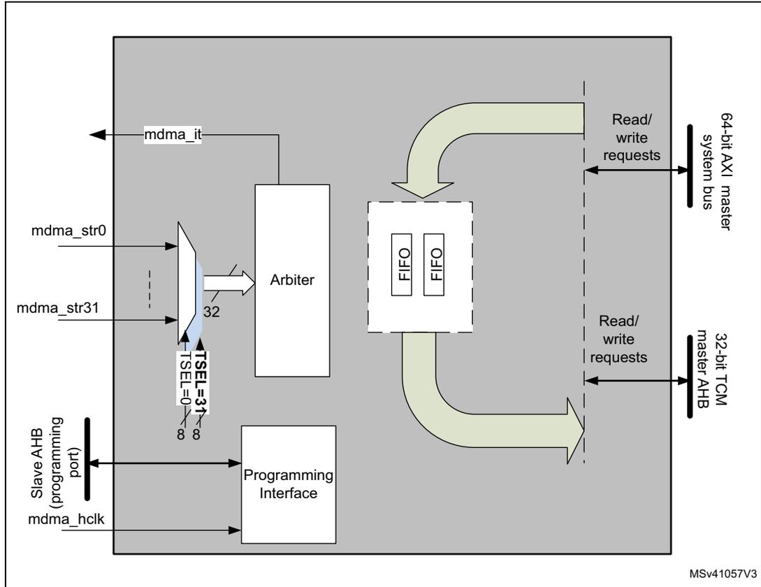
The block diagram illustrates the internal architecture of the MDMA controller. On the left, a 'Slave AHB (programming port)' is connected to a 'Programming Interface'. This interface receives 'mdma_hclk' and 'mdma_str[0:31]' signals. The 'mdma_str' signals pass through a multiplexer (labeled 'TSEL=31' and 'TSEL=0') and then to an 'Arbiter'. The 'Arbiter' outputs an 'mdma_it' (interrupt) signal. The 'Arbiter' also connects to a 'FIFO' block containing two FIFOs. These FIFOs are connected to two master interfaces on the right: a '64-bit AXI master system bus' and a '32-bit TCM master AHB'. Both interfaces receive 'Read/write requests' from the FIFOs. The diagram is labeled 'MSv41057V3' in the bottom right corner.
14.3.2 MDMA internal signals
The table below shows the internal MDMA signals.
Table 104. MDMA internal input/output signals
| Signal name | Signal type | Description |
|---|---|---|
| mdma_hclk | Digital input | MDMA AHB clock |
| mdma_it | Digital output | MDMA interrupt |
| mdma_str[0:31] | Digital input | MDMA stream request |
14.3.3 MDMA overview
The MDMA performs a direct memory transfer: as an AXI/AHB master, the MDMA can take the control of the AXI/AHB bus matrix to initiate AXI/AHB transactions.
The MDMA can carry out the following transactions:
- • memory-to-memory (software triggered)
- • peripheral-to-memory
- • memory-to-peripheral
For the last two transaction types, the memory can also be replaced by a memory-mapped peripheral, which has no control over the MDMA flow. When these types of transaction are used and the request comes from a standard DMA (DMA1 or DMA2), the peripheral register access is replaced by a memory access to the memory buffer used by this DMA.
Note: Non-incrementing/decrementing mode is not used for memory accesses.
The source and destination are simply defined by the address (peripherals being memory-mapped also).
The AHB slave port is used to program the MDMA (it supports 8-, 16-, and 32-bit accesses).
The size of the data array to be transferred for a single request is one of the following:
- • buffer transfer size
- • block size
- • repeated block
- • complete channel data (until the linked-list pointer for the channel is null)
The choice of the size is done through the TRGM[1:0] (Trigger mode) selection field.
The user must choose one of them based on the data array size available (usually in the DMA1/2 memory buffer) and the “real time” requirements for other MDMA channels (knowing that a buffer transfer is the minimum data aggregate to be transferred by the MDMA without doing a new arbitration between MDMA channel requests).
For each channel, there are three key data array sizes:
- • Burst size: this is the length of the data transfer which can be performed in burst mode. This burst length defines the maximum transfer length which cannot be interrupted at bus arbitration level and can block other masters from accessing the bus.
- • Buffer transfer size: this is the length of the data array to be transferred, on a channel, before checking for MDMA requests on other channels. This is the data array transfer lengths which cannot be interrupted at MDMA level (from other channel requests).
- • Block size: this value has two meanings which can be used together:
- – main: this is length of the data block which is described in a block structure of the MDMA linked list (corresponds to one entry in the linked list)
- – selectable: when TRGM[1:0] equals 01, this is the length of the data array which is transferred on a single MDMA request activation (for the respective channel)
14.3.4 MDMA channel
Each MDMA channel provides an unidirectional transfer link between a source and a destination.
Each channel can perform transfer of the following types:
- • Single block transfer: one block is transferred. At the end of the block, the MDMA channel is disabled and an end-of-channel transfer interrupt is generated.
- • Repeated block transfer: a number of blocks is transferred before disabling the channel.
- • Linked-list transfer: when the transfer of the current data block (or last block in a repeat) is completed, a new block control structure is loaded from memory and a new block transfer is started.
The minimum amount of data to be transferred for each request (buffer size, up to 128 bytes) is programmable. The total amount of data in a block, is programmable up to 64 Kbytes. This value is decremented after each transfer. When this counter reaches zero, the end of the block is reached and an action is taken based on the repeat counter (for repeated block transfer) and/or linked-list structure value.
Note: If the block length is not a multiple of the buffer length, the last buffer transfer in the block is shorter, covering the remaining bytes to be transferred in the current block.
If the link structure address points to a valid memory address, the MDMA reloads the whole channel descriptor structure register contents from memory at this address. Then, a new block transfer is then executed (on the next MDMA channel request) based on this information.
If the link structure address is 0x0, at the end of the current/repeated block transfer, the MDMA channel is disabled and the end-of-channel transfer interrupt is generated.
14.3.5 Source, destination and transfer modes
Both source and destination transfers can address peripherals and memories in the entire 4-Gbyte area, at addresses comprised between 0x0000 0000 and 0xFFFF FFFF.
The source/destination addresses can be fixed (such as FIFO/single data register peripherals) or incremented/decremented. The transfer can be done in single access or in burst mode (programmable).
14.3.6 Pointer update
The source and destination memory pointers can optionally be automatically post-incremented/decremented, or kept constant after each transfer depending on the SINC[1:0] and DINC[1:0] bitfields in the MDMA_CxCR register.
Disabling the increment mode is useful when the peripheral source or destination data are accessed through a single register/FIFO mode.
If the increment/decrement mode is enabled, the address of the next data transfer is the address of the previous one incremented/decrement by 1, 2, 4 or 8 depending on the increment size programmed in SINCOS[1:0] or DINCOS[1:0] in MDMA_CxCR.
In order to optimize the packing operation, the increment offset size and the data size are programmable independently.
14.3.7 MDMA buffer transfer
This is the minimum logical amount of data (up to 128 bytes) which is transferred on an MDMA request event, on one channel.
An MDMA buffer transfer consists of a sequence of a given number of data transfers (done as single or burst data transfers). The number of data items to be transferred and their width (8, 16, 32, or 64 bits) are software programmable. The length of the burst used for data transfers is also programmable, independently.
After an event requiring a data array to be transferred, the DMA/peripheral sends a request signal to the MDMA, which serves the request depending on the channel priorities.
The request is acknowledged by writing the mask data value to the address given mask address, when these registers are set.
If the mask address register is not set (0x00 value), the request can be reset by simply reading/writing the data to the peripheral. In this case, if the request is done by a destination peripheral, the write must be set as non bufferable, in order to avoid a false new MDMA request.
The total amount of data to be transferred, on the current channel, following a MDMA request, is determined by the TRGM[1:0] field.
If TRGM[1:0] equals 00, a single buffer is transferred, then the MDMA waits for another request on the same channel.
Note: In this case, the hardware request for the currently active channel (data in the FIFO) is not considered again until the end of the write phase for this channel. Even if the channel is still active at the end of the read phase, another channel (even with lower priority) can start the read phase. Lower priority channels can be interleaved with current channel transfer.
If TRGM[1:0] is different from 00 (multiple buffers need to be transferred), the
mdma_strx
for the current channel remains active (internally memorized) until the whole transfer defined by TRGM (block, repeated block or whole channel/linked list data) is completed.
After transferring an individual buffer, the MDMA enters in a new arbitration phase (between new external requests and internally memorized ones). If no other higher priority, the channel request is active, and a new buffer transfer is started for the same channel.
Note: When TRGM[1:0] is different from 00, a larger array of data is transferred for a single request. But, as the channel arbitration is done after each buffer transfer, no higher level MDMA requests are blocked for the more than a buffer transfer period, on any lower priority channel.
14.3.8 Request arbitration
An arbiter manages the MDMA channel requests based on their priority. When the MDMA is idle and after the end of each buffer transfer, all MDMA requests (hardware or software) are checked for all enabled channels.
Priorities are managed in two stages:
- • Software: each stream priority can be configured in the MDMA_CxCR register. There are four levels:
- – Very high priority
- – High priority
- – Medium priority
- – Low priority
- • Hardware: at hardware level, the channel priority is fixed. If two requests have the same software priority level, the channel with the lower number takes priority over the stream with the higher number. For example, Channel 2 takes priority over Channel 4 when they have the same software priority level.
14.3.9 FIFO
A FIFO structure is used to temporarily store data coming from the source before writing them to the destination. There is a central FIFO structure which is used for all channels.
In order to maximize data bandwidth and bus usage, the following mechanisms are used, allowing multiple read/write operation to be executed in parallel.
- • During a buffer transfer, as soon as the FIFO contains enough data for a destination burst transfer, the write operation starts.
- • When the complete data for a buffer transfer has been read into the FIFO, the arbitration procedure is started. Following that, the next buffer data to be transferred can be read to the FIFO.
When an active channel is disabled due to an error, during a buffer transfer, the remaining data in the internal FIFO is discarded.
14.3.10 Block transfer
A block is a “contiguous” array of data, up to 64 Kbytes, which is transferred by successive buffer transfers.
Each block of data is defined by the start address and the block length. When a block transfer is completed, one of the following three actions can be executed:
- • The block is part of a repeated block transfer: the block length is reloaded and new block start address is computed (based on the information in MDMA_CxBRUR).
- • It is a single block or the last block in a repeated block transfer: the next block information is loaded from the memory (using the linked list address information, from MDMA_CxLAR).
- • It is the last block which needs to be transferred for the current MDMA channel (MDMA_CxLAR = 0): the channel is disabled and no further MDMA requests are accepted for this channel.
14.3.11 Block repeat mode
The block repeat mode is used to repeat a block transfer, with different start addresses for source and destination.
When the repeat block mode is active (repeat counter \( \neq 0 \) ), at the end of the current block transfer, the block parameters are updated (BNDT value reloaded and SAR/DAR values updated according to BRSUM/BRDUM configuration), and the repeat counter decremented by one.
When the repeat block counter reaches 0, this last block is treated as a single block transfer.
14.3.12 Linked-list mode
The linked-list mode allows a new MDMA configuration to be loaded (MDMA_CxTCR, MDMA_CxBNDTR, MDMA_CxSAR, MDMA_CxDAR, MDMA_CxBRUR, MDMA_CxLAR, MDMA_CxTBR, MDMA_CxMAR and MDMA_CxMDR registers), from the address given in MDMA_CxLAR. This address must address a memory mapped on the AXI system bus.
Following this operation, the channel is ready to accept new requests, as defined in the block/repeated block modes above, or continue the transfer if TRGM[1:0] = 11.
The trigger source can be automatically changed, when loading the MDMA_CxTBR value.
The TRGM and SWRM values must not be changed when TRGM[1:0] = 11.
14.3.13 MDMA transfer completion
Different events can generate an end of transfer by setting the CTCIF bit in the status register (MDMA_CxISR):
- • The MDMA_CxBNDTR counter has reached zero, the Block Repeat Counter is 0 and the Link list pointer address is 0
- • The channel is disabled before the end of transfer (by clearing the EN bit in MDMA_CxCR) and all the remaining data have been transferred from the FIFO to the destination
14.3.14 MDMA transfer suspension
At any time, a MDMA transfer can be suspended in order to be restarted later on or to be definitively disabled before the end of the MDMA transfer.
There are two cases:
- • The channel is disabled, with no later-on restart from the point where it was stopped. There is no particular action to do, besides clearing the EN bit in the MDMA_CxCR register to disable the channel. The stream can take time to be disabled (on going buffer transfer is completed first). The transfer complete interrupt flag is set in order to indicate the end of transfer. The value of the EN bit in MDMA_CxCR is now 0 to confirm the channel interruption. The MDMA_CxNDTR register contains the number of remaining data items when the channel was stopped. The software can then determine how many data items have been transferred before the channel was interrupted.
- • The channel is suspended before the number of remaining bytes to be transferred in the MDMA_CxBNDTR register reaches zero. The aim is to restart the transfer later by re-enabling the channel. The channel transfer complete interrupt flag CTCIF is set in order to indicate the end of transfer. If the MDMA_CxBNDTR, MDMA_CxSAR and
MDMA_CxDAR registers are not modified by software, the transfer continues when the channel is re-enabled. CTCIF must also be reset before restarting the channel.
Note: If the completed buffer is the last of the block, the configuration registers are also updated before disabling the channel, in order to be correctly prepared for a soft restart.
Before reprogramming the channel, the software must wait the MDMA_CTCIF register is set, in order to guarantee that any ongoing operation has been completed.
14.3.15 Error management
The MDMA can detect the following errors and the transfer error interrupt flag (TEIF) is set:
- • when a bus error occurs during a MDMA read/write access
- • when an address alignment does not correspond to the data size
- • when the block size is not a multiple of the data size (for source and/or destination): this error is activated on the last transfer and the error address points to the last transfer (which cannot be done)
14.4 MDMA interrupts
For each MDMA channel, an interrupt can be produced on the following events:
- • Channel transfer completed
- • Block-transfer completed
- • Block-transfer repeat completed
- • Buffer transfer completed
- • Transfer error
Separate interrupt enable control bits are available for flexibility as shown in the table below.
Table 105. MDMA interrupt requests
| Interrupt event | Event flag | Enable control bit |
|---|---|---|
| Channel transfer completed | CTCIF | CTCIE |
| Block-transfer repeat completed | BTRIF | BTRIE |
| Block-transfer completed | BTIF | BTIE |
| Buffer transfer completed | TCIF | TCIE |
| Transfer error | TEIF | TEIE |
Note: Before setting an enable control bit to 1, the corresponding event flag must be cleared, otherwise an interrupt may be immediately generated, if the bit is already set.
When at least one interrupt flag and the respective enable control bit are set, the channel interrupt bit is set in the MDMA_GISR. The interrupt output is also activated. This generates an interrupt if the respective interrupt channel is enabled in the NVIC.
14.5 MDMA registers
The MDMA registers can be accessed in word, half-word, or byte format.
14.5.1 MDMA global interrupt status register (MDMA_GISR0)
Address offset: 0x00
Reset value: 0x0000 0000
| 31 | 30 | 29 | 28 | 27 | 26 | 25 | 24 | 23 | 22 | 21 | 20 | 19 | 18 | 17 | 16 |
|---|---|---|---|---|---|---|---|---|---|---|---|---|---|---|---|
| Res. | Res. | Res. | Res. | Res. | Res. | Res. | Res. | Res. | Res. | Res. | Res. | Res. | Res. | Res. | Res. |
| 15 | 14 | 13 | 12 | 11 | 10 | 9 | 8 | 7 | 6 | 5 | 4 | 3 | 2 | 1 | 0 |
| GIF15 | GIF14 | GIF13 | GIF12 | GIF11 | GIF10 | GIF9 | GIF8 | GIF7 | GIF6 | GIF5 | GIF4 | GIF3 | GIF2 | GIF1 | GIF0 |
| r | r | r | r | r | r | r | r | r | r | r | r | r | r | r | r |
Bits 31:16 Reserved, must be kept at reset value.
Bits 15:0 GIF[15:0] : Channel x global interrupt flag (x = 15 to 0)
This bitfield is set and reset by hardware. It is a logical OR of all channel x interrupt flags (CTCIF, BTIF, BRTIF, TEIF) which are enabled in MDMA_CTCIEx, MDMA_BTIEEx, MDMA_BRTIEEx, and MDMA_TEIEEx.
0: No interrupt generated by channel x
1: Interrupt generated by channel x
14.5.2 MDMA channel x interrupt status register (MDMA_CxISR)
Address offset: 0x40 + 0x40 * x, (x = 0 to 15)
Reset value: 0x0000 0000
| 31 | 30 | 29 | 28 | 27 | 26 | 25 | 24 | 23 | 22 | 21 | 20 | 19 | 18 | 17 | 16 |
|---|---|---|---|---|---|---|---|---|---|---|---|---|---|---|---|
| Res. | Res. | Res. | Res. | Res. | Res. | Res. | Res. | Res. | Res. | Res. | Res. | Res. | Res. | Res. | CRQA |
| 15 | 14 | 13 | 12 | 11 | 10 | 9 | 8 | 7 | 6 | 5 | 4 | 3 | 2 | 1 | 0 |
| Res | Res | Res | Res | Res | Res | Res | Res | Res | Res | Res | TCIF | BTIF | BRTIF | CTCIF | TEIF |
| r | r | r | r | r |
Bits 31:17 Reserved, must be kept at reset value.
Bit 16 CRQA: Channel x request active flagThis bit is set by software writing 1 to SWRQx in MDMA_CxCR, in order to request an MDMA transfer, and the channel x is enabled.
This bit is also set by hardware when the channel request becomes active, and the channel is enabled. The hardware request memorized until it is served.
This bit is cleared by hardware when the channel x request is completed (after the source write phase of the last buffer transfer due for the current request).
0: The MDMA transfer mdma_strx is inactive for channel x.
1: The MDMA transfer mdma_strx is active for channel x
Note: This bit is also reset by hardware when the channel is disabled (in case of transfer error, or when reaching the end of the channel data transfer - repeat block = 0 and linked list pointer null-, or by software programming the channel enable bit to 0 before that).
Bits 15:5 Reserved, must be kept at reset value.
Bit 4 TCIF: Channel x buffer transfer complete interrupt flagThis bit is set by hardware. It is cleared by software writing 1 to the corresponding bit in MDMA_IFCRy.
0: No buffer transfer complete event on channel x
1: A buffer transfer complete event occurred on channel x
TC is set when a single buffer is transferred. It is activated on each channel transfer request.
This can be used as a debug feature (without interrupt), indicating that (at least) an MDMA buffer transfer has been generated since the last flag reset.
Bit 3 BTIF: Channel x block transfer complete interrupt flagThis bit is set by hardware. It is cleared by software writing 1 to the corresponding bit in MDMA_IFCRy.
0: No block transfer complete event on channel x
1: A block transfer complete event occurred on channel x.
Bit 2 BRTIF: Channel x block repeat transfer complete interrupt flagThis bit is set by hardware. It is cleared by software writing 1 to the corresponding bit in MDMA_IFCRy.
0: No block repeat transfer complete event on channel x
1: A block repeat transfer complete event occurred on channel x
Bit 1 CTCIF: Channel x channel transfer complete interrupt flagThis bit is set by hardware. It is cleared by software writing 1 to the corresponding bit in MDMA_IFCRy.
0: No channel transfer complete event on channel x
1: A channel transfer complete event occurred on channel x
CTC is set when the last block was transferred and the channel has been automatically disabled.
CTC is also set when the channel is suspended, as a result of writing EN bit to 0.
Bit 0 TEIF: Channel x transfer error interrupt flagThis bit is set by hardware. It is cleared by software writing 1 to the corresponding bit in MDMA_IFCRy.
0: No transfer error on stream x
1: A transfer error occurred on stream x
14.5.3 MDMA channel x interrupt flag clear register (MDMA_CxIFCR)
Address offset: 0x44 + 0x40 * x, (x = 0 to 15)
Reset value: 0x0000 0000
| 31 | 30 | 29 | 28 | 27 | 26 | 25 | 24 | 23 | 22 | 21 | 20 | 19 | 18 | 17 | 16 |
|---|---|---|---|---|---|---|---|---|---|---|---|---|---|---|---|
| Res. | Res. | Res. | Res. | Res. | Res. | Res. | Res. | Res. | Res. | Res. | Res. | Res. | Res. | Res. | Res. |
| 15 | 14 | 13 | 12 | 11 | 10 | 9 | 8 | 7 | 6 | 5 | 4 | 3 | 2 | 1 | 0 |
| Res. | Res. | Res. | Res. | Res. | Res. | Res. | Res. | Res. | Res. | Res. | CLTCIF | CBTIF | CBRTIF | CCTCIF | CTEIF |
| w | w | w | w | w |
Bits 31:5 Reserved, must be kept at reset value.
Bit 4
CLTCIF
: Clear buffer transfer complete Interrupt flag for channel x
Writing 1 into this bit clears TCIF in MDMA_ISRy.
Bit 3
CBTIF
: Channel x clear block transfer complete interrupt flag
Writing 1 into this bit clears BTIF in MDMA_ISRy.
Bit 2
CBRTIF
: Channel x clear block repeat transfer complete interrupt flag
Writing 1 into this bit clears BRTIF in MDMA_ISRy.
Bit 1
CCTCIF
: Clear channel transfer complete interrupt flag for channel x
Writing 1 into this bit clears CTCIF in MDMA_ISRy.
Bit 0
CTEIF
: Channel x clear transfer error interrupt flag
Writing 1 into this bit clears TEIF in MDMA_ISRy.
14.5.4 MDMA channel x error status register (MDMA_CxESR)
Address offset: 0x48 + 0x40 * x, (x = 0 to 15)
Reset value: 0x0000 0000
| 31 | 30 | 29 | 28 | 27 | 26 | 25 | 24 | 23 | 22 | 21 | 20 | 19 | 18 | 17 | 16 |
|---|---|---|---|---|---|---|---|---|---|---|---|---|---|---|---|
| Res. | Res. | Res. | Res. | Res. | Res. | Res. | Res. | Res. | Res. | Res. | Res. | Res. | Res. | Res. | Res. |
| 15 | 14 | 13 | 12 | 11 | 10 | 9 | 8 | 7 | 6 | 5 | 4 | 3 | 2 | 1 | 0 |
| Res. | Res. | Res. | Res. | BSE | ASE | TEMD | TELD | TED | TEA[6:0] | ||||||
| r | r | r | r | r | r | r | r | r | r | r | r | ||||
Bits 31:12 Reserved, must be kept at reset value.
Bit 11 BSE : Block size error
This bit is set by hardware, when the block size is not an integer multiple of the data size either for source or destination. TED indicates whether the problem is on the source or destination. This bit is cleared by software writing 1 to CTEIF in MDMA_IFCRy.
0: No block size error
1: Programmed block size is not an integer multiple of the data size.
Bit 10 ASE : Address size error
This bit is set by hardware, when the programmed address is not aligned with the data size. TED indicates whether the problem is on the source or destination. It is cleared by software writing 1 to CTEIF in MDMA_IFCRy.
0: No address size error
1: Programmed address is not coherent with the data size.
Bit 9 TEMD : Transfer error mask data
This bit is set by hardware, in case of a transfer error while writing the mask data. It is cleared by software writing 1 to CTEIF in MDMA_IFCRy.
0: No mask write access error
1: The last transfer error on the channel was a related to a write of the mask data.
Bit 8 TELD : Transfer error link data
This bit is set by hardware, in case of a transfer error while reading the block link data structure. It is cleared by software writing 1 to CTEIF in MDMA_IFCRy.
0: No link data read access error
1: The last transfer error on the channel was a related to a read of the link data structure.
Bit 7 TED : Transfer error direction
This bit is set and cleared by hardware, in case of an MDMA data transfer error.
0: The last transfer error on the channel was a related to a read access.
1: The last transfer error on the channel was a related to a write access.
Bits 6:0 TEA[6:0] : Transfer error address
These bits are set and cleared by hardware in case of an MDMA data transfer error. They are used in conjunction with TED. This field indicates the 7 LSB bits of the address which generated a transfer/access error.
This field can be used by software to retrieve the failing address, by adding this value (truncated to the buffer transfer length size) to the current SAR/DAR value.
Note: The SAR/DAR current value does not reflect this last address due to the FIFO management system. The SAR/DAR are only updated at the end of a (buffer) transfer (of TLEN+1 bytes).
This field is not set in case of a link data error.
14.5.5 MDMA channel x control register (MDMA_CxCR)
This register is used to control the concerned channel.
Address offset: 0x4C + 0x40 * x, (x = 0 to 15)
Reset value: 0x0000 0000
| 31 | 30 | 29 | 28 | 27 | 26 | 25 | 24 | 23 | 22 | 21 | 20 | 19 | 18 | 17 | 16 |
|---|---|---|---|---|---|---|---|---|---|---|---|---|---|---|---|
| Res. | Res. | Res. | Res. | Res. | Res. | Res. | Res. | Res. | Res. | Res. | Res. | Res. | Res. | Res. | SWRQ |
| w | |||||||||||||||
| 15 | 14 | 13 | 12 | 11 | 10 | 9 | 8 | 7 | 6 | 5 | 4 | 3 | 2 | 1 | 0 |
| Res. | WEX | HEX | BEX | Res. | Res. | Res. | Res. | PL[1:0] | TCIE | BTIE | BRTIE | CTCIE | TEIE | EN | |
| rw | rw | rw | rw | rw | rw | rw | rw | rw | rw | rw |
Bits 31:17 Reserved, must be kept at reset value.
Bit 16 SWRQ : Software request
Writing 1 into this bit sets the CRQA in MDMA_ISRy, activating the request on channel x.
Note: Either the whole MDMA_CxCR register or the 8-/16-bit register at the address offset: \( 0x4E + 0x40 \times \text{channel number} \) , can be used for SWRQ activation.
In case of software request, acknowledge is not generated (neither hardware signal, nor MDMA_CxMAR write access).
Bit 15 Reserved, must be kept at reset value.
Bit 14 WEX : Word endianness exchange
This bit is set and cleared by software.
- 0: Little endianness preserved for words
- 1: Word order exchanged in double word
When this bit is set, the word order in the destination double word is reversed: higher address word contains the data read from the lower address of the source.
If the destination is not a double word, do not care of this bit value.
Note: This bit is protected and can be written only if EN is 0.
Bit 13 HEX : Half-word endianness exchange
This bit is set and cleared by software.
- 0: Little endianness preserved for half words
- 1: half-word order exchanged in each word
When this bit is set, the half-word order in each destination word is reversed: higher address half-word contains the data read from the lower address of the source.
If destination length is shorter than word, do not care of this bit value.
Note: This bit is protected and can be written only if EN is 0.
Bit 12 BEX : Byte endianness exchange
This bit is set and cleared by software.
- 0: Little endianness preserved for bytes
- 1: byte order exchanged in each half-word
When this bit is set, the byte order in each destination half-word is reversed: higher address word contains the data read from the lower address of the source.
If destination is byte, do not care of this bit value.
Note: This bit is protected and can be written only if EN is 0.
Bits 11:9 Reserved, must be kept at reset value.
Bit 8 Reserved, must be kept at reset value.
Bits 7:6 PL[1:0] : Priority level
These bits are set and cleared by software.
- 00: Low
- 01: Medium
- 10: High
- 11: Very high
Note: These bits are protected and can be written only if EN is 0.
Bit 5 TCIE : Buffer transfer complete interrupt enable
This bit is set and cleared by software.
- 0: TC interrupt disabled
- 1: TC interrupt enabled
Bit 4 BTIE : Block transfer interrupt enable
This bit is set and cleared by software.
0: BT complete interrupt disabled
1: BT complete interrupt enabled
Bit 3 BRTIE : Block repeat transfer interrupt enable
This bit is set and cleared by software.
0: BT interrupt disabled
1: BT interrupt enabled
Bit 2 CTCIE : Channel transfer complete interrupt enable
This bit is set and cleared by software.
0: TC interrupt disabled
1: TC interrupt enabled
Bit 1 TEIE : Transfer error interrupt enable
This bit is set and cleared by software.
0: TE interrupt disabled
1: TE interrupt enabled
Bit 0 EN : Channel enable/flag channel ready when read low
This bit is set and cleared by software.
0: Channel disabled
1: Channel enabled
This bit can be cleared by hardware:
- – on a MDMA end of transfer (stream ready to be configured)
- – if a transfer error occurs on the AHB/AXI master buses (bus error/HardFault)
- – if another error condition is encountered (data alignment, block/data size incompatibility)
When this bit is reset by software, the ongoing buffer transfer (if any) is completed.
All status/configuration registers keep their current values. If the channel is re-enabled without writing these registers, the channel continues from the point where it was interrupted.
When this bit is read as 0, the software is allowed to program the configuration registers.
It is forbidden to write these registers when the EN bit is read as 1 (writes are ignored).
Note: When this bit is reset by software, it is recommended to wait for the CTCIF = 1, in order to ensure that any ongoing buffer transfer has been completed, before reprogramming the channel.
14.5.6 MDMA channel x transfer configuration register (MDMA_CxTCR)
Address offset: 0x50 + 0x40 * x, (x = 0 to 15)
Reset value: 0x0000 0000
This register is used to configure the concerned channel. In linked-list mode, at the end of a block (single or last block in repeated block transfer mode), this register is loaded from the memory (from address given by current LAR[31:0] + 0x00).
| 31 | 30 | 29 | 28 | 27 | 26 | 25 | 24 | 23 | 22 | 21 | 20 | 19 | 18 | 17 | 16 |
|---|---|---|---|---|---|---|---|---|---|---|---|---|---|---|---|
| BWM | SWRM | TRGM[1:0] | PAM[1:0] | PKE | TLEN[6:0] | DBURST[2:1] | |||||||||
| rw | rw | rw | rw | rw | rw | rw | rw | rw | rw | rw | rw | rw | rw | rw | rw |
| 15 | 14 | 13 | 12 | 11 | 10 | 9 | 8 | 7 | 6 | 5 | 4 | 3 | 2 | 1 | 0 |
| DBURST[0] | SBURST[2:0] | DINCOS[1:0] | SINCOS[1:0] | DSIZE[1:0] | SSIZE[1:0] | DINC[1:0] | SINC[1:0] | ||||||||
| rw | rw | rw | rw | rw | rw | rw | rw | rw | rw | rw | rw | rw | rw | rw | rw |
This bit is set and cleared by software.
0: The destination write operation is non-bufferable.
1: The destination write operation is bufferable.
Note: This bit is protected and can be written only if EN is 0.
All MDMA destination accesses are non-cacheable.
Bit 30 SWRM: Software request modeThis bit is set and cleared by software. If an hardware or software request is currently active, the bit change is delayed until the current transfer is completed.
0: Hardware request are taken into account: the transfer is initiated as defined by TRGM value and acknowledged by the MDMA_ACKx signal. If the MDMA_CxMAR contains a valid address, the MDMA_CxMDR value is also written at MDMA_CxMAR address.
1: Hardware request are ignored. Transfer is triggered by software writing 1 to the SWRQ bit.
Note: This bit is protected and can be written only if EN is 0.
Bits 29:28 TRGM[1:0]: Trigger modeThese bits are set and cleared by software.
00: Each MDMA request (software or hardware) triggers a buffer transfer.
01: Each MDMA request (software or hardware) triggers a block transfer.
10: Each MDMA request (software or hardware) triggers a repeated block transfer (if the block repeat is 0, a single block is transferred).
11: Each MDMA request (software or hardware) triggers the transfer of the whole data for the respective channel (for example linked list) until the channel reach the end and it is disabled.
Note: If TRGM is 11 for the current block, all values loaded at the end of the current block through the linked-list mechanism must keep the same value (TRGM = 11), and the same SWRM value, otherwise the result is undefined.
These bits are protected and can be written only if EN is 0.
Bits 27:26 PAM[1:0]: Padding/alignment modeThese bits are set and cleared by software.
00: Right aligned, padded with 0s (default). If source data is larger than destination size, only LSB part of the source is written to the destination address. The reminder part is discarded.
01: Right aligned, sign extended
10: Left aligned (padded with 0s). if source data is larger than destination size, only MSB part of the source is written to the destination address. The reminder part is discarded.
11: Reserved
Note: When PKE = 1 or DSIZE=SSIZE, these bits are ignored.
These bits are protected and can be written only if EN is 0.
Bit 25 PKE: Pack enableThis bit is set and cleared by software.
0: The source data is written to the destination as is. If source size is smaller than destination, it is padded according to the PAM value. If source data size is larger than destination one, it is truncated. The alignment is done according to the PAM[1:0] value.
1: The source data is packed/unpacked into the destination data size. All data are right aligned, in little-endian mode.
Note: This bit is protected and can be written only if EN is 0.
Bits 24:18 TDLEN[6:0] : Buffer transfer length (number of bytes - 1)
These bits are set and cleared by software. TDLEN + 1 value represents the number of bytes to be transferred in a single transfer.
The transfer length must be a multiple of the data size (for both source and destination)
When the source/destination sizes are different and padding/truncation is used, TDLEN + 1 refers to the source data array size.
Note: These bits are protected and can be written only if EN is 0.
DBURST value must be programmed in order to ensure that the burst size is lower than the transfer size.
Bits 17:15 DBURST[2:0] : Destination burst transfer configuration
These bits are set and cleared by software.
000: Single transfer
N: burst of \( 2^N \) beats
DBURST value must be programmed as to ensure that the burst size is lower than the transfer length. If this is not ensured, the result is unpredictable.
Note: These bits are protected and can be written only if EN is 0.
When the destination bus is TCM/AHB (DBUS = 1) and DINCOS = 11 or DINC = 00 or DINCOS ≠ DSIZE, DBURST must be programmed to 000 (single transfer), else the result is unpredictable.
When the destination bus is system/AXI bus (DBUS = 0) and DINC = 00, DBURST must be maximum 100 (burst of 16), else the result is unpredictable.
Bits 14:12 SBURST[2:0] : Source burst transfer configuration
These bits are set and cleared by software.
000: single transfer
N: burst of \( 2^N \) beats
SBURST value must be programmed as to ensure that the burst size is lower than the transfer length. If this is not ensured, the result is unpredictable.
Note: These bits are protected and can be written only if EN is 0.
When the source bus is TCM (SBUS = 1) and SINCOS = 11 or SINC = 00 or SINCOS ≠ SSIZE, SBURST must be programmed to 000 (single transfer), else the result is unpredictable.
When the source bus is system/AXI bus (SBUS = 0) and SINC = 00, SBURST must be maximum 100 (burst of 16), else the result is unpredictable.
Bits 11:10 DINCOS[1:0] : Destination increment offset size
These bits are set and cleared by software.
00: byte (8-bit)
01: half-word (16-bit)
10: word (32-bit)
11: Double-Word (64-bit) -
This bits have no meaning if bit DINC[1:0] = 00.
Note: If DINCOS < DSIZE and DINC ≠ 00, the result is unpredictable.
If destination is AHB and DBURST ≠ 000, destination address must be aligned with DINCOS size, else the result is unpredictable.
These bits are protected and can be written only if EN = 0.
Bits 9:8 SINCOS[1:0] : Source increment offset size
These bits are set and cleared by software.
00: byte (8-bit)
01: half-word (16-bit)
10: word (32-bit)
11: Double-Word (64-bit) -
This bits have no meaning if bit SINC[1:0] = 00.
Note: If SINCOS < SSIZE and SINC ≠ 00, the result is unpredictable.
If source is TCM/AHB and SBURST ≠ 000, source address must be aligned with SINCOS size, else the result is unpredictable.
These bits are protected and can be written only if EN = 0.
Bits 7:6 DSIZE[1:0] : Destination data size
These bits are set and cleared by software.
00: Byte (8 bits)
01: Half-word (16 bits)
10: Word (32 bits)
11: Double-word (64 bits)
Note: If DINCOS < DSIZE and DINC ≠ 00, the result is unpredictable.
If a value of 11 is programmed for the TCM access/AHB port, a transfer error occurs (TEIF bit set). DSIZE = 11 (double-word) is forbidden when destination is TCM/AHB bus (DBUS = 1).
These bits are protected and can be written only if EN = 0.
Bits 5:4 SSIZE[1:0] : Source data size
These bits are set and cleared by software.
00: Byte (8 bits)
01: Half-word (16 bits)
10: Word (32 bits)
11: Double-word (64 bits)
Note: If SINCOS < SSIZE and SINC ≠ 00, the result is unpredictable.
If a value of 11 is programmed for the TCM access/AHB port, a transfer error occurs (TEIF bit set). SSIZE = 11 (double-word) is forbidden when source is TCM/AHB bus (SBUS = 1).
These bits are protected and can be written only if EN is 0.
Bits 3:2 DINC[1:0] : Destination increment mode
These bits are set and cleared by software.
00: Destination address pointer is fixed.
10: Destination address pointer is incremented after each data transfer (increment is done according to DINCOS).
11: Destination address pointer is decremented after each data transfer (increment is done according to DINCOS).
Note: These bits are protected and can be written only if EN = 0.
When destination is AHB (DBUS = 1), DINC = 00 is forbidden.
Bits 1:0 SINC[1:0] : Source increment mode
These bits are set and cleared by software.
00: Source address pointer is fixed.
10: Source address pointer is incremented after each data transfer (increment is done according to SINCOS).
11: Source address pointer is decremented after each data transfer (decrement is done according to SINCOS).
Note: These bits are protected and can be written only if EN = 0.
When source is AHB (SBUS = 1), SINC = 00 is forbidden.
14.5.7 MDMA channel x block number of data register (MDMA_CxBNDTR)
Address offset: 0x54 + 0x40 * x, (x = 0 to 15)
Reset value: 0x0000 0000
In linked-list mode, at the end of a block (single or last block in repeated block transfer mode), this register is loaded from the memory (from address given by current LAR[31:0] + 0x04).
| 31 | 30 | 29 | 28 | 27 | 26 | 25 | 24 | 23 | 22 | 21 | 20 | 19 | 18 | 17 | 16 |
|---|---|---|---|---|---|---|---|---|---|---|---|---|---|---|---|
| BRC[11:0] | BRD UM | BRS UM | Res. | BNDT [16] | |||||||||||
| rw | rw | rw | rw | rw | rw | rw | rw | rw | rw | rw | rw | rw | rw | rw | |
| 15 | 14 | 13 | 12 | 11 | 10 | 9 | 8 | 7 | 6 | 5 | 4 | 3 | 2 | 1 | 0 |
| BNDT[15:0] | |||||||||||||||
| rw | rw | rw | rw | rw | rw | rw | rw | rw | rw | rw | rw | rw | rw | rw | rw |
Bits 31:20 BRC[11:0] : Block repeat count
This field contains the number of repetitions of the current block (0 to 4095). When the channel is enabled, this register is read-only, indicating the remaining number of blocks, excluding the current one. This register decrements after each complete block transfer.
Once the last block transfer has completed, this register can either stay at zero or be reloaded automatically from memory (in linked-list mode, meaning link address valid).
Note: These bits are protected and can be written only if EN = 0.
Bit 19 BRDUM : Block repeat destination address update mode
0: At the end of a block transfer, the MDMA_DAR register is updated by adding the DUV to the current DAR value (current destination address).
1: At the end of a block transfer, the MDMA_DAR register is updated by subtracting the DUV from the current DAR value (current destination address).
Note: These bits are protected and can be written only if EN = 0.
Bit 18 BRSUM : Block repeat source address update mode
0: At the end of a block transfer, the MDMA_SAR register is updated by adding the SUV to the current SAR value (current source address).
1: At the end of a block transfer, the MDMA_SAR register is updated by subtracting the SUV from the current SAR value (current source address).
Note: These bits are protected and can be written only if EN = 0.
Bit 17 Reserved, must be kept at reset value.
Bits 16:0 BNDT[16:0] : Block number of data bytes to transfer
Number of bytes to be transferred (0 up to 65536) in the current block. When the channel is enabled, this register is read-only, indicating the remaining data items to be transmitted.
During the channel activity, this register decrements, indicating the number of data items remaining in the current block.
Once the block transfer has completed, this register can either stay at zero or be reloaded automatically with the previously programmed value if the channel is configured in block repeat mode.
If the value of this register is zero, no transaction can be served even if the stream is enabled.
Note: If the BNDT value is not an integer multiple of the TLEN + 1 value, the last transfer is shorter and contains only the remaining data in the block.
The block size must be a multiple of the source and destination data size. If this is not true, an error is set and the no data are written
These bits are protected and can be written only if EN = 0.
14.5.8 MDMA channel x source address register (MDMA_CxSAR)
Address offset: 0x58 + 0x40 * x, (x = 0 to 15)
Reset value: 0x0000 0000
In linked-list mode, at the end of a block (single or last block in repeated block transfer mode), this register is loaded from memory (from address given by current LAR[31:0] + 0x08).
| 31 | 30 | 29 | 28 | 27 | 26 | 25 | 24 | 23 | 22 | 21 | 20 | 19 | 18 | 17 | 16 |
|---|---|---|---|---|---|---|---|---|---|---|---|---|---|---|---|
| SAR[31:16] | |||||||||||||||
| rw | rw | rw | rw | rw | rw | rw | rw | rw | rw | rw | rw | rw | rw | rw | rw |
| 15 | 14 | 13 | 12 | 11 | 10 | 9 | 8 | 7 | 6 | 5 | 4 | 3 | 2 | 1 | 0 |
| SAR[15:0] | |||||||||||||||
| rw | rw | rw | rw | rw | rw | rw | rw | rw | rw | rw | rw | rw | rw | rw | rw |
Bits 31:0 SAR[31:0] : Source address
These bits represent the base address of the peripheral data register from/to which the data is read. They must be aligned with the SSIZE (SAR[1:0] = 00 when SSIZE = 10), but may be unaligned with the SINCOS.
When source is TCM/AHB, if address is not aligned with SINCOS, the access must be programmed as single (SBURST = 000).
During the channel activity, this register is updated, reflecting the current address from which the data is read next.
When the block repeat mode is active, when a block transfer is completed, the source address is updated by adding/subtracting the SAU value to the current value (already updated after the last transfer in the block).
When the linked-list mode is active, at the end of a block (repeated or not) transfer, the SAR value is loaded from memory (from address LSA + m).
Note: These bits are write-protected and can be written only when bit EN = 0.
14.5.9 MDMA channel x destination address register (MDMA_CxDAR)
Address offset: 0x5C + 0x40 * x, (x = 0 to 15)
Reset value: 0x0000 0000
In linked-list mode, at the end of a block (single or last block in repeated block transfer mode), this register is loaded from memory (from address given by current LAR[31:0] + 0x0C).
| 31 | 30 | 29 | 28 | 27 | 26 | 25 | 24 | 23 | 22 | 21 | 20 | 19 | 18 | 17 | 16 |
|---|---|---|---|---|---|---|---|---|---|---|---|---|---|---|---|
| DAR[31:16] | |||||||||||||||
| rw | rw | rw | rw | rw | rw | rw | rw | rw | rw | rw | rw | rw | rw | rw | rw |
| 15 | 14 | 13 | 12 | 11 | 10 | 9 | 8 | 7 | 6 | 5 | 4 | 3 | 2 | 1 | 0 |
| DAR[15:0] | |||||||||||||||
| rw | rw | rw | rw | rw | rw | rw | rw | rw | rw | rw | rw | rw | rw | rw | rw |
Bits 31:0 DAR[31:0] : Destination address
Base address of the destination address to which the data is written. Must be aligned with the DSIZE (for example DAR[0] = 0 when DSIZE=01), but may be unaligned with the DINCOS.
When destination is AHB, if address is not aligned with DINCOS, access must be programmed as single (DBURST = 000).
During the channel activity, this register is updated, reflecting the current address to which the data is written next.
When the block repeat mode is active, when a block transfer is completed, the Destination address is updated by adding/subtracting the DAU value to the current value (after the last transfer in the block).
When the linked-list mode is active, at the end of a block (repeated or not) transfer, the DAR value is loaded from memory (from address LSA + m).
Note: These bits are write-protected and can be written only when bit EN = 0.
14.5.10 MDMA channel x block repeat address update register (MDMA_CxBRUR)
Address offset: 0x60 + 0x40 * x, (x = 0 to 15)
Reset value: 0x0000 0000
In linked-list mode, at the end of a block (single or last block in repeated block transfer mode), this register is loaded from memory (from address given by current LAR[31:0] + 0x10).
| 31 | 30 | 29 | 28 | 27 | 26 | 25 | 24 | 23 | 22 | 21 | 20 | 19 | 18 | 17 | 16 |
|---|---|---|---|---|---|---|---|---|---|---|---|---|---|---|---|
| DUV[15:0] | |||||||||||||||
| rw | rw | rw | rw | rw | rw | rw | rw | rw | rw | rw | rw | rw | rw | rw | rw |
| 15 | 14 | 13 | 12 | 11 | 10 | 9 | 8 | 7 | 6 | 5 | 4 | 3 | 2 | 1 | 0 |
| SUV[15:0] | |||||||||||||||
| rw | rw | rw | rw | rw | rw | rw | rw | rw | rw | rw | rw | rw | rw | rw | rw |
Bits 31:16 DUV[15:0] : Destination address update value
This value is used to update (by addition or subtraction) the current destination address at the end of a block transfer. It must be an integer multiple of DSIZE, in order to keep DAR aligned to DSIZE (DAR[1:0] = 00 when DSIZE = 10).
If this value is 0, the next repetition of the block transfer continues to the next address.
When the block repeat mode is not active (BRC = 0), this field is ignored.
Note: These bits are write-protected and can be written only when bit EN = 0.
This field must be programmed to 0 when \( DINC[1:0] = 00 \) .
Bits 15:0 SUV[15:0] : Source address update value
This value is used to update (by addition or subtraction) the current source address at the end of a block transfer. It must be an integer multiple of SSIZE, in order to keep SAR aligned to SSIZE (SAR[1:0] = 00 when SSIZE = 10).
If this value is 0, the next repetition of the block transfer continues from the next address.
When the block repeat mode is not active (BRC=0), this field is ignored.
Note: These bits are write-protected and can be written only when bit EN = 0.
This field must be programmed to 0 when \( SINC[1:0] = 00 \) .
14.5.11 MDMA channel x link address register (MDMA_CxLAR)
Address offset: 0x64 + 0x40 * x, (x = 0 to 15)
Reset value: 0x0000 0000
In linked-list mode, at the end of a block (single or last block in repeated block transfer mode), this register is loaded from memory (from address given by current LAR[31:0] + 0x14).
Note: The new value is only taken into account after all registers are updated, for the next end of block.
| 31 | 30 | 29 | 28 | 27 | 26 | 25 | 24 | 23 | 22 | 21 | 20 | 19 | 18 | 17 | 16 |
| LAR[31:16] | |||||||||||||||
| rw | rw | rw | rw | rw | rw | rw | rw | rw | rw | rw | rw | rw | rw | rw | rw |
| 15 | 14 | 13 | 12 | 11 | 10 | 9 | 8 | 7 | 6 | 5 | 4 | 3 | 2 | 1 | 0 |
| LAR[15:0] | |||||||||||||||
| rw | rw | rw | rw | rw | rw | rw | rw | rw | rw | rw | rw | rw | r | r | r |
Bits 31:0 LAR[31:0] : Link address register
At the end of a (repeated) block transfer, the current channel configuration registers (MDMA_CxTCR, MDMA_CxBNDTR, MDMA_CxSAR, MDMA_CxDAR, MDMA_CxBRUR, MDMA_CxMAR, MDMA_CxMDR and MDMA_CxLAR itself) are loaded with the data structure found at this address.
If the value of this register is 0, no register update takes place, the channel is disabled and CTCIF is set, indicating the end of the transfer for this channel.
The channel configuration (LAR address) must be in the AXI address space.
LAR value must be aligned at a double-word address ( \( LAR[2:0] = 0x0 \) ).
Note: These bits are write-protected and can be written only when bit EN = 0.
14.5.12 MDMA channel x trigger and bus selection register (MDMA_CxTBR)
Address offset: 0x68 + 0x40 * x, (x = 0 to 15)
Reset value: 0x0000 0000
In linked-list mode, at the end of a block (single or last block in repeated block transfer mode), this register is loaded from memory (from address given by current LAR[31:0] + 0x18).
| 31 | 30 | 29 | 28 | 27 | 26 | 25 | 24 | 23 | 22 | 21 | 20 | 19 | 18 | 17 | 16 |
|---|---|---|---|---|---|---|---|---|---|---|---|---|---|---|---|
| Res. | Res. | Res. | Res. | Res. | Res. | Res. | Res. | Res. | Res. | Res. | Res. | Res. | Res. | DBUS | SBUS |
| 15 | 14 | 13 | 12 | 11 | 10 | 9 | 8 | 7 | 6 | 5 | 4 | 3 | 2 | 1 | 0 |
| Res. | Res. | Res. | Res. | Res. | Res. | Res. | Res. | Res. | Res. | ||||||
| rw | rw | rw | rw | rw | rw |
Bits 31:18 Reserved, must be kept at reset value.
Bit 17 DBUS : Destination bus select
0: The system/AXI bus is used as destination (write operation) on channel x.
1: The AHB bus/TCM is used as destination (write operation) on channel x.
Note: This bit is protected and can be written only if EN is 0.
Bit 16 SBUS : Source bus select
0: The system/AXI bus is used as source (read operation) on channel x.
1: The AHB bus/TCM is used as source (read operation) on channel x.
Note: This bit is protected and can be written only if EN is 0.
Bits 15:6 Reserved, must be kept at reset value.
Bits 5:0 TSEL[5:0] : Trigger selection
This field selects the hardware trigger (RQ) input for channel x. The ACK is sent on the ACK output having the same index value.
When SWRM bit is set (software request selected), this field is ignored.
Note: These bits are write-protected and can be written only when bit EN = 0.
If multiple channels are triggered by the same event (have the same TSEL value), all of them are triggered in parallel. Only the channel with the lowest index acknowledges the request.
14.5.13 MDMA channel x mask address register (MDMA_CxMAR)
Address offset: \( 0x70 + 0x40 * x \) , ( \( x = 0 \) to \( 15 \) )
Reset value: 0x0000 0000
In linked-list mode, at the end of a block (single or last block in repeated block transfer mode), this register is loaded from memory (from address given by current LAR[31:0] + 0x20).
| 31 | 30 | 29 | 28 | 27 | 26 | 25 | 24 | 23 | 22 | 21 | 20 | 19 | 18 | 17 | 16 |
|---|---|---|---|---|---|---|---|---|---|---|---|---|---|---|---|
| MAR[31:16] | |||||||||||||||
| rw | rw | rw | rw | rw | rw | rw | rw | rw | rw | rw | rw | rw | rw | rw | rw |
| 15 | 14 | 13 | 12 | 11 | 10 | 9 | 8 | 7 | 6 | 5 | 4 | 3 | 2 | 1 | 0 |
| MAR[15:0] | |||||||||||||||
| rw | rw | rw | rw | rw | rw | rw | rw | rw | rw | rw | rw | rw | rw | rw | rw |
Bits 31:0 MAR[31:0] : Mask address
A write of the MDR value is also done to this address. This is used to clear the RQ signal generated by the DMA2 by writing to its interrupt clear register.
If the value of this register is 0, this function is disabled.
Note: These bits are write-protected and can be written only when bit EN = 0.
14.5.14 MDMA channel x mask data register (MDMA_CxMDR)
Address offset: \( 0x74 + 0x40 * x \) , ( \( x = 0 \) to \( 15 \) )
Reset value: 0x0000 0000
In Linked List mode, at the end of a block (single or last block in repeated block transfer mode), this register is loaded from memory (from address given by current LAR[31:0] + 0x24).
| 31 | 30 | 29 | 28 | 27 | 26 | 25 | 24 | 23 | 22 | 21 | 20 | 19 | 18 | 17 | 16 |
|---|---|---|---|---|---|---|---|---|---|---|---|---|---|---|---|
| MDR[31:16] | |||||||||||||||
| rw | rw | rw | rw | rw | rw | rw | rw | rw | rw | rw | rw | rw | rw | rw | rw |
| 15 | 14 | 13 | 12 | 11 | 10 | 9 | 8 | 7 | 6 | 5 | 4 | 3 | 2 | 1 | 0 |
| MDR[15:0] | |||||||||||||||
| rw | rw | rw | rw | rw | rw | rw | rw | rw | rw | rw | rw | rw | rw | rw | rw |
Bits 31:0 MDR[31:0] : Mask data
A write of the MDR value is also done to the address defined by the MDMA_MAR register. This is used to clear the RQ signal generated by the DMA2 by writing to its interrupt clear register.
Note: These bits are write-protected and can be written only when bit EN = 0.
14.5.15 MDMA register map
Table 106. MDMA register map and reset values
| Offset | Register name | 31 | 30 | 29 | 28 | 27 | 26 | 25 | 24 | 23 | 22 | 21 | 20 | 19 | 18 | 17 | 16 | 15 | 14 | 13 | 12 | 11 | 10 | 9 | 8 | 7 | 6 | 5 | 4 | 3 | 2 | 1 | 0 |
|---|---|---|---|---|---|---|---|---|---|---|---|---|---|---|---|---|---|---|---|---|---|---|---|---|---|---|---|---|---|---|---|---|---|
| 0x00 | MDMA_GISR0 | Res. | Res. | Res. | Res. | Res. | Res. | Res. | Res. | Res. | Res. | Res. | Res. | Res. | Res. | Res. | Res. | 0 | 0 | 0 | 0 | 0 | 0 | 0 | 0 | 0 | 0 | 0 | 0 | 0 | 0 | 0 | 0 |
| Reset value | |||||||||||||||||||||||||||||||||
| 0x04 - 0x3C | Reserved | Reserved | |||||||||||||||||||||||||||||||
| 0x40 + 0x40 * x (x=0 to 15) | MDMA_CxISR | Res. | Res. | Res. | Res. | Res. | Res. | Res. | Res. | Res. | Res. | Res. | Res. | Res. | Res. | Res. | Res. | Res. | Res. | Res. | Res. | Res. | Res. | Res. | Res. | Res. | Res. | Res. | TCIF | BTIF | BRTIF | CTCIF | |
| Reset value | 0 | 0 | 0 | 0 | |||||||||||||||||||||||||||||
| 0x44 + 0x40 * x (x=0 to 15) | MDMA_CxIFCR | Res. | Res. | Res. | Res. | Res. | Res. | Res. | Res. | Res. | Res. | Res. | Res. | Res. | Res. | Res. | Res. | Res. | Res. | Res. | Res. | Res. | Res. | Res. | Res. | Res. | Res. | Res. | CLCTIF | CBTIF | CBRTIF | CCTIF | |
| Reset value | 0 | 0 | 0 | 0 | |||||||||||||||||||||||||||||
| 0x48 + 0x40 * x (x=0 to 15) | MDMA_CxESR | Res. | Res. | Res. | Res. | Res. | Res. | Res. | Res. | Res. | Res. | Res. | Res. | Res. | Res. | Res. | Res. | Res. | Res. | Res. | Res. | BSE | ASE | TEM | TELD | TEA[6:0] | |||||||
| Reset value | 0 | 0 | 0 | 0 | 0 | 0 | 0 | 0 | 0 | 0 | 0 | 0 | |||||||||||||||||||||
| 0x4C + 0x40 * x (x=0 to 15) | MDMA_CxCR | Res. | Res. | Res. | Res. | Res. | Res. | Res. | Res. | Res. | Res. | Res. | Res. | Res. | Res. | Res. | 0 | WEX | HEX | BEX | Res. | Res. | Res. | Res. | Res. | Res. | Res. | Res. | TCIE | BTIE | BRTIE | CTIE | |
| Reset value | 0 | 0 | 0 | 0 | 0 | 0 | 0 | 0 | |||||||||||||||||||||||||
| 0x50 + 0x40 * x (x=0 to 15) | MDMA_CxTCR | BWM | SWRM | TRGM [1:0] | PAM[1:0] | PKE | TLEN[6:0] | DBURST [2:0] | SBURST [2:0] | DINCOS [1:0] | SINCOS [1:0] | DSIZE [1:0] | SSIZE [1:0] | DINC [1:0] | SINC [1:0] | ||||||||||||||||||
| Reset value | 0 | 0 | 0 | 0 | 0 | 0 | 0 | 0 | 0 | 0 | 0 | 0 | 0 | 0 | 0 | 0 | 0 | 0 | 0 | 0 | 0 | 0 | 0 | 0 | 0 | 0 | 0 | 0 | 0 | 0 | |||
| 0x54 + 0x40 * x (x=0 to 15) | MDMA_CxBNDTR | BRC[11:0] | |||||||||||||||||||||||||||||||
| Reset value | 0 | 0 | 0 | 0 | 0 | 0 | 0 | 0 | 0 | 0 | 0 | 0 | 0 | 0 | 0 | 0 | 0 | 0 | 0 | 0 | 0 | 0 | 0 | 0 | 0 | 0 | 0 | 0 | 0 | 0 | |||
| 0x58 + 0x40 * x (x=0 to 15) | MDMA_CxSAR | SAR[31:0] | |||||||||||||||||||||||||||||||
| Reset value | 0 | 0 | 0 | 0 | 0 | 0 | 0 | 0 | 0 | 0 | 0 | 0 | 0 | 0 | 0 | 0 | 0 | 0 | 0 | 0 | 0 | 0 | 0 | 0 | 0 | 0 | 0 | 0 | 0 | 0 | |||
| 0x5C + 0x40 * x (x=0 to 15) | MDMA_CxDAR | DAR[31:0] | |||||||||||||||||||||||||||||||
| Reset value | 0 | 0 | 0 | 0 | 0 | 0 | 0 | 0 | 0 | 0 | 0 | 0 | 0 | 0 | 0 | 0 | 0 | 0 | 0 | 0 | 0 | 0 | 0 | 0 | 0 | 0 | 0 | 0 | 0 | 0 | |||
| 0x60 + 0x40 * x (x=0 to 15) | MDMA_CxBRUR | DUV[15:0] | |||||||||||||||||||||||||||||||
| Reset value | 0 | 0 | 0 | 0 | 0 | 0 | 0 | 0 | 0 | 0 | 0 | 0 | 0 | 0 | 0 | 0 | 0 | 0 | 0 | 0 | 0 | 0 | 0 | 0 | 0 | 0 | 0 | 0 | 0 | 0 | |||
| 0x64 + 0x40 * x (x=0 to 15) | MDMA_CxLAR | LAR[31:0] | |||||||||||||||||||||||||||||||
| Reset value | 0 | 0 | 0 | 0 | 0 | 0 | 0 | 0 | 0 | 0 | 0 | 0 | 0 | 0 | 0 | 0 | 0 | 0 | 0 | 0 | 0 | 0 | 0 | 0 | 0 | 0 | 0 | 0 | 0 | 0 | |||
| 0x68 + 0x40 * x (x=0 to 15) | MDMA_CxTBR | Res. | Res. | Res. | Res. | Res. | Res. | Res. | Res. | Res. | Res. | Res. | Res. | Res. | Res. | Res. | 0 | 0 | 0 | 0 | 0 | 0 | 0 | 0 | 0 | 0 | 0 | 0 | 0 | 0 | 0 | 0 | |
| Reset value | 0 | 0 | 0 | 0 | 0 | 0 | 0 | 0 | 0 | 0 | 0 | 0 | 0 | 0 | 0 | ||||||||||||||||||
| 0x6C + 0x40 * x (x=0 to 15) | Reserved | Reserved | |||||||||||||||||||||||||||||||
| 0x70 + 0x40 * x (x=0 to 15) | MDMA_CxMAR | MAR[31:0] | |||||||||||||||||||||||||||||||
| Reset value | 0 | 0 | 0 | 0 | 0 | 0 | 0 | 0 | 0 | 0 | 0 | 0 | 0 | 0 | 0 | 0 | 0 | 0 | 0 | 0 | 0 | 0 | 0 | 0 | 0 | 0 | 0 | 0 | 0 | 0 | |||
| 0x74 + 0x40 * x (x=0 to 15) | MDMA_CxMDR | MDR[31:0] | |||||||||||||||||||||||||||||||
| Reset value | 0 | 0 | 0 | 0 | 0 | 0 | 0 | 0 | 0 | 0 | 0 | 0 | 0 | 0 | 0 | 0 | 0 | 0 | 0 | 0 | 0 | 0 | 0 | 0 | 0 | 0 | 0 | 0 | 0 | 0 | |||
Refer to Section 2.3 for the register boundary addresses.