3. RAM ECC monitoring (RAMECC)
3.1 Introduction
The STM32H742, STM32H743/753 and STM32H750 devices feature a RAM ECC monitoring unit (RAMECC). It provides a mean for application software to verify ECC status and execute service routines when an error occurs.
Note: For further information on STM32 RAMECC usage, refer to application note AN5342 “Error correction code (ECC) management for internal memories protection on STM32H7 Series” available from www.st.com .
3.2 RAMECC main features
SRAM data are protected by ECC. The ECC mechanism is based on the SECDED algorithm. It supports single- and double-error detection, as well as single-error correction:
- • 7 ECC bits are added per 32-bit word.
- • 8 ECC bits are added per 64-bit word for AXI-SRAM and ITCM-RAM.
RAM data word integrity is checked at each memory read access, or partial RAM word write operation. Two cycles are required to perform a partial RAM word write (read-modify-write).
The RAMECC monitoring unit includes the following features:
- • RAM ECC monitoring per domain
- • RAM failing address/data identification
3.3 RAMECC functional description
3.3.1 RAMECC block diagram
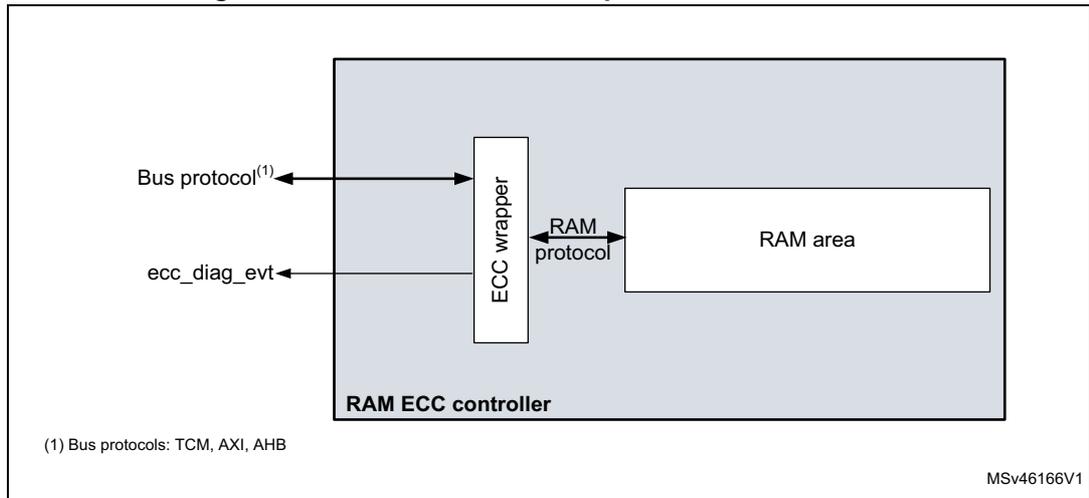
An ECC controller is associated to each RAM area. It performs the following functions:
- • ECC encoding: ECC code computation and storage.
- • ECC decoding: RAM data word loading and ECC code decoding to detect errors
- • Error detection: single- and double-error detection
- • Error correction: single-error correction.
Note: All the RAM ECC controllers are always enabled.
Figure 3 describes the implementation of RAM ECC controllers.
Figure 3. RAM ECC controller implementation schematic
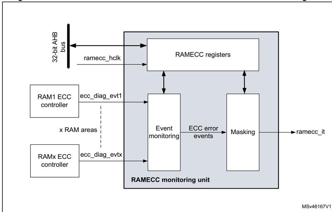
A dedicated RAM ECC monitoring area is defined for each domain (see Section 3.3.3: RAMECC monitor mapping ). The RAMECC allows the collection of ECC diagnostic events from each RAM ECC controller and provides a mean for the CPU to verify the ECC status.
Figure 4 shows the connection schematic between the RAM ECC controller and the RAMECC monitoring unit.
Figure 4. Connection between RAM ECC controller and RAMECC monitoring unit
3.3.2 RAMECC internal signals
Table 10 gives the list of the internal signals that control the RAMECC unit.
Table 10. RAMECC internal input/output signals
| Internal signal name | Signal type | Description |
|---|---|---|
| ramecc_hclk | Input | AHB clock |
| ecc_diag_evt | Input | ECC diagnostic event generated by RAMx ECC controller x |
| ramecc_it | Output | Interrupt generated by the RAMECC monitoring unit when an ECC error is detected. |
3.3.3 RAMECC monitor mapping
STM32H742, STM32H743/753 and STM32H750 devices features three RAMECC monitoring units (one per domain). The inputs from the ECC controllers are mapped as described in Table 11. The RAM ECC event monitoring status and configuration registers are described in Section 3.4: RAMECC registers .
Table 11. ECC controller mapping
| RAMECC units | Monitor number | SRAM ECC event monitoring status and configuration registers | Size in Kbytes | Address Offset | |
|---|---|---|---|---|---|
| D1 domain RAMECC unit | 1 | AXI SRAM ECC monitoring unit | 512 | 0x20 | |
| 2 | ITCM-RAM ECC monitoring unit | 64 | 0x40 | ||
| 3 | DTCM-RAM ECC monitoring unit | D0TCM | 64 | 0x60 | |
| 4 | D1TCM | 64 | 0x80 | ||
| 5 | ETM RAM ECC monitoring unit | 4 | 0xA0 | ||
| D2 domain RAMECC unit | 1 | SRAM1 ECC monitoring unit | SRAM1_0 | 64 | 0x20 |
| 2 | SRAM1_1 | 64 | 0x40 | ||
| 3 | SRAM2 ECC monitoring unit | SRAM2_0 | 64 | 0x60 | |
| 4 | SRAM2_1 | 64 | 0x80 | ||
| 5 | SRAM3 ECC monitoring unit | 32 | 0xA0 | ||
| D3 domain RAMECC unit | 1 | SRAM4 ECC monitoring unit | 64 | 0x20 | |
| 2 | Backup RAM ECC monitoring unit | 4 | 0x40 | ||
3.4 RAMECC registers
RAMECC registers can be accessed only in 32-bit (word) mode. Byte and half-word formats are not allowed.
3.4.1 RAMECC interrupt enable register (RAMECC_IER)
Address offset: 0x00
Reset value: 0x0000 0000
| 31 | 30 | 29 | 28 | 27 | 26 | 25 | 24 | 23 | 22 | 21 | 20 | 19 | 18 | 17 | 16 |
|---|---|---|---|---|---|---|---|---|---|---|---|---|---|---|---|
| Res. | Res. | Res. | Res. | Res. | Res. | Res. | Res. | Res. | Res. | Res. | Res. | Res. | Res. | Res. | Res. |
| 15 | 14 | 13 | 12 | 11 | 10 | 9 | 8 | 7 | 6 | 5 | 4 | 3 | 2 | 1 | 0 |
| Res. | Res. | Res. | Res. | Res. | Res. | Res. | Res. | Res. | Res. | Res. | Res. | GECCDEBIE | GECCDEIE | GECCSEIE | GIE |
| r/w | r/w | r/w | r/w |
Bits 31:4 Reserved, must be kept at reset value.
Bit 3 GECCDEBIE : Global ECC double error on byte write (BW) interrupt enable
When GECCDEBIE bit is set to 1, an interrupt is generated when an ECC double detection error occurs during a byte write operation to RAM (incomplete word write).
0: no interrupt generated when an ECC double detection error occurs on byte write
1: interrupt generated if an ECC double detection error occurs on byte write
Bit 2 GECCDEIE : Global ECC double error interrupt enable
When GECCDEIE bit is set to 1, an interrupt is generated when an ECC double detection error occurs during a read operation from RAM.
0: no interrupt generated when an ECC double detection error occurs
1: interrupt generated if an ECC double detection error occurs
Bit 1 GECCSEIE : Global ECC single error interrupt enable
When GECCSEIE bit is set to 1, an interrupt is generated when an ECC single error occurs during a read operation from RAM.
0: no interrupt generated when an ECC single error occurs
1: interrupt generated when an ECC single error occurs
Bit 0 GIE : Global interrupt enable
When GIE bit is set to 1, an interrupt is generated when an enabled global ECC error (GECCDEBIE, GECCDEIE or GECCSEIE) occurs.
0: no interrupt generated when an ECC error occurs
1: interrupt generated when an ECC error occurs
3.4.2 RAMECC monitor x configuration register (RAMECC_MxCR)
Address offset: 0x20 * x
Reset value: 0x0000 0000
x is the ECC monitoring unit number
| 31 | 30 | 29 | 28 | 27 | 26 | 25 | 24 | 23 | 22 | 21 | 20 | 19 | 18 | 17 | 16 |
|---|---|---|---|---|---|---|---|---|---|---|---|---|---|---|---|
| Res. | Res. | Res. | Res. | Res. | Res. | Res. | Res. | Res. | Res. | Res. | Res. | Res. | Res. | Res. | Res. |
| 15 | 14 | 13 | 12 | 11 | 10 | 9 | 8 | 7 | 6 | 5 | 4 | 3 | 2 | 1 | 0 |
| Res. | Res. | Res. | Res. | Res. | Res. | Res. | Res. | Res. | Res. | ECCLEN EN | ECCDE BWIE | ECCDE IE | ECCSE IE | Res. | Res. |
| rw | rw | rw | rw |
Bits 31:6 Reserved, must be kept at reset value.
Bit 5 ECCLEN : ECC error latching enable
When ECCLEN bit is set to 1, if an ECC error occurs (both for single error correction or double detection) during a read operation, the context (address, data and ECC code) that generated the error are latched to their respective registers.
0: no error context preserved when an ECC error occurs
1: error context preserved when an ECC error occurs
Bit 4 ECCDEBWIE : ECC double error on byte write (BW) interrupt enable
When ECCDEBWIE bit is set to 1, monitor x generates an interrupt when an ECC double detection error occurs during a byte write operation to RAM.
0: no interrupt generated when an ECC double detection error occurs on byte write
1: interrupt generated if an ECC double detection error occurs on byte write
Bit 3 ECCDEIE : ECC double error interrupt enable
When ECCDEIE bit is set to 1, monitor x generates an interrupt when an ECC double detection error occurs during a read operation from RAM.
0: no interrupt generated when an ECC double detection error occurs
1: interrupt generated if an ECC double detection error occurs
Bit 2 ECCSEIE : ECC single error interrupt enable
When ECCSEIE bit is set to 1, monitor x generates an interrupt when an ECC single error occurs during a read operation from RAM.
0: no interrupt generated when an ECC single error occurs
1: interrupt generated when an ECC single error occurs
Bits 1:0 Reserved, must be kept at reset value.
3.4.3 RAMECC monitor x status register (RAMECC_MxSR)
Address offset: 0x24 + 0x20 * (x - 1), (x= ECC monitoring unit number)
Reset value: 0x0000 0000
| 31 | 30 | 29 | 28 | 27 | 26 | 25 | 24 | 23 | 22 | 21 | 20 | 19 | 18 | 17 | 16 |
|---|---|---|---|---|---|---|---|---|---|---|---|---|---|---|---|
| Res. | Res. | Res. | Res. | Res. | Res. | Res. | Res. | Res. | Res. | Res. | Res. | Res. | Res. | Res. | Res. |
| 15 | 14 | 13 | 12 | 11 | 10 | 9 | 8 | 7 | 6 | 5 | 4 | 3 | 2 | 1 | 0 |
| Res. | Res. | Res. | Res. | Res. | Res. | Res. | Res. | Res. | Res. | Res. | Res. | Res. | DEBW DF | DEDF | SEDCF |
| rc_w0 | rc_w0 | rc_w0 |
Bits 31: 3 Reserved, must be kept at reset value.
Bit 2 DEBWDF : ECC double error on byte write (BW) detected flag
This bit is set by hardware. It is cleared by software by writing a 0
0: no error detected
1: error detected
Bit 1 DEDF : ECC double error detected flag
This bit is set by hardware. It is cleared by software by writing a 0
0: no error detected
1: error detected
Bit 0 SEDCF : ECC single error detected and corrected flag
This bit is set by hardware. It is cleared by software by writing a 0
0: no error detected and corrected
1: error detected and corrected
3.4.4 RAMECC monitor x failing address register (RAMECC_MxFAR)
Address offset: 0x28 + 0x20 * (x-1), (x= ECC monitoring unit number)
Reset value: 0x0000 0000
| 31 | 30 | 29 | 28 | 27 | 26 | 25 | 24 | 23 | 22 | 21 | 20 | 19 | 18 | 17 | 16 |
|---|---|---|---|---|---|---|---|---|---|---|---|---|---|---|---|
| FADD[31:16] | |||||||||||||||
| r | r | r | r | r | r | r | r | r | r | r | r | r | r | r | r |
| 15 | 14 | 13 | 12 | 11 | 10 | 9 | 8 | 7 | 6 | 5 | 4 | 3 | 2 | 1 | 0 |
| FADD[15:0] | |||||||||||||||
| r | r | r | r | r | r | r | r | r | r | r | r | r | r | r | r |
Bits 31:0 FADD[31:0] : ECC error failing address
When an ECC error occurs the FADD bitfield contains the address that generated the ECC error.
3.4.5 RAMECC monitor x failing data low register (RAMECC_MxFDRL)
Address offset: 0x2C + 0x20 * (x-1), (x= ECC monitoring unit number)
Reset value: 0x0000 0000
| 31 | 30 | 29 | 28 | 27 | 26 | 25 | 24 | 23 | 22 | 21 | 20 | 19 | 18 | 17 | 16 |
| FDATAL[31:16] | |||||||||||||||
| r | r | r | r | r | r | r | r | r | r | r | r | r | r | r | r |
| 15 | 14 | 13 | 12 | 11 | 10 | 9 | 8 | 7 | 6 | 5 | 4 | 3 | 2 | 1 | 0 |
| FDATAL[15:0] | |||||||||||||||
| r | r | r | r | r | r | r | r | r | r | r | r | r | r | r | r |
Bits 31:0 FDATAL[31:0] : Failing data low
When an ECC error occurs the FDATAL bitfield contains the LSB part of the data that generated the error. For 32-bit word SRAM, this bitfield contains the full memory word that generated the error.
3.4.6 RAMECC monitor x failing data high register (RAMECC_MxFDRH)
Address offset: 0x30 + 0x20 * (x-1), (x= ECC monitoring unit number)
Reset value: 0x0000 0000
| 31 | 30 | 29 | 28 | 27 | 26 | 25 | 24 | 23 | 22 | 21 | 20 | 19 | 18 | 17 | 16 |
| FDATAH[31:16] | |||||||||||||||
| r | r | r | r | r | r | r | r | r | r | r | r | r | r | r | r |
| 15 | 14 | 13 | 12 | 11 | 10 | 9 | 8 | 7 | 6 | 5 | 4 | 3 | 2 | 1 | 0 |
| FDATAH[15:0] | |||||||||||||||
| r | r | r | r | r | r | r | r | r | r | r | r | r | r | r | r |
Bits 31:0 FDATAH[31:0] : Failing data high (64-bit memory)
When an ECC error occurs the FDATAH bitfield contains the MSB part of the data that generated the error.
Note: This register is reserved in case of 32-bit word SRAM.
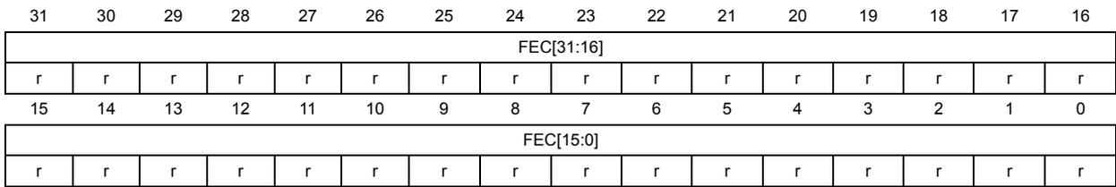
3.4.7 RAMECC monitor x failing ECC error code register (RAMECC_MxFECR)
Address offset: 0x34 + 0x20 * (x-1), (x= ECC monitoring unit number)
Reset value: 0x0000 0000
| 31 | 30 | 29 | 28 | 27 | 26 | 25 | 24 | 23 | 22 | 21 | 20 | 19 | 18 | 17 | 16 |
| FEC[31:16] | |||||||||||||||
| r | r | r | r | r | r | r | r | r | r | r | r | r | r | r | r |
| 15 | 14 | 13 | 12 | 11 | 10 | 9 | 8 | 7 | 6 | 5 | 4 | 3 | 2 | 1 | 0 |
| FEC[15:0] | |||||||||||||||
| r | r | r | r | r | r | r | r | r | r | r | r | r | r | r | r |
Bits 31:0 FEC [31:0] : Failing error code
When an ECC error occurs the FEC bitfield contains the ECC failing code that generated the error.
3.4.8 RAMECC register map
Table 12. RAMECC register map and reset values
| Offset | Register name reset value | Register size | ||||||||||||||||||||||||||||||||
|---|---|---|---|---|---|---|---|---|---|---|---|---|---|---|---|---|---|---|---|---|---|---|---|---|---|---|---|---|---|---|---|---|---|---|
| 31 | 30 | 29 | 28 | 27 | 26 | 25 | 24 | 23 | 22 | 21 | 20 | 19 | 18 | 17 | 16 | 15 | 14 | 13 | 12 | 11 | 10 | 9 | 8 | 7 | 6 | 5 | 4 | 3 | 2 | 1 | 0 | |||
| 0x00 | RAMECC_IER | Res | Res | Res | Res | Res | Res | Res | Res | Res | Res | Res | Res | Res | Res | Res | Res | Res | Res | Res | Res | Res | Res | Res | Res | Res | Res | Res | Res | Res | GECCDEBIE GECCDEIE GECCSEIE | GECCDEIE | GIE | |
| Reset value | 0 | 0 | 0 | 0 | ||||||||||||||||||||||||||||||
| 0x20 * x (x = monitoring unit number) | RAMECC_MxCR | Res | Res | Res | Res | Res | Res | Res | Res | Res | Res | Res | Res | Res | Res | Res | Res | Res | Res | Res | Res | Res | Res | Res | Res | Res | Res | Res | Res | Res | ECCELEN ECCDEBIE ECCDEIE ECCSEIE | ECCDEIE | Res | |
| Reset value | 0 | 0 | 0 | 0 | ||||||||||||||||||||||||||||||
| 0x24+0x20 *(x -1) (x = monitoring unit number) | RAMECC_MxSR | Res | Res | Res | Res | Res | Res | Res | Res | Res | Res | Res | Res | Res | Res | Res | Res | Res | Res | Res | Res | Res | Res | Res | Res | Res | Res | Res | Res | Res | Res | DEBWD DEDF | DEDF | SEDCF |
| Reset value | 0 | 0 | 0 | |||||||||||||||||||||||||||||||
| 0x28+0x20 *(x -1) (x = monitoring unit number) | RAMECC_MxFAR | FADD[31:0] | ||||||||||||||||||||||||||||||||
| Reset value | 0 | 0 | 0 | 0 | 0 | 0 | 0 | 0 | 0 | 0 | 0 | 0 | 0 | 0 | 0 | 0 | 0 | 0 | 0 | 0 | 0 | 0 | 0 | 0 | 0 | 0 | 0 | 0 | 0 | 0 | 0 | 0 | ||
| 0x2C+0x20 *(x -1) (x = monitoring unit number) | RAMECC_MxFDRL | FDATAL[31:0] | ||||||||||||||||||||||||||||||||
| Reset value | 0 | 0 | 0 | 0 | 0 | 0 | 0 | 0 | 0 | 0 | 0 | 0 | 0 | 0 | 0 | 0 | 0 | 0 | 0 | 0 | 0 | 0 | 0 | 0 | 0 | 0 | 0 | 0 | 0 | 0 | 0 | 0 | ||
| 0x30+0x20 *(x -1) (x = monitoring unit number) | RAMECC_MxFDRH | FDATAH[31:0] | ||||||||||||||||||||||||||||||||
| Reset value | 0 | 0 | 0 | 0 | 0 | 0 | 0 | 0 | 0 | 0 | 0 | 0 | 0 | 0 | 0 | 0 | 0 | 0 | 0 | 0 | 0 | 0 | 0 | 0 | 0 | 0 | 0 | 0 | 0 | 0 | 0 | 0 | ||
| 0x34+0x20 *(x -1) (x = monitoring unit number) | RAMECC_MxFECR | FEC[31:0] | ||||||||||||||||||||||||||||||||
| Reset value | 0 | 0 | 0 | 0 | 0 | 0 | 0 | 0 | 0 | 0 | 0 | 0 | 0 | 0 | 0 | 0 | 0 | 0 | 0 | 0 | 0 | 0 | 0 | 0 | 0 | 0 | 0 | 0 | 0 | 0 | 0 | 0 | ||
Refer to Section 2.3 on page 129 for the register boundary addresses.