33. True random number generator (RNG) applied to STM32L4P5xx and STM32L4Q5xx only
33.1 Introduction
The RNG is a true random number generator that provides full entropy outputs to the application as 32-bit samples. It is composed of a live entropy source (analog) and an internal conditioning component.
The RNG is a NIST SP 800-90B compliant entropy source that can be used to construct a non-deterministic random bit generator (NDRBG).
The RNG true random number generator has been pre-certified NIST SP800-90B. It has also been tested using German BSI statistical tests of AIS-31 (T0 to T8).
33.2 RNG main features
- • The RNG delivers 32-bit true random numbers, produced by an analog entropy source conditioned by a NIST SP800-90B approved conditioning stage.
- • It can be used as entropy source to construct a non-deterministic random bit generator (NDRBG).
- • It produces four 32-bit random samples every 412 AHB clock cycles if \( f_{\text{AHB}} < 77 \text{ MHz} \) (256 RNG clock cycles otherwise).
- • It embeds start-up and NIST SP800-90B approved continuous health tests (repetition count and adaptive proportion tests), associated with specific error management
- • It can be disabled to reduce power consumption, or enabled with an automatic low power mode (default configuration).
- • It has an AMBA AHB slave peripheral, accessible through 32-bit word single accesses only (else an AHB bus error is generated, and the write accesses are ignored).
33.3 RNG functional description
33.3.1 RNG block diagram
Figure 248 shows the RNG block diagram.
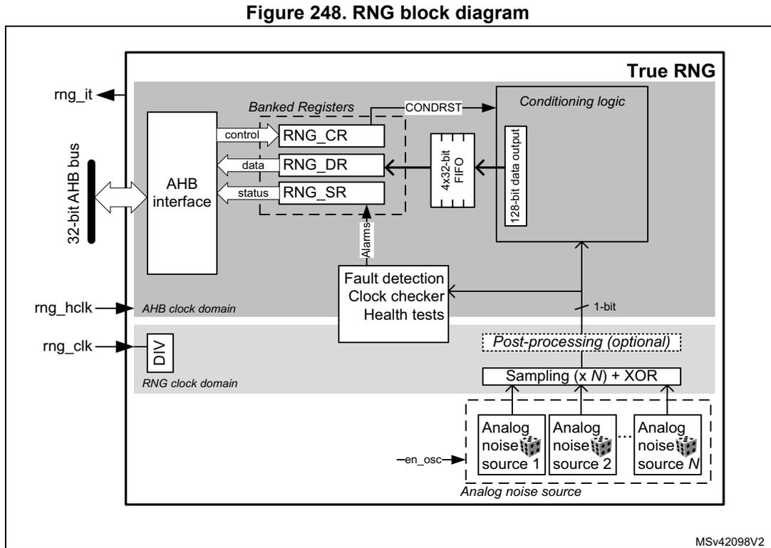
Figure 248. RNG block diagram
The diagram illustrates the internal architecture of the True RNG block. On the left, external signals are shown: rng_it (interrupt), rng_hclk (AHB clock), and rng_clk (dedicated clock). The rng_hclk connects to an AHB interface which is connected to a 32-bit AHB bus . The rng_clk passes through a DIV block into the RNG clock domain . Inside the True RNG block, the AHB interface connects to Banked Registers containing RNG_CR (control), RNG_DR (data), and RNG_SR (status). These registers connect to a 4x32-bit FIFO , which in turn connects to Conditioning logic and a 128-bit data output . A CONDRST signal is sent from the registers to the conditioning logic. Below the registers, a Fault detection block (containing Clock checker and Health tests ) receives Alarms from the registers and sends a 1-bit signal to the conditioning logic. In the RNG clock domain , there are multiple Analog noise source blocks (labeled Analog noise source 1 , Analog noise source 2 , ..., Analog noise source N ). These are connected to a Sampling (x N) + XOR block, which is part of an optional Post-processing stage. An -en_osc signal is also shown as an input to the noise sources. The diagram is labeled with MSv42098V2 at the bottom right.
33.3.2 RNG internal signals
Table 223 describes a list of useful-to-know internal signals available at the RNG level, not at the STM32 product level (on pads).
Table 223. RNG internal input/output signals
| Signal name | Signal type | Description |
|---|---|---|
| rng_it | Digital output | RNG global interrupt request |
| rng_hclk | Digital input | AHB clock |
| rng_clk | Digital input | RNG dedicated clock, asynchronous to rng_hclk |
33.3.3 Random number generation
The true random number generator (RNG) delivers truly random data through its AHB interface at deterministic intervals.
Within its boundary RNG integrates all the required NIST components depicted on Figure 249 . Those components are an analog noise source, a digitization stage, a conditioning algorithm, a health monitoring block and two interfaces that are used to interact with the entropy source: GetEntropy and HealthTest.
Figure 249. NIST SP800-90B entropy source model
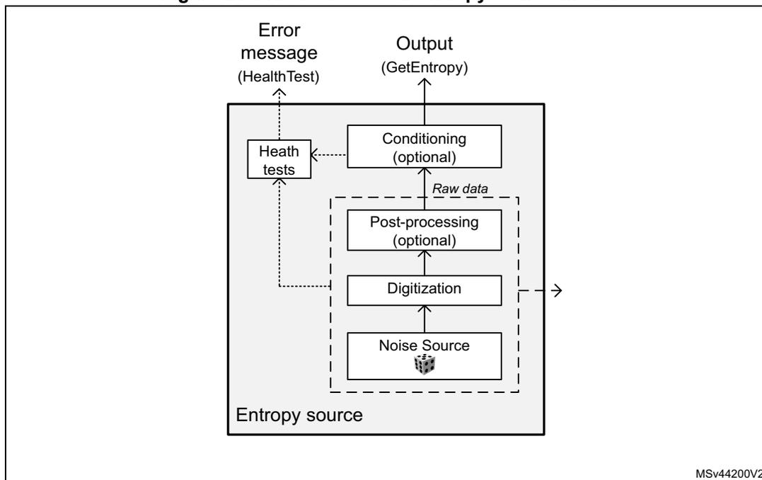
The components pictured above are detailed hereafter:
Noise source
The noise source is the component that contains the non-deterministic, entropy-providing activity that is ultimately responsible for the uncertainty associated with the bitstring output by the entropy source. This noise source provides 1-bit samples. It is composed of:
- • Multiple analog noise sources (x6), each based on three XORed free-running ring oscillator outputs. It is possible to disable those analog oscillators to save power, as described in Section 33.3.8: RNG low-power usage .
- • The XORing of the six noise sources into a single analog output.
- • A sampling stage of this output clocked by a dedicated clock input ( rng_clk with integrated divider), delivering a 1-bit raw data output.
This noise source sampling is independent to the AHB interface clock frequency ( rng_hclk ), with a possibility for the software to decrease the sampling frequency by using the integrated divider.
Note: In Section 33.6: RNG entropy source validation recommended RNG clock frequencies and associated divider value are given.
Post processing
In NIST configuration no post-processing is applied to sampled noise source. In non-NIST configuration B (as defined in Section 33.6.2 ) a normalization debiasing is applied, i.e. half of the bits are taken from the sampled noise source, half of the bits are taken from inverted sampled noise source.
Conditioning
The conditioning component in the RNG is a deterministic function that increases the entropy rate of the resulting fixed-length bitstrings output (128-bit). The NIST SP800-90B target is full entropy on the output (128-bit).
The times required between two random number generations, and between the RNG initialization and availability of first sample are described in Section 33.5: RNG processing time .
Output buffer
A data output buffer can store up to four 32-bit words that have been output from the conditioning component. When four words have been read from the output FIFO through the RNG_DR register, the content of the 128-bit conditioning output register is pushed into the output FIFO, and a new conditioning round is automatically started. Four new words are added to the conditioning output register after a number of clock cycles specified in Section 33.5: RNG processing time .
Whenever a random number is available through the RNG_DR register the DRDY flag transitions from 0 to 1. This flag remains high until output buffer becomes empty after reading four words from the RNG_DR register.
Note: When interrupts are enabled an interrupt is generated when this data ready flag transitions from 0 to 1. Interrupt is then cleared automatically by the RNG as explained above.
Health checks
This component ensures that the entire entropy source (with its noise source) starts then operates as expected, obtaining assurance that failures are caught quickly and with a high probability and reliability.
The RNG implements the following health check features in accordance with NIST SP800-90B. The described thresholds correspond to the value recommended for register RNG_HTCR (in Section 33.6.2 ).
- 1. Start-up health tests, performed after reset and before the first use of the RNG as entropy source
- – Adaptive proportion test running on one 1024 bit windows: the RNG verifies that the first bit on the outputs of the noise source is not repeated more than 628 times.
- – Known-answer tests, to verify the conditioning stage.
- – Repetition count test, flagging an error when the noise source has provided more than 40 consecutive bits at a constant value (0 or 1)
- 2. Continuous health tests, running indefinitely on the outputs of the noise source
- – Repetition count test, similar to the one running in start-up tests
- – Adaptive proportion test running on 1024 consecutive samples, like during start-up health tests.
- 3. Vendor specific continuous tests
- – Transition count test, flagging an error when the noise source has delivered more than 42 consecutive occurrence of two bits patterns (01 or 10).
- – Real-time “too slow” sampling clock detector, flagging an error when one RNG clock cycle (before divider) is smaller than AHB clock cycle divided by 32.
- 4. On-demand test of digitized noise source (raw data)
- – Supported by restarting the entropy source and re-running the startup tests (see software reset sequence in Section 33.3.4: RNG initialization ). Other kinds of on-demand testing (software based) are not supported .
The CECS and SECS status bits in the RNG_SR register indicate when an error condition is detected, as detailed in Section 33.3.7: Error management .
Note: An interrupt can be generated when an error is detected.
Above health test thresholds are modified by changing value in RNG_HTCR register. See Section 33.6: RNG entropy source validation for details.
33.3.4 RNG initialization
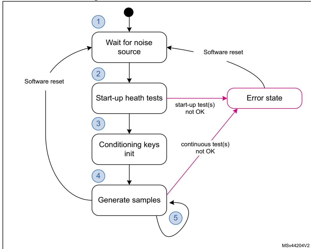
The RNG simplified state machine is pictured on Figure 250
After enabling the RNG (RNGEN = 1 in RNG_CR) the following chain of events occurs:
- 1. The analog noise source is enabled, and by default the RNG waits 16 cycles of RNG clock cycles (before divider) before starting to sample analog output and filling 128-bit conditioning shift register.
- 2. The conditioning hardware initializes, automatically triggering start-up behavior test on the raw data samples and known-answer tests.
- 3. When start-up health tests are completed. During this time three 128-bit noise source samples are used.
- 4. The conditioning stage internal input data buffer is filled again with 128-bit and a number of conditioning rounds defined by the RNG configuration (NIST or non-NIST) is performed. The output buffer is then filled with the post processing result.
- 5. The output buffer is refilled automatically according to the RNG usage.
The associated initialization time can be found in Section 33.5: RNG processing time .
Figure 250. RNG initialization overview
stateDiagram-v2
    [*] --> 1: Wait for noise source
    1 --> 2: Start-up health tests
    2 --> 3: Conditioning keys init
    3 --> 4: Generate samples
    4 --> 5: Generate samples (self-loop)
    2 --> Error state: start-up test(s) not OK
    4 --> Error state: continuous test(s) not OK
    Error state --> 1: Software reset
    Error state --> 4: Software reset
The diagram illustrates the RNG initialization state machine. It begins with an initial state (black dot) leading to state 1, 'Wait for noise source'. State 1 transitions to state 2, 'Start-up health tests'. State 2 transitions to state 3, 'Conditioning keys init'. State 3 transitions to state 4, 'Generate samples'. State 4 has a self-loop labeled 5, indicating continuous operation. State 2 can transition to an 'Error state' if 'start-up test(s) not OK'. State 4 can transition to an 'Error state' if 'continuous test(s) not OK'. From the 'Error state', a 'Software reset' can return the system to state 1 or state 4.
Figure 250 also highlights a possible software reset sequence, implemented by:
- Writing bits RNGEN = 0 and CONDRST = 1 in the RNG_CR register with the same RNG configuration and a new CLKDIV if needed.
- Then writing RNGEN = 1 and CONDRST = 0 in the RNG_CR register.
- Wait for random number to be ready, after initialization completes
Note: When RNG peripheral is reset through RCC (hardware reset) the RNG configuration for optimal randomness is lost in RNG registers. Software reset with CONFIGLOCK set preserves the RNG configuration.
33.3.5 RNG operation
Normal operations
To run the RNG using interrupts the following steps are recommended:
- Consult the
Section 33.6: RNG entropy source validation on page 1088
and verify if a specific RNG configuration is required for your application.
- If it is the case, write in the RNG_CR register the bit CONDRST = 1 together with the correct RNG configuration. Then perform a second write to the RNG_CR register with the bit CONDRST = 0, the interrupt enable bit IE = 1 and the RNG enable bit RNGEN = 1.
- If it is not the case perform a write to the RNG_CR register with the interrupt enable bit IE = 1 and the RNG enable bit RNGEN = 1.
- An interrupt is now generated when a random number is ready or when an error occurs. Therefore at each interrupt, check that:
- No error occurred. The SEIS and CEIS bits must be set to 0 in the RNG_SR register.
- A random number is ready. The DRDY bit must be set to 1 in the RNG_SR register.
- If above two conditions are true the content of the RNG_DR register can be read up to four consecutive times. If valid data is available in the conditioning output buffer, four additional words can be read by the application (in this case the DRDY bit is still high). If one or both of above conditions are false, the RNG_DR register must not be read. If an error occurred error recovery sequence described in Section 33.3.7 must be used.
To run the RNG in polling mode following steps are recommended:
- Consult the
Section 33.6: RNG entropy source validation on page 1088
and verify if a specific RNG configuration is required for your application.
- If it is the case write in the RNG_CR register the bit CONDRST = 1 together with the correct RNG configuration. Then perform a second write to the RNG_CR register with the bit CONDRST = 0 and the RNG enable bit RNGEN = 1.
- If it is not the case only enable the RNG by setting the RNGEN bit to 1 in the RNG_CR register.
- Read the RNG_SR register and check that:
- No error occurred (the SEIS and CEIS bits must be set to 0)
- A random number is ready (the DRDY bit must be set to 1)
- If above conditions are true read the content of the RNG_DR register up to four consecutive times. If valid data is available in the conditioning output buffer four
additional words can be read by the application (in this case the DRDY bit is still high). If one or both of above conditions are false, the RNG_DR register must not be read. If an error occurred error recovery sequence described in Section 33.3.7 must be used.
Note: When data is not ready (DRDY = 0) RNG_DR returns zero. It is recommended to always verify that RNG_DR is different from zero. Because when it is the case a seed error occurred between RNG_SR polling and RND_DR output reading (rare event).
If the random number generation period is a concern to the application and if NIST compliance is not required it is possible to select a faster RNG configuration by using the RNG configuration “B”, described in Section 33.6: RNG entropy source validation . The gain in random number generation speed is summarized in Section 33.5: RNG processing time .
Low-power operations
If the power consumption is a concern to the application, low-power strategies can be used, as described in Section 33.3.8: RNG low-power usage .
Software post-processing
No specific software post-processing/conditioning is expected to meet the AIS-31 or NIST SP800-90B approvals.
Built-in health check functions are described in Section 33.3.3: Random number generation .
33.3.6 RNG clocking
The RNG runs on two different clocks: the AHB bus clock and a dedicated RNG clock.
The AHB clock is used to clock the AHB banked registers and conditioning component. The RNG clock, coupled with a programmable divider (see CLKDIV bitfield in the RNG_CR register) is used for noise source sampling. Recommended clock configurations are detailed in Section 33.6: RNG entropy source validation .
Note: When the CED bit in the RNG_CR register is set to 0, the RNG clock frequency before internal divider must be higher than AHB clock frequency divided by 32, otherwise the clock checker always flags a clock error (CECS = 1 in the RNG_SR register).
See Section 33.3.1: RNG block diagram for details (AHB and RNG clock domains).
33.3.7 Error management
In parallel to random number generation an health check block verifies the correct noise source behavior and the frequency of the RNG source clock as detailed in this section. Associated error state is also described.
Clock error detection
When the clock error detection is enabled (CED = 0) and if the RNG clock frequency is too low, the RNG sets to 1 both the CEIS and CECS bits to indicate that a clock error occurred. In this case, the application should check that the RNG clock is configured correctly (see Section 33.3.6: RNG clocking ) and then it must clear the CEIS bit interrupt flag. The CECS bit is automatically cleared when clocking condition is normal.
Note: The clock error has no impact on generated random numbers, i.e. application can still read RNG_DR register.
CEIS is set only when CECS is set to 1 by RNG.
Noise source error detection
When a noise source (or seed) error occurs, the RNG stops generating random numbers and sets to 1 both SEIS and SECS bits to indicate that a seed error occurred. If a value is available in the RNG_DR register, it must not be used as it may not have enough entropy.
The following sequence must be used to fully recover from a seed error:
- 1. Software reset by writing CONDRST at 1 and at 0 (see bitfield description for details).
- 2. wait for CONDRST to be cleared in the RNG_CR register, then confirm that SEIS is cleared in the RNG_SR register.
- 3. wait for SECS to be cleared by RNG. The random number generation is now back to normal.
33.3.8 RNG low-power usage
If power consumption is a concern, the RNG can be disabled as soon as the DRDY bit is set to 1 by setting the RNGEN bit to 0 in the RNG_CR register. As the post-processing logic and the output buffer remain operational while RNGEN = 0 following features are available to software:
- • If there are valid words in the output buffer four random numbers can still be read from the RNG_DR register.
- • If there are valid bits in the conditioning output internal register four additional random numbers can be still be read from the RNG_DR register. If it is not the case RNG must be re-enabled by the application until the expected new noise source bits threshold is reached (128-bit in NIST mode) and a complete conditioning round is done.
Four new random words are then available only if the expected number of conditioning round is reached (two if NISTC = 0). The overall time can be found in Section 33.5: RNG processing time on page 1088 .
When disabling the RNG the user deactivates all the analog seed generators, whose power consumption is given in the datasheet electrical characteristics section. The user also gates all the logic clocked by the RNG clock. Note that this strategy is adding latency before a random sample is available on the RNG_DR register, because of the RNG initialization time.
If the RNG block is disabled during initialization (i.e. well before the DRDY bit rises for the first time), the initialization sequence resumes from where it was stopped when RNGEN bit is set to 1, unless the application resets the conditioning logic using CONDRST bit in the RNG_CR register.
33.4 RNG interrupts
In the RNG an interrupt can be produced on the following events:
- • Data ready flag
- • Seed error, see Section 33.3.7: Error management
- • Clock error, see Section 33.3.7: Error management
Dedicated interrupt enable control bits are available as shown in Table 224 .
Table 224. RNG interrupt requests
| Interrupt acronym | Interrupt event | Event flag | Enable control bit | Interrupt clear method |
|---|---|---|---|---|
| RNG | Data ready flag | DRDY | IE | None (automatic) |
| Seed error flag | SEIS | IE | Write 0 to SEIS or write CONDRST to 1 then to 0 | |
| Clock error flag | CEIS | IE | Write 0 to CEIS |
The user can enable or disable the above interrupt sources individually by changing the mask bits or the general interrupt control bit IE in the RNG_CR register. The status of the individual interrupt sources can be read from the RNG_SR register.
Note: Interrupts are generated only when RNG is enabled.
33.5 RNG processing time
In NIST compliant configuration, the time between two sets of four 32-bit data is either:
- • 412 AHB cycles if \( f_{\text{AHB}} < f_{\text{threshold}} \) (conditioning stage is limiting), or
- • 256 RNG cycles \( f_{\text{AHB}} \geq f_{\text{threshold}} \) (noise source stage is limiting).
With \( f_{\text{threshold}} = 1.6 \times f_{\text{RNG}} \) , e.g. 77 MHz if \( f_{\text{RNG}} = 48 \) MHz.
Note: When CLKDIV is different from zero, \( f_{\text{RNG}} \) must take into account the internal divider ratio.
33.6 RNG entropy source validation
33.6.1 Introduction
In order to assess the amount of entropy available from the RNG, STMicroelectronics has tested the peripheral using German BSI AIS-31 statistical tests (T0 to T8), and NIST SP800-90B test suite. The results can be provided on demand or the customer can reproduce the tests.
33.6.2 Validation conditions
STMicroelectronics has tested the RNG true random number generator in the following conditions:
- • RNG clock \( \text{rng\_clk} = 48 \) MHz
- • RNG configurations described in Table 225 . Note that only configuration A can be certified NIST SP800-90B.
Table 225. RNG configurations
| RNG Config | RNG_CR bits | Nb loop (N) | RNG_HTCR register (1) | |||||
|---|---|---|---|---|---|---|---|---|
| NISTC bit | RNG_CONFIG1 [5:0] | CLKDIV [3:0] | RNG_CONFIG2 [2:0] | RNG_CONFIG3 [3:0] | CED bit | |||
| A | 0 | 0x0F | 0x0 | 0x0 | 0xD | 0 | 2 | 0x0000 AA74 |
| B | 1 | 0x18 | 0x0 | 0x0 | 0x0 | 0 | 2 | |
- 1. When writing this register magic number 0x17590ABC must be written immediately before the indicated value
33.6.3 Data collection
In order to run statistical tests it is required to collect samples from the entropy source at raw data level as well as at the output of the entropy source. For details on data collection and the running of statistical test suites refer to “STM32 microcontrollers random number generation validation using NIST statistical test suite” application note (AN4230) available from www.st.com .
Contact STMicroelectronics if above samples need to be retrieved for your product.
33.7 RNG registers
The RNG is associated with a control register, a data register and a status register.
33.7.1 RNG control register (RNG_CR)
Address offset: 0x000
Reset value: 0x0080 0000
| 31 | 30 | 29 | 28 | 27 | 26 | 25 | 24 | 23 | 22 | 21 | 20 | 19 | 18 | 17 | 16 |
|---|---|---|---|---|---|---|---|---|---|---|---|---|---|---|---|
| CONFI GLOCK | COND RST | Res. | Res. | Res. | Res. | RNG_CONFIG1[5:0] | CLKDIV[3:0] | ||||||||
| rs | rw | rw | rw | rw | rw | rw | rw | rw | rw | rw | rw | ||||
| 15 | 14 | 13 | 12 | 11 | 10 | 9 | 8 | 7 | 6 | 5 | 4 | 3 | 2 | 1 | 0 |
|---|---|---|---|---|---|---|---|---|---|---|---|---|---|---|---|
| RNG_CONFIG2[2:0] | NISTC | RNG_CONFIG3[3:0] | Res. | Res. | CED | Res. | IE | RNGEN | Res. | Res. | |||||
| rw | rw | rw | rw | rw | rw | rw | rw | rw | rw | rw | |||||
Bit 31
CONFIGLOCK
: RNG Config lock
0: Writes to the RNG_CR configuration bits [29:4] are allowed.
1: Writes to the RNG_CR configuration bits [29:4] are ignored until the next RNG reset.
This bitfield is set once: if this bit is set it can only be reset to 0 if RNG is reset.
Bit 30
CONDRST
: Conditioning soft reset
Write 1 and then write 0 to reset the conditioning logic, clear all the FIFOs and start a new RNG initialization process, with RNG_SR cleared. Registers RNG_CR and RNG_NSCR are not changed by CONDRST.
This bit must be set to 1 in the same access that set any configuration bits [29:4]. In other words, when CONDRST bit is set to 1 correct configuration in bits [29:4] must also be written.
When CONDRST is set to 0 by software its value goes to 0 when the reset process is done. It takes about 2 AHB clock cycles + 2 RNG clock cycles.
Bits 29:26 Reserved, must be kept at reset value.
Bits 25:20
RNG_CONFIG1[5:0]
: RNG configuration 1
Reserved to the RNG configuration (bitfield 1). Must be initialized using the recommended value documented in
Section 33.6: RNG entropy source validation
.
Writing any bit of RNG_CONFIG1 is taken into account only if CONDRST bit is set to 1 in the same access, while CONFIGLOCK remains at 0. Writing to this bit is ignored if CONFIGLOCK = 1.
Bits 19:16 CLKDIV[3:0] : Clock divider factor
This value used to configure an internal programmable divider (from 1 to 16) acting on the incoming RNG clock. These bits can be written only when the core is disabled (RNGEN = 0).
0x0: internal RNG clock after divider is similar to incoming RNG clock.
0x1: two RNG clock cycles per internal RNG clock.
...
0xF: \( 2^{15} \) RNG clock cycles per internal clock (for example, an incoming 48MHz RNG clock becomes a 1.5 kHz internal RNG clock)
Writing these bits is taken into account only if CONDRST bit is set to 1 in the same access, while CONFIGLOCK remains at 0. Writing to this bit is ignored if CONFIGLOCK = 1.
Bits 15:13 RNG_CONFIG2[2:0] : RNG configuration 2
Reserved to the RNG configuration (bitfield 2). Refer to RNG_CONFIG1 bitfield for details.
Bit 12 NISTC : Non NIST compliant
0: Hardware default values for NIST compliant RNG. In this configuration per 128-bit output two conditioning loops are performed and 256 bits of noise source are used.
1: Custom values for NIST compliant RNG. See Section 33.6: RNG entropy source validation for proposed configuration.
Writing this bit is taken into account only if CONDRST bit is set to 1 in the same access, while CONFIGLOCK remains at 0. Writing to this bit is ignored if CONFIGLOCK = 1.
Bits 11:8 RNG_CONFIG3[3:0] : RNG configuration 3
Reserved to the RNG configuration (bitfield 3). Refer to RNG_CONFIG1 bitfield for details.
If NISTC bit is cleared in this register RNG_CONFIG3 bitfield values are ignored by RNG.
Bit 7 Reserved, must be kept at reset value.
Bit 6 Reserved, must be kept at reset value.
Bit 5 CED : Clock error detection
0: Clock error detection is enable
1: Clock error detection is disable
The clock error detection cannot be enabled nor disabled on-the-fly when the RNG is enabled, i.e. to enable or disable CED the RNG must be disabled.
Writing this bit is taken into account only if CONDRST bit is set to 1 in the same access, while CONFIGLOCK remains at 0. Writing to this bit is ignored if CONFIGLOCK = 1.
Bit 4 Reserved, must be kept at reset value.
Bit 3 IE : Interrupt Enable
0: RNG Interrupt is disabled
1: RNG Interrupt is enabled. An interrupt is pending as soon as DRDY = 1, SEIS = 1 or CEIS = 1 in the RNG_SR register.
Bit 2 RNGEN : True random number generator enable
0: True random number generator is disabled. Analog noise sources are powered off and logic clocked by the RNG clock is gated.
1: True random number generator is enabled.
Bits 1:0 Reserved, must be kept at reset value.
33.7.2 RNG status register (RNG_SR)
Address offset: 0x004
Reset value: 0x0000 0000
| 31 | 30 | 29 | 28 | 27 | 26 | 25 | 24 | 23 | 22 | 21 | 20 | 19 | 18 | 17 | 16 |
|---|---|---|---|---|---|---|---|---|---|---|---|---|---|---|---|
| Res. | Res. | Res. | Res. | Res. | Res. | Res. | Res. | Res. | Res. | Res. | Res. | Res. | Res. | Res. | Res. |
| 15 | 14 | 13 | 12 | 11 | 10 | 9 | 8 | 7 | 6 | 5 | 4 | 3 | 2 | 1 | 0 |
| Res. | Res. | Res. | Res. | Res. | Res. | Res. | Res. | Res. | SEIS | CEIS | Res. | Res. | SECS | CECS | DRDY |
| rc_w0 | rc_w0 | r | r | r |
Bits 31:7 Reserved, must be kept at reset value.
Bit 6 SEIS : Seed error interrupt status
This bit is set at the same time as SECS. It is cleared by writing 0 (unless CONDRST is used). Writing 1 has no effect.
0: No faulty sequence detected
1: At least one faulty sequence is detected. See
SECS
bit description for details.
An interrupt is pending if IE = 1 in the RNG_CR register.
Bit 5 CEIS : Clock error interrupt status
This bit is set at the same time as CECS. It is cleared by writing 0. Writing 1 has no effect.
0: The RNG clock is correct (
\(
f_{\text{RNGCLK}} > f_{\text{HCLK}}/32
\)
)
1: The RNG clock before internal divider is detected too slow (
\(
f_{\text{RNGCLK}} < f_{\text{HCLK}}/32
\)
)
An interrupt is pending if IE = 1 in the RNG_CR register.
Bits 4:3 Reserved, must be kept at reset value.
Bit 2 SECS : Seed error current status
0: No faulty sequence has currently been detected. If the SEIS bit is set, this means that a faulty sequence was detected and the situation has been recovered.
1: At least one of the following faulty sequence has been detected:
- – Run-time repetition count test failed (noise source has provided more than 24 consecutive bits at a constant value 0 or 1, or more than 32 consecutive occurrence of two bits patterns 01 or 10)
- – Start-up or continuous adaptive proportion test on noise source failed.
- – Start-up post-processing/conditioning sanity check failed.
Bit 1 CECS : Clock error current status
0: The RNG clock is correct (
\(
f_{\text{RNGCLK}} > f_{\text{HCLK}}/32
\)
). If the CEIS bit is set, this means that a slow clock was detected and the situation has been recovered.
1: The RNG clock is too slow (
\(
f_{\text{RNGCLK}} < f_{\text{HCLK}}/32
\)
).
Note: CECS bit is valid only if the CED bit in the RNG_CR register is set to 0.
Bit 0 DRDY : Data Ready
0: The RNG_DR register is not yet valid, no random data is available.
1: The RNG_DR register contains valid random data.
Once the output buffer becomes empty (after reading the RNG_DR register), this bit returns to 0 until a new random value is generated.
Note: The DRDY bit can rise when the peripheral is disabled (RNGEN = 0 in the RNG_CR register).
If IE=1 in the RNG_CR register, an interrupt is generated when DRDY = 1.
33.7.3 RNG data register (RNG_DR)
Address offset: 0x008
Reset value: 0x0000 0000
The RNG_DR register is a read-only register that delivers a 32-bit random value when read. The content of this register is valid when DRDY = 1 and value is not 0x0, even if RNGEN = 0.
| 31 | 30 | 29 | 28 | 27 | 26 | 25 | 24 | 23 | 22 | 21 | 20 | 19 | 18 | 17 | 16 |
|---|---|---|---|---|---|---|---|---|---|---|---|---|---|---|---|
| RNDATA[31:16] | |||||||||||||||
| r | r | r | r | r | r | r | r | r | r | r | r | r | r | r | r |
| 15 | 14 | 13 | 12 | 11 | 10 | 9 | 8 | 7 | 6 | 5 | 4 | 3 | 2 | 1 | 0 |
| RNDATA[15:0] | |||||||||||||||
| r | r | r | r | r | r | r | r | r | r | r | r | r | r | r | r |
Bits 31:0 RNDATA[31:0] : Random data
32-bit random data which are valid when DRDY = 1. When DRDY = 0 RNDATA value is zero.
It is recommended to always verify that RNG_DR is different from zero. Because when it is the case a seed error occurred between RNG_SR polling and RND_DR output reading (rare event).
33.7.4 RNG health test control register (RNG_HTCR)
Address offset: 0x010
Reset value: 0x0000 5A4E
Writing in RNG_HTCR is taken into account only if CONDRST bit is set, and CONFIGLOCK bit is cleared in RNG_CR. Writing to this register is ignored if CONFIGLOCK=1.
| 31 | 30 | 29 | 28 | 27 | 26 | 25 | 24 | 23 | 22 | 21 | 20 | 19 | 18 | 17 | 16 |
|---|---|---|---|---|---|---|---|---|---|---|---|---|---|---|---|
| HTCFG[31:16] | |||||||||||||||
| rw | rw | rw | rw | rw | rw | rw | rw | rw | rw | rw | rw | rw | rw | rw | rw |
| 15 | 14 | 13 | 12 | 11 | 10 | 9 | 8 | 7 | 6 | 5 | 4 | 3 | 2 | 1 | 0 |
| HTCFG[15:0] | |||||||||||||||
| rw | rw | rw | rw | rw | rw | rw | rw | rw | rw | rw | rw | rw | rw | rw | rw |
Bits 31:0 HTCFG[31:0] : health test configuration
This configuration is used by RNG to configure the health tests. See Section 33.6: RNG entropy source validation for the recommended value.
Note: The RNG behavior, including the read to this register, is not guaranteed if a different value from the recommended value is written.
When reading or writing this register magic number; 0x17590ABC must be written immediately before to RNG_HTCR register.
33.7.5 RNG register map
Table 226 gives the RNG register map and reset values.
Table 226. RNG register map and reset map
| Offset | Register name | 31 | 30 | 29 | 28 | 27 | 26 | 25 | 24 | 23 | 22 | 21 | 20 | 19 | 18 | 17 | 16 | 15 | 14 | 13 | 12 | 11 | 10 | 9 | 8 | 7 | 6 | 5 | 4 | 3 | 2 | 1 | 0 | |
|---|---|---|---|---|---|---|---|---|---|---|---|---|---|---|---|---|---|---|---|---|---|---|---|---|---|---|---|---|---|---|---|---|---|---|
| 0x000 | RNG_CR | CONFIGLOCK | CONDRST | Res. | Res. | Res. | RNG_CONFIG1 [5:0] | CLKDIV [3:0] | RNG_CONFIG2 [2:0] | NISTC | RNG_CONFIG3 [3:0] | Res. | CED | Res. | IE | RNGEN | Res. | Res. | ||||||||||||||||
| Reset value | 0 | 0 | 0 | 0 | 1 | 0 | 0 | 0 | 0 | 0 | 0 | 0 | 0 | 0 | 0 | 0 | 0 | 0 | 0 | 0 | 0 | 0 | 0 | 0 | ||||||||||
| 0x004 | RNG_SR | Res. | Res. | Res. | Res. | Res. | Res. | Res. | Res. | Res. | Res. | Res. | Res. | Res. | Res. | Res. | Res. | Res. | Res. | Res. | Res. | Res. | Res. | Res. | Res. | Res. | SEIS | CEIS | Res. | Res. | SECS | CECS | DRDY | |
| Reset value | 0 | 0 | 0 | 0 | 0 | |||||||||||||||||||||||||||||
| 0x008 | RNG_DR | RNDATA[31:0] | ||||||||||||||||||||||||||||||||
| Reset value | 0 | 0 | 0 | 0 | 0 | 0 | 0 | 0 | 0 | 0 | 0 | 0 | 0 | 0 | 0 | 0 | 0 | 0 | 0 | 0 | 0 | 0 | 0 | 0 | 0 | 0 | 0 | 0 | 0 | 0 | 0 | 0 | ||
| 0x010 | RNG_HTCR | HTCFG[31:0] | ||||||||||||||||||||||||||||||||
| Reset value | 0 | 0 | 0 | 0 | 0 | 0 | 0 | 0 | 0 | 0 | 0 | 0 | 1 | 1 | 0 | 0 | 0 | 1 | 0 | 1 | 1 | 0 | 1 | 0 | 0 | 1 | 0 | 0 | 1 | 1 | 1 | 0 | ||
Refer to Section 2.2 on page 93 for the register boundary addresses.