20. OCTOSPI I/O manager (OCTOSPIM)
20.1 Introduction
The OCTOSPI I/O manager is a low-level interface that enables an efficient OCTOSPI pin assignment with a full I/O matrix (before alternate function map) and multiplex of single/dual/quad/octal SPI interfaces over the same bus.
20.2 OCTOSPIM main features
- • Supports up to two single/dual/quad/octal SPI interfaces
- • Supports up to two ports for pin assignment
- • Fully programmable I/O matrix for pin assignment by function (data/control/clock)
20.3 OCTOSPIM implementation
The table below describes the OCTOSPIM implementation on STM32L4+ Series devices. The full list of features is implemented in STM32L4P5xx and STM32L4Q5xx devices, while STM32L4Rxxx and STM32L4Sxxx devices support a reduced set of features.
Table 124. OCTOSPIM implementation on STM32L4+ Series
| OCTOSPI feature | STM32L4P5xx and STM32L4Q5xx | STM32L4Rxxx and STM32L4Sxxx |
|---|---|---|
| Supports up to two single/dual/quad/octal SPI interfaces | X | X |
| Supports up to three ports for pin assignment | X | X |
| Fully programmable I/O matrix for pin assignment | X | X |
| Supports time-multiplexed mode | X | - |
20.4 OCTOSPIM functional description
20.4.1 OCTOSPIM block diagram
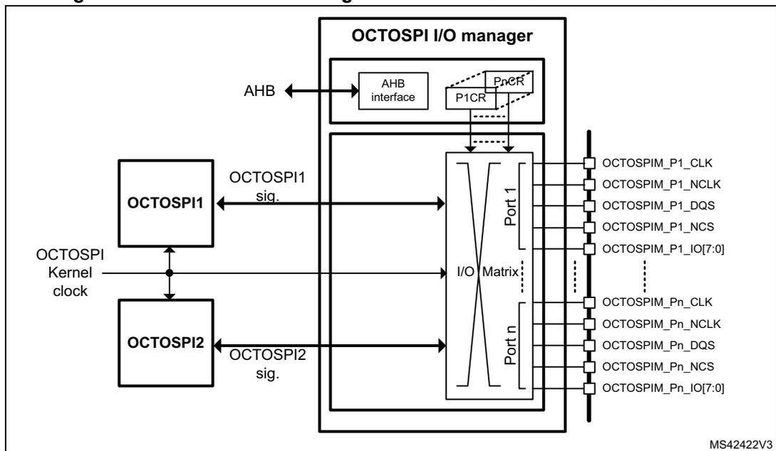
The block diagram of the OCTOSPI I/O manager is shown in Figure 85 .
Figure 85. OCTOSPIM block diagram for SMT32L4P5xx and STM32L4Q5xx
![Figure 85: OCTOSPIM block diagram for SMT32L4P5xx and STM32L4Q5xx. The diagram shows the internal architecture of the OCTOSPIM. At the top, an 'OCTOSPIM I/O manager' block contains an 'AHB interface', 'CR', and 'PnCR' registers. Below this, a 'MUXEN' block and a 'Muxer' block are shown. Two external blocks, 'OCTOSPI1' and 'OCTOSPI2', are connected to the 'Muxer'. 'OCTOSPI1' sends 'OCTOSPI1 signal', 'ACK1', and 'REQ1' signals. 'OCTOSPI2' sends 'REQ2', 'ACK2', and 'OCTOSPI2 signal' signals. The 'Muxer' outputs are connected to an 'I/O Matrix' block, which is divided into 'Port 1' and 'Port n'. The 'I/O Matrix' is connected to external pins: OCTOSPIM_P1_CLK, OCTOSPIM_P1_NCLK, OCTOSPIM_P1_DQS, OCTOSPIM_P1_NCS, OCTOSPIM_P1_IO[7:0], OCTOSPIM_Pn_CLK, OCTOSPIM_Pn_NCLK, OCTOSPIM_Pn_DQS, OCTOSPIM_Pn_NCS, and OCTOSPIM_Pn_IO[7:0]. The reference code MS42409V4 is in the bottom right corner.](/RM0432-STM32L4+/f755e322c481b280548bfe7e671ba780_img.jpg)
- 1. The number of ports (n) is 2.
- 2. Arbitration is possible for both I/O matrix input ports.
Figure 86. OCTOSPIM block diagram for SMT32L4Rxxx and STM32L4Sxxx
- 1. The number of ports (n) is 2.
20.4.2 OCTOSPIM matrix
The OCTOSPI I/O manager matrix allows the user to set a fully programmable pre-mapping of functions:
- • Any OCTOSPIM_Pn_CLK / OCTOSPIM_Pn_NCLK pair can be mapped independently to OCTOSPI1_CLK/OCTOSPI1_NCLK or OCTOSPI2_CLK/OCTOSPI2_NCLK
- • Any OCTOSPIM_Pn_DQS can be mapped independently to OCTOSPI1_DQS or OCTOSPI2_DQS
- • Any OCTOSPIM_Pn_NCS can be mapped independently to OCTOSPI1_NCS or OCTOSPI2_NCS
- • Any OCTOSPIM_Pn_IO[3:0] and OCTOSPIM_Pn_IO[7:4] can be mapped independently to OCTOSPI1_IO[3:0], OCTOSPI1_IO[7:4], OCTOSPI2_IO1[3:0] or OCTOSPI2_IO[7:4]
For each OCTOSPI I/O manager port, individual signal enables and mapping are configured through the corresponding OCTOSPI I/O manager Port n configuration register (OCTOSPIM_PnCR).
When several I/O pins have the same configuration, and are enabled at the same time, the result can be unpredictable.
In the default out-of-reset configuration, all the OCTOSPI1 or HSPI1 and OCTOSPI2 or HSPI2 signals are mapped, respectively, on Port 1 and on Port 2.
The OCTOSPIM configuration can be changed only when all OCTOSPIs or HSPIs are disabled.
20.4.3 OCTOSPIM multiplexed mode
When this mode is set the OCTOSPIs or HSPIs are time-multiplexed over the same bus. They get the ownership of the bus (in turn) through a request/acknowledge protocol with REQ/ACK signals.
The time-multiplexing is enabled by setting the MUXEN bit of the configuration register OCTOSPIM_CR.
The fairness counter (MAXTRAN) of each OCTOSPI or HSPI can be used to accurately manage the maximum duration for which a given OCTOSPI or HSPI takes the bus: this feature ensures a maximum bus access latency for the other OCTOSPI(s) or HSPI(s). When the bus is released by one OCTOSPI or HSPI, an arbitration phase occurs, which is round-robin: when another OCTOSPI or HSPI requests the bus, it gets it.
When the multiplexed mode is enabled, either the fairness counter or the refresh timeout counter of both OCTOSPI or HSPI interfaces must be activated.
OCTOSPI_nCS are not part of the multiplexing. Only OCTOSPI_n_IOs, OCTOSPI_n_DQS and OCTOSPI_n_CLK / OCTOSPI_n_NCLK are multiplexed.
When the multiplexed mode is used, only clock mode 0 is supported on the OCTOSPIs or HSPIs.
Due to arbitration and bus sharing, the auto polling interval time of the OCTOSPI or HSPI, when used, may be increased.
Minimum switching duration
The minimum number of cycles needed to switch from an OCTOSPI or HSPI to another can be configured.
This internal timer guarantees a latency between the falling edge of the REQ signal of the active OCTOSPI or HSPI (the active one releases the bus), and the rising edge of the ACK signal to the requesting OCTOSPI or HSPI (the bus is granted to the requesting one).
The duration is defined by the REQ2ACK_TIME field of the configuration register OCTOSPIM_CR.
Pin mapping in Multiplexed mode
In Multiplexed mode, the mapping of the bus is done as described below:
- • OCTOSPI1_nCS and OCTOSPI2_NCS work in the same way, then in Non-multiplexed mode they have to be assigned to their respective OCTOSPIM_Pn_NCS.
- • All the other signals are seen by the I/O matrix as if they were seen from OCTOSPI1.
20.5 OCTOSPIM registers
20.5.1 OCTOSPIM control register (OCTOSPIM_CR)
Address offset: 0x0000
Reset value: 0x0000 0000
| 31 | 30 | 29 | 28 | 27 | 26 | 25 | 24 | 23 | 22 | 21 | 20 | 19 | 18 | 17 | 16 |
|---|---|---|---|---|---|---|---|---|---|---|---|---|---|---|---|
| Res. | Res. | Res. | Res. | Res. | Res. | Res. | Res. | REQ2ACK_TIME[7:0] | |||||||
| rw | rw | rw | rw | rw | rw | rw | rw | ||||||||
| 15 | 14 | 13 | 12 | 11 | 10 | 9 | 8 | 7 | 6 | 5 | 4 | 3 | 2 | 1 | 0 |
| Res. | Res. | Res. | Res. | Res. | Res. | Res. | Res. | Res. | Res. | Res. | Res. | Res. | Res. | Res. | MUXEN |
| rw | |||||||||||||||
Bits 31:24 Reserved, must be kept at reset value.
Bits 23:16 REQ2ACK_TIME[7:0] : REQ to ACK time
In Multiplexed mode (MUXEN = 1), this field defines the time between two transactions.
The value is the number of OCTOSPI clock cycles - 1
Bits 15:1 Reserved, must be kept at reset value.
Bit 0 MUXEN : Multiplexed mode enable
This bit enables the multiplexing of the two OCTOSPIs.
0: No multiplexing, hence no arbitration
1: OCTOSPI1 and OCTOSPI2 are multiplexed over the same bus.
20.5.2 OCTOSPIM Port n configuration register (OCTOSPIM_PnCR)
Address offset: 0x0000 + 0x04*n (n=1 to 2)
Reset value: 0x0301 0111, 0x0705 0333
| 31 | 30 | 29 | 28 | 27 | 26 | 25 | 24 | 23 | 22 | 21 | 20 | 19 | 18 | 17 | 16 |
|---|---|---|---|---|---|---|---|---|---|---|---|---|---|---|---|
| Res. | Res. | Res. | Res. | Res. | IOHSRC[1:0] | IOHEN | Res. | Res. | Res. | Res. | Res. | IOLSRC[1:0] | IOLEN | ||
| rw | rw | rw | rw | rw | rw | ||||||||||
| 15 | 14 | 13 | 12 | 11 | 10 | 9 | 8 | 7 | 6 | 5 | 4 | 3 | 2 | 1 | 0 |
| Res. | Res. | Res. | Res. | Res. | Res. | NCSSRC | NCSEN | Res. | Res. | DQSSRC | DQSEN | Res. | Res. | CLKSRC | CLKEN |
| rw | rw | rw | rw | rw | rw | ||||||||||
Bits 31:27 Reserved, must be kept at reset value.
Bits 26:25 IOHSRC[1:0] : IO[7:4] source for Port n
This bits select the source of Port n IO[7:4].
00: OCTOSPI1_IO[3:0] in non multiplexed mode / multiplexed_IO[3:0] in multiplexed mode
01: OCTOSPI1_IO[7:4] in non multiplexed mode / multiplexed_IO[7:4] in multiplexed mode
10: OCTOSPI2_IO[3:0] in non multiplexed mode / unused in multiplexed mode
11: OCTOSPI2_IO[7:4] in non multiplexed mode / unused in multiplexed mode
Bit 24 IOHEN : IO[7:4] enable for Port n
This bit enables the Port n IO[7:4].
0: IO[7:4] for Port n disabled
1: IO[7:4] for Port n enabled
Bits 23:19 Reserved, must be kept at reset value.
Bits 18:17 IOLSRC[1:0] : IO[3:0] source for Port n
This bits select the source of Port n IO[3:0].
00: OCTOSPI1_IO[3:0] in non multiplexed mode / multiplexed_IO[3:0] in multiplexed mode
01: OCTOSPI1_IO[7:4] in non multiplexed mode / multiplexed_IO[7:4] in multiplexed mode
10: OCTOSPI2_IO[3:0] in non multiplexed mode / unused in multiplexed mode
11: OCTOSPI2_IO[7:4] in non multiplexed mode / unused in multiplexed mode
Bit 16 IOLEN : IO[3:0] enable for Port n
This bit enables the Port n IO[3:0].
0: IO[3:0] for Port n disabled
1: IO[3:0] for Port n enabled
Bits 15:10 Reserved, must be kept at reset value.
Bit 9 NCSSRC : nCS source for Port n
This bit selects the source of Port n nCS.
0: OCTOSPI1_nCS
1: OCTOSPI2_nCS
Bit 8 NCSEN : nCS enable for Port n
This bit enables the Port n nCS.
0: nCS for Port n is disabled
1: nCS for Port n is enabled
Bits 7:6 Reserved, must be kept at reset value.
Bit 5 DQSSRC : DQS source for Port n
This bit selects the source of Port n DQS.
0: OCTOSPI1_DQS in non multiplexed mode / multiplexed_DQS in multiplexed mode
1: OCTOSPI2_DQS in non multiplexed mode / unused port in multiplexed mode
Bit 4 DQSEN : DQS enable for Port n
This bit enables the Port n DQS.
0: DQS for Port n is disabled
1: DQS for Port n is enabled
Bits 3:2 Reserved, must be kept at reset value.
Bit 1 CLKSRC : CLK/CLKn source for Port n
This bit selects the source of Port n CLK/CLKn.
0: OCTOSPI1_CLK/CLKn in non multiplexed mode / multiplexed_CLK/CLKn in multiplexed mode
1: OCTOSPI2_CLK/CLKn in non multiplexed mode / unused port in multiplexed mode
Bit 0 CLKEN : CLK/CLKn enable for Port n
This bit enables the Port n CLK/CLKn.
0: CLK/CLKn for Port n is disabled
1: CLK/CLKn for Port n is enabled
20.5.3 OCTOSPIM register map
The following table summarizes the OCTOSPI I/O manager registers.
Table 125. OCTOSPIM register map and reset values
| Offset | Register name | 31 | 30 | 29 | 28 | 27 | 26 | 25 | 24 | 23 | 22 | 21 | 20 | 19 | 18 | 17 | 16 | 15 | 14 | 13 | 12 | 11 | 10 | 9 | 8 | 7 | 6 | 5 | 4 | 3 | 2 | 1 | 0 | |
|---|---|---|---|---|---|---|---|---|---|---|---|---|---|---|---|---|---|---|---|---|---|---|---|---|---|---|---|---|---|---|---|---|---|---|
| 0x0000 | OCTOSPIM_CR | Res. | Res. | Res. | Res. | Res. | Res. | Res. | Res. | REQ2ACK_TIME[7:0] | Res. | Res. | Res. | Res. | Res. | Res. | Res. | Res. | Res. | Res. | Res. | Res. | Res. | Res. | Res. | MUXEN | ||||||||
| Reset value | 0 | 0 | 0 | 0 | 0 | 0 | 0 | 0 | 0 | |||||||||||||||||||||||||
| 0x0004 | OCTOSPIM_P1CR | Res. | Res. | Res. | Res. | Res. | IOHSRC [1:0] | IOHEN | Res. | Res. | Res. | Res. | Res. | Res. | IOLSRC [1:0] | IOLEN | Res. | Res. | Res. | Res. | Res. | Res. | Res. | NCSSRC | NCSEN | Res. | Res. | Res. | DQSSRC | DQSEN | Res. | Res. | CLKSRC | CLKEN |
| Reset value | 0 | 1 | 1 | 0 | 0 | 1 | 0 | 1 | 0 | 1 | 0 | 1 | ||||||||||||||||||||||
| 0x0008 | OCTOSPIM_P2CR | Res. | Res. | Res. | Res. | Res. | IOHSRC [1:0] | IOHEN | Res. | Res. | Res. | Res. | Res. | Res. | IOLSRC [1:0] | IOLEN | Res. | Res. | Res. | Res. | Res. | Res. | Res. | NCSSRC | NCSEN | Res. | Res. | Res. | DQSSRC | DQSEN | Res. | Res. | CLKSRC | CLKEN |
| Reset value | 1 | 1 | 1 | 1 | 0 | 1 | 1 | 1 | 1 | 1 | 1 | 1 | ||||||||||||||||||||||
Refer to Section 2.2 on page 93 for the register boundary addresses.