14. Chrom-GRC (GFXMMU)
14.1 Introduction
The Chrom-GRC (GFXMMU) is a graphical oriented memory management unit aimed to optimize memory usage according to the display shape.
14.2 GFXMMU main features
- • Fully programmable display shape to physically store only the visible pixel
- • Up to 4 virtual buffers
- • Each virtual buffer have 3072 or 4096 bytes per line and 1024 lines
- • Each virtual buffer can be physically mapped to any system memory
- • Interrupt in case of buffer overflow (1 per buffer)
- • Interrupt in case of memory transfer error
14.3 GFXMMU functional and architectural description
The GFXMMU is responsible of address resolution to convert the virtual buffer address into the physical buffer address.
Figure 38. GFXMMU block diagram
![Figure 38. GFXMMU block diagram. The diagram shows the internal architecture of the GFXMMU. An input signal AHBSlaveAdd[23:0] enters the MMU block. The MMU outputs a physical address PhyAdd[22:0] and a partial address Add[23:22]. The Add[23:22] signal is used as an index for a multiplexer that selects between four virtual buffer addresses: pBuffer3AddMSB[31:23], pBuffer2AddMSB[31:23], pBuffer1AddMSB[31:23], and pBuffer0AddMSB[31:23]. The selected address is combined with the PhyAdd[22:0] to form the final output AHBMasterAdd[31:0]. To the right of the MMU are two blocks: 'Status registers' and 'Control registers'.](/RM0432-STM32L4+/dd8ee56b81790fa17fcc3c209c25bfef_img.jpg)
MSV41698V1
14.3.1 Virtual memory
The GFXMMU provides a virtual memory space seen by the system masters (a) . This virtual memory space is divided into four virtual buffers.
Virtual buffer
A virtual buffer is seen by any system master as a continuous memory space representing a virtual frame buffer of 1024 lines.
Each line is divided into 192 or 256 16-byte blocks depending on the 192BM bit of the GFXMMU configuration register (GFXMMU_CR).
Depending on the display shape and size, only the necessary blocks are mapped to a physical memory location. This mapping is done programming the LUT entry for each line:
- • The enable of the line
- • The number of the first “visible” block
- • The number of the last “visible” block
- • The address offset of the line within the physical buffer
The “visible” blocks can be arranged in the physical buffer in a continuous way programming the address offset of each line.
The LUT is common to all the buffers i.e. all the buffers have the same “shape”.
a. Refer to section “System architecture” for system masters accessing GFXMMU.
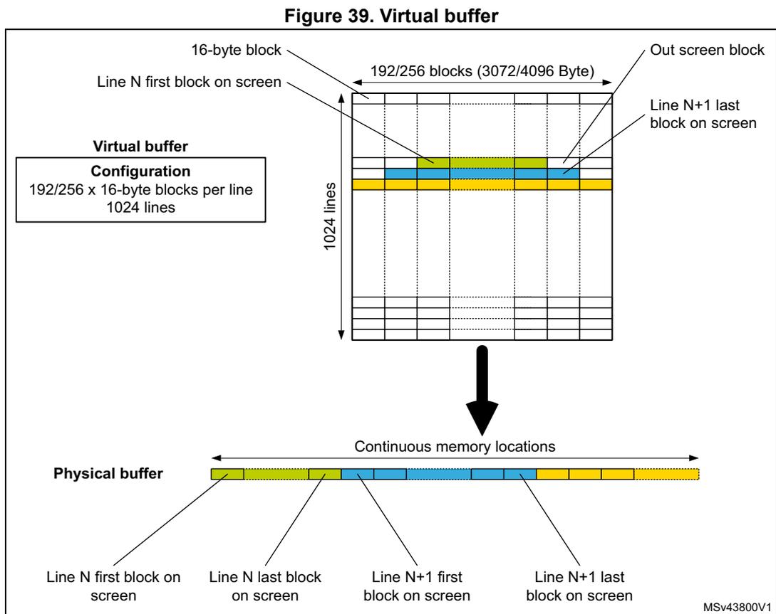
Figure 39. Virtual buffer
The diagram illustrates the mapping of a virtual buffer to a physical buffer. The virtual buffer is shown as a grid of 1024 lines and 192/256 blocks per line. The physical buffer is shown as a continuous memory location. Arrows indicate the mapping of specific blocks from the virtual buffer to the physical buffer.
Virtual buffer Configuration
192/256 x 16-byte blocks per line
1024 lines
Labels in the diagram:
- 16-byte block
- Line N first block on screen
- 192/256 blocks (3072/4096 Byte)
- Out screen block
- Line N+1 last block on screen
- 1024 lines
- Continuous memory locations
- Physical buffer
- Line N first block on screen
- Line N last block on screen
- Line N+1 first block on screen
- Line N+1 last block on screen
- MSV43800V1
Virtual buffer overview
For a frame buffer coded in 32 bpp or 16 bpp, the virtual buffer can be configured to have 192 or 256 blocks. This results in a virtual frame buffer of 768 x 1024 or 1024 x 1024 pixels for 32 bpp and 1536 x 1024 or 2048 x 1024 for 16 bpp.
For a frame buffer coded in 24 bpp, the virtual buffer must be configured to have 192 blocks to have an integer number of pixel per lines. This results in a virtual frame buffer of 1024 x 1024 pixels for 24 bpp.
Each buffer can be physically mapped anywhere in the physical memory thanks to:
- • The physical buffer base address (PBBA) field of the GFXMMU buffer x configuration register (GFXMMU_BxCR). It configures the physical location of the 8-Mbyte area where the buffer is mapped.
- • The physical buffer location respective to the physical buffer base address is defined by the physical buffer offset (PBO) field of the GFXMMU buffer x configuration register (GFXMMU_BxCR).
Figure 40. Virtual buffer and physical buffer memory map
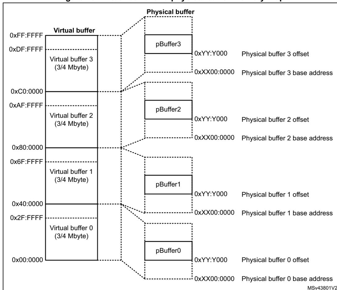
The diagram illustrates the memory mapping for four virtual buffers to four physical buffers. The virtual buffers are defined by their start and end addresses, each spanning 3/4 Mbyte. The physical buffers are shown with their base addresses and offsets. The mapping is as follows:
| Virtual buffer | Start Address | End Address | Physical buffer | Base Address | Offset |
|---|---|---|---|---|---|
| Virtual buffer 0 (3/4 Mbyte) | 0x00:0000 | 0x2F:FFFF | pBuffer0 | 0xXX00:0000 | 0xYY:Y000 |
| Virtual buffer 1 (3/4 Mbyte) | 0x40:0000 | 0x6F:FFFF | pBuffer1 | 0xXX00:0000 | 0xYY:Y000 |
| Virtual buffer 2 (3/4 Mbyte) | 0xAF:FFFF | 0xC0:0000 | pBuffer2 | 0xXX00:0000 | 0xYY:Y000 |
| Virtual buffer 3 (3/4 Mbyte) | 0xDF:FFFF | 0xFF:FFFF | pBuffer3 | 0xXX00:0000 | 0xYY:Y000 |
MSv43801V2
The buffer can not overflow the 8-Mbyte boundary of the zone defined by its base address. In case of overflow, the buffer x overflow flag (BxOF) of the GFXMMU status register (GFXMMU_SR) is set and an interrupt is generated if the buffer x overflow interrupt enable (BxOIE) bit of the GFXMMU configuration register (GFXMMU_CR) is set.
Virtual buffer application use case
As the physical locations are independently configurable, the four virtual buffers can be physically mapped to non continuous locations. This would allow for example to have the four buffers mapped on to four different SDRAM banks and avoid extra precharge cycles accessing the SDRAM.
As a consequence, one buffer must be used by the CPU/Chrom ART for frame buffer calculation while an other one must be used by the LTDC.
The two remaining buffers can be used as a graphical library requiring extra drawing buffers.
14.3.2 MMU architecture
The MMU block is responsible of the address resolution. It receives the 24-bit address and returns the physical 23-bit address and a valid signals to indicate the address is physically mapped or not. The MMU also checks overflow of a area boundary.
The MMU LUT is implemented as a 1024 x 35-bit RAM
Figure 41. MMU block diagram
![Figure 41. MMU block diagram. The diagram shows the internal architecture of the MMU. An input address Add[23:4] is split into three paths: a Line/block decoder, a LookUp RAM (1024 x 35-bit), and a pBufferOffset block. The Line/block decoder outputs Block[7:0] and Line[9:0]. The LookUp RAM outputs Block0Offset[21:4], LineEnable, FirstBlock[7:0], and LastBlock[7:0]. The pBufferOffset block outputs pBufferOffset[22:4]. Block0Offset[21:4] and pBufferOffset[22:4] are summed in an adder to produce a physical address. This address is compared with Line[9:0] in a comparator (C) to generate Overflow and PhyAdd[22:4] outputs. FirstBlock[7:0] and LastBlock[7:0] are compared in a Block valid comp. block to generate a Valid output.](/RM0432-STM32L4+/4a46791b788f496e351a2caa692c4a27_img.jpg)
Line block decoder
The line block decoder is generating the block number and the line number according the address.
Look up RAM
The look up RAM is a 1024 x 35-bit RAM with the following fields:
- • 1-bit line enable
- • 8-bit first valid block
- • 8-bit last valid block
- • 18-bit for line offset
As the RAM is bigger than a word, each entry is split into two words on the memory map. The write access are done in two steps:
- 1. Write the first word with enable/first valid block/last valid block in the GFXMMU_LUTxL memory location (internally buffered).
- 2. Write the second word with line offset in the GFXMMU_LUTxH memory location (effective write into the memory together with the internally buffered value).
A write in the LUT can happen any time but it can lead to inconsistencies if a master is using the MMU at the same time. As the CPU has the priority during LUT programming, this may slow down MMU calculation.
There is no restriction during read operations, but this may slow down CPU as the MMU has the priority on LUT accesses.
Block validation/comparator
This block is checking if the block is valid.
A block is considered as valid (physically mapped) when:
- • Line is enable.
- • The block number is greater or equal to the first valid block.
- • The block number is lower or equal to the last valid block.
When the block is valid, the physical address generated is considered as correct.
If the result of the MMU evaluation is not valid, the write operations are ignored, and read operations return the default 32-bit value stored in the default value (DV) field of the GFXMMU default value register (GFXMMU_DVR).
Block offset address calculation within the buffer
The block number is added to the line offset to get the offset of the block within the physical buffer.
As a consequence, the line offset stored in the LUT is given by the following formula:
with:
- • The maximum value for the line offset is when all the block of all the line are used. As the consequence the line offset for the last line can be maximum:
\( 1023 \times 256 \times 6 = 0x3F:F00x \) - • The minimum value for the line offset is when the last block of the first line is the first valid block: \( -255 \times 16 = -0xFFx \) i.e \( 0x3F:F01x \)
As the consequence the full range of the line offset entry of the LUT is used.
Carry is not taken into account as this stage to be able to perform negative offset calculations (values from \( 0x3F:F01x \) to \( 0x3F:FFFx \) )
As the block offset is within a 4-Mbyte buffer, the address generated is 22-bit wide.
Block offset address calculation
Once the offset of the block within the buffer has been calculated, this value is added to the offset of the block respective to the physical buffer base address.
The offset of the blocks are defined in registers as shown in Figure 42 :
Figure 42. Block validation/comparator implementation
![Diagram of Block validation/comparator implementation. It shows a block labeled 'PBufferOffset' containing four registers: pBuffer0Offset[22:4], pBuffer1Offset[22:4], pBuffer2Offset[22:4], and pBuffer3Offset[22:4]. An input 'Add[23:22]' is shown to the left. An arrow points from the 'PBufferOffset' block to an output labeled 'pBufferOffset[22:4]'. The diagram is labeled 'MSv43803V1' in the bottom right corner.](/RM0432-STM32L4+/c239160f286a6ea3596e64c82f29bfcd_img.jpg)
The resulting address and the buffer offset address must be on 23-bit.
The carry is taken into account to trigger address overflow. The carry is propagated to the GFXMMU status register (GFXMMU_SR) to set the buffer x overflow flag (BxOF).
Example of calculation
We are considering the following configuration for virtual buffer 0:
- • First visible block of line 0: block 7
- • Number of visible block in line 0: 10
- • First visible block of line 1: block 6
- • Number of visible block in line 1: 12
- • Address of the physical buffer: 0xC020:0000
The configuration must be:
- • The base address of the physical buffer 0: 0xC000:0000
- • The offset of buffer 0: 0x20:0000
- • First visible block of line 0: block 7
- • Last visible block of line 0: block 16
- • Block 0 offset of line 0: \( (0 - 7) \times 0x10 = -0x70 = 0x3F:FF90 \)
- • First visible block of line 1: block 6
- • Last visible block of line 1: block 17
- • Block 0 offset of line 1: \( (10 - 6) \times 0x10 = (0xA - 0x6) \times 0x10 = 0x40 \)
As a consequence:
- • the physical address of block 7 of line 0 is:
- • the physical address of block 16 of line 0 is:
- • the physical address of block 6 of line 1 is:
- • the physical address of block 17 of line 1 is:
14.4 GFXMMU interrupts
An interrupt can be produced on the following events:
- • Buffer 0 overflow
- • Buffer 1 overflow
- • Buffer 2 overflow
- • Buffer 3 overflow
- • AHB master error
Separate interrupt enable bits are available for flexibility.
Table 74. GFXMMU interrupt requests
| Interrupt event | Event flag | Enable control bit |
|---|---|---|
| Buffer 0 overflow | B0OF | B0OIE |
| Buffer 1 overflow | B1OF | B1OIE |
| Buffer 2 overflow | B2OF | B2OIE |
| Buffer 3 overflow | B3OF | B3OIE |
| AHB master error | AMEF | AMEIE |
14.5 GFXMMU registers
14.5.1 GFXMMU configuration register (GFXMMU_CR)
Address offset: 0x0000
Reset value: 0x0000 0000
| 31 | 30 | 29 | 28 | 27 | 26 | 25 | 24 | 23 | 22 | 21 | 20 | 19 | 18 | 17 | 16 |
|---|---|---|---|---|---|---|---|---|---|---|---|---|---|---|---|
| Res. | Res. | Res. | Res. | Res. | Res. | Res. | Res. | Res. | Res. | Res. | Res. | Res. | Res. | Res. | Res. |
| 15 | 14 | 13 | 12 | 11 | 10 | 9 | 8 | 7 | 6 | 5 | 4 | 3 | 2 | 1 | 0 |
| Res. | Res. | Res. | Res. | Res. | Res. | Res. | Res. | Res. | 192BM | Res. | AMEIE | B3OIE | B2OIE | B1OIE | B0OIE |
| rW | rW | rW | rW | rW | rW |
Bits 31:7 Reserved, must be kept at reset value.
Bit 6 192BM : 192 Block mode
This bit defines the number of blocks per line
0: 256 blocks per line
1: 192 blocks per line
Bit 5 Reserved, must be kept at reset value.
Bit 4 AMEIE : AHB master error interrupt enable
This bit enables the AHB master error interrupt.
0: Interrupt disable
1: Interrupt enabled
Bit 3 B3OIE : Buffer 3 overflow interrupt enable
This bit enables the buffer 3 overflow interrupt.
0: Interrupt disable
1: Interrupt enabled
Bit 2 B2OIE : Buffer 2 overflow interrupt enable
This bit enables the buffer 2 overflow interrupt.
0: Interrupt disable
1: Interrupt enabled
Bit 1 B1OIE : Buffer 1 overflow interrupt enable
This bit enables the buffer 1 overflow interrupt.
0: Interrupt disable
1: Interrupt enabled
Bit 0 B0OIE : Buffer 0 overflow interrupt enable
This bit enables the buffer 0 overflow interrupt.
0: Interrupt disable
1: Interrupt enabled
14.5.2 GFXMMU status register (GFXMMU_SR)
Address offset: 0x0004
Reset value: 0x0000 0000
| 31 | 30 | 29 | 28 | 27 | 26 | 25 | 24 | 23 | 22 | 21 | 20 | 19 | 18 | 17 | 16 |
|---|---|---|---|---|---|---|---|---|---|---|---|---|---|---|---|
| Res. | Res. | Res. | Res. | Res. | Res. | Res. | Res. | Res. | Res. | Res. | Res. | Res. | Res. | Res. | Res. |
| 15 | 14 | 13 | 12 | 11 | 10 | 9 | 8 | 7 | 6 | 5 | 4 | 3 | 2 | 1 | 0 |
| Res. | Res. | Res. | Res. | Res. | Res. | Res. | Res. | Res. | Res. | Res. | AMEF | B3OF | B2OF | B1OF | B0OF |
| r | r | r | r | r |
Bits 31:5 Reserved, must be kept at reset value.
Bit 4 AMEF : AHB master error flag
This bit is set when an AHB error happens during a transaction. It is cleared by writing 1 to CAMEF.
Bit 3 B3OF : Buffer 3 overflow flag
This bit is set when an overflow occurs during the offset calculation of the buffer 3. It is cleared by writing 1 to CB3OF.
Bit 2 B2OF : Buffer 2 overflow flag
This bit is set when an overflow occurs during the offset calculation of the buffer 2. It is cleared by writing 1 to CB2OF.
Bit 1 B1OF : Buffer 1 overflow flag
This bit is set when an overflow occurs during the offset calculation of the buffer 1. It is cleared by writing 1 to CB1OF.
Bit 0 B0OF : Buffer 0 overflow flag
This bit is set when an overflow occurs during the offset calculation of the buffer 0. It is cleared by writing 1 to CB0OF.
14.5.3 GFXMMU flag clear register (GFXMMU_FCR)
Address offset: 0x0008
Reset value: 0x0000 0000
| 31 | 30 | 29 | 28 | 27 | 26 | 25 | 24 | 23 | 22 | 21 | 20 | 19 | 18 | 17 | 16 |
|---|---|---|---|---|---|---|---|---|---|---|---|---|---|---|---|
| Res. | Res. | Res. | Res. | Res. | Res. | Res. | Res. | Res. | Res. | Res. | Res. | Res. | Res. | Res. | Res. |
| 15 | 14 | 13 | 12 | 11 | 10 | 9 | 8 | 7 | 6 | 5 | 4 | 3 | 2 | 1 | 0 |
| Res. | Res. | Res. | Res. | Res. | Res. | Res. | Res. | Res. | Res. | Res. | CAMEF | CB3OF | CB2OF | CB1OF | CB0OF |
| rc_w1 | rc_w1 | rc_w1 | rc_w1 | rc_w1 |
Bits 31:5 Reserved, must be kept at reset value.
Bit 4 CAMEF : Clear AHB master error flag
Writing 1 clears the AHB master error flag in the GFXMMU_SR register.
Bit 3 CB3OF : Clear buffer 3 overflow flag
Writing 1 clears the buffer 3 overflow flag in the GFXMMU_SR register.
Bit 2 CB2OF : Clear buffer 2 overflow flag
Writing 1 clears the buffer 2 overflow flag in the GFXMMU_SR register.
Bit 1 CB1OF : Clear buffer 1 overflow flag
Writing 1 clears the buffer 1 overflow flag in the GFXMMU_SR register.
Bit 0 CB0OF : Clear buffer 0 overflow flag
Writing 1 clears the buffer 0 overflow flag in the GFXMMU_SR register.
14.5.4 GFXMMU default value register (GFXMMU_DVR)
Address offset: 0x0010
Reset value: 0x0000 0000
| 31 | 30 | 29 | 28 | 27 | 26 | 25 | 24 | 23 | 22 | 21 | 20 | 19 | 18 | 17 | 16 |
| DV[31:16] | |||||||||||||||
| rw | rw | rw | rw | rw | rw | rw | rw | rw | rw | rw | rw | rw | rw | rw | rw |
| 15 | 14 | 13 | 12 | 11 | 10 | 9 | 8 | 7 | 6 | 5 | 4 | 3 | 2 | 1 | 0 |
| DV[15:0] | |||||||||||||||
| rw | rw | rw | rw | rw | rw | rw | rw | rw | rw | rw | rw | rw | rw | rw | rw |
Bits 31:0 DV[31:0] : Default value
This field indicates the default 32-bit value which is returned when a master accesses a virtual memory location not physically mapped.
14.5.5 GFXMMU buffer 0 configuration register (GFXMMU_B0CR)
Address offset: 0x0020
Reset value: 0x0000 0000
| 31 | 30 | 29 | 28 | 27 | 26 | 25 | 24 | 23 | 22 | 21 | 20 | 19 | 18 | 17 | 16 |
| PBBA[31:23] | PBO[22:16] | ||||||||||||||
| rw | rw | rw | rw | rw | rw | rw | rw | rw | rw | rw | rw | rw | rw | rw | rw |
| 15 | 14 | 13 | 12 | 11 | 10 | 9 | 8 | 7 | 6 | 5 | 4 | 3 | 2 | 1 | 0 |
| PBO[15:4] | Res. | Res. | Res. | Res. | |||||||||||
| rw | rw | rw | rw | rw | rw | rw | rw | rw | rw | rw | rw | ||||
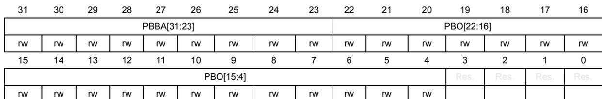
Bits 31:23 PBBA[31:23] : Physical buffer base address
Base address MSB of the physical buffer.
Bits 22:4 PBO[22:4] : Physical buffer offset
Offset of the physical buffer.
Bits 3:0 Reserved, must be kept at reset value.
14.5.6 GFXMMU buffer 1 configuration register (GFXMMU_B1CR)
Address offset: 0x0024
Reset value: 0x0000 0000
| 31 | 30 | 29 | 28 | 27 | 26 | 25 | 24 | 23 | 22 | 21 | 20 | 19 | 18 | 17 | 16 |
|---|---|---|---|---|---|---|---|---|---|---|---|---|---|---|---|
| PBBA[31:23] | PBO[22:16] | ||||||||||||||
| rw | rw | rw | rw | rw | rw | rw | rw | rw | rw | rw | rw | rw | rw | rw | rw |
| 15 | 14 | 13 | 12 | 11 | 10 | 9 | 8 | 7 | 6 | 5 | 4 | 3 | 2 | 1 | 0 |
| PBO[15:4] | Res. | Res. | Res. | Res. | |||||||||||
| rw | rw | rw | rw | rw | rw | rw | rw | rw | rw | rw | rw | ||||
Bits 31:23
PBBA[31:23]
: Physical buffer base address
Base address MSB of the physical buffer.
Bits 22:4
PBO[22:4]
: Physical buffer offset
Offset of the physical buffer.
Bits 3:0 Reserved, must be kept at reset value.
14.5.7 GFXMMU buffer 2 configuration register (GFXMMU_B2CR)
Address offset: 0x0028
Reset value: 0x0000 0000
| 31 | 30 | 29 | 28 | 27 | 26 | 25 | 24 | 23 | 22 | 21 | 20 | 19 | 18 | 17 | 16 |
|---|---|---|---|---|---|---|---|---|---|---|---|---|---|---|---|
| PBBA[31:23] | PBO[22:16] | ||||||||||||||
| rw | rw | rw | rw | rw | rw | rw | rw | rw | rw | rw | rw | rw | rw | rw | rw |
| 15 | 14 | 13 | 12 | 11 | 10 | 9 | 8 | 7 | 6 | 5 | 4 | 3 | 2 | 1 | 0 |
| PBO[15:4] | Res. | Res. | Res. | Res. | |||||||||||
| rw | rw | rw | rw | rw | rw | rw | rw | rw | rw | rw | rw | ||||
Bits 31:23
PBBA[31:23]
: Physical buffer base address
Base address MSB of the physical buffer.
Bits 22:4
PBO[22:4]
: Physical buffer offset
Offset of the physical buffer.
Bits 3:0 Reserved, must be kept at reset value.
14.5.8 GFXMMU buffer 3 configuration register (GFXMMU_B3CR)
Address offset: 0x002C
Reset value: 0x0000 0000
| 31 | 30 | 29 | 28 | 27 | 26 | 25 | 24 | 23 | 22 | 21 | 20 | 19 | 18 | 17 | 16 |
|---|---|---|---|---|---|---|---|---|---|---|---|---|---|---|---|
| PBBA[31:23] | PBO[22:16] | ||||||||||||||
| rw | rw | rw | rw | rw | rw | rw | rw | rw | rw | rw | rw | rw | rw | rw | rw |
| 15 | 14 | 13 | 12 | 11 | 10 | 9 | 8 | 7 | 6 | 5 | 4 | 3 | 2 | 1 | 0 |
| PBO[15:4] | Res. | Res. | Res. | Res. | |||||||||||
| rw | rw | rw | rw | rw | rw | rw | rw | rw | rw | rw | rw | ||||
Bits 31:23
PBBA[31:23]
: Physical buffer base address
Base address MSB of the physical buffer.
Bits 22:4
PBO[22:4]
: Physical buffer offset
Offset of the physical buffer.
Bits 3:0 Reserved, must be kept at reset value.
14.5.9 GFXMMU LUT entry x low (GFXMMU_LUTxL)
Address offset: 0x1000 + 8 * x, x = 0...1023
Reset value: 0x0000 0000
| 31 | 30 | 29 | 28 | 27 | 26 | 25 | 24 | 23 | 22 | 21 | 20 | 19 | 18 | 17 | 16 |
|---|---|---|---|---|---|---|---|---|---|---|---|---|---|---|---|
| Res. | Res. | Res. | Res. | Res. | Res. | Res. | Res. | LVB[7:0] | |||||||
| rw | rw | rw | rw | rw | rw | rw | rw | ||||||||
| 15 | 14 | 13 | 12 | 11 | 10 | 9 | 8 | 7 | 6 | 5 | 4 | 3 | 2 | 1 | 0 |
| FVB[7:0] | Res. | Res. | Res. | Res. | Res. | Res. | Res. | EN | |||||||
| rw | rw | rw | rw | rw | rw | rw | rw | rw | |||||||
Bits 31:24 Reserved, must be kept at reset value.
Bits 23:16
LVB[7:0]
: Last Valid Block
Number of the last valid block of line number X.
Bits 15:8
FVB[7:0]
: First Valid Block
Number of the first valid block of line number x.
Bits 7:1 Reserved, must be kept at reset value.
Bit 0
EN
: Enable
Line enable.
0: Line is disabled (no MMU evaluation is performed)
1: Line is enabled (MMU evaluation is performed)
14.5.10 GFXMMU LUT entry x high (GFXMMU_LUTxH)
Address offset: 0x1000 + 8 * x + 4, x = 0...1023
Reset value: 0x0000 0000
| 31 | 30 | 29 | 28 | 27 | 26 | 25 | 24 | 23 | 22 | 21 | 20 | 19 | 18 | 17 | 16 |
|---|---|---|---|---|---|---|---|---|---|---|---|---|---|---|---|
| Res. | Res. | Res. | Res. | Res. | Res. | Res. | Res. | Res. | Res. | LO[21:16] | |||||
| rw | rw | rw | rw | rw | rw | ||||||||||
| 15 | 14 | 13 | 12 | 11 | 10 | 9 | 8 | 7 | 6 | 5 | 4 | 3 | 2 | 1 | 0 |
|---|---|---|---|---|---|---|---|---|---|---|---|---|---|---|---|
| LO[15:4] | Res. | Res. | Res. | Res. | |||||||||||
| rw | rw | rw | rw | rw | rw | rw | rw | rw | rw | rw | rw | ||||
Bits 31:22 Reserved, must be kept at reset value.
Bits 21:4 LO[21:4] : Line offset
Line offset of line number x (i.e. offset of block 0 of line x)
Bits 3:0 Reserved, must be kept at reset value.
14.5.11 GFXMMU register map
The following table summarizes the graphic MMU registers. Refer to the register boundary addresses table for the graphic MMU register base address.
Table 75. GFXMMU register map and reset values
| Offset | Register | 31 | 30 | 29 | 28 | 27 | 26 | 25 | 24 | 23 | 22 | 21 | 20 | 19 | 18 | 17 | 16 | 15 | 14 | 13 | 12 | 11 | 10 | 9 | 8 | 7 | 6 | 5 | 4 | 3 | 2 | 1 | 0 |
|---|---|---|---|---|---|---|---|---|---|---|---|---|---|---|---|---|---|---|---|---|---|---|---|---|---|---|---|---|---|---|---|---|---|
| 0x0000 | GFXMMU_CR | Res. | Res. | Res. | Res. | Res. | Res. | Res. | Res. | Res. | Res. | Res. | Res. | Res. | Res. | Res. | Res. | Res. | Res. | Res. | Res. | Res. | Res. | Res. | Res. | Res. | 192BM | Res. | AMEIE | B30IE | B20IE | B10IE | B00IE |
| Reset value | 0 | 0 | 0 | 0 | 0 | ||||||||||||||||||||||||||||
| 0x0004 | GFXMMU_SR | Res. | Res. | Res. | Res. | Res. | Res. | Res. | Res. | Res. | Res. | Res. | Res. | Res. | Res. | Res. | Res. | Res. | Res. | Res. | Res. | Res. | Res. | Res. | Res. | Res. | Res. | Res. | AMEIF | B30F | B20F | B10F | B00F |
| Reset value | 0 | 0 | 0 | 0 | 0 | ||||||||||||||||||||||||||||
| 0x0008 | GFXMMU_FCR | Res. | Res. | Res. | Res. | Res. | Res. | Res. | Res. | Res. | Res. | Res. | Res. | Res. | Res. | Res. | Res. | Res. | Res. | Res. | Res. | Res. | Res. | Res. | Res. | Res. | Res. | CAMEF | CB30F | CB20F | CB10F | CB00F | |
| Reset value | 0 | 0 | 0 | 0 | 0 | ||||||||||||||||||||||||||||
| 0x000C | Reserved | Reserved | |||||||||||||||||||||||||||||||
| 0x0010 | GFXMMU_DVR | DV[31:0] | |||||||||||||||||||||||||||||||
| Reset value | 0 | 0 | 0 | 0 | 0 | 0 | 0 | 0 | 0 | 0 | 0 | 0 | 0 | 0 | 0 | 0 | 0 | 0 | 0 | 0 | 0 | 0 | 0 | 0 | 0 | 0 | 0 | 0 | 0 | 0 | 0 | 0 | |
| 0x0014-0x001C | Reserved | Reserved | |||||||||||||||||||||||||||||||
| 0x0020 | GFXMMU_B0CR | PBBA[31:23] | Res. | Res. | Res. | Res. | |||||||||||||||||||||||||||
| Reset value | 0 | 0 | 0 | 0 | 0 | 0 | 0 | 0 | 0 | 0 | 0 | 0 | 0 | 0 | 0 | 0 | 0 | 0 | 0 | 0 | 0 | 0 | 0 | 0 | 0 | 0 | 0 | 0 | |||||
| 0x0024 | GFXMMU_B1CR | PBBA[31:23] | Res. | Res. | Res. | Res. | |||||||||||||||||||||||||||
| Reset value | 0 | 0 | 0 | 0 | 0 | 0 | 0 | 0 | 0 | 0 | 0 | 0 | 0 | 0 | 0 | 0 | 0 | 0 | 0 | 0 | 0 | 0 | 0 | 0 | 0 | 0 | 0 | 0 | |||||
| 0x0028 | GFXMMU_B2CR | PBBA[31:23] | Res. | Res. | Res. | Res. | |||||||||||||||||||||||||||
| Reset value | 0 | 0 | 0 | 0 | 0 | 0 | 0 | 0 | 0 | 0 | 0 | 0 | 0 | 0 | 0 | 0 | 0 | 0 | 0 | 0 | 0 | 0 | 0 | 0 | 0 | 0 | 0 | 0 | |||||
| 0x002C | GFXMMU_B3CR | PBBA[31:23] | Res. | Res. | Res. | Res. | |||||||||||||||||||||||||||
| Reset value | 0 | 0 | 0 | 0 | 0 | 0 | 0 | 0 | 0 | 0 | 0 | 0 | 0 | 0 | 0 | 0 | 0 | 0 | 0 | 0 | 0 | 0 | 0 | 0 | 0 | 0 | 0 | 0 | |||||
| 0x0030-0x0FFC | Reserved | Reserved | |||||||||||||||||||||||||||||||
| 0x1000 | GFXMMU_LUT0L | Res. | Res. | Res. | Res. | Res. | Res. | Res. | Res. | LVB[7:0] | FVB[7:0] | Res. | Res. | Res. | Res. | Res. | Res. | Res. | EN | ||||||||||||||
| Reset value | 0 | 0 | 0 | 0 | 0 | 0 | 0 | 0 | 0 | 0 | 0 | 0 | 0 | 0 | 0 | 0 | 0 | ||||||||||||||||
| 0x1004 | GFXMMU_LUT0H | Res. | Res. | Res. | Res. | Res. | Res. | Res. | Res. | Res. | Res. | LO[21:4] | Res. | Res. | Res. | Res. | |||||||||||||||||
| Reset value | 0 | 0 | 0 | 0 | 0 | 0 | 0 | 0 | 0 | 0 | 0 | 0 | 0 | 0 | 0 | 0 | 0 | ||||||||||||||||
| ... | |||||||||||||||||||||||||||||||||
| 0x2FF8 | GFXMMU_LUT1023L | Res. | Res. | Res. | Res. | Res. | Res. | Res. | Res. | LVB[7:0] | FVB[7:0] | Res. | Res. | Res. | Res. | Res. | Res. | Res. | EN | ||||||||||||||
| Reset value | 0 | 0 | 0 | 0 | 0 | 0 | 0 | 0 | 0 | 0 | 0 | 0 | 0 | 0 | 0 | 0 | 0 | ||||||||||||||||
| 0x2FFC | GFXMMU_LUT1023H | Res. | Res. | Res. | Res. | Res. | Res. | Res. | Res. | Res. | Res. | LO[21:4] | Res. | Res. | Res. | Res. | |||||||||||||||||
| Reset value | 0 | 0 | 0 | 0 | 0 | 0 | 0 | 0 | 0 | 0 | 0 | 0 | 0 | 0 | 0 | 0 | 0 | ||||||||||||||||
Refer to Section 2.2 on page 93 for the register boundary addresses.