6. Reset and clock control (RCC)
6.1 Reset
There are three types of reset, defined as system reset, power reset and backup domain reset.
6.1.1 Power reset
A power reset is generated when one of the following events occurs:
- 1. a Brown-out reset (BOR).
- 2. when exiting from Standby mode.
- 3. when exiting from Shutdown mode.
A Brown-out reset, including power-on or power-down reset (POR/PDR), sets all registers to their reset values except the Backup domain.
When exiting Standby mode, all registers in the \( V_{CORE} \) domain are set to their reset value. Registers outside the \( V_{CORE} \) domain (RTC, WKUP, IWDG, and Standby/Shutdown modes control) are not impacted.
When exiting Shutdown mode, a Brown-out reset is generated, resetting all registers except those in the Backup domain.
6.1.2 System reset
A system reset sets all registers to their reset values except the reset flags in the clock control/status register (RCC_CSR) and the registers in the Backup domain.
A system reset is generated when one of the following events occurs:
- 1. A low level on the NRST pin (external reset)
- 2. Window watchdog event (WWDG reset)
- 3. Independent watchdog event (IWDG reset)
- 4. A firewall event (FIREWALL reset)
- 5. A software reset (SW reset) (see Software reset )
- 6. Low-power mode security reset (see Low-power mode security reset )
- 7. Option byte loader reset (see Option byte loader reset )
- 8. A Brown-out reset
The reset source can be identified by checking the reset flags in the Control/Status register, RCC_CSR (see Section 6.4.30: Control/status register (RCC_CSR) ).
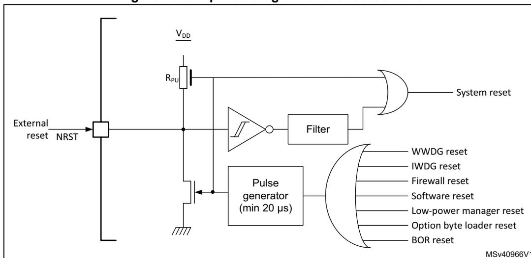
These sources act on the NRST pin and it is always kept low during the delay phase. The RESET service routine vector is fixed at address 0x0000_0004 in the memory map.
The system reset signal provided to the device is output on the NRST pin. The pulse generator guarantees a minimum reset pulse duration of 20 µs for each internal reset source. In case of an external reset, the reset pulse is generated while the NRST pin is asserted low.
In case of an internal reset, the internal pull-up \( R_{PU} \) is deactivated in order to save the power consumption through the pull-up resistor.
Figure 15. Simplified diagram of the reset circuit
Software reset
The SYSRESETREQ bit in Cortex ® -M4 Application Interrupt and Reset Control Register must be set to force a software reset on the device (refer to the STM32F3 , STM32F4 , STM32L4 and STM32L4+ Series Cortex ® -M4 (PM0214)).
Low-power mode security reset
To prevent that critical applications mistakenly enter a low-power mode, two low-power mode security resets are available. If enabled in option bytes, the resets are generated in the following conditions:
- 1. Entering Standby mode: this type of reset is enabled by resetting nRST_STDBY bit in User option Bytes. In this case, whenever a Standby mode entry sequence is successfully executed, the device is reset instead of entering Standby mode.
- 2. Entering Stop mode: this type of reset is enabled by resetting nRST_STOP bit in User option bytes. In this case, whenever a Stop mode entry sequence is successfully executed, the device is reset instead of entering Stop mode.
- 3. Entering Shutdown mode: this type of reset is enabled by resetting nRST_SHDW bit in User option bytes. In this case, whenever a Shutdown mode entry sequence is successfully executed, the device is reset instead of entering Shutdown mode.
For further information on the User Option Bytes, refer to Section 3.4.1: Option bytes description .
Option byte loader reset
The option byte loader reset is generated when the OBL_LAUNCH bit (bit 27) is set in the FLASH_CR register. This bit is used to launch the option byte loading by software.
6.1.3 Backup domain reset
The backup domain has two specific resets.
A backup domain reset is generated when one of the following events occurs:
- 1. Software reset, triggered by setting the BDRST bit in the Backup domain control register (RCC_BDCR) .
- 2. \( V_{DD} \) or \( V_{BAT} \) power on, if both supplies have previously been powered off.
A backup domain reset only affects the LSE oscillator, the RTC, the Backup registers and the RCC Backup domain control register.
6.2 Clocks
Four different clock sources can be used to drive the system clock (SYSCLK):
- • HSI16 (high speed internal) 16 MHz RC oscillator clock
- • MSI (multispeed internal) RC oscillator clock
- • HSE oscillator clock, from 4 to 48 MHz
- • PLL clock
The MSI is used as system clock source after startup from Reset, configured at 4 MHz.
The devices have the following additional clock sources:
- • 32 kHz low speed internal RC (LSI RC) which drives the independent watchdog and optionally the RTC used for Auto-wakeup from Stop and Standby modes.
- • 32.768 kHz low speed external crystal (LSE crystal) which optionally drives the real-time clock (RTCCLK).
- • RC 48 MHz internal clock sources (HSI48) to potentially drive the USB FS, the SDMMC and the RNG.
Each clock source can be switched on or off independently when it is not used, to optimize power consumption.
Several prescalers can be used to configure the AHB frequency, the APB1 and APB2 domains. The maximum frequency of the AHB, the APB1 and the APB2 domains is 120 MHz.
All the peripheral clocks are derived from their bus clock (HCLK, PCLK1 or PCLK2) except:
- • The 48 MHz clock, used for USB OTG FS, SDMMC and RNG. This clock is derived (selected by software) from one of the four following sources:
- – main PLL VCO (PLL48M1CLK)
- – PLLSAI1 VCO (PLL48M2CLK)
- – MSI clock
- – HSI48 internal oscillator
When the MSI clock is auto-trimmed with the LSE, it can be used by the USB OTG FS device.
When available, the HSI48 48 MHz clock can be coupled to the clock recovery system allowing adequate clock connection for the USB OTG FS (Crystal less solution).
- • The ADCs clock which is derived (selected by software) from one of the following sources:
- – system clock (SYSCLK)
- – PLLSAI1 VCO (PLLADC1CLK)
- • The U(S)ARTs clocks which are derived (selected by software) from one of the four following sources:
- – system clock (SYSCLK)
- – HSI16 clock
- – LSE clock
- – APB1 or APB2 clock (PCLK1 or PCLK2 depending on which APB is mapped the U(S)ART)
The wakeup from Stop mode is supported only when the clock is HSI16 or LSE.
- • The I
2
Cs clocks which are derived (selected by software) from one of the three following sources:
- – system clock (SYSCLK)
- – HSI16 clock
- – APB1 clock (PCLK1)
The wakeup from Stop mode is supported only when the clock is HSI16.
- • The SAI1 and SAI2 clocks which are derived (selected by software) from one of the following sources:
- – an external clock mapped on SAI1_EXTCLK for SAI1 and SAI2_EXTCLK for SAI2
- – PLLSAI1 VCO (PLLSAI1CLK)
- – PLLSAI2 VCO (PLLSAI2CLK)
- – main PLL VCO (PLLSAI3CLK)
- – HSI16 clock
- • The DFSDM audio clock which is derived (selected by software) from one of the following sources:
- – SAI1 clock
- – HSI clock
- – MSI clock
- • The LTDC clock. The LTDC clock is generated from a specific PLL (PLLSAI2).
- • The DSI clock. To generate the DSI clocks, the high-speed external crystal (HSE) must be available.
- – The DSI lanebyteclk clock: DSI Lane byte clock (high-speed clock divided by 8) which is output from the DSI-PHY or from a specific output of PLLSAI2 (frequency lower than 62.5 MHz) in the case when the DSI-PHY is off.
- – The DSI host rxclkesc clock. The DSI RX escape mode clock is output from DSI-PHY (generated from DP0/DN0 even if the DSI-PHY is not clocked).
- • The OctoSPI kernel clock which is derived (selected by software) from one of the following sources:
- – System clock,
- – PLL48M1CLK
- – MSI clock
- • The low-power timers (LPTIMx) clock which are derived (selected by software) from one of the five following sources:
- – LSI clock
- – LSE clock
- – HSI16 clock
- – APB1 clock (PCLK1)
- – External clock mapped on LPTIMx_IN1
The functionality in Stop mode (including wakeup) is supported only when the clock is LSI or LSE, or in external clock mode.
- • The RTC clock which is derived (selected by software) from one of the three following sources:
- – LSE clock
- – LSI clock
- – HSE clock divided by 32
The functionality in Stop mode (including wakeup) is supported only when the clock is LSI or LSE.
- • The IWDG clock which is always the LSI clock.
The RCC feeds the Cortex ® System Timer (SysTick) external clock with the AHB clock (HCLK) divided by 8. The SysTick can work either with this clock or directly with the Cortex ® clock (HCLK), configurable in the SysTick Control and Status Register.
FCLK acts as Cortex ® -M4 free-running clock. For more details refer to the STM32F3, STM32F4, STM32L4 and STM32L4+ Series Cortex ® -M4 programming manual (PM0214) .
Figure 16. Clock tree for STM32L4Rxxx and STM32L4Sxxx devices
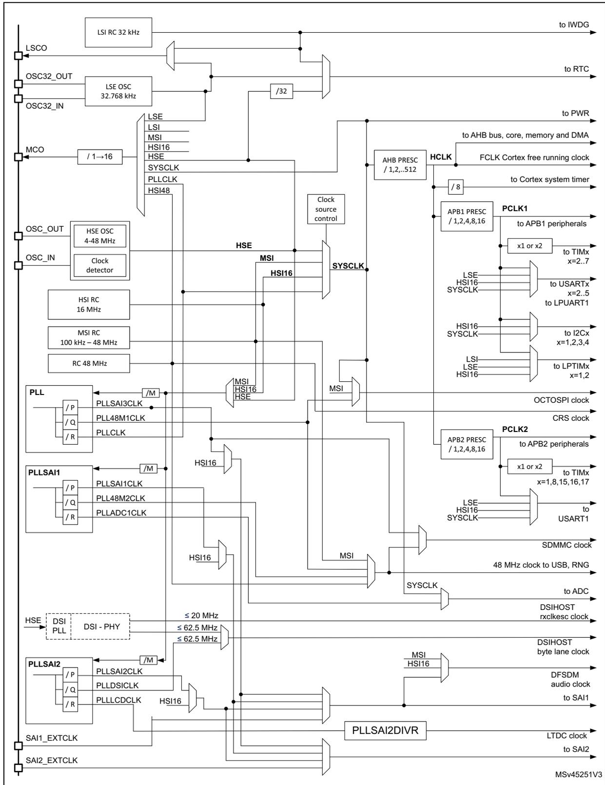
The diagram illustrates the clock architecture for STM32L4Rxxx and STM32L4Sxxx devices. It shows the flow of clock signals from various sources to different system components.
- External Oscillators:
- HSE (High-Speed External): Input via OSC32_IN, output via OSC32_OUT. Frequency range: 4-48 MHz. It can be used as a system clock (SYSCLK) or for the PLL.
- LSE (Low-Speed External): Input via OSC32_IN, output via OSC32_OUT. Frequency: 32.768 kHz. It can be used for the RTC or as a system clock (SYSCLK).
- Internal Oscillators:
- LSI (Low-Speed Internal): Frequency: 32 kHz. It can be used for the IWDG or as a system clock (SYSCLK).
- MSI (Multi-Speed Internal): Frequency range: 100 kHz to 48 MHz. It can be used as a system clock (SYSCLK).
- HSI (High-Speed Internal): Frequency: 16 MHz. It can be used as a system clock (SYSCLK).
- RC (Resistor-Capacitor): Frequency: 48 MHz. It can be used as a system clock (SYSCLK).
- PLL (Phase-Locked Loop):
- Input sources: HSE, MSI, HSI16.
- Outputs: PLLSAI3CLK, PLL48M1CLK, PLLCLK.
- PLLSAI1:
- Input source: HSI16.
- Outputs: PLLSAI1CLK, PLL48M2CLK, PLLADC1CLK.
- PLLSAI2:
- Input source: HSI16.
- Outputs: PLLSAI2CLK, PLLDSICLK, PLLLCDCLK.
- DSI PHY:
- Input source: HSE.
- Outputs: DSIHOST rxclkesc clock, DSIHOST byte lane clock.
- System Clock (SYSCLK):
The main clock for the system, derived from HSE, LSE, MSI, HSI, or PLL. It is distributed to:
- AHB bus, core, memory and DMA.
- APB1 and APB2 peripherals via PCLK1 and PCLK2 respectively.
- USB, RNG, SDMMC, and ADC.
- Other Clocks:
- HCLK: AHB clock, derived from SYSCLK with a prescaler (1/2 to 1/512). It is used for the Cortex system timer.
- PCLK1: APB1 clock, derived from HCLK with a prescaler (1/2 to 1/16). It is used for APB1 peripherals, TIMx, USARTx, LPUART1, I2Cx, and LPTIMx.
- PCLK2: APB2 clock, derived from HCLK with a prescaler (1/2 to 1/16). It is used for APB2 peripherals, TIMx, USART1, and SDMMC.
- MSv45251V3: A specific clock output.
- 1. For full details about the internal and external clock source characteristics, please refer to the “Electrical characteristics” section in your device datasheet.
- 2. The ADC clock can be derived from the AHB clock of the ADC bus interface, divided by a programmable factor (1, 2 or 4). When the programmable factor is ‘1’, the AHB prescaler must be equal to ‘1’.
Figure 17. DSI clock tree
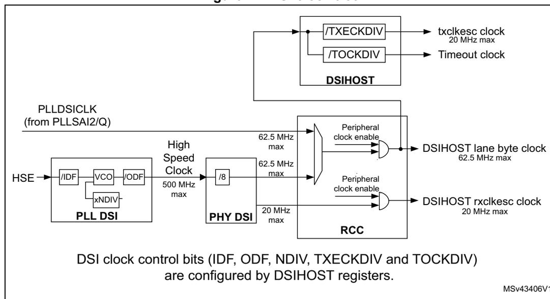
The diagram illustrates the DSI clock tree. It starts with the HSE (High Speed External) clock input to the PLL DSI block. The PLL DSI block contains an /IDF (Input Divider), a VCO (Voltage Controlled Oscillator), an /ODF (Output Divider), and an xNDIV (Multiplier). The output of the PLL DSI is the High Speed Clock (500 MHz max). This clock is then divided by 8 in the PHY DSI block to produce a 62.5 MHz max clock. The PLL DSI also receives PLLDSICLK (from PLLSAI2/Q) as an input. The PHY DSI block outputs a 20 MHz max clock. The RCC (Reset and Clock Control) block receives the 62.5 MHz max clock and the 20 MHz max clock. It contains two AND gates. The first AND gate takes the 62.5 MHz max clock and a 'Peripheral clock enable' signal to produce the DSIHOST lane byte clock (62.5 MHz max). The second AND gate takes the 20 MHz max clock and a 'Peripheral clock enable' signal to produce the DSIHOST rxclkesc clock (20 MHz max). The DSIHOST block contains /TXECKDIV and /TOCKDIV dividers. The /TXECKDIV divider takes the 20 MHz max clock and produces the txclkesc clock (20 MHz max). The /TOCKDIV divider takes the 20 MHz max clock and produces the Timeout clock.
DSI clock control bits (IDF, ODF, NDIV, TXECKDIV and TOCKDIV) are configured by DSIHOST registers.
MSV43406V1
Figure 18. Clock tree for STM32L4P5xx and STM32L4Q5xx devices
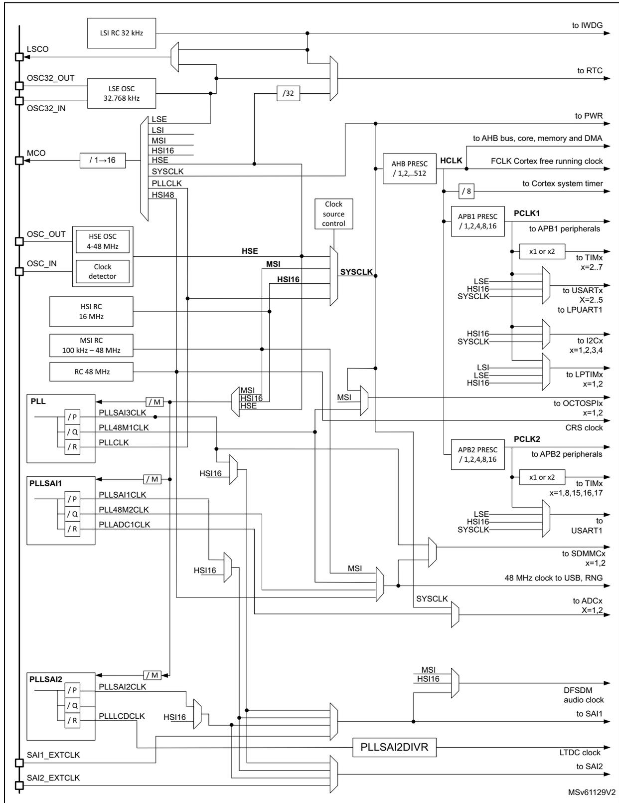
The diagram illustrates the clock tree architecture for STM32L4P5xx and STM32L4Q5xx devices. It shows the following components and connections:
- External Oscillators:
- LSI RC 32 kHz: Connected to LSCO pin and to IWDG.
- LSE OSC 32.768 kHz: Connected to OSC32_IN and OSC32_OUT pins. Output is divided by 32 (/32) and connected to RTC and PWR.
- HSE OSC 4-48 MHz: Connected to OSC_IN and OSC_OUT pins. Output is connected to a clock detector and the PLL.
- Internal Oscillators:
- HSI RC 16 MHz: Connected to the PLL and the HSI16 divider.
- MSI RC 100 kHz – 48 MHz: Connected to the PLL and the MSI divider.
- RC 48 MHz: Connected to the PLL and the HSI16 divider.
- PLL (Phase-Locked Loop):
- Inputs: HSE, HSI16, MSI, or HSE (via a multiplexer).
- Dividers: /M (input), /P, /Q, /R (output).
- Outputs: PLLSAI3CLK, PLL48M1CLK, PLLCLK.
- PLLSAI1:
- Input: PLLCLK.
- Dividers: /P, /Q, /R.
- Outputs: PLLSAI1CLK, PLL48M2CLK, PLLADC1CLK.
- PLLSAI2:
- Inputs: PLLSAI2CLK, PLLCDCLK, HSI16.
- Dividers: /M (input), /P, /Q, /R.
- Output: PLLSAI2CLK.
- PLLSAI2DIVR: Receives PLLSAI2CLK and provides the LTDC clock to SAI2.
- Clock Source Control: A central block that selects the system clock (SYSCLK) from LSE, LSI, MSI, HSI16, HSE, PLLCLK, or HSI48.
- System Clock (SYSCLK): The main clock for the system, derived from the selected source.
- Prescalers:
- AHB PRESC /1,2,..512: Divides SYSCLK to produce HCLK (FCLK Cortex free running clock) for the AHB bus, core, memory, and DMA. HCLK is also divided by 8 for the Cortex system timer.
- APB1 PRESC /1,2,4,8,16: Divides HCLK to produce PCLK1 for APB1 peripherals. PCLK1 is further divided by x1 or x2 for TIMx (x=2..7), USARTx (x=2..5) to LPUART1, I2Cx (x=1,2,3,4), and LPTIMx (x=1,2).
- APB2 PRESC /1,2,4,8,16: Divides HCLK to produce PCLK2 for APB2 peripherals. PCLK2 is further divided by x1 or x2 for TIMx (x=1,8,15,16,17), USART1, SDMMCx (x=1,2), and ADCx (x=1,2).
- Other Connections:
- MSI and HSI16 are used for the CRS clock.
- MSI and HSI16 are used for the 48 MHz clock to USB, RNG.
- MSI and HSI16 are used for the DFSDM audio clock to SAI1.
- SAI1_EXTCLK and SAI2_EXTCLK are connected to the PLLSAI2DIVR output.
6.2.1 HSE clock
The high speed external clock signal (HSE) can be generated from two possible clock sources:
- • HSE external crystal/ceramic resonator
- • HSE user external clock
The resonator and the load capacitors have to be placed as close as possible to the oscillator pins in order to minimize output distortion and startup stabilization time. The loading capacitance values must be adjusted according to the selected oscillator.
Figure 19. HSE/ LSE clock sources
| Clock source | Hardware configuration |
|---|---|
| External clock | 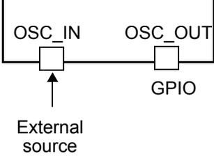 The diagram shows a block representing the microcontroller with two pins labeled OSC_IN and OSC_OUT. An external clock source is connected to the OSC_IN pin. The OSC_OUT pin is connected to a GPIO pin. |
| Crystal/Ceramic resonators | 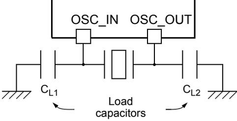 The diagram shows a block representing the microcontroller with two pins labeled OSC_IN and OSC_OUT. A crystal/ceramic resonator is connected between these two pins. Two load capacitors, labeled C L1 and C L2 , are connected from the OSC_IN and OSC_OUT pins respectively to ground. The capacitors are labeled 'Load capacitors'. |
External crystal/ceramic resonator (HSE crystal)
The 4 to 48 MHz external oscillator has the advantage of producing a very accurate rate on the main clock.
The associated hardware configuration is shown in Figure 19 . Refer to the electrical characteristics section of the datasheet for more details.
The HSERDY flag in the Clock control register (RCC_CR) indicates if the HSE oscillator is stable or not. At startup, the clock is not released until this bit is set by hardware. An interrupt can be generated if enabled in the Clock interrupt enable register (RCC_CIER) .
The HSE Crystal can be switched on and off using the HSEON bit in the Clock control register (RCC_CR) .
External source (HSE bypass)
In this mode, an external clock source must be provided. It can have a frequency of up to 48 MHz. You select this mode by setting the HSEBYP and HSEON bits in the Clock control register (RCC_CR) . The external clock signal (square, sinus or triangle) with ~40-60 % duty cycle depending on the frequency (refer to the datasheet ) has to drive the OSC_IN pin while the OSC_OUT pin can be used a GPIO. See Figure 19 .
6.2.2 HSI16 clock
The HSI16 clock signal is generated from an internal 16 MHz RC Oscillator.
The HSI16 RC oscillator has the advantage of providing a clock source at low cost (no external components). It also has a faster startup time than the HSE crystal oscillator however, even with calibration the frequency is less accurate than an external crystal oscillator or ceramic resonator.
The HSI16 clock can be selected as system clock after wakeup from Stop modes (Stop 0, Stop 1 or Stop 2). Refer to Section 6.3: Low-power modes . It can also be used as a backup clock source (auxiliary clock) if the HSE crystal oscillator fails. Refer to Section 6.2.10: Clock security system (CSS) .
Calibration
RC oscillator frequencies can vary from one chip to another due to manufacturing process variations, this is why each device is factory calibrated by ST for 1 % accuracy at \( T_A=25^\circ\text{C} \) .
After reset, the factory calibration value is loaded in the HSICAL[7:0] bits in the Internal clock sources calibration register (RCC_ICSCR) .
If the application is subject to voltage or temperature variations this may affect the RC oscillator speed. You can trim the HSI16 frequency in the application using the HSITRIM[6:0] in the Internal clock sources calibration register (RCC_ICSCR) .
For more details on how to measure the HSI16 frequency variation, refer to Section 6.2.17: Internal/external clock measurement with TIM15/TIM16/TIM17 .
The HSIRDY flag in the Clock control register (RCC_CR) indicates if the HSI16 RC is stable or not. At startup, the HSI16 RC output clock is not released until this bit is set by hardware.
The HSI16 RC can be switched on and off using the HSION bit in the Clock control register (RCC_CR) .
The HSI16 signal can also be used as a backup source (Auxiliary clock) if the HSE crystal oscillator fails. Refer to Section 6.2.10: Clock security system (CSS) on page 253 .
6.2.3 MSI clock
The MSI clock signal is generated from an internal RC oscillator. Its frequency range can be adjusted by software by using the MSIRANGE[3:0] bits in the Clock control register (RCC_CR) . Twelve frequency ranges are available: 100 kHz, 200 kHz, 400 kHz, 800 kHz, 1 MHz, 2 MHz, 4 MHz (default value), 8 MHz, 16 MHz, 24 MHz, 32 MHz and 48 MHz.
The MSI clock is used as system clock after restart from Reset, wakeup from Standby and Shutdown low-power modes. After restart from Reset, the MSI frequency is set to its default value 4 MHz. Refer to Section 6.3: Low-power modes .
The MSI clock can be selected as system clock after a wakeup from Stop mode (Stop 0, Stop 1 or Stop 2). Refer to Section 6.3: Low-power modes . It can also be used as a backup clock source (auxiliary clock) if the HSE crystal oscillator fails. Refer to Section 6.2.10: Clock security system (CSS) .
The MSI RC oscillator has the advantage of providing a low-cost (no external components) low-power clock source. In addition, when used in PLL-mode with the LSE, it provides a very accurate clock source which can be used by the USB OTG FS device, and feed the main PLL to run the system at the maximum speed.
The MSIRDY flag in the Clock control register (RCC_CR) indicates whether the MSI RC is stable or not. At startup, the MSI RC output clock is not released until this bit is set by hardware. The MSI RC can be switched on and off by using the MSION bit in the Clock control register (RCC_CR) .
Hardware auto calibration with LSE (PLL-mode)
When a 32.768 kHz external oscillator is present in the application, it is possible to configure the MSI in a PLL-mode by setting the MSIPLLEN bit in the Clock control register (RCC_CR) . When configured in PLL-mode, the MSI automatically calibrates itself thanks to the LSE. This mode is available for all MSI frequency ranges. At 48 MHz, the MSI in PLL-mode can be used for the USB OTG FS device, saving the need of an external high-speed crystal.
Software calibration
The MSI RC oscillator frequency can vary from one chip to another due to manufacturing process variations, this is why each device is factory calibrated by ST for 1 % accuracy at an ambient temperature, TA, of 25 °C. After reset, the factory calibration value is loaded in the MSICAL[7:0] bits in the Internal clock sources calibration register (RCC_ICSCR) . If the application is subject to voltage or temperature variations, this may affect the RC oscillator speed. You can trim the MSI frequency in the application by using the MSITRIM[7:0] bits in the RCC_ICSCR register. For more details on how to measure the MSI frequency variation please refer to Section 6.2.17: Internal/external clock measurement with TIM15/TIM16/TIM17 .
6.2.4 HSI48 clock
The HSI48 clock signal is generated from an internal 48 MHz RC oscillator and can be used directly for USB and for random number generator (RNG) as well as SDMMC.
The internal 48 MHz RC oscillator is mainly dedicated to provide a high precision clock to the USB peripheral by means of a special Clock Recovery System (CRS) circuitry. The CRS
can use the USB SOF signal, the LSE or an external signal to automatically and quickly adjust the oscillator frequency on-fly. It is disabled as soon as the system enters Stop or Standby mode. When the CRS is not used, the HSI48 RC oscillator runs on its default frequency which is subject to manufacturing process variations.
For more details on how to configure and use the CRS peripheral please refer to Section 7: Clock recovery system (CRS) .
The HSI48RDY flag in the Clock recovery RC register (RCC_CRRRCR) indicates whether the HSI48 RC oscillator is stable or not. At startup, the HSI48 RC oscillator output clock is not released until this bit is set by hardware.
The HSI48 can be switched on and off using the HSI48ON bit in the Clock recovery RC register (RCC_CRRRCR).
6.2.5 PLL
The device embeds 3 PLLs: PLL, PLLSAI1, PLLSAI2. Each PLL provides up to three independent outputs. The internal PLLs can be used to multiply the HSI16, HSE or MSI output clock frequency. The PLLs input frequency must be between 4 and 16 MHz. The selected clock source is divided by a programmable factor PLLM from 1 to 8 to provide a clock frequency in the requested input range. Refer to Figure 16: Clock tree for STM32L4Rxxx and STM32L4Sxxx devices and PLL configuration register (RCC_PLLCFGR) .
The PLLs configuration (selection of the input clock and multiplication factor) must be done before enabling the PLL. Once the PLL is enabled, these parameters cannot be changed.
To modify the PLL configuration, proceed as follows:
- 1. Disable the PLL by setting PLLON to 0 in Clock control register (RCC_CR) .
- 2. Wait until PLLRDY is cleared. The PLL is now fully stopped.
- 3. Change the desired parameter.
- 4. Enable the PLL again by setting PLLON to 1.
- 5. Enable the desired PLL outputs by configuring PLLPEN, PLLQEN, PLLREN in PLL configuration register (RCC_PLLCFGR) .
An interrupt can be generated when the PLL is ready, if enabled in the Clock interrupt enable register (RCC_CIER) .
The same procedure is applied for changing the configuration of the PLLSAI1 or PLLSAI2:
- 1. Disable the PLLSAI1/PLLSAI2 by setting PLLSAI1ON/PLLSAI2ON to 0 in Clock control register (RCC_CR) .
- 2. Wait until PLLSAI1RDY/PLLSAI2RDY is cleared. The PLLSAI1/PLLSAI2 is now fully stopped.
- 3. Change the desired parameter.
- 4. Enable the PLLSAI1/PLLSAI2 again by setting PLLSAI1ON/PLLSAI2ON to 1.
- 5. Enable the desired PLL outputs by configuring PLLSAI1PEN/PLLSAI2PEN, PLLSAI1QEN/PLLSAI2QEN, PLLSAI1REN/PLLSAI2REN in PLLSAI1 configuration register (RCC_PLLSAI1CFGR) and PLLSAI2 configuration register (RCC_PLLSAI2CFGR) .
The PLL output frequency must not exceed 120 MHz.
The enable bit of each PLL output clock (PLLPEN, PLLQEN, PLLREN, PLLSAI1PEN, PLLSAI1QEN, PLLSAI1REN, PLLSAI2PEN and PLLSAI2REN) can be modified at any time without stopping the corresponding PLL. PLLREN cannot be cleared if PLLCLK is used as system clock.
6.2.6 LSE clock
The LSE crystal is a 32.768 kHz Low Speed External crystal or ceramic resonator. It has the advantage of providing a low-power but highly accurate clock source to the real-time clock peripheral (RTC) for clock/calendar or other timing functions.
The LSE crystal is switched on and off using the LSEON bit in Backup domain control register (RCC_BDCR) . The crystal oscillator driving strength can be changed at runtime using the LSEDRV[1:0] bits in the Backup domain control register (RCC_BDCR) to obtain the best compromise between robustness and short start-up time on one side and low-power-consumption on the other side. The LSE drive can be decreased to the lower drive capability (LSEDRV=00) when the LSE is ON. However, once LSEDRV is selected, the drive capability can not be increased if LSEON=1.
The LSERDY flag in the Backup domain control register (RCC_BDCR) indicates whether the LSE crystal is stable or not. At startup, the LSE crystal output clock signal is not released until this bit is set by hardware. An interrupt can be generated if enabled in the Clock interrupt enable register (RCC_CIER) .
Distribution of the external 32 kHz clock (LSE) outside the RTC block could be disabled by setting LSESYSDIS bit in Backup domain control register (RCC_BDCR) to reduce power consumption. Propagation is stopped regardless the use of LSE by other peripherals. This feature is present only on STM32L4P5xx and STM32L4Q5xx devices.
External source (LSE bypass)
In this mode, an external clock source must be provided. It can have a frequency of up to 1 MHz. You select this mode by setting the LSEBYP and LSEON bits in the AHB1 peripheral clocks enable in Sleep and Stop modes register (RCC_AHB1SMENR) . The external clock signal (square, sinus or triangle) with ~50 % duty cycle has to drive the OSC32_IN pin while the OSC32_OUT pin can be used as GPIO. See Figure 19 .
6.2.7 LSI clock
The LSI RC acts as a low-power clock source that can be kept running in Stop and Standby mode for the independent watchdog (IWDG) RTC. The clock frequency is 32 kHz. For more details, refer to the electrical characteristics section of the datasheets.
The LSI RC can be switched on and off using the LSION bit in the Control/status register (RCC_CSR) .
The LSIRDY flag in the Control/status register (RCC_CSR) indicates if the LSI oscillator is stable or not. At startup, the clock is not released until this bit is set by hardware. An interrupt can be generated if enabled in the Clock interrupt enable register (RCC_CIER) .
6.2.8 System clock (SYSCLK) selection
Four different clock sources can be used to drive the system clock (SYSCLK):
- • MSI oscillator
- • HSI16 oscillator
- • HSE oscillator
- • PLL
The system clock maximum frequency is 120 MHz. After a system reset, the MSI oscillator, at 4 MHz, is selected as system clock. When a clock source is used directly or through the PLL as a system clock, it is not possible to stop it.
A switch from one clock source to another occurs only if the target clock source is ready (clock stable after startup delay or PLL locked). If a clock source which is not yet ready is selected, the switch will occur when the clock source becomes ready. Status bits in the Internal clock sources calibration register (RCC_ICSCR) indicate which clock(s) is (are) ready and which clock is currently used as a system clock.
To switch from low speed to high speed or from high speed to low speed system clock, it is recommended to use a transition state with medium speed clock, for at least 1us.
Clock source switching conditions:
- • Switching from HSE or HSI or MSI to PLL with AHB frequency (HCLK) higher than 80 MHz
- • Switching from PLL with HCLK higher than 80 MHz to HSE or HSI or MSI
Transition state:
- • Set the AHB prescaler HPRE[3:0] bits to divide the system frequency by 2
- • Switch system clock to PLL
- • Wait for at least 1us and then reconfigure AHB prescaler bits to the needed HCLK frequency
6.2.9 Clock source frequency versus voltage scaling
The following table gives the different clock source frequencies depending on the product voltage range.
Table 37. Clock source frequency
| Product voltage range | Clock frequency | |||
|---|---|---|---|---|
| MSI | HSI16 | HSE | PLL/PLL1/PLL2 | |
| Range 1 Boost mode | 48 MHz | 16 MHz | 48 MHz | 120 MHz |
| Range 1 Normal mode | 48 MHz | 16 MHz | 48 MHz | 80 MHz |
| Range 2 | 24 MHz range | 16 MHz | 26 MHz | 26 MHz |
6.2.10 Clock security system (CSS)
Clock Security System can be activated by software. In this case, the clock detector is enabled after the HSE oscillator startup delay, and disabled when this oscillator is stopped.
If a failure is detected on the HSE clock, the HSE oscillator is automatically disabled, a clock failure event is sent to the break input of the advanced-control timers (TIM1/TIM8 and TIM15/16/17) and an interrupt is generated to inform the software about the failure (Clock Security System Interrupt CSSI), allowing the MCU to perform rescue operations. The CSSI is linked to the Cortex®-M4 NMI (Non-Maskable Interrupt) exception vector.
Note: Once the CSS is enabled and if the HSE clock fails, the CSS interrupt occurs and a NMI is automatically generated. The NMI will be executed indefinitely unless the CSS interrupt pending bit is cleared. As a consequence, in the NMI ISR user must clear the CSS interrupt by setting the CSSC bit in the Clock interrupt clear register (RCC_CICR) .
If the HSE oscillator is used directly or indirectly as the system clock (indirectly means: it is used as PLL input clock, and the PLL clock is used as system clock), a detected failure causes a switch of the system clock to the MSI or the HSI16 oscillator depending on the STOPWUCK configuration in the Clock configuration register (RCC_CFGR) , and the disabling of the HSE oscillator. If the HSE clock (divided or not) is the clock entry of the PLL used as system clock when the failure occurs, the PLL is disabled too.
6.2.11 Clock security system on LSE
A Clock Security System on LSE can be activated by software writing the LSECSSON bit in the Backup domain control register (RCC_BDCR) . This bit can be disabled only by a hardware reset or RTC software reset, or after a failure detection on LSE. LSECSSON must be written after LSE and LSI are enabled (LSEON and LSION enabled) and ready (LSERDY and LSIRDY set by hardware), and after the RTC clock has been selected by RTCSEL and LSIPREDIV is disabled.
Note: LSIPREDIV bit is available only on STM32L4P5xx and STM32L4Q5xx devices.
The CSS on LSE is working in all modes except VBAT. It is working also under system reset (excluding power on reset). If a failure is detected on the external 32 kHz oscillator, the LSE clock is no longer supplied to the RTC but no hardware action is made to the registers. If the MSI was in PLL-mode, this mode is disabled.
In Standby mode a wakeup is generated. In other modes an interrupt can be sent to wakeup the software (see Clock interrupt enable register (RCC_CIER) , Clock interrupt flag register (RCC_CIFR) , Clock interrupt clear register (RCC_CICR) ).
The software MUST then disable the LSECSSON bit, stop the defective 32 kHz oscillator (disabling LSEON), and change the RTC clock source (no clock or LSI or HSE, with RTCSEL), or take any required action to secure the application.
The frequency of LSE oscillator have to be higher than 30 kHz to avoid false positive CSS detection.
6.2.12 ADC clock
The ADC clock is derived from the system clock, or from the PLLSAI1 output. It can reach 120 MHz and can be divided by the following prescalers values:
1,2,4,6,8,10,12,16,32,64,128 or 256 by configuring the ADC1_CCR register. It is asynchronous to the AHB clock. Alternatively, the ADC clock can be derived from the AHB clock of the ADC bus interface, divided by a programmable factor (1, 2 or 4). This programmable factor is configured using the CKMODE bit fields in the ADC123_CCR.
If the programmed factor is '1', the AHB prescaler must be set to '1'.
6.2.13 RTC clock
The RTCCLK clock source can be either the HSE/32, LSE or LSI clock. It is selected by programming the RTCSEL[1:0] bits in the Backup domain control register (RCC_BDCR) . This selection cannot be modified without resetting the Backup domain. The system must always be configured so as to get a PCLK frequency greater than or equal to the RTCCLK frequency for a proper operation of the RTC.
The LSE clock is in the Backup domain, whereas the HSE and LSI clocks are not. Consequently:
- • If LSE is selected as RTC clock:
- – The RTC continues to work even if the \( V_{DD} \) supply is switched off, provided the \( V_{BAT} \) supply is maintained.
- • If LSI is selected as the RTC clock:
- – The RTC state is not guaranteed if the \( V_{DD} \) supply is powered off.
- • If the HSE clock divided by a prescaler is used as the RTC clock:
- – The RTC state is not guaranteed if the \( V_{DD} \) supply is powered off or if the internal voltage regulator is powered off (removing power from the \( V_{CORE} \) domain).
When the RTC clock is LSE or LSI, the RTC remains clocked and functional under system reset.
6.2.14 Timer clock
The timer clock frequencies are automatically defined by hardware. There are two cases:
- 1. If the APB prescaler equals 1, the timer clock frequencies are set to the same frequency as that of the APB domain.
- 2. Otherwise, they are set to twice ( \( \times 2 \) ) the frequency of the APB domain.
6.2.15 Watchdog clock
If the Independent watchdog (IWDG) is started by either hardware option or software access, the LSI oscillator is forced ON and cannot be disabled. After the LSI oscillator temporization, the clock is provided to the IWDG.
6.2.16 Clock-out capability
- • MCO
The microcontroller clock output (MCO) capability allows the clock to be output onto the external MCO pin. One of eight clock signals can be selected as the MCO clock.
- – LSI
- – LSE
- – SYSCLK
- – HSI16
- – HSI48
- – HSE
- – PLLCLK
- – MSI
The selection is controlled by the MCOSEL[3:0] bits of the Clock configuration register (RCC_CFGR) . The selected clock can be divided with the MCOPRE[2:0] field of the Clock configuration register (RCC_CFGR) .
- • LSCO
Another output (LSCO) allows a low speed clock to be output onto the external LSCO pin:
- – LSI
- – LSE
This output remains available in Stop (Stop 0, Stop 1 and Stop 2) and Standby modes. The selection is controlled by the LSCOSEL, and enabled with the LSCOEN in the Backup domain control register (RCC_BDCR) .
The MCO clock output requires the corresponding alternate function selected on the MCO pin, the LSCO pin should be left in default POR state.
6.2.17 Internal/external clock measurement with TIM15/TIM16/TIM17
It is possible to indirectly measure the frequency of all on-board clock sources by mean of the TIM15, TIM16 or TIM17 channel 1 input capture, as represented on Figure 20 , Figure 21 and Figure 22 .
Figure 20. Frequency measurement with TIM15 in capture mode
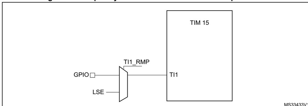
The diagram shows a 'TIM 15' block on the right. Its 'TI1' pin is connected to the output of a multiplexer. The multiplexer has two inputs: 'GPIO' and 'LSE'. The output of the multiplexer is labeled 'TI1_RMP' and is connected to the 'TI1' pin of the 'TIM 15' block. The diagram is labeled 'MS33433V1' in the bottom right corner.
The input capture channel of the Timer 15 can be a GPIO line or an internal clock of the MCU. This selection is performed through the TI1_RMP bit in the TIM15_OR register. The possibilities are the following ones:
- • TIM15 Channel1 is connected to the GPIO. Refer to the alternate function mapping in the device datasheets.
- • TIM15 Channel1 is connected to the LSE.
Figure 21. Frequency measurement with TIM16 in capture mode
![Diagram of TIM16 input capture mode showing a multiplexer selecting between various internal clock sources (LSI, LSE, RTC wakeup interrupt, MSI, HSE/32, MCO, NC) and a GPIO for the TI1 input. The selection is controlled by the TI1_RMP[1:0] bits. The diagram is labeled MSv63428V1.](/RM0432-STM32L4+/541655d4f95469ae7bd325a7140c6061_img.jpg)
The input capture channel of the Timer 16 can be a GPIO line or an internal clock of the MCU. This selection is performed through the TI1_RMP[1:0] bits in the TIM16_OR register. The possibilities are the following ones:
- • TIM16 Channel1 is connected to the GPIO. Refer to the alternate function mapping in the device datasheets.
- • TIM16 Channel1 is connected to the LSI clock.
- • TIM16 Channel1 is connected to the LSE clock.
- • TIM16 Channel1 is connected to the RTC wakeup interrupt signal. In this case the RTC interrupt should be enabled.
- • TIM16 Channel1 is connected to the MSI clock.
- • TIM16 Channel1 is connected to the HSE/32 clock.
- • TIM16 Channel1 is connected to the MCO clock.
Figure 22. Frequency measurement with TIM17 in capture mode
![Diagram of TIM17 input capture mode showing a multiplexer selecting between MSI, HSE/32, and MCO internal clock sources and a GPIO for the TI1 input. The selection is controlled by the TI1_RMP[1:0] bits. The diagram is labeled MS33435V1.](/RM0432-STM32L4+/e1707f28295a8400ab19c74046b0ede4_img.jpg)
The input capture channel of the Timer 17 can be a GPIO line or an internal clock of the MCU. This selection is performed through the TI1_RMP[1:0] bits in the TIM17_OR register. The possibilities are the following ones:
- • TIM17 Channel1 is connected to the GPIO. Refer to the alternate function mapping in the device datasheets.
- • TIM17 Channel1 is connected to the MSI Clock.
- • TIM17 Channel1 is connected to the HSE/32 Clock.
- • TIM17 Channel1 is connected to the microcontroller clock output (MCO), this selection is controlled by the MCOSEL[3:0] bits of the Clock configuration register (RCC_CFGR).
Calibration of the HSI16 and the MSI
For TIM15 and TIM16, the primary purpose of connecting the LSE to the channel 1 input capture is to be able to precisely measure the HSI16 and MSI system clocks (for this, either the HSI16 or MSI should be used as the system clock source). The number of HSI16 (MSI, respectively) clock counts between consecutive edges of the LSE signal provides a measure of the internal clock period. Taking advantage of the high precision of LSE crystals (typically a few tens of ppm's), it is possible to determine the internal clock frequency with the same resolution, and trim the source to compensate for manufacturing, process, temperature and/or voltage related frequency deviations.
The MSI and HSI16 oscillator both have dedicated user-accessible calibration bits for this purpose.
The basic concept consists in providing a relative measurement (e.g. the HSI16/LSE ratio): the precision is therefore closely related to the ratio between the two clock sources. The higher the ratio is, the better the measurement will be.
If LSE is not available, HSE/32 will be the better option in order to reach the most precise calibration possible.
It is however not possible to have a good enough resolution when the MSI clock is low (typically below 1 MHz). In this case, it is advised to:
- • accumulate the results of several captures in a row
- • use the timer's input capture prescaler (up to 1 capture every 8 periods)
- • use the RTC wakeup interrupt signal (when the RTC is clocked by the LSE) as the input for the channel1 input capture. This improves the measurement precision. For this purpose the RTC wakeup interrupt must be enable.
Calibration of the LSI
The calibration of the LSI will follow the same pattern that for the HSI16, but changing the reference clock. It will be necessary to connect LSI clock to the channel 1 input capture of the TIM16. Then define the HSE as system clock source, the number of his clock counts between consecutive edges of the LSI signal provides a measure of the internal low speed clock period.
The basic concept consists in providing a relative measurement (e.g. the HSE/LSI ratio): the precision is therefore closely related to the ratio between the two clock sources. The higher the ratio is, the better the measurement will be.
6.2.18 Peripheral clock enable register (RCC_AHBxENR, RCC_APBxENRy)
Each peripheral clock can be enabled by the xxxxEN bit of the RCC_AHBxENR, RCC_APBxENRy registers.
When the peripheral clock is not active, the peripheral registers read or write accesses are not supported.
The enable bit has a synchronization mechanism to create a glitch free clock for the peripheral. After the enable bit is set, there is a 2 clock cycles delay before the clock be active.
Caution: Just after enabling the clock for a peripheral, software must wait for a delay before accessing the peripheral registers.
6.3 Low-power modes
- • AHB and APB peripheral clocks, including DMA clock, can be disabled by software.
- • Sleep and Low Power Sleep modes stops the CPU clock. The memory interface clocks (Flash, SRAM1, SRAM2 and SRAM3 interfaces) can be stopped by software during sleep mode. The AHB to APB bridge clocks are disabled by hardware during Sleep mode when all the clocks of the peripherals connected to them are disabled.
- • Stop modes (Stop 0, Stop 1 and Stop 2) stops all the clocks in the V CORE domain and disables the three PLL, the HSI16, the MSI and the HSE oscillators.
All U(S)ARTs, LPUARTs and I 2 Cs have the capability to enable the HSI16 oscillator even when the MCU is in Stop mode (if HSI16 is selected as the clock source for that peripheral).
All U(S)ARTs and LPUARTs can also be driven by the LSE oscillator when the system is in Stop mode (if LSE is selected as clock source for that peripheral) and the LSE oscillator is enabled (LSEON). In that case the LSE remains always ON in Stop mode (they do not have the capability to turn on the LSE oscillator).
- • Standby and Shutdown modes stops all the clocks in the V CORE domain and disables the PLL, the HSI16, the MSI and the HSE oscillators.
The CPU's deepsleep mode can be overridden for debugging by setting the DBG_STOP or DBG_STANDBY bits in the DBGMCU_CR register.
When leaving the Stop modes (Stop 0, Stop 1 or Stop 2), the system clock is either MSI or HSI16, depending on the software configuration of the STOPWUCK bit in the RCC_CFGR register. The frequency (range and user trim) of the MSI oscillator is the one configured before entering Stop mode. The user trim of HSI16 is kept. If the MSI was in PLL-mode before entering Stop mode, the PLL-mode stabilization time must be waited for after wakeup even if the LSE was kept ON during the Stop mode.
When leaving the Standby and Shutdown modes, the system clock is MSI. The MSI frequency at wakeup from Standby mode is configured with the MSISRANGE in the RCC_CSR register, from 1 to 8 MHz. The MSI frequency at wakeup from Shutdown mode is 4 MHz. The user trim is lost.
If a Flash memory programming operation is on going, Stop, Standby and Shutdown modes entry is delayed until the Flash memory interface access is finished. If an access to the APB domain is ongoing, Stop, Standby and Shutdown modes entry is delayed until the APB access is finished.
6.4 RCC registers
6.4.1 Clock control register (RCC_CR)
Address offset: 0x00
Reset value: 0x0000 0063. HSEBYP is not affected by reset.
Access: no wait state, word, half-word and byte access
| 31 | 30 | 29 | 28 | 27 | 26 | 25 | 24 | 23 | 22 | 21 | 20 | 19 | 18 | 17 | 16 |
|---|---|---|---|---|---|---|---|---|---|---|---|---|---|---|---|
| Res. | Res. | PLL2SAI2RDY | PLL2SAI2ON | PLL1SAI1RDY | PLL1SAI1ON | PLL2RDY | PLLON | Res. | Res. | Res. | Res. | CSSON | HSEBYP | HSE RDY | HSE ON |
| r | rw | r | rw | r | rw | rs | rw | r | rw | ||||||
| 15 | 14 | 13 | 12 | 11 | 10 | 9 | 8 | 7 | 6 | 5 | 4 | 3 | 2 | 1 | 0 |
| Res. | Res. | Res. | Res. | HSIASFS | HSIRDY | HSIKERON | HSION | MSIRANGE[3:0] | MSIRGSEL | MSIPLLEN | MSI RDY | MSION | |||
| rw | r | rw | rw | rw | rw | rw | rw | rs | rw | r | rw | ||||
Bits 31:30 Reserved, must be kept at reset value.
Bit 29 PLL2SAI2RDY : SAI2 PLL clock ready flag
Set by hardware to indicate that the PLL2SAI2 is locked.
0: PLL2SAI2 unlocked
1: PLL2SAI2 locked
Bit 28 PLL2SAI2ON : SAI2 PLL enable
Set and cleared by software to enable PLL2SAI2.
Cleared by hardware when entering Stop, Standby or Shutdown mode.
0: PLL2SAI2 OFF
1: PLL2SAI2 ON
Bit 27 PLL1SAI1RDY : SAI1 PLL clock ready flag
Set by hardware to indicate that the PLL1SAI1 is locked.
0: PLL1SAI1 unlocked
1: PLL1SAI1 locked
Bit 26 PLL1SAI1ON : SAI1 PLL enable
Set and cleared by software to enable PLL1SAI1.
Cleared by hardware when entering Stop, Standby or Shutdown mode.
0: PLL1SAI1 OFF
1: PLL1SAI1 ON
Bit 25 PLL2RDY : Main PLL clock ready flag
Set by hardware to indicate that the main PLL is locked.
0: PLL unlocked
1: PLL locked
Bit 24 PLLON : Main PLL enable
Set and cleared by software to enable the main PLL.
Cleared by hardware when entering Stop, Standby or Shutdown mode. This bit cannot be reset if the PLL clock is used as the system clock.
0: PLL OFF
1: PLL ON
Bits 23:20 Reserved, must be kept at reset value.
Bit 19 CSSON : Clock security system enableSet by software to enable the clock security system. When CSSON is set, the clock detector is enabled by hardware when the HSE oscillator is ready, and disabled by hardware if a HSE clock failure is detected. This bit is set only and is cleared by reset.
0: Clock security system OFF (clock detector OFF)
1: Clock security system ON (Clock detector ON if the HSE oscillator is stable, OFF if not).
Bit 18 HSEBYP : HSE crystal oscillator bypassSet and cleared by software to bypass the oscillator with an external clock. The external clock must be enabled with the HSEON bit set, to be used by the device. The HSEBYP bit can be written only if the HSE oscillator is disabled.
0: HSE crystal oscillator not bypassed
1: HSE crystal oscillator bypassed with external clock
Bit 17 HSERDY : HSE clock ready flagSet by hardware to indicate that the HSE oscillator is stable.
0: HSE oscillator not ready
1: HSE oscillator ready
Note: Once the HSEON bit is cleared, HSERDY goes low after 6 HSE clock cycles.
Bit 16 HSEON : HSE clock enableSet and cleared by software.
Cleared by hardware to stop the HSE oscillator when entering Stop, Standby or Shutdown mode. This bit cannot be reset if the HSE oscillator is used directly or indirectly as the system clock.
0: HSE oscillator OFF
1: HSE oscillator ON
Bits 15:12 Reserved, must be kept at reset value.
Bit 11 HSIASFS : HSI16 automatic start from StopSet and cleared by software. When the system wakeup clock is MSI, this bit is used to wakeup the HSI16 in parallel of the system wakeup.
0: HSI16 oscillator is not enabled by hardware when exiting Stop mode with MSI as wakeup clock.
1: HSI16 oscillator is enabled by hardware when exiting Stop mode with MSI as wakeup clock.
Bit 10 HSIRDY : HSI16 clock ready flagSet by hardware to indicate that HSI16 oscillator is stable. This bit is set only when HSI16 is enabled by software by setting HSION.
0: HSI16 oscillator not ready
1: HSI16 oscillator ready
Note: Once the HSION bit is cleared, HSIRDY goes low after 6 HSI16 clock cycles.
Bit 9 HSIKERON : HSI16 always enable for peripheral kernels.Set and cleared by software to force HSI16 ON even in Stop modes. The HSI16 can only feed USARTs and I 2 Cs peripherals configured with HSI16 as kernel clock. Keeping the HSI16 ON in Stop mode allows to avoid slowing down the communication speed because of the HSI16 startup time. This bit has no effect on HSION value.
0: No effect on HSI16 oscillator.
1: HSI16 oscillator is forced ON even in Stop mode.
Bit 8 HSION : HSI16 clock enable
Set and cleared by software.
Cleared by hardware to stop the HSI16 oscillator when entering Stop, Standby or Shutdown mode.
Set by hardware to force the HSI16 oscillator ON when STOPWUCK=1 or HSIASFS = 1 when leaving Stop modes, or in case of failure of the HSE crystal oscillator.
This bit is set by hardware if the HSI16 is used directly or indirectly as system clock.
0: HSI16 oscillator OFF
1: HSI16 oscillator ON
Bits 7:4 MSIRANGE[3:0] : MSI clock ranges
These bits are configured by software to choose the frequency range of MSI when MSIRGSEL is set. 12 frequency ranges are available:
0000: range 0 around 100 kHz
0001: range 1 around 200 kHz
0010: range 2 around 400 kHz
0011: range 3 around 800 kHz
0100: range 4 around 1M Hz
0101: range 5 around 2 MHz
0110: range 6 around 4 MHz (reset value)
0111: range 7 around 8 MHz
1000: range 8 around 16 MHz
1001: range 9 around 24 MHz
1010: range 10 around 32 MHz
1011: range 11 around 48 MHz
others: not allowed (hardware write protection)
Note: Warning: MSIRANGE can be modified when MSI is OFF (MSION=0) or when MSI is ready (MSIRDY=1). MSIRANGE must NOT be modified when MSI is ON and NOT ready (MSION=1 and MSIRDY=0)
Bit 3 MSIRGSEL : MSI clock range selection
Set by software to select the MSI clock range with MSIRANGE[3:0]. Write 0 has no effect.
After a standby or a reset MSIRGSEL is at 0 and the MSI range value is provided by MSISRANGE in CSR register.
0: MSI Range is provided by MSISRANGE[3:0] in RCC_CSR register
1: MSI Range is provided by MSIRANGE[3:0] in the RCC_CR register
Bit 2 MSIPLLEN : MSI clock PLL enable
Set and cleared by software to enable/ disable the PLL part of the MSI clock source.
MSIPLLEN must be enabled after LSE is enabled (LSEON enabled) and ready (LSERDY set by hardware). There is a hardware protection to avoid enabling MSIPLLEN if LSE is not ready.
This bit is cleared by hardware when LSE is disabled (LSEON = 0) or when the Clock Security System on LSE detects a LSE failure (refer to RCC_CSR register).
0: MSI PLL OFF
1: MSI PLL ON
Bit 1 MSIRDY : MSI clock ready flag
This bit is set by hardware to indicate that the MSI oscillator is stable.
0: MSI oscillator not ready
1: MSI oscillator ready
Note: Once the MSION bit is cleared, MSIRDY goes low after 6 MSI clock cycles.
Bit 0 MSION : MSI clock enable
This bit is set and cleared by software.
Cleared by hardware to stop the MSI oscillator when entering Stop, Standby or Shutdown mode.
Set by hardware to force the MSI oscillator ON when exiting Standby or Shutdown mode.
Set by hardware to force the MSI oscillator ON when STOPWUCK=0 when exiting from Stop modes, or in case of a failure of the HSE oscillator
Set by hardware when used directly or indirectly as system clock.
0: MSI oscillator OFF
1: MSI oscillator ON
6.4.2 Internal clock sources calibration register (RCC_ICSCR)
Address offset: 0x04
Reset value: 0x40XX 00XX where X is factory-programmed.
Access: no wait state, word, half-word and byte access.
| 31 | 30 | 29 | 28 | 27 | 26 | 25 | 24 | 23 | 22 | 21 | 20 | 19 | 18 | 17 | 16 |
|---|---|---|---|---|---|---|---|---|---|---|---|---|---|---|---|
| Res. | HSITRIM[6:0] | HSICAL[7:0] | |||||||||||||
| rw | rw | rw | rw | rw | rw | rw | r | r | r | r | r | r | r | r | |
| 15 | 14 | 13 | 12 | 11 | 10 | 9 | 8 | 7 | 6 | 5 | 4 | 3 | 2 | 1 | 0 |
| MSITRIM[7:0] | MSICAL[7:0] | ||||||||||||||
| rw | rw | rw | rw | rw | rw | rw | rw | r | r | r | r | r | r | r | r |
Bit 31 Reserved, must be kept at reset value.
Bits 30:24 HSITRIM[6:0] : HSI16 clock trimming
These bits provide an additional user-programmable trimming value that is added to the HSICAL[7:0] bits. It can be programmed to adjust to variations in voltage and temperature that influence the frequency of the HSI16.
The default value is 16, which, when added to the HSICAL value, should trim the HSI16 to 16 MHz \( \pm \) 1 %.
Bits 23:16 HSICAL[7:0] : HSI16 clock calibration
These bits are initialized at startup with the factory-programmed HSI16 calibration trim value. When HSITRIM is written, HSICAL is updated with the sum of HSITRIM and the factory trim value.
Bits 15:8 MSITRIM[7:0] : MSI clock trimming
These bits provide an additional user-programmable trimming value that is added to the MSICAL[7:0] bits. It can be programmed to adjust to variations in voltage and temperature that influence the frequency of the MSI.
Bits 7:0 MSICAL[7:0] : MSI clock calibration
These bits are initialized at startup with the factory-programmed MSI calibration trim value. When MSITRIM is written, MSICAL is updated with the sum of MSITRIM and the factory trim value.
6.4.3 Clock configuration register (RCC_CFGR)
Address offset: 0x08
Reset value: 0x0000 0000
Access: \( 0 \leq \text{wait state} \leq 2 \) , word, half-word and byte access
1 or 2 wait states inserted only if the access occurs during clock source switch.
From 0 to 15 wait states inserted if the access occurs when the APB or AHB prescalers values update is on going.
| 31 | 30 | 29 | 28 | 27 | 26 | 25 | 24 | 23 | 22 | 21 | 20 | 19 | 18 | 17 | 16 |
|---|---|---|---|---|---|---|---|---|---|---|---|---|---|---|---|
| Res. | MCOPRE[2:0] | MCOSEL[3:0] | Res. | Res. | Res. | Res. | Res. | Res. | Res. | Res. | Res. | ||||
| rw | rw | rw | rw | rw | rw | rw | |||||||||
| 15 | 14 | 13 | 12 | 11 | 10 | 9 | 8 | 7 | 6 | 5 | 4 | 3 | 2 | 1 | 0 |
|---|---|---|---|---|---|---|---|---|---|---|---|---|---|---|---|
| STOP WUCK | Res. | PPRE2[2:0] | PPRE1[2:0] | HPRE[3:0] | SWS[1:0] | SW[1:0] | |||||||||
| rw | rw | rw | rw | rw | rw | rw | rw | rw | rw | r | r | rw | rw | ||
Bit 31 Reserved, must be kept at reset value.
Bits 30:28 MCOPRE[2:0] : Microcontroller clock output prescaler
These bits are set and cleared by software.
It is highly recommended to change this prescaler before MCO output is enabled.
000: MCO is divided by 1
001: MCO is divided by 2
010: MCO is divided by 4
011: MCO is divided by 8
100: MCO is divided by 16
Others: not allowed
Bits 27:24 MCOSEL[3:0] : Microcontroller clock output
Set and cleared by software.
0000: MCO output disabled, no clock on MCO
0001: SYSCLK system clock selected
0010: MSI clock selected.
0011: HSI16 clock selected.
0100: HSE clock selected
0101: Main PLL clock selected
0110: LSI clock selected
0111: LSE clock selected
1000: Internal HSI48 clock selected
Others: Reserved
Note: This clock output may have some truncated cycles at startup or during MCO clock source switching.
Bits 23:16 Reserved, must be kept at reset value.
Bit 15 STOPWUCK : Wakeup from Stop and CSS backup clock selection
Set and cleared by software to select the system clock used when exiting Stop mode.
The selected clock is also used as emergency clock for the Clock Security System on HSE.
Warning: STOPWUCK must not be modified when the Clock Security System is enabled by HSECSSON in RCC_CR register and the system clock is HSE (SWS="10") or a switch on HSE is requested (SW="10").
0: MSI oscillator selected as wakeup from stop clock and CSS backup clock.
1: HSI16 oscillator selected as wakeup from stop clock and CSS backup clock
Bit 14 Reserved, must be kept at reset value.
Bits 13:11 PPRE2[2:0] : APB high-speed prescaler (APB2)
Set and cleared by software to control the division factor of the APB2 clock (PCLK2).
0xx: HCLK not divided
100: HCLK divided by 2
101: HCLK divided by 4
110: HCLK divided by 8
111: HCLK divided by 16
Bits 10:8 PPRE1[2:0] : APB low-speed prescaler (APB1)
Set and cleared by software to control the division factor of the APB1 clock (PCLK1).
0xx: HCLK not divided
100: HCLK divided by 2
101: HCLK divided by 4
110: HCLK divided by 8
111: HCLK divided by 16
Bits 7:4 HPRE[3:0] : AHB prescaler
Set and cleared by software to control the division factor of the AHB clock.
Caution: Depending on the device voltage range, the software has to set correctly these bits to ensure that the system frequency does not exceed the maximum allowed frequency (for more details please refer to Section 5.1.8: Dynamic voltage scaling management ). After a write operation to these bits and before decreasing the voltage range, this register must be read to be sure that the new value has been taken into account.
0xxx: SYSCLK not divided
1000: SYSCLK divided by 2
1001: SYSCLK divided by 4
1010: SYSCLK divided by 8
1011: SYSCLK divided by 16
1100: SYSCLK divided by 64
1101: SYSCLK divided by 128
1110: SYSCLK divided by 256
1111: SYSCLK divided by 512
Bits 3:2 SWS[1:0] : System clock switch status
Set and cleared by hardware to indicate which clock source is used as system clock.
00: MSI oscillator used as system clock
01: HSI16 oscillator used as system clock
10: HSE used as system clock
11: PLL used as system clock
Bits 1:0 SW[1:0] : System clock switch
Set and cleared by software to select system clock source (SYSCLK).
Configured by HW to force MSI oscillator selection when exiting Standby or Shutdown mode.
Configured by HW to force MSI or HSI16 oscillator selection when exiting Stop mode or in case of failure of the HSE oscillator, depending on STOPWUCK value.
00: MSI selected as system clock
01: HSI16 selected as system clock
10: HSE selected as system clock
11: PLL selected as system clock
6.4.4 PLL configuration register (RCC_PLLCFGR)
Address offset: 0x0C
Reset value: 0x0000 1000
Access: no wait state, word, half-word and byte access
This register is used to configure the PLL clock outputs according to the formulas:
- • \( f(\text{VCO clock}) = f(\text{PLL clock input}) \times (\text{PLLN} / \text{PLLM}) \)
- • \( f(\text{PLL\_P}) = f(\text{VCO clock}) / \text{PLLP} \)
- • \( f(\text{PLL\_Q}) = f(\text{VCO clock}) / \text{PLLQ} \)
- • \( f(\text{PLL\_R}) = f(\text{VCO clock}) / \text{PLLR} \)
| 31 | 30 | 29 | 28 | 27 | 26 | 25 | 24 | 23 | 22 | 21 | 20 | 19 | 18 | 17 | 16 |
|---|---|---|---|---|---|---|---|---|---|---|---|---|---|---|---|
| PLL_PDIV[4:0] | PLLR[1:0] | PLLREN | Res. | PLLQ[1:0] | PLLQEN | Res. | Res. | PLLP | PLLPE N | ||||||
| rw | rw | rw | rw | rw | rw | rw | rw | rw | rw | rw | rw | rw | |||
| 15 | 14 | 13 | 12 | 11 | 10 | 9 | 8 | 7 | 6 | 5 | 4 | 3 | 2 | 1 | 0 |
| Res. | PLLN[6:0] | PLLM[3:0] | Res. | Res. | PLL SRC[1:0] | ||||||||||
| rw | rw | rw | rw | rw | rw | rw | rw | rw | rw | rw | rw | rw | |||
Bits 31:27 PLL_PDIV[4:0] : Main PLLP division factor for PLLSAI3CLK
Set and cleared by software to control the SAI1 or SAI2 clock frequency. PLLSAI3CLK output clock frequency = VCO frequency / PLL_PDIV.
00000: PLLSAI3CLK is controlled by the bit PLLP
00001: Reserved.
00010: PLLSAI3CLK = VCO / 2
....
11111: PLLSAI3CLK = VCO / 31
Bits 26:25 PLLR[1:0] : Main PLL division factor for PLLCLK (system clock)
Set and cleared by software to control the frequency of the main PLL output clock PLLCLK. This output can be selected as system clock. These bits can be written only if PLL is disabled.
PLLCLK output clock frequency = VCO frequency / PLLR with PLLR = 2, 4, 6, or 8
00: PLLR = 2
01: PLLR = 4
10: PLLR = 6
11: PLLR = 8
Caution: The software has to set these bits correctly not to exceed 120 MHz on this domain.
Bit 24 PLLREN : Main PLL PLLCLK output enable
Set and reset by software to enable the PLLCLK output of the main PLL (used as system clock).
This bit cannot be written when PLLCLK output of the PLL is used as System Clock.
In order to save power, when the PLLCLK output of the PLL is not used, the value of PLLREN should be 0.
0: PLLCLK output disable
1: PLLCLK output enable
Bit 23 Reserved, must be kept at reset value.
Bits 22:21 PLLQ[1:0] : Main PLL division factor for PLL48M1CLK (48 MHz clock).
Set and cleared by software to control the frequency of the main PLL output clock PLL48M1CLK. This output can be selected for USB, RNG, SDMMC (48 MHz clock). These bits can be written only if PLL is disabled.
PLL48M1CLK output clock frequency = VCO frequency / PLLQ with PLLQ = 2, 4, 6, or 8
00: PLLQ = 2
01: PLLQ = 4
10: PLLQ = 6
11: PLLQ = 8
Caution: The software has to set these bits correctly not to exceed 120 MHz on this domain.
Bit 20 PLLQEN : Main PLL PLL48M1CLK output enable
Set and reset by software to enable the PLL48M1CLK output of the main PLL.
In order to save power, when the PLL48M1CLK output of the PLL is not used, the value of PLLQEN should be 0.
0: PLL48M1CLK output disable
1: PLL48M1CLK output enable
Bits 19:18 Reserved, must be kept at reset value.
Bit 17 PLLP : Main PLL division factor for PLLSAI3CLK (SAI1 and SAI2 clock) or SDMMC clock.
Set and cleared by software to control the frequency of the main PLL output clock PLLSAI3CLK. This output can be selected for SAI1 or SAI2 or SDMMC. These bits can be written only if PLL is disabled.
When the PLLPDIV[4:0] is set to "00000" PLLSAI3CLK output clock frequency = VCO frequency / PLLP with PLLP =7, or 17
0: PLLP = 7
1: PLLP = 17
Caution: The software has to set these bits correctly not to exceed 120 MHz on this domain.
Bit 16 PLLPEN : Main PLL PLLSAI3CLK output enable
Set and reset by software to enable the PLLSAI3CLK output of the main PLL.
In order to save power, when the PLLSAI3CLK output of the PLL is not used, the value of PLLPEN should be 0.
0: PLLSAI3CLK output disable
1: PLLSAI3CLK output enable
Bit 15 Reserved, must be kept at reset value.
Bits 14:8 PLLN[6:0] : Main PLL multiplication factor for VCO
Set and cleared by software to control the multiplication factor of the VCO. These bits can be written only when the PLL is disabled.
VCO output frequency = VCO input frequency x PLLN with \( 8 \leq \text{PLLN} \leq 127 \)
0000000: PLLN = 0 wrong configuration
0000001: PLLN = 1 wrong configuration
...
0000111: PLLN = 7 wrong configuration
0001000: PLLN = 8
0001001: PLLN = 9
...
1111111: PLLN = 127
Caution: The software has to set correctly these bits to assure that the VCO output frequency is between 64 and 344 MHz.
Bits 7:4 PLLM : Division factor for the main PLL input clock
Set and cleared by software to divide the PLL input clock before the VCO. These bits can be written only when all PLLs are disabled.
VCO input frequency = PLL input clock frequency / PLLM with \( 1 \leq \text{PLLM} \leq 16 \)
0000: PLLM = 1
0001: PLLM = 2
0010: PLLM = 3
0011: PLLM = 4
0100: PLLM = 5
0101: PLLM = 6
0110: PLLM = 7
0111: PLLM = 8
Caution: The software has to set these bits correctly to ensure that the VCO input frequency ranges from 2.66 MHz to 8 MHz.
Bits 3:2 Reserved, must be kept at reset value.
Bits 1:0 PLL SRC : Main PLL entry clock source
Set and cleared by software to select PLL clock source. These bits can be written only when PLL disabled.
In order to save power, when no PLL is used, the value of PLL SRC should be 00.
00: No clock sent to PLL
01: MSI clock selected as PLL clock entry
10: HSI16 clock selected as PLL clock entry
11: HSE clock selected as PLL clock entry
6.4.5 PLLSAI1 configuration register (RCC_PLLSAI1CFGR)
Address offset: 0x10
Reset value: 0x0000 1000
Access: no wait state, word, half-word and byte access
This register is used to configure the PLLSAI1 clock outputs according to the formulas:
- • \( f(\text{VCOSAI1 clock}) = f(\text{PLL clock input}) \times (\text{PLLSAI1N} / \text{PLLSAI1M}) \)
- • \( f(\text{PLLSAI1\_P}) = f(\text{VCOSAI1 clock}) / \text{PLLSAI1PDIV} \)
- • \( f(\text{PLLSAI1\_Q}) = f(\text{VCOSAI1 clock}) / \text{PLLSAI1Q} \)
- • \( f(\text{PLLSAI1\_R}) = f(\text{VCOSAI1 clock}) / \text{PLLSAI1R} \)
| 31 | 30 | 29 | 28 | 27 | 26 | 25 | 24 | 23 | 22 | 21 | 20 | 19 | 18 | 17 | 16 |
|---|---|---|---|---|---|---|---|---|---|---|---|---|---|---|---|
| PLLSAI1PDIV[4:0] | PLLSAI1R[1:0] | PLLSAI1REN | Res. | PLLSAI1Q[1:0] | PLLSAI1QEN | Res. | Res. | PLLSAI1P | PLLSAI1PEN | ||||||
| rw | rw | rw | rw | rw | rw | rw | rw | rw | rw | rw | rw | rw | |||
| 15 | 14 | 13 | 12 | 11 | 10 | 9 | 8 | 7 | 6 | 5 | 4 | 3 | 2 | 1 | 0 |
| Res. | PLLSAI1N[6:0] | PLLSAI1M[3:0] | Res. | Res. | Res. | Res. | |||||||||
| rw | rw | rw | rw | rw | rw | rw | rw | rw | rw | rw | |||||
Bits 31:27 PLLSAI1PDIV[4:0] : PLLSAI1 division factor for PLLSAI1CLK
Set and cleared by software to control the SAI1 or SAI2 clock frequency. PLLSAI1CLK output clock frequency = VCOSAI1 frequency / PLLSAI1PDIV.
00000: PLLSAI1CLK is controlled by the bit PLLSAI1P
00001: Reserved.
00010: PLLSAI1CLK = VCOSAI1 / 2
...
11111: PLLSAI1CLK = VCOSAI1 / 31
Note: This bit can be written only when the PLLSAI1 is disabled.
Bits 26:25 PLLSAI1R[1:0] : PLLSAI1 division factor for PLLADC1CLK (ADC clock)
Set and cleared by software to control the frequency of the PLLSAI1 output clock PLLADC1CLK. This output can be selected as ADC clock. These bits can be written only if PLLSAI1 is disabled.
PLLADC1CLK output clock frequency = VCOSAI1 frequency / PLLSAI1R with PLLSAI1R = 2, 4, 6, or 8
00: PLLSAI1R = 2
01: PLLSAI1R = 4
10: PLLSAI1R = 6
11: PLLSAI1R = 8
Bit 24 PLLSAI1REN : PLLSAI1 PLLADC1CLK output enable
Set and reset by software to enable the PLLADC1CLK output of the PLLSAI1 (used as clock for ADC).
In order to save power, when the PLLADC1CLK output of the PLLSAI1 is not used, the value of PLLSAI1REN should be 0.
0: PLLADC1CLK output disable
1: PLLADC1CLK output enable
Bit 23 Reserved, must be kept at reset value.
Bits 22:21 PLLSAI1Q[1:0] : PLLSAI1 division factor for PLL48M2CLK (48 MHz clock)
Set and cleared by software to control the frequency of the PLLSAI1 output clock PLL48M2CLK. This output can be selected for USB, RNG, SDMMC (48 MHz clock). These bits can be written only if PLLSAI1 is disabled.
PLL48M2CLK output clock frequency = VCOSAI1 frequency / PLLSAI1Q with PLLSAI1Q = 2, 4, 6, or 8
00: PLLSAI1Q = 2
01: PLLSAI1Q = 4
10: PLLSAI1Q = 6
11: PLLSAI1Q = 8
Caution: The software has to set these bits correctly not to exceed 120 MHz on this domain.
Bit 20 PLLSAI1QEN : PLLSAI1 PLL48M2CLK output enable
Set and reset by software to enable the PLL48M2CLK output of the PLLSAI1.
In order to save power, when the PLL48M2CLK output of the PLLSAI1 is not used, the value of PLLSAI1QEN should be 0.
0: PLL48M2CLK output disable
1: PLL48M2CLK output enable
Bits 19:18 Reserved, must be kept at reset value.
Bit 17 PLLSAI1P : PLLSAI1 division factor for PLLSAI1CLK (SAI1 or SAI2 clock).
Set and cleared by software to control the frequency of the PLLSAI1 output clock
PLLSAI1CLK. This output can be selected for SAI1 or SAI2. These bits can be written only if PLLSAI1 is disabled.
When the PLLSAI1PDIV[4:0] is set to "00000", PLLSAI1CLK output clock frequency = VCOSAI1 frequency / PLLSAI1P with PLLSAI1P = 7, or 17
0: PLLSAI1P = 7
1: PLLSAI1P = 17
Bit 16 PLLSAI1PEN : PLLSAI1 PLLSAI1CLK output enable
Set and reset by software to enable the PLLSAI1CLK output of the PLLSAI1.
In order to save power, when the PLLSAI1CLK output of the PLLSAI1 is not used, the value of PLLSAI1PEN should be 0.
0: PLLSAI1CLK output disable
1: PLLSAI1CLK output enable
Bit 15 Reserved, must be kept at reset value.
Bits 14:8 PLLSAI1N[6:0] : PLLSAI1 multiplication factor for VCO
Set and cleared by software to control the multiplication factor of the VCO. These bits can be written only when the PLLSAI1 is disabled.
VCOSAI1 output frequency = VCOSAI1 input frequency x PLLSAI1N
with \( 8 \leq \text{PLLSAI1N} \leq 127 \)
0000000: PLLSAI1N = 0 wrong configuration
0000001: PLLSAI1N = 1 wrong configuration
...
0000111: PLLSAI1N = 7 wrong configuration
0001000: PLLSAI1N = 8
0001001: PLLSAI1N = 9
...
1111111: PLLSAI1N = 127
Caution: The software has to set correctly these bits to ensure that the VCO output frequency is between 64 and 344 MHz.
Bits 7:4 PLLSAI1M : Division factor for PLLSAI1 input clock
Set and reset by software to divide the PLLSAI1 input clock before the VCO.
These bits can be written only when PLLSAI1 is disabled.
VCO input frequency = PLLSAI1 input clock frequency / PLLSAI1M with \( 1 \leq \text{PLLSAI1M} \leq 16 \)
0000: PLLSAI1M = 1
0001: PLLSAI1M = 2
0010: PLLSAI1M = 3
0011: PLLSAI1M = 4
0100: PLLSAI1M = 5
0101: PLLSAI1M = 6
0110: PLLSAI1M = 7
0111: PLLSAI1M = 8
1000: PLLSAI1M = 9
...
1111: PLLSAI1M = 16
Caution: The software has to set these bits correctly to ensure that the VCO input frequency ranges from 2.66 to 8 MHz.
Bits 3:0 Reserved, must be kept at reset value.
6.4.6 PLLSAI2 configuration register (RCC_PLLSAI2CFGR)
Address offset: 0x14
Reset value: 0x0000 1000
Access: no wait state, word, half-word and byte access
This register is used to configure the PLLSAI2 clock outputs according to the formulas:
- • \( f(\text{VCOSAI2 clock}) = f(\text{PLL clock input}) \times (\text{PLLSAI2N} / \text{PLLSAI2M}) \)
- • \( f(\text{PLLSAI2\_P}) = f(\text{VCOSAI2 clock}) / \text{PLLSAI2PDIV} \)
- • \( f(\text{PLLSAI2\_R}) = f(\text{VCOSAI2 clock}) / \text{PLLSAI2R} \)
| 31 | 30 | 29 | 28 | 27 | 26 | 25 | 24 | 23 | 22 | 21 | 20 | 19 | 18 | 17 | 16 |
|---|---|---|---|---|---|---|---|---|---|---|---|---|---|---|---|
| PLLSAI2PDIV[4:0] | PLLSAI2R[1:0] | PLLSAI2REN | Res. | PLLSAI2Q | PLLSAI2QEN | Res. | Res. | PLLSAI2P | PLLSAI2PEN | ||||||
| rw | rw | rw | rw | rw | rw | rw | rw | rw | rw | ||||||
| 15 | 14 | 13 | 12 | 11 | 10 | 9 | 8 | 7 | 6 | 5 | 4 | 3 | 2 | 1 | 0 |
| Res. | PLLSAI2N[6:0] | PLLSAI2M[3:0] | Res. | Res. | Res. | Res. | |||||||||
| rw | rw | rw | rw | rw | rw | rw | rw | rw | rw | rw | |||||
Bits 31:27 PLLSAI2PDIV[4:0] : PLLSAI2 division factor for PLLSAI2CLK
Set and cleared by software to control the SAI1 or SAI2 clock frequency. PLLSAI2CLK output clock
frequency = VCOSAI2 frequency / PLLSAI2PDIV.
00000: PLLSAI2CLK is controlled by the bit PLLSAI2P
00001: Reserved.
00010: PLLSAI2CLK = VCOSAI2 / 2
....
11111: PLLSAI2CLK = VCOSAI2 / 31
Bits 26:25 PLLSAI2R[1:0] : PLLSAI2 division factor for PLLLCDCLK (LTDC clock)
Set and cleared by software to control the frequency of the PLLSAI2 output clock
PLLLCDCLK. This output can be selected as ADC clock. These bits can be written only if PLLSAI2 is disabled.
PLLLCDCLK output clock frequency = VCOSAI2 frequency / PLLSAI2R with PLLSAI2R = 2, 4, 6, or 8
00: PLLSAI2R = 2
01: PLLSAI2R = 4
10: PLLSAI2R = 6
11: PLLSAI2R = 8
Bit 24 PLLSAI2REN : PLLSAI2 PLLLCDCLK output enable
Set and reset by software to enable the PLLLCDCLK output of the PLLSAI2 (used as clock for ADC).
In order to save power, when the PLLLCDCLK output of the PLLSAI2 is not used, the value of PLLSAI2REN should be 0.
0: PLLLCDCLK output disable
1: PLLLCDCLK output enable
Bit 23 Reserved, must be kept at reset value.
Bits 22:21 PLL2SAI2Q[1:0] : PLL2SAI2 PLLDSICLK output enable.
Set and cleared by software to control the frequency of the DSI clock.
These bits can be written only if PLL2SAI2 is disabled.
PLLDSICLK output clock frequency = VCOSA2 frequency / PLL2SAI2Q with PLL2SAI2Q = 2, 4, 6, or 8
00: PLL2SAI2Q = 2
01: PLL2SAI2Q = 4
10: PLL2SAI2Q = 6
11: PLL2SAI2Q = 8
Bit 20 PLL2SAI2QEN : PLL2SAI2 division factor for PLLDSICLK (DSI clock).
Set and reset by software to enable the PLLDSICLK (DSI clock) output of the PLL2SAI2 (used as USB clock).
In order to save power, when the PLLDSICLK output of the PLL2SAI2 is not used, the value of PLL2SAI2PEN should be 0.
0: PLLDSICLK output disable
1: PLLDSICLK output enable
Bits 19:18 Reserved, must be kept at reset value.
Bit 17 PLL2SAI2P : PLL2SAI2 division factor for PLL2SAI2CLK (SAI1 or SAI2 clock).
Set and cleared by software to control the frequency of the PLL2SAI2 output clock
PLL2SAI2CLK. This output can be selected for SAI1 or SAI2. These bits can be written only if PLL2SAI2 is disabled.
(when the PLL2SAI2PDIV[4:0] is set to "00000"), PLL2SAI2CLK output clock frequency = VCOSA2 frequency / PLL2SAI2P with PLL2SAI2P = 7, or 17
0: PLL2SAI2P = 7
1: PLL2SAI2P = 17
Bit 16 PLL2SAI2PEN : PLL2SAI2 PLL2SAI2CLK output enable
Set and reset by software to enable the PLL2SAI2CLK output of the PLL2SAI2.
In order to save power, when the PLL2SAI2CLK output of the PLL2SAI2 is not used, the value of PLL2SAI2PEN should be 0.
0: PLL2SAI2CLK output disable
1: PLL2SAI2CLK output enable
Bit 15 Reserved, must be kept at reset value.
Bits 14:8 PLLSAI2N[6:0] : PLLSAI2 multiplication factor for VCO
Set and cleared by software to control the multiplication factor of the VCO. These bits can be written only when the PLLSAI2 is disabled.
VCOSAI2 output frequency = VCOSAI2 input frequency x PLLSAI2N
with
\(
8 \leq \text{PLLSAI2N} \leq 127
\)
0000000: PLLSAI2N = 0 wrong configuration
0000001: PLLSAI2N = 1 wrong configuration
...
0000111: PLLSAI2N = 7 wrong configuration
0001000: PLLSAI2N = 8
0001001: PLLSAI2N = 9
...
1111111: PLLSAI2N = 127
Caution: The software has to set correctly these bits to ensure that the VCO output frequency is between 64 and 344 MHz.
Bits 7:4 PLLSAI2M : Division factor for PLLSAI2 input clock
Set and reset by software to divide the PLLSAI2 input clock before the VCO.
These bits can be written only when PLLSAI2 is disabled.
VCO input frequency = PLLSAI2 input clock frequency / PLLM with \( 1 \leq \text{PLLSAI2M} \leq 16 \)
0000: PLLSAI2M = 1
0001: PLLSAI2M = 2
0010: PLLSAI2M = 3
0011: PLLSAI2M = 4
0100: PLLSAI2M = 5
0101: PLLSAI2M = 6
0110: PLLSAI2M = 7
0111: PLLSAI2M = 8
1000: PLLSAI2M = 9
...
1111: PLLSAI2M = 16
Caution: The software has to set these bits correctly to ensure that the VCO input frequency ranges from 2.66 to 8 MHz.
Bits 3:0 Reserved, must be kept at reset value.
6.4.7 Clock interrupt enable register (RCC_CIER)
Address offset: 0x18
Reset value: 0x0000 0000
Access: no wait state, word, half-word and byte access
| 31 | 30 | 29 | 28 | 27 | 26 | 25 | 24 | 23 | 22 | 21 | 20 | 19 | 18 | 17 | 16 |
|---|---|---|---|---|---|---|---|---|---|---|---|---|---|---|---|
| Res. | Res. | Res. | Res. | Res. | Res. | Res. | Res. | Res. | Res. | Res. | Res. | Res. | Res. | Res. | Res. |
| 15 | 14 | 13 | 12 | 11 | 10 | 9 | 8 | 7 | 6 | 5 | 4 | 3 | 2 | 1 | 0 |
| Res. | Res. | Res. | Res. | Res. | HSI48 RDYIE | LSECS SIE | Res. | PLLSAI 2RDYIE | PLLSAI 1RDYIE | PLL RDYIE | HSE RDYIE | HSI RDYIE | MSI RDYIE | LSE RDYIE | LSI RDYIE |
| rw | rw | rw | rw | rw | rw | rw | rw | rw | rw |
Bits 31:11 Reserved, must be kept at reset value.
Bit 10 HSI48RDYIE : HSI48 ready interrupt enable
Set and cleared by software to enable/disable interrupt caused by the internal HSI48 oscillator.
0: HSI48 ready interrupt disabled
1: HSI48 ready interrupt enabled
Bit 9 LSECSSIE : LSE clock security system interrupt enable
Set and cleared by software to enable/disable interrupt caused by the clock security system on LSE.
0: Clock security interrupt caused by LSE clock failure disabled
1: Clock security interrupt caused by LSE clock failure enabled
Bit 8 Reserved, must be kept at reset value.
Bit 7 PLL2SAI2RDYIE : PLL2SAI2 ready interrupt enable
Set and cleared by software to enable/disable interrupt caused by PLL2SAI2 lock.
0: PLL2SAI2 lock interrupt disabled
1: PLL2SAI2 lock interrupt enabled
Bit 6 PLL2SAI1RDYIE : PLL2SAI1 ready interrupt enable
Set and cleared by software to enable/disable interrupt caused by PLL2SAI1L lock.
0: PLL2SAI1 lock interrupt disabled
1: PLL2SAI1 lock interrupt enabled
Bit 5 PLLRDYIE : PLL ready interrupt enable
Set and cleared by software to enable/disable interrupt caused by PLL lock.
0: PLL lock interrupt disabled
1: PLL lock interrupt enabled
Bit 4 HSERDYIE : HSE ready interrupt enable
Set and cleared by software to enable/disable interrupt caused by the HSE oscillator stabilization.
0: HSE ready interrupt disabled
1: HSE ready interrupt enabled
Bit 3 HSIRDYIE : HSI16 ready interrupt enable
Set and cleared by software to enable/disable interrupt caused by the HSI16 oscillator stabilization.
0: HSI16 ready interrupt disabled
1: HSI16 ready interrupt enabled
Bit 2 MSIRDYIE : MSI ready interrupt enable
Set and cleared by software to enable/disable interrupt caused by the MSI oscillator stabilization.
0: MSI ready interrupt disabled
1: MSI ready interrupt enabled
Bit 1 LSERDYIE : LSE ready interrupt enable
Set and cleared by software to enable/disable interrupt caused by the LSE oscillator stabilization.
0: LSE ready interrupt disabled
1: LSE ready interrupt enabled
Bit 0 LSIRDYIE : LSI ready interrupt enable
Set and cleared by software to enable/disable interrupt caused by the LSI oscillator stabilization.
0: LSI ready interrupt disabled
1: LSI ready interrupt enabled
6.4.8 Clock interrupt flag register (RCC_CIFR)
Address offset: 0x1C
Reset value: 0x0000 0000
Access: no wait state, word, half-word and byte access
| 31 | 30 | 29 | 28 | 27 | 26 | 25 | 24 | 23 | 22 | 21 | 20 | 19 | 18 | 17 | 16 |
|---|---|---|---|---|---|---|---|---|---|---|---|---|---|---|---|
| Res. | Res. | Res. | Res. | Res. | Res. | Res. | Res. | Res. | Res. | Res. | Res. | Res. | Res. | Res. | Res. |
| 15 | 14 | 13 | 12 | 11 | 10 | 9 | 8 | 7 | 6 | 5 | 4 | 3 | 2 | 1 | 0 |
| Res. | Res. | Res. | Res. | Res. | HSI48 RDYF | LSECS SF | CSSF | PLLSAI 2RDYF | PLLSAI 1RDYF | PLL RDYF | HSE RDYF | HSI RDYF | MSI RDYF | LSE RDYF | LSI RDYF |
| r | r | r | r | r | r | r | r | r | r | r |
Bits 31:11 Reserved, must be kept at reset value.
Bit 10 HSI48RDYF : HSI48 ready interrupt flag
Set by hardware when the HSI48 clock becomes stable and HSI48RDYIE is set in a response to setting the HSI48ON (refer to Clock recovery RC register (RCC_CRRCR) ).
Cleared by software setting the HSI48RDYC bit.
0: No clock ready interrupt caused by the HSI48 oscillator
1: Clock ready interrupt caused by the HSI48 oscillator
Bit 9 LSECSSF : LSE Clock security system interrupt flag
Set by hardware when a failure is detected in the LSE oscillator.
Cleared by software setting the LSECSSC bit.
0: No clock security interrupt caused by LSE clock failure
1: Clock security interrupt caused by LSE clock failure
Bit 8 CSSF : Clock security system interrupt flag
Set by hardware when a failure is detected in the HSE oscillator.
Cleared by software setting the CSSC bit.
0: No clock security interrupt caused by HSE clock failure
1: Clock security interrupt caused by HSE clock failure
Bit 7 PLLSAI2RDYF: PLLSAI2 ready interrupt flagSet by hardware when the PLLSAI2 locks and PLLSAI2RDYDIE is set.
Cleared by software setting the PLLSAI2RDYC bit.
0: No clock ready interrupt caused by PLLSAI2 lock
1: Clock ready interrupt caused by PLLSAI2 lock
Bit 6 PLLSAI1RDYF: PLLSAI1 ready interrupt flagSet by hardware when the PLLSAI1 locks and PLLSAI1RDYDIE is set.
Cleared by software setting the PLLSAI1RDYC bit.
0: No clock ready interrupt caused by PLLSAI1 lock
1: Clock ready interrupt caused by PLLSAI1 lock
Bit 5 PLLRDYF: PLL ready interrupt flagSet by hardware when the PLL locks and PLLRDYDIE is set.
Cleared by software setting the PLLRDYC bit.
0: No clock ready interrupt caused by PLL lock
1: Clock ready interrupt caused by PLL lock
Bit 4 HSERDYF: HSE ready interrupt flagSet by hardware when the HSE clock becomes stable and HSERDYDIE is set.
Cleared by software setting the HSERDYC bit.
0: No clock ready interrupt caused by the HSE oscillator
1: Clock ready interrupt caused by the HSE oscillator
Bit 3 HSIRDYF: HSI16 ready interrupt flagSet by hardware when the HSI16 clock becomes stable and HSIRDYDIE is set in a response to setting the HSION (refer to Clock control register (RCC_CR) ). When HSION is not set but the HSI16 oscillator is enabled by the peripheral through a clock request, this bit is not set and no interrupt is generated.
Cleared by software setting the HSIRDYC bit.
0: No clock ready interrupt caused by the HSI16 oscillator
1: Clock ready interrupt caused by the HSI16 oscillator
Bit 2 MSIRDYF: MSI ready interrupt flagSet by hardware when the MSI clock becomes stable and MSIRDYDIE is set.
Cleared by software setting the MSIRDYC bit.
0: No clock ready interrupt caused by the MSI oscillator
1: Clock ready interrupt caused by the MSI oscillator
Bit 1 LSERDYF: LSE ready interrupt flagSet by hardware when the LSE clock becomes stable and LSERDYDIE is set.
Cleared by software setting the LSERDYC bit.
0: No clock ready interrupt caused by the LSE oscillator
1: Clock ready interrupt caused by the LSE oscillator
Bit 0 LSIRDYF: LSI ready interrupt flagSet by hardware when the LSI clock becomes stable and LSIRDYDIE is set.
Cleared by software setting the LSIRDYC bit.
0: No clock ready interrupt caused by the LSI oscillator
1: Clock ready interrupt caused by the LSI oscillator
6.4.9 Clock interrupt clear register (RCC_CICR)
Address offset: 0x20
Reset value: 0x0000 0000
Access: no wait state, word, half-word and byte access
| 31 | 30 | 29 | 28 | 27 | 26 | 25 | 24 | 23 | 22 | 21 | 20 | 19 | 18 | 17 | 16 |
|---|---|---|---|---|---|---|---|---|---|---|---|---|---|---|---|
| Res. | Res. | Res. | Res. | Res. | Res. | Res. | Res. | Res. | Res. | Res. | Res. | Res. | Res. | Res. | Res. |
| 15 | 14 | 13 | 12 | 11 | 10 | 9 | 8 | 7 | 6 | 5 | 4 | 3 | 2 | 1 | 0 |
| Res. | Res. | Res. | Res. | Res. | HSI48 RDYC | LSECS SC | CSSC | PLLSAI 2RDYC | PLLSAI 1RDYC | PLL RDYC | HSER DYC | HSIRD YC | MSIRD YC | LSERD YC | LSIRDY C |
| w | w | w | w | w | w | w | w | w | w |
Bits 31:11 Reserved, must be kept at reset value.
Bit 10 HSI48RDYC : HSI48 oscillator ready interrupt clear
This bit is set by software to clear the HSI48RDYF flag.
0: No effect
1: Clear the HSI48RDYC flag
Bit 9 LSECSSC : LSE Clock security system interrupt clear
This bit is set by software to clear the LSECSSF flag.
0: No effect
1: Clear LSECSSF flag
Bit 8 CSSC : Clock security system interrupt clear
This bit is set by software to clear the CSSF flag.
0: No effect
1: Clear CSSF flag
Bit 7 PLLSAI2RDYC : PLLSAI2 ready interrupt clear
This bit is set by software to clear the PLLSAI2RDYF flag.
0: No effect
1: Clear PLLSAI2RDYF flag
Bit 6 PLLSAI1RDYC : PLLSAI1 ready interrupt clear
This bit is set by software to clear the PLLSAI1RDYF flag.
0: No effect
1: Clear PLLSAI1RDYF flag
Bit 5 PLLRDYC : PLL ready interrupt clear
This bit is set by software to clear the PLLRDYF flag.
0: No effect
1: Clear PLLRDYF flag
Bit 4 HSERDYC : HSE ready interrupt clear
This bit is set by software to clear the HSERDYF flag.
0: No effect
1: Clear HSERDYF flag
Bit 3 HSIRDYC : HSI16 ready interrupt clear
This bit is set software to clear the HSIRDYF flag.
0: No effect
1: Clear HSIRDYF flag
- Bit 2
MSIRDYC
: MSI ready interrupt clear
This bit is set by software to clear the MSIRDYF flag.
0: No effect
1: MSIRDYF cleared - Bit 1
LSERDYC
: LSE ready interrupt clear
This bit is set by software to clear the LSERDYF flag.
0: No effect
1: LSERDYF cleared - Bit 0
LSIRDYC
: LSI ready interrupt clear
This bit is set by software to clear the LSIRDYF flag.
0: No effect
1: LSIRDYF cleared
6.4.10 AHB1 peripheral reset register (RCC_AHB1RSTR)
Address offset: 0x28
Reset value: 0x00000 0000
Access: no wait state, word, half-word and byte access
| 31 | 30 | 29 | 28 | 27 | 26 | 25 | 24 | 23 | 22 | 21 | 20 | 19 | 18 | 17 | 16 |
|---|---|---|---|---|---|---|---|---|---|---|---|---|---|---|---|
| Res. | Res. | Res. | Res. | Res. | Res. | Res. | Res. | Res. | Res. | Res. | Res. | Res. | GFXMMURST | DMA2DRST | TSCRST |
| rw | rw | rw | |||||||||||||
| 15 | 14 | 13 | 12 | 11 | 10 | 9 | 8 | 7 | 6 | 5 | 4 | 3 | 2 | 1 | 0 |
| Res. | Res. | Res. | CRCRST | Res. | Res. | Res. | FLASHRST | Res. | Res. | Res. | Res. | Res. | DMAMUX1RST | DMA2RST | DMA1RST |
| rw | rw | rw | rw | rw |
Bits 31:19 Reserved, must be kept at reset value.
- Bit 18
GFXMMURST
: GFXMMU reset
Set and cleared by software
0: No effect
1: Reset GFXMMU
- Bit 17
DMA2DRST
: DMA2D reset
Set and cleared by software
0: No effect
1: Reset DMA2D
- Bit 16
TSCRST
: Touch Sensing Controller reset
Set and cleared by software.
0: No effect
1: Reset TSC
Bits 15:13 Reserved, must be kept at reset value.
- Bit 12
CRCRST
: CRC reset
Set and cleared by software.
0: No effect
1: Reset CRC
Bits 11:9 Reserved, must be kept at reset value.
Bit 8 FLASHRST : Flash memory interface reset
Set and cleared by software. This bit can be activated only when the Flash memory is in power down mode.
0: No effect
1: Reset Flash memory interface
Bits 7:3 Reserved, must be kept at reset value.
Bit 2 DMAMUX1RST
Set and cleared by software.
0: No effect
1: Reset DMAMUX1
Bit 1 DMA2RST : DMA2 reset
Set and cleared by software.
0: No effect
1: Reset DMA2
Bit 0 DMA1RST : DMA1 reset
Set and cleared by software.
0: No effect
1: Reset DMA1
6.4.11 AHB2 peripheral reset register (RCC_AHB2RSTR)
Address offset: 0x2C
Reset value: 0x00000 0000
Access: no wait state, word, half-word and byte access
| 31 | 30 | 29 | 28 | 27 | 26 | 25 | 24 | 23 | 22 | 21 | 20 | 19 | 18 | 17 | 16 |
|---|---|---|---|---|---|---|---|---|---|---|---|---|---|---|---|
| Res. | Res. | Res. | Res. | Res. | Res. | Res. | Res. | SDMMC C2RST | SDMMC C1RST | Res. | OSPIM RST | Res. | RNGR ST | HASH RST | AESR ST |
| rw | rw | rw | rw | rw | rw |
| 15 | 14 | 13 | 12 | 11 | 10 | 9 | 8 | 7 | 6 | 5 | 4 | 3 | 2 | 1 | 0 |
|---|---|---|---|---|---|---|---|---|---|---|---|---|---|---|---|
| PKAR ST | DCMIRST | ADC RST | OTGFS RST | Res. | Res. | Res. | GPIOIR ST | GPIOH RST | GPIOG RST | GPIOF RST | GPIOE RST | GIOPD RST | GPIOC RST | GPIOB RST | GPIOA RST |
| rw | rw | rw | rw | rw | rw | rw | rw | rw | rw | rw | rw | rw |
Bits 31:24 Reserved, must be kept at reset value.
Bit 23 SDMMC2RST : SDMMC2 reset
Set and cleared by software.
0: No effect
1: Reset SDMMC2
Bit 22 SDMMC1RST : SDMMC1 reset
Set and cleared by software.
0: No effect
1: Reset SDMMC1
Bit 21 Reserved, must be kept at reset value.
- Bit 20
OSPIMRST
: OctoSPI IO manager reset
Set and cleared by software.
0: No effect
1: Reset OctoSPI IO manager - Bit 19 Reserved, must be kept at reset value.
- Bit 18
RNGRST
: Random number generator reset
Set and cleared by software.
0: No effect
1: Reset RNG - Bit 17
HASHRST
: Hash reset
Set and cleared by software.
0: No effect
1: Reset HASH - Bit 16
AESRST
: AES hardware accelerator reset
Set and cleared by software.
0: No effect
1: Reset AES - Bit 15
PKARST
: PKA reset
Set and cleared by software.
0: No effect
1: Reset PKA - Bit 14
DCMIRST
: DCMI or PSSI reset (DCMI or PSSI depending on which interface is active)
Set and cleared by software
0: No effect
1: Reset DCMI/PSSI interface - Bit 13
ADCRST
: ADC reset
Set and cleared by software.
0: No effect
1: Reset ADC interface - Bit 12
OTGFSRST
: USB OTG FS reset
Set and cleared by software.
0: No effect
1: Reset USB OTG FS - Bits 11:9 Reserved, must be kept at reset value.
- Bit 8
GPIOIRST
: IO port I reset
Set and cleared by software
0: No effect
1: Reset IO port I - Bit 7
GPIOHRST
: IO port H reset
Set and cleared by software.
0: No effect
1: Reset IO port H
- Bit 6
GPIORST
: IO port G reset
Set and cleared by software.
0: No effect
1: Reset IO port G - Bit 5
GPIOFRST
: IO port F reset
Set and cleared by software.
0: No effect
1: Reset IO port F - Bit 4
GPIOERST
: IO port E reset
Set and cleared by software.
0: No effect
1: Reset IO port E - Bit 3
GIODRST
: IO port D reset
Set and cleared by software.
0: No effect
1: Reset IO port D - Bit 2
GPIOCRST
: IO port C reset
Set and cleared by software.
0: No effect
1: Reset IO port C - Bit 1
GPIOBRST
: IO port B reset
Set and cleared by software.
0: No effect
1: Reset IO port B - Bit 0
GPIOARST
: IO port A reset
Set and cleared by software.
0: No effect
1: Reset IO port A
6.4.12 AHB3 peripheral reset register (RCC_AHB3RSTR)
Address offset: 0x30
Reset value: 0x00000 0000
Access: no wait state, word, half-word and byte access
| 31 | 30 | 29 | 28 | 27 | 26 | 25 | 24 | 23 | 22 | 21 | 20 | 19 | 18 | 17 | 16 |
|---|---|---|---|---|---|---|---|---|---|---|---|---|---|---|---|
| Res. | Res. | Res. | Res. | Res. | Res. | Res. | Res. | Res. | Res. | Res. | Res. | Res. | Res. | Res. | Res. |
| 15 | 14 | 13 | 12 | 11 | 10 | 9 | 8 | 7 | 6 | 5 | 4 | 3 | 2 | 1 | 0 |
| Res. | Res. | Res. | Res. | Res. | Res. | OSPI2 RST | OSPI1R ST | Res. | Res. | Res. | Res. | Res. | Res. | Res. | FMCR ST |
| rw | rw | rw |
Bits 31:10 Reserved, must be kept at reset value.
Bit 9 OSPI2RST : OctoSPI2 memory interface reset
Set and cleared by software.
0: No effect
1: Reset OctoSPI2
Bit 8 OSPI1RST : OctoSPI1 memory interface reset
Set and cleared by software.
0: No effect
1: Reset OctoSPI1
Bits 7:1 Reserved, must be kept at reset value.
Bit 0 FMCRST : Flexible memory controller reset
Set and cleared by software.
0: No effect
1: Reset FMC
6.4.13 APB1 peripheral reset register 1 (RCC_APB1RSTR1)
Address offset: 0x38
Reset value: 0x0000 0000
Access: no wait state, word, half-word and byte access
| 31 | 30 | 29 | 28 | 27 | 26 | 25 | 24 | 23 | 22 | 21 | 20 | 19 | 18 | 17 | 16 |
|---|---|---|---|---|---|---|---|---|---|---|---|---|---|---|---|
| LPTIM1 RST | OPAMP RST | DAC1 RST | PWRR ST | Res. | Res. | CAN1R ST | CRSRS T | I2C3R ST | I2C2R ST | I2C1R ST | UART5 RST | UART4 RST | USART3 RST | USART2 RST | Res. |
| rw | rw | rw | rw | rw | rw | rw | rw | rw | rw | rw | rw |
| 15 | 14 | 13 | 12 | 11 | 10 | 9 | 8 | 7 | 6 | 5 | 4 | 3 | 2 | 1 | 0 |
|---|---|---|---|---|---|---|---|---|---|---|---|---|---|---|---|
| SPI3RS T | SPI2RS T | Res. | Res. | Res. | Res. | Res. | Res. | Res. | Res. | TIM7R ST | TIM6R ST | TIM5R ST | TIM4RS T | TIM3RS T | TIM2R ST |
| rw | rw | rw | rw | rw | rw | rw | rw |
Bit 31 LPTIM1RST : Low Power Timer 1 reset
Set and cleared by software.
0: No effect
1: Reset LPTIM1
Bit 30 OPAMPRST : OPAMP interface reset
Set and cleared by software.
0: No effect
1: Reset OPAMP interface
Bit 29 DAC1RST : DAC1 interface reset
Set and cleared by software.
0: No effect
1: Reset DAC1 interface
Bit 28 PWRRST : Power interface reset
Set and cleared by software.
0: No effect
1: Reset PWR
Bit 27:26 Reserved, must be kept at reset value.
Bit 25 CAN1RST : CAN1 reset
Set and reset by software.
0: No effect
1: Reset the CAN1
Bit 24 CRSRST : CRS reset
Set and cleared by software.
0: No effect
1: Reset the CRS
Bit 23 I2C3RST : I2C3 reset
Set and reset by software.
0: No effect
1: Reset I2C3
Bit 22 I2C2RST : I2C2 reset
Set and cleared by software.
0: No effect
1: Reset I2C2
Bit 21 I2C1RST : I2C1 reset
Set and cleared by software.
0: No effect
1: Reset I2C1
Bit 20 UART5RST : UART5 reset
Set and cleared by software.
0: No effect
1: Reset UART5
Bit 19 UART4RST : UART4 reset
Set and cleared by software.
0: No effect
1: Reset UART4
Bit 18 USART3RST : USART3 reset
Set and cleared by software.
0: No effect
1: Reset USART3
Bit 17 USART2RST : USART2 reset
Set and cleared by software.
0: No effect
1: Reset USART2
Bit 16 Reserved, must be kept at reset value.
Bit 15 SPI3RST : SPI3 reset
Set and cleared by software.
0: No effect
1: Reset SPI3
Bit 14 SPI2RST : SPI2 reset
Set and cleared by software.
0: No effect
1: Reset SPI2
Bits 13:6 Reserved, must be kept at reset value.
Bit 5 TIM7RST : TIM7 timer reset
Set and cleared by software.
0: No effect
1: Reset TIM7
Bit 4 TIM6RST : TIM6 timer reset
Set and cleared by software.
0: No effect
1: Reset TIM6
Bit 3 TIM5RST : TIM5 timer reset
Set and cleared by software.
0: No effect
1: Reset TIM5
Bit 2 TIM4RST : TIM3 timer reset
Set and cleared by software.
0: No effect
1: Reset TIM3
Bit 1 TIM3RST : TIM3 timer reset
Set and cleared by software.
0: No effect
1: Reset TIM3
Bit 0 TIM2RST : TIM2 timer reset
Set and cleared by software.
0: No effect
1: Reset TIM2
6.4.14 APB1 peripheral reset register 2 (RCC_APB1RSTR2)
Address offset: 0x3C
Reset value: 0x00000 0000
Access: no wait state, word, half-word and byte access
| 31 | 30 | 29 | 28 | 27 | 26 | 25 | 24 | 23 | 22 | 21 | 20 | 19 | 18 | 17 | 16 |
|---|---|---|---|---|---|---|---|---|---|---|---|---|---|---|---|
| Res. | Res. | Res. | Res. | Res. | Res. | Res. | Res. | Res. | Res. | Res. | Res. | Res. | Res. | Res. | Res. |
| 15 | 14 | 13 | 12 | 11 | 10 | 9 | 8 | 7 | 6 | 5 | 4 | 3 | 2 | 1 | 0 |
| Res. | Res. | Res. | Res. | Res. | Res. | Res. | Res. | Res. | Res. | LPTIM2 RST | Res. | Res. | Res. | I2C4 RST | LPUART 1RST |
| rw | rw | rw |
Bits 31:6 Reserved, must be kept at reset value.
Bit 5 LPTIM2RST : Low-power timer 2 reset
Set and cleared by software.
0: No effect
1: Reset LPTIM2
Bits 4:2 Reserved, must be kept at reset value.
Bit 1 I2C4RST : I2C4 reset
Set and cleared by software
0: No effect
1: Reset I2C4
Bit 0 LPUART1RST : Low-power UART 1 reset
Set and cleared by software.
0: No effect
1: Reset LPUART1
6.4.15 APB2 peripheral reset register (RCC_APB2RSTR)
Address offset: 0x40
Reset value: 0x00000 0000
Access: no wait state, word, half-word and byte access
| 31 | 30 | 29 | 28 | 27 | 26 | 25 | 24 | 23 | 22 | 21 | 20 | 19 | 18 | 17 | 16 |
|---|---|---|---|---|---|---|---|---|---|---|---|---|---|---|---|
| Res. | Res. | Res. | Res. | DSIRST | LTDCRST | Res. | DFSDM1RST | Res. | SAI2RST | SAI1RST | Res. | Res. | TIM17RST | TIM16RST | TIM15RST |
| rw | rw | rw | rw | rw | rw | rw | rw | ||||||||
| 15 | 14 | 13 | 12 | 11 | 10 | 9 | 8 | 7 | 6 | 5 | 4 | 3 | 2 | 1 | 0 |
| Res. | USART1RST | TIM8RST | SPI1RST | TIM1RST | Res. | Res. | Res. | Res. | Res. | Res. | Res. | Res. | Res. | Res. | SYSCFGGRST |
| rw | rw | rw | rw | rw |
Bits 31:28 Reserved, must be kept at reset value.
Bit 27 DSIRST : DSI reset
Set and cleared by software.
0: No effect
1: Reset DSI
Bit 26 LTDCRST : LCD-TFT reset
Set and cleared by software.
0: No effect
1: Reset LCD-TFT
Bit 25 Reserved, must be kept at reset value.
Bit 24 DFSDM1RST : Digital filters for sigma-delta modulators (DFSDM1) reset
Set and cleared by software.
0: No effect
1: Reset DFSDM1
Bit 23 Reserved, must be kept at reset value.
Bit 22 SAI2RST : Serial audio interface 2 (SAI2) reset
Set and cleared by software.
0: No effect
1: Reset SAI2
Bit 21 SAI1RST : Serial audio interface 1 (SAI1) reset
Set and cleared by software.
0: No effect
1: Reset SAI1
Bits 20:19 Reserved, must be kept at reset value.
Bit 18 TIM17RST : TIM17 timer reset
Set and cleared by software.
0: No effect
1: Reset TIM17 timer
Bit 17 TIM16RST : TIM16 timer reset
Set and cleared by software.
0: No effect
1: Reset TIM16 timer
Bit 16 TIM15RST : TIM15 timer reset
Set and cleared by software.
0: No effect
1: Reset TIM15 timer
Bit 15 Reserved, must be kept at reset value.
Bit 14 USART1RST : USART1 reset
Set and cleared by software.
0: No effect
1: Reset USART1
Bit 13 TIM8RST : TIM8 timer reset
Set and cleared by software.
0: No effect
1: Reset TIM8 timer
Bit 12 SPI1RST : SPI1 reset
Set and cleared by software.
0: No effect
1: Reset SPI1
Bit 11 TIM1RST : TIM1 timer reset
Set and cleared by software.
0: No effect
1: Reset TIM1 timer
Bits 10:1 Reserved, must be kept at reset value.
Bit 0 SYSCFGIRST : SYSCFG + COMP + VREFBUF reset
0: No effect
1: Reset SYSCFG + COMP + VREFBUF
6.4.16 AHB1 peripheral clock enable register (RCC_AHB1ENR)
Address offset: 0x48
Reset value: 0x0000 0100
Access: no wait state, word, half-word and byte access
Note: When the peripheral clock is not active, the peripheral registers read or write access is not supported.
| 31 | 30 | 29 | 28 | 27 | 26 | 25 | 24 | 23 | 22 | 21 | 20 | 19 | 18 | 17 | 16 |
|---|---|---|---|---|---|---|---|---|---|---|---|---|---|---|---|
| Res. | Res. | Res. | Res. | Res. | Res. | Res. | Res. | Res. | Res. | Res. | Res. | Res. | GFXMMUEN | DMA2DEN | TSCE N |
| rw | rw | rw | |||||||||||||
| 15 | 14 | 13 | 12 | 11 | 10 | 9 | 8 | 7 | 6 | 5 | 4 | 3 | 2 | 1 | 0 |
| Res. | Res. | Res. | CRCEN | Res. | Res. | Res. | FLASH EN | Res. | Res. | Res. | Res. | Res. | DMAMUX1EN | DMA2EN | DMA1EN |
| rw | rw | rw | rw | rw |
Bits 31:19 Reserved, must be kept at reset value.
Bit 18 GFXMMUEN : Graphic MMU clock enable
Set and reset by software
0: GFXMMU clock disabled
1: GFXMMU clock enabled
Bit 17 DMA2DEN : DMA2D clock enable
Set and cleared by software
0: DMA2D clock disabled
1: DMA2D clock enabled
Bit 16 TSCEN : Touch Sensing Controller clock enable
Set and cleared by software.
0: TSC clock disable
1: TSC clock enable
Bits 15:13 Reserved, must be kept at reset value.
Bit 12 CRCEN : CRC clock enable
Set and cleared by software.
0: CRC clock disable
1: CRC clock enable
Bits 11:9 Reserved, must be kept at reset value.
Bit 8 FLASHEN : Flash memory interface clock enable
Set and cleared by software. This bit can be disabled only when the Flash is in power down mode.
0: Flash memory interface clock disable
1: Flash memory interface clock enable
Bits 7:3 Reserved, must be kept at reset value.
Bit 2 DMAMUX1EN : DMAMUX1 clock enable
Set and reset by software.
0: DMAMUX1 clock disabled
1: DMAMUX1 clock enabled
Bit 1 DMA2EN : DMA2 clock enable
Set and cleared by software.
0: DMA2 clock disable
1: DMA2 clock enable
Bit 0 DMA1EN : DMA1 clock enable
Set and cleared by software.
0: DMA1 clock disable
1: DMA1 clock enable
6.4.17 AHB2 peripheral clock enable register (RCC_AHB2ENR)
Address offset: 0x4C
Reset value: 0x0000 0000
Access: no wait state, word, half-word and byte access
Note: When the peripheral clock is not active, the peripheral registers read or write access is not supported.
| 31 | 30 | 29 | 28 | 27 | 26 | 25 | 24 | 23 | 22 | 21 | 20 | 19 | 18 | 17 | 16 |
|---|---|---|---|---|---|---|---|---|---|---|---|---|---|---|---|
| Res. | Res. | Res. | Res. | Res. | Res. | Res. | Res. | SDMMC2EN | SDMMC1EN | Res. | OSPIMEN | Res. | RNGEN | HASHEN | AESEN |
| rw | rw | rw | rw | rw | rw | ||||||||||
| 15 | 14 | 13 | 12 | 11 | 10 | 9 | 8 | 7 | 6 | 5 | 4 | 3 | 2 | 1 | 0 |
| PKAEN | DCMIE N | ADCEN | OTGFS EN | Res. | Res. | Res. | GPIOIE N | GPIOH EN | GPIOG EN | GPIOF EN | GPIOE EN | GPIO D EN | GPIO C EN | GPIO B EN | GPIO A EN |
| rw | rw | rw | rw | rw | rw | rw | rw | rw | rw | rw | rw | rw |
Bits 31:24 Reserved, must be kept at reset value.
Bit 23 SDMMC2EN : SDMMC2 clock enable
Set and cleared by software.
0: SDMMC2 clock disabled
1: SDMMC2 clock enabled
Bit 22 SDMMC1EN : SDMMC1 clock enable
Set and cleared by software.
0: SDMMC1 clock disabled
1: SDMMC1 clock enabled
Bit 21 Reserved, must be kept at reset value.
Bit 20 OSPIMEN : OctoSPI IO manager clock enable
Set and cleared by software.
0: OctoSPI IO manager clock disabled
1: OctoSPI IO manager clock enabled
Bit 19 Reserved, must be kept at reset value.
Bit 18 RNGEN : Random Number Generator clock enable
Set and cleared by software.
0: Random Number Generator clock disabled
1: Random Number Generator clock enabled
Bit 17 HASHEN : HASH clock enable
Set and cleared by software
0: HASH clock disabled
1: HASH clock enabled
Bit 16 AESEN : AES accelerator clock enable
Set and cleared by software.
0: AES clock disabled
1: AES clock enabled
Bit 15 PKAEN : PKA clock enable
Set and cleared by software.
0: PKA clock disabled
1: PKA clock enabled
Bit 14 DCMIEN : DCMI or PSSI clock enable (DCMI or PSSI depending on which interface is active)
Set and cleared by software
0: DCMI/PSSI clock disabled
1: DCMI/PSSI clock enabled
Bit 13 ADCEN : ADC clock enable
Set and cleared by software.
0: ADC clock disabled
1: ADC clock enabled
Bit 12 OTGFSEN : OTG full speed clock enable
Set and cleared by software.
0: USB OTG full speed clock disabled
1: USB OTG full speed clock enabled
Bits 11:9 Reserved, must be kept at reset value.
Bit 8 GPIOIEN : IO port I clock enable
Set and cleared by software
0: IO port I clock disabled
1: IO port I clock enabled
Bit 7 GPIOHEN : IO port H clock enable
Set and cleared by software.
0: IO port H clock disabled
1: IO port H clock enabled
Bit 6 GPIOGEN : IO port G clock enable
Set and cleared by software.
0: IO port G clock disabled
1: IO port G clock enabled
Bit 5 GPIOFEN : IO port F clock enable
Set and cleared by software.
0: IO port F clock disabled
1: IO port F clock enabled
- Bit 4
GPIOEEN
: IO port E clock enable
Set and cleared by software.
0: IO port E clock disabled
1: IO port E clock enabled - Bit 3
GPIO DEN
: IO port D clock enable
Set and cleared by software.
0: IO port D clock disabled
1: IO port D clock enabled - Bit 2
GPIOCEN
: IO port C clock enable
Set and cleared by software.
0: IO port C clock disabled
1: IO port C clock enabled - Bit 1
GPIOBEN
: IO port B clock enable
Set and cleared by software.
0: IO port B clock disabled
1: IO port B clock enabled - Bit 0
GPIOAEN
: IO port A clock enable
Set and cleared by software.
0: IO port A clock disabled
1: IO port A clock enabled
6.4.18 AHB3 peripheral clock enable register(RCC_AHB3ENR)
Address offset: 0x50
Reset value: 0x00000 0000
Access: no wait state, word, half-word and byte access
Note: When the peripheral clock is not active, the peripheral registers read or write access is not supported.
| 31 | 30 | 29 | 28 | 27 | 26 | 25 | 24 | 23 | 22 | 21 | 20 | 19 | 18 | 17 | 16 |
|---|---|---|---|---|---|---|---|---|---|---|---|---|---|---|---|
| Res. | Res. | Res. | Res. | Res. | Res. | Res. | Res. | Res. | Res. | Res. | Res. | Res. | Res. | Res. | Res. |
| 15 | 14 | 13 | 12 | 11 | 10 | 9 | 8 | 7 | 6 | 5 | 4 | 3 | 2 | 1 | 0 |
| Res. | Res. | Res. | Res. | Res. | Res. | OSPI2EN rw | OSPI1EN rw | Res. | Res. | Res. | Res. | Res. | Res. | Res. | FMCE N rw |
Bits 31:10 Reserved, must be kept at reset value.
- Bit 9
OSPI2EN
: OctoSPI2 memory interface clock enable
Set and cleared by software.
0: OctoSPI2 clock disable
1: OctoSPI2 clock enable
Bit 8
OSPI1EN
: OctoSPI1 memory interface clock enable
Set and cleared by software.
0: OctoSPI1 clock disable
1: OctoSPI1 clock enable
Bits 7:1 Reserved, must be kept at reset value.
Bit 0
FMCEN
: Flexible memory controller clock enable
Set and cleared by software.
0: FMC clock disable
1: FMC clock enable
6.4.19 APB1 peripheral clock enable register 1 (RCC_APB1ENR1)
Address: 0x58
Reset value: 0x0000 0400
Access: no wait state, word, half-word and byte access
Note: When the peripheral clock is not active, the peripheral registers read or write access is not supported.
| 31 | 30 | 29 | 28 | 27 | 26 | 25 | 24 | 23 | 22 | 21 | 20 | 19 | 18 | 17 | 16 |
|---|---|---|---|---|---|---|---|---|---|---|---|---|---|---|---|
| LPTIM1EN | OPAMPEN | DAC1EN | PWREN | Res. | Res. | CAN1EN | CRSEN | I2C3EN | I2C2EN | I2C1EN | UART5EN | UART4EN | USART3EN | USART2EN | Res. |
| rw | rw | rw | rw | rw | rw | rw | rw | rw | rw | rw | rw | rw |
| 15 | 14 | 13 | 12 | 11 | 10 | 9 | 8 | 7 | 6 | 5 | 4 | 3 | 2 | 1 | 0 |
|---|---|---|---|---|---|---|---|---|---|---|---|---|---|---|---|
| SPI3EN | SPI2EN | Res. | Res. | WWDG GEN | RTCA PBEN | Res. | Res. | Res. | Res. | TIM7E N | TIM6EN | TIM5EN | TIM4EN | TIM3EN | TIM2E N |
| rw | rw | rs | rw | rw | rw | rw | rw | rw | rw |
Bit 31
LPTIM1EN
: Low power timer 1 clock enable
Set and cleared by software.
0: LPTIM1 clock disabled
1: LPTIM1 clock enabled
Bit 30
OPAMPEN
: OPAMP interface clock enable
Set and cleared by software.
0: OPAMP interface clock disabled
1: OPAMP interface clock enabled
Bit 29
DAC1EN
: DAC1 interface clock enable
Set and cleared by software.
0: DAC1 interface clock disabled
1: DAC1 interface clock enabled
Bit 28
PWREN
: Power interface clock enable
Set and cleared by software.
0: Power interface clock disabled
1: Power interface clock enabled
Bit 27:26 Reserved, must be kept at reset value.
- Bit 25
CAN1EN
: CAN1 clock enable
Set and cleared by software.
0: CAN1 clock disabled
1: CAN1 clock enabled - Bit 24
CRSEN
: Clock Recovery System clock enable
Set and cleared by software
0: CRS clock disabled
1: CRS clock enabled - Bit 23
I2C3EN
: I2C3 clock enable
Set and cleared by software.
0: I2C3 clock disabled
1: I2C3 clock enabled - Bit 22
I2C2EN
: I2C2 clock enable
Set and cleared by software.
0: I2C2 clock disabled
1: I2C2 clock enabled - Bit 21
I2C1EN
: I2C1 clock enable
Set and cleared by software.
0: I2C1 clock disabled
1: I2C1 clock enabled - Bit 20
UART5EN
: UART5 clock enable
Set and cleared by software.
0: UART5 clock disabled
1: UART5 clock enabled - Bit 19
UART4EN
: UART4 clock enable
Set and cleared by software.
0: UART4 clock disabled
1: UART4 clock enabled - Bit 18
USART3EN
: USART3 clock enable
Set and cleared by software.
0: USART3 clock disabled
1: USART3 clock enabled - Bit 17
USART2EN
: USART2 clock enable
Set and cleared by software.
0: USART2 clock disabled
1: USART2 clock enabled - Bit 16 Reserved, must be kept at reset value.
- Bit 15
SPI3EN
: SPI3 clock enable
Set and cleared by software.
0: SPI3 clock disabled
1: SPI3 clock enabled - Bit 14
SPI2EN
: SPI2 clock enable
Set and cleared by software.
0: SPI2 clock disabled
1: SPI2 clock enabled
Bits 13:12 Reserved, must be kept at reset value.
Bit 11 WWDGEN : Window watchdog clock enable
Set by software to enable the window watchdog clock. Reset by hardware system reset.
This bit can also be set by hardware if the WWDG_SW option bit is reset.
0: Window watchdog clock disabled
1: Window watchdog clock enabled
Bit 10 RTCPBEN : RTC APB clock enable
Set and cleared by software
0: RTC APB clock disabled
1: RTC APB clock enabled
Bits 9:6 Reserved, must be kept at reset value.
Bit 5 TIM7EN : TIM7 timer clock enable
Set and cleared by software.
0: TIM7 clock disabled
1: TIM7 clock enabled
Bit 4 TIM6EN : TIM6 timer clock enable
Set and cleared by software.
0: TIM6 clock disabled
1: TIM6 clock enabled
Bit 3 TIM5EN : TIM5 timer clock enable
Set and cleared by software.
0: TIM5 clock disabled
1: TIM5 clock enabled
Bit 2 TIM4EN : TIM4 timer clock enable
Set and cleared by software.
0: TIM4 clock disabled
1: TIM4 clock enabled
Bit 1 TIM3EN : TIM3 timer clock enable
Set and cleared by software.
0: TIM3 clock disabled
1: TIM3 clock enabled
Bit 0 TIM2EN : TIM2 timer clock enable
Set and cleared by software.
0: TIM2 clock disabled
1: TIM2 clock enabled
6.4.20 APB1 peripheral clock enable register 2 (RCC_APB1ENR2)
Address offset: 0x5C
Reset value: 0x00000 0000
Access: no wait state, word, half-word and byte access
Note: When the peripheral clock is not active, the peripheral registers read or write access is not supported.
| 31 | 30 | 29 | 28 | 27 | 26 | 25 | 24 | 23 | 22 | 21 | 20 | 19 | 18 | 17 | 16 |
|---|---|---|---|---|---|---|---|---|---|---|---|---|---|---|---|
| Res. | Res. | Res. | Res. | Res. | Res. | Res. | Res. | Res. | Res. | Res. | Res. | Res. | Res. | Res. | Res. |
| 15 | 14 | 13 | 12 | 11 | 10 | 9 | 8 | 7 | 6 | 5 | 4 | 3 | 2 | 1 | 0 |
| Res. | Res. | Res. | Res. | Res. | Res. | Res. | Res. | Res. | Res. | LPTIM2 EN | Res. | Res. | Res. | I2C4EN | LPUART1 EN |
| rw | rw |
Bits 31:6 Reserved, must be kept at reset value.
Bit 5 LPTIM2EN Low power timer 2 clock enable
Set and cleared by software.
0: LPTIM2 clock disable
1: LPTIM2 clock enable
Bits 4:2 Reserved, must be kept at reset value.
Bit 1 I2C4EN : I2C4 clock enable
Set and cleared by software
0: I2C4 clock disabled
1: I2C4 clock enabled
Bit 0 LPUART1EN : Low power UART 1 clock enable
Set and cleared by software.
0: LPUART1 clock disable
1: LPUART1 clock enable
6.4.21 APB2 peripheral clock enable register (RCC_APB2ENR)
Address: 0x60
Reset value: 0x0000 0000
Access: word, half-word and byte access
Note: When the peripheral clock is not active, the peripheral registers read or write access is not supported.
| 31 | 30 | 29 | 28 | 27 | 26 | 25 | 24 | 23 | 22 | 21 | 20 | 19 | 18 | 17 | 16 |
|---|---|---|---|---|---|---|---|---|---|---|---|---|---|---|---|
| Res. | Res. | Res. | Res. | DSIEN | LTDCEN | Res. | DFSDM1EN | Res. | SAI2EN | SAI1EN | Res. | Res. | TIM17EN | TIM16EN | TIM15EN |
| rw | rw | rw | rw | rw | rw | rw | rw | ||||||||
| 15 | 14 | 13 | 12 | 11 | 10 | 9 | 8 | 7 | 6 | 5 | 4 | 3 | 2 | 1 | 0 |
| Res. | USART1EN | TIM8EN | SPI1EN | TIM1EN | Res. | Res. | Res. | FWEN | Res. | Res. | Res. | Res. | Res. | Res. | SYSCFGEN |
| rw | rw | rw | rw | rs | rw |
Bits 31:28 Reserved, must be kept at reset value.
Bit 27 DSIEN : DSI clock enable
Set and cleared by software.
0: DSI clock disabled
1: DSI clock enable
Bit 26 LTDCEN : LCD-TFT clock enable
Set and cleared by software.
0: LTDC clock disabled
1: LTDC clock enable
Bit 25 Reserved, must be kept at reset value.
Bit 24 DFSDM1EN : DFSDM1 timer clock enable
Set and cleared by software.
0: DFSDM1 clock disabled
1: DFSDM1 clock enabled
Bit 23 Reserved, must be kept at reset value.
Bit 22 SAI2EN : SAI2 clock enable
Set and cleared by software.
0: SAI2 clock disabled
1: SAI2 clock enabled
Bit 21 SAI1EN : SAI1 clock enable
Set and cleared by software.
0: SAI1 clock disabled
1: SAI1 clock enabled
Bits 20:19 Reserved, must be kept at reset value.
Bit 18 TIM17EN : TIM17 timer clock enable
Set and cleared by software.
0: TIM17 timer clock disabled
1: TIM17 timer clock enabled
- Bit 17
TIM16EN
: TIM16 timer clock enable
Set and cleared by software.
0: TIM16 timer clock disabled
1: TIM16 timer clock enabled - Bit 16
TIM15EN
: TIM15 timer clock enable
Set and cleared by software.
0: TIM15 timer clock disabled
1: TIM15 timer clock enabled - Bit 15 Reserved, must be kept at reset value.
- Bit 14
USART1EN
: USART1clock enable
Set and cleared by software.
0: USART1clock disabled
1: USART1clock enabled - Bit 13
TIM8EN
: TIM8 timer clock enable
Set and cleared by software.
0: TIM8 timer clock disabled
1: TIM8 timer clock enabled - Bit 12
SPI1EN
: SPI1 clock enable
Set and cleared by software.
0: SPI1 clock disabled
1: SPI1 clock enabled - Bit 11
TIM1EN
: TIM1 timer clock enable
Set and cleared by software.
0: TIM1 timer clock disabled
1: TIM1P timer clock enabled - Bits 10:8 Reserved, must be kept at reset value.
- Bit 7
FWEN
: Firewall clock enable
Set by software, reset by hardware. Software can only write 1. A write at 0 has no effect.
0: Firewall clock disabled
1: Firewall clock enabled - Bits 6:1 Reserved, must be kept at reset value.
- Bit 0
SYSCFGEN
: SYSCFG + COMP + VREFBUF clock enable
Set and cleared by software.
0: SYSCFG + COMP + VREFBUF clock disabled
1: SYSCFG + COMP + VREFBUF clock enabled
6.4.22 AHB1 peripheral clocks enable in Sleep and Stop modes register (RCC_AHB1SMENR)
Address offset: 0x68
Reset value: 0x0007 1307
Access: no wait state, word, half-word and byte access
| 31 | 30 | 29 | 28 | 27 | 26 | 25 | 24 | 23 | 22 | 21 | 20 | 19 | 18 | 17 | 16 |
|---|---|---|---|---|---|---|---|---|---|---|---|---|---|---|---|
| Res. | Res. | Res. | Res. | Res. | Res. | Res. | Res. | Res. | Res. | Res. | Res. | Res. | GFXMMU MUSMEN | DMA2D SMEN | TSCS MEN |
| rw | rw | rw | |||||||||||||
| 15 | 14 | 13 | 12 | 11 | 10 | 9 | 8 | 7 | 6 | 5 | 4 | 3 | 2 | 1 | 0 |
| Res. | Res. | Res. | CRCSMEN | Res. | Res. | SRAM1 SMEN | FLASH SMEN | Res. | Res. | Res. | Res. | Res. | DMAMUX1S MEN | DMA2S MEN | DMA1 SMEN |
| rw | rw | rw | rw | rw | rw |
Bits 31:19 Reserved, must be kept at reset value.
Bit 18 GFXMMUSMEN : GFXMMU clock enable during Sleep and Stop modes.
Set and cleared by software
0: GFXMMU clocks disabled by the clock gating (1) during Sleep and Stop modes
1: GFXMMU clocks enabled by the clock gating (1) during Sleep and Stop modes
Bit 17 DMA2DSMEN : DMA2D clock enable during Sleep and Stop modes
Set and cleared by software
0: DMA2D clocks disabled by the clock gating (1) during Sleep and Stop modes
1: DMA2D clocks enabled by the clock gating (1) during Sleep and Stop modes
Bit 16 TSCSMEN : Touch Sensing Controller clocks enable during Sleep and Stop modes
Set and cleared by software.
0: TSC clocks disabled by the clock gating (1) during Sleep and Stop modes
1: TSC clocks enabled by the clock gating (1) during Sleep and Stop modes
Bits 15:13 Reserved, must be kept at reset value.
Bit 12 CRCSMEN : CRC clocks enable during Sleep and Stop modes
Set and cleared by software.
0: CRC clocks disabled by the clock gating (1) during Sleep and Stop modes
1: CRC clocks enabled by the clock gating (1) during Sleep and Stop modes
Bits 11:10 Reserved, must be kept at reset value.
Bit 9 SRAM1SMEN : SRAM1 interface clocks enable during Sleep and Stop modes
Set and cleared by software.
0: SRAM1 interface clocks disabled by the clock gating (1) during Sleep and Stop modes
1: SRAM1 interface clocks enabled by the clock gating (1) during Sleep and Stop modes
Bit 8 FLASHSMEN : Flash memory interface clocks enable during Sleep and Stop modes
Set and cleared by software.
0: Flash memory interface clocks disabled by the clock gating (1) during Sleep and Stop modes
1: Flash memory interface clocks enabled by the clock gating (1) during Sleep and Stop modes
Bits 7:3 Reserved, must be kept at reset value.
Bit 2 DMAMUX1SMEN : DMAMUX1 clock enable during Sleep and Stop modes.
Set and cleared by software.
0: DMAMUX1 clocks disabled by the clock gating
(1)
during Sleep and Stop modes
1: DMAMUX1 clocks enabled by the clock gating
(1)
during Sleep and Stop modes
Bit 1 DMA2SMEN : DMA2 clocks enable during Sleep and Stop modes
Set and cleared by software during Sleep mode.
0: DMA2 clocks disabled by the clock gating
(1)
during Sleep and Stop modes
1: DMA2 clocks enabled by the clock gating
(1)
during Sleep and Stop modes
Bit 0 DMA1SMEN : DMA1 clocks enable during Sleep and Stop modes
Set and cleared by software.
0: DMA1 clocks disabled by the clock gating
(1)
during Sleep and Stop modes
1: DMA1 clocks enabled by the clock gating
(1)
during Sleep and Stop modes
1. This register only configures the clock gating, not the clock source itself. Most of the peripherals are clocked by a single clock (AHB or APB clock), which is always disabled in Stop mode. In this case setting the bit has no effect in Stop mode.
6.4.23 AHB2 peripheral clocks enable in Sleep and Stop modes register (RCC_AHB2SMENR)
Address offset: 0x6C
Reset value: 0x0057 77FF
Access: no wait state, word, half-word and byte access
| 31 | 30 | 29 | 28 | 27 | 26 | 25 | 24 | 23 | 22 | 21 | 20 | 19 | 18 | 17 | 16 |
|---|---|---|---|---|---|---|---|---|---|---|---|---|---|---|---|
| Res. | Res. | Res. | Res. | Res. | Res. | Res. | Res. | SDMMC2SMEN | SDMMC1SMEN | Res. | OSPIMSMEN | Res. | RNGSMEN | HASHSMEN | AESSMEN |
| rw | rw | rw | rw | rw | rw |
| 15 | 14 | 13 | 12 | 11 | 10 | 9 | 8 | 7 | 6 | 5 | 4 | 3 | 2 | 1 | 0 |
|---|---|---|---|---|---|---|---|---|---|---|---|---|---|---|---|
| PKASMEN | DCMISMEN | ADCSMEN | OTGFSSMEN | Res. | SRAM3SMEN | SRAM2SMEN | GPIOISMEN | GPIOHSMEN | GPIOGSMEN | GPIOFSMEN | GPIOESMEN | GPIODSMEN | GPIOCSMEN | GPIOBSMEN | GPIOASMEN |
| rw | rw | rw | rw | rw | rw | rw | rw | rw | rw | rw | rw | rw | rw | rw |
Bits 31:24 Reserved, must be kept at reset value.
Bit 23 SDMMC2SMEN : SDMMC2 clocks enable during Sleep and Stop modes
Set and cleared by software.
0: SDMMC2 clocks disabled by the clock gating
(1)
during Sleep and Stop modes
1: SDMMC2 clocks enabled by the clock gating
(1)
during Sleep and Stop modes
Bit 22 SDMMC1SMEN : SDMMC1 clocks enable during Sleep and Stop modes
Set and cleared by software.
0: SDMMC1 clocks disabled by the clock gating
(1)
during Sleep and Stop modes
1: SDMMC1 clocks enabled by the clock gating
(1)
during Sleep and Stop modes
Bit 21 Reserved, must be kept at reset value.
Bit 20 OSPIMSMEN : OctoSPI IO manager clocks enable during Sleep and Stop modes
Set and cleared by software.
0: OCTOSPIM clocks disabled by the clock gating
(1)
during Sleep and Stop modes
1: OCTOSPIM clocks enabled by the clock gating
(1)
during Sleep and Stop modes
Bit 19 Reserved, must be kept at reset value.
- Bit 18
RNGSMEN
: Random Number Generator clocks enable during Sleep and Stop modes
Set and cleared by software.
0: Random Number Generator clocks disabled by the clock gating during Sleep and Stop modes
1: Random Number Generator clocks enabled by the clock gating during Sleep and Stop modes - Bit 17
HASHSMEN
: HASH clock enable during Sleep and Stop modes
Set and cleared by software
0: HASH clocks disabled by the clock gating (1) during Sleep and Stop modes
1: HASH clocks enabled by the clock gating (1) during Sleep and Stop modes - Bit 16
AESSMEN
: AES accelerator clocks enable during Sleep and Stop modes
Set and cleared by software.
0: AES clocks disabled by the clock gating (1) during Sleep and Stop modes
1: AES clocks enabled by the clock gating (1) during Sleep and Stop modes - Bit 15
PKASMEN
: PKA clocks enable during Sleep and Stop modes
Set and cleared by software.
0: PKA clocks disabled by the clock gating (1) during Sleep and Stop modes
1: PKA clocks enabled by the clock gating (1) during Sleep and Stop modes - Bit 14
DCMISMEN
: DCMI or PSSI clock enable during Sleep and Stop modes. (DCMI or PSSI depending on which interface is active)
Set and cleared by software
0: DCMI/PSSI clocks disabled by the clock gating (1) during Sleep and Stop modes
1: DCMI/PSSI clocks enabled by the clock gating (1) during Sleep and Stop modes - Bit 13
ADCSMEN
: ADC clocks enable during Sleep and Stop modes
Set and cleared by software.
0: ADC clocks disabled by the clock gating (1) during Sleep and Stop modes
1: ADC clocks enabled by the clock gating (1) during Sleep and Stop modes - Bit 12
OTGFSSMEN
: OTG full speed clocks enable during Sleep and Stop modes
Set and cleared by software.
0: USB OTG full speed clocks disabled by the clock gating (1) during Sleep and Stop modes
1: USB OTG full speed clocks enabled by the clock gating (1) during Sleep and Stop modes - Bits 11 Reserved, must be kept at reset value.
- Bit 10
SRAM3SMEN
: SRAM3 interface clocks enable during Sleep and Stop modes
Set and cleared by software.
0: SRAM3 interface clocks disabled by the clock gating (1) during Sleep and Stop modes
1: SRAM3 interface clocks enabled by the clock gating (1) during Sleep and Stop modes - Bit 9
SRAM2SMEN
: SRAM2 interface clocks enable during Sleep and Stop modes
Set and cleared by software.
0: SRAM2 interface clocks disabled by the clock gating (1) during Sleep and Stop modes
1: SRAM2 interface clocks enabled by the clock gating (1) during Sleep and Stop modes - Bit 8
GPIOISMEN
: IO port I clocks enable during Sleep and Stop modes
Set and cleared by software
0: IO port I clocks disabled by the clock gating (1) during Sleep and Stop modes
1: IO port I clocks enabled by the clock gating (1) during Sleep and Stop modes
Bit 7 GPIOHSMEN : IO port H clocks enable during Sleep and Stop modes
Set and cleared by software.
0: IO port H clocks disabled by the clock gating (1) during Sleep and Stop modes
1: IO port H clocks enabled by the clock gating (1) during Sleep and Stop modes
Bit 6 GPIOGSMEN : IO port G clocks enable during Sleep and Stop modes
Set and cleared by software.
0: IO port G clocks disabled by the clock gating (1) during Sleep and Stop modes
1: IO port G clocks enabled by the clock gating (1) during Sleep and Stop modes
Bit 5 GPIOFSMEN : IO port F clocks enable during Sleep and Stop modes
Set and cleared by software.
0: IO port F clocks disabled by the clock gating (1) during Sleep and Stop modes
1: IO port F clocks enabled by the clock gating (1) during Sleep and Stop modes
Bit 4 GPIUESMEN : IO port E clocks enable during Sleep and Stop modes
Set and cleared by software.
0: IO port E clocks disabled by the clock gating (1) during Sleep and Stop modes
1: IO port E clocks enabled by the clock gating (1) during Sleep and Stop modes
Bit 3 GPIODSMEN : IO port D clocks enable during Sleep and Stop modes
Set and cleared by software.
0: IO port D clocks disabled by the clock gating (1) during Sleep and Stop modes
1: IO port D clocks enabled by the clock gating (1) during Sleep and Stop modes
Bit 2 GPIOCSMEN : IO port C clocks enable during Sleep and Stop modes
Set and cleared by software.
0: IO port C clocks disabled by the clock gating (1) during Sleep and Stop modes
1: IO port C clocks enabled by the clock gating (1) during Sleep and Stop modes
Bit 1 GPIOBSMEN : IO port B clocks enable during Sleep and Stop modes
Set and cleared by software.
0: IO port B clocks disabled by the clock gating (1) during Sleep and Stop modes
1: IO port B clocks enabled by the clock gating (1) during Sleep and Stop modes
Bit 0 GPIOASMEN : IO port A clocks enable during Sleep and Stop modes
Set and cleared by software.
0: IO port A clocks disabled by the clock gating (1) during Sleep and Stop modes
1: IO port A clocks enabled by the clock gating (1) during Sleep and Stop modes
- 1. This register only configures the clock gating, not the clock source itself. Most of the peripherals are clocked by a single clock (AHB or APB clock), which is always disabled in Stop mode. In this case setting the bit has no effect in Stop mode.
6.4.24 AHB3 peripheral clocks enable in Sleep and Stop modes register (RCC_AHB3SMENR)
Address offset: 0x70
Reset value: 0x00000 0301
Access: no wait state, word, half-word and byte access
| 31 | 30 | 29 | 28 | 27 | 26 | 25 | 24 | 23 | 22 | 21 | 20 | 19 | 18 | 17 | 16 |
|---|---|---|---|---|---|---|---|---|---|---|---|---|---|---|---|
| Res. | Res. | Res. | Res. | Res. | Res. | Res. | Res. | Res. | Res. | Res. | Res. | Res. | Res. | Res. | Res. |
| 15 | 14 | 13 | 12 | 11 | 10 | 9 | 8 | 7 | 6 | 5 | 4 | 3 | 2 | 1 | 0 |
| Res. | Res. | Res. | Res. | Res. | Res. | OCTOSPI2 | OSPI1SMEN | Res. | Res. | Res. | Res. | Res. | Res. | Res. | FMCSMEN |
| rw | rw | rw |
Bits 31:10 Reserved, must be kept at reset value.
Bit 9 OCTOSPI2 : OctoSPI2 memory interface clocks enable during Sleep and Stop modes
Set and cleared by software.
0: OctoSPI2 clocks disabled by the clock gating (1) during Sleep and Stop modes
1: OctoSPI2 clocks enabled by the clock gating (1) during Sleep and Stop modes
Bit 8 OSPI1SMEN : OctoSPI1 memory interface clocks enable during Sleep and Stop modes
Set and cleared by software.
0: OctoSPI1 clocks disabled by the clock gating (1) during Sleep and Stop modes
1: OctoSPI1 clocks enabled by the clock gating (1) during Sleep and Stop modes
Bits 7:1 Reserved, must be kept at reset value.
Bit 0 FMCSMEN : Flexible memory controller clocks enable during Sleep and Stop modes
Set and cleared by software.
0: FMC clocks disabled by the clock gating (1) during Sleep and Stop modes
1: FMC clocks enabled by the clock gating (1) during Sleep and Stop modes
- 1. This register only configures the clock gating, not the clock source itself. Most of the peripherals are clocked by a single clock (AHB or APB clock), which is always disabled in Stop mode. In this case setting the bit has no effect in Stop mode.
6.4.25 APB1 peripheral clocks enable in Sleep and Stop modes register 1 (RCC_APB1SMENR1)
Address: 0x78
Reset value: 0xF3FECC3F
Access: no wait state, word, half-word and byte access
| 31 | 30 | 29 | 28 | 27 | 26 | 25 | 24 | 23 | 22 | 21 | 20 | 19 | 18 | 17 | 16 |
|---|---|---|---|---|---|---|---|---|---|---|---|---|---|---|---|
| LPTIM1SMEN | OPAMPSMEN | DAC1SMEN | PWRSMEN | Res. | Res. | CAN1SMEN | CRSSMEN | I2C3SMEN | I2C2SMEN | I2C1SMEN | UART5SMEN | UART4SMEN | USART3SMEN | USART2SMEN | Res. |
| rw | rw | rw | rw | rw | rw | rw | rw | rw | rw | rw | rw | rw | |||
| 15 | 14 | 13 | 12 | 11 | 10 | 9 | 8 | 7 | 6 | 5 | 4 | 3 | 2 | 1 | 0 |
| SPI3SMEN | SPI2SMEN | Res. | Res. | WWDGSMEN | RTCPBSMEN | Res. | Res. | Res. | Res. | TIM7SMEN | TIM6SMEN | TIM5SMEN | TIM4SMEN | TIM3SMEN | TIM2SMEN |
| rw | rw | rw | rw | rw | rw | rw | rw | rw | rw |
Bit 31 LPTIM1SMEN : Low power timer 1 clocks enable during Sleep and Stop modes
Set and cleared by software.
0: LPTIM1 clocks disabled by the clock gating (1) during Sleep and Stop modes
1: LPTIM1 clocks enabled by the clock gating (1) during Sleep and Stop modes
- Bit 30
OPAMPSMEN
: OPAMP interface clocks enable during Sleep and Stop modes
Set and cleared by software.
0: OPAMP interface clocks disabled by the clock gating (1) during Sleep and Stop modes
1: OPAMP interface clocks enabled by the clock gating (1) during Sleep and Stop modes - Bit 29
DAC1SMEN
: DAC1 interface clocks enable during Sleep and Stop modes
Set and cleared by software.
0: DAC1 interface clocks disabled by the clock gating (1) during Sleep and Stop modes
1: DAC1 interface clocks enabled by the clock gating (1) during Sleep and Stop modes - Bit 28
PWRSMEN
: Power interface clocks enable during Sleep and Stop modes
Set and cleared by software.
0: Power interface clocks disabled by the clock gating (1) during Sleep and Stop modes
1: Power interface clocks enabled by the clock gating (1) during Sleep and Stop modes - Bit 27 Reserved, must be kept at reset value.
- Bit 25
CAN1SMEN
: CAN1 clocks enable during Sleep and Stop modes
Set and cleared by software.
0: CAN1 clocks disabled by the clock gating (1) during Sleep and Stop modes
1: CAN1 clocks enabled by the clock gating (1) during Sleep and Stop modes - Bit 24
CRSSMEN
: CRS clock enable during Sleep and Stop modes
Set and cleared by software.
0: CRS clocks disabled by the clock gating (1) during Sleep and Stop modes
1: CRS clocks enabled by the clock gating (1) during Sleep and Stop modes - Bit 23
I2C3SMEN
: I2C3 clocks enable during Sleep and Stop modes
Set and cleared by software.
0: I2C3 clocks disabled by the clock gating (1) during Sleep and Stop modes
1: I2C3 clocks enabled by the clock gating (1) during Sleep and Stop modes - Bit 22
I2C2SMEN
: I2C2 clocks enable during Sleep and Stop modes
Set and cleared by software.
0: I2C2 clocks disabled by the clock gating (1) during Sleep and Stop modes
1: I2C2 clocks enabled by the clock gating (1) during Sleep and Stop modes - Bit 21
I2C1SMEN
: I2C1 clocks enable during Sleep and Stop modes
Set and cleared by software.
0: I2C1 clocks disabled by the clock gating (1) during Sleep and Stop modes
1: I2C1 clocks enabled by the clock gating (1) during Sleep and Stop modes - Bit 20
UART5SMEN
: UART5 clocks enable during Sleep and Stop modes
Set and cleared by software.
0: UART5 clocks disabled by the clock gating (1) during Sleep and Stop modes
1: UART5 clocks enabled by the clock gating (1) during Sleep and Stop modes - Bit 19
UART4SMEN
: UART4 clocks enable during Sleep and Stop modes
Set and cleared by software.
0: UART4 clocks disabled by the clock gating (1) during Sleep and Stop modes
1: UART4 clocks enabled by the clock gating (1) during Sleep and Stop modes - Bit 18
USART3SMEN
: USART3 clocks enable during Sleep and Stop modes
Set and cleared by software.
0: USART3 clocks disabled by the clock gating (1) during Sleep and Stop modes
1: USART3 clocks enabled by the clock gating (1) during Sleep and Stop modes
Bit 17 USART2SMEN : USART2 clocks enable during Sleep and Stop modes
Set and cleared by software.
0: USART2 clocks disabled by the clock gating (1) during Sleep and Stop modes
1: USART2 clocks enabled by the clock gating (1) during Sleep and Stop modes
Bit 16 Reserved, must be kept at reset value.
Bit 15 SPI3SMEN : SPI3 clocks enable during Sleep and Stop modes
Set and cleared by software.
0: SPI3 clocks disabled by the clock gating (1) during Sleep and Stop modes
1: SPI3 clocks enabled by the clock gating (1) during Sleep and Stop modes
Bit 14 SPI2SMEN : SPI2 clocks enable during Sleep and Stop modes
Set and cleared by software.
0: SPI2 clocks disabled by the clock gating (1) during Sleep and Stop modes
1: SPI2 clocks enabled by the clock gating (1) during Sleep and Stop modes
Bits 13:12 Reserved, must be kept at reset value.
Bit 11 WWDGSMEN : Window watchdog clocks enable during Sleep and Stop modes
Set and cleared by software. This bit is forced to '1' by hardware when the hardware WWDG option is activated.
0: Window watchdog clocks disabled by the clock gating (1) during Sleep and Stop modes
1: Window watchdog clocks enabled by the clock gating (1) during Sleep and Stop modes
Bit 10 RTCAPBSMEN : RTC APB clock enable during Sleep and Stop modes
Set and cleared by software
0: RTC APB clock disabled by the clock gating (1) during Sleep and Stop modes
1: RTC APB clock enabled by the clock gating (1) during Sleep and Stop modes
Bits :6 Reserved, must be kept at reset value.
Bit 5 TIM7SMEN : TIM7 timer clocks enable during Sleep and Stop modes
Set and cleared by software.
0: TIM7 clocks disabled by the clock gating (1) during Sleep and Stop modes
1: TIM7 clocks enabled by the clock gating (1) during Sleep and Stop modes
Bit 4 TIM6SMEN : TIM6 timer clocks enable during Sleep and Stop modes
Set and cleared by software.
0: TIM6 clocks disabled by the clock gating (1) during Sleep and Stop modes
1: TIM6 clocks enabled by the clock gating (1) during Sleep and Stop modes
Bit 3 TIM5SMEN : TIM5 timer clocks enable during Sleep and Stop modes
Set and cleared by software.
0: TIM5 clocks disabled by the clock gating (1) during Sleep and Stop modes
1: TIM5 clocks enabled by the clock gating (1) during Sleep and Stop modes
Bit 2 TIM4SMEN : TIM4 timer clocks enable during Sleep and Stop modes
Set and cleared by software.
0: TIM4 clocks disabled by the clock gating (1) during Sleep and Stop modes
1: TIM4 clocks enabled by the clock gating (1) during Sleep and Stop modes
Bit 1 TIM3SMEN : TIM3 timer clocks enable during Sleep and Stop modes
Set and cleared by software.
0: TIM3 clocks disabled by the clock gating (1) during Sleep and Stop modes
1: TIM3 clocks enabled by the clock gating (1) during Sleep and Stop modes
Bit 0 TIM2SMEN : TIM2 timer clocks enable during Sleep and Stop modes
Set and cleared by software.
0: TIM2 clocks disabled by the clock gating (1) during Sleep and Stop modes
1: TIM2 clocks enabled by the clock gating (1) during Sleep and Stop modes
- 1. This register only configures the clock gating, not the clock source itself. Most of the peripherals are clocked by a single clock (AHB or APB clock), which is always disabled in Stop mode. In this case setting the bit has no effect in Stop mode.
6.4.26 APB1 peripheral clocks enable in Sleep and Stop modes register 2 (RCC_APB1SMENR2)
Address offset: 0x7C
Reset value: 0x0000 0023
Access: no wait state, word, half-word and byte access
| 31 | 30 | 29 | 28 | 27 | 26 | 25 | 24 | 23 | 22 | 21 | 20 | 19 | 18 | 17 | 16 |
|---|---|---|---|---|---|---|---|---|---|---|---|---|---|---|---|
| Res. | Res. | Res. | Res. | Res. | Res. | Res. | Res. | Res. | Res. | Res. | Res. | Res. | Res. | Res. | Res. |
| 15 | 14 | 13 | 12 | 11 | 10 | 9 | 8 | 7 | 6 | 5 | 4 | 3 | 2 | 1 | 0 |
| Res. | Res. | Res. | Res. | Res. | Res. | Res. | Res. | Res. | Res. | LPTIM2SMEN | Res. | Res. | Res. | I2C4SMEN | LPUART1SMEN |
| rw | rw | rw |
Bits 31:6 Reserved, must be kept at reset value.
Bit 5 LPTIM2SMEN Low power timer 2 clocks enable during Sleep and Stop modes
Set and cleared by software.
0: LPTIM2 clocks disabled by the clock gating (1) during Sleep and Stop modes
1: LPTIM2 clocks enabled by the clock gating (1) during Sleep and Stop modes
Bits 4: Reserved, must be kept at reset value.
Bit 1 I2C4SMEN : I2C4 clocks enable during Sleep and Stop modes
Set and cleared by software
0: I2C4 clocks disabled by the clock gating (1) during Sleep and Stop modes
1: I2C4 clocks enabled by the clock gating (1) during Sleep and Stop modes
Bit 0 LPUART1SMEN : Low power UART 1 clocks enable during Sleep and Stop modes
Set and cleared by software.
0: LPUART1 clocks disabled by the clock gating (1) during Sleep and Stop modes
1: LPUART1 clocks enabled by the clock gating (1) during Sleep and Stop modes
- 1. This register only configures the clock gating, not the clock source itself. Most of the peripherals are clocked by a single clock (AHB or APB clock), which is always disabled in Stop mode. In this case setting the bit has no effect in Stop mode.
6.4.27 APB2 peripheral clocks enable in Sleep and Stop modes register (RCC_APB2SMENR)
Address: 0x80
Reset value: 0x0D67 7801
Access: word, half-word and byte access
| 31 | 30 | 29 | 28 | 27 | 26 | 25 | 24 | 23 | 22 | 21 | 20 | 19 | 18 | 17 | 16 |
|---|---|---|---|---|---|---|---|---|---|---|---|---|---|---|---|
| Res. | Res. | Res. | Res. | DSISMEN | LTDCSMEN | Res. | DFSDM1SMEN | Res. | SAI2SMEN | SAI1SMEN | Res. | Res. | TIM17SMEN | TIM16SMEN | TIM15SMEN |
| rw | rw | rw | rw | rw | rw | rw | rw | ||||||||
| 15 | 14 | 13 | 12 | 11 | 10 | 9 | 8 | 7 | 6 | 5 | 4 | 3 | 2 | 1 | 0 |
| Res. | USART1SMEN | TIM8SMEN | SPI1SMEN | TIM1SMEN | Res. | Res. | Res. | Res. | Res. | Res. | Res. | Res. | Res. | Res. | SYSCFGSMEN |
| rw | rw | rw | rw | rw |
Bits 31:28 Reserved, must be kept at reset value.
Bit 27 DSISMEN : DSI clocks enable during Sleep and Stop modes
Set and cleared by software.
0: DSI clocks disabled by the clock gating (1) during Sleep and Stop modes
1: DSI clocks enabled by the clock gating (1) during Sleep and Stop modes
Bit 26 LTDCSMEN : LCD-TFT timer clocks enable during Sleep and Stop modes
Set and cleared by software.
0: LCD-TFT clocks disabled by the clock gating (1) during Sleep and Stop modes
1: LCD-TFT clocks enabled by the clock gating (1) during Sleep and Stop modes
Bit 25 Reserved, must be kept at reset value.
Bit 24 DFSDM1SMEN : DFSDM1 timer clocks enable during Sleep and Stop modes
Set and cleared by software.
0: DFSDM1 clocks disabled by the clock gating (1) during Sleep and Stop modes
1: DFSDM1 clocks enabled by the clock gating (1) during Sleep and Stop modes
Bit 23 Reserved, must be kept at reset value.
Bit 22 SAI2SMEN : SAI2 clocks enable during Sleep and Stop modes
Set and cleared by software.
0: SAI2 clocks disabled by the clock gating (1) during Sleep and Stop modes
1: SAI2 clocks enabled by the clock gating (1) during Sleep and Stop modes
Bit 21 SAI1SMEN : SAI1 clocks enable during Sleep and Stop modes
Set and cleared by software.
0: SAI1 clocks disabled by the clock gating (1) during Sleep and Stop modes
1: SAI1 clocks enabled by the clock gating (1) during Sleep and Stop modes
Bits 20:19 Reserved, must be kept at reset value.
Bit 18 TIM17SMEN : TIM17 timer clocks enable during Sleep and Stop modes
Set and cleared by software.
0: TIM17 timer clocks disabled by the clock gating (1) during Sleep and Stop modes
1: TIM17 timer clocks enabled by the clock gating (1) during Sleep and Stop modes
Bit 17 TIM16SMEN : TIM16 timer clocks enable during Sleep and Stop modes
Set and cleared by software.
0: TIM16 timer clocks disabled by the clock gating (1) during Sleep and Stop modes
1: TIM16 timer clocks enabled by the clock gating (1) during Sleep and Stop modes
Bit 16 TIM15SMEN : TIM15 timer clocks enable during Sleep and Stop modes
Set and cleared by software.
0: TIM15 timer clocks disabled by the clock gating (1) during Sleep and Stop modes
1: TIM15 timer clocks enabled by the clock gating (1) during Sleep and Stop modes
Bit 15 Reserved, must be kept at reset value.
Bit 14 USART1SMEN : USART1 clocks enable during Sleep and Stop modes
Set and cleared by software.
0: USART1 clocks disabled by the clock gating (1) during Sleep and Stop modes
1: USART1 clocks enabled by the clock gating (1) during Sleep and Stop modes
Bit 13 TIM8SMEN : TIM8 timer clocks enable during Sleep and Stop modes
Set and cleared by software.
0: TIM8 timer clocks disabled by the clock gating (1) during Sleep and Stop modes
1: TIM8 timer clocks enabled by the clock gating (1) during Sleep and Stop modes
Bit 12 SPI1SMEN : SPI1 clocks enable during Sleep and Stop modes
Set and cleared by software.
0: SPI1 clocks disabled by the clock gating during (1) Sleep and Stop modes
1: SPI1 clocks enabled by the clock gating during (1) Sleep and Stop modes
Bit 11 TIM1SMEN : TIM1 timer clocks enable during Sleep and Stop modes
Set and cleared by software.
0: TIM1 timer clocks disabled by the clock gating (1) during Sleep and Stop modes
1: TIM1P timer clocks enabled by the clock gating (1) during Sleep and Stop modes
Bits 10:1 Reserved, must be kept at reset value.
Bit 0 SYSCFGSMEN : SYSCFG + COMP + VREFBUF clocks enable during Sleep and Stop modes
Set and cleared by software.
0: SYSCFG + COMP + VREFBUF clocks disabled by the clock gating (1) during Sleep and Stop modes
1: SYSCFG + COMP + VREFBUF clocks enabled by the clock gating (1) during Sleep and Stop modes
- 1. This register only configures the clock gating, not the clock source itself. Most of the peripherals are clocked by a single clock (AHB or APB clock), which is always disabled in Stop mode. In this case setting the bit has no effect in Stop mode.
6.4.28 Peripherals independent clock configuration register (RCC_CCIPR)
Address: 0x88
Reset value: 0x0000 0000
Access: no wait states, word, half-word and byte access
| 31 | 30 | 29 | 28 | 27 | 26 | 25 | 24 | 23 | 22 | 21 | 20 | 19 | 18 | 17 | 16 |
|---|---|---|---|---|---|---|---|---|---|---|---|---|---|---|---|
| Res. | Res. | ADCSEL[1:0] | CLK48SEL[1:0] | Res. | LPTIM2SEL[1:0] | LPTIM1SEL[1:0] | I2C3SEL[1:0] | ||||||||
| rw | rw | rw | rw | rw | rw | rw | rw | rw | rw | ||||||
| 15 | 14 | 13 | 12 | 11 | 10 | 9 | 8 | 7 | 6 | 5 | 4 | 3 | 2 | 1 | 0 |
| I2C2SEL[1:0] | I2C1SEL[1:0] | LPUART1SEL[1:0] | UART5SEL[1:0] | UART4SEL[1:0] | USART3SEL[1:0] | USART2SEL[1:0] | USART1SEL[1:0] | ||||||||
| rw | rw | rw | rw | rw | rw | rw | rw | rw | rw | rw | rw | rw | rw | rw | rw |
Bit 31 Reserved, must be kept at reset value.
Bit 30 Reserved, must be kept at reset value.
Bits 29:28 ADCSEL[1:0] : ADCs clock source selection
These bits are set and cleared by software to select the clock source used by the ADC interface.
00: No clock selected
01: PLLSAI1 “R” clock (PLLADC1CLK) selected as ADC clock
10: Reserved
11: System clock selected as ADCs clock
Bits 27:26 CLK48SEL[1:0] : 48 MHz clock source selection
These bits are set and cleared by software to select the 48 MHz clock source used by USB OTG FS, RNG and SDMMC.
00: HSI48 clock selected as 48 MHz clock
01: PLLSAI1 “Q” clock (PLL48M2CLK) selected as 48 MHz clock
10: PLL “Q” clock (PLL48M1CLK) selected as 48 MHz clock
11: MSI clock selected as 48 MHz clock
Bits 22:25 Reserved, must be kept at reset value.
Bits 21:20 LPTIM2SEL[1:0] : Low power timer 2 clock source selection
These bits are set and cleared by software to select the LPTIM2 clock source.
00: PCLK selected as LPTIM2 clock
01: LSI clock selected as LPTIM2 clock
10: HSI16 clock selected as LPTIM2 clock
11: LSE clock selected as LPTIM2 clock
Bits 19:18 LPTIM1SEL[1:0] : Low power timer 1 clock source selection
These bits are set and cleared by software to select the LPTIM1 clock source.
00: PCLK selected as LPTIM1 clock
01: LSI clock selected as LPTIM1 clock
10: HSI16 clock selected as LPTIM1 clock
11: LSE clock selected as LPTIM1 clock
Bits 17:16 I2C3SEL[1:0] : I2C3 clock source selection
These bits are set and cleared by software to select the I2C3 clock source.
00: PCLK selected as I2C3 clock
01: System clock (SYSCLK) selected as I2C3 clock
10: HSI16 clock selected as I2C3 clock
11: Reserved
Bits 15:14 I2C2SEL[1:0]: I2C2 clock source selectionThese bits are set and cleared by software to select the I2C2 clock source.
00: PCLK selected as I2C2 clock
01: System clock (SYSCLK) selected as I2C2 clock
10: HSI16 clock selected as I2C2 clock
11: Reserved
Bits 13:12 I2C1SEL[1:0]: I2C1 clock source selectionThese bits are set and cleared by software to select the I2C1 clock source.
00: PCLK selected as I2C1 clock
01: System clock (SYSCLK) selected as I2C1 clock
10: HSI16 clock selected as I2C1 clock
11: Reserved
Bits 11:10 LPUART1SEL[1:0]: LPUART1 clock source selectionThese bits are set and cleared by software to select the LPUART1 clock source.
00: PCLK selected as LPUART1 clock
01: System clock (SYSCLK) selected as LPUART1 clock
10: HSI16 clock selected as LPUART1 clock
11: LSE clock selected as LPUART1 clock
Bits 9:8 UART5SEL[1:0]: UART5 clock source selectionThese bits are set and cleared by software to select the UART5 clock source.
00: PCLK selected as UART5 clock
01: System clock (SYSCLK) selected as UART5 clock
10: HSI16 clock selected as UART5 clock
11: LSE clock selected as UART5 clock
Bits 7:6 UART4SEL[1:0]: UART4 clock source selectionThis bit is set and cleared by software to select the UART4 clock source.
00: PCLK selected as UART4 clock
01: System clock (SYSCLK) selected as UART4 clock
10: HSI16 clock selected as UART4 clock
11: LSE clock selected as UART4 clock
Bits 5:4 USART3SEL[1:0]: USART3 clock source selectionThis bit is set and cleared by software to select the USART3 clock source.
00: PCLK selected as USART3 clock
01: System clock (SYSCLK) selected as USART3 clock
10: HSI16 clock selected as USART3 clock
11: LSE clock selected as USART3 clock
Bits 3:2 USART2SEL[1:0]: USART2 clock source selectionThis bit is set and cleared by software to select the USART2 clock source.
00: PCLK selected as USART2 clock
01: System clock (SYSCLK) selected as USART2 clock
10: HSI16 clock selected as USART2 clock
11: LSE clock selected as USART2 clock
Bits 1:0 USART1SEL[1:0]: USART1 clock source selectionThis bit is set and cleared by software to select the USART1 clock source.
00: PCLK selected as USART1 clock
01: System clock (SYSCLK) selected as USART1 clock
10: HSI16 clock selected as USART1 clock
11: LSE clock selected as USART1 clock
6.4.29 Backup domain control register (RCC_BDCR)
Address offset: 0x90
Reset value: 0x0000 0000, reset by Backup domain Reset, except LSCOSEL, LSCOEN and BDRST which are reset only by Backup domain power-on reset.
Access: 0 ≤ wait state ≤ 3, word, half-word and byte access
Wait states are inserted in case of successive accesses to this register.
Note: The bits of the Backup domain control register (RCC_BDCR) are outside of the \( V_{CORE} \) domain. As a result, after Reset, these bits are write-protected and the DBP bit in the Section 5.4.1: Power control register 1 (PWR_CR1) has to be set before these can be modified. Refer to Section 5.1.5: Battery backup domain on page 187 for further information. These bits (except LSCOSEL, LSCOEN and BDRST) are only reset after a Backup domain Reset (see Section 6.1.3: Backup domain reset ). Any internal or external Reset will not have any effect on these bits.
| 31 | 30 | 29 | 28 | 27 | 26 | 25 | 24 | 23 | 22 | 21 | 20 | 19 | 18 | 17 | 16 |
|---|---|---|---|---|---|---|---|---|---|---|---|---|---|---|---|
| Res. | Res. | Res. | Res. | Res. | Res. | LSCOS EL | LSCOE N | Res. | Res. | Res. | Res. | Res. | Res. | Res. | BDRST |
| rw | rw | rw | |||||||||||||
| 15 | 14 | 13 | 12 | 11 | 10 | 9 | 8 | 7 | 6 | 5 | 4 | 3 | 2 | 1 | 0 |
| RTC EN | Res. | Res. | Res. | Res. | Res. | RTCSEL[1:0] | LSESY SDIS | LSE CSSD | LSE CSSON | LSEDRV[1:0] | LSE BYP | LSE RDY | LSEON | ||
| rw | rw | rw | rw | r | rw | rw | rw | rw | r | rw | |||||
Bits 31:26 Reserved, must be kept at reset value.
Bit 25 LSCOSEL : Low speed clock output selection
Set and cleared by software.
0: LSI clock selected
1: LSE clock selected
Bit 24 LSCOEN : Low speed clock output enable
Set and cleared by software.
0: Low speed clock output (LSCO) disable
1: Low speed clock output (LSCO) enable
Bits 23:17 Reserved, must be kept at reset value.
Bit 16 BDRST : Backup domain software reset
Set and cleared by software.
0: Reset not activated
1: Reset the entire Backup domain
Bit 15 RTCEN : RTC clock enable
Set and cleared by software.
0: RTC clock disabled
1: RTC clock enabled
Bits 14:10 Reserved, must be kept at reset value.
Bits 9:8 RTCSEL[1:0]: RTC clock source selectionSet by software to select the clock source for the RTC. Once the RTC clock source has been selected, it cannot be changed anymore unless the Backup domain is reset, or unless a failure is detected on LSE (LSECSSD is set). The BDRST bit can be used to reset them.
00: No clock
01: LSE oscillator clock used as RTC clock
10: LSI oscillator clock used as RTC clock
11: HSE oscillator clock divided by 32 used as RTC clock
Bit 7 LSESYSDIS: Disable the Clock LSE propagation to the systemSet by software to disable the Clock LSE propagation to the system. Only RTC is clocked by LSE when this bit is set.
1: No clock LSE propagation
0: Clock LSE propagation enabled
Note: This bit is available only on STM32L4P5xx and STM32L4Q5xx.
Bit 6 LSECSSD: CSS on LSE failure detectionSet by hardware to indicate when a failure has been detected by the clock security system on the external 32 kHz oscillator (LSE).
0: No failure detected on LSE (32 kHz oscillator)
1: Failure detected on LSE (32 kHz oscillator)
Bit 5 LSECSSON: CSS on LSE enableSet by software to enable the Clock Security System on LSE (32 kHz oscillator).
LSECSSON must be enabled after the LSE oscillator is enabled (LSEON bit enabled) and ready (LSERDY flag set by hardware), and after the RTCSEL bit is selected and LSIPREDIV (see note below) is disabled.
Once enabled this bit cannot be disabled, except after a LSE failure detection (LSECSSD =1). In that case the software MUST disable the LSECSSON bit.
0: CSS on LSE (32 kHz external oscillator) OFF
1: CSS on LSE (32 kHz external oscillator) ON
Note: LSIPREDIV bit is available only on STM32L4P5xx and STM32L4Q5xx.
Bits 4:3 LSEDRV[1:0] LSE oscillator drive capabilitySet by software to modulate the LSE oscillator's drive capability.
00: 'Xtal mode' lower driving capability
01: 'Xtal mode' medium low driving capability
10: 'Xtal mode' medium high driving capability
11: 'Xtal mode' higher driving capability
The oscillator is in Xtal mode when it is not in bypass mode.
Bit 2 LSEBYP : LSE oscillator bypass
Set and cleared by software to bypass oscillator in debug mode. This bit can be written only when the external 32 kHz oscillator is disabled (LSEON=0 and LSERDY=0).
0: LSE oscillator not bypassed
1: LSE oscillator bypassed
Bit 1 LSERDY : LSE oscillator ready
Set and cleared by hardware to indicate when the external 32 kHz oscillator is stable. After the LSEON bit is cleared, LSERDY goes low after 6 external low-speed oscillator clock cycles.
0: LSE oscillator not ready
1: LSE oscillator ready
Bit 0 LSEON : LSE oscillator enable
Set and cleared by software.
0: LSE oscillator OFF
1: LSE oscillator ON
6.4.30 Control/status register (RCC_CSR)
Address: 0x94
Reset value: 0x0C00 0600, reset by system Reset, except reset flags by power Reset only.
Access: 0 ≤ wait state ≤ 3, word, half-word and byte access
Wait states are inserted in case of successive accesses to this register.
| 31 | 30 | 29 | 28 | 27 | 26 | 25 | 24 | 23 | 22 | 21 | 20 | 19 | 18 | 17 | 16 |
|---|---|---|---|---|---|---|---|---|---|---|---|---|---|---|---|
| LPWR RSTF | WWDG RSTF | IWWG RSTF | SFTRS TF | BORR STF | PINRS TF | OBLRS TF | FWRST F | RMVF | Res. | Res. | Res. | Res. | Res. | Res. | Res. |
| r | r | r | r | r | r | r | r | rw | |||||||
| 15 | 14 | 13 | 12 | 11 | 10 | 9 | 8 | 7 | 6 | 5 | 4 | 3 | 2 | 1 | 0 |
| Res. | Res. | Res. | Res. | MSISRANGE[3:0] | Res. | Res. | Res. | LSIPR EDIV | Res. | Res. | LSIRDY | LSION | |||
| rw | rw | rw | rw | rw | r | rw | |||||||||
Bit 31 LPWRRSTF : Low-power reset flag
Set by hardware when a reset occurs due to illegal Stop, Standby or Shutdown mode entry.
Cleared by writing to the RMVF bit.
0: No illegal mode reset occurred
1: Illegal mode reset occurred
Bit 30 WWDGRSTF : Window watchdog reset flag
Set by hardware when a window watchdog reset occurs.
Cleared by writing to the RMVF bit.
0: No window watchdog reset occurred
1: Window watchdog reset occurred
Bit 29 IWDGRSTF : Independent window watchdog reset flag
Set by hardware when an independent watchdog reset domain occurs.
Cleared by writing to the RMVF bit.
0: No independent watchdog reset occurred
1: Independent watchdog reset occurred
Bit 28 SFTRSTF : Software reset flag
Set by hardware when a software reset occurs.
Cleared by writing to the RMVF bit.
0: No software reset occurred
1: Software reset occurred
Bit 27 BORRSTF : BOR flag
Set by hardware when a BOR occurs.
Cleared by writing to the RMVF bit.
0: No BOR occurred
1: BOR occurred
Bit 26 PINRSTF : Pin reset flag
Set by hardware when a reset from the NRST pin occurs.
Cleared by writing to the RMVF bit.
0: No reset from NRST pin occurred
1: Reset from NRST pin occurred
Bit 25 OBLRSTF : Option byte loader reset flag
Set by hardware when a reset from the Option Byte loading occurs.
Cleared by writing to the RMVF bit.
0: No reset from Option Byte loading occurred
1: Reset from Option Byte loading occurred
Bit 24 FWRSTF : Firewall reset flag
Set by hardware when a reset from the firewall occurs.
Cleared by writing to the RMVF bit.
0: No reset from the firewall occurred
1: Reset from the firewall occurred
Bit 23 RMVF : Remove reset flag
Set by software to clear the reset flags.
0: No effect
1: Clear the reset flags
Bits 22:12 Reserved, must be kept at reset value.
Bits 11:8 MSISRANGE[3:0] MSI range after Standby mode
Set by software to choose the MSI frequency at startup. This range is used after exiting Standby mode until MSIRGSEL is set. After a pad or a power-on reset, the range is always 4 MHz. MSISRANGE can be written only when MSIRGSEL = '1'.
0100: Range 4 around 1 MHz
0101: Range 5 around 2 MHz
0101: Range 6 around 4 MHz (reset value)
0111: Range 7 around 8 MHz
others: Reserved
Note: Changing the MSISRANGE does not change the current MSI frequency.
Bits 7:5 Reserved, must be kept at reset value.
Bit 4 LSIPREDIV : Internal low-speed oscillator predivided by 128
Set and reset by software. This bit is used to enable the internal clock divider (/128) of the LSI clock. The software has to disable the LSI (LSION=0 and LSIRDY=0) before to change this bit.
0: LSI PREDIV OFF
1: LSI PREDIV ON
Note: This bit is available only on STM32L4P5xx and STM32L4Q5xx devices.
Bits 3:2 Reserved, must be kept at reset value.
Bit 1 LSIRDY : LSI oscillator ready
Set and cleared by hardware to indicate when the LSI oscillator is stable. After the LSION bit is cleared, LSIRDY goes low after 3 LSI oscillator clock cycles. This bit can be set even if LSION = 0 if the LSI is requested by the Clock Security System on LSE, by the Independent Watchdog or by the RTC.
0: LSI oscillator not ready
1: LSI oscillator ready
Bit 0 LSION : LSI oscillator enable
Set and cleared by software.
0: LSI oscillator OFF
1: LSI oscillator ON
6.4.31 Clock recovery RC register (RCC_CRRCR)
Address: 0x98
Reset value: 0x0000 XXX0 where X is factory-programmed.
Access: no wait state, word, half-word and byte access
| 31 | 30 | 29 | 28 | 27 | 26 | 25 | 24 | 23 | 22 | 21 | 20 | 19 | 18 | 17 | 16 |
|---|---|---|---|---|---|---|---|---|---|---|---|---|---|---|---|
| Res. | Res. | Res. | Res. | Res. | Res. | Res. | Res. | Res. | Res. | Res. | Res. | Res. | Res. | Res. | Res. |
| 15 | 14 | 13 | 12 | 11 | 10 | 9 | 8 | 7 | 6 | 5 | 4 | 3 | 2 | 1 | 0 |
| HSI48CAL[8:0] | Res. | Res. | Res. | Res. | Res. | HSI48RDY | HSI48ON | ||||||||
| r | r | r | r | r | r | r | r | r | r | r/w | |||||
Bits 31:16 Reserved, must be kept at reset value
Bits 15:7 HSI48CAL[8:0] : HSI48 clock calibration
These bits are initialized at startup with the factory-programmed HSI48 calibration trim value. They are read only.
Bits 6:2 Reserved, must be kept at reset value
Bit 1 HSI48RDY : HSI48 clock ready flag
Set by hardware to indicate that HSI48 oscillator is stable. This bit is set only when HSI48 is enabled by software by setting HSI48ON.
0: HSI48 oscillator not ready
1: HSI48 oscillator ready
Bit 0 HSI48ON : HSI48 clock enable
Set and cleared by software.
Cleared by hardware to stop the HSI48 when entering in Stop, Standby or Shutdown modes.
0: HSI48 oscillator OFF
1: HSI48 oscillator ON
6.4.32 Peripherals independent clock configuration register (RCC_CCIPR2)
Address: 0x9C
Reset value: 0x0000 0000
Access: no wait state, word, half-word and byte access
Wait states are inserted in case of successive accesses to this register.
| 31 | 30 | 29 | 28 | 27 | 26 | 25 | 24 | 23 | 22 | 21 | 20 | 19 | 18 | 17 | 16 |
|---|---|---|---|---|---|---|---|---|---|---|---|---|---|---|---|
| Res. | Res. | Res. | Res. | Res. | Res. | Res. | Res. | Res. | Res. | OSPSEL[1:0] | Res. | Res. | PLLSAI2DIVR[1:0] | ||
| rw | rw | ||||||||||||||
| 15 | 14 | 13 | 12 | 11 | 10 | 9 | 8 | 7 | 6 | 5 | 4 | 3 | 2 | 1 | 0 |
|---|---|---|---|---|---|---|---|---|---|---|---|---|---|---|---|
| Res. | SDMMC SEL | Res. | DSISE L | Res. | SAI2SEL[2:0] | SAI1SEL[2:0] | ADFSDMSEL[1: 0] | DFSD MSEL | I2C4SEL[1:0] | ||||||
| rw | rw | rw | rw | rw | rw | rw | |||||||||
Bits 31:22 Reserved, must be kept at reset value.
Bits 21:20 OSPSEL : Octospi clock source selection
Set and reset by software.
00: system clock selected as OctoSPI kernel clock
01: MSI clock selected as OctoSPI kernel clock
10: PLL48M1CLK clock selected as OctoSPI kernel clock
11: reserved
Bits 19:18 Reserved, must be kept at reset value.
Bits 17:16 PLLSAI2DIVR : division factor for LTDC clock
Set and reset by software to control the frequency of LTDC clock.
These bits can only be written when PLLSAI2 is disabled.
00: PLLSAI2DIVR = /2
01: PLLSAI2DIVR = /4
10: PLLSAI2DIVR = /8
11: PLLSAI2DIVR = /16
Bit 15 Reserved, must be kept at reset value.
Bit 14 SDMMCSEL : SDMMC clock selectionSet and reset by software.
This bit allows to select the SDMMC kernel clock source between PLLP clock (PLL3CLK) or clock from internal multiplexor.
It is recommended to change this bit only after reset and before enabling the SDMMC module.
0: 48 MHz clock is selected as SDMMC kernel clock
1: PLL3CLK is selected as SDMMC kernel clock, used in case higher frequency than 48MHz is needed (for SDR50 mode).
Bit 13 Reserved, must be kept at reset value.
Bit 12 DSISEL clock selectionSet and reset by software.
This bit allows to select the DSI byte lane clock source between PLL3CLK clock or clock from DSI-PHY.
It is recommended to change this bit only after reset and before to enable the DSI module.
0: DSI-PHY is selected as DSI byte lane clock source (usual case)
1: PLL3CLK is selected as DSI byte lane clock source, used in case DSI PLL and DSI-PHY are off (low-power mode).
Bit 11 Reserved, must be kept at reset value.
Bits 10:8 SAI2SEL : SAI2 clock source selectionSet and reset by software.
If the selected clock is the external clock and this clock is stopped it is not possible to switch to another clock. The user must switch to another clock before stopping the external clock.
000: PLL3CLK clock is selected as SAI2 clock
001: PLL3CLK clock is selected as SAI2 clock
010: PLL3CLK clock is selected as SAI2 clock
011: External clock SAI2_EXTCLK clock selected as SAI2 clock
100: HSI clock selected as SAI2 clock
Other configuration are reserved
Bits 7:5 SAI1SEL : SAI1 clock source selectionSet and reset by software.
If the selected clock is the external clock and this clock is stopped it is not possible to switch to another clock.
The user must switch to another clock before stopping the external clock.
000: PLL3CLK clock is selected as SAI1 clock
001: PLL3CLK clock is selected as SAI1 clock
010: PLL3CLK clock is selected as SAI1 clock
011: External clock SAI1_EXTCLK is selected as SAI1 clock
100: HSI clock selected as SAI2 clock
Other configuration are reserved
Bits 4:3 ADFSDMSEL : Digital filter for sigma delta modulator audio clock source selection
Set and reset by software.
- 00: SAI1clock selected as DFSDM audio clock
- 01: HSI clock selected as DFSDM audio clock
- 10: MSI clock selected as DFSDM audio clock
- 11: reserved
Bit 2 DFSDMSEL : Digital filter for sigma delta modulator kernel clock source selection
Set and reset by software.
- 0: APB2 clock (PCLK2) selected as DFSDM kernel clock
- 1: System clock selected as DFSDM kernel clock
Bits 1:0 I2C4SEL[1:0] : I2C4 clock source selection
These bits are set and cleared by software to select the I2C4 clock source.
- 00: PCLK selected as I2C4 clock
- 01: System clock (SYSCLK) selected as I2C4 clock
- 10: HSI16 clock selected as I2C4 clock
- 11: reserved
6.4.33 OCTOSPI delay configuration register (RCC_DLYCFGR)
Address: 0xA4
Reset value: 0x0000 0000h
Access: no wait state, word, half-word and byte access
This register allows to configure OCTOSPI's delay cell.
| 31 | 30 | 29 | 28 | 27 | 26 | 25 | 24 | 23 | 22 | 21 | 20 | 19 | 18 | 17 | 16 |
|---|---|---|---|---|---|---|---|---|---|---|---|---|---|---|---|
| Res. | Res. | Res. | Res. | Res. | Res. | Res. | Res. | Res. | Res. | Res. | Res. | Res. | Res. | Res. | Res. |
| 15 | 14 | 13 | 12 | 11 | 10 | 9 | 8 | 7 | 6 | 5 | 4 | 3 | 2 | 1 | 0 |
| Res. | Res. | Res. | Res. | Res. | Res. | Res. | Res. | OCTOSPI2_DLY | OCTOSPI1_DLY | ||||||
| rw | rw | rw | rw | rw | rw | rw | rw | ||||||||
Bits 31:8 Reserved, must be kept at reset value.
Bits 7:4
OCTOSPI2_DLY
: Delay sampling configuration on OCTOSPI2 to be used for internal sampling clock (called feedback clock) or for DQS data strobe.
Set and reset by software.
0000: 1 unitary delay
0001: 2 unitary delays
0010: 3 unitary delays
...
1111: 16 unitary delays
Bits 3:0
OCTOSPI1_DLY
: Delay sampling configuration on OCTOSPI1 to be used for internal sampling clock (called feedback clock) or for DQS data strobe.
Set and reset by software.
0000: 1 unitary delay
0001: 2 unitary delays
0010: 3 unitary delays
...
1111: 16 unitary delays
6.4.34 RCC register map
The following table gives the RCC register map and the reset values.
Table 38. RCC register map and reset values
| Off-set | Register | 31 | 30 | 29 | 28 | 27 | 26 | 25 | 24 | 23 | 22 | 21 | 20 | 19 | 18 | 17 | 16 | 15 | 14 | 13 | 12 | 11 | 10 | 9 | 8 | 7 | 6 | 5 | 4 | 3 | 2 | 1 | 0 |
|---|---|---|---|---|---|---|---|---|---|---|---|---|---|---|---|---|---|---|---|---|---|---|---|---|---|---|---|---|---|---|---|---|---|
| 0x00 | RCC_CR | Res. | Res. | PLL2SAI2RDY | PLL2SAI2ON | PLL2SAI1RDY | PLL2SAI1ON | PLLRDY | PLLON | Res. | Res. | Res. | Res. | CSSON | HSEBYP | HSERDY | HSEON | Res. | Res. | Res. | Res. | HSIASFS | HSIRDY | HSIKERON | HSION | MSIRANGE [3:0] | MSIRGSEL | MSIPLLEN | MSIRDY | MSION | |||
| Reset value | 0 | 0 | 0 | 0 | 0 | 0 | 0 | 0 | 0 | 0 | 0 | 0 | 0 | 0 | 0 | 1 | 1 | 0 | 0 | 0 | 1 | 1 | |||||||||||
| 0x04 | RCC_ICSCR | Res. | HSITRIM[6:0] | HSICAL[7:0] | MSITRIM[7:0] | MSICAL[7:0] | |||||||||||||||||||||||||||
| Reset value | 1 | 0 | 0 | 0 | 0 | 0 | 0 | x | x | x | x | x | x | x | x | 0 | 0 | 0 | 0 | 0 | 0 | 0 | 0 | x | x | x | x | x | x | x | x | ||
| 0x08 | RCC_CFGR | Res. | MCOPRE [2:0] | MCOSEL [3:0] | Res. | Res. | Res. | Res. | Res. | Res. | Res. | Res. | STOPWUCK | Res. | PPRE2 [2:0] | PPRE1 [2:0] | HPRE[3:0] | SWS [1:0] | SW [1:0] | ||||||||||||||
| Reset value | 0 | 0 | 0 | 0 | 0 | 0 | 0 | 0 | 0 | 0 | 0 | 0 | 0 | 0 | 0 | 0 | 0 | 0 | 0 | 0 | 0 | 0 | |||||||||||
| 0x0C | RCC_PLL CFGR | PLLPDIV[4:0] | PLLR [1:0] | PLLREN | Res. | PLLQ [1:0] | PLLQEN | Res. | Res. | PLLP | PLLPEN | Res. | PLLN [6:0] | PLLM [3:0] | Res. | Res. | PLLSRC [1:0] | ||||||||||||||||
| Reset value | 0 | 0 | 0 | 0 | 0 | 0 | 0 | 0 | 0 | 0 | 0 | 0 | 0 | 0 | 0 | 1 | 0 | 0 | 0 | 0 | 0 | 0 | 0 | 0 | 0 | 0 | |||||||
Table 38. RCC register map and reset values (continued)
| Off-set | Register | 31 | 30 | 29 | 28 | 27 | 26 | 25 | 24 | 23 | 22 | 21 | 20 | 19 | 18 | 17 | 16 | 15 | 14 | 13 | 12 | 11 | 10 | 9 | 8 | 7 | 6 | 5 | 4 | 3 | 2 | 1 | 0 | |
|---|---|---|---|---|---|---|---|---|---|---|---|---|---|---|---|---|---|---|---|---|---|---|---|---|---|---|---|---|---|---|---|---|---|---|
| 0x10 | RCC_PLLSA1CFGR | PLLSA1PDIV [4:0] | PLLSA1R [1:0] | PLLSA1REN | Res. | PLLSA1Q [1:0] | PLLSA1QEN | Res. | Res. | PLLSA1P | PLLSA1PEN | Res. | PLLSA1N [6:0] | PLLSA1M [3:0] | Res. | Res. | Res. | |||||||||||||||||
| Reset value | 0 | 0 | 0 | 0 | 0 | 0 | 0 | 0 | 0 | 0 | 0 | 0 | 0 | 0 | 0 | 1 | 0 | 0 | 0 | 0 | 0 | 0 | 0 | 0 | ||||||||||
| 0x14 | RCC_PLLSA2CFGR | PLLSA2PDIV [4:0] | PLLSA2R [1:0] | PLLSA2REN | Res. | PLLSA2Q [1:0] | PLLSA2QEN | Res. | Res. | PLLSA2P | PLLSA2PEN | Res. | PLLSA2N [6:0] | PLLSA2M [3:0] | Res. | Res. | Res. | |||||||||||||||||
| Reset value | 0 | 0 | 0 | 0 | 0 | 0 | 0 | 0 | 0 | 0 | 0 | 0 | 0 | 0 | 0 | 1 | 0 | 0 | 0 | 0 | 0 | 0 | 0 | 0 | ||||||||||
| 0x18 | RCC_CIER | Res. | Res. | Res. | Res. | Res. | Res. | Res. | Res. | Res. | Res. | Res. | Res. | Res. | Res. | Res. | Res. | Res. | Res. | Res. | Res. | Res. | HSI48RDYIE | LSECSSIE | Res. | PLLSA2RDYIE | PLLSA1RDYIE | PLLRDYIE | HSERDYIE | HSIRDYIE | MSIRDYIE | LSERDYIE | LSIRDYIE | |
| Reset value | 0 | 0 | 0 | 0 | 0 | 0 | 0 | 0 | 0 | 0 | ||||||||||||||||||||||||
| 0x1C | RCC_CIFR | Res. | Res. | Res. | Res. | Res. | Res. | Res. | Res. | Res. | Res. | Res. | Res. | Res. | Res. | Res. | Res. | Res. | Res. | Res. | Res. | Res. | HSI48RDYIF | LSECSSF | CSSF | PLLSA2RDYIF | PLLSA1RDYIF | PLLRDYIF | HSERDYIF | HSIRDYIF | MSIRDYIF | LSERDYIF | LSIRDYIF | |
| Reset value | 0 | 0 | 0 | 0 | 0 | 0 | 0 | 0 | 0 | 0 | 0 | |||||||||||||||||||||||
| 0x20 | RCC_CICR | Res. | Res. | Res. | Res. | Res. | Res. | Res. | Res. | Res. | Res. | Res. | Res. | Res. | Res. | Res. | Res. | Res. | Res. | Res. | Res. | Res. | HSI48RDYIC | LSECSSC | CSSC | PLLSA2RDYIC | PLLSA1RDYIC | PLLRDYIC | HSERDYIC | HSIRDYIC | MSIRDYIC | LSERDYIC | LSIRDYIC | |
| Reset value | 0 | 0 | 0 | 0 | 0 | 0 | 0 | 0 | 0 | 0 | 0 | |||||||||||||||||||||||
| 0x28 | RCC_AHB1RSTR | Res. | Res. | Res. | Res. | Res. | Res. | Res. | Res. | Res. | Res. | Res. | Res. | Res. | GFXMMURST | DMA2DRST | TSCRST | Res. | Res. | Res. | CRCRST | Res. | Res. | Res. | FLASHRST | Res. | Res. | Res. | Res. | Res. | DMAMUX1RST | DMA2RST | DMA1RST | |
| Reset value | 0 | 0 | 0 | 0 | 0 | 0 | 0 | 0 | ||||||||||||||||||||||||||
| 0x2C | RCC_AHB2RSTR | Res. | Res. | Res. | Res. | Res. | Res. | Res. | Res. | Res. | SDMMC2RST | SDMMC1RST | Res. | OSPIMRST | Res. | RNGRST | HASHRST | AESRST | PKARST | DCMIRST | ADCRST | OTGFSRST | Res. | Res. | Res. | GPIOIRST | GPIOHRST | GPIOGRST | GPIOFRST | GPIOERST | GPIODRST | GPIOCRST | GPIOBRST | GPIOARST |
| Reset value | 0 | 0 | 0 | 0 | 0 | 0 | 0 | 0 | 0 | 0 | 0 | 0 | 0 | 0 | 0 | 0 | 0 | 0 | 0 | |||||||||||||||
Table 38. RCC register map and reset values (continued)
| Off-set | Register | 31 | 30 | 29 | 28 | 27 | 26 | 25 | 24 | 23 | 22 | 21 | 20 | 19 | 18 | 17 | 16 | 15 | 14 | 13 | 12 | 11 | 10 | 9 | 8 | 7 | 6 | 5 | 4 | 3 | 2 | 1 | 0 |
|---|---|---|---|---|---|---|---|---|---|---|---|---|---|---|---|---|---|---|---|---|---|---|---|---|---|---|---|---|---|---|---|---|---|
| 0x30 | RCC_AHB3RSTR | Res. | Res. | Res. | Res. | Res. | Res. | Res. | Res. | Res. | Res. | Res. | Res. | Res. | Res. | Res. | Res. | Res. | Res. | Res. | Res. | Res. | Res. | o | o | Res. | Res. | Res. | Res. | Res. | Res. | Res. | FMCRST |
| Reset value | o | ||||||||||||||||||||||||||||||||
| 0x38 | RCC_APB1RSTR1 | LPTIM1RST | OPAMP_RST | DAC1RST | PWRRST | Res. | Res. | CAN1RST | CRSRST | I2C3RST | I2C2RST | I2C1RST | UART5RST | UART4RST | USART3RST | USART2RST | Res. | SPI3RST | SPI2RST | Res. | Res. | Res. | Res. | Res. | Res. | Res. | Res. | TIM7RST | TIM6RST | TIM5RST | TIM4RST | TIM3RST | TIM2RST |
| Reset value | o | o | o | o | o | o | o | o | o | o | o | o | o | o | o | o | o | o | o | o | o | ||||||||||||
| 0x3C | RCC_APB1RSTR2 | Res. | Res. | Res. | Res. | Res. | Res. | Res. | Res. | Res. | Res. | Res. | Res. | Res. | Res. | Res. | Res. | Res. | Res. | Res. | Res. | Res. | Res. | Res. | Res. | Res. | Res. | LPTIM2RST | Res. | Res. | Res. | I2C4RST | LPUART1RST |
| Reset value | o | o | o | ||||||||||||||||||||||||||||||
| 0x40 | RCC_APB2RSTR | Res. | Res. | Res. | Res. | DSIIRST | LTDRCRST | Res. | DFSDM1RST | Res. | SAI2RST | SAI1RST | Res. | Res. | TIM17RST | TIM16RST | TIM15RST | Res. | USART1RST | TIM8RST | SPI1RST | TIM1RST | Res. | Res. | Res. | Res. | Res. | Res. | Res. | Res. | Res. | Res. | SYSCFGGRST |
| Reset value | o | o | o | o | o | o | o | o | o | o | o | o | o | ||||||||||||||||||||
| 0x48 | RCC_AHB1ENR | Res. | Res. | Res. | Res. | Res. | Res. | Res. | Res. | Res. | Res. | Res. | Res. | Res. | GFXTMMUEN | DMA2DEN | TSCEN | Res. | Res. | Res. | CRCEN | Res. | Res. | Res. | FLASHEN | Res. | Res. | Res. | Res. | Res. | Res. | DMAMUX1EN | DMA1EN |
| Reset value | o | o | o | o | 1 | o | o | ||||||||||||||||||||||||||
| 0x4C | RCC_AHB2ENR | Res. | Res. | Res. | Res. | Res. | Res. | Res. | Res. | SDMMC2EN | SDMMC1EN | Res. | OSPIEN | Res. | RNGEN | HASHEN | AESEN | PKAEN | DCMIEN | ADCEN | OTGFSEN | Res. | Res. | Res. | GPIOIEN | GPIOHEN | GPIOGEN | GPIOFEN | GPIOEEN | GPIO DEN | GPIOCEN | GPIOBEN | GPIOAEN |
| Reset value | o | o | o | o | o | o | o | o | o | o | o | o | o | o | o | o | o | o | |||||||||||||||
| 0x50 | RCC_AHB3ENR | Res. | Res. | Res. | Res. | Res. | Res. | Res. | Res. | Res. | Res. | Res. | Res. | Res. | Res. | Res. | Res. | Res. | Res. | Res. | Res. | Res. | Res. | o | o | Res. | Res. | Res. | Res. | Res. | Res. | Res. | FMCE N |
| Reset value | o | ||||||||||||||||||||||||||||||||
| 0x58 | RCC_APB1ENR1 | LPTIM1EN | OPAMPEN | DAC1EN | PWREN | Res. | Res. | CAN1EN | CRSEN | I2C3EN | I2C2EN | I2C1EN | UART5EN | UART4EN | USART3EN | USART2EN | Res. | SP3EN | SPI2EN | Res. | Res. | WWDGEN | RTCAPBEN | Res. | Res. | Res. | Res. | TIM7EN | TIM6EN | TIM5EN | TIM4EN | TIM3EN | TIM2EN |
| Reset value | o | o | o | o | o | o | o | o | o | o | o | o | o | o | o | o | 1 | o | o | o | o | o | o |
Table 38. RCC register map and reset values (continued)
| Off-set | Register | 31 | 30 | 29 | 28 | 27 | 26 | 25 | 24 | 23 | 22 | 21 | 20 | 19 | 18 | 17 | 16 | 15 | 14 | 13 | 12 | 11 | 10 | 9 | 8 | 7 | 6 | 5 | 4 | 3 | 2 | 1 | 0 |
|---|---|---|---|---|---|---|---|---|---|---|---|---|---|---|---|---|---|---|---|---|---|---|---|---|---|---|---|---|---|---|---|---|---|
| 0x5C | RCC_ APB1ENR2 | Res. | Res. | Res. | Res. | Res. | Res. | Res. | Res. | Res. | Res. | Res. | Res. | Res. | Res. | Res. | Res. | Res. | Res. | Res. | Res. | Res. | Res. | Res. | Res. | Res. | Res. | LPTIM2EN | Res. | Res. | I2C4EN | Res. | LPUART1EN |
| Reset value | 0 | 0 | 0 | ||||||||||||||||||||||||||||||
| 0x60 | RCC_ APB2ENR | Res. | Res. | Res. | Res. | DSIEN | LTDCEN | Res. | DFSDM1EN | Res. | SAI2EN | SAI1EN | Res. | Res. | TIM17EN | TIM16EN | TIM15EN | Res. | USART1EN | TIM8EN | SPI1EN | TIM1EN | Res. | Res. | Res. | FWEN | Res. | Res. | Res. | Res. | Res. | Res. | SYSCFGEN |
| Reset value | 0 | 0 | 0 | 0 | 0 | 0 | 0 | 0 | 0 | 0 | 0 | 0 | 0 | 0 | |||||||||||||||||||
| 0x68 | RCC_ AHB1SMENR | Res. | Res. | Res. | Res. | Res. | Res. | Res. | Res. | Res. | Res. | Res. | Res. | Res. | GFXMMSUMEN | DMA2DSMEN | TSCSMEN | Res. | Res. | Res. | CRCSMEN | Res. | Res. | SRAM1SMEN | FLASHSMEN | Res. | Res. | Res. | Res. | Res. | DMAMUX1SMEN | DMA2SMEN | DMA1SMEN |
| Reset value | 1 | 1 | 1 | 1 | 1 | 1 | 1 | 1 | 1 | ||||||||||||||||||||||||
| 0x6C | RCC_ AHB2SMENR | Res. | Res. | Res. | Res. | Res. | Res. | Res. | Res. | SDMMC2SMEN | SDMMC1SMEN | Res. | OSPIMSMEN | Res. | RNGSMEN | HASHSMEN | AESSMEN | PKASMEN | DCMISMEN | ADCFSSMEN | OTGFSSMEN | Res. | Res. | SRAM3SMEN | SRAM2SMEN | GPIOISMEN | GPIOHSMEN | GPIOGSMEN | GPIOFSMEN | GPIOESMEN | GPIODSMEN | GPIOCSMEN | GPIOBSMEN |
| Reset value | 1 | 1 | 1 | 1 | 1 | 1 | 1 | 1 | 1 | 1 | 1 | 1 | 1 | 1 | 1 | 1 | 1 | 1 | 1 | 1 | |||||||||||||
| 0x70 | RCC_ AHB3SMENR | Res. | Res. | Res. | Res. | Res. | Res. | Res. | Res. | Res. | Res. | Res. | Res. | Res. | Res. | Res. | Res. | Res. | Res. | Res. | Res. | Res. | Res. | OSPI2SMEN | OSPI1SMEN | Res. | Res. | Res. | Res. | Res. | Res. | Res. | FMCSMEN |
| Reset value | 1 | 1 | 1 | ||||||||||||||||||||||||||||||
| 0x78 | RCC_ APB1SM ENR1 | LPTIM1SMEN | OPAMPSMEN | DAC1SMEN | PWRSMEN | Res. | Res. | CAN1SMEN | CRSSMEN | I2C3SMEN | I2C2SMEN | I2C1SMEN | UART5SMEN | UART4SMEN | USART3SMEN | USART2SMEN | Res. | SP3SMEN | SPI2SMEN | Res. | Res. | WWDGSMEN | RTCAPBSMEN | Res. | Res. | Res. | Res. | TIM7SMEN | TIM6SMEN | TIM5SMEN | TIM4SMEN | TIM3SMEN | TIM2SMEN |
| Reset value | 1 | 1 | 1 | 1 | 1 | 1 | 1 | 1 | 1 | 1 | 1 | 1 | 1 | 1 | 1 | 1 | 1 | 1 | 1 | 1 | 1 | 1 | 1 | ||||||||||
| 0x7C | RCC_ APB1SM ENR2 | Res. | Res. | Res. | Res. | Res. | Res. | Res. | Res. | Res. | Res. | Res. | Res. | Res. | Res. | Res. | Res. | Res. | Res. | Res. | Res. | Res. | Res. | Res. | Res. | Res. | Res. | LPTIM2SMEN | Res. | Res. | I2C4SMEN | Res. | LPUART1SMEN |
| Reset value | 1 | 1 | 1 |
Table 38. RCC register map and reset values (continued)
| Off-set | Register | 31 | 30 | 29 | 28 | 27 | 26 | 25 | 24 | 23 | 22 | 21 | 20 | 19 | 18 | 17 | 16 | 15 | 14 | 13 | 12 | 11 | 10 | 9 | 8 | 7 | 6 | 5 | 4 | 3 | 2 | 1 | 0 |
|---|---|---|---|---|---|---|---|---|---|---|---|---|---|---|---|---|---|---|---|---|---|---|---|---|---|---|---|---|---|---|---|---|---|
| 0x80 | RCC_APB2SMENR | Res. | Res. | Res. | Res. | DSISMEN | LITDCSMEN | Res. | DFSDM1SMEN | Res. | SAI2SMEN | SAI1SMEN | Res. | Res. | TIM17SMEN | TIM16SMEN | TIM15SMEN | Res. | USART1SMEN | TIM8SMEN | SPI1SMEN | TIM1SMEN | Res. | Res. | Res. | Res. | Res. | Res. | Res. | Res. | Res. | Res. | Res. |
| Reset value | 1 | 1 | 1 | 1 | 1 | 1 | 1 | 1 | 1 | 1 | 1 | 1 | 1 | ||||||||||||||||||||
| 0x88 | RCC_CCIPR | Res. | Res. | ADCSEL | CLK48SEL | Res. | Res. | Res. | Res. | Res. | Res. | LPTIM2SEL | Res. | Res. | LPTIM1SEL | Res. | I2C3SEL | Res. | I2C2SEL | Res. | I2C1SEL | LPJUART1SEL | Res. | Res. | Res. | Res. | Res. | Res. | Res. | Res. | Res. | Res. | Res. |
| Reset value | 0 | 0 | 0 | 0 | 0 | 0 | 0 | 0 | 0 | 0 | 0 | 0 | 0 | 0 | 0 | 0 | 0 | 0 | 0 | 0 | 0 | 0 | 0 | 0 | 0 | 0 | |||||||
| 0x90 | RCC_BDCR | Res. | Res. | Res. | Res. | Res. | Res. | LSCOSEL | LSCOEN | Res. | Res. | Res. | Res. | Res. | Res. | Res. | BDRST | RTCEN | Res. | Res. | Res. | Res. | Res. | RTCSSEL [1:0] | Res. | LSESYSDIS | LSECCSSD | LSECCSSON | Res. | Res. | Res. | Res. | Res. |
| Reset value | 0 | 0 | 0 | 0 | 0 | 0 | 0 | 0 | 0 | 0 | 0 | 0 | 0 | 0 | |||||||||||||||||||
| 0x94 | RCC_CSR | LPWRRSTF | WWDGRSTF | IWDGRSTF | SFTRSTF | BORRSTF | PINRSTF | OBLRSTF | FIREWALLRSTF | RMVF | Res. | Res. | Res. | Res. | Res. | Res. | Res. | Res. | Res. | Res. | Res. | MSIS RANGE [3:0] | Res. | Res. | Res. | Res. | Res. | Res. | Res. | LSIPREDIV | Res. | Res. | |
| Reset value | 0 | 0 | 0 | 0 | 0 | 0 | 0 | 0 | 0 | 0 | 1 | 1 | 0 | 0 | |||||||||||||||||||
| 0x98 | RCC_CRRCR | Res. | Res. | Res. | Res. | Res. | Res. | Res. | Res. | Res. | Res. | Res. | Res. | Res. | Res. | Res. | Res. | HSI48CAL[8:0] | Res. | Res. | Res. | Res. | Res. | Res. | Res. | Res. | |||||||
| Reset value | x | x | x | x | x | x | x | x | x | x | x | x | x | x | 0 | ||||||||||||||||||
| 0x9C | RCC_CCIPR2 | Res. | Res. | Res. | Res. | Res. | Res. | Res. | Res. | Res. | Res. | OSPISEL [1:0] | Res. | Res. | PLL1SAI2DIVR [1:0] | Res. | Res. | Res. | SDMMCSEL | Res. | DSISEL | Res. | SAI2SEL [2:0] | Res. | Res. | SAI1SEL [2:0] | Res. | Res. | ADFSDMSEL [1:0] | Res. | Res. | Res. | Res. |
| Reset value | 0 | 0 | 0 | 0 | 0 | 0 | 0 | 0 | 0 | 0 | 0 | 0 | 0 | 0 | 0 | 0 | 0 | ||||||||||||||||
| 0xA4 | RCC_DLYCFGR | Res. | Res. | Res. | Res. | Res. | Res. | Res. | Res. | Res. | Res. | Res. | Res. | Res. | Res. | Res. | Res. | Res. | Res. | Res. | Res. | Res. | Res. | Res. | Res. | OCTOSPI2_DLY | Res. | Res. | Res. | Res. | OCTOSPI1_DLY | Res. | Res. |
| Reset value | 0 | 0 | 0 | 0 | 0 | 0 | 0 | 0 | |||||||||||||||||||||||||