33. USB PHY controller (USBPHYC) available on the STM32F7x3xx and STM32F730xx devices only
33.1 USBPHYC introduction
The USBPHYC enables the control and observation of a High Speed USB PHY's configuration and status, as well as the control/monitoring of its dedicated LDO.
33.2 USBPHYC main features
The USBPHYC is configured to directly control appropriate functions available on the High Speed PHY:
- – The High Speed PHY power supply regulator control and monitoring
- – The configuration of the PLL to adapt to different input frequencies (in a defined list)
- – Many fine tuning performance controls
33.3 USBPHYC functional description
The USBPHYC works as a controller, enabling an easy access to the numerous functions available on the High Speed PHY with an integrated PLL system:
- – Sets the PLL values for the PHY
- – Controls and monitors the USB PHY's LDO
- – Sets other controls (and monitors) on the PHY
33.3.1 USBPHYC block diagram
The USBPHYC block diagram illustrates the connections to the peripheral bus, to the different sections of the PHY including the integrated PLL sub-system and also to the associated LDO.
Figure 460. USBPHYC block diagram
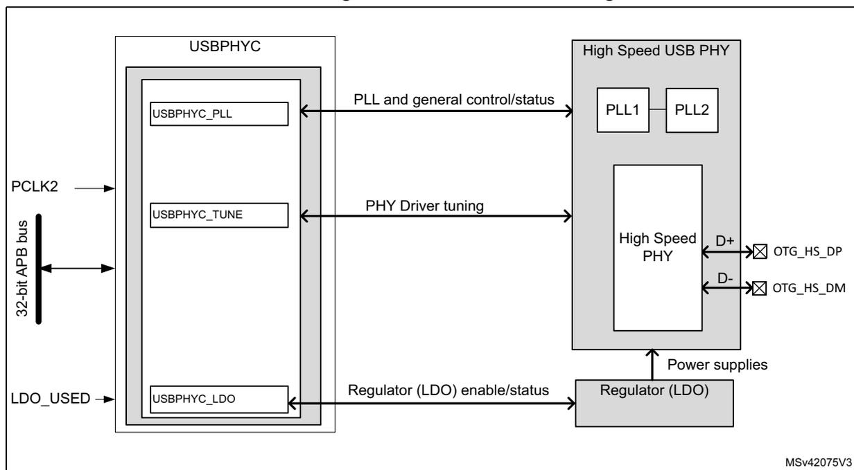
The diagram illustrates the internal architecture of the USBPHYC. On the left, a 32-bit APB bus interface is shown with PCLK2 (clock) and LDO_USED (enable) inputs. The USBPHYC block contains three sub-modules: USBPHYC_PLL, USBPHYC_TUNE, and USBPHYC_LDO. These are connected to the High Speed USB PHY block on the right. USBPHYC_PLL connects to PLL1 and PLL2 via 'PLL and general control/status' lines. USBPHYC_TUNE connects to the High Speed PHY via 'PHY Driver tuning' lines. USBPHYC_LDO connects to a Regulator (LDO) via 'Regulator (LDO) enable/status' lines. The Regulator (LDO) provides 'Power supplies' to the High Speed PHY. The High Speed PHY block contains PLL1, PLL2, and a High Speed PHY core. The High Speed PHY core has two output pins: D+ connected to OTG_HS_DP and D- connected to OTG_HS_DM.
33.3.2 USBPHYC reset and clocks
As an APB peripheral, the only clock used directly in the USBPHYC is the PCLK of the APB bus interface (PCLK2). The APB bus reset resets the registers.
33.4 USBPHYC register interface
33.4.1 USBPHYC PLL1 control register (USBPHYC_PLL1)
Address offset: 0x000
Reset value: 0x0000 0000
This register is used to control the PLL1 of the High Speed PHY.
| 31 | 30 | 29 | 28 | 27 | 26 | 25 | 24 | 23 | 22 | 21 | 20 | 19 | 18 | 17 | 16 |
|---|---|---|---|---|---|---|---|---|---|---|---|---|---|---|---|
| Res. | Res. | Res. | Res. | Res. | Res. | Res. | Res. | Res. | Res. | Res. | Res. | Res. | Res. | Res. | Res. |
| 15 | 14 | 13 | 12 | 11 | 10 | 9 | 8 | 7 | 6 | 5 | 4 | 3 | 2 | 1 | 0 |
| Res. | Res. | Res. | Res. | Res. | Res. | Res. | Res. | Res. | Res. | Res. | Res. | PLLSEL[2:0] | PLLEN | ||
| rw | rw | rw | rw | ||||||||||||
Bits 31:4 Reserved
Bits 3:1 PLL1SEL[2:0] : Controls the PHY PLL1 input clock frequency selection
- 000: 12 MHz
- 001: 12.5 MHz
- 010: 12.5 MHz
- 011: 16 MHz
- 100: 24 MHz
- 101: 25 MHz
- 110: 25 MHz
- 111: reserved
Bit 0 PLL1EN : Enable the PLL1 inside PHY
- 0: PLL1 disabled
- 1: PLL1 enabled
33.4.2 USBPHYC tuning control register (USBPHYC_TUNE)
Address offset: 0x00C
Reset value: 0x0000 0004
This register is used to control the tuning interface of the High Speed PHY.
| 31 | 30 | 29 | 28 | 27 | 26 | 25 | 24 | 23 | 22 | 21 | 20 | 19 | 18 | 17 | 16 |
|---|---|---|---|---|---|---|---|---|---|---|---|---|---|---|---|
| Res. | Res. | Res. | Res. | Res. | Res. | Res. | Res. | SQLBYP | SHTCCTC TLPROT | HSRXOFF[1:0] | HSFALL PREEM | STAGS EL | HFRXG NEQEN | SQLCH CTL[1] | |
| rw | rw | rw | rw | rw | rw | rw | rw | ||||||||
| 15 | 14 | 13 | 12 | 11 | 10 | 9 | 8 | 7 | 6 | 5 | 4 | 3 | 2 | 1 | 0 |
| SQLCH CTL[0] | HSDRVCHKZ TRM[1:0] | HSDRVCHKITRM[3:0] | HSDRV RFRED | FSDRV RFADJ | HSDRVC URINGR | HSDRV DCLEV | HSDRV DCCUR | HSDRVS LEW | LFSCA PEN | INCUR RINT | INCUR REN | ||||
| rw | rw | rw | rw | rw | rw | rw | rw | rw | rw | rw | rw | rw | rw | rw | rw |
Bits 31:4 Reserved
Bit 23 SQLBYP : This pin is used to bypass the squelch inter-locking circuitry
- 0: Do not bypass the squelch inter-locking
- 1: Bypass the squelch inter-locking
Bit 22 SHTCCTCLPROT : Enables the short circuit protection circuitry in LS/FS driver
- 0: short circuit protection disabled
- 1: short circuit protection enabled
Bits 21:20 HSRXOFF[1:0] : HS Receiver Offset adjustment
- 00: off
- 01: + 5mV
- 10: +10 mV
- 11: -5 mV
Bit 19 HSFALLPREEM : HS Fall time control of single ended signals during pre-emphasis:
- 0: control on
- 1: control off
Bit 18 STAGSEL : HS Tx staggering enable:
- 0: Disable the basic staggering in the HS Tx Mode.
- 1: Enable the basic staggering in the HS Tx Mode.
Bit 17 HDRXGNEQEN : Enables the HS Rx Gain Equalizer:
- 0: Disable the Gain Equalizer
- 1: Enable the Gain Equalizer
Bits 16:15 SQLCHCTL[1:0] : Adjust the squelch DC threshold value
- 00: No shift in threshold.
- 01: Squelch DC threshold shift by -5 mv.
- 10: Squelch DC threshold shift by +7 mv.
- 11: Squelch DC threshold shift by +14 mv.
Bits 14:13 HSDRVCHKZTRM[1:0] : Controls the PHY bus HS driver impedance tuning for choke compensation
- 00: No impedance offset
- 01: Reduce the impedance by 2 ohms
- 10: Reduce the impedance by 4 ohms
- 11: Reduce the impedance by 6 ohms
Bits 12:9 HSDRVCHKITRM[3:0] : HS Driver current trimming pins for choke compensation.
- 0000: 18.87 mA target current / nominal + 0%
- 0001: 19.165 mA target current / nominal + 1.56%
- 0010: 19.46 mA target current / nominal + 3.12%
- 0011: 19.755 mA target current / nominal + 4.68%
- 0100: 20.05 mA target current / nominal + 6.24%
- 0101: 20.345 mA target current / nominal + 7.8%
- 0110: 20.64 mA target current / nominal + 9.36%
- 0111: 20.935 mA target current / nominal + 10.92%
- 1000: 21.23 mA target current / nominal + 12.48%
- 1001: 21.525 mA target current / nominal + 14.04%
- 1010: 21.82 mA target current / nominal + 15.6%
- 1011: 22.115 mA target current / nominal + 17.16%
- 1100: 22.458 mA target current / nominal + 19.01%
- 1101: 22.755 mA target current / nominal + 20.58%
- 1110: 23.052 mA target current / nominal + 22.16%
- 1111: 23.348 mA target current / nominal + 23.73%
Bit 8 HSDRVRFRED : High Speed rise-fall reduction enable.
- 0: Default rise/fall time.
- 1: Increases the rise/fall time by 20%.
Bit 7 FSDRVRFADJ : Tuning pin to adjust the full speed rise/fall time.
- 0: Disables the full speed rise/fall tuning option.
- 1: Enables the full speed rise/fall tuning option.
Bit 6 HSDRVCURINCR : Enable the HS driver current increase feature.
- 0: Disables the HSDRVDCEV feature.
- 1: Enables the HSDRVDCEV feature.
Bit 5 HSDRVDCEV : Increases the HS Driver DC level. Not applicable during the HS Test J and Test K data transfer.
- 0: Increases the HS driver DC level by 5 to 7 mV if HSDRVCURINCR = '1'
- 1: Increases the HS driver DC level by 10 to 14 mV if HSDRVCURINCR = '1'
Bit 4 HSDRVDCUR : Decreases the HS driver DC level.
- 0: Keeps the normal HS driver DC level.
- 1: Decreases the HS driver DC level by 5 to 7 mV.
- Bit 3
HSDRV SLEW
: Controls the HS driver slew rate.
- 0: Keeps the normal slew rate.
- 1: Slows the driver slew rate by 10%.
- Bit 2
LFSCAPEN
: Enables the Low Full Speed feedback capacitor.
- 0: Disables the feedback capacitor.
- 1: Enables the feedback capacitor.
- Bit 1
INCURRINT
: Controls PHY current boosting.
- 0: Provides a current boosting of 1mA if INCURREN = '1'.
- 1: Provides a current boosting of 2mA if INCURREN = '1'.
- Bit 0
INCURREN
: Controls the current boosting function.
- 0: Disables the current boosting.
- 1: Enables the current boosting.
33.4.3 USBPHYC LDO control and status register (USBPHYC_LDO)
Address offset: 0x018
Reset value: 0x0000 0001
This register is used to control the register (LDO) associated with the HS USB PHY
| 31 | 30 | 29 | 28 | 27 | 26 | 25 | 24 | 23 | 22 | 21 | 20 | 19 | 18 | 17 | 16 |
|---|---|---|---|---|---|---|---|---|---|---|---|---|---|---|---|
| Res. | Res. | Res. | Res. | Res. | Res. | Res. | Res. | Res. | Res. | Res. | Res. | Res. | Res. | Res. | Res. |
| 15 | 14 | 13 | 12 | 11 | 10 | 9 | 8 | 7 | 6 | 5 | 4 | 3 | 2 | 1 | 0 |
| Res. | Res. | Res. | Res. | Res. | Res. | Res. | Res. | Res. | Res. | Res. | Res. | Res. | LDO_DISABLE | LDO_STATUS | LDO_USED |
| rw | r | r |
Bits 31:3 Reserved
- Bit 2
LDO_DISABLE
: Controls disable of the High Speed PHY's LDO.
- 0: LDO enabled
- 1: LDO disabled
- Bit 1
LDO_STATUS
: Monitors the status of the PHY's LDO.
- 0: LDO not ready
- 1: LDO ready
- Bit 0
LDO_USED
: Indicates the presence of the LDO in the chip.
- 0: LDO is not used
- 1: LDO is used
33.4.4 USBPHYC register map
Table 239. USBPHYC register map and reset values
| Offset | Register | 31 | 30 | 29 | 28 | 27 | 26 | 25 | 24 | 23 | 22 | 21 | 20 | 19 | 18 | 17 | 16 | 15 | 14 | 13 | 12 | 11 | 10 | 9 | 8 | 7 | 6 | 5 | 4 | 3 | 2 | 1 | 0 |
|---|---|---|---|---|---|---|---|---|---|---|---|---|---|---|---|---|---|---|---|---|---|---|---|---|---|---|---|---|---|---|---|---|---|
| 0x00 | USBPHYC_PLL1 | Res | Res | Res | Res | Res | Res | Res | Res | Res | Res | Res | Res | Res | Res | Res | Res | Res | Res | Res | Res | Res | Res | Res | Res | Res | Res | Res | Res | Res | Res | PLL1SEL[2:0] | PLL1EN |
| Reset value | 0 | 0 | 0 | ||||||||||||||||||||||||||||||
| .0x010-0x008 | Reserved | ||||||||||||||||||||||||||||||||
| 0x00C | USBPHYC_TUNE | Res | Res | Res | Res | Res | Res | Res | Res | SQLBYP | SHTCCTCLPROT | HSRXOFF[1:0] | HSFALLPREEM | STAGSEL | HFRXGNEQEN | SQLCHCTL[1:0] | HSDRVCHKZTRM[1:0] | HSDRVCHKZTRM[3:0] | Res | Res | Res | Res | Res | Res | HSDRVRFRED | FSDRVRFADJ | HSDRVCURINGR | HSDRVDCLEV | HSDRVDCCUR | HSDRVISLEW | LFSCAPEN | INCURRINT | INCURREN |
| Reset value | 0 | 0 | 0 | 0 | 0 | 0 | 0 | 0 | 0 | 0 | 0 | 0 | 0 | 0 | 0 | 0 | 0 | 0 | 0 | 0 | 0 | 1 | 0 | 0 | |||||||||
| .0x010-0x014 | Reserved | ||||||||||||||||||||||||||||||||
| 0x018 | USBPHYC_LDO | Res | Res | Res | Res | Res | Res | Res | Res | Res | Res | Res | Res | Res | Res | Res | Res | Res | Res | Res | Res | Res | Res | Res | Res | Res | Res | Res | Res | Res | LDO_DISABLE | LDO_STATUS | LDO_USED |
| Reset value | 0 | 0 | 1 | ||||||||||||||||||||||||||||||
Refer to Section 1.6 on page 56 for the register boundary addresses.