21. Basic timers (TIM6/TIM7)
21.1 TIM6/TIM7 introduction
The basic timers TIM6 and TIM7 consist of a 16-bit auto-reload counter driven by a programmable prescaler.
They may be used as generic timers for time base generation but they are also specifically used to drive the digital-to-analog converter (DAC). In fact, the timers are internally connected to the DAC and are able to drive it through their trigger outputs.
The timers are completely independent, and do not share any resources.
21.2 TIM6/TIM7 main features
Basic timer (TIM6/TIM7) features include:
- • 16-bit auto-reload upcounter
- • 16-bit programmable prescaler used to divide (also “on the fly”) the counter clock frequency by any factor between 1 and 65535
- • Synchronization circuit to trigger the DAC
- • Interrupt/DMA generation on the update event: counter overflow
Figure 267. Basic timer block diagram
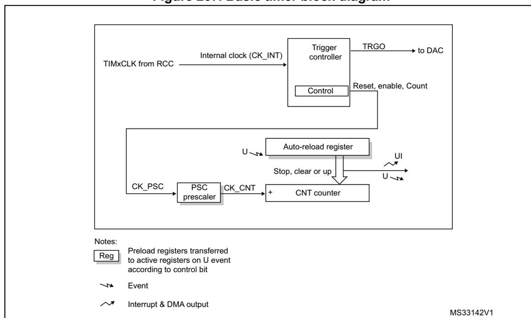
The block diagram illustrates the internal architecture of a basic timer (TIM6/TIM7). The main components are:
- Internal clock (CK_INT): Derived from TIMxCLK from RCC, it is fed into the Trigger controller.
- Trigger controller: Receives CK_INT and control signals (Reset, enable, Count). It generates the TRGO output to the DAC.
- Control: A sub-block within the Trigger controller that receives input from the Auto-reload register and CNT counter.
- CK_PSC: Input to the PSC prescaler.
- PSC prescaler: Divides the CK_PSC signal to produce CK_CNT.
- CNT counter: Receives CK_CNT and control signals. It generates the U (Update) and UI (Interrupt & DMA output) signals.
- Auto-reload register: Receives input from the CNT counter and provides control signals to the Trigger controller and PSC prescaler. It also generates the U (Update) signal.
Notes:
- Reg (Preload registers transferred to active registers on U event according to control bit)
- Event (U signal)
- Interrupt & DMA output (UI signal)
MS33142V1
21.3 TIM6/TIM7 functional description
21.3.1 Time-base unit
The main block of the programmable timer is a 16-bit upcounter with its related auto-reload register. The counter clock can be divided by a prescaler.
The counter, the auto-reload register and the prescaler register can be written or read by software. This is true even when the counter is running.
The time-base unit includes:
- • Counter Register (TIMx_CNT)
- • Prescaler Register (TIMx_PSC)
- • Auto-Reload Register (TIMx_ARR)
The auto-reload register is preloaded. The preload register is accessed each time an attempt is made to write or read the auto-reload register. The contents of the preload register are transferred into the shadow register permanently or at each update event UEV, depending on the auto-reload preload enable bit (ARPE) in the TIMx_CR1 register. The update event is sent when the counter reaches the overflow value and if the UDIS bit equals 0 in the TIMx_CR1 register. It can also be generated by software. The generation of the update event is described in detail for each configuration.
The counter is clocked by the prescaler output CK_CNT, which is enabled only when the counter enable bit (CEN) in the TIMx_CR1 register is set.
Note that the actual counter enable signal CNT_EN is set 1 clock cycle after CEN.
Prescaler description
The prescaler can divide the counter clock frequency by any factor between 1 and 65536. It is based on a 16-bit counter controlled through a 16-bit register (in the TIMx_PSC register). It can be changed on the fly as the TIMx_PSC control register is buffered. The new prescaler ratio is taken into account at the next update event.
Figure 268 and Figure 269 give some examples of the counter behavior when the prescaler ratio is changed on the fly.
Figure 268. Counter timing diagram with prescaler division change from 1 to 2
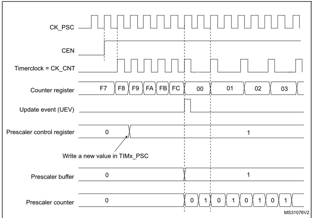
This timing diagram shows the relationship between several signals over time. The signals are:
- CK_PSC : A periodic clock signal.
- CEN : Counter Enable signal, which goes high to start counting.
- Timerclock = CK_CNT : The clock for the counter, derived from CK_PSC.
- Counter register : Shows hexadecimal values F7, F8, F9, FA, FB, FC, followed by 00, 01, 02, 03.
- Update event (UEV) : A pulse generated when the counter overflows.
- Prescaler control register : Shows a value of 0 initially, then changes to 1. An arrow points to the transition with the text "Write a new value in TIMx_PSC".
- Prescaler buffer : Shows a value of 0 initially, then changes to 1 at the time of the update event.
- Prescaler counter : Shows a sequence of values 0, 1, 0, 1, 0, 1, 0, 1, indicating a division of 2 after the update.
Figure 269. Counter timing diagram with prescaler division change from 1 to 4
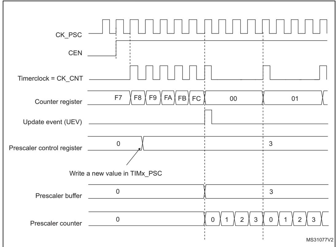
This timing diagram is similar to Figure 268 but shows a prescaler division change from 1 to 4. The signals are:
- CK_PSC : Clock signal.
- CEN : Counter Enable signal.
- Timerclock = CK_CNT : Counter clock signal.
- Counter register : Shows values F7, F8, F9, FA, FB, FC, 00, 01.
- Update event (UEV) : Update pulse.
- Prescaler control register : Changes from 0 to 3. An arrow points to the transition with the text "Write a new value in TIMx_PSC".
- Prescaler buffer : Changes from 0 to 3 at the update event.
- Prescaler counter : Shows a sequence of values 0, 1, 2, 3, 0, 1, 2, 3, indicating a division of 4 after the update.
21.3.2 Counting mode
The counter counts from 0 to the auto-reload value (contents of the TIMx_ARR register), then restarts from 0 and generates a counter overflow event.
An update event can be generated at each counter overflow or by setting the UG bit in the TIMx_EGR register (by software or by using the slave mode controller).
The UEV event can be disabled by software by setting the UDIS bit in the TIMx_CR1 register. This avoids updating the shadow registers while writing new values into the preload registers. In this way, no update event occurs until the UDIS bit has been cleared, however, the counter and the prescaler counter both restart from 0 (but the prescale rate does not change). In addition, if the URS (update request selection) bit in the TIMx_CR1 register is set, setting the UG bit generates an update event UEV, but the UIF flag is not set (so no interrupt or DMA request is sent).
When an update event occurs, all the registers are updated and the update flag (UIF bit in the TIMx_SR register) is set (depending on the URS bit):
- • The buffer of the prescaler is reloaded with the preload value (contents of the TIMx_PSC register)
- • The auto-reload shadow register is updated with the preload value (TIMx_ARR)
The following figures show some examples of the counter behavior for different clock frequencies when TIMx_ARR = 0x36.
Figure 270. Counter timing diagram, internal clock divided by 1
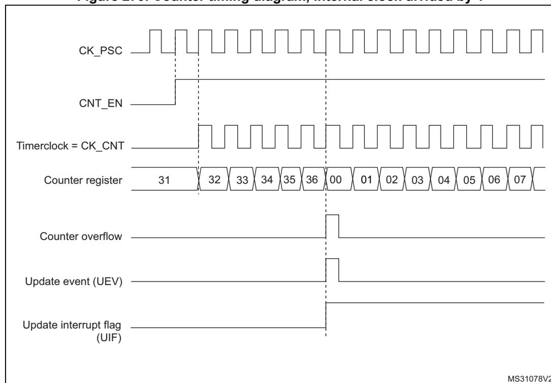
The timing diagram illustrates the operation of a counter in counting mode. The signals shown are:
- CK_PSC : Prescaler clock signal, shown as a square wave.
- CNT_EN : Counter enable signal, which is a high-level signal that enables the counter.
- Timerclock = CK_CNT : Counter clock signal, which is a square wave derived from CK_PSC.
- Counter register : A sequence of values starting at 31, then 32, 33, 34, 35, 36, 00, 01, 02, 03, 04, 05, 06, 07, indicating a count from 0 to 36 (0x24) and then rolling over to 0.
- Counter overflow : A pulse generated when the counter reaches the auto-reload value (36) and rolls over to 0.
- Update event (UEV) : A pulse generated when the counter overflows or when the UG bit is set in the TIMx_EGR register.
- Update interrupt flag (UIF) : A pulse generated when the counter overflows or when the UG bit is set in the TIMx_EGR register.
The diagram shows that the counter counts from 0 to 36 (0x24) and then rolls over to 0. The counter overflow, update event (UEV), and update interrupt flag (UIF) are all generated when the counter reaches the auto-reload value (36) and rolls over to 0. The counter register values are shown in a sequence: 31, 32, 33, 34, 35, 36, 00, 01, 02, 03, 04, 05, 06, 07.
MS31078V2
Figure 271. Counter timing diagram, internal clock divided by 2
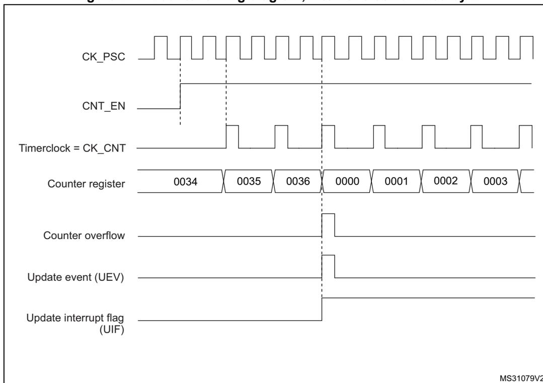
Timing diagram showing the relationship between the prescaler clock (CK_PSC), counter enable (CNT_EN), timer clock (CK_CNT), counter register values, counter overflow, update event (UEV), and update interrupt flag (UIF) when the internal clock is divided by 2.
The diagram illustrates the following signals and events:
- CK_PSC : Prescaler clock signal (square wave).
- CNT_EN : Counter enable signal (high level).
- Timerclock = CK_CNT : Counter clock signal (square wave, half the frequency of CK_PSC).
- Counter register : Shows the sequence of values: 0034, 0035, 0036, 0000, 0001, 0002, 0003.
- Counter overflow : Pulse generated when the counter reaches 0036 and rolls over to 0000.
- Update event (UEV) : Pulse generated when the counter rolls over.
- Update interrupt flag (UIF) : Flag set when the counter rolls over.
MS31079V2
Figure 272. Counter timing diagram, internal clock divided by 4
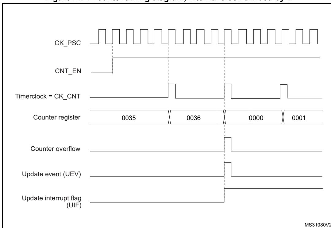
Timing diagram showing the relationship between the prescaler clock (CK_PSC), counter enable (CNT_EN), timer clock (CK_CNT), counter register values, counter overflow, update event (UEV), and update interrupt flag (UIF) when the internal clock is divided by 4.
The diagram illustrates the following signals and events:
- CK_PSC : Prescaler clock signal (square wave).
- CNT_EN : Counter enable signal (high level).
- Timerclock = CK_CNT : Counter clock signal (square wave, one-quarter the frequency of CK_PSC).
- Counter register : Shows the sequence of values: 0035, 0036, 0000, 0001.
- Counter overflow : Pulse generated when the counter reaches 0036 and rolls over to 0000.
- Update event (UEV) : Pulse generated when the counter rolls over.
- Update interrupt flag (UIF) : Flag set when the counter rolls over.
MS31080V2
Figure 273. Counter timing diagram, internal clock divided by N
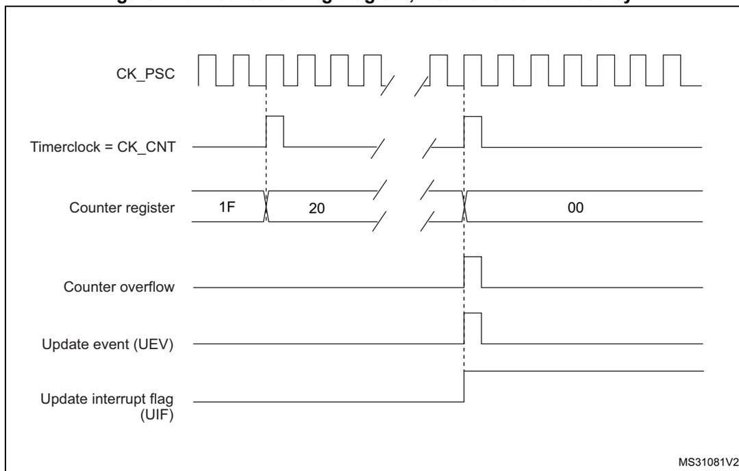
Timing diagram showing the relationship between the prescaler clock (CK_PSC), timer clock (CK_CNT), counter register, counter overflow, update event (UEV), and update interrupt flag (UIF) when the internal clock is divided by N.
- CK_PSC: Prescaler clock signal, shown as a continuous square wave.
- Timerclock = CK_CNT: Timer clock signal, derived from CK_PSC. It shows pulses corresponding to the counter increments.
- Counter register: Shows the counter value. It is at 1F, increments to 20, and then resets to 00 after an overflow.
- Counter overflow: A high pulse generated when the counter register reaches its limit and resets to 00.
- Update event (UEV): A high pulse synchronized with the counter overflow.
- Update interrupt flag (UIF): A signal that transitions from low to high at the update event.
MS31081V2
Figure 274. Counter timing diagram, update event when ARPE = 0 (TIMx_ARR not preloaded)
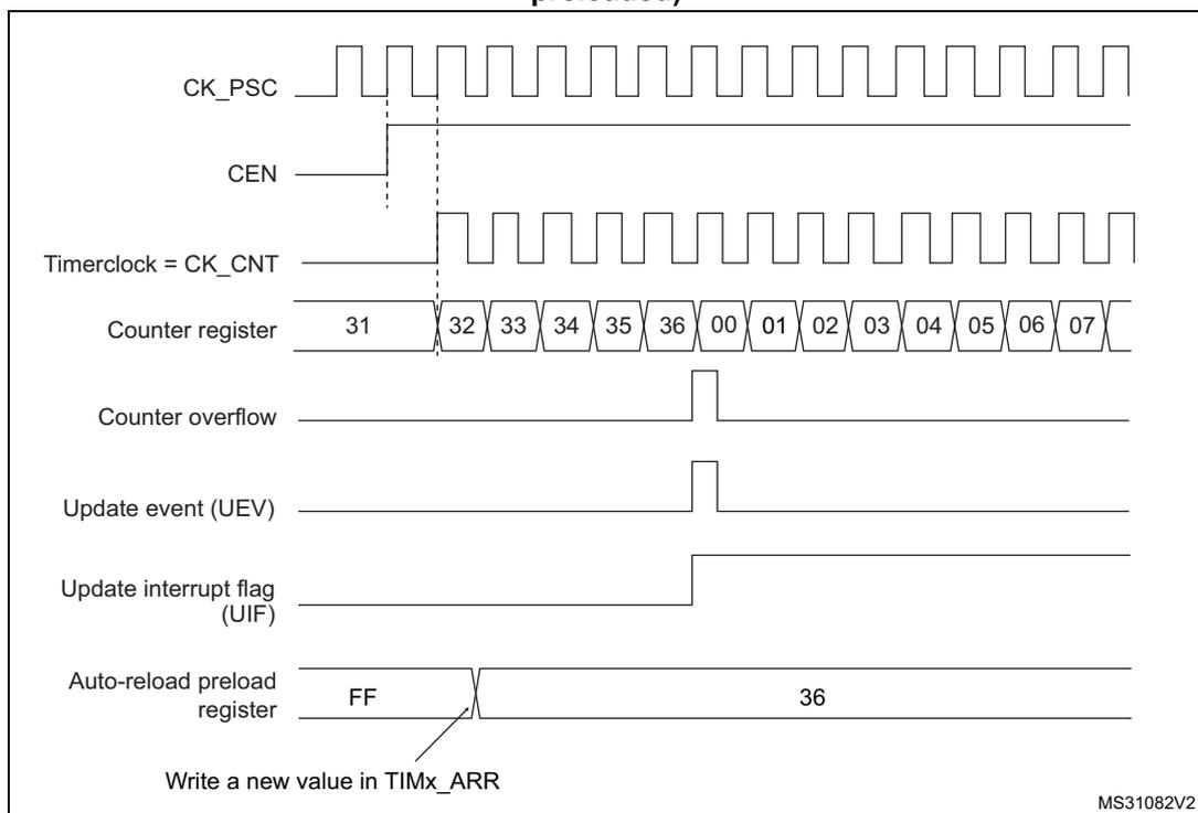
Timing diagram showing the relationship between the prescaler clock (CK_PSC), counter enable (CEN), timer clock (CK_CNT), counter register, counter overflow, update event (UEV), update interrupt flag (UIF), and auto-reload preload register when ARPE = 0 and TIMx_ARR is not preloaded.
- CK_PSC: Prescaler clock signal, shown as a continuous square wave.
- CEN: Counter enable signal, which goes high to start the timer.
- Timerclock = CK_CNT: Timer clock signal, active when CEN is high.
- Counter register: Shows the counter value incrementing: 31, 32, 33, 34, 35, 36, then resetting to 00 and continuing 01, 02, 03, 04, 05, 06, 07.
- Counter overflow: A high pulse generated when the counter register reaches 36 (the new ARR value) and resets to 00.
- Update event (UEV): A high pulse synchronized with the counter overflow.
- Update interrupt flag (UIF): A signal that transitions from low to high at the update event.
- Auto-reload preload register: Shows the value changing from FF to 36. An arrow indicates the "Write a new value in TIMx_ARR" event which occurs while the counter is running.
MS31082V2
Figure 275. Counter timing diagram, update event when ARPE=1 (TIMx_ARR preloaded)
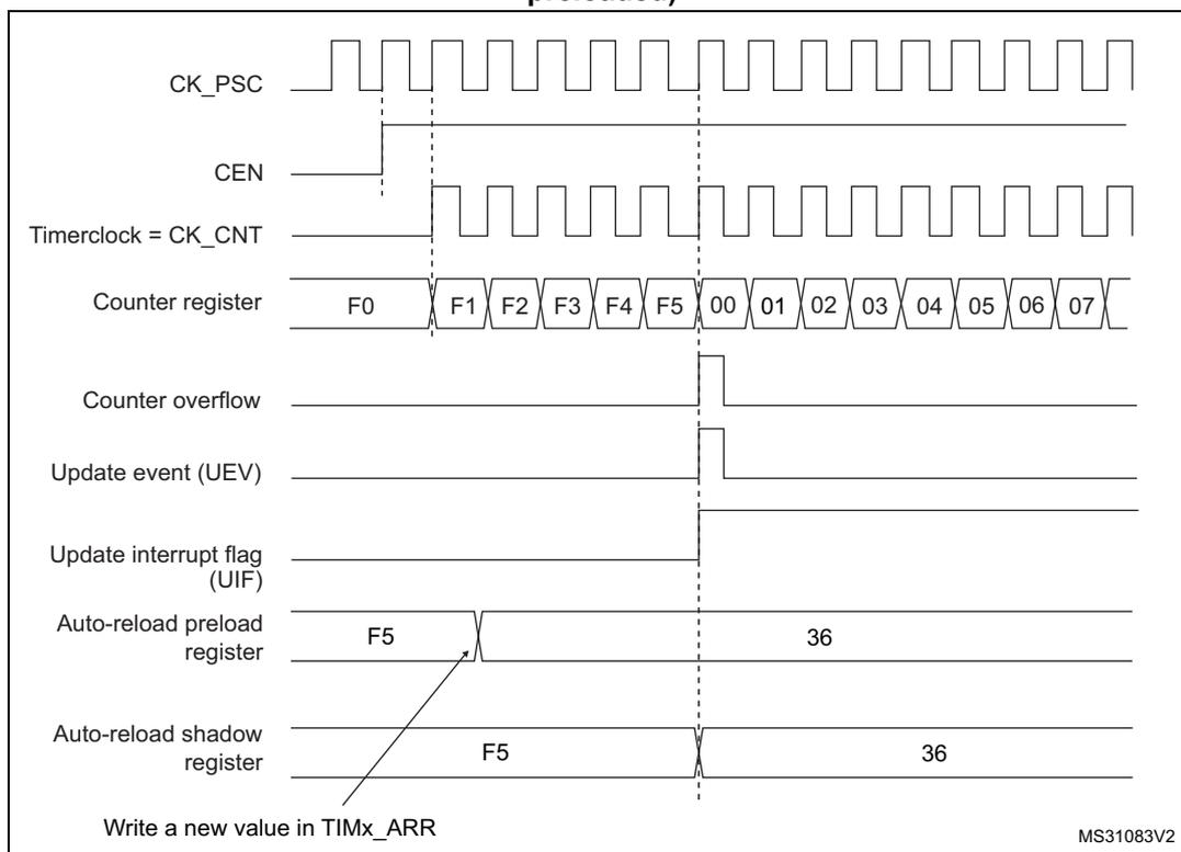
The diagram illustrates the timing of a basic timer (TIM6/TIM7) in update mode with ARPE=1. The signals shown are:
- CK_PSC : Prescaler clock signal, shown as a square wave.
- CEN : Counter Enable signal, which is high to enable counting.
- Timerclock = CK_CNT : Counter clock signal, derived from CK_PSC.
- Counter register : Shows the counter values: F0, F1, F2, F3, F4, F5, 00, 01, 02, 03, 04, 05, 06, 07. The counter increments on each rising edge of CK_CNT.
- Counter overflow : A pulse is generated when the counter rolls over from F5 to 00.
- Update event (UEV) : A pulse is generated when the counter reaches F5.
- Update interrupt flag (UIF) : A pulse is generated when the counter reaches F5.
- Auto-reload preload register : Shows the value F5 being updated to 36 when the counter reaches F5.
- Auto-reload shadow register : Shows the value F5 being updated to 36 when the counter reaches F5.
A note at the bottom left indicates: "Write a new value in TIMx_ARR". The diagram is labeled MS31083V2.
21.3.3 UIF bit remapping
The IUFREMAP bit in the TIMx_CR1 register forces a continuous copy of the Update Interrupt Flag UIF into the timer counter register's bit 31 (TIMxCNT[31]). This allows to atomically read both the counter value and a potential roll-over condition signaled by the UIFCPY flag. In particular cases, it can ease the calculations by avoiding race conditions caused for instance by a processing shared between a background task (counter reading) and an interrupt (Update Interrupt).
There is no latency between the assertions of the UIF and UIFCPY flags.
21.3.4 Clock source
The counter clock is provided by the Internal clock (CK_INT) source.
The CEN (in the TIMx_CR1 register) and UG bits (in the TIMx_EGR register) are actual control bits and can be changed only by software (except for UG that remains cleared automatically). As soon as the CEN bit is written to 1, the prescaler is clocked by the internal clock CK_INT.
Figure 276 shows the behavior of the control circuit and the upcounter in normal mode, without prescaler.
Figure 276. Control circuit in normal mode, internal clock divided by 1
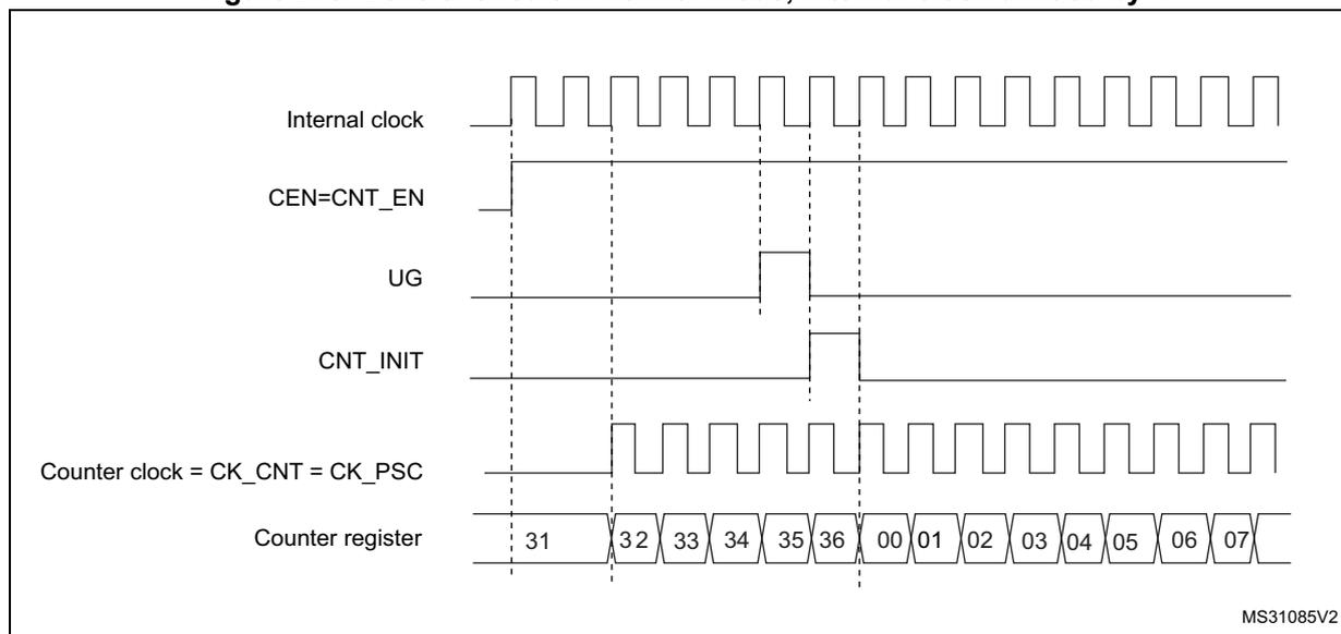
MS31085V2
21.3.5 Debug mode
When the microcontroller enters the debug mode (Cortex®-M7 core - halted), the TIMx counter either continues to work normally or stops, depending on the DBG_TIMx_STOP configuration bit in the DBG module. For more details, refer to Section 34.16.2: Debug support for timers, watchdog, bxCAN and I 2 C .
21.4 TIM6/TIM7 registers
Refer to Section 1.2 on page 54 for a list of abbreviations used in register descriptions.
The peripheral registers can be accessed by half-words (16-bit) or words (32-bit).
21.4.1 TIMx control register 1 (TIMx_CR1)(x = 6 to 7)
Address offset: 0x00
Reset value: 0x0000
| 15 | 14 | 13 | 12 | 11 | 10 | 9 | 8 | 7 | 6 | 5 | 4 | 3 | 2 | 1 | 0 |
|---|---|---|---|---|---|---|---|---|---|---|---|---|---|---|---|
| Res. | Res. | Res. | Res. | UIFREMAP | Res. | Res. | Res. | ARPE | Res. | Res. | Res. | OPM | URS | UDIS | CEN |
| rw | rw | rw | rw | rw | rw |
Bits 15:12 Reserved, must be kept at reset value.
Bit 11 UIFREMAP : UIF status bit remapping
0: No remapping. UIF status bit is not copied to TIMx_CNT register bit 31.
1: Remapping enabled. UIF status bit is copied to TIMx_CNT register bit 31.
Bits 10:8 Reserved, must be kept at reset value.
Bit 7 ARPE : Auto-reload preload enable
0: TIMx_ARR register is not buffered.
1: TIMx_ARR register is buffered.
Bits 6:4 Reserved, must be kept at reset value.
Bit 3 OPM : One-pulse mode
0: Counter is not stopped at update event
1: Counter stops counting at the next update event (clearing the CEN bit).
Bit 2 URS : Update request source
This bit is set and cleared by software to select the UEV event sources.
0: Any of the following events generates an update interrupt or DMA request if enabled.
These events can be:
- – Counter overflow/underflow
- – Setting the UG bit
- – Update generation through the slave mode controller
1: Only counter overflow/underflow generates an update interrupt or DMA request if enabled.
Bit 1 UDIS : Update disable
This bit is set and cleared by software to enable/disable UEV event generation.
0: UEV enabled. The Update (UEV) event is generated by one of the following events:
- – Counter overflow/underflow
- – Setting the UG bit
- – Update generation through the slave mode controller
Buffered registers are then loaded with their preload values.
1: UEV disabled. The Update event is not generated, shadow registers keep their value (ARR, PSC). However the counter and the prescaler are reinitialized if the UG bit is set or if a hardware reset is received from the slave mode controller.
Bit 0 CEN : Counter enable
0: Counter disabled
1: Counter enabled
Note: Gated mode can work only if the CEN bit has been previously set by software.
However trigger mode can set the CEN bit automatically by hardware.
CEN is cleared automatically in one-pulse mode, when an update event occurs.
21.4.2 TIMx control register 2 (TIMx_CR2)(x = 6 to 7)
Address offset: 0x04
Reset value: 0x0000
| 15 | 14 | 13 | 12 | 11 | 10 | 9 | 8 | 7 | 6 | 5 | 4 | 3 | 2 | 1 | 0 |
|---|---|---|---|---|---|---|---|---|---|---|---|---|---|---|---|
| Res. | Res. | Res. | Res. | Res. | Res. | Res. | Res. | Res. | MMS[2:0] | Res. | Res. | Res. | Res. | ||
| rw | rw | rw | |||||||||||||
Bits 15:7 Reserved, must be kept at reset value.
Bits 6:4 MMS[2:0] : Master mode selection
These bits are used to select the information to be sent in master mode to slave timers for synchronization (TRGO). The combination is as follows:
000: Reset - the UG bit from the TIMx_EGR register is used as a trigger output (TRGO). If reset is generated by the trigger input (slave mode controller configured in reset mode) then the signal on TRGO is delayed compared to the actual reset.
001: Enable - the Counter enable signal, CNT_EN, is used as a trigger output (TRGO). It is useful to start several timers at the same time or to control a window in which a slave timer is enabled. The Counter Enable signal is generated by a logic OR between CEN control bit and the trigger input when configured in gated mode.
When the Counter Enable signal is controlled by the trigger input, there is a delay on TRGO, except if the master/slave mode is selected (see the MSM bit description in the TIMx_SMCR register).
010: Update - The update event is selected as a trigger output (TRGO). For instance a master timer can then be used as a prescaler for a slave timer.
Note: The clock of the slave timer or ADC must be enabled prior to receive events from the master timer, and must not be changed on-the-fly while triggers are received from the master timer.
Bits 3:0 Reserved, must be kept at reset value.
21.4.3 TIMx DMA/Interrupt enable register (TIMx_DIER)(x = 6 to 7)
Address offset: 0x0C
Reset value: 0x0000
| 15 | 14 | 13 | 12 | 11 | 10 | 9 | 8 | 7 | 6 | 5 | 4 | 3 | 2 | 1 | 0 |
|---|---|---|---|---|---|---|---|---|---|---|---|---|---|---|---|
| Res. | Res. | Res. | Res. | Res. | Res. | Res. | UDE | Res. | Res. | Res. | Res. | Res. | Res. | Res. | UIE |
| rw | rw |
Bits 15:9 Reserved, must be kept at reset value.
Bit 8 UDE : Update DMA request enable
0: Update DMA request disabled.
1: Update DMA request enabled.
Bits 7:1 Reserved, must be kept at reset value.
Bit 0 UIE : Update interrupt enable
0: Update interrupt disabled.
1: Update interrupt enabled.
21.4.4 TIMx status register (TIMx_SR)(x = 6 to 7)
Address offset: 0x10
Reset value: 0x0000
| 15 | 14 | 13 | 12 | 11 | 10 | 9 | 8 | 7 | 6 | 5 | 4 | 3 | 2 | 1 | 0 |
|---|---|---|---|---|---|---|---|---|---|---|---|---|---|---|---|
| Res. | Res. | Res. | Res. | Res. | Res. | Res. | Res. | Res. | Res. | Res. | Res. | Res. | Res. | Res. | UIF |
| rc_w0 |
Bits 15:1 Reserved, must be kept at reset value.
Bit 0 UIF : Update interrupt flag
This bit is set by hardware on an update event. It is cleared by software.
0: No update occurred.
1: Update interrupt pending. This bit is set by hardware when the registers are updated:
- – At overflow or underflow regarding the repetition counter value and if UDIS = 0 in the TIMx_CR1 register.
- – When CNT is reinitialized by software using the UG bit in the TIMx_EGR register, if URS = 0 and UDIS = 0 in the TIMx_CR1 register.
21.4.5 TIMx event generation register (TIMx_EGR)(x = 6 to 7)
Address offset: 0x14
Reset value: 0x0000
| 15 | 14 | 13 | 12 | 11 | 10 | 9 | 8 | 7 | 6 | 5 | 4 | 3 | 2 | 1 | 0 |
|---|---|---|---|---|---|---|---|---|---|---|---|---|---|---|---|
| Res. | Res. | Res. | Res. | Res. | Res. | Res. | Res. | Res. | Res. | Res. | Res. | Res. | Res. | Res. | UG |
| w |
Bits 15:1 Reserved, must be kept at reset value.
Bit 0 UG : Update generation
This bit can be set by software, it is automatically cleared by hardware.
0: No action.
1: Re-initializes the timer counter and generates an update of the registers. Note that the prescaler counter is cleared too (but the prescaler ratio is not affected).
21.4.6 TIMx counter (TIMx_CNT)(x = 6 to 7)
Address offset: 0x24
Reset value: 0x0000 0000
| 31 | 30 | 29 | 28 | 27 | 26 | 25 | 24 | 23 | 22 | 21 | 20 | 19 | 18 | 17 | 16 |
|---|---|---|---|---|---|---|---|---|---|---|---|---|---|---|---|
| UIF CPY | Res. | Res. | Res. | Res. | Res. | Res. | Res. | Res. | Res. | Res. | Res. | Res. | Res. | Res. | Res. |
| r |
| 15 | 14 | 13 | 12 | 11 | 10 | 9 | 8 | 7 | 6 | 5 | 4 | 3 | 2 | 1 | 0 |
|---|---|---|---|---|---|---|---|---|---|---|---|---|---|---|---|
| CNT[15:0] | |||||||||||||||
| rw | rw | rw | rw | rw | rw | rw | rw | rw | rw | rw | rw | rw | rw | rw | rw |
Bit 31 UIFCPY : UIF Copy
This bit is a read-only copy of the UIF bit of the TIMx_ISR register. If the UIFREMAP bit in TIMx_CR1 is reset, bit 31 is reserved and read as 0.
Bits 30:16 Reserved, must be kept at reset value.
Bits 15:0 CNT[15:0] : Counter value
21.4.7 TIMx prescaler (TIMx_PSC)(x = 6 to 7)
Address offset: 0x28
Reset value: 0x0000

| 15 | 14 | 13 | 12 | 11 | 10 | 9 | 8 | 7 | 6 | 5 | 4 | 3 | 2 | 1 | 0 |
|---|---|---|---|---|---|---|---|---|---|---|---|---|---|---|---|
| PSC[15:0] | |||||||||||||||
| rw | rw | rw | rw | rw | rw | rw | rw | rw | rw | rw | rw | rw | rw | rw | rw |
Bits 15:0 PSC[15:0] : Prescaler value
The counter clock frequency \( CK\_CNT \) is equal to \( f_{CK\_PSC} / (PSC[15:0] + 1) \) .
PSC contains the value to be loaded into the active prescaler register at each update event. (including when the counter is cleared through UG bit of TIMx_EGR register or through trigger controller when configured in “reset mode”).
21.4.8 TIMx auto-reload register (TIMx_ARR)(x = 6 to 7)
Address offset: 0x2C
Reset value: 0xFFFF

| 15 | 14 | 13 | 12 | 11 | 10 | 9 | 8 | 7 | 6 | 5 | 4 | 3 | 2 | 1 | 0 |
|---|---|---|---|---|---|---|---|---|---|---|---|---|---|---|---|
| ARR[15:0] | |||||||||||||||
| rw | rw | rw | rw | rw | rw | rw | rw | rw | rw | rw | rw | rw | rw | rw | rw |
Bits 15:0 ARR[15:0] : Prescaler value
ARR is the value to be loaded into the actual auto-reload register.
Refer to Section 21.3.1: Time-base unit on page 731 for more details about ARR update and behavior.
The counter is blocked while the auto-reload value is null.
21.4.9 TIMx register map
TIMx registers are mapped as 16-bit addressable registers as described in the table below:
Table 128. TIMx register map and reset values
| Offset | Register name | 31 | 30 | 29 | 28 | 27 | 26 | 25 | 24 | 23 | 22 | 21 | 20 | 19 | 18 | 17 | 16 | 15 | 14 | 13 | 12 | 11 | 10 | 9 | 8 | 7 | 6 | 5 | 4 | 3 | 2 | 1 | 0 |
|---|---|---|---|---|---|---|---|---|---|---|---|---|---|---|---|---|---|---|---|---|---|---|---|---|---|---|---|---|---|---|---|---|---|
| 0x00 | TIMx_CR1 | Res. | Res. | Res. | Res. | Res. | Res. | Res. | Res. | Res. | Res. | Res. | Res. | Res. | Res. | Res. | Res. | Res. | Res. | Res. | Res. | UIFREMA | Res. | Res. | Res. | ARPE | Res. | Res. | Res. | OPM | URS | UDIS | CEN |
| Reset value | 0 | 0 | 0 | 0 | 0 | 0 | |||||||||||||||||||||||||||
| 0x04 | TIMx_CR2 | Res. | Res. | Res. | Res. | Res. | Res. | Res. | Res. | Res. | Res. | Res. | Res. | Res. | Res. | Res. | Res. | Res. | Res. | Res. | Res. | Res. | Res. | Res. | Res. | Res. | MMS [2:0] | Res. | Res. | Res. | Res. | ||
| Reset value | 0 | 0 | 0 | ||||||||||||||||||||||||||||||
| 0x08 | Reserved | ||||||||||||||||||||||||||||||||
| 0x0C | TIMx_DIER | Res. | Res. | Res. | Res. | Res. | Res. | Res. | Res. | Res. | Res. | Res. | Res. | Res. | Res. | Res. | Res. | Res. | Res. | Res. | Res. | Res. | Res. | Res. | UDE | Res. | Res. | Res. | Res. | Res. | Res. | Res. | UIE |
| Reset value | 0 | 0 | |||||||||||||||||||||||||||||||
| 0x10 | TIMx_SR | Res. | Res. | Res. | Res. | Res. | Res. | Res. | Res. | Res. | Res. | Res. | Res. | Res. | Res. | Res. | Res. | Res. | Res. | Res. | Res. | Res. | Res. | Res. | Res. | Res. | Res. | Res. | Res. | Res. | Res. | Res. | UIF |
| Reset value | 0 | ||||||||||||||||||||||||||||||||
| 0x14 | TIMx_EGR | Res. | Res. | Res. | Res. | Res. | Res. | Res. | Res. | Res. | Res. | Res. | Res. | Res. | Res. | Res. | Res. | Res. | Res. | Res. | Res. | Res. | Res. | Res. | Res. | Res. | Res. | Res. | Res. | Res. | Res. | Res. | UG |
| Reset value | 0 | ||||||||||||||||||||||||||||||||
| 0x18-0x20 | Reserved | ||||||||||||||||||||||||||||||||
| 0x24 | TIMx_CNT | UIFCOPY or Res. | Res. | Res. | Res. | Res. | Res. | Res. | Res. | Res. | Res. | Res. | Res. | Res. | Res. | Res. | Res. | Res. | Res. | Res. | Res. | Res. | Res. | Res. | Res. | Res. | Res. | Res. | Res. | Res. | Res. | Res. | CNT[15:0] |
| Reset value | 0 | 0 | |||||||||||||||||||||||||||||||
| 0x28 | TIMx_PSC | Res. | Res. | Res. | Res. | Res. | Res. | Res. | Res. | Res. | Res. | Res. | Res. | Res. | Res. | Res. | Res. | Res. | Res. | Res. | Res. | Res. | Res. | Res. | Res. | Res. | Res. | Res. | Res. | Res. | Res. | Res. | PSC[15:0] |
| Reset value | 0 | ||||||||||||||||||||||||||||||||
| 0x2C | TIMx_ARR | Res. | Res. | Res. | Res. | Res. | Res. | Res. | Res. | Res. | Res. | Res. | Res. | Res. | Res. | Res. | Res. | Res. | Res. | Res. | Res. | Res. | Res. | Res. | Res. | Res. | Res. | Res. | Res. | Res. | Res. | Res. | ARR[15:0] |
| Reset value | 1 | ||||||||||||||||||||||||||||||||
Refer to Section 1.6 on page 56 for the register boundary addresses.