2. System and memory overview
2.1 System architecture
The main system architecture is based on 2 sub-systems:
- • An AXI to multi AHB bridge converting AXI4 protocol to AHB-Lite protocol:
- – 1x AXI to 64-bit AHB bridge connected to the embedded flash
- – 3x AXI to 32bit AHB bridge connected to AHB bus matrix
- • A multi-AHB Bus-Matrix
Figure 2. System architecture for STM32F72xxx and STM32F73xxx devices
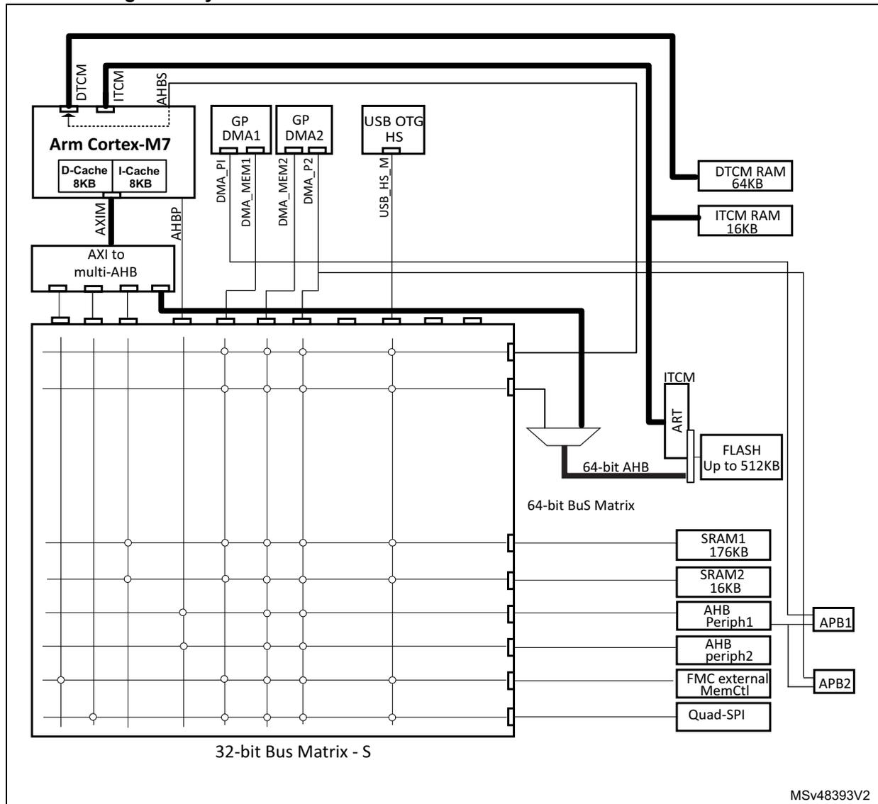
The diagram illustrates the system architecture for STM32F72xxx and STM32F73xxx devices. At the top left is the Arm Cortex-M7 core, which includes D-Cache 8KB and I-Cache 8KB . It is connected to an AXI to multi-AHB bridge via AXIM and AHBP interfaces. The core also has DTCM and ITCM memory interfaces. The AXI to multi-AHB bridge connects to a 64-bit Bus Matrix and a 32-bit Bus Matrix - S . The 64-bit Bus Matrix is connected to GP DMA1 (via DMA_P1 and DMA_MEM1 ), GP DMA2 (via DMA_P2 and DMA_MEM2 ), and USB OTG HS (via USB_HS_M ). The 32-bit Bus Matrix - S is connected to DTCM RAM 64KB , ITCM RAM 16KB , ART (connected to FLASH Up to 512KB ), SRAM1 176KB , SRAM2 16KB , AHB Periph1 (connected to APB1 ), AHB periph2 (connected to APB2 ), FMC external MemCtl (connected to APB2 ), and Quad-SPI . A 64-bit AHB bridge is also shown connecting the 64-bit Bus Matrix to the ART block. The diagram is labeled with MSv48393V2 in the bottom right corner.
The multi-AHB Bus-Matrix interconnects all the masters and slaves and it consists on:
- – 32-bit multi-AHB Bus-Matrix
- – 64-bit multi-AHB Bus-Matrix: It interconnects the 64-bit AHB bus from CPU through the AXI to AHB bridge and the 32-bit AHB bus from GP DMAs and peripheral DMAs up-sized to 64-bit to the internal flash.
The multi AHB bus matrix interconnects:
- • 9 bus masters:
- – 3x32-bit AHB bus Cortex ® -M7 AXI Master bus 64-bits, splitted 4 masters through the AXI to AHB bridge.
- – 1x64-bit AHB bus connected to the embedded flash
- – Cortex ® -M7 AHB Peripherals bus
- – DMA1 memory bus
- – DMA2 memory bus
- – DMA2 peripheral bus
- – USB OTG HS DMA bus
- • Eight bus slaves:
- – the embedded Flash on AHB bus (for Flash read/write access, for code execution and data access)
- – Cortex ® -M7 AHBS slave interface for DMAs data transfer on DTCM RAM only.
- – Main internal SRAM1 (176 Kbytes)
- – Auxiliary internal SRAM2 (16 Kbytes)
- – AHB1peripherals including AHB to APB bridges and APB peripherals
- – AHB2 peripherals including AHB to APB bridges and APB peripherals
- – FMC
- – Quad SPI
2.1.1 Multi AHB BusMatrix
The multi AHB BusMatrix manages the access arbitration between masters. The arbitration uses a round-robin algorithm.
It provides access from a master to a slave, enabling concurrent access and efficient operation even when several high-speed peripherals work simultaneously.
The DTCM and ITCM RAMs (tightly coupled memories) are not part of the bus matrix.
The Data TCM RAM is accessible by the GP-DMAs and peripherals DMAs through specific AHB slave bus of the CPU.
The instruction TCM RAM is reserved only for CPU. it is accessed at CPU clock speed with 0 wait states. The architecture is shown in Figure 2 .
2.1.2 AHB/APB bridges (APB)
The two AHB/APB bridges, APB1 and APB2, provide full synchronous connections between the AHB and the two APB buses, allowing flexible selection of the peripheral frequency.
Refer to the device datasheets for more details on APB1 and APB2 maximum frequencies, and to Table 1 for the address mapping of AHB and APB peripherals.
After each device reset, all peripheral clocks are disabled (except for the SRAM, DTCM, ITCM RAM and Flash memory interface). Before using a peripheral the user has to enable its clock in the RCC_AHBxENR or RCC_APBxENR register.
Note: When a 16- or an 8-bit access is performed on an APB register, the access is transformed into a 32-bit access: the bridge duplicates the 16- or 8-bit data to feed the 32-bit vector.
2.1.3 CPU AXIM bus
This bus connects the Instruction and data bus of the Cortex ® -M7 with FPU core to the multi-AHB Bus-Matrix through AXI to AHB bridge. There are 4 AXI bus accesses:
- – CPU AXI bus access 1: The target of this AXI bus is the external memory FMC containing code or data. For the NAND Bank mapped at address 0x8000 0000 to 0x8FFF FFFF, the MPU memory attribute for this space must be reconfigured by software to Device.
- – CPU AXI bus access 2: The target of this AXI bus is the external memory Quad SPI containing code or data.
- – CPU AXI bus access 3: The target of this AXI bus is the internal SRAMs (SRAM1 and SRAM2) containing code or data.
- – CPU AXI bus access 4: The target of this AXI bus is the embedded Flash mapped on AXI interface containing code or data.
2.1.4 ITCM bus
This bus is used by the Cortex ® -M7 for instruction fetches and data access on the embedded flash mapped on ITCM interface and instruction fetches only on ITCM RAM.
2.1.5 DTCM bus
This bus is used by the Cortex ® -M7 for data access on the DTCM RAM. It can be also used for instruction fetches.
2.1.6 CPU AHBS bus
This bus connects the AHB Slave bus of the Cortex ® -M7 to the BusMatrix. This bus is used by DMAs and Peripherals DMAs for Data transfer on DTCM RAM only.
The ITCM bus is not accessible on AHBS. So the DMA data transfer to/from ITCM RAM is not supported. For DMA transfer to/from Flash on ITCM interface, all the transfers are forced through AHB bus
2.1.7 AHB peripheral bus
This bus connects the AHB Peripheral bus of the Cortex ® -M7 to the BusMatrix. This bus is used by the core to perform all data accesses to peripherals.
The target of this bus is the AHB1 peripherals including the APB peripherals and the AHB2 peripherals.
2.1.8 DMA memory bus
This bus connects the DMA memory bus master interface to the BusMatrix. It is used by the DMA to perform transfer to/from memories. The targets of this bus are data memories:
internal SRAM1, SRAM2 and DTCM (through the AHBS bus of Cortex ® -M7) internal Flash memory and external memories through the FMC or Quad SPI.
2.1.9 DMA peripheral bus
This bus connects the DMA peripheral master bus interface to the BusMatrix. This bus is used by the DMA to access AHB peripherals or to perform memory-to-memory transfers. The targets of this bus are the AHB and APB peripherals plus data memories: internal SRAM1, SRAM2 and DTCM (through the AHBS bus of Cortex ® -M7) internal Flash memory and external memories through the FMC or Quad SPI.
2.1.10 USB OTG HS DMA bus
This bus connects the USB OTG HS DMA master interface to the BusMatrix. This bus is used by the USB OTG DMA to load/store data to a memory. The targets of this bus are data memories: internal SRAM1, SRAM2 and DTCM (through the AHBS bus of Cortex ® -M7), internal Flash memory, and external memories through the FMC or Quad SPI.