1. Documentation conventions
1.1 General information
The STM32F72xxx and STM32F73xxx devices have an Arm ®(a) Cortex ® -M7 core.

1.2 List of abbreviations for registers
The following abbreviations (b) are used in register descriptions:
| read/write (rw) | Software can read and write to this bit. |
| read-only (r) | Software can only read this bit. |
| write-only (w) | Software can only write to this bit. Reading this bit returns the reset value. |
| read/clear write0 (rc_w0) | Software can read as well as clear this bit by writing 0. Writing 1 has no effect on the bit value. |
| read/clear write1 (rc_w1) | Software can read as well as clear this bit by writing 1. Writing 0 has no effect on the bit value. |
| read/clear write (rc_w) | Software can read as well as clear this bit by writing to the register. The value written to this bit is not important. |
| read/clear by read (rc_r) | Software can read this bit. Reading this bit automatically clears it to 0. Writing this bit has no effect on the bit value. |
| read/set by read (rs_r) | Software can read this bit. Reading this bit automatically sets it to 1. Writing this bit has no effect on the bit value. |
| read/set (rs) | Software can read as well as set this bit. Writing 0 has no effect on the bit value. |
| read/write once (rwo) | Software can only write once to this bit and can also read it at any time. Only a reset can return the bit to its reset value. |
| toggle (t) | The software can toggle this bit by writing 1. Writing 0 has no effect. |
| read-only write trigger (rt_w1) | Software can read this bit. Writing 1 triggers an event but has no effect on the bit value. |
| Reserved (Res.) | Reserved bit, must be kept at reset value. |
1.3 Register reset value
Bits (binary notation) or bits nibbles (hexadecimal notation) of which the reset value is undefined are marked as X.
a. Arm is a registered trademark of Arm Limited (or its subsidiaries) in the US and/or elsewhere.
b. This is an exhaustive list of all abbreviations applicable to STMicroelectronics microcontrollers, some of them may not be used in the current document.
Bits (binary notation) or bits nibbles (hexadecimal notation) of which the reset value is unmodified are marked as U.
1.4 Glossary
This section gives a brief definition of acronyms and abbreviations used in this document:
- • The CPU core integrates two debug ports:
- – JTAG debug port ( JTAG-DP ) provides a 5-pin standard interface based on the Joint Test Action Group (JTAG) protocol.
- – SWD debug port ( SWD-DP ) provides a 2-pin (clock and data) interface based on the Serial Wire Debug (SWD) protocol.
For both the JTAG and SWD protocols, refer to the Cortex®-M7 Technical Reference Manual.
- • Word : data of 32-bit length.
- • Half-word : data of 16-bit length.
- • Byte : data of 8-bit length.
- • Double word : data of 64-bit length.
- • IAP (in-application programming) : IAP is the ability to re-program the flash memory of a microcontroller while the user program is running.
- • ICP (in-circuit programming) : ICP is the ability to program the flash memory of a microcontroller using the JTAG protocol, the SWD protocol or the bootloader while the device is mounted on the user application board.
- • Option bytes : device configuration bits stored in the flash memory.
- • AHB : advanced high-performance bus.
- • AHBS : AHB slave bus.
- • AXIM : AXI master bus.
- • ITCM : Instruction tightly coupled memory.
- • DTCM : Data tightly coupled memory.
- • CPU : refers to the Cortex®-M7 core.
1.5 Availability of peripherals
For availability of peripherals and their number across all devices, refer to the particular device datasheet.
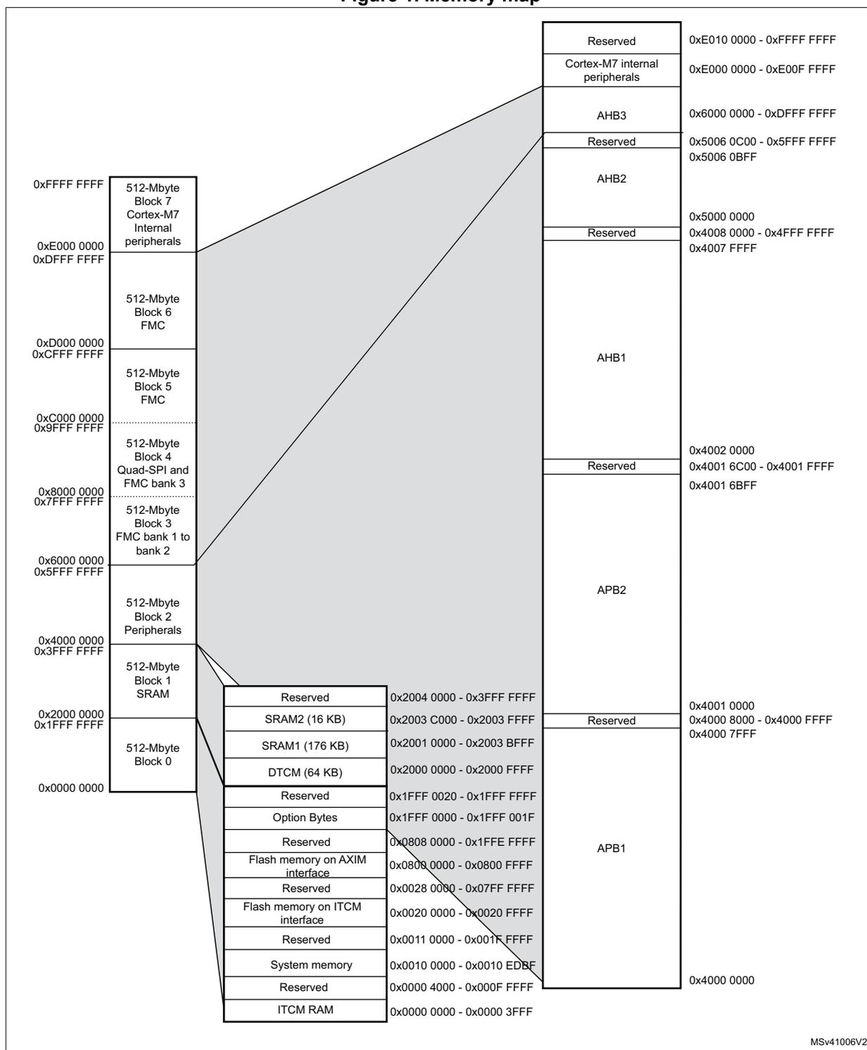
1.6 Memory organization
1.6.1 Introduction
Program memory, data memory, registers and I/O ports are organized within the same linear 4-Gbyte address space.
The bytes are coded in memory in Little Endian format. The lowest numbered byte in a word is considered the word's least significant byte and the highest numbered byte the most significant.
The addressable memory space is divided into eight main blocks, of 512 Mbytes each.
1.6.2 Memory map and register boundary addresses
Figure 1. Memory map
| 0x0000 0000 | 512-Mbyte Block 0 | ITCM RAM | 0x0000 0000 - 0x0000 3FFF |
| Reserved | 0x0000 4000 - 0x000F FFFF | ||
| System memory | 0x0010 0000 - 0x0010 EDBF | ||
| Reserved | 0x0011 0000 - 0x001F FFFF | ||
| Flash memory on ITCM interface | 0x0020 0000 - 0x0020 FFFF | ||
| Reserved | 0x0028 0000 - 0x07FF FFFF | ||
| Flash memory on AXIM interface | 0x0800 0000 - 0x0800 FFFF | ||
| Reserved | 0x0808 0000 - 0x1FFE FFFF | ||
| Option Bytes | 0x1FFF 0000 - 0x1FFF 001F | ||
| Reserved | 0x1FFF 0020 - 0x1FFF FFFF | ||
| DTCM (64 KB) | 0x2000 0000 - 0x2000 FFFF | ||
| SRAM1 (176 KB) | 0x2001 0000 - 0x2003 BFFF | ||
| SRAM2 (16 KB) | 0x2003 C000 - 0x2003 FFFF | ||
| Reserved | 0x2004 0000 - 0x3FFF FFFF | ||
| 0x2000 0000 0x1FFF FFFF | 512-Mbyte Block 1 SRAM | APB1 | 0x4000 0000 - 0x4001 6BFF |
| 0x4000 0000 0x3FFF FFFF | 512-Mbyte Block 2 Peripherals | APB2 | 0x4001 6C00 - 0x4001 FFFF |
| 0x6000 0000 0x5FFF FFFF | 512-Mbyte Block 3 FMC bank 1 to bank 2 | Reserved | 0x4002 0000 - 0x4002 0000 |
| 0x8000 0000 0x7FFF FFFF | 512-Mbyte Block 4 Quad-SPI and FMC bank 3 | Reserved | 0x4007 FFFF - 0x4008 0000 |
| 0xC000 0000 0x9FFF FFFF | 512-Mbyte Block 5 FMC | Reserved | 0x5006 0BFF - 0x5006 0C00 |
| 0xD000 0000 0xCFFF FFFF | 512-Mbyte Block 6 FMC | Reserved | 0x6000 0000 - 0xDFFF FFFF |
| 0xE000 0000 0xDFFF FFFF | 512-Mbyte Block 7 Cortex-M7 Internal peripherals | Cortex-M7 internal peripherals | 0xE000 0000 - 0xE00F FFFF |
| 0xFFFF FFFF | Reserved | 0xE010 0000 - 0xFFFF FFFF |
MSv41006V2
All the memory map areas that are not allocated to on-chip memories and peripherals are considered “Reserved”. For the detailed mapping of available memory and register areas, refer to the following table.
The following table gives the boundary addresses of the peripherals available in the devices.
Table 1. STM32F72xxx and STM32F73xxx register boundary addresses
| Boundary address | Peripheral | Bus | Register map |
|---|---|---|---|
| 0xA000 1000 - 0xA000 1FFF | QuadSPI Control Register | AHB3 | Section 13.5.14: QUADSPI register map on page 378 |
| 0xA000 0000 - 0xA000 0FFF | FMC control register | Section 12.8.6: FMC register map on page 349 | |
| 0x5006 0800 - 0x5006 0BFF | RNG | AHB2 | Section 16.7.4: RNG register map on page 458 |
| 0x5006 0000 - 0x5006 03FF | AES | Section 17.7.18: AES register map on page 510 | |
| 0x5000 0000 - 0x5003 FFFF | USB OTG FS | Section 32.15.64: OTG_FS/OTG_HS register map on page 1288 | |
| 0x4004 0000 - 0x4007 FFFF | USB OTG HS | Section 32.15.64: OTG_FS/OTG_HS register map on page 1288 | |
| 0x4002 6400 - 0x4002 67FF | DMA2 | AHB1 | Section 8.5.11: DMA register map on page 252 |
| 0x4002 6000 - 0x4002 63FF | DMA1 | ||
| 0x4002 4000 - 0x4002 4FFF | BKPSRAM | Section 5.3.27: RCC register map on page 192 | |
| 0x4002 3C00 - 0x4002 3FFF | Flash interface register | Section 3.7.9: Flash interface register map | |
| 0x4002 3800 - 0x4002 3BFF | RCC | Section 5.3.27: RCC register map on page 192 | |
| 0x4002 3000 - 0x4002 33FF | CRC | Section 11.4.6: CRC register map on page 275 | |
| 0x4002 2000 - 0x4002 23FF | GPIOI | Section 6.4.11: GPIO register map on page 212 | |
| 0x4002 1C00 - 0x4002 1FFF | GPIOH | ||
| 0x4002 1800 - 0x4002 1BFF | GPIOG | ||
| 0x4002 1400 - 0x4002 17FF | GPIOF | ||
| 0x4002 1000 - 0x4002 13FF | GPIOE | ||
| 0x4002 0C00 - 0x4002 0FFF | GPIO D | ||
| 0x4002 0800 - 0x4002 0BFF | GPIOC | ||
| 0x4002 0400 - 0x4002 07FF | GPIOB | ||
| 0x4002 0000 - 0x4002 03FF | GPIOA |
Table 1. STM32F72xxx and STM32F73xxx register boundary addresses (continued)
| Boundary address | Peripheral | Bus | Register map |
|---|---|---|---|
| 0x4000 7C00 - 0x4000 7FFF | UART8 | APB1 | Section 27.8.12: USART register map on page 950 |
| 0x4000 7800 - 0x4000 7BFF | UART7 | ||
| 0x4000 7400 - 0x4000 77FF | DAC | Section 15.5.15: DAC register map on page 447 | |
| 0x4000 7000 - 0x4000 73FF | PWR | Section 4.4.4: PWR power control register 2 (PWR_CSR2) on page 126 | |
| 0x4000 6400 - 0x4000 67FF | CAN1 | Section 31.9.5: bxCAN register map on page 1165 | |
| 0x4000 5C00 - 0x4000 5FFF | I2C3 | Section 26.9.12: I2C register map on page 886 | |
| 0x4000 5800 - 0x4000 5BFF | I2C2 | ||
| 0x4000 5400 - 0x4000 57FF | I2C1 | ||
| 0x4000 5000 - 0x4000 53FF | UART5 | Section 27.8.12: USART register map on page 950 | |
| 0x4000 4C00 - 0x4000 4FFF | UART4 | ||
| 0x4000 4800 - 0x4000 4BFF | USART3 | ||
| 0x4000 4400 - 0x4000 47FF | USART2 | ||
| 0x4000 3C00 - 0x4000 3FFF | SPI3 / I2S3 | Section 28.9.10: SPI/I2S register map on page 1010 | |
| 0x4000 3800 - 0x4000 3BFF | SPI2 / I2S2 | Section 23.4.6: IWDG register map on page 772 | |
| 0x4000 3000 - 0x4000 33FF | IWDG | Section 24.5.4: WWDG register map on page 778 | |
| 0x4000 2C00 - 0x4000 2FFF | WWDG | Section 25.6.21: RTC register map on page 822 | |
| 0x4000 2800 - 0x4000 2BFF | RTC & BKP Registers | Section 22.7.9: LPTIM register map on page 763 | |
| 0x4000 2400 - 0x4000 27FF | LPTIM1 | Section 20.5.13: TIM10/TIM11/TIM13/TIM14 register map on page 728 | |
| 0x4000 2000 - 0x4000 23FF | TIM14 | ||
| 0x4000 1C00 - 0x4000 1FFF | TIM13 | Section 20.4.14: TIM9/TIM12 register map on page 717 | |
| 0x4000 1800 - 0x4000 1BFF | TIM12 | Section 21.4.9: TIMx register map on page 742 | |
| 0x4000 1400 - 0x4000 17FF | TIM7 | ||
| 0x4000 1000 - 0x4000 13FF | TIM6 | Section 19.4.24: TIMx register map on page 677 | |
| 0x4000 0C00 - 0x4000 0FFF | TIM5 | ||
| 0x4000 0800 - 0x4000 0BFF | TIM4 | ||
| 0x4000 0400 - 0x4000 07FF | TIM3 | ||
| 0x4000 0000 - 0x4000 03FF | TIM2 |
1.7 Embedded SRAM
The STM32F72xxx and STM32F73xxx feature:
- • System SRAM up to 256 Kbytes including Data TCM RAM 64 Kbytes
- • Instruction RAM (ITCM-RAM) 16 Kbytes.
- • 4 Kbytes of backup SRAM (see section 5.1.2: Battery backup domain)
The embedded SRAM is divided into up to four blocks:
- • System SRAM:
- – SRAM1 mapped at address 0x2001 0000 and accessible by all AHB masters from AHB bus Matrix.
- – SRAM2 mapped at address 0x2003 C000 and accessible by all AHB masters from AHB bus Matrix.
- – DTCM-RAM on TCM interface (Tightly Coupled Memory interface) mapped at address 0x2000 0000 and accessible by all AHB masters from AHB bus Matrix but through a specific AHB slave bus of the CPU.
- • Instruction SRAM:
- – Instruction RAM (ITCM-RAM) mapped at address 0x0000 0000 and accessible only by CPU.
The SRAM1 and SRAM2 can be accessed as bytes, half-words (16 bits) or full words (32 bits). While DTCM and ITCM RAMs can be accessed as bytes, half-words (16 bits), full words (32 bits) or double words (64 bits). These memories can be addressed at maximum system clock frequency without wait state.
The AHB masters support concurrent SRAM accesses (from the USB OTG HS): for instance, the USB OTG HS can read/write from/to SRAM2 while the CPU is reading/writing from/to SRAM1.
1.8 Flash memory overview
The Flash memory interface manages CPU AXI and TCM accesses to the Flash memory. It implements the erase and program Flash memory operations and the read and write protection mechanisms. It accelerates code execution with ART on TCM interface or L1-Cache on AXIM interface.
The Flash memory is organized as follows:
- • A main memory block divided into sectors.
- • An information block:
- – System memory from which the device boots in System memory boot mode
- – 528 OTP (one-time programmable) bytes for user data.
- – Option bytes to configure read and write protection, BOR level, software/hardware watchdog, boot memory base address and reset when the device is in Standby or Stop mode.
Refer to Section 3: Embedded Flash memory (FLASH) for more details.
1.9 Boot configuration
In the STM32F72xxx and STM32F73xxx, two different boot areas can be selected through the BOOT pin and the boot base address programmed in the BOOT_ADD0 and BOOT_ADD1 option bytes as shown in the Table 2 .
Table 2. Boot modes
| Boot mode selection | Boot area | |
|---|---|---|
| BOOT | Boot address option bytes | |
| 0 | BOOT_ADD0[15:0] | Boot address defined by user option byte BOOT_ADD0[15:0] ST programmed value: Flash on ITCM at 0x0020 0000 |
| 1 | BOOT_ADD1[15:0] | Boot address defined by user option byte BOOT_ADD1[15:0] ST programmed value: System bootloader at 0x0010 0000 |
The values on the BOOT pin are latched on the 4th rising edge of SYSCLK after reset release. It is up to the user to set the BOOT pin after reset.
The BOOT pin is also resampled when the device exits the Standby mode. Consequently, they must be kept in the required Boot mode configuration when the device is in the Standby mode.
After startup delay, the selection of the boot area is done before releasing the processor reset.
The BOOT_ADD0 and BOOT_ADD1 address option bytes allows to program any boot memory address from 0x0000 0000 to 0x2003 FFFF which includes:
- • All Flash address space mapped on ITCM or AXIM interface
- • All RAM address space: ITCM, DTCM RAMs and SRAMs mapped on AXIM interface
- • The System memory bootloader
The BOOT_ADD0 / BOOT_ADD1 option bytes can be modified after reset in order to boot from any other boot address after next reset.
If the programmed boot memory address is out of the memory mapped area or a reserved area, the default boot fetch address is programmed as follows:
- – Boot address 0: ITCM-FLASH at 0x0020 0000
- – Boot address 1: ITCM-RAM at 0x0000 0000
When flash level 2 protection is enabled, only boot from Flash (on ITCM or AXIM interface) or system bootloader will be available. If the already programmed boot address in the BOOT_ADD0 and/or BOOT_ADD1 option bytes is out of the memory range or RAM address (on ITCM or AXIM) the default fetch will be forced from Flash on ITCM interface at address 0x00200000.
Embedded bootloader
The embedded bootloader code is located in the system memory. It is programmed by ST during production. For full information, refer to the application note (AN2606) STM32 microcontroller system memory boot mode.
By default, when the boot from system bootloader is selected, the code is executed from TCM interface. It could be executed from AXIM interface by reprogramming the BOOT_ADDx address option bytes to 0x1FF0 0000.