30. Serial audio interface (SAI)
30.1 Introduction
The SAI interface (serial audio interface) offers a wide set of audio protocols due to its flexibility and wide range of configurations. Many audio protocols can be addressed using the SAI “free protocol mode”. The free protocol mode allows the application to define the audio frame shape, number of slots, slot size, data size, and so on. For example, the SAI supports I2S standards, LSB- or MSB-justified, PCM/DSP, TDM, and AC'97 protocols.
To bring this level of flexibility and configurability, the SAI contains two audio sub-blocks that are fully independent of each other. Each audio sub-block is connected to up to 4 pins (SD, SCK, FS, MCLK). Some of these pins can be shared if the two sub-blocks are declared as synchronous to leave some free to be used as general purpose I/Os. The MCLK pin can be output, or not, depending on the application, the decoder requirement and whether the audio block is configured as the master.
The SAI can work in master or slave configuration. The audio sub-blocks can be either receiver or transmitter and can work synchronously or not (with respect to the other one).
30.2 Main features
- • Two independent audio sub-blocks which can be transmitters or receivers with their respective FIFO.
- • 8-word integrated FIFOs for each audio sub-block.
- • Synchronous or asynchronous mode between the audio sub-blocks.
- • Master or slave configuration independent for both audio sub-blocks.
- • Clock generator for each audio block to target independent audio frequency sampling when both audio sub-blocks are configured in master mode.
- • Data size configurable: 8-, 10-, 16-, 20-, 24-, 32-bit.
- • Large flexibility with “free protocol mode”, supporting several audio protocols, such as I2S, LSB- or MSB-justified, PCM/DSP, TDM, and AC’97.
- • Up to 16 slots available with configurable size and with the possibility to select which ones are active in the audio frame.
- • Number of bits by frame may be configurable.
- • Frame synchronization active level configurable (offset, bit length, level).
- • First active bit position in the slot is configurable.
- • LSB first or MSB first for data transfer.
- • Mute mode.
- • Stereo/Mono audio frame capability.
- • Communication clock strobing edge configurable (SCK).
- • Error flags with associated interrupts if enabled respectively.
- – Overrun and underrun detection,
- – Anticipated frame synchronization signal detection in slave mode,
- – Late frame synchronization signal detection in slave mode,
- – Codec not ready for the AC’97 mode in reception.
- • Interruption sources when enabled:
- – Errors,
- – FIFO requests.
- • DMA interface with 2 dedicated channels to handle access to the dedicated integrated FIFO of each SAI audio sub-block.
30.3 Functional block diagram
The block diagram of the SAI is shown in Figure 351 .
Figure 351. Functional block diagram
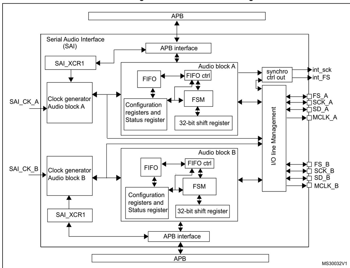
The diagram illustrates the functional architecture of the Serial Audio Interface (SAI). At the top and bottom, APB bus interfaces connect the internal SAI components to an external APB bus. The SAI contains two independent audio blocks, Audio block A and Audio block B. Each block includes a Clock generator (receiving SAI_CK_A or SAI_CK_B), a FIFO, a FIFO controller, a Configuration registers and Status register, a Functional State Machine (FSM), and a 32-bit shift register. Each block also has its own SAI_XCR1 register. An I/O line Management block on the right side manages the pins for each audio block, providing signals like int_sck, int_FS, FS_A, SCK_A, SD_A, MCLK_A for Audio block A, and FS_B, SCK_B, SD_B, MCLK_B for Audio block B. A 'synchro ctrl out' block is also shown. The diagram is labeled MS30032V1 in the bottom right corner.
The SAI is mainly composed of two audio sub-blocks with their own clock generator. Each audio block integrates a 32-bit shift register controlled by their own functional state machine. Data are stored or read from the dedicated FIFO. FIFO may be accessed by the CPU, or by DMA in order to leave the CPU free during the communication. Each audio block is independent. They can be synchronous with each other.
An I/O line controller manages each dedicated pins for a given audio block in the SAI. If the two blocks are synchronized, this controller reduces the number of I/Os used, freeing up an FS pin, an SCK pin and eventually an MCLK pin, making them general purpose I/Os.
The functional state machine can be configured to address a wide range of audio protocols. Some registers are present to set-up the desired protocols (audio frame waveform generator).
The audio block can be a transmitter or receiver, in master or slave mode. The master mode means the bit clock SCK and the frame synchronization signal are generated from the SAI, whereas in slave mode, they come from another external or internal master. There is a particular case for which the FS signal direction is not directly linked to the master or slave mode definition. In AC'97 protocol, it will be an SAI output even if the SAI (link controller) is set-up to consume the SCK clock (and so to be in Slave mode).
30.4 Main SAI modes
Each audio sub-block of the SAI can be configured to be master or slave via bit MODE[0] in the SAI_xCR1 register of the selected audio block.
In master mode:
- • The bit clock is generated by the SAI using the clock generator on pin SCK_A or SCK_B (depending which audio block is declared as a master in the SAI).
- • The dedicated pin SCK_x is considered as an output.
In slave mode:
- • The slave must be enabled before the master is enabled.
- • The slave audio block's SCK clock I/O pin is considered input if it is configured in asynchronous mode.
- • If the audio block is declared synchronous with the second audio block in the SAI, its SCK I/O pin is released to leave it free to be used as a general purpose I/O and is connected internally to the SCK pin of the device with which it will be synchronized.
Each audio block can use a different audio protocol. When PRTCFCG[1:0] of the SAI_xCR1 register is set to 0, the free protocol mode is selected and each SAI sub-block can emulate I2S standards, LSB- or MSB-justified, PCM/DSP, TDM, or AC'97 protocols.
Each audio sub-block can be independently defined as a transmitter or receiver by bit MODE[1] in the SAI_xCR1 register of the relevant audio block. The I/O pin SD will be defined respectively as an output or an input.
It is possible to declare two master audio blocks in the same SAI with two different MCLK and SCK clock frequencies (they have to be declared asynchronous).
Each of the audio blocks in the SAI are enabled by bit SAIxEN in the SAI_xCR1 register. As soon as this bit is active, the transmitter or the receiver is sensitive to the activity on the clock line, data line and synchronization line in slave mode.
In master TX mode, enabling the audio block immediately generates the bit clock for the external slaves even if there is no data in the FIFO. However FS signal generation is conditioned by the presence of data in the FIFO. After the FIFO receives the first data to transmit, this data is output to external slaves. If there is no data to transmit in the FIFO, 0 values are then sent in the audio frame with an underrun flag generation.
In slave mode, the audio frame starts when the audio block is enabled and when a start of frame is detected.
In Slave TX mode, no underrun event is possible on the first frame after the audio block is enabled, because the mandatory operating sequence in this case is:
- 1. Write into the SAI_xDR (by software or by DMA).
- 2. Wait until the FIFO threshold (FLH) flag is different from 000b (FIFO empty).
- 3. Enable the audio block in slave transmitter mode.
30.5 SAI synchronization mode
Internal synchronization
An audio block can be declared synchronous with the second audio block. In this case, the bit clock and the frame synchronization signals are shared to reduce the number of external pins used for the communication. The audio block declared as synchronous with the other one will see its own SCK_x, FS_x, and MCLK_x pins released to bring them back as GPIOs. The one declared asynchronous is the one for which the I/O pins FS_x and SCK_x and MCLK_x (if the audio block is considered as master) are considered.
Typically, the audio block synchronous mode may be used to configure the SAI in full duplex mode. One of the two audio blocks can be configured as master and the other as slave, or both can be slaves; with one block declared as asynchronous (respective bit SYNCEN[1:0] = 00 in SAI_xCR1) and the other one declared as synchronous with the other audio block (respective bit SYNCEN[1:0] = 01 in the SAI_xCR1).
Note: APB frequency PCLK must be greater or equal to twice the bit rate clock frequency (due to internal resynchronization stages).
30.6 Audio data size
The audio frame can target different data sizes by configuring bit DS[2:0] in the SAI_xCR1 register. The data sizes may be 8-, 10-, 16-, 20-, 24- or 32-bit. During the transfer, either the MSB or the LSB of the data are sent first, depending on the configuration of bit LSBFIRST in the SAI_xCR1 register.
30.7 Frame synchronization
The FS signal acts as the Frame synchronization signal in the audio frame (start of frame). The shape of this signal is completely configurable in order to target the different audio protocols with their own specificities concerning this Frame synchronization behavior. This configurability is done using register SAI_xFRCR. Figure 352 gives a view of this flexibility.
Figure 352. Audio frame
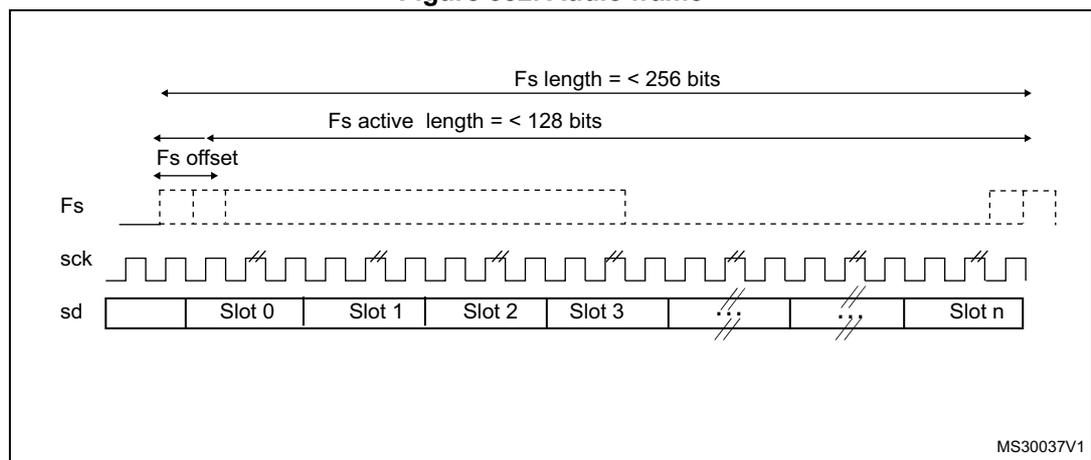
The diagram illustrates the timing of an audio frame. The top signal is the Frame Synchronization (Fs) signal, which is a periodic pulse. The period of this signal is labeled 'Fs length = < 256 bits'. The duration of the active part of the signal is labeled 'Fs active length = < 128 bits'. The time interval between the start of one active Fs pulse and the start of the next is labeled 'Fs offset'. Below the Fs signal is the serial clock (sck) signal, shown as a square wave. The bottom signal is the serial data (sd) signal, which is divided into slots: Slot 0, Slot 1, Slot 2, Slot 3, followed by ellipses, and then Slot n. Each slot corresponds to a data sample. The diagram is labeled with 'MS30037V1' in the bottom right corner.
In AC'97 mode (bit PRTCFCFG[1:0] = 10 in the SAI_xCR1 register), the frame synchronization shape is forced to be configured to target these protocols. The SAI_xFRCR register value is ignored.
Each audio block is independent and so each requires a specific configuration.
30.7.1 Frame length
- • Master mode: The audio frame length can be configured up to 256 bit clock, setting bit FRL[7:0] in the SAI_xFRCR register. If the frame length is greater than the number of declared slots for the frame, the remaining bits to transmit will be extended to 0 or the SD line will be released to HI-z depending the state of bit TRIS in the SAI_xCR2 register (refer to Section 30.12.4 ). In reception mode, the remaining bit is ignored.
- • Slave mode: The audio frame length is mainly used in order to specify to the slave the number of bit clocks per audio frame sent by the external master. It is used mainly to detect from the master, any anticipated or late occurrence of the Frame synchronization signal during an on-going audio frame. An error will be generated in such case. For more details please refer to the Section 30.13 .
The number of bits in the frame is equal to FRL[7:0] + 1.
The minimum number of bits to transfer in an audio frame is 8. This is the case when the data size is 8-bit and only one slot is defined in NBSLOT[3:0] in the SAI_xSLOTR register (NBSLOT[3:0] = 0000 for slot 0).
In master mode:
- • If bit NODIV in the SAI_xCR1 register is cleared, the frame length should be aligned to a number equal to a power of 2, from 8 to 256. This is to ensure that an audio frame contains an integer number of MCLK pulses per bit clock, which ensures correct operation of the external DAC/ADC inside the decoders. If the value set in FRL[7:0] does not respect this rule, flag WCKCFG is set when the audio block is enabled and an interrupt is generated if bit WCKCFGIE is set in the SAI_xIM register. The SAI is automatically disabled.
- • If bit NODIV in the SAI_xCR1 register is set, the FRL[7:0] bit can take any of the values without constraint since the input clock of the audio block should be equal to the bit clock. There is no MCLK_x clock which can be output. MCLK_x output pad is automatically disabled.
In slave mode, there are no constraints for the FRL[7:0] bit configuration in the SAI_xFRCR register.
30.7.2 Frame synchronization polarity
Bit FSPOL in the SAI_xFRCR register sets the active polarity of the FS pin from which a frame is started. The start of frame is edge sensitive.
In slave mode, the audio block waits for a valid frame to start to transmit or to receive. Start of frame is synchronized to this signal. It is effective only if the start of frame is not detected during an on-going communication and assimilated to an anticipated start of frame (refer to Section 30.13 ).
In master mode, the frame synchronization is sent continuously each time an audio frame is complete until the SAIxEN bit in the SAI_xCR1 register is cleared. If no data is present in the FIFO at the end of the previous audio frame, an underrun condition will be managed as
described in Section 30.13 ), but there will be no interruption in the audio communication flow.
30.7.3 Frame synchronization active level length
Bit FSALL[6:0] in the SAI_xFRCR register configures the length of the active level of the Frame synchronization signal. The length can be set from 1 to 128 bit clock SCK.
The active length may be half of the frame length in I2S, LSB or MSB-justified modes for instance, or one-bit wide for PCM/DSP or TDM mode, or even 16-bit length in AC'97.
30.7.4 Frame synchronization offset
Depending on the audio protocol targeted in the application, the Frame synchronization signal can be asserted when transmitting the last bit or the first bit of the audio frame (as for instance, respectively, in I2S standard protocol and in MSB-justified protocol). Bit FSOFF in the SAI_xFRCR register makes the choice.
30.7.5 FS signal role
The FS signal may have a different meaning depending on the FS function. Bit FSDEF in the SAI_xFRCR register selects which meaning it will have. It may be either:
- • 0: a start of frame, like for instance the PCM/DSP, TDM, AC'97, audio protocols,
- • 1: a start of frame and a channel side identification within the audio frame like for the I2S, the MSB or LSB-justified protocols.
When the FS signal is considered as a start of frame and channel side identification within the frame, the number of declared slots must be considered to be half of the number for the left channel and half of the number for the right channel. If the number of bit clock on half audio frame is greater than the number of slots dedicated to a channel side, if TRIS = 0, 0 is sent for transmission for the remaining bit clock in the SAI_xCR2 register, otherwise if TRIS = 1, the SD line is released to HI-Z. In reception, the remaining bit clock are not considered until the channel side changes.
Figure 353. FS role is start of frame + channel side identification (FSDEF = TRIS = 1)
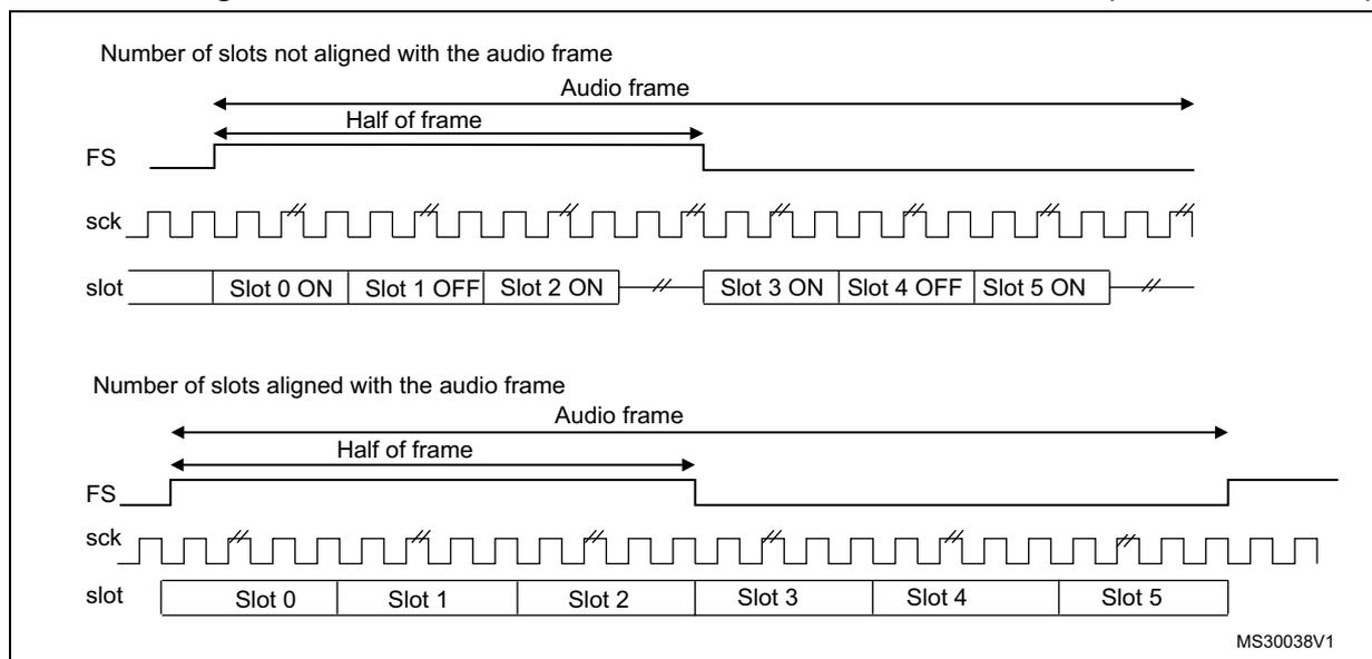
- 1. The frame length should be even.
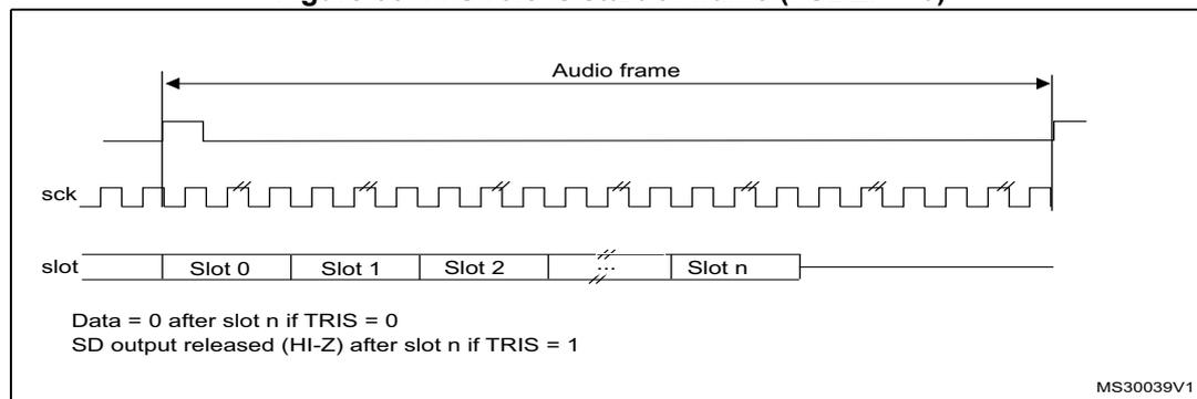
If bit FSDEF in SAI_xFCR is kept clear, so FS signal is equivalent to a start of frame, and if the number of slots defined in bit NBSLOT[3:0] in SAI_xSLOTR multiplied by the number of bits by slot configured in bit SLOTSZ[1:0] in SAI_xSLOTR is less than the frame size (bit FRL[7:0] in the SAI_xFCR register), then,
- • if TRIS = 0 in the SAI_xCR2 register, the remaining bit after the last slot will be forced to 0 until the end of frame in case of transmission,
- • if TRIS = 1, the line will be released to HI-Z during the transfer of these remaining bits. In reception mode, these bits are discarded.
Figure 354. FS role is start of frame (FSDEF = 0)
30.8 Slot configuration
The slot is the basic element in the audio frame. The number of slots in the audio frame is equal to the configured setting of bit NBSLOT[3:0] in the SAI_xSLOTR register + 1. The maximum number of slots per audio frame is fixed at 16.
For AC'97 protocol (when bit PRTCFC[1:0] = 10), the number of slots is automatically set to target the protocol specification, and the value of NBSLOT[3:0] is ignored.
Each slot can be defined as a valid slot, or not, by setting bit SLOTEN[15:0] in the SAI_xSLOTR register. In an audio frame, during the transfer of a non-valid slot, 0 value will be forced on the data line or the SD data line will be released to HI-Z (refer to Section 30.12.4 ) if the audio block is transmitter, or the received value from the end of this slot will be ignored. Consequently, there will be no FIFO access and so no request to read or write the FIFO linked to this inactive slot status.
The slot size is also configurable as shown in the Figure 355 . The size of the slots is selected by setting bit SLOTSZ[1:0] in the SAI_xSLOTR register. The size is applied identically for each slot in an audio frame.
Figure 355. Slot size configuration with FBOFF = 0 in SAI_xSLOTR
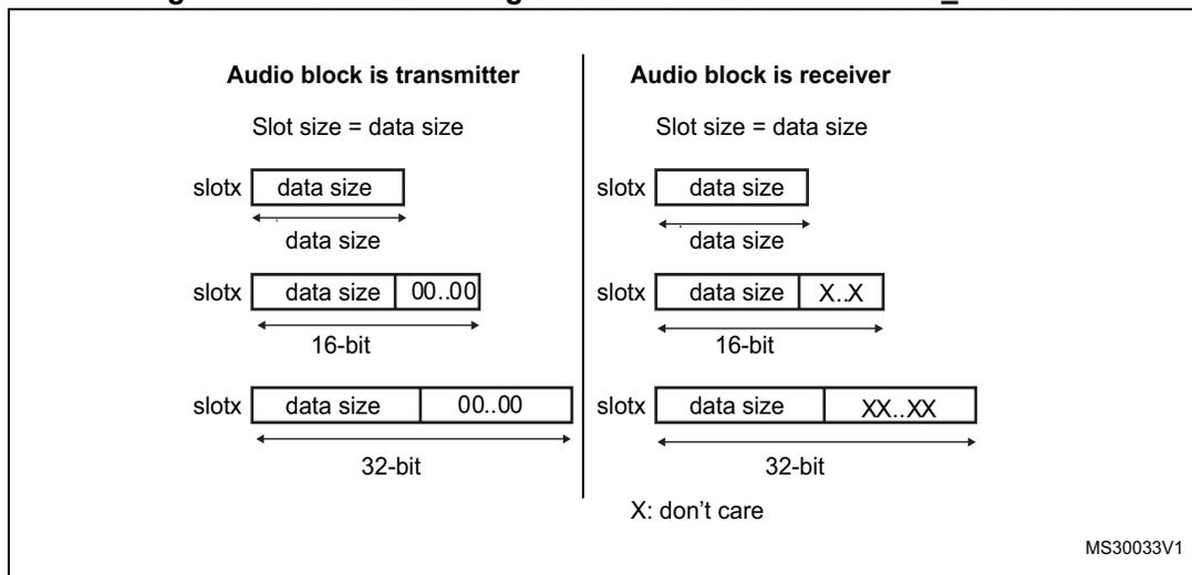
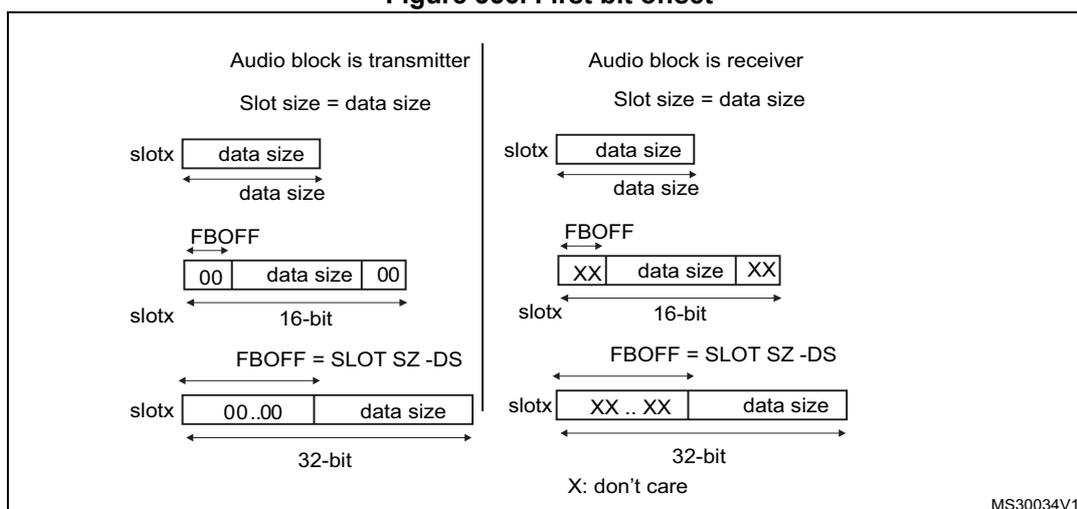
It is possible to choose the position of the first data bit to transfer within the slots, this offset is configured by bit FBOFF[5:0] in the SAI_xSLOTR register. 0 values will be injected in transmitter mode from the beginning of the slot until this offset position is reached. In reception, the bit in the offset phase is ignored. This feature targets the LSB justified protocol (if the offset is equal to the slot size minus the data size).
Figure 356. First bit offset
It is mandatory to respect the following conditions in order to avoid bad SAI behavior:
The number of slots should be even when bit FSDEF in the SAI_xFRCR register is set.
In AC'97 (bit PRTCFG[1:0] = 10), the slot size is automatically set as defined in Section 30.11 .
30.9 SAI clock generator
Each audio block has its own clock generator to make these two blocks completely independent. There is no difference in terms of functionality between these two clock generators. They are exactly the same.
When the audio block is defined as Master, the clock generator generates the communication clock (the bit clock) and the master clock for external decoders.
When the audio block is defined as slave, the clock generator is OFF.
Figure 357 illustrates the architecture of the audio block clock generator.
Figure 357. Audio block clock generator overview
![Figure 357: Audio block clock generator overview. The diagram shows the internal architecture of the SAI clock generator. It starts with the SAI_CK_x input clock. This clock is divided by a 'Master clock divider' block, which is controlled by the MCKDIV[3:0] register. The output of this divider is connected to a multiplexer (MUX) labeled 'NODIV'. The MUX has two inputs: '0' (direct connection) and '1' (divided by 2). The output of this MUX is the MCLK_x signal. The same SAI_CK_x input clock is also connected to a 'Bit clock divider' block, which is controlled by the FRL[7:0] register. The output of the bit clock divider is connected to another MUX labeled 'NODIV'. This MUX also has two inputs: '0' (direct connection) and '1' (divided by 2). The output of this MUX is the SCK_x signal. The diagram is labeled MS30040V1.](/RM0430-STM32F413-423/231dedb7a56c3807733b297a26e9f7be_img.jpg)
Note: If NoDiv is set to 1, the MCLK_x signal will be set at 0 level if this pin is configured as the SAI pin in GPIO peripherals.
The clock source for the clock generator comes from the product clock controller. The SAI_CK_x clock is equivalent to the master clock which may be divided for the external decoders using bit MCKDIV[3:0]:
MCLK_x signal is used only in TDM.
The division must be even in order to keep 50% on the Duty cycle on the MCLK output and on the SCK_x clock. If bit MCKDIV[3:0] = 0000, division by one is applied to have \( \text{MCLK\_x} = \text{SAI\_CK\_x} \) .
In the SAI, the single ratio \( \text{MCLK/FS} = 256 \) is considered. Mostly, three frequency ranges will be encountered as illustrated in the Table 183 .
Table 183. Example of possible audio frequency sampling range
| Input SAI_CK_x clock frequency | Most usual audio frequency sampling achievable | MCKDIV[3:0] |
|---|---|---|
| 192 kHz x 256 | 192 kHz | MCKDIV[3:0] = 0000 |
| 96 kHz | MCKDIV[3:0] = 0001 | |
| 48 kHz | MCKDIV[3:0] = 0010 | |
| 16 kHz | MCKDIV[3:0] = 0100 | |
| 8 kHz | MCKDIV[3:0] = 1000 | |
| 44.1 kHz x 256 | 44.1 kHz | MCKDIV[3:0] = 0000 |
| 22.05 kHz | MCKDIV[3:0] = 0001 | |
| 11.025 kHz | MCKDIV[3:0] = 0010 | |
| SAI_CK_x = MCLK (1) | MCLK | MCKDIV[3:0] = 0000 |
1. This may happen when the product clock controller selects an external clock source, instead of PLL clock.
The master clock may be generated externally on an I/O pad for external decoders if the corresponding audio block is declared as master with bit NODIV = 0 in the SAI_xCR1 register. In slave, the value set in this last bit is ignored since the clock generator is OFF, and the MCLK_x I/O pin is released for use as a general purpose I/O.
The bit clock is derived from the master clock. The bit clock divider sets the divider factor between the bit clock SCK_x and the master clock MCLK_x following the formula:
where:
256 is the fixed ratio between MCLK and the audio frequency sampling.
FRL[7:0] is the number of bit clock - 1 in the audio frame, configured in the SAI_xFCR register.
It is mandatory in master mode that (FRL[7:0] + 1) should be equal to a number with a power of 2 (refer to Section 30.7 ) in order to have an even integer number of MCLK_x pulses by bit clock. The 50% duty cycle is guaranteed on the bit clock SCK_x.
The SAI_CK_x clock can be also equal to the bit clock frequency. In this case, bit NODIV in the SAI_xCR1 register should be set and the value inside the MCKDIV divider and the bit clock divider will be ignored. In this case, the number of bits per frame is fully configurable without the need to be equal to a power of two.
The bit clock strobing edge on SCK can be configured by bit CKSTR in the SAI_xCR1 register.
30.10 Internal FIFOs
Each audio block in the SAI has its own FIFO. Depending if the block is defined to be a transmitter or a receiver, the FIFO will be written or read, respectively. There is therefore only one FIFO request linked to FREQ bit in the SAI_xSR register.
An interrupt is generated if FREQIE bit is enabled in the SAI_xIM register. This depends on:
- • FIFO threshold setting (FLTH bits in SAI_CR2)
- • Communication direction transmitter or receiver (see Section : Interrupt generation in transmitter mode and Section : Interrupt generation in reception mode )
Interrupt generation in transmitter mode
The interrupt generation depends on the FIFO configuration in transmitter mode:
- • When the FIFO threshold bits in SAI_XCR2 register are configured as FIFO empty (FTH[2:0] set to 000b), an interrupt is generated (FREQ bit set by hardware to 1 in SAI_XSR register) if no data are available in SAI_xDR register (FLTH[2:0] bits in SAI_xSR is less than 001b). This Interrupt (FREQ bit in SAI_XSR register) is cleared by hardware when the FIFO became not empty (FLTH[2:0] bits in SAI_xSR are different from 000b) i.e one or more data are stored in the FIFO.
- • When the FIFO threshold bits in SAI_XCR2 register are configured as FIFO quarter full (FTH[2:0] set to 001b), an interrupt is generated (FREQ bit set by hardware to 1 in SAI_XSR register) if less than a quarter of the FIFO contains data (FLTH[2:0] bits in SAI_xSR are less than 010b). This Interrupt (FREQ bit in SAI_XSR register) is cleared by hardware when at least a quarter of the FIFO contains data (FLTH[2:0] bits in SAI_xSR are higher or equal to 010b).
- • When the FIFO threshold bits in SAI_XCR2 register are configured as FIFO half full (FTH[2:0] set to 010b), an interrupt is generated (FREQ bit set by hardware to 1 in SAI_XSR register) if less than half of the FIFO contains data (FLTH[2:0] bits in SAI_xSR are less than 011b). This Interrupt (FREQ bit in SAI_XSR register) is cleared by hardware when at least half of the FIFO contains data (FLTH[2:0] bits in SAI_xSR are higher or equal to 011b).
- • When the FIFO threshold bits in SAI_XCR2 register are configured as FIFO three quarter (FTH[2:0] set to 011b), an interrupt is generated (FREQ bit is set by hardware to 1 in SAI_XSR register) if less than three quarters of the FIFO contain data (FLTH[2:0] bits in SAI_xSR are less than 100b). This Interrupt (FREQ bit in SAI_XSR register) is cleared by hardware when at least three quarters of the FIFO contain data (FLTH[2:0] bits in SAI_xSR are higher or equal to 100b).
- • When the FIFO threshold bits in SAI_XCR2 register are configured as FIFO full (FTH[2:0] set to 100b), an interrupt is generated (FREQ bit is set by hardware to 1 in SAI_XSR register) if the FIFO is not full (FLTH[2:0] bits in SAI_xSR is less than 101b). This Interrupt (FREQ bit in SAI_XSR register) is cleared by hardware when the FIFO is full (FLTH[2:0] bits in SAI_xSR is equal to 101b value).
Interrupt generation in reception mode
The interrupt generation depends on the FIFO configuration in reception mode:
- • When the FIFO threshold bits in SAI_XCR2 register are configured as FIFO empty (FTH[2:0] set to 000b), an interrupt is generated (FREQ bit is set by hardware to 1 in SAI_XSR register) if at least one data is available in SAI_xDR register (FLTH[2:0] bits in SAI_xSR is higher or equal to 001b). This Interrupt (FREQ bit in SAI_XSR register) is cleared by hardware when the FIFO became empty (FLTH[2:0] bits in SAI_xSR is equal to 000b) i.e no data is stored in FIFO.
- • When the FIFO threshold bits in SAI_XCR2 register are configured as FIFO quarter fully (FTH[2:0] set to 001b), an interrupt is generated (FREQ bit is set by hardware to 1 in SAI_XSR register) if at less one quarter of the FIFO data locations are available
(FLTH[2:0] bits in SAI_xSR is higher or equal to 010b). This Interrupt (FREQ bit in SAI_xSR register) is cleared by hardware when less than a quarter of the FIFO data locations become available (FLTH[2:0] bits in SAI_xSR is less than 010b).
- • When the FIFO threshold bits in SAI_xCR2 register are configured as FIFO half fully (FTH[2:0] set to 010b value), an interrupt is generated (FREQ bit is set by hardware to 1 in SAI_xSR register) if at least half of the FIFO data locations are available (FLTH[2:0] bits in SAI_xSR is higher or equal to 011b). This Interrupt (FREQ bit in SAI_xSR register) is cleared by hardware when less than half of the FIFO data locations become available (FLTH[2:0] bits in SAI_xSR is less than 011b).
- • When the FIFO threshold bits in SAI_xCR2 register are configured as FIFO three quarter full (FTH[2:0] set to 011b value), an interrupt is generated (FREQ bit is set by hardware to 1 in SAI_xSR register) if at least three quarters of the FIFO data locations are available (FLTH[2:0] bits in SAI_xSR is higher or equal to 100b). This Interrupt (FREQ bit in SAI_xSR register) is cleared by hardware when the FIFO has less than three quarters of the FIFO data locations available (FLTH[2:0] bits in SAI_xSR is less than 100b).
- • When the FIFO threshold bits in SAI_xCR2 register are configured as FIFO full (FTH[2:0] set to 100b), an interrupt is generated (FREQ bit is set by hardware to 1 in SAI_xSR register) if the FIFO is full (FLTH[2:0] bits in SAI_xSR is equal to 101b). This Interrupt (FREQ bit in SAI_xSR register) is cleared by hardware when the FIFO is not full (FLTH[2:0] bits in SAI_xSR is less than 101b).
Like interrupt generation, the SAI can use the DMA if DMAEN bit in the SAI_xCR1 register is set. The FREQ bit assertion mechanism is the same as the interruption generation mechanism described above for FREQIE.
Each FIFO is an 8-word FIFO. Each read or write operation from/to the FIFO targets one word FIFO allocation whatever the access size. Each FIFO word contains one audio frame. FIFO pointers are incremented by one word after each access to the SAI_xDR register.
Data should be right aligned when it is written in the SAI_xDR.
Data received will be right aligned in the SAI_xDR.
The FIFO pointers can be reinitialized when the SAI is disabled by setting bit FFLUSH in the SAI_xCR2 register. If FFLUSH is set when the SAI is enabled the data present in the FIFO will be lost automatically.
30.11 AC'97 link controller
The SAI is able to work as an AC'97 link controller. In this protocol:
- • The slot number and the slot size are fixed.
- • The frame synchronization signal is perfectly defined and has a fixed shape.
To select this protocol, set bit PRTCFCFG[1:0] in the SAI_xCR1 register to 10. When AC'97 mode is selected the data sizes that can be used are 16-bit or 20-bit only, else SAI behavior is not guaranteed.
- • Bits NBSLOT[3:0] and SLOTSZ[1:0] are consequently ignored.
- • The number of slots is fixed at 13 slots. The first one is 16 bits wide and all the others are 20 bits wide (data slots).
- • Bit FBOFF[5:0] in the SAI_xSLOTR register is ignored
- • The SAI_xFRCR register is ignored.
The FS signal from the block defined as asynchronous is configured automatically as an output, since the AC'97 controller link drives the FS signal whatever the master or slave configuration.
Figure 358 presents an AC'97 audio frame structure.
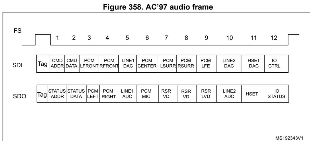
Figure 358. AC'97 audio frame
| FS | 1 2 3 4 5 6 7 8 9 10 11 12 | ||||||||||||
| SDI | Tag | CMD ADDR | CMD DATA | PCM LFRONT | PCM RFRONT | LINE1 DAC | PCM CENTER | PCM LSURR | PCM RSURR | PCM LFE | LINE2 DAC | HSET DAC | IO CTRL |
| SDO | Tag | STATUS ADDR | STATUS DATA | PCM LEFT | PCM RIGHT | LINE1 ADC | PCM MIC | RSR VD | RSR VD | RSR LVD | LINE2 ADC | HSET | IO STATUS |
MS192343V1
Note: In AC'97 protocol, bit 2 of the tag is reserved (always 0), so whatever the value written in the SAI FIFO, bit 2 of the TAG is forced to 0 level.
For more details about TAG representation, please refer to the AC'97 protocol standard.
One SAI can be used to target an AC'97 point-to-point communication.
In receiver mode, the SAI acting as an AC'97 link controller will require no FIFO request and so no data storage in the FIFO when the codec ready bit in the slot 0 is decoded low. If bit CNRDYIE is enabled in the SAI_xIM register, flag CNRDY will be set in the SAI_xSR register and an interrupt is generated. This flag is dedicated to the AC'97 protocol.
30.12 Specific features
The SAI has some specific functions which can be useful depending on the audio protocol selected. These functions are accessible through specific bits in the SAI_xCR2 register.
30.12.1 Mute mode
Mute mode may be used when the audio block is a transmitter or receiver.
Transmitter
In transmitter mode, Mute mode can be selected at anytime. Mute mode is active for entire audio frames. The bit MUTE in the SAI_xCR2 register requests Mute mode when it is set during an on-going frame.
The mute mode bit is strobed only at the end of the frame. If set at this time, the mute mode is active at the beginning of the new audio frame, for a complete frame, until the next end of frame, it then strobes the bit to determine if the next frame will still be a mute frame.
If the number of slots set in bit NBSLOT[3:0] in the SAI_xSLOTR register is lower than or equal to two, it is possible to specify if the value sent during the Mute mode is 0 or if it is the last value of each slot. The selection is done via bit MUTEVAL in the SAI_xCR2 register.
If the number of slots set in bit NBSLOT[3:0] in the SAI_xSLOTR register is greater than two, MUTEVAL bit in the SAI_xCR2 has no meaning as 0 values are sent on each bit on each slot.
During Mute mode, the FIFO pointers are still incremented, meaning that data which was present in the FIFO and for which the Mute mode is requested is discarded.
Receiver
In receiver mode, it is possible to detect a Mute mode sent from the external transmitter when all the declared and valid slots of the audio frame receive 0 for a given consecutive number of audio frames (bit MUTECNT[5:0] in the SAI_xCR2 register).
When the number of MUTE frames is detected, flag MUTEDET in the SAI_xSR register is set and an interrupt can be generated if bit MUTEDETIE is set in the SAI_xCR2.
The mute frame counter is cleared when the audio block is disabled or when a valid slot receives at least one data in an audio frame. The interrupt is generated just once, when the counter reaches the specified value in bit MUTECNT[5:0]. Then the interrupt event is re-armed when the counter is cleared.
30.12.2 MONO/STEREO function
In transmission mode, it is possible to address the Mono mode without any data pre-processing in memory when the number of slot is equal to 2 (NBSLOT[3:0] = 0001 in the SAI_xSLOTR). In such a case, the access to and from the FIFO will be reduced by two since in transmission, the data for slot 0 is duplicated into data slot 1.
To select the Mono feature, set bit MONO in the SAI_xCR1 register.
In reception mode, bit MONO can be set and has a meaning only if the number of slots is equal to 2 like for the transmission mode. When it is set, only the data of slot 0 will be stored in the FIFO. The data belonging to slot 1 will be discarded since in this case, it is supposed to be the same as the previous slot. If the data flux in reception is a real stereo audio flow with a distinct and different left and right data, bit MONO has no meaning. The conversion from the output stereo file to the equivalent mono file is done by software.
Note: To enable Mono mode, NBSLOT and SLOTEN must equal two and MONO bit set to 1.
30.12.3 Companding mode
Telecommunication applications may require to process the data to transmit or to receive with a data companding algorithm.
Depending on the COMP[1:0] bit in the SAI_xCR2 register (used only when TDM mode is selected), the software may choose to process or not the data before sending it on SD serial output line (compression) or to expand the data after the reception on SD serial input line (expansion) as illustrated in Figure 359. The two companding modes supported are the \( \mu \) -Law and the A-Law log which are a part of the CCITT G.711 recommendation.
The companding standard employed in the United States and Japan is the \( \mu \) -Law and allows 14 bits of dynamic range (COMP[1:0] = 10 in the SAI_xCR2 register).
The European companding standard is A-Law and allows 13 bits of dynamic range (COMP[1:0] = 11 in the SAI_xCR2 register).
Companding standard ( \( \mu \) -Law or A-Law) can be computed based on 1’s complement or 2’s complement representation depending on the CPL bit setting in the SAI_xCR2 register.
The \( \mu \) -Law and A-Law formats encode data into 8-bit code elements with MSB alignment. Companded data is always 8 bits wide. For this reason, bit DS[2:0] in the SAI_xCR1 register will be forced to 010 when the SAI audio block is enabled (bit SAIxEN = 1 in the SAI_xCR1 register) and when the COMP[1:0] bit selects one of these two companding modes.
If no companding processing is required, COMP[1:0] bit in the SAI_xCR2 register should be kept cleared.
Figure 359. Data companding hardware in an audio block in the SAI
![Figure 359: Data companding hardware in an audio block in the SAI. The diagram shows two modes: Receiver mode (bit MODE[0] = 1 in SAI_xCR1) and Transmitter mode (bit MODE[0] = 0 in SAI_xCR1). In Receiver mode, data from the SD line enters a 32-bit shift register, then passes through an 'expand' block, and finally into a FIFO. A multiplexer controlled by COMP[1] selects between the FIFO output and the 'expand' block output. In Transmitter mode, data from a FIFO passes through a 'compress' block, then into a multiplexer controlled by COMP[1], and finally into a 32-bit shift register which outputs to the SD line.](/RM0430-STM32F413-423/3ef99712d874e50e56a704e2e2a610ac_img.jpg)
The diagram illustrates the data flow for companding in the SAI audio block. It is divided into two sections: Receiver mode and Transmitter mode.
- Receiver mode (bit MODE[0] = 1 in SAI_xCR1): The data flow starts from the SD line, entering a 32-bit shift register. The output of the shift register goes to both an 'expand' block and a bypass path. A multiplexer controlled by COMP[1] selects between the bypass path (input 0) and the 'expand' block output (input 1). The output of the multiplexer goes to a FIFO.
- Transmitter mode (bit MODE[0] = 0 in SAI_xCR1): The data flow starts from a FIFO, entering both a 'compress' block and a bypass path. A multiplexer controlled by COMP[1] selects between the bypass path (input 0) and the 'compress' block output (input 1). The output of the multiplexer goes to a 32-bit shift register, which then outputs to the SD line.
MS19244V1
Note: Not applicable when AC’97 selected.
Expansion or compression mode is automatically selected by the SAI configuration.
- • If the SAI audio block is configured to be a transmitter, and if the COMP[1] bit is set in the SAI_xCR2 register, the compression mode will be applied.
- • If the SAI audio block is declared as a receiver, the expansion algorithm will be applied.
30.12.4 Output data line management on an inactive slot
In transmitter mode, it is possible to choose the behavior of the SD line in output when an inactive slot is sent on the data line (via bit TRIS in the SAI_xCR2 register when the SAI is disabled).
- • Either the SAI forces 0 on the SD output line when an inactive slot is transmitted, or
- • The line is released in HI-z state at the end of the last bit of data transferred, to release the line for other transmitters connected to this node.
It is important to note that the two transmitters do not attempt to drive the same SD output pin simultaneously, which could result in a short circuit. In order to ensure a gap between transmissions, if the data is lower than 32-bit, the data can be extended to 32-bit by setting bit SLOTSZ[1:0] = 10 in the SAI_xSLOTR register. Then, the SD output pin will be tristated at the end of the LSB of the active slot (during the padding to 0 phase to extend the data to 32-bit) if the following slot is declared inactive.
In addition, if the number of slots multiplied by the slot size is lower than the frame length, the SD output line will be tristated when the padding to 0 is done to complete the audio frame.
Figure 360 illustrates these behaviors.
Figure 360. Tristate strategy on SD output line on an inactive slot
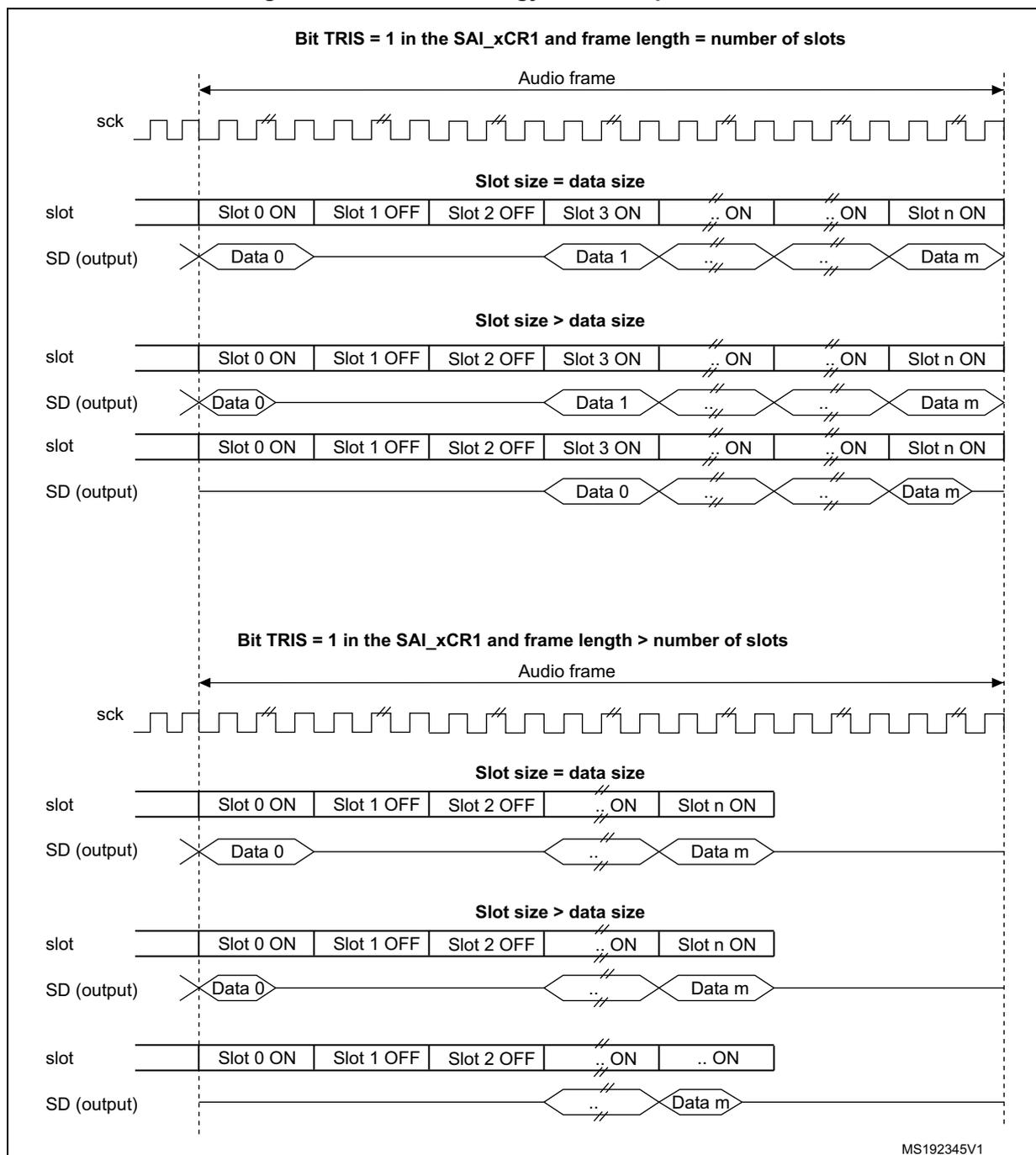
Bit TRIS = 1 in the SAI_xCR1 and frame length = number of slots
Audio frame
sck
Slot size = data size
slot Slot 0 ON Slot 1 OFF Slot 2 OFF Slot 3 ON ... ON ... ON Slot n ON
SD (output) Data 0 Data 1 ... Data m
Slot size > data size
slot Slot 0 ON Slot 1 OFF Slot 2 OFF Slot 3 ON ... ON ... ON Slot n ON
SD (output) Data 0 Data 1 ... Data m
slot Slot 0 ON Slot 1 OFF Slot 2 OFF Slot 3 ON ... ON ... ON Slot n ON
SD (output) Data 0 ... Data m
Bit TRIS = 1 in the SAI_xCR1 and frame length > number of slots
Audio frame
sck
Slot size = data size
slot Slot 0 ON Slot 1 OFF Slot 2 OFF ... ON Slot n ON
SD (output) Data 0 ... Data m
Slot size > data size
slot Slot 0 ON Slot 1 OFF Slot 2 OFF ... ON Slot n ON
SD (output) Data 0 ... Data m
slot Slot 0 ON Slot 1 OFF Slot 2 OFF ... ON .. ON
SD (output) ... Data m
MS192345V1
When the selected audio protocol uses the FS signal as a start of frame and a channel side identification (bit FSDEF = 1 in the SAI_xFRCR register), the tristate mode is managed according to Figure 361 (where bit TRIS in the SAI_xCR1 register = 1, and FSDEF=1, and half frame length > number of slots/2, and NBSLOT=6).
Figure 361. Tristate on output data line in a protocol like I2S
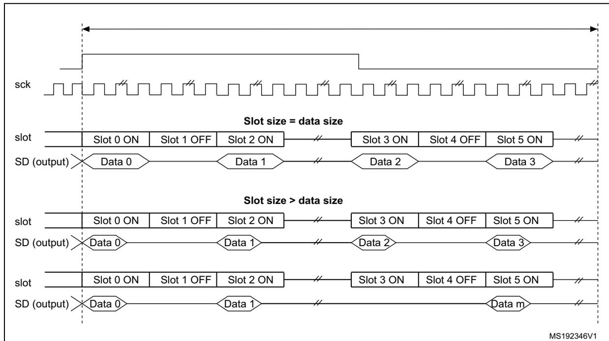
The diagram illustrates the timing of the SAI output data line (SD) and slot states (Slot 0 ON, Slot 1 OFF, Slot 2 ON, etc.) for two cases: Slot size = data size and Slot size > data size. The SCK signal is shown at the top. The SD (output) line is shown below the slot states. In the first case (Slot size = data size), the SD line is driven with Data 0, Data 1, Data 2, and Data 3. In the second case (Slot size > data size), the SD line is driven with Data 0, Data 1, Data 2, Data 3, and Data m. The diagram also shows the slot states for each case, with Slot 0 ON, Slot 1 OFF, Slot 2 ON, Slot 3 ON, Slot 4 OFF, and Slot 5 ON. The diagram is labeled MS192346V1.
If the TRIS bit in the SAI_xCR2 register is cleared, all the High impedance states on the SD output line on Figure 360 and Figure 361 are replaced by a drive with a value of 0.
30.13 Error flags
The SAI embeds some error flags:
- – FIFO overrun/underrun,
- – Anticipated frame synchronization detection,
- – Late frame synchronization detection,
- – Codec not ready (AC'97 exclusively),
- – Wrong clock configuration in master mode.
30.13.1 FIFO overrun/underrun (OVRUDR)
The FIFO Overrun/Underrun bit is called OVRUDR in the SAI_xSR register.
The overrun or underrun errors occupy the same bit since an audio block can be either receiver or transmitter and each audio block in an SAI has its own SAI_xSR register.
Overrun
When the audio block is configured as receiver, an overrun condition may appear if data is received in an audio frame when the FIFO is full and is not able to store the received data. In this case, the received data is lost, the flag OVRUDR in the SAI_xSR register is set and an interrupt is generated if bit OVRUDRIE is set in the SAI_xIM register. The slot number from which the overrun occurs, is stored internally. No more data will be stored into the FIFO until it becomes free to store new data. When the FIFO has at least one data free, the SAI audio block receiver will store new data (from new audio frame) from the slot number which
was stored internally when the overrun condition was detected, and this, to avoid data slot de-alignment in the destination memory (refer to Figure 362 ).
The OVRUDR flag is cleared when bit COVRUDR is set in the SAI_xCLRFR register.
Figure 362. Overrun detection error
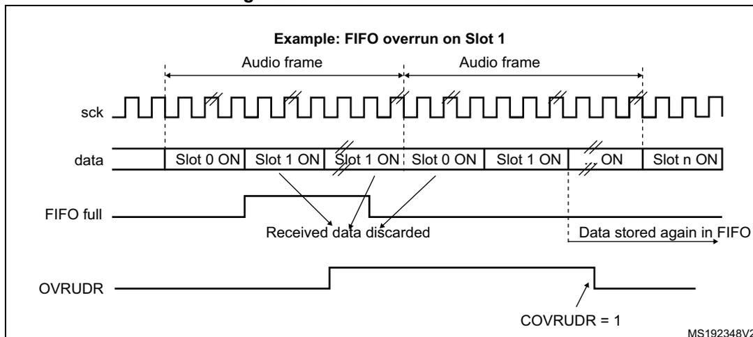
The diagram illustrates an overrun condition in the SAI. It shows the SCK signal, the data slots (Slot 0 ON, Slot 1 ON, Slot 1 ON, Slot 0 ON, Slot 1 ON, ON, Slot n ON), the FIFO level, and the OVRUDR flag. The FIFO level rises when data is received and falls when data is transmitted. The OVRUDR flag goes high when the FIFO is full and data is received, and goes low when the FIFO is empty and data is transmitted. The text 'Received data discarded' is shown when the FIFO is full and data is received. The text 'Data stored again in FIFO' is shown when the FIFO is empty and data is received. The text 'COVRUDR = 1' is shown when the OVRUDR flag is high.
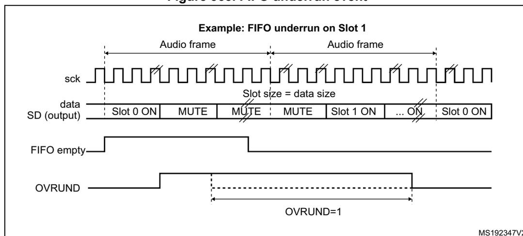
Underrun
An underrun may occur when the audio block in the SAI is a transmitter and the FIFO is empty when data needs to be transmitted (the audio block configuration (Master or Slave) is not relevant). If an underrun is detected, the software must resynchronize data and slot. Proceed as follows:
- 1. Disable the SAI peripheral by resetting the SAIEN bit of the SAI_xCR1 register. Check that the SAI has been disabled by reading back the SAIEN bit (SAIEN should be equal to 0).
- 2. Flush the Tx FIFO through the FFLUS bit of the SAI_xCR2 register.
- 3. Re-assigned to the correct data to be transferred on the first active slot of the new frame.
- 4. Re-enabling the SAI peripheral (SAIEN bit set to 1).
The underrun event sets the OVRUDR flag in the SAI_xSR register and an interrupt is generated if the OVRUDRIE bit is set in the SAI_xIM register. To clear this flag, set the COVRUDR bit in the SAI_xCLRFR register.
Figure 363. FIFO underrun event
30.13.2 Anticipated frame synchronisation detection (AFSDET)
This flag AFSDET is used only in Slave mode. In master mode, it is never asserted. It informs about the detection of a frame synchronisation (FS) earlier than expected since the frame length, the frame polarity, the frame offset are defined and known.
Early detection sets flag AFSDET in the SAI_xSR register.
This detection has no effect on the current audio frame which is not sensitive to the anticipated FS. This means that “parasitic” events on signal FS are flagged without any perturbation of the current audio frame.
If bit AFSDETIE is set in the SAI_xIM register, an interrupt is generated. To clear the flag AFSDET, bit CAFSDET in the SAI_xCLRFR register has to be set.
To resynchronize with the master after Anticipated frame detection error, four steps should be respected:
- 1. SAI block should be disabled by resetting SAIEN bit in SAI_xCR1 register, to be sure that the SAI is disabled SAIEN bit should be equal to 0 (reading back this bit).
- 2. FIFO should be flushed via FFLUS bit in SAI_xCR2 register.
- 3. Re-enabling the SAI peripheral (SAIEN bit set to 1) then the SAI.
- 4. SAI block will wait for the assertion on FS to restart the synchronization with master.
Note: This flag is not asserted in AC'97 since the SAI audio block acts as a link controller and generates the FS signal even when declared as slave.
30.13.3 Late frame synchronization detection
Flag LFSDET in the SAI_xSR register can be set only when the SAI audio block is defined as slave. The frame length, the frame polarity and the frame offset configuration are known in register SAI_xFRCR.
If the external master does not send the FS signal at the expecting time (generating the signal too late), the flag LFSDET in the SAI_xSR register will be set and an interrupt is generated if bit LFSDETIE in the SAI_xIM register is set.
The flag is cleared when bit CLFSDET is set in the SAI_xCLRFR register.
The late frame synchronisation detection flag is set when the error is detected, SAI needs to be resynchronized with the master (the four steps described above should be respected).
This detection and flag assertion can detect glitches on the SCK clock in a noisy environment, detected by the state machine of the audio block. It could incorrectly shift the SAI audio block state machine from one state in the current audio frame, thus corrupting the frame.
There is no corruption if the external master is not managing the audio data frame transfer in a continuous mode, which should not be the case for most application purposes. In this case, flag LFSDDET will be set.
Note: This flag is not asserted in AC'97 mode since the SAI audio block acts as a link controller and generates the FS signal even when declared as slave.
30.13.4 Codec not ready (CNRDY AC'97)
The flag CNRDY in the SAI_xSR register is relevant only if the SAI audio block is configured to work in AC'97 mode (bit PRTCFCFG[1:0] = 10 in the SAI_xCR1 register). If bit CNRDYIE is set in the SAI_xIM register, an interrupt will be generated when the flag CNRDY is set.
It is asserted when the codec is not ready to communicate during the reception of the TAG 0 (slot0) of the AC'97 audio frame. In this case, there will be no data automatically stored into the FIFO since the codec is not ready, until the TAG 0 indicates that the codec is ready. All the active slots defined in the SAI_xSLOTR register will be captured when the codec is ready.
To clear the flag, bit CCNRDY in the SAI_xCLRFR register has to be set.
30.13.5 Wrong clock configuration in master mode (with NODIV = 0)
When the audio block is master (MODE[1] = 0 in the SAI_xCR1 register) and if bit NODIV in the SAI_xCR1 is clear, the flag WCKCFG will be set if bit FRL[7:0] in the SAI_xFRCR is not set with a proper value when the SAIxEN bit in the SAI_xCR1 register is set, in order to respect this following rule:
where n is in the range from 3 to 8.
If bit WCKCFGIE is set, an interrupt is generated when flag WCKCFG is set in the SAI_xSR register. To clear the flag, set bit CWCKCFG bit in the SAI_xCLRFR register.
When bit WCKCFG is set, the audio block is automatically disabled, clearing bit SAIxEN in the SAI_xCR1 register via hardware.
The above formula is intended to guarantee that the number of MCLK pulses by bit clock is an even integer in the audio frame with a 50% duty cycle bit clock generation to guarantee the good quality of the audio sounds or acquisitions.
30.14 Interrupt sources
The SAI has 7 possible interrupt sources as illustrated by Table 184 .
Table 184. Interrupt sources
| Interrupt source | Interrupt group | Audio block mode | Interrupt enable | Interrupt clear |
|---|---|---|---|---|
| FREQ | FREQ | Master or Slave Receiver or transmitter | FREQIE in SAI_xIM register | Depend on: - FIFO threshold setting (FLTH bits in SAI_CR2) - Communication direction transmitter or receiver for more details please refer to Internal FIFOs section |
| OVRUDR | ERROR | Master or Slave Receiver or transmitter | OVRUDRIE in SAI_xIM register | COVRUDR = 1 in SAI_xCLRFR register |
| AFSDET | ERROR | Slave (Not used in AC'97 mode) | AFSDETIE in SAI_xIM register | CAFSDET = 1 in SAI_xCLRFR register |
| LFSDET | ERROR | Slave (Not used in AC'97 mode) | LFSDETIE in SAI_xIM register | CLFSDET = 1 in SAI_xCLRFR register |
| CNRDY | ERROR | Slave (Only in AC'97 mode) | CNRDYIE in SAI_xIM register | CCNRDY = 1 in SAI_xCLRFR register |
| MUTEDET | MUTE | Master or slave Receiver mode only | MUTEDETIE in SAI_xIM register | CMUTEDET = 1 in SAI_xCLRFR register |
| WCKCFG | ERROR | Master with NODIV = 0 in the SAI_xCR1 register | WCKCFGIE in SAI_xIM register | CWCKCFG = 1 in SAI_xCLRFR register |
Below are the SAI configuration steps to follow when an interrupt occurs:
- 1. Disable SAI interrupt.
- 2. Configure SAI.
- 3. Configure SAI interrupt source.
- 4. Enable SAI.
30.15 Disabling the SAI
The audio block in the SAI can be disabled at any moment by clearing bit SAIxEN in the SAI_xCR1 register. All the frames that have already started will be automatically completed before the total extinction of the SAI. Bit SAIxEN in the SAI_xCR1 register will stay high until the SAI is completely switched-off at the end of the current audio frame transfer.
If there is an audio block in the SAI synchronous with the other one, the one which is the master must be disabled first.
30.16 SAI DMA interface
In order to free the CPU and to optimize the bus bandwidth, each SAI audio block has an independent DMA interface in order to read or to write into the SAI_xDR register (to hit the internal FIFO). There is one DMA channel per audio block following basic DMA request/acknowledge protocol.
To configure the audio block to transfer through the DMA interface, set bit DMAEN in the SAI_xCR1 register. The DMA request is managed directly by the FIFO controller depend of FIFO threshold level (for more details please refer to Internal FIFOs section). DMA direction is linked to the SAI audio block configuration:
- • If the audio block is a transmitter, the audio block's FIFO controller outputs a DMA request to load the FIFO with data written in the SAI_xDR register.
- • If the audio block is a receiver, the DMA request will concern read operations from the SAI_xDR register.
Below are the SAI configuration steps followed when DMA is used:
- 1. Configure SAI and FIFO Threshold level (in order to specify when the DMA request to be launched)
- 2. Configure SAI DMA channel
- 3. Enable DMA
- 4. Enable SAI
Note: Before configuring the SAI block, the SAI DMA channel must be disabled.
30.17 SAI registers
30.17.1 SAI xConfiguration register 1 (SAI_xCR1) where x is A or B
Address offset: Block A: 0x004
Address offset: Block B: 0x024
Reset value: 0x0000 0040
| 31 | 30 | 29 | 28 | 27 | 26 | 25 | 24 | 23 | 22 | 21 | 20 | 19 | 18 | 17 | 16 |
|---|---|---|---|---|---|---|---|---|---|---|---|---|---|---|---|
| Reserved | MCKDIV[3:0] | NODIV | Res. | DMAEN | SAIxEN | ||||||||||
| rw | rw | rw | rw | rw | rw | rw | |||||||||
| 15 | 14 | 13 | 12 | 11 | 10 | 9 | 8 | 7 | 6 | 5 | 4 | 3 | 2 | 1 | 0 |
|---|---|---|---|---|---|---|---|---|---|---|---|---|---|---|---|
| Reserved | OUTDRIV | MONO | SYNCEN[1:0] | CKSTR | LSBFIRST | DS[2:0] | Res. | PRTCFG[1:0] | MODE[1:0] | ||||||
| rw | rw | rw | rw | rw | rw | rw | rw | rw | rw | rw | rw | ||||
Bits 31:24 Reserved, always read as 0.
Bit 23:20 MCKDIV[3:0] : Master clock divider. These bits are set and cleared by software.
- 0000: Divides by 1 the master clock input.
Otherwise, The Master clock frequency is calculated accordingly to the following formula:
These bits have no meaning when the audio block is slave.
They have to be configured when the audio block is disabled.
Bit 19 NODIV : No divider. This bit is set and cleared by software.
- 0: Master Clock divider is enabled
- 1: No divider used in the clock generator (in this case Master Clock Divider bit has no effect)
Bit 18 Reserved, always read as 0.
Bit 17 DMAEN : DMA enable. This bit is set and cleared by software.
- 0: DMA is disabled
- 1: DMA is enabled
Note: In receiver mode, the bits MODE must be configured before setting bit DMAEN to avoid a DMA request since the audio block is transmitter after reset (default setting)
Bit 16 SAIxEN : Audio block enable where x is A or B. This bit is set by software. It is cleared by hardware, after disabling it by software (writing the bit low), the audio is completely disabled (waiting for the end of the current frame).
- 0: Audio block is disabled
- 1: Audio block is enabled: this bit can be set only if it is at 0 during the write operation (means the SAI is completely disabled before being re-enabled).
This bit allows to control the state of the audio block. If it is disabled somewhere in an audio frame, the on-going transfer will be completed and the cell will be totally disabled at the end of this audio frame transfer.
Note: When SAIx block is configured as master mode, clock must be present on the input of the SAI before setting SAIxEN bit.
Bits 15:14 Reserved, always read as 0.
Bit 13 OUTDRIV : Output drive. This bit is set and cleared by software.
- 0: Audio block output driven when SAIEN is set
- 1: Audio block output driven immediately after the setting of this bit.
Note: This bit has to be set before enabling the audio block but after the audio block configuration.
Bit 12 MONO : Mono mode. This bit is set and cleared by software.
0: Stereo mode
1: Mono mode.
This bit has a meaning only when the number of slots is equal to 2.
When the Mono mode is selected, the data of the slot 0 data is duplicated on the slot 1 when the audio block is a transmitter. In reception mode, the slot1 is discarded and only the data received from the slot 0 will be stored.
Refer to Section 30.12.2 for more details.
Bits 11:10 SYNCPOL[1:0] : Synchronization enable. This bit is set and cleared by software.
00: audio block is asynchronous.
01: audio block is synchronous with the other internal audio block. In this case audio block should be configured in Slave mode
10: Reserved.
11: Not used
These bits have to be configured when the audio block is disabled.
Bit 9 CKSTR : Clock strobing edge. This bit is set and cleared by software.
0: data strobing edge is falling edge of SCK
1: data strobing edge is rising edge of SCK
This bit has to be configured when the audio block is disabled.
Bit 8 LSBFIRST : Least significant bit first. This bit is set and cleared by software.
0: data is transferred with the MSB of the data first
1: data is transferred with the LSB of the data first
This bit has to be configured when the audio block is disabled.
This bit has no meaning in AC'97 audio protocol since in AC'97 data is transferred with the MSB of the data first.
Bits 7:5 DS[2:0] : Data size. These bits are set and cleared by software.
000: Not used
001: Not used
010: 8-bit
011: 10-bit
100: 16-bit
101: 20-bit
110: 24-bit
111: 32-bit
When the companding mode is selected (bit COMP[1:0]), these DS[1:0] are ignored since the data size is fixed to 8-bit mode by the algorithm itself.
These bits must be configured when the audio block is disabled.
Note: When AC'97 mode is selected the data sizes that can be used are: 16-bit or 20-bit only, else SAI behavior is not guaranteed.
Bit 4 Reserved, always read as 0.
Bits 3:2 PRTCFG[1:0] : Protocol configuration. These bits are set and cleared by software.
00: Free protocol
01: Not used
10: AC'97 protocol
11: Not used
Free protocol selection allows to use the powerful configuration of the audio block to address a specific audio protocol (like I2S, LSB/MSB justified, TDM, PCM/DSP...) setting most of the configuration register bits as well as frame configuration register.
These bits have to be configured when the audio block is disabled.
Bits 1:0 MODE[1:0] : Audio block mode. These bits are set and cleared by software.
00: Master transmitter
01: Master receiver
10: Slave transmitter
11: Slave receiver
These bits have to be configured when the audio block is disabled.
Note: In Master transmitter mode the audio block will start to generate the FS and clocks
30.17.2 SAI xConfiguration register 2 (SAI_xCR2) where x is A or B
Address offset: Block A: 0x008
Address offset: Block B: 0x028
Reset value: 0x0000 0000
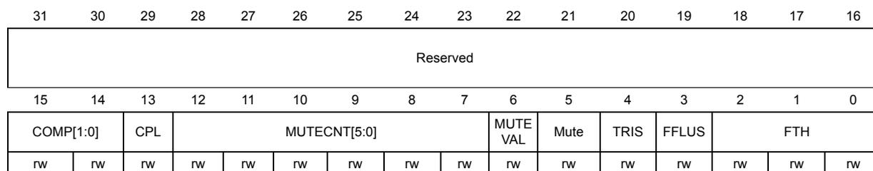
| 31 | 30 | 29 | 28 | 27 | 26 | 25 | 24 | 23 | 22 | 21 | 20 | 19 | 18 | 17 | 16 |
| Reserved | |||||||||||||||
| 15 | 14 | 13 | 12 | 11 | 10 | 9 | 8 | 7 | 6 | 5 | 4 | 3 | 2 | 1 | 0 |
| COMP[1:0] | CPL | MUTECNT[5:0] | MUTE VAL | Mute | TRIS | FFLUS | FTH | ||||||||
| rw | rw | rw | rw | rw | rw | rw | rw | rw | rw | rw | rw | rw | rw | rw | rw |
Bits 31:16 Reserved, always read as 0
Bits 15:14 COMP[1:0] : Companding mode. These bits are set and cleared by software.
00: No companding algorithm
01: Reserved.
10: \( \mu \) -Law algorithm
11: A-Law algorithm
The \( \mu \) -Law and the A-Law log are a part of the CCITT G.711 recommendation, the type of complement that will be used depends on ComPLement bit .
The data expansion or data compression are determined by the state of bit MODE[0].
The data compression is applied if the audio block is configured as a transmitter.
The data expansion is automatically applied when the audio block is configured as a receiver.
Refer to Section 30.12.3 for more details.
Note: Companding mode is applicable only when TDM is selected.
Bit 13 CPL : Complement bit. This bit is set and cleared by software.
It defines the type of complement to be used for companding mode
0: 1's complement representation.
1: 2's complement representation.
Note: This bit has effect only when the companding mode is \( \mu \) -Law algorithm or A-Law algorithm.
Bits 12:7 MUTECNT[5:0] : Mute counter. These bits are set and cleared by software.
These bits are used only in reception mode.
The value set in these bits is compared to the number of consecutive mute frames detected in reception. When the number of mute frames is equal to this value, the flag MUTEDET will be set and an interrupt will be generated if bit MUTEDETIE is set.
Refer to Section 30.12.1 for more details.
Bit 6 MUTEVAL : Mute value. This bit is set and cleared by software. This bit has to be written before enabling the audio block: SAIxEN.
0: Bit value 0 is sent during the MUTE mode.
1: Last values are sent during the MUTE mode.
This bit has a meaning only when the audio block is a transmitter and when the number of slots is lower or equal to 2 and if the MUTE bit is set.
If more slots are declared, the bit value sent during the transmission in mute mode will be equal to 0, whatever the value of this MUTEVAL bit.
If the number of slot is lower or equal to 2 and MUTEVAL = 1, the mute value transmitted for each slot will be the ones sent during the previous frame.
Refer to Section 30.12.1 for more details.
Bit 5 MUTE : Mute. This bit is set and cleared by software.
0: No Mute mode.
1: Mute mode enabled.
This bit has a meaning only when the audio block is a transmitter. The MUTE value is linked to the MUTEVAL value if the number of slots is lower or equal to 2, or equal to 0 if it is greater than 2.
Refer to Section 30.12.1 for more details.
Bit 4 TRIS : Tristate management on data line. This bit is set and cleared by software.
0: SD output line is still driven by the SAI when a slot is inactive.
1: SD output line is released (HI-Z) at the end of the last data bit of the last active slot if the next one is inactive.
This bit has a meaning only if the audio block is configured to be a transmitter.
This bit should be configured when SAI is disabled.
Refer to Section 30.12.4 for more details.
Bit 3 FFLUSH : FIFO flush. This bit is set by software. It is always read low.
0: No FIFO flush.
1: FIFO flush.
Writing 1 to the bit triggers the FIFO Flush. All the internal FIFO pointers (read and write) are cleared.
Data still present in the FIFO will be lost in such case (no more transmission or received data lost).
This bit should be configured when SAI is disabled.
Before flushing SAI, DMA stream/interruption must be disabled
Bits 2:0 FTH : FIFO threshold. This bit is set and cleared by software.
000: FIFO empty
001: ¼ FIFO
010: ½ FIFO
011: ¾ FIFO
100: FIFO full
101: Reserved
110: Reserved
111: Reserved
30.17.3 SAI xFrame configuration register (SAI_XFCR) where x is A or B
Address offset: Block A: 0x00C
Address offset: Block B: 0x02C
Reset value: 0x0000 0007
Note: This register has no meaning in AC'97 audio protocol
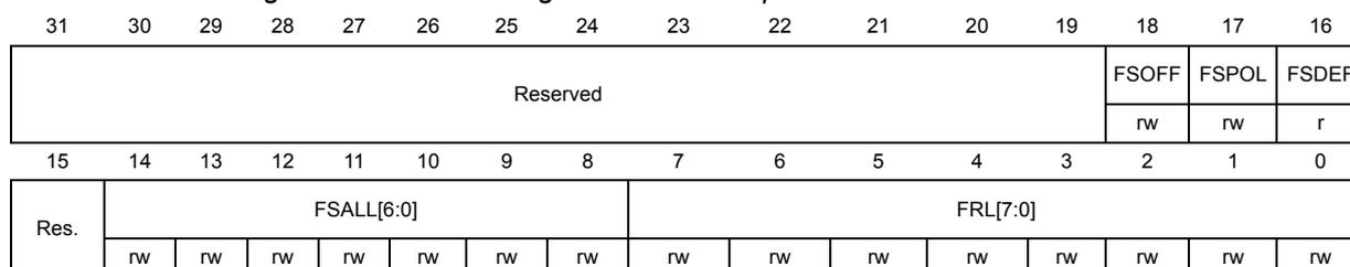
| 31 | 30 | 29 | 28 | 27 | 26 | 25 | 24 | 23 | 22 | 21 | 20 | 19 | 18 | 17 | 16 |
| Reserved | FSOFF | FSPOL | FSDEF | ||||||||||||
| r/w | r/w | r | |||||||||||||
| 15 | 14 | 13 | 12 | 11 | 10 | 9 | 8 | 7 | 6 | 5 | 4 | 3 | 2 | 1 | 0 |
| Res. | FSALL[6:0] | FRL[7:0] | |||||||||||||
| r/w | r/w | r/w | r/w | r/w | r/w | r/w | r/w | r/w | r/w | r/w | r/w | r/w | r/w | r/w | |
Bits 31:19 Reserved, always read as 0.
Bit 18 FSOFF : Frame synchronization offset. This bit is set and cleared by software.
0: FS is asserted on the first bit of the slot 0.
1: FS is asserted one bit before the first bit of the slot 0.
This bit has no meaning and is not used in AC'97 audio block configuration.
This bit must be configured when the audio block is disabled.
Bit 17 FSPOL : Frame synchronization polarity. This bit is set and cleared by software
0: FS is active low (falling edge)
1: FS is active high (rising edge)
This bit is used to configure the level of the start of frame on the FS signal.
This bit has no meaning and is not used in AC'97 audio block configuration.
This bit must be configured when the audio block is disabled.
Bit 16 FSDEF : Frame synchronization definition. This bit is set and cleared by software.
0: FS signal is a start frame signal
1: FS signal is a start of frame signal + channel side identification
When the bit is set, the number of slots defined in the SAI_ASLOTR register has to be even. It means that there will be half of this number of slots dedicated for the left channel and the other slots for the right channel (e.g: this bit has to be set for I2S or MSB/LSB-justified protocols...)
This bit has no meaning and is not used in AC'97 audio block configuration.
This bit must be configured when the audio block is disabled.
Bit 15 Reserved, always read as 0.
Bits 14:8 FSALL[6:0] : Frame synchronization active level length. These bits are set and cleared by software
The value set in these bits specifies the length in number of bit clock (SCK) + 1 (FSALL[6:0] + 1) of the active level of the FS signal in the audio frame
These bits have no meaning and are not used in AC'97 audio block configuration.
These bits must be configured when the audio block is disabled.
Bits 7:0 FRL[7:0] : Frame length. These bits are set and cleared by software.
They define the length of the audio frame. More precisely, these bits define the number of SCK clocks for each audio frame.
The number of bits in the frame is equal to FRL[7:0] + 1.
The minimum number of bits to transfer in an audio frame has to be equal to 8 or else the audio block will have unexpected behavior. This is the case when the data size is 8-bit and only one slot 0 is defined in NBSLOT[4:0] in the SAI_ASLOTR register (NBSLOT[3:0] = 0000).
In master mode, if the master clock MCLK_x pin is declared as an output, the frame length should be aligned to a number equal to a power of 2, from 8 to 256 in order to keep in an audio frame, an integer number of MCLK pulses by bit clock for correct operation for external DAC/ADC inside the decoders.
The frame length should be even.
These bits have no meaning and are not used in AC'97 audio block configuration. They must be configured when the audio block is disabled.
30.17.4 SAI xSlot register (SAI_xSLOTR) where x is A or B
Address offset: Block A: 0x010
Address offset: Block B: 0x030
Reset value: 0x0000 0000
Note: This register has no meaning in AC'97 audio protocol
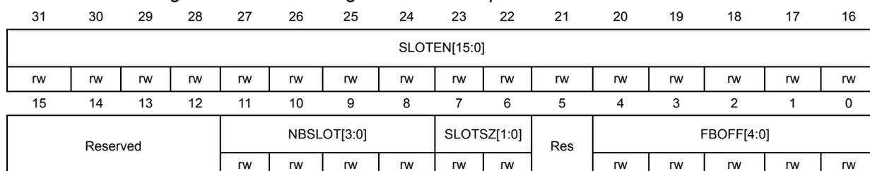
| 31 | 30 | 29 | 28 | 27 | 26 | 25 | 24 | 23 | 22 | 21 | 20 | 19 | 18 | 17 | 16 |
| SLOTEN[15:0] | |||||||||||||||
| rw | rw | rw | rw | rw | rw | rw | rw | rw | rw | rw | rw | rw | rw | rw | rw |
| 15 | 14 | 13 | 12 | 11 | 10 | 9 | 8 | 7 | 6 | 5 | 4 | 3 | 2 | 1 | 0 |
| Reserved | NBSLOT[3:0] | SLOTSZ[1:0] | Res | FBOFF[4:0] | |||||||||||
| rw | rw | rw | rw | rw | rw | rw | rw | rw | rw | rw | |||||
Bits 31:16 SLOTEN[15:0] : Slot enable. These bits are set and cleared by software.
Each bit of the SLOTEN bits identify a slot position from 0 to 15 (maximum 16 slots)
0: Inactive slot.
1: Active slot.
These bits must be set when the audio block is disabled.
They are ignored in AC'97 mode.
Bits 15:12 Reserved, always read as 0.
Bits 11:8 NBSLOT[3:0] : Number of slots in an audio frame. These bits are set and cleared by software.
The value set in these bits register represents the number of slots + 1 in the audio frame (including the number of inactive slots). The maximum number of slots is 16.
The number of slots should be even if bit FSDEF in the SAI_AFRCR register is set.
If the size is greater than the data size, the remaining bits will be forced to 0 if bit TRIS in the SAI_xCR1 register is clear, otherwise they will be forced to 0 if the next slot is active or the SD line will be forced to HI-Z if the next slot is inactive and bit TRIS = 1.
These bits must be set when the audio block is disabled.
They are ignored in AC'97 mode.
Bits 7:6 SLOTSZ[1:0] : Slot size
This bits is set and cleared by software.
00: The slot size is equivalent to the data size (specified in DS[3:0] in the SAI_ACR1 register).
01: 16-bit
10: 32-bit
11: Reserved
The slot size must be greater or equal to the data size. If this condition is not respected, the behavior of the SAI will be undetermined.
These bits must be set when the audio block is disabled.
They are ignored in AC'97 mode.
Bit 1 Reserved, always read as 0.
Bits 4:0 FBOFF[4:0] : First bit offset
These bits are set and cleared by software.
The value set in these bits represents the position of the first data transfer bit in the slot. It represents an offset value. During this offset phase 0 value are sent on the data line for transmission mode. For reception mode, the received bit are discarded during the offset phase.
These bits must be set when the audio block is disabled.
They are ignored in AC'97 mode.
30.17.5 SAI xInterrupt mask register2(SAI_xIM) where x is A or B
Address offset: blockA: 0x014
Address offset: block B: 0x034
Reset value: 0x0000 0000
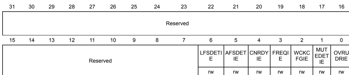
| 31 | 30 | 29 | 28 | 27 | 26 | 25 | 24 | 23 | 22 | 21 | 20 | 19 | 18 | 17 | 16 |
| Reserved | |||||||||||||||
| 15 | 14 | 13 | 12 | 11 | 10 | 9 | 8 | 7 | 6 | 5 | 4 | 3 | 2 | 1 | 0 |
| Reserved | LFSDETI E | AFSDETI IE | CNRDY IE | FREQI E | WCKC FGIE | MUT EDETI IE | OVRU DRIE | ||||||||
| rw | rw | rw | rw | rw | rw | rw | |||||||||
Bits 31:7 Reserved, always read as 0.
Bit 6 LFSDETIE : Late frame synchronization detection interrupt enable. This bit is set and cleared by software.
0: Interrupt is disabled
1: Interrupt is enabled
When this bit is set, an interrupt will be generated if the LFSDET bit is set in the SAI_ASR register.
This bit has no meaning in AC'97 mode. It has no meaning also if the audio block is master.
Bit 5 AFSDETIE : Anticipated frame synchronization detection interrupt enable. This bit is set and cleared by software.
0: Interrupt is disabled
1: Interrupt is enabled
When this bit is set, an interrupt will be generated if the AFSDET bit in the SAI_ASR register is set.
This bit has no meaning in AC'97 mode. It has no meaning also if the audio block is master.
Bit 4 CNRDYIE : Codec not ready interrupt enable (ac'97). This bit is set and cleared by software.
0: Interrupt is disabled
1: Interrupt is enabled
When the interrupt is enabled, the audio block will detect in the slot 0 (tag0) of the AC'97 frame if the codec connected on this line is ready or not. If not, the flag CNRDY in the SAI_ASR register will be set and an interruption will be generated.
This bit has a meaning only if the AC'97 mode is selected (bit PRTCFCFG[1:0]) and the audio block is a receiver.
Bit 3 FREQIE : FIFO request interrupt enable. This bit is set and cleared by software.
0: Interrupt is disabled
1: Interrupt is enabled
When this bit is set, an interrupt will be generated if the FREQ bit in the SAI_ASR register is set.
In receiver mode, the bit MODE must be configured before setting bit FREQIE to avoid a parasitic interruption since the audio block is a transmitter (default setting).
Bit 2 WCKCFGIE : Wrong clock configuration interrupt enable. This bit is set and cleared by software.
0: Interrupt is disabled
1: Interrupt is enabled
This bit is considered only if the audio block is configured as master (MODE[1] = 0 in the SAI_ACR1 register) and bit NODIV = 0 in the SAI_xCR1 register.
It generates an interrupt if the flag WCKCFG in the SAI_ASR register is set.
Note: This bit is used only in TDM mode and has no meaning for other modes.
Bit 1 MUTEDETIE : Mute detection interrupt enable. This bit is set and cleared by software.
0: Interrupt is disabled
1: Interrupt is enabled
When this bit is set, an interrupt will be generated if the MUTEDET bit in the SAI_ASR register is set.
This bit has a meaning only if the audio block is configured in receiver mode.
Bit 0 OVRUDRIE : Overrun/underrun interrupt enable. This bit is set and cleared by software.
0: Interrupt is disabled
1: Interrupt is enabled
When this bit is set, an interrupt will be generated if the OVRUDR bit in the SAI_ASR register is set.
30.17.6 SAI xStatus register (SAI_xSR) where x is A or B
Address offset: block A: 0x018
Address offset: block B: 0x038
Reset value: 0x0000 0008
| 31 | 30 | 29 | 28 | 27 | 26 | 25 | 24 | 23 | 22 | 21 | 20 | 19 | 18 | 17 | 16 |
|---|---|---|---|---|---|---|---|---|---|---|---|---|---|---|---|
| Reserved | FLTH | ||||||||||||||
| r | r | r | |||||||||||||
| 15 | 14 | 13 | 12 | 11 | 10 | 9 | 8 | 7 | 6 | 5 | 4 | 3 | 2 | 1 | 0 |
| Reserved | LFSDET | AFSDET | CNRDY | FREQ | WCKCFG | MUTEDET | OVRUDR | ||||||||
| r | r | r | r | r | r | r | |||||||||
Bits 31:19 Reserved, always read as 0.
Bits 18:16 FLTH : FIFO level threshold. This bit is read only. The FIFO level threshold flag is managed only by hardware and its setting depends on SAI block configuration (transmitter or receiver mode).
If SAI block is configured as transmitter:
- 000: FIFO_empty
- 001: FIFO <= 1/4 but not empty
- 010: 1/4 < FIFO <= 1/2
- 011: 1/2 < FIFO <= 3/4
- 100: 3/4 < FIFO but not full
- 101: FIFO full
If SAI block is configured as receiver:
- 000: FIFO_empty
- 001: FIFO < 1/4 but not empty
- 010: 1/4 <= FIFO < 1/2
- 011: 1/2 <= FIFO < 3/4
- 100: 3/4 <= FIFO but not full
- 101: FIFO full
Bits 15:7 Reserved, always read as 0.
Bit 6 LFSDET : Late frame synchronization detection. This bit is read only.
- 0: No error.
- 1: Frame synchronization signal is not present at the right time.
This flag can be set only if the audio block is configured in Slave mode.
It is not used in AC'97 mode.
It may generate an interrupt if bit LFSDETIE in the
SAI_xIM
register is set.
This flag is cleared when the software sets bit CLFSDET in the
SAI_xCLRFR
register
Bit 5 AFSDET : Anticipated frame synchronization detection. This bit is read only.
- 0: No error.
- 1: Frame synchronization signal is detected earlier than expected.
This flag can be set only if the audio block is configured in Slave mode.
It is not used in AC'97.
It may generate an interrupt if bit AFSDETIE in the
SAI_xIM
register is set.
This flag is cleared when the software sets bit CAFSDET in the
SAI_xCLRFR
register
Bit 4 CNRDY : Codec not ready. This bit is read only.
0: The external AC'97 codec is ready
1: The external AC'97 codec is not ready
This bit is used only when the AC'97 audio protocol is selected in the SAI_xCR1 register and is configured in receiver mode.
It may generate an interrupt if bit CNRDYIE in the SAI_xIM register is set.
This flag is cleared when the software sets bit CCNRDY in the SAI_xCLRFR register
Bit 3 FREQ : FIFO request. This bit is read only.
0: No FIFO request.
1: FIFO request to read or to write the SAI_xDR.
The request depends on the audio block configuration.
If configured in transmission, the FIFO request concerns a write request operation in the SAI_xDR.
If configured in reception, the FIFO request concerns a read request operation from the SAI_xDR.
This flag can generate an interrupt if bit FREQIE in the SAI_xIM register is set.
Bit 2 WCKCFG : Wrong clock configuration flag. This bit is read only.
0: The clock configuration is correct
1: The clock configuration does not respect the rule concerning the frame length specification defined in Section 30.7 (configuration of FRL[7:0] bit in the SAI_x_FRCR register)
This bit is used only when the audio block is master (MODE[1] = 0 in the SAI_xCR1 register) and when NODIV = 0 in the SAI_xCR1 register.
It may generate an interrupt if bit WCKCFGIE in the SAI_xIM register is set.
This flag is cleared when the software sets bit CWCKCFG in the SAI_xCLRFR register
Bit 1 MUTEDET : Mute detection. This bit is read only.
0: No MUTE detection on the SD input line
1: MUTE value detected on the SD input line (0 value) for a specified number of consecutive audio frame
This flag is set if consecutive 0 values are received in each slot of an audio frame and for a consecutive number of audio frames (set in the MUTECNT bit in the SAI_xCR2 register).
It may generate an interrupt if bit MUTEDETIE in the SAI_xIM register is set.
This flag is cleared when the software sets bit CMUTEDET in the SAI_xCLRFR register.
Bit 0 OVRUDR : Overrun / underrun. This bit is read only.
0: No overrun/underrun error.
1: Overrun/underrun error detection.
The overrun condition can occur only when the audio block is configured in reception.
The underrun condition can occur only when the audio block is configured in transmission.
It may generate an interrupt if bit OVRUDRIE in the SAI_xIM register is set.
This flag is cleared when the software set bit COVRUDR bit in the SAI_xCLRFR register.
30.17.7 SAI xClear flag register (SAI_xCLRFR) where X is A or B
Address offset: block A: 0x01C
Address offset: block B: 0x03C
Reset value: 0x0000 0000
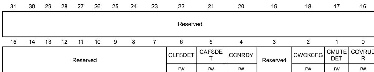
| 31 | 30 | 29 | 28 | 27 | 26 | 25 | 24 | 23 | 22 | 21 | 20 | 19 | 18 | 17 | 16 |
| Reserved | |||||||||||||||
| 15 | 14 | 13 | 12 | 11 | 10 | 9 | 8 | 7 | 6 | 5 | 4 | 3 | 2 | 1 | 0 |
| Reserved | CLFSDDET | CAFSDET | CCNRDY | Reserved | CWCKCFG | CMUTEDET | COVRUDR | ||||||||
| rw | rw | rw | rw | rw | rw | ||||||||||
Bits 31:7 Reserved, always read as 0.
Bit 6 CLFSDDET : Clear late frame synchronization detection flag. This bit is write only.
Writing 1 in this bit clears the flag LFSDDET in the SAI_xSR register.
It is not used in AC'97.
Reading this bit always returns the value 0.
Bit 5 CAFSDET : Clear anticipated frame synchronization detection flag. This bit is write only.
Writing 1 in this bit clears the flag AFSDDET in the SAI_xSR register.
It is not used in AC'97.
Reading this bit always returns the value 0.
Bit 4 CCNRDY : Clear codec not ready flag. This bit is write only.
Writing 1 in this bit clears the flag CNRDY in the SAI_xSR register.
This bit is used only when the AC'97 audio protocol is selected in the SAI_xCR1 register.
Reading this bit always returns the value 0.
Bit 3 Reserved, always read as 0.
Bit 2 CWCKCFG : Clear wrong clock configuration flag. This bit is write only.
Writing 1 in this bit clears the flag WCKCFG in the SAI_xSR register.
This bit is used only when the audio block is set as master (MODE[1] = 0 in the SAI_ACR1 register) and bit NODIV = 0 in the SAI_xCR1 register.
Reading this bit always returns the value 0.
Bit 1 CMUTEDET : Mute detection flag. This bit is write only.
Writing 1 in this bit clears the flag MUTEDDET in the SAI_xSR register.
Reading this bit always returns the value 0.
Bit 0 COVRUDR : Clear overrun / underrun. This bit is write only.
Writing 1 in this bit clears the flag OVRUDR in the SAI_xSR register.
Reading this bit always returns the value 0.
30.17.8 SAI xData register (SAI_xDR) where x is A or B
Address offset: block A: 0x020
Address offset: block B: 0x040
Reset value: 0x0000 0000
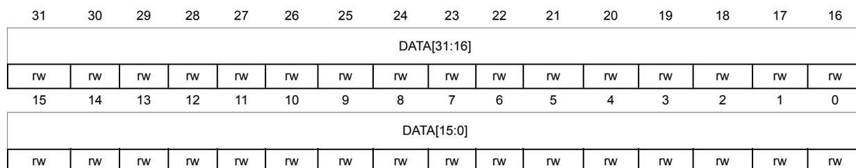
| 31 | 30 | 29 | 28 | 27 | 26 | 25 | 24 | 23 | 22 | 21 | 20 | 19 | 18 | 17 | 16 |
| DATA[31:16] | |||||||||||||||
| rw | rw | rw | rw | rw | rw | rw | rw | rw | rw | rw | rw | rw | rw | rw | rw |
| 15 | 14 | 13 | 12 | 11 | 10 | 9 | 8 | 7 | 6 | 5 | 4 | 3 | 2 | 1 | 0 |
| DATA[15:0] | |||||||||||||||
| rw | rw | rw | rw | rw | rw | rw | rw | rw | rw | rw | rw | rw | rw | rw | rw |
Bits 31:0 DATA[31:0] : Data
A write into this register has the effect of loading the FIFO if the FIFO is not full.
A read from this register has to effect of draining-up the FIFO if the FIFO is not empty.
30.17.9 SAI register map
The following table summarizes the SAI registers.
Table 185. SAI register map and reset values
| Offset | Register and reset value | 31 | 30 | 29 | 28 | 27 | 26 | 25 | 24 | 23 | 22 | 21 | 20 | 19 | 18 | 17 | 16 | 15 | 14 | 13 | 12 | 11 | 10 | 9 | 8 | 7 | 6 | 5 | 4 | 3 | 2 | 1 | 0 |
|---|---|---|---|---|---|---|---|---|---|---|---|---|---|---|---|---|---|---|---|---|---|---|---|---|---|---|---|---|---|---|---|---|---|
| 0x0004 or 0x0024 | SAI_xCR1 | Reserved | MCKDIV[3:0] | NODIV | Res. | DMAEN | SAIXEN | Reserved. | OutDri | MONO | SYNCEN[1:0] | CKSTR | LSBFIRST | DS[2:0] | Res. | PRTCFG[1:0] | MODE[1:0] | ||||||||||||||||
| Reset value | 0 | 0 | 0 | 0 | 0 | 0 | 0 | 0 | 0 | 0 | 0 | 0 | 0 | 0 | 1 | 0 | 0 | 0 | 0 | 0 | |||||||||||||
| 0x0008 or 0x0028 | SAI_xCR2 | Reserved | COMP[1:0] | CPL | MUTECN[5:0] | MUTEVAL | MUTE | TRIS | FFLUS | FTH | |||||||||||||||||||||||
| Reset value | 0 | 0 | 0 | 0 | 0 | 0 | 0 | 0 | 0 | 0 | 0 | 0 | 0 | 0 | 0 | 0 | |||||||||||||||||
| 0x000C or 0x002C | SAI_xFCR | Reserved | FSOFF | FSPOL | FSDEF | Reserved | FSALL[6:0] | FRL[7:0] | |||||||||||||||||||||||||
| Reset value | 0 | 0 | 0 | 0 | 0 | 0 | 0 | 0 | 0 | 0 | 0 | 0 | 0 | 0 | 0 | 1 | 1 | 1 | |||||||||||||||
| 0x0010 or 0x0030 | SAI_xSLOTR | SLOTEN[15:0] | Reserved | NBSLOT[3:0] | SLOTSZ[1:0] | Reserved | FBOFF[4:0] | ||||||||||||||||||||||||||
| Reset value | 0 | 0 | 0 | 0 | 0 | 0 | 0 | 0 | 0 | 0 | 0 | 0 | 0 | 0 | 0 | 0 | 0 | 0 | 0 | 0 | 0 | 0 | 0 | 0 | 0 | 0 | 0 | 0 | |||||
Table 185. SAI register map and reset values (continued)
| Offset | Register and reset value | 31 | 30 | 29 | 28 | 27 | 26 | 25 | 24 | 23 | 22 | 21 | 20 | 19 | 18 | 17 | 16 | 15 | 14 | 13 | 12 | 11 | 10 | 9 | 8 | 7 | 6 | 5 | 4 | 3 | 2 | 1 | 0 | |
|---|---|---|---|---|---|---|---|---|---|---|---|---|---|---|---|---|---|---|---|---|---|---|---|---|---|---|---|---|---|---|---|---|---|---|
| 0x0014 or 0x0034 | SAI_xIM | Reserved | LFSDET | AFSDETIE | CNRDYIE | FREQIE | WCKKCFG | MUTEDET | OVRUDRIE | |||||||||||||||||||||||||
| Reset value | 0 | 0 | 0 | 0 | 0 | 0 | 0 | |||||||||||||||||||||||||||
| 0x0018 or 0x0038 | SAI_xSR | Reserved | LFSDET | AFSDET | CNRDY | FREQ | WCKKCFG | MUTEDET | OVRUDR | |||||||||||||||||||||||||
| Reset value | 0 | 0 | 0 | 0 | 1 | 0 | 0 | |||||||||||||||||||||||||||
| 0x001C or 0x003C | SAI_xCLRF R | Reserved | LFSDET | CAFSDET | CNRDY | Res. | WCKKCFG | MUTEDET | OVRUDR | |||||||||||||||||||||||||
| Reset value | 0 | 0 | 0 | 0 | 0 | 0 | ||||||||||||||||||||||||||||
| 0x0020 or 0x0040 | SAI_xDR | DATA[31:0] | ||||||||||||||||||||||||||||||||
| Reset value | ||||||||||||||||||||||||||||||||||