4. Power controller (PWR)
4.1 Power supplies
The device requires a 1.8 to 3.6 V operating voltage supply ( \( V_{DD} \) ). An embedded linear voltage regulator is used to supply the internal 1.2 V digital power.
The real-time clock (RTC), the RTC backup registers, and the backup SRAM (BKP SRAM) can be powered from the \( V_{BAT} \) voltage when the main \( V_{DD} \) supply is powered off.
Note: Depending on the operating power supply range, some peripheral may be used with limited functionality and performance. For more details refer to section "General operating conditions" in STM32F76xxx and STM32F77xxx datasheets.
Figure 5. Power supply overview (STM32F769xx and STM32F779xx devices)
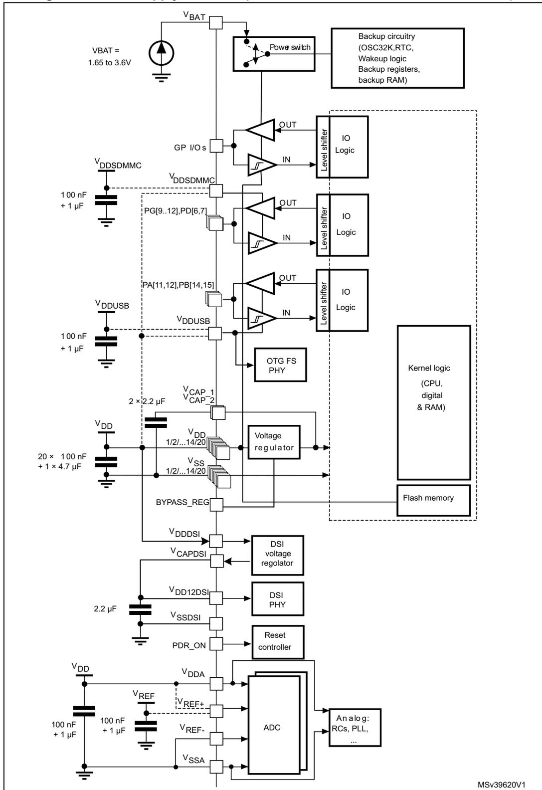
MSV39620V1
- 1. V DDA and V SSA must be connected to V DD and V SS , respectively.
4.1.1 Independent A/D converter supply and reference voltage
To improve conversion accuracy, the ADC has an independent power supply which can be separately filtered and shielded from noise on the PCB.
- • The ADC voltage supply input is available on a separate \( V_{DDA} \) pin.
- • An isolated supply ground connection is provided on pin \( V_{SSA} \) .
To ensure a better accuracy of low voltage inputs, the user can connect a separate external reference voltage ADC input on \( V_{REF} \) . The voltage on \( V_{REF} \) ranges from 1.8 V to \( V_{DDA} \) .
4.1.2 Independent USB transceivers supply
The \( V_{DDUSB} \) is an independent USB power supply for full speed transceivers (USB OTG FS and USB OTG HS in FS mode). It can be connected either to \( V_{DD} \) or an external independent power supply (3.0 to 3.6V) for USB transceivers (refer Figure 6 and Figure 7 ). For example, when the device is powered at 1.8V, an independent power supply 3.3V can be connected to \( V_{DDUSB} \) . When the \( V_{DDUSB} \) is connected to a separated power supply, it is independent from \( V_{DD} \) or \( V_{DDA} \) but it must be the last supply to be provided and the first to disappear. The following conditions \( V_{DDUSB} \) must be respected:
- • During power-on phase ( \( V_{DD} < V_{DD\_MIN} \) ), \( V_{DDUSB} \) should be always lower than \( V_{DD} \)
- • During power-down phase ( \( V_{DD} < V_{DD\_MIN} \) ), \( V_{DDUSB} \) should be always lower than \( V_{DD} \)
- • \( V_{DDUSB} \) rising and falling time rate specifications must be respected
- • In operating mode phase,
\(
V_{DDUSB}
\)
could be lower or higher than
\(
V_{DD}
\)
:
- – If USB (USB OTG_HS/OTG_FS) is used, the associated GPIOs powered by \( V_{DDUSB} \) are operating between \( V_{DDUSB\_MIN} \) and \( V_{DDUSB\_MAX} \) .
- – The \( V_{DDUSB} \) supplies both USB transceiver (USB OTG_HS and USB OTG_FS). If only one USB transceiver is used in the application, the GPIOs associated to the other USB transceiver are still supplied at by \( V_{DDUSB} \) .
- – If USB (USB OTG_HS/OTG_FS) is not used, the associated GPIOs powered by \( V_{DDUSB} \) are operating between \( V_{DD\_MIN} \) and \( V_{DD\_MAX} \) .
Figure 6. \( V_{DDUSB} \) connected to \( V_{DD} \) power supply
The diagram is a line graph plotting voltage (VDD) on the y-axis against time on the x-axis. The y-axis has two horizontal dotted reference lines labeled
\(
V_{DD\_MAX}
\)
and
\(
V_{DD\_MIN}
\)
. The x-axis is divided into three distinct time regions: "Power-on", "Operating mode", and "Power-down".
- In the "Power-on" phase, the voltage rises linearly from zero, crossing the
\(
V_{DD\_MIN}
\)
threshold until it reaches a plateau.
- In the "Operating mode" phase, the voltage remains constant at the plateau level. A label in this region states:
\(
V_{DD} = V_{DDA} = V_{DDUSB}
\)
.
- In the "Power-down" phase, the voltage decreases linearly from the plateau, crossing back below
\(
V_{DD\_MIN}
\)
to zero.
Vertical dashed lines mark the transitions between these phases at the points where the voltage curve intersects the
\(
V_{DD\_MIN}
\)
level. The reference number MS37591V1 is in the bottom right corner.
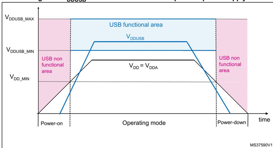
The graph shows the voltage levels over time for \( V_{DDUSB} \) and \( V_{DD} \) (which is equal to \( V_{DDA} \) ). The y-axis represents voltage levels: \( V_{DDUSB\_MAX} \) , \( V_{DDUSB\_MIN} \) , and \( V_{DD\_MIN} \) . The x-axis represents time, divided into three phases: Power-on, Operating mode, and Power-down. During the Power-on phase, both \( V_{DDUSB} \) and \( V_{DD} \) rise from 0V. \( V_{DDUSB} \) rises faster and reaches \( V_{DDUSB\_MAX} \) before \( V_{DD} \) reaches \( V_{DD\_MIN} \) . During the Operating mode, \( V_{DDUSB} \) is constant at \( V_{DDUSB\_MAX} \) and \( V_{DD} \) is constant at \( V_{DD\_MIN} \) . During the Power-down phase, both voltages fall. \( V_{DDUSB} \) falls faster than \( V_{DD} \) . The graph is divided into three regions: USB non functional area (pink) during power transitions, and USB functional area (blue) during the operating mode. The label MS37590V1 is present in the bottom right corner.
4.1.3 Independent SDMMC2 supply
The \( V_{DDSDMMC} \) is an independent power supply for SDMMC2 peripheral IOs (PD6, PD7, PG9..12). It can be connected either to \( V_{DD} \) or an external independent power supply.
For example, when the device is powered at 1.8V, an independent power supply 3.3V can be connected to \( V_{DDSDMMC} \) . When the \( V_{DDSDMMC} \) is connected to a separated power supply, it is independent from \( V_{DD} \) and \( V_{DDA} \) but it must be the last supply to be provided and the first to disappear. The following conditions \( V_{DDSDMMC} \) must be respected:
- • During power-on phase ( \( V_{DD} < V_{DD\_MIN} \) ), \( V_{DDSDMMC} \) should be always lower than \( V_{DD} \)
- • During power-down phase ( \( V_{DD} < V_{DD\_MIN} \) ), \( V_{DDSDMMC} \) should be always lower than \( V_{DD} \)
- • \( V_{DDSDMMC} \) rising and falling time rate specifications must be respected
- • In operating mode phase, \( V_{DDSDMMC} \) could be lower or higher than \( V_{DD} \) : the associated GPIOs (PD6, PD7, PG9..12) powered by \( V_{DDSDMMC} \) are operating between \( V_{DDSDMMC\_MIN} \) and \( V_{DDSDMMC\_MAX} \) . If \( V_{DDSDMMC} = V_{DD} \) , the associated GPIOs powered by \( V_{DDSDMMC} \) are operating between \( V_{DD\_MIN} \) and \( V_{DD\_MAX} \) .
4.1.4 Independent DSI supply
The DSI (Display Serial Interface) sub-system uses several power supply pins which are independent from the other supply pins:
- • \( V_{DDDSI} \) is an independent DSI power supply dedicated for DSI Regulator and MIPI D-PHY. This supply must be connected to global \( V_{DD} \) .
- • \( V_{CAPDSI} \) pin is the output of DSI Regulator (1.2V) which must be connected externally to \( V_{DD12DSI} \) .
- • \( V_{DD12DSI} \) pin is used to supply the MIPI D-PHY, and to supply clock and data lanes pins. An external capacitor of 2.2 uF must be connected on \( V_{DD12DSI} \) pin.
- • \( V_{SSDSI} \) pin is an isolated supply ground used for DSI sub-system.
If DSI functionality is not used at all, then:
- • \( V_{DDDSI} \) pin must be connected to global \( V_{DD} \) .
- • \( V_{CAPDSI} \) pin must be connected externally to \( V_{DD12DSI} \) but the external capacitor is no more needed.
- • \( V_{SSDSI} \) pin must be grounded
4.1.5 Battery backup domain
Backup domain description
To retain the content of the RTC backup registers, backup SRAM, and supply the RTC when \( V_{DD} \) is turned off, \( V_{BAT} \) pin can be connected to an optional standby voltage supplied by a battery or by another source.
To allow the RTC to operate even when the main digital supply ( \( V_{DD} \) ) is turned off, the \( V_{BAT} \) pin powers the following blocks:
- • The RTC
- • The LSE oscillator
- • The backup SRAM when the low-power backup regulator is enabled
- • PC13 to PC15 I/Os, plus PI8 I/O (when available)
The switch to the \( V_{BAT} \) supply is controlled by the power-down reset embedded in the Reset block.
Warning:
During
\(
t_{RSTTEMPO}
\)
(temporization at
\(
V_{DD}
\)
startup) or after a PDR is detected, the power switch between
\(
V_{BAT}
\)
and
\(
V_{DD}
\)
remains connected to
\(
V_{BAT}
\)
.
During the startup phase, if
\(
V_{DD}
\)
is established in less than
\(
t_{RSTTEMPO}
\)
(Refer to the datasheet for the value of
\(
t_{RSTTEMPO}
\)
) and
\(
V_{DD} > V_{BAT} + 0.6
\)
V, a current may be injected into
\(
V_{BAT}
\)
through an internal diode connected between
\(
V_{DD}
\)
and the power switch (
\(
V_{BAT}
\)
).
If the power supply/battery connected to the
\(
V_{BAT}
\)
pin cannot support this current injection, it is strongly recommended to connect an external low-drop diode between this power supply and the
\(
V_{BAT}
\)
pin.
If no external battery is used in the application, it is recommended to connect the \( V_{BAT} \) externally to \( V_{DD} \) through a 100 nF external ceramic capacitor.
When the backup domain is supplied by \( V_{DD} \) (analog switch connected to \( V_{DD} \) ), the following functions are available:
- • PC14 and PC15 can be used as either GPIO or LSE pins
- • PC13 and PI8 can be used as a GPIO pin (refer to Table 201: RTC pin PC13 configuration and Table 202: RTC pin PI8 configuration for more details about these pins configuration)
Note: Due to the fact that the switch only sinks a limited amount of current (3 mA), the use of GPIOs PI8 and PC13 to PC15 are restricted: the speed has to be limited to 2 MHz with a
maximum load of 30 pF and these I/Os must not be used as a current source (e.g. to drive an LED).
When the backup domain is supplied by \( V_{BAT} \) (analog switch connected to \( V_{BAT} \) because \( V_{DD} \) is not present), the following functions are available:
- • PC14 and PC15 can be used as LSE pins only
- • PC13 can be used as tamper pin (TAMP1)
- • PI8 can be used as tamper pin (TAMP2)
Backup domain access
After reset, the backup domain (RTC registers, RTC backup register and backup SRAM) is protected against possible unwanted write accesses. To enable access to the backup domain, proceed as follows:
- • Access to the RTC and RTC backup registers
- 1. Enable the power interface clock by setting the PWREN bits in the
RCC_APB1ENRregister (see Section 41.3.13 ) - 2. Set the DBP bit in the PWR power control register (PWR_CR1) to enable access to the backup domain
- 3. Select the RTC clock source: see Section 41.2.8: RTC/AWU clock
- 4. Enable the RTC clock by programming the RTCEN [15] bit in the RCC backup domain control register (RCC_BDCR)
- 1. Enable the power interface clock by setting the PWREN bits in the
- • Access to the backup SRAM
- 1. Enable the power interface clock by setting the PWREN bits in the
RCC_APB1ENRregister (see Section 41.3.13 ) - 2. Set the DBP bit in the PWR power control register (PWR_CR1) to enable access to the backup domain
- 3. Enable the backup SRAM clock by setting BKPSRAMEN bit in the RCC AHB1 peripheral clock register (RCC_AHB1ENR) .
- 1. Enable the power interface clock by setting the PWREN bits in the
RTC and RTC backup registers
The real-time clock (RTC) is an independent BCD timer/counter. The RTC provides a time-of-day clock/calendar, two programmable alarm interrupts, and a periodic programmable wakeup flag with interrupt capability. The RTC contains 32 backup data registers (128 bytes) which are reset when a tamper detection event occurs. For more details refer to Section 32: Real-time clock (RTC) .
Backup SRAM
The backup domain includes 4 Kbytes of backup SRAM addressed in 32-bit, 16-bit or 8-bit mode. Its content is retained even in Standby or \( V_{BAT} \) mode when the low-power backup regulator is enabled. It can be considered as an internal EEPROM when \( V_{BAT} \) is always present.
When the backup domain is supplied by \( V_{DD} \) (analog switch connected to \( V_{DD} \) ), the backup SRAM is powered from \( V_{DD} \) which replaces the \( V_{BAT} \) power supply to save battery life.
When the backup domain is supplied by \( V_{BAT} \) (analog switch connected to \( V_{BAT} \) because \( V_{DD} \) is not present), the backup SRAM is powered by a dedicated low-power regulator. This regulator can be ON or OFF depending whether the application needs the backup SRAM function in Standby and \( V_{BAT} \) modes or not. The power-down of this regulator is controlled
by a dedicated bit, the BRE control bit of the PWR_CSR1 register (see Section 4.4.2: PWR power control/status register (PWR_CSR1) ).
The backup SRAM is not mass erased by a tamper event. It is read protected to prevent confidential data, such as cryptographic private key, from being accessed. The backup SRAM can be erased only through the Flash interface when a protection level change from level 1 to level 0 is requested. Refer to the description of Read protection (RDP) option byte.
Figure 8. Backup domain
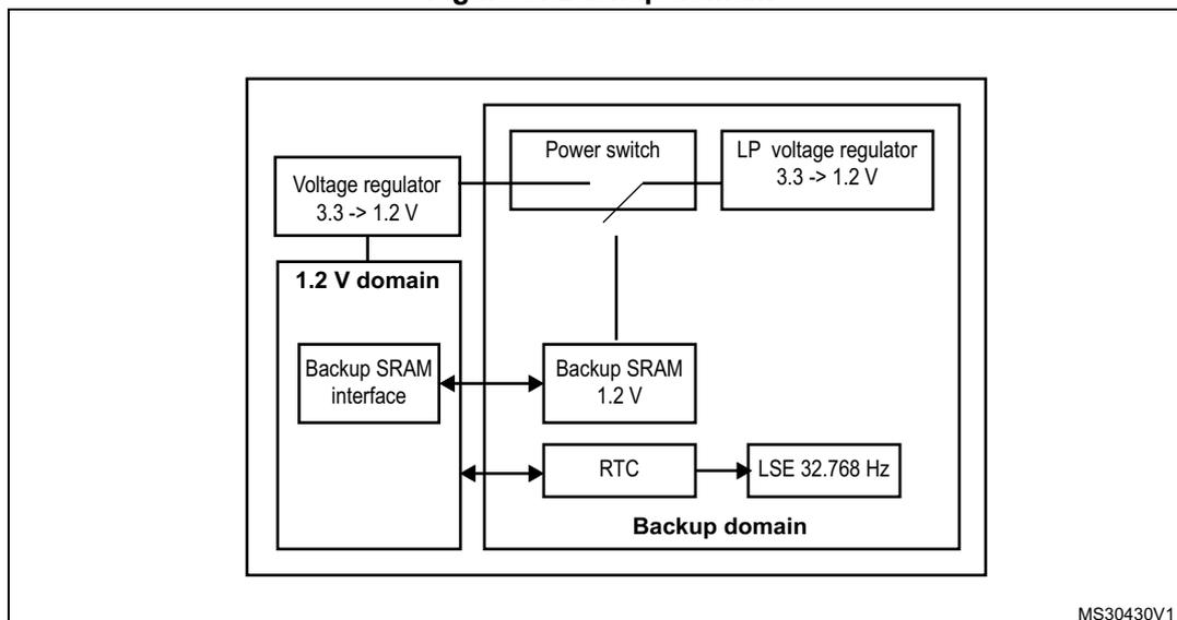
graph TD
    VR[Voltage regulator 3.3 -> 1.2 V] --> Domain12[1.2 V domain]
    subgraph Domain12 [1.2 V domain]
        BSI[Backup SRAM interface] <--> BS[Backup SRAM 1.2 V]
        BSI <--> RTC[RTC]
    end
    PS[Power switch] --> BS
    LPVR[LP voltage regulator 3.3 -> 1.2 V] --> BS
    RTC <--> LSE[LSE 32.768 Hz]
    subgraph BD [Backup domain]
        PS
        LPVR
        Domain12
        LSE
    end
4.1.6 Voltage regulator
An embedded linear voltage regulator supplies all the digital circuitries except for the backup domain and the Standby circuitry. The regulator output voltage is around 1.2 V.
This voltage regulator requires two external capacitors to be connected to two dedicated pins, \( V_{CAP\_1} \) and \( V_{CAP\_2} \) available in all packages. Specific pins must be connected either to \( V_{SS} \) or \( V_{DD} \) to activate or deactivate the voltage regulator. These pins depend on the package.
When activated by software, the voltage regulator is always enabled after Reset. It works in three different modes depending on the application modes (Run, Stop, or Standby mode).
- • In Run mode , the main regulator supplies full power to the 1.2 V domain (core, memories and digital peripherals). In this mode, the regulator output voltage (around 1.2 V) can be scaled by software to different voltage values (scale 1, scale 2, and scale 3 can be configured through \( VOS[1:0] \) bits of the PWR_CR1 register). The scale can be modified only when the PLL is OFF and the HSI or HSE clock source is selected as system clock source. The new value programmed is active only when the PLL is ON. When the PLL is OFF, the voltage scale 3 is automatically selected.
The voltage scaling allows optimizing the power consumption when the device is clocked below the maximum system frequency. After exit from Stop mode, the voltage
scale 3 is automatically selected. (see Section 4.4.1: PWR power control register (PWR_CR1) ).
2 operating modes are available:
- – Normal mode: The CPU and core logic operate at maximum frequency at a given voltage scaling (scale 1, scale 2 or scale 3)
- – Over-drive mode: This mode allows the CPU and the core logic to operate at a higher frequency than the normal mode for the voltage scaling scale 1 and scale 2.
- • In Stop mode: the main regulator or low-power regulator supplies a low-power voltage to the 1.2V domain, thus preserving the content of registers and internal SRAM.
The voltage regulator can be put either in main regulator mode (MR) or in low-power mode (LPR). Both modes can be configured by software as follows:
- – Normal mode: the 1.2 V domain is preserved in nominal leakage mode. It is the default mode when the main regulator (MR) or the low-power regulator (LPR) is enabled.
- – Under-drive mode: the 1.2 V domain is preserved in reduced leakage mode. This mode is only available with the main regulator or the low-power regulator mode (see Table 14 ).
- • In Standby mode: the regulator is powered down. The content of the registers and SRAM are lost except for the Standby circuitry and the backup domain.
Note: Over-drive and under-drive mode are not available when the regulator is bypassed.
For more details, refer to the voltage regulator section in the datasheets.
Table 14. Voltage regulator configuration mode versus device operating mode (1)
| Voltage regulator configuration | Run mode | Sleep mode | Stop mode | Standby mode |
|---|---|---|---|---|
| Normal mode | MR | MR | MR or LPR | - |
| Over-drive mode (2) | MR | MR | - | - |
| Under-drive mode | - | - | MR or LPR | - |
| Power-down mode | - | - | - | Yes |
1. '-' means that the corresponding configuration is not available.
2. The over-drive mode is not available when \( V_{DD} = 1.8 \) to \( 2.1 \) V.
Entering Over-drive mode
It is recommended to enter Over-drive mode when the application is not running critical tasks and when the system clock source is either HSI or HSE. To optimize the configuration time, enable the Over-drive mode during the PLL lock phase.
To enter Over-drive mode, follow the sequence below:
- 1. Select HSI or HSE as system clock.
- 2. Configure RCC_PLLCFGR register and set PLLON bit of RCC_CR register.
- 3. Set ODEN bit of PWR_CR1 register to enable the Over-drive mode and wait for the ODRDY flag to be set in the PWR_CSR1 register.
- 4. Set the ODSW bit in the PWR_CR1 register to switch the voltage regulator from Normal mode to Over-drive mode. The System will be stalled during the switch but the PLL clock system will be still running during locking phase.
- 5. Wait for the ODSWRDY flag in the PWR_CSR1 to be set.
- 6. Select the required Flash latency as well as AHB and APB prescalers.
- 7. Wait for PLL lock.
- 8. Switch the system clock to the PLL.
- 9. Enable the peripherals that are not generated by the System PLL (I2S clock, LCD-TFT clock, SAI1 clock, USB_48MHz clock....).
Note: The PLLI2S and PLLSAI can be configured at the same time as the system PLL.
During the Over-drive switch activation, no peripheral clocks should be enabled. The peripheral clocks must be enabled once the Over-drive mode is activated.
Entering Stop mode disables the Over-drive mode, as well as the PLL. The application software has to configure again the Over-drive mode and the PLL after exiting from Stop mode.
Exiting from Over-drive mode
It is recommended to exit from Over-drive mode when the application is not running critical tasks and when the system clock source is either HSI or HSE. There are two sequences that allow exiting from over-drive mode:
- • By resetting simultaneously the ODEN and ODSW bits in the PWR_CR1 register (sequence 1)
- • By resetting first the ODSW bit to switch the voltage regulator to Normal mode and then resetting the ODEN bit to disable the Over-drive mode (sequence 2).
Example of sequence 1:
- 1. Select HSI or HSE as system clock source.
- 2. Disable the peripheral clocks that are not generated by the System PLL (I2S clock, LCD-TFT clock, SAI1 clock, USB_48MHz clock,...)
- 3. Reset simultaneously the ODEN and the ODSW bits in the PWR_CR1 register to switch back the voltage regulator to Normal mode and disable the Over-drive mode.
- 4. Wait for the ODWRDY flag of PWR_CSR1 to be reset.
Example of sequence 2:
- 1. Select HSI or HSE as system clock source.
- 2. Disable the peripheral clocks that are not generated by the System PLL (I2S clock, LCD-TFT clock, SAI1 clock, USB_48MHz clock,...).
- 3. Reset the ODSW bit in the PWR_CR1 register to switch back the voltage regulator to Normal mode. The system clock is stalled during voltage switching.
- 4. Wait for the ODW RDY flag of PWR_CSR1 to be reset.
- 5. Reset the ODEN bit in the PWR_CR1 register to disable the Over-drive mode.
Note: During step 3, the ODEN bit remains set and the Over-drive mode is still enabled but not active (ODSW bit is reset). If the ODEN bit is reset instead, the Over-drive mode is disabled and the voltage regulator is switched back to the initial voltage.
4.2 Power supply supervisor
4.2.1 Power-on reset (POR)/power-down reset (PDR)
The device has an integrated POR/PDR circuitry that allows proper operation starting from 1.8 V.
The device remains in Reset mode when \( V_{DD}/V_{DDA} \) is below a specified threshold, \( V_{POR/PDR} \) , without the need for an external reset circuit. For more details concerning the power on/power-down reset threshold, refer to the electrical characteristics of the datasheet.
Figure 9. Power-on reset/power-down reset waveform
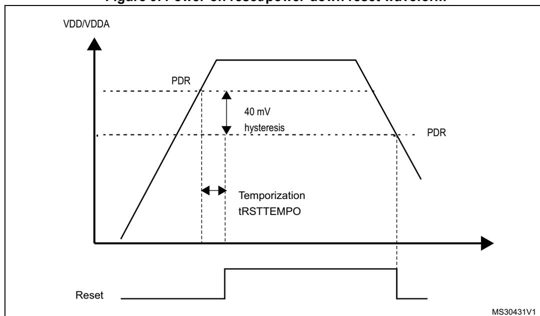
The figure is a timing diagram showing the relationship between the supply voltage \( V_{DD}/V_{DDA} \) and the Reset signal. The top part of the diagram shows the voltage \( V_{DD}/V_{DDA} \) rising from a low value to a high value and then falling. The bottom part shows the Reset signal, which is initially high and goes low when the voltage rises above the Power-Down Reset (PDR) threshold, and goes high again when the voltage falls below the PDR threshold. The PDR threshold is indicated by two dashed horizontal lines with a 40 mV hysteresis between them. The time interval between the voltage crossing the threshold and the Reset signal changing is labeled \( t_{RSTTEMPO} \) (Temporization). The diagram is labeled MS30431V1 in the bottom right corner.
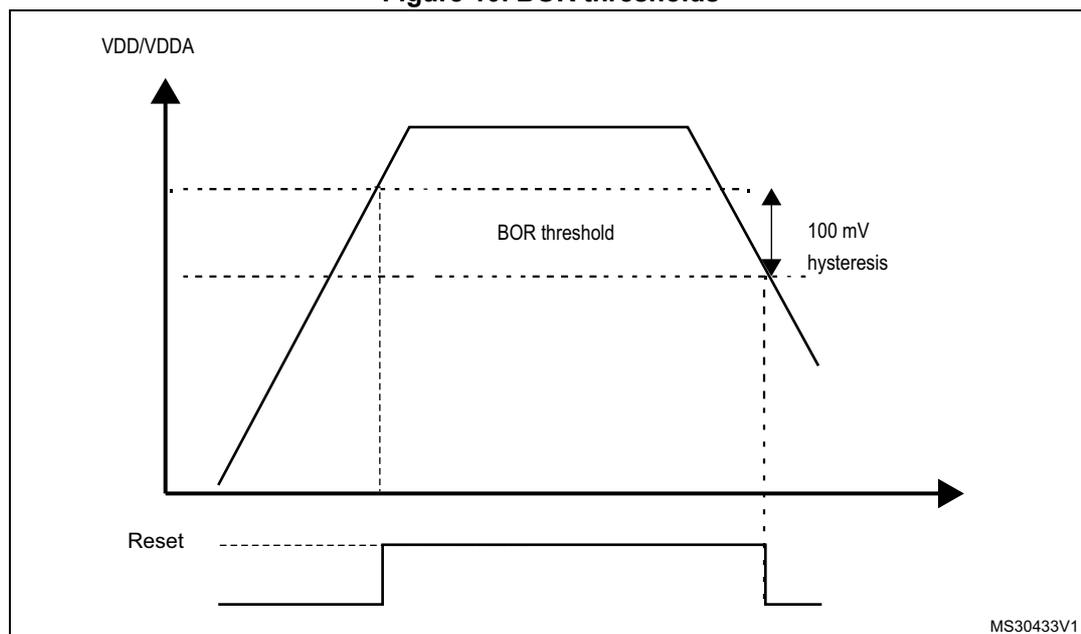
4.2.2 Brownout reset (BOR)
During power on, the Brownout reset (BOR) keeps the device under reset until the supply voltage reaches the specified \( V_{BOR} \) threshold.
\( V_{BOR} \) is configured through device option bytes. By default, BOR is off. 3 programmable \( V_{BOR} \) threshold levels can be selected:
- • BOR Level 3 ( \( V_{BOR3} \) ). Brownout threshold level 3.
- • BOR Level 2 ( \( V_{BOR2} \) ). Brownout threshold level 2.
- • BOR Level 1 ( \( V_{BOR1} \) ). Brownout threshold level 1.
Note: For full details about BOR characteristics, refer to the "Electrical characteristics" section in the device datasheet.
When the supply voltage ( \( V_{DD} \) ) drops below the selected \( V_{BOR} \) threshold, a device reset is generated.
The BOR can be disabled by programming the device option bytes. In this case, the power-on and power-down is then monitored by the POR/ PDR (see Section 4.2.1: Power-on reset (POR)/power-down reset (PDR) ).
The BOR threshold hysteresis is \( \sim 100 \) mV (between the rising and the falling edge of the supply voltage).
Figure 10. BOR thresholds
4.2.3 Programmable voltage detector (PVD)
You can use the PVD to monitor the \( V_{DD} \) power supply by comparing it to a threshold selected by the PLS[2:0] bits in the PWR power control register (PWR_CR1) .
The PVD is enabled by setting the PVDE bit.
A PVDO flag is available, in the PWR power control/status register (PWR_CSR1) , to indicate if \( V_{DD} \) is higher or lower than the PVD threshold. This event is internally connected
to the EXTI line16 and can generate an interrupt if enabled through the EXTI registers. The PVD output interrupt can be generated when \( V_{DD} \) drops below the PVD threshold and/or when \( V_{DD} \) rises above the PVD threshold depending on EXTI line16 rising/falling edge configuration. As an example the service routine could perform emergency shutdown tasks.
Figure 11. PVD thresholds
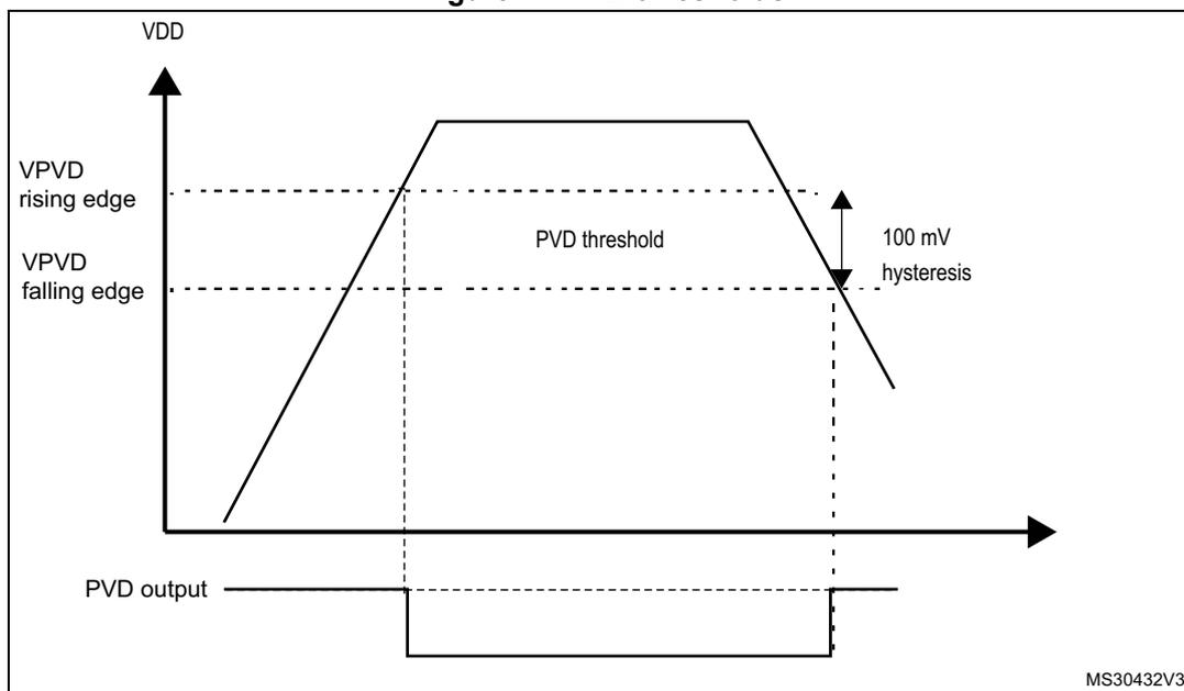
The figure illustrates the Power Supply Voltage Detector (PVD) thresholds. The top graph shows the supply voltage \( V_{DD} \) over time. It features a rising edge and a falling edge. Two horizontal dashed lines represent the \( V_{PVD} \) rising edge and \( V_{PVD} \) falling edge thresholds. The \( V_{PVD} \) threshold is indicated between these two lines. A 100 mV hysteresis is shown between the rising and falling edges. Below the graph, the PVD output is shown as a digital signal that is high when \( V_{DD} \) is below the falling edge threshold and low otherwise. The diagram is labeled MS30432V3.
4.3 Low-power modes
By default, the microcontroller is in Run mode after a system or a power-on reset. In Run mode the CPU is clocked by HCLK and the program code is executed. Several low-power modes are available to save power when the CPU does not need to be kept running, for example when waiting for an external event. It is up to the user to select the mode that gives the best compromise between low-power consumption, short startup time and available wakeup sources.
The devices feature three low-power modes:
- • Sleep mode (Cortex ® -M7 core stopped, peripherals kept running)
- • Stop mode (all clocks are stopped)
- • Standby mode (1.2 V domain powered off)
In addition, the power consumption in Run mode can be reduced by one of the following means:
- • Slowing down the system clocks
- • Gating the clocks to the APBx and AHBx peripherals when they are unused.
Entering low-power mode
Low-power modes are entered by the MCU by executing the WFI (Wait For Interrupt), or WFE (Wait for Event) instructions, or when the SLEEPONEXIT bit in the Cortex ® -M7 System Control register is set on Return from ISR.
Entering Low-power mode through WFI or WFE will be executed only if no interrupt is pending or no event is pending.
Exiting low-power mode
The MCU exits from Sleep and Stop modes low-power mode depending on the way the low-power mode was entered:
- • If the WFI instruction or Return from ISR was used to enter the low-power mode, any peripheral interrupt acknowledged by the NVIC can wake up the device.
- • If the WFE instruction is used to enter the low-power mode, the MCU exits the low-power mode as soon as an event occurs. The wakeup event can be generated either by:
- – NVIC IRQ interrupt:
When SEVONPEND = 0 in the Cortex®-M7 System Control register: by enabling an interrupt in the peripheral control register and in the NVIC. When the MCU resumes from WFE, the peripheral interrupt pending bit and the NVIC peripheral IRQ channel pending bit (in the NVIC interrupt clear pending register) have to be cleared. Only NVIC interrupts with sufficient priority will wakeup and interrupt the MCU.
When SEVONPEND = 1 in the Cortex®-M7 System Control register: by enabling an interrupt in the peripheral control register and optionally in the NVIC. When the MCU resumes from WFE, the peripheral interrupt pending bit and when enabled the NVIC peripheral IRQ channel pending bit (in the NVIC interrupt clear pending register) have to be cleared. All NVIC interrupts will wakeup the MCU, even the disabled ones. Only enabled NVIC interrupts with sufficient priority will wakeup and interrupt the MCU.
- – Event
This is done by configuring a EXTI line in event mode. When the CPU resumes from WFE, it is not necessary to clear the EXTI peripheral interrupt pending bit or the NVIC IRQ channel pending bit as the pending bits corresponding to the event line is not set. It may be necessary to clear the interrupt flag in the peripheral.
The MCU exits from Standby low-power mode through an external reset (NRST pin), an IWDG reset, a rising edge on one of the enabled WKUPx pins or a RTC event occurs (see Figure 344: RTC block diagram ).
After waking up from Standby mode, program execution restarts in the same way as after a Reset (boot pin sampling, option bytes loading, reset vector is fetched, etc.).
Only enabled NVIC interrupts with sufficient priority will wakeup and interrupt the MCU.
Table 15. Low-power mode summary
| Mode name | Entry | Wakeup | Effect on 1.2 V domain clocks | Effect on V DD domain clocks | Voltage regulator |
|---|---|---|---|---|---|
| Sleep (Sleep now or Sleep-on-exit) | WFI | Any interrupt | CPU CLK OFF no effect on other clocks or analog clock sources | None | ON |
| WFE | Wakeup event |
Table 15. Low-power mode summary (continued)
| Mode name | Entry | Wakeup | Effect on 1.2 V domain clocks | Effect on V DD domain clocks | Voltage regulator |
|---|---|---|---|---|---|
| Stop | SLEEPDEEP bit + WFI or WFE | Any EXTI line (configured in the EXTI registers, internal and external lines) | All 1.2 V domain clocks OFF | HSI and HSE oscillators OFF | Main regulator or Low-Power regulator (depends on PWR power control register (PWR_CR1) ) |
| Standby | PDDS bit + SLEEPDEEP bit + WFI or WFE | WKUP pin rising or falling edge, RTC alarm (Alarm A or Alarm B), RTC Wakeup event, RTC tamper events, RTC time stamp event, external reset in NRST pin, IWDG reset | OFF |
Table 16. Features over all modes (1)
| Peripheral | Run | Sleep | Stop | Standby | V BAT | ||
|---|---|---|---|---|---|---|---|
| Wakeup | Wakeup | ||||||
| CPU | Y | - | - | - | - | - | - |
| Flash access | Y | Y | - | - | - | - | - |
| DTCM RAM | Y | Y | Y | - | - | - | - |
| ITCM RAM | Y | Y | Y | - | - | - | - |
| SRAM1 | Y | Y | Y | - | - | - | - |
| SRAM2 | Y | Y | Y | - | - | - | - |
| FMC | O | O | - | - | - | - | - |
| QUADSPI | O | O | - | - | - | - | - |
| Backup Registers | Y | Y | Y | - | Y | - | Y |
| Backup RAM | Y | Y | Y | - | Y | - | Y |
| Brown-out reset (BOR) | Y | Y | Y | Y | Y | Y | - |
| Programmable voltage detector (PVD) | O | O | O | O | - | - | - |
| High Speed Internal (HSI) | O | O | (2) | - | - | - | - |
| High Speed External (HSE) | O | O | - | - | - | - | - |
| Low Speed Internal (LSI) | O | O | O | - | O | - | - |
| Low Speed External (LSE) | O | O | O | - | O | - | O |
| RTC | O | O | O | O | O | O | O |
| Peripheral | Run | Sleep | Stop | Standby | VBAT | ||
|---|---|---|---|---|---|---|---|
| Wakeup | Wakeup | ||||||
| Number of RTC tamper pins | 3 | 3 | 3 | 3 | 3 | 3 | 2 |
| CRC calculation unit | O | O | - | - | - | - | - |
| GPIOs | Y | Y | Y | Y | 6 pins | 2 tamper | |
| DMA | O | O | - | - | - | - | - |
| Chrom-Art Accelerator (DMA2D) | O | O | - | - | - | - | - |
| LCD-TFT | O | O | - | - | - | - | - |
| DCMI | O | O | - | - | - | - | - |
| USARTx (x=1..8) | O | O | - | - | - | - | - |
| I2Cx (x=1,2,3,4) | O | O | - | - | - | - | - |
| SPIx (x=1..6) | O | O | - | - | - | - | - |
| SAIx (x=1,2) | O | O | - | - | - | - | - |
| SPDIFRX | O | O | - | - | - | - | - |
| ADCx (x=1,2,3) | O | O | - | - | - | - | - |
| DACx (x=1,2) | O | O | - | - | - | - | - |
| Temperature sensor | O | O | - | - | - | - | - |
| Timers (TIMx) | O | O | - | - | - | - | - |
| Low-power timer 1 (LPTIM1) | O | O | O | O | - | - | - |
| Independent watchdog (IWDG) | O | O | O | O | O | O | - |
| Window watchdog (WWDG) | O | O | - | - | - | - | - |
| Systick timer | O | O | - | - | - | - | - |
| Random number generator (RNG) | O | O | - | - | - | - | - |
| Cryptographic processor (CRYP) | O | O | - | - | - | - | - |
| Hash processor (HASH) | O | O | - | - | - | - | - |
| SDMMC1, SDMMC2 | O | O | - | - | - | - | - |
| CANx (x=1,3) | O | O | - | - | - | - | - |
| USB OTG FS | O | O | - | O | - | - | - |
| USB OTG HS | O | O | - | O | - | - | - |
| Ethernet | O | O | - | O | - | - | - |
| HDMI-CEC | O | O | - | - | - | - | - |
| DSI-Host | O | O | - | - | - | - | - |
| Peripheral | Run | Sleep | Stop | Standby | VBAT | ||
|---|---|---|---|---|---|---|---|
| Wakeup | Wakeup | ||||||
| JPEG codec | O | O | - | - | - | - | - |
| MDIO slave | O | O | O | O | - | - | - |
| DFSDM1 | O | O | - | - | - | - | - |
- Legend: Y = Yes (Enable). O = Optional (Disable by default. Can be enabled by software). - = Not available. Wakeup highlighted in gray.
- Some peripherals with wakeup from Stop capability can request HSI to be enabled. In this case, HSI is woken up by the peripheral, and only feeds the peripheral which requested it. HSI is automatically put off when the peripheral does not need it anymore.
4.3.1 Debug mode
By default, the debug connection is lost when the device enters in Stop or Standby mode while the debug features are used. This is due to the fact that the Cortex®-M7 core is no longer clocked.
However, by setting some configuration bits in the DBGMCU_CR register, the software can be debugged even when using the low-power modes extensively. For more details, refer to Section 40.16.1: Debug support for low-power modes .
4.3.2 Run mode
Slowing down system clocks
In Run mode the speed of the system clocks (SYSCLK, HCLK, PCLK1, PCLK2) can be reduced by programming the prescaler registers. These prescalers can also be used to slow down peripherals before entering Sleep mode.
For more details refer to Section 41.3.3: RCC clock configuration register (RCC_CFGR) .
Peripheral clock gating
In Run mode, the HCLKx and PCLKx for individual peripherals and memories can be stopped at any time to reduce power consumption.
To further reduce power consumption in Sleep mode the peripheral clocks can be disabled prior to executing the WFI or WFE instructions.
Peripheral clock gating is controlled by the AHB1 peripheral clock enable register (RCC_AHB1ENR), AHB2 peripheral clock enable register (RCC_AHB2ENR), AHB3 peripheral clock enable register (RCC_AHB3ENR) (see Section 41.3.10: RCC AHB1 peripheral clock register (RCC_AHB1ENR) , Section 41.3.11: RCC AHB2 peripheral clock enable register (RCC_AHB2ENR) , and Section 41.3.12: RCC AHB3 peripheral clock enable register (RCC_AHB3ENR) ).
Disabling the peripherals clocks in Sleep mode can be performed automatically by resetting the corresponding bit in RCC_AHBxLPENR and RCC_APBxLPENR registers.
4.3.3 Low-power mode
Entering low-power mode
Low-power modes are entered by the MCU executing the WFI (Wait For Interrupt), or WFE (Wait For Event) instructions, or when the SLEEPONEXIT bit in the Cortex®-M7 System Control register is set on Return from ISR.
Exiting low-power mode
From Sleep and Stop modes the MCU exits low-power mode depending on the way the mode was entered:
- • If the WFI instruction or Return from ISR was used to enter the low-power mode, any peripheral interrupt acknowledged by the NVIC can wake up the device
- • If the WFE instruction was used to enter the low-power mode, the MCU exits the mode as soon as an event occurs. The wakeup event can be generated either by:
- – NVIC IRQ interrupt
- - When SEVEONPEND=0 in the Cortex®-M7 System Control register.
- – NVIC IRQ interrupt
By enabling an interrupt in the peripheral control register and in the NVIC. When the MCU resumes from WFE, the peripheral interrupt pending bit and the NVIC peripheral IRQ channel pending bit (in the NVIC interrupt clear pending register) have to be cleared.
Only NVIC interrupts with sufficient priority will wakeup and interrupt the MCU.
- - When SEVEONPEND=1 in the Cortex®-M7 System Control register.
By enabling an interrupt in the peripheral control register and optionally in the NVIC. When the MCU resumes from WFE, the peripheral interrupt pending bit and (when enabled) the NVIC peripheral IRQ channel pending bit (in the NVIC interrupt clear pending register) have to be cleared.
All NVIC interrupts will wakeup the MCU, even the disabled ones.
Only enabled NVIC interrupts with sufficient priority will wakeup and interrupt the MCU.
- - Event
Configuring a EXTI line in event mode. When the CPU resumes from WFE, it is not necessary to clear the EXTI peripheral interrupt pending bit or the NVIC IRQ channel pending bit as the pending bits corresponding to the event line is not set. It may be necessary to clear the interrupt flag in the peripheral.
From Standby mode the MCU exits Low-power mode through an external reset (NRST pin), an IWDG reset, a rising edge on one of the enabled WKUPx pins or a RTC event (see Figure 344: RTC block diagram ).
4.3.4 Sleep mode
I/O states in Sleep mode
In Sleep mode, all I/O pins keep the same state as in Run mode.
Entering Sleep mode
The Sleep mode is entered by executing the WFI (Wait For Interrupt) or WFE (Wait for Event) instructions. Two options are available to select the Sleep mode entry mechanism, depending on the SLEEPONEXIT bit in the Cortex ® -M7 System Control register:
- • Sleep-now: if the SLEEPONEXIT bit is cleared, the MCU enters Sleep mode as soon as WFI or WFE instruction is executed.
- • Sleep-on-exit: if the SLEEPONEXIT bit is set, the MCU enters Sleep mode as soon as it exits the lowest priority ISR.
Refer to Table 17 and Table 18 for details on how to enter Sleep mode.
Exiting Sleep mode
If the WFI instruction is used to enter Sleep mode, any peripheral interrupt acknowledged by the nested vectored interrupt controller (NVIC) can wake up the device from Sleep mode.
If the WFE instruction is used to enter Sleep mode, the MCU exits Sleep mode as soon as an event occurs. The wakeup event can be generated either by:
- • Enabling an interrupt in the peripheral control register but not in the NVIC, and enabling the SEVONPEND bit in the Cortex ® -M7 System Control register. When the MCU resumes from WFE, the peripheral interrupt pending bit and the peripheral NVIC IRQ channel pending bit (in the NVIC interrupt clear pending register) have to be cleared.
- • Or configuring an external or internal EXTI line in event mode. When the CPU resumes from WFE, it is not necessary to clear the peripheral interrupt pending bit or the NVIC IRQ channel pending bit as the pending bit corresponding to the event line is not set.
This mode offers the lowest wakeup time as no time is wasted in interrupt entry/exit.
Refer to Table 17 and Table 18 for more details on how to exit Sleep mode.
Table 17. Sleep-now entry and exit
| Sleep-now mode | Description |
|---|---|
| Mode entry | WFI (Wait for Interrupt) or WFE (Wait for Event) while:
Refer to the Cortex ® -M7 System Control register. On Return from ISR while:
Refer to the Cortex ® -M7 System Control register. |
| Mode exit | If WFI or Return from ISR was used for entry: Interrupt: Refer to Table 44: STM32F75xxx and STM32F74xxx vector table If WFE was used for entry and SEVONPEND = 0 Wakeup event: Refer to Section 11.3: Wakeup event management If WFE was used for entry and SEVONPEND = 1 Interrupt even when disabled in NVIC: refer to Table 44: STM32F75xxx and STM32F74xxx vector table and Wakeup event (see Section 11.3: Wakeup event management ). |
| Wakeup latency | None |
Table 18. Sleep-on-exit entry and exit
| Sleep-on-exit | Description |
|---|---|
| Mode entry | WFI (Wait for Interrupt) or WFE (Wait for Event) while:
On Return from ISR while:
|
| Mode exit | Interrupt: refer to Table 44: STM32F75xxx and STM32F74xxx vector table |
| Wakeup latency | None |
4.3.5 Stop mode
The Stop mode is based on the Cortex®-M7 deepsleep mode combined with peripheral clock gating. The voltage regulator can be configured either in normal or low-power mode. In Stop mode, all clocks in the 1.2 V domain are stopped, the PLLs, the HSI and the HSE RC oscillators are disabled. Internal SRAM and register contents are preserved.
In Stop mode, the power consumption can be further reduced by using additional settings in the PWR_CR1 register. However this will induce an additional startup delay when waking up from Stop mode (see Table 19 ).
Table 19. Stop operating modes
| Voltage Regulator Mode | UDEN[1:0] bits | MRUDS bit | LPUDS bit | LPDS bit | FPDS bit | Wakeup latency | |
|---|---|---|---|---|---|---|---|
| Normal mode | STOP MR (Main Regulator) | - | 0 | - | 0 | 0 | HSI RC startup time |
| STOP MR- FPD | - | 0 | - | 0 | 1 | HSI RC startup time + Flash wakeup time from power-down mode | |
| STOP LP | - | 0 | 0 | 1 | 0 | HSI RC startup time + regulator wakeup time from LP mode | |
| STOP LP-FPD | - | - | 0 | 1 | 1 | HSI RC startup time + Flash wakeup time from power-down mode + regulator wakeup time from LP mode | |
Table 19. Stop operating modes (continued)
| Voltage Regulator Mode | UDEN[1:0] bits | MRUDS bit | LPUDS bit | LPDS bit | FPDS bit | Wakeup latency | |
|---|---|---|---|---|---|---|---|
| Under-drive Mode | STOP UMR-FPD | 3 | 1 | - | 0 | - | HSI RC startup time + Flash wakeup time from power-down mode + Main regulator wakeup time from under-drive mode + Core logic to nominal mode |
| STOP ULP-FPD | 3 | - | 1 | 1 | - | HSI RC startup time + Flash wakeup time from power-down mode + regulator wakeup time from LP under-drive mode + Core logic to nominal mode | |
I/O states in Stop mode
In stop mode, all I/Os pins keep the same state as in the run mode
Entering Stop mode
The Stop mode is entered according to Entering low-power mode , when the SLEEPDEEP bit in Cortex ® -M7 System Control register is set.
Refer to Table 20 for details on how to enter the Stop mode.
When the microcontroller enters in Stop mode, the voltage scale 3 is automatically selected. To further reduce power consumption in Stop mode, the internal voltage regulator can be put in low-power or low voltage mode. This is configured by the LPDS, MRUDS, LPUDS and UDEN bits of the PWR power control register (PWR_CR1) .
If Flash memory programming is ongoing, the Stop mode entry is delayed until the memory access is finished.
If an access to the APB domain is ongoing, The Stop mode entry is delayed until the APB access is finished.
If the Over-drive mode was enabled before entering Stop mode, it is automatically disabled during when the Stop mode is activated.
In Stop mode, the following features can be selected by programming individual control bits:
- • Independent watchdog (IWDG): the IWDG is started by writing to its Key register or by hardware option. Once started it cannot be stopped except by a Reset. See Section 30.3 in Section 30: Independent watchdog (IWDG) .
- • Real-time clock (RTC): this is configured by the RTCEN bit in the RCC backup domain control register (RCC_BDCR)
- • Internal RC oscillator (LSI RC): this is configured by the LSION bit in the RCC clock control & status register (RCC_CSR) .
- • External 32.768 kHz oscillator (LSE OSC): this is configured by the LSEON bit in the RCC backup domain control register (RCC_BDCR) .
The ADC or DAC can also consume power during the Stop mode, unless they are disabled before entering it. To disable them, the ADON bit in the ADC_CR2 register and the ENx bit in the DAC_CR register must both be written to 0.
Note: Before entering Stop mode, it is recommended to enable the clock security system (CSS) feature to prevent external oscillator (HSE) failure from impacting the internal MCU behavior.
Exiting Stop mode
Refer to Table 20 for more details on how to exit Stop mode.
When exiting Stop mode by issuing an interrupt or a wakeup event, the HSI RC oscillator is selected as system clock.
If the Under-drive mode was enabled, it is automatically disabled after exiting Stop mode.
When the voltage regulator operates in low-power mode, an additional startup delay is incurred when waking up from Stop mode. By keeping the internal regulator ON during Stop mode, the consumption is higher although the startup time is reduced.
When the voltage regulator operates in Under-drive mode, an additional startup delay is induced when waking up from Stop mode.
Table 20. Stop mode entry and exit (STM32F76xxx and STM32F77xxx)
| Stop mode | Description |
|---|---|
| Mode entry | WFI (Wait for Interrupt) or WFE (Wait for Event) while:
On Return from ISR while:
Note: To enter Stop mode, all EXTI Line pending bits (in Pending register (EXTI_PR) ), all peripheral interrupts pending bits, the RTC Alarm (Alarm A and Alarm B), RTC wakeup, RTC tamper, and RTC time stamp flags, must be reset. Otherwise, the Stop mode entry procedure is ignored and program execution continues. |
| Stop mode | Description |
|---|---|
| Mode exit | If WFI or Return from ISR was used for entry: If WFE was used for entry and SEVONPEND = 0: If WFE was used for entry and SEVONPEND = 1:
|
| Wakeup latency | Refer to Table 19: Stop operating modes |
4.3.6 Standby mode
The Standby mode allows to achieve the lowest power consumption. It is based on the Cortex ® -M7 deepsleep mode, with the voltage regulator disabled. The 1.2 V domain is consequently powered off. The PLLs, the HSI oscillator and the HSE oscillator are also switched off. SRAM and register contents are lost except for registers in the backup domain (RTC registers, RTC backup register and backup SRAM), and Standby circuitry (see Figure 5 ).
Entering Standby mode
The Standby mode is entered according to Entering low-power mode, when the SLEEPDEEP bit in the Cortex ® -M7 System Control register is set.
Refer to Table 21 for more details on how to enter Standby mode.
In Standby mode, the following features can be selected by programming individual control bits:
- • Independent watchdog (IWDG): the IWDG is started by writing to its Key register or by hardware option. Once started it cannot be stopped except by a reset. See Section 30.3 in Section 30: Independent watchdog (IWDG) .
- • Real-time clock (RTC): this is configured by the RTCEN bit in the backup domain control register (RCC_BDCR)
- • Internal RC oscillator (LSI RC): this is configured by the LSION bit in the Control/status register (RCC_CSR).
- • External 32.768 kHz oscillator (LSE OSC): this is configured by the LSEON bit in the backup domain control register (RCC_BDCR)
Exiting Standby mode
The microcontroller exits Standby mode when an external Reset (NRST pin), an IWDG Reset, a rising or falling edge on WKUP pin, an RTC alarm, a tamper event, or a time stamp
event is detected. All registers are reset after wakeup from Standby except for PWR power control/status register (PWR_CSR1) .
After waking up from Standby mode, program execution restarts in the same way as after a Reset (boot pin sampling, vector reset is fetched, etc.). The SBF status flag in the PWR power control/status register (PWR_CSR1) indicates that the MCU was in Standby mode.
Refer to Table 21 for more details on how to exit Standby mode.
Table 21. Standby mode entry and exit
| Standby mode | Description |
|---|---|
| Mode entry | WFI (Wait for Interrupt) or WFE (Wait for Event) while:
On return from ISR while:
|
| Mode exit | WKUP pin rising or falling edge, RTC alarm (Alarm A and Alarm B), RTC wakeup, tamper event, time stamp event, external reset in NRST pin, IWDG reset. |
| Wakeup latency | Reset phase. |
I/O states in Standby mode
In Standby mode, all I/O pins are high impedance except for:
- • Reset pad (still available)
- • PC13 if configured for tamper, time stamp, RTC Alarm out, or RTC clock calibration out
- • WKUP pins (PA0/PA2/PC1/PC13/PI8/PI11), if enabled
4.3.7 Programming the RTC alternate functions to wake up the device from the Stop and Standby modes
The MCU can be woken up from a low-power mode by an RTC alternate function.
The RTC alternate functions are the RTC alarms (Alarm A and Alarm B), RTC wakeup, RTC tamper event detection and RTC time stamp event detection.
These RTC alternate functions can wake up the system from the Stop and Standby low-power modes.
The system can also wake up from low-power modes without depending on an external interrupt (Auto-wakeup mode), by using the RTC alarm or the RTC wakeup events.
The RTC provides a programmable time base for waking up from the Stop or Standby mode at regular intervals.
For this purpose, two of the three alternate RTC clock sources can be selected by programming the RTCSEL[1:0] bits in the RCC backup domain control register (RCC_BDCR) :
- • Low-power 32.768 kHz external crystal oscillator (LSE OSC)
This clock source provides a precise time base with a very low-power consumption (additional consumption of less than 1 µA under typical conditions) - • Low-power internal RC oscillator (LSI RC)
This clock source has the advantage of saving the cost of the 32.768 kHz crystal. This internal RC oscillator is designed to use minimum power.
RTC alternate functions to wake up the device from the Stop mode
- • To wake up the device from the Stop mode with an RTC alarm event, it is necessary to:
- a) Configure the EXTI Line 17 to be sensitive to rising edges (Interrupt or Event modes)
- b) Enable the RTC Alarm Interrupt in the RTC_CR register
- c) Configure the RTC to generate the RTC alarm
- • To wake up the device from the Stop mode with an RTC tamper or time stamp event, it is necessary to:
- a) Configure the EXTI Line 21 to be sensitive to rising edges (Interrupt or Event modes)
- b) Enable the RTC time stamp Interrupt in the RTC_CR register or the RTC tamper interrupt in the RTC_TAFCR register
- c) Configure the RTC to detect the tamper or time stamp event
- • To wake up the device from the Stop mode with an RTC wakeup event, it is necessary to:
- a) Configure the EXTI Line 22 to be sensitive to rising edges (Interrupt or Event modes)
- b) Enable the RTC wakeup interrupt in the RTC_CR register
- c) Configure the RTC to generate the RTC Wakeup event
RTC alternate functions to wake up the device from the Standby mode
- • To wake up the device from the Standby mode with an RTC alarm event, it is necessary to:
- a) Enable the RTC alarm interrupt in the RTC_CR register
- b) Configure the RTC to generate the RTC alarm
- • To wake up the device from the Standby mode with an RTC tamper or time stamp event, it is necessary to:
- a) Enable the RTC time stamp interrupt in the RTC_CR register or the RTC tamper interrupt in the RTC_TAFCR register
- b) Configure the RTC to detect the tamper or time stamp event
- • To wake up the device from the Standby mode with an RTC wakeup event, it is necessary to:
- a) Enable the RTC wakeup interrupt in the RTC_CR register
- b) Configure the RTC to generate the RTC wakeup event
Safe RTC alternate function wakeup flag clearing sequence
To avoid bouncing on the pins onto which the RTC alternate functions are mapped, and exit correctly from the Stop and Standby modes, it is recommended to follow the sequence below before entering the Standby mode:
- • When using RTC alarm to wake up the device from the low-power modes:
- a) Disable the RTC alarm interrupt (ALRAIE or ALRBIE bits in the RTC_CR register)
- b) Clear the RTC alarm (ALRAF/ALRBF) flag
- c) Enable the RTC alarm interrupt
- d) Re-enter the low-power mode
- • When using RTC wakeup to wake up the device from the low-power modes:
- a) Disable the RTC Wakeup interrupt (WUTIE bit in the RTC_CR register)
- b) Enable the RTC Wakeup interrupt
- c) Re-enter the low-power mode
- • When using RTC tamper to wake up the device from the low-power modes:
- a) Disable the RTC tamper interrupt (TAMPIE bit in the RTC_TAFCR register)
- b) Clear the Tamper (TAMP1F/TSF) flag
- c) Enable the RTC tamper interrupt
- d) Re-enter the low-power mode
- • When using RTC time stamp to wake up the device from the low-power modes:
- a) Disable the RTC time stamp interrupt (TSIE bit in RTC_CR)
- b) Clear the RTC time stamp (TSF) flag
- c) Enable the RTC TimeStamp interrupt
- d) Re-enter the low-power mode
4.4 Power control registers
4.4.1 PWR power control register (PWR_CR1)
Address offset: 0x00
Reset value: 0x0000 C000 (reset by wakeup from Standby mode)
| 31 | 30 | 29 | 28 | 27 | 26 | 25 | 24 | 23 | 22 | 21 | 20 | 19 | 18 | 17 | 16 |
|---|---|---|---|---|---|---|---|---|---|---|---|---|---|---|---|
| Res. | Res. | Res. | Res. | Res. | Res. | Res. | Res. | Res. | Res. | Res. | Res. | UDEN[1:0] | ODSWEN | ODEN | |
| rw | rw | rw | rw | ||||||||||||
| 15 | 14 | 13 | 12 | 11 | 10 | 9 | 8 | 7 | 6 | 5 | 4 | 3 | 2 | 1 | 0 |
|---|---|---|---|---|---|---|---|---|---|---|---|---|---|---|---|
| VOS[1:0] | ADCDC1 | Res. | MRUDS | LPUDS | FPDS | DBP | PLS[2:0] | PVDE | CSBF | Res. | PDDS | LPDS | |||
| rw | rw | rw | rw | rw | rw | rw | rw | rw | rw | rw | rc_w1 | rw | rw | ||
Bits 31:20 Reserved, must be kept at reset value.
Bits 19:18 UDEN[1:0] : Under-drive enable in stop mode
These bits are set by software. They allow to achieve a lower power consumption in Stop mode but with a longer wakeup time.
When set, the digital area has less leakage consumption when the device enters Stop mode.
00: Under-drive disable
01: Reserved
10: Reserved
11: Under-drive enable
Bit 17 ODSWEN : Over-drive switching enabled.
This bit is set by software. It is cleared automatically by hardware after exiting from Stop mode or when the ODEN bit is reset. When set, It is used to switch to Over-drive mode.
To set or reset the ODSWEN bit, the HSI or HSE must be selected as system clock.
The ODSWEN bit must only be set when the ODRDY flag is set to switch to Over-drive mode.
0: Over-drive switching disabled
1: Over-drive switching enabled
Note: On any over-drive switch (enabled or disabled), the system clock will be stalled during the internal voltage set up.
Bit 16 ODEN : Over-drive enable
This bit is set by software. It is cleared automatically by hardware after exiting from Stop mode. It is used to enabled the Over-drive mode in order to reach a higher frequency.
To set or reset the ODEN bit, the HSI or HSE must be selected as system clock. When the ODEN bit is set, the application must first wait for the Over-drive ready flag (ODRDY) to be set before setting the ODSWEN bit.
0: Over-drive disabled
1: Over-drive enabled
Bits 15:14 VOS[1:0] : Regulator voltage scaling output selection
These bits control the main internal voltage regulator output voltage to achieve a trade-off between performance and power consumption when the device does not operate at the maximum frequency (refer to the STM32F76xxx and STM32F77xxx datasheets for more details).
These bits can be modified only when the PLL is OFF. The new value programmed is active only when the PLL is ON. When the PLL is OFF, the voltage scale 3 is automatically selected.
00: Reserved (Scale 3 mode selected)
01: Scale 3 mode
10: Scale 2 mode
11: Scale 1 mode (reset value)
Bit 13 ADCD1 :
0: No effect.
1: Refer to AN4073 for details on how to use this bit.
Note: This bit can only be set when operating at supply voltage range 2.7 to 3.6V.
Bit 12 Reserved, must be kept at reset value.
Bit 11 MRUDS : Main regulator in deepsleep under-drive mode
This bit is set and cleared by software.
0: Main regulator ON when the device is in Stop mode
1: Main Regulator in under-drive mode and Flash memory in power-down when the device is in Stop under-drive mode.
Bit 10 LPUDS : Low-power regulator in deepsleep under-drive mode
This bit is set and cleared by software.
0: Low-power regulator ON if LPDS bit is set when the device is in Stop mode
1: Low-power regulator in under-drive mode if LPDS bit is set and Flash memory in power-down when the device is in Stop under-drive mode.
Bit 9 FPDS : Flash power-down in Stop mode
When set, the Flash memory enters power-down mode when the device enters Stop mode. This allows to achieve a lower consumption in stop mode but a longer restart time.
0: Flash memory not in power-down when the device is in Stop mode
1: Flash memory in power-down when the device is in Stop mode
Bit 8 DBP : Disable backup domain write protection
In reset state, the RCC_BDCR register, the RTC registers (including the backup registers), and the BRE bit of the PWR_CSR1 register, are protected against parasitic write access. This bit must be set to enable write access to these registers.
0: Access to RTC and RTC Backup registers and backup SRAM disabled
1: Access to RTC and RTC Backup registers and backup SRAM enabled
Bits 7:5 PLS[2:0] : Programmable voltage detector level selectionThese bits are written by software to select the voltage threshold detected by the programmable voltage detector
- 000: 2.0 V
- 001: 2.1 V
- 010: 2.3 V
- 011: 2.5 V
- 100: 2.6 V
- 101: 2.7 V
- 110: 2.8 V
- 111: 2.9 V
Note: Refer to the electrical characteristics of the datasheet for more details.
Note: These bits cannot be reset by a peripheral reset through the PWRRST bit in the RCC_APB1RSTR register. It is reset only by a system reset.
These bits are write protected when PVD_LOCK is set in the system configuration.
Bit 4 PVDE : Programmable voltage detector enableThis bit is set and cleared by software.
- 0: PVD disabled
- 1: PVD enabled
Note: This bit cannot be reset by a peripheral reset through the PWRRST bit in the RCC_APB1RSTR register. It is reset only by a system reset.
This bit is write protected when PVD_LOCK is set in the system configuration.
Bit 3 CSBF : Clear standby flagThis bit is always read as 0.
- 0: No effect
- 1: Clear the SDF Standby Flag (write)
Bit 2 Reserved, must be kept at reset value
Bit 1 PDDS : Power-down deepsleepThis bit is set and cleared by software. It works together with the LPDS bit.
- 0: Enter Stop mode when the CPU enters deepsleep. The regulator status depends on the LPDS bit.
- 1: Enter Standby mode when the CPU enters deepsleep.
This bit is set and cleared by software. It works together with the PDDS bit.
- 0: Main voltage regulator ON during Stop mode
- 1: Low-power voltage regulator ON during Stop mode
4.4.2 PWR power control/status register (PWR_CSR1)
Address offset: 0x04
Reset value: 0x0000 0000 (not reset by wakeup from Standby mode)
Additional APB cycles are needed to read this register versus a standard APB read.
| 31 | 30 | 29 | 28 | 27 | 26 | 25 | 24 | 23 | 22 | 21 | 20 | 19 18 | 17 | 16 | |
|---|---|---|---|---|---|---|---|---|---|---|---|---|---|---|---|
| Res. | Res. | Res. | Res. | Res. | Res. | Res. | Res. | Res. | Res. | Res. | Res. | UDRDY[1:0] | ODSWRDY | ODRDY | |
| rc_w1 | rc_w1 | r | r | ||||||||||||
| 15 | 14 | 13 | 12 | 11 | 10 | 9 | 8 | 7 | 6 | 5 | 4 | 3 | 2 | 1 | 0 |
|---|---|---|---|---|---|---|---|---|---|---|---|---|---|---|---|
| Res. | VOSRDY | Res. | Res. | Res. | Res. | BRE | Res. | Res. | Res. | Res. | Res. | BRR | PVDO | SBF | WUIF |
| r | rw | r | r | r | r |
Bits 31:20 Reserved, must be kept at reset value.
Bits 19:18 UDRDY[1:0] : Under-drive ready flag
These bits are set by hardware when MCU enters stop Under-drive mode and exits. When the Under-drive mode is enabled, these bits are not set as long as the MCU has not entered stop mode yet. They are cleared by programming them to 1.
00: Under-drive is disabled
01: Reserved
10: Reserved
11: Under-drive mode is activated in Stop mode.
Bit 17 ODSWRDY : Over-drive mode switching ready
0: Over-drive mode is not active.
1: Over-drive mode is active on digital area on 1.2 V domain
Bit 16 ODRDY : Over-drive mode ready
0: Over-drive mode not ready.
1: Over-drive mode ready
Bit 14 VOSRDY : Regulator voltage scaling output selection ready bit
0: Not ready
1: Ready
Bits 13:10 Reserved, must be kept at reset value.
Bit 9 BRE : Backup regulator enable
When set, the Backup regulator (used to maintain backup SRAM content in Standby and
\(
V_{BAT}
\)
modes) is enabled. If BRE is reset, the backup regulator is switched off. The backup SRAM can still be used but its content will be lost in the Standby and
\(
V_{BAT}
\)
modes. Once set, the application must wait that the Backup Regulator Ready flag (BRR) is set to indicate that the data written into the RAM will be maintained in the Standby and
\(
V_{BAT}
\)
modes.
0: Backup regulator disabled
1: Backup regulator enabled
Note: This bit is not reset when the device wakes up from Standby mode or by a system reset or power reset. It is reset by a backup domain reset.
The DBP bit of PWR_CR register must be set to 1 before PWR_CSR.BRE can be written.
Bits 8:4 Reserved, must be kept at reset value.
Bit 3 BRR : Backup regulator ready
Set by hardware to indicate that the Backup Regulator is ready.
0: Backup Regulator not ready
1: Backup Regulator ready
Note: This bit is not reset when the device wakes up from Standby mode or by a system reset or power reset. It is reset by a backup domain reset.
Bit 2 PVDO : Programmable voltage detector output
This bit is set and cleared by hardware. It is valid only if PVD is enabled by the PVDE bit.
0: \( V_{DD} \) is higher than the PVD threshold selected with the PLS[2:0] bits.
1: \( V_{DD} \) is lower than the PVD threshold selected with the PLS[2:0] bits.
Note: The PVD is stopped by Standby mode. For this reason, this bit is equal to 0 after Standby or reset until the PVDE bit is set.
Bit 1 SBF : Standby flag
This bit is set by hardware and cleared only by a POR/PDR (power-on reset/power-down reset) or by setting the CSBF bit in the PWR power control register (PWR_CR1)
0: Device has not been in Standby mode
1: Device has been in Standby mode
Bit 0 WUIF : Wakeup internal flag
This bit is set when a wakeup is detected on the internal wakeup line in standby mode. It is cleared when all internal wakeup sources are cleared.
0: No wakeup internal event occurred
1: A wakeup event was detected from the RTC alarm (Alarm A or Alarm B), RTC Tamper event, RTC TimeStamp event or RTC Wakeup
4.4.3 PWR power control/status register 2 (PWR_CR2)
Address offset: 0x08
Reset value: 0x0000 0000 (not reset by wakeup from Standby mode)
| 31 | 30 | 29 | 28 | 27 | 26 | 25 | 24 | 23 | 22 | 21 | 20 | 19 | 18 | 17 | 16 |
|---|---|---|---|---|---|---|---|---|---|---|---|---|---|---|---|
| Res. | Res. | Res. | Res. | Res. | Res. | Res. | Res. | Res. | Res. | Res. | Res. | Res. | Res. | Res. | Res. |
| 15 | 14 | 13 | 12 | 11 | 10 | 9 | 8 | 7 | 6 | 5 | 4 | 3 | 2 | 1 | 0 |
| Res. | Res. | WUPP6 | WUPP5 | WUPP4 | WUPP3 | WUPP2 | WUPP1 | Res. | Res. | CWUPF6 | CWUPF5 | CWUPF4 | CWUPF3 | CWUPF2 | CWUPF1 |
| rw | rw | rw | rw | rw | rw | r | r | r | r | r | r |
Bits 31:14 Reserved, always read as 0.
Bit 13 WUPP6 : Wakeup pin polarity bit for PI11
These bits define the polarity used for event detection on external wake-up pin PI11.
0: Detection on rising edge
1: Detection on falling edge
Bit 12 WUPP5 : Wakeup pin polarity bit for PI8
These bits define the polarity used for event detection on external wake-up pin PI8.
0: Detection on rising edge
1: Detection on falling edge
- Bit 11
WUPP4
: Wakeup pin polarity bit for PC13
These bits define the polarity used for event detection on external wake-up pin PC13.
0: Detection on rising edge
1: Detection on falling edge - Bit 10
WUPP3
: Wakeup pin polarity bit for PC1
These bits define the polarity used for event detection on external wake-up pin PC1.
0: Detection on rising edge
1: Detection on falling edge - Bit 9
WUPP2
: Wakeup pin polarity bit for PA2
These bits define the polarity used for event detection on external wake-up pin PA2.
0: Detection on rising edge
1: Detection on falling edge - Bit 8
WUPP1
: Wakeup pin polarity bit for PA0
These bits define the polarity used for event detection on external wake-up pin PA0.
0: Detection on rising edge
1: Detection on falling edge - Bits 7:6 Reserved, always read as 0
- Bit 5
CWUPF6
: Clear Wakeup Pin flag for PI11
These bits are always read as 0
0: No effect
1: Clear the WUPF Wakeup Pin flag after 2 System clock cycles. - Bit 4
CWUPF5
: Clear Wakeup Pin flag for PI8
These bits are always read as 0
0: No effect
1: Clear the WUPF Wakeup Pin flag after 2 System clock cycles. - Bit 3
CWUPF4
: Clear Wakeup Pin flag for PC13
These bits are always read as 0
0: No effect
1: Clear the WUPF Wakeup Pin flag after 2 System clock cycles. - Bit 2
CWUPF3
: Clear Wakeup Pin flag for PC1
These bits are always read as 0
0: No effect
1: Clear the WUPF Wakeup Pin flag after 2 System clock cycles. - Bit 1
CWUPF2
: Clear Wakeup Pin flag for PA2
These bits are always read as 0
0: No effect
1: Clear the WUPF Wakeup Pin flag after 2 System clock cycles. - Bit 0
CWUPF1
: Clear Wakeup Pin flag for PA0
These bits are always read as 0
0: No effect
1: Clear the WUPF Wakeup Pin flag after 2 System clock cycles.
4.4.4 PWR power control register 2 (PWR_CSR2)
Address offset: 0x0C
Reset value: 0x0000 0000 (reset by wakeup from Standby mode, except wakeup flags which are reset by RESET pin)
Additional APB cycles are needed to read this register versus a standard APB read.
| 31 | 30 | 29 | 28 | 27 | 26 | 25 | 24 | 23 | 22 | 21 | 20 | 19 | 18 | 17 | 16 |
|---|---|---|---|---|---|---|---|---|---|---|---|---|---|---|---|
| Res. | Res. | Res. | Res. | Res. | Res. | Res. | Res. | Res. | Res. | Res. | Res. | Res. | Res. | Res. | Res. |
| 15 | 14 | 13 | 12 | 11 | 10 | 9 | 8 | 7 | 6 | 5 | 4 | 3 | 2 | 1 | 0 |
| Res. | Res. | EWUP6 | EWUP5 | EWUP4 | EWUP3 | EWUP2 | EWUP1 | Res. | Res. | WUPF6 | WUPF5 | WUPF4 | WUPF3 | WUPF2 | WUPF1 |
| rw | rw | rw | rw | rw | rw | r | r | r | r | r | r |
Bits 31:14 Reserved, always read as 0.
Bit 13 EWUP6 : Enable Wakeup pin for PI11
This bit is set and cleared by software.
0: An event on WKUP pin PI11 does not wake-up the device from Standby mode.
1: A rising or falling edge on WKUP pin PI11 wakes-up the system from Standby mode.
Bit 12 EWUP5 : Enable Wakeup pin for PI8
This bit is set and cleared by software.
0: An event on WKUP pin PI8 does not wake-up the device from Standby mode.
1: A rising or falling edge on WKUP pin PI8 wakes-up the system from Standby mode.
Bit 11 EWUP4 : Enable Wakeup pin for PC13
This bit is set and cleared by software.
0: An event on WKUP pin PC13 does not wake-up the device from Standby mode.
1: A rising or falling edge on WKUP pin PC13 wakes-up the system from Standby mode.
Bit 10 EWUP3 : Enable Wakeup pin for PC1
This bit is set and cleared by software.
0: An event on WKUP pin PC1 does not wake-up the device from Standby mode.
1: A rising or falling edge on WKUP pin PC1 wakes-up the system from Standby mode.
Bit 9 EWUP2 : Enable Wakeup pin for PA2
This bit is set and cleared by software.
0: An event on WKUP pin PA2 does not wake-up the device from Standby mode.
1: A rising or falling edge on WKUP pin PA2 wakes-up the system from Standby mode.
Bit 8 EWUP1 : Enable Wakeup pin for PA0
This bit is set and cleared by software.
0: An event on WKUP pin PA0 does not wake-up the device from Standby mode.
1: A rising or falling edge on WKUP pin PA0 wakes-up the system from Standby mode.
Bits 7:6 Reserved, always read as 0
Bit 5 WUPF6 : Wakeup Pin flag for PI11This bit is set by hardware and cleared only by a Reset pin or by setting the CWUPF6 bit in the PWR power control register 2 (PWR_CR2).
0: No Wakeup event occurred
1: A wakeup event is detected on WKUP PI11
Note: An additional wakeup event is detected if WKUP pin is enabled (by setting the EWUP6 bit) when WKUP pin PI11 level is already high.
Bit 4 WUPF5 : Wakeup Pin flag for PI8This bit is set by hardware and cleared only by a Reset pin or by setting the CWUPF5 bit in the PWR power control register 2 (PWR_CR2).
0: No Wakeup event occurred
1: A wakeup event is detected on WKUP PI8
Note: An additional wakeup event is detected if WKUP pin is enabled (by setting the EWUP5 bit) when WKUP pin PI8 level is already high.
Bit 3 WUPF4 : Wakeup Pin flag for PC13This bit is set by hardware and cleared only by a Reset pin or by setting the CWUPF4 bit in the PWR power control register 2 (PWR_CR2).
0: No Wakeup event occurred
1: A wakeup event is detected on WKUP PC13
Note: An additional wakeup event is detected if WKUP pin is enabled (by setting the EWUP4 bit) when WKUP pin PC13 level is already high.
Bit 2 WUPF3 : Wakeup Pin flag for PC1This bit is set by hardware and cleared only by a Reset pin or by setting the CWUPF3 bit in the PWR power control register 2 (PWR_CR2).
0: No Wakeup event occurred
1: A wakeup event is detected on WKUP PC1
Note: An additional wakeup event is detected if WKUP pin is enabled (by setting the EWUP3 bit) when WKUP pin PC1 level is already high.
Bit 1 WUPF2 : Wakeup Pin flag for PA2This bit is set by hardware and cleared only by a Reset pin or by setting the CWUPF2 bit in the PWR power control register 2 (PWR_CR2).
0: No Wakeup event occurred
1: A wakeup event is detected on WKUP PA2
Note: An additional wakeup event is detected if WKUP pin is enabled (by setting the EWUP2 bit) when WKUP pin PA2 level is already high.
Bit 0 WUPF1 : Wakeup Pin flag for PA0This bit is set by hardware and cleared only by a Reset pin or by setting the CWUPF1 bit in the PWR power control register 2 (PWR_CR2).
0: No Wakeup event occurred
1: A wakeup event is detected on WKUP PA0
Note: An additional wakeup event is detected if WKUP pin is enabled (by setting the EWUP1 bit) when WKUP pin PA0 level is already high.
4.5 PWR register map
The following table summarizes the PWR registers.
Table 22. PWR - register map and reset values
| Offset | Register | 31 | 30 | 29 | 28 | 27 | 26 | 25 | 24 | 23 | 22 | 21 | 20 | 19 | 18 | 17 | 16 | 15 | 14 | 13 | 12 | 11 | 10 | 9 | 8 | 7 | 6 | 5 | 4 | 3 | 2 | 1 | 0 | |
|---|---|---|---|---|---|---|---|---|---|---|---|---|---|---|---|---|---|---|---|---|---|---|---|---|---|---|---|---|---|---|---|---|---|---|
| 0x000 | PWR_CR1 | Res. | Res. | Res. | Res. | Res. | Res. | Res. | Res. | Res. | Res. | Res. | Res. | UDEN[1:0] | ODSWEN | ODEN | VOS[1:0] | ADDCD1 | Res. | MRUDS | LPUDS | FPDS | DBP | PLS[2:0] | PVDE | CSBF | Res. | PDDS | LPDS | |||||
| Reset value | 1 | 1 | 1 | 1 | 1 | 1 | 0 | 1 | 1 | 0 | 0 | 0 | 0 | 0 | 0 | 0 | 0 | 0 | ||||||||||||||||
| 0x004 | PWR_CSR1 | Res. | Res. | Res. | Res. | Res. | Res. | Res. | Res. | Res. | Res. | Res. | Res. | UDRDY[1:0] | ODSWRDY | ODRDY | Res. | VOSRDY | Res. | Res. | Res. | Res. | BRE | Res. | Res. | Res. | Res. | Res. | Res. | Res. | BRR | PVDO | SBF | WUIF |
| Reset value | 0 | 0 | 0 | 0 | 0 | 0 | 0 | 0 | 0 | |||||||||||||||||||||||||
| 0x008 | PWR_CR2 | Res. | Res. | Res. | Res. | Res. | Res. | Res. | Res. | Res. | Res. | Res. | Res. | Res. | Res. | Res. | Res. | Res. | Res. | EWUP6 | EWUP5 | EWUP4 | EWUP3 | EWUP2 | EWUP1 | Res. | Res. | Res. | Res. | Res. | Res. | Res. | Res. | |
| Reset value | 0 | 0 | 0 | 0 | 0 | 0 | ||||||||||||||||||||||||||||
| 0x00C | PWR_CSR2 | Res. | Res. | Res. | Res. | Res. | Res. | Res. | Res. | Res. | Res. | Res. | Res. | Res. | Res. | Res. | Res. | Res. | Res. | EWUP6 | EWUP5 | EWUP4 | EWUP3 | EWUP2 | EWUP1 | Res. | Res. | Res. | Res. | Res. | Res. | Res. | Res. | |
| Reset value | 0 | 0 | 0 | 0 | 0 | 0 | ||||||||||||||||||||||||||||
Refer to Section 2.2 on page 76 for the register boundary addresses.