2. System and memory overview
2.1 System architecture
The main system architecture is based on 2 sub-systems:
- • An AXI to multi AHB bridge converting AXI4 protocol to AHB-Lite protocol:
- – 1x AXI to 64-bit AHB bridge connected to the embedded flash
- – 3x AXI to 32bit AHB bridge connected to AHB bus matrix
- • A multi-AHB Bus-Matrix
Figure 1. System architecture for STM32F76xxx and STM32F77xxx devices
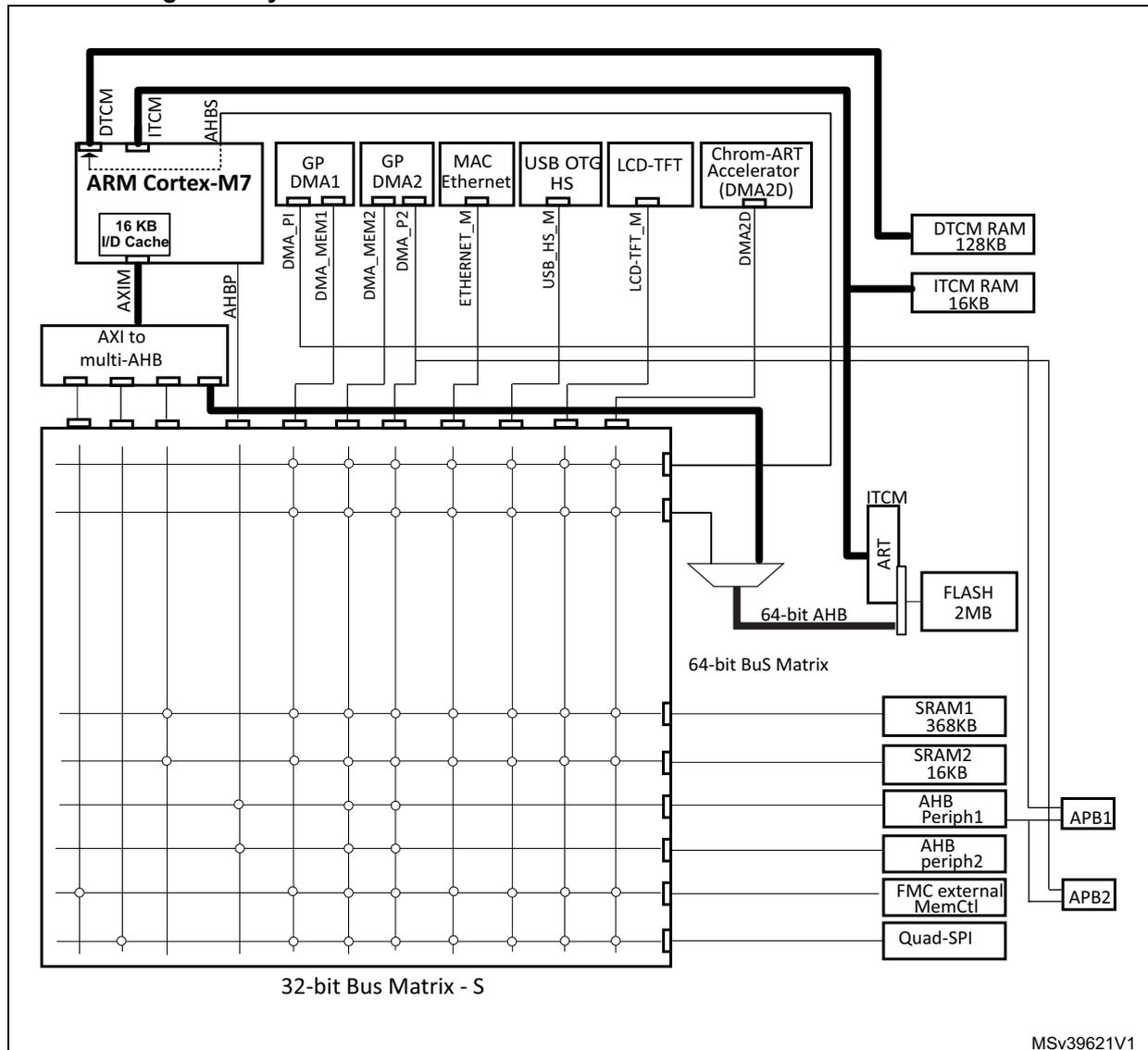
The diagram illustrates the system architecture for STM32F76xxx and STM32F77xxx devices. At the top, the ARM Cortex-M7 core is shown with its 16 KB I/D Cache . It is connected to DTCM and ITCM memory. Below the core, an AXI to multi-AHB bridge is connected via AXIM . This bridge connects to a 32-bit Bus Matrix - S . The bus matrix is connected to various peripherals and memory blocks via AHB and AXI interfaces. The peripherals include GP DMA1 , GP DMA2 , MAC Ethernet , USB OTG HS , LCD-TFT , and Chrom-ART Accelerator (DMA2D) . The memory hierarchy includes DTCM RAM 128KB , ITCM RAM 16KB , FLASH 2MB , SRAM1 368KB , and SRAM2 16KB . The 64-bit AHB bridge is connected to the FLASH 2MB . The 64-bit Bus Matrix is connected to the SRAM1 368KB and SRAM2 16KB . The APB1 and APB2 buses are connected to the 32-bit Bus Matrix - S via AHB Periph1 and AHB periph2 respectively. Other components include FMC external MemCtl and Quad-SPI . The diagram is labeled with MSv39621V1 in the bottom right corner.
The multi-AHB Bus-Matrix interconnects all the masters and slaves and it consists on:
- – 32-bit multi-AHB Bus-Matrix
- – 64-bit multi-AHB Bus-Matrix: It interconnects the 64-bit AHB bus from CPU through the AXI to AHB bridge and the 32-bit AHB bus from GP DMAs and peripheral DMAs up-sized to 64-bit to the internal flash.
The multi AHB bus matrix interconnects:
- • 12 bus masters:
- – 3x32-bit AHB bus Cortex ® -M7 AXI Master bus 64-bits, splitted 4 masters through the AXI to AHB bridge.
- – 1x64-bit AHB bus connected to the embedded flash
- – Cortex ® -M7 AHB Peripherals bus
- – DMA1 memory bus
- – DMA2 memory bus
- – DMA2 peripheral bus
- – Ethernet DMA bus
- – USB OTG HS DMA bus
- – LCD Controller DMA-bus
- – Chrom-Art Accelerator ™ (DMA2D) memory bus
- • Eight bus slaves:
- – the embedded Flash on AHB bus (for Flash read/write access, for code execution and data access)
- – Cortex ® -M7 AHBS slave interface for DMAs data transfer on DTCM RAM only.
- – Main internal SRAM1 (368 KB)
- – Auxiliary internal SRAM2 (16 KB)
- – AHB1peripherals including AHB to APB bridges and APB peripherals
- – AHB2 peripherals
- – FMC
- – Quad-SPI
2.1.1 Multi AHB BusMatrix
The multi AHB BusMatrix manages the access arbitration between masters. The arbitration uses a round-robin algorithm.
It provides access from a master to a slave, enabling concurrent access and efficient operation even when several high-speed peripherals work simultaneously.
The DTCM and ITCM RAMs (tightly coupled memories) are not part of the bus matrix.
The Data TCM RAM is accessible by the GP-DMAs and peripherals DMAs through specific AHB slave bus of the CPU.
The instruction TCM RAM is reserved only for CPU. it is accessed at CPU clock speed with 0 wait states. The architecture is shown in Figure 1 .
2.1.2 AHB/APB bridges (APB)
The two AHB/APB bridges, APB1 and APB2, provide full synchronous connections between the AHB and the two APB buses, allowing flexible selection of the peripheral frequency.
Refer to the device datasheets for more details on APB1 and APB2 maximum frequencies, and to Table 1 for the address mapping of AHB and APB peripherals.
After each device reset, all peripheral clocks are disabled (except for the SRAM, DTCM, ITCM RAM and Flash memory interface). Before using a peripheral you have to enable its clock in the RCC_AHBxENR or RCC_APBxENR register.
Note: When a 16- or an 8-bit access is performed on an APB register, the access is transformed into a 32-bit access: the bridge duplicates the 16- or 8-bit data to feed the 32-bit vector.
2.1.3 CPU AXIM bus
This bus connects the Cortex ® -M7 with FPU core to the multi-AHB Bus-Matrix through AXI to AHB bridge. There are 4 AXI bus targets:
- – CPU AXI bus access 1: The target of this AXI bus is the external memory FMC containing code or data. For the NAND Bank mapped at address 0x8000 0000 to 0x8FFF FFFF, the MPU memory attribute for this space must be reconfigured by software to Device.
- – CPU AXI bus access 2: The target of this AXI bus is the external memory Quad-SPI containing code or data.
- – CPU AXI bus access 3: The target of this AXI bus is the internal SRAMs (SRAM1 and SRAM2) containing code or data.
- – CPU AXI bus access 4: The target of this AXI bus is the embedded Flash mapped on AXI interface containing code or data.
2.1.4 ITCM bus
This bus is used by the Cortex ® -M7 and AHBS for instruction fetches and data access on the embedded flash mapped on ITCM interface and instruction fetches and data access on ITCM RAM.
2.1.5 DTCM bus
This bus is used by the Cortex ® -M7 for data access on the DTCM RAM. It can be also used for instruction fetches.
2.1.6 CPU AHBS bus
This bus connects the AHB Slave bus of the Cortex ® -M7 to the BusMatrix. This bus is used by DMAs and Peripherals DMAs for Data transfer on DTCM RAM only.
The ITCM bus is not accessible on AHBS. So the DMA data transfer to/from ITCM RAM is not supported. For DMA transfer to/from Flash on ITCM interface, all the transfers are forced through AHB bus
2.1.7 AHB peripheral bus
This bus connects the AHB Peripheral bus of the Cortex ® -M7 to the BusMatrix. This bus is used by the core to perform all data accesses to peripherals.
The target of this bus is the AHB1 peripherals including the APB peripherals and the AHB2 peripherals.
2.1.8 DMA memory bus
This bus connects the DMA memory bus master interface to the BusMatrix. It is used by the DMA to perform transfer to/from memories. The targets of this bus are data memories: internal SRAM1, SRAM2 and DTCM (through the AHBS bus of Cortex ® -M7) internal Flash memory and external memories through the FMC or Quad-SPI.
2.1.9 DMA peripheral bus
This bus connects the DMA peripheral master bus interface to the AHB-to-APB bridges or the BusMatrix. This bus is used by the DMA to access peripherals or to perform memory-to-memory transfers. The targets of this bus are the APB peripherals plus AHB peripherals and data memories (internal SRAM1, SRAM2 and DTCM internal Flash memory and external memories through the FMC or Quad-SPI) for DMA2.
2.1.10 Ethernet DMA bus
This bus connects the Ethernet DMA master interface to the BusMatrix. This bus is used by the Ethernet DMA to load/store data to a memory. The targets of this bus are data memories: internal SRAM1, SRAM2 and DTCM (through the AHBS bus of Cortex ® -M7) internal Flash memory, and external memories through the FMC or Quad-SPI.
2.1.11 USB OTG HS DMA bus
This bus connects the USB OTG HS DMA master interface to the BusMatrix. This bus is used by the USB OTG DMA to load/store data to a memory. The targets of this bus are data memories: internal SRAM1, SRAM2 and DTCM (through the AHBS bus of Cortex ® -M7), internal Flash memory, and external memories through the FMC or Quad-SPI.
2.1.12 LCD-TFT controller DMA bus
This bus connects the LCD controller DMA master interface to the BusMatrix. It is used by the LCD-TFT DMA to load data from a memory. The targets of this bus are data memories: internal SRAM1, SRAM2 and DTCM (through the AHBS bus of Cortex ® -M7), external memories through FMC or Quad-SPI, and internal Flash memory.
2.1.13 DMA2D bus
This bus connects the DMA2D master interface to the BusMatrix. This bus is used by the DMA2D graphic Accelerator to load/store data to a memory. The targets of this bus are data memories: internal SRAM1, SRAM2 and DTCM (through the AHBS bus of Cortex ® -M7), external memories through FMC or Quad-SPI, and internal Flash memory.
2.2 Memory organization
2.2.1 Introduction
Program memory, data memory, registers and I/O ports are organized within the same linear 4-Gbyte address space.
The bytes are coded in memory in Little Endian format. The lowest numbered byte in a word is considered the word's least significant byte and the highest numbered byte the most significant.
The addressable memory space is divided into eight main blocks, of 512 Mbytes each.
2.2.2 Memory map and register boundary addresses
Figure 2. Memory map
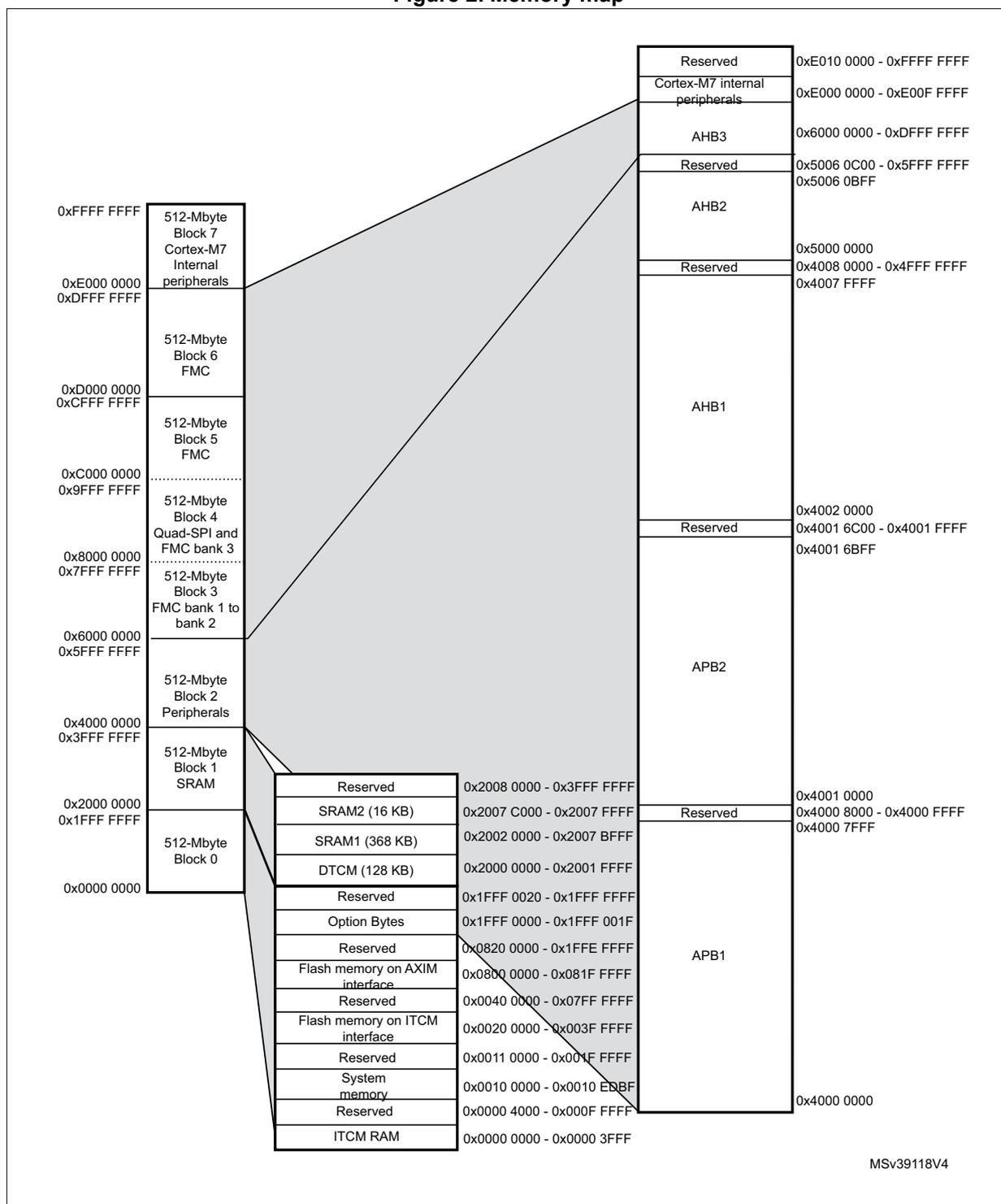
The memory map illustrates the organization of memory for the RM0410 microcontroller. It is divided into several 512-Mbyte blocks, each with specific internal components and address ranges.
| Memory Block | Internal Component | Address Range |
|---|---|---|
| 512-Mbyte Block 7 Cortex-M7 Internal peripherals | Reserved | 0xE010 0000 - 0xFFFF FFFF |
| Cortex-M7 internal peripherals | 0xE000 0000 - 0xE00F FFFF | |
| 512-Mbyte Block 6 FMC | AHB3 | 0x6000 0000 - 0xDFFF FFFF |
| Reserved | 0x5006 0C00 - 0x5FFF FFFF 0x5006 0BFF | |
| AHB2 | 0x5000 0000 | |
| Reserved | 0x4008 0000 - 0x4FFF FFFF 0x4007 FFFF | |
| 512-Mbyte Block 5 FMC | AHB1 | 0x4002 0000 |
| Reserved | 0x4001 6C00 - 0x4001 FFFF 0x4001 6BFF | |
| APB2 | ||
| Reserved | 0x4001 0000 | |
| 512-Mbyte Block 4 Quad-SPI and FMC bank 3 | Reserved | 0x4000 8000 - 0x4000 FFFF 0x4000 7FFF |
| APB1 | 0x4000 0000 | |
| 512-Mbyte Block 3 FMC bank 1 to bank 2 | Reserved | 0x2008 0000 - 0x3FFF FFFF |
| SRAM2 (16 KB) | 0x2007 C000 - 0x2007 FFFF | |
| 512-Mbyte Block 2 Peripherals | SRAM1 (368 KB) | 0x2002 0000 - 0x2007 BFFF |
| DTCM (128 KB) | 0x2000 0000 - 0x2001 FFFF | |
| 512-Mbyte Block 1 SRAM | Reserved | 0x1FFF 0020 - 0x1FFF FFFF |
| Option Bytes | 0x1FFF 0000 - 0x1FFF 001F | |
| Reserved | 0x0820 0000 - 0x1FFE FFFF | |
| Flash memory on AXIM interface | 0x0800 0000 - 0x081F FFFF | |
| Reserved | 0x0040 0000 - 0x07FF FFFF | |
| Flash memory on ITCM interface | 0x0020 0000 - 0x003F FFFF | |
| Reserved | 0x0011 0000 - 0x001F FFFF | |
| System memory | 0x0010 0000 - 0x0010 EBBF | |
| Reserved | 0x0000 4000 - 0x000F FFFF | |
| ITCM RAM | 0x0000 0000 - 0x0000 3FFF | |
| Reserved | ||
| Option Bytes |
MSv39118V4
All the memory map areas that are not allocated to on-chip memories and peripherals are considered "Reserved". For the detailed mapping of available memory and register areas, refer to the following table.
The following table gives the boundary addresses of the peripherals available in the devices.
Table 1. STM32F76xxx and STM32F77xxx register boundary addresses
| Boundary address | Peripheral | Bus | Register map |
|---|---|---|---|
| 0xA000 1000 - 0xA0001FFF | QUADSPI Control Register | AHB3 | QUADSPI register map |
| 0xA000 0000 - 0xA000 0FFF | FMC control register | FMC register map | |
| 0x5006 0800 - 0x5006 0BFF | RNG | AHB2 | RNG register map |
| 0x5006 0400 - 0x5006 07FF | HASH | HASH register map | |
| 0x5006 0000 - 0x5006 03FF | CRYP | CRYP register map | |
| 0x5005 1000 - 0x5005 1FFF | JPEG | JPEG codec register map | |
| 0x5005 0000 - 0x5005 03FF | DCMI | DCMI register map | |
| 0x5000 0000 - 0x5003 FFFF | USB OTG FS | OTG_FS/OTG_HS register map | |
| 0x4004 0000 - 0x4007 FFFF | USB OTG HS | OTG_FS/OTG_HS register map | |
| 0x4002 B000 - 0x4002 BBFF | Chrom-ART (DMA2D) | AHB1 | DMA2D register map |
| 0x4002 8000 - 0x4002 93FF | ETHERNET MAC | Ethernet register maps | |
| 0x4002 6400 - 0x4002 67FF | DMA2 | DMA register map | |
| 0x4002 6000 - 0x4002 63FF | DMA1 | ||
| 0x4002 4000 - 0x4002 4FFF | BKPSRAM | RCC register map | |
| 0x4002 3C00 - 0x4002 3FFF | Flash interface register | Flash interface register map | |
| 0x4002 3800 - 0x4002 3BFF | RCC | RCC register map | |
| 0x4002 3000 - 0x4002 33FF | CRC | CRC register map | |
| 0x4002 2800 - 0x4002 2BFF | GPIOK | GPIO register map | |
| 0x4002 2400 - 0x4002 27FF | GPIOJ | ||
| 0x4002 2000 - 0x4002 23FF | GPIOI | GPIO register map | |
| 0x4002 1C00 - 0x4002 1FFF | GPIOH | ||
| 0x4002 1800 - 0x4002 1BFF | GPIOG | ||
| 0x4002 1400 - 0x4002 17FF | GPIOF | ||
| 0x4002 1000 - 0x4002 13FF | GPIOE | ||
| 0x4002 0C00 - 0x4002 0FFF | GPIO D | ||
| 0x4002 0800 - 0x4002 0BFF | GPIOC | ||
| 0x4002 0400 - 0x4002 07FF | GPIOB | ||
| 0x4002 0000 - 0x4002 03FF | GPIOA |
Table 1. STM32F76xxx and STM32F77xxx register boundary addresses (continued)
| Boundary address | Peripheral | Bus | Register map |
|---|---|---|---|
| 0x4001 7800 - 0x4001 7BFF | MDIOS | APB2 | MDIOS register map |
| 0x4001 7400 - 0x4001 77FF | DFSDM1 | DFSDM register map | |
| 0x4001 6C00 - 0x4001 73FF | DSI Host | DSI register map | |
| 0x4001 6800 - 0x4001 6BFF | LCD-TFT | LTDC register map | |
| 0x4001 5C00 - 0x4001 5FFF | SAI2 | SAI register map | |
| 0x4001 5800 - 0x4001 5BFF | SAI1 | SAI register map | |
| 0x4001 5400 - 0x4001 57FF | SPI6 | SPI/I2S register map | |
| 0x4001 5000 - 0x4001 53FF | SPI5 | ||
| 0x4001 4800 - 0x4001 4BFF | TIM11 | TIM10/TIM11/TIM13/TIM14 register map | |
| 0x4001 4400 - 0x4001 47FF | TIM10 | ||
| 0x4001 4000 - 0x4001 43FF | TIM9 | TIM9/TIM12 register map | |
| 0x4001 3C00 - 0x4001 3FFF | EXTI | EXTI register map | |
| 0x4001 3800 - 0x4001 3BFF | SYSCFG | SYSCFG register map | |
| 0x4001 3400 - 0x4001 37FF | SPI4 | SPI/I2S register map | |
| 0x4001 3000 - 0x4001 33FF | SPI1 | SPI/I2S register map | |
| 0x4001 2C00 - 0x4001 2FFF | SDMMC1 | SDMMC register map | |
| 0x4001 2000 - 0x4001 23FF | ADC1 - ADC2 - ADC3 | ADC register map | |
| 0x4001 1C00 - 0x4001 1FFF | SDMMC2 | SDMMC register map | |
| 0x4001 1400 - 0x4001 17FF | USART6 | USART register map | |
| 0x4001 1000 - 0x4001 13FF | USART1 | ||
| 0x4001 0400 - 0x4001 07FF | TIM8 | TIM8 register map | |
| 0x4001 0000 - 0x4001 03FF | TIM1 | Section 25.4.28: TIM1 register map on page 948 |
| Boundary address | Peripheral | Bus | Register map |
|---|---|---|---|
| 0x4000 7C00 - 0x4000 7FFF | UART8 | APB1 | USART register map |
| 0x4000 7800 - 0x4000 7BFF | UART7 | ||
| 0x4000 7400 - 0x4000 77FF | DAC | DAC register map | |
| 0x4000 7000 - 0x4000 73FF | PWR | PWR register map | |
| 0x4000 6C00 - 0x4000 6FFF | HDMI-CEC | HDMI-CEC register map | |
| 0x4000 6800 - 0x4000 6BFF | CAN2 | bxCAN register map | |
| 0x4000 6400 - 0x4000 67FF | CAN1 | ||
| 0x4000 6000 - 0x4000 63FF | I2C4 | ||
| 0x4000 5C00 - 0x4000 5FFF | I2C3 | I2C register map | |
| 0x4000 5800 - 0x4000 5BFF | I2C2 | ||
| 0x4000 5400 - 0x4000 57FF | I2C1 | ||
| 0x4000 5000 - 0x4000 53FF | UART5 | ||
| 0x4000 4C00 - 0x4000 4FFF | UART4 | USART register map | |
| 0x4000 4800 - 0x4000 4BFF | USART3 | ||
| 0x4000 4400 - 0x4000 47FF | USART2 | ||
| 0x4000 4000 - 0x4000 43FF | SPDIFRX | SPDIFRX interface register map | |
| 0x4000 3C00 - 0x4000 3FFF | SPI3 / I2S3 | SPI/I2S register map | |
| 0x4000 3800 - 0x4000 3BFF | SPI2 / I2S2 | ||
| 0x4000 3400 - 0x4000 37FF | CAN3 | bxCAN register map | |
| 0x4000 3000 - 0x4000 33FF | IWDG | IWDG register map | |
| 0x4000 2C00 - 0x4000 2FFF | WWDG | WWDG register map | |
| 0x4000 2800 - 0x4000 2BFF | RTC & BKP Registers | RTC register map | |
| 0x4000 2400 - 0x4000 27FF | LPTIM1 | LPTIM register map | |
| 0x4000 2000 - 0x4000 23FF | TIM14 | TIM10/TIM11/TIM13/TIM14 register map | |
| 0x4000 1C00 - 0x4000 1FFF | TIM13 | ||
| 0x4000 1800 - 0x4000 1BFF | TIM12 | TIM9/TIM12 register map | |
| 0x4000 1400 - 0x4000 17FF | TIM7 | TIMx register map | |
| 0x4000 1000 - 0x4000 13FF | TIM6 | ||
| 0x4000 0C00 - 0x4000 0FFF | TIM5 | ||
| 0x4000 0800 - 0x4000 0BFF | TIM4 | TIMx register map | |
| 0x4000 0400 - 0x4000 07FF | TIM3 | ||
| 0x4000 0000 - 0x4000 03FF | TIM2 |
2.3 Embedded SRAM
The STM32F76xxx and STM32F77xxx feature:
- • System SRAM up to 512 Kbytes including Data TCM RAM 128 Kbytes
- • Instruction RAM (ITCM-RAM) 16 Kbytes.
- • 4 Kbytes of backup SRAM (see section 5.1.2: Battery backup domain)
The embedded SRAM is divided into up to four blocks:
- • System SRAM:
- – SRAM1 mapped at address 0x2002 0000 and accessible by all AHB masters from AHB bus Matrix.
- – SRAM2 mapped at address 0x2007 C000 and accessible by all AHB masters from AHB bus Matrix.
- – DTCM-RAM on TCM interface (Tightly Coupled Memory interface) mapped at address 0x2000 0000 and accessible by all AHB masters from AHB bus Matrix but through a specific AHB slave bus of the CPU.
- • Instruction SRAM:
- – Instruction RAM (ITCM-RAM) mapped at address 0x0000 0000 and accessible only by CPU.
The SRAM1 and SRAM2 can be accessed as bytes, half-words (16 bits) or full words (32 bits). While DTCM and ITCM RAMs can be accessed as bytes, half-words (16 bits), full words (32 bits) or double words (64 bits).
2.4 Flash memory overview
The Flash memory interface manages CPU AXI and TCM accesses to the Flash memory. It implements the erase and program Flash memory operations and the read and write protection mechanisms. It accelerates code execution with ART on TCM interface or L1-Cache on AXIM interface.
The Flash memory is organized as follows:
- • A main memory block divided into sectors.
- • A second block:
- – System memory from which the device boots in System memory boot mode
- – 1024 OTP (one-time programmable) bytes for user data.
- – Option bytes to configure read and write protection, BOR level, software/hardware watchdog, boot memory base address and reset when the device is in Standby or Stop mode.
Refer to Section 3: Embedded flash memory (FLASH) for more details.
2.5 Boot configuration
In the STM32F76xxx and STM32F77xxx, two different boot areas can be selected through the BOOT pin and the boot base address programmed in the BOOT_ADD0 and BOOT_ADD1 option bytes as shown in the Table 2 .
Table 2. Boot modes
| Boot mode selection | Boot area | |
|---|---|---|
| BOOT | Boot address option bytes | |
| 0 | BOOT_ADD0[15:0] | Boot address defined by user option byte BOOT_ADD0[15:0] ST programmed value: Flash on ITCM at 0x0020 0000 |
| 1 | BOOT_ADD1[15:0] | Boot address defined by user option byte BOOT_ADD1[15:0] ST programmed value: System bootloader at 0x0010 0000 |
The values on the BOOT pin are latched on the 4th rising edge of SYSCLK after reset release. It is up to the user to set the BOOT pin after reset.
The BOOT pin is also resampled when the device exits the Standby mode. Consequently, they must be kept in the required Boot mode configuration when the device is in the Standby mode.
After startup delay, the selection of the boot area is done before releasing the processor reset.
The BOOT_ADD0 and BOOT_ADD1 address option bytes allows to program any boot memory address from 0x0000 0000 to 0x2007 FFFF which includes:
- • All Flash address space mapped on ITCM or AXIM interface
- • All RAM address space: ITCM, DTCM RAMs and SRAMs mapped on AXIM interface
- • The System memory bootloader
The BOOT_ADD0 / BOOT_ADD1 option bytes can be modified after reset in order to boot from any other boot address after next reset.
If the programmed boot memory address is out of the memory mapped area or a reserved area, the default boot fetch address is programmed as follows:
- – Boot address 0: ITCM-FLASH at 0x0020 0000
- – Boot address 1: ITCM-RAM at 0x0000 0000
When flash level 2 protection is enabled, only boot from Flash (on ITCM or AXIM interface) or system bootloader will be available. If the already programmed boot address in the BOOT_ADD0 and/or BOOT_ADD1 option bytes is out of the memory range or RAM address (on ITCM or AXIM) the default fetch will be forced from Flash on ITCM interface at address 0x00200000.
When the device is in Dual bank mode (nDBANK =0) the application software can either boot from bank 1 or from bank 2. By default Dual boot is deactivated.
To select boot from the Flash memory bank 2, program the nDBOOT bit in the user option bytes. When this bit is reset (nDBOOT =0) and the BOOT pin selects an address in the Flash memory range, the device boots from system memory, and the bootloader jumps to execute the user application programmed in the Flash memory bank 2. For further details, please refer to the application note (AN2606).
Embedded bootloader
The embedded bootloader code is located in the system memory. It is programmed by ST during production. For full information, refer to the application note (AN2606) STM32 microcontroller system memory boot mode.
By default, when the boot from system bootloader is selected, the code is executed from TCM interface. It could be executed from AXIM interface by reprogramming the BOOT_ADDx address option bytes to 0x1FF0 0000.