31. Device electronic signature
The electronic signature is stored in the Flash memory area. It can be read using the JTAG/SWD or the CPU. It contains factory-programmed identification data that allow the user firmware or other external devices to automatically match its interface to the characteristics of the STM32F4xx microcontrollers.
31.1 Unique device ID register (96 bits)
The unique device identifier is ideally suited:
- • for use as serial numbers
- • for use as security keys in order to increase the security of code in flash memory while using and combining this unique ID with software cryptographic primitives and protocols before programming the internal flash memory
- • to activate secure boot processes, etc.
The 96-bit unique device identifier provides a reference number which is unique for any device and in any context. These bits can never be altered by the user.
The 96-bit unique device identifier can also be read in single bytes/half-words/words in different ways and then be concatenated using a custom algorithm.
Base address: 0x1FFF 7A10
Address offset: 0x00
Read only = 0xXXXX XXXX where X is factory-programmed
![Bit layout diagram for the first 32 bits of the unique device ID register. It shows a single row of 32 cells, each containing 'r', representing bits 31:0 (U_ID[31:0]).](/RM0402-STM32F412/69a3cceaf90abfc5f7bd11037cb808e3_img.jpg)
| 31 | 30 | 29 | 28 | 27 | 26 | 25 | 24 | 23 | 22 | 21 | 20 | 19 | 18 | 17 | 16 | 15 | 14 | 13 | 12 | 11 | 10 | 9 | 8 | 7 | 6 | 5 | 4 | 3 | 2 | 1 | 0 | |
| U_ID[31:0] | ||||||||||||||||||||||||||||||||
| r | r | r | r | r | r | r | r | r | r | r | r | r | r | r | r | r | r | r | r | r | r | r | r | r | r | r | r | r | r | r | r | r |
Bits 31:0 U_ID[31:0] : 31:0 unique ID bits
Address offset: 0x04
Read only = 0xXXXX XXXX where X is factory-programmed
![Bit layout diagram for the next 32 bits of the unique device ID register. It shows two rows of 16 cells each. The first row represents bits 31:16 (U_ID[63:48]) and the second row represents bits 15:0 (U_ID[47:32]).](/RM0402-STM32F412/3427870972c224935c2c93cdc329c893_img.jpg)
| 31 | 30 | 29 | 28 | 27 | 26 | 25 | 24 | 23 | 22 | 21 | 20 | 19 | 18 | 17 | 16 |
| U_ID[63:48] | |||||||||||||||
| r | r | r | r | r | r | r | r | r | r | r | r | r | r | r | r |
| 15 | 14 | 13 | 12 | 11 | 10 | 9 | 8 | 7 | 6 | 5 | 4 | 3 | 2 | 1 | 0 |
| U_ID[47:32] | |||||||||||||||
| r | r | r | r | r | r | r | r | r | r | r | r | r | r | r | r |
Bits 31:0 U_ID[63:32] : 63:32 unique ID bits
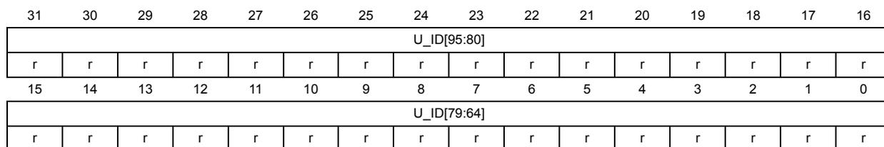
Address offset: 0x08
Read only = 0xXXXX XXXX where X is factory-programmed
| 31 | 30 | 29 | 28 | 27 | 26 | 25 | 24 | 23 | 22 | 21 | 20 | 19 | 18 | 17 | 16 |
| U_ID[95:80] | |||||||||||||||
| r | r | r | r | r | r | r | r | r | r | r | r | r | r | r | r |
| 15 | 14 | 13 | 12 | 11 | 10 | 9 | 8 | 7 | 6 | 5 | 4 | 3 | 2 | 1 | 0 |
| U_ID[79:64] | |||||||||||||||
| r | r | r | r | r | r | r | r | r | r | r | r | r | r | r | r |
Bits 31:0 U_ID[95:64] : 95:64 Unique ID bits.
31.2 Flash size
Base address: 0x1FFF 7A22
Address offset: 0x00
Read only = 0xXXXX where X is factory-programmed

| 15 | 14 | 13 | 12 | 11 | 10 | 9 | 8 | 7 | 6 | 5 | 4 | 3 | 2 | 1 | 0 |
| F_SIZE | |||||||||||||||
| r | r | r | r | r | r | r | r | r | r | r | r | r | r | r | r |
Bits 15:0 F_ID[15:0] : Flash memory size
This bitfield indicates the size of the device flash memory expressed in Kbytes.
31.3 Package data register
Base address: 0x1FFF 7BF0
Address offset: 0x00
Read only = 0xXXXX where X is factory-programmed

| 15 | 14 | 13 | 12 | 11 | 10 | 9 | 8 | 7 | 6 | 5 | 4 | 3 | 2 | 1 | 0 |
| Res. | Res. | Res. | Res. | Res. | PKG[2:0] | Res. | Res. | Res. | Res. | Res. | Res. | Res. | Res. | ||
| r | r | r | |||||||||||||
Bits 15:11 Reserved, must be kept at reset value.
Bits 10:8 PKG[2:0] : Package type
0x111: UFBGA144/LQFP144
0x110: reserved
0x101: reserved
0x100: LQFP100
0x011: UFBGA100
0x010: WLCSP64
0x001: LQFP64
0x000: UFQFPN48
Bits 7:0 Reserved, must be kept at reset value.