63. Debug infrastructure
63.1 Introduction
The debug infrastructure allows software designers to debug and trace their embedded software.
The debug features can be controlled via a JTAG/Serial-wire debug access port, using industry standard debugging tools. A trace port captures data for logging and analysis.
The trace and debug system is designed to support a variety of typical use cases:
- • Low cost trace
Limited trace capability is available over the single-wire debug output. This supports code instrumentation using “printf”, tracing of data and address watchpoints, interrupt detection and program counter sampling. Single-wire trace can be maintained even when one or both processors are switched off or clock-stopped.
- • Breakpoint debugging of each core independently
Both processor cores can be simultaneously and independently debugged using equipment connected to the JTAG/SWD debug port. This allows breakpoint and watchpoint setting, code stepping, memory access, and so on.
- • Synchronous debugging of both cores
When one core stops due to a breakpoint or a debugger stop command, the other core can be stopped as well. Similarly, the cores can be restarted at the same time. This allows debugging of loosely coupled applications which require the processors to remain synchronized.
- • Tracing code execution from one or both cores via the trace port
Trace information from both cores is combined into a single trace stream and output to a real-time trace port analyzer. An ID embedded in the trace allows the analyzer to identify the source of each information packet.
- • Continuous trace capturing in a circular buffer
Instead of streaming it off-chip, the combined trace information can be stored on-chip in a circular buffer. The trace storage can be started and stopped by different means such as a debugger command, a software command, an external trigger signal or an internal event.
- • Draining the buffer to the trace port
The stored trace can be dumped off-chip to the trace port analyzer. The buffer draining can be initiated by different means such as debugger, software, external trigger or internal event.
- • Reading the buffer with the debugger
The debugger can read the contents of the trace buffer via the debug port. This is slower than the trace port, but allows basic trace functionality on the debugger without the cost of a trace port analyzer.
- • Analyzing stored trace in software
The trace buffer can be read by either processor core, or transferred into system memory by DMA. This powerful feature allows built-in test software to monitor real-time
code execution, analyze and identify faults, handle exceptions autonomously, and so on.
- • Uploading stored trace
The stored trace can also be uploaded to a host machine using one of the MCU's many communications interfaces (such as USB, USART, SPI, I2C, Ethernet or CAN). This is especially useful if the trace port is not accessible, for example remote monitoring and failure analysis of a deployed product.
63.2 Debug infrastructure features
A comprehensive set of trace and debug features is provided to support software development and system integration:
- • Independent breakpoint debugging of each CPU core in the system
- • Code execution tracing
- • Software instrumentation
- • Cross-triggering
- • JTAG debug port
- • Serial-wire debug port
- • Trigger input and output
- • Serial-wire trace port
- • Trace port
- • Arm ® CoreSight ™ debug and trace components
The CoreSight components are described at high level in this document. Detailed information is available in the Arm ® documents referenced in Section 63.8 .
63.3 Debug infrastructure functional description
63.3.1 Debug infrastructure block diagram
The block diagram shows the logical partitioning of the debug infrastructure.
Figure 870. Block diagram of debug infrastructure
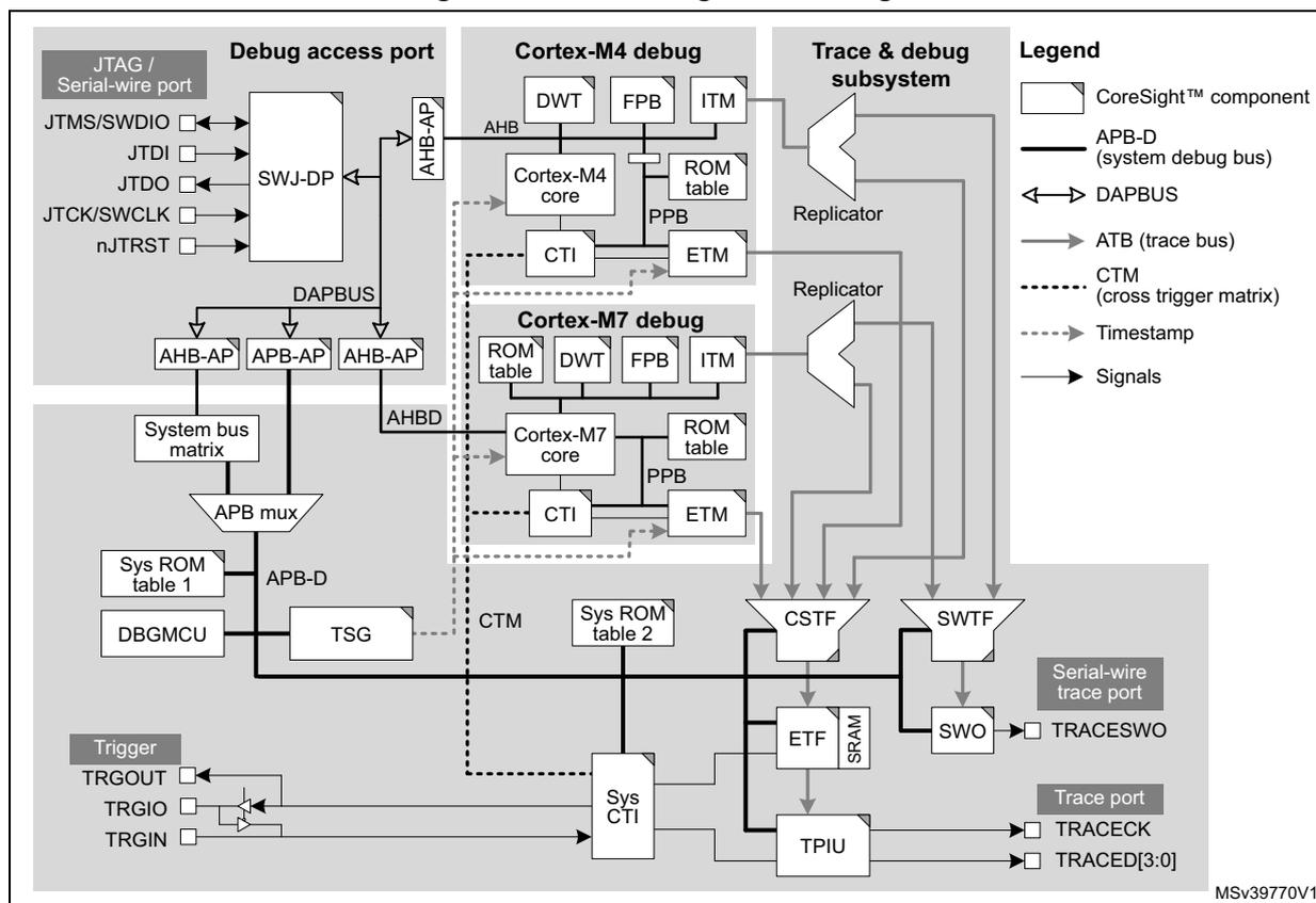
The diagram illustrates the debug infrastructure architecture. On the left, the JTAG/Serial-wire port includes pins JTMS/SWDIO, JTDI, JTDO, JTCK/SWCLK, and nJTRST connected to an SWJ-DP block. This block connects to a Debug access port (DAP) via an AHB-AP. The DAP is connected to a DAPBUS, which in turn connects to three APB-AP blocks (AHB-AP, APB-AP, AHB-AP). These APB-APs connect to a System bus matrix, which is further connected to an APB mux. The APB mux connects to Sys ROM table 1, DBGMCU, and TSG. The TSG connects to a Trigger block with pins TRGOUT, TRGIO, and TRGIN. The Trigger block connects to a Sys CTI block. The Sys CTI block connects to a CTM (cross trigger matrix) and a TPIU. The CTM connects to two Replicator blocks. The Replicator blocks connect to a Trace & debug subsystem, which includes CSTF, SWTF, ETF, SRAM, and TPIU. The TPIU connects to a Trace port with pins TRACECK and TRACED[3:0]. The Trace & debug subsystem also includes a Serial-wire trace port with pin TRACESWO. The Cortex-M4 debug block contains DWT, FPB, ITM, ROM table, PPB, ETM, and CTI components, connected to the Cortex-M4 core via an AHB bus. The Cortex-M7 debug block contains ROM table, DWT, FPB, ITM, ROM table, PPB, ETM, and CTI components, connected to the Cortex-M7 core via an AHBD bus. The Sys ROM table 2 is connected to the TSG and the CTM. A legend on the right defines the symbols: CoreSight™ component (white box), APB-D (system debug bus) (thick line), DAPBUS (double-headed arrow), ATB (trace bus) (single-headed arrow), CTM (cross trigger matrix) (dashed line), Timestamp (dashed line), and Signals (thin line).
63.3.2 Debug infrastructure pins and internal signals
Table 615. JTAG/Serial-wire debug port pins
| Pin name | JTAG debug port | SW debug port | Pin assignment | ||
|---|---|---|---|---|---|
| Type | Description | Type | Description | ||
| JTMS/SWDIO | I | JTAG test mode select | IO | Serial wire data in/out | PA13 |
| JTCK/SWCLK | I | JTAG test clock | I | Serial wire clock | PA14 |
| JTDI | I | JTAG test data input | - | - | PA15 |
| JTDO | O | JTAG test data output | - | - | PB3 |
| nJTRST | I | JTAG test reset | - | - | PB4 |
| Pin name | Type | Description | Pin assignment |
|---|---|---|---|
| TRACED0 | O | Trace synchronous data out 0 | Refer to datasheet |
| TRACED1 | O | Trace synchronous data out 1 | |
| TRACED2 | O | Trace synchronous data out 2 | |
| TRACED3 | O | Trace synchronous data out 3 | |
| TRACECK | O | Trace clock |
| Pin name | Type | Description | Pin assignment |
|---|---|---|---|
| TRACESWO | O | Single wire trace asynchronous data out | PB3 (1) |
- 1. TRACESWO is multiplexed with JTDO. This means that single wire trace is only available when using the serial wire debug interface, not when using JTAG
| Pin name | Type | Description | Pin assignment |
|---|---|---|---|
| TRGIN | I | External trigger input | Refer to datasheet |
| TRGOUT | O | External trigger output | |
| TRGIO | IO | External trigger bi-directional (1) |
- 1. TRGIO can be configured as an input or an output by the TRGOEN bit in the DBGMCU. If configured as an input, it is connected to TRGIN. If an output, it is connected to TRGOUT. This is because TRGIN and TRGOUT are not available on certain packages.
63.3.3 Debug infrastructure powering, clocking and reset
Power domains
Figure 871. Power domains of debug infrastructure
![Figure 871. Power domains of debug infrastructure. This block diagram shows the debug infrastructure components distributed across three power domains: D1, D2, and D3. D3 (top left) contains the JTAG/Serial-wire port (SWJ-DP), DAPBUS, AHB-AP, APB-AP, System bus matrix, APB mux, Sys ROM table 1, DBGMCU, and TSG. D2 (top right) contains the Cortex-M4 core and its associated debug components: DWT, FPB, ITM, ROM table, CTI, and ETM. D1 (bottom) contains the Cortex-M7 core and its associated debug components: ROM table, DWT, FPB, ITM, ROM table, CTI, ETM, and EPPB. Common components include the CTM (cross trigger matrix), Sys CTI, Sys ROM table 2, CSTF, SWTF, ETF, SRAM, and TPIU. The TPIU connects to the Trace port (TRACECK, TRACED[3:0]) and the Serial-wire trace port (TRACESWO). The diagram also includes a legend for CoreSight™ components, APB-D (system debug bus), DAPBUS, ATB (trace bus), CTM (cross trigger matrix), Timestamp, and Signals. The diagram is labeled MSV39772V1.](/RM0399-STM32H745-755-747-757/5eb9e5778008843745a1449142f78b66_img.jpg)
The debug components are distributed across the power domains D1, D2 and D3. The D3 power domain is always considered to be on when the debugger is connected. It therefore contains the SWJ-DP, so that the debugger does not lose the connection with the SoC when one or both of the other power domains are switched off. In addition, it contains the timestamp generator, the DBGMCU and the serial wire trace features. This allows the Cortex-M7 core to be switched off while still allowing basic trace on the Cortex-M4.
The D1 power domain contains the Cortex-M7 core and the associated debug and trace components. It also contains the system trace components located on the APB-D that are common to both processors. This power domain therefore needs to be on whenever a debug access to the Cortex-M7 is required, or whenever a trace functionality is active on either processor.
The D2 domain contains only the debug and trace components dedicated to the Cortex-M4. This power domain can be switched off without any impact on Cortex-M7 debug and trace.
Clock domains
Figure 872. Clock domains of debug infrastructure
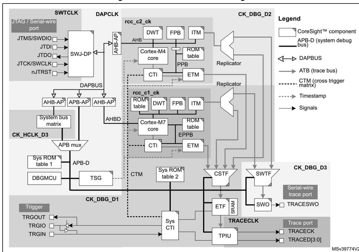
The debugger supplies the clock for the debug port, SWTCLK, via the debug interface pin, JTCK/SWCLK. This clock is used to register the serial input data in both serial wire and JTAG mode, as well as to operate the state machines and internal logic of the debug port. It must therefore continue to toggle for several cycles after the end of an access, to ensure that the debug port returns to the idle state.
The SWJ-DP contains an asynchronous interface to the DAPCLK domain, which covers the rest of the SWJ-DP and the access ports. The DBGMCU, timestamp generator and System ROM table 1 are also in the DAPCLK domain.
CK_DBG_D3 clocks the SWO and serial wire trace funnel.
Both DAPCLK and CK_DBG_D3 are gated versions of the D3 domain system clock (rcc_hclk4).
CK_DBG_D1 clocks the trace components in the D1 power domain: System ROM table 2, CoreSight trace funnel, ETF, system CTI and TPIU. It is a gated version of the D1 domain system clock (rcc_hclk3).
CK_DBG_D2 is the clock for the D2 domain trace bus components. It is a gated version of the D2 domain system clock (rcc_hclk1).
TRACECLK is the trace port output clock. It is derived from the PLL1 R divider output (pll1_r_ck).
All the debug clocks (except DAPCLK) can be enabled and disabled by register bits in the DBGMCU. The DAPCLK domain is enabled by the debugger using the CDBGPWRUPREQ bit in the debug port CTRL/STAT register. The clock must be enabled before the debugger can access any of the debug features on the device. It should be disabled at power up and when the debugger is disconnected, to avoid wasting energy.
The debug and trace components included in the processors (such as ETM ITM, DWG and FPB) are clocked with the corresponding core clock (rcc_c1_ck and rcc_c2_ck).
Debug with low-power modes
The device includes power-saving features allowing individual power domains to be switched off or stopped when not required. If a power domain is switched off or not clocked, all debug components in that domain are inaccessible to the debugger. To avoid this, power saving mode emulation is implemented. If the emulation is enabled for a domain, the domain still enters power saving mode, but its clock and power are maintained. In other words, the domain behaves as if it is in power saving mode, while the debugger does not lose the connection.
The emulation mode is programmed in the MCU Debug (DBGMCU) unit. For more information, refer to Section 63.5.8
Reset of debug infrastructure
The debug components, except for the debug port and access ports, are reset by their respective power domain resets. The debug port (SWJ-DP) is reset by a power-on reset of the D3 domain only.
63.4 Debug access port functional description
The debug access port (DAP) is a debug subsystem comprising serial-wire and JTAG debug port (SWJ-DP) and four access ports.
63.4.1 Serial-wire and JTAG debug port (SWJ-DP)
The SWJ-DP is a CoreSight component that implements an external access port for connecting debugging equipment.
The port can be configured as:
- • a 5-pin standard JTAG debug port (JTAG-DP)
- • a 2-pin (clock + data) “serial-wire” debug port (SW-DP)
The two modes are mutually exclusive, since they share the same IO pins.
By default, the JTAG-DP is selected on system or power-on reset. The five IOs are configured by hardware in debug alternative function mode. The SWJ-DP incorporates pull-up resistors on the JTDI, JTMS/SWDIO, and nJTRST lines, as well as a pull-down resistor on the JTCK/SWCLK line.
A debugger can select the SW-DP by transmitting the following serial data sequence on JTMS/SWDIO:
....,(50 or more ones),...,0,1,1,1,1,0,0,1,1,1,1,0,0,1,1,1,....,(50 or more ones),....
JTCK/SWCLK must be cycled for each data bit.
In SW-DP mode, the unused JTAG lines JTDI, JTDO and nJTRST can be used for other functions.
All SWJ port IOs can be reconfigured to other functions by software, in which case debugging is no longer possible.
Serial wire debug port
The Serial wire debug protocol uses two pins:
- • SWCLK: clock from host to target
- • SWDIO: bi-directional serial data (100k \( \Omega \) pull-up required)
Serial data is transferred LSB first, synchronously with the clock. A transfer comprises three phases:
- 1. packet request (8 bits) transmitted by the host
- 2. acknowledge response (3 bits) transmitted by the target
- 3. data transfer (33 bits) transmitted by the host (in the case of a write) or target (in the case of a read)
The data transfer only occurs if the acknowledge response is OK.
If the direction of the data is reversed between each phase, a single clock cycle turn-around time is inserted.
Table 619. Packet request
| Field bits | Name | Description |
|---|---|---|
| 0 | Start | Must be "1" |
| 1 | APnDP | 0: DP register access - see
Table 623
for a list of DP registers 1: AP register access - see Section 63.4.2 |
| 2 | RnW | 0: Write request 1: Read request |
| 4:3 | A(3:2) | Address field of the DP or AP register (refer to Table 623 and Table 624 ) |
| 5 | Parity | Single bit parity of preceding bits |
| 6 | Stop | 0 |
| 7 | Park | Not driven by host. Must be read as "1" by target. |
Table 620. ACK response
| Field bits | Name | Description |
|---|---|---|
| 2:0 | ACK | 000b: FAULT 010b: WAIT 100b: OK |
Table 621. Data transfer
| Bit field | Name | Description |
|---|---|---|
| 31:0 | WDATA or RDATA | Write or Read data |
| 32 | Parity | Single bit parity of 32 data bits |
Figure 873 shows successful write and read transfers.
Figure 873. SWD successful data transfer
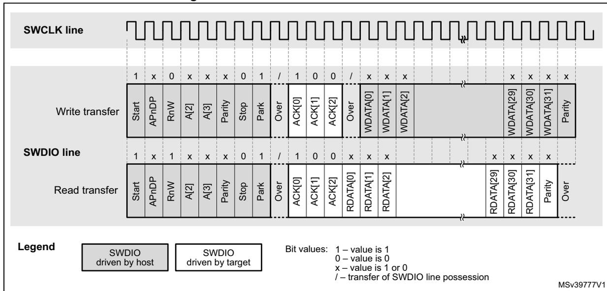
Legend
- SWDIO driven by host (light gray box)
- SWDIO driven by target (white box)
Bit values:
- 1 – value is 1
- 0 – value is 0
- x – value is 1 or 0
- / – transfer of SWDIO line possession
MSv39777V1
For any FAULT or WAIT ACK response from the target, the data transfer phase is canceled, unless overrun detection is enabled, in which case the data will be ignored by the target (in the case of a write), or not driven (in the case of a read).
A line reset must be generated by the host when it is first connected, or following a protocol error. The line reset consists of 50 or more SWCLK cycles with SWDIO high, followed by two SWCLK cycles with SWDIO low.
For more details on the Serial Wire debug protocol, refer to the Arm® Debug Interface Architecture Specification [1].
Note: The SWJ-DP implements SWD protocol version 2.
JTAG debug port
Figure 874. JTAG TAP state machine
stateDiagram-v2
    [*] --> Test-Logic-Reset: JTMS=1
    Test-Logic-Reset --> Run-Test/Idle: JTMS=0
    Run-Test/Idle --> Select-DR-Scan: JTMS=1
    Run-Test/Idle --> Select-IR-Scan: JTMS=1
    Select-DR-Scan --> Capture-DR: JTMS=0
    Select-DR-Scan --> Select-IR-Scan: JTMS=1
    Select-IR-Scan --> Capture-IR: JTMS=0
    Select-IR-Scan --> Select-DR-Scan: JTMS=1
    Capture-DR --> Shift-DR: JTMS=0
    Capture-DR --> Exit1-DR: JTMS=1
    Shift-DR --> Shift-DR: JTMS=0
    Shift-DR --> Exit1-DR: JTMS=1
    Exit1-DR --> Pause-DR: JTMS=0
    Exit1-DR --> Select-DR-Scan: JTMS=1
    Pause-DR --> Pause-DR: JTMS=0
    Pause-DR --> Exit2-DR: JTMS=1
    Exit2-DR --> Update-DR: JTMS=0
    Exit2-DR --> Select-DR-Scan: JTMS=1
    Update-DR --> Run-Test/Idle: JTMS=0
    Update-DR --> Select-IR-Scan: JTMS=1
    Capture-IR --> Shift-IR: JTMS=0
    Capture-IR --> Exit1-IR: JTMS=1
    Shift-IR --> Shift-IR: JTMS=0
    Shift-IR --> Exit1-IR: JTMS=1
    Exit1-IR --> Pause-IR: JTMS=0
    Exit1-IR --> Select-IR-Scan: JTMS=1
    Pause-IR --> Pause-IR: JTMS=0
    Pause-IR --> Exit2-IR: JTMS=1
    Exit2-IR --> Update-IR: JTMS=0
    Exit2-IR --> Select-IR-Scan: JTMS=1
    Update-IR --> Run-Test/Idle: JTMS=0
    Update-IR --> Select-DR-Scan: JTMS=1
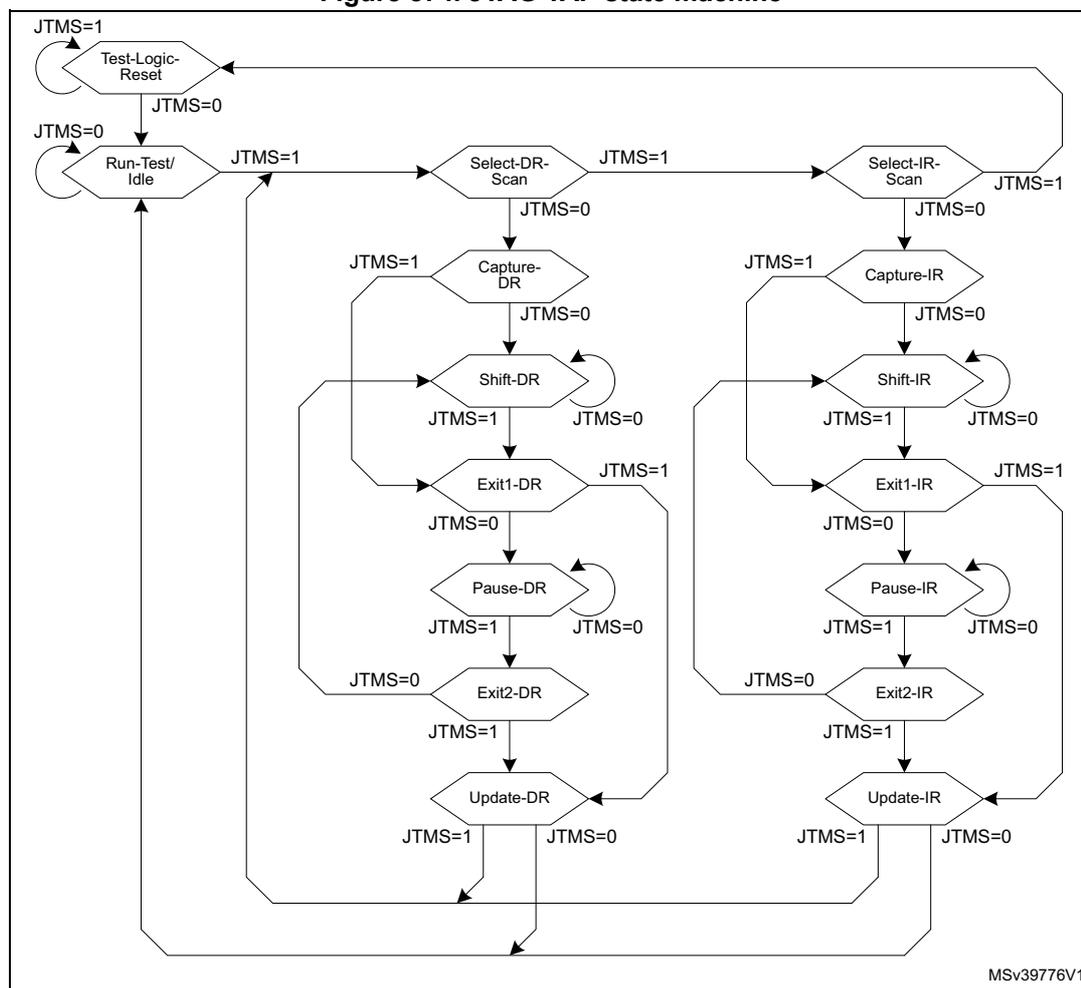
The JTAG-DP implements a TAP state machine (TAPSM) based on IEEE 1149.1-1990. The state machine is shown in Figure 874. It controls two scan chains, one associated with an instruction register (IR) and one with a number of data registers (DR).
When the TAPSM goes through the Capture-IR state, 0b0001 is transferred to the instruction register (IR) scan chain. The IR scan chain is connected between JTDI and JTDO.
While the TAPSM is in the Shift-IR state, the IR scan chain shifts one bit for each rising edge of JTCK. This means that on the first tick:
- • The LSB of the IR scan chain is output on JTDO.
- • Bit [n] of the IR scan chain is transferred to bit [n-1].
- • The value on JTDI is transferred to the MSB of the IR scan chain.
When the TAPSM goes through the Update-IR state, the value scanned in the IR scan chain is transferred to the instruction register.
When the TAPSM goes through the Capture-DR state, a value is transferred from one of the data registers onto one of the DR scan chains, connected between JTDI and JTDO.
The value held in the instruction register determines which data register, and associated DR scan chain, is selected.
This data is then shifted while the TAPSM is in the Shift-DR state, in the same way as the IR shift in the Shift-IR state.
When the TAPSM goes through the Update-DR state, the value scanned in the DR scan chain is transferred to the selected data register.
When the TAPSM is in the Run-Test/Idle state, no special actions occur. The IDCODE instruction is loaded in IR.
When active, the nJTRST signal resets the state machine asynchronously to the Test-Logic-Reset state.
The data registers corresponding to the 4-bit IR instructions are listed in Table 622 .
Table 622. JTAG-DP data registers
| Instruction register | Data register | Scan chain length | Description |
|---|---|---|---|
| 0000 to 0111 | (BYPASS) | 1 | Not implemented: BYPASS selected |
| 1000 | ABORT | 35 | Abort register – Bits 31:1 = reserved – Bit 0 = APABORT: write 1 to generate an AP abort |
| 1001 | (BYPASS) | 1 | Reserved: BYPASS selected |
| 1010 | DPACC | 35 | Debug port access register Initiates the debug port and allows access to a debug port register. – When transferring data IN: Bits 34:3 = DATA[31:0] = 32-bit data to transfer for a write request Bits 2:1 = A[3:2] = 2-bit address of a debug port register. Bit 0 = RnW = Read request (1) or write request (0). – When transferring data OUT: Bits 34:3 = DATA[31:0] = 32-bit data which is read following a read request Bits 2:0 = ACK[2:0] = 3-bit Acknowledge: 010b = OK/FAULT 001b = WAIT Others: reserved |
Table 622. JTAG-DP data registers (continued)
| Instruction register | Data register | Scan chain length | Description |
|---|---|---|---|
| 1011 | APACC | 35 | Access port access register Initiates an access port and allows access to an access port register. – When transferring data IN: Bits 34:3 = DATA[31:0] = 32-bit data to shift in for a write request Bits 2:1 = A[3:2] = 2-bit sub-address of an access port register. Bit 0 = RnW= Read request (1) or write request (0). – When transferring data OUT: Bits 34:3 = DATA[31:0] = 32-bit data which is read following a read request Bits 2:0 = ACK[2:0] = 3-bit Acknowledge: 010b = OK/FAULT 001b = WAIT OTHER = reserved |
| 1100 | (BYPASS) | 1 | Reserved: BYPASS selected |
| 1101 | (BYPASS) | 1 | Reserved: BYPASS selected |
| 1110 | IDCODE | 32 | ID Code 0x6BA0 0477: Arm® JTAG debug port ID code |
| 1111 | BYPASS | 1 | Bypass A single JTCCK cycle delay is inserted between JTDI and JTDO |
The DR registers are described in more detail in the Arm® Debug Interface Architecture Specification [1].
Debug port registers
The SW-DP and JTAG-DP both access the debug port (DP) registers. These are listed in Table 623.
The debugger can access the DP registers as follows:
- 1. Program the SELECT register DPBANKSEL field in the DP to select the register bank to be accessed (see Table 623)
- 2. Program the A(3:2) field in the DPACC register, if using JTAG, with the register address within the bank. Program the R/W bit to select a read or a write. In the case of a write, program the DATA field with the write data. If using SWD, the A(3:2) and R/W fields are part of the Packet Request word sent to the SW-DP with the APnDP bit reset (see Table 619). The write data is sent in the data phase.
Table 623. Debug port registers
| Address | A(3:2) field value | R/W | Description |
|---|---|---|---|
| 0x0 | 00 | R | DP_PIDR register (2) . It contains the IDCODE for the debug port. |
| W | DP_ABORT register (1) . It aborts the current AP transaction. This register is also used to clear the error flags in the DP_CTRL/STAT register. | ||
| 0x4 | 01 | R/W | If DPBANKSEL[3:0] = 0x0 (DP_SELECT register): CTRL/STAT register. It controls the DP and provides status information. |
| If DPBANKSEL[3:0] = 0x1 (DP_SELECT register): DP_DLCR register (2) . It controls the operating mode of the SWD Data Link. | |||
| If DPBANKSEL[3:0] = 0x2 (DP_SELECT register): DP_TARGETID register. It provides target identification information. | |||
| If DPBANKSEL[3:0] = 0x3 (DP_SELECT register): DLPIDR register (2) . It provides the SWD protocol version. | |||
| 0x8 | 10 | R | RESEND register (2) . It returns the value that was returned by the last AP read or DP_RDBUFF read, used in the event of a corrupted read transfer. |
| W | DP_SELECT register. It selects the access port, access port register bank, and DP register at address 0x4. | ||
| 0xC | 11 | R | DP_RDBUFF register Via JTAG-DP, it enables the debugger to get the final result after a sequence of operations (without requesting new JTAG-DP operation). Via SW-DP, it contains the result of the preceding AP read access, allowing a new AP access to be avoided. |
| W | DP_TARGETSEL register
(2)
. On a write to DP_TARGETSEL immediately following a line reset sequence, the target is selected if the following conditions are both met: – Bits [31:28] match bits [31:28] in the DP_DLPIDR register. – Bits [27:0] match bits [27:0] in the DP_TARGETID register. Writing any other value deselects the target. Debug tools must write 0xFFFFFFFF to deselect all targets. This is an invalid DP_TARGETID value. All other invalid DP_TARGETID values are reserved. |
- 1. Access to the AP ABORT register from the JTAG-DP is done using the ABORT instruction.
- 2. Only accessible via SW-DP. Register is “reserved” via JTAG-DP.
Debug port identification register (DP_PIDR)
Address offset: 0x00
Reset value: 0x6BA0 2477
| 31 | 30 | 29 | 28 | 27 | 26 | 25 | 24 | 23 | 22 | 21 | 20 | 19 | 18 | 17 | 16 |
|---|---|---|---|---|---|---|---|---|---|---|---|---|---|---|---|
| REVISION[3:0] | PARTNO[7:0] | Res. | Res. | Res. | MIN | ||||||||||
| r | r | r | r | r | r | r | r | r | r | r | r | r | |||
| 15 | 14 | 13 | 12 | 11 | 10 | 9 | 8 | 7 | 6 | 5 | 4 | 3 | 2 | 1 | 0 |
| VERSION[3:0] | DESIGNER[10:0] | Res. | |||||||||||||
| r | r | r | r | r | r | r | r | r | r | r | r | r | r | r | |

Bits 31:28 REVISION[3:0] : Revision code
0x6
Bits 27:20 PARTNO[7:0] : Debug port part number
0xBA
Bits 19:17 Reserved, must be kept at reset value.
Bit 16 MIN : Minimal debug port (MINDP) implementation
0: MINDP not implemented (transaction counter and pushed operations are supported)
Bits 15:12 VERSION[3:0] : DP architecture version
0x2: DPv2
Bits 11:1 DESIGNER[10:0] : JEDEC designer identity code
0x23B: Arm ®
Bit 0 Reserved, must be kept at reset value.
Debug port abort register (DP_ABORT)
Address offset: 0x0
Reset value: 0x0000 0000
| 31 | 30 | 29 | 28 | 27 | 26 | 25 | 24 | 23 | 22 | 21 | 20 | 19 | 18 | 17 | 16 |
|---|---|---|---|---|---|---|---|---|---|---|---|---|---|---|---|
| Res. | Res. | Res. | Res. | Res. | Res. | Res. | Res. | Res. | Res. | Res. | Res. | Res. | Res. | Res. | Res. |
| 15 | 14 | 13 | 12 | 11 | 10 | 9 | 8 | 7 | 6 | 5 | 4 | 3 | 2 | 1 | 0 |
| Res. | Res. | Res. | Res. | Res. | Res. | Res. | Res. | Res. | Res. | Res. | ORUNERRCLR | WDERRCLR | STKERRCLR | STKCOMPCLR | DAPABORT |
| w | w | w | w | w |
Bits 31:5 Reserved, must be kept at reset value.
Bit 4 ORUNERRCLR : Overrun error clear bit
0: No effect
1: Clear CTRL/STAT register's STICKYORUN bit
Bit 3 WDERRCLR : Write data error clear bit
0: No effect
1: Clear CTRL/STAT register's WDATAERR bit
Bit 2 STKERRCLR : Sticky error clear bit
0: No effect
1: Clear CTRL/STAT register's STICKYERR bit
Bit 1 STKCMPCLR : Sticky compare clear bit
0: No effect
1: Clear CTRL/STAT register's STICKYCMP bit
Bit 0 DAPABORT : Abort current AP transaction
The transaction is aborted if an excessive number of WAIT responses are returned, indicating that the transaction has stalled.
0: No effect
1: Abort transaction
Debug port control/status register (DP_CTRL/STAT)
Address offset: 0x4
Reset value: 0x0000 0000
| 31 | 30 | 29 | 28 | 27 | 26 | 25 | 24 | 23 | 22 | 21 | 20 | 19 | 18 | 17 | 16 |
|---|---|---|---|---|---|---|---|---|---|---|---|---|---|---|---|
| CSYSPWRUPACK | CSYSPWRUPREQ | CDBGPWRUPACK | CDBGPWRUPREQ | CDBGIRSTACK | CDBGIRSTREQ | Res. | Res. | TRNCNT[11:4] | |||||||
| 1 | rw | r | rw | r | rw | rw | rw | rw | rw | rw | rw | rw | rw | ||
| 15 | 14 | 13 | 12 | 11 | 10 | 9 | 8 | 7 | 6 | 5 | 4 | 3 | 2 | 1 | 0 |
| TRNCNT[3:0] | MASKLANE[3:0] | WDATAERR | READOK | STICKYERR | STICKYCMP | TRNMODE[1:0] | STICKYORUN | ORUNDETECT | |||||||
| rw | rw | rw | rw | rw | rw | rw | rw | r | r | rw | w | w | w | w | w |
Bit 31 CSYSPWRUPACK : System domain power-up status bit - not used in this device
Bit 30 CSYSPWRUPREQ : System domain power-up control bit - not used in this device
Bit 29 CDBGPWRUPACK : Debug domain power-up status bit
This bit is read-only. It returns the status of the debug domain power-up acknowledge signal from the power controller.
0: domain powered down
1: domain powered up
Bit 28 CDBGPWRUPREQ : Debug domain power-up/down control bit
This bit controls the debug domain power-up/down request signal to the power controller.
0: power-down requested
1: power-up requested
Bit 27 CDBGIRSTACK : Debug domain reset status bit - not used in this device
Bit 26 CDBGIRSTREQ : Debug domain reset control bit - not used in this device
Bits 25:24 Reserved, must be kept at reset value.
Bits 23:12 TRNCNT[11:0] : Transaction counter
To program a sequence of transactions to incremental addresses via an AP, TRNCNT bits are loaded with the number of transactions to perform. It is decremented on successful completion of each transaction.
Bits 11:8 MASKLANE[3:0] : Pushed-compare and pushed-verify masking bits
The field indicates the bytes to be masked in pushed-compare and pushed-verify operations (DP_CTRL/STAT register's field TRNMODE = 1 or 2). In the pushed operations, the word supplied in an AP write transaction is compared with the current value at the target AP address.
0b1XXX: include byte lane 3 in comparisons
0bX1XX: include byte lane 2 in comparisons
0bXX1X: include byte lane 1 in comparisons
0bXXX1: include byte lane 0 in comparisons
Bit 7 WDATAERR : Write data error in SW-DP
The bit indicates
- – a parity or a framing error on the data phase of a write operation, or
- – a write operation that had been accepted by the DP has then been discarded without being submitted to the AP
This bit is read-only. It is reset by writing 1 to the WDERRCLR bit of the DP_ABORT register.
0: No error
1: Error has occurred
This bit is reserved in JTAG-DP.
Bit 6 READOK : AP read response in SW-DP
This bit indicates the response to the last AP read access. It is read-only.
0: Read not OK
1: Read OK
This bit is Reserved in JTAG-DP.
Bit 5 STICKYERR : Transaction error (read-only in SW-DP, R/W in JTAG-DP)
This bit indicates that an error occurred during an AP transaction.
0: No error
1: Error has occurred
In the SW-DP, this bit is reset by writing 1 to the STKERRCLR bit of the DP_ABORT register.
In the JTAG-DP, this bit is reset by programming it to 1.
Bit 4 STICKYCMP : Compare match (read-only in SW-DP, R/W in JTAG-DP)
This bit indicates that a match occurred in a pushed operation.
0: Match if TRNMODE = 0x1; no match if TRNMODE = 0x2
1: No match if TRNMODE = 0x1; match if TRNMODE = 0x2
In the SW-DP, this bit is reset by writing 1 to the STKCMPCLR bit in the DP_ABORT register.
In the JTAG-DP, this bit is reset by programming it to 1.
Bits 3:2 TRNMODE[1:0] : Transfer mode for AP write operations
For read operations, this field must be set to 0x0.
0x0: Normal operation - AP transactions are passed directly to the AP.
0x1: Pushed-verify operation. The DP stores the write data and performs a read transaction at the target AP address. The result of the read operation is compared with the stored data. If they do not match, the STICKYCMP bit is set.
0x2: Pushed-compare operation. The DP stores the write data and performs a read transaction at the target AP address. The result of the read is compared with the stored data. If they match, the STICKYCMP bit is set.
0x3: Reserved
In pushed operations, only the data bytes indicated by the MASKLANE field are included in the comparison.
Bit 1 STICKYORUN : Overrun (read-only in SW-DP, R/W in JTAG-DP)
This bit indicates that an overrun occurred (new transaction received before previous transaction completed). This bit is only set if the ORUNDETECT bit is set.
0: No overrun
1: Overrun occurred
In the SW-DP, this bit is reset by writing 1 to the ABORT register's ORUNERRCLR bit. In the JTAG-DP, this bit is reset by writing a 1 to it.
Bit 0 ORUNDETECT : Overrun detection mode enable
0: Overrun detection disabled
1: Overrun detection enabled. In the event of an overrun, the STICKYORUN bit is set and subsequent transactions are blocked until the STICKYORUN bit is cleared.
Debug port data link control register (DP_DLCR)
Address offset: 0x4
Reset value: 0x0000 0040
| 31 | 30 | 29 | 28 | 27 | 26 | 25 | 24 | 23 | 22 | 21 | 20 | 19 | 18 | 17 | 16 |
|---|---|---|---|---|---|---|---|---|---|---|---|---|---|---|---|
| Res. | Res. | Res. | Res. | Res. | Res. | Res. | Res. | Res. | Res. | Res. | Res. | Res. | Res. | Res. | Res. |
| 15 | 14 | 13 | 12 | 11 | 10 | 9 8 | 7 | 6 | 5 | 4 | 3 | 2 | 1 | 0 | |
| Res. | Res. | Res. | Res. | Res. | Res. | TURNROUND[1:0] | Res. | Res. | Res. | Res. | Res. | Res. | Res. | Res. | |
| rw | rw | ||||||||||||||
Bits 31:10 Reserved, must be kept at reset value.
Bits 9:8 TURNROUND[1:0] : Tristate period for SWDIO
0x0: 1 data bit period
0x1: 2 data bit periods
0x2: 3 data bit periods
0x3: 4 data bit periods
Bits 7:0 Reserved, must be kept at reset value.
Debug port target identification register (DP_TARGETID)
Address offset: 0x4
Reset value: 0x0450 0041
| 31 | 30 | 29 | 28 | 27 | 26 | 25 | 24 | 23 | 22 | 21 | 20 | 19 | 18 | 17 | 16 |
|---|---|---|---|---|---|---|---|---|---|---|---|---|---|---|---|
| TREVISION[3:0] | TPARTNO[15:4] | ||||||||||||||
| r | r | r | r | r | r | r | r | r | r | r | r | r | r | r | r |
| 15 | 14 | 13 | 12 | 11 | 10 | 9 | 8 | 7 | 6 | 5 | 4 | 3 | 2 | 1 | 0 |
| TPARTNO[3:0] | TDESIGNER[10:0] | Res. | |||||||||||||
| r | r | r | r | r | r | r | r | r | r | r | r | r | r | r | |
Bits 31:28 TREVISION[3:0] : Target revision
0x0: revision 0
Bits 27:12 TPARTNO[15:0] : Target part number
0x4500: STM32H7
Bits 11:1 TDESIGNER[10:0] : Target designer JEDEC code
0x020: STMicroelectronics
Bit 0 Reserved, set to 1.
Debug port data link protocol identification register (DP_DLPIDR)
Address offset: 0x4
Reset value: 0x0000 0001
| 31 | 30 | 29 | 28 | 27 | 26 | 25 | 24 | 23 | 22 | 21 | 20 | 19 | 18 | 17 | 16 |
|---|---|---|---|---|---|---|---|---|---|---|---|---|---|---|---|
| TINSTANCE[3:0] | Res. | Res. | Res. | Res. | Res. | Res. | Res. | Res. | Res. | Res. | Res. | Res. | |||
| r | r | r | r | ||||||||||||
| 15 | 14 | 13 | 12 | 11 | 10 | 9 | 8 | 7 | 6 | 5 | 4 | 3 | 2 | 1 | 0 |
| Res. | Res. | Res. | Res. | Res. | Res. | Res. | Res. | Res. | Res. | Res. | Res. | PROTSVN[3:0] | |||
| r | r | r | r | ||||||||||||
Bits 31:28 TINSTANCE[3:0] : Target instance number
These bits define the instance number for this device in a multi-drop system.
0x0
Bits 27:4 Reserved, must be kept at reset value.
Bits 3:0 PROTSVN[3:0] : Serial Wire Debug protocol version
0x1: Version 2
Debug port resend register (DP_RESEND)
Address offset: 0x8
Reset value: 0x0000 0000
| 31 | 30 | 29 | 28 | 27 | 26 | 25 | 24 | 23 | 22 | 21 | 20 | 19 | 18 | 17 | 16 |
|---|---|---|---|---|---|---|---|---|---|---|---|---|---|---|---|
| RESEND[31:16] | |||||||||||||||
| r | r | r | r | r | r | r | r | r | r | r | r | r | r | r | r |
| 15 | 14 | 13 | 12 | 11 | 10 | 9 | 8 | 7 | 6 | 5 | 4 | 3 | 2 | 1 | 0 |
| RESEND[15:0] | |||||||||||||||
| r | r | r | r | r | r | r | r | r | r | r | r | r | r | r | r |
Bits 31:0 RESEND[31:0] : Last AP read or DP RDBUFF read value
These bits contain the value that was returned by the last AP read or DP RDBUFF read.
Used in the event of a corrupted read transfer.
Debug port access port select register (DP_SELECT)
Address offset: 0x8
Reset value: 0xXXXX XXXX
| 31 | 30 | 29 | 28 | 27 | 26 | 25 | 24 | 23 | 22 | 21 | 20 | 19 | 18 | 17 | 16 |
|---|---|---|---|---|---|---|---|---|---|---|---|---|---|---|---|
| APSEL[3:0] | Res. | Res. | Res. | Res. | Res. | Res. | Res. | Res. | Res. | Res. | Res. | Res. | |||
| w | w | w | w | ||||||||||||
| 15 | 14 | 13 | 12 | 11 | 10 | 9 | 8 | 7 | 6 | 5 | 4 | 3 | 2 | 1 | 0 |
| Res. | Res. | Res. | Res. | Res. | Res. | Res. | Res. | APBANKSEL[3:0] | DPBANKSEL[3:0] | ||||||
| w | w | w | w | w | w | w | w | ||||||||
Bits 31:28 APSEL[3:0] : Access port select bits
These bits select the access port for the next transaction.
0x0: AP0 - Cortex-M7 debug access port (AHB-AP)
0x1: AP1 - D3 access port (AHB-AP)
0x2: AP2 - System debug access port (APB-AP)
0x3: AP3 - Cortex-M4 debug access port (AHB-AP)
0x4 to 0xF: Reserved
Bits 27:8 Reserved, must be kept at reset value.
Bits 7:4 APBANKSEL[3:0] : AP register bank select bits
These bits select the 4-word register bank on the active AP for the next transaction.
Bits 3:0 DPBANKSEL[3:0] : DP register bank select bits
These bits select the register at address 0x4 of the debug port.
0x0: CTRL/STAT register
0x1: DLCR register
0x2: TARGETID register
0x3: DLPIDR register
0x4 to 0xF: Reserved
Debug port read buffer register (DP_RDBUFF)
Address offset: 0xC
Reset value: 0x0000 0000
| 31 | 30 | 29 | 28 | 27 | 26 | 25 | 24 | 23 | 22 | 21 | 20 | 19 | 18 | 17 | 16 |
| RDBUFF[31:16] | |||||||||||||||
| r | r | r | r | r | r | r | r | r | r | r | r | r | r | r | r |
| 15 | 14 | 13 | 12 | 11 | 10 | 9 | 8 | 7 | 6 | 5 | 4 | 3 | 2 | 1 | 0 |
| RDBUFF[15:0] | |||||||||||||||
| r | r | r | r | r | r | r | r | r | r | r | r | r | r | r | r |
Bits 31:0 RDBUFF[31:0] : Last AP read value
The field contains the value returned by the last AP read access. There are two ways to retrieve the value returned by an AP read access:
- – perform a second read access to the same address, which initiates a new transaction on the corresponding bus, or
- – read the value returned by the last AP read access from the DP_RDBUFF register, in which case no new AP transaction occurs
Debug port target identification register (DP_TARGETSEL)
Address offset: 0xC
Reset value: N/A
| 31 | 30 | 29 | 28 | 27 | 26 | 25 | 24 | 23 | 22 | 21 | 20 | 19 | 18 | 17 | 16 |
|---|---|---|---|---|---|---|---|---|---|---|---|---|---|---|---|
| TINSTANCE[3:0] | TPARTNO[15:4] | ||||||||||||||
| w | w | w | w | w | w | w | w | w | w | w | w | w | w | w | w |
| 15 | 14 | 13 | 12 | 11 | 10 | 9 | 8 | 7 | 6 | 5 | 4 | 3 | 2 | 1 | 0 |
| TPARTNO[3:0] | TDESIGNER[10:0] | Res. | |||||||||||||
| w | w | w | w | w | w | w | w | w | w | w | w | w | w | w | |
Bits 31:28 TINSTANCE[3:0] : Target instance number
The field defines the instance number for the target device in a multi-drop system. It must be programmed with the same value as TINSTANCE field of DP_DLPIDR register, in order to select this device.
Bits 27:12 TPARTNO[15:0] : Target part number
The field defines the part number for the target device. It must be programmed with the same value as TPARTNO field of DP_TARGETID register, in order to select this device.
Bits 11:1 TDESIGNER[10:0] : Target designer JEDEC code
The field defines the JEDEC code for the target device. It must be programmed with the same value as TDESIGNER field of DP_TARGETID register, in order to select this device.
Bit 0 Reserved, must be kept at reset value.
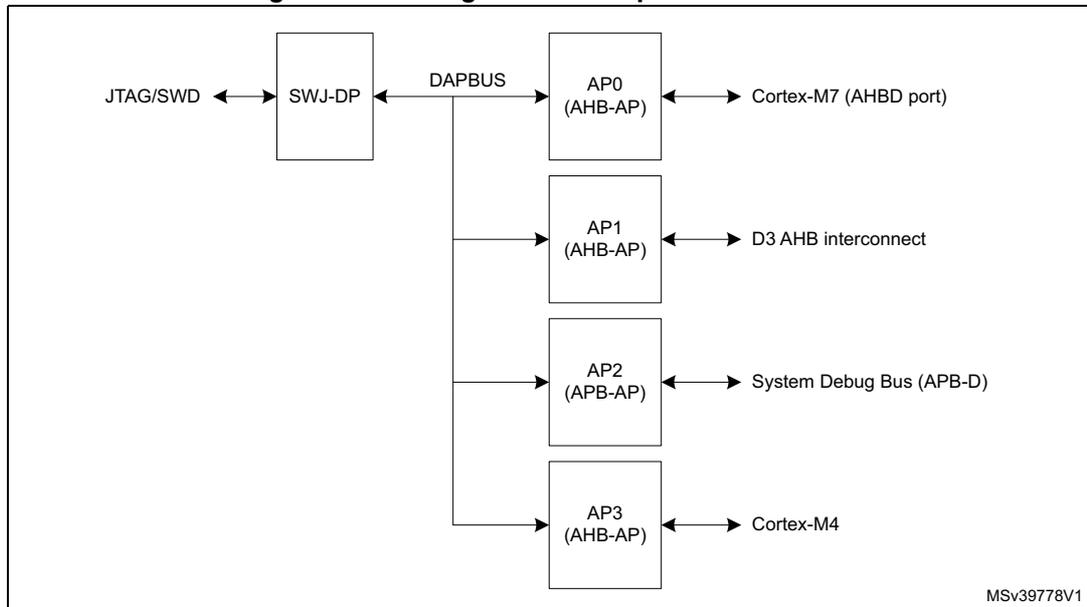
63.4.2 Access ports
Figure 875. Debug and access port connections
    graph LR
      JTAG_SWD[JTAG/SWD] <--> SWJ_DP[SWJ-DP]
      SWJ_DP <--> DAPBUS[DAPBUS]
      DAPBUS --> AP0[AP0
(AHB-AP)]
      DAPBUS --> AP1[AP1
(AHB-AP)]
      DAPBUS --> AP2[AP2
(APB-AP)]
      DAPBUS --> AP3[AP3
(AHB-AP)]
      AP0 <--> CortexM7[Cortex-M7 (AHBD port)]
      AP1 <--> D3AHB[D3 AHB interconnect]
      AP2 <--> SystemDebugBus[System Debug Bus (APB-D)]
      AP3 <--> CortexM4[Cortex-M4]
The access ports (AP) attached to the DP as the following:
- 1. AP0: Cortex-M7 access port (AHB-AP). Allows access to the debug and trace features integrated in the Cortex-M7 processor core via an AHB-Lite bus connected to the AHBD port of the processor.
- 2. AP1: D3 access port (AHB-AP). Allows access to the bus matrix in the D3 domain. This gives visibility of the D3 domain memory and peripherals when the D1 and D2 domains are switched off. No CoreSight components are accessible via this port.
- 3. AP2: System access port (APB-AP). Allows access to the debug and trace features on the system APB debug bus, that is, all components not included in one of the processor cores.
- 4. AP3: Cortex-M4 access port (AHB-AP). Allows access to the debug and trace features integrated in the Cortex-M4 processor core via its internal AHB bus.
All access ports are of MEM-AP type, that is, the debug and trace component registers are mapped in the address space of the associated debug bus. The AP is seen by the debugger as a set of 32-bit registers organized in banks of four registers each. Some of these registers are used to configure or monitor the AP itself, while others are used to perform a transfer on the bus. The AP registers are listed in Table 624 .
The address of the AP registers is composed of:
- • bits [7:4]: content of the DP_SELECT register's APBANKSEL field
- • bits [3:2]: content of the A(3:2) field of the APACC data register in the JTAG-DP (see Table 622 ) or of the SW-DP Packet Request (see Table 619 ), depending on the debug interface used
- • bits [1:0]: Always set to 0
The content of the SELECT register APSEL field in the DP define which MEM-AP is being accessed.
The debugger can access the AP registers as follows:
- 1. Program the DP_SELECT register's APSEL field to choose one of the APs, and the APBANKSEL field to select the register bank to be accessed.
- 2. Program the A(3:2) field in the APACC register, if using JTAG, with the register address within the bank. Program the RnW bit to select a read or a write. In the case of a write, program the DATA field with the write data. If using SWD, the A(3:2) and RnW fields are part of the Packet Request word sent to the SW-DP with the APnDP bit set (see Table 619 ). The write data is sent in the data phase.
The debugger can access the memory mapped debug component registers through the MEM-AP registers (using the AP register access procedure described above) as follows:
- 1. Program the transaction target address in the TAR register.
- 2. Program the CSW register, if necessary, with the transfer parameters (AddrInc for example).
- 3. Write to or read from the DRW register to initiate a bus transaction at the address held in the TAR register. Alternatively, a read or write to banked data register B n triggers an access to address TAR[31:4] + n (this allows accessing up to four consecutive addresses without changing the address in the TAR register).
For more detailed information on the MEM-AP, refer to the Arm ® Debug Interface Architecture Specification [1] . To use the MEM-AP to connect the debug port to the debug components (in the example, a processor, an ETM and a ROM table), go to Section 63.6.2 :
Cortex-M7 data watchpoint and trace unit (DWT) and Section 63.7.2: Cortex-M4 data watchpoint and trace unit (DWT).
MEM-AP registers
Table 624. MEM-AP registers
| Address | APBANKSEL | A(3:2) | Name | Description |
|---|---|---|---|---|
| 0x00 | 0x0 | 0 | AP_CSW | Control/status word register |
| 0x04 | 0x0 | 1 | AP_TAR | Transfer address register Target address for the bus transaction. |
| 0x08 | - | - | - | Reserved |
| 0x0C | 0x0 | 3 | AP_DRW | Data read/write register Access to this register triggers a corresponding transaction on the debug bus to the address in TAR[31:0] |
| 0x10 | 0x1 | 0 | AP_BD0 | Banked data 0 register Access to this register triggers a corresponding transaction on the debug bus to the address in TAR[31:4] << 4 + 0x0 |
| 0x14 | 0x1 | 1 | AP_BD1 | Banked Data 1 register Access to this register triggers a corresponding transaction on the debug bus to the address in TAR[31:4] << 4 + 0x4 |
| 0x18 | 0x1 | 2 | AP_BD2 | Banked data 2 register Access to this register triggers a corresponding transaction on the debug bus to the address in TAR[31:4] << 4 + 0x8 |
| 0x1C | 0x1 | 3 | AP_BD3 | Banked data 3 register Access to this register triggers a corresponding transaction on the debug bus to the address in TAR[31:4] << 4 + 0xC |
| 0x20-0xEC | - | - | - | Reserved |
| 0xF0 | - | - | - | Reserved |
| 0xF4 | - | - | - | Reserved |
| 0xF8 | 0xF | 2 | AP_BASE | Debug base address register (RO) Base address of the ROM table |
| 0xFC | 0xF | 3 | AP_IDR | Identification register (RO) |
Access port control/status word register (AP_CSW)
Address offset: 0x0
Reset value: 0x0000 0002 (APB-AP), 0x4000 0002 (AHB-AP)
| 31 | 30 | 29 | 28 | 27 | 26 | 25 | 24 | 23 | 22 | 21 | 20 | 19 | 18 | 17 | 16 |
|---|---|---|---|---|---|---|---|---|---|---|---|---|---|---|---|
| Res. | SPROT | Res. | PROT[4:0] | SPISTA TUS | Res. | Res. | Res. | Res. | Res. | Res. | Res. | ||||
| rw | rw | rw | rw | rw | rw | r | |||||||||
| 15 | 14 | 13 | 12 | 11 | 10 | 9 | 8 | 7 | 6 | 5 | 4 | 3 | 2 | 1 | 0 |
| Res. | Res. | Res. | Res. | MODE[3:0] | TRINP ROG | DEVIC EEN | ADDRINC[1:0] | Res. | SIZE[2:0] | ||||||
| rw | rw | rw | rw | r | r | rw | rw | rw | rw | rw | |||||
Bit 31 Reserved, must be kept at reset value.
Bit 30 SPROT : Secure transfer request bit
In the APB-AP, this field is reserved. In the AHB-APs, this field sets the protection attribute HPROT[6] of the bus transfer.
0: If SPIDEN is high, secure transfer. If SPIDEN is low, non-secure transfer.
1: Non-secure transfer.
Bit 29 Reserved, must be kept at reset value.
Bits 28:24 PROT[4:0] Bus transfer protection bits
In the APB-AP, this field is reserved. In the AHB-APs, this field sets the protection attributes HPROT[4:0] of the bus transfer.
0bXXXX0: Instruction fetch
0bXXXX1: Data access
0bXXX0X: User mode
0bXXX1X: Privileged mode
0bXX0XX: Non-bufferable
0bXX1XX: Bufferable
0bX0XXX: Non-cacheable
0bX1XXX: Cacheable
0b0XXXX: Non-exclusive
0b1XXXX: Exclusive
Bit 23 SPISTATUS : Status of SPIDEN option bit
This bit determines whether the debugger can access secure memory. This field is reserved in the APB-AP.
0: Secure AHB transfers are blocked
1: Secure AHB transfers are allowed
Bits 22:12 Reserved, must be kept at reset value.
Bits 11:8 MODE[3:0] : Barrier support enabled bit
These bits define if the memory barrier operation is supported.
0x0: Not supported
Bit 7 TRINPROG : Transfer in progress
This bit indicates that an AP bus transfer is in progress.
0: No transfer in progress.
1: Bus transfer in progress.
Bit 6 DEVICEEN : Device Enable bit
This bit defines whether the AP can be accessed or not.
1: AP access enabled.
Bits 5:4 ADDRINC[1:0] : Auto-increment mode bits
These bits define whether the TAR address is automatically incremented after a transaction.
0x0: no auto-increment
0x1: Address is incremented by the size in bytes of the transaction (SIZE field).
0x2: Packed transfers enabled (Only in AHB-APs - reserved in APB-AP). A 32-bit AP access generates a 1 x 32-bit, 2 x 16-bit or 4 x 8-bit bus transaction corresponding to the programmed transaction size. The data is packed or unpacked accordingly.
0x3: Reserved
Bit 3 Reserved, must be kept at reset value.
Bits 2:0 SIZE[2:0] : Size of next memory access transaction (only for AHB-APs)
0x0: Byte (8-bit)
0x1: Half-word (16-bit)
0x2: Word (32-bit)
0x3-0x7: Reserved
For APB-AP, this field is read-only and fixed at 0x2 (32-bit).
Access port base address register (AP_BASE)
Address offset: 0xF8
Reset value: 0xE00F E003 (AP0), 0x0000 0002 (AP1), 0xE00E 0003 (AP2), 0xE00F F003 (AP3)
| 31 | 30 | 29 | 28 | 27 | 26 | 25 | 24 | 23 | 22 | 21 | 20 | 19 | 18 | 17 | 16 |
|---|---|---|---|---|---|---|---|---|---|---|---|---|---|---|---|
| BASEADDR[19:4] | |||||||||||||||
| r | r | r | r | r | r | r | r | r | r | r | r | r | r | r | r |
| 15 | 14 | 13 | 12 | 11 | 10 | 9 | 8 | 7 | 6 | 5 | 4 | 3 | 2 | 1 | 0 |
| BASEADDR[3:0] | Res. | Res. | Res. | Res. | Res. | Res. | Res. | Res. | Res. | Res. | FORMAT | ENTRY PRESENT | |||
| r | r | r | r | r | r | ||||||||||
Bits 31:12 BASEADDR[19:0] : Base address (bits 31 to 12) for the ROM AP table
The 12 LSBs are zero since the ROM table must be aligned on a 4 Kbyte boundary.
AP0 (Cortex-M7 AHB-AP): 0xE00FE
AP1 (D3 AHB-AP): 0x00000 (No ROM table present)
AP2 (System APB-AP): 0xE00E0
AP3 (Cortex-M4 AHB-AP): 0xE00FF
Bits 11:2 Reserved, must be kept at reset value.
Bit 1 FORMAT : Base address register format
1: Arm ® debug interface v5.
Bit 0 ENTRYPRESENT : Debug component present status bit
This bit indicates that debug components are present on the access port bus.
0: Debug components are not present (AP1)
1: Debug components are present (AP0, AP2, AP3)
Access port identification register (AP_IDR)
Address offset: 0xFC
Reset value: 0x8477 0001 (AP0 and AP1), 0x5477 0002 (AP2), 0x2477 0011 (AP3)
| 31 | 30 | 29 | 28 | 27 | 26 | 25 | 24 | 23 | 22 | 21 | 20 | 19 | 18 | 17 | 16 |
|---|---|---|---|---|---|---|---|---|---|---|---|---|---|---|---|
| REVISION[3:0] | JEDECBANK[3:0] | JEDECCODE[6:0] | MEMA P | ||||||||||||
| r | r | r | r | r | r | r | r | r | r | r | r | r | r | r | r |
| 15 | 14 | 13 | 12 | 11 | 10 | 9 | 8 | 7 | 6 | 5 | 4 | 3 | 2 | 1 | 0 |
| Res. | Res. | Res. | Res. | Res. | Res. | Res. | Res. | IDENTITY[7:0] | |||||||
| r | r | r | r | r | r | r | r | ||||||||
Bits 31:28 REVISION[3:0] : Arm core revision
0x2: r0p3 (AP3)
0x5: r1p0 (AP2)
0x8: r0p9 (AP0 and AP1)
Bits 27:24 JEDECBANK[3:0] : JEDEC bank
0x4: Arm ®
Bits 23:17 JEDECCODE[6:0] : JEDEC code
0x3B: Arm ®
Bit 16 MEMAP : Memory access port
1: Standard register map
Bits 15:8 Reserved, must be kept at reset value.
Bits 7:0 IDENTITY[7:0] : AP type identification
0x01: AHB-AP (AP0 and AP1)
0x02: APB-AP (AP2)
0x11: Cortex-M4 AHB-AP (AP3)
63.5 Trace and debug subsystem functional description
The trace and debug subsystem features the following CoreSight components:
- • System ROM tables
- • Global timestamp generator (TSG)
- • System cross-trigger interface (CTI)
- • Cross-trigger matrix (CTM)
- • Trace port interface unit (TPIU)
- • Trace bus funnel (CSTF)
- • Embedded trace FIFO (ETF)
- • Serial wire output (SWO)
- • Serial wire output trace funnel (SWTF)
These components are accessible by the debugger via the system APB-AP and its associated APB-D debug bus. They are also accessible by the Cortex-M7 and Cortex-M4 processors.
The MCU debug unit (DBGMCU) is also accessed via the APB-D. This non-CoreSight component contains registers for configuring the device behavior in Debug mode.
Trace bus replicators branch the trace bus from the CPU's ITM CoreSight component to ETF and SWO, through trace bus funnels.
63.5.1 System ROM tables
There are two ROM tables on the APB-D bus. The ROM table is a CoreSight component that contains the base addresses of all the CoreSight components on the APB-D bus. These tables allow a debugger to access the topology of the CoreSight components automatically.
The first table points to the second table, and to the CoreSight components located in D3 power domain: SWO, SWTF, TSG. The DBGMCU is not referenced by the table as it is not a standard CoreSight component. The table occupies a 4-Kbyte, 32-bit wide chunk of APB-D address space, from 0xE00E0000 to 0xE00E0FFC when accessed by the debugger, and from 0x5C000000 to 0x5C000FFC when accessed from the system bus.
Table 625. System ROM table 1
| Address offset in ROM table | Component name | Component base address (debugger) | Component base address (system bus) | Component address offset | Size | Entry |
|---|---|---|---|---|---|---|
| 0x000 | - | - | - | - | 4 Kbytes | 0x00001002 |
| 0x004 | - | - | - | - | 4 Kbytes | 0x00002002 |
| 0x008 | SWO | 0xE00E3000 | 0x5C003000 | 0x03000 | 4 Kbytes | 0x00003003 |
| 0x00C | SWO funnel | 0xE00E4000 | 0x5C004000 | 0x04000 | 4 Kbytes | 0x00004003 |
| 0x010 | Timestamp generator | 0xE00E5000 | 0x5C005000 | 0x05000 | 4 Kbytes | 0x00005003 |
Table 625. System ROM table 1 (continued)
| Address offset in ROM table | Component name | Component base address (debugger) | Component base address (system bus) | Component address offset | Size | Entry |
|---|---|---|---|---|---|---|
| 0x014 | System ROM table 2 | 0xE00F0000 | 0x5C010000 | 0x10000 | 4 Kbytes | 0x00010003 |
| 0x018 | Top of table | - | - | - | - | 0x00000000 |
| 0x01C to 0xFC8 | Reserved | - | - | - | - | 0x00000000 |
| 0xFCC to 0xFFC | ROM table registers | - | - | - | - | See System ROM registers |
The second table occupies a 4-Kbyte, 32-bit wide chunk of APB-D address space, from 0xE00F0000 to 0xE00F0FFC when accessed by the debugger, and from 0x5C010000 to 0x5C010FFC when accessed from the system bus.
Table 626. System ROM table 2
| Address offset in ROM table | Component name | Component base address (debugger) | Component base address (system bus) | Component address offset | Size | Entry |
|---|---|---|---|---|---|---|
| 0x000 | System CTI | 0xE00F1000 | 0x5C011000 | 0x1000 | 4 Kbytes | 0x00001003 |
| 0x004 | - | - | - | - | 4 Kbytes | 0x00002002 |
| 0x008 | Trace funnel | 0xE00F3000 | 0x5C013000 | 0x3000 | 4 Kbytes | 0x00003003 |
| 0x00C | ETF | 0xE00F4000 | 0x5C014000 | 0x4000 | 4 Kbytes | 0x00004003 |
| 0x010 | TPIU | 0xE00F5000 | 0x5C015000 | 0x5000 | 4 Kbytes | 0x00005003 |
| 0x014 | - | - | - | - | 4 Kbytes | 0x00006002 |
| 0x018 | - | - | - | - | 4 Kbytes | 0x00007002 |
| 0x01C | - | - | - | - | 4 Kbytes | 0x00008002 |
| 0x020 | Top of table | - | - | - | - | 0x00000000 |
| 0x024 to 0xFC8 | Reserved | - | - | - | - | 0x00000000 |
| 0xFCC to 0xFFC | ROM table registers | - | - | - | - | See System ROM registers |
The top of each ROM table contains a number of read-only registers, including the standard CoreSight component and peripheral identity registers, see section System ROM registers .
Each debug component occupies one or more 4 Kbyte blocks of address space. This block of address space is referred to as the debug register file for the component.
The component address offset field of a ROM Table entry points to the start of the last 4 Kbyte block of the address space of the component. This block always contains the component and peripheral ID registers for the component, starting at offset 0xFD0 from the start of the block. The 4 Kbyte count field PIDR4 [7:4], specifies the number of 4 Kbyte blocks for the component. Therefore, the process for finding the start of the address space for a component is:
- 1. Read the ROM-table entry for the component and extract its Address_Offset[18:0] from bits [31:12] of the ROM-table entry.
- 2. Use the address offset, together with the base address of the ROM table, ROM_Base_Address, to calculate the base address of the component:
The Component_Base_Address is the start address of the 4 Kbyte block of the address space for the component.
- 3. Read the peripheral ID4 register for the component. The address of this register is:\[ \text{Peripheral\_ID4\_address} = \text{Component\_Base\_Address} + 0\text{xFD0} \]
- 4. Extract the 4 Kbyte count field [7:4] from the value of the Peripheral ID4 Register.
- 5. Use the 4 Kbyte count field value to calculate the start address of the address space for the component. If the field value is 0b0000, which corresponds to a count value of 1, the address space for the component starts at Component_Base_Address obtained at stage 2.
The topology for the CoreSight components on the APB-D is shown in Figure 876.
Figure 876. APB-D CoreSight component topology
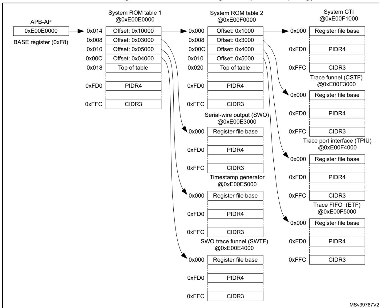
The diagram illustrates the APB-D CoreSight component topology. It shows the following components and their connections:
- APB-AP : Base register at 0xE00E0000 (0xF8). It points to the start of System ROM table 1 at 0x014.
- System ROM table 1 @0xE00E0000
: Contains entries for various components with their address offsets:
- 0x014: Offset: 0x10000 (points to System ROM table 2)
- 0x008: Offset: 0x03000 (points to SWO)
- 0x010: Offset: 0x05000 (points to Timestamp generator)
- 0x00C: Offset: 0x04000 (points to SWTF)
- 0x018: Top of table
- 0xFD0: PIDR4
- 0xFFC: CIDR3
- System ROM table 2 @0xE00F0000
: Contains entries for:
- 0x000: Offset: 0x1000 (points to System CTI)
- 0x008: Offset: 0x03000 (points to Trace funnel (CSTF))
- 0x00C: Offset: 0x04000 (points to Trace port interface (TPIU))
- 0x010: Offset: 0x05000 (points to Trace FIFO (ETF))
- 0x020: Top of table
- 0xFD0: PIDR4
- 0xFFC: CIDR3
- System CTI @0xE00F1000
: Contains:
- 0x000: Register file base
- 0xFD0: PIDR4
- 0xFFC: CIDR3
- Trace funnel (CSTF) @0xE00F3000
: Contains:
- 0x000: Register file base
- 0xFD0: PIDR4
- 0xFFC: CIDR3
- Trace port interface (TPIU) @0xE00F4000
: Contains:
- 0x000: Register file base
- 0xFD0: PIDR4
- 0xFFC: CIDR3
- Trace FIFO (ETF) @0xE00F5000
: Contains:
- 0x000: Register file base
- 0xFD0: PIDR4
- 0xFFC: CIDR3
- Serial-wire output (SWO) @0xE00E3000
: Contains:
- 0x000: Register file base
- 0xFD0: PIDR4
- 0xFFC: CIDR3
- Timestamp generator @0xE00E5000
: Contains:
- 0x000: Register file base
- 0xFD0: PIDR4
- 0xFFC: CIDR3
- SWO trace funnel (SWTF) @0xE00E4000
: Contains:
- 0x000: Register file base
- 0xFD0: PIDR4
- 0xFFC: CIDR3
MSV39787V2
For more information on the use of the ROM table, refer to the Arm® Debug Interface Architecture Specification [1].
System ROM registers
SYSROM memory type register (SYSROM_MEMTYPE)
Address offset: 0xFCC
Reset value: 0x0000 0000
| 31 | 30 | 29 | 28 | 27 | 26 | 25 | 24 | 23 | 22 | 21 | 20 | 19 | 18 | 17 | 16 |
|---|---|---|---|---|---|---|---|---|---|---|---|---|---|---|---|
| Res. | Res. | Res. | Res. | Res. | Res. | Res. | Res. | Res. | Res. | Res. | Res. | Res. | Res. | Res. | Res. |
| 15 | 14 | 13 | 12 | 11 | 10 | 9 | 8 | 7 | 6 | 5 | 4 | 3 | 2 | 1 | 0 |
| Res. | Res. | Res. | Res. | Res. | Res. | Res. | Res. | Res. | Res. | Res. | Res. | Res. | Res. | Res. | SYSEM |
| r |
Bits 31:1 Reserved, must be kept at reset value.
Bit 0 SYSEM : System memory
0: No system memory is present on this bus
SYSROM CoreSight peripheral identity register 4 (SYSROM_PIDR4)
Address offset: 0xFD0
Reset value: 0x0000 0000
| 31 | 30 | 29 | 28 | 27 | 26 | 25 | 24 | 23 | 22 | 21 | 20 | 19 | 18 | 17 | 16 |
|---|---|---|---|---|---|---|---|---|---|---|---|---|---|---|---|
| Res. | Res. | Res. | Res. | Res. | Res. | Res. | Res. | Res. | Res. | Res. | Res. | Res. | Res. | Res. | Res. |
| 15 | 14 | 13 | 12 | 11 | 10 | 9 | 8 | 7 | 6 | 5 | 4 | 3 | 2 | 1 | 0 |
| Res. | Res. | Res. | Res. | Res. | Res. | Res. | Res. | 4KCOUNT[3:0] | JEP106CON[3:0] | ||||||
| r | r | r | r | r | r | r | r | ||||||||
Bits 31:8 Reserved, must be kept at reset value.
Bits 7:4 4KCOUNT[3:0] : Register file size
0x0: Register file occupies a single 4 Kbyte region
Bits 3:0 JEP106CON[3:0] : JEP106 continuation code
0x0: STMicroelectronics JEDEC continuation code
SYSROM CoreSight peripheral identity register 0 (SYSROM_PIDR0)
Address offset: 0xFE0
Reset value: 0x0000 0050 (System ROM table 1), 0x0000 0001 (System ROM table 2)
| 31 | 30 | 29 | 28 | 27 | 26 | 25 | 24 | 23 | 22 | 21 | 20 | 19 | 18 | 17 | 16 |
|---|---|---|---|---|---|---|---|---|---|---|---|---|---|---|---|
| Res. | Res. | Res. | Res. | Res. | Res. | Res. | Res. | Res. | Res. | Res. | Res. | Res. | Res. | Res. | Res. |
| 15 | 14 | 13 | 12 | 11 | 10 | 9 | 8 | 7 | 6 | 5 | 4 | 3 | 2 | 1 | 0 |
| Res. | Res. | Res. | Res. | Res. | Res. | Res. | Res. | PARTNUM[7:0] | |||||||
| r | r | r | r | r | r | r | r | ||||||||
Bits 31:8 Reserved, must be kept at reset value.
Bits 7:0 PARTNUM[7:0] : Device part number field, bits [7:0]
- 0x50: STM32H7 device (System ROM table 1)
- 0x01: STM32H7 device (System ROM table 2)
SYSROM CoreSight peripheral identity register 1 (SYSROM_PIDR1)
Address offset: 0xFE4
Reset value: 0x0000 0004 (System ROM table 1), 0x0000 0000 (System ROM table 2)
| 31 | 30 | 29 | 28 | 27 | 26 | 25 | 24 | 23 | 22 | 21 | 20 | 19 | 18 | 17 | 16 |
|---|---|---|---|---|---|---|---|---|---|---|---|---|---|---|---|
| Res. | Res. | Res. | Res. | Res. | Res. | Res. | Res. | Res. | Res. | Res. | Res. | Res. | Res. | Res. | Res. |
| 15 | 14 | 13 | 12 | 11 | 10 | 9 | 8 | 7 | 6 | 5 | 4 | 3 | 2 | 1 | 0 |
| Res. | Res. | Res. | Res. | Res. | Res. | Res. | Res. | JEP106ID[3:0] | PARTNUM[11:8] | ||||||
| r | r | r | r | r | r | r | r | ||||||||
Bits 31:8 Reserved, must be kept at reset value.
Bits 7:4 JEP106ID[3:0] : JEP106 identity code field, bits [3:0]
- 0x0: STMicroelectronics JEDEC code
Bits 3:0 PARTNUM[11:8] : Device part number field, bits [11:8]
- 0x4: STM32H7 device System ROM table 1
- 0x0: STM32H7 device System ROM table 2
SYSROM CoreSight peripheral identity register 2 (SYSROM_PIDR2)
Address offset: 0xFE8
Reset value: 0x0000 000A
| 31 | 30 | 29 | 28 | 27 | 26 | 25 | 24 | 23 | 22 | 21 | 20 | 19 | 18 | 17 | 16 |
|---|---|---|---|---|---|---|---|---|---|---|---|---|---|---|---|
| Res. | Res. | Res. | Res. | Res. | Res. | Res. | Res. | Res. | Res. | Res. | Res. | Res. | Res. | Res. | Res. |
| 15 | 14 | 13 | 12 | 11 | 10 | 9 | 8 | 7 | 6 | 5 | 4 | 3 | 2 | 1 | 0 |
|---|---|---|---|---|---|---|---|---|---|---|---|---|---|---|---|
| Res. | Res. | Res. | Res. | Res. | Res. | Res. | Res. | REVISION[3:0] | JEDEC | JEP106ID[6:4] | |||||
| r | r | r | r | r | r | r | r | ||||||||
Bits 31:8 Reserved, must be kept at reset value.
Bits 7:4 REVISION[3:0] : Device revision number
0x0: Rev 0
Bit 3 JEDEC : JEDEC assigned value
1: Designer ID specified by JEDEC
Bits 2:0 JEP106ID[6:4] : JEP106 identity code field, bits [6:4]
0x2: STMicroelectronics JEDEC code
SYSROM CoreSight peripheral identity register 3 (SYSROM_PIDR3)
Address offset: 0xFEC
Reset value: 0x0000 0000
| 31 | 30 | 29 | 28 | 27 | 26 | 25 | 24 | 23 | 22 | 21 | 20 | 19 | 18 | 17 | 16 |
|---|---|---|---|---|---|---|---|---|---|---|---|---|---|---|---|
| Res. | Res. | Res. | Res. | Res. | Res. | Res. | Res. | Res. | Res. | Res. | Res. | Res. | Res. | Res. | Res. |
| 15 | 14 | 13 | 12 | 11 | 10 | 9 | 8 | 7 | 6 | 5 | 4 | 3 | 2 | 1 | 0 |
| Res. | Res. | Res. | Res. | Res. | Res. | Res. | Res. | REVAND[3:0] | CMOD[3:0] | ||||||
| r | r | r | r | r | r | r | r | ||||||||
Bits 31:8 Reserved, must be kept at reset value.
Bits 7:4 REVAND[3:0] : Metal fix version
0x0: No metal fix
Bits 3:0 CMOD[3:0] : Customer modified
0x0: No customer modifications
SYSROM CoreSight component identity register 0 (SYSROM_CIDR0)
Address offset: 0xFF0
Reset value: 0x0000 000D
| 31 | 30 | 29 | 28 | 27 | 26 | 25 | 24 | 23 | 22 | 21 | 20 | 19 | 18 | 17 | 16 |
|---|---|---|---|---|---|---|---|---|---|---|---|---|---|---|---|
| Res. | Res. | Res. | Res. | Res. | Res. | Res. | Res. | Res. | Res. | Res. | Res. | Res. | Res. | Res. | Res. |
| 15 | 14 | 13 | 12 | 11 | 10 | 9 | 8 | 7 | 6 | 5 | 4 | 3 | 2 | 1 | 0 |
| Res. | Res. | Res. | Res. | Res. | Res. | Res. | Res. | PREAMBLE[7:0] | |||||||
| r | r | r | r | r | r | r | r | ||||||||
Bits 31:8 Reserved, must be kept at reset value.
Bits 7:0
PREAMBLE[7:0]
: Component ID field, bits [7:0]
0x0D: Common ID value
SYSROM CoreSight component identity register 1 (SYSROM_CIDR1)
Address offset: 0xFF4
Reset value: 0x0000 0010
| 31 | 30 | 29 | 28 | 27 | 26 | 25 | 24 | 23 | 22 | 21 | 20 | 19 | 18 | 17 | 16 |
|---|---|---|---|---|---|---|---|---|---|---|---|---|---|---|---|
| Res. | Res. | Res. | Res. | Res. | Res. | Res. | Res. | Res. | Res. | Res. | Res. | Res. | Res. | Res. | Res. |
| 15 | 14 | 13 | 12 | 11 | 10 | 9 | 8 | 7 | 6 | 5 | 4 | 3 | 2 | 1 | 0 |
| Res. | Res. | Res. | Res. | Res. | Res. | Res. | Res. | CLASS[3:0] | PREAMBLE[11:8] | ||||||
| r | r | r | r | r | r | r | r | ||||||||
Bits 31:8 Reserved, must be kept at reset value.
Bits 7:4
CLASS[3:0]
: Component ID field, bits [15:12] - component class
0x1: ROM table component
Bits 3:0
PREAMBLE[11:8]
: Component ID field, bits [11:8]
0x0: Common ID value
SYSROM CoreSight component identity register 2 (SYSROM_CIDR2)
Address offset: 0xFF8
Reset value: 0x0000 0005
| 31 | 30 | 29 | 28 | 27 | 26 | 25 | 24 | 23 | 22 | 21 | 20 | 19 | 18 | 17 | 16 |
|---|---|---|---|---|---|---|---|---|---|---|---|---|---|---|---|
| Res. | Res. | Res. | Res. | Res. | Res. | Res. | Res. | Res. | Res. | Res. | Res. | Res. | Res. | Res. | Res. |
| 15 | 14 | 13 | 12 | 11 | 10 | 9 | 8 | 7 | 6 | 5 | 4 | 3 | 2 | 1 | 0 |
| Res. | Res. | Res. | Res. | Res. | Res. | Res. | Res. | PREAMBLE[19:12] | |||||||
| r | r | r | r | r | r | r | r | ||||||||
Bits 31:8 Reserved, must be kept at reset value.
Bits 7:0
PREAMBLE[19:12]
: Component ID field, bits [23:16]
0x05: Common ID value
SYSROM CoreSight component identity register 3 (SYSROM_CIDR3)
Address offset: 0xFFC
Reset value: 0x0000 00B1
| 31 | 30 | 29 | 28 | 27 | 26 | 25 | 24 | 23 | 22 | 21 | 20 | 19 | 18 | 17 | 16 |
|---|---|---|---|---|---|---|---|---|---|---|---|---|---|---|---|
| Res. | Res. | Res. | Res. | Res. | Res. | Res. | Res. | Res. | Res. | Res. | Res. | Res. | Res. | Res. | Res. |
| 15 | 14 | 13 | 12 | 11 | 10 | 9 | 8 | 7 | 6 | 5 | 4 | 3 | 2 | 1 | 0 |
| Res. | Res. | Res. | Res. | Res. | Res. | Res. | Res. | PREAMBLE[27:20] | |||||||
| r | r | r | r | r | r | r | r | ||||||||
Bits 31:8 Reserved, must be kept at reset value.
Bits 7:0 PREAMBLE[27:20] : Component ID field, bits [31:24]
0xB1: Common ID value
System ROM register map and reset values
Table 627. System ROM table 1 register map and reset values
| Offset | Register name | 31 | 30 | 29 | 28 | 27 | 26 | 25 | 24 | 23 | 22 | 21 | 20 | 19 | 18 | 17 | 16 | 15 | 14 | 13 | 12 | 11 | 10 | 9 | 8 | 7 | 6 | 5 | 4 | 3 | 2 | 1 | 0 |
|---|---|---|---|---|---|---|---|---|---|---|---|---|---|---|---|---|---|---|---|---|---|---|---|---|---|---|---|---|---|---|---|---|---|
| 0xFFC | SYSROM_MEMTYPE | Res. | Res. | Res. | Res. | Res. | Res. | Res. | Res. | Res. | Res. | Res. | Res. | Res. | Res. | Res. | Res. | Res. | Res. | Res. | Res. | Res. | Res. | Res. | Res. | Res. | Res. | Res. | Res. | Res. | Res. | Res. | SYSMEM |
| Reset value | 0 | ||||||||||||||||||||||||||||||||
| 0xFD0 | SYSROM_PIDR4 | Res. | Res. | Res. | Res. | Res. | Res. | Res. | Res. | Res. | Res. | Res. | Res. | Res. | Res. | Res. | Res. | Res. | Res. | Res. | Res. | Res. | Res. | Res. | Res. | Res. | 4KCOUNT[3:0] | JEP106CON[3:0] | |||||
| Reset value | 0 | 0 | 0 | 0 | 0 | 0 | 0 | ||||||||||||||||||||||||||
| 0xFD4 to 0xFDC | Reserved | Reserved | |||||||||||||||||||||||||||||||
| 0xFE0 | SYSROM_PIDR0 | Res. | Res. | Res. | Res. | Res. | Res. | Res. | Res. | Res. | Res. | Res. | Res. | Res. | Res. | Res. | Res. | Res. | Res. | Res. | Res. | Res. | Res. | Res. | Res. | Res. | PARTNUM[7:0] | ||||||
| Reset value | 0 | 1 | 0 | 1 | 0 | 0 | 0 | ||||||||||||||||||||||||||
| 0xFE4 | SYSROM_PIDR1 | Res. | Res. | Res. | Res. | Res. | Res. | Res. | Res. | Res. | Res. | Res. | Res. | Res. | Res. | Res. | Res. | Res. | Res. | Res. | Res. | Res. | Res. | Res. | Res. | JEP106ID[3:0] | PARTNUM[11:8] | ||||||
| Reset value | 0 | 0 | 0 | 0 | 0 | 1 | 0 | 0 | |||||||||||||||||||||||||
| 0xFE8 | SYSROM_PIDR2 | Res. | Res. | Res. | Res. | Res. | Res. | Res. | Res. | Res. | Res. | Res. | Res. | Res. | Res. | Res. | Res. | Res. | Res. | Res. | Res. | Res. | Res. | Res. | Res. | REVISION[3:0] | JEDEC | JEP106ID[6:4] | |||||
| Reset value | 0 | 0 | 0 | 0 | 1 | 0 | 1 | 0 | |||||||||||||||||||||||||
Table 627. System ROM table 1 register map and reset values (continued)
| Offset | Register name | 31 | 30 | 29 | 28 | 27 | 26 | 25 | 24 | 23 | 22 | 21 | 20 | 19 | 18 | 17 | 16 | 15 | 14 | 13 | 12 | 11 | 10 | 9 | 8 | 7 | 6 | 5 | 4 | 3 | 2 | 1 | 0 |
|---|---|---|---|---|---|---|---|---|---|---|---|---|---|---|---|---|---|---|---|---|---|---|---|---|---|---|---|---|---|---|---|---|---|
| 0xFEC | SYSROM_PIDR3 | Res. | Res. | Res. | Res. | Res. | Res. | Res. | Res. | Res. | Res. | Res. | Res. | Res. | Res. | Res. | Res. | Res. | Res. | Res. | Res. | Res. | Res. | Res. | Res. | REVAND[3:0] | CMOD[3:0] | ||||||
| Reset value | 0 | 0 | 0 | 0 | 0 | 0 | 0 | 0 | |||||||||||||||||||||||||
| 0xFF0 | SYSROM_CIDR0 | Res. | Res. | Res. | Res. | Res. | Res. | Res. | Res. | Res. | Res. | Res. | Res. | Res. | Res. | Res. | Res. | Res. | Res. | Res. | Res. | Res. | Res. | Res. | PREAMBLE[7:0] | ||||||||
| Reset value | 0 | 0 | 0 | 0 | 1 | 1 | 0 | 1 | |||||||||||||||||||||||||
| 0xFF4 | SYSROM_CIDR1 | Res. | Res. | Res. | Res. | Res. | Res. | Res. | Res. | Res. | Res. | Res. | Res. | Res. | Res. | Res. | Res. | Res. | Res. | Res. | Res. | Res. | Res. | Res. | CLASS[3:0] | PREAMBLE[11:8] | |||||||
| Reset value | 0 | 0 | 0 | 1 | 0 | 0 | 0 | 0 | |||||||||||||||||||||||||
| 0xFF8 | SYSROM_CIDR2 | Res. | Res. | Res. | Res. | Res. | Res. | Res. | Res. | Res. | Res. | Res. | Res. | Res. | Res. | Res. | Res. | Res. | Res. | Res. | Res. | Res. | Res. | Res. | PREAMBLE[19:12] | ||||||||
| Reset value | 0 | 0 | 0 | 0 | 0 | 1 | 0 | 1 | |||||||||||||||||||||||||
| 0xFFC | SYSROM_CIDR3 | Res. | Res. | Res. | Res. | Res. | Res. | Res. | Res. | Res. | Res. | Res. | Res. | Res. | Res. | Res. | Res. | Res. | Res. | Res. | Res. | Res. | Res. | Res. | PREAMBLE[27:20] | ||||||||
| Reset value | 1 | 0 | 1 | 1 | 0 | 0 | 0 | 1 | |||||||||||||||||||||||||
Table 628. System ROM table 2 register map and reset values
| Offset | Register name | 31 | 30 | 29 | 28 | 27 | 26 | 25 | 24 | 23 | 22 | 21 | 20 | 19 | 18 | 17 | 16 | 15 | 14 | 13 | 12 | 11 | 10 | 9 | 8 | 7 | 6 | 5 | 4 | 3 | 2 | 1 | 0 |
|---|---|---|---|---|---|---|---|---|---|---|---|---|---|---|---|---|---|---|---|---|---|---|---|---|---|---|---|---|---|---|---|---|---|
| 0xFCC | SYSROM_MEMTYPE | Res. | Res. | Res. | Res. | Res. | Res. | Res. | Res. | Res. | Res. | Res. | Res. | Res. | Res. | Res. | Res. | Res. | Res. | Res. | Res. | Res. | Res. | Res. | Res. | Res. | Res. | Res. | Res. | Res. | Res. | Res. | 0 |
| Reset value | 0 | ||||||||||||||||||||||||||||||||
| 0xFD0 | SYSROM_PIDR4 | Res. | Res. | Res. | Res. | Res. | Res. | Res. | Res. | Res. | Res. | Res. | Res. | Res. | Res. | Res. | Res. | Res. | Res. | Res. | Res. | Res. | Res. | Res. | 4KCOUNT[3:0] | JEP106CON[3:0] | |||||||
| Reset value | 0 | 0 | 0 | 0 | 0 | 0 | 0 | 0 | |||||||||||||||||||||||||
| 0xFD4 to 0xFDC | Reserved | Reserved | |||||||||||||||||||||||||||||||
| 0xFE0 | SYSROM_PIDR0 | Res. | Res. | Res. | Res. | Res. | Res. | Res. | Res. | Res. | Res. | Res. | Res. | Res. | Res. | Res. | Res. | Res. | Res. | Res. | Res. | Res. | Res. | Res. | PARTNUM[7:0] | ||||||||
| Reset value | 0 | 0 | 0 | 0 | 0 | 0 | 0 | 1 | |||||||||||||||||||||||||
| 0xFE4 | SYSROM_PIDR1 | Res. | Res. | Res. | Res. | Res. | Res. | Res. | Res. | Res. | Res. | Res. | Res. | Res. | Res. | Res. | Res. | Res. | Res. | Res. | Res. | Res. | Res. | Res. | JEP106ID[3:0] | PARTNUM[11:8] | |||||||
| Reset value | 0 | 0 | 0 | 0 | 0 | 0 | 0 | 0 | |||||||||||||||||||||||||
Table 628. System ROM table 2 register map and reset values (continued)
| Offset | Register name | 31 | 30 | 29 | 28 | 27 | 26 | 25 | 24 | 23 | 22 | 21 | 20 | 19 | 18 | 17 | 16 | 15 | 14 | 13 | 12 | 11 | 10 | 9 | 8 | 7 | 6 | 5 | 4 | 3 | 2 | 1 | 0 | |
|---|---|---|---|---|---|---|---|---|---|---|---|---|---|---|---|---|---|---|---|---|---|---|---|---|---|---|---|---|---|---|---|---|---|---|
| 0xFE8 | SYSROM_PIDR2 | Res. | Res. | Res. | Res. | Res. | Res. | Res. | Res. | Res. | Res. | Res. | Res. | Res. | Res. | Res. | Res. | Res. | Res. | Res. | Res. | Res. | Res. | Res. | Res. | Res. | REVISION[3:0] | JEDEC | JEP106ID[6:4] | |||||
| Reset value | 0 | 0 | 0 | 0 | 1 | 0 | 1 | 0 | ||||||||||||||||||||||||||
| 0xFEC | SYSROM_PIDR3 | Res. | Res. | Res. | Res. | Res. | Res. | Res. | Res. | Res. | Res. | Res. | Res. | Res. | Res. | Res. | Res. | Res. | Res. | Res. | Res. | Res. | Res. | Res. | Res. | Res. | REVAND[3:0] | CMOD[3:0] | ||||||
| Reset value | 0 | 0 | 0 | 0 | 0 | 0 | 0 | 0 | ||||||||||||||||||||||||||
| 0xFF0 | SYSROM_CIDR0 | Res. | Res. | Res. | Res. | Res. | Res. | Res. | Res. | Res. | Res. | Res. | Res. | Res. | Res. | Res. | Res. | Res. | Res. | Res. | Res. | Res. | Res. | Res. | Res. | PREAMBLE[7:0] | ||||||||
| Reset value | 0 | 0 | 0 | 0 | 1 | 1 | 0 | 1 | ||||||||||||||||||||||||||
| 0xFF4 | SYSROM_CIDR1 | Res. | Res. | Res. | Res. | Res. | Res. | Res. | Res. | Res. | Res. | Res. | Res. | Res. | Res. | Res. | Res. | Res. | Res. | Res. | Res. | Res. | Res. | Res. | Res. | CLASS[3:0] | PREAMBLE[11:8] | |||||||
| Reset value | 0 | 0 | 0 | 1 | 0 | 0 | 0 | 0 | ||||||||||||||||||||||||||
| 0xFF8 | SYSROM_CIDR2 | Res. | Res. | Res. | Res. | Res. | Res. | Res. | Res. | Res. | Res. | Res. | Res. | Res. | Res. | Res. | Res. | Res. | Res. | Res. | Res. | Res. | Res. | Res. | Res. | PREAMBLE[19:12] | ||||||||
| Reset value | 0 | 0 | 0 | 0 | 0 | 1 | 0 | 1 | ||||||||||||||||||||||||||
| 0xFFC | SYSROM_CIDR3 | Res. | Res. | Res. | Res. | Res. | Res. | Res. | Res. | Res. | Res. | Res. | Res. | Res. | Res. | Res. | Res. | Res. | Res. | Res. | Res. | Res. | Res. | Res. | Res. | PREAMBLE[27:20] | ||||||||
| Reset value | 1 | 0 | 1 | 1 | 0 | 0 | 0 | 1 |
63.5.2 Global timestamp generator (TSG)
The global timestamp generator contains a 64-bit counter that provides a common timing reference for all of the trace sources in the system, namely the ETM and ITM in each processor core. These components insert timestamps in the trace streams that allow the trace analyzer to recover the chronological order of trace packets, which can be lost when multiple trace sources are multiplexed into one stream at the funnels.
The TSG registers are accessible over the APB-D. This allows the debugger or debug software to:
- • start and stop the timestamp incrementing
- • read the current timestamp value
- • change the current timestamp value
- – The timestamp counter must be halted while it is changed. When the timestamp value is changed, the timestamp generator resynchronizes all the trace sources.
- • change the reported timestamp increment
For more information on the global timestamp generator CoreSight component, refer to the Arm® CoreSight™ SoC-400 Technical Reference Manual [2].
The timestamp generator is located in the D3 power domain, and the timestamp is distributed to the Cortex-M7 and Cortex-M4. To simplify the distribution over power domain
boundaries, the 64-bit timestamp is encoded in seven bits, then decoded in the destination power domain, and interpolated to increase its resolution if the processor clock is significantly faster than the generator clock. The timestamp distribution is shown in Figure 877.
Figure 877. Global timestamp distribution
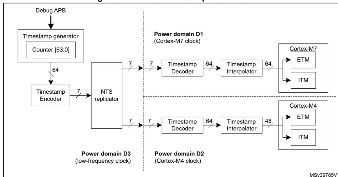
The diagram illustrates the global timestamp distribution. A Debug APB interface connects to a Timestamp generator containing a Counter [63:0]. The 64-bit counter output is passed to a Timestamp Encoder, which outputs a 7-bit signal. This signal is then replicated by an NTS replicator. The replicated 7-bit signals are distributed to two power domains: Power domain D1 (Cortex-M7 clock) and Power domain D2 (Cortex-M4 clock). In each domain, the 7-bit signal is decoded by a Timestamp Decoder back into a 64-bit signal. This 64-bit signal is then processed by a Timestamp Interpolator. The output of the interpolator in Power domain D1 is sent to a Cortex-M7 processor's ETM and ITM units. The output of the interpolator in Power domain D2 is sent to a Cortex-M4 processor's ETM and ITM units. Power domain D3 (low-frequency clock) is also shown, but its connection to the timestamp distribution is not fully detailed in this view. The diagram is labeled MSv39785V1.
TSG registers
TSG counter control register (TSG_CNTCR)
Address offset: 0x000
Reset value: 0x0000 0000
| 31 | 30 | 29 | 28 | 27 | 26 | 25 | 24 | 23 | 22 | 21 | 20 | 19 | 18 | 17 | 16 |
|---|---|---|---|---|---|---|---|---|---|---|---|---|---|---|---|
| Res. | Res. | Res. | Res. | Res. | Res. | Res. | Res. | Res. | Res. | Res. | Res. | Res. | Res. | Res. | Res. |
| 15 | 14 | 13 | 12 | 11 | 10 | 9 | 8 | 7 | 6 | 5 | 4 | 3 | 2 | 1 | 0 |
| Res. | Res. | Res. | Res. | Res. | Res. | Res. | Res. | Res. | Res. | Res. | Res. | Res. | Res. | HDBG | EN |
| rw | rw |
Bits 31:2 Reserved, must be kept at reset value.
Bit 1 HDBG : Halt on debug
0: Normal operation
1: Halt counter when system-wide debug state is detected - not implemented
Bit 0 EN : Enable
0: Counter disabled
1: Counter enabled and incrementing
TSG counter status register (TSG_CNTSR)
Address offset: 0x004
Reset value: 0x0000 0000
| 31 | 30 | 29 | 28 | 27 | 26 | 25 | 24 | 23 | 22 | 21 | 20 | 19 | 18 | 17 | 16 |
|---|---|---|---|---|---|---|---|---|---|---|---|---|---|---|---|
| Res. | Res. | Res. | Res. | Res. | Res. | Res. | Res. | Res. | Res. | Res. | Res. | Res. | Res. | Res. | Res. |
| 15 | 14 | 13 | 12 | 11 | 10 | 9 | 8 | 7 | 6 | 5 | 4 | 3 | 2 | 1 | 0 |
| Res. | Res. | Res. | Res. | Res. | Res. | Res. | Res. | Res. | Res. | Res. | Res. | Res. | Res. | DBGH | Res. |
| r |
Bits 31:2 Reserved, must be kept at reset value.
Bit 1 DBGH : Debug halt
0: Normal operation
1: Counter halted due to system-wide debug state
Bit 0 Reserved, must be kept at reset value.
TSG current counter value lower register (TSG_CNTCVL)
Address offset: 0x008
Reset value: 0x0000 0000
| 31 | 30 | 29 | 28 | 27 | 26 | 25 | 24 | 23 | 22 | 21 | 20 | 19 | 18 | 17 | 16 |
|---|---|---|---|---|---|---|---|---|---|---|---|---|---|---|---|
| CNTCVL[31:16] | |||||||||||||||
| rw | rw | rw | rw | rw | rw | rw | rw | rw | rw | rw | rw | rw | rw | rw | rw |
| 15 | 14 | 13 | 12 | 11 | 10 | 9 | 8 | 7 | 6 | 5 | 4 | 3 | 2 | 1 | 0 |
| CNTCVL[15:0] | |||||||||||||||
| rw | rw | rw | rw | rw | rw | rw | rw | rw | rw | rw | rw | rw | rw | rw | rw |
Bits 31:0 CNTCVL[31:0] : TSG current counter value field, bits[31:0]
To change the current timestamp value, write the lower 32 bits of the new value to this register before writing the upper 32 bits to CNTCVU. The timestamp value is not changed until the CNTCVU register is written to. Note: The TSG_CNTCR register's EN bit must be cleared before writing to this register.
TSG current counter value upper register (TSG_CNTCVU)
Address offset: 0x00C
Reset value: 0x0000 0000
| 31 | 30 | 29 | 28 | 27 | 26 | 25 | 24 | 23 | 22 | 21 | 20 | 19 | 18 | 17 | 16 |
|---|---|---|---|---|---|---|---|---|---|---|---|---|---|---|---|
| CNTCVU[31:16] | |||||||||||||||
| rw | rw | rw | rw | rw | rw | rw | rw | rw | rw | rw | rw | rw | rw | rw | rw |
| 15 | 14 | 13 | 12 | 11 | 10 | 9 | 8 | 7 | 6 | 5 | 4 | 3 | 2 | 1 | 0 |
| CNTCVU[15:0] | |||||||||||||||
| rw | rw | rw | rw | rw | rw | rw | rw | rw | rw | rw | rw | rw | rw | rw | rw |
Bits 31:0 CNTCVU[31:0] : TSG current counter value field, bits[63:32]
To change the current timestamp value, write the lower 32 bits of the new value to CNTCVL before writing the upper 32 bits to this register. The 64-bit timestamp value is updated with the value from both writes when this register is written to. Note: The TSG_CNTCR register's EN bit must be cleared before writing to this register.
TSG base frequency ID register (TSG_CNTFID0)
Address offset: 0x020
Reset value: 0x0000 0000
| 31 | 30 | 29 | 28 | 27 | 26 | 25 | 24 | 23 | 22 | 21 | 20 | 19 | 18 | 17 | 16 |
| FREQ[31:16] | |||||||||||||||
| rw | rw | rw | rw | rw | rw | rw | rw | rw | rw | rw | rw | rw | rw | rw | rw |
| 15 | 14 | 13 | 12 | 11 | 10 | 9 | 8 | 7 | 6 | 5 | 4 | 3 | 2 | 1 | 0 |
| FREQ[15:0] | |||||||||||||||
| rw | rw | rw | rw | rw | rw | rw | rw | rw | rw | rw | rw | rw | rw | rw | rw |
Bits 31:0 FREQ[31:0] : Increment frequency of TSG counter in Hz
This field must be programmed with the trace generator clock frequency whenever it changes.
TSG CoreSight peripheral identity register 4 (TSG_PIDR4)
Address offset: 0xFD0
Reset value: 0x0000 0004
| 31 | 30 | 29 | 28 | 27 | 26 | 25 | 24 | 23 | 22 | 21 | 20 | 19 | 18 | 17 | 16 |
| Res. | Res. | Res. | Res. | Res. | Res. | Res. | Res. | Res. | Res. | Res. | Res. | Res. | Res. | Res. | Res. |
| 15 | 14 | 13 | 12 | 11 | 10 | 9 | 8 | 7 | 6 | 5 | 4 | 3 | 2 | 1 | 0 |
| Res. | Res. | Res. | Res. | Res. | Res. | Res. | Res. | 4KCOUNT[3:0] | JEP106CON[3:0] | ||||||
| r | r | r | r | r | r | r | r | ||||||||
Bits 31:8 Reserved, must be kept at reset value.
Bits 7:4 4KCOUNT[3:0] : Register file size
0x0: Register file occupies a single 4 Kbyte region
Bits 3:0 JEP106CON[3:0] : JEP106 continuation code
0x4: Arm® JEDEC code
TSG CoreSight Peripheral identity register 0 (TSG_PIDR0)
Address offset: 0xFE0
Reset value: 0x0000 0001
| 31 | 30 | 29 | 28 | 27 | 26 | 25 | 24 | 23 | 22 | 21 | 20 | 19 | 18 | 17 | 16 |
|---|---|---|---|---|---|---|---|---|---|---|---|---|---|---|---|
| Res. | Res. | Res. | Res. | Res. | Res. | Res. | Res. | Res. | Res. | Res. | Res. | Res. | Res. | Res. | Res. |
| 15 | 14 | 13 | 12 | 11 | 10 | 9 | 8 | 7 | 6 | 5 | 4 | 3 | 2 | 1 | 0 |
| Res. | Res. | Res. | Res. | Res. | Res. | Res. | Res. | PARTNUM[7:0] | |||||||
| r | r | r | r | r | r | r | r | ||||||||
Bits 31:8 Reserved, must be kept at reset value.
Bits 7:0 PARTNUM[7:0] : Part number field, bits [7:0]
0x01: TSG part number
TSG CoreSight peripheral identity register 1 (TSG_PIDR1)
Address offset: 0xFE4
Reset value: 0x0000 00B1
| 31 | 30 | 29 | 28 | 27 | 26 | 25 | 24 | 23 | 22 | 21 | 20 | 19 | 18 | 17 | 16 |
|---|---|---|---|---|---|---|---|---|---|---|---|---|---|---|---|
| Res. | Res. | Res. | Res. | Res. | Res. | Res. | Res. | Res. | Res. | Res. | Res. | Res. | Res. | Res. | Res. |
| 15 | 14 | 13 | 12 | 11 | 10 | 9 | 8 | 7 | 6 | 5 | 4 | 3 | 2 | 1 | 0 |
| Res. | Res. | Res. | Res. | Res. | Res. | Res. | Res. | JEP106ID[3:0] | PARTNUM[11:8] | ||||||
| r | r | r | r | r | r | r | r | ||||||||
Bits 31:8 Reserved, must be kept at reset value.
Bits 7:4 JEP106ID[3:0] : JEP106 identity code field, bits [3:0]
0xB: Arm ® JEDEC code
Bits 3:0 PARTNUM[11:8] : Part number field, bits [11:8]
0x1: TSG part number
TSG CoreSight peripheral identity register 2 (TSG_PIDR2)
Address offset: 0xFE8
Reset value: 0x0000 001B
| 31 | 30 | 29 | 28 | 27 | 26 | 25 | 24 | 23 | 22 | 21 | 20 | 19 | 18 | 17 | 16 |
|---|---|---|---|---|---|---|---|---|---|---|---|---|---|---|---|
| Res. | Res. | Res. | Res. | Res. | Res. | Res. | Res. | Res. | Res. | Res. | Res. | Res. | Res. | Res. | Res. |
| 15 | 14 | 13 | 12 | 11 | 10 | 9 | 8 | 7 | 6 | 5 | 4 | 3 | 2 | 1 | 0 |
|---|---|---|---|---|---|---|---|---|---|---|---|---|---|---|---|
| Res. | Res. | Res. | Res. | Res. | Res. | Res. | Res. | REVISION[3:0] | JEDEC | JEP106ID[6:4] | |||||
| r | r | r | r | r | r | r | r | ||||||||
Bits 31:8 Reserved, must be kept at reset value.
Bits 7:4 REVISION[3:0] : Component revision number
0x1: r0p1
Bit 3 JEDEC : JEDEC assigned value
1: Designer ID specified by JEDEC
Bits 2:0 JEP106ID[6:4] : JEP106 identity code field, bits [6:4]
0x3: Arm® JEDEC code
TSG CoreSight peripheral identity register 3 (TSG_PIDR3)
Address offset: 0xFEC
Reset value: 0x0000 0000
| 31 | 30 | 29 | 28 | 27 | 26 | 25 | 24 | 23 | 22 | 21 | 20 | 19 | 18 | 17 | 16 |
|---|---|---|---|---|---|---|---|---|---|---|---|---|---|---|---|
| Res. | Res. | Res. | Res. | Res. | Res. | Res. | Res. | Res. | Res. | Res. | Res. | Res. | Res. | Res. | Res. |
| 15 | 14 | 13 | 12 | 11 | 10 | 9 | 8 | 7 | 6 | 5 | 4 | 3 | 2 | 1 | 0 |
| Res. | Res. | Res. | Res. | Res. | Res. | Res. | Res. | REVAND[3:0] | CMOD[3:0] | ||||||
| r | r | r | r | r | r | r | r | ||||||||
Bits 31:8 Reserved, must be kept at reset value.
Bits 7:4 REVAND[3:0] : Metal fix version
0x0: No metal fix
Bits 3:0 CMOD[3:0] : Customer modified
0x0: No customer modifications
TSG CoreSight component identity register 0 (TSG_CIDR0)
Address offset: 0xFF0
Reset value: 0x0000 000D
| 31 | 30 | 29 | 28 | 27 | 26 | 25 | 24 | 23 | 22 | 21 | 20 | 19 | 18 | 17 | 16 |
|---|---|---|---|---|---|---|---|---|---|---|---|---|---|---|---|
| Res. | Res. | Res. | Res. | Res. | Res. | Res. | Res. | Res. | Res. | Res. | Res. | Res. | Res. | Res. | Res. |
| 15 | 14 | 13 | 12 | 11 | 10 | 9 | 8 | 7 | 6 | 5 | 4 | 3 | 2 | 1 | 0 |
| Res. | Res. | Res. | Res. | Res. | Res. | Res. | Res. | PREAMBLE[7:0] | |||||||
| r | r | r | r | r | r | r | r | ||||||||
Bits 31:8 Reserved, must be kept at reset value.
Bits 7:0
PREAMBLE[7:0]
: Component ID field, bits [7:0]
0x0D: Common ID value
TSG CoreSight component identity register 1 (TSG_CIDR1)
Address offset: 0xFF4
Reset value: 0x0000 00F0
| 31 | 30 | 29 | 28 | 27 | 26 | 25 | 24 | 23 | 22 | 21 | 20 | 19 | 18 | 17 | 16 |
|---|---|---|---|---|---|---|---|---|---|---|---|---|---|---|---|
| Res. | Res. | Res. | Res. | Res. | Res. | Res. | Res. | Res. | Res. | Res. | Res. | Res. | Res. | Res. | Res. |
| 15 | 14 | 13 | 12 | 11 | 10 | 9 | 8 | 7 | 6 | 5 | 4 | 3 | 2 | 1 | 0 |
| Res. | Res. | Res. | Res. | Res. | Res. | Res. | Res. | CLASS[3:0] | PREAMBLE[11:8] | ||||||
| r | r | r | r | r | r | r | r | ||||||||
Bits 31:8 Reserved, must be kept at reset value.
Bits 7:4
CLASS[3:0]
: Component ID field, bits [15:12] - component class
0xF: CoreSight Soc-400 component
Bits 3:0
PREAMBLE[11:8]
: Component ID field, bits [11:8]
0x0: Common ID value
TSG CoreSight component identity register 2 (TSG_CIDR2)
Address offset: 0xFF8
Reset value: 0x0000 0005
| 31 | 30 | 29 | 28 | 27 | 26 | 25 | 24 | 23 | 22 | 21 | 20 | 19 | 18 | 17 | 16 |
|---|---|---|---|---|---|---|---|---|---|---|---|---|---|---|---|
| Res. | Res. | Res. | Res. | Res. | Res. | Res. | Res. | Res. | Res. | Res. | Res. | Res. | Res. | Res. | Res. |
| 15 | 14 | 13 | 12 | 11 | 10 | 9 | 8 | 7 | 6 | 5 | 4 | 3 | 2 | 1 | 0 |
| Res. | Res. | Res. | Res. | Res. | Res. | Res. | Res. | PREAMBLE[19:12] | |||||||
| r | r | r | r | r | r | r | r | ||||||||
Bits 31:8 Reserved, must be kept at reset value.
Bits 7:0
PREAMBLE[19:12]
: Component ID field, bits [23:16]
0x05: Common ID value
TSG CoreSight component identity register 3 (TSG_CIDR3)
Address offset: 0xFFC
Reset value: 0x0000 00B1
| 31 | 30 | 29 | 28 | 27 | 26 | 25 | 24 | 23 | 22 | 21 | 20 | 19 | 18 | 17 | 16 |
|---|---|---|---|---|---|---|---|---|---|---|---|---|---|---|---|
| Res. | Res. | Res. | Res. | Res. | Res. | Res. | Res. | Res. | Res. | Res. | Res. | Res. | Res. | Res. | Res. |
| 15 | 14 | 13 | 12 | 11 | 10 | 9 | 8 | 7 | 6 | 5 | 4 | 3 | 2 | 1 | 0 |
| Res. | Res. | Res. | Res. | Res. | Res. | Res. | Res. | PREAMBLE[27:20] | |||||||
| r | r | r | r | r | r | r | r | ||||||||
Bits 31:8 Reserved, must be kept at reset value.
Bits 7:0 PREAMBLE[27:20] : Component ID field, bits [31:24]
0xB1: Common ID value
TSG register map and reset values
Table 629. TSG register map and reset values
| Offset | Register name | 31 | 30 | 29 | 28 | 27 | 26 | 25 | 24 | 23 | 22 | 21 | 20 | 19 | 18 | 17 | 16 | 15 | 14 | 13 | 12 | 11 | 10 | 9 | 8 | 7 | 6 | 5 | 4 | 3 | 2 | 1 | 0 |
|---|---|---|---|---|---|---|---|---|---|---|---|---|---|---|---|---|---|---|---|---|---|---|---|---|---|---|---|---|---|---|---|---|---|
| 0x000 | TSG_CNTCR | Res. | Res. | Res. | Res. | Res. | Res. | Res. | Res. | Res. | Res. | Res. | Res. | Res. | Res. | Res. | Res. | Res. | Res. | Res. | Res. | Res. | Res. | Res. | Res. | Res. | Res. | Res. | Res. | Res. | Res. | Res. | 0 |
| Reset value | 0 | ||||||||||||||||||||||||||||||||
| 0x004 | TSG_CNTSR | Res. | Res. | Res. | Res. | Res. | Res. | Res. | Res. | Res. | Res. | Res. | Res. | Res. | Res. | Res. | Res. | Res. | Res. | Res. | Res. | Res. | Res. | Res. | Res. | Res. | Res. | Res. | Res. | Res. | Res. | 0 | |
| Reset value | 0 | ||||||||||||||||||||||||||||||||
| 0x008 | TSG_CNTCVL | CNTCVL_L_32[31:0] | |||||||||||||||||||||||||||||||
| Reset value | 0 | 0 | 0 | 0 | 0 | 0 | 0 | 0 | 0 | 0 | 0 | 0 | 0 | 0 | 0 | 0 | 0 | 0 | 0 | 0 | 0 | 0 | 0 | 0 | 0 | 0 | 0 | 0 | 0 | 0 | 0 | ||
| 0x00C | TSG_CNTCVU | CNTCVU_U_32[31:0] | |||||||||||||||||||||||||||||||
| Reset value | 0 | 0 | 0 | 0 | 0 | 0 | 0 | 0 | 0 | 0 | 0 | 0 | 0 | 0 | 0 | 0 | 0 | 0 | 0 | 0 | 0 | 0 | 0 | 0 | 0 | 0 | 0 | 0 | 0 | 0 | 0 | ||
| 0x020 | TSG_CNTFID0 | FREQ[31:0] | |||||||||||||||||||||||||||||||
| Reset value | 0 | 0 | 0 | 0 | 0 | 0 | 0 | 0 | 0 | 0 | 0 | 0 | 0 | 0 | 0 | 0 | 0 | 0 | 0 | 0 | 0 | 0 | 0 | 0 | 0 | 0 | 0 | 0 | 0 | 0 | 0 | ||
| 0x024 to 0xFCC | Reserved | Reserved | |||||||||||||||||||||||||||||||
| 0xFD0 | TSG_PIDR4 | Res. | Res. | Res. | Res. | Res. | Res. | Res. | Res. | Res. | Res. | Res. | Res. | Res. | Res. | Res. | Res. | Res. | Res. | Res. | Res. | Res. | Res. | Res. | Res. | Res. | Res. | 4KCOUNT[3:0] | JEP106CON[3:0] | ||||
| Reset value | 0 | 0 | 0 | 0 | |||||||||||||||||||||||||||||
| 0xFD4 to 0xFDC | Reserved | Reserved | |||||||||||||||||||||||||||||||
| 0xFE0 | TSG_PIDR0 | Res. | Res. | Res. | Res. | Res. | Res. | Res. | Res. | Res. | Res. | Res. | Res. | Res. | Res. | Res. | Res. | Res. | Res. | Res. | Res. | Res. | Res. | Res. | Res. | Res. | Res. | PARTNUM[7:0] | |||||
| Reset value | 0 | 0 | 0 | 1 | |||||||||||||||||||||||||||||
| 0xFE4 | TSG_PIDR1 | Res. | Res. | Res. | Res. | Res. | Res. | Res. | Res. | Res. | Res. | Res. | Res. | Res. | Res. | Res. | Res. | Res. | Res. | Res. | Res. | Res. | Res. | Res. | Res. | Res. | Res. | JEP106ID[3:0] | PARTNUM[11:8] | ||||
| Reset value | 1 | 0 | 1 | 1 | |||||||||||||||||||||||||||||
| 0xFE8 | TSG_PIDR2 | Res. | Res. | Res. | Res. | Res. | Res. | Res. | Res. | Res. | Res. | Res. | Res. | Res. | Res. | Res. | Res. | Res. | Res. | Res. | Res. | Res. | Res. | Res. | Res. | Res. | Res. | REVISION[3:0] | JEDEC | JEP106ID[6:4] | |||
| Reset value | 0 | 0 | 1 | 1 | |||||||||||||||||||||||||||||
Table 629. TSG register map and reset values (continued)
| Offset | Register name | 31 | 30 | 29 | 28 | 27 | 26 | 25 | 24 | 23 | 22 | 21 | 20 | 19 | 18 | 17 | 16 | 15 | 14 | 13 | 12 | 11 | 10 | 9 | 8 | 7 | 6 | 5 | 4 | 3 | 2 | 1 | 0 |
|---|---|---|---|---|---|---|---|---|---|---|---|---|---|---|---|---|---|---|---|---|---|---|---|---|---|---|---|---|---|---|---|---|---|
| 0xFEC | TSG_PIDR3 | Res | Res | Res | Res | Res | Res | Res | Res | Res | Res | Res | Res | Res | Res | Res | Res | Res | Res | Res | Res | Res | Res | Res | Res | REVAND[3:0] | CMOD[3:0] | ||||||
| Reset value | 0 | 0 | 0 | 0 | 0 | 0 | 0 | 0 | |||||||||||||||||||||||||
| 0xFF0 | TSG_CIDR0 | Res | Res | Res | Res | Res | Res | Res | Res | Res | Res | Res | Res | Res | Res | Res | Res | Res | Res | Res | Res | Res | Res | Res | PREAMBLE[7:0] | ||||||||
| Reset value | 0 | 0 | 0 | 0 | 1 | 1 | 0 | 1 | |||||||||||||||||||||||||
| 0xFF4 | TSG_CIDR1 | Res | Res | Res | Res | Res | Res | Res | Res | Res | Res | Res | Res | Res | Res | Res | Res | Res | Res | Res | Res | Res | Res | Res | CLASS[3:0] | PREAMBLE[11:8] | |||||||
| Reset value | 1 | 0 | 0 | 1 | 0 | 0 | 0 | 0 | |||||||||||||||||||||||||
| 0xFF8 | TSG_CIDR2 | Res | Res | Res | Res | Res | Res | Res | Res | Res | Res | Res | Res | Res | Res | Res | Res | Res | Res | Res | Res | Res | Res | Res | PREAMBLE[19:12] | ||||||||
| Reset value | 0 | 0 | 0 | 0 | 0 | 1 | 0 | 1 | |||||||||||||||||||||||||
| 0xFFC | TSG_CIDR3 | Res | Res | Res | Res | Res | Res | Res | Res | Res | Res | Res | Res | Res | Res | Res | Res | Res | Res | Res | Res | Res | Res | Res | PREAMBLE[27:20] | ||||||||
| Reset value | 1 | 0 | 1 | 1 | 0 | 0 | 0 | 1 | |||||||||||||||||||||||||
63.5.3 Cross trigger interfaces (CTI) and matrix (CTM)
The cross trigger interfaces (CTI) and cross trigger matrix (CTM) together form the CoreSight embedded cross trigger feature. There are three CTI components, one at system level, one dedicated to the Cortex-M7 and one dedicated to the Cortex-M4. The three CTIs are connected to each other via the CTM. The system-level CTI and the Cortex M4 CTI are accessible to the debugger via the system access port and associated APB-D. The Cortex-M7 CTI is physically integrated in the Cortex-M7 core, and is accessible via the Cortex-M7 access port and associated AHBD.
Figure 878. Embedded cross trigger
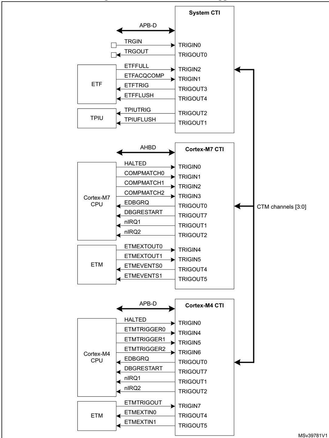
The diagram illustrates the Embedded cross trigger (CT) architecture. It features three main Control and Trigger Interface (CTI) blocks: System CTI, Cortex-M7 CTI, and Cortex-M4 CTI. Each CTI has multiple trigger inputs (TRIGIN) and trigger outputs (TRIGOUT). The System CTI is connected to an external trigger input (TRGIN) and output (TRGOUT), an Event Filter (ETF) via ETFFULL, ETFACQCOMP, ETFTRIG, and ETFFLUSH signals, and a Trace Port Interface Unit (TPIU) via TPIUTRIG and TPIUFLUSH signals. The Cortex-M7 CTI is connected to the Cortex-M7 CPU via HALTED, COMPMATCH0-2, EDBGREQ, DBGRESTART, nIRQ1, and nIRQ2 signals, and to an ETM via ETMEXTOUT0-1, ETMEVENTS0-1 signals. The Cortex-M4 CTI is connected to the Cortex-M4 CPU via HALTED, ETMTRIGGER0-2, EDBGREQ, DBGRESTART, nIRQ1, and nIRQ2 signals, and to an ETM via ETMTRIGOUT, ETMEXTIN0-1 signals. All three CTIs are interconnected via a common set of CTM channels [3:0]. The System CTI is connected to the APB-D bus, while the Cortex-M7 CTI is connected to the AHBD bus and the Cortex-M4 CTI is connected to the APB-D bus.
MSv39781V1
The CTIs allow events from various sources to trigger debug and/or trace activity. For example, a breakpoint reached in one of the processor cores can stop the other processor, or a transition detected on an external trigger input can start code trace.
Each CTI has up to 8 trigger inputs and 8 trigger outputs. Any input can be connected to any output, on the same CTI, or on another CTI via the CTM.
The trigger input and output signals for each CTI are listed in Table 630 to Table 635 .
Table 630. System CTI inputs
| # | Source signal | Source component | Comments |
|---|---|---|---|
| 0 | DBTRIGI | GPIO | External trigger input - allows an external signal to generate a debug event |
| 1 | ETFACQCOMP | ETF | ETF capture finished - allows a debug event to be generated when the trace FIFO is empty |
| 2 | ETFFULL | ETF | ETF full flag - allows a debug event to be generated when the trace FIFO is full |
| 3 | - | - | Not used |
| 4 | - | - | Not used |
| 5 | - | - | Not used |
| 6 | - | - | Not used |
| 7 | - | - | Not used |
Table 631. System CTI outputs
| # | Output signal | Destination component | Comments |
|---|---|---|---|
| 0 | DBTRIGO | GPIO | External IO trigger output - allows monitoring of events on the external DBTRIGO pin |
| 1 | TPIUFLUSH | TPIU | Trace port flush trigger - causes the TPIU FIFO to be flushed |
| 2 | TPIUTRIG | TPIU | Trace Port enable trigger - starts trace output on the external trace port |
| 3 | ETFTRIG | ETF | ETF enable trigger - starts filling the Trace FIFO |
| 4 | ETFFLUSH | ETF | ETF flush trigger - causes the Trace FIFO to be flushed |
| 5 | - | - | Not used |
| 6 | - | - | Not used |
| 7 | - | - | Not used |
Table 632. Cortex-M7 CTI inputs
| # | Source signal | Source component | Comments |
|---|---|---|---|
| 0 | HALTED | Cortex-M7 CPU | CPU halted - indicates CPU is in Debug mode |
| 1 | COMPMATCH0 | Cortex-M7 DWT | DWT comparator 0 match |
| 2 | COMPMATCH1 | Cortex-M7 DWT | DWT comparator 1 match |
| 3 | COMPMATCH2 | Cortex-M7 DWT | DWT comparator 2 match |
| 4 | ETMEXTOUT0 | Cortex-M7 ETM | ETM external trigger out |
| # | Source signal | Source component | Comments |
|---|---|---|---|
| 5 | ETMEXTOUT1 | Cortex-M7 ETM | ETM external trigger out |
| 6 | - | - | Not used |
| 7 | - | - | Not used |
| # | Output signal | Destination component | Comments |
|---|---|---|---|
| 0 | EDBGRQ | Cortex-M7 CPU | CPU halt request - puts CPU in Debug mode |
| 1 | nIRQ1 | Cortex-M7 NVIC | Interrupt request |
| 2 | nIRQ2 | Cortex-M7 NVIC | Interrupt request |
| 3 | - | - | Not used |
| 4 | ETMEVENTS0 | Cortex-M7 ETM | ETM trig request - enables CPU execution trace |
| 5 | ETMEVENTS1 | Cortex-M7 ETM | ETM trig request - enables CPU execution trace |
| 6 | - | - | Not used |
| 7 | DBGRESTART | Cortex-M7 CPU | CPU restart request - CPU exits Debug mode |
| # | Source signal | Source component | Comments |
|---|---|---|---|
| 0 | HALTED | M4 CPU | CPU halted - indicates CPU is in Debug mode |
| 1 | - | - | Not used |
| 2 | - | - | Not used |
| 3 | - | - | Not used |
| 4 | ETMTRIGGER0 | M4 DWT | Trace trigger - enables CPU execution trace |
| 5 | ETMTRIGGER1 | M4 DWT | Trace trigger - enables CPU execution trace |
| 6 | ETMTRIGGER2 | M4 DWT | Trace trigger - enables CPU execution trace |
| 7 | ETMTRIGOUT | M4 ETM | ETM triggered - indicates trace active |
| # | Output signal | Destination component | Comments |
|---|---|---|---|
| 0 | EDBGRQ | Cortex-M4 CPU | CPU halt request - puts CPU in Debug mode |
| 1 | nIRQ1 | Cortex-M4 NVIC | Interrupt request |
| 2 | nIRQ2 | Cortex-M4 NVIC | Interrupt request |
| 3 | - | - | Not used |
Table 635. Cortex-M4 CTI outputs (continued)
| # | Output signal | Destination component | Comments |
|---|---|---|---|
| 4 | ETMEXTIN0 | Cortex-M4 ETM | ETM trig request - enables CPU execution trace |
| 5 | ETMEXTIN1 | Cortex-M4 ETM | ETM trig request - enables CPU execution trace |
| 6 | - | - | Not used |
| 7 | DBGRESTART | Cortex-M4 CPU | CPU restart request - CPU exits Debug mode |
There are four event channels in the cross trigger matrix, which allows up to four parallel bidirectional connections between trigger inputs and outputs on different CTIs. To connect input number \( m \) on CTI \( x \) to output number \( n \) on CTI \( y \) , the input must be connected to an event channel \( p \) using the CTIINEN \( m \) register of CTI \( x \) . The same channel \( p \) must be connected to the output using the CTIOUTEN \( n \) register of CTI \( y \) . Note: this applies even if the input and output belong to the same CTI.
An input can be connected to more than one channel (up to four), so an input can be routed to several outputs. Similarly, an output can be connected to several inputs. It is also possible to connect several inputs/outputs to the same channel.
Figure 879. Mapping of trigger inputs to outputs
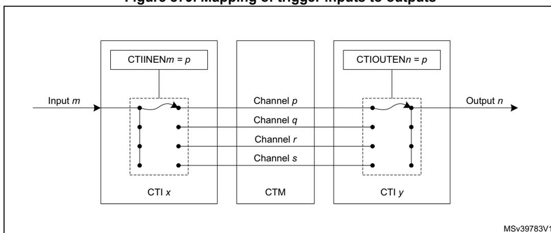
The diagram shows the internal architecture of the Cross Trigger Matrix (CTM) for mapping trigger inputs to outputs. It consists of three main components: CTI \( x \) , CTM, and CTI \( y \) .
- CTI \( x \) (Left): Contains an input \( m \) and a register CTIINEN \( m = p \) . A dashed box highlights the internal switch mechanism that connects the input to a specific channel in the CTM.
- CTM (Center): Contains four channels labeled Channel \( p \) , Channel \( q \) , Channel \( r \) , and Channel \( s \) . These channels act as a bus for triggering signals.
- CTI \( y \) (Right): Contains an output \( n \) and a register CTIOUTEN \( n = p \) . A dashed box highlights the internal switch mechanism that connects a specific channel from the CTM to the output.
The diagram shows that Input \( m \) from CTI \( x \) is connected via a switch to Channel \( p \) in the CTM. Channel \( p \) is then connected via another switch in CTI \( y \) to Output \( n \) . The other channels ( \( q \) , \( r \) , \( s \) ) are shown but not connected to any output in this example. The label MSV39783V1 is present in the bottom right corner.
Example configurations:
When either CPU core hits a breakpoint, stop the other core. Restart the two cores synchronously.
To stop both cores when either core stops requires the HALTED output of each core to be connected to the EDBGREQ input of the opposite core.
As shown in Table 632 and Table 634 , the HALTED signal from the Cortex-M7 core is connected to input 0 of the Cortex-M7 CTI, and the same signal from the Cortex-M4 core is connected to the same input on the Cortex-M4 CTI. Hence the CTIINEN0 register on each CTI is programmed such as to connect these inputs to a CTM channel (for example channel 0).
As shown in Table 633 and Table 635 , the EDBGGRQ signals to the CPUs are connected to output 0 of the respective CTIs. Therefore, the CTIOUTEN0 register of the each CTI should be programmed such as to connect these outputs to the same CTM channel.
To restart both cores simultaneously the debugger must use the APPPULSE register in either of the CTIs. This allows the debugger to generate a pulse on any of the four ETM channels. The channel must be connected to the DBGRESTART signal of both cores.
As shown in Table 633 and Table 635 , the DBGRESTART signals to the CPUs are connected to output 1 of the respective CTIs. Therefore, the CTIOUTEN1 register of the each CTI should be programmed such as to connect these outputs to an unused CTM channel (for example channel 1).
The above configuration is illustrated in Figure 880 .
Figure 880. Cross trigger configuration example
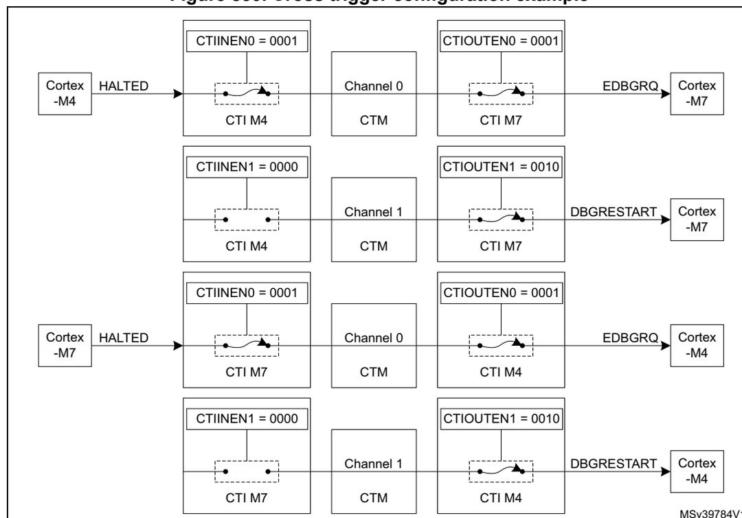
To force the processors to restart simultaneously, the debugger should use the following procedure:
- 1. Clear the debug request by writing 0x01, then 0x00, to the CTIINTACK register in each CTI.
- 2. Cause a pulse on channel 1 by writing 0x02 to the APPPULSE register in either CTI. This will generate a restart request to both processors.
Note that the debugger can also force both cores to stop simultaneously by writing 0x01 to the APPPULSE register in either CTI, which generates a pulse on channel 0.
For more information on the cross-trigger interface CoreSight component, refer to the Arm® CoreSight™ SoC-400 Technical Reference Manual [2] .
CTI registers
The register file base address for each CTI is defined by the ROM table for the bus to which it is connected. The registers are the same for each CTI.
CTI control register (CTI_CONTROL)
Address offset: 0x000
Reset value: 0x0000 0000
| 31 | 30 | 29 | 28 | 27 | 26 | 25 | 24 | 23 | 22 | 21 | 20 | 19 | 18 | 17 | 16 |
|---|---|---|---|---|---|---|---|---|---|---|---|---|---|---|---|
| Res. | Res. | Res. | Res. | Res. | Res. | Res. | Res. | Res. | Res. | Res. | Res. | Res. | Res. | Res. | Res. |
| 15 | 14 | 13 | 12 | 11 | 10 | 9 | 8 | 7 | 6 | 5 | 4 | 3 | 2 | 1 | 0 |
| Res. | Res. | Res. | Res. | Res. | Res. | Res. | Res. | Res. | Res. | Res. | Res. | Res. | Res. | Res. | GLBEN |
| rw |
Bits 31:1 Reserved, must be kept at reset value.
Bit 0 GLBEN : Global enable.
0: Cross-triggering disabled
1: Cross-triggering enabled
CTI trigger acknowledge register (CTI_INTACK)
Address offset: 0x010
Reset value: 0x0000 0000
| 31 | 30 | 29 | 28 | 27 | 26 | 25 | 24 | 23 | 22 | 21 | 20 | 19 | 18 | 17 | 16 |
|---|---|---|---|---|---|---|---|---|---|---|---|---|---|---|---|
| Res. | Res. | Res. | Res. | Res. | Res. | Res. | Res. | Res. | Res. | Res. | Res. | Res. | Res. | Res. | Res. |
| 15 | 14 | 13 | 12 | 11 | 10 | 9 | 8 | 7 | 6 | 5 | 4 | 3 | 2 | 1 | 0 |
| Res. | Res. | Res. | Res. | Res. | Res. | Res. | Res. | INTACK[7:0] | |||||||
| rw | rw | rw | rw | rw | rw | rw | rw | ||||||||
Bits 31:8 Reserved, must be kept at reset value.
Bits 7:0 INTACK[7:0] : Trigger acknowledge
There is one bit of the register for each CTITRIGOUT output. When a 1 is written to a bit in this register, the corresponding CTITRIGOUT output is acknowledged, causing it to be cleared.
CTI application trigger set register (CTI_APPSET)
Address offset: 0x014
Reset value: 0x0000 0000
| 31 | 30 | 29 | 28 | 27 | 26 | 25 | 24 | 23 | 22 | 21 | 20 | 19 | 18 | 17 | 16 |
|---|---|---|---|---|---|---|---|---|---|---|---|---|---|---|---|
| Res. | Res. | Res. | Res. | Res. | Res. | Res. | Res. | Res. | Res. | Res. | Res. | Res. | Res. | Res. | Res. |
| 15 | 14 | 13 | 12 | 11 | 10 | 9 | 8 | 7 | 6 | 5 | 4 | 3 | 2 | 1 | 0 |
| Res. | Res. | Res. | Res. | Res. | Res. | Res. | Res. | Res. | Res. | Res. | Res. | APPSET[3:0] | |||
| rw | rw | rw | rw | ||||||||||||
Bits 31:4 Reserved, must be kept at reset value.
Bits 3:0 APPSET[3:0] : Set channel event
Read:
- 0bXXX0: Channel 0 event inactive
- 0bXXX1: Channel 0 event active
- 0bXX0X: Channel 1 event inactive
- 0bXX1X: Channel 1 event active
- 0bX0XX: Channel 2 event inactive
- 0bX1XX: Channel 2 event active
- 0b0XXX: Channel 3 event inactive
- 0b1XXX: Channel 3 event active
Write:
- 0bXXX0: No effect
- 0bXXX1: Set event on Channel 0
- 0bXX0X: No effect
- 0bXX1X: Set event on Channel 1
- 0bX0XX: No effect
- 0bX1XX: Set event on Channel 2
- 0b0XXX: No effect
- 0b1XXX: Set event on Channel 3
CTI application trigger clear register (CTI_APPCLEAR)
Address offset: 0x018
Reset value: 0x0000 0000
| 31 | 30 | 29 | 28 | 27 | 26 | 25 | 24 | 23 | 22 | 21 | 20 | 19 | 18 | 17 | 16 |
|---|---|---|---|---|---|---|---|---|---|---|---|---|---|---|---|
| Res. | Res. | Res. | Res. | Res. | Res. | Res. | Res. | Res. | Res. | Res. | Res. | Res. | Res. | Res. | Res. |
| 15 | 14 | 13 | 12 | 11 | 10 | 9 | 8 | 7 | 6 | 5 | 4 | 3 | 2 | 1 | 0 |
| Res. | Res. | Res. | Res. | Res. | Res. | Res. | Res. | Res. | Res. | Res. | Res. | APPCLEAR[3:0] | |||
| w | w | w | w | ||||||||||||
Bits 31:4 Reserved, must be kept at reset value.
Bits 3:0 APPCLEAR[3:0] : Clear channel event
0bXXX0: No effect
0bXXX1: Clear event on Channel 0
0bXX0X: No effect
0bXX1X: Clear event on Channel 1
0bX0XX: No effect
0bX1XX: Clear event on Channel 2
0b0XXX: No effect
0b1XXX: Clear event on Channel 3
CTI application pulse register (CTI_APPPULSE)
Address offset: 0x01C
Reset value: 0x0000 0000
| 31 | 30 | 29 | 28 | 27 | 26 | 25 | 24 | 23 | 22 | 21 | 20 | 19 | 18 | 17 | 16 |
|---|---|---|---|---|---|---|---|---|---|---|---|---|---|---|---|
| Res. | Res. | Res. | Res. | Res. | Res. | Res. | Res. | Res. | Res. | Res. | Res. | Res. | Res. | Res. | Res. |
| 15 | 14 | 13 | 12 | 11 | 10 | 9 | 8 | 7 | 6 | 5 | 4 | 3 | 2 | 1 | 0 |
| Res. | Res. | Res. | Res. | Res. | Res. | Res. | Res. | Res. | Res. | Res. | Res. | APPPULSE[3:0] | |||
| w | w | w | w | ||||||||||||
Bits 31:4 Reserved, must be kept at reset value.
Bits 3:0 APPPULSE[3:0] : Pulse channel event
This register clears itself immediately.
0bXXX0: No effect
0bXXX1: Generate pulse on Channel 0
0bXX0X: No effect
0bXX1X: Generate pulse on Channel 1
0bX0XX: No effect
0bX1XX: Generate pulse on Channel 2
0b0XXX: No effect
0b1XXX: Generate pulse on Channel 3
CTI trigger IN x enable register (CTI_INENx)
Address offset: 0x020 + 4 * x, where x = 0 to 7
Reset value: 0x0000 0000
| 31 | 30 | 29 | 28 | 27 | 26 | 25 | 24 | 23 | 22 | 21 | 20 | 19 | 18 | 17 | 16 |
|---|---|---|---|---|---|---|---|---|---|---|---|---|---|---|---|
| Res. | Res. | Res. | Res. | Res. | Res. | Res. | Res. | Res. | Res. | Res. | Res. | Res. | Res. | Res. | Res. |
| 15 | 14 | 13 | 12 | 11 | 10 | 9 | 8 | 7 | 6 | 5 | 4 | 3 | 2 | 1 | 0 |
| Res. | Res. | Res. | Res. | Res. | Res. | Res. | Res. | Res. | Res. | Res. | Res. | TRIGINEN[3:0] | |||
| rw | rw | rw | rw | ||||||||||||
Bits 31:4 Reserved, must be kept at reset value.
Bits 3:0 TRIGINEN[3:0] : Cross-trigger event enable
Enables or disables a cross-trigger event on each of the four channels when CTITRIGINx is activated (x = 0 to 7).
- 0bXXX0: Trigger n does not generate events on Channel 0
- 0bXXX1: Trigger n generates events on Channel 0
- 0bXX0X: Trigger n does not generate events on Channel 1
- 0bXX1X: Trigger n generates events on Channel 1
- 0bX0XX: Trigger n does not generate events on Channel 2
- 0bX1XX: Trigger n generates events on Channel 2
- 0b0XXX: Trigger n does not generate events on Channel 3
- 0b1XXX: Trigger n generates events on Channel 3
CTI trigger OUT x enable register (CTI_OUTENx)
Address offset: 0x0A0 + 4 * x, where x = 0 to 7
Reset value: 0x0000 0000
| 31 | 30 | 29 | 28 | 27 | 26 | 25 | 24 | 23 | 22 | 21 | 20 | 19 | 18 | 17 | 16 |
|---|---|---|---|---|---|---|---|---|---|---|---|---|---|---|---|
| Res. | Res. | Res. | Res. | Res. | Res. | Res. | Res. | Res. | Res. | Res. | Res. | Res. | Res. | Res. | Res. |
| 15 | 14 | 13 | 12 | 11 | 10 | 9 | 8 | 7 | 6 | 5 | 4 | 3 | 2 | 1 | 0 |
| Res. | Res. | Res. | Res. | Res. | Res. | Res. | Res. | Res. | Res. | Res. | Res. | TRIGOUTEN[3:0] | |||
| rw | rw | rw | rw | ||||||||||||
Bits 31:4 Reserved, must be kept at reset value.
Bits 3:0 TRIGOUTEN[3:0] : Enable trigger upon event
For each channel, the field defines whether an event on that channel will generate a trigger on CTITRIGOUTx (x = 0 to 7).
- 0bXXX0: Channel 0 events do not generate triggers on Trigger output n
- 0bXXX1: Channel 0 events generate triggers on Trigger output n
- 0bXX0X: Channel 1 events do not generate triggers on Trigger output n
- 0bXX1X: Channel 1 events generate triggers on Trigger output n
- 0bX0XX: Channel 2 events do not generate triggers on Trigger output n
- 0bX1XX: Channel 2 events generate triggers on Trigger output n
- 0b0XXX: Channel 3 events do not generate triggers on Trigger output n
- 0b1XXX: Channel 3 events generate triggers on Trigger output n
CTI trigger IN status register (CTI_TRGISTS)
Address offset: 0x130
Reset value: 0x0000 0000
| 31 | 30 | 29 | 28 | 27 | 26 | 25 | 24 | 23 | 22 | 21 | 20 | 19 | 18 | 17 | 16 |
|---|---|---|---|---|---|---|---|---|---|---|---|---|---|---|---|
| Res. | Res. | Res. | Res. | Res. | Res. | Res. | Res. | Res. | Res. | Res. | Res. | Res. | Res. | Res. | Res. |
| 15 | 14 | 13 | 12 | 11 | 10 | 9 | 8 | 7 | 6 | 5 | 4 | 3 | 2 | 1 | 0 |
| Res. | Res. | Res. | Res. | Res. | Res. | Res. | Res. | TRIGINSTATUS[7:0] | |||||||
| r | r | r | r | r | r | r | r | ||||||||
Bits 31:8 Reserved, must be kept at reset value.
Bits 7:0 TRIGINSTATUS[7:0] : Trigger input status
There is one bit of the register for each CTITRIGIN input. When a bit is set to 1 it indicates that the corresponding trigger input is active. When it is set to 0, the corresponding trigger input is inactive.
CTI trigger OUT status register (CTI_TRGOSTS)
Address offset: 0x134
Reset value: 0x0000 0000
| 31 | 30 | 29 | 28 | 27 | 26 | 25 | 24 | 23 | 22 | 21 | 20 | 19 | 18 | 17 | 16 |
|---|---|---|---|---|---|---|---|---|---|---|---|---|---|---|---|
| Res. | Res. | Res. | Res. | Res. | Res. | Res. | Res. | Res. | Res. | Res. | Res. | Res. | Res. | Res. | Res. |
| 15 | 14 | 13 | 12 | 11 | 10 | 9 | 8 | 7 | 6 | 5 | 4 | 3 | 2 | 1 | 0 |
| Res. | Res. | Res. | Res. | Res. | Res. | Res. | Res. | TRIGOUTSTATUS[7:0] | |||||||
| r | r | r | r | r | r | r | r | ||||||||
Bits 31:8 Reserved, must be kept at reset value.
Bits 7:0 TRIGOUTSTATUS[7:0] : Trigger output status
There is one bit of the register for each CTITRIGOUT output. When a bit is set to 1 it indicates that the corresponding trigger output is active. When it is set to 0, the corresponding trigger output is inactive.
CTI channel IN status register (CTI_CHINSTS)
Address offset: 0x138
Reset value: 0x0000 0000
| 31 | 30 | 29 | 28 | 27 | 26 | 25 | 24 | 23 | 22 | 21 | 20 | 19 | 18 | 17 | 16 |
|---|---|---|---|---|---|---|---|---|---|---|---|---|---|---|---|
| Res. | Res. | Res. | Res. | Res. | Res. | Res. | Res. | Res. | Res. | Res. | Res. | Res. | Res. | Res. | Res. |
| 15 | 14 | 13 | 12 | 11 | 10 | 9 | 8 | 7 | 6 | 5 | 4 | 3 | 2 | 1 | 0 |
| Res. | Res. | Res. | Res. | Res. | Res. | Res. | Res. | Res. | Res. | Res. | Res. | CHINSTATUS[3:0] | |||
| r | r | r | r | ||||||||||||
Bits 31:4 Reserved, must be kept at reset value.
Bits 3:0 CHINSTATUS[3:0] : Channel input status
There is one bit of the register for each channel input. When a bit is set to 1 it indicates that the corresponding channel input is active. When it is set to 0, the corresponding channel input is inactive.
CTI channel OUT status register (CTI_CHOUTSTS)
Address offset: 0x13C
Reset value: 0x0000 0000
| 31 | 30 | 29 | 28 | 27 | 26 | 25 | 24 | 23 | 22 | 21 | 20 | 19 | 18 | 17 | 16 |
|---|---|---|---|---|---|---|---|---|---|---|---|---|---|---|---|
| Res. | Res. | Res. | Res. | Res. | Res. | Res. | Res. | Res. | Res. | Res. | Res. | Res. | Res. | Res. | Res. |
| 15 | 14 | 13 | 12 | 11 | 10 | 9 | 8 | 7 | 6 | 5 | 4 | 3 | 2 | 1 | 0 |
| Res. | Res. | Res. | Res. | Res. | Res. | Res. | Res. | Res. | Res. | Res. | Res. | CHOUTSTATUS[3:0] | |||
| r | r | r | r | ||||||||||||
Bits 31:4 Reserved, must be kept at reset value.
Bits 3:0 CHOUTSTATUS[3:0] : Channel output status
There is one bit of the register for each channel output. When a bit is set to 1 it indicates that the corresponding channel output is active. When it is set to 0, the corresponding channel output is inactive.
CTI channel gate register (CTI_GATE)
Address offset: 0x140
Reset value: 0x0000 000F
| 31 | 30 | 29 | 28 | 27 | 26 | 25 | 24 | 23 | 22 | 21 | 20 | 19 | 18 | 17 | 16 |
|---|---|---|---|---|---|---|---|---|---|---|---|---|---|---|---|
| Res. | Res. | Res. | Res. | Res. | Res. | Res. | Res. | Res. | Res. | Res. | Res. | Res. | Res. | Res. | Res. |
| 15 | 14 | 13 | 12 | 11 | 10 | 9 | 8 | 7 | 6 | 5 | 4 | 3 | 2 | 1 | 0 |
| Res. | Res. | Res. | Res. | Res. | Res. | Res. | Res. | Res. | Res. | Res. | Res. | GATEEN[3:0] | |||
| rw | rw | rw | rw | ||||||||||||
Bits 31:4 Reserved, must be kept at reset value.
Bits 3:0 GATEEN[3:0] : Channel output enable
For each channel, defines whether an event on that channel can propagate over the CTM to other CTIs.
0bXXX0: Channel 0 events do not propagate
0bXXX1: Channel 0 events propagate
0bXX0X: Channel 1 events do not propagate
0bXX1X: Channel 1 events propagate
0bX0XX: Channel 2 events do not propagate
0bX1XX: Channel 2 events propagate
0b0XXX: Channel 3 events do not propagate
0b1XXX: Channel 3 events propagate
CTI claim tag set register (CTI_CLAIMSET)
Address offset: 0xFA0
Reset value: 0x0000 000F
| 31 | 30 | 29 | 28 | 27 | 26 | 25 | 24 | 23 | 22 | 21 | 20 | 19 | 18 | 17 | 16 |
|---|---|---|---|---|---|---|---|---|---|---|---|---|---|---|---|
| Res. | Res. | Res. | Res. | Res. | Res. | Res. | Res. | Res. | Res. | Res. | Res. | Res. | Res. | Res. | Res. |
| 15 | 14 | 13 | 12 | 11 | 10 | 9 | 8 | 7 | 6 | 5 | 4 | 3 | 2 | 1 | 0 |
| Res. | Res. | Res. | Res. | Res. | Res. | Res. | Res. | Res. | Res. | Res. | Res. | CLAIMSET[3:0] | |||
| rw | rw | rw | rw | ||||||||||||
Bits 31:4 Reserved, must be kept at reset value.
Bits 3:0 CLAIMSET[3:0] : Set claim tag bits
Write:
0000: No effect
xxx1: Set bit 0
xx1x: Set bit 1
x1xx: Set bit 2
1xxx: Set bit 3
Read:
0xF: Indicates there are four bits in claim tag
CTI claim tag clear register (CTI_CLAIMCLR)
Address offset: 0xFA4
Reset value: 0x0000 0000
| 31 | 30 | 29 | 28 | 27 | 26 | 25 | 24 | 23 | 22 | 21 | 20 | 19 | 18 | 17 | 16 |
|---|---|---|---|---|---|---|---|---|---|---|---|---|---|---|---|
| Res. | Res. | Res. | Res. | Res. | Res. | Res. | Res. | Res. | Res. | Res. | Res. | Res. | Res. | Res. | Res. |
| 15 | 14 | 13 | 12 | 11 | 10 | 9 | 8 | 7 | 6 | 5 | 4 | 3 | 2 | 1 | 0 |
| Res. | Res. | Res. | Res. | Res. | Res. | Res. | Res. | Res. | Res. | Res. | Res. | CLAIMCLR[3:0] | |||
| rw | rw | rw | rw | ||||||||||||
Bits 31:4 Reserved, must be kept at reset value.
Bits 3:0 CLAIMCLR[3:0] : Reset claim tag bits
Write:
0000: No effect
xxx1: Clear bit 0
xx1x: Clear bit 1
x1xx: Clear bit 2
1xxx: Clear bit 3
Read: Returns current value of claim tag
CTI lock access register (CTI_LAR)
Address offset: 0xFB0
Reset value: N/A
| 31 | 30 | 29 | 28 | 27 | 26 | 25 | 24 | 23 | 22 | 21 | 20 | 19 | 18 | 17 | 16 |
|---|---|---|---|---|---|---|---|---|---|---|---|---|---|---|---|
| ACCESS_W[31:16] | |||||||||||||||
| w | w | w | w | w | w | w | w | w | w | w | w | w | w | w | w |
| 15 | 14 | 13 | 12 | 11 | 10 | 9 | 8 | 7 | 6 | 5 | 4 | 3 | 2 | 1 | 0 |
| ACCESS_W[15:0] | |||||||||||||||
| w | w | w | w | w | w | w | w | w | w | w | w | w | w | w | w |
Bits 31:0 ACCESS_W[31:0] : CTI register write access enable
Enables write access to some CTI registers by processor cores (debuggers do not need to unlock the component)
0xC5ACCE55: Enable write access
Other values: Disable write access
CTI lock status register (CTI_LSR)
Address offset: 0xFB4
Reset value: 0x0000 0003
| 31 | 30 | 29 | 28 | 27 | 26 | 25 | 24 | 23 | 22 | 21 | 20 | 19 | 18 | 17 | 16 |
|---|---|---|---|---|---|---|---|---|---|---|---|---|---|---|---|
| Res. | Res. | Res. | Res. | Res. | Res. | Res. | Res. | Res. | Res. | Res. | Res. | Res. | Res. | Res. | Res. |
| 15 | 14 | 13 | 12 | 11 | 10 | 9 | 8 | 7 | 6 | 5 | 4 | 3 | 2 | 1 | 0 |
| Res. | Res. | Res. | Res. | Res. | Res. | Res. | Res. | Res. | Res. | Res. | Res. | Res. | LOCKTYPE | LOCKGRANT | LOCKEXIST |
| r | r | r |
Bits 31:3 Reserved, must be kept at reset value.
Bit 2 LOCKTYPE : Size of the CTI_LAR register
0: 32-bit
Bit 1 LOCKGRANT : Current status of lock
This bit always returns zero when read by an external debugger.
0: Write access is permitted
1: Write access is blocked. Only read access is permitted.
Bit 0 LOCKEXIST : Existence of lock control mechanism
The bit indicates whether a lock control mechanism exists. It always returns zero when read by an external debugger.
0: No lock control mechanism exists
1: Lock control mechanism is implemented
CTI authentication status register (CTI_AUTHSTAT)
Address offset: 0xFB8
Reset value: 0x0000 000A
| 31 | 30 | 29 | 28 | 27 | 26 | 25 | 24 | 23 | 22 | 21 | 20 | 19 | 18 | 17 | 16 |
|---|---|---|---|---|---|---|---|---|---|---|---|---|---|---|---|
| Res. | Res. | Res. | Res. | Res. | Res. | Res. | Res. | Res. | Res. | Res. | Res. | Res. | Res. | Res. | Res. |
| 15 | 14 | 13 | 12 | 11 | 10 | 9 | 8 | 7 | 6 | 5 | 4 | 3 | 2 | 1 | 0 |
| Res. | Res. | Res. | Res. | Res. | Res. | Res. | Res. | SNID[1:0] | SID[1:0] | NSNID[1:0] | NSID[1:0] | ||||
| r | r | r | r | r | r | r | r |
Bits 31:8 Reserved, must be kept at reset value.
Bits 7:6
SNID[1:0]
: Security level for secure non-invasive debug
0x0: Not implemented
Bits 5:4
SID[1:0]
: Security level for secure invasive debug
0x0: Not implemented
Bits 3:2
NSNID[1:0]
: Security level for non-secure non-invasive debug
0x2: Disabled
0x3: Enabled
Bits 1:0
NSID[1:0]
: Security level for non-secure invasive debug
0x2: Disabled
0x3: Enabled
CTI device configuration register (CTI_DEVID)
Address offset: 0xFC8
Reset value: 0x0004 0800
| 31 | 30 | 29 | 28 | 27 | 26 | 25 | 24 | 23 | 22 | 21 | 20 | 19 | 18 | 17 | 16 |
|---|---|---|---|---|---|---|---|---|---|---|---|---|---|---|---|
| Res. | Res. | Res. | Res. | Res. | Res. | Res. | Res. | Res. | Res. | Res. | Res. | NUMCH[3:0] | |||
| r | r | r | r | ||||||||||||
| 15 | 14 | 13 | 12 | 11 | 10 | 9 | 8 | 7 | 6 | 5 | 4 | 3 | 2 | 1 | 0 |
| NUMTRIG[7:0] | Res. | Res. | Res. | EXTMUXNUM[4:0] | |||||||||||
| r | r | r | r | r | r | r | r | r | r | r | r | r | |||
Bits 31:20 Reserved, must be kept at reset value.
Bits 19:16
NUMCH[3:0]
: Number of ECT channels available
0x4: 4 channels
Bits 15:8
NUMTRIG[7:0]
: Number of ECT triggers available
0x8: 8 trigger inputs and 8 trigger outputs
Bits 7:5 Reserved, must be kept at reset value.
Bits 4:0
EXTMUXNUM[4:0]
: Number of trigger input/output multiplexers
0x0: None
CTI device type identifier register (CTI_DEVTYPE)
Address offset: 0xFCC
Reset value: 0x0000 0014
| 31 | 30 | 29 | 28 | 27 | 26 | 25 | 24 | 23 | 22 | 21 | 20 | 19 | 18 | 17 | 16 |
|---|---|---|---|---|---|---|---|---|---|---|---|---|---|---|---|
| Res. | Res. | Res. | Res. | Res. | Res. | Res. | Res. | Res. | Res. | Res. | Res. | Res. | Res. | Res. | Res. |
| 15 | 14 | 13 | 12 | 11 | 10 | 9 | 8 | 7 | 6 | 5 | 4 | 3 | 2 | 1 | 0 |
| Res. | Res. | Res. | Res. | Res. | Res. | Res. | Res. | SUBTYPE[3:0] | MAJORTYPE[3:0] | ||||||
| r | r | r | r | r | r | r | r | ||||||||
Bits 31:8 Reserved, must be kept at reset value.
Bits 7:4 SUBTYPE[3:0] : Sub-classification
0x1: Indicates that this component is a cross-triggering component.
Bits 3:0 MAJORTYPE[3:0] : Major classification
0x4: Indicates that this component allows a debugger to control other components in a CoreSight SoC-400 system.
CTI CoreSight peripheral identity register 4 (CTI_PIDR4)
Address offset: 0xFD0
Reset value: 0x0000 0004
| 31 | 30 | 29 | 28 | 27 | 26 | 25 | 24 | 23 | 22 | 21 | 20 | 19 | 18 | 17 | 16 |
|---|---|---|---|---|---|---|---|---|---|---|---|---|---|---|---|
| Res. | Res. | Res. | Res. | Res. | Res. | Res. | Res. | Res. | Res. | Res. | Res. | Res. | Res. | Res. | Res. |
| 15 | 14 | 13 | 12 | 11 | 10 | 9 | 8 | 7 | 6 | 5 | 4 | 3 | 2 | 1 | 0 |
| Res. | Res. | Res. | Res. | Res. | Res. | Res. | Res. | 4KCOUNT[3:0] | JEP106CON[3:0] | ||||||
| r | r | r | r | r | r | r | r | ||||||||
Bits 31:8 Reserved, must be kept at reset value.
Bits 7:4 4KCOUNT[3:0] : Register file size
0x0: Register file occupies a single 4 Kbyte region
Bits 3:0 JEP106CON[3:0] : JEP106 continuation code
0x4: Arm® JEDEC code
CTI CoreSight peripheral identity register 0 (CTI_PIDR0)
Address offset: 0xFE0
Reset value: 0x0000 0006
| 31 | 30 | 29 | 28 | 27 | 26 | 25 | 24 | 23 | 22 | 21 | 20 | 19 | 18 | 17 | 16 |
|---|---|---|---|---|---|---|---|---|---|---|---|---|---|---|---|
| Res. | Res. | Res. | Res. | Res. | Res. | Res. | Res. | Res. | Res. | Res. | Res. | Res. | Res. | Res. | Res. |
| 15 | 14 | 13 | 12 | 11 | 10 | 9 | 8 | 7 | 6 | 5 | 4 | 3 | 2 | 1 | 0 |
| Res. | Res. | Res. | Res. | Res. | Res. | Res. | Res. | PARTNUM[7:0] | |||||||
| r | r | r | r | r | r | r | r | ||||||||
Bits 31:8 Reserved, must be kept at reset value.
Bits 7:0 PARTNUM[7:0] : Part number field, bits [7:0]
0x06: CTI part number
CTI CoreSight peripheral identity register 1 (CTI_PIDR1)
Address offset: 0xFE4
Reset value: 0x0000 00B9
| 31 | 30 | 29 | 28 | 27 | 26 | 25 | 24 | 23 | 22 | 21 | 20 | 19 | 18 | 17 | 16 |
|---|---|---|---|---|---|---|---|---|---|---|---|---|---|---|---|
| Res. | Res. | Res. | Res. | Res. | Res. | Res. | Res. | Res. | Res. | Res. | Res. | Res. | Res. | Res. | Res. |
| 15 | 14 | 13 | 12 | 11 | 10 | 9 | 8 | 7 | 6 | 5 | 4 | 3 | 2 | 1 | 0 |
| Res. | Res. | Res. | Res. | Res. | Res. | Res. | Res. | JEP106ID[3:0] | PARTNUM[11:8] | ||||||
| r | r | r | r | r | r | r | r | ||||||||
Bits 31:8 Reserved, must be kept at reset value.
Bits 7:4 JEP106ID[3:0] : JEP106 identity code field, bits [3:0]
0xB: Arm ® JEDEC code
Bits 3:0 PARTNUM[11:8] : Part number field, bits [11:8]
0x9: CTI part number
CTI CoreSight peripheral identity register 2 (CTI_PIDR2)
Address offset: 0xFE8
Reset value: 0x0000 005B
| 31 | 30 | 29 | 28 | 27 | 26 | 25 | 24 | 23 | 22 | 21 | 20 | 19 | 18 | 17 | 16 |
|---|---|---|---|---|---|---|---|---|---|---|---|---|---|---|---|
| Res. | Res. | Res. | Res. | Res. | Res. | Res. | Res. | Res. | Res. | Res. | Res. | Res. | Res. | Res. | Res. |
| 15 | 14 | 13 | 12 | 11 | 10 | 9 | 8 | 7 | 6 | 5 | 4 | 3 | 2 | 1 | 0 |
| Res. | Res. | Res. | Res. | Res. | Res. | Res. | Res. | REVISION[3:0] | JEDEC | JEP106ID[6:4] | |||||
| r | r | r | r | r | r | r | r | ||||||||
Bits 31:8 Reserved, must be kept at reset value.
Bits 7:4 REVISION[3:0] : Component revision number
0x5: r1p0
Bit 3 JEDEC : JEDEC assigned value
1: Designer ID specified by JEDEC
Bits 2:0 JEP106ID[6:4] : JEP106 identity code field, bits [6:4]
0x3: Arm ® JEDEC code
CTI CoreSight peripheral identity register 3 (CTI_PIDR3)
Address offset: 0xFEC
Reset value: 0x0000 0000
| 31 | 30 | 29 | 28 | 27 | 26 | 25 | 24 | 23 | 22 | 21 | 20 | 19 | 18 | 17 | 16 |
|---|---|---|---|---|---|---|---|---|---|---|---|---|---|---|---|
| Res. | Res. | Res. | Res. | Res. | Res. | Res. | Res. | Res. | Res. | Res. | Res. | Res. | Res. | Res. | Res. |
| 15 | 14 | 13 | 12 | 11 | 10 | 9 | 8 | 7 | 6 | 5 | 4 | 3 | 2 | 1 | 0 |
| Res. | Res. | Res. | Res. | Res. | Res. | Res. | Res. | REVAND[3:0] | CMOD[3:0] | ||||||
| r | r | r | r | r | r | r | r | ||||||||
Bits 31:8 Reserved, must be kept at reset value.
Bits 7:4 REVAND[3:0] : Metal fix version
0x0: No metal fix
Bits 3:0 CMOD[3:0] : Customer modified
0x0: No customer modifications
CTI CoreSight component identity register 0 (CTI_CIDR0)
Address offset: 0xFF0
Reset value: 0x0000 000D
| 31 | 30 | 29 | 28 | 27 | 26 | 25 | 24 | 23 | 22 | 21 | 20 | 19 | 18 | 17 | 16 |
|---|---|---|---|---|---|---|---|---|---|---|---|---|---|---|---|
| Res. | Res. | Res. | Res. | Res. | Res. | Res. | Res. | Res. | Res. | Res. | Res. | Res. | Res. | Res. | Res. |
| 15 | 14 | 13 | 12 | 11 | 10 | 9 | 8 | 7 | 6 | 5 | 4 | 3 | 2 | 1 | 0 |
| Res. | Res. | Res. | Res. | Res. | Res. | Res. | Res. | PREAMBLE[7:0] | |||||||
| r | r | r | r | r | r | r | r | ||||||||
Bits 31:8 Reserved, must be kept at reset value.
Bits 7:0 PREAMBLE[7:0] : Component ID field, bits [7:0]
0x0D: Common ID value
CTI CoreSight component identity register 1 (CTI_CIDR1)
Address offset: 0xFF4
Reset value: 0x0000 0090
| 31 | 30 | 29 | 28 | 27 | 26 | 25 | 24 | 23 | 22 | 21 | 20 | 19 | 18 | 17 | 16 |
|---|---|---|---|---|---|---|---|---|---|---|---|---|---|---|---|
| Res. | Res. | Res. | Res. | Res. | Res. | Res. | Res. | Res. | Res. | Res. | Res. | Res. | Res. | Res. | Res. |
| 15 | 14 | 13 | 12 | 11 | 10 | 9 | 8 | 7 | 6 | 5 | 4 | 3 | 2 | 1 | 0 |
| Res. | Res. | Res. | Res. | Res. | Res. | Res. | Res. | CLASS[3:0] | PREAMBLE[11:8] | ||||||
| r | r | r | r | r | r | r | r | ||||||||
Bits 31:8 Reserved, must be kept at reset value.
Bits 7:4
CLASS[3:0]
: Component ID field, bits [15:12] - component class
0x9: CoreSight component
Bits 3:0
PREAMBLE[11:8]
: Component ID field, bits [11:8]
0x0: Common ID value
CTI CoreSight component identity register 2 (CTI_CIDR2)
Address offset: 0xFF8
Reset value: 0x0000 0005
| 31 | 30 | 29 | 28 | 27 | 26 | 25 | 24 | 23 | 22 | 21 | 20 | 19 | 18 | 17 | 16 |
|---|---|---|---|---|---|---|---|---|---|---|---|---|---|---|---|
| Res. | Res. | Res. | Res. | Res. | Res. | Res. | Res. | Res. | Res. | Res. | Res. | Res. | Res. | Res. | Res. |
| 15 | 14 | 13 | 12 | 11 | 10 | 9 | 8 | 7 | 6 | 5 | 4 | 3 | 2 | 1 | 0 |
| Res. | Res. | Res. | Res. | Res. | Res. | Res. | Res. | PREAMBLE[19:12] | |||||||
| r | r | r | r | r | r | r | r | ||||||||
Bits 31:8 Reserved, must be kept at reset value.
Bits 7:0
PREAMBLE[19:12]
: Component ID field, bits [23:16]
0x05: Common ID value
CTI CoreSight component identity register 3 (CTI_CIDR3)
Address offset: 0xFFC
Reset value: 0x0000 00B1
| 31 | 30 | 29 | 28 | 27 | 26 | 25 | 24 | 23 | 22 | 21 | 20 | 19 | 18 | 17 | 16 |
|---|---|---|---|---|---|---|---|---|---|---|---|---|---|---|---|
| Res. | Res. | Res. | Res. | Res. | Res. | Res. | Res. | Res. | Res. | Res. | Res. | Res. | Res. | Res. | Res. |
| 15 | 14 | 13 | 12 | 11 | 10 | 9 | 8 | 7 | 6 | 5 | 4 | 3 | 2 | 1 | 0 |
| Res. | Res. | Res. | Res. | Res. | Res. | Res. | Res. | PREAMBLE[27:20] | |||||||
| r | r | r | r | r | r | r | r | ||||||||
Bits 31:8 Reserved, must be kept at reset value.
Bits 7:0
PREAMBLE[27:20]
: Component ID field, bits [31:24]
0xB1: Common ID value
CTI register map and reset values
Table 636. CTI register map and reset values
| Offset | Register name | 31 | 30 | 29 | 28 | 27 | 26 | 25 | 24 | 23 | 22 | 21 | 20 | 19 | 18 | 17 | 16 | 15 | 14 | 13 | 12 | 11 | 10 | 9 | 8 | 7 | 6 | 5 | 4 | 3 | 2 | 1 | 0 | |
|---|---|---|---|---|---|---|---|---|---|---|---|---|---|---|---|---|---|---|---|---|---|---|---|---|---|---|---|---|---|---|---|---|---|---|
| 0x000 | CTI_CONTROL | Res. | Res. | Res. | Res. | Res. | Res. | Res. | Res. | Res. | Res. | Res. | Res. | Res. | Res. | Res. | Res. | Res. | Res. | Res. | Res. | Res. | Res. | Res. | Res. | Res. | Res. | Res. | Res. | Res. | Res. | Res. | Res. | GI.BEN |
| Reset value | 0 | |||||||||||||||||||||||||||||||||
| 0x010 | CTI_INTACK | Res. | Res. | Res. | Res. | Res. | Res. | Res. | Res. | Res. | Res. | Res. | Res. | Res. | Res. | Res. | Res. | Res. | Res. | Res. | Res. | Res. | Res. | Res. | Res. | Res. | Res. | Res. | Res. | Res. | Res. | Res. | INTACK[7:0] | |
| Reset value | 0 0 0 0 0 0 0 0 | |||||||||||||||||||||||||||||||||
| 0x014 | CTI_APPSET | Res. | Res. | Res. | Res. | Res. | Res. | Res. | Res. | Res. | Res. | Res. | Res. | Res. | Res. | Res. | Res. | Res. | Res. | Res. | Res. | Res. | Res. | Res. | Res. | Res. | Res. | Res. | Res. | Res. | Res. | Res. | APPSET[3:0] | |
| Reset value | 0 0 0 0 | |||||||||||||||||||||||||||||||||
| 0x018 | CTI_APPCLEAR | Res. | Res. | Res. | Res. | Res. | Res. | Res. | Res. | Res. | Res. | Res. | Res. | Res. | Res. | Res. | Res. | Res. | Res. | Res. | Res. | Res. | Res. | Res. | Res. | Res. | Res. | Res. | Res. | Res. | Res. | Res. | APPCLEAR[3:0] | |
| Reset value | 0 0 0 0 | |||||||||||||||||||||||||||||||||
| 0x01C | CTI_APPPULSE | Res. | Res. | Res. | Res. | Res. | Res. | Res. | Res. | Res. | Res. | Res. | Res. | Res. | Res. | Res. | Res. | Res. | Res. | Res. | Res. | Res. | Res. | Res. | Res. | Res. | Res. | Res. | Res. | Res. | Res. | Res. | APPULSE[3:0] | |
| Reset value | 0 0 0 0 | |||||||||||||||||||||||||||||||||
| 0x020 to 0x03C | CTI_INEN0 to CTI_INEN7 | Res. | Res. | Res. | Res. | Res. | Res. | Res. | Res. | Res. | Res. | Res. | Res. | Res. | Res. | Res. | Res. | Res. | Res. | Res. | Res. | Res. | Res. | Res. | Res. | Res. | Res. | Res. | Res. | Res. | Res. | Res. | TRIGINEN[3:0] | |
| Reset value | 0 0 0 0 | |||||||||||||||||||||||||||||||||
| 0x040 to 0x09C | Reserved | Reserved | ||||||||||||||||||||||||||||||||
| 0x0A0 to 0x0BC | CTI_OUTEN0 to CTI_OUTEN7 | Res. | Res. | Res. | Res. | Res. | Res. | Res. | Res. | Res. | Res. | Res. | Res. | Res. | Res. | Res. | Res. | Res. | Res. | Res. | Res. | Res. | Res. | Res. | Res. | Res. | Res. | Res. | Res. | Res. | Res. | Res. | TRIGOUTEN[3:0] | |
| Reset value | 0 0 0 0 | |||||||||||||||||||||||||||||||||
| 0x0C0 to 0x12C | Reserved | Reserved | ||||||||||||||||||||||||||||||||
| 0x130 | CTI_TRIGISTS | Res. | Res. | Res. | Res. | Res. | Res. | Res. | Res. | Res. | Res. | Res. | Res. | Res. | Res. | Res. | Res. | Res. | Res. | Res. | Res. | Res. | Res. | Res. | Res. | Res. | Res. | Res. | Res. | Res. | Res. | Res. | TRIGINSTATUS[7:0] | |
| Reset value | 0 0 0 0 0 0 0 0 | |||||||||||||||||||||||||||||||||
| 0x134 | CTI_TRIGOSTS | Res. | Res. | Res. | Res. | Res. | Res. | Res. | Res. | Res. | Res. | Res. | Res. | Res. | Res. | Res. | Res. | Res. | Res. | Res. | Res. | Res. | Res. | Res. | Res. | Res. | Res. | Res. | Res. | Res. | Res. | Res. | TRIGOUTSTATUS[7:0] | |
| Reset value | 0 0 0 0 0 0 0 0 | |||||||||||||||||||||||||||||||||
| 0x138 | CTI_CHINSTS | Res. | Res. | Res. | Res. | Res. | Res. | Res. | Res. | Res. | Res. | Res. | Res. | Res. | Res. | Res. | Res. | Res. | Res. | Res. | Res. | Res. | Res. | Res. | Res. | Res. | Res. | Res. | Res. | Res. | Res. | Res. | CHISTATUS[3:0] | |
| Reset value | 0 0 0 0 | |||||||||||||||||||||||||||||||||
| 0x13C | CTI_CHOUTSTS | Res. | Res. | Res. | Res. | Res. | Res. | Res. | Res. | Res. | Res. | Res. | Res. | Res. | Res. | Res. | Res. | Res. | Res. | Res. | Res. | Res. | Res. | Res. | Res. | Res. | Res. | Res. | Res. | Res. | Res. | Res. | CHOSTATUS[3:0] | |
| Reset value | 0 0 0 0 | |||||||||||||||||||||||||||||||||
| 0x140 | CTI_GATE | Res. | Res. | Res. | Res. | Res. | Res. | Res. | Res. | Res. | Res. | Res. | Res. | Res. | Res. | Res. | Res. | Res. | Res. | Res. | Res. | Res. | Res. | Res. | Res. | Res. | Res. | Res. | Res. | Res. | Res. | Res. | GATEEN[3:0] | |
| Reset value | 1 1 1 1 | |||||||||||||||||||||||||||||||||
| 0x144 to 0xF9C | Reserved | Reserved | ||||||||||||||||||||||||||||||||
| 0xFA0 | CTI_CLAIMSET | Res. | Res. | Res. | Res. | Res. | Res. | Res. | Res. | Res. | Res. | Res. | Res. | Res. | Res. | Res. | Res. | Res. | Res. | Res. | Res. | Res. | Res. | Res. | Res. | Res. | Res. | Res. | Res. | Res. | Res. | Res. | CLAIMSET[3:0] | |
| Reset value | 1 1 1 1 | |||||||||||||||||||||||||||||||||
| 0xFA4 | CTI_CLAIMCLR | Res. | Res. | Res. | Res. | Res. | Res. | Res. | Res. | Res. | Res. | Res. | Res. | Res. | Res. | Res. | Res. | Res. | Res. | Res. | Res. | Res. | Res. | Res. | Res. | Res. | Res. | Res. | Res. | Res. | Res. | Res. | CLAIMCLR[3:0] | |
| Reset value | 0 0 0 0 | |||||||||||||||||||||||||||||||||
| 0xFA8 to 0xFAC | Reserved | Reserved | ||||||||||||||||||||||||||||||||
Table 636. CTI register map and reset values (continued)
| Offset | Register name | 31 | 30 | 29 | 28 | 27 | 26 | 25 | 24 | 23 | 22 | 21 | 20 | 19 | 18 | 17 | 16 | 15 | 14 | 13 | 12 | 11 | 10 | 9 | 8 | 7 | 6 | 5 | 4 | 3 | 2 | 1 | 0 |
|---|---|---|---|---|---|---|---|---|---|---|---|---|---|---|---|---|---|---|---|---|---|---|---|---|---|---|---|---|---|---|---|---|---|
| 0xFB0 | CTI_LAR | ACCESS_W[31:0] | |||||||||||||||||||||||||||||||
| Reset value | - | - | - | - | - | - | - | - | - | - | - | - | - | - | - | - | - | - | - | - | - | - | - | - | - | - | - | - | - | - | - | ||
| 0xFB4 | CTI_LSR | Res. | Res. | Res. | Res. | Res. | Res. | Res. | Res. | Res. | Res. | Res. | Res. | Res. | Res. | Res. | Res. | Res. | Res. | Res. | Res. | Res. | Res. | Res. | Res. | Res. | Res. | Res. | Res. | Res. | LOCKTYPE | LOCKGRANT | LOCKEXIST |
| Reset value | 0 | 1 | 1 | ||||||||||||||||||||||||||||||
| 0xFB8 | CTI_AUTHSTAT | Res. | Res. | Res. | Res. | Res. | Res. | Res. | Res. | Res. | Res. | Res. | Res. | Res. | Res. | Res. | Res. | Res. | Res. | Res. | Res. | Res. | Res. | Res. | Res. | SNID[1:0] | SI[1:0] | NSNID[1:0] | NSID[1:0] | ||||
| Reset value | 0 | 0 | 0 | 0 | 1 | 0 | 1 | 0 | |||||||||||||||||||||||||
| 0xFC8 | CTI_DEVID | Res. | Res. | Res. | Res. | Res. | Res. | Res. | Res. | Res. | Res. | Res. | Res. | NUMCH[3:0] | NUMTRIG[7:0] | Res. | Res. | Res. | EXMUXNUM[4:0] | ||||||||||||||
| Reset value | 0 | 1 | 0 | 0 | 0 | 0 | 0 | 0 | 1 | 0 | 0 | 0 | 0 | 0 | 0 | 0 | |||||||||||||||||
| 0xFC8 | CTI_DEVTYPE | Res. | Res. | Res. | Res. | Res. | Res. | Res. | Res. | Res. | Res. | Res. | Res. | Res. | Res. | Res. | Res. | Res. | Res. | Res. | Res. | Res. | Res. | Res. | Res. | SUBTYPE[3:0] | MAJORTYPE[3:0] | ||||||
| Reset value | 0 | 0 | 0 | 1 | 0 | 1 | 0 | 0 | |||||||||||||||||||||||||
| 0xFD0 | CTI_PIDR4 | Res. | Res. | Res. | Res. | Res. | Res. | Res. | Res. | Res. | Res. | Res. | Res. | Res. | Res. | Res. | Res. | Res. | Res. | Res. | Res. | Res. | Res. | Res. | Res. | 4KCOUNT[3:0] | JEP106CON[3:0] | ||||||
| Reset value | 0 | 0 | 0 | 0 | 0 | 1 | 0 | 0 | |||||||||||||||||||||||||
| 0xFD4 to 0xFDC | Reserved | Reserved | |||||||||||||||||||||||||||||||
| 0xFE0 | CTI_PIDR0 | Res. | Res. | Res. | Res. | Res. | Res. | Res. | Res. | Res. | Res. | Res. | Res. | Res. | Res. | Res. | Res. | Res. | Res. | Res. | Res. | Res. | Res. | Res. | Res. | PARTNUM[7:0] | |||||||
| Reset value | 0 | 0 | 0 | 0 | 0 | 1 | 1 | 0 | |||||||||||||||||||||||||
| 0xFE4 | CTI_PIDR1 | Res. | Res. | Res. | Res. | Res. | Res. | Res. | Res. | Res. | Res. | Res. | Res. | Res. | Res. | Res. | Res. | Res. | Res. | Res. | Res. | Res. | Res. | Res. | Res. | JEP106ID[3:0] | PARTNUM[11:8] | ||||||
| Reset value | 1 | 0 | 1 | 1 | 1 | 0 | 0 | 1 | |||||||||||||||||||||||||
| 0xFE8 | CTI_PIDR2 | Res. | Res. | Res. | Res. | Res. | Res. | Res. | Res. | Res. | Res. | Res. | Res. | Res. | Res. | Res. | Res. | Res. | Res. | Res. | Res. | Res. | Res. | Res. | Res. | REVISION[3:0] | JEDEC | JEP106ID[6:4] | |||||
| Reset value | 0 | 1 | 0 | 1 | 1 | 0 | 1 | 1 | |||||||||||||||||||||||||
| 0xFEC | CTI_PIDR3 | Res. | Res. | Res. | Res. | Res. | Res. | Res. | Res. | Res. | Res. | Res. | Res. | Res. | Res. | Res. | Res. | Res. | Res. | Res. | Res. | Res. | Res. | Res. | Res. | REVAND[3:0] | CMOD[3:0] | ||||||
| Reset value | 0 | 0 | 0 | 0 | 0 | 0 | 0 | 0 | |||||||||||||||||||||||||
| 0xFF0 | CTI_CIDR0 | Res. | Res. | Res. | Res. | Res. | Res. | Res. | Res. | Res. | Res. | Res. | Res. | Res. | Res. | Res. | Res. | Res. | Res. | Res. | Res. | Res. | Res. | Res. | Res. | PREAMBLE[7:0] | |||||||
| Reset value | 0 | 0 | 0 | 0 | 1 | 1 | 0 | 1 | |||||||||||||||||||||||||
| 0xFF4 | CTI_CIDR1 | Res. | Res. | Res. | Res. | Res. | Res. | Res. | Res. | Res. | Res. | Res. | Res. | Res. | Res. | Res. | Res. | Res. | Res. | Res. | Res. | Res. | Res. | Res. | Res. | CLASS[3:0] | PREAMBLE[11:8] | ||||||
| Reset value | 1 | 0 | 0 | 1 | 0 | 0 | 0 | 0 | |||||||||||||||||||||||||
| 0xFF8 | CTI_CIDR2 | Res. | Res. | Res. | Res. | Res. | Res. | Res. | Res. | Res. | Res. | Res. | Res. | Res. | Res. | Res. | Res. | Res. | Res. | Res. | Res. | Res. | Res. | Res. | Res. | PREAMBLE[19:12] | |||||||
| Reset value | 0 | 0 | 0 | 0 | 0 | 1 | 0 | 1 | |||||||||||||||||||||||||
| 0xFFC | CTI_CIDR3 | Res. | Res. | Res. | Res. | Res. | Res. | Res. | Res. | Res. | Res. | Res. | Res. | Res. | Res. | Res. | Res. | Res. | Res. | Res. | Res. | Res. | Res. | Res. | Res. | PREAMBLE[27:20] | |||||||
| Reset value | 1 | 0 | 1 | 1 | 0 | 0 | 0 | 1 | |||||||||||||||||||||||||
63.5.4 Trace funnel (CSTF)
The trace funnel is a CoreSight component that combines the ATB buses from four trace sources into one single ATB. The CSTF has four ATB slave ports, and one ATB master port. An arbiter selects the slave ports according to a programmable priority.
The slave ports are connected as follows:
- • S0: Cortex-M7 ETM
- • S1: Cortex-M7 ITM
- • S2: Cortex-M4 ETM
- • S3: Cortex-M4 ITM
The CSTF registers allow the slave ports to be individually enabled, and their priority settings to be configured. The priorities can be modified only when trace is disabled. The arbitration works as follows:
- • The arbiter selects the slave port with the highest assigned priority that has data valid
- • Up to min_hold_time transfers are passed from the selected slave to the master port, where min_hold_time is programmable in the CONTROL register.
- • A new arbitration is then performed
High priority should be assigned to slave ports connected to sources with a small amount of buffering, or where data loss can not be tolerated. Low priority should be assigned to less critical sources or those with large buffers.
For more information on the ATB Funnel CoreSight component, refer to the Arm® CoreSight™ SoC-400 Technical Reference Manual [2].
Trace funnel registers
CSTF control register (CSTF_CTRL)
Address offset: 0x000
Reset value: 0x0000 0300
| 31 | 30 | 29 | 28 | 27 | 26 | 25 | 24 | 23 | 22 | 21 | 20 | 19 | 18 | 17 | 16 |
|---|---|---|---|---|---|---|---|---|---|---|---|---|---|---|---|
| Res. | Res. | Res. | Res. | Res. | Res. | Res. | Res. | Res. | Res. | Res. | Res. | Res. | Res. | Res. | Res. |
| 15 | 14 | 13 | 12 | 11 | 10 | 9 | 8 | 7 | 6 | 5 | 4 | 3 | 2 | 1 | 0 |
| Res. | Res. | Res. | Res. | MIN_HOLD_TIME[3:0] | Res. | Res. | Res. | Res. | ENS3 | ENS2 | ENS1 | ENS0 | |||
| rw | rw | rw | rw | rw | rw | rw | rw | ||||||||
Bits 31:12 Reserved, must be kept at reset value.
Bits 11:8 MIN_HOLD_TIME[3:0] : Number of transactions between arbitrations.
0x0: 1 transaction
:
0xE: 15 transactions
0xF: Reserved
Bits 7:4 Reserved, must be kept at reset value.
Bit 3 ENS3 : S3 slave port enable
- 0: Disable port
- 1: Enable port
Bit 2 ENS2 : S2 slave port enable
- 0: Disable port
- 1: Enable port
Bit 1 ENS1 : S1 slave port enable
- 0: Disable port
- 1: Enable port
Bit 0 ENS0 : S0 slave port enable
- 0: Disable port
- 1: Enable port
CSTF priority register (CSTF_PRIORITY)
Address offset: 0x004
Reset value: 0x0000 0688
| 31 | 30 | 29 | 28 | 27 | 26 | 25 | 24 | 23 | 22 | 21 | 20 | 19 | 18 | 17 | 16 |
|---|---|---|---|---|---|---|---|---|---|---|---|---|---|---|---|
| Res. | Res. | Res. | Res. | Res. | Res. | Res. | Res. | Res. | Res. | Res. | Res. | Res. | Res. | Res. | Res. |
| 15 | 14 | 13 | 12 | 11 | 8 | 5 | 2 | ||||||||
| Res. | Res. | Res. | Res. | PRIPORT3[2:0] | PRIPORT2[2:0] | PRIPORT1[2:0] | PRIPORT0[2:0] | ||||||||
| rw | rw | rw | rw | rw | rw | rw | rw | rw | rw | rw | rw | ||||
Bits 31:12 Reserved, must be kept at reset value.
Bits 11:9 PRIPORT3[2:0] : S3 slave port priority
- 0: Highest priority
- :
- 7: Lowest priority
Bits 8:6 PRIPORT2[2:0] : S2 slave port priority
- 0: Highest priority
- :
- 7: Lowest priority
Bits 5:3 PRIPORT1[2:0] : S1 slave port priority
- 0: Highest priority
- :
- 7: Lowest priority
Bits 2:0 PRIPORT0[2:0] : S0 slave port priority
- 0: Highest priority
- :
- 7: Lowest priority
Address offset: 0xFA0
Reset value: 0x0000 000F
| 31 | 30 | 29 | 28 | 27 | 26 | 25 | 24 | 23 | 22 | 21 | 20 | 19 | 18 | 17 | 16 |
|---|---|---|---|---|---|---|---|---|---|---|---|---|---|---|---|
| Res. | Res. | Res. | Res. | Res. | Res. | Res. | Res. | Res. | Res. | Res. | Res. | Res. | Res. | Res. | Res. |
| 15 | 14 | 13 | 12 | 11 | 10 | 9 | 8 | 7 | 6 | 5 | 4 | 3 | 2 | 1 | 0 |
| Res. | Res. | Res. | Res. | Res. | Res. | Res. | Res. | Res. | Res. | Res. | Res. | CLAIMSET[3:0] | |||
| rw | rw | rw | rw | ||||||||||||
Bits 31:4 Reserved, must be kept at reset value.
Bits 3:0 CLAIMSET[3:0] : Set claim tag bitsWrite:
0000: No effect
xxx1: Set bit 0
xx1x: Set bit 1
x1xx: Set bit 2
1xxx: Set bit 3
Read:
0xF: Indicates there are four bits in claim tag
CSTF claim tag clear register (CSTF_CLAIMCLR)Address offset: 0xFA4
Reset value: 0x0000 0000
| 31 | 30 | 29 | 28 | 27 | 26 | 25 | 24 | 23 | 22 | 21 | 20 | 19 | 18 | 17 | 16 |
|---|---|---|---|---|---|---|---|---|---|---|---|---|---|---|---|
| Res. | Res. | Res. | Res. | Res. | Res. | Res. | Res. | Res. | Res. | Res. | Res. | Res. | Res. | Res. | Res. |
| 15 | 14 | 13 | 12 | 11 | 10 | 9 | 8 | 7 | 6 | 5 | 4 | 3 | 2 | 1 | 0 |
| Res. | Res. | Res. | Res. | Res. | Res. | Res. | Res. | Res. | Res. | Res. | Res. | CLAIMCLR[3:0] | |||
| rw | rw | rw | rw | ||||||||||||
Bits 31:4 Reserved, must be kept at reset value.
Bits 3:0 CLAIMCLR[3:0] : Reset claim tag bitsWrite:
0000: No effect
xxx1: Clear bit 0
xx1x: Clear bit 1
x1xx: Clear bit 2
1xxx: Clear bit 3
Read: Returns current value of claim tag
CSTF lock access register (CSTF_LAR)
Address offset: 0xFB0
Reset value: N/A
| 31 | 30 | 29 | 28 | 27 | 26 | 25 | 24 | 23 | 22 | 21 | 20 | 19 | 18 | 17 | 16 |
|---|---|---|---|---|---|---|---|---|---|---|---|---|---|---|---|
| ACCESS_W[31:16] | |||||||||||||||
| w | w | w | w | w | w | w | w | w | w | w | w | w | w | w | w |
| 15 | 14 | 13 | 12 | 11 | 10 | 9 | 8 | 7 | 6 | 5 | 4 | 3 | 2 | 1 | 0 |
| ACCESS_W[15:0] | |||||||||||||||
| w | w | w | w | w | w | w | w | w | w | w | w | w | w | w | w |
Bits 31:0 ACCESS_W[31:0] : CSTF register write access enable
The field enables write access to some CSTF registers by processor cores (debuggers do not need to unlock the component).
0xC5ACCE55: Enable write access
Other values: Disable write access
CSTF lock status register (CSTF_LSR)
Address offset: 0xFB4
Reset value: 0x0000 0003
| 31 | 30 | 29 | 28 | 27 | 26 | 25 | 24 | 23 | 22 | 21 | 20 | 19 | 18 | 17 | 16 |
|---|---|---|---|---|---|---|---|---|---|---|---|---|---|---|---|
| Res. | Res. | Res. | Res. | Res. | Res. | Res. | Res. | Res. | Res. | Res. | Res. | Res. | Res. | Res. | Res. |
| 15 | 14 | 13 | 12 | 11 | 10 | 9 | 8 | 7 | 6 | 5 | 4 | 3 | 2 | 1 | 0 |
| Res. | Res. | Res. | Res. | Res. | Res. | Res. | Res. | Res. | Res. | Res. | Res. | Res. | LOCKTYPE | LOCKGRANT | LOCKEXIST |
| r | r | r |
Bits 31:3 Reserved, must be kept at reset value.
Bit 2 LOCKTYPE : Size of the CSTF_LAR register
0: 32-bit
Bit 1 LOCKGRANT : Current status of lock
This bit always returns zero when read by an external debugger.
0: Write access is permitted
1: Write access is blocked. Only read access is permitted.
Bit 0 LOCKEXIST : Existence of lock control mechanism
The bit indicates whether a lock control mechanism exists. It always returns zero when read by an external debugger.
0: No lock control mechanism exists
1: Lock control mechanism is implemented
CSTF authentication status register (CSTF_AUTHSTAT)
Address offset: 0xFB8
Reset value: 0x0000 000A
| 31 | 30 | 29 | 28 | 27 | 26 | 25 | 24 | 23 | 22 | 21 | 20 | 19 | 18 | 17 | 16 |
|---|---|---|---|---|---|---|---|---|---|---|---|---|---|---|---|
| Res. | Res. | Res. | Res. | Res. | Res. | Res. | Res. | Res. | Res. | Res. | Res. | Res. | Res. | Res. | Res. |
| 15 | 14 | 13 | 12 | 11 | 10 | 9 | 8 | 7 | 6 | 5 | 4 | 3 | 2 | 1 | 0 |
| Res. | Res. | Res. | Res. | Res. | Res. | Res. | Res. | SNID[1:0] | SID[1:0] | NSNID[1:0] | NSID[1:0] | ||||
| r | r | r | r | r | r | r | r |
Bits 31:8 Reserved, must be kept at reset value.
Bits 7:6 SNID[1:0] : Security level for secure non-invasive debug
0x0: Not implemented
Bits 5:4 SID[1:0] : Security level for secure invasive debug
0x0: Not implemented
Bits 3:2 NSNID[1:0] : Security level for non-secure non-invasive debug
0x2: Disabled
0x3: Enabled
Bits 1:0 NSID[1:0] : Security level for non-secure invasive debug
0x2: Disabled
0x3: Enabled
CSTF CoreSight device identity register (CSTF_DEVID)
Address offset: 0xFC8
Reset value: 0x0000 0024
| 31 | 30 | 29 | 28 | 27 | 26 | 25 | 24 | 23 | 22 | 21 | 20 | 19 | 18 | 17 | 16 |
|---|---|---|---|---|---|---|---|---|---|---|---|---|---|---|---|
| Res. | Res. | Res. | Res. | Res. | Res. | Res. | Res. | Res. | Res. | Res. | Res. | Res. | Res. | Res. | Res. |
| 15 | 14 | 13 | 12 | 11 | 10 | 9 | 8 | 7 | 6 | 5 | 4 | 3 | 2 | 1 | 0 |
| Res. | Res. | Res. | Res. | Res. | Res. | Res. | Res. | SCHEME[3:0] | PORTCNT[3:0] | ||||||
| r | r | r | r | r | r | r | r | ||||||||
Bits 31:8 Reserved, must be kept at reset value.
Bits 7:4 SCHEME[3:0] : Priority scheme
0x2: Static priority
Bits 3:0 PORTCNT[3:0] : Number of input ports connected
0x4: Four input ports
CSTF CoreSight device type identity register (CSTF_DEVTYPE)Address offset: 0xFCC
Reset value: 0x0000 0012
| 31 | 30 | 29 | 28 | 27 | 26 | 25 | 24 | 23 | 22 | 21 | 20 | 19 | 18 | 17 | 16 |
|---|---|---|---|---|---|---|---|---|---|---|---|---|---|---|---|
| Res. | Res. | Res. | Res. | Res. | Res. | Res. | Res. | Res. | Res. | Res. | Res. | Res. | Res. | Res. | Res. |
| 15 | 14 | 13 | 12 | 11 | 10 | 9 | 8 | 7 | 6 | 5 | 4 | 3 | 2 | 1 | 0 |
| Res. | Res. | Res. | Res. | Res. | Res. | Res. | Res. | DEVTYPEID[7:0] | |||||||
| r | r | r | r | r | r | r | r | ||||||||
Bits 31:8 Reserved, must be kept at reset value.
Bits 7:0 DEVTYPEID[7:0] : Device type identifier0x12: Trace funnel CSTF CoreSight peripheral identity register 4 (CSTF_PIDR4)
Address offset: 0xFD0
Reset value: 0x0000 0004
| 31 | 30 | 29 | 28 | 27 | 26 | 25 | 24 | 23 | 22 | 21 | 20 | 19 | 18 | 17 | 16 |
|---|---|---|---|---|---|---|---|---|---|---|---|---|---|---|---|
| Res. | Res. | Res. | Res. | Res. | Res. | Res. | Res. | Res. | Res. | Res. | Res. | Res. | Res. | Res. | Res. |
| 15 | 14 | 13 | 12 | 11 | 10 | 9 | 8 | 7 | 6 | 5 | 4 | 3 | 2 | 1 | 0 |
| Res. | Res. | Res. | Res. | Res. | Res. | Res. | Res. | 4KCOUNT[3:0] | JEP106CON[3:0] | ||||||
| r | r | r | r | r | r | r | r | ||||||||
Bits 31:8 Reserved, must be kept at reset value.
Bits 7:4 4KCOUNT[3:0] : Register file size0x0: Register file occupies a single 4 Kbyte regionBits 3:0 JEP106CON[3:0] : JEP106 continuation code
0x4: Arm ® JEDEC code CSTF CoreSight peripheral identity register 0 (CSTF_PIDR0)
Address offset: 0xFE0
Reset value: 0x0000 0008
| 31 | 30 | 29 | 28 | 27 | 26 | 25 | 24 | 23 | 22 | 21 | 20 | 19 | 18 | 17 | 16 |
|---|---|---|---|---|---|---|---|---|---|---|---|---|---|---|---|
| Res. | Res. | Res. | Res. | Res. | Res. | Res. | Res. | Res. | Res. | Res. | Res. | Res. | Res. | Res. | Res. |
| 15 | 14 | 13 | 12 | 11 | 10 | 9 | 8 | 7 | 6 | 5 | 4 | 3 | 2 | 1 | 0 |
|---|---|---|---|---|---|---|---|---|---|---|---|---|---|---|---|
| Res. | Res. | Res. | Res. | Res. | Res. | Res. | Res. | PARTNUM[7:0] | |||||||
| r | r | r | r | r | r | r | r | ||||||||
Bits 31:8 Reserved, must be kept at reset value.
Bits 7:0 PARTNUM[7:0] : Part number field, bits [7:0]
0x08: CSTF part number
CSTF CoreSight peripheral identity register 1 (CSTF_PIDR1)
Address offset: 0xFE4
Reset value: 0x0000 00B9
| 31 | 30 | 29 | 28 | 27 | 26 | 25 | 24 | 23 | 22 | 21 | 20 | 19 | 18 | 17 | 16 |
|---|---|---|---|---|---|---|---|---|---|---|---|---|---|---|---|
| Res. | Res. | Res. | Res. | Res. | Res. | Res. | Res. | Res. | Res. | Res. | Res. | Res. | Res. | Res. | Res. |
| 15 | 14 | 13 | 12 | 11 | 10 | 9 | 8 | 7 | 6 | 5 | 4 | 3 | 2 | 1 | 0 |
| Res. | Res. | Res. | Res. | Res. | Res. | Res. | Res. | JEP106ID[3:0] | PARTNUM[11:8] | ||||||
| r | r | r | r | r | r | r | r | ||||||||
Bits 31:8 Reserved, must be kept at reset value.
Bits 7:4 JEP106ID[3:0] : JEP106 identity code field, bits [3:0]
0xB: Arm® JEDEC code
Bits 3:0 PARTNUM[11:8] : Part number field, bits [11:8]
0x9: CSTF part number
CSTF CoreSight peripheral identity register 2 (CSTF_PIDR2)
Address offset: 0xFE8
Reset value: 0x0000 003B
| 31 | 30 | 29 | 28 | 27 | 26 | 25 | 24 | 23 | 22 | 21 | 20 | 19 | 18 | 17 | 16 |
|---|---|---|---|---|---|---|---|---|---|---|---|---|---|---|---|
| Res. | Res. | Res. | Res. | Res. | Res. | Res. | Res. | Res. | Res. | Res. | Res. | Res. | Res. | Res. | Res. |
| 15 | 14 | 13 | 12 | 11 | 10 | 9 | 8 | 7 | 6 | 5 | 4 | 3 | 2 | 1 | 0 |
| Res. | Res. | Res. | Res. | Res. | Res. | Res. | Res. | REVISION[3:0] | JEDEC | JEP106ID[6:4] | |||||
| r | r | r | r | r | r | r | r | ||||||||
Bits 31:8 Reserved, must be kept at reset value.
Bits 7:4 REVISION[3:0] : Component revision number
0x3: r1p1
Bit 3 JEDEC : JEDEC assigned value
1: Designer ID specified by JEDEC
Bits 2:0 JEP106ID[6:4] : JEP106 identity code field, bits [6:4]
0x3: Arm ® JEDEC code
CSTF CoreSight peripheral identity register 3 (CSTF_PIDR3)
Address offset: 0xFEC
Reset value: 0x0000 0000
| 31 | 30 | 29 | 28 | 27 | 26 | 25 | 24 | 23 | 22 | 21 | 20 | 19 | 18 | 17 | 16 |
|---|---|---|---|---|---|---|---|---|---|---|---|---|---|---|---|
| Res. | Res. | Res. | Res. | Res. | Res. | Res. | Res. | Res. | Res. | Res. | Res. | Res. | Res. | Res. | Res. |
| 15 | 14 | 13 | 12 | 11 | 10 | 9 | 8 | 7 | 6 | 5 | 4 | 3 | 2 | 1 | 0 |
| Res. | Res. | Res. | Res. | Res. | Res. | Res. | Res. | REVAND[3:0] | CMOD[3:0] | ||||||
| r | r | r | r | r | r | r | r | ||||||||
Bits 31:8 Reserved, must be kept at reset value.
Bits 7:4 REVAND[3:0] : Metal fix version
0x0: No metal fix
Bits 3:0 CMOD[3:0] : Customer modified
0x0: No customer modifications
CSTF CoreSight component identity register 0 (CSTF_CIDR0)
Address offset: 0xFF0
Reset value: 0x0000 000D
| 31 | 30 | 29 | 28 | 27 | 26 | 25 | 24 | 23 | 22 | 21 | 20 | 19 | 18 | 17 | 16 |
|---|---|---|---|---|---|---|---|---|---|---|---|---|---|---|---|
| Res. | Res. | Res. | Res. | Res. | Res. | Res. | Res. | Res. | Res. | Res. | Res. | Res. | Res. | Res. | Res. |
| 15 | 14 | 13 | 12 | 11 | 10 | 9 | 8 | 7 | 6 | 5 | 4 | 3 | 2 | 1 | 0 |
| Res. | Res. | Res. | Res. | Res. | Res. | Res. | Res. | PREAMBLE[7:0] | |||||||
| r | r | r | r | r | r | r | r | ||||||||
Bits 31:8 Reserved, must be kept at reset value.
Bits 7:0 PREAMBLE[7:0] : Component ID field, bits [7:0]
0x0D: Common ID value
CSTF CoreSight component identity register 1 (CSTF_CIDR1)Address offset: 0xFF4
Reset value: 0x0000 0090
| 31 | 30 | 29 | 28 | 27 | 26 | 25 | 24 | 23 | 22 | 21 | 20 | 19 | 18 | 17 | 16 |
|---|---|---|---|---|---|---|---|---|---|---|---|---|---|---|---|
| Res. | Res. | Res. | Res. | Res. | Res. | Res. | Res. | Res. | Res. | Res. | Res. | Res. | Res. | Res. | Res. |
| 15 | 14 | 13 | 12 | 11 | 10 | 9 | 8 | 7 | 6 | 5 | 4 | 3 | 2 | 1 | 0 |
| Res. | Res. | Res. | Res. | Res. | Res. | Res. | Res. | ||||||||
| CLASS[3:0] | PREAMBLE[11:8] | ||||||||||||||
| r | r | r | r | r | r | r | r | ||||||||
Bits 31:8 Reserved, must be kept at reset value.
Bits 7:4 CLASS[3:0] : Component ID field, bits [15:12] - component class0x9: CoreSight componentBits 3:0 PREAMBLE[11:8] : Component ID field, bits [11:8]
0x0: Common ID value CSTF CoreSight component identity register 2 (CSTF_CIDR2)
Address offset: 0xFF8
Reset value: 0x0000 0005
| 31 | 30 | 29 | 28 | 27 | 26 | 25 | 24 | 23 | 22 | 21 | 20 | 19 | 18 | 17 | 16 |
|---|---|---|---|---|---|---|---|---|---|---|---|---|---|---|---|
| Res. | Res. | Res. | Res. | Res. | Res. | Res. | Res. | Res. | Res. | Res. | Res. | Res. | Res. | Res. | Res. |
| 15 | 14 | 13 | 12 | 11 | 10 | 9 | 8 | 7 | 6 | 5 | 4 | 3 | 2 | 1 | 0 |
| Res. | Res. | Res. | Res. | Res. | Res. | Res. | Res. | ||||||||
| PREAMBLE[19:12] | |||||||||||||||
| r | r | r | r | r | r | r | r | ||||||||
Bits 31:8 Reserved, must be kept at reset value.
Bits 7:0 PREAMBLE[19:12] : Component ID field, bits [23:16]0x05: Common ID value CSTF CoreSight component identity register 3 (CSTF_CIDR3)
Address offset: 0xFFC
Reset value: 0x0000 00B1
| 31 | 30 | 29 | 28 | 27 | 26 | 25 | 24 | 23 | 22 | 21 | 20 | 19 | 18 | 17 | 16 |
|---|---|---|---|---|---|---|---|---|---|---|---|---|---|---|---|
| Res. | Res. | Res. | Res. | Res. | Res. | Res. | Res. | Res. | Res. | Res. | Res. | Res. | Res. | Res. | Res. |
| 15 | 14 | 13 | 12 | 11 | 10 | 9 | 8 | 7 | 6 | 5 | 4 | 3 | 2 | 1 | 0 |
| Res. | Res. | Res. | Res. | Res. | Res. | Res. | Res. | ||||||||
| PREAMBLE[27:20] | |||||||||||||||
| r | r | r | r | r | r | r | r | ||||||||
Bits 31:8 Reserved, must be kept at reset value.
Bits 7:0
PREAMBLE[27:20]
: Component ID field, bits [31:24]
0xB1: Common ID value
Trace funnel register map and reset values
Table 637. CSTF register map and reset values
| Offset | Register name | 31 | 30 | 29 | 28 | 27 | 26 | 25 | 24 | 23 | 22 | 21 | 20 | 19 | 18 | 17 | 16 | 15 | 14 | 13 | 12 | 11 | 10 | 9 | 8 | 7 | 6 | 5 | 4 | 3 | 2 | 1 | 0 |
|---|---|---|---|---|---|---|---|---|---|---|---|---|---|---|---|---|---|---|---|---|---|---|---|---|---|---|---|---|---|---|---|---|---|
| 0x000 | CSTF_CTRL | Res. | Res. | Res. | Res. | Res. | Res. | Res. | Res. | Res. | Res. | Res. | Res. | Res. | Res. | Res. | Res. | Res. | Res. | Res. | Res. | MIN_HOLD_TIME[3:0] | Res. | Res. | Res. | Res. | ENS3 | ENS2 | ENS1 | ENS0 | |||
| Reset value | 0 | 0 | 1 | 1 | 0 | 0 | 0 | 0 | |||||||||||||||||||||||||
| 0x004 | CSTF_PRIORITY | Res. | Res. | Res. | Res. | Res. | Res. | Res. | Res. | Res. | Res. | Res. | Res. | Res. | Res. | Res. | Res. | Res. | Res. | Res. | Res. | PRIPORT3 [2:0] | PRIPORT2 [2:0] | PRIPORT1 [2:0] | PRIPORT0 [2:0] | ||||||||
| Reset value | 0 | 1 | 1 | 0 | 1 | 0 | 0 | 0 | 1 | 0 | 0 | 0 | |||||||||||||||||||||
| 0x008 to 0xF9C | Reserved | Reserved | |||||||||||||||||||||||||||||||
| 0xFA0 | CSTF_CLAIMSET | Res. | Res. | Res. | Res. | Res. | Res. | Res. | Res. | Res. | Res. | Res. | Res. | Res. | Res. | Res. | Res. | Res. | Res. | Res. | Res. | Res. | Res. | Res. | Res. | Res. | Res. | Res. | Res. | CLAIMSET[3:0] | |||
| Reset value | 1 | 1 | 1 | 1 | |||||||||||||||||||||||||||||
| 0xFA4 | CSTF_CLAIMCLR | Res. | Res. | Res. | Res. | Res. | Res. | Res. | Res. | Res. | Res. | Res. | Res. | Res. | Res. | Res. | Res. | Res. | Res. | Res. | Res. | Res. | Res. | Res. | Res. | Res. | Res. | Res. | Res. | CLAIMCLR[3:0] | |||
| Reset value | 0 | 0 | 0 | 0 | |||||||||||||||||||||||||||||
| 0xFA8 to 0xFAC | Reserved | Reserved | |||||||||||||||||||||||||||||||
| 0xFB0 | CSTF_LAR | ACCESS_W[31:0] | |||||||||||||||||||||||||||||||
| Reset value | - | - | - | - | - | - | - | - | - | - | - | - | - | - | - | - | - | - | - | - | - | - | - | - | - | - | - | - | - | - | - | ||
| 0xFB4 | CSTF_LSR | Res. | Res. | Res. | Res. | Res. | Res. | Res. | Res. | Res. | Res. | Res. | Res. | Res. | Res. | Res. | Res. | Res. | Res. | Res. | Res. | Res. | Res. | Res. | Res. | Res. | Res. | Res. | Res. | LOCKTYPE | LOCKGRANT | LOCKEXIST | |
| Reset value | 0 | 1 | 1 | ||||||||||||||||||||||||||||||
| 0xFB8 | CSTF_AUTHSTAT | Res. | Res. | Res. | Res. | Res. | Res. | Res. | Res. | Res. | Res. | Res. | Res. | Res. | Res. | Res. | Res. | Res. | Res. | Res. | Res. | Res. | Res. | Res. | Res. | SNID[1:0] | SID[1:0] | NSNID[1:0] | NSID[1:0] | ||||
| Reset value | 0 | 0 | 0 | 0 | 1 | 0 | 1 | 0 | |||||||||||||||||||||||||
Table 637. CSTF register map and reset values (continued)
| Offset | Register name | 31 | 30 | 29 | 28 | 27 | 26 | 25 | 24 | 23 | 22 | 21 | 20 | 19 | 18 | 17 | 16 | 15 | 14 | 13 | 12 | 11 | 10 | 9 | 8 | 7 | 6 | 5 | 4 | 3 | 2 | 1 | 0 |
|---|---|---|---|---|---|---|---|---|---|---|---|---|---|---|---|---|---|---|---|---|---|---|---|---|---|---|---|---|---|---|---|---|---|
| 0xFC8 | CSTF_DEVID | Res. | Res. | Res. | Res. | Res. | Res. | Res. | Res. | Res. | Res. | Res. | Res. | Res. | Res. | Res. | Res. | Res. | Res. | Res. | Res. | Res. | Res. | Res. | Res. | SCHEME[3:0] | PORTCNT[3:0] | ||||||
| Reset value | |||||||||||||||||||||||||||||||||
| 0xFC8 | CSTF_DEVTYPE | Res. | Res. | Res. | Res. | Res. | Res. | Res. | Res. | Res. | Res. | Res. | Res. | Res. | Res. | Res. | Res. | Res. | Res. | Res. | Res. | Res. | Res. | Res. | Res. | DEVTYPEID[7:0] | |||||||
| Reset value | 0 0 0 1 0 0 1 0 | ||||||||||||||||||||||||||||||||
| 0xFD0 | CSTF_PIDR4 | Res. | Res. | Res. | Res. | Res. | Res. | Res. | Res. | Res. | Res. | Res. | Res. | Res. | Res. | Res. | Res. | Res. | Res. | Res. | Res. | Res. | Res. | Res. | Res. | 4KCOUNT[3:0] | JEP106CON[3:0] | ||||||
| Reset value | 0 0 0 0 0 1 0 0 | ||||||||||||||||||||||||||||||||
| 0xFD4 to 0xFDC | Reserved | Reserved | |||||||||||||||||||||||||||||||
| 0xFE0 | CSTF_PIDR0 | Res. | Res. | Res. | Res. | Res. | Res. | Res. | Res. | Res. | Res. | Res. | Res. | Res. | Res. | Res. | Res. | Res. | Res. | Res. | Res. | Res. | Res. | Res. | PARTNUM[7:0] | ||||||||
| Reset value | 0 0 0 0 1 0 0 0 | ||||||||||||||||||||||||||||||||
| 0xFE4 | CSTF_PIDR1 | Res. | Res. | Res. | Res. | Res. | Res. | Res. | Res. | Res. | Res. | Res. | Res. | Res. | Res. | Res. | Res. | Res. | Res. | Res. | Res. | Res. | Res. | Res. | JEP106ID[3:0] | PARTNUM[11:8] | |||||||
| Reset value | 1 0 1 1 1 0 0 1 | ||||||||||||||||||||||||||||||||
| 0xFE8 | CSTF_PIDR2 | Res. | Res. | Res. | Res. | Res. | Res. | Res. | Res. | Res. | Res. | Res. | Res. | Res. | Res. | Res. | Res. | Res. | Res. | Res. | Res. | Res. | Res. | Res. | REVISION[3:0] | JEP106ID[6:4] | |||||||
| Reset value | 0 0 1 1 1 0 1 1 | ||||||||||||||||||||||||||||||||
| 0xFEC | CSTF_PIDR3 | Res. | Res. | Res. | Res. | Res. | Res. | Res. | Res. | Res. | Res. | Res. | Res. | Res. | Res. | Res. | Res. | Res. | Res. | Res. | Res. | Res. | Res. | Res. | REVAND[3:0] | CMOD[3:0] | |||||||
| Reset value | 0 0 0 0 0 0 0 0 | ||||||||||||||||||||||||||||||||
| 0xFF0 | CSTF_CIDR0 | Res. | Res. | Res. | Res. | Res. | Res. | Res. | Res. | Res. | Res. | Res. | Res. | Res. | Res. | Res. | Res. | Res. | Res. | Res. | Res. | Res. | Res. | Res. | PREAMBLE[7:0] | ||||||||
| Reset value | 0 0 0 0 1 1 0 1 | ||||||||||||||||||||||||||||||||
| 0xFF4 | CSTF_CIDR1 | Res. | Res. | Res. | Res. | Res. | Res. | Res. | Res. | Res. | Res. | Res. | Res. | Res. | Res. | Res. | Res. | Res. | Res. | Res. | Res. | Res. | Res. | Res. | CLASS[3:0] | PREAMBLE[11:8] | |||||||
| Reset value | 1 0 0 1 0 0 0 0 | ||||||||||||||||||||||||||||||||
| 0xFF8 | CSTF_CIDR2 | Res. | Res. | Res. | Res. | Res. | Res. | Res. | Res. | Res. | Res. | Res. | Res. | Res. | Res. | Res. | Res. | Res. | Res. | Res. | Res. | Res. | Res. | Res. | PREAMBLE[19:12] | ||||||||
| Reset value | 0 0 0 0 0 1 0 1 | ||||||||||||||||||||||||||||||||
| 0xFFC | CSTF_CIDR3 | Res. | Res. | Res. | Res. | Res. | Res. | Res. | Res. | Res. | Res. | Res. | Res. | Res. | Res. | Res. | Res. | Res. | Res. | Res. | Res. | Res. | Res. | Res. | PREAMBLE[27:20] | ||||||||
| Reset value | 1 0 1 1 0 0 0 1 | ||||||||||||||||||||||||||||||||
63.5.5 Embedded trace FIFO (ETF)
The ETF is a 4 Kbyte memory that captures trace data from four trace sources, namely the ETM and ITM of each CPU core. The ETF is a design configuration of the CoreSight™ trace memory controller component.
The ETF can be used in three modes (selected in the mode register):
- 1. Hardware FIFO mode
The trace memory is used as a FIFO that is drained through the ATB master interface. Trace data is captured into the trace RAM and when full, the incoming trace stream is
stalled. When the Trace buffer is not empty, trace data is drained out through the ATB master interface to the TPIU.
In this mode, the role of the FIFO is to smooth the flow of trace information arriving at the trace port. Since the trace data can be very irregular by nature, the peak data rate can easily exceed the port capability, resulting in an overflow. The ETF allows a steady data rate at the trace port, which can then be sized according to the average rate rather than the peak. The trace is stored off-chip in real time by the trace port analyzer tool, and so the trace log can be very big.
2. Software FIFO mode
The trace memory is used as a FIFO that can be read through the RRD Register while trace is being captured. Trace data is captured into the trace RAM and when full, the incoming trace stream is stalled.
This mode allows the trace to be transferred by DMA into the system memory, or to a high speed interface (such as SPI or USB), or even monitored by software running on one of the cores. Note that unlike the hardware FIFO mode, this mode is invasive, since it uses system resources which are shared by the processors.
3. Circular buffer mode
The trace memory is used as a circular buffer. Trace data is captured into the Trace memory starting from the location pointed to by the write pointer register. Even when the trace memory is full, incoming trace data continues to be overwritten to the trace memory until a stop condition occurs.
In this mode, the ETF stores the trace data on-chip, so the trace log size is limited to that of the ETF SRAM, 4 Kbytes in this case. Being a circular buffer, when the FIFO becomes full, incoming trace data overwrites the oldest stored data and the oldest stored data is lost. Therefore the content of the trace buffer represents the most recent activity of the processor(s), before the buffer was stopped, rather than all the activity since the trace was started.
There are three possible methods to read out the buffer contents once the trace stops:
- – via the Trace port - with the TPIU enabled, the content of the buffer is output over the Trace port. This can be done by setting the DRAINBUF bit in the ETF_FFCR register.
- – via the Debug port - the debugger can read the buffer via the RRD register that is accessible over the system APB-D.
- – by software - either processor can read the buffer via the RRD register, since the APB-D is accessible from the system bus.
The ETF can be moved to any one of the following states:
- •
Disabled
This state is entered after a reset, or when trace capture is disabled. The ETF must only be programmed in this state. - •
Running
Trace capture is performed in this state. It is entered by enabling trace capture while in disabled state. - •
Stopped
Trace capture is stopped in this state, but the contents of the buffer can be read out or drained. This state is entered after a stop event (trigger or flush). - •
Disabling
This is a transition state while disabling trace capture. - •
Stopping
This is a transition state while stopping trace capture. - •
Draining
This state is entered while draining the buffer in Stopped state.
The state transition diagram is shown in Figure 881 .
Figure 881. ETF state transition diagram
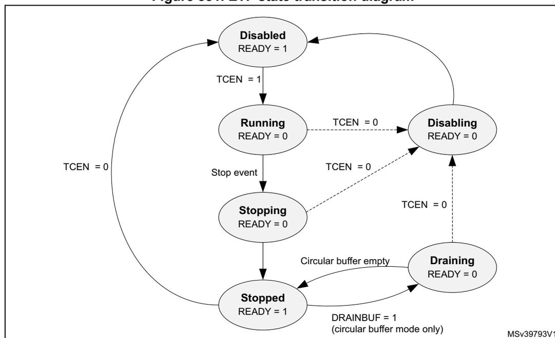
stateDiagram-v2
    [*] --> Disabled
    Disabled --> Running: TCEN = 1
    Running --> Stopping: Stop event
    Running --> Disabling: TCEN = 0
    Stopping --> Stopped
    Stopping --> Disabling: TCEN = 0
    Stopped --> Disabled: TCEN = 0
    Stopped --> Draining: DRAINBUF = 1 (circular buffer mode only)
    Draining --> Stopped: Circular buffer empty
    Disabling --> Disabled: TCEN = 0
    Disabling --> Draining: TCEN = 0
The diagram illustrates the state transitions for the ETF. It starts with an initial state pointing to 'Disabled' (READY = 1). From 'Disabled', a transition to 'Running' (READY = 0) occurs when TCEN = 1. From 'Running', a 'Stop event' leads to 'Stopping' (READY = 0), and setting TCEN = 0 leads to 'Disabling' (READY = 0). From 'Stopping', the state transitions to 'Stopped' (READY = 1) or to 'Disabling' (READY = 0) if TCEN = 0. From 'Stopped', setting TCEN = 0 returns the state to 'Disabled', and setting DRAINBUF = 1 (in circular buffer mode only) leads to 'Draining' (READY = 0). From 'Draining', the state returns to 'Stopped' when the circular buffer is empty. Finally, from 'Disabling', setting TCEN = 0 returns the state to 'Disabled', and setting TCEN = 0 also leads to 'Draining' (READY = 0). The diagram is labeled MSV39793V1.
For more information on the CoreSight™ trace memory controller component, refer to the Arm® CoreSight™ trace memory controller technical reference manual [3] .
ETF registers
ETF RAM size register (ETF_RSZ)
Address offset: 0x004
Reset value: 0x0000 0400
| 31 | 30 | 29 | 28 | 27 | 26 | 25 | 24 | 23 | 22 | 21 | 20 | 19 | 18 | 17 | 16 |
|---|---|---|---|---|---|---|---|---|---|---|---|---|---|---|---|
| Res. | RSZ[30:16] | ||||||||||||||
| r | r | r | r | r | r | r | r | r | r | r | r | r | r | r | |
| 15 | 14 | 13 | 12 | 11 | 10 | 9 | 8 | 7 | 6 | 5 | 4 | 3 | 2 | 1 | 0 |
| RSZ[15:0] | |||||||||||||||
| r | r | r | r | r | r | r | r | r | r | r | r | r | r | r | r |
Bit 31 Reserved, must be kept at reset value.
Bits 30:0 RSZ[30:0] : RAM size
The value of the field indicates the number of 32-bit words
0x400: 1024 words = 4 Kbytes
ETF status register (ETF_STS)
Address offset: 0x00C
Reset value: 0x0000 001C
| 31 | 30 | 29 | 28 | 27 | 26 | 25 | 24 | 23 | 22 | 21 | 20 | 19 | 18 | 17 | 16 |
|---|---|---|---|---|---|---|---|---|---|---|---|---|---|---|---|
| Res. | Res. | Res. | Res. | Res. | Res. | Res. | Res. | Res. | Res. | Res. | Res. | Res. | Res. | Res. | Res. |
| 15 | 14 | 13 | 12 | 11 | 10 | 9 | 8 | 7 | 6 | 5 | 4 | 3 | 2 | 1 | 0 |
| Res. | Res. | Res. | Res. | Res. | Res. | Res. | Res. | Res. | Res. | Res. | EMPTY | FTEMP TY | READY | TRIGD | FULL |
| r | r | r | r | r |
Bits 31:5 Reserved, must be kept at reset value.
Bit 4 EMPTY : Trace FIFO empty
This bit is valid only when the TCEN bit of the ETF_CTL register is high. This bit reads as zero when TCEN is low.
0: Trace FIFO contains data
1: Trace FIFO is empty.
Note: Empty trace FIFO does not mean that the ETF pipeline is empty. The latter is indicated by the FTEMPTY bit.
Bit 3 FTEMPTY : Formatter empty
This bit is set when trace capture has stopped, and all internal pipelines and buffers have been drained. Unlike READY, it is not affected by buffer drains. The ACQCOMP output reflects the value of this bit.
Bit 2 READY : ETF ready
This bit is set when trace capture has stopped and all internal pipelines and buffers have been drained (Stopped or Disabled state)
Bit 1 TRIGD : Triggered
The Triggered bit is set when trace capture is in progress and the TMC has detected a Trigger Event. This bit is cleared when leaving Disabled state.
This bit is operational only in the Circular buffer mode. In all other modes, this bit is always low.
This bit does not indicate that a trigger has been embedded in the formatted output trace data from the TMC. Trigger indication on the output trace stream is determined by the programming of the Formatter and Flush Control Register, ETF_FFCR.
Bit 0 FULL : Trace buffer full
In circular buffer mode, this flag is set when the RAM write pointer wraps around the top of the buffer, and remains set until the TCEN bit of the ETF_CTL register is cleared and set.
In software and hardware FIFO modes, this flag indicates that the current space in the trace memory is less than or equal to the value programmed in the ETF_BUFWM Register, that is, Fill level \( \geq \) MEM_SIZE - BUFWM.
This bit is cleared when leaving Disabled state. The FULL output reflects the value of this register bit.
ETF RAM read data register (ETF_RRD)
Address offset: 0x010
Reset value: Unknown
| 31 | 30 | 29 | 28 | 27 | 26 | 25 | 24 | 23 | 22 | 21 | 20 | 19 | 18 | 17 | 16 |
| RRD[31:16] | |||||||||||||||
| r | r | r | r | r | r | r | r | r | r | r | r | r | r | r | r |
| 15 | 14 | 13 | 12 | 11 | 10 | 9 | 8 | 7 | 6 | 5 | 4 | 3 | 2 | 1 | 0 |
| RRD[15:0] | |||||||||||||||
| r | r | r | r | r | r | r | r | r | r | r | r | r | r | r | r |
Bits 31:0 RRD[31:0] : RAM Read Data.
Circular buffer mode:
When in Stopped state and the buffer is not empty, reading this register returns the next word of data from the trace buffer. When the whole trace buffer has been read, the Empty bit in the ETF_STS Register is set, and subsequent reads return 0xFFFFFFFF. Reading this register when not in Stopped state returns 0xFFFFFFFF.
Software FIFO mode:
Reading this register returns data from the FIFO. If this register is read when the FIFO is empty, the data returned is 0xFFFFFFFF.
Hardware FIFO mode:
Reading this register returns 0xFFFFFFFF.
ETF RAM read pointer register (ETF_RRP)
Address offset: 0x014
Reset value: 0x0000 0000
| 31 | 30 | 29 | 28 | 27 | 26 | 25 | 24 | 23 | 22 | 21 | 20 | 19 | 18 | 17 | 16 |
|---|---|---|---|---|---|---|---|---|---|---|---|---|---|---|---|
| Res. | Res. | Res. | Res. | Res. | Res. | Res. | Res. | Res. | Res. | Res. | Res. | Res. | Res. | Res. | Res. |
| 15 | 14 | 13 | 12 | 11 | 10 | 9 | 8 | 7 | 6 | 5 | 4 | 3 | 2 | 1 | 0 |
| Res. | Res. | Res. | RRP[12:0] | ||||||||||||
| rw | rw | rw | rw | rw | rw | rw | rw | rw | rw | rw | rw | rw | |||
Bits 31:13 Reserved, must be kept at reset value.
Bits 12:0 RRP[12:0] : RAM Read Pointer
The RAM Read Pointer Register contains the value of the read pointer that is used to read entries from the trace memory over the APB interface via the ETF_RRD register. The pointer can be programmed with a byte address, 64-bit aligned (that is, bits 0 to 3 should be zero). The pointer is incremented by 8 each time a full 64-bit FIFO entry has been written. When the pointer reaches its maximum value, it wraps around.
This register can only be written to while in Disabled state. It can be read in Disabled state, in Stopped state in circular buffer mode and SW FIFO mode, and also in Running and Stopping states in SW FIFO mode.
ETF RAM write pointer register (ETF_RWP)
Address offset: 0x018
Reset value: 0x0000 0000
| 31 | 30 | 29 | 28 | 27 | 26 | 25 | 24 | 23 | 22 | 21 | 20 | 19 | 18 | 17 | 16 |
|---|---|---|---|---|---|---|---|---|---|---|---|---|---|---|---|
| Res. | Res. | Res. | Res. | Res. | Res. | Res. | Res. | Res. | Res. | Res. | Res. | Res. | Res. | Res. | Res. |
| 15 | 14 | 13 | 12 | 11 | 10 | 9 | 8 | 7 | 6 | 5 | 4 | 3 | 2 | 1 | 0 |
| Res. | Res. | Res. | RWP[12:0] | ||||||||||||
| rw | rw | rw | rw | rw | rw | rw | rw | rw | rw | rw | rw | rw | |||
Bits 31:13 Reserved, must be kept at reset value.
Bits 12:0 RWP[12:0] : RAM write pointer
The RAM write pointer register contains the value of the write pointer that is used to write entries into the trace memory over the APB interface via the ETF_RWD register. The pointer can be programmed with a byte address, 64-bit aligned (that is, bits 0 to 3 should be zero). The pointer is incremented by 8 each time a full 64-bit FIFO entry has been read. When the pointer reaches its maximum value, it wraps around.
This register can only be written to while in Disabled state. It can be read in Disabled state, in Stopped state in circular buffer mode and SW FIFO mode, and also in Running and Stopping states in SW FIFO mode.
ETF trigger counter register (ETF_TRG)
Address offset: 0x01C
Reset value: 0x0000 0000
| 31 | 30 | 29 | 28 | 27 | 26 | 25 | 24 | 23 | 22 | 21 | 20 | 19 | 18 | 17 | 16 |
|---|---|---|---|---|---|---|---|---|---|---|---|---|---|---|---|
| Res. | Res. | Res. | Res. | Res. | Res. | Res. | Res. | Res. | Res. | Res. | Res. | Res. | Res. | Res. | Res. |
| 15 | 14 | 13 | 12 | 11 | 10 | ||||||||||
| Res. | Res. | Res. | Res. | Res. | TRG[10:0] | ||||||||||
| rw | rw | rw | rw | rw | rw | rw | rw | rw | rw | rw | |||||
Bits 31:11 Reserved, must be kept at reset value.
Bits 10:0 TRG[10:0] : Trigger counter
In Circular buffer mode, specifies the number of 32-bit words to capture in the trace RAM following the detection of either a rising edge on the TRIGIN input or a trigger packet in the incoming trace stream, ATID =7'h7D. On capturing the specified number of data words, a trigger event occurs. The effect of a trigger event on the ETF behavior is controlled by the FFCR Register.
The number of 32-bit words written into the trace RAM following the trigger is the value stored in this register, plus one. This register is ignored when the ETF is in Software FIFO mode or Hardware FIFO mode. When the trigger counter starts counting, any additional triggers, either on TRIGIN or in the incoming trace stream, are ignored until the counter reaches zero. When the trigger counter has reached zero, it remains at zero until it is re-programmed with a write to this register.
This register is cleared when READY goes high, so that the state of the counter when trace capture has stopped does not affect a subsequent trace capture session. Writing to this register when not in Disabled state results in unpredictable behavior.
A read access to this register is permitted at any time when in Disabled state, or in Circular buffer mode. A read access returns the current value of the trigger counter.
ETF control register (ETF_CTL)
Address offset: 0x020
Reset value: 0x0000 0000
| 31 | 30 | 29 | 28 | 27 | 26 | 25 | 24 | 23 | 22 | 21 | 20 | 19 | 18 | 17 | 16 |
|---|---|---|---|---|---|---|---|---|---|---|---|---|---|---|---|
| Res. | Res. | Res. | Res. | Res. | Res. | Res. | Res. | Res. | Res. | Res. | Res. | Res. | Res. | Res. | Res. |
| 15 | 14 | 13 | 12 | 11 | 10 | 9 | 8 | 7 | 6 | 5 | 4 | 3 | 2 | 1 | 0 |
| Res. | Res. | Res. | Res. | Res. | Res. | Res. | Res. | Res. | Res. | Res. | Res. | Res. | Res. | Res. | TCEN |
| rw |
Bits 31:1 Reserved, must be kept at reset value.
Bit 0 TCEN : Trace capture enable
When writing:
0: Disable trace capture (moves from Running, Stopping or Stopped state into Disabling or Disabled state)
1: Enable trace capture (moves from Disabled state to Running state)
When reading, this bit is low when in Disabling or Disabled states, and high otherwise.
ETF RAM write data register (ETF_RWD)
Address offset: 0x024
Reset value: 0x0000 0000
| 31 | 30 | 29 | 28 | 27 | 26 | 25 | 24 | 23 | 22 | 21 | 20 | 19 | 18 | 17 | 16 |
|---|---|---|---|---|---|---|---|---|---|---|---|---|---|---|---|
| RWD[31:16] | |||||||||||||||
| w | w | w | w | w | w | w | w | w | w | w | w | w | w | w | w |
| 15 | 14 | 13 | 12 | 11 | 10 | 9 | 8 | 7 | 6 | 5 | 4 | 3 | 2 | 1 | 0 |
| RWD[15:0] | |||||||||||||||
| w | w | w | w | w | w | w | w | w | w | w | w | w | w | w | w |
Bits 31:0 RWD[31:0] : RAM write data
When in Disabled state, a write to this register stores data at the location pointed to by the RWP. Writes to this register when not in Disabled state are ignored. When a full memory width (64-bit) of data has been written, the data is written to memory and the RAM Write Pointer is incremented to the next memory word.
This register is used for test purposes.
ETF mode register (ETF_MODE)
Address offset: 0x028
Reset value: 0x0000 0000
| 31 | 30 | 29 | 28 | 27 | 26 | 25 | 24 | 23 | 22 | 21 | 20 | 19 | 18 | 17 | 16 |
|---|---|---|---|---|---|---|---|---|---|---|---|---|---|---|---|
| Res. | Res. | Res. | Res. | Res. | Res. | Res. | Res. | Res. | Res. | Res. | Res. | Res. | Res. | Res. | Res. |
| 15 | 14 | 13 | 12 | 11 | 10 | 9 | 8 | 7 | 6 | 5 | 4 | 3 | 2 | 1 | 0 |
| Res. | Res. | Res. | Res. | Res. | Res. | Res. | Res. | Res. | Res. | Res. | Res. | Res. | Res. | MODE[1:0] | |
| rw | rw | ||||||||||||||
Bits 31:2 Reserved, must be kept at reset value.
Bits 1:0 MODE[1:0] : Operation mode
- 00b: Circular buffer mode
In this mode, the trace memory is used as a circular buffer. Trace data is captured into the Trace memory starting from the location pointed to by the write pointer register. Even when the trace memory is full, incoming trace data continues to be overwritten into the trace memory until a stop condition has occurred.
- 01b: Software FIFO mode
In this mode, the trace memory is used as a FIFO that can be read through the RRD Register while trace is being captured. Trace data is captured into the trace RAM and when full, the incoming trace stream is stalled.
- 10b: Hardware FIFO mode
In this mode, the trace memory is used as a FIFO that is drained through the ATB master interface. Trace data is captured into the trace RAM and when full, the incoming trace stream is stalled. When the trace buffer is non-empty, trace data is drained out through the ATB master interface to the TPIU.
- 11b: Reserved
ETF latched buffer fill level register (ETF_LBUFLVL)
Address offset: 0x02C
Reset value: 0x0000 0000
| 31 | 30 | 29 | 28 | 27 | 26 | 25 | 24 | 23 | 22 | 21 | 20 | 19 | 18 | 17 | 16 |
|---|---|---|---|---|---|---|---|---|---|---|---|---|---|---|---|
| Res. | Res. | Res. | Res. | Res. | Res. | Res. | Res. | Res. | Res. | Res. | Res. | Res. | Res. | Res. | Res. |
| 15 | 14 | 13 | 12 | 11 | 10 | 9 | 8 | 7 | 6 | 5 | 4 | 3 | 2 | 1 | 0 |
| Res. | Res. | Res. | Res. | LBUFLEVEL[11:0] | |||||||||||
| r | r | r | r | r | r | r | r | r | r | r | r | ||||
Bits 31:12 Reserved, must be kept at reset value.
Bits 11:0 LBUFLEVEL[11:0] : Latched buffer fill level
Reading this register returns the maximum fill level of the trace memory in 32-bit words since this register was last read. Reading this register also results in its contents being updated to the current fill level.
When entering Disabled state, this register retains its last value. While in Disabled state, reads from this register do not affect its value. When exiting Disabled state, the LBUFLEVEL register is cleared.
This register is used for performance analysis of the trace system.
ETF current buffer fill level register (ETF_CBUFLVL)
Address offset: 0x030
Reset value: 0x0000 0000
| 31 | 30 | 29 | 28 | 27 | 26 | 25 | 24 | 23 | 22 | 21 | 20 | 19 | 18 | 17 | 16 |
|---|---|---|---|---|---|---|---|---|---|---|---|---|---|---|---|
| Res. | Res. | Res. | Res. | Res. | Res. | Res. | Res. | Res. | Res. | Res. | Res. | Res. | Res. | Res. | Res. |
| 15 | 14 | 13 | 12 | 11 | 10 | 9 | 8 | 7 | 6 | 5 | 4 | 3 | 2 | 1 | 0 |
|---|---|---|---|---|---|---|---|---|---|---|---|---|---|---|---|
| Res. | Res. | Res. | Res. | CBUFLEVEL[11:0] | |||||||||||
| r | r | r | r | r | r | r | r | r | r | r | r | ||||
Bits 31:12 Reserved, must be kept at reset value.
Bits 11:0 CBUFLEVEL[11:0] : Current buffer fill level
Reading this register returns the current fill level of the trace memory in 32-bit words.
This register is cleared when TCEN is low.
ETF buffer level watermark register (ETF_BUFWM)
Address offset: 0x034
Reset value: 0x0000 0000
| 31 | 30 | 29 | 28 | 27 | 26 | 25 | 24 | 23 | 22 | 21 | 20 | 19 | 18 | 17 | 16 |
|---|---|---|---|---|---|---|---|---|---|---|---|---|---|---|---|
| Res. | Res. | Res. | Res. | Res. | Res. | Res. | Res. | Res. | Res. | Res. | Res. | Res. | Res. | Res. | Res. |
| 15 | 14 | 13 | 12 | 11 | 10 | 9 | 8 | 7 | 6 | 5 | 4 | 3 | 2 | 1 | 0 |
| Res. | Res. | Res. | Res | Res | BUFWM[10:0] | ||||||||||
| rw | rw | rw | rw | rw | rw | rw | rw | rw | rw | rw | |||||
Bits 31:11 Reserved, must be kept at reset value.
Bits 10:0 BUFWM[10:0] : Buffer level watermark
The value programmed into this register indicates the required threshold vacancy level in the trace memory in 32-bit words. When the space in the FIFO is less than or equal to this value, that is, Fill level \( \geq \) MEM_SIZE - BUFWM, the FULL output is pulled high and the FULL bit in the STS Register is set.
This register is used only in Software FIFO and Hardware FIFO modes. In Circular buffer mode, this functionality can be obtained by programming the RWP to the required vacancy trigger level, so that when the pointer wraps around, the FULL bit is set indicating that the vacancy level has fallen below the required level.
The maximum value that can be written into this register is MEM_SIZE - 1. In this case, the FULL bit output is asserted after the first 32-bit word is written to trace memory.
Writing to this register other than when in disabled state results in unpredictable behavior.
ETF formatter and flush status register (ETF_FFSR)
Address offset: 0x300
Reset value: 0x0000 0002
| 31 | 30 | 29 | 28 | 27 | 26 | 25 | 24 | 23 | 22 | 21 | 20 | 19 | 18 | 17 | 16 |
|---|---|---|---|---|---|---|---|---|---|---|---|---|---|---|---|
| Res. | Res. | Res. | Res. | Res. | Res. | Res. | Res. | Res. | Res. | Res. | Res. | Res. | Res. | Res. | Res. |
| 15 | 14 | 13 | 12 | 11 | 10 | 9 | 8 | 7 | 6 | 5 | 4 | 3 | 2 | 1 | 0 |
| Res. | Res. | Res. | Res. | Res. | Res. | Res. | Res. | Res. | Res. | Res. | Res. | Res. | Res. | FTSTOPPED | FLINPROG |
| r | r | ||||||||||||||
Bits 31:2 Reserved, must be kept at reset value.
Bit 1 FTSTOPPED : Formatter stopped
This bit behaves in the same way as the FTEMPTY bit in the ETF_STS register.
Bit 0 FLINPROG : Flush in progress
Indicates whether a flush on the ATB slave port is in progress. This bit reflects the status of the AFVALIDS output. A flush can be initiated by the flush control bits in the ETF_FFCR register, or requested by the ATB master port.
0: No flush in progress
1: Flush in progress
ETF formatter and flush control register (ETF_FFCR)
Address offset: 0x304
Reset value: 0x0000 0000
| 31 | 30 | 29 | 28 | 27 | 26 | 25 | 24 | 23 | 22 | 21 | 20 | 19 | 18 | 17 | 16 |
|---|---|---|---|---|---|---|---|---|---|---|---|---|---|---|---|
| Res. | Res. | Res. | Res. | Res. | Res. | Res. | Res. | Res. | Res. | Res. | Res. | Res. | Res. | Res. | Res. |
| 15 | 14 | 13 | 12 | 11 | 10 | 9 | 8 | 7 | 6 | 5 | 4 | 3 | 2 | 1 | 0 |
| Res. | DRAIN BUF. | STOP NTRG EV. | STOP ONFL | Res. | TRIGO NFL. | TRGON TRGEV | TRGON TRGIN | Res. | FLUSH MAN | FONTR GEV. | FONFLI N | Res. | Res. | ENTI | ENFT |
| rw | rw | rw | rw | rw | rw | rw | rw | rw | rw | rw |
Bits 31:15 Reserved, must be kept at reset value.
Bit 14 DRAINBUF : Drain buffer
This bit is used to enable draining of the trace data through the ATB master interface after the formatter has stopped. This is useful in Circular buffer mode to capture trace data into trace memory and then to drain the captured trace through the ATB master interface.
Writing a one to this bit when in Stopped state starts the drain of the trace buffer content through the ATB Master interface. This bit always reads as zero. The READY bit in the ETF_STS register goes low while the drain is in progress.
This bit is only functional when the ETF is in Circular buffer mode and formatting is enabled, that is, the ENFT bit in the ETF_FFCR register is set. Setting this bit when the ETF is in any other mode, or when not in Stopped state, results in Unpredictable behavior.
When trace capture is complete in Circular buffer mode, all of the captured trace must be retrieved from the trace memory through the same mechanism, either read all trace data out through RRD reads, or drain all trace data by setting the DRAINBUF bit. Setting the DRAINBUF bit after some of the captured trace has been read out through RRD results in unpredictable behavior.
Bit 13 STPONTRGEV : Stop on trigger event
0: No effect
1: Stop trace capture when a trigger event occurs
Enabling the ETF in Software FIFO mode or Hardware FIFO mode with this bit set results in unpredictable behavior.
Bit 12 STOPONFL : Stop on flush
0: No effect
1: Stop trace capture when flush is completed
If a flush is initiated by the ATB master interface, its completion does not lead to a formatter stop regardless of the value programmed in this bit.
Bit 11 Reserved, must be kept at reset value.
Bit 10 TRIGONFL : Trigger on flush
0: No effect
1: Indicate a trigger in the trace stream when flush is completed
If ENFT and ENTI are both clear, this bit is ignored and no trigger is inserted into the trace stream.
If a flush is initiated by the ATB master interface, its completion does not lead to a trigger indication regardless of the value programmed in this bit.
Bit 9 TRGONTRGEV : Trigger on trigger event
0: No effect
1: Indicate a trigger in the trace stream when trigger event occurs
If ENFT and ENTI are both clear, this bit is ignored and no trigger is inserted into the trace stream.
This bit is not supported in Software FIFO mode or Hardware FIFO mode.
Bit 8 TRGONTRGIN : Trigger on trigger in
0: No effect
1: Indicate a trigger in the trace stream when a rising edge is detected on the TRIGIN input.
If ENFT and ENTI are both clear, this bit is ignored and no trigger is inserted into the trace stream.
Bit 7 Reserved, must be kept at reset value.
Bit 6 FLUSHMAN : Manual flush
0: No effect
1: Flush the trace FIFO and pipeline
This bit is cleared automatically when the flush completes. If the TCEN bit in the ETF_CTL register is 0, writes to this bit are ignored.
Bit 5 FONTRGEV : Flush on trigger event
0: No effect
1: Flush the trace FIFO and pipeline if a trigger event occurs
This bit is not supported in Software FIFO mode or Hardware FIFO mode. If STOPONTRGEV is set, this bit is ignored.
Bit 4 FONFLIN : Flush on flush in
0: No effect
1: Flush the trace FIFO and pipeline if when a rising edge is detected on the FLUSHIN input
Bits 3:2 Reserved, must be kept at reset value.
Bit 1 ENTI : Enable trigger insertion
Setting this bit enables the insertion of triggers in the formatted trace stream. A trigger is flagged by inserting one byte of data 8'h00 with ATID 7'h7D in the trace stream. Trigger indication on the trace stream is further controlled by the register bits TRIGONFL, TRGONTRGEV, and TRGONTRGIN in the FFCR Register. This bit can only be changed when READY is high, and TCEN is low. This bit takes effect only when the ENFT register bit in this register is set. If ENTI bit is set to high when ENFT is low, it results in formatting being enabled.
Bit 0 ENFT : Enable formatting.
0: Formatting is disabled. Incoming trace data is assumed to be from a single trace source.
1: Formatting is enabled.
If multiple ATIDs are received by the ETF when trace capture is enabled and the formatter is disabled, an interleaving of trace data occurs. Disabling of formatting is supported only in Circular buffer mode. If the ETF is enabled in a mode other than Circular buffer mode with ENFT low, then formatting is enabled. If ENTI bit is set to high when ENFT is low, it results in formatting being enabled.
This bit is ignored when in Disabled state.
ETF periodic synchronization counter register (ETF_PSCR)
Address offset: 0x308
Reset value: 0x0000 000A
| 31 | 30 | 29 | 28 | 27 | 26 | 25 | 24 | 23 | 22 | 21 | 20 | 19 | 18 | 17 | 16 |
|---|---|---|---|---|---|---|---|---|---|---|---|---|---|---|---|
| Res. | Res. | Res. | Res. | Res. | Res. | Res. | Res. | Res. | Res. | Res. | Res. | Res. | Res. | Res. | Res. |
| 15 | 14 | 13 | 12 | 11 | 10 | 9 | 8 | 7 | 6 | 5 | 4 | 3 | 2 | 1 | 0 |
| Res. | Res. | Res. | Res. | Res. | Res. | Res. | Res. | Res. | Res. | Res. | PSCOUNT[4:0] | ||||
| rw | rw | rw | rw | rw | |||||||||||
Bits 31:5 Reserved, must be kept at reset value.
Bits 4:0 PSCOUNT[4:0] : Synchronization counter reload value
Determines the reload value of the Synchronization Counter. The reload value takes effect the next time the counter reaches zero. Reads from this register return the reload value programmed into this register. This register is set to 0xA on reset, corresponding to a synchronization period of 1024 bytes.
0x0: Synchronization disabled
0x1-0x6: Reserved
0x7-0x1B: Synchronization period is \( 2^{\text{PSCOUNT}} \) bytes
0x1C-0x1F: Reserved
ETF claim tag set register (ETF_CLAIMSET)Address offset: 0xFA0
Reset value: 0x0000 000F
| 31 | 30 | 29 | 28 | 27 | 26 | 25 | 24 | 23 | 22 | 21 | 20 | 19 | 18 | 17 | 16 |
|---|---|---|---|---|---|---|---|---|---|---|---|---|---|---|---|
| Res. | Res. | Res. | Res. | Res. | Res. | Res. | Res. | Res. | Res. | Res. | Res. | Res. | Res. | Res. | Res. |
| 15 | 14 | 13 | 12 | 11 | 10 | 9 | 8 | 7 | 6 | 5 | 4 | 3 | 2 | 1 | 0 |
| Res. | Res. | Res. | Res. | Res. | Res. | Res. | Res. | Res. | Res. | Res. | Res. | CLAIMSET[3:0] | |||
| rw | rw | rw | rw | ||||||||||||
Bits 31:4 Reserved, must be kept at reset value.
Bits 3:0 CLAIMSET[3:0] : Set claim tag bitsWrite:
0000: No effect
xxx1: Set bit 0
xx1x: Set bit 1
x1xx: Set bit 2
1xxx: Set bit 3
Read:
0xF: Indicates there are four bits in claim tag
ETF claim tag clear register (ETF_CLAIMCLR)Address offset: 0xFA4
Reset value: 0x0000 0000
| 31 | 30 | 29 | 28 | 27 | 26 | 25 | 24 | 23 | 22 | 21 | 20 | 19 | 18 | 17 | 16 |
|---|---|---|---|---|---|---|---|---|---|---|---|---|---|---|---|
| Res. | Res. | Res. | Res. | Res. | Res. | Res. | Res. | Res. | Res. | Res. | Res. | Res. | Res. | Res. | Res. |
| 15 | 14 | 13 | 12 | 11 | 10 | 9 | 8 | 7 | 6 | 5 | 4 | 3 | 2 | 1 | 0 |
| Res. | Res. | Res. | Res. | Res. | Res. | Res. | Res. | Res. | Res. | Res. | Res. | CLAIMCLR[3:0] | |||
Bits 31:4 Reserved, must be kept at reset value.
Bits 3:0 CLAIMCLR[3:0] : Reset claim tag bitsWrite:
0000: No effect
xxx1: Clear bit 0
xx1x: Clear bit 1
x1xx: Clear bit 2
1xxx: Clear bit 3
Read: Returns current value of claim tag
ETF lock access register (ETF_LAR)
Address offset: 0xFB0
Reset value: N/A
| 31 | 30 | 29 | 28 | 27 | 26 | 25 | 24 | 23 | 22 | 21 | 20 | 19 | 18 | 17 | 16 |
| ACCESS_W[31:16] | |||||||||||||||
| w | w | w | w | w | w | w | w | w | w | w | w | w | w | w | w |
| 15 | 14 | 13 | 12 | 11 | 10 | 9 | 8 | 7 | 6 | 5 | 4 | 3 | 2 | 1 | 0 |
| ACCESS_W[15:0] | |||||||||||||||
| w | w | w | w | w | w | w | w | w | w | w | w | w | w | w | w |
Bits 31:0 ACCESS_W[31:0] : ETF register access enable
Enables write access to some ETF registers by processor cores (debuggers do not need to unlock the component)
0xC5ACCE55: Enable write access
Other values: Disable write access
ETF lock status register (ETF_LSR)
Address offset: 0xFB4
Reset value: 0x0000 0003
| 31 | 30 | 29 | 28 | 27 | 26 | 25 | 24 | 23 | 22 | 21 | 20 | 19 | 18 | 17 | 16 |
| Res. | Res. | Res. | Res. | Res. | Res. | Res. | Res. | Res. | Res. | Res. | Res. | Res. | Res. | Res. | Res. |
| 15 | 14 | 13 | 12 | 11 | 10 | 9 | 8 | 7 | 6 | 5 | 4 | 3 | 2 | 1 | 0 |
| Res. | Res. | Res. | Res. | Res. | Res. | Res. | Res. | Res. | Res. | Res. | Res. | Res. | LOCK TYPE | LOCK GRANT | LOCK EXIST |
| r | r | r |
Bits 31:3 Reserved, must be kept at reset value.
Bit 2 LOCKTYPE : Size of the ETF_LAR register
0: 32-bit
Bit 1 LOCKGRANT : Current status of lock
This bit always returns zero when read by an external debugger.
0: Write access is permitted
1: Write access is blocked. Only read access is permitted.
Bit 0 LOCKEXIST : Existence of lock control mechanism
The bit indicates whether a lock control mechanism exists. It always returns zero when read by an external debugger.
0: No lock control mechanism exists
1: Lock control mechanism is implemented
ETF authentication status register (ETF_AUTHSTAT)Address offset: 0xFB8
Reset value: 0x0000 0000
| 31 | 30 | 29 | 28 | 27 | 26 | 25 | 24 | 23 | 22 | 21 | 20 | 19 | 18 | 17 | 16 |
|---|---|---|---|---|---|---|---|---|---|---|---|---|---|---|---|
| Res. | Res. | Res. | Res. | Res. | Res. | Res. | Res. | Res. | Res. | Res. | Res. | Res. | Res. | Res. | Res. |
| 15 | 14 | 13 | 12 | 11 | 10 | 9 | 8 | 7 | 6 | 5 | 4 | 3 | 2 | 1 | 0 |
| Res. | Res. | Res. | Res. | Res. | Res. | Res. | Res. | SNID[1:0] | SID[1:0] | NSNID[1:0] | NSID[1:0] | ||||
| r | r | r | r | r | r | r | r |
Bits 31:8 Reserved, must be kept at reset value.
Bits 7:6 SNID[1:0] : Security level for secure non-invasive debug0x0: Not implemented
Bits 5:4 SID[1:0] : Security level for secure invasive debug0x0: Not implemented
Bits 3:2 NSNID[1:0] : Security level for non-secure non-invasive debug0x0: Not implemented
Bits 1:0 NSID[1:0] : Security level for non-secure invasive debug0x0: Not implemented
ETF device configuration register (ETF_DEVID)Address offset: 0xFC8
Reset value: 0x0000 01C0
| 31 | 30 | 29 | 28 | 27 | 26 | 25 | 24 | 23 | 22 | 21 | 20 | 19 | 18 | 17 | 16 |
|---|---|---|---|---|---|---|---|---|---|---|---|---|---|---|---|
| Res. | Res. | Res. | Res. | Res. | Res. | Res. | Res. | Res. | Res. | Res. | Res. | Res. | Res. | Res. | Res. |
| 15 | 14 | 13 | 12 | 11 | 10 | 9 | 8 | 7 | 6 | 5 | 4 | 3 | 2 | 1 | 0 |
| Res. | Res. | Res. | Res. | Res. | MEMWIDTH[2:0] | CONFIGTYP[1:0] | CLK SCHEM | ATBINPORTCNT[4:0] | |||||||
| r | r | r | r | r | r | r | r | r | r | r | |||||
Bits 31:11 Reserved, must be kept at reset value.
Bits 10:8 MEMWIDTH[2:0] : Memory interface data bus width0x3: 64 bits (corresponds to 32-bit ATB data)
Bits 7:6 CONFIGTYP[1:0] : Configuration type of component (ETB, ETR or ETF)0x2: ETF
Bit 5 CLKSCHEM : RAM clocking scheme (synchronous or asynchronous)0: Synchronous
Bits 4:0 ATBINPORTCNT[4:0] : Number/type of ATB input port multiplexing0x0: None
ETF device type identifier register (ETF_DEVTYPE)
Address offset: 0xFCC
Reset value: 0x0000 0032
| 31 | 30 | 29 | 28 | 27 | 26 | 25 | 24 | 23 | 22 | 21 | 20 | 19 | 18 | 17 | 16 |
|---|---|---|---|---|---|---|---|---|---|---|---|---|---|---|---|
| Res. | Res. | Res. | Res. | Res. | Res. | Res. | Res. | Res. | Res. | Res. | Res. | Res. | Res. | Res. | Res. |
| 15 | 14 | 13 | 12 | 11 | 10 | 9 | 8 | 7 | 6 | 5 | 4 | 3 | 2 | 1 | 0 |
| Res. | Res. | Res. | Res. | Res. | Res. | Res. | Res. | SUBTYPE[3:0] | MAJORTYPE[3:0] | ||||||
| r | r | r | r | r | r | r | r | ||||||||
Bits 31:8 Reserved, must be kept at reset value.
Bits 7:4 SUBTYPE[3:0] : Sub-classification
0x3: Captures trace data from the ATB slave interface into RAM that can be drained through the ATB master interface
Bits 3:0 MAJORTYPE[3:0] : Major classification
0x2: Component is a trace link because it has an ATB master interface through which trace data can be drained out in Hardware FIFO mode.
ETF CoreSight peripheral identity register 4 (ETF_PIDR4)
Address offset: 0xFD0
Reset value: 0x0000 0004
| 31 | 30 | 29 | 28 | 27 | 26 | 25 | 24 | 23 | 22 | 21 | 20 | 19 | 18 | 17 | 16 |
|---|---|---|---|---|---|---|---|---|---|---|---|---|---|---|---|
| Res. | Res. | Res. | Res. | Res. | Res. | Res. | Res. | Res. | Res. | Res. | Res. | Res. | Res. | Res. | Res. |
| 15 | 14 | 13 | 12 | 11 | 10 | 9 | 8 | 7 | 6 | 5 | 4 | 3 | 2 | 1 | 0 |
| Res. | Res. | Res. | Res. | Res. | Res. | Res. | Res. | 4KCOUNT[3:0] | JEP106CON[3:0] | ||||||
| r | r | r | r | r | r | r | r | ||||||||
Bits 31:8 Reserved, must be kept at reset value.
Bits 7:4 4KCOUNT[3:0] : Register file size
0x0: Register file occupies a single 4 Kbyte region
Bits 3:0 JEP106CON[3:0] : JEP106 continuation code
0x4: Arm® JEDEC code
ETF CoreSight peripheral identity register 0 (ETF_PIDR0)Address offset: 0xFE0
Reset value: 0x0000 0061
| 31 | 30 | 29 | 28 | 27 | 26 | 25 | 24 | 23 | 22 | 21 | 20 | 19 | 18 | 17 | 16 |
|---|---|---|---|---|---|---|---|---|---|---|---|---|---|---|---|
| Res. | Res. | Res. | Res. | Res. | Res. | Res. | Res. | Res. | Res. | Res. | Res. | Res. | Res. | Res. | Res. |
| 15 | 14 | 13 | 12 | 11 | 10 | 9 | 8 | 7 | 6 | 5 | 4 | 3 | 2 | 1 | 0 |
| Res. | Res. | Res. | Res. | Res. | Res. | Res. | Res. | PARTNUM[7:0] | |||||||
| r | r | r | r | r | r | r | r | ||||||||
Bits 31:8 Reserved, must be kept at reset value.
Bits 7:0 PARTNUM[7:0] : Part number field, bits [7:0]0x61: ETF part number
ETF CoreSight peripheral identity register 1 (ETF_PIDR1)Address offset: 0xFE4
Reset value: 0x0000 00B9
| 31 | 30 | 29 | 28 | 27 | 26 | 25 | 24 | 23 | 22 | 21 | 20 | 19 | 18 | 17 | 16 |
|---|---|---|---|---|---|---|---|---|---|---|---|---|---|---|---|
| Res. | Res. | Res. | Res. | Res. | Res. | Res. | Res. | Res. | Res. | Res. | Res. | Res. | Res. | Res. | Res. |
| 15 | 14 | 13 | 12 | 11 | 10 | 9 | 8 | 7 | 6 | 5 | 4 | 3 | 2 | 1 | 0 |
| Res. | Res. | Res. | Res. | Res. | Res. | Res. | Res. | JEP106ID[3:0] | PARTNUM[11:8] | ||||||
| r | r | r | r | r | r | r | r | ||||||||
Bits 31:8 Reserved, must be kept at reset value.
Bits 7:4 JEP106ID[3:0] : JEP106 identity code field, bits [3:0]0xB: Arm® JEDEC code
Bits 3:0 PARTNUM[11:8] : Part number field, bits [11:8]0x9: ETF part number
ETF CoreSight peripheral identity register 2 (ETF_PIDR2)Address offset: 0xFE8
Reset value: 0x0000 001B
| 31 | 30 | 29 | 28 | 27 | 26 | 25 | 24 | 23 | 22 | 21 | 20 | 19 | 18 | 17 | 16 |
|---|---|---|---|---|---|---|---|---|---|---|---|---|---|---|---|
| Res. | Res. | Res. | Res. | Res. | Res. | Res. | Res. | Res. | Res. | Res. | Res. | Res. | Res. | Res. | Res. |
| 15 | 14 | 13 | 12 | 11 | 10 | 9 | 8 | 7 | 6 | 5 | 4 | 3 | 2 | 1 | 0 |
| Res. | Res. | Res. | Res. | Res. | Res. | Res. | Res. | REVISION[3:0] | JEDEC | JEP106ID[6:4] | |||||
| r | r | r | r | r | r | r | r | ||||||||
Bits 31:8 Reserved, must be kept at reset value.
Bits 7:4 REVISION[3:0] : Component revision number
0x1: r0p1
Bit 3 JEDEC : JEDEC assigned value
1: Designer ID specified by JEDEC
Bits 2:0 JEP106ID[6:4] : JEP106 identity code field, bits [6:4]
0x3: Arm® JEDEC code
ETF CoreSight peripheral identity register 3 (ETF_PIDR3)
Address offset: 0xFEC
Reset value: 0x0000 0000
| 31 | 30 | 29 | 28 | 27 | 26 | 25 | 24 | 23 | 22 | 21 | 20 | 19 | 18 | 17 | 16 |
|---|---|---|---|---|---|---|---|---|---|---|---|---|---|---|---|
| Res. | Res. | Res. | Res. | Res. | Res. | Res. | Res. | Res. | Res. | Res. | Res. | Res. | Res. | Res. | Res. |
| 15 | 14 | 13 | 12 | 11 | 10 | 9 | 8 | 7 | 6 | 5 | 4 | 3 | 2 | 1 | 0 |
| Res. | Res. | Res. | Res. | Res. | Res. | Res. | Res. | REVAND[3:0] | CMOD[3:0] | ||||||
| r | r | r | r | r | r | r | r | ||||||||
Bits 31:8 Reserved, must be kept at reset value.
Bits 7:4 REVAND[3:0] : Metal fix version
0x0: No metal fix
Bits 3:0 CMOD[3:0] : Customer modified
0x0: No customer modifications
ETF CoreSight component identity register 0 (ETF_CIDR0)
Address offset: 0xFF0
Reset value: 0x0000 000D
| 31 | 30 | 29 | 28 | 27 | 26 | 25 | 24 | 23 | 22 | 21 | 20 | 19 | 18 | 17 | 16 |
|---|---|---|---|---|---|---|---|---|---|---|---|---|---|---|---|
| Res. | Res. | Res. | Res. | Res. | Res. | Res. | Res. | Res. | Res. | Res. | Res. | Res. | Res. | Res. | Res. |
| 15 | 14 | 13 | 12 | 11 | 10 | 9 | 8 | 7 | 6 | 5 | 4 | 3 | 2 | 1 | 0 |
| Res. | Res. | Res. | Res. | Res. | Res. | Res. | Res. | PREAMBLE[7:0] | |||||||
| r | r | r | r | r | r | r | r | ||||||||
Bits 31:8 Reserved, must be kept at reset value.
Bits 7:0 PREAMBLE[7:0] : Component ID field, bits [7:0]
0x0D: Common ID value
ETF CoreSight component identity register 1 (ETF_CIDR1)
Address offset: 0xFF4
Reset value: 0x0000 0090
| 31 | 30 | 29 | 28 | 27 | 26 | 25 | 24 | 23 | 22 | 21 | 20 | 19 | 18 | 17 | 16 |
|---|---|---|---|---|---|---|---|---|---|---|---|---|---|---|---|
| Res. | Res. | Res. | Res. | Res. | Res. | Res. | Res. | Res. | Res. | Res. | Res. | Res. | Res. | Res. | Res. |
| 15 | 14 | 13 | 12 | 11 | 10 | 9 | 8 | 7 | 6 | 5 | 4 | 3 | 2 | 1 | 0 |
| Res. | Res. | Res. | Res. | Res. | Res. | Res. | Res. | ||||||||
| CLASS[3:0] | PREAMBLE[11:8] | ||||||||||||||
| r | r | r | r | r | r | r | r | ||||||||
Bits 31:8 Reserved, must be kept at reset value.
Bits 7:4 CLASS[3:0] : Component ID field, bits [15:12] - component class
0x9: CoreSight component
Bits 3:0 PREAMBLE[11:8] : Component ID field, bits [11:8]
0x0: Common ID value
ETF CoreSight component identity register 2 (ETF_CIDR2)
Address offset: 0xFF8
Reset value: 0x0000 0005
| 31 | 30 | 29 | 28 | 27 | 26 | 25 | 24 | 23 | 22 | 21 | 20 | 19 | 18 | 17 | 16 |
|---|---|---|---|---|---|---|---|---|---|---|---|---|---|---|---|
| Res. | Res. | Res. | Res. | Res. | Res. | Res. | Res. | Res. | Res. | Res. | Res. | Res. | Res. | Res. | Res. |
| 15 | 14 | 13 | 12 | 11 | 10 | 9 | 8 | 7 | 6 | 5 | 4 | 3 | 2 | 1 | 0 |
| Res. | Res. | Res. | Res. | Res. | Res. | Res. | Res. | ||||||||
| PREAMBLE[19:12] | |||||||||||||||
| r | r | r | r | r | r | r | r | ||||||||
Bits 31:8 Reserved, must be kept at reset value.
Bits 7:0 PREAMBLE[19:12] : Component ID field, bits [23:16]
0x05: Common ID value
ETF CoreSight component identity register 3 (ETF_CIDR3)
Address offset: 0xFFC
Reset value: 0x0000 00B1
| 31 | 30 | 29 | 28 | 27 | 26 | 25 | 24 | 23 | 22 | 21 | 20 | 19 | 18 | 17 | 16 |
|---|---|---|---|---|---|---|---|---|---|---|---|---|---|---|---|
| Res. | Res. | Res. | Res. | Res. | Res. | Res. | Res. | Res. | Res. | Res. | Res. | Res. | Res. | Res. | Res. |
| 15 | 14 | 13 | 12 | 11 | 10 | 9 | 8 | 7 | 6 | 5 | 4 | 3 | 2 | 1 | 0 |
| Res. | Res. | Res. | Res. | Res. | Res. | Res. | Res. | ||||||||
| PREAMBLE[27:20] | |||||||||||||||
| r | r | r | r | r | r | r | r | ||||||||
Bits 31:8 Reserved, must be kept at reset value.
Bits 7:0
PREAMBLE[27:20]
: Component ID field, bits [31:24]
0xB1: Common ID value
ETF register map and reset values
Table 638. ETF register map and reset values
| Offset | Register name | 31 | 30 | 29 | 28 | 27 | 26 | 25 | 24 | 23 | 22 | 21 | 20 | 19 | 18 | 17 | 16 | 15 | 14 | 13 | 12 | 11 | 10 | 9 | 8 | 7 | 6 | 5 | 4 | 3 | 2 | 1 | 0 | |
|---|---|---|---|---|---|---|---|---|---|---|---|---|---|---|---|---|---|---|---|---|---|---|---|---|---|---|---|---|---|---|---|---|---|---|
| 0x004 | ETF_RSZ | Res. | RSZ[30:0] | |||||||||||||||||||||||||||||||
| Reset value | 0 | 0 | 0 | 0 | 0 | 0 | 0 | 0 | 0 | 0 | 0 | 0 | 0 | 0 | 0 | 0 | 0 | 0 | 0 | 1 | 0 | 0 | 0 | 0 | 0 | 0 | 0 | 0 | 0 | 0 | 0 | |||
| 0x008 | Reserved | Reserved | ||||||||||||||||||||||||||||||||
| 0x00C | ETF_STS | Res. | Res. | Res. | Res. | Res. | Res. | Res. | Res. | Res. | Res. | Res. | Res. | Res. | Res. | Res. | Res. | Res. | Res. | Res. | Res. | Res. | Res. | Res. | Res. | Res. | Res. | Res. | Res. | EMPTY | FTEEMPTY | READY | TRIGD | FULL |
| Reset value | 1 | 1 | 1 | 0 | 0 | |||||||||||||||||||||||||||||
| 0x010 | ETF_RRD | RRD[31:0] | ||||||||||||||||||||||||||||||||
| Reset value | - | - | - | - | - | - | - | - | - | - | - | - | - | - | - | - | - | - | - | - | - | - | - | - | - | - | - | - | - | - | - | - | ||
| 0x014 | ETF_RRP | Res. | Res. | Res. | Res. | Res. | Res. | Res. | Res. | Res. | Res. | Res. | Res. | Res. | Res. | Res. | Res. | Res. | Res. | Res. | RRP[12:0] | |||||||||||||
| Reset value | 0 | 0 | 0 | 0 | 0 | 0 | 0 | 0 | 0 | 0 | 0 | 0 | 0 | |||||||||||||||||||||
| 0x018 | ETF_RWP | Res. | Res. | Res. | Res. | Res. | Res. | Res. | Res. | Res. | Res. | Res. | Res. | Res. | Res. | Res. | Res. | Res. | Res. | Res. | RWP[12:0] | |||||||||||||
| Reset value | 0 | 0 | 0 | 0 | 0 | 0 | 0 | 0 | 0 | 0 | 0 | 0 | 0 | |||||||||||||||||||||
| 0x01C | ETF_TRG | Res. | Res. | Res. | Res. | Res. | Res. | Res. | Res. | Res. | Res. | Res. | Res. | Res. | Res. | Res. | Res. | Res. | Res. | Res. | Res. | Res. | TRG[10:0] | |||||||||||
| Reset value | 0 | 0 | 0 | 0 | 0 | 0 | 0 | 0 | 0 | 0 | 0 | |||||||||||||||||||||||
| 0x020 | ETF_CTL | Res. | Res. | Res. | Res. | Res. | Res. | Res. | Res. | Res. | Res. | Res. | Res. | Res. | Res. | Res. | Res. | Res. | Res. | Res. | Res. | Res. | Res. | Res. | Res. | Res. | Res. | Res. | Res. | Res. | Res. | Res. | TCEN | |
| Reset value | 0 | |||||||||||||||||||||||||||||||||
| 0x024 | ETF_RWD | RWD[31:0] | ||||||||||||||||||||||||||||||||
| Reset value | - | - | - | - | - | - | - | - | - | - | - | - | - | - | - | - | - | - | - | - | - | - | - | - | - | - | - | - | - | - | - | - | ||
| 0x028 | ETF_MODE | Res. | Res. | Res. | Res. | Res. | Res. | Res. | Res. | Res. | Res. | Res. | Res. | Res. | Res. | Res. | Res. | Res. | Res. | Res. | Res. | Res. | Res. | Res. | Res. | Res. | Res. | Res. | Res. | Res. | Res. | MODE[1:0] | ||
| Reset value | 0 | 0 | ||||||||||||||||||||||||||||||||
| 0x02C | ETF_LBUFLVL | Res. | Res. | Res. | Res. | Res. | Res. | Res. | Res. | Res. | Res. | Res. | Res. | Res. | Res. | Res. | Res. | Res. | Res. | Res. | Res. | LBUFLEVEL[11:0] | ||||||||||||
| Reset value | 0 | 0 | 0 | 0 | 0 | 0 | 0 | 0 | 0 | 0 | 0 | 0 | ||||||||||||||||||||||
| 0x030 | ETF_CBUFLVL | Res. | Res. | Res. | Res. | Res. | Res. | Res. | Res. | Res. | Res. | Res. | Res. | Res. | Res. | Res. | Res. | Res. | Res. | Res. | Res. | CBUFLEVEL[11:0] | ||||||||||||
| Reset value | 0 | 0 | 0 | 0 | 0 | 0 | 0 | 0 | 0 | 0 | 0 | 0 | ||||||||||||||||||||||
| 0x034 | ETF_BUFWM | Res. | Res. | Res. | Res. | Res. | Res. | Res. | Res. | Res. | Res. | Res. | Res. | Res. | Res. | Res. | Res. | Res. | Res. | Res. | Res. | Res. | BUFWM[10:0] | |||||||||||
| Reset value | 0 | 0 | 0 | 0 | 0 | 0 | 0 | 0 | 0 | 0 | 0 | |||||||||||||||||||||||
| 0x038 to 0x2FC | Reserved | Reserved | ||||||||||||||||||||||||||||||||
| 0x300 | ETF_FFSR | Res. | Res. | Res. | Res. | Res. | Res. | Res. | Res. | Res. | Res. | Res. | Res. | Res. | Res. | Res. | Res. | Res. | Res. | Res. | Res. | Res. | Res. | Res. | Res. | Res. | Res. | Res. | Res. | Res. | Res. | FTSTOPPED | FLINPROG | |
| Reset value | 1 | 0 | ||||||||||||||||||||||||||||||||
Table 638. ETF register map and reset values (continued)
| Offset | Register name | 31 | 30 | 29 | 28 | 27 | 26 | 25 | 24 | 23 | 22 | 21 | 20 | 19 | 18 | 17 | 16 | 15 | 14 | 13 | 12 | 11 | 10 | 9 | 8 | 7 | 6 | 5 | 4 | 3 | 2 | 1 | 0 | |
|---|---|---|---|---|---|---|---|---|---|---|---|---|---|---|---|---|---|---|---|---|---|---|---|---|---|---|---|---|---|---|---|---|---|---|
| 0x304 | ETF_FFCR | Res. | Res. | Res. | Res. | Res. | Res. | Res. | Res. | Res. | Res. | Res. | Res. | Res. | Res. | Res. | Res. | Res. | DRAINBUF | STPONTRGEV | STOPONFL | Res. | TRGONFL | TRGONTRGEV | TRGONTRGIN | Res. | FLUSHMAN | FONTRGEV | FONFLIN | Res. | Res. | EN TI | EN FT | |
| Reset value | 0 | 0 | 0 | 0 | 0 | 0 | 0 | 0 | 0 | 0 | 0 | |||||||||||||||||||||||
| 0x308 | ETF_PSCR | Res. | Res. | Res. | Res. | Res. | Res. | Res. | Res. | Res. | Res. | Res. | Res. | Res. | Res. | Res. | Res. | Res. | Res. | Res. | Res. | Res. | Res. | Res. | Res. | Res. | Res. | Res. | PSCOUNT[4:0] | |||||
| Reset value | 0 | 1 | 0 | 1 | 0 | |||||||||||||||||||||||||||||
| 0x30C to 0xF9C | Reserved | Reserved | ||||||||||||||||||||||||||||||||
| 0xFA0 | ETF_CLAIMSET | Res. | Res. | Res. | Res. | Res. | Res. | Res. | Res. | Res. | Res. | Res. | Res. | Res. | Res. | Res. | Res. | Res. | Res. | Res. | Res. | Res. | Res. | Res. | Res. | Res. | Res. | Res. | Res. | CLAIMSET[3:0] | ||||
| Reset value | 1 | 1 | 1 | 1 | ||||||||||||||||||||||||||||||
| 0xFA4 | ETF_CLAIMCLR | Res. | Res. | Res. | Res. | Res. | Res. | Res. | Res. | Res. | Res. | Res. | Res. | Res. | Res. | Res. | Res. | Res. | Res. | Res. | Res. | Res. | Res. | Res. | Res. | Res. | Res. | Res. | Res. | CLAIMCLR[3:0] | ||||
| Reset value | 0 | 0 | 0 | 0 | ||||||||||||||||||||||||||||||
| 0xFA8 to 0xFAC | Reserved | Reserved | ||||||||||||||||||||||||||||||||
| 0xFB0 | ETF_LAR | ACCESS_W[31:0] | ||||||||||||||||||||||||||||||||
| Reset value | - | - | - | - | - | - | - | - | - | - | - | - | - | - | - | - | - | - | - | - | - | - | - | - | - | - | - | - | - | - | - | - | ||
| 0xFB4 | ETF_LSR | Res. | Res. | Res. | Res. | Res. | Res. | Res. | Res. | Res. | Res. | Res. | Res. | Res. | Res. | Res. | Res. | Res. | Res. | Res. | Res. | Res. | Res. | Res. | Res. | Res. | Res. | Res. | Res. | Res. | LOCKTYPE | LOCKGRANT | LOCKEXIST | |
| Reset value | 0 | 1 | 1 | |||||||||||||||||||||||||||||||
| 0xFB8 | ETF_AUTHSTAT | Res. | Res. | Res. | Res. | Res. | Res. | Res. | Res. | Res. | Res. | Res. | Res. | Res. | Res. | Res. | Res. | Res. | Res. | Res. | Res. | Res. | Res. | Res. | Res. | SNID[1:0] | SID[1:0] | NSNID[1:0] | NSID[1:0] | |||||
| Reset value | 0 | 0 | 0 | 0 | 0 | 0 | 0 | 0 | ||||||||||||||||||||||||||
| 0xFBC to 0xFC4 | Reserved | Reserved | ||||||||||||||||||||||||||||||||
| 0xFC8 | ETF_DEVID | Res. | Res. | Res. | Res. | Res. | Res. | Res. | Res. | Res. | Res. | Res. | Res. | Res. | Res. | Res. | Res. | Res. | Res. | Res. | Res. | Res. | Res. | MEMWDTH[2:0] | CONFIGTYP[1:0] | CLKSCHEM | ATBINPORTCNT[4:0] | |||||||
| Reset value | 0 | 0 | 1 | 1 | 1 | 0 | 0 | 0 | 0 | 0 | ||||||||||||||||||||||||
| 0xFCC | ETF_DEVTYPE | Res. | Res. | Res. | Res. | Res. | Res. | Res. | Res. | Res. | Res. | Res. | Res. | Res. | Res. | Res. | Res. | Res. | Res. | Res. | Res. | Res. | Res. | Res. | Res. | Res. | SUBTYPE[3:0] | MAJORTYPE[3:0] | ||||||
| Reset value | 0 | 0 | 1 | 1 | 0 | 0 | 1 | 0 | ||||||||||||||||||||||||||
Table 638. ETF register map and reset values (continued)
| Offset | Register name | 31 | 30 | 29 | 28 | 27 | 26 | 25 | 24 | 23 | 22 | 21 | 20 | 19 | 18 | 17 | 16 | 15 | 14 | 13 | 12 | 11 | 10 | 9 | 8 | 7 | 6 | 5 | 4 | 3 | 2 | 1 | 0 |
|---|---|---|---|---|---|---|---|---|---|---|---|---|---|---|---|---|---|---|---|---|---|---|---|---|---|---|---|---|---|---|---|---|---|
| 0xFD0 | ETF_PIDR4 | Res. | Res. | Res. | Res. | Res. | Res. | Res. | Res. | Res. | Res. | Res. | Res. | Res. | Res. | Res. | Res. | Res. | Res. | Res. | Res. | Res. | Res. | Res. | Res. | 4KCOUNT[3:0] | JEP106CON[3:0] | ||||||
| Reset value | |||||||||||||||||||||||||||||||||
| 0xFD4 to 0xFDC | Reserved | Reserved | |||||||||||||||||||||||||||||||
| 0xFE0 | ETF_PIDR0 | Res. | Res. | Res. | Res. | Res. | Res. | Res. | Res. | Res. | Res. | Res. | Res. | Res. | Res. | Res. | Res. | Res. | Res. | Res. | Res. | Res. | Res. | Res. | Res. | PARTNUM[7:0] | |||||||
| Reset value | 0 | 1 | 1 | 0 | 0 | 0 | 0 | 1 | |||||||||||||||||||||||||
| 0xFE4 | ETF_PIDR1 | Res. | Res. | Res. | Res. | Res. | Res. | Res. | Res. | Res. | Res. | Res. | Res. | Res. | Res. | Res. | Res. | Res. | Res. | Res. | Res. | Res. | Res. | Res. | Res. | JEP106ID[3:0] | PARTNUM[11:8] | ||||||
| Reset value | 1 | 0 | 1 | 1 | 1 | 0 | 0 | 1 | |||||||||||||||||||||||||
| 0xFE8 | ETF_PIDR2 | Res. | Res. | Res. | Res. | Res. | Res. | Res. | Res. | Res. | Res. | Res. | Res. | Res. | Res. | Res. | Res. | Res. | Res. | Res. | Res. | Res. | Res. | Res. | Res. | REVISION[3:0] | JEDEC | JEP106ID [6:4] | |||||
| Reset value | 0 | 0 | 0 | 1 | 1 | 0 | 1 | 1 | |||||||||||||||||||||||||
| 0xFEC | ETF_PIDR3 | Res. | Res. | Res. | Res. | Res. | Res. | Res. | Res. | Res. | Res. | Res. | Res. | Res. | Res. | Res. | Res. | Res. | Res. | Res. | Res. | Res. | Res. | Res. | Res. | REVAND[3:0] | CMOD[3:0] | ||||||
| Reset value | 0 | 0 | 0 | 0 | 0 | 0 | 0 | 0 | |||||||||||||||||||||||||
| 0xFF0 | ETF_CIDR0 | Res. | Res. | Res. | Res. | Res. | Res. | Res. | Res. | Res. | Res. | Res. | Res. | Res. | Res. | Res. | Res. | Res. | Res. | Res. | Res. | Res. | Res. | Res. | Res. | PREAMBLE[7:0] | |||||||
| Reset value | 0 | 0 | 0 | 0 | 1 | 1 | 0 | 1 | |||||||||||||||||||||||||
| 0xFF4 | ETF_CIDR1 | Res. | Res. | Res. | Res. | Res. | Res. | Res. | Res. | Res. | Res. | Res. | Res. | Res. | Res. | Res. | Res. | Res. | Res. | Res. | Res. | Res. | Res. | Res. | Res. | CLASS[3:0] | PREAMBLE[11:8] | ||||||
| Reset value | 1 | 0 | 0 | 1 | 0 | 0 | 0 | 0 | |||||||||||||||||||||||||
| 0xFF8 | ETF_CIDR2 | Res. | Res. | Res. | Res. | Res. | Res. | Res. | Res. | Res. | Res. | Res. | Res. | Res. | Res. | Res. | Res. | Res. | Res. | Res. | Res. | Res. | Res. | Res. | Res. | PREAMBLE[19:12] | |||||||
| Reset value | 0 | 0 | 0 | 0 | 0 | 1 | 0 | 1 | |||||||||||||||||||||||||
| 0xFFC | ETF_CIDR3 | Res. | Res. | Res. | Res. | Res. | Res. | Res. | Res. | Res. | Res. | Res. | Res. | Res. | Res. | Res. | Res. | Res. | Res. | Res. | Res. | Res. | Res. | Res. | Res. | PREAMBLE[27:20] | |||||||
| Reset value | 1 | 0 | 1 | 1 | 0 | 0 | 0 | 1 | |||||||||||||||||||||||||
63.5.6 Trace port interface unit (TPIU)
The TPIU is a CoreSight™ component that formats the trace stream and outputs it on the external trace port signals. The TPIU has a single ATB slave port for incoming trace data. The trace port is a synchronous parallel port, comprising a clock output, TRACECK, and four data outputs, TRACED(7:0). The trace port width is programmable in the range 1 to 8. Using a smaller port width reduces the number of test points/connector pins needed, and frees up IOs for other purposes. However it restricts the bandwidth of the trace port and hence the quantity of trace information that can be output in real time. The TRACECK output must be enabled by setting the TRACECKEN bit in the DBGMCU_CR register before trace is sent to the TPIU. Furthermore, the TRACECK frequency can be programmed in the RCC.
For more information on the Trace port interface CoreSight™ component, refer to the Arm® CoreSight™ SoC-400 technical reference manual [2].
TPIU registers
TPIU supported port size register (TPIU_SUPPSIZE)
Address offset: 0x000
Reset value: 0x0000 000F
| 31 | 30 | 29 | 28 | 27 | 26 | 25 | 24 | 23 | 22 | 21 | 20 | 19 | 18 | 17 | 16 |
|---|---|---|---|---|---|---|---|---|---|---|---|---|---|---|---|
| PORTSIZE[31:16] | |||||||||||||||
| r | r | r | r | r | r | r | r | r | r | r | r | r | r | r | r |
| 15 | 14 | 13 | 12 | 11 | 10 | 9 | 8 | 7 | 6 | 5 | 4 | 3 | 2 | 1 | 0 |
| PORTSIZE[15:0] | |||||||||||||||
| r | r | r | r | r | r | r | r | r | r | r | r | r | r | r | r |
Bits 31:0 PORTSIZE[31:0] : Indicates supported trace port sizes, from 1 to 32 pins. Bit n-1 when set indicates that port size n is supported.
0x0000 000F: Port sizes 1 to 4 supported
TPIU current port size register (TPIU_CURPSIZE)
Address offset: 0x004
Reset value: 0x0000 0001
| 31 | 30 | 29 | 28 | 27 | 26 | 25 | 24 | 23 | 22 | 21 | 20 | 19 | 18 | 17 | 16 |
|---|---|---|---|---|---|---|---|---|---|---|---|---|---|---|---|
| PORTSIZE[31:16] | |||||||||||||||
| rw | rw | rw | rw | rw | rw | rw | rw | rw | rw | rw | rw | rw | rw | rw | rw |
| 15 | 14 | 13 | 12 | 11 | 10 | 9 | 8 | 7 | 6 | 5 | 4 | 3 | 2 | 1 | 0 |
| PORTSIZE[15:0] | |||||||||||||||
| rw | rw | rw | rw | rw | rw | rw | rw | rw | rw | rw | rw | rw | rw | rw | rw |
Bits 31:0 PORTSIZE[31:0] : Current trace port size
Setting bit n-1 indicates that the current port size is n-pin wide. The value of n must be within the range of supported port sizes (1-4). Only one bit can be set, or unpredictable behavior may result. This register should only be modified when the formatter is stopped.
TPIU supported trigger modes register (TPIU_SUPTRGM)
Address offset: 0x100
Reset value: 0x0000 011F
| 31 | 30 | 29 | 28 | 27 | 26 | 25 | 24 | 23 | 22 | 21 | 20 | 19 | 18 | 17 | 16 |
|---|---|---|---|---|---|---|---|---|---|---|---|---|---|---|---|
| Res. | Res. | Res. | Res. | Res. | Res. | Res. | Res. | Res. | Res. | Res. | Res. | Res. | Res. | TRGRUN | TRGD |
| r | r | ||||||||||||||
| 15 | 14 | 13 | 12 | 11 | 10 | 9 | 8 | 7 | 6 | 5 | 4 | 3 | 2 | 1 | 0 |
| Res. | Res. | Res. | Res. | Res. | Res. | Res. | TCOUNT 8 | Res. | Res. | Res. | MULT 64K | MULT 256 | MULT 16 | MULT4 | MULT2 |
| r | r | r | r | r | r |
Bits 31:18 Reserved, must be kept at reset value.
Bit 17 TRGRUN : Trigger running
- 0: Trigger has not occurred or counter is at 0
- 1: Trigger has occurred and counter is not at 0
Bit 16 TRIGD : Triggered
- 0: Trigger has not occurred
- 1: Trigger has occurred and counter has reached 0
Bits 15:9 Reserved, must be kept at reset value.
Bit 8 TCOUNT8 : 8-bit counter register
- 1: Implemented
Bits 7:5 Reserved, must be kept at reset value.
Bit 4 MULT64K : Multiplying the trigger counter by 65536 support
- 1: Supported
Bit 3 MULT256 : Multiplying the trigger counter by 256 support
- 1: Supported
Bit 2 MULT16 : Multiplying the trigger counter by 16 support
- 1: Supported
Bit 1 MULT4 : Multiplying the trigger counter by 4 support
- 1: Supported
Bit 0 MULT2 : Multiplying the trigger counter by 2 support
- 1: Supported
TPIU trigger counter value register (TPIU_TRGCNT)
Address offset: 0x104
Reset value: 0x0000 0000
| 31 | 30 | 29 | 28 | 27 | 26 | 25 | 24 | 23 | 22 | 21 | 20 | 19 | 18 | 17 | 16 |
|---|---|---|---|---|---|---|---|---|---|---|---|---|---|---|---|
| Res. | Res. | Res. | Res. | Res. | Res. | Res. | Res. | Res. | Res. | Res. | Res. | Res. | Res. | Res. | Res. |
| 15 | 14 | 13 | 12 | 11 | 10 | 9 | 8 | 7 | 6 | 5 | 4 | 3 | 2 | 1 | 0 |
| Res. | Res. | Res. | Res. | Res. | Res. | Res. | Res. | TRIGCOUNT[7:0] | |||||||
| rw | rw | rw | rw | rw | rw | rw | rw | ||||||||
Bits 31:8 Reserved, must be kept at reset value.
Bits 7:0 TRIGCOUNT[7:0] : Enable trigger delay indication
Enables delaying trigger flagging to any external connected trace capture or storage devices. This counter is only eight bits wide and is intended to be used only with the counter multipliers in the Trigger multiplier register, 0x108. When a trigger is started, this value, in conjunction with the multiplier, specifies the number of words before the trigger is indicated. When the trigger counter reaches 0, the value written here is reloaded. Writing to this register causes the trigger counter value to reset but does not reset any value on the multiplier. Reading this register returns the preset value, not the current count.
TPIU trigger multiplier register (TPIU_TRGMULT)Address offset: 0x108
Reset value: 0x0000 0000
| 31 | 30 | 29 | 28 | 27 | 26 | 25 | 24 | 23 | 22 | 21 | 20 | 19 | 18 | 17 | 16 |
|---|---|---|---|---|---|---|---|---|---|---|---|---|---|---|---|
| Res. | Res. | Res. | Res. | Res. | Res. | Res. | Res. | Res. | Res. | Res. | Res. | Res. | Res. | Res. | Res. |
| 15 | 14 | 13 | 12 | 11 | 10 | 9 | 8 | 7 | 6 | 5 | 4 | 3 | 2 | 1 | 0 |
| Res. | Res. | Res. | Res. | Res. | Res. | Res. | Res. | Res. | Res. | Res. | MULT64K | MULT256 | MULT16 | MULT4 | MULT2 |
| rw | rw | rw | rw | rw |
Bits 31:5 Reserved, must be kept at reset value.
Bit 4 MULT64K : Multiply the trigger counter by 655360: Disabled
1: Enabled
Bit 3 MULT256 : Multiply the trigger counter by 2560: Disabled
1: Enabled
Bit 2 MULT16 : Multiply the trigger counter by 160: Disabled
1: Enabled
Bit 1 MULT4 : Multiply the trigger counter by 40: Disabled
1: Enabled
Bit 0 MULT2 : Multiply the trigger counter by 20: Disabled
1: Enabled
TPIU supported test patterns/modes register (TPIU_SUPTPM)Address offset: 0x200
Reset value: 0x0003 000F
| 31 | 30 | 29 | 28 | 27 | 26 | 25 | 24 | 23 | 22 | 21 | 20 | 19 | 18 | 17 | 16 |
|---|---|---|---|---|---|---|---|---|---|---|---|---|---|---|---|
| Res. | Res. | Res. | Res. | Res. | Res. | Res. | Res. | Res. | Res. | Res. | Res. | Res. | Res. | PCONT EN | PTIME EN |
| r | r | ||||||||||||||
| 15 | 14 | 13 | 12 | 11 | 10 | 9 | 8 | 7 | 6 | 5 | 4 | 3 | 2 | 1 | 0 |
| Res. | Res. | Res. | Res. | Res. | Res. | Res. | Res. | Res. | Res. | Res. | Res. | PATF0 | PATA5 | PATW0 | PATW1 |
| r | r | r | r |
Bits 31:18 Reserved, must be kept at reset value.
Bit 17 PCONTEN : Continuous mode support
1: Supported
Bit 16 PTIMEEN : Timed mode support
1: Supported
Bits 15:4 Reserved, must be kept at reset value.
Bit 3 PATF0 : Support of FF/00 pattern
Indicates whether the FF/00 pattern is supported as output over the trace port.
1: Supported
Bit 2 PATA5 : Support of AA/55 pattern
Indicates whether the AA/55 pattern is supported as output over the trace port.
1: Supported
Bit 1 PATW0 : Support of walking 0's pattern
Indicates whether the walking 0's pattern is supported as output over the trace port.
1: Supported
Bit 0 PATW1 : Support of walking 1's pattern
Indicates whether the walking 1's pattern is supported as output over the trace port.
1: Supported
TPIU current test pattern/mode register (TPIU_CURTPM)
Address offset: 0x204
Reset value: 0x0000 0000
| 31 | 30 | 29 | 28 | 27 | 26 | 25 | 24 | 23 | 22 | 21 | 20 | 19 | 18 | 17 | 16 |
|---|---|---|---|---|---|---|---|---|---|---|---|---|---|---|---|
| Res. | Res. | Res. | Res. | Res. | Res. | Res. | Res. | Res. | Res. | Res. | Res. | Res. | Res. | PCONT EN | PTIME EN |
| rw | rw | ||||||||||||||
| 15 | 14 | 13 | 12 | 11 | 10 | 9 | 8 | 7 | 6 | 5 | 4 | 3 | 2 | 1 | 0 |
| Res. | Res. | Res. | Res. | Res. | Res. | Res. | Res. | Res. | Res. | Res. | Res. | PATF0 | PATA5 | PATW0 | PATW1 |
| rw | rw | rw | rw |
Bits 31:18 Reserved, must be kept at reset value.
Bit 17 PCONTEN : Continuous mode enable
0: Disabled
1: Enabled
Bit 16 PTIMEEN : Timed mode enable
0: Disabled
1: Enabled
Bits 15:4 Reserved, must be kept at reset value.
Bit 3 PATF0 : FF/00 pattern enable
Indicates whether the FF/00 pattern is enabled as output over the trace port
0: Disabled
1: Enabled
Bit 2 PATA5 : AA/55 pattern is enable
Indicates whether the AA/55 pattern is enabled as output over the trace port
0: Disabled
1: Enabled
Bit 1 PATW0 : Walking 0's pattern enable
Indicates whether the walking 0's pattern is enabled as output over the trace port
0: Disabled
1: Enabled
Bit 0 PATW1 : Walking 1's pattern enable
Indicates whether the walking 1's pattern is enabled as output over the trace port
0: Disabled
1: Enabled
TPIU test pattern repeat counter register (TPIU_TPRCR)
Address offset: 0x208
Reset value: 0x0000 0000
| 31 | 30 | 29 | 28 | 27 | 26 | 25 | 24 | 23 | 22 | 21 | 20 | 19 | 18 | 17 | 16 |
|---|---|---|---|---|---|---|---|---|---|---|---|---|---|---|---|
| Res. | Res. | Res. | Res. | Res. | Res. | Res. | Res. | Res. | Res. | Res. | Res. | Res. | Res. | Res. | Res. |
| 15 | 14 | 13 | 12 | 11 | 10 | 9 | 8 | 7 | 6 | 5 | 4 | 3 | 2 | 1 | 0 |
| Res. | Res. | Res. | Res. | Res. | Res. | Res. | Res. | PATTCOUNT[7:0] | |||||||
| rw | rw | rw | rw | rw | rw | rw | rw | ||||||||
Bits 31:8 Reserved, must be kept at reset value.
Bits 7:0 PATTCOUNT[7:0] : Number of TRACECLKIN cycles
The field provides a 8-bit counter value to indicate the number of TRACECLKIN cycles for which a pattern runs before it switches to the next pattern.
TPIU formatter and flush status register (TPIU_FFSR)
Address offset: 0x300
Reset value: 0x0000 0002
| 31 | 30 | 29 | 28 | 27 | 26 | 25 | 24 | 23 | 22 | 21 | 20 | 19 | 18 | 17 | 16 |
|---|---|---|---|---|---|---|---|---|---|---|---|---|---|---|---|
| Res. | Res. | Res. | Res. | Res. | Res. | Res. | Res. | Res. | Res. | Res. | Res. | Res. | Res. | Res. | Res. |
| 15 | 14 | 13 | 12 | 11 | 10 | 9 | 8 | 7 | 6 | 5 | 4 | 3 | 2 | 1 | 0 |
| Res. | Res. | Res. | Res. | Res. | Res. | Res. | Res. | Res. | Res. | Res. | Res. | Res. | TCPRE SENT | FTSTO PPED | FLINPR OG |
| r | r | r |
Bits 31:3 Reserved, must be kept at reset value.
Bit 2 TCPPRESENT : TRACECTL output pin availability
Indicates whether the optional TRACECTL output pin is available for use.
0: TRACECTL pin is not present in this device.
Bit 1 FTSTOPPED : Formatter stopped
The formatter has received a stop request signal and all trace data and post-amble is sent. Any additional trace data on the ATB interface is ignored.
0: Formatter has not stopped
1: Formatter has stopped
Bit 0 FLINPROG : Flush in progress
Indicates whether a flush on the ATB slave port is in progress. This bit reflects the status of the AFVALIDS output. A flush can be initiated by the flush control bits in the TPIU_FFCR register.
0: No flush in progress
1: Flush in progress
TPIU formatter and flush control register (TPIU_FFCR)
Address offset: 0x304
Reset value: 0x0000 0000
| 31 | 30 | 29 | 28 | 27 | 26 | 25 | 24 | 23 | 22 | 21 | 20 | 19 | 18 | 17 | 16 |
|---|---|---|---|---|---|---|---|---|---|---|---|---|---|---|---|
| Res. | Res. | Res. | Res. | Res. | Res. | Res. | Res. | Res. | Res. | Res. | Res. | Res. | Res. | Res. | Res. |
| 15 | 14 | 13 | 12 | 11 | 10 | 9 | 8 | 7 | 6 | 5 | 4 | 3 | 2 | 1 | 0 |
| Res. | Res. | STOPTRIG | STOPFL | Res. | TRIGFL | TRIGVT | TRIGIN | Res. | FONMAN | FONTRIG | FONFLIN | Res. | Res. | ENFCO NT | EN FTC |
| rw | rw | rw | rw | rw | rw | rw | rw | rw | rw |
Bits 31:14 Reserved, must be kept at reset value.
Bit 13 STOPTRIG : Stop on trigger event
0: No effect
1: Stop formatter when a trigger event occurs
Bit 12 STOPFL : Stop on flush
0: No effect
1: Stop formatter when flush is completed
Bit 11 Reserved, must be kept at reset value.
Bit 10 TRIGFL : Trigger on flush
0: No effect
1: Indicate a trigger in the trace stream when flush is completed
Bit 9 TRIGVT : Trigger on trigger event
0: No effect
1: Indicate a trigger in the trace stream when trigger event occurs
Bit 8 TRIGIN : Trigger on trigger in
- 0: No effect
- 1: Indicate a trigger in the trace stream when the TRIGIN input from the system CTI is asserted.
Bit 7 Reserved, must be kept at reset value.
Bit 6 FONMAN : Generate a manual flush
- 0: No effect
- 1: Flush the trace
This bit is cleared automatically when the flush completes.
Bit 5 FONTRIG : Flush on trigger event
A trigger event occurs when the trigger counter reaches 0, or, if the trigger counter is 0, when the TRIGIN input from the system CTI is high.
- 0: No effect
- 1: Flush the trace if a trigger event occurs
Bit 4 FONFLIN : Flush on flush in
- 0: No effect
- 1: Flush the trace if the FLUSHIN input from the system CTI is asserted
Bits 3:2 Reserved, must be kept at reset value.
Bit 1 ENFCONT : Enable continuous formatting
- 0: Continuous formatting is disabled
- 1: Continuous formatting is enabled
Bit 0 ENFTC : Enable the embedding of triggers in formatted trace
- 0: Formatting is disabled
- 1: Formatting is enabled
TPIU formatter synchronization counter register (TPIU_FSCR)
Address offset: 0x400
Reset value: 0x0000 0040
| 31 | 30 | 29 | 28 | 27 | 26 | 25 | 24 | 23 | 22 | 21 | 20 | 19 | 18 | 17 | 16 |
|---|---|---|---|---|---|---|---|---|---|---|---|---|---|---|---|
| Res. | Res. | Res. | Res. | Res. | Res. | Res. | Res. | Res. | Res. | Res. | Res. | Res. | Res. | Res. | Res. |
| 15 | 14 | 13 | 12 | 11 | 10 | 9 | 8 | 7 | 6 | 5 | 4 | 3 | 2 | 1 | 0 |
| Res. | Res. | Res. | Res. | CYCCOUNT[11:0] | |||||||||||
| rw | rw | rw | rw | rw | rw | rw | rw | rw | rw | rw | rw | ||||
Bits 31:12 Reserved, must be kept at reset value.
Bits 11:0 CYCCOUNT[11:0] : Enables effective use of TPAs
Enables effective use of different-sized TPAs without wasting large amounts of storage capacity of the capture device. This counter contains the number of formatter frames since the last synchronization packet of 128 bits. It is a 12-bit counter with a maximum count value of 4096. This equates to synchronization every 65536 bytes, that is, 4096 packets x 16 bytes per packet. The default is set up for a synchronization packet every 1024 bytes, that is, every 64 formatter frames. If the formatter is configured for continuous mode, full and half-word sync frames are inserted during normal operation. Under these circumstances, the count value is the maximum number of complete frames between full synchronization packets.
TPIU claim tag set register (TPIU_CLAIMSET)
Address offset: 0xFA0
Reset value: 0x0000 000F
| 31 | 30 | 29 | 28 | 27 | 26 | 25 | 24 | 23 | 22 | 21 | 20 | 19 | 18 | 17 | 16 |
|---|---|---|---|---|---|---|---|---|---|---|---|---|---|---|---|
| Res. | Res. | Res. | Res. | Res. | Res. | Res. | Res. | Res. | Res. | Res. | Res. | Res. | Res. | Res. | Res. |
| 15 | 14 | 13 | 12 | 11 | 10 | 9 | 8 | 7 | 6 | 5 | 4 | 3 | 2 | 1 | 0 |
| Res. | Res. | Res. | Res. | Res. | Res. | Res. | Res. | Res. | Res. | Res. | Res. | CLAIMSET[3:0] | |||
| nw | nw | nw | nw | ||||||||||||
Bits 31:4 Reserved, must be kept at reset value.
Bits 3:0 CLAIMSET[3:0] : Set claim tag bits
Write:
0000: No effect
xxx1: Set bit 0
xx1x: Set bit 1
x1xx: Set bit 2
1xxx: Set bit 3
Read:
0xF: Indicates there are four bits in claim tag
TPIU claim tag clear register (TPIU_CLAIMCLR)
Address offset: 0xFA4
Reset value: 0x0000 0000
| 31 | 30 | 29 | 28 | 27 | 26 | 25 | 24 | 23 | 22 | 21 | 20 | 19 | 18 | 17 | 16 |
|---|---|---|---|---|---|---|---|---|---|---|---|---|---|---|---|
| Res. | Res. | Res. | Res. | Res. | Res. | Res. | Res. | Res. | Res. | Res. | Res. | Res. | Res. | Res. | Res. |
| 15 | 14 | 13 | 12 | 11 | 10 | 9 | 8 | 7 | 6 | 5 | 4 | 3 | 2 | 1 | 0 |
| Res. | Res. | Res. | Res. | Res. | Res. | Res. | Res. | Res. | Res. | Res. | Res. | CLAIMCLR[3:0] | |||
| nw | nw | nw | nw | ||||||||||||
Bits 31:4 Reserved, must be kept at reset value.
Bits 3:0 CLAIMCLR[3:0] : Reset claim tag bits
Write:
0000: No effect
xxx1: Clear bit 0
xx1x: Clear bit 1
x1xx: Clear bit 2
1xxx: Clear bit 3
Read: Returns current value of claim tag
TPIU lock access register (TPIU_LAR)
Address offset: 0xFB0
Reset value: 0xXXXX XXXX
| 31 | 30 | 29 | 28 | 27 | 26 | 25 | 24 | 23 | 22 | 21 | 20 | 19 | 18 | 17 | 16 |
|---|---|---|---|---|---|---|---|---|---|---|---|---|---|---|---|
| ACCESS_W[31:16] | |||||||||||||||
| w | w | w | w | w | w | w | w | w | w | w | w | w | w | w | w |
| 15 | 14 | 13 | 12 | 11 | 10 | 9 | 8 | 7 | 6 | 5 | 4 | 3 | 2 | 1 | 0 |
| ACCESS_W[15:0] | |||||||||||||||
| w | w | w | w | w | w | w | w | w | w | w | w | w | w | w | w |
Bits 31:0 ACCESS_W[31:0] : TPIU register access enable
Enables write access to some TPIU registers by processor cores (debuggers do not need to unlock the component)
0xC5ACCE55: Enable write access
Other values: Disable write access
TPIU lock status register (TPIU_LSR)
Address offset: 0xFB4
Reset value: 0x0000 0003
| 31 | 30 | 29 | 28 | 27 | 26 | 25 | 24 | 23 | 22 | 21 | 20 | 19 | 18 | 17 | 16 |
|---|---|---|---|---|---|---|---|---|---|---|---|---|---|---|---|
| Res. | Res. | Res. | Res. | Res. | Res. | Res. | Res. | Res. | Res. | Res. | Res. | Res. | Res. | Res. | Res. |
| 15 | 14 | 13 | 12 | 11 | 10 | 9 | 8 | 7 | 6 | 5 | 4 | 3 | 2 | 1 | 0 |
| Res. | Res. | Res. | Res. | Res. | Res. | Res. | Res. | Res. | Res. | Res. | Res. | Res. | LOCKTYPE | LOCKGRANT | LOCKEXIST |
| r | r | r |
Bits 31:3 Reserved, must be kept at reset value.
Bit 2
LOCKTYPE
: Size of the TPIU_LAR register
0: 32-bit
Bit 1 LOCKGRANT : Current status of lock
This bit always returns zero when read by an external debugger.
0: Write access is permitted
1: Write access is blocked. Only read access is permitted.
Bit 0 LOCKEXIST : Implementation of a lock control mechanism
The bit indicates whether a lock control mechanism is implemented. It always returns zero when read by an external debugger.
0: No lock control mechanism is available
1: Lock control mechanism is implemented
TPIU authentication status register (TPIU_AUTHSTAT)
Address offset: 0xFB8
Reset value: 0x0000 0000
| 31 | 30 | 29 | 28 | 27 | 26 | 25 | 24 | 23 | 22 | 21 | 20 | 19 | 18 | 17 | 16 |
|---|---|---|---|---|---|---|---|---|---|---|---|---|---|---|---|
| Res. | Res. | Res. | Res. | Res. | Res. | Res. | Res. | Res. | Res. | Res. | Res. | Res. | Res. | Res. | Res. |
| 15 | 14 | 13 | 12 | 11 | 10 | 9 | 8 | 7 | 6 | 5 | 4 | 3 | 2 | 1 | 0 |
| Res. | Res. | Res. | Res. | Res. | Res. | Res. | Res. | SNID[1:0] | SID[1:0] | NSNID[1:0] | NSID[1:0] | ||||
| r | r | r | r | r | r | r | r | ||||||||
Bits 31:8 Reserved, must be kept at reset value.
Bits 7:6
SNID[1:0]
: Security level for secure non-invasive debug
0x0: Not implemented
Bits 5:4
SID[1:0]
: Security level for secure invasive debug
0x0: Not implemented
Bits 3:2
NSNID[1:0]
: Security level for non-secure non-invasive debug
0x0: Not implemented
Bits 1:0
NSID[1:0]
: Security level for non-secure invasive debug
0x0: Not implemented
TPIU device configuration register (TPIU_DEVID)
Address offset: 0xFC8
Reset value: 0x0000 00A0
| 31 | 30 | 29 | 28 | 27 | 26 | 25 | 24 | 23 | 22 | 21 | 20 | 19 | 18 | 17 | 16 |
|---|---|---|---|---|---|---|---|---|---|---|---|---|---|---|---|
| Res. | Res. | Res. | Res. | Res. | Res. | Res. | Res. | Res. | Res. | Res. | Res. | Res. | Res. | Res. | Res. |
| 15 | 14 | 13 | 12 | 11 | 10 | 9 | 8 | 7 | 6 | 5 | 4 | 3 | 2 | 1 | 0 |
| Res. | Res. | Res. | Res. | SWO UART NRZ | SWO MAN | TCLK DATA | FIFO SIZE[2:0] | CLK RELAT | MUXNUM[4:0] | ||||||
| r | r | r | r | r | r | r | r | r | r | r | r | ||||
Bits 31:12 Reserved, must be kept at reset value.
Bit 11 SWOUARTNRZ : Support of SWO UART or NRZ
Indicates whether serial wire output, UART or NRZ, is supported.
0: Not supported
Bit 10 SWOMAN : Support of SWO Manchester format
Indicates whether serial wire output, Manchester encoded format, is supported.
0: Not supported
Bit 9 TCLKDATA : Support of trace clock plus data
0: Not supported
Bits 8:6 FIFOSIZE[2:0] : FIFO size in powers of 2
0x2: FIFO size = 4 (16 bytes)
Bit 5 CLKRELAT : ATB clock and TRACECLKIN relation
Indicates the relationship between the ATB clock and TRACECLKIN (synchronous or asynchronous)
1: Asynchronous
Bits 4:0 MAXNUM[4:0] : Number/type of ATB input port multiplexing
0x0: None
TPIU device type identifier register (TPIU_DEVTYPE)
Address offset: 0xFCC
Reset value: 0x0000 0011
| 31 | 30 | 29 | 28 | 27 | 26 | 25 | 24 | 23 | 22 | 21 | 20 | 19 | 18 | 17 | 16 |
|---|---|---|---|---|---|---|---|---|---|---|---|---|---|---|---|
| Res. | Res. | Res. | Res. | Res. | Res. | Res. | Res. | Res. | Res. | Res. | Res. | Res. | Res. | Res. | Res. |
| 15 | 14 | 13 | 12 | 11 | 10 | 9 | 8 | 7 | 6 | 5 | 4 | 3 | 2 | 1 | 0 |
| Res. | Res. | Res. | Res. | Res. | Res. | Res. | Res. | SUBTYPE[3:0] | MAJORTYPE[3:0] | ||||||
| r | r | r | r | r | r | r | r | ||||||||
Bits 31:8 Reserved, must be kept at reset value.
Bits 7:4 SUBTYPE[3:0] : Sub-classification
0x1: Trace port component
Bits 3:0 MAJORTYPE[3:0] : Major classification
0x1: Trace sink component
TPIU CoreSight peripheral identity register 4 (TPIU_PIDR4)
Address offset: 0xFD0
Reset value: 0x0000 0004
| 31 | 30 | 29 | 28 | 27 | 26 | 25 | 24 | 23 | 22 | 21 | 20 | 19 | 18 | 17 | 16 |
| Res. | Res. | Res. | Res. | Res. | Res. | Res. | Res. | Res. | Res. | Res. | Res. | Res. | Res. | Res. | Res. |
| 15 | 14 | 13 | 12 | 11 | 10 | 9 | 8 | 7 | 6 | 5 | 4 | 3 | 2 | 1 | 0 |
| Res. | Res. | Res. | Res. | Res. | Res. | Res. | Res. | 4KCOUNT[3:0] | JEP106CON[3:0] | ||||||
| r | r | r | r | r | r | r | r | ||||||||
Bits 31:8 Reserved, must be kept at reset value.
Bits 7:4 4KCOUNT[3:0] : Register file size
0x0: Register file occupies a single 4 Kbyte region
Bits 3:0 JEP106CON[3:0] : JEP106 continuation code
0x4: Arm® JEDEC code
TPIU CoreSight peripheral identity register 0 (TPIU_PIDR0)
Address offset: 0xFE0
Reset value: 0x0000 0012
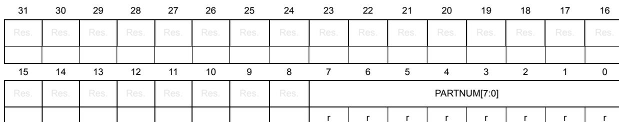
| 31 | 30 | 29 | 28 | 27 | 26 | 25 | 24 | 23 | 22 | 21 | 20 | 19 | 18 | 17 | 16 |
| Res. | Res. | Res. | Res. | Res. | Res. | Res. | Res. | Res. | Res. | Res. | Res. | Res. | Res. | Res. | Res. |
| 15 | 14 | 13 | 12 | 11 | 10 | 9 | 8 | 7 | 6 | 5 | 4 | 3 | 2 | 1 | 0 |
| Res. | Res. | Res. | Res. | Res. | Res. | Res. | Res. | PARTNUM[7:0] | |||||||
| r | r | r | r | r | r | r | r | ||||||||
Bits 31:8 Reserved, must be kept at reset value.
Bits 7:0 PARTNUM[7:0] : Part number field, bits [7:0]
0x12: TPIU part number
TPIU CoreSight peripheral identity register 1 (TPIU_PIDR1)
Address offset: 0xFE4
Reset value: 0x0000 00B9
| 31 | 30 | 29 | 28 | 27 | 26 | 25 | 24 | 23 | 22 | 21 | 20 | 19 | 18 | 17 | 16 |
|---|---|---|---|---|---|---|---|---|---|---|---|---|---|---|---|
| Res. | Res. | Res. | Res. | Res. | Res. | Res. | Res. | Res. | Res. | Res. | Res. | Res. | Res. | Res. | Res. |
| 15 | 14 | 13 | 12 | 11 | 10 | 9 | 8 | 7 | 6 | 5 | 4 | 3 | 2 | 1 | 0 |
| Res. | Res. | Res. | Res. | Res. | Res. | Res. | Res. | JEP106ID[3:0] | PARTNUM[11:8] | ||||||
| r | r | r | r | r | r | r | r | ||||||||
Bits 31:8 Reserved, must be kept at reset value.
Bits 7:4 JEP106ID[3:0] : JEP106 identity code field, bits [3:0]
0xB: Arm ® JEDEC code
Bits 3:0 PARTNUM[11:8] : Part number field, bits [11:8]
0x9: TPIU part number
TPIU CoreSight peripheral identity register 2 (TPIU_PIDR2)
Address offset: 0xFE8
Reset value: 0x0000 005B
| 31 | 30 | 29 | 28 | 27 | 26 | 25 | 24 | 23 | 22 | 21 | 20 | 19 | 18 | 17 | 16 |
|---|---|---|---|---|---|---|---|---|---|---|---|---|---|---|---|
| Res. | Res. | Res. | Res. | Res. | Res. | Res. | Res. | Res. | Res. | Res. | Res. | Res. | Res. | Res. | Res. |
| 15 | 14 | 13 | 12 | 11 | 10 | 9 | 8 | 7 | 6 | 5 | 4 | 3 | 2 | 1 | 0 |
| Res. | Res. | Res. | Res. | Res. | Res. | Res. | Res. | REVISION[3:0] | JEDEC | JEP106ID[6:4] | |||||
| r | r | r | r | r | r | r | r | ||||||||
Bits 31:8 Reserved, must be kept at reset value.
Bits 7:4 REVISION[3:0] : Component revision number
0x5: r1p0
Bit 3 JEDEC : JEDEC assigned value
1: Designer ID specified by JEDEC
Bits 2:0 JEP106ID[6:4] : JEP106 identity code field, bits [6:4]
0x3: Arm ® JEDEC code
TPIU CoreSight peripheral identity register 3 (TPIU_PIDR3)
Address offset: 0xFEC
Reset value: 0x0000 0000
| 31 | 30 | 29 | 28 | 27 | 26 | 25 | 24 | 23 | 22 | 21 | 20 | 19 | 18 | 17 | 16 |
|---|---|---|---|---|---|---|---|---|---|---|---|---|---|---|---|
| Res. | Res. | Res. | Res. | Res. | Res. | Res. | Res. | Res. | Res. | Res. | Res. | Res. | Res. | Res. | Res. |
| 15 | 14 | 13 | 12 | 11 | 10 | 9 | 8 | 7 | 6 | 5 | 4 | 3 | 2 | 1 | 0 |
| Res. | Res. | Res. | Res. | Res. | Res. | Res. | Res. | REVAND[3:0] | CMOD[3:0] | ||||||
| r | r | r | r | r | r | r | r | ||||||||
Bits 31:8 Reserved, must be kept at reset value.
Bits 7:4 REVAND[3:0] : Metal fix version
0x0: No metal fix
Bits 3:0 CMOD[3:0] : Customer modified
0x0: No customer modifications
TPIU CoreSight component identity register 0 (TPIU_CIDR0)
Address offset: 0xFF0
Reset value: 0x0000 000D
| 31 | 30 | 29 | 28 | 27 | 26 | 25 | 24 | 23 | 22 | 21 | 20 | 19 | 18 | 17 | 16 |
|---|---|---|---|---|---|---|---|---|---|---|---|---|---|---|---|
| Res. | Res. | Res. | Res. | Res. | Res. | Res. | Res. | Res. | Res. | Res. | Res. | Res. | Res. | Res. | Res. |
| 15 | 14 | 13 | 12 | 11 | 10 | 9 | 8 | 7 | 6 | 5 | 4 | 3 | 2 | 1 | 0 |
| Res. | Res. | Res. | Res. | Res. | Res. | Res. | Res. | PREAMBLE[7:0] | |||||||
| r | r | r | r | r | r | r | r | ||||||||
Bits 31:8 Reserved, must be kept at reset value.
Bits 7:0 PREAMBLE[7:0] : Component ID field, bits [7:0]
0x0D: Common ID value
TPIU CoreSight component identity register 1 (TPIU_CIDR1)
Address offset: 0xFF4
Reset value: 0x0000 0090
| 31 | 30 | 29 | 28 | 27 | 26 | 25 | 24 | 23 | 22 | 21 | 20 | 19 | 18 | 17 | 16 |
|---|---|---|---|---|---|---|---|---|---|---|---|---|---|---|---|
| Res. | Res. | Res. | Res. | Res. | Res. | Res. | Res. | Res. | Res. | Res. | Res. | Res. | Res. | Res. | Res. |
| 15 | 14 | 13 | 12 | 11 | 10 | 9 | 8 | 7 | 6 | 5 | 4 | 3 | 2 | 1 | 0 |
| Res. | Res. | Res. | Res. | Res. | Res. | Res. | Res. | ||||||||
| CLASS[3:0] | PREAMBLE[11:8] | ||||||||||||||
| r | r | r | r | r | r | r | r | ||||||||
Bits 31:8 Reserved, must be kept at reset value.
Bits 7:4
CLASS[3:0]
: Component ID field, bits [15:12] - component class
0x9: CoreSight component
Bits 3:0
PREAMBLE[11:8]
: Component ID field, bits [11:8]
0x0: Common ID value
TPIU CoreSight component identity register 2 (TPIU_CIDR2)
Address offset: 0xFF8
Reset value: 0x0000 0005
| 31 | 30 | 29 | 28 | 27 | 26 | 25 | 24 | 23 | 22 | 21 | 20 | 19 | 18 | 17 | 16 |
|---|---|---|---|---|---|---|---|---|---|---|---|---|---|---|---|
| Res. | Res. | Res. | Res. | Res. | Res. | Res. | Res. | Res. | Res. | Res. | Res. | Res. | Res. | Res. | Res. |
| 15 | 14 | 13 | 12 | 11 | 10 | 9 | 8 | 7 | 6 | 5 | 4 | 3 | 2 | 1 | 0 |
| Res. | Res. | Res. | Res. | Res. | Res. | Res. | Res. | ||||||||
| PREAMBLE[19:12] | |||||||||||||||
| r | r | r | r | r | r | r | r | ||||||||
Bits 31:8 Reserved, must be kept at reset value.
Bits 7:0
PREAMBLE[19:12]
: Component ID field, bits [23:16]
0x05: Common ID value
TPIU CoreSight component identity register 3 (TPIU_CIDR3)
Address offset: 0xFFC
Reset value: 0x0000 00B1
| 31 | 30 | 29 | 28 | 27 | 26 | 25 | 24 | 23 | 22 | 21 | 20 | 19 | 18 | 17 | 16 |
| Res. | Res. | Res. | Res. | Res. | Res. | Res. | Res. | Res. | Res. | Res. | Res. | Res. | Res. | Res. | Res. |
| 15 | 14 | 13 | 12 | 11 | 10 | 9 | 8 | 7 | 6 | 5 | 4 | 3 | 2 | 1 | 0 |
| Res. | Res. | Res. | Res. | Res. | Res. | Res. | Res. | PREAMBLE[27:20] | |||||||
| r | r | r | r | r | r | r | r | ||||||||
Bits 31:8 Reserved, must be kept at reset value.
Bits 7:0
PREAMBLE[27:20]
: Component ID field, bits [31:24]
0xB1: Common ID value
TPIU register map and reset values
Table 639. TPIU register map and reset values
| Offset | Register name | 31 | 30 | 29 | 28 | 27 | 26 | 25 | 24 | 23 | 22 | 21 | 20 | 19 | 18 | 17 | 16 | 15 | 14 | 13 | 12 | 11 | 10 | 9 | 8 | 7 | 6 | 5 | 4 | 3 | 2 | 1 | 0 | |
|---|---|---|---|---|---|---|---|---|---|---|---|---|---|---|---|---|---|---|---|---|---|---|---|---|---|---|---|---|---|---|---|---|---|---|
| 0x000 | TPIU_SUPPSIZE | PORTSIZE[31:0] | ||||||||||||||||||||||||||||||||
| Reset value | 0 | 0 | 0 | 0 | 0 | 0 | 0 | 0 | 0 | 0 | 0 | 0 | 0 | 0 | 0 | 0 | 0 | 0 | 0 | 0 | 0 | 0 | 0 | 0 | 1 | 1 | 1 | 1 | 1 | 1 | 1 | 1 | ||
| 0x004 | TPIU_CURPSIZE | PORTSIZE[31:0] | ||||||||||||||||||||||||||||||||
| Reset value | 0 | 0 | 0 | 0 | 0 | 0 | 0 | 0 | 0 | 0 | 0 | 0 | 0 | 0 | 0 | 0 | 0 | 0 | 0 | 0 | 0 | 0 | 0 | 0 | 0 | 0 | 0 | 0 | 0 | 0 | 0 | 1 | ||
| 0x008 to 0x0FC | Reserved | Reserved | ||||||||||||||||||||||||||||||||
| 0x100 | TPIU_SUPTRGM | Res. | Res. | Res. | Res. | Res. | Res. | Res. | Res. | Res. | Res. | Res. | Res. | Res. | Res. | TRGRUN | TRIGD | Res. | Res. | Res. | Res. | Res. | Res. | Res. | TCOUNT8 | Res. | Res. | Res. | MULT64K | MULT256 | MULT16 | MULT4 | MULT2 | |
| Reset value | 0 | 0 | 1 | 1 | 1 | 1 | 1 | 1 | ||||||||||||||||||||||||||
| 0x104 | TPIU_TRGCNT | Res. | Res. | Res. | Res. | Res. | Res. | Res. | Res. | Res. | Res. | Res. | Res. | Res. | Res. | Res. | Res. | Res. | Res. | Res. | Res. | Res. | Res. | Res. | Res. | TRIGCOUNT[7:0] | ||||||||
| Reset value | 0 | 0 | 0 | 0 | 0 | 0 | 0 | 0 | ||||||||||||||||||||||||||
| 0x108 | TPIU_TRGMULT | Res. | Res. | Res. | Res. | Res. | Res. | Res. | Res. | Res. | Res. | Res. | Res. | Res. | Res. | Res. | Res. | Res. | Res. | Res. | Res. | Res. | Res. | Res. | Res. | Res. | Res. | Res. | MULT64K | MULT256 | MULT16 | MULT4 | MULT2 | |
| Reset value | 0 | 0 | 0 | 0 | 0 | |||||||||||||||||||||||||||||
| 0x10C to 0x1FC | Reserved | Reserved | ||||||||||||||||||||||||||||||||
| 0x200 | TPIU_SUPTPM | Res. | Res. | Res. | Res. | Res. | Res. | Res. | Res. | Res. | Res. | Res. | Res. | Res. | Res. | PCONTEN | PTMEEN | Res. | Res. | Res. | Res. | Res. | Res. | Res. | Res. | Res. | Res. | Res. | Res. | Res. | PATF0 | PATA5 | PATW0 | PATW1 |
| Reset value | 1 | 1 | 1 | 1 | 1 | 1 | ||||||||||||||||||||||||||||
| 0x204 | TPIU_CURTPM | Res. | Res. | Res. | Res. | Res. | Res. | Res. | Res. | Res. | Res. | Res. | Res. | Res. | Res. | PCONTEN | PTMEEN | Res. | Res. | Res. | Res. | Res. | Res. | Res. | Res. | Res. | Res. | Res. | Res. | Res. | PATF0 | PATA5 | PATW0 | PATW1 |
| Reset value | 0 | 0 | 0 | 0 | 0 | 0 | ||||||||||||||||||||||||||||
Table 639. TPIU register map and reset values (continued)
| Offset | Register name | 31 | 30 | 29 | 28 | 27 | 26 | 25 | 24 | 23 | 22 | 21 | 20 | 19 | 18 | 17 | 16 | 15 | 14 | 13 | 12 | 11 | 10 | 9 | 8 | 7 | 6 | 5 | 4 | 3 | 2 | 1 | 0 | |||
|---|---|---|---|---|---|---|---|---|---|---|---|---|---|---|---|---|---|---|---|---|---|---|---|---|---|---|---|---|---|---|---|---|---|---|---|---|
| 0x208 | TPIU_TPRCR | Res. | Res. | Res. | Res. | Res. | Res. | Res. | Res. | Res. | Res. | Res. | Res. | Res. | Res. | Res. | Res. | Res. | Res. | Res. | Res. | Res. | Res. | Res. | Res. | PATTCOUNT[7:0] | ||||||||||
| Reset value | 0 | 0 | 0 | 0 | 0 | 0 | 0 | 0 | ||||||||||||||||||||||||||||
| 0x20C to 0x2FC | Reserved | Reserved | ||||||||||||||||||||||||||||||||||
| 0x300 | TPIU_FFSR | Res. | Res. | Res. | Res. | Res. | Res. | Res. | Res. | Res. | Res. | Res. | Res. | Res. | Res. | Res. | Res. | Res. | Res. | Res. | Res. | Res. | Res. | Res. | Res. | Res. | Res. | Res. | Res. | Res. | TCPRESENT | FTSTOPPED | FLINPROG | |||
| Reset value | 0 | 1 | 0 | |||||||||||||||||||||||||||||||||
| 0x304 | TPIU_FFCR | Res. | Res. | Res. | Res. | Res. | Res. | Res. | Res. | Res. | Res. | Res. | Res. | Res. | Res. | Res. | Res. | Res. | Res. | STOPTRIG | STOPFL | Res. | Res. | TRIGFL | TRIGEVt | TRIGIN | Res. | FONMAN | FONTRIG | FONFLIN | Res. | Res. | ENFCONT | ENFTC | ||
| Reset value | 0 | 0 | 0 | 0 | 0 | 0 | 0 | 0 | 0 | 0 | ||||||||||||||||||||||||||
| 0x308 | TPIU_FSCR | Res. | Res. | Res. | Res. | Res. | Res. | Res. | Res. | Res. | Res. | Res. | Res. | Res. | Res. | Res. | Res. | Res. | Res. | Res. | Res. | CYCCOUNT[11:0] | ||||||||||||||
| Reset value | 0 | 0 | 0 | 0 | 0 | 1 | 0 | 0 | 0 | 0 | 0 | 0 | ||||||||||||||||||||||||
| 0x30C to 0xF9C | Reserved | Reserved | ||||||||||||||||||||||||||||||||||
| 0xFA0 | TPIU_CLAIMSET | Res. | Res. | Res. | Res. | Res. | Res. | Res. | Res. | Res. | Res. | Res. | Res. | Res. | Res. | Res. | Res. | Res. | Res. | Res. | Res. | Res. | Res. | Res. | Res. | Res. | Res. | Res. | Res. | CLAIMSET[3:0] | ||||||
| Reset value | 1 | 1 | 1 | 1 | ||||||||||||||||||||||||||||||||
| 0xFA4 | TPIU_CLAIMCLR | Res. | Res. | Res. | Res. | Res. | Res. | Res. | Res. | Res. | Res. | Res. | Res. | Res. | Res. | Res. | Res. | Res. | Res. | Res. | Res. | Res. | Res. | Res. | Res. | Res. | Res. | Res. | Res. | CLAIMCLR[3:0] | ||||||
| Reset value | 0 | 0 | 0 | 0 | ||||||||||||||||||||||||||||||||
| 0xFB0 | TPIU_LAR | ACCESS_W[31:0] | ||||||||||||||||||||||||||||||||||
| Reset value | - | - | - | - | - | - | - | - | - | - | - | - | - | - | - | - | - | - | - | - | - | - | - | - | - | - | - | - | - | - | - | - | ||||
| 0xFB4 | TPIU_LSR | Res. | Res. | Res. | Res. | Res. | Res. | Res. | Res. | Res. | Res. | Res. | Res. | Res. | Res. | Res. | Res. | Res. | Res. | Res. | Res. | Res. | Res. | Res. | Res. | Res. | Res. | Res. | Res. | Res. | LOCKTYPE | LOCKGRANT | LOCKEXIST | |||
| Reset value | 0 | 1 | 1 | |||||||||||||||||||||||||||||||||
| 0xFB8 | TPIU_AUTHSTAT | Res. | Res. | Res. | Res. | Res. | Res. | Res. | Res. | Res. | Res. | Res. | Res. | Res. | Res. | Res. | Res. | Res. | Res. | Res. | Res. | Res. | Res. | Res. | Res. | SNID[1:0] | Res. | SID[1:0] | Res. | NSNID[1:0] | Res. | NSID[1:0] | ||||
| Reset value | 0 | 0 | 0 | 0 | 0 | 0 | 0 | 0 | ||||||||||||||||||||||||||||
| 0xFBC to 0xFC4 | Reserved | Reserved | ||||||||||||||||||||||||||||||||||
| 0xFC8 | TPIU_DEVID | Res. | Res. | Res. | Res. | Res. | Res. | Res. | Res. | Res. | Res. | Res. | Res. | Res. | Res. | Res. | Res. | Res. | Res. | Res. | Res. | SWOUARTNRZ | SWOMAN | TCLKDATA | Res. | FIFOSIZE[2:0] | Res. | CLKRELAT | MUXNUM[4:0] | |||||||
| Reset value | 0 | 0 | 0 | 0 | 1 | 0 | 1 | 0 | 0 | 0 | 0 | 0 | ||||||||||||||||||||||||
Table 639. TPIU register map and reset values (continued)
| Offset | Register name | 31 | 30 | 29 | 28 | 27 | 26 | 25 | 24 | 23 | 22 | 21 | 20 | 19 | 18 | 17 | 16 | 15 | 14 | 13 | 12 | 11 | 10 | 9 | 8 | 7 | 6 | 5 | 4 | 3 | 2 | 1 | 0 | |||||
|---|---|---|---|---|---|---|---|---|---|---|---|---|---|---|---|---|---|---|---|---|---|---|---|---|---|---|---|---|---|---|---|---|---|---|---|---|---|---|
| 0xFCC | TPIU_DEVTYPE | Res. | Res. | Res. | Res. | Res. | Res. | Res. | Res. | Res. | Res. | Res. | Res. | Res. | Res. | Res. | Res. | Res. | Res. | Res. | Res. | Res. | Res. | Res. | Res. | Res. | SUBTYPE[3:0] | MAJORTYP[3:0] | ||||||||||
| Reset value | 0 | 0 | 0 | 1 | 0 | 0 | 0 | 1 | ||||||||||||||||||||||||||||||
| 0xFD0 | TPIU_PIDR4 | Res. | Res. | Res. | Res. | Res. | Res. | Res. | Res. | Res. | Res. | Res. | Res. | Res. | Res. | Res. | Res. | Res. | Res. | Res. | Res. | Res. | Res. | Res. | Res. | Res. | 4KCOUNT[3:0] | JEP106CON[3:0] | ||||||||||
| Reset value | 0 | 0 | 0 | 0 | 0 | 1 | 0 | 0 | ||||||||||||||||||||||||||||||
| 0xFD4 to 0xFDC | Reserved | Reserved | ||||||||||||||||||||||||||||||||||||
| 0xFE0 | TPIU_PIDR0 | Res. | Res. | Res. | Res. | Res. | Res. | Res. | Res. | Res. | Res. | Res. | Res. | Res. | Res. | Res. | Res. | Res. | Res. | Res. | Res. | Res. | Res. | Res. | Res. | Res. | Res. | Res. | Res. | Res. | Res. | Res. | PARTNUM[7:0] | |||||
| Reset value | 0 | 0 | 0 | 1 | 0 | 0 | 1 | 0 | ||||||||||||||||||||||||||||||
| 0xFE4 | TPIU_PIDR1 | Res. | Res. | Res. | Res. | Res. | Res. | Res. | Res. | Res. | Res. | Res. | Res. | Res. | Res. | Res. | Res. | Res. | Res. | Res. | Res. | Res. | Res. | Res. | Res. | Res. | Res. | JEP106ID[3:0] | PARTNUM[11:8] | |||||||||
| Reset value | 1 | 0 | 1 | 1 | 1 | 0 | 0 | 1 | ||||||||||||||||||||||||||||||
| 0xFE8 | TPIU_PIDR2 | Res. | Res. | Res. | Res. | Res. | Res. | Res. | Res. | Res. | Res. | Res. | Res. | Res. | Res. | Res. | Res. | Res. | Res. | Res. | Res. | Res. | Res. | Res. | Res. | Res. | Res. | REVISION[3:0] | JEDEC | JEP106ID[6:4] | ||||||||
| Reset value | 0 | 1 | 0 | 1 | 1 | 0 | 1 | 1 | ||||||||||||||||||||||||||||||
| 0xFEC | TPIU_PIDR3 | Res. | Res. | Res. | Res. | Res. | Res. | Res. | Res. | Res. | Res. | Res. | Res. | Res. | Res. | Res. | Res. | Res. | Res. | Res. | Res. | Res. | Res. | Res. | Res. | Res. | Res. | REVAND[3:0] | CMOD[3:0] | |||||||||
| Reset value | 0 | 0 | 0 | 0 | 0 | 0 | 0 | 0 | ||||||||||||||||||||||||||||||
| 0xFF0 | TPIU_CIDR0 | Res. | Res. | Res. | Res. | Res. | Res. | Res. | Res. | Res. | Res. | Res. | Res. | Res. | Res. | Res. | Res. | Res. | Res. | Res. | Res. | Res. | Res. | Res. | Res. | Res. | Res. | Res. | Res. | Res. | Res. | Res. | PREAMBLE[7:0] | |||||
| Reset value | 0 | 0 | 0 | 0 | 1 | 1 | 0 | 1 | ||||||||||||||||||||||||||||||
| 0xFF4 | TPIU_CIDR1 | Res. | Res. | Res. | Res. | Res. | Res. | Res. | Res. | Res. | Res. | Res. | Res. | Res. | Res. | Res. | Res. | Res. | Res. | Res. | Res. | Res. | Res. | Res. | Res. | Res. | Res. | Res. | CLASS[3:0] | PREAMBLE[11:8] | ||||||||
| Reset value | 1 | 0 | 0 | 1 | 0 | 0 | 0 | 0 | ||||||||||||||||||||||||||||||
| 0xFF8 | TPIU_CIDR2 | Res. | Res. | Res. | Res. | Res. | Res. | Res. | Res. | Res. | Res. | Res. | Res. | Res. | Res. | Res. | Res. | Res. | Res. | Res. | Res. | Res. | Res. | Res. | Res. | Res. | Res. | Res. | Res. | Res. | Res. | Res. | PREAMBLE[19:12] | |||||
| Reset value | 0 | 0 | 0 | 0 | 0 | 1 | 0 | 1 | ||||||||||||||||||||||||||||||
| 0xFFC | TPIU_CIDR3 | Res. | Res. | Res. | Res. | Res. | Res. | Res. | Res. | Res. | Res. | Res. | Res. | Res. | Res. | Res. | Res. | Res. | Res. | Res. | Res. | Res. | Res. | Res. | Res. | Res. | Res. | Res. | Res. | Res. | Res. | Res. | PREAMBLE[27:20] | |||||
| Reset value | 1 | 0 | 1 | 1 | 0 | 0 | 0 | 1 | ||||||||||||||||||||||||||||||
63.5.7 Serial wire output (SWO) and SWO trace funnel (SWTF)
The SWO is a CoreSight component that formats the trace stream from the processor ITM and outputs it on the single wire TRACESWO output. The trace source identity is not handled by the SWO, so only one processor can use the SWO at a time. The SWO trace funnel (SWTF) must be programmed to select which processor ITM will use it before trace is enabled. Port 0 is connected to the Cortex-M7 and Port 1 to the Cortex-M4. The SWTF registers are listed in Table 641 .
Compared to the TPIU, the SWO contains:
- • no formatter
- • no pattern generator
- • an 8-bit ATB input
- • no synchronous trace output, that is, no TRACEDATA or TRACECLK pins
- • no support for flush, because this is not required
- • no support for triggering
The SWO output supports Manchester encoded and UART NRZ formats.
For more information about the serial wire output CoreSight™ component, refer to the Arm® CoreSight™ Components Technical Reference Manual [4].
SWO registers
SWO current output divisor register (SWO_CODR)
Address offset: 0x010
Reset value: 0x0000 0000
| 31 | 30 | 29 | 28 | 27 | 26 | 25 | 24 | 23 | 22 | 21 | 20 | 19 | 18 | 17 | 16 |
|---|---|---|---|---|---|---|---|---|---|---|---|---|---|---|---|
| Res. | Res. | Res. | Res. | Res. | Res. | Res. | Res. | Res. | Res. | Res. | Res. | Res. | Res. | Res. | Res. |
| 15 | 14 | 13 | 12 | 11 | 10 | 9 | 8 | 7 | 6 | 5 | 4 | 3 | 2 | 1 | 0 |
| Res. | Res. | Res. | PRESCALER[12:0] | ||||||||||||
| rw | rw | rw | rw | rw | rw | rw | rw | rw | rw | rw | rw | rw | |||
Bits 31:13 Reserved, must be kept at reset value.
Bits 12:0 PRESCALER[12:0] : SWO baud rate scaling
The baud rate is the trace clock frequency divided by (PRESCALER + 1). The baud rate changes instantly, so it is recommended to stop the trace source and wait until the port is idle before writing to this register.
SWO selected pin protocol register (SWO_SPPR)
Address offset: 0x0F0
Reset value: 0x0000 0001
| 31 | 30 | 29 | 28 | 27 | 26 | 25 | 24 | 23 | 22 | 21 | 20 | 19 | 18 | 17 | 16 |
|---|---|---|---|---|---|---|---|---|---|---|---|---|---|---|---|
| Res. | Res. | Res. | Res. | Res. | Res. | Res. | Res. | Res. | Res. | Res. | Res. | Res. | Res. | Res. | Res. |
| 15 | 14 | 13 | 12 | 11 | 10 | 9 | 8 | 7 | 6 | 5 | 4 | 3 | 2 | 1 | 0 |
| Res. | Res. | Res. | Res. | Res. | Res. | Res. | Res. | PPROT[1:0] | |||||||
| rw | rw | ||||||||||||||
Bits 31:2 Reserved, must be kept at reset value.
Bits 1:0 PPROT[1:0] : Pin protocol
- 0x0: Reserved
- 0x1: Manchester
- 0x2: NRZ
- 0x3: Reserved
SWO formatter and flush status register (SWO_FFSR)
Address offset: 0x300
Reset value: 0x0000 0008
| 31 | 30 | 29 | 28 | 27 | 26 | 25 | 24 | 23 | 22 | 21 | 20 | 19 | 18 | 17 | 16 |
|---|---|---|---|---|---|---|---|---|---|---|---|---|---|---|---|
| Res. | Res. | Res. | Res. | Res. | Res. | Res. | Res. | Res. | Res. | Res. | Res. | Res. | Res. | Res. | Res. |
| 15 | 14 | 13 | 12 | 11 | 10 | 9 | 8 | 7 | 6 | 5 | 4 | 3 | 2 | 1 | 0 |
| Res. | Res. | Res. | Res. | Res. | Res. | Res. | Res. | Res. | Res. | Res. | Res. | FTNON STOP | TCPRE SENT | FTSTO PPED | FLINPR OG |
| r | r | r | r | ||||||||||||
Bits 31:4 Reserved, must be kept at reset value.
Bit 3 FTNONSTOP : Change of settings without stopping formatter
1: Change of settings is allowed with formatter running
Bit 2 TCPPRESENT : TRACECTL pin present on SWO
0: TRACECTL pin not present
Bit 1 FTSTOPPED : Formatter stopped
0: Formatter running
The bit always returns 0 as the SWO formatter cannot be stopped in this device.
Bit 0 FLINPROG : Flush in progress
0: Flush is not in progress
The bit always returns 0 as SWO flushing is not supported in this device.
SWO claim tag set register (SWO_CLAIMSET)
Address offset: 0xFA0
Reset value: 0x0000 000F
| 31 | 30 | 29 | 28 | 27 | 26 | 25 | 24 | 23 | 22 | 21 | 20 | 19 | 18 | 17 | 16 |
|---|---|---|---|---|---|---|---|---|---|---|---|---|---|---|---|
| Res. | Res. | Res. | Res. | Res. | Res. | Res. | Res. | Res. | Res. | Res. | Res. | Res. | Res. | Res. | Res. |
| 15 | 14 | 13 | 12 | 11 | 10 | 9 | 8 | 7 | 6 | 5 | 4 | 3 | 2 | 1 | 0 |
| Res. | Res. | Res. | Res. | Res. | Res. | Res. | Res. | Res. | Res. | Res. | Res. | CLAIMSET[3:0] | |||
| rw | rw | rw | rw | ||||||||||||
Bits 31:4 Reserved, must be kept at reset value.
Bits 3:0 CLAIMSET[3:0] : Set claim tag bits
Write:
0000: No effect
xxx1: Set bit 0
xx1x: Set bit 1
x1xx: Set bit 2
1xxx: Set bit 3
Read:
0xF: Indicates there are four bits in claim tag
SWO claim tag clear register (SWO_CLAIMCLR)
Address offset: 0xFA4
Reset value: 0x0000 0000
| 31 | 30 | 29 | 28 | 27 | 26 | 25 | 24 | 23 | 22 | 21 | 20 | 19 | 18 | 17 | 16 |
|---|---|---|---|---|---|---|---|---|---|---|---|---|---|---|---|
| Res. | Res. | Res. | Res. | Res. | Res. | Res. | Res. | Res. | Res. | Res. | Res. | Res. | Res. | Res. | Res. |
| 15 | 14 | 13 | 12 | 11 | 10 | 9 | 8 | 7 | 6 | 5 | 4 | 3 | 2 | 1 | 0 |
| Res. | Res. | Res. | Res. | Res. | Res. | Res. | Res. | Res. | Res. | Res. | Res. | CLAIMCLR[3:0] | |||
| rw | rw | rw | rw | ||||||||||||
Bits 31:4 Reserved, must be kept at reset value.
Bits 3:0 CLAIMCLR[3:0] : Reset claim tag bits
Write:
0000: No effect
xxx1: Clear bit 0
xx1x: Clear bit 1
x1xx: Clear bit 2
1xxx: Clear bit 3
Read: Returns current value of claim tag
SWO lock access register (SWO_LAR)
Address offset: 0xFB0
Reset value: N/A
| 31 | 30 | 29 | 28 | 27 | 26 | 25 | 24 | 23 | 22 | 21 | 20 | 19 | 18 | 17 | 16 |
|---|---|---|---|---|---|---|---|---|---|---|---|---|---|---|---|
| ACCESS_W[31:16] | |||||||||||||||
| w | w | w | w | w | w | w | w | w | w | w | w | w | w | w | w |
| 15 | 14 | 13 | 12 | 11 | 10 | 9 | 8 | 7 | 6 | 5 | 4 | 3 | 2 | 1 | 0 |
| ACCESS_W[15:0] | |||||||||||||||
| w | w | w | w | w | w | w | w | w | w | w | w | w | w | w | w |
Bits 31:0 ACCESS_W[31:0] : SWO register write access enable
Enables write access to some SWO registers by processor cores (debuggers do not need to unlock the component)
0xC5ACCE55: Enable write access
Other values: Disable write access
SWO lock status register (SWO_LSR)
Address offset: 0xFB4
Reset value: 0x0000 0003
| 31 | 30 | 29 | 28 | 27 | 26 | 25 | 24 | 23 | 22 | 21 | 20 | 19 | 18 | 17 | 16 |
|---|---|---|---|---|---|---|---|---|---|---|---|---|---|---|---|
| Res. | Res. | Res. | Res. | Res. | Res. | Res. | Res. | Res. | Res. | Res. | Res. | Res. | Res. | Res. | Res. |
| 15 | 14 | 13 | 12 | 11 | 10 | 9 | 8 | 7 | 6 | 5 | 4 | 3 | 2 | 1 | 0 |
| Res. | Res. | Res. | Res. | Res. | Res. | Res. | Res. | Res. | Res. | Res. | Res. | Res. | LOCKTYPE | LOCKGRANT | LOCKEXIST |
| r | r | r |
Bits 31:3 Reserved, must be kept at reset value.
Bit 2 LOCKTYPE : Size of the SWO_LAR register
0: 32-bit
Bit 1 LOCKGRANT : Current status of lock
This bit always returns zero when read by an external debugger.
0: Write access is permitted
1: Write access is blocked - only read access is permitted
Bit 0 LOCKEXIST : Implementation of a lock control mechanism
The bit indicates whether a lock control mechanism is implemented. It always returns zero when read by an external debugger.
0: No lock control mechanism is available
1: Lock control mechanism is implemented
SWO authentication status register (SWO_AUTHSTAT)
Address offset: 0xFB8
Reset value: 0x0000 0000
| 31 | 30 | 29 | 28 | 27 | 26 | 25 | 24 | 23 | 22 | 21 | 20 | 19 | 18 | 17 | 16 |
|---|---|---|---|---|---|---|---|---|---|---|---|---|---|---|---|
| Res. | Res. | Res. | Res. | Res. | Res. | Res. | Res. | Res. | Res. | Res. | Res. | Res. | Res. | Res. | Res. |
| 15 | 14 | 13 | 12 | 11 | 10 | 9 | 8 | 7 | 6 | 5 | 4 | 3 | 2 | 1 | 0 |
| Res. | Res. | Res. | Res. | Res. | Res. | Res. | Res. | SNID[1:0] | SID[1:0] | NSNID[1:0] | NSID[1:0] | ||||
| r | r | r | r | r | r | r | r |
- Bits 31:8 Reserved, must be kept at reset value.
- Bits 7:6
SNID[1:0]
: Security level for secure non-invasive debug
0x0: Not implemented - Bits 5:4
SID[1:0]
: Security level for secure invasive debug
0x0: Not implemented - Bits 3:2
NSNID[1:0]
: Security level for non-secure non-invasive debug
0x0: Not implemented - Bits 1:0
NSID[1:0]
: Security level for non-secure invasive debug
0x0: Not implemented
SWO device configuration register (SWO_DEVID)
Address offset: 0xFC8
Reset value: 0x0000 0EA0
| 31 | 30 | 29 | 28 | 27 | 26 | 25 | 24 | 23 | 22 | 21 | 20 | 19 | 18 | 17 | 16 |
|---|---|---|---|---|---|---|---|---|---|---|---|---|---|---|---|
| Res. | Res. | Res. | Res. | Res. | Res. | Res. | Res. | Res. | Res. | Res. | Res. | Res. | Res. | Res. | Res. |
| 15 | 14 | 13 | 12 | 11 | 10 | 9 | 8 | 7 | 6 | 5 | 4 | 3 | 2 | 1 | 0 |
| Res. | Res. | Res. | Res. | SWO UART NRZ | SWO MAN | TCLK DATA | FIFO SIZE[2:0] | CLK RELAT | MUXNUM[4:0] | ||||||
| r | r | r | r | r | r | r | r | r | r | r | r | ||||
- Bits 31:11 Reserved, must be kept at reset value.
- Bit 11
SWOUARTNRZ
: SWO UART or NRZ support
Indicates whether serial wire output, UART or NRZ, is supported.
1: Supported - Bit 10
SWOMAN
: SWO Manchester format support
Indicates whether serial wire output, Manchester encoded format, is supported.
1: Supported - Bit 9
TCLKDATA
: Trace clock plus data support
Indicates whether trace clock plus data is supported
1: Supported - Bits 8:6
FIFOSIZE[2:0]
: FIFO size in powers of 2
0x2: FIFO size = 4 (16 bytes) - Bit 5
CLKRELAT
: ATB clock to TRACECLKIN relation
Indicates the relationship between the ATB clock and TRACECLKIN (synchronous or asynchronous)
1: Asynchronous - Bits 4:0
MUXNUM[4:0]
: Number/type of ATB input port multiplexing
0x0: None
SWO device type identifier register (SWO_DEVTYPE)
Address offset: 0xFCC
Reset value: 0x0000 0011
| 31 | 30 | 29 | 28 | 27 | 26 | 25 | 24 | 23 | 22 | 21 | 20 | 19 | 18 | 17 | 16 |
|---|---|---|---|---|---|---|---|---|---|---|---|---|---|---|---|
| Res. | Res. | Res. | Res. | Res. | Res. | Res. | Res. | Res. | Res. | Res. | Res. | Res. | Res. | Res. | Res. |
| 15 | 14 | 13 | 12 | 11 | 10 | 9 | 8 | 7 | 6 | 5 | 4 | 3 | 2 | 1 | 0 |
| Res. | Res. | Res. | Res. | Res. | Res. | Res. | Res. | SUBTYPE[3:0] | MAJORTYPE[3:0] | ||||||
| r | r | r | r | r | r | r | r | ||||||||
Bits 31:8 Reserved, must be kept at reset value.
Bits 7:4 SUBTYPE[3:0] : Sub-classification
0x1: Trace port component
Bits 3:0 MAJORTYPE[3:0] : Major classification
0x1: Trace sink component
SWO CoreSight peripheral identity register 4 (SWO_PIDR4)
Address offset: 0xFD0
Reset value: 0x0000 0004
| 31 | 30 | 29 | 28 | 27 | 26 | 25 | 24 | 23 | 22 | 21 | 20 | 19 | 18 | 17 | 16 |
|---|---|---|---|---|---|---|---|---|---|---|---|---|---|---|---|
| Res. | Res. | Res. | Res. | Res. | Res. | Res. | Res. | Res. | Res. | Res. | Res. | Res. | Res. | Res. | Res. |
| 15 | 14 | 13 | 12 | 11 | 10 | 9 | 8 | 7 | 6 | 5 | 4 | 3 | 2 | 1 | 0 |
| Res. | Res. | Res. | Res. | Res. | Res. | Res. | Res. | 4KCOUNT[3:0] | JEP106CON[3:0] | ||||||
| r | r | r | r | r | r | r | r | ||||||||
Bits 31:8 Reserved, must be kept at reset value.
Bits 7:4 4KCOUNT[3:0] : Register file size
0x0: Register file occupies a single 4 Kbyte region
Bits 3:0 JEP106CON[3:0] : JEP106 continuation code
0x4: Arm ® JEDEC code
SWO CoreSight peripheral identity register 0 (SWO_PIDR0)Address offset: 0xFE0
Reset value: 0x0000 0014
| 31 | 30 | 29 | 28 | 27 | 26 | 25 | 24 | 23 | 22 | 21 | 20 | 19 | 18 | 17 | 16 |
|---|---|---|---|---|---|---|---|---|---|---|---|---|---|---|---|
| Res. | Res. | Res. | Res. | Res. | Res. | Res. | Res. | Res. | Res. | Res. | Res. | Res. | Res. | Res. | Res. |
| 15 | 14 | 13 | 12 | 11 | 10 | 9 | 8 | 7 | 6 | 5 | 4 | 3 | 2 | 1 | 0 |
| Res. | Res. | Res. | Res. | Res. | Res. | Res. | Res. | PARTNUM[7:0] | |||||||
| r | r | r | r | r | r | r | r | ||||||||
Bits 31:8 Reserved, must be kept at reset value.
Bits 7:0 PARTNUM[7:0] : Part number field, bits [7:0]0x14: SWO part number
SWO CoreSight peripheral identity register 1 (SWO_PIDR1)Address offset: 0xFE4
Reset value: 0x0000 00B9
| 31 | 30 | 29 | 28 | 27 | 26 | 25 | 24 | 23 | 22 | 21 | 20 | 19 | 18 | 17 | 16 |
|---|---|---|---|---|---|---|---|---|---|---|---|---|---|---|---|
| Res. | Res. | Res. | Res. | Res. | Res. | Res. | Res. | Res. | Res. | Res. | Res. | Res. | Res. | Res. | Res. |
| 15 | 14 | 13 | 12 | 11 | 10 | 9 | 8 | 7 | 6 | 5 | 4 | 3 | 2 | 1 | 0 |
| Res. | Res. | Res. | Res. | Res. | Res. | Res. | Res. | JEP106ID[3:0] | PARTNUM[11:8] | ||||||
| r | r | r | r | r | r | r | r | ||||||||
Bits 31:8 Reserved, must be kept at reset value.
Bits 7:4 JEP106ID[3:0] : JEP106 identity code field, bits [3:0]0xB: Arm® JEDEC code
Bits 3:0 PARTNUM[11:8] : Part number field, bits [11:8]0x9: SWO part number
SWO CoreSight peripheral identity register 2 (SWO_PIDR2)
Address offset: 0xFE8
Reset value: 0x0000 002B
| 31 | 30 | 29 | 28 | 27 | 26 | 25 | 24 | 23 | 22 | 21 | 20 | 19 | 18 | 17 | 16 |
|---|---|---|---|---|---|---|---|---|---|---|---|---|---|---|---|
| Res. | Res. | Res. | Res. | Res. | Res. | Res. | Res. | Res. | Res. | Res. | Res. | Res. | Res. | Res. | Res. |
| 15 | 14 | 13 | 12 | 11 | 10 | 9 | 8 | 7 | 6 | 5 | 4 | 3 | 2 | 1 | 0 |
| Res. | Res. | Res. | Res. | Res. | Res. | Res. | Res. | REVISION[3:0] | JEDEC | JEP106ID[6:4] | |||||
| r | r | r | r | r | r | r | r | ||||||||
Bits 31:8 Reserved, must be kept at reset value.
Bits 7:4 REVISION[3:0] : Component revision number
0x2: r0p2
Bit 3 JEDEC : JEDEC assigned value
1: Designer ID specified by JEDEC
Bits 2:0 JEP106ID[6:4] : JEP106 identity code field, bits [6:4]
0x3: Arm® JEDEC code
SWO CoreSight peripheral identity register 3 (SWO_PIDR3)
Address offset: 0xFEC
Reset value: 0x0000 0000
| 31 | 30 | 29 | 28 | 27 | 26 | 25 | 24 | 23 | 22 | 21 | 20 | 19 | 18 | 17 | 16 |
|---|---|---|---|---|---|---|---|---|---|---|---|---|---|---|---|
| Res. | Res. | Res. | Res. | Res. | Res. | Res. | Res. | Res. | Res. | Res. | Res. | Res. | Res. | Res. | Res. |
| 15 | 14 | 13 | 12 | 11 | 10 | 9 | 8 | 7 | 6 | 5 | 4 | 3 | 2 | 1 | 0 |
| Res. | Res. | Res. | Res. | Res. | Res. | Res. | Res. | REVAND[3:0] | CMOD[3:0] | ||||||
| r | r | r | r | r | r | r | r | ||||||||
Bits 31:8 Reserved, must be kept at reset value.
Bits 7:4 REVAND[3:0] : Metal fix version
0x0: No metal fix
Bits 3:0 CMOD[3:0] : Customer modified
0x0: No customer modifications
SWO CoreSight component identity register 0 (SWO_CIDR0)
Address offset: 0xFF0
Reset value: 0x0000 000D
| 31 | 30 | 29 | 28 | 27 | 26 | 25 | 24 | 23 | 22 | 21 | 20 | 19 | 18 | 17 | 16 |
|---|---|---|---|---|---|---|---|---|---|---|---|---|---|---|---|
| Res. | Res. | Res. | Res. | Res. | Res. | Res. | Res. | Res. | Res. | Res. | Res. | Res. | Res. | Res. | Res. |
| 15 | 14 | 13 | 12 | 11 | 10 | 9 | 8 | 7 | 6 | 5 | 4 | 3 | 2 | 1 | 0 |
| Res. | Res. | Res. | Res. | Res. | Res. | Res. | Res. | PREAMBLE[7:0] | |||||||
| r | r | r | r | r | r | r | r | ||||||||
Bits 31:8 Reserved, must be kept at reset value.
Bits 7:0 PREAMBLE[7:0] : Component ID field, bits [7:0]
0x0D: Common ID value
SWO CoreSight component identity register 1 (SWO_CIDR1)
Address offset: 0xFF4
Reset value: 0x0000 0090
| 31 | 30 | 29 | 28 | 27 | 26 | 25 | 24 | 23 | 22 | 21 | 20 | 19 | 18 | 17 | 16 |
|---|---|---|---|---|---|---|---|---|---|---|---|---|---|---|---|
| Res. | Res. | Res. | Res. | Res. | Res. | Res. | Res. | Res. | Res. | Res. | Res. | Res. | Res. | Res. | Res. |
| 15 | 14 | 13 | 12 | 11 | 10 | 9 | 8 | 7 | 6 | 5 | 4 | 3 | 2 | 1 | 0 |
| Res. | Res. | Res. | Res. | Res. | Res. | Res. | Res. | CLASS[3:0] | PREAMBLE[11:8] | ||||||
| r | r | r | r | r | r | r | r | ||||||||
Bits 31:8 Reserved, must be kept at reset value.
Bits 7:4 CLASS[3:0] : Component ID field, bits [15:12] - component class
0x9: CoreSight component
Bits 3:0 PREAMBLE[11:8] : Component ID field, bits [11:8]
0x0: Common ID value
SWO CoreSight component identity register 2 (SWO_CIDR2)
Address offset: 0xFF8
Reset value: 0x0000 0005
| 31 | 30 | 29 | 28 | 27 | 26 | 25 | 24 | 23 | 22 | 21 | 20 | 19 | 18 | 17 | 16 |
|---|---|---|---|---|---|---|---|---|---|---|---|---|---|---|---|
| Res. | Res. | Res. | Res. | Res. | Res. | Res. | Res. | Res. | Res. | Res. | Res. | Res. | Res. | Res. | Res. |
| 15 | 14 | 13 | 12 | 11 | 10 | 9 | 8 | 7 | 6 | 5 | 4 | 3 | 2 | 1 | 0 |
| Res. | Res. | Res. | Res. | Res. | Res. | Res. | Res. | PREAMBLE[19:12] | |||||||
| r | r | r | r | r | r | r | r | ||||||||
Bits 31:8 Reserved, must be kept at reset value.
Bits 7:0
PREAMBLE[19:12]
: Component ID field, bits [23:16]
0x05: Common ID value
SWO CoreSight component identity register 3 (SWO_CIDR3)
Address offset: 0xFFC
Reset value: 0x0000 00B1
| 31 | 30 | 29 | 28 | 27 | 26 | 25 | 24 | 23 | 22 | 21 | 20 | 19 | 18 | 17 | 16 |
|---|---|---|---|---|---|---|---|---|---|---|---|---|---|---|---|
| Res. | Res. | Res. | Res. | Res. | Res. | Res. | Res. | Res. | Res. | Res. | Res. | Res. | Res. | Res. | Res. |
| 15 | 14 | 13 | 12 | 11 | 10 | 9 | 8 | 7 | 6 | 5 | 4 | 3 | 2 | 1 | 0 |
| Res. | Res. | Res. | Res. | Res. | Res. | Res. | Res. | PREAMBLE[27:20] | |||||||
| r | r | r | r | r | r | r | r | ||||||||
Bits 31:8 Reserved, must be kept at reset value.
Bits 7:0
PREAMBLE[27:20]
: Component ID field, bits [31:24]
0xB1: Common ID value
SWO register map and reset values
Table 640. SWO register map and reset values
| Offset | Register name | 31 | 30 | 29 | 28 | 27 | 26 | 25 | 24 | 23 | 22 | 21 | 20 | 19 | 18 | 17 | 16 | 15 | 14 | 13 | 12 | 11 | 10 | 9 | 8 | 7 | 6 | 5 | 4 | 3 | 2 | 1 | 0 |
|---|---|---|---|---|---|---|---|---|---|---|---|---|---|---|---|---|---|---|---|---|---|---|---|---|---|---|---|---|---|---|---|---|---|
| 0x010 | SWO_CODR | Res. | Res. | Res. | Res. | Res. | Res. | Res. | Res. | Res. | Res. | Res. | Res. | Res. | Res. | Res. | Res. | Res. | Res. | Res. | PRESCALER[12:0] | ||||||||||||
| Reset value | 0 | 0 | 0 | 0 | 0 | 0 | 0 | 0 | 0 | 0 | 0 | 0 | 0 | ||||||||||||||||||||
| 0x014 to 0x0EC | Reserved | Reserved | |||||||||||||||||||||||||||||||
| 0x0F0 | SWO_SPPR | Res. | Res. | Res. | Res. | Res. | Res. | Res. | Res. | Res. | Res. | Res. | Res. | Res. | Res. | Res. | Res. | Res. | Res. | Res. | Res. | Res. | Res. | Res. | Res. | Res. | Res. | Res. | Res. | Res. | Res. | PPROT[1:0] | |
| Reset value | 0 | 1 | |||||||||||||||||||||||||||||||
Table 640. SWO register map and reset values (continued)
| Offset | Register name | 31 | 30 | 29 | 28 | 27 | 26 | 25 | 24 | 23 | 22 | 21 | 20 | 19 | 18 | 17 | 16 | 15 | 14 | 13 | 12 | 11 | 10 | 9 | 8 | 7 | 6 | 5 | 4 | 3 | 2 | 1 | 0 |
|---|---|---|---|---|---|---|---|---|---|---|---|---|---|---|---|---|---|---|---|---|---|---|---|---|---|---|---|---|---|---|---|---|---|
| 0x0F4 to 0x2FC | Reserved | Reserved | |||||||||||||||||||||||||||||||
| 0x300 | SWO_FFSR | Res. | Res. | Res. | Res. | Res. | Res. | Res. | Res. | Res. | Res. | Res. | Res. | Res. | Res. | Res. | Res. | Res. | Res. | Res. | Res. | Res. | Res. | Res. | Res. | Res. | Res. | Res. | Res. | FTNONSTOP | TCPPRESENT | FTSTOPPED | FLINPROG |
| Reset value | 1 | 0 | 0 | 0 | |||||||||||||||||||||||||||||
| 0x304 to 0xF9C | Reserved | Reserved | |||||||||||||||||||||||||||||||
| 0xFA0 | SWO_CLAIMSET | Res. | Res. | Res. | Res. | Res. | Res. | Res. | Res. | Res. | Res. | Res. | Res. | Res. | Res. | Res. | Res. | Res. | Res. | Res. | Res. | Res. | Res. | Res. | Res. | Res. | Res. | Res. | Res. | Res. | Res. | CLAIMSET[3:0] | |
| Reset value | 1 | 1 | 1 | 1 | |||||||||||||||||||||||||||||
| 0xFA4 | SWO_CLAIMCLR | Res. | Res. | Res. | Res. | Res. | Res. | Res. | Res. | Res. | Res. | Res. | Res. | Res. | Res. | Res. | Res. | Res. | Res. | Res. | Res. | Res. | Res. | Res. | Res. | Res. | Res. | Res. | Res. | Res. | Res. | CLAIMCLR[3:0] | |
| Reset value | 0 | 0 | 0 | 0 | |||||||||||||||||||||||||||||
| 0xFA8 to 0xFAC | Reserved | Reserved | |||||||||||||||||||||||||||||||
| 0xFB0 | SWO_LAR | ACCESS_W[31:0] | |||||||||||||||||||||||||||||||
| Reset value | - | - | - | - | - | - | - | - | - | - | - | - | - | - | - | - | - | - | - | - | - | - | - | - | - | - | - | - | - | - | - | ||
| 0xFB4 | SWO_LSR | Res. | Res. | Res. | Res. | Res. | Res. | Res. | Res. | Res. | Res. | Res. | Res. | Res. | Res. | Res. | Res. | Res. | Res. | Res. | Res. | Res. | Res. | Res. | Res. | Res. | Res. | Res. | Res. | LOCKTYPE | LOCKGRANT | LOCKEXIST | |
| Reset value | 0 | 1 | 1 | ||||||||||||||||||||||||||||||
| 0xFB8 | SWO_AUTHSTAT | Res. | Res. | Res. | Res. | Res. | Res. | Res. | Res. | Res. | Res. | Res. | Res. | Res. | Res. | Res. | Res. | Res. | Res. | Res. | Res. | Res. | Res. | Res. | Res. | Res. | Res. | Res. | Res. | SNID[1:0] | SID[1:0] | NSNID[1:0] | NSID[1:0] |
| Reset value | 0 | 0 | 0 | 0 | |||||||||||||||||||||||||||||
| 0xFBC to 0xFC4 | Reserved | Reserved | |||||||||||||||||||||||||||||||
| 0xFC8 | SWO_DEVID | Res. | Res. | Res. | Res. | Res. | Res. | Res. | Res. | Res. | Res. | Res. | Res. | Res. | Res. | Res. | Res. | Res. | Res. | Res. | Res. | Res. | Res. | Res. | Res. | Res. | Res. | Res. | Res. | SWOUARTNRZ | SWOMAN | TCLKDATA | FIFOSIZE[2:0] |
| Reset value | 0 | 0 | 0 | 0 | 0 | 0 | 0 | 0 | 0 | 0 | 0 | 0 | 0 | 0 | 0 | 0 | 0 | 0 | 0 | 0 | 0 | 0 | 0 | 0 | 0 | 0 | 0 | 0 | 1 | 1 | 1 | 0 | |
| 0xFCC | SWO_DEVTYPE | Res. | Res. | Res. | Res. | Res. | Res. | Res. | Res. | Res. | Res. | Res. | Res. | Res. | Res. | Res. | Res. | Res. | Res. | Res. | Res. | Res. | Res. | Res. | Res. | Res. | Res. | Res. | Res. | Res. | SUBTYPE[3:0] | MAJORTYPE[3:0] | |
| Reset value | 0 | 0 | 0 | 0 | 0 | 0 | 0 | 0 | 0 | 0 | 0 | 0 | 0 | 0 | 0 | 0 | 0 | 0 | 0 | 0 | 0 | 0 | 0 | 0 | 0 | 0 | 0 | 0 | 0 | 0 | 0 | 1 | |
| 0xFD0 | SWO_PIDR4 | Res. | Res. | Res. | Res. | Res. | Res. | Res. | Res. | Res. | Res. | Res. | Res. | Res. | Res. | Res. | Res. | Res. | Res. | Res. | Res. | Res. | Res. | Res. | Res. | Res. | Res. | Res. | Res. | Res. | 4KCOUNT[3:0] | JEP106CON[3:0] | |
| Reset value | 0 | 0 | 0 | 0 | 0 | 0 | 0 | 0 | 0 | 0 | 0 | 0 | 0 | 0 | 0 | 0 | 0 | 0 | 0 | 0 | 0 | 0 | 0 | 0 | 0 | 0 | 0 | 0 | 0 | 0 | 1 | 0 | |
| 0xFD4 to 0xFDC | Reserved | Reserved | |||||||||||||||||||||||||||||||
Table 640. SWO register map and reset values (continued)
| Offset | Register name | 31 | 30 | 29 | 28 | 27 | 26 | 25 | 24 | 23 | 22 | 21 | 20 | 19 | 18 | 17 | 16 | 15 | 14 | 13 | 12 | 11 | 10 | 9 | 8 | 7 | 6 | 5 | 4 | 3 | 2 | 1 | 0 |
|---|---|---|---|---|---|---|---|---|---|---|---|---|---|---|---|---|---|---|---|---|---|---|---|---|---|---|---|---|---|---|---|---|---|
| 0xFE0 | SWO_PIDR0 | Res. | Res. | Res. | Res. | Res. | Res. | Res. | Res. | Res. | Res. | Res. | Res. | Res. | Res. | Res. | Res. | Res. | Res. | Res. | Res. | Res. | Res. | Res. | PARTNUM[7:0] | ||||||||
| Reset value | 0 | 0 | 0 | 1 | 0 | 1 | 0 | 0 | 0 | ||||||||||||||||||||||||
| 0xFE4 | SWO_PIDR1 | Res. | Res. | Res. | Res. | Res. | Res. | Res. | Res. | Res. | Res. | Res. | Res. | Res. | Res. | Res. | Res. | Res. | Res. | Res. | Res. | Res. | Res. | Res. | JEP106ID [3:0] | PARTNUM [11:8] | |||||||
| Reset value | 1 | 0 | 1 | 1 | 1 | 0 | 0 | 1 | |||||||||||||||||||||||||
| 0xFE8 | SWO_PIDR2 | Res. | Res. | Res. | Res. | Res. | Res. | Res. | Res. | Res. | Res. | Res. | Res. | Res. | Res. | Res. | Res. | Res. | Res. | Res. | Res. | Res. | Res. | Res. | REVISION [3:0] | JEDEC | JEP106ID [6:4] | ||||||
| Reset value | 0 | 0 | 1 | 0 | 1 | 0 | 1 | 1 | |||||||||||||||||||||||||
| 0xFEC | SWO_PIDR3 | Res. | Res. | Res. | Res. | Res. | Res. | Res. | Res. | Res. | Res. | Res. | Res. | Res. | Res. | Res. | Res. | Res. | Res. | Res. | Res. | Res. | Res. | Res. | REVAND[3:0] | CMOD[3:0] | |||||||
| Reset value | 0 | 0 | 0 | 0 | 0 | 0 | 0 | 0 | 0 | ||||||||||||||||||||||||
| 0xFF0 | SWO_CIDR0 | Res. | Res. | Res. | Res. | Res. | Res. | Res. | Res. | Res. | Res. | Res. | Res. | Res. | Res. | Res. | Res. | Res. | Res. | Res. | Res. | Res. | Res. | Res. | PREAMBLE[7:0] | ||||||||
| Reset value | 0 | 0 | 0 | 0 | 1 | 1 | 0 | 1 | |||||||||||||||||||||||||
| 0xFF4 | SWO_CIDR1 | Res. | Res. | Res. | Res. | Res. | Res. | Res. | Res. | Res. | Res. | Res. | Res. | Res. | Res. | Res. | Res. | Res. | Res. | Res. | Res. | Res. | Res. | Res. | CLASS[3:0] | PREAMBLE[11:8] | |||||||
| Reset value | 1 | 0 | 0 | 1 | 0 | 0 | 0 | 0 | |||||||||||||||||||||||||
| 0xFF8 | SWO_CIDR2 | Res. | Res. | Res. | Res. | Res. | Res. | Res. | Res. | Res. | Res. | Res. | Res. | Res. | Res. | Res. | Res. | Res. | Res. | Res. | Res. | Res. | Res. | Res. | PREAMBLE[19:12] | ||||||||
| Reset value | 0 | 0 | 0 | 0 | 0 | 1 | 0 | 1 | |||||||||||||||||||||||||
| 0xFFC | SWO_CIDR3 | Res. | Res. | Res. | Res. | Res. | Res. | Res. | Res. | Res. | Res. | Res. | Res. | Res. | Res. | Res. | Res. | Res. | Res. | Res. | Res. | Res. | Res. | Res. | PREAMBLE[27:20] | ||||||||
| Reset value | 1 | 0 | 1 | 1 | 0 | 0 | 0 | 1 | |||||||||||||||||||||||||
SWTF registers
SWTF control register (SWTF_CTRL)
Address offset: 0x000
Reset value: 0x0000 0300
| 31 | 30 | 29 | 28 | 27 | 26 | 25 | 24 | 23 | 22 | 21 | 20 | 19 | 18 | 17 | 16 |
|---|---|---|---|---|---|---|---|---|---|---|---|---|---|---|---|
| Res. | Res. | Res. | Res. | Res. | Res. | Res. | Res. | Res. | Res. | Res. | Res. | Res. | Res. | Res. | Res. |
| 15 | 14 | 13 | 12 | 11 | 10 | 9 | 8 | 7 | 6 | 5 | 4 | 3 | 2 | 1 | 0 |
| Res. | Res. | Res. | Res. | MIN_HOLD_TIME[3:0] | Res. | Res. | Res. | Res. | Res. | Res. | ENS1 | ENS0 | |||
| rw | rw | rw | rw | rw | rw | ||||||||||
Bits 31:12 Reserved, must be kept at reset value.
Bits 11:8 MIN_HOLD_TIME[3:0] : Number of transactions between arbitrations.
0x0: 1 transaction
:
0xE: 15 transactions
0xF: Reserved
Bits 7:2 Reserved, must be kept at reset value.
Bit 1 ENS1 : Slave port S1 enable (Cortex-M4)
- 0: Disable port
- 1: Enable port
Bit 0 ENS0 : Slave port S0 enable (Cortex-M7)
- 0: Disable port
- 1: Enable port
SWTF priority register (SWTF_PRIORITY)
Address offset: 0x004
Reset value: 0x0000 0008
| 31 | 30 | 29 | 28 | 27 | 26 | 25 | 24 | 23 | 22 | 21 | 20 | 19 | 18 | 17 | 16 |
|---|---|---|---|---|---|---|---|---|---|---|---|---|---|---|---|
| Res. | Res. | Res. | Res. | Res. | Res. | Res. | Res. | Res. | Res. | Res. | Res. | Res. | Res. | Res. | Res. |
| 15 | 14 | 13 | 12 | 11 | 10 | 9 | 8 | 7 | 6 | 5 | 4 | 3 | 2 | 1 | 0 |
| Res. | Res. | Res. | Res. | Res. | Res. | Res. | Res. | Res. | Res. | PRIPORT1[2:0] | PRIPORT0[2:0] | ||||
| rw | rw | rw | rw | rw | rw | ||||||||||
Bits 31:6 Reserved, must be kept at reset value.
Bits 5:3 PRIPORT1[2:0] : Slave port S1 priority
- 0: Highest priority
- ⋮
- 7: Lowest priority
Bits 2:0 PRIPORT0[2:0] : Slave port S0 priority
- 0: Highest priority
- ⋮
- 7: Lowest priority
SWTF claim tag set register (SWTF_CLAIMSET)
Address offset: 0xFA0
Reset value: 0x0000 000F
| 31 | 30 | 29 | 28 | 27 | 26 | 25 | 24 | 23 | 22 | 21 | 20 | 19 | 18 | 17 | 16 |
|---|---|---|---|---|---|---|---|---|---|---|---|---|---|---|---|
| Res. | Res. | Res. | Res. | Res. | Res. | Res. | Res. | Res. | Res. | Res. | Res. | Res. | Res. | Res. | Res. |
| 15 | 14 | 13 | 12 | 11 | 10 | 9 | 8 | 7 | 6 | 5 | 4 | 3 | 2 | 1 | 0 |
| Res. | Res. | Res. | Res. | Res. | Res. | Res. | Res. | Res. | Res. | Res. | Res. | CLAIMSET[3:0] | |||
| rw | rw | rw | rw | ||||||||||||
Bits 31:4 Reserved, must be kept at reset value.
Bits 3:0 CLAIMSET[3:0] : Set claim tag bits
Write:
0000: No effect
xxx1: Set bit 0
xx1x: Set bit 1
x1xx: Set bit 2
1xxx: Set bit 3
Read:
0xF: Indicates there are four bits in claim tag
SWTF claim tag clear register (SWTF_CLAIMCLR)
Address offset: 0xFA4
Reset value: 0x0000 0000
| 31 | 30 | 29 | 28 | 27 | 26 | 25 | 24 | 23 | 22 | 21 | 20 | 19 | 18 | 17 | 16 |
|---|---|---|---|---|---|---|---|---|---|---|---|---|---|---|---|
| Res. | Res. | Res. | Res. | Res. | Res. | Res. | Res. | Res. | Res. | Res. | Res. | Res. | Res. | Res. | Res. |
| 15 | 14 | 13 | 12 | 11 | 10 | 9 | 8 | 7 | 6 | 5 | 4 | 3 | 2 | 1 | 0 |
| Res. | Res. | Res. | Res. | Res. | Res. | Res. | Res. | Res. | Res. | Res. | Res. | CLAIMCLR[3:0] | |||
| rw | rw | rw | rw | ||||||||||||
Bits 31:4 Reserved, must be kept at reset value.
Bits 3:0 CLAIMCLR[3:0] : Reset claim tag bits
Write:
0000: No effect
xxx1: Clear bit 0
xx1x: Clear bit 1
x1xx: Clear bit 2
1xxx: Clear bit 3
Read: Returns current value of claim tag
SWTF lock access register (SWTF_LAR)
Address offset: 0xFB0
Reset value: N/A
| 31 | 30 | 29 | 28 | 27 | 26 | 25 | 24 | 23 | 22 | 21 | 20 | 19 | 18 | 17 | 16 |
|---|---|---|---|---|---|---|---|---|---|---|---|---|---|---|---|
| ACCESS_W[31:16] | |||||||||||||||
| w | w | w | w | w | w | w | w | w | w | w | w | w | w | w | w |
| 15 | 14 | 13 | 12 | 11 | 10 | 9 | 8 | 7 | 6 | 5 | 4 | 3 | 2 | 1 | 0 |
| ACCESS_W[15:0] | |||||||||||||||
| w | w | w | w | w | w | w | w | w | w | w | w | w | w | w | w |
Bits 31:0 ACCESS_W[31:0] : SWTF register write access enable
Enables write access to some SWTF registers by processor cores (debuggers do not need to unlock the component)
0xC5ACCE55: Enable write access
Other values: Disable write access
SWTF lock status register (SWTF_LSR)
Address offset: 0xFB4
Reset value: 0x0000 0003
| 31 | 30 | 29 | 28 | 27 | 26 | 25 | 24 | 23 | 22 | 21 | 20 | 19 | 18 | 17 | 16 |
|---|---|---|---|---|---|---|---|---|---|---|---|---|---|---|---|
| Res. | Res. | Res. | Res. | Res. | Res. | Res. | Res. | Res. | Res. | Res. | Res. | Res. | Res. | Res. | Res. |
| 15 | 14 | 13 | 12 | 11 | 10 | 9 | 8 | 7 | 6 | 5 | 4 | 3 | 2 | 1 | 0 |
| Res. | Res. | Res. | Res. | Res. | Res. | Res. | Res. | Res. | Res. | Res. | Res. | Res. | LOCKTYPE | LOCKGRANT | LOCKEXIST |
| r | r | r |
Bits 31:3 Reserved, must be kept at reset value.
Bit 2 LOCKTYPE : Size of the SWTF_LAR register
0: 32-bit
Bit 1 LOCKGRANT : Current status of lock
This bit always returns zero when read by an external debugger.
0: Write access is permitted
1: Write access is blocked - only read access is permitted
Bit 0 LOCKEXIST : Existence of lock control mechanism
The bit indicates whether a lock control mechanism exists. It always returns zero when read by an external debugger.
0: No lock control mechanism exists
1: Lock control mechanism is implemented
SWTF authentication status register (SWTF_AUTHSTAT)
Address offset: 0xFB8
Reset value: 0x0000 000A
| 31 | 30 | 29 | 28 | 27 | 26 | 25 | 24 | 23 | 22 | 21 | 20 | 19 | 18 | 17 | 16 |
|---|---|---|---|---|---|---|---|---|---|---|---|---|---|---|---|
| Res. | Res. | Res. | Res. | Res. | Res. | Res. | Res. | Res. | Res. | Res. | Res. | Res. | Res. | Res. | Res. |
| 15 | 14 | 13 | 12 | 11 | 10 | 9 | 8 | 7 | 6 | 5 | 4 | 3 | 2 | 1 | 0 |
| Res. | Res. | Res. | Res. | Res. | Res. | Res. | Res. | SNID[1:0] | SID[1:0] | NSNID[1:0] | NSID[1:0] | ||||
| r | r | r | r | r | r | r | r |
Bits 31:8 Reserved, must be kept at reset value.
Bits 7:6
SNID[1:0]
: Security level for secure non-invasive debug
0x0: Not implemented
Bits 5:4
SID[1:0]
: Security level for secure invasive debug
0x0: Not implemented
Bits 3:2
NSNID[1:0]
: Security level for non-secure non-invasive debug
0x2: Disabled
0x3: Enabled
Bits 1:0
NSID[1:0]
: Security level for non-secure invasive debug
0x2: Disabled
0x3: Enabled
SWTF CoreSight device identity register (SWTF_DEVID)
Address offset: 0xFC8
Reset value: 0x0000 0022
| 31 | 30 | 29 | 28 | 27 | 26 | 25 | 24 | 23 | 22 | 21 | 20 | 19 | 18 | 17 | 16 |
|---|---|---|---|---|---|---|---|---|---|---|---|---|---|---|---|
| Res. | Res. | Res. | Res. | Res. | Res. | Res. | Res. | Res. | Res. | Res. | Res. | Res. | Res. | Res. | Res. |
| 15 | 14 | 13 | 12 | 11 | 10 | 9 | 8 | 7 | 6 | 5 | 4 | 3 | 2 | 1 | 0 |
| Res. | Res. | Res. | Res. | Res. | Res. | Res. | Res. | SCHEME[3:0] | PORTCNT[3:0] | ||||||
| r | r | r | r | r | r | r | r | ||||||||
Bits 31:8 Reserved, must be kept at reset value.
Bits 7:4
SCHEME[3:0]
: Priority scheme
0x2: Static priority
Bits 3:0
PORTCNT[3:0]
: Number of input ports connected
0x2: Two input ports
SWTF CoreSight device type identity register (SWTF_DEVTYPE)
Address offset: 0xFCC
Reset value: 0x0000 0012
| 31 | 30 | 29 | 28 | 27 | 26 | 25 | 24 | 23 | 22 | 21 | 20 | 19 | 18 | 17 | 16 |
|---|---|---|---|---|---|---|---|---|---|---|---|---|---|---|---|
| Res. | Res. | Res. | Res. | Res. | Res. | Res. | Res. | Res. | Res. | Res. | Res. | Res. | Res. | Res. | Res. |
| 15 | 14 | 13 | 12 | 11 | 10 | 9 | 8 | 7 | 6 | 5 | 4 | 3 | 2 | 1 | 0 |
| Res. | Res. | Res. | Res. | Res. | Res. | Res. | Res. | DEVTYPEID[7:0] | |||||||
| r | r | r | r | r | r | r | r | ||||||||
Bits 31:8 Reserved, must be kept at reset value.
Bits 7:0
DEVTYPEID[7:0]
: Device type identifier
0x12: Trace funnel
SWTF CoreSight peripheral identity register 4 (SWTF_PIDR4)
Address offset: 0xFD0
Reset value: 0x0000 0004
| 31 | 30 | 29 | 28 | 27 | 26 | 25 | 24 | 23 | 22 | 21 | 20 | 19 | 18 | 17 | 16 |
|---|---|---|---|---|---|---|---|---|---|---|---|---|---|---|---|
| Res. | Res. | Res. | Res. | Res. | Res. | Res. | Res. | Res. | Res. | Res. | Res. | Res. | Res. | Res. | Res. |
| 15 | 14 | 13 | 12 | 11 | 10 | 9 | 8 | 7 | 6 | 5 | 4 | 3 | 2 | 1 | 0 |
| Res. | Res. | Res. | Res. | Res. | Res. | Res. | Res. | 4KCOUNT[3:0] | JEP106CON[3:0] | ||||||
| r | r | r | r | r | r | r | r | ||||||||
Bits 31:8 Reserved, must be kept at reset value.
Bits 7:4
4KCOUNT[3:0]
: Register file size
0x0: Register file occupies a single 4 Kbyte region
Bits 3:0
JEP106CON[3:0]
: JEP106 continuation code
0x4: Arm
®
JEDEC code
SWTF CoreSight peripheral identity register 0 (SWTF_PIDR0)
Address offset: 0xFE0
Reset value: 0x0000 0008
| 31 | 30 | 29 | 28 | 27 | 26 | 25 | 24 | 23 | 22 | 21 | 20 | 19 | 18 | 17 | 16 |
|---|---|---|---|---|---|---|---|---|---|---|---|---|---|---|---|
| Res. | Res. | Res. | Res. | Res. | Res. | Res. | Res. | Res. | Res. | Res. | Res. | Res. | Res. | Res. | Res. |
| 15 | 14 | 13 | 12 | 11 | 10 | 9 | 8 | 7 | 6 | 5 | 4 | 3 | 2 | 1 | 0 |
| Res. | Res. | Res. | Res. | Res. | Res. | Res. | Res. | PARTNUM[7:0] | |||||||
| r | r | r | r | r | r | r | r | ||||||||
Bits 31:8 Reserved, must be kept at reset value.
Bits 7:0
PARTNUM[7:0]
: Part number field, bits [7:0]
0x08: SWTF part number
SWTF CoreSight peripheral identity register 1 (SWTF_PIDR1)
Address offset: 0xFE4
Reset value: 0x0000 00B9
| 31 | 30 | 29 | 28 | 27 | 26 | 25 | 24 | 23 | 22 | 21 | 20 | 19 | 18 | 17 | 16 |
|---|---|---|---|---|---|---|---|---|---|---|---|---|---|---|---|
| Res. | Res. | Res. | Res. | Res. | Res. | Res. | Res. | Res. | Res. | Res. | Res. | Res. | Res. | Res. | Res. |
| 15 | 14 | 13 | 12 | 11 | 10 | 9 | 8 | 7 | 6 | 5 | 4 | 3 | 2 | 1 | 0 |
| Res. | Res. | Res. | Res. | Res. | Res. | Res. | Res. | JEP106ID[3:0] | PARTNUM[11:8] | ||||||
| r | r | r | r | r | r | r | r | ||||||||
Bits 31:8 Reserved, must be kept at reset value.
Bits 7:4 JEP106ID[3:0] : JEP106 identity code field, bits [3:0]
0xB: Arm ® JEDEC code
Bits 3:0 PARTNUM[11:8] : Part number field, bits [11:8]
0x9: SWTF part number
SWTF CoreSight peripheral identity register 2 (SWTF_PIDR2)
Address offset: 0xFE8
Reset value: 0x0000 003B
| 31 | 30 | 29 | 28 | 27 | 26 | 25 | 24 | 23 | 22 | 21 | 20 | 19 | 18 | 17 | 16 |
|---|---|---|---|---|---|---|---|---|---|---|---|---|---|---|---|
| Res. | Res. | Res. | Res. | Res. | Res. | Res. | Res. | Res. | Res. | Res. | Res. | Res. | Res. | Res. | Res. |
| 15 | 14 | 13 | 12 | 11 | 10 | 9 | 8 | 7 | 6 | 5 | 4 | 3 | 2 | 1 | 0 |
| Res. | Res. | Res. | Res. | Res. | Res. | Res. | Res. | REVISION[3:0] | JEDEC | JEP106ID[6:4] | |||||
| r | r | r | r | r | r | r | r | ||||||||
Bits 31:8 Reserved, must be kept at reset value.
Bits 7:4 REVISION[3:0] : Component revision number
0x3: r1p1
Bit 3 JEDEC : JEDEC assigned value
1: Designer ID specified by JEDEC
Bits 2:0 JEP106ID[6:4] : JEP106 identity code field, bits [6:4]
0x3: Arm ® JEDEC code
SWTF CoreSight peripheral identity register 3 (SWTF_PIDR3)
Address offset: 0xFEC
Reset value: 0x0000 0000
| 31 | 30 | 29 | 28 | 27 | 26 | 25 | 24 | 23 | 22 | 21 | 20 | 19 | 18 | 17 | 16 |
|---|---|---|---|---|---|---|---|---|---|---|---|---|---|---|---|
| Res. | Res. | Res. | Res. | Res. | Res. | Res. | Res. | Res. | Res. | Res. | Res. | Res. | Res. | Res. | Res. |
| 15 | 14 | 13 | 12 | 11 | 10 | 9 | 8 | 7 | 6 | 5 | 4 | 3 | 2 | 1 | 0 |
| Res. | Res. | Res. | Res. | Res. | Res. | Res. | Res. | REVAND[3:0] | CMOD[3:0] | ||||||
| r | r | r | r | r | r | r | r | ||||||||
Bits 31:8 Reserved, must be kept at reset value.
Bits 7:4 REVAND[3:0] : Metal fix version
0x0: No metal fix
Bits 3:0 CMOD[3:0] : Customer modified
0x0: No customer modifications
SWTF CoreSight component identity register 0 (SWTF_CIDR0)
Address offset: 0xFF0
Reset value: 0x0000 000D
| 31 | 30 | 29 | 28 | 27 | 26 | 25 | 24 | 23 | 22 | 21 | 20 | 19 | 18 | 17 | 16 |
|---|---|---|---|---|---|---|---|---|---|---|---|---|---|---|---|
| Res. | Res. | Res. | Res. | Res. | Res. | Res. | Res. | Res. | Res. | Res. | Res. | Res. | Res. | Res. | Res. |
| 15 | 14 | 13 | 12 | 11 | 10 | 9 | 8 | 7 | 6 | 5 | 4 | 3 | 2 | 1 | 0 |
| Res. | Res. | Res. | Res. | Res. | Res. | Res. | Res. | PREAMBLE[7:0] | |||||||
| r | r | r | r | r | r | r | r | ||||||||
Bits 31:8 Reserved, must be kept at reset value.
Bits 7:0 PREAMBLE[7:0] : Component ID field, bits [7:0]
0x0D: Common ID value
SWTF CoreSight component identity register 1 (SWTF_CIDR1)
Address offset: 0xFF4
Reset value: 0x0000 0090
| 31 | 30 | 29 | 28 | 27 | 26 | 25 | 24 | 23 | 22 | 21 | 20 | 19 | 18 | 17 | 16 |
|---|---|---|---|---|---|---|---|---|---|---|---|---|---|---|---|
| Res. | Res. | Res. | Res. | Res. | Res. | Res. | Res. | Res. | Res. | Res. | Res. | Res. | Res. | Res. | Res. |
| 15 | 14 | 13 | 12 | 11 | 10 | 9 | 8 | 7 | 6 | 5 | 4 | 3 | 2 | 1 | 0 |
| Res. | Res. | Res. | Res. | Res. | Res. | Res. | Res. | ||||||||
| CLASS[3:0] | PREAMBLE[11:8] | ||||||||||||||
| r | r | r | r | r | r | r | r | ||||||||
Bits 31:8 Reserved, must be kept at reset value.
Bits 7:4 CLASS[3:0] : Component ID field, bits [15:12] - component class
0x9: CoreSight component
Bits 3:0 PREAMBLE[11:8] : Component ID field, bits [11:8]
0x0: Common ID value
SWTF CoreSight component identity register 2 (SWTF_CIDR2)
Address offset: 0xFF8
Reset value: 0x0000 0005
| 31 | 30 | 29 | 28 | 27 | 26 | 25 | 24 | 23 | 22 | 21 | 20 | 19 | 18 | 17 | 16 |
|---|---|---|---|---|---|---|---|---|---|---|---|---|---|---|---|
| Res. | Res. | Res. | Res. | Res. | Res. | Res. | Res. | Res. | Res. | Res. | Res. | Res. | Res. | Res. | Res. |
| 15 | 14 | 13 | 12 | 11 | 10 | 9 | 8 | 7 | 6 | 5 | 4 | 3 | 2 | 1 | 0 |
| Res. | Res. | Res. | Res. | Res. | Res. | Res. | Res. | ||||||||
| PREAMBLE[19:12] | |||||||||||||||
| r | r | r | r | r | r | r | r | ||||||||
Bits 31:8 Reserved, must be kept at reset value.
Bits 7:0 PREAMBLE[19:12] : Component ID field, bits [23:16]
0x05: Common ID value
SWTF CoreSight component identity register 3 (SWTF_CIDR3)
Address offset: 0xFFC
Reset value: 0x0000 00B1
| 31 | 30 | 29 | 28 | 27 | 26 | 25 | 24 | 23 | 22 | 21 | 20 | 19 | 18 | 17 | 16 |
|---|---|---|---|---|---|---|---|---|---|---|---|---|---|---|---|
| Res. | Res. | Res. | Res. | Res. | Res. | Res. | Res. | Res. | Res. | Res. | Res. | Res. | Res. | Res. | Res. |
| 15 | 14 | 13 | 12 | 11 | 10 | 9 | 8 | 7 | 6 | 5 | 4 | 3 | 2 | 1 | 0 |
| Res. | Res. | Res. | Res. | Res. | Res. | Res. | Res. | PREAMBLE[27:20] | |||||||
| r | r | r | r | r | r | r | r | ||||||||
Bits 31:8 Reserved, must be kept at reset value.
Bits 7:0 PREAMBLE[27:20] : Component ID field, bits [31:24]
0xB1: Common ID value
SWTF register map and reset values
Table 641. SWTF register map and reset values
| Offset | Register name | 31 | 30 | 29 | 28 | 27 | 26 | 25 | 24 | 23 | 22 | 21 | 20 | 19 | 18 | 17 | 16 | 15 | 14 | 13 | 12 | 11 | 10 | 9 | 8 | 7 | 6 | 5 | 4 | 3 | 2 | 1 | 0 |
|---|---|---|---|---|---|---|---|---|---|---|---|---|---|---|---|---|---|---|---|---|---|---|---|---|---|---|---|---|---|---|---|---|---|
| 0x000 | SWTF_CTRL | Res. | MIN_HOLD_TIME[3:0] | Res. | ENS1 | ENS0 | |||||||||||||||||||||||||||
| Reset value | 0 | 0 | 1 | 1 | 0 | 0 | |||||||||||||||||||||||||||
| 0x004 | SWTF_PRIORITY | Res. | PRIPORT1[2:0] | PRIPORT0[2:0] | |||||||||||||||||||||||||||||
| Reset value | 0 | 0 | 1 | 0 | 0 | 0 | |||||||||||||||||||||||||||
| 0x008 to 0xF8C | Reserved | Reserved | |||||||||||||||||||||||||||||||
| 0xFA0 | SWTF_CLAIMSET | Res. | CLAIMSET[3:0] | ||||||||||||||||||||||||||||||
| Reset value | 1 | 1 | 1 | 1 | |||||||||||||||||||||||||||||
| 0xFA4 | SWTF_CLAIMCLR | Res. | CLAIMCLR[3:0] | ||||||||||||||||||||||||||||||
| Reset value | 0 | 0 | 0 | 0 | |||||||||||||||||||||||||||||
| 0xFA8 to 0xFAC | Reserved | Reserved | |||||||||||||||||||||||||||||||
| 0xFB0 | SWTF_LAR | ACCESS_W[31:0] | |||||||||||||||||||||||||||||||
| Reset value | - | - | - | - | - | - | - | - | - | - | - | - | - | - | - | - | - | - | - | - | - | - | - | - | - | - | - | - | - | - | - | - | |
| 0xFB4 | SWTF_LSR | Res. | LOCKTYPE | LOCKGRANT | LOCKEXIST | ||||||||||||||||||||||||||||
| Reset value | 0 | 1 | 1 | ||||||||||||||||||||||||||||||
Table 641. SWTF register map and reset values (continued)
| Offset | Register name | 31 | 30 | 29 | 28 | 27 | 26 | 25 | 24 | 23 | 22 | 21 | 20 | 19 | 18 | 17 | 16 | 15 | 14 | 13 | 12 | 11 | 10 | 9 | 8 | 7 | 6 | 5 | 4 | 3 | 2 | 1 | 0 | |||||
|---|---|---|---|---|---|---|---|---|---|---|---|---|---|---|---|---|---|---|---|---|---|---|---|---|---|---|---|---|---|---|---|---|---|---|---|---|---|---|
| 0xFB8 | SWTF_AUTHSTAT | Res. | Res. | Res. | Res. | Res. | Res. | Res. | Res. | Res. | Res. | Res. | Res. | Res. | Res. | Res. | Res. | Res. | Res. | Res. | Res. | Res. | Res. | Res. | Res. | SNID[1:0] | ||||||||||||
| Reset value | 0 | 0 | 0 | 0 | 0 | 0 | 0 | 0 | 0 | |||||||||||||||||||||||||||||
| 0xFBC to 0xFC4 | Reserved | Reserved | ||||||||||||||||||||||||||||||||||||
| 0xFC8 | SWTF_DEVID | Res. | Res. | Res. | Res. | Res. | Res. | Res. | Res. | Res. | Res. | Res. | Res. | Res. | Res. | Res. | Res. | Res. | Res. | Res. | Res. | Res. | Res. | Res. | Res. | SCHEME[3:0] | PORTCNT[3:0] | |||||||||||
| Reset value | 0 | 0 | 1 | 0 | 0 | 0 | 0 | 1 | 0 | |||||||||||||||||||||||||||||
| 0xFCC | SWTF_DEVTYPE | Res. | Res. | Res. | Res. | Res. | Res. | Res. | Res. | Res. | Res. | Res. | Res. | Res. | Res. | Res. | Res. | Res. | Res. | Res. | Res. | Res. | Res. | Res. | Res. | Res. | Res. | Res. | Res. | Res. | Res. | Res. | Res. | DEVTYPEID[7:0] | ||||
| Reset value | 0 | 0 | 1 | 0 | 0 | 1 | 0 | |||||||||||||||||||||||||||||||
| 0xFD0 | SWTF_PIDR4 | Res. | Res. | Res. | Res. | Res. | Res. | Res. | Res. | Res. | Res. | Res. | Res. | Res. | Res. | Res. | Res. | Res. | Res. | Res. | Res. | Res. | Res. | Res. | Res. | Res. | 4KCOUNT[3:0] | JEP106CON[3:0] | ||||||||||
| Reset value | 0 | 0 | 0 | 0 | 0 | 1 | 0 | 0 | ||||||||||||||||||||||||||||||
| 0xFD4 to 0xFDC | Reserved | Reserved | ||||||||||||||||||||||||||||||||||||
| 0xFE0 | SWTF_PIDR0 | Res. | Res. | Res. | Res. | Res. | Res. | Res. | Res. | Res. | Res. | Res. | Res. | Res. | Res. | Res. | Res. | Res. | Res. | Res. | Res. | Res. | Res. | Res. | Res. | Res. | Res. | Res. | Res. | Res. | Res. | Res. | PARTNUM[7:0] | |||||
| Reset value | 0 | 0 | 0 | 0 | 1 | 0 | 0 | 0 | ||||||||||||||||||||||||||||||
| 0xFE4 | SWTF_PIDR1 | Res. | Res. | Res. | Res. | Res. | Res. | Res. | Res. | Res. | Res. | Res. | Res. | Res. | Res. | Res. | Res. | Res. | Res. | Res. | Res. | Res. | Res. | Res. | Res. | Res. | Res. | Res. | Res. | Res. | Res. | Res. | JEP106ID[3:0] | |||||
| Reset value | 1 | 0 | 1 | 1 | 1 | 0 | 0 | 1 | ||||||||||||||||||||||||||||||
| 0xFE8 | SWTF_PIDR2 | Res. | Res. | Res. | Res. | Res. | Res. | Res. | Res. | Res. | Res. | Res. | Res. | Res. | Res. | Res. | Res. | Res. | Res. | Res. | Res. | Res. | Res. | Res. | Res. | Res. | Res. | Res. | Res. | Res. | Res. | Res. | REVISION[3:0] | |||||
| Reset value | 0 | 0 | 1 | 1 | 1 | 0 | 1 | 1 | ||||||||||||||||||||||||||||||
| 0xFEC | SWTF_PIDR3 | Res. | Res. | Res. | Res. | Res. | Res. | Res. | Res. | Res. | Res. | Res. | Res. | Res. | Res. | Res. | Res. | Res. | Res. | Res. | Res. | Res. | Res. | Res. | Res. | Res. | Res. | Res. | Res. | Res. | Res. | Res. | REVAND[3:0] | |||||
| Reset value | 0 | 0 | 0 | 0 | 0 | 0 | 0 | 0 | ||||||||||||||||||||||||||||||
| 0xFF0 | SWTF_CIDR0 | Res. | Res. | Res. | Res. | Res. | Res. | Res. | Res. | Res. | Res. | Res. | Res. | Res. | Res. | Res. | Res. | Res. | Res. | Res. | Res. | Res. | Res. | Res. | Res. | Res. | Res. | Res. | Res. | Res. | Res. | Res. | PREAMBLE[7:0] | |||||
| Reset value | 0 | 0 | 0 | 0 | 1 | 1 | 0 | 1 | ||||||||||||||||||||||||||||||
| 0xFF4 | SWTF_CIDR1 | Res. | Res. | Res. | Res. | Res. | Res. | Res. | Res. | Res. | Res. | Res. | Res. | Res. | Res. | Res. | Res. | Res. | Res. | Res. | Res. | Res. | Res. | Res. | Res. | Res. | Res. | Res. | Res. | Res. | Res. | Res. | CLASS[3:0] | |||||
| Reset value | 1 | 0 | 0 | 1 | 0 | 0 | 0 | 0 | ||||||||||||||||||||||||||||||
| 0xFF8 | SWTF_CIDR2 | Res. | Res. | Res. | Res. | Res. | Res. | Res. | Res. | Res. | Res. | Res. | Res. | Res. | Res. | Res. | Res. | Res. | Res. | Res. | Res. | Res. | Res. | Res. | Res. | Res. | Res. | Res. | Res. | Res. | Res. | Res. | PREAMBLE[19:12] | |||||
| Reset value | 0 | 0 | 0 | 0 | 0 | 1 | 0 | 1 | ||||||||||||||||||||||||||||||
| 0xFFC | SWTF_CIDR3 | Res. | Res. | Res. | Res. | Res. | Res. | Res. | Res. | Res. | Res. | Res. | Res. | Res. | Res. | Res. | Res. | Res. | Res. | Res. | Res. | Res. | Res. | Res. | Res. | Res. | Res. | Res. | Res. | Res. | Res. | Res. | PREAMBLE[27:20] | |||||
| Reset value | 1 | 0 | 1 | 1 | 0 | 0 | 0 | 1 | ||||||||||||||||||||||||||||||
63.5.8 Microcontroller debug unit (DBGMCU)
The DBGMCU component contains a number of registers that control the power and clock behavior in Debug mode. Specifically it allows the debugger, or debug software, to:
- • maintain the clock and power to the processor cores when in low-power modes (sleep, stop or standby)
- • maintain the clock and power to the system debug and trace components when in low power modes
- • stop the clock to certain peripherals (CAN, SMBUS timeout, Watchdogs, Timers, RTC) when either the processor core is stopped in Debug mode. For timers having complementary outputs, these outputs are disabled (as if the MOE bit was reset) for safety purposes when the counter is stopped (TIM1/8/15/16/17 = 1 in DBGMCU_APB2FZ1).
The DBGMCU registers are not reset by a system reset, only by a power on reset. They are accessible to the debugger via the APB-D bus at base address 0xE00E1000. They are also accessible by both processor cores at base address 0x5C001000.
Note: the DBGMCU is not a standard CoreSight component. Therefore, it does not appear in the system ROM table.
DBGMCU registers
DBGMCU identity code register (DBGMCU_IDC)
Address offset: 0x000
Reset value: 0xX00X 6450
| 31 | 30 | 29 | 28 | 27 | 26 | 25 | 24 | 23 | 22 | 21 | 20 | 19 | 18 | 17 | 16 |
|---|---|---|---|---|---|---|---|---|---|---|---|---|---|---|---|
| REV_ID[15:0] | |||||||||||||||
| r | r | r | r | r | r | r | r | r | r | r | r | r | r | r | r |
| 15 | 14 | 13 | 12 | 11 | 10 | 9 | 8 | 7 | 6 | 5 | 4 | 3 | 2 | 1 | 0 |
| Res. | Res. | Res. | Res. | DEV_ID[11:0] | |||||||||||
| r | r | r | r | r | r | r | r | r | r | r | r | ||||
Bits 31:16 REV_ID[15:0] : Revision
0x2001 = Revision X
0x2003 = Revision V
Bits 15:12 Reserved, must be kept at reset value.
Bits 11:0 DEV_ID[11:0] : Device ID
0x450: STM32H745/755 and STM32H747/757
DBGMCU configuration register (DBGMCU_CR)
Address offset: 0x004
Reset value: 0x0000 0000
| 31 | 30 | 29 | 28 | 27 | 26 | 25 | 24 | 23 | 22 | 21 | 20 | 19 | 18 | 17 | 16 |
|---|---|---|---|---|---|---|---|---|---|---|---|---|---|---|---|
| Res. | Res. | Res. | TRGO EN | Res. | Res. | Res. | Res. | Res. | D3DBG CKEN | D1DBG CKEN | TRACE CLKEN | Res. | Res. | Res. | Res. |
| 15 | 14 | 13 | 12 | 11 | 10 | 9 | 8 | 7 | 6 | 5 | 4 | 3 | 2 | 1 | 0 |
| Res. | Res. | Res. | Res. | Res. | Res. | Res. | Res. | Res. | Res. | DBGST BY_D2 | DBGST OP_D2 | DBGSL EEP_D 2 | DBGST BY_D1 | DBGST OP_D1 | DBGSL EEP_D 1 |
| rw | rw | rw | rw | rw | rw | rw | rw |
Bits 31:29 Reserved, must be kept at reset value.
Bit 28 TRGOEN : External trigger output enable
This bit controls the direction of the bi-directional trigger pin, TRGIO.
0: Input - TRGIO is connected to TRGIN
1: Output - TRGIO is connected to TRGOUT
Bits 27:23 Reserved, must be kept at reset value.
Bit 22 D3DBGCKEN : D3 debug clock enable
This bit allows the debug components in the D3 domain (excluding the DAPCLK domain) to be switched off if they are not needed.
0: Disabled - D3 domain debug components are disabled and their clocks gated
1: Enabled - D3 domain debug components are clocked whenever the corresponding domain clock (CK_HCLK_D3) is active
Bit 21 D1DBGCKEN : D1 debug clock enable
This bit allows the debug components in the D1 domain (excluding those in the processor core) to be switched off if they are not needed.
0: Disabled - D1 domain debug components are disabled and their clocks gated
1: Enabled - D1 domain debug components are clocked whenever the corresponding domain clock (CK_HCLK_D1) is active
Bit 20 TRACECLKEN : Trace port clock enable
This bit enables the trace port clock, TRACECLK.
0: Disabled - TRACECLK is disabled
1: Enabled - TRACECLK is active
Bits 19:6 Reserved, must be kept at reset value.
Bit 5 DBGSTBY_D2 : D2 domain debug in Standby mode enable
0: Normal operation - all clocks is disabled and the domain powered down automatically in Standby mode
1: Automatic clock stop/power-down disabled - all active clocks and oscillators continue to run during Standby mode, and the domain supply is maintained, allowing full debug capability. On exit from Standby mode, a domain reset is performed.
Bit 4 DBGSTOP_D2 : D2 domain debug in Stop mode enable
0: Normal operation - all clocks is disabled automatically in Stop mode
1: Automatic clock stop disabled - all active clocks and oscillators continue to run during Stop mode, allowing full debug capability. On exit from Stop mode, the clock settings is set to the Stop mode exit state.
Bit 3 DBGSLLEEP_D2 : D2 domain debug in Sleep mode enable
0: Normal operation - processor clock is stopped automatically in Sleep mode
1: Automatic clock stop disabled - processor clock continues to run, allowing full debug capability
Bit 2 DBGSTBY_D1 : D1 domain debug in Standby mode enable
0: Normal operation - all clocks is disabled and the domain powered down automatically in Standby mode.
1: Automatic clock stop/power-down disabled - all active clocks and oscillators continue to run during Standby mode, and the domain supply is maintained, allowing full debug capability. On exit from Standby mode, a domain reset is performed.
Bit 1 DBGSTOP_D1 : D1 domain debug in Stop mode enable
0: Normal operation - all clocks are disabled automatically in Stop mode
1: Automatic clock stop disabled - all active clocks and oscillators continue to run during Stop mode, allowing full debug capability. On exit from Stop mode, the clock settings is set to the Stop mode exit state.
Bit 0 DBGSLLEEP_D1 : D1 domain debug in Sleep mode enable
0: Normal operation - processor clock is stopped automatically in Sleep mode
1: Automatic clock stop disabled - processor clock continues to run, allowing full debug capability
DBGMCU APB3 peripheral freeze register CPU1 (DBGMCU_APB3FZ1)
Address offset: 0x034
Reset value: 0x0000 0000
| 31 | 30 | 29 | 28 | 27 | 26 | 25 | 24 | 23 | 22 | 21 | 20 | 19 | 18 | 17 | 16 |
|---|---|---|---|---|---|---|---|---|---|---|---|---|---|---|---|
| Res. | Res. | Res. | Res. | Res. | Res. | Res. | Res. | Res. | Res. | Res. | Res. | Res. | Res. | Res. | Res. |
| 15 | 14 | 13 | 12 | 11 | 10 | 9 | 8 | 7 | 6 | 5 | 4 | 3 | 2 | 1 | 0 |
| Res. | Res. | Res. | Res. | Res. | Res. | Res. | Res. | Res. | WWDG 1 | Res. | Res. | Res. | Res. | Res. | Res. |
| rw |
Bits 31:7 Reserved, must be kept at reset value.
Bit 6 WWDG1 : WWDG1 stop in debug
0: Normal operation - WWDG1 continues operating while the Cortex-M7 core is in Debug mode
1: Stop in debug - WWDG1 is frozen while the Cortex-M7 core is in Debug mode
Bits 5:0 Reserved, must be kept at reset value.
DBGMCU_APB3 peripheral freeze register CPU2 (DBGMCU_APB3FZ2)
Address offset: 0x038
Reset value: 0x0000 0000
| 31 | 30 | 29 | 28 | 27 | 26 | 25 | 24 | 23 | 22 | 21 | 20 | 19 | 18 | 17 | 16 |
|---|---|---|---|---|---|---|---|---|---|---|---|---|---|---|---|
| Res. | Res. | Res. | Res. | Res. | Res. | Res. | Res. | Res. | Res. | Res. | Res. | Res. | Res. | Res. | Res. |
| 15 | 14 | 13 | 12 | 11 | 10 | 9 | 8 | 7 | 6 | 5 | 4 | 3 | 2 | 1 | 0 |
| Res. | Res. | Res. | Res. | Res. | Res. | Res. | Res. | Res. | WWDG1 | Res. | Res. | Res. | Res. | Res. | Res. |
| rw |
Bits 31:7 Reserved, must be kept at reset value
Bit 6 WWDG1 : WWDG1 stop in debug
0: Normal operation - WWDG1 continues operating while Cortex-M4 is in Debug mode
1: Stop in debug - WWDG1 is frozen while Cortex-M4 is in Debug mode
Bits 5:0 Reserved, must be kept at reset value
DBGMCU_APB1L peripheral freeze register CPU1 (DBGMCU_APB1LFZ1)
Address offset: 0x03C
Reset value: 0x0000 0000
| 31 | 30 | 29 | 28 | 27 | 26 | 25 | 24 | 23 | 22 | 21 | 20 | 19 | 18 | 17 | 16 |
|---|---|---|---|---|---|---|---|---|---|---|---|---|---|---|---|
| Res. | Res. | Res. | Res. | Res. | Res. | Res. | Res. | DBG_I2C3 | DBG_I2C2 | DBG_I2C1 | Res. | Res. | Res. | Res. | Res. |
| rw | rw | rw | |||||||||||||
| 15 | 14 | 13 | 12 | 11 | 10 | 9 | 8 | 7 | 6 | 5 | 4 | 3 | 2 | 1 | 0 |
| Res. | Res. | Res. | Res. | DBG_WWDG2 | Res. | DBG_LPTIM1 | DBG_TIM14 | DBG_TIM13 | DBG_TIM12 | DBG_TIM7 | DBG_TIM6 | DBG_TIM5 | DBG_TIM4 | DBG_TIM3 | DBG_TIM2 |
| rw | rw | rw | rw | rw | rw | rw | rw | rw | rw | rw |
Bits 31:24 Reserved, must be kept at reset value.
Bit 23 DBG_I2C3 : I2C3 SMBUS timeout stop in debug
0: Normal operation - I2C3 SMBUS timeout continues operating while the Cortex-M7 core is in Debug mode
1: Stop in debug - I2C3 SMBUS timeout is frozen while Cortex-M7 is in Debug mode
Bit 22 DBG_I2C2 : I2C2 SMBUS timeout stop in debug
0: Normal operation - I2C2 SMBUS timeout continues operating while the Cortex-M7 core is in Debug mode
1: Stop in debug - I2C2 SMBUS timeout is frozen while Cortex-M7 is in Debug mode
Bit 21 DBG_I2C1 : I2C1 SMBUS timeout stop in debug
0: Normal operation - I2C1 SMBUS timeout continues operating while the Cortex-M7 core is in Debug mode
1: Stop in debug - I2C1 SMBUS timeout is frozen while Cortex-M7 is in Debug mode
Bits 20:12 Reserved, must be kept at reset value.
Bit 11 DBG_WWDG2 : WWDG2 stop in debug
- 0: Normal operation - WWDG2 continues operating while Cortex-M7 is in Debug mode
- 1: Stop in debug - WWDG2 is frozen while Cortex-M7 is in Debug mode
Bit 10 Reserved, must be kept at reset value.
Bit 9 DBG_LPTIM1 : LPTIM1 stop in debug
- 0: Normal operation - LPTIM1 continues operating while the Cortex-M7 core is in Debug mode
- 1: Stop in debug - LPTIM1 is frozen while Cortex-M7 is in Debug mode
Bit 8 DBG_TIM14 : TIM14 stop in debug
- 0: Normal operation - TIM14 continues operating while the Cortex-M7 core is in Debug mode
- 1: Stop in debug - TIM14 is frozen while Cortex-M7 is in Debug mode
Bit 7 DBG_TIM13 : TIM13 stop in debug
- 0: Normal operation - TIM13 continues operating while the Cortex-M7 core is in Debug mode
- 1: Stop in debug - TIM13 is frozen while Cortex-M7 is in Debug mode
Bit 6 DBG_TIM12 : TIM12 stop in debug
- 0: Normal operation - TIM12 continues operating while the Cortex-M7 core is in Debug mode
- 1: Stop in debug - TIM12 is frozen while Cortex-M7 is in Debug mode
Bit 5 DBG_TIM7 : TIM7 stop in debug
- 0: Normal operation - TIM7 continues operating while the Cortex-M7 core is in Debug mode
- 1: Stop in debug - TIM7 is frozen while Cortex-M7 is in Debug mode
Bit 4 DBG_TIM6 : TIM6 stop in debug
- 0: Normal operation - TIM6 continues operating while the Cortex-M7 core is in Debug mode
- 1: Stop in debug - TIM6 is frozen while Cortex-M7 is in Debug mode
Bit 3 DBG_TIM5 : TIM5 stop in debug
- 0: Normal operation - TIM5 continues operating while the Cortex-M7 core is in Debug mode
- 1: Stop in debug - TIM5 is frozen while Cortex-M7 is in Debug mode
Bit 2 DBG_TIM4 : TIM4 stop in debug
- 0: Normal operation - TIM4 continues operating while the Cortex-M7 core is in Debug mode
- 1: Stop in debug - TIM4 is frozen while Cortex-M7 is in Debug mode
Bit 1 DBG_TIM3 : TIM3 stop in debug
- 0: Normal operation - TIM3 continues operating while the Cortex-M7 core is in Debug mode
- 1: Stop in debug - TIM3 is frozen while Cortex-M7 is in Debug mode
Bit 0 DBG_TIM2 : TIM2 stop in debug
- 0: Normal operation - TIM2 continues operating while the Cortex-M7 core is in Debug mode
- 1: Stop in debug - TIM2 is frozen while Cortex-M7 is in Debug mode
DBGMCU_APB1L peripheral freeze register CPU2 (DBGMCU_APB1LFZ2)
Address offset: 0x040
Reset value: 0x0000 0000
| 31 | 30 | 29 | 28 | 27 | 26 | 25 | 24 | 23 | 22 | 21 | 20 | 19 | 18 | 17 | 16 |
|---|---|---|---|---|---|---|---|---|---|---|---|---|---|---|---|
| Res. | Res. | Res. | Res. | Res. | Res. | Res. | Res. | DBG_I2C3 | DBG_I2C2 | DBG_I2C1 | Res. | Res. | Res. | Res. | Res. |
| rw | rw | rw |
| 15 | 14 | 13 | 12 | 11 | 10 | 9 | 8 | 7 | 6 | 5 | 4 | 3 | 2 | 1 | 0 |
|---|---|---|---|---|---|---|---|---|---|---|---|---|---|---|---|
| Res. | Res. | Res. | Res. | DBG_WWDG2 | Res. | DBG_LPTIM1 | DBG_TIM14 | DBG_TIM13 | DBG_TIM12 | DBG_TIM7 | DBG_TIM6 | DBG_TIM5 | DBG_TIM4 | DBG_TIM3 | DBG_TIM2 |
| rw | rw | rw | rw | rw | rw | rw | rw | rw | rw | rw |
Bits 31:24 Reserved, must be kept at reset value
Bit 23 DBG_I2C3 : I2C3 SMBUS timeout stop in debug
- 0: Normal operation - I2C3 SMBUS timeout continues operating while Cortex-M4 is in Debug mode
- 1: Stop in debug - I2C3 SMBUS timeout is frozen while Cortex-M4 is in Debug mode
Bit 22 DBG_I2C2 : I2C2 SMBUS timeout stop in debug
- 0: Normal operation - I2C2 SMBUS timeout continues operating while Cortex-M4 is in Debug mode
- 1: Stop in debug - I2C2 SMBUS timeout is frozen while Cortex-M4 is in Debug mode
Bit 21 DBG_I2C1 : I2C1 SMBUS timeout stop in debug
- 0: Normal operation - I2C1 SMBUS timeout continues operating while Cortex-M4 is in Debug mode
- 1: Stop in debug - I2C1 SMBUS timeout is frozen while Cortex-M4 is in Debug mode
Bits 20:12 Reserved, must be kept at reset value
Bit 11 DBG_WWDG2 : WWDG2 stop in debug
- 0: Normal operation - WWDG2 continues operating while Cortex-M4 is in Debug mode
- 1: Stop in debug - WWDG2 is frozen while Cortex-M4 is in Debug mode
Bit 10 Reserved, must be kept at reset value
Bit 9 DBG_LPTIM1 : LPTIM1 stop in debug
- 0: Normal operation - LPTIM1 continues operating while Cortex-M4 is in Debug mode
- 1: Stop in debug - LPTIM1 is frozen while Cortex-M4 is in Debug mode
Bit 8 DBG_TIM14 : TIM14 stop in debug
- 0: Normal operation - TIM14 continues operating while Cortex-M4 is in Debug mode
- 1: Stop in debug - TIM14 is frozen while Cortex-M4 is in Debug mode
Bit 7 DBG_TIM13 : TIM13 stop in debug
- 0: Normal operation - TIM13 continues operating while Cortex-M4 is in Debug mode
- 1: Stop in debug - TIM13 is frozen while Cortex-M4 is in Debug mode
Bit 6 DBG_TIM12 : TIM12 stop in debug
- 0: Normal operation - TIM12 continues operating while Cortex-M4 is in Debug mode
- 1: Stop in debug - TIM12 is frozen while Cortex-M4 is in Debug mode
Bit 5 DBG_TIM4 : TIM4 stop in debug
- 0: Normal operation - TIM4 continues operating while Cortex-M4 is in Debug mode
- 1: Stop in debug - TIM4 is frozen while Cortex-M4 is in Debug mode
Bit 4 DBG_TIM6 : TIM6 stop in debug
- 0: Normal operation - TIM6 continues operating while Cortex-M4 is in Debug mode
- 1: Stop in debug - TIM6 is frozen while Cortex-M4 is in Debug mode
Bit 3 DBG_TIM5 : TIM5 stop in debug
- 0: Normal operation - TIM5 continues operating while Cortex-M4 is in Debug mode
- 1: Stop in debug - TIM5 is frozen while Cortex-M4 is in Debug mode
Bit 2 DBG_TIM4 : TIM4 stop in debug
- 0: Normal operation - TIM4 continues operating while Cortex-M4 is in Debug mode
- 1: Stop in debug - TIM4 is frozen while Cortex-M4 is in Debug mode
Bit 1 DBG_TIM3 : TIM3 stop in debug
- 0: Normal operation - TIM3 continues operating while Cortex-M4 is in Debug mode
- 1: Stop in debug - TIM3 is frozen while Cortex-M4 is in Debug mode
Bit 0 DBG_TIM2 : TIM2 stop in debug
- 0: Normal operation - TIM2 continues operating while Cortex-M4 is in Debug mode
- 1: Stop in debug - TIM2 is frozen while Cortex-M4 is in Debug mode
DBGMCU APB2 peripheral freeze register CPU1 (DBGMCU_APB2FZ1)
Address offset: 0x04C
Reset value: 0x0000 0000
| 31 | 30 | 29 | 28 | 27 | 26 | 25 | 24 | 23 | 22 | 21 | 20 | 19 | 18 | 17 | 16 |
|---|---|---|---|---|---|---|---|---|---|---|---|---|---|---|---|
| Res. | Res. | DBG_HRTIM | Res. | Res. | Res. | Res. | Res. | Res. | Res. | Res. | Res. | Res. | DBG_TIM17 | DBG_TIM16 | DBG_TIM15 |
| rw | rw | rw | rw | ||||||||||||
| 15 | 14 | 13 | 12 | 11 | 10 | 9 | 8 | 7 | 6 | 5 | 4 | 3 | 2 | 1 | 0 |
| Res. | Res. | Res. | Res. | Res. | Res. | Res. | Res. | Res. | Res. | Res. | Res. | Res. | Res. | DBG_TIM8 | DBG_TIM1 |
| rw | rw |
Bits 31:30 Reserved, must be kept at reset value.
Bit 29 DBG_HRTIM : HRTIM stop in debug
- 0: Normal operation - HRTIM continues operating while the Cortex-M7 core is in Debug mode
- 1: Stop in debug - HRTIM is frozen while Cortex-M7 is in Debug mode
Bits 28:18 Reserved, must be kept at reset value.
Bit 18 DBG_TIM17 : TIM17 stop in debug
- 0: Normal operation - TIM17 continues operating while the Cortex-M7 core is in Debug mode
- 1: Stop in debug - TIM17 is frozen and TIM17 outputs are disabled while Cortex-M7 is in Debug mode
Bit 17 DBG_TIM16 : TIM16 stop in debug
- 0: Normal operation - TIM16 continues operating while the Cortex-M7 core is in Debug mode
- 1: Stop in debug - TIM16 is frozen and TIM16 outputs are disabled while Cortex-M7 is in Debug mode
Bit 16 DBG_TIM15 : TIM15 stop in debug
- 0: Normal operation - TIM15 continues operating while the Cortex-M7 core is in Debug mode
- 1: Stop in debug - TIM15 is frozen and TIM15 outputs are disabled while Cortex-M7 is in Debug mode
Bits 15:2 Reserved, must be kept at reset value.
Bit 1 DBG_TIM8 : TIM8 stop in debug
0: Normal operation - TIM8 continues operating while the Cortex-M7 core is in Debug mode
1: Stop in debug - TIM8 is frozen and TIM8 outputs are disabled while Cortex-M7 is in Debug mode
Bit 0 DBG_TIM1 : TIM1 stop in debug
0: Normal operation - TIM1 continues operating while the Cortex-M7 core is in Debug mode
1: Stop in debug - TIM1 is frozen and TIM1 outputs are disabled while Cortex-M7 is in Debug mode.
DBGMCU_APB2 peripheral freeze register CPU2 (DBGMCU_APB2FZ2)
Address offset: 0x048
Reset value: 0x0000 0000
| 31 | 30 | 29 | 28 | 27 | 26 | 25 | 24 | 23 | 22 | 21 | 20 | 19 | 18 | 17 | 16 |
|---|---|---|---|---|---|---|---|---|---|---|---|---|---|---|---|
| Res. | Res. | HRTIM | Res. | Res. | Res. | Res. | Res. | Res. | Res. | Res. | Res. | Res. | DBG_TIM17 | DBG_TIM16 | DBG_TIM15 |
| rw | rw | rw | rw | ||||||||||||
| 15 | 14 | 13 | 12 | 11 | 10 | 9 | 8 | 7 | 6 | 5 | 4 | 3 | 2 | 1 | 0 |
| Res. | Res. | Res. | Res. | Res. | Res. | Res. | Res. | Res. | Res. | Res. | Res. | Res. | Res. | DBG_TIM8 | DBG_TIM1 |
| rw | rw |
Bits 31:30 Reserved, must be kept at reset value
Bit 29 DBG_HRTIM : HRTIM stop in debug
0: Normal operation - HRTIM continues operating while Cortex-M4 is in Debug mode
1: Stop in debug - HRTIM is frozen while Cortex-M4 is in Debug mode
Bits 27:18 Reserved, must be kept at reset value
Bit 18 DBG_TIM17 : TIM17 stop in debug
0: Normal operation - TIM17 continues operating while Cortex-M4 is in Debug mode
1: Stop in debug - TIM17 is frozen while Cortex-M4 is in Debug mode
Bit 17 DBG_TIM16 : TIM16 stop in debug
0: Normal operation - TIM16 continues operating while Cortex-M4 is in Debug mode
1: Stop in debug - TIM16 is frozen while Cortex-M4 is in Debug mode
Bit 16 DBG_TIM15 : TIM15 stop in debug
0: Normal operation - TIM15 continues operating while Cortex-M4 is in Debug mode
1: Stop in debug - TIM15 is frozen while Cortex-M4 is in Debug mode
Bits 15:2 Reserved, must be kept at reset value
Bit 1 DBG_TIM8 : TIM8 stop in debug
0: Normal operation - TIM8 continues operating while Cortex-M4 is in Debug mode
1: Stop in debug - TIM8 is frozen while Cortex-M4 is in Debug mode
Bit 0 DBG_TIM1 : TIM1 stop in debug
0: Normal operation - TIM1 continues operating while Cortex-M4 is in Debug mode
1: Stop in debug - TIM1 is frozen while Cortex-M4 is in Debug mode
DBGMCU APB4 peripheral freeze register CPU1 (DBGMCU_APB4FZ1)Address offset: 0x054
Reset value: 0x0000 0000
| 31 | 30 | 29 | 28 | 27 | 26 | 25 | 24 | 23 | 22 | 21 | 20 | 19 | 18 | 17 | 16 |
|---|---|---|---|---|---|---|---|---|---|---|---|---|---|---|---|
| Res. | Res. | Res. | Res. | Res. | Res. | Res. | Res. | Res. | Res. | Res. | Res. | DBG_I WDG2 | DBG_I WDG1 | Res. | DBG_ RTC |
| rw | rw | rw | |||||||||||||
| 15 | 14 | 13 | 12 | 11 | 10 | 9 | 8 | 7 | 6 | 5 | 4 | 3 | 2 | 1 | 0 |
| Res. | Res. | Res. | DBG_ LPTIM 5 | DBG_ LPTIM 4 | DBG_ LPTIM 3 | DBG_ LPTIM 2 | Res. | DBG_ I2C4 | Res. | Res. | Res. | Res. | Res. | Res. | Res. |
| rw | rw | rw | rw | rw |
Bits 31:20 Reserved, must be kept at reset value.
Bit 19 DBG_IWDG2 : Independent watchdog for D2 stop in debug0: Normal operation - watchdog continues to count while Cortex-M7 is in Debug mode
1: Stop in debug - watchdog is frozen while Cortex-M7 is in Debug mode
Bit 18 DBG_IWDG1 : Independent watchdog for D1 stop in debug0: Normal operation - watchdog continues to count while the Cortex-M7 core is in Debug mode
1: Stop in debug - watchdog is frozen while Cortex-M7 is in Debug mode
Bit 17 Reserved, must be kept at reset value.
Bit 16 DBG_RTC : RTC stop in debug0: Normal operation - RTC continues operating while the Cortex-M7 core is in Debug mode
1: Stop in debug - RTC is frozen while Cortex-M7 is in Debug mode
Bits 15:13 Reserved, must be kept at reset value.
Bit 12 DBG_LPTIM5 : LPTIM5 stop in debug0: Normal operation - LPTIM5 continues operating while the Cortex-M7 core is in Debug mode
1: Stop in debug - LPTIM5 is frozen while Cortex-M7 is in Debug mode
Bit 11 DBG_LPTIM4 : LPTIM4 stop in debug0: Normal operation - LPTIM4 continues operating while the Cortex-M7 core is in Debug mode
1: Stop in debug - LPTIM4 is frozen while Cortex-M7 is in Debug mode
Bit 10 DBG_LPTIM3 : LPTIM2 stop in debug0: Normal operation - LPTIM2 continues operating while the Cortex-M7 core is in Debug mode
1: Stop in debug - LPTIM2 is frozen while Cortex-M7 is in Debug mode
Bit 9 DBG_LPTIM2 : LPTIM2 stop in debug0: Normal operation - LPTIM2 continues operating while the Cortex-M7 core is in Debug mode
1: Stop in debug - LPTIM2 is frozen while Cortex-M7 is in Debug mode
Bit 8 Reserved, must be kept at reset value.
Bit 7 DBG_I2C4 : I2C4 SMBUS timeout stop in debug0: Normal operation - I2C4 SMBUS timeout continues operating while the Cortex-M7 core is in Debug mode
1: Stop in debug - I2C4 SMBUS timeout is frozen while the Cortex-M7 core is in Debug mode
Bits 6:0 Reserved, must be kept at reset value.
DBGMCU APB4 peripheral freeze register CPU2 (DBGMCU_APB4FZ2)
Address offset: 0x058
Reset value: 0x0000 0000
| 31 | 30 | 29 | 28 | 27 | 26 | 25 | 24 | 23 | 22 | 21 | 20 | 19 | 18 | 17 | 16 |
|---|---|---|---|---|---|---|---|---|---|---|---|---|---|---|---|
| Res. | Res. | Res. | Res. | Res. | Res. | Res. | Res. | Res. | Res. | Res. | Res. | DBG_WDGLSD2 | DBG_WDGLSD1 | Res. | DBG_RTC |
| rw | rw | rw | |||||||||||||
| 15 | 14 | 13 | 12 | 11 | 10 | 9 | 8 | 7 | 6 | 5 | 4 | 3 | 2 | 1 | 0 |
| Res. | Res. | Res. | DBG_LPTIM5 | DBG_LPTIM4 | DBG_LPTIM3 | DBG_LPTIM2 | Res. | DBG_I2C4 | Res. | Res. | Res. | Res. | Res. | Res. | Res. |
| rw | rw | rw | rw | rw |
Bits 31:20 Reserved, must be kept at reset value
Bit 19 DBG_WDGLSD2 : LS watchdog for D2 stop in debug
0: Normal operation - Watchdog continues to count while Cortex-M4 is in Debug mode
1: Stop in debug - Watchdog is frozen while Cortex-M4 is in Debug mode
Bit 18 DBG_WDGLSD1 : LS watchdog for D1 stop in debug
0: Normal operation - Watchdog continues to count while Cortex-M4 is in Debug mode
1: Stop in debug - Watchdog is frozen while Cortex-M4 is in Debug mode
Bit 17 Reserved, must be kept at reset value
Bit 16 DBG_RTC : RTC stop in debug
0: Normal operation - RTC continues operating while Cortex-M4 is in Debug mode
1: Stop in debug - RTC is frozen while Cortex-M4 is in Debug mode
Bits 15:13 Reserved, must be kept at reset value
Bit 12 DBG_LPTIM5 : LPTIM5 stop in debug
0: Normal operation - LPTIM5 continues operating while Cortex-M4 is in Debug mode
1: Stop in debug - LPTIM5 is frozen while Cortex-M4 is in Debug mode
Bit 11 DBG_LPTIM4 : LPTIM4 stop in debug
0: Normal operation - LPTIM4 continues operating while Cortex-M4 is in Debug mode
1: Stop in debug - LPTIM4 is frozen while Cortex-M4 is in Debug mode
Bit 10 DBG_LPTIM3 : LPTIM2 stop in debug
0: Normal operation - LPTIM2 continues operating while Cortex-M4 is in Debug mode
1: Stop in debug - LPTIM2 is frozen while Cortex-M4 is in Debug mode
Bit 9 DBG_LPTIM2 : LPTIM2 stop in debug
0: Normal operation - LPTIM2 continues operating while Cortex-M4 is in Debug mode
1: Stop in debug - LPTIM2 is frozen while Cortex-M4 is in Debug mode
Bit 8 Reserved, must be kept at reset value
Bit 7 DBG_I2C4 : I2C4 SMBUS timeout stop in debug
0: Normal operation - I2C4 SMBUS timeout continues operating while Cortex-M4 is in Debug mode
1: Stop in debug - I2C4 SMBUS timeout is frozen while Cortex-M4 is in Debug mode
Bits 6:0 Reserved, must be kept at reset value
DBGMCU register map and reset values
Table 642. DBGMCU register map and reset values
| Offset | Register name | 31 | 30 | 29 | 28 | 27 | 26 | 25 | 24 | 23 | 22 | 21 | 20 | 19 | 18 | 17 | 16 | 15 | 14 | 13 | 12 | 11 | 10 | 9 | 8 | 7 | 6 | 5 | 4 | 3 | 2 | 1 | 0 |
|---|---|---|---|---|---|---|---|---|---|---|---|---|---|---|---|---|---|---|---|---|---|---|---|---|---|---|---|---|---|---|---|---|---|
| 0x000 | DBGMCU_IDC | REV_ID[15:0] | DEV_ID[11:0] | ||||||||||||||||||||||||||||||
| Reset value | X | X | X | X | 0 | 0 | 0 | 0 | 0 | 0 | 0 | 0 | X | X | X | X | Res | Res | Res | Res | 0 | 1 | 0 | 0 | 0 | 1 | 0 | 1 | 0 | 0 | 0 | 0 | |
| 0x004 | DBGMCU_CR | Res | Res | Res | TRGOEN | Res | Res | Res | Res | Res | D3DBGCKEN | D1DBGCKEN | TRACECLKEN | Res | Res | Res | Res | Res | Res | Res | Res | Res | Res | Res | Res | Res | Res | DBGSTBD2 | DBGSTPD2 | DBGSLPD2 | DBGSTBD1 | DBGSTPD1 | DBGSLPD1 |
| Reset value | 0 | 0 | 0 | 0 | 0 | 0 | 0 | 0 | 0 | 0 | 0 | 0 | 0 | 0 | 0 | 0 | 0 | 0 | 0 | 0 | 0 | 0 | 0 | 0 | 0 | 0 | 0 | 0 | 0 | 0 | 0 | 0 | |
| 0x008 to 0x030 | Reserved | Reserved | |||||||||||||||||||||||||||||||
| 0x034 | DBGMCU_APB3FZ 1 | Res | Res | Res | Res | Res | Res | Res | Res | Res | Res | Res | Res | Res | Res | Res | Res | Res | Res | Res | Res | Res | Res | Res | Res | Res | Res | WWDG1 | Res | Res | Res | Res | Res |
| Reset value | 0 | ||||||||||||||||||||||||||||||||
| 0x038 | DBGMCU_APB3FZ 2 | Res | Res | Res | Res | Res | Res | Res | Res | Res | Res | Res | Res | Res | Res | Res | Res | Res | Res | Res | Res | Res | Res | Res | Res | Res | Res | WWDG1 | Res | Res | Res | Res | Res |
| Reset value | 0 | ||||||||||||||||||||||||||||||||
| 0x03C | DBGMCU_APB1LFZ 1 | Res | Res | Res | Res | Res | Res | Res | Res | DBG_I2C3 | DBG_I2C2 | DBG_I2C1 | Res | Res | Res | Res | Res | Res | Res | Res | Res | DBG_WWDG2 | Res | DBG_LPTIM1 | DBG_TIM14 | DBG_TIM13 | DBG_TIM12 | DBG_TIM7 | DBG_TIM6 | DBG_TIM5 | DBG_TIM4 | DBG_TIM3 | DBG_TIM2 |
| Reset value | 0 | 0 | 0 | 0 | 0 | 0 | 0 | 0 | 0 | 0 | 0 | 0 | 0 | 0 | |||||||||||||||||||
| 0x040 | DBGMCU_APB1LFZ 2 | Res | Res | Res | Res | Res | Res | Res | Res | DBG_I2C3 | DBG_I2C2 | DBG_I2C1 | Res | Res | Res | Res | Res | Res | Res | Res | Res | DBG_WWDG2 | Res | DBG_LPTIM1 | DBG_TIM14 | DBG_TIM13 | DBG_TIM12 | DBG_TIM7 | DBG_TIM6 | DBG_TIM5 | DBG_TIM4 | DBG_TIM3 | DBG_TIM2 |
| Reset value | 0 | 0 | 0 | 0 | 0 | 0 | 0 | 0 | 0 | 0 | 0 | 0 | 0 | 0 | |||||||||||||||||||
| 0x044 to 0x048 | Reserved | Reserved | |||||||||||||||||||||||||||||||
| 0x04C | DBGMCU_APB2FZ 1 | Res | Res | DBG_HRTIM | Res | Res | Res | Res | Res | Res | Res | Res | Res | Res | Res | DBG_TIM17 | DBG_TIM16 | DBG_TIM15 | Res | Res | Res | Res | Res | Res | Res | Res | Res | Res | Res | Res | Res | Res | DBG_TIM8 |
| Reset value | 0 | 0 | 0 | 0 | 0 | ||||||||||||||||||||||||||||
| 0x050 | DBGMCU_APB2FZ 2 | Res | Res | DBG_HRTIM | Res | Res | Res | Res | Res | Res | Res | Res | Res | Res | Res | DBG_TIM17 | DBG_TIM16 | DBG_TIM15 | Res | Res | Res | Res | Res | Res | Res | Res | Res | Res | Res | Res | Res | Res | DBG_TIM8 |
| Reset value | 0 | 0 | 0 | 0 | 0 | ||||||||||||||||||||||||||||
| 0x054 | DBGMCU_APB4FZ 1 | Res | Res | Res | Res | Res | Res | Res | Res | Res | Res | Res | Res | DBG_WDGLSD2 | DBG_WDGLSD1 | Res | DBG_RTC | Res | Res | Res | Res | DBG_LPTIM5 | DBG_LPTIM4 | DBG_LPTIM3 | DBG_LPTIM2 | Res | DBG_I2C4 | Res | Res | Res | Res | Res | Res |
| Reset value | 0 | 0 | 0 | 0 | 0 | 0 | 0 | 0 | |||||||||||||||||||||||||
Table 642. DBGMCU register map and reset values (continued)
| Offset | Register name | 31 | 30 | 29 | 28 | 27 | 26 | 25 | 24 | 23 | 22 | 21 | 20 | 19 | 18 | 17 | 16 | 15 | 14 | 13 | 12 | 11 | 10 | 9 | 8 | 7 | 6 | 5 | 4 | 3 | 2 | 1 | 0 |
|---|---|---|---|---|---|---|---|---|---|---|---|---|---|---|---|---|---|---|---|---|---|---|---|---|---|---|---|---|---|---|---|---|---|
| 0x058 | DBGMCU_APB4FZ 2 | Res. | Res. | Res. | Res. | Res. | Res. | Res. | Res. | Res. | Res. | Res. | Res. | 0 | 0 | Res. | 0 | Res. | Res. | Res. | 0 | 0 | 0 | 0 | Res. | 0 | Res. | Res. | Res. | Res. | Res. | Res. | Res. |
| Reset value |
63.6 Cortex-M7 debug functional description
The Cortex-M7 subsystem features the following CoreSight™ components:
- • ROM tables
- • System control space (SCS)
- • Breakpoint unit (FPB)
- • Data watchpoint and trace unit (DWT)
- • Instrumentation trace macrocell (ITM)
- • Embedded trace macrocell (ETM)
- • Cross trigger interface (CTI)
These components are accessible by the debugger via the Cortex-M7 AHB-AP and its associated AHBD bus.
63.6.1 Cortex-M7 ROM tables
The ROM table is a CoreSight™ component that contains the base addresses of all the CoreSight debug components accessible via the AHBD. These tables enable a debugger to access the topology of the CoreSight system automatically.
There are two ROM tables in the Cortex-M7 sub-system:
- • Cortex-M7 processor ROM table
This table is pointed to by the BASE register in the Cortex-M7 AHB-AP. It contains the base address pointers for the ETM and CTI, as well as for the Cortex-M7 PPB ROM table. - • Cortex-M7 PPB (private peripheral bus) ROM table
This table contains pointers to the Cortex-M7 System Control Space registers allowing the debugger to identify the CPU core, as well as to the remaining CoreSight components in the Cortex-M7 subsystem: FPB, DWT and ITM.
The processor ROM table occupies a 4-Kbyte, 32-bit wide chunk of AHBD address space, from 0xE00FE000 to 0xE00FEFFC.
Table 643. Cortex-M7 processor ROM table| Address in ROM table | Component name | Component base address | Component address offset | Size | Entry |
|---|---|---|---|---|---|
| 0xE00FE000 | Cortex-M7 PPB ROM table | 0xE00FF000 | 0x00001000 | 4 Kbyte | 0x00001003 |
| 0xE00FE004 | Cortex-M7 ETM | 0xE0041000 | 0xFFF43000 | 4 Kbyte | 0xFFF43003 |
| 0xE00FE008 | Cortex-M7 CTI | 0xE0043000 | 0xFFF45000 | 4 Kbyte | 0xFFF45003 |
| 0xE00FE00C | Reserved | - | - | - | 0x1FF02002 |
| 0xE00FE010 | Top of table | - | - | - | 0x00000000 |
| 0xE00FE010 to 0xE00FEFC8 | Reserved | - | - | - | 0x00000000 |
| 0xE00FEFCC to 0xE00FEFFC | ROM table registers | - | - | - | See Table 645 |
The Cortex-M7 PPB ROM table occupies a 4-Kbyte, 32-bit wide chunk of APB-D address space, from 0xE00FF000 to 0xE00FFFFC.
Table 644. Cortex-M7 PPB ROM table| Address in ROM table | Component name | Component base address | Component address offset | Size | Entry |
|---|---|---|---|---|---|
| 0xE00FF000 | SCS | 0xE000E000 | 0xFFF0F000 | 4 Kbyte | 0xFFF0F003 |
| 0xE00FF004 | DWT | 0xE0001000 | 0xFFF02000 | 4 Kbyte | 0xFFF02003 |
| 0xE00FF008 | FPB | 0xE0002000 | 0xFFF03000 | 4 Kbyte | 0xFFF03003 |
| 0xE00FF00C | ITM | 0xE0000000 | 0xFFF01000 | 4 Kbyte | 0xFFF01003 |
| 0xE00FF010 | TPIU (1) | 0xE0040000 | 0xFFF41000 | 4 Kbyte | 0xFFF41002 |
| 0xE00FF014 | ETM (1) | 0xE0041000 | 0xFFF42000 | 4 Kbyte | 0xFFF42002 |
| 0xE00FF018 | Top of table | - | - | - | 0x00000000 |
| 0xE00FF01C to 0xE00FFFC8 | Reserved | - | - | - | 0x00000000 |
| 0xE00FFFCC to 0xE00FFFFC | ROM table registers | - | - | - | See Table 646 |
- 1. The TPIU and ETM are included in this table by default, but bit 0 is reset to indicate that they are not present.
The Topology for the CoreSight™ components in the Cortex-M7 subsystem is shown in Figure 882 .
Figure 882. Cortex-M7 CoreSight topology
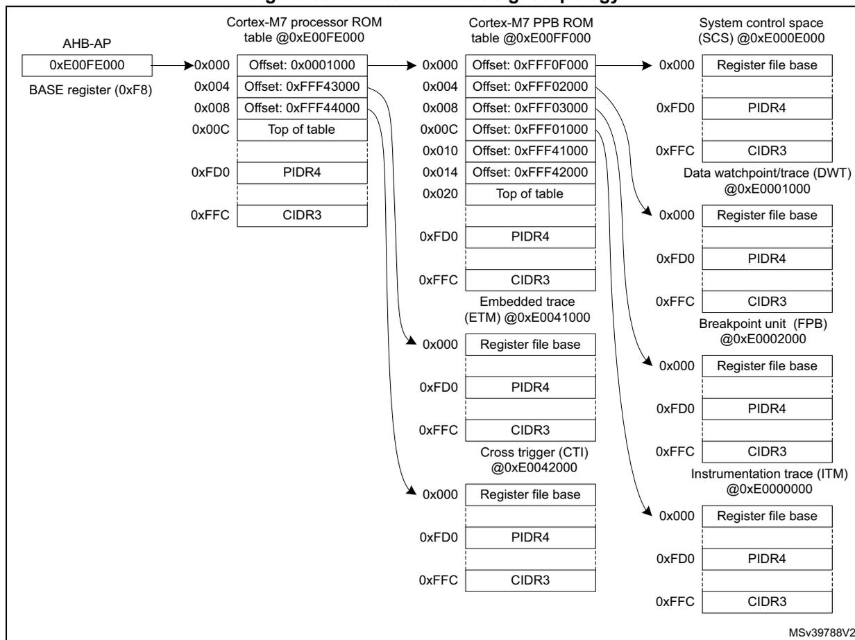
The diagram illustrates the CoreSight topology for Cortex-M7. It shows the following components and their connections:
- AHB-AP: Located at address 0xE00FE000. It contains a BASE register (0xF8). The BASE register points to the Cortex-M7 processor ROM table at address 0xE00FE000.
- Cortex-M7 processor ROM table @0xE00FE000: Contains entries for offsets 0x0001000, 0xFFF43000, and 0xFFF44000. The entry at 0x00C points to the top of the table. This table points to the Cortex-M7 PPB ROM table at address 0xE00FF000.
- Cortex-M7 PPB ROM table @0xE00FF000: Contains entries for offsets 0xFFF0F000, 0xFFF02000, 0xFFF03000, 0xFFF01000, 0xFFF41000, and 0xFFF42000. The entry at 0x020 points to the top of the table. This table points to the System control space (SCS) at address 0xE000E000.
- System control space (SCS) @0xE000E000:
Contains the following registers:
- 0x000: Register file base
- 0xFD0: PIDR4
- 0xFFC: CIDR3
- Data watchpoint/trace (DWT) @0xE0001000:
Contains the following registers:
- 0x000: Register file base
- 0xFD0: PIDR4
- 0xFFC: CIDR3
- Breakpoint unit (FPB) @0xE0002000:
Contains the following registers:
- 0x000: Register file base
- 0xFD0: PIDR4
- 0xFFC: CIDR3
- Instrumentation trace (ITM) @0xE0000000:
Contains the following registers:
- 0x000: Register file base
- 0xFD0: PIDR4
- 0xFFC: CIDR3
- Embedded trace (ETM) @0xE0041000:
Contains the following registers:
- 0x000: Register file base
- 0xFD0: PIDR4
- 0xFFC: CIDR3
- Cross trigger (CTI) @0xE0042000:
Contains the following registers:
- 0x000: Register file base
- 0xFD0: PIDR4
- 0xFFC: CIDR3
MSv39788V2
Cortex-M7 processor ROM registers
Processor ROM memory type register (M7_CPUROM_MEMTYPE)
Address offset: 0xFCC
Reset value: 0x0000 0001
| 31 | 30 | 29 | 28 | 27 | 26 | 25 | 24 | 23 | 22 | 21 | 20 | 19 | 18 | 17 | 16 |
|---|---|---|---|---|---|---|---|---|---|---|---|---|---|---|---|
| Res. | Res. | Res. | Res. | Res. | Res. | Res. | Res. | Res. | Res. | Res. | Res. | Res. | Res. | Res. | Res. |
| 15 | 14 | 13 | 12 | 11 | 10 | 9 | 8 | 7 | 6 | 5 | 4 | 3 | 2 | 1 | 0 |
| Res. | Res. | Res. | Res. | Res. | Res. | Res. | Res. | Res. | Res. | Res. | Res. | Res. | Res. | Res. | SYSME M |
| r |
Bits 31:1 Reserved, must be kept at reset value.
Bit 0 SYSMEM : System memory presence
1: System memory is present on this bus
Processor ROM CoreSight peripheral identity register 4 (M7_CPUROM_PIDR4)
Address offset: 0xFD0
Reset value: 0x0000 0004
| 31 | 30 | 29 | 28 | 27 | 26 | 25 | 24 | 23 | 22 | 21 | 20 | 19 | 18 | 17 | 16 |
|---|---|---|---|---|---|---|---|---|---|---|---|---|---|---|---|
| Res. | Res. | Res. | Res. | Res. | Res. | Res. | Res. | Res. | Res. | Res. | Res. | Res. | Res. | Res. | Res. |
| 15 | 14 | 13 | 12 | 11 | 10 | 9 | 8 | 7 | 6 | 5 | 4 | 3 | 2 | 1 | 0 |
| Res. | Res. | Res. | Res. | Res. | Res. | Res. | Res. | 4KCOUNT[3:0] | JEP106CON[3:0] | ||||||
| r | r | r | r | r | r | r | r | ||||||||
Bits 31:8 Reserved, must be kept at reset value.
Bits 7:4 4KCOUNT[3:0] : Register file size
0x0: Register file occupies a single 4 Kbyte region
Bits 3:0 JEP106CON[3:0] : JEP106 continuation code
0x4: Arm ® JEDEC continuation code
Processor ROM CoreSight peripheral identity register 0 (M7_CPUROM_PIDR0)
Address offset: 0xFE0
Reset value: 0x0000 0050
| 31 | 30 | 29 | 28 | 27 | 26 | 25 | 24 | 23 | 22 | 21 | 20 | 19 | 18 | 17 | 16 |
|---|---|---|---|---|---|---|---|---|---|---|---|---|---|---|---|
| Res. | Res. | Res. | Res. | Res. | Res. | Res. | Res. | Res. | Res. | Res. | Res. | Res. | Res. | Res. | Res. |
| 15 | 14 | 13 | 12 | 11 | 10 | 9 | 8 | 7 | 6 | 5 | 4 | 3 | 2 | 1 | 0 |
| Res. | Res. | Res. | Res. | Res. | Res. | Res. | Res. | PARTNUM[7:0] | |||||||
| r | r | r | r | r | r | r | r | ||||||||
Bits 31:8 Reserved, must be kept at reset value.
Bits 7:0 PARTNUM[7:0] : Part number field, bits [7:0]
0x50: STM32H7
Processor ROM CoreSight peripheral identity register 1
(M7_CPUROM_PIDR1)
Address offset: 0xFE4
Reset value: 0x0000 0004
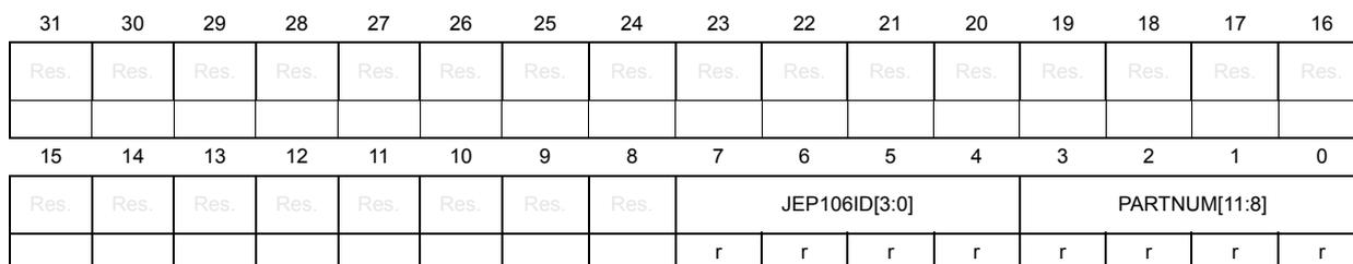
| 31 | 30 | 29 | 28 | 27 | 26 | 25 | 24 | 23 | 22 | 21 | 20 | 19 | 18 | 17 | 16 |
|---|---|---|---|---|---|---|---|---|---|---|---|---|---|---|---|
| Res. | Res. | Res. | Res. | Res. | Res. | Res. | Res. | Res. | Res. | Res. | Res. | Res. | Res. | Res. | Res. |
| 15 | 14 | 13 | 12 | 11 | 10 | 9 | 8 | 7 | 6 | 5 | 4 | 3 | 2 | 1 | 0 |
|---|---|---|---|---|---|---|---|---|---|---|---|---|---|---|---|
| Res. | Res. | Res. | Res. | Res. | Res. | Res. | Res. | JEP106ID[3:0] | PARTNUM[11:8] | ||||||
| r | r | r | r | r | r | r | r | ||||||||
Bits 31:8 Reserved, must be kept at reset value.
Bits 7:4 JEP106ID[3:0] : JEP106 identity code field, bits [3:0]
0x0: STMicroelectronics JEDEC code
Bits 3:0 PARTNUM[11:8] : Part number field, bits [11:8]
0x4: STM32H7
Processor ROM CoreSight peripheral identity register 2
(M7_CPUROM_PIDR2)
Address offset: 0xFE8
Reset value: 0x0000 000B
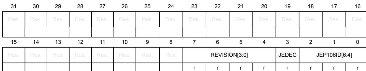
| 31 | 30 | 29 | 28 | 27 | 26 | 25 | 24 | 23 | 22 | 21 | 20 | 19 | 18 | 17 | 16 |
|---|---|---|---|---|---|---|---|---|---|---|---|---|---|---|---|
| Res. | Res. | Res. | Res. | Res. | Res. | Res. | Res. | Res. | Res. | Res. | Res. | Res. | Res. | Res. | Res. |
| 15 | 14 | 13 | 12 | 11 | 10 | 9 | 8 | 7 | 6 | 5 | 4 | 3 | 2 | 1 | 0 |
|---|---|---|---|---|---|---|---|---|---|---|---|---|---|---|---|
| Res. | Res. | Res. | Res. | Res. | Res. | Res. | Res. | REVISION[3:0] | JEDEC | JEP106ID[6:4] | |||||
| r | r | r | r | r | r | r | r | ||||||||
Bits 31:8 Reserved, must be kept at reset value.
Bits 7:4 REVISION[3:0] : Component revision number
0x0: rev 0
Bit 3 JEDEC : JEDEC assigned value
1: Designer ID specified by JEDEC
Bits 2:0 JEP106ID[6:4] : JEP106 identity code field, bits [6:4]
0x2: STMicroelectronics JEDEC code
Processor ROM CoreSight peripheral identity register 3 (M7_CPUROM_PIDR3)
Address offset: 0xFEC
Reset value: 0x0000 0000
| 31 | 30 | 29 | 28 | 27 | 26 | 25 | 24 | 23 | 22 | 21 | 20 | 19 | 18 | 17 | 16 |
|---|---|---|---|---|---|---|---|---|---|---|---|---|---|---|---|
| Res. | Res. | Res. | Res. | Res. | Res. | Res. | Res. | Res. | Res. | Res. | Res. | Res. | Res. | Res. | Res. |
| 15 | 14 | 13 | 12 | 11 | 10 | 9 | 8 | 7 | 6 | 5 | 4 | 3 | 2 | 1 | 0 |
| Res. | Res. | Res. | Res. | Res. | Res. | Res. | Res. | REVAND[3:0] | CMOD[3:0] | ||||||
| r | r | r | r | r | r | r | r | ||||||||
Bits 31:8 Reserved, must be kept at reset value.
Bits 7:4
REVAND[3:0]
: Metal fix version
0x0: No metal fix
Bits 3:0
CMOD[3:0]
: Customer modified
0x0: No customer modifications
Processor ROM CoreSight component identity register 0 (M7_CPUROM_CIDR0)
Address offset: 0xFF0
Reset value: 0x0000 000D
| 31 | 30 | 29 | 28 | 27 | 26 | 25 | 24 | 23 | 22 | 21 | 20 | 19 | 18 | 17 | 16 |
|---|---|---|---|---|---|---|---|---|---|---|---|---|---|---|---|
| Res. | Res. | Res. | Res. | Res. | Res. | Res. | Res. | Res. | Res. | Res. | Res. | Res. | Res. | Res. | Res. |
| 15 | 14 | 13 | 12 | 11 | 10 | 9 | 8 | 7 | 6 | 5 | 4 | 3 | 2 | 1 | 0 |
| Res. | Res. | Res. | Res. | Res. | Res. | Res. | Res. | PREAMBLE[7:0] | |||||||
| r | r | r | r | r | r | r | r | ||||||||
Bits 31:8 Reserved, must be kept at reset value.
Bits 7:0
PREAMBLE[7:0]
: Component ID field, bits [7:0]
0x0D: Common ID value
Processor ROM CoreSight component identity register 1
(M7_CPUROM_CIDR1)
Address offset: 0xFF4
Reset value: 0x0000 0010
| 31 | 30 | 29 | 28 | 27 | 26 | 25 | 24 | 23 | 22 | 21 | 20 | 19 | 18 | 17 | 16 |
|---|---|---|---|---|---|---|---|---|---|---|---|---|---|---|---|
| Res. | Res. | Res. | Res. | Res. | Res. | Res. | Res. | Res. | Res. | Res. | Res. | Res. | Res. | Res. | Res. |
| 15 | 14 | 13 | 12 | 11 | 10 | 9 | 8 | 7 | 6 | 5 | 4 | 3 | 2 | 1 | 0 |
| Res. | Res. | Res. | Res. | Res. | Res. | Res. | Res. | CLASS[3:0] | PREAMBLE[11:8] | ||||||
| r | r | r | r | r | r | r | r | ||||||||
Bits 31:8 Reserved, must be kept at reset value.
Bits 7:4
CLASS[3:0]
: Component ID field, bits [15:12] - component class
0x1: ROM table component
Bits 3:0
PREAMBLE[11:8]
: Component ID field, bits [11:8]
0x0: Common ID value
Processor ROM CoreSight component identity register 2
(M7_CPUROM_CIDR2)
Address offset: 0xFF8
Reset value: 0x0000 0005
| 31 | 30 | 29 | 28 | 27 | 26 | 25 | 24 | 23 | 22 | 21 | 20 | 19 | 18 | 17 | 16 |
|---|---|---|---|---|---|---|---|---|---|---|---|---|---|---|---|
| Res. | Res. | Res. | Res. | Res. | Res. | Res. | Res. | Res. | Res. | Res. | Res. | Res. | Res. | Res. | Res. |
| 15 | 14 | 13 | 12 | 11 | 10 | 9 | 8 | 7 | 6 | 5 | 4 | 3 | 2 | 1 | 0 |
| Res. | Res. | Res. | Res. | Res. | Res. | Res. | Res. | PREAMBLE[19:12] | |||||||
| r | r | r | r | r | r | r | r | ||||||||
Bits 31:8 Reserved, must be kept at reset value.
Bits 7:0
PREAMBLE[19:12]
: Component ID field, bits [23:16]
0x05: Common ID value
Processor ROM CoreSight component identity register 3 (M7_CPUROM_CIDR3)
Address offset: 0xFFC
Reset value: 0x0000 00B1
| 31 | 30 | 29 | 28 | 27 | 26 | 25 | 24 | 23 | 22 | 21 | 20 | 19 | 18 | 17 | 16 |
|---|---|---|---|---|---|---|---|---|---|---|---|---|---|---|---|
| Res. | Res. | Res. | Res. | Res. | Res. | Res. | Res. | Res. | Res. | Res. | Res. | Res. | Res. | Res. | Res. |
| 15 | 14 | 13 | 12 | 11 | 10 | 9 | 8 | 7 | 6 | 5 | 4 | 3 | 2 | 1 | 0 |
| Res. | Res. | Res. | Res. | Res. | Res. | Res. | Res. | PREAMBLE[27:20] | |||||||
| r | r | r | r | r | r | r | r | ||||||||
Bits 31:8 Reserved, must be kept at reset value.
Bits 7:0
PREAMBLE[27:20]
: Component ID field, bits [31:24]
0xB1: Common ID value
Cortex-M7 processor ROM table register map and reset values
Table 645. Cortex-M7 processor ROM table register map and reset values
| Offset | Register name | 31 | 30 | 29 | 28 | 27 | 26 | 25 | 24 | 23 | 22 | 21 | 20 | 19 | 18 | 17 | 16 | 15 | 14 | 13 | 12 | 11 | 10 | 9 | 8 | 7 | 6 | 5 | 4 | 3 | 2 | 1 | 0 |
|---|---|---|---|---|---|---|---|---|---|---|---|---|---|---|---|---|---|---|---|---|---|---|---|---|---|---|---|---|---|---|---|---|---|
| 0xFCC | M7_CPUROM_ MEMTYPE | Res. | Res. | Res. | Res. | Res. | Res. | Res. | Res. | Res. | Res. | Res. | Res. | Res. | Res. | Res. | Res. | Res. | Res. | Res. | Res. | Res. | Res. | Res. | Res. | Res. | Res. | Res. | Res. | Res. | Res. | Res. | SYSMEM |
| Reset value | 1 | ||||||||||||||||||||||||||||||||
| 0xFD0 | M7_CPUROM_ PIDR4 | Res. | Res. | Res. | Res. | Res. | Res. | Res. | Res. | Res. | Res. | Res. | Res. | Res. | Res. | Res. | Res. | Res. | Res. | Res. | Res. | Res. | Res. | Res. | Res. | 4KCOUNT[3:0] | JEP106CON[3:0] | ||||||
| Reset value | 0 | 0 | 0 | 0 | 0 | 0 | 0 | 0 | |||||||||||||||||||||||||
| 0xFD4 to 0xFDC | Reserved | Reserved | |||||||||||||||||||||||||||||||
| 0xFE0 | M7_CPUROM_ PIDR0 | Res. | Res. | Res. | Res. | Res. | Res. | Res. | Res. | Res. | Res. | Res. | Res. | Res. | Res. | Res. | Res. | Res. | Res. | Res. | Res. | Res. | Res. | Res. | Res. | PARTNUM[7:0] | |||||||
| Reset value | 0 | 1 | 0 | 1 | 0 | 0 | 0 | 0 | |||||||||||||||||||||||||
| 0xFE4 | M7_CPUROM_ PIDR1 | Res. | Res. | Res. | Res. | Res. | Res. | Res. | Res. | Res. | Res. | Res. | Res. | Res. | Res. | Res. | Res. | Res. | Res. | Res. | Res. | Res. | Res. | Res. | Res. | JEP106ID[3:0] | PARTNUM[11:8] | ||||||
| Reset value | 0 | 0 | 0 | 0 | 0 | 1 | 0 | 0 | |||||||||||||||||||||||||
| 0xFE8 | M7_CPUROM_ PIDR2 | Res. | Res. | Res. | Res. | Res. | Res. | Res. | Res. | Res. | Res. | Res. | Res. | Res. | Res. | Res. | Res. | Res. | Res. | Res. | Res. | Res. | Res. | Res. | Res. | REVISION[3:0] | JEDEC | JEP106ID[6:4] | |||||
| Reset value | 0 | 0 | 0 | 0 | 1 | 0 | 1 | 0 | |||||||||||||||||||||||||
| 0xFEC | M7_CPUROM_ PIDR3 | Res. | Res. | Res. | Res. | Res. | Res. | Res. | Res. | Res. | Res. | Res. | Res. | Res. | Res. | Res. | Res. | Res. | Res. | Res. | Res. | Res. | Res. | Res. | Res. | REVAND[3:0] | CMOD[3:0] | ||||||
| Reset value | 0 | 0 | 0 | 0 | 0 | 0 | 0 | 0 | |||||||||||||||||||||||||
| 0xFF0 | M7_CPUROM_ CIDR0 | Res. | Res. | Res. | Res. | Res. | Res. | Res. | Res. | Res. | Res. | Res. | Res. | Res. | Res. | Res. | Res. | Res. | Res. | Res. | Res. | Res. | Res. | Res. | Res. | PREAMBLE[7:0] | |||||||
| Reset value | 0 | 0 | 0 | 0 | 1 | 1 | 0 | 1 | |||||||||||||||||||||||||
| 0xFF4 | M7_CPUROM_ CIDR1 | Res. | Res. | Res. | Res. | Res. | Res. | Res. | Res. | Res. | Res. | Res. | Res. | Res. | Res. | Res. | Res. | Res. | Res. | Res. | Res. | Res. | Res. | Res. | Res. | CLASS[3:0] | PREAMBLE[11:8] | ||||||
| Reset value | 0 | 0 | 0 | 1 | 0 | 0 | 0 | 0 | |||||||||||||||||||||||||
Table 645. Cortex-M7 processor ROM table register map and reset values (continued)
| Offset | Register name | 31 | 30 | 29 | 28 | 27 | 26 | 25 | 24 | 23 | 22 | 21 | 20 | 19 | 18 | 17 | 16 | 15 | 14 | 13 | 12 | 11 | 10 | 9 | 8 | 7 | 6 | 5 | 4 | 3 | 2 | 1 | 0 |
|---|---|---|---|---|---|---|---|---|---|---|---|---|---|---|---|---|---|---|---|---|---|---|---|---|---|---|---|---|---|---|---|---|---|
| 0xFF8 | M7_CPUROM_ _CIDR2 | Res. | Res. | Res. | Res. | Res. | Res. | Res. | Res. | Res. | Res. | Res. | Res. | Res. | Res. | Res. | Res. | Res. | Res. | Res. | Res. | Res. | Res. | Res. | Res. | PREAMBLE[19:12] | |||||||
| Reset value | 0 | 0 | 0 | 0 | 0 | 1 | 0 | 1 | |||||||||||||||||||||||||
| 0xFFC | M7_CPUROM_ _CIDR3 | Res. | Res. | Res. | Res. | Res. | Res. | Res. | Res. | Res. | Res. | Res. | Res. | Res. | Res. | Res. | Res. | Res. | Res. | Res. | Res. | Res. | Res. | Res. | Res. | PREAMBLE[27:20] | |||||||
| Reset value | 1 | 0 | 1 | 1 | 0 | 0 | 0 | 1 | |||||||||||||||||||||||||
Cortex-M7 PPB ROM registers
PPB ROM memory type register (M7_PPBROM_MEMTYPE)
Address offset: 0xFCC
Reset value: 0x0000 0001
| 31 | 30 | 29 | 28 | 27 | 26 | 25 | 24 | 23 | 22 | 21 | 20 | 19 | 18 | 17 | 16 |
|---|---|---|---|---|---|---|---|---|---|---|---|---|---|---|---|
| Res. | Res. | Res. | Res. | Res. | Res. | Res. | Res. | Res. | Res. | Res. | Res. | Res. | Res. | Res. | Res. |
| 15 | 14 | 13 | 12 | 11 | 10 | 9 | 8 | 7 | 6 | 5 | 4 | 3 | 2 | 1 | 0 |
| Res. | Res. | Res. | Res. | Res. | Res. | Res. | Res. | Res. | Res. | Res. | Res. | Res. | Res. | Res. | SYSEM M |
| r |
Bits 31:1 Reserved, must be kept at reset value.
Bit 0 SYSEM : System memory presence
1: System memory is present on this bus
PPB ROM CoreSight peripheral identity register 4 (M7_PPBROM_PIDR4)
Address offset: 0xFD0
Reset value: 0x0000 0004
| 31 | 30 | 29 | 28 | 27 | 26 | 25 | 24 | 23 | 22 | 21 | 20 | 19 | 18 | 17 | 16 |
|---|---|---|---|---|---|---|---|---|---|---|---|---|---|---|---|
| Res. | Res. | Res. | Res. | Res. | Res. | Res. | Res. | Res. | Res. | Res. | Res. | Res. | Res. | Res. | Res. |
| 15 | 14 | 13 | 12 | 11 | 10 | 9 | 8 | 7 | 6 | 5 | 4 | 3 | 2 | 1 | 0 |
| Res. | Res. | Res. | Res. | Res. | Res. | Res. | Res. | 4KCOUNT[3:0] | JEP106CON[3:0] | ||||||
| r | r | r | r | r | r | r | r | ||||||||
Bits 31:8 Reserved, must be kept at reset value.
Bits 7:4 4KCOUNT[3:0] : Register file size
0x0: Register file occupies a single 4 Kbyte region
Bits 3:0 JEP106CON[3:0] : JEP106 continuation code
0x4: Arm ® JEDEC continuation code
PPB ROM CoreSight peripheral identity register 0 (M7_PPBROM_PIDR0)
Address offset: 0xFE0
Reset value: 0x0000 00C7
| 31 | 30 | 29 | 28 | 27 | 26 | 25 | 24 | 23 | 22 | 21 | 20 | 19 | 18 | 17 | 16 |
|---|---|---|---|---|---|---|---|---|---|---|---|---|---|---|---|
| Res. | Res. | Res. | Res. | Res. | Res. | Res. | Res. | Res. | Res. | Res. | Res. | Res. | Res. | Res. | Res. |
| 15 | 14 | 13 | 12 | 11 | 10 | 9 | 8 | 7 | 6 | 5 | 4 | 3 | 2 | 1 | 0 |
| Res. | Res. | Res. | Res. | Res. | Res. | Res. | Res. | PARTNUM[7:0] | |||||||
| r | r | r | r | r | r | r | r | ||||||||
Bits 31:8 Reserved, must be kept at reset value.
Bits 7:0 PARTNUM[7:0] : Part number field, bits [7:0]
0xC7: Cortex-M7 PPB ROM table
PPB ROM CoreSight peripheral identity register 1 (M7_PPBROM_PIDR1)
Address offset: 0xFE4
Reset value: 0x0000 00B0
| 31 | 30 | 29 | 28 | 27 | 26 | 25 | 24 | 23 | 22 | 21 | 20 | 19 | 18 | 17 | 16 |
|---|---|---|---|---|---|---|---|---|---|---|---|---|---|---|---|
| Res. | Res. | Res. | Res. | Res. | Res. | Res. | Res. | Res. | Res. | Res. | Res. | Res. | Res. | Res. | Res. |
| 15 | 14 | 13 | 12 | 11 | 10 | 9 | 8 | 7 | 6 | 5 | 4 | 3 | 2 | 1 | 0 |
| Res. | Res. | Res. | Res. | Res. | Res. | Res. | Res. | JEP106ID[3:0] | PARTNUM[11:8] | ||||||
| r | r | r | r | r | r | r | r | ||||||||
Bits 31:8 Reserved, must be kept at reset value.
Bits 7:4 JEP106ID[3:0] : JEP106 identity code field, bits [3:0]
0xB: Arm ® JEDEC code
Bits 3:0 PARTNUM[11:8] : Part number field, bits [11:8]
0x4: Cortex-M7 PPB ROM table
PPB ROM CoreSight peripheral identity register 2 (M7_PPBROM_PIDR2)
Address offset: 0xFE8
Reset value: 0x0000 000B
| 31 | 30 | 29 | 28 | 27 | 26 | 25 | 24 | 23 | 22 | 21 | 20 | 19 | 18 | 17 | 16 |
|---|---|---|---|---|---|---|---|---|---|---|---|---|---|---|---|
| Res. | Res. | Res. | Res. | Res. | Res. | Res. | Res. | Res. | Res. | Res. | Res. | Res. | Res. | Res. | Res. |
| 15 | 14 | 13 | 12 | 11 | 10 | 9 | 8 | 7 | 6 | 5 | 4 | 3 | 2 | 1 | 0 |
| Res. | Res. | Res. | Res. | Res. | Res. | Res. | Res. | REVISION[3:0] | JEDEC | JEP106ID[6:4] | |||||
| r | r | r | r | r | r | r | r | ||||||||
Bits 31:8 Reserved, must be kept at reset value.
Bits 7:4 REVISION[3:0] : Component revision number
0x0: rev r0p0
Bit 3 JEDEC : JEDEC assigned value
1: Designer ID specified by JEDEC
Bits 2:0 JEP106ID[6:4] : JEP106 identity code field, bits [6:4]
0x3: Arm ® JEDEC code
PPB ROM CoreSight peripheral identity register 3 (M7_PPBROM_PIDR3)
Address offset: 0xFEC
Reset value: 0x0000 0000
| 31 | 30 | 29 | 28 | 27 | 26 | 25 | 24 | 23 | 22 | 21 | 20 | 19 | 18 | 17 | 16 |
|---|---|---|---|---|---|---|---|---|---|---|---|---|---|---|---|
| Res. | Res. | Res. | Res. | Res. | Res. | Res. | Res. | Res. | Res. | Res. | Res. | Res. | Res. | Res. | Res. |
| 15 | 14 | 13 | 12 | 11 | 10 | 9 | 8 | 7 | 6 | 5 | 4 | 3 | 2 | 1 | 0 |
| Res. | Res. | Res. | Res. | Res. | Res. | Res. | Res. | REVAND[3:0] | CMOD[3:0] | ||||||
| r | r | r | r | r | r | r | r | ||||||||
Bits 31:8 Reserved, must be kept at reset value.
Bits 7:4 REVAND[3:0] : Metal fix version
0x0: No metal fix
Bits 3:0 CMOD[3:0] : Customer modified
0x0: No customer modifications
PPB ROM CoreSight component identity register 0 (M7_PPBROM_CIDR0)
Address offset: 0xFF0
Reset value: 0x0000 000D
| 31 | 30 | 29 | 28 | 27 | 26 | 25 | 24 | 23 | 22 | 21 | 20 | 19 | 18 | 17 | 16 |
|---|---|---|---|---|---|---|---|---|---|---|---|---|---|---|---|
| Res. | Res. | Res. | Res. | Res. | Res. | Res. | Res. | Res. | Res. | Res. | Res. | Res. | Res. | Res. | Res. |
| 15 | 14 | 13 | 12 | 11 | 10 | 9 | 8 | 7 | 6 | 5 | 4 | 3 | 2 | 1 | 0 |
| Res. | Res. | Res. | Res. | Res. | Res. | Res. | Res. | PREAMBLE[7:0] | |||||||
| r | r | r | r | r | r | r | r | ||||||||
Bits 31:8 Reserved, must be kept at reset value.
Bits 7:0 PREAMBLE[7:0] : Component ID field, bits [7:0]
0x0D: Common ID value
PPB ROM CoreSight component identity register 1 (M7_PPBROM_CIDR1)
Address offset: 0xFF4
Reset value: 0x0000 0010
| 31 | 30 | 29 | 28 | 27 | 26 | 25 | 24 | 23 | 22 | 21 | 20 | 19 | 18 | 17 | 16 |
|---|---|---|---|---|---|---|---|---|---|---|---|---|---|---|---|
| Res. | Res. | Res. | Res. | Res. | Res. | Res. | Res. | Res. | Res. | Res. | Res. | Res. | Res. | Res. | Res. |
| 15 | 14 | 13 | 12 | 11 | 10 | 9 | 8 | 7 | 6 | 5 | 4 | 3 | 2 | 1 | 0 |
| Res. | Res. | Res. | Res. | Res. | Res. | Res. | Res. | CLASS[3:0] | PREAMBLE[11:8] | ||||||
| r | r | r | r | r | r | r | r | ||||||||
Bits 31:8 Reserved, must be kept at reset value.
Bits 7:4 CLASS[3:0] : Component ID field, bits [15:12] - component class
0x1: ROM table component
Bits 3:0 PREAMBLE[11:8] : Component ID field, bits [11:8]
0x0: Common ID value
PPB ROM CoreSight component identity register 2 (M7_PPBROM_CIDR2)
Address offset: 0xFF8
Reset value: 0x0000 0005
| 31 | 30 | 29 | 28 | 27 | 26 | 25 | 24 | 23 | 22 | 21 | 20 | 19 | 18 | 17 | 16 |
|---|---|---|---|---|---|---|---|---|---|---|---|---|---|---|---|
| Res. | Res. | Res. | Res. | Res. | Res. | Res. | Res. | Res. | Res. | Res. | Res. | Res. | Res. | Res. | Res. |
| 15 | 14 | 13 | 12 | 11 | 10 | 9 | 8 | 7 | 6 | 5 | 4 | 3 | 2 | 1 | 0 |
| Res. | Res. | Res. | Res. | Res. | Res. | Res. | Res. | PREAMBLE[19:12] | |||||||
| r | r | r | r | r | r | r | r | ||||||||
Bits 31:8 Reserved, must be kept at reset value.
Bits 7:0 PREAMBLE[19:12] : Component ID field, bits [23:16]
0x05: Common ID value
PPB ROM CoreSight component identity register 3 (M7_PPBROM_CIDR3)
Address offset: 0xFFC
Reset value: 0x0000 00B1
| 31 | 30 | 29 | 28 | 27 | 26 | 25 | 24 | 23 | 22 | 21 | 20 | 19 | 18 | 17 | 16 |
|---|---|---|---|---|---|---|---|---|---|---|---|---|---|---|---|
| Res. | Res. | Res. | Res. | Res. | Res. | Res. | Res. | Res. | Res. | Res. | Res. | Res. | Res. | Res. | Res. |
| 15 | 14 | 13 | 12 | 11 | 10 | 9 | 8 | 7 | 6 | 5 | 4 | 3 | 2 | 1 | 0 |
| Res. | Res. | Res. | Res. | Res. | Res. | Res. | Res. | PREAMBLE[27:20] | |||||||
| r | r | r | r | r | r | r | r | ||||||||
Bits 31:8 Reserved, must be kept at reset value.
Bits 7:0 PREAMBLE[27:20] : Component ID field, bits [31:24]
0xB1: Common ID value
Cortex-M7 PPB ROM table register map and reset values
Table 646. Cortex-M7 PPB ROM table register map and reset values
| Offset | Register name | 31 | 30 | 29 | 28 | 27 | 26 | 25 | 24 | 23 | 22 | 21 | 20 | 19 | 18 | 17 | 16 | 15 | 14 | 13 | 12 | 11 | 10 | 9 | 8 | 7 | 6 | 5 | 4 | 3 | 2 | 1 | 0 |
|---|---|---|---|---|---|---|---|---|---|---|---|---|---|---|---|---|---|---|---|---|---|---|---|---|---|---|---|---|---|---|---|---|---|
| 0xFFC | M7_PPBROM_ _MEMTYPE | Res. | Res. | Res. | Res. | Res. | Res. | Res. | Res. | Res. | Res. | Res. | Res. | Res. | Res. | Res. | Res. | Res. | Res. | Res. | Res. | Res. | Res. | Res. | Res. | Res. | Res. | Res. | Res. | Res. | Res. | Res. | SYSTEMMEM |
| Reset value | 1 | ||||||||||||||||||||||||||||||||
| 0xFF0 | M7_PPBROM_ _PIDR4 | Res. | Res. | Res. | Res. | Res. | Res. | Res. | Res. | Res. | Res. | Res. | Res. | Res. | Res. | Res. | Res. | Res. | Res. | Res. | Res. | Res. | Res. | Res. | Res. | Res. | 4KCOUNT[3: 0] | JEP106CON[ 3:0] | |||||
| Reset value | 0 | 0 | 0 | 0 | 0 | 1 | 0 | 0 | |||||||||||||||||||||||||
| 0xFF4 to 0xFFC | Reserved | Reserved | |||||||||||||||||||||||||||||||
Table 646. Cortex-M7 PPB ROM table register map and reset values (continued)
| Offset | Register name | 31 | 30 | 29 | 28 | 27 | 26 | 25 | 24 | 23 | 22 | 21 | 20 | 19 | 18 | 17 | 16 | 15 | 14 | 13 | 12 | 11 | 10 | 9 | 8 | 7 | 6 | 5 | 4 | 3 | 2 | 1 | 0 | |
|---|---|---|---|---|---|---|---|---|---|---|---|---|---|---|---|---|---|---|---|---|---|---|---|---|---|---|---|---|---|---|---|---|---|---|
| 0xFE0 | M7_PPBROM_PIDR0 | Res. | Res. | Res. | Res. | Res. | Res. | Res. | Res. | Res. | Res. | Res. | Res. | Res. | Res. | Res. | Res. | Res. | Res. | Res. | Res. | Res. | Res. | Res. | Res. | PARTNUM[7:0] | ||||||||
| Reset value | 1 | 1 | 0 | 0 | 0 | 1 | 1 | 1 | 1 | |||||||||||||||||||||||||
| 0xFE4 | M7_PPBROM_PIDR1 | Res. | Res. | Res. | Res. | Res. | Res. | Res. | Res. | Res. | Res. | Res. | Res. | Res. | Res. | Res. | Res. | Res. | Res. | Res. | Res. | Res. | Res. | Res. | Res. | JEP106ID[3:0] | PARTNUM[11:8] | |||||||
| Reset value | 1 | 0 | 1 | 1 | 0 | 1 | 0 | 0 | 0 | |||||||||||||||||||||||||
| 0xFE8 | M7_PPBROM_PIDR2 | Res. | Res. | Res. | Res. | Res. | Res. | Res. | Res. | Res. | Res. | Res. | Res. | Res. | Res. | Res. | Res. | Res. | Res. | Res. | Res. | Res. | Res. | Res. | Res. | REVISION[3:0] | JEDDEC | JEP106ID[6:4] | ||||||
| Reset value | 0 | 0 | 0 | 0 | 1 | 0 | 1 | 1 | 1 | |||||||||||||||||||||||||
| 0xFEC | M7_PPBROM_PIDR3 | Res. | Res. | Res. | Res. | Res. | Res. | Res. | Res. | Res. | Res. | Res. | Res. | Res. | Res. | Res. | Res. | Res. | Res. | Res. | Res. | Res. | Res. | Res. | Res. | REVAND[3:0] | CMOD[3:0] | |||||||
| Reset value | 0 | 0 | 0 | 0 | 0 | 0 | 0 | 0 | 0 | |||||||||||||||||||||||||
| 0xFF0 | M7_PPBROM_CIDR0 | Res. | Res. | Res. | Res. | Res. | Res. | Res. | Res. | Res. | Res. | Res. | Res. | Res. | Res. | Res. | Res. | Res. | Res. | Res. | Res. | Res. | Res. | Res. | PREAMBLE[7:0] | |||||||||
| Reset value | 0 | 0 | 0 | 0 | 1 | 1 | 1 | 0 | 1 | |||||||||||||||||||||||||
| 0xFF4 | M7_PPBROM_CIDR1 | Res. | Res. | Res. | Res. | Res. | Res. | Res. | Res. | Res. | Res. | Res. | Res. | Res. | Res. | Res. | Res. | Res. | Res. | Res. | Res. | Res. | Res. | Res. | CLASS[3:0] | PREAMBLE[11:8] | ||||||||
| Reset value | 0 | 0 | 0 | 1 | 0 | 0 | 0 | 0 | 0 | |||||||||||||||||||||||||
| 0xFF8 | M7_PPBROM_CIDR2 | Res. | Res. | Res. | Res. | Res. | Res. | Res. | Res. | Res. | Res. | Res. | Res. | Res. | Res. | Res. | Res. | Res. | Res. | Res. | Res. | Res. | Res. | Res. | PREAMBLE[19:12] | |||||||||
| Reset value | 0 | 0 | 0 | 0 | 0 | 1 | 0 | 1 | 1 | |||||||||||||||||||||||||
| 0xFFC | M7_PPBROM_CIDR3 | Res. | Res. | Res. | Res. | Res. | Res. | Res. | Res. | Res. | Res. | Res. | Res. | Res. | Res. | Res. | Res. | Res. | Res. | Res. | Res. | Res. | Res. | Res. | PREAMBLE[27:20] | |||||||||
| Reset value | 1 | 0 | 1 | 1 | 1 | 0 | 0 | 0 | 1 | |||||||||||||||||||||||||
63.6.2 Cortex-M7 data watchpoint and trace unit (DWT)
The DWT provides four comparators that can be used as:
- • watchpoint
- • ETM trigger
- • PC sampling trigger
- • data address sampling trigger
- • data comparator (comparator 1 only)
- • clock cycle counter comparator (comparator 0 only)
It also contains counters for:
- • clock cycles
- • folded instructions
- • load store unit (LSU) operations
- • sleep cycles
- • number of cycles per instruction
- • interrupt overhead
A DWT comparator compares one of the following with the value held in its DWT_COMP register:
- • a data address
- • an instruction address
- • a data value
- • the cycle count value, for comparator 0 only.
For address matching, the comparator can use a mask, so it matches a range of addresses.
On a successful match, the comparator generates one of the following:
- • one or more DWT data trace packets, containing one or more of:
- – the address of the instruction that caused a data access
- – an address offset, bits[15:0] of the data access address
- – the matched data value
- • a watchpoint debug event, on either the PC value or the accessed data address
- • a CMPMATCH[N] event that signals the match outside the DWT unit
A watchpoint debug event either generates a DebugMonitor exception, or causes the processor to halt execution and enter Debug state.
For more details on how to use the DWT, refer to the Arm ® v7-M Architecture Reference Manual [5] .
Cortex-M7 DWT registers
DWT control register (M7_DWT_CTRL)
Address offset: 0x000
Reset value: 0x4000 0000
| 31 | 30 | 29 | 28 | 27 | 26 | 25 | 24 | 23 | 22 | 21 | 20 | 19 | 18 | 17 | 16 |
|---|---|---|---|---|---|---|---|---|---|---|---|---|---|---|---|
| NUMCOMP[3:0] | NOTR CPKT | NOEX TTRIG | NOCYC CNT | NOPRF CNT | Res. | CYCEV TENA | FOLDE VTENA | LSUEV TENA | SLEEP EVTEN A | EXCEV TENA | CPIEVT ENA | EXCTR CENA | |||
| r | r | r | r | r | r | r | r | rw | rw | rw | rw | rw | rw | rw | |
| 15 | 14 | 13 | 12 | 11 | 10 | 9 | 8 | 7 | 6 | 5 | 4 | 3 | 2 | 1 | 0 |
| Res. | Res. | Res. | PCSA MPLE NA | SYNCTAP[1:0] | CYCTA P | POSTINIT[3:0] | POSTRESET[3:0] | CYCCN TENA | |||||||
| rw | rw | rw | rw | rw | rw | rw | rw | rw | rw | rw | rw | rw | |||
Bits 31:28 NUMCOMP[3:0] : Number of comparators implemented (read-only)
0x4: Four comparators
Bit 27 NOTRCPKT : Trace sampling and exception tracing support (read-only)
0: Supported
Bit 26 NOEXTTRIG : External match signal, CMPMATCH support (read-only)
0: Supported
Bit 25 NOCYCCNT : Cycle counter support (read-only)
0: Supported
- Bit 24
NOPRFCNT
: Profiling counter support (read-only)
0: Supported - Bit 23 Reserved, must be kept at reset value.
- Bit 22
CYCEVTENA
: POSTCNT underflow event counter packet generation enable
0: Disabled
1: Enabled - Bit 21
FOLDEVVTENA
: Folded instruction counter overflow event generation enable
0: Disabled
1: Enabled - Bit 20
LSUEVTENA
: LSU counter overflow event generation enable
0: Disabled
1: Enabled - Bit 19
SLEEPEVTENA
: Sleep counter overflow event generation enable
0: Disabled
1: Enabled - Bit 18
EXCEVTENA
: Exception overhead counter overflow event generation enable
0: Disabled
1: Enabled - Bit 17
CPIEVTENA
: CPI counter overflow event generation enable
0: Disabled
1: Enabled - Bit 16
EXCTRCENA
: Exception trace generation enable
0: Disabled
1: Enabled - Bits 15:13 Reserved, must be kept at reset value.
- Bit 12
PCSAMPLENA
: POSTCNT counter use enable
Enables use of POSTCNT counter as a timer for Periodic PC sample packet generation.
0: Disabled
1: Enabled - Bits 11:10
SYNCTAP[1:0]
: Position of synchronization packet counter tap on CYCCNT counter
This selection determines the synchronization packet rate.
0x0: Disabled - no synchronization packets
0x1: Tap at CYCCNT[24]
0x2: Tap at CYCCNT[26]
0x3: Tap at CYCCNT[28] - Bit 9
CYCTAP
: Position of the POSTCNT tap on the CYCCNT counter
0: Tap at CYCCNT[6]
1: Tap at CYCCNT[10]
Bits 8:5 POSTINIT[3:0] : Initial value of the POSTCNT counter
Writes to this field are ignored if POSTCNT counter is enabled (that is, CYCEVTENA or PCSAMPLENA must be reset prior to writing POSTINIT).
Bits 4:1 POSTRESET[3:0] : Reload value of the POSTCNT counter.
Bit 0 CYCCNTENA : CYCCNT counter enable
0: Disabled
1: Enabled
DWT cycle count register (M7_DWT_CYCCNT)
Address offset: 0x004
Reset value: 0x0000 0000
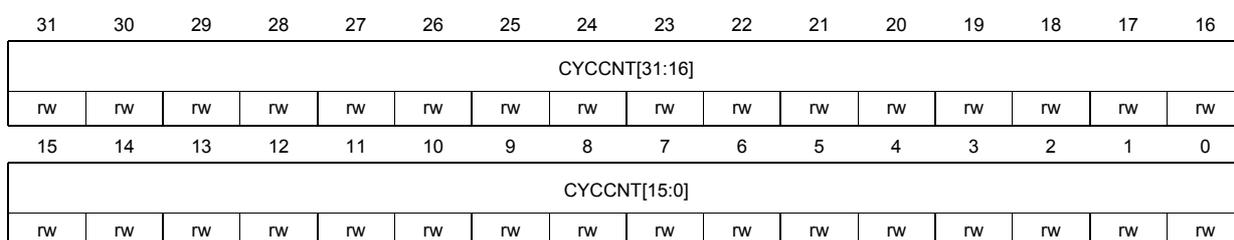
| 31 | 30 | 29 | 28 | 27 | 26 | 25 | 24 | 23 | 22 | 21 | 20 | 19 | 18 | 17 | 16 |
| CYCCNT[31:16] | |||||||||||||||
| rw | rw | rw | rw | rw | rw | rw | rw | rw | rw | rw | rw | rw | rw | rw | rw |
| 15 | 14 | 13 | 12 | 11 | 10 | 9 | 8 | 7 | 6 | 5 | 4 | 3 | 2 | 1 | 0 |
| CYCCNT[15:0] | |||||||||||||||
| rw | rw | rw | rw | rw | rw | rw | rw | rw | rw | rw | rw | rw | rw | rw | rw |
Bits 31:0 CYCCNT[31:0] : Processor clock cycle counter
DWT CPI count register (M7_DWT_CPICNT)
Address offset: 0x008
Reset value: 0x0000 0000
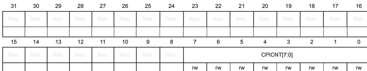
| 31 | 30 | 29 | 28 | 27 | 26 | 25 | 24 | 23 | 22 | 21 | 20 | 19 | 18 | 17 | 16 |
| Res. | Res. | Res. | Res. | Res. | Res. | Res. | Res. | Res. | Res. | Res. | Res. | Res. | Res. | Res. | Res. |
| 15 | 14 | 13 | 12 | 11 | 10 | 9 | 8 | 7 | 6 | 5 | 4 | 3 | 2 | 1 | 0 |
| Res. | Res. | Res. | Res. | Res. | Res. | Res. | Res. | CPICNT[7:0] | |||||||
| rw | rw | rw | rw | rw | rw | rw | rw | ||||||||
Bits 31:8 Reserved, must be kept at reset value.
Bits 7:0 CPICNT[7:0] : CPI counter
Counts additional cycles required to execute multi-cycle instructions, except those recorded by DWT_LSUCNT, and counts any instruction fetch stalls.
DWT exception count register (M7_DWT_EXCCNT)Address offset: 0x00C
Reset value: 0x0000 0000
| 31 | 30 | 29 | 28 | 27 | 26 | 25 | 24 | 23 | 22 | 21 | 20 | 19 | 18 | 17 | 16 |
|---|---|---|---|---|---|---|---|---|---|---|---|---|---|---|---|
| Res. | Res. | Res. | Res. | Res. | Res. | Res. | Res. | Res. | Res. | Res. | Res. | Res. | Res. | Res. | Res. |
| 15 | 14 | 13 | 12 | 11 | 10 | 9 | 8 | 7 | 6 | 5 | 4 | 3 | 2 | 1 | 0 |
| Res. | Res. | Res. | Res. | Res. | Res. | Res. | Res. | ||||||||
| rw | rw | rw | rw | rw | rw | rw | rw | ||||||||
| EXCCNT[7:0] | |||||||||||||||
Bits 31:8 Reserved, must be kept at reset value.
Bits 7:0 EXCCNT[7:0] : Exception overhead cycle counterCounts the number of cycles spent in exception processing.
DWT sleep count register (M7_DWT_SLP CNT)Address offset: 0x010
Reset value: 0x0000 0000
| 31 | 30 | 29 | 28 | 27 | 26 | 25 | 24 | 23 | 22 | 21 | 20 | 19 | 18 | 17 | 16 |
|---|---|---|---|---|---|---|---|---|---|---|---|---|---|---|---|
| Res. | Res. | Res. | Res. | Res. | Res. | Res. | Res. | Res. | Res. | Res. | Res. | Res. | Res. | Res. | Res. |
| 15 | 14 | 13 | 12 | 11 | 10 | 9 | 8 | 7 | 6 | 5 | 4 | 3 | 2 | 1 | 0 |
| Res. | Res. | Res. | Res. | Res. | Res. | Res. | Res. | ||||||||
| rw | rw | rw | rw | rw | rw | rw | rw | ||||||||
| SLP CNT[7:0] | |||||||||||||||
Bits 31:8 Reserved, must be kept at reset value.
Bits 7:0 SLP CNT[7:0] : Sleep cycle counterCounts the number of cycles spent in sleep mode (WFI, WFE, sleep-on-exit).
DWT LSU count register (M7_DWT_LSUCNT)Address offset: 0x014
Reset value: 0x0000 0000
| 31 | 30 | 29 | 28 | 27 | 26 | 25 | 24 | 23 | 22 | 21 | 20 | 19 | 18 | 17 | 16 |
|---|---|---|---|---|---|---|---|---|---|---|---|---|---|---|---|
| Res. | Res. | Res. | Res. | Res. | Res. | Res. | Res. | Res. | Res. | Res. | Res. | Res. | Res. | Res. | Res. |
| 15 | 14 | 13 | 12 | 11 | 10 | 9 | 8 | 7 | 6 | 5 | 4 | 3 | 2 | 1 | 0 |
| Res. | Res. | Res. | Res. | Res. | Res. | Res. | Res. | ||||||||
| rw | rw | rw | rw | rw | rw | rw | rw | ||||||||
| LSUCNT[7:0] | |||||||||||||||
Bits 31:8 Reserved, must be kept at reset value.
Bits 7:0 LSUCNT[7:0] : Load store counter
Counts additional cycles required to execute load and store instructions.
DWT fold count register (M7_DWT_FOLDCNT)
Address offset: 0x018
Reset value: 0x0000 0000
| 31 | 30 | 29 | 28 | 27 | 26 | 25 | 24 | 23 | 22 | 21 | 20 | 19 | 18 | 17 | 16 |
|---|---|---|---|---|---|---|---|---|---|---|---|---|---|---|---|
| Res. | Res. | Res. | Res. | Res. | Res. | Res. | Res. | Res. | Res. | Res. | Res. | Res. | Res. | Res. | Res. |
| 15 | 14 | 13 | 12 | 11 | 10 | 9 | 8 | 7 | 6 | 5 | 4 | 3 | 2 | 1 | 0 |
| Res. | Res. | Res. | Res. | Res. | Res. | Res. | Res. | FOLDCNT[7:0] | |||||||
| rw | rw | rw | rw | rw | rw | rw | rw | ||||||||
Bits 31:8 Reserved, must be kept at reset value.
Bits 7:0 FOLDCNT[7:0] : Folded instruction counter
Increments on each instruction that takes 0 cycles.
DWT program counter sample register (M7_DWT_PCSR)
Address offset: 0x01C
Reset value: 0x0000 0000
| 31 | 30 | 29 | 28 | 27 | 26 | 25 | 24 | 23 | 22 | 21 | 20 | 19 | 18 | 17 | 16 |
|---|---|---|---|---|---|---|---|---|---|---|---|---|---|---|---|
| EIASAMPLE[31:16] | |||||||||||||||
| rw | rw | rw | rw | rw | rw | rw | rw | rw | rw | rw | rw | rw | rw | rw | rw |
| 15 | 14 | 13 | 12 | 11 | 10 | 9 | 8 | 7 | 6 | 5 | 4 | 3 | 2 | 1 | 0 |
| EIASAMPLE[15:0] | |||||||||||||||
| rw | rw | rw | rw | rw | rw | rw | rw | rw | rw | rw | rw | rw | rw | rw | rw |
Bits 31:0 EIASAMPLE[31:0] : Executed instruction address sample value
Samples the current value of the program counter.
DWT comparator register x (M7_DWT_COMPx)
Address offset: 0x020 + x * 0x10 (for x = 0 to 3)
Reset value: 0x0000 0000
| 31 | 30 | 29 | 28 | 27 | 26 | 25 | 24 | 23 | 22 | 21 | 20 | 19 | 18 | 17 | 16 |
|---|---|---|---|---|---|---|---|---|---|---|---|---|---|---|---|
| COMP[31:16] | |||||||||||||||
| rw | rw | rw | rw | rw | rw | rw | rw | rw | rw | rw | rw | rw | rw | rw | rw |
| 15 | 14 | 13 | 12 | 11 | 10 | 9 | 8 | 7 | 6 | 5 | 4 | 3 | 2 | 1 | 0 |
|---|---|---|---|---|---|---|---|---|---|---|---|---|---|---|---|
| COMP[15:0] | |||||||||||||||
| rw | rw | rw | rw | rw | rw | rw | rw | rw | rw | rw | rw | rw | rw | rw | rw |
Bits 31:0 COMP[31:0] : Reference value for comparison.
DWT mask register x (M7_DWT_MASKx)
Address offset: 0x024 + x * 0x10 (for x = 0 to 3)
Reset value: 0x0000 0000
| 31 | 30 | 29 | 28 | 27 | 26 | 25 | 24 | 23 | 22 | 21 | 20 | 19 | 18 | 17 | 16 |
|---|---|---|---|---|---|---|---|---|---|---|---|---|---|---|---|
| Res. | Res. | Res. | Res. | Res. | Res. | Res. | Res. | Res. | Res. | Res. | Res. | Res. | Res. | Res. | Res. |
| 15 | 14 | 13 | 12 | 11 | 10 | 9 | 8 | 7 | 6 | 5 | 4 | 3 | 2 | 1 | 0 |
| Res. | Res. | Res. | Res. | Res. | Res. | Res. | Res. | Res. | Res. | Res. | MASK[4:0] | ||||
| rw | rw | rw | rw | rw | |||||||||||
Bits 31:5 Reserved, must be kept at reset value.
Bits 4:0 MASK[4:0] : Comparator mask size
Provides the size of the ignore mask applied to the access address for address range matching by comparator n. A debugger can write 0b11111 to this field and then read the register back to determine the maximum mask size supported.
DWT function register x (M7_DWT_FUNCTx)
Address offset: 0x028 + x * 0x10 (for x = 0 to 3)
Reset value: 0x0000 0000
| 31 | 30 | 29 | 28 | 27 | 26 | 25 | 24 | 23 | 22 | 21 | 20 | 19 | 18 | 17 | 16 |
|---|---|---|---|---|---|---|---|---|---|---|---|---|---|---|---|
| Res. | Res. | Res. | Res. | Res. | Res. | Res. | MATCHED | Res. | Res. | Res. | Res. | DATAVADDR1[3:0] | |||
| r | rw | rw | rw | rw | |||||||||||
| 15 | 14 | 13 | 12 | 11 | 10 | 9 | 8 | 7 | 6 | 5 | 4 | 3 | 2 | 1 | 0 |
| DATAVADDR0[3:0] | DATAVSIZE[1:0] | LINK1ENA | DATAVMATCH | CYCMATCH | Res. | EMITRANGE | Res. | FUNCTION[3:0] | |||||||
| rw | rw | rw | rw | rw | rw | rw | rw | rw | rw | rw | rw | rw | rw | ||
Bits 31:25 Reserved, must be kept at reset value.
Bit 24 MATCHED : Comparator match (read-only)
Indicates if a comparator match has occurred since the register was last read.
0: No match
1: Match occurred
Bits 23:20 Reserved, must be kept at reset value.
Bits 19:16 DATAVADDR1[3:0] : Comparator number of a second comparator
When the DATAVMATCH and LNK1ENA bits are both 1, this field can hold the comparator number of a second comparator to use for linked address comparison.
Bits 15:12 DATAVADDR0[3:0] : Comparator number of a comparator
When the DATAVMATCH and LNK1ENA bits are both 1, this field can hold the comparator number of a comparator to use for linked address comparison.
Bits 11:10 DATAVSIZE[1:0] : Size of required data comparison
For data value matching, specifies the size of the required data comparison.
0x0: Byte
0x1: Half word
0x2: Word
0x3: Reserved
Bit 9 LNK1ENA : Support of a second linked comparator (read-only)
Indicates whether the use of a second linked comparator is supported (read-only).
1: Supported
Bit 8 DATAVMATCH : Cycle comparison enable
0: Perform address comparison
1: Perform data value comparison
Bit 7 CYCMATCH : Cycle count comparison enable on comparator 0
This field is reserved for other comparators.
0: No cycle count comparison
1: Compare DWT_COMP0 with the cycle counter, DWT_CYCCNT
Bit 6 Reserved, must be kept at reset value.
Bit 5 EMITRANGE : Data trace address offset packet enable
Enables generation of data trace address offset packets (containing data address bits 0 to 15)
0: Disabled
1: Enabled
Bit 4 Reserved, must be kept at reset value.
Bits 3:0 FUNCTION[3:0] : Action on comparator match
The meaning of this bit field depends on the setting of the DATAVMATCH and CYCMATCH fields. See [5].
DWT CoreSight peripheral identity register 4 (M7_DWT_PIDR4)
Address offset: 0xFD0
Reset value: 0x0000 0004
| 31 | 30 | 29 | 28 | 27 | 26 | 25 | 24 | 23 | 22 | 21 | 20 | 19 | 18 | 17 | 16 |
|---|---|---|---|---|---|---|---|---|---|---|---|---|---|---|---|
| Res. | Res. | Res. | Res. | Res. | Res. | Res. | Res. | Res. | Res. | Res. | Res. | Res. | Res. | Res. | Res. |
| 15 | 14 | 13 | 12 | 11 | 10 | 9 | 8 | 7 | 6 | 5 | 4 | 3 | 2 | 1 | 0 |
|---|---|---|---|---|---|---|---|---|---|---|---|---|---|---|---|
| Res. | Res. | Res. | Res. | Res. | Res. | Res. | Res. | 4KCOUNT[3:0] | JEP106CON[3:0] | ||||||
| r | r | r | r | r | r | r | r | ||||||||
Bits 31:8 Reserved, must be kept at reset value.
Bits 7:4 4KCOUNT[3:0] : Register file size
0x0: Register file occupies a single 4 Kbyte region
Bits 3:0 JEP106CON[3:0] : JEP106 continuation code
0x4: Arm® JEDEC code
DWT CoreSight peripheral identity register 0 (M7_DWT_PIDR0)
Address offset: 0xFE0
Reset value: 0x0000 0002
| 31 | 30 | 29 | 28 | 27 | 26 | 25 | 24 | 23 | 22 | 21 | 20 | 19 | 18 | 17 | 16 |
|---|---|---|---|---|---|---|---|---|---|---|---|---|---|---|---|
| Res. | Res. | Res. | Res. | Res. | Res. | Res. | Res. | Res. | Res. | Res. | Res. | Res. | Res. | Res. | Res. |
| 15 | 14 | 13 | 12 | 11 | 10 | 9 | 8 | 7 | 6 | 5 | 4 | 3 | 2 | 1 | 0 |
| Res. | Res. | Res. | Res. | Res. | Res. | Res. | Res. | PARTNUM[7:0] | |||||||
| r | r | ||||||||||||||
Bits 31:8 Reserved, must be kept at reset value.
Bits 7:0 PARTNUM[7:0] : Part number field, bits [7:0]
0x02: DWT part number
DWT CoreSight peripheral identity register 1 (M7_DWT_PIDR1)
Address offset: 0xFE4
Reset value: 0x0000 00B0
| 31 | 30 | 29 | 28 | 27 | 26 | 25 | 24 | 23 | 22 | 21 | 20 | 19 | 18 | 17 | 16 |
|---|---|---|---|---|---|---|---|---|---|---|---|---|---|---|---|
| Res. | Res. | Res. | Res. | Res. | Res. | Res. | Res. | Res. | Res. | Res. | Res. | Res. | Res. | Res. | Res. |
| 15 | 14 | 13 | 12 | 11 | 10 | 9 | 8 | 7 | 6 | 5 | 4 | 3 | 2 | 1 | 0 |
| Res. | Res. | Res. | Res. | Res. | Res. | Res. | Res. | JEP106ID[3:0] | PARTNUM[11:8] | ||||||
| r | r | r | r | r | r | r | r | ||||||||
Bits 31:8 Reserved, must be kept at reset value.
Bits 7:4 JEP106ID[3:0] : JEP106 identity code field, bits [3:0]
0xB: Arm® JEDEC code
Bits 3:0 PARTNUM[11:8] : Part number field, bits [11:8]
0x0: DWT part number
DWT CoreSight peripheral identity register 2 (M7_DWT_PIDR2)
Address offset: 0xFE8
Reset value: 0x0000 000B
| 31 | 30 | 29 | 28 | 27 | 26 | 25 | 24 | 23 | 22 | 21 | 20 | 19 | 18 | 17 | 16 |
|---|---|---|---|---|---|---|---|---|---|---|---|---|---|---|---|
| Res. | Res. | Res. | Res. | Res. | Res. | Res. | Res. | Res. | Res. | Res. | Res. | Res. | Res. | Res. | Res. |
| 15 | 14 | 13 | 12 | 11 | 10 | 9 | 8 | 7 | 6 | 5 | 4 | 3 | 2 | 1 | 0 |
| Res. | Res. | Res. | Res. | Res. | Res. | Res. | Res. | REVISION[3:0] | JEDEC | JEP106ID[6:4] | |||||
| r | r | r | r | r | r | r | r | ||||||||
Bits 31:8 Reserved, must be kept at reset value.
Bits 7:4 REVISION[3:0] : Component revision number
0x0: r0p0
Bit 3 JEDEC : JEDEC assigned value
1: Designer ID specified by JEDEC
Bits 2:0 JEP106ID[6:4] : JEP106 identity code field, bits [6:4]
0x3: Arm ® JEDEC code
DWT CoreSight peripheral identity register 3 (M7_DWT_PIDR3)
Address offset: 0xFEC
Reset value: 0x0000 0000
| 31 | 30 | 29 | 28 | 27 | 26 | 25 | 24 | 23 | 22 | 21 | 20 | 19 | 18 | 17 | 16 |
|---|---|---|---|---|---|---|---|---|---|---|---|---|---|---|---|
| Res. | Res. | Res. | Res. | Res. | Res. | Res. | Res. | Res. | Res. | Res. | Res. | Res. | Res. | Res. | Res. |
| 15 | 14 | 13 | 12 | 11 | 10 | 9 | 8 | 7 | 6 | 5 | 4 | 3 | 2 | 1 | 0 |
| Res. | Res. | Res. | Res. | Res. | Res. | Res. | Res. | REVAND[3:0] | CMOD[3:0] | ||||||
| r | r | r | r | r | r | r | r | ||||||||
Bits 31:8 Reserved, must be kept at reset value.
Bits 7:4 REVAND[3:0] : Metal fix version
0x0: No metal fix
Bits 3:0 CMOD[3:0] : Customer modified
0x0: No customer modifications
DWT CoreSight component identity register 0 (M7_DWT_CIDR0)
Address offset: 0xFF0
Reset value: 0x0000 000D
| 31 | 30 | 29 | 28 | 27 | 26 | 25 | 24 | 23 | 22 | 21 | 20 | 19 | 18 | 17 | 16 |
|---|---|---|---|---|---|---|---|---|---|---|---|---|---|---|---|
| Res. | Res. | Res. | Res. | Res. | Res. | Res. | Res. | Res. | Res. | Res. | Res. | Res. | Res. | Res. | Res. |
| 15 | 14 | 13 | 12 | 11 | 10 | 9 | 8 | 7 | 6 | 5 | 4 | 3 | 2 | 1 | 0 |
| Res. | Res. | Res. | Res. | Res. | Res. | Res. | Res. | PREAMBLE[7:0] | |||||||
| r | r | r | r | r | r | r | r | ||||||||
Bits 31:8 Reserved, must be kept at reset value.
Bits 7:0
PREAMBLE[7:0]
: Component ID field, bits [7:0]
0x0D: Common ID value
DWT CoreSight component identity register 1 (M7_DWT_CIDR1)
Address offset: 0xFF4
Reset value: 0x0000 00E0
| 31 | 30 | 29 | 28 | 27 | 26 | 25 | 24 | 23 | 22 | 21 | 20 | 19 | 18 | 17 | 16 |
|---|---|---|---|---|---|---|---|---|---|---|---|---|---|---|---|
| Res. | Res. | Res. | Res. | Res. | Res. | Res. | Res. | Res. | Res. | Res. | Res. | Res. | Res. | Res. | Res. |
| 15 | 14 | 13 | 12 | 11 | 10 | 9 | 8 | 7 | 6 | 5 | 4 | 3 | 2 | 1 | 0 |
| Res. | Res. | Res. | Res. | Res. | Res. | Res. | Res. | CLASS[3:0] | PREAMBLE[11:8] | ||||||
| r | r | r | r | r | r | r | r | ||||||||
Bits 31:8 Reserved, must be kept at reset value.
Bits 7:4
CLASS[3:0]
: Component ID field, bits [15:12] - component class
0xE: Trace generator component
Bits 3:0
PREAMBLE[11:8]
: Component ID field, bits [11:8]
0x0: Common ID value
DWT CoreSight component identity register 2 (M7_DWT_CIDR2)
Address offset: 0xFF8
Reset value: 0x0000 0005
| 31 | 30 | 29 | 28 | 27 | 26 | 25 | 24 | 23 | 22 | 21 | 20 | 19 | 18 | 17 | 16 |
|---|---|---|---|---|---|---|---|---|---|---|---|---|---|---|---|
| Res. | Res. | Res. | Res. | Res. | Res. | Res. | Res. | Res. | Res. | Res. | Res. | Res. | Res. | Res. | Res. |
| 15 | 14 | 13 | 12 | 11 | 10 | 9 | 8 | 7 | 6 | 5 | 4 | 3 | 2 | 1 | 0 |
|---|---|---|---|---|---|---|---|---|---|---|---|---|---|---|---|
| Res. | Res. | Res. | Res. | Res. | Res. | Res. | Res. | PREAMBLE[19:12] | |||||||
| r | r | r | r | r | r | r | r | ||||||||
Bits 31:8 Reserved, must be kept at reset value.
Bits 7:0 PREAMBLE[19:12] : Component ID field, bits [23:16]
0x05: Common ID value
DWT CoreSight component identity register 3 (M7_DWT_CIDR3)
Address offset: 0xFFC
Reset value: 0x0000 00B1
| 31 | 30 | 29 | 28 | 27 | 26 | 25 | 24 | 23 | 22 | 21 | 20 | 19 | 18 | 17 | 16 |
|---|---|---|---|---|---|---|---|---|---|---|---|---|---|---|---|
| Res. | Res. | Res. | Res. | Res. | Res. | Res. | Res. | Res. | Res. | Res. | Res. | Res. | Res. | Res. | Res. |
| 15 | 14 | 13 | 12 | 11 | 10 | 9 | 8 | 7 | 6 | 5 | 4 | 3 | 2 | 1 | 0 |
| Res. | Res. | Res. | Res. | Res. | Res. | Res. | Res. | PREAMBLE[27:20] | |||||||
| r | r | r | r | r | r | r | r | ||||||||
Bits 31:8 Reserved, must be kept at reset value.
Bits 7:0 PREAMBLE[27:20] : Component ID field, bits [31:24]
0xB1: Common ID value
Cortex-M7 DWT register map and reset values
The Cortex-M7 DWT registers are located at address range 0xE0001000 to 0xE0001FFC, on the AHBD.
Table 647. Cortex-M7 DWT register map and reset values
| Offset | Register name | 31 | 30 | 29 | 28 | 27 | 26 | 25 | 24 | 23 | 22 | 21 | 20 | 19 | 18 | 17 | 16 | 15 | 14 | 13 | 12 | 11 | 10 | 9 | 8 | 7 | 6 | 5 | 4 | 3 | 2 | 1 | 0 |
|---|---|---|---|---|---|---|---|---|---|---|---|---|---|---|---|---|---|---|---|---|---|---|---|---|---|---|---|---|---|---|---|---|---|
| 0x000 | M7_DWT_CTRL | NUMCOMP[3:0] | NOTRCPKT | NOEXTTRIG | NOCYCCNT | NOPRFCNT | Res. | CYCEVTENA | FOLDEVTENA | LSUEVTENA | SLEEPEVTENA | EXCEVTENA | CPIEVTENA | EXCTRGENA | Res. | Res. | Res. | PCSAMPLENA | SYNCTAP[1:0] | CYCTAP | POSINIT[3:0] | POSTRESET[3:0] | CYCCNTENA | ||||||||||
| Reset value | 0 | 1 | 0 | 0 | 0 | 0 | 0 | 0 | 0 | 0 | 0 | 0 | 0 | 0 | 0 | 0 | 0 | 0 | 0 | 0 | 0 | 0 | 0 | 0 | 0 | 0 | 0 | 0 | |||||
| 0x004 | M7_DWT_CYCCNT | CYCCNT[31:0] | |||||||||||||||||||||||||||||||
| Reset value | 0 | 0 | 0 | 0 | 0 | 0 | 0 | 0 | 0 | 0 | 0 | 0 | 0 | 0 | 0 | 0 | 0 | 0 | 0 | 0 | 0 | 0 | 0 | 0 | 0 | 0 | 0 | 0 | 0 | 0 | 0 | ||
| 0x008 | M7_DWT_CPICNT | Res. | Res. | Res. | Res. | Res. | Res. | Res. | Res. | Res. | Res. | Res. | Res. | Res. | Res. | Res. | Res. | Res. | Res. | Res. | Res. | Res. | Res. | Res. | Res. | CPICNT[7:0] | |||||||
| Reset value | 0 | 0 | 0 | 0 | 0 | 0 | 0 | ||||||||||||||||||||||||||
| 0x00C | M7_DWT_EXCCNT | Res. | Res. | Res. | Res. | Res. | Res. | Res. | Res. | Res. | Res. | Res. | Res. | Res. | Res. | Res. | Res. | Res. | Res. | Res. | Res. | Res. | Res. | Res. | Res. | EXCCNT[7:0] | |||||||
| Reset value | 0 | 0 | 0 | 0 | 0 | 0 | 0 | ||||||||||||||||||||||||||
Table 647. Cortex-M7 DWT register map and reset values (continued)
| Offset | Register name | 31 | 30 | 29 | 28 | 27 | 26 | 25 | 24 | 23 | 22 | 21 | 20 | 19 | 18 | 17 | 16 | 15 | 14 | 13 | 12 | 11 | 10 | 9 | 8 | 7 | 6 | 5 | 4 | 3 | 2 | 1 | 0 | ||||||
|---|---|---|---|---|---|---|---|---|---|---|---|---|---|---|---|---|---|---|---|---|---|---|---|---|---|---|---|---|---|---|---|---|---|---|---|---|---|---|---|
| 0x010 | M7_DWT_SLPCNT | Res. | Res. | Res. | Res. | Res. | Res. | Res. | Res. | Res. | Res. | Res. | Res. | Res. | Res. | Res. | Res. | Res. | Res. | Res. | Res. | Res. | Res. | Res. | Res. | SLEEPCNT[7:0] | |||||||||||||
| Reset value | 0 0 0 0 0 0 0 0 | ||||||||||||||||||||||||||||||||||||||
| 0x014 | M7_DWT_LSUCNT | Res. | Res. | Res. | Res. | Res. | Res. | Res. | Res. | Res. | Res. | Res. | Res. | Res. | Res. | Res. | Res. | Res. | Res. | Res. | Res. | Res. | Res. | Res. | Res. | LSUCNT[7:0] | |||||||||||||
| Reset value | 0 0 0 0 0 0 0 0 | ||||||||||||||||||||||||||||||||||||||
| 0x018 | M7_DWT_FOLDCNT | Res. | Res. | Res. | Res. | Res. | Res. | Res. | Res. | Res. | Res. | Res. | Res. | Res. | Res. | Res. | Res. | Res. | Res. | Res. | Res. | Res. | Res. | Res. | Res. | FOLDCNT[7:0] | |||||||||||||
| Reset value | 0 0 0 0 0 0 0 0 | ||||||||||||||||||||||||||||||||||||||
| 0x01C | M7_DWT_PCSR | EIASAMPLE[31:0] | |||||||||||||||||||||||||||||||||||||
| Reset value | 0 | 0 | 0 | 0 | 0 | 0 | 0 | 0 | 0 | 0 | 0 | 0 | 0 | 0 | 0 | 0 | 0 | 0 | 0 | 0 | 0 | 0 | 0 | 0 | 0 | 0 | 0 | 0 | 0 | 0 | 0 | 0 | |||||||
| 0x020 | M7_DWT_COMP0 | COMP[31:0] | |||||||||||||||||||||||||||||||||||||
| Reset value | 0 | 0 | 0 | 0 | 0 | 0 | 0 | 0 | 0 | 0 | 0 | 0 | 0 | 0 | 0 | 0 | 0 | 0 | 0 | 0 | 0 | 0 | 0 | 0 | 0 | 0 | 0 | 0 | 0 | 0 | 0 | 0 | |||||||
| 0x024 | M7_DWT_MASK0 | Res. | Res. | Res. | Res. | Res. | Res. | Res. | Res. | Res. | Res. | Res. | Res. | Res. | Res. | Res. | Res. | Res. | Res. | Res. | Res. | Res. | Res. | Res. | Res. | Res. | Res. | Res. | MASK[4:0] | ||||||||||
| Reset value | 0 0 0 0 0 | ||||||||||||||||||||||||||||||||||||||
| 0x028 | M7_DWT_FUNCT0 | Res. | Res. | Res. | Res. | Res. | Res. | Res. | MATCHED | Res. | Res. | Res. | Res. | Res. | DATAADDR1[3:0] | Res. | Res. | Res. | DATAADDR0[3:0] | Res. | Res. | DATAVSIZE[1:0] | LNK1ENA | DATAVMATCH | CYCMATCH | Res. | EMITRANGE | Res. | FUNCTION[3:0] | ||||||||||
| Reset value | 0 | 0 0 0 0 | 0 0 0 0 | 0 0 | 0 | 0 | 0 | 0 | 0 0 0 0 | ||||||||||||||||||||||||||||||
| 0x02C | Reserved | Reserved | |||||||||||||||||||||||||||||||||||||
| 0x030 | M7_DWT_COMP1 | COMP[31:0] | |||||||||||||||||||||||||||||||||||||
| Reset value | 0 | 0 | 0 | 0 | 0 | 0 | 0 | 0 | 0 | 0 | 0 | 0 | 0 | 0 | 0 | 0 | 0 | 0 | 0 | 0 | 0 | 0 | 0 | 0 | 0 | 0 | 0 | 0 | 0 | 0 | 0 | 0 | |||||||
| 0x034 | M7_DWT_MASK1 | Res. | Res. | Res. | Res. | Res. | Res. | Res. | Res. | Res. | Res. | Res. | Res. | Res. | Res. | Res. | Res. | Res. | Res. | Res. | Res. | Res. | Res. | Res. | Res. | Res. | Res. | Res. | MASK[4:0] | ||||||||||
| Reset value | 0 0 0 0 0 | ||||||||||||||||||||||||||||||||||||||
| 0x038 | M7_DWT_FUNCT1 | Res. | Res. | Res. | Res. | Res. | Res. | Res. | MATCHED | Res. | Res. | Res. | Res. | Res. | DATAADDR1[3:0] | Res. | Res. | Res. | DATAADDR0[3:0] | Res. | Res. | DATAVSIZE[1:0] | LNK1ENA | DATAVMATCH | CYCMATCH | Res. | EMITRANGE | Res. | FUNCTION[3:0] | ||||||||||
| Reset value | 0 | 0 0 0 0 | 0 0 0 0 | 0 0 | 0 | 0 | 0 | 0 | 0 0 0 0 | ||||||||||||||||||||||||||||||
| 0x03C | Reserved | Reserved | |||||||||||||||||||||||||||||||||||||
| 0x040 | M7_DWT_COMP2 | COMP[31:0] | |||||||||||||||||||||||||||||||||||||
| Reset value | 0 | 0 | 0 | 0 | 0 | 0 | 0 | 0 | 0 | 0 | 0 | 0 | 0 | 0 | 0 | 0 | 0 | 0 | 0 | 0 | 0 | 0 | 0 | 0 | 0 | 0 | 0 | 0 | 0 | 0 | 0 | 0 | |||||||
| 0x044 | M7_DWT_MASK2 | Res. | Res. | Res. | Res. | Res. | Res. | Res. | Res. | Res. | Res. | Res. | Res. | Res. | Res. | Res. | Res. | Res. | Res. | Res. | Res. | Res. | Res. | Res. | Res. | Res. | Res. | Res. | MASK[4:0] | ||||||||||
| Reset value | 0 0 0 0 0 | ||||||||||||||||||||||||||||||||||||||
| 0x048 | M7_DWT_FUNCT2 | Res. | Res. | Res. | Res. | Res. | Res. | Res. | MATCHED | Res. | Res. | Res. | Res. | Res. | DATAADDR1[3:0] | Res. | Res. | Res. | DATAADDR0[3:0] | Res. | Res. | DATAVSIZE[1:0] | LNK1ENA | DATAVMATCH | CYCMATCH | Res. | EMITRANGE | Res. | FUNCTION[3:0] | ||||||||||
| Reset value | 0 | 0 0 0 0 | 0 0 0 0 | 0 0 | 0 | 0 | 0 | 0 | 0 0 0 0 | ||||||||||||||||||||||||||||||
| 0x04C | Reserved | Reserved | |||||||||||||||||||||||||||||||||||||
| 0x050 | M7_DWT_COMP3 | COMP[31:0] | |||||||||||||||||||||||||||||||||||||
| Reset value | 0 | 0 | 0 | 0 | 0 | 0 | 0 | 0 | 0 | 0 | 0 | 0 | 0 | 0 | 0 | 0 | 0 | 0 | 0 | 0 | 0 | 0 | 0 | 0 | 0 | 0 | 0 | 0 | 0 | 0 | 0 | 0 | |||||||
Table 647. Cortex-M7 DWT register map and reset values (continued)
| Offset | Register name | 31 | 30 | 29 | 28 | 27 | 26 | 25 | 24 | 23 | 22 | 21 | 20 | 19 | 18 | 17 | 16 | 15 | 14 | 13 | 12 | 11 | 10 | 9 | 8 | 7 | 6 | 5 | 4 | 3 | 2 | 1 | 0 | |||||
|---|---|---|---|---|---|---|---|---|---|---|---|---|---|---|---|---|---|---|---|---|---|---|---|---|---|---|---|---|---|---|---|---|---|---|---|---|---|---|
| 0x054 | M7_DWT_MASK3 | Res. | Res. | Res. | Res. | Res. | Res. | Res. | Res. | Res. | Res. | Res. | Res. | Res. | Res. | Res. | Res. | Res. | Res. | Res. | Res. | Res. | Res. | Res. | Res. | Res. | Res. | Res. | Res. | Res. | Res. | Res. | Res. | MASK[4:0] | ||||
| Reset value | 0 | 0 | 0 | 0 | 0 | |||||||||||||||||||||||||||||||||
| 0x058 | M7_DWT_FUNCT3 | Res. | Res. | Res. | Res. | Res. | Res. | Res. | MATCHED | Res. | Res. | Res. | Res. | Res. | DATAADDR1[3:0] | Res. | Res. | Res. | DATAADDR0[3:0] | Res. | Res. | DATA/size[1:0] | Res. | LINK1ENA | DATAVMATCH | CYVMATCH | Res. | EMITRANGE | Res. | Res. | Res. | Res. | FUNCTION[3:0] | |||||
| Reset value | 0 | 0 | 0 | 0 | 0 | 0 | 0 | 0 | 0 | 0 | 0 | 0 | 0 | 0 | 0 | 0 | 0 | 0 | 0 | 0 | 0 | |||||||||||||||||
| 0x05C to 0xFCC | Reserved | Reserved | ||||||||||||||||||||||||||||||||||||
| 0xFD0 | M7_DWT_PIDR4 | Res. | Res. | Res. | Res. | Res. | Res. | Res. | Res. | Res. | Res. | Res. | Res. | Res. | Res. | Res. | Res. | Res. | Res. | Res. | Res. | Res. | Res. | Res. | Res. | 4KCOUNT[3:0] | Res. | Res. | Res. | Res. | Res. | Res. | JEP106CON[3:0] | |||||
| Reset value | 0 | 0 | 0 | 0 | 0 | 0 | 1 | 0 | 0 | |||||||||||||||||||||||||||||
| 0xFD4 to 0xFCC | Reserved | Reserved | ||||||||||||||||||||||||||||||||||||
| 0xFE0 | M7_DWT_PIDR0 | Res. | Res. | Res. | Res. | Res. | Res. | Res. | Res. | Res. | Res. | Res. | Res. | Res. | Res. | Res. | Res. | Res. | Res. | Res. | Res. | Res. | Res. | Res. | Res. | Res. | Res. | Res. | Res. | Res. | Res. | Res. | PARTNUM[7:0] | |||||
| Reset value | 0 | 0 | 0 | 0 | 0 | 0 | 1 | 0 | ||||||||||||||||||||||||||||||
| 0xFE4 | M7_DWT_PIDR1 | Res. | Res. | Res. | Res. | Res. | Res. | Res. | Res. | Res. | Res. | Res. | Res. | Res. | Res. | Res. | Res. | Res. | Res. | Res. | Res. | Res. | Res. | Res. | Res. | Res. | Res. | Res. | Res. | Res. | Res. | Res. | JEP106ID[3:0] | PARTNUM[11:8] | ||||
| Reset value | 1 | 0 | 1 | 1 | 0 | 0 | 0 | 0 | ||||||||||||||||||||||||||||||
| 0xFE8 | M7_DWT_PIDR2 | Res. | Res. | Res. | Res. | Res. | Res. | Res. | Res. | Res. | Res. | Res. | Res. | Res. | Res. | Res. | Res. | Res. | Res. | Res. | Res. | Res. | Res. | Res. | Res. | Res. | Res. | Res. | Res. | Res. | Res. | Res. | REVISION[3:0] | JEDEC[6:4] | ||||
| Reset value | 0 | 0 | 0 | 0 | 1 | 0 | 1 | 1 | ||||||||||||||||||||||||||||||
| 0xFEC | M7_DWT_PIDR3 | Res. | Res. | Res. | Res. | Res. | Res. | Res. | Res. | Res. | Res. | Res. | Res. | Res. | Res. | Res. | Res. | Res. | Res. | Res. | Res. | Res. | Res. | Res. | Res. | Res. | Res. | Res. | Res. | Res. | Res. | Res. | REVAND[3:0] | CMOD[3:0] | ||||
| Reset value | 0 | 0 | 0 | 0 | 0 | 0 | 0 | 0 | ||||||||||||||||||||||||||||||
| 0xFF0 | M7_DWT_CIDR0 | Res. | Res. | Res. | Res. | Res. | Res. | Res. | Res. | Res. | Res. | Res. | Res. | Res. | Res. | Res. | Res. | Res. | Res. | Res. | Res. | Res. | Res. | Res. | Res. | Res. | Res. | Res. | Res. | Res. | Res. | Res. | PREAMBLE[7:0] | |||||
| Reset value | 0 | 0 | 0 | 0 | 1 | 1 | 0 | 1 | ||||||||||||||||||||||||||||||
| 0xFF4 | M7_DWT_CIDR1 | Res. | Res. | Res. | Res. | Res. | Res. | Res. | Res. | Res. | Res. | Res. | Res. | Res. | Res. | Res. | Res. | Res. | Res. | Res. | Res. | Res. | Res. | Res. | Res. | Res. | Res. | Res. | Res. | Res. | Res. | Res. | CLASS[3:0] | PREAMBLE[11:8] | ||||
| Reset value | 0 | 1 | 1 | 1 | 0 | 0 | 0 | 0 | ||||||||||||||||||||||||||||||
| 0xFF8 | M7_DWT_CIDR2 | Res. | Res. | Res. | Res. | Res. | Res. | Res. | Res. | Res. | Res. | Res. | Res. | Res. | Res. | Res. | Res. | Res. | Res. | Res. | Res. | Res. | Res. | Res. | Res. | Res. | Res. | Res. | Res. | Res. | Res. | Res. | PREAMBLE[19:12] | |||||
| Reset value | 0 | 0 | 0 | 0 | 0 | 1 | 0 | 1 | ||||||||||||||||||||||||||||||
| 0xFFC | M7_DWT_CIDR3 | Res. | Res. | Res. | Res. | Res. | Res. | Res. | Res. | Res. | Res. | Res. | Res. | Res. | Res. | Res. | Res. | Res. | Res. | Res. | Res. | Res. | Res. | Res. | Res. | Res. | Res. | Res. | Res. | Res. | Res. | Res. | PREAMBLE[27:20] | |||||
| Reset value | 1 | 0 | 1 | 1 | 0 | 0 | 0 | 1 | ||||||||||||||||||||||||||||||
63.6.3 Cortex-M7 instrumentation trace macrocell (ITM)
The ITM generates trace information as packets. There are four sources that can generate packets. If multiple sources generate packets at the same time, the ITM arbitrates the order in which packets are output. The four sources in decreasing order of priority are:
- 1. Software trace
Software can write directly to any of 32 x 32-bit ITM stimulus registers to generate packets. The permission level for each port can be programmed. When software writes to an enabled stimulus port, the ITM combines the identity of the port, the size of the write access, and the data written, into a packet that it writes to a FIFO. The ITM
outputs packets from the FIFO onto the trace bus. Reading a stimulus port register returns the status of the stimulus register (empty or pending) in bit 0.
2. Hardware trace
The DWT generates trace packets in response to a data trace event, a PC sample or a performance profiling counter wraparound. The ITM outputs these packets on the trace bus.
3. Local timestamping
The ITM contains a 21-bit counter clocked by the (pre-divided) processor clock. The counter value is output in a timestamp packet on the trace bus. The counter is reset to zero every time a timestamp packet is generated. The timestamps thus indicate the time elapsed since the previous timestamp packet.
4. Global system timestamping
Timestamps can also be generated using the system-wide 64-bit count value coming from the Timestamp Generator component.
Cortex-M7 ITM registers
ITM stimulus register x (M7_ITM_STIMx)
Address offset: 0x000 + x * 0x4 (x = 0 to 31)
Reset value: Undefined
| 31 | 30 | 29 | 28 | 27 | 26 | 25 | 24 | 23 | 22 | 21 | 20 | 19 | 18 | 17 | 16 |
|---|---|---|---|---|---|---|---|---|---|---|---|---|---|---|---|
| STIMULUS[31:16] | |||||||||||||||
| rw | rw | rw | rw | rw | rw | rw | rw | rw | rw | rw | rw | rw | rw | rw | rw |
| 15 | 14 | 13 | 12 | 11 | 10 | 9 | 8 | 7 | 6 | 5 | 4 | 3 | 2 | 1 | 0 |
| STIMULUS[15:0] | |||||||||||||||
| rw | rw | rw | rw | rw | rw | rw | rw | rw | rw | rw | rw | rw | rw | rw | rw |
Bits 31:0 STIMULUS[31:0] : Software event packet / FIFOREADY
Write data is output on the trace bus as a software event packet. When reading, bit 0 is a FIFOREADY indicator:
- 0: Stimulus port buffer is full (or port is disabled)
- 1: Stimulus port can accept new write data
ITM trace enable register (M7_ITM_TER)
Address offset: 0xE00
Reset value: 0x00000000
| 31 | 30 | 29 | 28 | 27 | 26 | 25 | 24 | 23 | 22 | 21 | 20 | 19 | 18 | 17 | 16 |
|---|---|---|---|---|---|---|---|---|---|---|---|---|---|---|---|
| STIMENA[31:16] | |||||||||||||||
| rw | rw | rw | rw | rw | rw | rw | rw | rw | rw | rw | rw | rw | rw | rw | rw |
| 15 | 14 | 13 | 12 | 11 | 10 | 9 | 8 | 7 | 6 | 5 | 4 | 3 | 2 | 1 | 0 |
| STIMENA[15:0] | |||||||||||||||
| rw | rw | rw | rw | rw | rw | rw | rw | rw | rw | rw | rw | rw | rw | rw | rw |
Bits 31:0 STIMENA[31:0] : Stimulus port enable
Each bit n (0:31) enables the stimulus port associated with the M7_ITM_STIMn register.
0: Port disabled
1: Port enabled
ITM trace privilege registers (M7_ITM_TPR)
Address offset: 0xE40
Reset value: 0x00000000
| 31 | 30 | 29 | 28 | 27 | 26 | 25 | 24 | 23 | 22 | 21 | 20 | 19 | 18 | 17 | 16 |
|---|---|---|---|---|---|---|---|---|---|---|---|---|---|---|---|
| Res. | Res. | Res. | Res. | Res. | Res. | Res. | Res. | Res. | Res. | Res. | Res. | Res. | Res. | Res. | Res. |
| 15 | 14 | 13 | 12 | 11 | 10 | 9 | 8 | 7 | 6 | 5 | 4 | 3 | 2 | 1 | 0 |
| Res. | Res. | Res. | Res. | Res. | Res. | Res. | Res. | Res. | Res. | Res. | Res. | PRIVMASK[3:0] | |||
| rw | rw | rw | rw | ||||||||||||
Bits 31:4 Reserved, must be kept at reset value.
Bits 3:0 PRIVMASK[3:0] : Enable unprivileged access to ITM stimulus ports
Each bit controls eight stimulus ports:
0bXXX0: Unprivileged access permitted on ports 0 to 7
0bXXX1: Only privileged access permitted on ports 0 to 7
0bXX0X: Unprivileged access permitted on ports 8 to 15
0bXX1X: Only privileged access permitted on ports 8 to 15
0bX0XX: Unprivileged access permitted on ports 16 to 23
0bX1XX: Only privileged access permitted on ports 16 to 23
0b0XXX: Unprivileged access permitted on ports 24 to 31
0b1XXX: Only privileged access permitted on ports 24 to 31
ITM trace control register (M7_ITM_TCR)
Address offset: 0xE80
Reset value: 0x0000 0000
| 31 | 30 | 29 | 28 | 27 | 26 | 25 | 24 | 23 | 22 | 21 | 20 | 19 | 18 | 17 | 16 |
|---|---|---|---|---|---|---|---|---|---|---|---|---|---|---|---|
| Res. | Res. | Res. | Res. | Res. | Res. | Res. | Res. | BUSY | TRACEBUSID[6:0] | ||||||
| rw | rw | rw | rw | rw | rw | rw | rw | ||||||||
| 15 | 14 | 13 | 12 | 11 | 10 | 9 | 8 | 7 | 6 | 5 | 4 | 3 | 2 | 1 | 0 |
| Res. | Res. | Res. | Res. | GTSFREQ[1:0] | TSPRESCALE [1:0] | Res. | Res. | Res. | SWOENA | TXENA | SYNCENA | TSENA | ITMENA | ||
| rw | rw | rw | r | rw | rw | rw | rw | ||||||||
Bits 31:24 Reserved, must be kept at reset value.
Bit 23 BUSY : ITM busy
Indicates whether the ITM is currently processing events (read-only):
- 0: Not busy
- 1: Busy
Bits 22:16 TRACEBUSID[6:0] : Identifier for multi-source trace stream formatting
If multi-source trace is in use, the debugger must write a non-zero value to this field. Note: different IDs must be used for each trace source in the system.
Bits 15:12 Reserved, must be kept at reset value.
Bits 11:10 GTSFREQ[1:0] : Global timestamp frequency
Defines how often the ITM generates a global timestamp, based on the global timestamp clock frequency, or disables generation of global timestamps. The possible values are:
- 0x0: Disable generation of global timestamps
- 0x1: Generate timestamp request whenever the ITM detects a change in global timestamp counter bits [63:7]; this is approximately every 128 cycles
- 0x2: Generate timestamp request whenever the ITM detects a change in global timestamp counter bits [63:13]; this is approximately every 8192 cycles
- 0x3: Generate a timestamp after every packet, if the output FIFO is empty
Bits 9:8 TSPRESCALE[1:0] : Local timestamp prescale
Prescale used with the trace packet reference clock The possible values are:
- 0x0: No prescaling
- 0x1: Divide by 4
- 0x2: Divide by 16
- 0x3: Divide by 64
Bits 7:5 Reserved, must be kept at reset value.
Bit 4 SWOENA : Asynchronous clocking enable for the timestamp counter (read-only)
- 0: Timestamp counter uses processor clock
Bit 3 TXENA : Hardware event packet forwarding enable
Enables forwarding of hardware event packets from the DWT unit to the trace port.
- 0: Disabled
- 1: Enabled
Bit 2 SYNCENA : Synchronization packet transmission enable
If a debugger sets this bit it must also configure the DWT_CTRL register SYNCTAP field in the DWT for the correct synchronization speed.
- 0: Disabled
- 1: Enabled
Bit 1 TSENA : Local timestamp generation enable
- 0: Disabled
- 1: Enabled
Bit 0 ITMENA : ITM enable
- 0: Disabled
- 1: Enabled
ITM CoreSight peripheral identity register 4 (M7_ITM_PIDR4)
Address offset: 0xFD0
Reset value: 0x0000 0004
| 31 | 30 | 29 | 28 | 27 | 26 | 25 | 24 | 23 | 22 | 21 | 20 | 19 | 18 | 17 | 16 |
|---|---|---|---|---|---|---|---|---|---|---|---|---|---|---|---|
| Res. | Res. | Res. | Res. | Res. | Res. | Res. | Res. | Res. | Res. | Res. | Res. | Res. | Res. | Res. | Res. |
| 15 | 14 | 13 | 12 | 11 | 10 | 9 | 8 | 7 | 6 | 5 | 4 | 3 | 2 | 1 | 0 |
| Res. | Res. | Res. | Res. | Res. | Res. | Res. | Res. | 4KCOUNT[3:0] | JEP106CON[3:0] | ||||||
| r | r | r | r | r | r | r | r | ||||||||
Bits 31:8 Reserved, must be kept at reset value.
Bits 7:4 4KCOUNT[3:0] : Register file size
0x0: Register file occupies a single 4 Kbyte region
Bits 3:0 JEP106CON[3:0] : JEP106 continuation code
0x4: Arm ® JEDEC code
ITM CoreSight peripheral identity register 0 (M7_ITM_PIDR0)
Address offset: 0xFE0
Reset value: 0x0000 0001
| 31 | 30 | 29 | 28 | 27 | 26 | 25 | 24 | 23 | 22 | 21 | 20 | 19 | 18 | 17 | 16 |
|---|---|---|---|---|---|---|---|---|---|---|---|---|---|---|---|
| Res. | Res. | Res. | Res. | Res. | Res. | Res. | Res. | Res. | Res. | Res. | Res. | Res. | Res. | Res. | Res. |
| 15 | 14 | 13 | 12 | 11 | 10 | 9 | 8 | 7 | 6 | 5 | 4 | 3 | 2 | 1 | 0 |
| Res. | Res. | Res. | Res. | Res. | Res. | Res. | Res. | PARTNUM[7:0] | |||||||
| r | r | r | r | r | r | r | r | ||||||||
Bits 31:8 Reserved, must be kept at reset value.
Bits 7:0 PARTNUM[7:0] : Part number field, bits [7:0]
0x01: ITM part number
ITM CoreSight peripheral identity register 1 (M7_ITM_PIDR1)Address offset: 0xFE4
Reset value: 0x0000 00B0
| 31 | 30 | 29 | 28 | 27 | 26 | 25 | 24 | 23 | 22 | 21 | 20 | 19 | 18 | 17 | 16 |
|---|---|---|---|---|---|---|---|---|---|---|---|---|---|---|---|
| Res. | Res. | Res. | Res. | Res. | Res. | Res. | Res. | Res. | Res. | Res. | Res. | Res. | Res. | Res. | Res. |
| 15 | 14 | 13 | 12 | 11 | 10 | 9 | 8 | 7 | 6 | 5 | 4 | 3 | 2 | 1 | 0 |
| Res. | Res. | Res. | Res. | Res. | Res. | Res. | Res. | JEP106ID[3:0] | PARTNUM[11:8] | ||||||
| r | r | r | r | r | r | r | r | ||||||||
Bits 31:8 Reserved, must be kept at reset value.
Bits 7:4 JEP106ID[3:0] : JEP106 identity code field, bits [3:0]0xB: Arm® JEDEC code
Bits 3:0 PARTNUM[11:8] : Part number field, bits [11:8]0x1: ITM part number
ITM CoreSight peripheral identity register 2 (M7_ITM_PIDR2)Address offset: 0xFE8
Reset value: 0x0000 000B
| 31 | 30 | 29 | 28 | 27 | 26 | 25 | 24 | 23 | 22 | 21 | 20 | 19 | 18 | 17 | 16 |
|---|---|---|---|---|---|---|---|---|---|---|---|---|---|---|---|
| Res. | Res. | Res. | Res. | Res. | Res. | Res. | Res. | Res. | Res. | Res. | Res. | Res. | Res. | Res. | Res. |
| 15 | 14 | 13 | 12 | 11 | 10 | 9 | 8 | 7 | 6 | 5 | 4 | 3 | 2 | 1 | 0 |
| Res. | Res. | Res. | Res. | Res. | Res. | Res. | Res. | REVISION[3:0] | JEDEC | JEP106ID[6:4] | |||||
| r | r | r | r | r | r | r | r | ||||||||
Bits 31:8 Reserved, must be kept at reset value.
Bits 7:4 REVISION[3:0] : Component revision number0x0: r0p0
Bit 3 JEDEC : JEDEC assigned value1: Designer ID specified by JEDEC
Bits 2:0 JEP106ID[6:4] : JEP106 identity code field, bits [6:4]0x3: Arm® JEDEC code
ITM CoreSight peripheral identity register 3 (M7_ITM_PIDR3)
Address offset: 0xFEC
Reset value: 0x0000 0000
| 31 | 30 | 29 | 28 | 27 | 26 | 25 | 24 | 23 | 22 | 21 | 20 | 19 | 18 | 17 | 16 |
|---|---|---|---|---|---|---|---|---|---|---|---|---|---|---|---|
| Res. | Res. | Res. | Res. | Res. | Res. | Res. | Res. | Res. | Res. | Res. | Res. | Res. | Res. | Res. | Res. |
| 15 | 14 | 13 | 12 | 11 | 10 | 9 | 8 | 7 | 6 | 5 | 4 | 3 | 2 | 1 | 0 |
| Res. | Res. | Res. | Res. | Res. | Res. | Res. | Res. | REVAND[3:0] | CMOD[3:0] | ||||||
| r | r | r | r | r | r | r | r | ||||||||
Bits 31:8 Reserved, must be kept at reset value.
Bits 7:4 REVAND[3:0] : Metal fix version
0x0: No metal fix
Bits 3:0 CMOD[3:0] : Customer modified
0x0: No customer modifications
ITM CoreSight component identity register 0 (M7_ITM_CIDR0)
Address offset: 0xFF0
Reset value: 0x0000 000D
| 31 | 30 | 29 | 28 | 27 | 26 | 25 | 24 | 23 | 22 | 21 | 20 | 19 | 18 | 17 | 16 |
|---|---|---|---|---|---|---|---|---|---|---|---|---|---|---|---|
| Res. | Res. | Res. | Res. | Res. | Res. | Res. | Res. | Res. | Res. | Res. | Res. | Res. | Res. | Res. | Res. |
| 15 | 14 | 13 | 12 | 11 | 10 | 9 | 8 | 7 | 6 | 5 | 4 | 3 | 2 | 1 | 0 |
| Res. | Res. | Res. | Res. | Res. | Res. | Res. | Res. | PREAMBLE[7:0] | |||||||
| r | r | r | r | r | r | r | r | ||||||||
Bits 31:8 Reserved, must be kept at reset value.
Bits 7:0 PREAMBLE[7:0] : Component ID field, bits [7:0]
0x0D: Common ID value
ITM CoreSight component identity register 1 (M7_ITM_CIDR1)
Address offset: 0xFF4
Reset value: 0x0000 00E0
| 31 | 30 | 29 | 28 | 27 | 26 | 25 | 24 | 23 | 22 | 21 | 20 | 19 | 18 | 17 | 16 |
|---|---|---|---|---|---|---|---|---|---|---|---|---|---|---|---|
| Res. | Res. | Res. | Res. | Res. | Res. | Res. | Res. | Res. | Res. | Res. | Res. | Res. | Res. | Res. | Res. |
| 15 | 14 | 13 | 12 | 11 | 10 | 9 | 8 | 7 | 6 | 5 | 4 | 3 | 2 | 1 | 0 |
| Res. | Res. | Res. | Res. | Res. | Res. | Res. | Res. | ||||||||
| r | r | r | r | r | r | r | r | ||||||||
| CLASS[3:0] | PREAMBLE[11:8] | ||||||||||||||
Bits 31:8 Reserved, must be kept at reset value.
Bits 7:4 CLASS[3:0] : Component ID field, bits [15:12] - component class
0xE: Trace generator component
Bits 3:0 PREAMBLE[11:8] : Component ID field, bits [11:8]
0x0: Common ID value
ITM CoreSight component identity register 2 (M7_ITM_CIDR2)
Address offset: 0xFF8
Reset value: 0x0000 0005
| 31 | 30 | 29 | 28 | 27 | 26 | 25 | 24 | 23 | 22 | 21 | 20 | 19 | 18 | 17 | 16 |
|---|---|---|---|---|---|---|---|---|---|---|---|---|---|---|---|
| Res. | Res. | Res. | Res. | Res. | Res. | Res. | Res. | Res. | Res. | Res. | Res. | Res. | Res. | Res. | Res. |
| 15 | 14 | 13 | 12 | 11 | 10 | 9 | 8 | 7 | 6 | 5 | 4 | 3 | 2 | 1 | 0 |
| Res. | Res. | Res. | Res. | Res. | Res. | Res. | Res. | ||||||||
| r | r | r | r | r | r | r | r | ||||||||
| PREAMBLE[19:12] | |||||||||||||||
Bits 31:8 Reserved, must be kept at reset value.
Bits 7:0 PREAMBLE[19:12] : Component ID field, bits [23:16]
0x05: Common ID value
ITM CoreSight component identity register 3 (M7_ITM_CIDR3)
Address offset: 0xFFC
Reset value: 0x0000 00B1
| 31 | 30 | 29 | 28 | 27 | 26 | 25 | 24 | 23 | 22 | 21 | 20 | 19 | 18 | 17 | 16 |
|---|---|---|---|---|---|---|---|---|---|---|---|---|---|---|---|
| Res. | Res. | Res. | Res. | Res. | Res. | Res. | Res. | Res. | Res. | Res. | Res. | Res. | Res. | Res. | Res. |
| 15 | 14 | 13 | 12 | 11 | 10 | 9 | 8 | 7 | 6 | 5 | 4 | 3 | 2 | 1 | 0 |
| Res. | Res. | Res. | Res. | Res. | Res. | Res. | Res. | PREAMBLE[27:20] | |||||||
| r | r | r | r | r | r | r | r | ||||||||
Bits 31:8 Reserved, must be kept at reset value.
Bits 7:0 PREAMBLE[27:20] : Component ID field, bits [31:24]
0xB1: Common ID value
Cortex-M7 ITM register map and reset values
The ITM registers are located at address range 0xE0000000 to 0xE0000FFC, on the AHB.
Table 648. Cortex-M7 ITM register map and reset values
| Offset | Register name | 31 | 30 | 29 | 28 | 27 | 26 | 25 | 24 | 23 | 22 | 21 | 20 | 19 | 18 | 17 | 16 | 15 | 14 | 13 | 12 | 11 | 10 | 9 | 8 | 7 | 6 | 5 | 4 | 3 | 2 | 1 | 0 |
|---|---|---|---|---|---|---|---|---|---|---|---|---|---|---|---|---|---|---|---|---|---|---|---|---|---|---|---|---|---|---|---|---|---|
| 0x000 to 0x07C | M7_ITM_STIM0-31 | STIMULUS[31:0] | |||||||||||||||||||||||||||||||
| Reset value | - - - - - | ||||||||||||||||||||||||||||||||
| 0x080 to 0xDFC | Reserved | Reserved | |||||||||||||||||||||||||||||||
| 0xE00 | M7_ITM_TER | STIMENA[31:0] | |||||||||||||||||||||||||||||||
| Reset value | - - - - - | ||||||||||||||||||||||||||||||||
| 0xE04 to 0xE3C | Reserved | Reserved | |||||||||||||||||||||||||||||||
| 0xE40 | M7_ITM_TPR | Res. | Res. | Res. | Res. | Res. | Res. | Res. | Res. | Res. | Res. | Res. | Res. | Res. | Res. | Res. | Res. | Res. | Res. | Res. | Res. | Res. | Res. | Res. | Res. | Res. | Res. | Res. | Res. | Res. | Res. | PRIVMASK[3:0] | |
| Reset value | 0 0 0 0 | ||||||||||||||||||||||||||||||||
| 0xE44 to 0xE7C | Reserved | Reserved | |||||||||||||||||||||||||||||||
| 0xE80 | M7_ITM_TCR | Res. | Res. | Res. | Res. | Res. | Res. | Res. | Res. | BUSY | TRACEBUSID[6:0] | Res. | Res. | Res. | Res. | GT SFREQ[1:0] | TSP RESCALE[1:0] | Res. | Res. | SWOENA | TXENA | SYNCENA | TSENA | ITMENA | |||||||||
| Reset value | 0 | 0 | 0 | 0 | 0 | 0 | 0 | 0 | 0 | 0 | 0 | 0 | 0 | 0 | |||||||||||||||||||
| 0xE84 to 0xFCC | Reserved | Reserved | |||||||||||||||||||||||||||||||
Table 648. Cortex-M7 ITM register map and reset values (continued)
| Offset | Register name | 31 | 30 | 29 | 28 | 27 | 26 | 25 | 24 | 23 | 22 | 21 | 20 | 19 | 18 | 17 | 16 | 15 | 14 | 13 | 12 | 11 | 10 | 9 | 8 | 7 | 6 | 5 | 4 | 3 | 2 | 1 | 0 | ||||||||
|---|---|---|---|---|---|---|---|---|---|---|---|---|---|---|---|---|---|---|---|---|---|---|---|---|---|---|---|---|---|---|---|---|---|---|---|---|---|---|---|---|---|
| 0xFD0 | M7_ITM_PIDR4 | Res. | Res. | Res. | Res. | Res. | Res. | Res. | Res. | Res. | Res. | Res. | Res. | Res. | Res. | Res. | Res. | Res. | Res. | Res. | Res. | Res. | Res. | Res. | Res. | Res. | 4KCOUNT [3:0] | JEP106CON [3:0] | |||||||||||||
| Reset value | 0 | 0 | 0 | 0 | 0 | 1 | 0 | 0 | |||||||||||||||||||||||||||||||||
| 0xFD4 to 0xFDC | Reserved | Reserved | |||||||||||||||||||||||||||||||||||||||
| 0xFE0 | M7_ITM_PIDR0 | Res. | Res. | Res. | Res. | Res. | Res. | Res. | Res. | Res. | Res. | Res. | Res. | Res. | Res. | Res. | Res. | Res. | Res. | Res. | Res. | Res. | Res. | Res. | Res. | Res. | Res. | Res. | Res. | Res. | Res. | Res. | PARTNUM[7:0] | ||||||||
| Reset value | 0 | 0 | 0 | 0 | 0 | 0 | 0 | 1 | |||||||||||||||||||||||||||||||||
| 0xFE4 | M7_ITM_PIDR1 | Res. | Res. | Res. | Res. | Res. | Res. | Res. | Res. | Res. | Res. | Res. | Res. | Res. | Res. | Res. | Res. | Res. | Res. | Res. | Res. | Res. | Res. | Res. | Res. | Res. | Res. | Res. | Res. | Res. | Res. | Res. | JEP106ID [3:0] | PARTNUM [11:8] | |||||||
| Reset value | 1 | 0 | 1 | 1 | 1 | 0 | 0 | 0 | 0 | ||||||||||||||||||||||||||||||||
| 0xFE8 | M7_ITM_PIDR2 | Res. | Res. | Res. | Res. | Res. | Res. | Res. | Res. | Res. | Res. | Res. | Res. | Res. | Res. | Res. | Res. | Res. | Res. | Res. | Res. | Res. | Res. | Res. | Res. | Res. | Res. | Res. | Res. | Res. | Res. | Res. | REVISION [3:0] | JEDEC | JEP106ID [6:4] | ||||||
| Reset value | 0 | 0 | 0 | 0 | 1 | 0 | 1 | 1 | |||||||||||||||||||||||||||||||||
| 0xFEC | M7_ITM_PIDR3 | Res. | Res. | Res. | Res. | Res. | Res. | Res. | Res. | Res. | Res. | Res. | Res. | Res. | Res. | Res. | Res. | Res. | Res. | Res. | Res. | Res. | Res. | Res. | Res. | Res. | Res. | Res. | Res. | Res. | Res. | Res. | REVAND[3:0] | CMOD[3:0] | |||||||
| Reset value | 0 | 0 | 0 | 0 | 0 | 0 | 0 | 0 | |||||||||||||||||||||||||||||||||
| 0xFF0 | M7_ITM_CIDR0 | Res. | Res. | Res. | Res. | Res. | Res. | Res. | Res. | Res. | Res. | Res. | Res. | Res. | Res. | Res. | Res. | Res. | Res. | Res. | Res. | Res. | Res. | Res. | Res. | Res. | Res. | Res. | Res. | Res. | Res. | Res. | Res. | PREAMBLE[7:0] | |||||||
| Reset value | 0 | 0 | 0 | 0 | 1 | 1 | 0 | 1 | |||||||||||||||||||||||||||||||||
| 0xFF4 | M7_ITM_CIDR1 | Res. | Res. | Res. | Res. | Res. | Res. | Res. | Res. | Res. | Res. | Res. | Res. | Res. | Res. | Res. | Res. | Res. | Res. | Res. | Res. | Res. | Res. | Res. | Res. | Res. | Res. | Res. | Res. | Res. | Res. | Res. | Res. | CLASS[3:0] | PREAMBLE[11:8] | ||||||
| Reset value | 1 | 1 | 1 | 0 | 0 | 0 | 0 | 0 | |||||||||||||||||||||||||||||||||
| 0xFF8 | M7_ITM_CIDR2 | Res. | Res. | Res. | Res. | Res. | Res. | Res. | Res. | Res. | Res. | Res. | Res. | Res. | Res. | Res. | Res. | Res. | Res. | Res. | Res. | Res. | Res. | Res. | Res. | Res. | Res. | Res. | Res. | Res. | Res. | Res. | Res. | Res. | PREAMBLE[19:12] | ||||||
| Reset value | 0 | 0 | 0 | 0 | 0 | 0 | 1 | 0 | 1 | ||||||||||||||||||||||||||||||||
| 0xFFC | M7_ITM_CIDR3 | Res. | Res. | Res. | Res. | Res. | Res. | Res. | Res. | Res. | Res. | Res. | Res. | Res. | Res. | Res. | Res. | Res. | Res. | Res. | Res. | Res. | Res. | Res. | Res. | Res. | Res. | Res. | Res. | Res. | Res. | Res. | Res. | Res. | PREAMBLE[27:20] | ||||||
| Reset value | 1 | 0 | 1 | 1 | 1 | 0 | 0 | 0 | 1 | ||||||||||||||||||||||||||||||||
63.6.4 Cortex-M7 breakpoint unit (FPB)
The FPB allows hardware breakpoints to be set. It contains eight comparators which monitor the instruction fetch address and return a breakpoint instruction when a match is detected. The Cortex-M7 FPB does not support flash patch functionality.
Cortex-M7 FPB registers
FPB control register (M7_FPB_CTRL)
Address offset: 0x000
Reset value: 0x0000 0080
| 31 | 30 | 29 | 28 | 27 | 26 | 25 | 24 | 23 | 22 | 21 | 20 | 19 | 18 | 17 | 16 |
|---|---|---|---|---|---|---|---|---|---|---|---|---|---|---|---|
| Res. | Res. | Res. | Res. | Res. | Res. | Res. | Res. | Res. | Res. | Res. | Res. | Res. | Res. | Res. | Res. |
| 15 | 14 | 13 | 12 | 11 | 10 | 9 | 8 | 7 | 6 | 5 | 4 | 3 | 2 | 1 | 0 |
| 15 | 14 | 13 | 12 | 11 | 10 | 9 | 8 | 7 | 6 | 5 | 4 | 3 | 2 | 1 | 0 |
|---|---|---|---|---|---|---|---|---|---|---|---|---|---|---|---|
| Res. | NUM_CODE[6:4] | NUM_LIT[3:0] | NUM_CODE[3:0] | Res. | Res. | KEY | ENABL | E | |||||||
| r | r | r | r | r | r | r | r | r | r | r | |||||
Bits 31:15 Reserved, must be kept at reset value.
Bits 14:12 NUM_CODE[6:4] : Instruction address comparator number field, three MSBs
This read-only field holds the three MSBs of the number of instruction address comparators supported.
0x0: the MSBs of the number are all 0
Bits 11:8 NUM_LIT[3:0] : Number of literal address comparators supported (read-only).
0x0: No literal comparators supported.
Bits 7:4 NUM_CODE[3:0] : Instruction address comparator number field, four LSBs
This read-only field holds the four LSBs of the number of instruction address comparators supported.
0x8: 8 instruction comparators supported
Bit 1 KEY : Write protect key
A write to M7_FPB_CTRL register is ignored if this bit is not set to 1.
Bits 0 ENABLE : FPB enable
0: Disable
1: Enable
FPB remap register (M7_FPB_REMAP)
Address offset: 0x004
Reset value: 0x0000 0000
| 31 | 30 | 29 | 28 | 27 | 26 | 25 | 24 | 23 | 22 | 21 | 20 | 19 | 18 | 17 | 16 |
|---|---|---|---|---|---|---|---|---|---|---|---|---|---|---|---|
| Res. | Res. | RMPS PT | REMAP[23:11] | ||||||||||||
| r | rw | rw | rw | rw | rw | rw | rw | rw | rw | rw | rw | rw | rw | ||
| 15 | 14 | 13 | 12 | 11 | 10 | 9 | 8 | 7 | 6 | 5 | 4 | 3 | 2 | 1 | 0 |
| REMAP[10:0] | Res. | Res. | Res. | Res. | Res. | ||||||||||
| rw | rw | rw | rw | rw | rw | rw | rw | rw | rw | rw | |||||
Bits 31:30 Reserved, must be kept at reset value.
Bit 29 RMPSPT : Flash patch remap support (read-only)
0: Remapping not supported
Bits 28:5 REMAP[23:0] : Reserved - not supported
Bits 4:0 Reserved, must be kept at reset value.
FPB comparator registers (M7_FPB_COMPx)
Address offset: 0x008 + x * 0x4 (for x = 0 to 7)
Reset value: 0x0000 0000
| 31 | 30 | 29 | 28 | 27 | 26 | 25 | 24 | 23 | 22 | 21 | 20 | 19 | 18 | 17 | 16 |
|---|---|---|---|---|---|---|---|---|---|---|---|---|---|---|---|
| REPLACE[1:0] | Res. | COMP[26:14] | |||||||||||||
| rw | rw | rw | rw | rw | rw | rw | rw | rw | rw | rw | rw | rw | rw | rw | |
| 15 | 14 | 13 | 12 | 11 | 10 | 9 | 8 | 7 | 6 | 5 | 4 | 3 | 2 | 1 | 0 |
| COMP[13:0] | Res. | ENABLE | |||||||||||||
| rw | rw | rw | rw | rw | rw | rw | rw | rw | rw | rw | rw | rw | rw | rw | |
Bits 31:30 REPLACE[1:0] : Behavior upon COMP versus instruction fetch address match
Defines the behavior when a match occurs between the COMP field and the instruction fetch address:
- 0x0: Reserved
- 0x1: Breakpoint on lower half-word, upper half-word is unaffected.
- 0x2: Breakpoint on upper half-word, lower half-word is unaffected.
- 0x3: Breakpoint on both upper and lower half-words.
Bit 29 Reserved, must be kept at reset value.
Bits 28:2 COMP[26:0] : Value to compare with code memory access address
Value to compare with address bits 28:2 of accesses to instruction code memory (0x00000000 to 0x1FFFFFFF). If a match occurs, the action to take is defined by the REPLACE field.
Bit 1 Reserved, must be kept at reset value.
Bit 0 ENABLE : Comparator enable
The comparator is only enabled if both this bit and the FPB ENABLE bit in the M7_FPB_CTRL register are set.
- 0: Disabled
- 1: Enabled
FPB CoreSight peripheral identity register 4 (M7_FPB_PIDR4)
Address offset: 0xFD0
Reset value: 0x0000 0004
| 31 | 30 | 29 | 28 | 27 | 26 | 25 | 24 | 23 | 22 | 21 | 20 | 19 | 18 | 17 | 16 |
|---|---|---|---|---|---|---|---|---|---|---|---|---|---|---|---|
| Res. | Res. | Res. | Res. | Res. | Res. | Res. | Res. | Res. | Res. | Res. | Res. | Res. | Res. | Res. | Res. |
| 15 | 14 | 13 | 12 | 11 | 10 | 9 | 8 | 7 | 6 | 5 | 4 | 3 | 2 | 1 | 0 |
| Res. | Res. | Res. | Res. | Res. | Res. | Res. | Res. | 4KCOUNT[3:0] | JEP106CON[3:0] | ||||||
| r | r | r | r | r | r | r | r | ||||||||
Bits 31:8 Reserved, must be kept at reset value.
Bits 7:4 4KCOUNT[3:0] : Register file size
0x0: Register file occupies a single 4 Kbyte region
Bits 3:0 JEP106CON[3:0] : JEP106 continuation code
0x4: Arm ® JEDEC code
FPB CoreSight peripheral identity register 0 (M7_FPB_PIDR0)
Address offset: 0xFE0
Reset value: 0x0000 000E
| 31 | 30 | 29 | 28 | 27 | 26 | 25 | 24 | 23 | 22 | 21 | 20 | 19 | 18 | 17 | 16 |
|---|---|---|---|---|---|---|---|---|---|---|---|---|---|---|---|
| Res. | Res. | Res. | Res. | Res. | Res. | Res. | Res. | Res. | Res. | Res. | Res. | Res. | Res. | Res. | Res. |
| 15 | 14 | 13 | 12 | 11 | 10 | 9 | 8 | 7 | 6 | 5 | 4 | 3 | 2 | 1 | 0 |
| Res. | Res. | Res. | Res. | Res. | Res. | Res. | Res. | PARTNUM[7:0] | |||||||
| r | r | r | r | r | r | r | r | ||||||||
Bits 31:8 Reserved, must be kept at reset value.
Bits 7:0 PARTNUM[7:0] : Part number field, bits [7:0]
0x0E: FPB part number
FPB CoreSight peripheral identity register 1 (M7_FPB_PIDR1)
Address offset: 0xFE4
Reset value: 0x0000 00B0
| 31 | 30 | 29 | 28 | 27 | 26 | 25 | 24 | 23 | 22 | 21 | 20 | 19 | 18 | 17 | 16 |
|---|---|---|---|---|---|---|---|---|---|---|---|---|---|---|---|
| Res. | Res. | Res. | Res. | Res. | Res. | Res. | Res. | Res. | Res. | Res. | Res. | Res. | Res. | Res. | Res. |
| 15 | 14 | 13 | 12 | 11 | 10 | 9 | 8 | 7 | 6 | 5 | 4 | 3 | 2 | 1 | 0 |
| Res. | Res. | Res. | Res. | Res. | Res. | Res. | Res. | JEP106ID[3:0] | PARTNUM[11:8] | ||||||
| r | r | r | r | r | r | r | r | ||||||||
Bits 31:8 Reserved, must be kept at reset value.
Bits 7:4 JEP106ID[3:0] : JEP106 identity code field, bits [3:0]
0xB: Arm ® JEDEC code
Bits 3:0 PARTNUM[11:8] : Part number field, bits [11:8]
0x0: FPB part number
FPB CoreSight peripheral identity register 2 (M7_FPB_PIDR2)
Address offset: 0xFE8
Reset value: 0x0000 000B
| 31 | 30 | 29 | 28 | 27 | 26 | 25 | 24 | 23 | 22 | 21 | 20 | 19 | 18 | 17 | 16 |
|---|---|---|---|---|---|---|---|---|---|---|---|---|---|---|---|
| Res. | Res. | Res. | Res. | Res. | Res. | Res. | Res. | Res. | Res. | Res. | Res. | Res. | Res. | Res. | Res. |
| 15 | 14 | 13 | 12 | 11 | 10 | 9 | 8 | 7 | 6 | 5 | 4 | 3 | 2 | 1 | 0 |
| Res. | Res. | Res. | Res. | Res. | Res. | Res. | Res. | REVISION[3:0] | JEDEC | JEP106ID[6:4] | |||||
| r | r | r | r | r | r | r | r | ||||||||
Bits 31:8 Reserved, must be kept at reset value.
Bits 7:4 REVISION[3:0] : Component revision number
0x0: r0p0
Bit 3 JEDEC : JEDEC assigned value
1: Designer ID specified by JEDEC
Bits 2:0 JEP106ID[6:4] : JEP106 identity code field, bits [6:4]
0x3: Arm ® JEDEC code
FPB CoreSight peripheral identity register 3 (M7_FPB_PIDR3)
Address offset: 0xFEC
Reset value: 0x0000 0000
| 31 | 30 | 29 | 28 | 27 | 26 | 25 | 24 | 23 | 22 | 21 | 20 | 19 | 18 | 17 | 16 |
|---|---|---|---|---|---|---|---|---|---|---|---|---|---|---|---|
| Res. | Res. | Res. | Res. | Res. | Res. | Res. | Res. | Res. | Res. | Res. | Res. | Res. | Res. | Res. | Res. |
| 15 | 14 | 13 | 12 | 11 | 10 | 9 | 8 | 7 | 6 | 5 | 4 | 3 | 2 | 1 | 0 |
| Res. | Res. | Res. | Res. | Res. | Res. | Res. | Res. | REVAND[3:0] | CMOD[3:0] | ||||||
| r | r | r | r | r | r | r | r | ||||||||
Bits 31:8 Reserved, must be kept at reset value.
Bits 7:4 REVAND[3:0] : Metal fix version
0x0: No metal fix
Bits 3:0 CMOD[3:0] : Customer modified
0x0: No customer modifications
FPB CoreSight component identity register 0 (M7_FPB_CIDR0)
Address offset: 0xFF0
Reset value: 0x0000 000D
| 31 | 30 | 29 | 28 | 27 | 26 | 25 | 24 | 23 | 22 | 21 | 20 | 19 | 18 | 17 | 16 |
|---|---|---|---|---|---|---|---|---|---|---|---|---|---|---|---|
| Res. | Res. | Res. | Res. | Res. | Res. | Res. | Res. | Res. | Res. | Res. | Res. | Res. | Res. | Res. | Res. |
| 15 | 14 | 13 | 12 | 11 | 10 | 9 | 8 | 7 | 6 | 5 | 4 | 3 | 2 | 1 | 0 |
| Res. | Res. | Res. | Res. | Res. | Res. | Res. | Res. | PREAMBLE[7:0] | |||||||
| r | r | r | r | r | r | r | r | ||||||||
Bits 31:8 Reserved, must be kept at reset value.
Bits 7:0 PREAMBLE[7:0] : Component ID field, bits [7:0]
0x0D: Common ID value
FPB CoreSight component identity register 1 (M7_FPB_CIDR1)
Address offset: 0xFF4
Reset value: 0x0000 00E0
| 31 | 30 | 29 | 28 | 27 | 26 | 25 | 24 | 23 | 22 | 21 | 20 | 19 | 18 | 17 | 16 |
|---|---|---|---|---|---|---|---|---|---|---|---|---|---|---|---|
| Res. | Res. | Res. | Res. | Res. | Res. | Res. | Res. | Res. | Res. | Res. | Res. | Res. | Res. | Res. | Res. |
| 15 | 14 | 13 | 12 | 11 | 10 | 9 | 8 | 7 | 6 | 5 | 4 | 3 | 2 | 1 | 0 |
| Res. | Res. | Res. | Res. | Res. | Res. | Res. | Res. | CLASS[3:0] | PREAMBLE[11:8] | ||||||
| r | r | r | r | r | r | r | r | ||||||||
Bits 31:8 Reserved, must be kept at reset value.
Bits 7:4 CLASS[3:0] : Component ID field, bits [15:12] - component class
0xE: Trace generator component
Bits 3:0 PREAMBLE[11:8] : Component ID field, bits [11:8]
0x0: Common ID value
FPB CoreSight component identity register 2 (M7_FPB_CIDR2)
Address offset: 0xFF8
Reset value: 0x0000 0005
| 31 | 30 | 29 | 28 | 27 | 26 | 25 | 24 | 23 | 22 | 21 | 20 | 19 | 18 | 17 | 16 |
|---|---|---|---|---|---|---|---|---|---|---|---|---|---|---|---|
| Res. | Res. | Res. | Res. | Res. | Res. | Res. | Res. | Res. | Res. | Res. | Res. | Res. | Res. | Res. | Res. |
| 15 | 14 | 13 | 12 | 11 | 10 | 9 | 8 | 7 | 6 | 5 | 4 | 3 | 2 | 1 | 0 |
| Res. | Res. | Res. | Res. | Res. | Res. | Res. | Res. | PREAMBLE[19:12] | |||||||
| r | r | r | r | r | r | r | r | ||||||||
Bits 31:8 Reserved, must be kept at reset value.
Bits 7:0 PREAMBLE[19:12] : Component ID field, bits [23:16]
0x05: Common ID value
FPB CoreSight component identity register 3 (M7_FPB_CIDR3)
Address offset: 0xFFC
Reset value: 0x0000 00B1
| 31 | 30 | 29 | 28 | 27 | 26 | 25 | 24 | 23 | 22 | 21 | 20 | 19 | 18 | 17 | 16 |
|---|---|---|---|---|---|---|---|---|---|---|---|---|---|---|---|
| Res. | Res. | Res. | Res. | Res. | Res. | Res. | Res. | Res. | Res. | Res. | Res. | Res. | Res. | Res. | Res. |
| 15 | 14 | 13 | 12 | 11 | 10 | 9 | 8 | 7 | 6 | 5 | 4 | 3 | 2 | 1 | 0 |
| Res. | Res. | Res. | Res. | Res. | Res. | Res. | Res. | PREAMBLE[27:20] | |||||||
| r | r | r | r | r | r | r | r | ||||||||
Bits 31:8 Reserved, must be kept at reset value.
Bits 7:0 PREAMBLE[27:20] : Component ID field, bits [31:24]
0xB1: Common ID value
Cortex-M7 FPB register map and reset values
The Cortex-M7 FPB registers are located at address range 0xE0002000 to 0xE0002FFC.
Table 649. Cortex-M7 FPB register map and reset values
| Offset | Register name | 31 | 30 | 29 | 28 | 27 | 26 | 25 | 24 | 23 | 22 | 21 | 20 | 19 | 18 | 17 | 16 | 15 | 14 | 13 | 12 | 11 | 10 | 9 | 8 | 7 | 6 | 5 | 4 | 3 | 2 | 1 | 0 |
|---|---|---|---|---|---|---|---|---|---|---|---|---|---|---|---|---|---|---|---|---|---|---|---|---|---|---|---|---|---|---|---|---|---|
| Res. | Res. | Res. | Res. | Res. | Res. | Res. | Res. | Res. | Res. | Res. | Res. | Res. | Res. | Res. | Res. | Res. | Res. | NUM_CODE[6:4] | NUM_LIT[3:0] | NUM_CODE[3:0] | Res. | Res. | KEY | ENABLE | |||||||||
| 0x000 | M7_FPB_CTRL | ||||||||||||||||||||||||||||||||
| Reset value | 0 | 0 | 0 | 0 | 0 | 0 | 0 | 1 | 0 | 0 | 0 | 0 | 0 | ||||||||||||||||||||
Table 649. Cortex-M7 FPB register map and reset values (continued)
| Offset | Register name | 31 | 30 | 29 | 28 | 27 | 26 | 25 | 24 | 23 | 22 | 21 | 20 | 19 | 18 | 17 | 16 | 15 | 14 | 13 | 12 | 11 | 10 | 9 | 8 | 7 | 6 | 5 | 4 | 3 | 2 | 1 | 0 |
|---|---|---|---|---|---|---|---|---|---|---|---|---|---|---|---|---|---|---|---|---|---|---|---|---|---|---|---|---|---|---|---|---|---|
| 0x004 | M7_FPB_REMAP | Res. | Res. | RMPSP | REMAP[23:0] | Res. | Res. | Res. | Res. | Res. | |||||||||||||||||||||||
| Reset value | 0 | 0 | 0 | 0 | 0 | 0 | 0 | 0 | 0 | 0 | 0 | 0 | 0 | 0 | 0 | 0 | 0 | 0 | 0 | 0 | 0 | 0 | 0 | 0 | 0 | 0 | |||||||
| 0x008 to 0x020 | M7_FPB_COMP0 to M7_FPB_COMP7 | REPLACE[1:0] | Res. | COMP[26:0] | Res. | ENABLE | |||||||||||||||||||||||||||
| Reset value | 0 | 0 | 0 | 0 | 0 | 0 | 0 | 0 | 0 | 0 | 0 | 0 | 0 | 0 | 0 | 0 | 0 | 0 | 0 | 0 | 0 | 0 | 0 | 0 | 0 | 0 | 0 | 0 | 0 | 0 | |||
| 0x024 to 0xFCC | Reserved | Reserved | |||||||||||||||||||||||||||||||
| 0xFD0 | M7_FPB_PIDR4 | Res. | Res. | Res. | Res. | Res. | Res. | Res. | Res. | Res. | Res. | Res. | Res. | Res. | Res. | Res. | Res. | Res. | Res. | Res. | Res. | Res. | Res. | Res. | Res. | 4KCOUNT[3:0] | JEP106CON[3:0] | ||||||
| Reset value | 0 | 0 | 0 | 0 | 0 | 1 | 0 | 0 | |||||||||||||||||||||||||
| 0xFD4 to 0xFDC | Reserved | Reserved | |||||||||||||||||||||||||||||||
| 0xFE0 | M7_FPB_PIDR0 | Res. | Res. | Res. | Res. | Res. | Res. | Res. | Res. | Res. | Res. | Res. | Res. | Res. | Res. | Res. | Res. | Res. | Res. | Res. | Res. | Res. | Res. | Res. | Res. | PARTNUM[7:0] | |||||||
| Reset value | 0 | 0 | 0 | 0 | 1 | 1 | 1 | 0 | |||||||||||||||||||||||||
| 0xFE4 | M7_FPB_PIDR1 | Res. | Res. | Res. | Res. | Res. | Res. | Res. | Res. | Res. | Res. | Res. | Res. | Res. | Res. | Res. | Res. | Res. | Res. | Res. | Res. | Res. | Res. | Res. | Res. | JEP106ID[3:0] | PARTNUM[11:8] | ||||||
| Reset value | 1 | 0 | 1 | 1 | 0 | 0 | 0 | 0 | |||||||||||||||||||||||||
| 0xFE8 | M7_FPB_PIDR2 | Res. | Res. | Res. | Res. | Res. | Res. | Res. | Res. | Res. | Res. | Res. | Res. | Res. | Res. | Res. | Res. | Res. | Res. | Res. | Res. | Res. | Res. | Res. | Res. | REVISION[3:0] | JEDID | JEP106ID[6:4] | |||||
| Reset value | 0 | 0 | 0 | 0 | 1 | 0 | 1 | 1 | |||||||||||||||||||||||||
| 0xFEC | M7_FPB_PIDR3 | Res. | Res. | Res. | Res. | Res. | Res. | Res. | Res. | Res. | Res. | Res. | Res. | Res. | Res. | Res. | Res. | Res. | Res. | Res. | Res. | Res. | Res. | Res. | Res. | REVAND[3:0] | CMOD[3:0] | ||||||
| Reset value | 0 | 0 | 0 | 0 | 0 | 0 | 0 | 0 | |||||||||||||||||||||||||
| 0xFF0 | M7_FPB_CIDR0 | Res. | Res. | Res. | Res. | Res. | Res. | Res. | Res. | Res. | Res. | Res. | Res. | Res. | Res. | Res. | Res. | Res. | Res. | Res. | Res. | Res. | Res. | Res. | Res. | PREAMBLE[7:0] | |||||||
| Reset value | 0 | 0 | 0 | 0 | 1 | 1 | 0 | 1 | |||||||||||||||||||||||||
| 0xFF4 | M7_FPB_CIDR1 | Res. | Res. | Res. | Res. | Res. | Res. | Res. | Res. | Res. | Res. | Res. | Res. | Res. | Res. | Res. | Res. | Res. | Res. | Res. | Res. | Res. | Res. | Res. | Res. | CLASS[3:0] | PREAMBLE[11:8] | ||||||
| Reset value | 1 | 1 | 1 | 0 | 0 | 0 | 0 | 0 | |||||||||||||||||||||||||
| 0xFF8 | M7_FPB_CIDR2 | Res. | Res. | Res. | Res. | Res. | Res. | Res. | Res. | Res. | Res. | Res. | Res. | Res. | Res. | Res. | Res. | Res. | Res. | Res. | Res. | Res. | Res. | Res. | Res. | PREAMBLE[19:12] | |||||||
| Reset value | 0 | 0 | 0 | 0 | 0 | 1 | 0 | 1 | |||||||||||||||||||||||||
| 0xFFC | M7_FPB_CIDR3 | Res. | Res. | Res. | Res. | Res. | Res. | Res. | Res. | Res. | Res. | Res. | Res. | Res. | Res. | Res. | Res. | Res. | Res. | Res. | Res. | Res. | Res. | Res. | Res. | PREAMBLE[27:20] | |||||||
| Reset value | 1 | 0 | 1 | 1 | 0 | 0 | 0 | 1 | |||||||||||||||||||||||||
63.6.5 Cortex-M7 embedded trace macrocell (ETM)
The Cortex-M7 ETM is a CoreSight™ component closely coupled to the CPU. The ETM generates trace packets that allow the execution of the Cortex-M7 core to be traced. In the STM32H7, the ETM is configured for instruction trace only, so data accesses are not included in the trace information.
The ETM receives information from the CPU over the processor trace interface, including:
- • The number of instructions executed in the same cycle
- • Changes in program flow
- • The current processor instruction state
- • The addresses of memory locations accessed by load and store instructions
- • The type, direction and size of a transfer
- • Condition code information
- • Exception information
- • Wait for interrupt state information
For more information, refer to the Arm® CoreSight™ ETM™-M7 technical reference manual [6].
Cortex-M7 ETM registers
ETM programming control register (M7_ETM_PRGCTL)
Address offset: 0x004
Reset value: 0x0000 0000
| 31 | 30 | 29 | 28 | 27 | 26 | 25 | 24 | 23 | 22 | 21 | 20 | 19 | 18 | 17 | 16 |
|---|---|---|---|---|---|---|---|---|---|---|---|---|---|---|---|
| Res. | Res. | Res. | Res. | Res. | Res. | Res. | Res. | Res. | Res. | Res. | Res. | Res. | Res. | Res. | Res. |
| 15 | 14 | 13 | 12 | 11 | 10 | 9 | 8 | 7 | 6 | 5 | 4 | 3 | 2 | 1 | 0 |
| Res. | Res. | Res. | Res. | Res. | Res. | Res. | Res. | Res. | Res. | Res. | Res. | Res. | Res. | Res. | EN |
| nw |
Bits 31:1 Reserved, must be kept at reset value.
Bit 0 EN : Trace program enable
0: Trace unit is disabled
1: Trace unit is enabled
ETM processor select control register (M7_ETM_PROCSSEL)Address offset: 0x008
Reset value: 0x0000 0000
| 31 | 30 | 29 | 28 | 27 | 26 | 25 | 24 | 23 | 22 | 21 | 20 | 19 | 18 | 17 | 16 |
|---|---|---|---|---|---|---|---|---|---|---|---|---|---|---|---|
| Res. | Res. | Res. | Res. | Res. | Res. | Res. | Res. | Res. | Res. | Res. | Res. | Res. | Res. | Res. | Res. |
| 15 | 14 | 13 | 12 | 11 | 10 | 9 | 8 | 7 | 6 | 5 | 4 | 3 | 2 | 1 | 0 |
| Res. | Res. | Res. | Res. | Res. | Res. | Res. | Res. | Res. | Res. | Res. | Res. | Res. | Res. | Res. | PROC SEL |
| rw |
Bits 31:1 Reserved, must be kept at reset value.
Bit 0 PROCSSEL : Processor selectThis field has no effect since only the Cortex-M7 uses this ETM.
ETM status register (M7_ETM_STAT)Address offset: 0x00C
Reset value: 0x0000 0000
| 31 | 30 | 29 | 28 | 27 | 26 | 25 | 24 | 23 | 22 | 21 | 20 | 19 | 18 | 17 | 16 |
|---|---|---|---|---|---|---|---|---|---|---|---|---|---|---|---|
| Res. | Res. | Res. | Res. | Res. | Res. | Res. | Res. | Res. | Res. | Res. | Res. | Res. | Res. | Res. | Res. |
| 15 | 14 | 13 | 12 | 11 | 10 | 9 | 8 | 7 | 6 | 5 | 4 | 3 | 2 | 1 | 0 |
| Res. | Res. | Res. | Res. | Res. | Res. | Res. | Res. | Res. | Res. | Res. | Res. | Res. | Res. | PMSTA BLE | IDLE |
| r | r |
Bits 31:2 Reserved, must be kept at reset value.
Bit 1 PMSTABLE : Programmers model stableIndicates whether the ETM registers are stable and can be read.
0: Registers are not stable
1: Registers are stable
Bit 0 IDLE : Trace unit inactive0: ETM is not idle
1: ETM is idle
ETM trace configuration register (M7_ETM_CONFIG)
Address offset: 0x010
Reset value: 0x0000 0000
| 31 | 30 | 29 | 28 | 27 | 26 | 25 | 24 | 23 | 22 | 21 | 20 | 19 | 18 | 17 | 16 |
|---|---|---|---|---|---|---|---|---|---|---|---|---|---|---|---|
| Res. | Res. | Res. | Res. | Res. | Res. | Res. | Res. | Res. | Res. | Res. | Res. | Res. | Res. | DV | DA |
| rw | rw | ||||||||||||||
| 15 | 14 | 13 | 12 | 11 | 10 | 9 | 8 | 7 | 6 | 5 | 4 | 3 | 2 | 1 | 0 |
| Res. | Res. | Res. | RS | TS | COND[2:0] | Res. | Res. | Res. | CCI | BB | INSTP0[1:0] | Res. | |||
| rw | rw | rw | rw | rw | rw | rw | r | r | |||||||
Bits 31:18 Reserved, must be kept at reset value.
Bit 17 DV : Data value tracing (read-only)
0: Disabled
Bit 16 DA : Data address tracing (read-only)
0: Disabled
Bits 15:13 Reserved, must be kept at reset value.
Bit 12 RS : Return stack enable
0: Disabled
1: Enabled
Bit 11 TS : Global timestamp tracing
0: Disabled
1: Enabled
Bits 10:8 COND[2:0] : Conditional instruction tracing
0x0: Conditional instruction tracing disabled
0x1: Conditional load instructions are traced
0x2: Conditional store instructions are traced
0x3: Conditional load and store instructions are traced
0x7: All conditional instructions are traced
Other: Reserved
Bits 7:5 Reserved, must be kept at reset value.
Bit 4 CCI : Cycle counting in instruction trace
0: Disabled
1: Enabled
Bit 3 BB : Branch broadcast mode
0: Disabled
1: Enabled
Bits 2:1 INSTP0[1:0] : Determines which instructions are P0 instructions (read-only)
0x0: Only branches are P0 instructions
Bit 0 Reserved, must be kept at reset value.
ETM event control 0 register (M7_ETM_EVENTCTL0)
Only accepts writes when trace unit is disabled
Address offset: 0x020
Reset value: 0x0000 0000
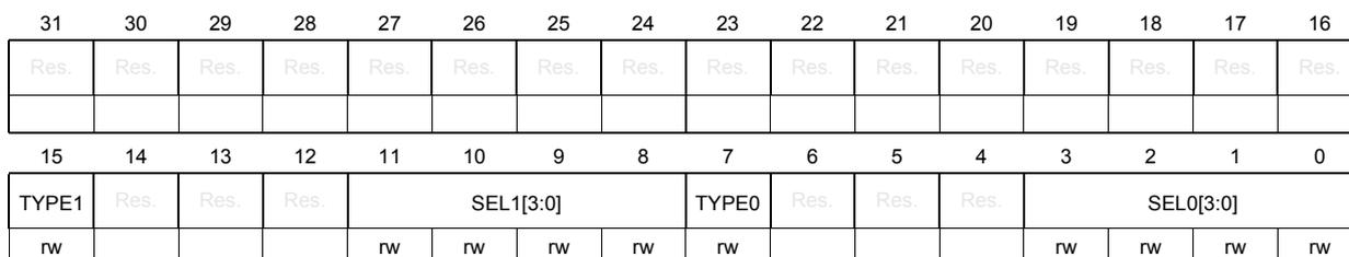
| 31 | 30 | 29 | 28 | 27 | 26 | 25 | 24 | 23 | 22 | 21 | 20 | 19 | 18 | 17 | 16 |
| Res. | Res. | Res. | Res. | Res. | Res. | Res. | Res. | Res. | Res. | Res. | Res. | Res. | Res. | Res. | Res. |
| 15 | 14 | 13 | 12 | 11 | 10 | 9 | 8 | 7 | 6 | 5 | 4 | 3 | 2 | 1 | 0 |
| TYPE1 | Res. | Res. | Res. | SEL1[3:0] | TYPE0 | Res. | Res. | Res. | SEL0[3:0] | ||||||
| rw | rw | rw | rw | rw | rw | rw | rw | rw | rw | ||||||
Bits 31:16 Reserved, must be kept at reset value.
Bit 15 TYPE1 : Resource type for event 1
0: Single selected resource
1: Boolean combined resource pair
Bits 14:12 Reserved, must be kept at reset value.
Bits 11:8 SEL1[3:0] : Resource / Boolean combined resource pair, for event 1
When TYPE1 is 0, selects a single selected resource from 0-15 defined by bits[3:0]
When TYPE1 is 1, selects a Boolean combined resource pair from 0-7 defined by bits[2:0]
Bit 7 TYPE0 : Resource type for event 0
0: Single selected resource
1: Boolean combined resource pair
Bits 6:4 Reserved, must be kept at reset value.
Bits 3:0 SEL0[3:0] : Resource / Boolean combined resource pair for event 0
When TYPE0 is 0, selects a single selected resource from 0-15 defined by bits[3:0]
When TYPE0 is 1, selects a Boolean combined resource pair from 0-7 defined by bits[2:0]
ETM event control 1 register (M7_ETM_EVENTCTL1)
Only accepts writes when trace unit is disabled
Address offset: 0x024
Reset value: 0x0000 0000
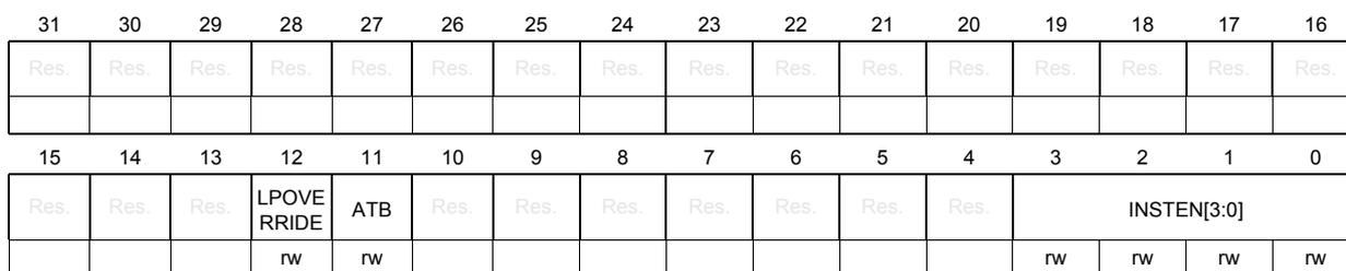
| 31 | 30 | 29 | 28 | 27 | 26 | 25 | 24 | 23 | 22 | 21 | 20 | 19 | 18 | 17 | 16 |
| Res. | Res. | Res. | Res. | Res. | Res. | Res. | Res. | Res. | Res. | Res. | Res. | Res. | Res. | Res. | Res. |
| 15 | 14 | 13 | 12 | 11 | 10 | 9 | 8 | 7 | 6 | 5 | 4 | 3 | 2 | 1 | 0 |
| Res. | Res. | Res. | LPOVER RIDE | ATB | Res. | Res. | Res. | Res. | Res. | Res. | Res. | INSTEN[3:0] | |||
| rw | rw | rw | rw | rw | rw | ||||||||||
Bits 31:13 Reserved, must be kept at reset value.
Bit 12 LPOVERRIDE : Low power state behavior override
0: Low power state normal behavior
1: Entry to low power state does not affect resources and event trace generation
Bit 11 ATB : ATB trigger enable
0: Disabled
1: Enabled
Bits 10:4 Reserved, must be kept at reset value.
Bits 3:0 INSTEN[3:0] : Instruction trace event element enable
Each bit corresponds to an event:
0bXXX0: Event 0 does not cause an event element
0bXXX1: Event 0 causes an event element
0bXX0X: Event 1 does not cause an event element
0bXX1X: Event 1 causes an event element
0bX0XX: Event 2 does not cause an event element
0bX1XX: Event 2 causes an event element
0b0XXX: Event 3 does not cause an event element
0b1XXX: Event 3 causes an event element
ETM stall control register (M7_ETM_STALLCTL)
Only accepts writes when trace unit is disabled
Address offset: 0x02C
Reset value: 0x0000 0000
| 31 | 30 | 29 | 28 | 27 | 26 | 25 | 24 | 23 | 22 | 21 | 20 | 19 | 18 | 17 | 16 |
|---|---|---|---|---|---|---|---|---|---|---|---|---|---|---|---|
| Res. | Res. | Res. | Res. | Res. | Res. | Res. | Res. | Res. | Res. | Res. | Res. | Res. | Res. | Res. | Res. |
| 15 | 14 | 13 | 12 | 11 | 10 | 9 | 8 | 7 | 6 | 5 | 4 | 3 | 2 | 1 | 0 |
| Res. | Res. | Res. | Res. | Res. | Res. | DSTALL L | ISTALL | Res. | Res. | Res. | Res. | LEVEL[1:0] | Res. | Res. | |
| rw | rw | rw | rw | ||||||||||||
Bits 31:10 Reserved, must be kept at reset value.
Bit 9 DSTALL : Stall processor based on data trace buffer space
0: Do not stall processor
1: Stall processor
Bit 8 ISTALL : Stall processor based on instruction trace buffer space
0: Do not stall processor
1: Stall processor
Bits 7:4 Reserved, must be kept at reset value.
Bits 3:2 LEVEL[1:0] : Stalling threshold level
A low level minimizes the amount of processor stalling, with a higher risk of FIFO overflow. A high level minimizes the risk of FIFO overflow but increases the amount of processor stalling.
Bits 1:0 Reserved, must be kept at reset value.
ETM global timestamp control register (M7_ETM_TSCTL)
Only accepts writes when trace unit is disabled
Address offset: 0x030
Reset value: 0x0000 0000
| 31 | 30 | 29 | 28 | 27 | 26 | 25 | 24 | 23 | 22 | 21 | 20 | 19 | 18 | 17 | 16 |
|---|---|---|---|---|---|---|---|---|---|---|---|---|---|---|---|
| Res. | Res. | Res. | Res. | Res. | Res. | Res. | Res. | Res. | Res. | Res. | Res. | Res. | Res. | Res. | Res. |
| 15 | 14 | 13 | 12 | 11 | 10 | 9 | 8 | 7 | 6 | 5 | 4 | 3 | 2 | 1 | 0 |
| Res. | Res. | Res. | Res. | Res. | Res. | Res. | Res. | TYPE | Res. | Res. | Res. | SEL[3:0] | |||
| rw | rw | rw | rw | rw | |||||||||||
Bits 31:8 Reserved, must be kept at reset value.
Bit 7 TYPE : Resource type for time stamp insertion
0: Single selected resource
1: Boolean combined resource pair
Bits 6:4 Reserved, must be kept at reset value.
Bits 3:0 SEL[3:0] : Resource / Boolean combined resource pair
When TYPE is 0, selects a single selected resource from 0-15 defined by bits[3:0]
When TYPE is 1, selects a Boolean combined resource pair from 0-7 defined by bits[2:0]
ETM synchronization period register (M7_ETM_SYNCP)
Address offset: 0x034
Reset value: 0x0000 000A
| 31 | 30 | 29 | 28 | 27 | 26 | 25 | 24 | 23 | 22 | 21 | 20 | 19 | 18 | 17 | 16 |
|---|---|---|---|---|---|---|---|---|---|---|---|---|---|---|---|
| Res. | Res. | Res. | Res. | Res. | Res. | Res. | Res. | Res. | Res. | Res. | Res. | Res. | Res. | Res. | Res. |
| 15 | 14 | 13 | 12 | 11 | 10 | 9 | 8 | 7 | 6 | 5 | 4 | 3 | 2 | 1 | 0 |
| Res. | Res. | Res. | Res. | Res. | Res. | Res. | Res. | Res. | Res. | Res. | PERIOD[4:0] | ||||
| r | r | r | r | r | |||||||||||
Bits 31:5 Reserved, must be kept at reset value.
Bits 4:0 PERIOD[4:0] : Trace bytes between synchronization requests
Defines the number of bytes of trace information between trace synchronization requests.
0xA: 1024 bytes
ETM cycle count control register (M7_ETM_CCCTL)
Address offset: 0x038
Reset value: 0x0000 0000
| 31 | 30 | 29 | 28 | 27 | 26 | 25 | 24 | 23 | 22 | 21 | 20 | 19 | 18 | 17 | 16 |
|---|---|---|---|---|---|---|---|---|---|---|---|---|---|---|---|
| Res. | Res. | Res. | Res. | Res. | Res. | Res. | Res. | Res. | Res. | Res. | Res. | Res. | Res. | Res. | Res. |
| 15 | 14 | 13 | 12 | 11 | 10 | 9 | 8 | 7 | 6 | 5 | 4 | 3 | 2 | 1 | 0 |
| Res. | Res. | Res. | Res. | THRESHOLD[11:0] | |||||||||||
| rw | rw | rw | rw | rw | rw | rw | rw | rw | rw | rw | |||||
Bits 31:12 Reserved, must be kept at reset value.
Bits 11:0 THRESHOLD[11:0] : Threshold value for instruction trace cycle counting
The threshold represents the minimum interval between cycle count trace packets.
0x0: Reserved
Other: Threshold
ETM trace ID register (M7_ETM_TRACEID)
Address offset: 0x040
Reset value: 0x0000 0000
| 31 | 30 | 29 | 28 | 27 | 26 | 25 | 24 | 23 | 22 | 21 | 20 | 19 | 18 | 17 | 16 |
|---|---|---|---|---|---|---|---|---|---|---|---|---|---|---|---|
| Res. | Res. | Res. | Res. | Res. | Res. | Res. | Res. | Res. | Res. | Res. | Res. | Res. | Res. | Res. | Res. |
| 15 | 14 | 13 | 12 | 11 | 10 | 9 | 8 | 7 | 6 | 5 | 4 | 3 | 2 | 1 | 0 |
| Res. | Res. | Res. | Res. | Res. | Res. | Res. | Res. | Res. | TRACEID[6:0] | ||||||
| rw | rw | rw | rw | rw | rw | rw | |||||||||
Bits 31:7 Reserved, must be kept at reset value.
Bits 6:0 TRACEID[6:0] : Trace ID
0x00: Reserved
0x01 to 0x6F: Valid ID
0x70 to 0x7F: Reserved
ETM ViewInst main control register (M7_ETM_VICTL)
Address offset: 0x080
Reset value: 0x0000 0000
| 31 | 30 | 29 | 28 | 27 | 26 | 25 | 24 | 23 | 22 | 21 | 20 | 19 | 18 | 17 | 16 |
|---|---|---|---|---|---|---|---|---|---|---|---|---|---|---|---|
| Res. | Res. | Res. | Res. | Res. | Res. | Res. | Res. | Res. | Res. | Res. | Res. | EXLEV EL_S3 | Res. | Res. | EXLEV EL_S0 |
| rw | rw | ||||||||||||||
| 15 | 14 | 13 | 12 | 11 | 10 | 9 | 8 | 7 | 6 | 5 | 4 | 3 | 2 | 1 | 0 |
| Res. | Res. | Res. | Res. | TRCE RR | TRCR ESET | SSSTA TUS | Res. | TYPE | Res. | Res. | Res. | SEL[3:0] | |||
| rw | rw | rw | rw | rw | rw | rw | rw | ||||||||
Bits 31:20 Reserved, must be kept at reset value.
Bit 19 EXLEVEL_S3 : Trace disable, exception level 3
Disables tracing in the specified exception level in Secure state for exception level 3.
0: Enable ViewInst in this exception level
1: Disable ViewInst in this exception level
Bits 18:17 Reserved, must be kept at reset value.
Bit 16 EXLEVEL_S0 : Trace disable, exception level 0
Disables tracing in the specified exception level in Secure state for exception level 0.
0: Enable ViewInst in this exception level
1: Disable ViewInst in this exception level
Bits 15:12 Reserved, must be kept at reset value.
Bit 11 TRCERR : Tracing of system error exception
Selects whether a system error exception must always be traced.
0: System error exception is traced only if the instruction or exception immediately before the system error exception is traced
1: System error exception is always traced regardless of the value of ViewInst
Bit 10 TRCRESET : Tracing of reset exception
Selects whether a reset exception must always be traced.
0: Reset exception is traced only if the instruction or exception immediately before the reset exception is traced
1: Reset exception is always traced regardless of the value of ViewInst
Bit 9 SSSTATUS : Current status of the start/stop logic
0: Stop state
1: Started state
Bit 8 Reserved, must be kept at reset value.
Bit 7 TYPE : Resource type
0: Single selected resource
1: Boolean combined resource pair
Bits 6:4 Reserved, must be kept at reset value.
Bits 3:0 SEL[3:0] : Resource / Boolean combined resource pair
When TYPE is 0, selects a single selected resource from 0-15 defined by bits[3:0]
When TYPE is 1, selects a Boolean combined resource pair from 0-7 defined by bits[2:0]
ETM ViewInst start/stop control register (M7_ETM_VISSCTL)
Address offset: 0x088
Reset value: 0x0000 0000
| 31 | 30 | 29 | 28 | 27 | 26 | 25 | 24 | 23 | 22 | 21 | 20 | 19 | 18 | 17 | 16 |
|---|---|---|---|---|---|---|---|---|---|---|---|---|---|---|---|
| Res. | Res. | Res. | Res. | Res. | Res. | Res. | Res. | STOP[7:0] | |||||||
| rw | rw | rw | rw | rw | rw | rw | rw | ||||||||
| 15 | 14 | 13 | 12 | 11 | 10 | 9 | 8 | 7 | 6 | 5 | 4 | 3 | 2 | 1 | 0 |
|---|---|---|---|---|---|---|---|---|---|---|---|---|---|---|---|
| Res. | Res. | Res. | Res. | Res. | Res. | Res. | Res. | START[7:0] | |||||||
| rw | rw | rw | rw | rw | rw | rw | rw | ||||||||
Bits 31:24 Reserved, must be kept at reset value.
Bits 23:16 STOP[7:0] : Selector of single address comparators to stop trace
Defines the single address comparators to stop trace with the ViewInst Start/Stop control.
One bit is provided for each implemented single address comparator.
Bits 15:8 Reserved, must be kept at reset value.
Bits 7:0 START[7:0] : Selector of single address comparators to start trace
Defines the single address comparators to start trace with the ViewInst Start/Stop control.
One bit is provided for each implemented single address comparator.
ETM ViewInst start/stop processor comparator control register (M7_ETM_VIPCSSCTL)
Address offset: 0x08C
Reset value: 0x0000 0000
| 31 | 30 | 29 | 28 | 27 | 26 | 25 | 24 | 23 | 22 | 21 | 20 | 19 | 18 | 17 | 16 |
|---|---|---|---|---|---|---|---|---|---|---|---|---|---|---|---|
| Res. | Res. | Res. | Res. | Res. | Res. | Res. | Res. | Res. | Res. | Res. | Res. | STOP[3:0] | |||
| rw | rw | rw | rw | ||||||||||||
| 15 | 14 | 13 | 12 | 11 | 10 | 9 | 8 | 7 | 6 | 5 | 4 | 3 | 2 | 1 | 0 |
|---|---|---|---|---|---|---|---|---|---|---|---|---|---|---|---|
| Res. | Res. | Res. | Res. | Res. | Res. | Res. | Res. | Res. | Res. | Res. | Res. | START[3:0] | |||
| rw | rw | rw | rw | ||||||||||||
Bits 31:20 Reserved, must be kept at reset value.
Bits 19:16 STOP[3:0] : Selector of processor comparator input to stop trace
Selects which processor comparator inputs are in use with ViewInst start-stop control, for the purpose of stopping trace. One bit is provided for each processor comparator input.
Bits 15:4 Reserved, must be kept at reset value.
Bits 3:0 START[3:0] : Selector of processor comparator input to start trace
Selects which processor comparator inputs are in use with ViewInst start-stop control, for the purpose of starting trace. One bit is provided for each processor comparator input.
ETM counter reload value register (M7_ETM_CNTRLDV)
Address offset: 0x140
Reset value: 0x0000 0000
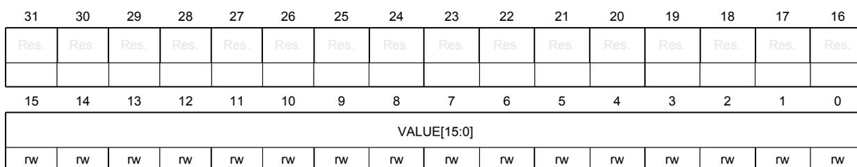
| 31 | 30 | 29 | 28 | 27 | 26 | 25 | 24 | 23 | 22 | 21 | 20 | 19 | 18 | 17 | 16 |
|---|---|---|---|---|---|---|---|---|---|---|---|---|---|---|---|
| Res. | Res. | Res. | Res. | Res. | Res. | Res. | Res. | Res. | Res. | Res. | Res. | Res. | Res. | Res. | Res. |
| 15 | 14 | 13 | 12 | 11 | 10 | 9 | 8 | 7 | 6 | 5 | 4 | 3 | 2 | 1 | 0 |
| VALUE[15:0] | |||||||||||||||
| rw | rw | rw | rw | rw | rw | rw | rw | rw | rw | rw | rw | rw | rw | rw | rw |
Bits 31:16 Reserved, must be kept at reset value.
Bits 15:0 VALUE[15:0] : Counter reload value
This value is loaded into the counter each time the reload event occurs.
ETM ID register 8 (M7_ETM_IDR8)
Address offset: 0x180
Reset value: 0x0000 0002
| 31 | 30 | 29 | 28 | 27 | 26 | 25 | 24 | 23 | 22 | 21 | 20 | 19 | 18 | 17 | 16 |
|---|---|---|---|---|---|---|---|---|---|---|---|---|---|---|---|
| MAXSPEC[31:16] | |||||||||||||||
| r | r | r | r | r | r | r | r | r | r | r | r | r | r | r | r |
| 15 | 14 | 13 | 12 | 11 | 10 | 9 | 8 | 7 | 6 | 5 | 4 | 3 | 2 | 1 | 0 |
| MAXSPEC[15:0] | |||||||||||||||
| r | r | r | r | r | r | r | r | r | r | r | r | r | r | r | r |
Bits 31:0 MAXSPEC[31:0] : Maximum speculation depth
Indicates the maximum speculation depth of the instruction trace stream. This is the maximum number of P0 elements that have not been committed in the trace stream at any one time.
0x2: Maximum trace speculation depth is 2
ETM ID register 9 (M7_ETM_IDR9)
Address offset: 0x184
Reset value: 0x0000 0000
| 31 | 30 | 29 | 28 | 27 | 26 | 25 | 24 | 23 | 22 | 21 | 20 | 19 | 18 | 17 | 16 |
|---|---|---|---|---|---|---|---|---|---|---|---|---|---|---|---|
| NUMP0KEY[31:16] | |||||||||||||||
| r | r | r | r | r | r | r | r | r | r | r | r | r | r | r | r |
| 15 | 14 | 13 | 12 | 11 | 10 | 9 | 8 | 7 | 6 | 5 | 4 | 3 | 2 | 1 | 0 |
| NUMP0KEY[15:0] | |||||||||||||||
| r | r | r | r | r | r | r | r | r | r | r | r | r | r | r | r |
Bits 31:0
NUMP0KEY[31:0]
: Number of P0 right-hand keys used
0x0: No P0 keys used in instruction trace only configuration
ETM ID register 10 (M7_ETM_IDR10)
Address offset: 0x188
Reset value: 0x0000 0000
| 31 | 30 | 29 | 28 | 27 | 26 | 25 | 24 | 23 | 22 | 21 | 20 | 19 | 18 | 17 | 16 |
|---|---|---|---|---|---|---|---|---|---|---|---|---|---|---|---|
| NUMP1KEY[31:16] | |||||||||||||||
| r | r | r | r | r | r | r | r | r | r | r | r | r | r | r | r |
| 15 | 14 | 13 | 12 | 11 | 10 | 9 | 8 | 7 | 6 | 5 | 4 | 3 | 2 | 1 | 0 |
| NUMP1KEY[15:0] | |||||||||||||||
| r | r | r | r | r | r | r | r | r | r | r | r | r | r | r | r |
Bits 31:0
NUMP1KEY[31:0]
: Total number of P1 right-hand keys
Indicates the total number of P1 right-hand keys, including normal and special keys.
0x0: No P1 keys used in instruction trace only configuration
ETM ID register 11 (M7_ETM_IDR11)
Address offset: 0x18C
Reset value: 0x0000 0000
| 31 | 30 | 29 | 28 | 27 | 26 | 25 | 24 | 23 | 22 | 21 | 20 | 19 | 18 | 17 | 16 |
|---|---|---|---|---|---|---|---|---|---|---|---|---|---|---|---|
| NUMP1SPC[31:16] | |||||||||||||||
| r | r | r | r | r | r | r | r | r | r | r | r | r | r | r | r |
| 15 | 14 | 13 | 12 | 11 | 10 | 9 | 8 | 7 | 6 | 5 | 4 | 3 | 2 | 1 | 0 |
| NUMP1SPC[15:0] | |||||||||||||||
| r | r | r | r | r | r | r | r | r | r | r | r | r | r | r | r |
Bits 31:0
NUMP1SPC[31:0]
: Total number of special P1 right-hand keys used
0x0: No special P1 keys used
Address offset: 0x190
Reset value: 0x0000 0001
| 31 | 30 | 29 | 28 | 27 | 26 | 25 | 24 | 23 | 22 | 21 | 20 | 19 | 18 | 17 | 16 |
| NUMCONDKEY[31:16] | |||||||||||||||
| r | r | r | r | r | r | r | r | r | r | r | r | r | r | r | r |
| 15 | 14 | 13 | 12 | 11 | 10 | 9 | 8 | 7 | 6 | 5 | 4 | 3 | 2 | 1 | 0 |
| NUMCONDKEY[15:0] | |||||||||||||||
| r | r | r | r | r | r | r | r | r | r | r | r | r | r | r | r |
Indicates the total number of conditional instruction right-hand keys, including normal and special keys.
0x1: One conditional instruction right hand-key implemented
ETM ID register 13 (M7_ETM_IDR13)Address offset: 0x194
Reset value: 0x0000 0001
| 31 | 30 | 29 | 28 | 27 | 26 | 25 | 24 | 23 | 22 | 21 | 20 | 19 | 18 | 17 | 16 |
| NUMCONDSPC[31:16] | |||||||||||||||
| r | r | r | r | r | r | r | r | r | r | r | r | r | r | r | r |
| 15 | 14 | 13 | 12 | 11 | 10 | 9 | 8 | 7 | 6 | 5 | 4 | 3 | 2 | 1 | 0 |
| NUMCONDSPC[15:0] | |||||||||||||||
| r | r | r | r | r | r | r | r | r | r | r | r | r | r | r | r |
0x0: No special conditional instruction right hand-keys implemented
ETM implementation specific register 0 (M7_ETM_IMSPEC0)Address offset: 0x1C0
Reset value: 0x0000 0000
| 31 | 30 | 29 | 28 | 27 | 26 | 25 | 24 | 23 | 22 | 21 | 20 | 19 | 18 | 17 | 16 |
| Res. | Res. | Res. | Res. | Res. | Res. | Res. | Res. | Res. | Res. | Res. | Res. | Res. | Res. | Res. | Res. |
| 15 | 14 | 13 | 12 | 11 | 10 | 9 | 8 | 7 | 6 | 5 | 4 | 3 | 2 | 1 | 0 |
| Res. | Res. | Res. | Res. | Res. | Res. | Res. | Res. | Res. | Res. | Res. | Res. | SUPPORT[3:0] | |||
| r | r | r | r | ||||||||||||
Bits 31:4 Reserved, must be kept at reset value.
Bits 3:0
SUPPORT[3:0]
: Support for implementation specific extensions
0x0: No implementation specific extensions are supported
ETM ID register 0 (M7_ETM_IDR0)
Address offset: 0x1E0
Reset value: 0x0C00 1EE1
| 31 | 30 | 29 | 28 | 27 | 26 | 25 | 24 | 23 | 22 | 21 | 20 | 19 | 18 | 17 | 16 |
|---|---|---|---|---|---|---|---|---|---|---|---|---|---|---|---|
| Res. | Res. | COMMOPT | TSSIZE[4:0] | Res. | Res. | Res. | Res. | Res. | Res. | Res. | QSUPP [1] | ||||
| r | r | r | r | r | r | r | |||||||||
| 15 | 14 | 13 | 12 | 11 | 10 | 9 | 8 | 7 | 6 | 5 | 4 | 3 | 2 | 1 | 0 |
|---|---|---|---|---|---|---|---|---|---|---|---|---|---|---|---|
| QSUPP [0] | Res. | CONDTYPE[1:0] | NUMEVENT[1:0] | RETSTACK | Res. | TRCCCI | TRCCOND | TRCBB | Res. | Res. | Res. | Res. | Res. | ||
| r | r | r | r | r | r | r | r | r | |||||||
Bits 31:30 Reserved, must be kept at reset value.
Bit 29
COMMOPT
: Meaning of the commit field in some packets
0: Commit mode 0
Bits 28:24
TSSIZE[4:0]
: Global timestamp size
0x08: Maximum of 64-bit global timestamp implemented
Bits 23:17 Reserved, must be kept at reset value.
Bits 16:15
QSUPP[1:0]
: Q element support
0x0: Q elements not supported
Bit 14 Reserved, must be kept at reset value.
Bits 13:12
CONDTYPE[1:0]
: Conditional result tracing type
0x1: APSR condition flag values traced
Bits 11:10
NUMEVENT[1:0]
: Number of events supported in the trace
0x1: Two events supported for instruction only configuration
Bit 9
RETSTACK
: Return stack support
1: Two entry return stack supported
Bit 8 Reserved, must be kept at reset value.
Bit 7
TRCCCI
: Support for cycle counting in the instruction trace
1: Cycle counting in the instruction trace is implemented
Bit 6
TRCCOND
: Support for conditional instruction tracing
1: Conditional instruction trace is implemented
Bit 5
TRCBB
: Support for branch broadcast tracing
1: Branch broadcast trace is implemented
Bits 4:0 Reserved, must be kept at reset value.
ETM ID register 1 (M7_ETM_IDR1)Address offset: 0x1E4
Reset value: 0x4100 F401
| 31 | 30 | 29 | 28 | 27 | 26 | 25 | 24 | 23 | 22 | 21 | 20 | 19 | 18 | 17 | 16 |
|---|---|---|---|---|---|---|---|---|---|---|---|---|---|---|---|
| DESIGNER[7:0] | Res. | Res. | Res. | Res. | Res. | Res. | Res. | Res. | |||||||
| r | r | r | r | r | r | r | r | ||||||||
| 15 | 14 | 13 | 12 | 11 | 10 | 9 | 8 | 7 | 6 | 5 | 4 | 3 | 2 | 1 | 0 |
| Res. | Res. | Res. | Res. | TRCARCHMAJ[3:0] | TRCARCHMIN[3:0] | REVISION[3:0] | |||||||||
| r | r | r | r | r | r | r | r | r | r | r | r | ||||
Bits 31:24
DESIGNER[7:0]
: Trace unit designer entity
0x41: Arm
®
Bits 23:12 Reserved, must be kept at reset value.
Bits 11:8
TRCARCHMAJ[3:0]
: Major trace unit architecture version number
0x4: ETM v4
Bits 7:4
TRCARCHMIN[3:0]
: Minor trace unit architecture version number
0x0: Minor version 0
Bits 3:0
REVISION[3:0]
: Implementation revision number
0x1: Rev 1
Address offset: 0x1E8
Reset value: 0x0000 0004
| 31 | 30 | 29 | 28 | 27 | 26 | 25 | 24 | 23 | 22 | 21 | 20 | 19 | 18 | 17 | 16 |
|---|---|---|---|---|---|---|---|---|---|---|---|---|---|---|---|
| Res. | Res. | Res. | CCSIZE[3:0] | DVSIZE[4:0] | DASIZE[4:1] | ||||||||||
| r | r | r | r | r | r | r | r | r | r | r | r | r | |||
| 15 | 14 | 13 | 12 | 11 | 10 | 9 | 8 | 7 | 6 | 5 | 4 | 3 | 2 | 1 | 0 |
| DASIZE[0] | VMIDSIZE[4:0] | CIDSIZE[4:0] | IASIZE[4:0] | ||||||||||||
| r | r | r | r | r | r | r | r | r | r | r | r | r | r | r | r |
Bits 31:29 Reserved, must be kept at reset value.
Bits 28:25
CCSIZE[3:0]
: Cycle counter size
Indicates the size of the cycle counter in bits minus 12.
0x0: Cycle counter is 12 bits
Bits 24:20
DVSIZE[4:0]
: Data value size in bytes
0x0: Data value size is not supported in instruction only configuration
Bits 19:15
DASIZE[4:0]
: Data address size in bytes
0x0: Data address size is not supported in instruction only configuration
- Bits 14:10
VMIDSIZE[4:0]
: Virtual machine ID size
0x0: Virtual machine ID tracing not implemented - Bits 9:5
CIDSIZE[4:0]
: Context ID size
0x0: Context ID tracing not implemented - Bits 4:0
IASIZE[4:0]
: Instruction address size
0x4: 32-bit maximum address size
ETM ID register 3 (M7_ETM_IDR3)
Address offset: 0x1EC
Reset value: 0x0509 0004
| 31 | 30 | 29 | 28 | 27 | 26 | 25 | 24 | 23 | 22 | 21 | 20 | 19 | 18 | 17 | 16 |
|---|---|---|---|---|---|---|---|---|---|---|---|---|---|---|---|
| NOOVERFLOW | NUMPROC[2:0] | SYSSTALL | STALLCTL | SYNCP R | TRCERR | Res. | Res. | Res. | Res. | EXLEVEL_S[3:0] | |||||
| r | r | r | r | r | r | r | r | r | r | r | r | ||||
| 15 | 14 | 13 | 12 | 11 | 10 | 9 | 8 | 7 | 6 | 5 | 4 | 3 | 2 | 1 | 0 |
| Res. | Res. | Res. | Res. | CCITMIN[11:0] | |||||||||||
| r | r | r | r | r | r | r | r | r | r | r | r | ||||
- Bit 31
NOOVERFLOW
: Support of NOOVERFLOW
Indicates whether the NOOVERFLOW of trace stall control is implemented.
0: Not implemented - Bits 30:28
NUMPROC[2:0]
: Number of processors available for tracing
0x0: Only one processor can be traced - Bit 27
SYSSTALL
: System support for stall control of the processor
0: Not supported - Bit 26
STALLCTL
: Stall control support
1: Trace stall control (TRCSTALLCTL) is implemented - Bit 25
SYNCP R
: Trace synchronization period support
0: TRCSYNCP R is read-only for instruction trace only configuration; the trace synchronization period is fixed - Bit 24
TRCERR
: Support of TRCVICTLR.TRCERR
Indicates whether TRCVICTLR.TRCERR is implemented.
0x4: 32-bit maximum address size - Bits 23:20 Reserved, must be kept at reset value.
- Bits 19:16
EXLEVEL_S[3:0]
: Support of privilege levels
Privilege levels are implemented; one bit for each level.
0x9: Privilege levels Thread and Handler are implemented - Bits 15:12 Reserved, must be kept at reset value.
- Bits 11:0
CCITMIN[11:0]
: Instruction trace cycle counting minimum threshold
0x4: Minimum threshold is 4 instruction trace cycle
ETM ID register 4 (M7_ETM_IDR4)
Address offset: 0x1F0
Reset value: 0x0001 4000
| 31 | 30 | 29 | 28 | 27 | 26 | 25 | 24 | 23 | 22 | 21 | 20 | 19 | 18 | 17 | 16 |
|---|---|---|---|---|---|---|---|---|---|---|---|---|---|---|---|
| NUMVMIDC[3:0] | NUMCIDC[3:0] | NUMSSCC[3:0] | NUMRSPAIR[3:0] | ||||||||||||
| r | r | r | r | r | r | r | r | r | r | r | r | r | r | r | r |
| 15 | 14 | 13 | 12 | 11 | 10 | 9 | 8 | 7 | 6 | 5 | 4 | 3 | 2 | 1 | 0 |
| NUMPC[3:0] | Res. | Res. | Res. | SUPPA DC | NUMDVC[3:0] | NUMACPAIRS[3:0] | |||||||||
| r | r | r | r | r | r | r | r | r | r | r | r | r | |||
Bits 31:28 NUMVMIDC[3:0] : Number of Virtual Machine ID comparators implemented
0x0: None
Bits 27:24 NUMCIDC[3:0] : Number of Context ID comparators implemented
0x0: None
Bits 23:20 NUMSSCC[3:0] : Number of single-shot comparator controls implemented
0x0: None
Bits 19:16 NUMRSPAIR[3:0] : Number of resource selection pairs implemented
0x1: None
Bits 15:12 NUMPC[3:0] : Number of processor comparator inputs implemented
0x4: Four
Bits 11:9 Reserved, must be kept at reset value.
Bit 8 SUPPADDC : Support of data address comparisons
0: Not implemented
Bits 7:4 NUMDVC[3:0] : Number of data value comparators implemented
0x0: None
Bits 3:0 NUMACPAIRS[3:0] : Number of address comparator pairs implemented.
0x0: None
ETM ID register 5 (M7_ETM_IDR5)
Address offset: 0x1F4
Reset value: 0x90C7 0402
| 31 | 30 | 29 | 28 | 27 | 26 | 25 | 24 | 23 | 22 | 21 | 20 | 19 | 18 | 17 | 16 |
|---|---|---|---|---|---|---|---|---|---|---|---|---|---|---|---|
| REDF UNCN TR | NUMCNTR[2:0] | NUMSEQSTATE[2:0] | Res. | LPOVE RRIDE | ATBTRI G | TRACEIDSIZE[5:0] | |||||||||
| r | r | r | r | r | r | r | r | r | r | r | r | r | r | r | |
| 15 | 14 | 13 | 12 | 11 | 10 | 9 | 8 | 7 | 6 | 5 | 4 | 3 | 2 | 1 | 0 |
| Res. | Res. | Res. | Res. | NUMEXTINSEL[2:0] | NUMEXTIN[8:0] | ||||||||||
| r | r | r | r | r | r | r | r | r | r | r | r | ||||
- Bit 31
REDFUNCNTR
: Support of reduced function counter
1: Implemented - Bits 30:28
NUMCNTR[2:0]
: Number of counters implemented
0x1: One counter implemented - Bits 27:25
NUMSEQSTATE[2:0]
: Number of sequencer states implemented
0x0: None - Bit 24 Reserved, must be kept at reset value.
- Bit 23
LPOVERRIDE
: Support of low-power state override
1: Implemented - Bit 22
ATBTRIG
: Support of ATB trigger
1: Implemented - Bits 21:16
TRACEIDSIZE[5:0]
: Number of trace ID bits
0x07: Seven-bit trace ID implemented. - Bits 15:12 Reserved, must be kept at reset value.
- Bits 11:9
NUMEXTINSEL[2:0]
: Number of implemented external input selectors
0x2: Two external input selectors implemented - Bits 8:0
NUMEXTIN[8:0]
: Number of implemented external inputs
0x2: Two external inputs implemented
ETM resource selection register 2 (M7_ETM_RSCTL2)
Address offset: 0x208
Reset value: 0x0000 0000
| 31 | 30 | 29 | 28 | 27 | 26 | 25 | 24 | 23 | 22 | 21 | 20 | 19 | 18 | 17 | 16 |
|---|---|---|---|---|---|---|---|---|---|---|---|---|---|---|---|
| Res. | Res. | Res. | Res. | Res. | Res. | Res. | Res. | Res. | Res. | PAIRINV | INV | Res. | GROUP[2:0] | ||
| rw | rw | rw | rw | rw | |||||||||||
| 15 | 14 | 13 | 12 | 11 | 10 | 9 | 8 | 7 | 6 | 5 | 4 | 3 | 2 | 1 | 0 |
| Res. | Res. | Res. | Res. | Res. | Res. | Res. | Res. | SELECT[7:0] | |||||||
| rw | rw | rw | rw | rw | rw | rw | rw | ||||||||
- Bits 31:22 Reserved, must be kept at reset value.
- Bit 21
PAIRINV
: Inversion of result of a combined pair of resources
0: Not inverted
1: Inverted - Bit 20
INV
: Inversion of the selected resources
0: Not inverted
1: Inverted - Bit 19 Reserved, must be kept at reset value.
Bits 18:16 GROUP[2:0] : Selects a group of resources
Bits 15:8 Reserved, must be kept at reset value.
Bits 7:0 SELECT[7:0] : Selector of resources from desired group
Selects one or more resources from the desired group. One bit is provided per resource from the group.
ETM resource selection register 3 (M7_ETM_RSCTL3)
Address offset: 0x20C
Reset value: 0x0000 0000
| 31 | 30 | 29 | 28 | 27 | 26 | 25 | 24 | 23 | 22 | 21 | 20 | 19 | 18 | 17 | 16 |
|---|---|---|---|---|---|---|---|---|---|---|---|---|---|---|---|
| Res. | Res. | Res. | Res. | Res. | Res. | Res. | Res. | Res. | Res. | Res. | INV | Res. | GROUP[2:0] | ||
| rw | rw | rw | rw | ||||||||||||
| 15 | 14 | 13 | 12 | 11 | 10 | 9 | 8 | 7 | 6 | 5 | 4 | 3 | 2 | 1 | 0 |
|---|---|---|---|---|---|---|---|---|---|---|---|---|---|---|---|
| Res. | Res. | Res. | Res. | Res. | Res. | Res. | Res. | SELECT[7:0] | |||||||
| rw | rw | rw | rw | rw | rw | rw | rw | ||||||||
Bits 31:21 Reserved, must be kept at reset value.
Bit 20 INV : Inversion of the selected resources
0: Not inverted
1: Inverted
Bit 19 Reserved, must be kept at reset value.
Bits 18:16 GROUP[2:0] : Selects a group of resources
Bits 15:8 Reserved, must be kept at reset value.
Bits 7:0 SELECT[7:0] : Selector of resources from desired group
Selects one or more resources from the desired group. One bit is provided per resource from the group.
ETM single-shot comparator control register 0 (M7_ETM_SSCC0)
Address offset: 0x280
Reset value: 0x0000 0000
| 31 | 30 | 29 | 28 | 27 | 26 | 25 | 24 | 23 | 22 | 21 | 20 | 19 | 18 | 17 | 16 |
|---|---|---|---|---|---|---|---|---|---|---|---|---|---|---|---|
| Res. | Res. | Res. | Res. | Res. | Res. | Res. | RST | Res. | Res. | Res. | Res. | Res. | Res. | Res. | Res. |
| rw |
| 15 | 14 | 13 | 12 | 11 | 10 | 9 | 8 | 7 | 6 | 5 | 4 | 3 | 2 | 1 | 0 |
|---|---|---|---|---|---|---|---|---|---|---|---|---|---|---|---|
| Res. | Res. | Res. | Res. | Res. | Res. | Res. | Res. | Res. | Res. | Res. | Res. | Res. | Res. | Res. | Res. |
Bits 31:25 Reserved, must be kept at reset value.
Bit 24 RST : Single-shot comparator resource reset enable
Enables the single-shot comparator resource to be reset when it occurs, then enables another comparator match to be detected.
0: Disabled
1: Reset enabled; multiple matches can occur
Bits 23:0 Reserved, must be kept at reset value.
ETM single-shot comparator status register 0 (M7_ETM_SSCS0)
Address offset: 0x2A0
Reset value: 0x0000 0001
| 31 | 30 | 29 | 28 | 27 | 26 | 25 | 24 | 23 | 22 | 21 | 20 | 19 | 18 | 17 | 16 |
|---|---|---|---|---|---|---|---|---|---|---|---|---|---|---|---|
| STATUS | Res. | Res. | Res. | Res. | Res. | Res. | Res. | Res. | Res. | Res. | Res. | Res. | Res. | Res. | Res. |
| rw | |||||||||||||||
| 15 | 14 | 13 | 12 | 11 | 10 | 9 | 8 | 7 | 6 | 5 | 4 | 3 | 2 | 1 | 0 |
| Res. | Res. | Res. | Res. | Res. | Res. | Res. | Res. | Res. | Res. | Res. | Res. | Res. | DV | DA | INST |
| r | r | r |
Bit 31 STATUS : Single-shot status
This indicates whether any of the selected comparators have matched. If SSCS0.RST is set to 0, the STATUS bit must be written with 0 in order to enable single-shot comparator control.
0: No match occurred
1: Match has occurred at least once.
Bits 30:3 Reserved, must be kept at reset value.
Bit 2 DV : Data value comparator support
0: Single-shot data value comparisons not supported
Bit 1 DA : Data address comparator support
0: Single-shot data address comparisons not supported
Bit 0 INST : Instruction address comparator support
1: Single-shot instruction address comparisons supported
ETM single-shot processor comparator input control register (M7_ETM_SSPCIC0)
Address offset: 0x2C0
Reset value: 0x0000 0000
| 31 | 30 | 29 | 28 | 27 | 26 | 25 | 24 | 23 | 22 | 21 | 20 | 19 | 18 | 17 | 16 |
|---|---|---|---|---|---|---|---|---|---|---|---|---|---|---|---|
| Res. | Res. | Res. | Res. | Res. | Res. | Res. | Res. | Res. | Res. | Res. | Res. | Res. | Res. | Res. | Res. |
| 15 | 14 | 13 | 12 | 11 | 10 | 9 | 8 | 7 | 6 | 5 | 4 | 3 | 2 | 1 | 0 |
| Res. | Res. | Res. | Res. | Res. | Res. | Res. | Res. | ||||||||
| rw | rw | rw | rw | rw | rw | rw | rw |
Bits 31:8 Reserved, must be kept at reset value.
Bits 7:0 PC[7:0] : Comparator input selector for single-shot control
Selects one or more processor comparator inputs for single-shot control. One bit is provided for each processor comparator input.
ETM power-down control register (M7_ETM_PDC)
Address offset: 0x310
Reset value: 0x0000 0000
| 31 | 30 | 29 | 28 | 27 | 26 | 25 | 24 | 23 | 22 | 21 | 20 | 19 | 18 | 17 | 16 |
|---|---|---|---|---|---|---|---|---|---|---|---|---|---|---|---|
| Res. | Res. | Res. | Res. | Res. | Res. | Res. | Res. | Res. | Res. | Res. | Res. | Res. | Res. | Res. | Res. |
| 15 | 14 | 13 | 12 | 11 | 10 | 9 | 8 | 7 | 6 | 5 | 4 | 3 | 2 | 1 | 0 |
| Res. | Res. | Res. | Res. | Res. | Res. | Res. | Res. | Res. | Res. | Res. | Res. | PU | Res. | Res. | Res. |
| r |
Bits 31:4 Reserved, must be kept at reset value.
Bit 3 PU : Power up request
Request to maintain power to the ETM and access to the trace registers.
0: Power not requested
1: Power requested
Bits 2:0 Reserved, must be kept at reset value.
ETM power-down status register (M7_ETM_PDS)
Address offset: 0x314
Reset value: 0x0000 0003
| 31 | 30 | 29 | 28 | 27 | 26 | 25 | 24 | 23 | 22 | 21 | 20 | 19 | 18 | 17 | 16 |
|---|---|---|---|---|---|---|---|---|---|---|---|---|---|---|---|
| Res. | Res. | Res. | Res. | Res. | Res. | Res. | Res. | Res. | Res. | Res. | Res. | Res. | Res. | Res. | Res. |
| 15 | 14 | 13 | 12 | 11 | 10 | 9 | 8 | 7 | 6 | 5 | 4 | 3 | 2 | 1 | 0 |
| Res. | Res. | Res. | Res. | Res. | Res. | Res. | Res. | Res. | Res. | Res. | Res. | Res. | Res. | STICKY PD | POWE R |
| r | r |
Bits 31:2 Reserved, must be kept at reset value.
Bit 1 STICKYPD : Sticky power-down state
This bit is set to 1 when power to the ETM registers is removed, to indicate that programming state has been lost. It is cleared after a read of the TRCPDSR.
0: Trace register power uninterrupted since the last read of PDS register
1: Trace register power interrupted since the last read of PDS register
Bit 0 POWER : ETM powered up
1: ETM is powered up; all registers are accessible
ETM claim tag set register (M7_ETM_CLAIMSET)
Address offset: 0xFA0
Reset value: 0x0000 000F
| 31 | 30 | 29 | 28 | 27 | 26 | 25 | 24 | 23 | 22 | 21 | 20 | 19 | 18 | 17 | 16 |
|---|---|---|---|---|---|---|---|---|---|---|---|---|---|---|---|
| Res. | Res. | Res. | Res. | Res. | Res. | Res. | Res. | Res. | Res. | Res. | Res. | Res. | Res. | Res. | Res. |
| 15 | 14 | 13 | 12 | 11 | 10 | 9 | 8 | 7 | 6 | 5 | 4 | 3 | 2 | 1 | 0 |
| Res. | Res. | Res. | Res. | Res. | Res. | Res. | Res. | Res. | Res. | Res. | Res. | CLAIMSET[3:0] | |||
| rw | rw | rw | rw | ||||||||||||
Bits 31:4 Reserved, must be kept at reset value.
Bits 3:0 CLAIMSET[3:0] : Set claim tag bits
Write:
0000: No effect
xxx1: Set bit 0
xx1x: Set bit 1
x1xx: Set bit 2
1xxx: Set bit 3
Read:
0xF: Indicates there are four bits in claim tag
ETM claim tag clear register (M7_ETM_CLAIMCLR)
Address offset: 0xFA4
Reset value: 0x0000 0000
| 31 | 30 | 29 | 28 | 27 | 26 | 25 | 24 | 23 | 22 | 21 | 20 | 19 | 18 | 17 | 16 |
|---|---|---|---|---|---|---|---|---|---|---|---|---|---|---|---|
| Res. | Res. | Res. | Res. | Res. | Res. | Res. | Res. | Res. | Res. | Res. | Res. | Res. | Res. | Res. | Res. |
| 15 | 14 | 13 | 12 | 11 | 10 | 9 | 8 | 7 | 6 | 5 | 4 | 3 | 2 | 1 | 0 |
| Res. | Res. | Res. | Res. | Res. | Res. | Res. | Res. | Res. | Res. | Res. | Res. | CLAIMCLR[3:0] | |||
| rw | rw | rw | rw | ||||||||||||
Bits 31:4 Reserved, must be kept at reset value.
Bits 3:0 CLAIMCLR[3:0] : Reset claim tag bits
Write:
0000: No effect
xxx1: Clear bit 0
xx1x: Clear bit 1
x1xx: Clear bit 2
1xxx: Clear bit 3
Read: Returns current value of claim tag
ETM lock access register (M7_ETM_LAR)
Address offset: 0xFB0
Reset value: N/A
| 31 | 30 | 29 | 28 | 27 | 26 | 25 | 24 | 23 | 22 | 21 | 20 | 19 | 18 | 17 | 16 |
|---|---|---|---|---|---|---|---|---|---|---|---|---|---|---|---|
| ACCESS_W[31:16] | |||||||||||||||
| w | w | w | w | w | w | w | w | w | w | w | w | w | w | w | w |
| 15 | 14 | 13 | 12 | 11 | 10 | 9 | 8 | 7 | 6 | 5 | 4 | 3 | 2 | 1 | 0 |
| ACCESS_W[15:0] | |||||||||||||||
| w | w | w | w | w | w | w | w | w | w | w | w | w | w | w | w |
Bits 31:0 ACCESS_W[31:0] : ETM register write access
Enables write access to some ETM registers by processor cores (debuggers do not need to unlock the component)
0xC5ACCE55: Enable write access
Other values: Disable write access
ETM lock status register (M7_ETM_LSR)Address offset: 0xFB4
Reset value: 0x0000 0003
| 31 | 30 | 29 | 28 | 27 | 26 | 25 | 24 | 23 | 22 | 21 | 20 | 19 | 18 | 17 | 16 |
|---|---|---|---|---|---|---|---|---|---|---|---|---|---|---|---|
| Res. | Res. | Res. | Res. | Res. | Res. | Res. | Res. | Res. | Res. | Res. | Res. | Res. | Res. | Res. | Res. |
| 15 | 14 | 13 | 12 | 11 | 10 | 9 | 8 | 7 | 6 | 5 | 4 | 3 | 2 | 1 | 0 |
| Res. | Res. | Res. | Res. | Res. | Res. | Res. | Res. | Res. | Res. | Res. | Res. | Res. | LOCKTYPE | LOCKGRANT | LOCKEXIST |
| r | r | r |
Bits 31:3 Reserved, must be kept at reset value.
Bit 2 LOCKTYPE : Size of the M7_ETM_LAR register0: 32-bit
Bit 1 LOCKGRANT : Current status of lockThis bit always returns zero when read by an external debugger.
0: Write access is permitted
1: Write access is blocked. Only read access is permitted.
Bit 0 LOCKEXIST : Existence of lock control mechanismThe bit indicates whether a lock control mechanism exists. It always returns zero when read by an external debugger.
0: No lock control mechanism exists
1: Lock control mechanism is implemented
ETM authentication status register (M7_ETM_AUTHSTAT)Address offset: 0xFB8
Reset value: 0x0000 000A
| 31 | 30 | 29 | 28 | 27 | 26 | 25 | 24 | 23 | 22 | 21 | 20 | 19 | 18 | 17 | 16 |
|---|---|---|---|---|---|---|---|---|---|---|---|---|---|---|---|
| Res. | Res. | Res. | Res. | Res. | Res. | Res. | Res. | Res. | Res. | Res. | Res. | Res. | Res. | Res. | Res. |
| 15 | 14 | 13 | 12 | 11 | 10 | 9 | 8 | 7 | 6 | 5 | 4 | 3 | 2 | 1 | 0 |
| Res. | Res. | Res. | Res. | Res. | Res. | Res. | Res. | SNID[1:0] | SID[1:0] | NSNID[1:0] | NSID[1:0] | ||||
| r | r | r | r | r | r | r | r |
Bits 31:8 Reserved, must be kept at reset value.
Bits 7:6 SNID[1:0] : Security level for secure non-invasive debug0x0: Not implemented
Bits 5:4 SID[1:0] : Security level for secure invasive debug
0x0: Not implemented
Bits 3:2 NSNID[1:0] : Security level for non-secure non-invasive debug
0x2: Disabled
0x3: Enabled
Bits 1:0 NSID[1:0] : Security level for non-secure invasive debug
0x2: Disabled
0x3: Enabled
ETM CoreSight device architecture register (M7_ETM_DEVARCH)
Address offset: 0xFBC
Reset value: 0x4770 4A13
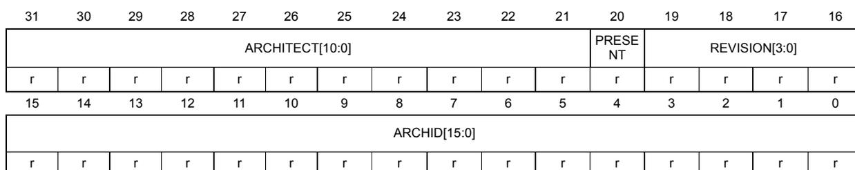
| 31 | 30 | 29 | 28 | 27 | 26 | 25 | 24 | 23 | 22 | 21 | 20 | 19 | 18 | 17 | 16 |
| ARCHITECT[10:0] | PRESENT | REVISION[3:0] | |||||||||||||
| r | r | r | r | r | r | r | r | r | r | r | r | r | r | r | r |
| 15 | 14 | 13 | 12 | 11 | 10 | 9 | 8 | 7 | 6 | 5 | 4 | 3 | 2 | 1 | 0 |
| ARCHID[15:0] | |||||||||||||||
| r | r | r | r | r | r | r | r | r | r | r | r | r | r | r | r |
Bits 31:21 ARCHITECT[10:0] : Component architect
0x23B: Arm ®
Bit 20 PRESENT : Indicates the presence of this register
1: Present
Bits 19:16 REVISION[3:0] : Architecture revision
0x0: Rev 0
Bits 15:0 ARCHID[15:0] : Architecture ID
0x4A13: ETMv4 component
ETM CoreSight device type identity register (M7_ETM_DEVTYPE)
Address offset: 0xFCC
Reset value: 0x0000 0013
| 31 | 30 | 29 | 28 | 27 | 26 | 25 | 24 | 23 | 22 | 21 | 20 | 19 | 18 | 17 | 16 |
| Res. | Res. | Res. | Res. | Res. | Res. | Res. | Res. | Res. | Res. | Res. | Res. | Res. | Res. | Res. | Res. |
| 15 | 14 | 13 | 12 | 11 | 10 | 9 | 8 | 7 | 6 | 5 | 4 | 3 | 2 | 1 | 0 |
| Res. | Res. | Res. | Res. | Res. | Res. | Res. | Res. | SUBTYPE[3:0] | MAJORTYPE[3:0] | ||||||
| r | r | r | r | r | r | r | r | ||||||||
Bits 31:8 Reserved, must be kept at reset value.
Bits 7:4
SUBTYPE[3:0]
: Device sub-type identifier
0x1: Processor trace
Bits 3:0
MAJORTYPE[3:0]
: Device main type identifier
0x3: Trace source
ETM CoreSight peripheral identity register 4 (M7_ETM_PIDR4)
Address offset: 0xFD0
Reset value: 0x0000 0004
| 31 | 30 | 29 | 28 | 27 | 26 | 25 | 24 | 23 | 22 | 21 | 20 | 19 | 18 | 17 | 16 |
|---|---|---|---|---|---|---|---|---|---|---|---|---|---|---|---|
| Res. | Res. | Res. | Res. | Res. | Res. | Res. | Res. | Res. | Res. | Res. | Res. | Res. | Res. | Res. | Res. |
| 15 | 14 | 13 | 12 | 11 | 10 | 9 | 8 | 7 | 6 | 5 | 4 | 3 | 2 | 1 | 0 |
| Res. | Res. | Res. | Res. | Res. | Res. | Res. | Res. | 4KCOUNT[3:0] | JEP106CON[3:0] | ||||||
| r | r | r | r | r | r | r | r | ||||||||
Bits 31:8 Reserved, must be kept at reset value.
Bits 7:4
4KCOUNT[3:0]
: Register file size
0x0: Register file occupies a single 4 Kbyte region
Bits 3:0
JEP106CON[3:0]
: JEP106 continuation code
0x4: Arm® JEDEC code
ETM CoreSight peripheral identity register 0 (M7_ETM_PIDR0)
Address offset: 0xFE0
Reset value: 0x0000 0075
| 31 | 30 | 29 | 28 | 27 | 26 | 25 | 24 | 23 | 22 | 21 | 20 | 19 | 18 | 17 | 16 |
|---|---|---|---|---|---|---|---|---|---|---|---|---|---|---|---|
| Res. | Res. | Res. | Res. | Res. | Res. | Res. | Res. | Res. | Res. | Res. | Res. | Res. | Res. | Res. | Res. |
| 15 | 14 | 13 | 12 | 11 | 10 | 9 | 8 | 7 | 6 | 5 | 4 | 3 | 2 | 1 | 0 |
| Res. | Res. | Res. | Res. | Res. | Res. | Res. | Res. | PARTNUM[7:0] | |||||||
| r | r | r | r | r | r | r | r | ||||||||
Bits 31:8 Reserved, must be kept at reset value.
Bits 7:0
PARTNUM[7:0]
: Part number field, field, bits [7:0]
0x75: ETM part number
ETM CoreSight peripheral identity register 1 (M7_ETM_PIDR1)
Address offset: 0xFE4
Reset value: 0x0000 00B9
| 31 | 30 | 29 | 28 | 27 | 26 | 25 | 24 | 23 | 22 | 21 | 20 | 19 | 18 | 17 | 16 |
|---|---|---|---|---|---|---|---|---|---|---|---|---|---|---|---|
| Res. | Res. | Res. | Res. | Res. | Res. | Res. | Res. | Res. | Res. | Res. | Res. | Res. | Res. | Res. | Res. |
| 15 | 14 | 13 | 12 | 11 | 10 | 9 | 8 | 7 | 6 | 5 | 4 | 3 | 2 | 1 | 0 |
| Res. | Res. | Res. | Res. | Res. | Res. | Res. | Res. | JEP106ID[3:0] | PARTNUM[11:8] | ||||||
| r | r | r | r | r | r | r | r | ||||||||
Bits 31:8 Reserved, must be kept at reset value.
Bits 7:4 JEP106ID[3:0] : JEP106 identity code field, bits [3:0]
0xB: Arm ® JEDEC code
Bits 3:0 PARTNUM[11:8] : Part number field, bits [11:8]
0x9: ETM part number
ETM CoreSight peripheral identity register 2 (M7_ETM_PIDR2)
Address offset: 0xFE8
Reset value: 0x0000 001B
| 31 | 30 | 29 | 28 | 27 | 26 | 25 | 24 | 23 | 22 | 21 | 20 | 19 | 18 | 17 | 16 |
|---|---|---|---|---|---|---|---|---|---|---|---|---|---|---|---|
| Res. | Res. | Res. | Res. | Res. | Res. | Res. | Res. | Res. | Res. | Res. | Res. | Res. | Res. | Res. | Res. |
| 15 | 14 | 13 | 12 | 11 | 10 | 9 | 8 | 7 | 6 | 5 | 4 | 3 | 2 | 1 | 0 |
| Res. | Res. | Res. | Res. | Res. | Res. | Res. | Res. | REVISION[3:0] | JEDEC | JEP106ID[6:4] | |||||
| r | r | r | r | r | r | r | r | ||||||||
Bits 31:8 Reserved, must be kept at reset value.
Bits 7:4 REVISION[3:0] : Component revision number
0x1: r0p2
Bit 3 JEDEC : JEDEC assigned value
1: Designer ID specified by JEDEC
Bits 2:0 JEP106ID[6:4] : JEP106 identity code field, bits [6:4]
0x3: Arm ® JEDEC code
ETM CoreSight peripheral identity register 3 (M7_ETM_PIDR3)Address offset: 0xFEC
Reset value: 0x0000 0000
| 31 | 30 | 29 | 28 | 27 | 26 | 25 | 24 | 23 | 22 | 21 | 20 | 19 | 18 | 17 | 16 |
|---|---|---|---|---|---|---|---|---|---|---|---|---|---|---|---|
| Res. | Res. | Res. | Res. | Res. | Res. | Res. | Res. | Res. | Res. | Res. | Res. | Res. | Res. | Res. | Res. |
| 15 | 14 | 13 | 12 | 11 | 10 | 9 | 8 | 7 | 6 | 5 | 4 | 3 | 2 | 1 | 0 |
| Res. | Res. | Res. | Res. | Res. | Res. | Res. | Res. | REVAND[3:0] | CMOD[3:0] | ||||||
| r | r | r | r | r | r | r | r | ||||||||
Bits 31:8 Reserved, must be kept at reset value.
Bits 7:4 REVAND[3:0] : Metal fix version0x0: No metal fix
Bits 3:0 CMOD[3:0] : Customer modified0x0: No customer modifications
ETM CoreSight component identity register 0 (M7_ETM_CIDR0)Address offset: 0xFF0
Reset value: 0x0000 000D
| 31 | 30 | 29 | 28 | 27 | 26 | 25 | 24 | 23 | 22 | 21 | 20 | 19 | 18 | 17 | 16 |
|---|---|---|---|---|---|---|---|---|---|---|---|---|---|---|---|
| Res. | Res. | Res. | Res. | Res. | Res. | Res. | Res. | Res. | Res. | Res. | Res. | Res. | Res. | Res. | Res. |
| 15 | 14 | 13 | 12 | 11 | 10 | 9 | 8 | 7 | 6 | 5 | 4 | 3 | 2 | 1 | 0 |
| Res. | Res. | Res. | Res. | Res. | Res. | Res. | Res. | PREAMBLE[7:0] | |||||||
| r | r | r | r | r | r | r | r | ||||||||
Bits 31:8 Reserved, must be kept at reset value.
Bits 7:0 PREAMBLE[7:0] : Component ID field, bits [7:0]0x0D: Common ID value
ETM CoreSight component identity register 1 (M7_ETM_CIDR1)Address offset: 0xFF4
Reset value: 0x0000 0090
| 31 | 30 | 29 | 28 | 27 | 26 | 25 | 24 | 23 | 22 | 21 | 20 | 19 | 18 | 17 | 16 |
|---|---|---|---|---|---|---|---|---|---|---|---|---|---|---|---|
| Res. | Res. | Res. | Res. | Res. | Res. | Res. | Res. | Res. | Res. | Res. | Res. | Res. | Res. | Res. | Res. |
| 15 | 14 | 13 | 12 | 11 | 10 | 9 | 8 | 7 | 6 | 5 | 4 | 3 | 2 | 1 | 0 |
|---|---|---|---|---|---|---|---|---|---|---|---|---|---|---|---|
| Res. | Res. | Res. | Res. | Res. | Res. | Res. | Res. | CLASS[3:0] | PREAMBLE[11:8] | ||||||
| r | r | r | r | r | r | r | r | ||||||||
Bits 31:8 Reserved, must be kept at reset value.
Bits 7:4 CLASS[3:0] : Component ID field, bits [15:12] - component class
0x9: Debug component with CoreSight-compatible registers
Bits 3:0 PREAMBLE[11:8] : Component ID field, bits [11:8]
0x0: Common ID value
ETM CoreSight component identity register 2 (M7_ETM_CIDR2)
Address offset: 0xFF8
Reset value: 0x0000 0005
| 31 | 30 | 29 | 28 | 27 | 26 | 25 | 24 | 23 | 22 | 21 | 20 | 19 | 18 | 17 | 16 |
|---|---|---|---|---|---|---|---|---|---|---|---|---|---|---|---|
| Res. | Res. | Res. | Res. | Res. | Res. | Res. | Res. | Res. | Res. | Res. | Res. | Res. | Res. | Res. | Res. |
| 15 | 14 | 13 | 12 | 11 | 10 | 9 | 8 | 7 | 6 | 5 | 4 | 3 | 2 | 1 | 0 |
| Res. | Res. | Res. | Res. | Res. | Res. | Res. | Res. | PREAMBLE[19:12] | |||||||
| r | r | r | r | r | r | r | r | ||||||||
Bits 31:8 Reserved, must be kept at reset value.
Bits 7:0 PREAMBLE[19:12] : Component ID field, bits [23:16]
0x05: Common ID value
ETM CoreSight component identity register 3 (M7_ETM_CIDR3)
Address offset: 0xFFC
Reset value: 0x0000 00B1
| 31 | 30 | 29 | 28 | 27 | 26 | 25 | 24 | 23 | 22 | 21 | 20 | 19 | 18 | 17 | 16 |
|---|---|---|---|---|---|---|---|---|---|---|---|---|---|---|---|
| Res. | Res. | Res. | Res. | Res. | Res. | Res. | Res. | Res. | Res. | Res. | Res. | Res. | Res. | Res. | Res. |
| 15 | 14 | 13 | 12 | 11 | 10 | 9 | 8 | 7 | 6 | 5 | 4 | 3 | 2 | 1 | 0 |
| Res. | Res. | Res. | Res. | Res. | Res. | Res. | Res. | PREAMBLE[27:20] | |||||||
| r | r | r | r | r | r | r | r | ||||||||
Bits 31:8 Reserved, must be kept at reset value.
Bits 7:0 PREAMBLE[27:20] : Component ID field, bits [31:24]
0xB1: Common ID value
Cortex-M7 ETM register map and reset values
The ETM registers are accessed by the debugger via the Cortex-M7 PPB, at address range 0xE0041000 to 0xE0041FFC.
Table 650. Cortex-M7 ETM register map and reset values
| Offset | Register name | 31 | 30 | 29 | 28 | 27 | 26 | 25 | 24 | 23 | 22 | 21 | 20 | 19 | 18 | 17 | 16 | 15 | 14 | 13 | 12 | 11 | 10 | 9 | 8 | 7 | 6 | 5 | 4 | 3 | 2 | 1 | 0 | |
|---|---|---|---|---|---|---|---|---|---|---|---|---|---|---|---|---|---|---|---|---|---|---|---|---|---|---|---|---|---|---|---|---|---|---|
| 0x004 | M7_ETM_PRGCTL | Res. | Res. | Res. | Res. | Res. | Res. | Res. | Res. | Res. | Res. | Res. | Res. | Res. | Res. | Res. | Res. | Res. | Res. | Res. | Res. | Res. | Res. | Res. | Res. | Res. | Res. | Res. | Res. | Res. | Res. | Res. | EN | |
| Reset value | 0 | |||||||||||||||||||||||||||||||||
| 0x008 | M7_ETM_PROCSEL | Res. | Res. | Res. | Res. | Res. | Res. | Res. | Res. | Res. | Res. | Res. | Res. | Res. | Res. | Res. | Res. | Res. | Res. | Res. | Res. | Res. | Res. | Res. | Res. | Res. | Res. | Res. | Res. | Res. | PROCSEL[2:0] | |||
| Reset value | 0 | 0 | 0 | |||||||||||||||||||||||||||||||
| 0x00C | M7_ETM_STAT | Res. | Res. | Res. | Res. | Res. | Res. | Res. | Res. | Res. | Res. | Res. | Res. | Res. | Res. | Res. | Res. | Res. | Res. | Res. | Res. | Res. | Res. | Res. | Res. | Res. | Res. | Res. | Res. | Res. | PMSTABLE[1:0] | IDLE | ||
| Reset value | 0 | 0 | 0 | |||||||||||||||||||||||||||||||
| 0x010 | M7_ETM_CONFIG | Res. | Res. | Res. | Res. | Res. | Res. | Res. | Res. | Res. | Res. | Res. | Res. | Res. | Res. | DV | DA | Res. | Res. | Res. | RS | TS | Res. | COND[2:0] | VMID | CID | Res. | CCI | BB | INSTP[1:0] | Res. | |||
| Reset value | 0 | 0 | 0 | 0 | 0 | 0 | 0 | 0 | 0 | 0 | 0 | 0 | 0 | 1 | ||||||||||||||||||||
| 0x014 to 0x01C | Reserved | Reserved | ||||||||||||||||||||||||||||||||
| 0x020 | M7_ETM_EVENTCTL0 | Res. | Res. | Res. | Res. | Res. | Res. | Res. | Res. | Res. | Res. | Res. | Res. | Res. | Res. | Res. | Res. | TYPE1 | Res. | Res. | Res. | SEL1[3:0] | TYPE0 | Res. | Res. | Res. | SEL0[3:0] | |||||||
| Reset value | 0 | 0 | 0 | 0 | 0 | 0 | 0 | 0 | 0 | 0 | ||||||||||||||||||||||||
| 0x024 | M7_ETM_EVENTCTL1 | Res. | Res. | Res. | Res. | Res. | Res. | Res. | Res. | Res. | Res. | Res. | Res. | Res. | Res. | Res. | Res. | Res. | Res. | Res. | LPOVERRIDE | ATB | Res. | Res. | Res. | Res. | Res. | INSTEN[3:0] | ||||||
| Reset value | 0 | 0 | 0 | 0 | 0 | 0 | 0 | |||||||||||||||||||||||||||
| 0x02C | M7_ETM_STALLCTL | Res. | Res. | Res. | Res. | Res. | Res. | Res. | Res. | Res. | Res. | Res. | Res. | Res. | Res. | Res. | Res. | Res. | Res. | Res. | Res. | Res. | Res. | DSTALL | ISATL | Res. | Res. | Res. | Res. | LEVEL[1:0] | Res. | Res. | ||
| Reset value | 0 | 0 | 0 | 0 | ||||||||||||||||||||||||||||||
| 0x030 | M7_ETM_TSCTL | Res. | Res. | Res. | Res. | Res. | Res. | Res. | Res. | Res. | Res. | Res. | Res. | Res. | Res. | Res. | Res. | Res. | Res. | Res. | Res. | Res. | Res. | TYPE | Res. | Res. | Res. | Res. | SEL[3:0] | |||||
| Reset value | 0 | 0 | 0 | 0 | 0 | |||||||||||||||||||||||||||||
| 0x034 | M7_ETM_SYNCP | Res. | Res. | Res. | Res. | Res. | Res. | Res. | Res. | Res. | Res. | Res. | Res. | Res. | Res. | Res. | Res. | Res. | Res. | Res. | Res. | Res. | Res. | Res. | Res. | Res. | Res. | Res. | PERIOD[4:0] | |||||
| Reset value | 0 | 1 | 0 | 1 | 0 | |||||||||||||||||||||||||||||
| 0x038 | M7_ETM_CCCTL | Res. | Res. | Res. | Res. | Res. | Res. | Res. | Res. | Res. | Res. | Res. | Res. | Res. | Res. | Res. | Res. | Res. | Res. | Res. | Res. | THRESHOLD[11:0] | ||||||||||||
| Reset value | 0 | 0 | 0 | 0 | 0 | 0 | 0 | 0 | 0 | 0 | 0 | 0 | ||||||||||||||||||||||
| 0x03C | Reserved | Reserved | ||||||||||||||||||||||||||||||||
| 0x040 | M7_ETM_TRACEID | Res. | Res. | Res. | Res. | Res. | Res. | Res. | Res. | Res. | Res. | Res. | Res. | Res. | Res. | Res. | Res. | Res. | Res. | Res. | Res. | Res. | Res. | Res. | Res. | Res. | TRACEID[6:0] | |||||||
| Reset value | 0 | 0 | 0 | 0 | 0 | 0 | 0 | |||||||||||||||||||||||||||
Table 650. Cortex-M7 ETM register map and reset values (continued)
| Offset | Register name | 31 | 30 | 29 | 28 | 27 | 26 | 25 | 24 | 23 | 22 | 21 | 20 | 19 | 18 | 17 | 16 | 15 | 14 | 13 | 12 | 11 | 10 | 9 | 8 | 7 | 6 | 5 | 4 | 3 | 2 | 1 | 0 |
|---|---|---|---|---|---|---|---|---|---|---|---|---|---|---|---|---|---|---|---|---|---|---|---|---|---|---|---|---|---|---|---|---|---|
| 0x044 to 0x07C | Reserved | Reserved | |||||||||||||||||||||||||||||||
| 0x080 | M7_ETM_VICTL | Res. | Res. | Res. | Res. | Res. | Res. | Res. | Res. | Res. | Res. | Res. | Res. | EXLEVEL_S3 | Res. | Res. | EXLEVEL_S0 | Res. | Res. | Res. | Res. | TRCERR | TRCRESET | SSSTATUS | Res. | TYPE | Res. | Res. | Res. | Res. | SEL[3:0] | ||
| Reset value | 0 | 0 | 0 | 0 | 0 | 0 | 0 | 0 | 0 | 0 | |||||||||||||||||||||||
| 0x084 | Reserved | Reserved | |||||||||||||||||||||||||||||||
| 0x088 | M7_ETM_VISSCTL | Res. | Res. | Res. | Res. | Res. | Res. | Res. | Res. | Res. | Res. | Res. | Res. | Res. | Res. | STOP[7:0] | Res. | Res. | Res. | Res. | Res. | Res. | Res. | Res. | Res. | Res. | Res. | Res. | Res. | START[7:0] | |||
| Reset value | 0 | 0 | 0 | 0 | 0 | 0 | 0 | 0 | 0 | 0 | 0 | 0 | 0 | 0 | 0 | 0 | 0 | ||||||||||||||||
| 0x08C | M7_ETM_VIPCSCTL | Res. | Res. | Res. | Res. | Res. | Res. | Res. | Res. | Res. | Res. | Res. | Res. | Res. | Res. | STOP[3:0] | Res. | Res. | Res. | Res. | Res. | Res. | Res. | Res. | Res. | Res. | Res. | Res. | Res. | START[3:0] | |||
| Reset value | 0 | 0 | 0 | 0 | 0 | 0 | 0 | 0 | |||||||||||||||||||||||||
| 0x090 to 0x13C | Reserved | Reserved | |||||||||||||||||||||||||||||||
| 0x140 | M7_ETM_CNTRLDV | Res. | Res. | Res. | Res. | Res. | Res. | Res. | Res. | Res. | Res. | Res. | Res. | Res. | Res. | Res. | Res. | Res. | Res. | Res. | Res. | Res. | Res. | VALUE[15:0] | |||||||||
| Reset value | 0 | 0 | 0 | 0 | 0 | 0 | 0 | 0 | |||||||||||||||||||||||||
| 0x144 to 0x17C | Reserved | Reserved | |||||||||||||||||||||||||||||||
| 0x180 | M7_ETM_IDR8 | MAXSPEC[31:0] | |||||||||||||||||||||||||||||||
| Reset value | 0 | 0 | 0 | 0 | 0 | 0 | 0 | 0 | 0 | 0 | 0 | 0 | 0 | 0 | 0 | 0 | 0 | 0 | 0 | 0 | 0 | 0 | 0 | 0 | 0 | 0 | 0 | 0 | 0 | 1 | 0 | ||
| 0x184 | M7_ETM_IDR9 | NUMP0KEY[31:0] | |||||||||||||||||||||||||||||||
| Reset value | 0 | 0 | 0 | 0 | 0 | 0 | 0 | 0 | 0 | 0 | 0 | 0 | 0 | 0 | 0 | 0 | 0 | 0 | 0 | 0 | 0 | 0 | 0 | 0 | 0 | 0 | 0 | 0 | 0 | 0 | 0 | ||
| 0x188 | M7_ETM_IDR10 | NUMP1KEY[31:0] | |||||||||||||||||||||||||||||||
| Reset value | 0 | 0 | 0 | 0 | 0 | 0 | 0 | 0 | 0 | 0 | 0 | 0 | 0 | 0 | 0 | 0 | 0 | 0 | 0 | 0 | 0 | 0 | 0 | 0 | 0 | 0 | 0 | 0 | 0 | 0 | 0 | ||
| 0x18C | M7_ETM_IDR11 | NUMP1SPC[31:0] | |||||||||||||||||||||||||||||||
| Reset value | 0 | 0 | 0 | 0 | 0 | 0 | 0 | 0 | 0 | 0 | 0 | 0 | 0 | 0 | 0 | 0 | 0 | 0 | 0 | 0 | 0 | 0 | 0 | 0 | 0 | 0 | 0 | 0 | 0 | 0 | 0 | ||
| 0x190 | M7_ETM_IDR12 | NUMCONDKEY[31:0] | |||||||||||||||||||||||||||||||
| Reset value | 0 | 0 | 0 | 0 | 0 | 0 | 0 | 0 | 0 | 0 | 0 | 0 | 0 | 0 | 0 | 0 | 0 | 0 | 0 | 0 | 0 | 0 | 0 | 0 | 0 | 0 | 0 | 0 | 0 | 0 | 1 | ||
| 0x194 | M7_ETM_IDR13 | NUMCONDSPC[31:0] | |||||||||||||||||||||||||||||||
| Reset value | 0 | 0 | 0 | 0 | 0 | 0 | 0 | 0 | 0 | 0 | 0 | 0 | 0 | 0 | 0 | 0 | 0 | 0 | 0 | 0 | 0 | 0 | 0 | 0 | 0 | 0 | 0 | 0 | 0 | 0 | 0 | ||
| 0x198 to 0x1BC | Reserved | Reserved | |||||||||||||||||||||||||||||||
| 0x1C0 | M7_ETM_IMSPEC0 | Res. | Res. | Res. | Res. | Res. | Res. | Res. | Res. | Res. | Res. | Res. | Res. | Res. | Res. | Res. | Res. | Res. | Res. | Res. | Res. | Res. | Res. | Res. | Res. | Res. | Res. | Res. | Res. | SUPPORT[3:0] | |||
| Reset value | 0 | 0 | 0 | 0 | |||||||||||||||||||||||||||||
| 0x1E0 | M7_ETM_IDR0 | Res. | Res. | COMMOPT | TSSIZE[4:0] | Res. | Res. | Res. | Res. | Res. | Res. | Res. | QSUPP[1:0] | Res. | Res. | CONDTYPE[1:0] | Res. | Res. | NUMEVENT[1:0] | RETSTACK | Res. | TRCCCI | TRCCOND | TRCBB | Res. | Res. | Res. | Res. | Res. | ||||
| Reset value | 0 | 0 | 1 | 1 | 0 | 0 | 0 | 0 | 0 | 1 | 1 | 1 | 1 | 1 | 1 | 1 | 1 | ||||||||||||||||
Table 650. Cortex-M7 ETM register map and reset values (continued)
| Offset | Register name | 31 | 30 | 29 | 28 | 27 | 26 | 25 | 24 | 23 | 22 | 21 | 20 | 19 | 18 | 17 | 16 | 15 | 14 | 13 | 12 | 11 | 10 | 9 | 8 | 7 | 6 | 5 | 4 | 3 | 2 | 1 | 0 |
|---|---|---|---|---|---|---|---|---|---|---|---|---|---|---|---|---|---|---|---|---|---|---|---|---|---|---|---|---|---|---|---|---|---|
| 0x1E4 | M7_ETM_IDR1 | DESIGNER[7:0] | Res | Res | Res | Res | Res | Res | Res | Res | Res | Res | Res | Res | TRCARCHMAJ[3:0] | TRCARCHMIN[3:0] | REVISION[3:0] | ||||||||||||||||
| Reset value | 0 | 1 | 0 | 0 | 0 | 0 | 0 | 1 | 0 | 1 | 0 | 0 | 0 | 0 | 0 | 0 | 0 | 0 | 0 | 0 | 1 | ||||||||||||
| 0x1E8 | M7_ETM_IDR2 | Res | Res | Res | CCSIZE[3:0] | DVSIZE[4:0] | DASIZE[4:0] | VMIDSIZE[4:0] | CIDSIZE[4:0] | IASIZE[4:0] | |||||||||||||||||||||||
| Reset value | 0 | 0 | 0 | 0 | 0 | 0 | 0 | 0 | 0 | 0 | 0 | 0 | 0 | 0 | 0 | 0 | 0 | 0 | 0 | 0 | 0 | 0 | 0 | 0 | 0 | 0 | 0 | 1 | 0 | ||||
| 0x1EC | M7_ETM_IDR3 | NOOVERFLOW | NUMPROC[2:0] | SYSSTALL | STALLCTL | SYNCPR | TRCERR | Res | Res | Res | Res | EXLEVEL_SI[3:0] | Res | Res | Res | Res | CCITMIN[11:0] | ||||||||||||||||
| Reset value | 0 | 0 | 0 | 0 | 1 | 0 | 1 | 1 | 0 | 0 | 1 | 0 | 0 | 0 | 0 | 0 | 0 | 0 | 0 | 0 | 0 | 1 | 0 | ||||||||||
| 0x1F0 | M7_ETM_IDR4 | NUMVMIDC[3:0] | NUMCIDC[3:0] | NUMSSCC[3:0] | NUMRSPAIR[3:0] | NUMPC[3:0] | Res | Res | Res | SUPPDAC | NUMDV[3:0] | NUMACPAIRS[3:0] | |||||||||||||||||||||
| Reset value | 0 | 0 | 0 | 0 | 0 | 0 | 0 | 0 | 0 | 0 | 0 | 0 | 0 | 1 | 0 | 1 | 0 | 0 | 0 | 0 | 0 | 0 | 0 | 0 | 0 | 0 | 0 | 0 | 0 | ||||
| 0x1F4 | M7_ETM_IDR5 | REDFUNCNTR | NUMCNTR[2:0] | NUMSEQSTATE[2:0] | Res | LPOVERRIDE | ATBTRIG | TRACEIDSIZE[5:0] | Res | Res | Res | Res | NUMEXTINSEL[2:0] | NUMEXTIN[8:0] | |||||||||||||||||||
| Reset value | 1 | 0 | 1 | 0 | 0 | 0 | 1 | 1 | 0 | 0 | 0 | 1 | 1 | 1 | 0 | 1 | 0 | 0 | 0 | 0 | 0 | 0 | 0 | 0 | 0 | 1 | |||||||
| 0x1F8 to 0x204 | Reserved | Reserved | |||||||||||||||||||||||||||||||
| 0x208 | M7_ETM_RSCTL2 | Res | Res | Res | Res | Res | Res | Res | Res | Res | PAIRINV | INV | Res | GROUP[2:0] | Res | Res | Res | Res | Res | Res | Res | Res | Res | SELECT[7:0] | |||||||||
| Reset value | 0 | 0 | 0 | 0 | 0 | 0 | 0 | 0 | 0 | 0 | 0 | 0 | |||||||||||||||||||||
| 0x20C | M7_ETM_RSCTL3 | Res | Res | Res | Res | Res | Res | Res | Res | Res | INV | Res | GROUP[2:0] | Res | Res | Res | Res | Res | Res | Res | Res | Res | Res | SELECT[7:0] | |||||||||
| Reset value | 0 | 0 | 0 | 0 | 0 | 0 | 0 | 0 | 0 | 0 | 0 | ||||||||||||||||||||||
| 0x210 to 0x27C | Reserved | Reserved | |||||||||||||||||||||||||||||||
| 0x280 | M7_ETM_SSCC0 | Res | Res | Res | Res | Res | Res | Res | RST | Res | Res | Res | Res | Res | Res | Res | Res | Res | Res | Res | Res | Res | Res | Res | Res | Res | Res | Res | Res | Res | Res | Res | Res |
| Reset value | 0 | ||||||||||||||||||||||||||||||||
| 0x284 to 0x29C | Reserved | Reserved | |||||||||||||||||||||||||||||||
| 0x2A0 | M7_ETM_SSCS0 | STATUS | Res | Res | Res | Res | Res | Res | Res | Res | Res | Res | Res | Res | Res | Res | Res | Res | Res | Res | Res | Res | Res | Res | Res | Res | Res | Res | Res | DV | DA | INST | |
| Reset value | 0 | 0 | 0 | 1 | |||||||||||||||||||||||||||||
Table 650. Cortex-M7 ETM register map and reset values (continued)
| Offset | Register name | 31 | 30 | 29 | 28 | 27 | 26 | 25 | 24 | 23 | 22 | 21 | 20 | 19 | 18 | 17 | 16 | 15 | 14 | 13 | 12 | 11 | 10 | 9 | 8 | 7 | 6 | 5 | 4 | 3 | 2 | 1 | 0 |
|---|---|---|---|---|---|---|---|---|---|---|---|---|---|---|---|---|---|---|---|---|---|---|---|---|---|---|---|---|---|---|---|---|---|
| 0x2A4 to 0x2BC | Reserved | Reserved | |||||||||||||||||||||||||||||||
| 0x2C0 | M7_ETM_SSPIC0 | Res. | Res. | Res. | Res. | Res. | Res. | Res. | Res. | Res. | Res. | Res. | Res. | Res. | Res. | Res. | Res. | Res. | Res. | Res. | Res. | Res. | Res. | Res. | Res. | PC[7:0] | |||||||
| Reset value | 0 | 0 | 0 | 0 | 0 | 0 | 0 | 0 | |||||||||||||||||||||||||
| 0x2C4 to 0x30C | Reserved | Reserved | |||||||||||||||||||||||||||||||
| 0x310 | M7_ETM_PDC | Res. | Res. | Res. | Res. | Res. | Res. | Res. | Res. | Res. | Res. | Res. | Res. | Res. | Res. | Res. | Res. | Res. | Res. | Res. | Res. | Res. | Res. | Res. | Res. | Res. | Res. | Res. | Res. | PU | Res. | Res. | Res. |
| Reset value | 0 | ||||||||||||||||||||||||||||||||
| 0x314 | M7_ETM_PDS | Res. | Res. | Res. | Res. | Res. | Res. | Res. | Res. | Res. | Res. | Res. | Res. | Res. | Res. | Res. | Res. | Res. | Res. | Res. | Res. | Res. | Res. | Res. | Res. | Res. | Res. | Res. | Res. | Res. | Res. | STICKYPD | POWER |
| Reset value | 1 | 1 | |||||||||||||||||||||||||||||||
| 0x318 to 0xF9C | Reserved | Reserved | |||||||||||||||||||||||||||||||
| 0xFA0 | M7_ETM_CLAIMSET | Res. | Res. | Res. | Res. | Res. | Res. | Res. | Res. | Res. | Res. | Res. | Res. | Res. | Res. | Res. | Res. | Res. | Res. | Res. | Res. | Res. | Res. | Res. | Res. | Res. | Res. | Res. | Res. | CLAIMSET[3:0] | |||
| Reset value | 1 | 1 | 1 | 1 | |||||||||||||||||||||||||||||
| 0xFA4 | M7_ETM_CLAIMCLR | Res. | Res. | Res. | Res. | Res. | Res. | Res. | Res. | Res. | Res. | Res. | Res. | Res. | Res. | Res. | Res. | Res. | Res. | Res. | Res. | Res. | Res. | Res. | Res. | Res. | Res. | Res. | Res. | CLAIMCLR[3:0] | |||
| Reset value | 0 | 0 | 0 | 0 | |||||||||||||||||||||||||||||
| 0xFA8 to 0xFAC | Reserved | Reserved | |||||||||||||||||||||||||||||||
| 0xFB0 | M7_ETM_LAR | ACCESS_W[31:0] | |||||||||||||||||||||||||||||||
| Reset value | - | - | - | - | - | - | - | - | - | - | - | - | - | - | - | - | - | - | - | - | - | - | - | - | - | - | - | - | - | - | - | - | |
| 0xFB4 | M7_ETM_LSR | Res. | Res. | Res. | Res. | Res. | Res. | Res. | Res. | Res. | Res. | Res. | Res. | Res. | Res. | Res. | Res. | Res. | Res. | Res. | Res. | Res. | Res. | Res. | Res. | Res. | Res. | Res. | Res. | Res. | LOCKTYPE | LOCKGRANT | LOCKEXIST |
| Reset value | 0 | 1 | 1 | ||||||||||||||||||||||||||||||
| 0xFB8 | M7_ETM_AUTHSTAT | Res. | Res. | Res. | Res. | Res. | Res. | Res. | Res. | Res. | Res. | Res. | Res. | Res. | Res. | Res. | Res. | Res. | Res. | Res. | Res. | Res. | Res. | Res. | Res. | SNID[1:0] | SID[1:0] | NSNID[1:0] | NSID[1:0] | ||||
| Reset value | 0 | 0 | 0 | 0 | 1 | 0 | 1 | 0 | |||||||||||||||||||||||||
| 0xFBC | M7_ETM_DEVARCH | ARCHITECT[10:0] | PRESENT | REVISION[3:0] | ARCHID[15:0] | ||||||||||||||||||||||||||||
| Reset value | 0 | 1 | 0 | 0 | 0 | 1 | 1 | 1 | 0 | 1 | 1 | 1 | 0 | 0 | 0 | 0 | 0 | 0 | 1 | 0 | 1 | 0 | 1 | 0 | 0 | 0 | 0 | 1 | 0 | 0 | 1 | 1 | |
| 0xFC0 to 0xFC8 | Reserved | Reserved | |||||||||||||||||||||||||||||||
| 0xFCC | M7_ETM_DEVTYPE | Res. | Res. | Res. | Res. | Res. | Res. | Res. | Res. | Res. | Res. | Res. | Res. | Res. | Res. | Res. | Res. | Res. | Res. | Res. | Res. | Res. | Res. | Res. | Res. | SUBTYPE[3:0] | MAJORTYPE[3:0] | ||||||
| Reset value | 0 | 0 | 0 | 0 | 0 | 0 | 0 | 0 | 0 | 0 | 0 | 0 | 0 | 0 | 0 | 0 | 0 | 0 | 0 | 0 | 0 | 0 | 0 | 0 | 0 | 0 | 0 | 0 | 0 | 1 | 1 | 1 | |
Table 650. Cortex-M7 ETM register map and reset values (continued)
| Offset | Register name | 31 | 30 | 29 | 28 | 27 | 26 | 25 | 24 | 23 | 22 | 21 | 20 | 19 | 18 | 17 | 16 | 15 | 14 | 13 | 12 | 11 | 10 | 9 | 8 | 7 | 6 | 5 | 4 | 3 | 2 | 1 | 0 | ||
|---|---|---|---|---|---|---|---|---|---|---|---|---|---|---|---|---|---|---|---|---|---|---|---|---|---|---|---|---|---|---|---|---|---|---|---|
| 0xFD0 | M7_ETM_PIDR4 | Res | Res | Res | Res | Res | Res | Res | Res | Res | Res | Res | Res | Res | Res | Res | Res | Res | Res | Res | Res | Res | Res | Res | Res | Res | 4KCOUNT[3:0] | JEP106CON[3:0] | |||||||
| Reset value | 0 | 0 | 0 | 0 | 0 | 1 | 0 | 0 | |||||||||||||||||||||||||||
| 0xFD4 to 0xFDC | Reserved | Reserved | |||||||||||||||||||||||||||||||||
| 0xFE0 | M7_ETM_PIDR0 | Res | Res | Res | Res | Res | Res | Res | Res | Res | Res | Res | Res | Res | Res | Res | Res | Res | Res | Res | Res | Res | Res | Res | Res | Res | Res | PARTNUM[7:0] | |||||||
| Reset value | 0 | 1 | 1 | 1 | 0 | 1 | 0 | 1 | |||||||||||||||||||||||||||
| 0xFE4 | M7_ETM_PIDR1 | Res | Res | Res | Res | Res | Res | Res | Res | Res | Res | Res | Res | Res | Res | Res | Res | Res | Res | Res | Res | Res | Res | Res | Res | Res | JEP106ID[3:0] | PARTNUM[11:8] | |||||||
| Reset value | 1 | 0 | 1 | 1 | 1 | 0 | 0 | 1 | |||||||||||||||||||||||||||
| 0xFE8 | M7_ETM_PIDR2 | Res | Res | Res | Res | Res | Res | Res | Res | Res | Res | Res | Res | Res | Res | Res | Res | Res | Res | Res | Res | Res | Res | Res | Res | Res | REVISION[3:0] | JEDEC | JEP106ID[6:4] | ||||||
| Reset value | 0 | 0 | 0 | 1 | 1 | 0 | 1 | 1 | |||||||||||||||||||||||||||
| 0xFEC | M7_ETM_PIDR3 | Res | Res | Res | Res | Res | Res | Res | Res | Res | Res | Res | Res | Res | Res | Res | Res | Res | Res | Res | Res | Res | Res | Res | Res | Res | REVAND[3:0] | CMOD[3:0] | |||||||
| Reset value | 0 | 0 | 0 | 0 | 0 | 0 | 0 | 0 | |||||||||||||||||||||||||||
| 0xFF0 | M7_ETM_CIDR0 | Res | Res | Res | Res | Res | Res | Res | Res | Res | Res | Res | Res | Res | Res | Res | Res | Res | Res | Res | Res | Res | Res | Res | Res | Res | Res | PREAMBLE[7:0] | |||||||
| Reset value | 0 | 0 | 0 | 0 | 1 | 1 | 0 | 1 | |||||||||||||||||||||||||||
| 0xFF4 | M7_ETM_CIDR1 | Res | Res | Res | Res | Res | Res | Res | Res | Res | Res | Res | Res | Res | Res | Res | Res | Res | Res | Res | Res | Res | Res | Res | Res | Res | CLASS[3:0] | PREAMBLE[11:8] | |||||||
| Reset value | 1 | 0 | 0 | 1 | 0 | 0 | 0 | 0 | |||||||||||||||||||||||||||
| 0xFF8 | M7_ETM_CIDR2 | Res | Res | Res | Res | Res | Res | Res | Res | Res | Res | Res | Res | Res | Res | Res | Res | Res | Res | Res | Res | Res | Res | Res | Res | Res | Res | Res | PREAMBLE[19:12] | ||||||
| Reset value | 0 | 0 | 0 | 0 | 0 | 1 | 0 | 1 | |||||||||||||||||||||||||||
| 0xFFC | M7_ETM_CIDR3 | Res | Res | Res | Res | Res | Res | Res | Res | Res | Res | Res | Res | Res | Res | Res | Res | Res | Res | Res | Res | Res | Res | Res | Res | Res | Res | Res | PREAMBLE[27:20] | ||||||
| Reset value | 1 | 0 | 1 | 1 | 0 | 0 | 0 | 1 | |||||||||||||||||||||||||||
63.6.6 Cortex-M7 cross trigger interface (CTI)
See Section 63.5.3 .
63.7 Cortex-M4 debug functional description
The Cortex-M4 subsystem features the following CoreSight™ components:
- • Cortex-M4 ROM table
- • Cortex-M4 system control space (SCS)
- • Breakpoint unit (FPB)
- • Data watchpoint and trace unit (DWT)
- • Instrumentation trace macrocell (ITM)
- • Embedded trace macrocell (ETM)
- • Cross trigger interface (CTI)
These components are accessible by the debugger via the Cortex-M4 AHB-AP.
63.7.1 Cortex-M4 ROM table
The Cortex-M4 ROM table is a CoreSight™ component that contains the base addresses of all the CoreSight debug components accessible via the AHB-AP. These tables allow a debugger to discover the topology of the CoreSight system automatically.
There is one ROM table in the Cortex-M4 sub-system. This table is pointed to by the BASE register in the Cortex-M4 AHB-AP. It contains the base address pointer for the System Control Space registers, which allow the debugger to identify the CPU core, as well as for the FPB, DWT, ITM, ETM and CTI.
The Cortex-M4 ROM table occupies a 4kbyte, 32-bit wide chunk of address space, from 0xE00FF000 to 0xE00FFFFC.
Table 651. Cortex-M4 ROM table
| Address in ROM table | Component name | Component base address | Component address offset | Size | Entry |
|---|---|---|---|---|---|
| 0xE00FF000 | SCS | 0xE000E000 | 0xFFF0F000 | 4 Kbyte | 0xFFF0F003 |
| 0xE00FF004 | DWT | 0xE0001000 | 0xFFF02000 | 4 Kbyte | 0xFFF02003 |
| 0xE00FF008 | FPB | 0xE0002000 | 0xFFF03000 | 4 Kbyte | 0xFFF03003 |
| 0xE00FF00C | ITM | 0xE0000000 | 0xFFF01000 | 4 Kbyte | 0xFFF01003 |
| 0xE00FF010 | TPIU (1) | 0xE0040000 | 0xFFF41000 | 4 Kbyte | 0xFFF41002 |
| 0xE00FF014 | ETM | 0xE0041000 | 0xFFF42000 | 4 Kbyte | 0xFFF42003 |
| 0xE00FE018 | CTI | 0xE0043000 | 0xFFF44000 | 4 Kbyte | 0xFFF44003 |
| 0xE00FF01C | Top of table | - | - | - | 0x00000000 |
| 0xE00FF020 to 0xE00FFFC8 | Reserved | - | - | - | 0x00000000 |
| 0xE00FFFCC to 0xE00FFFFC | ROM table registers | - | - | - | See Table 652 |
- 1. The TPIU is included in this table by default, but bit 0 is reset to indicate that it is not present.
The Topology for the CoreSight components in the Cortex-M4 subsystem is shown in Figure 883 .
Figure 883. Cortex-M4 CoreSight Topology
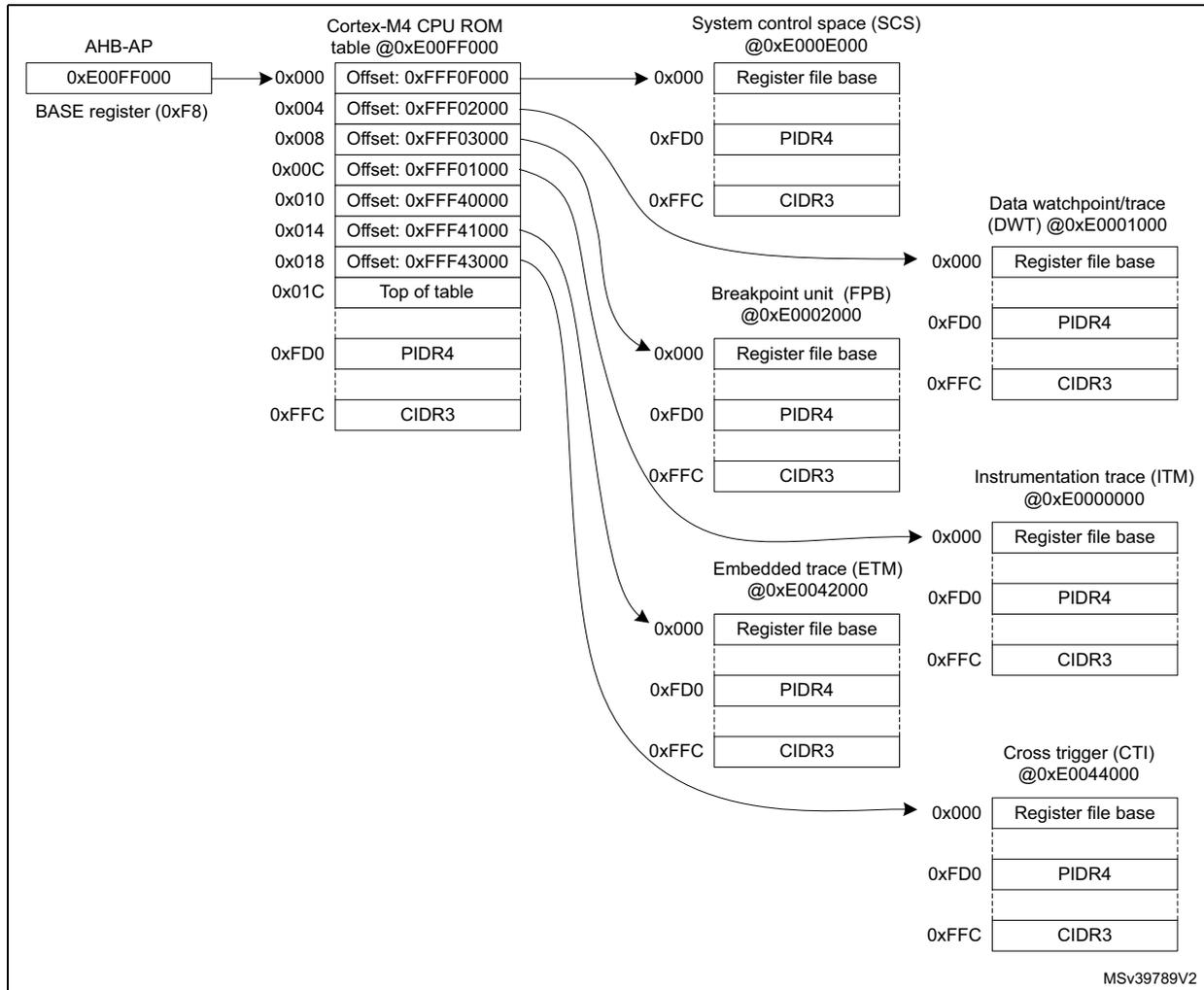
The diagram illustrates the CoreSight topology for Cortex-M4. It shows the following components and their connections:
- AHB-AP: Contains the BASE register (0xF8) at address 0xE00FF000. This register points to the Cortex-M4 CPU ROM table.
- Cortex-M4 CPU ROM table @0xE00FF000:
A table of pointers to various debug components.
- 0x000 Offset: 0xFFF0F000 points to System control space (SCS).
- 0x004 Offset: 0xFFF02000 points to Data watchpoint/trace (DWT).
- 0x008 Offset: 0xFFF03000 points to Breakpoint unit (FPB).
- 0x00C Offset: 0xFFF01000 points to Instrumentation trace (ITM).
- 0x010 Offset: 0xFFF40000 points to Embedded trace (ETM).
- 0x014 Offset: 0xFFF41000 points to Cross trigger (CTI).
- 0x018 Offset: 0xFFF43000.
- 0x01C Top of table.
- 0xFD0 PIDR4.
- 0xFFC CIDR3.
- System control space (SCS) @0xE000E000: Contains Register file base, PIDR4, and CIDR3.
- Data watchpoint/trace (DWT) @0xE0001000: Contains Register file base, PIDR4, and CIDR3.
- Breakpoint unit (FPB) @0xE0002000: Contains Register file base, PIDR4, and CIDR3.
- Instrumentation trace (ITM) @0xE0000000: Contains Register file base, PIDR4, and CIDR3.
- Embedded trace (ETM) @0xE0042000: Contains Register file base, PIDR4, and CIDR3.
- Cross trigger (CTI) @0xE0044000: Contains Register file base, PIDR4, and CIDR3.
MSv39789V2
Cortex-M4 ROM table registers
ROM memory type register (M4_ROM_MEMTYPE)
Address offset: 0xFCC
Reset value: 0x0000 0001
| 31 | 30 | 29 | 28 | 27 | 26 | 25 | 24 | 23 | 22 | 21 | 20 | 19 | 18 | 17 | 16 |
|---|---|---|---|---|---|---|---|---|---|---|---|---|---|---|---|
| Res. | Res. | Res. | Res. | Res. | Res. | Res. | Res. | Res. | Res. | Res. | Res. | Res. | Res. | Res. | Res. |
| 15 | 14 | 13 | 12 | 11 | 10 | 9 | 8 | 7 | 6 | 5 | 4 | 3 | 2 | 1 | 0 |
| Res. | Res. | Res. | Res. | Res. | Res. | Res. | Res. | Res. | Res. | Res. | Res. | Res. | Res. | Res. | SYSMEM |
| r | |||||||||||||||
Bits 31:1 Reserved, must be kept at reset value.
Bit 0 SYSTEM : System memory
1: System memory is present on this bus
ROM CoreSight peripheral identity register 4 (M4_ROM_PIDR4)
Address offset: 0xFD0
Reset value: 0x0000 0000
| 31 | 30 | 29 | 28 | 27 | 26 | 25 | 24 | 23 | 22 | 21 | 20 | 19 | 18 | 17 | 16 |
|---|---|---|---|---|---|---|---|---|---|---|---|---|---|---|---|
| Res. | Res. | Res. | Res. | Res. | Res. | Res. | Res. | Res. | Res. | Res. | Res. | Res. | Res. | Res. | Res. |
| 15 | 14 | 13 | 12 | 11 | 10 | 9 | 8 | 7 | 6 | 5 | 4 | 3 | 2 | 1 | 0 |
| Res. | Res. | Res. | Res. | Res. | Res. | Res. | Res. | 4KCOUNT[3:0] | JEP106CON[3:0] | ||||||
| r | r | r | r | r | r | r | r | ||||||||
Bits 31:8 Reserved, must be kept at reset value.
Bits 7:4 4KCOUNT[3:0] : Register file size
0x0: Register file occupies a single 4 Kbyte region
Bits 3:0 JEP106CON[3:0] : JEP106 continuation code
0x0: STMicroelectronics JEDEC continuation code
ROM CoreSight peripheral identity register 0 (M4_ROM_PIDR0)
Address offset: 0xFE0
Reset value: 0x0000 0050
| 31 | 30 | 29 | 28 | 27 | 26 | 25 | 24 | 23 | 22 | 21 | 20 | 19 | 18 | 17 | 16 |
|---|---|---|---|---|---|---|---|---|---|---|---|---|---|---|---|
| Res. | Res. | Res. | Res. | Res. | Res. | Res. | Res. | Res. | Res. | Res. | Res. | Res. | Res. | Res. | Res. |
| 15 | 14 | 13 | 12 | 11 | 10 | 9 | 8 | 7 | 6 | 5 | 4 | 3 | 2 | 1 | 0 |
| Res. | Res. | Res. | Res. | Res. | Res. | Res. | Res. | PARTNUM[7:0] | |||||||
| r | r | r | r | r | r | r | r | ||||||||
Bits 31:8 Reserved, must be kept at reset value.
Bits 7:0 PARTNUM[7:0] : Part number field, bits [7:0]
0x50: STM32H7
ROM CoreSight peripheral identity register 1 (M4_ROM_PIDR1)Address offset: 0xFE4
Reset value: 0x0000 0004
| 31 | 30 | 29 | 28 | 27 | 26 | 25 | 24 | 23 | 22 | 21 | 20 | 19 | 18 | 17 | 16 |
|---|---|---|---|---|---|---|---|---|---|---|---|---|---|---|---|
| Res. | Res. | Res. | Res. | Res. | Res. | Res. | Res. | Res. | Res. | Res. | Res. | Res. | Res. | Res. | Res. |
| 15 | 14 | 13 | 12 | 11 | 10 | 9 | 8 | 7 | 6 | 5 | 4 | 3 | 2 | 1 | 0 |
| Res. | Res. | Res. | Res. | Res. | Res. | Res. | Res. | JEP106ID[3:0] | PARTNUM[11:8] | ||||||
| r | r | r | r | r | r | r | r | ||||||||
Bits 31:8 Reserved, must be kept at reset value.
Bits 7:4 JEP106ID[3:0] : JEP106 identity code field, bits [3:0]0x0: STMicroelectronics JEDEC code
Bits 3:0 PARTNUM[11:8] : Part number field, bits [11:8]0x4: STM32H7
ROM CoreSight peripheral identity register 2 (M4_ROM_PIDR2)Address offset: 0xFE8
Reset value: 0x0000 000A
| 31 | 30 | 29 | 28 | 27 | 26 | 25 | 24 | 23 | 22 | 21 | 20 | 19 | 18 | 17 | 16 |
|---|---|---|---|---|---|---|---|---|---|---|---|---|---|---|---|
| Res. | Res. | Res. | Res. | Res. | Res. | Res. | Res. | Res. | Res. | Res. | Res. | Res. | Res. | Res. | Res. |
| 15 | 14 | 13 | 12 | 11 | 10 | 9 | 8 | 7 | 6 | 5 | 4 | 3 | 2 | 1 | 0 |
| Res. | Res. | Res. | Res. | Res. | Res. | Res. | Res. | REVISION[3:0] | JEDEC | JEP106ID[6:4] | |||||
| r | r | r | r | r | r | r | r | ||||||||
Bits 31:8 Reserved, must be kept at reset value.
Bits 7:4 REVISION[3:0] : Component revision number0x0: rev 0
Bit 3 JEDEC : JEDEC assigned value1: Designer ID specified by JEDEC
Bits 2:0 JEP106ID[6:4] : JEP106 identity code field, bits [6:4]0x2: STMicroelectronics JEDEC code
ROM CoreSight peripheral identity register 3 (M4_ROM_PIDR3)
Address offset: 0xFEC
Reset value: 0x0000 0000
| 31 | 30 | 29 | 28 | 27 | 26 | 25 | 24 | 23 | 22 | 21 | 20 | 19 | 18 | 17 | 16 |
|---|---|---|---|---|---|---|---|---|---|---|---|---|---|---|---|
| Res. | Res. | Res. | Res. | Res. | Res. | Res. | Res. | Res. | Res. | Res. | Res. | Res. | Res. | Res. | Res. |
| 15 | 14 | 13 | 12 | 11 | 10 | 9 | 8 | 7 | 6 | 5 | 4 | 3 | 2 | 1 | 0 |
| Res. | Res. | Res. | Res. | Res. | Res. | Res. | Res. | REVAND[3:0] | CMOD[3:0] | ||||||
| r | r | r | r | r | r | r | r | ||||||||
Bits 31:8 Reserved, must be kept at reset value.
Bits 7:4 REVAND[3:0] : Metal fix version
0x0: No metal fix
Bits 3:0 CMOD[3:0] : Customer modified
0x0: No customer modifications
ROM CoreSight component identity register 0 (M4_ROM_CIDR0)
Address offset: 0xFF0
Reset value: 0x0000 000D
| 31 | 30 | 29 | 28 | 27 | 26 | 25 | 24 | 23 | 22 | 21 | 20 | 19 | 18 | 17 | 16 |
|---|---|---|---|---|---|---|---|---|---|---|---|---|---|---|---|
| Res. | Res. | Res. | Res. | Res. | Res. | Res. | Res. | Res. | Res. | Res. | Res. | Res. | Res. | Res. | Res. |
| 15 | 14 | 13 | 12 | 11 | 10 | 9 | 8 | 7 | 6 | 5 | 4 | 3 | 2 | 1 | 0 |
| Res. | Res. | Res. | Res. | Res. | Res. | Res. | Res. | PREAMBLE[7:0] | |||||||
| r | r | r | r | r | r | r | r | ||||||||
Bits 31:8 Reserved, must be kept at reset value.
Bits 7:0 PREAMBLE[7:0] : Component ID field, bits [7:0]
0x0D: Common ID value
ROM CoreSight component identity register 1 (M4_ROM_CIDR1)
Address offset: 0xFF4
Reset value: 0x0000 0010
| 31 | 30 | 29 | 28 | 27 | 26 | 25 | 24 | 23 | 22 | 21 | 20 | 19 | 18 | 17 | 16 |
|---|---|---|---|---|---|---|---|---|---|---|---|---|---|---|---|
| Res. | Res. | Res. | Res. | Res. | Res. | Res. | Res. | Res. | Res. | Res. | Res. | Res. | Res. | Res. | Res. |
| 15 | 14 | 13 | 12 | 11 | 10 | 9 | 8 | 7 | 6 | 5 | 4 | 3 | 2 | 1 | 0 |
|---|---|---|---|---|---|---|---|---|---|---|---|---|---|---|---|
| Res. | Res. | Res. | Res. | Res. | Res. | Res. | Res. | CLASS[3:0] | PREAMBLE[11:8] | ||||||
| r | r | r | r | r | r | r | r | ||||||||
Bits 31:8 Reserved, must be kept at reset value.
Bits 7:4 CLASS[3:0] : Component ID field, bits [15:12] - component class
0x1: ROM table component
Bits 3:0 PREAMBLE[11:8] : Component ID field, bits [11:8]
0x0: Common ID value
ROM CoreSight component identity register 2 (M4_ROM_CIDR2)
Address offset: 0xFF8
Reset value: 0x0000 0005
| 31 | 30 | 29 | 28 | 27 | 26 | 25 | 24 | 23 | 22 | 21 | 20 | 19 | 18 | 17 | 16 |
|---|---|---|---|---|---|---|---|---|---|---|---|---|---|---|---|
| Res. | Res. | Res. | Res. | Res. | Res. | Res. | Res. | Res. | Res. | Res. | Res. | Res. | Res. | Res. | Res. |
| 15 | 14 | 13 | 12 | 11 | 10 | 9 | 8 | 7 | 6 | 5 | 4 | 3 | 2 | 1 | 0 |
| Res. | Res. | Res. | Res. | Res. | Res. | Res. | Res. | PREAMBLE[19:12] | |||||||
| r | r | r | r | r | r | r | r | ||||||||
Bits 31:8 Reserved, must be kept at reset value.
Bits 7:0 PREAMBLE[19:12] : Component ID field, bits [23:16]
0x05: Common ID value
ROM CoreSight component identity register 3 (M4_ROM_CIDR3)
Address offset: 0xFFC
Reset value: 0x0000 00B1
| 31 | 30 | 29 | 28 | 27 | 26 | 25 | 24 | 23 | 22 | 21 | 20 | 19 | 18 | 17 | 16 |
|---|---|---|---|---|---|---|---|---|---|---|---|---|---|---|---|
| Res. | Res. | Res. | Res. | Res. | Res. | Res. | Res. | Res. | Res. | Res. | Res. | Res. | Res. | Res. | Res. |
| 15 | 14 | 13 | 12 | 11 | 10 | 9 | 8 | 7 | 6 | 5 | 4 | 3 | 2 | 1 | 0 |
| Res. | Res. | Res. | Res. | Res. | Res. | Res. | Res. | PREAMBLE[27:20] | |||||||
| r | r | r | r | r | r | r | r | ||||||||
Bits 31:8 Reserved, must be kept at reset value.
Bits 7:0 PREAMBLE[27:20] : Component ID field, bits [31:24]
0xB1: Common ID value
Cortex-M4 ROM table register map and reset values
Table 652. Cortex-M4 ROM table register map and reset values
| Offset | Register name | 31 | 30 | 29 | 28 | 27 | 26 | 25 | 24 | 23 | 22 | 21 | 20 | 19 | 18 | 17 | 16 | 15 | 14 | 13 | 12 | 11 | 10 | 9 | 8 | 7 | 6 | 5 | 4 | 3 | 2 | 1 | 0 | |
|---|---|---|---|---|---|---|---|---|---|---|---|---|---|---|---|---|---|---|---|---|---|---|---|---|---|---|---|---|---|---|---|---|---|---|
| 0xFCC | M4_ROM_MEMTYPE | Res. | Res. | Res. | Res. | Res. | Res. | Res. | Res. | Res. | Res. | Res. | Res. | Res. | Res. | Res. | Res. | Res. | Res. | Res. | Res. | Res. | Res. | Res. | Res. | Res. | Res. | Res. | Res. | Res. | Res. | Res. | Res. | SYSTEM |
| Reset value | 1 | |||||||||||||||||||||||||||||||||
| 0xFD0 | M4_ROM_PIDR4 | Res. | Res. | Res. | Res. | Res. | Res. | Res. | Res. | Res. | Res. | Res. | Res. | Res. | Res. | Res. | Res. | Res. | Res. | Res. | Res. | Res. | Res. | Res. | Res. | 4KCOUNT[3:0] | JEP106CON[3:0] | |||||||
| Reset value | 0 | 0 | 0 | 0 | 0 | 0 | 0 | 0 | ||||||||||||||||||||||||||
| 0xFD4 to 0xFDC | Reserved | Reserved | ||||||||||||||||||||||||||||||||
| 0xFE0 | M4_ROM_PIDR0 | Res. | Res. | Res. | Res. | Res. | Res. | Res. | Res. | Res. | Res. | Res. | Res. | Res. | Res. | Res. | Res. | Res. | Res. | Res. | Res. | Res. | Res. | Res. | Res. | Res. | Res. | Res. | Res. | Res. | Res. | Res. | PARTNUM[7:0] | |
| Reset value | 0 1 0 1 0 0 0 0 | |||||||||||||||||||||||||||||||||
| 0xFE4 | M4_ROM_PIDR1 | Res. | Res. | Res. | Res. | Res. | Res. | Res. | Res. | Res. | Res. | Res. | Res. | Res. | Res. | Res. | Res. | Res. | Res. | Res. | Res. | Res. | Res. | Res. | Res. | Res. | Res. | Res. | Res. | Res. | Res. | Res. | JEP106ID[3:0] PARTNUM[11:8] | |
| Reset value | 0 0 0 0 0 0 1 0 0 | |||||||||||||||||||||||||||||||||
| 0xFE8 | M4_ROM_PIDR2 | Res. | Res. | Res. | Res. | Res. | Res. | Res. | Res. | Res. | Res. | Res. | Res. | Res. | Res. | Res. | Res. | Res. | Res. | Res. | Res. | Res. | Res. | Res. | Res. | Res. | Res. | Res. | Res. | Res. | Res. | Res. | REVISION[3:0] JEDEC JEP106ID[6:4] | |
| Reset value | 0 0 0 0 1 0 1 0 | |||||||||||||||||||||||||||||||||
| 0xFEC | M4_ROM_PIDR3 | Res. | Res. | Res. | Res. | Res. | Res. | Res. | Res. | Res. | Res. | Res. | Res. | Res. | Res. | Res. | Res. | Res. | Res. | Res. | Res. | Res. | Res. | Res. | Res. | Res. | Res. | Res. | Res. | Res. | Res. | Res. | REVAND[3:0] CMOD[3:0] | |
| Reset value | 0 0 0 0 0 0 0 0 | |||||||||||||||||||||||||||||||||
| 0xFF0 | M4_ROM_CIDR0 | Res. | Res. | Res. | Res. | Res. | Res. | Res. | Res. | Res. | Res. | Res. | Res. | Res. | Res. | Res. | Res. | Res. | Res. | Res. | Res. | Res. | Res. | Res. | Res. | Res. | Res. | Res. | Res. | Res. | Res. | Res. | PREAMBLE[7:0] | |
| Reset value | 0 0 0 0 0 1 1 0 1 | |||||||||||||||||||||||||||||||||
| 0xFF4 | M4_ROM_CIDR1 | Res. | Res. | Res. | Res. | Res. | Res. | Res. | Res. | Res. | Res. | Res. | Res. | Res. | Res. | Res. | Res. | Res. | Res. | Res. | Res. | Res. | Res. | Res. | Res. | Res. | Res. | Res. | Res. | Res. | Res. | Res. | CLASS[3:0] PREAMBLE[11:8] | |
| Reset value | 0 0 0 1 1 0 0 0 0 | |||||||||||||||||||||||||||||||||
| 0xFF8 | M4_ROM_CIDR2 | Res. | Res. | Res. | Res. | Res. | Res. | Res. | Res. | Res. | Res. | Res. | Res. | Res. | Res. | Res. | Res. | Res. | Res. | Res. | Res. | Res. | Res. | Res. | Res. | Res. | Res. | Res. | Res. | Res. | Res. | Res. | PREAMBLE[19:12] | |
| Reset value | 0 0 0 0 0 0 1 0 1 | |||||||||||||||||||||||||||||||||
| 0xFFC | M4_ROM_CIDR3 | Res. | Res. | Res. | Res. | Res. | Res. | Res. | Res. | Res. | Res. | Res. | Res. | Res. | Res. | Res. | Res. | Res. | Res. | Res. | Res. | Res. | Res. | Res. | Res. | Res. | Res. | Res. | Res. | Res. | Res. | Res. | PREAMBLE[27:20] | |
| Reset value | 1 0 1 1 1 0 0 0 1 | |||||||||||||||||||||||||||||||||
63.7.2 Cortex-M4 data watchpoint and trace unit (DWT)
The DWT provides four comparators that can be used as:
- • watchpoint
- • ETM trigger
- • PC sampling trigger
- • data address sampling trigger
- • data comparator (comparator 1 only)
- • clock cycle counter comparator (comparator 0 only)
It also contains counters for:
- • clock cycles
- • folded instructions
- • load store unit (LSU) operations
- • sleep cycles
- • number of cycles per instruction
- • interrupt overhead
A DWT comparator compares one of the following with the value held in its DWT_COMP register:
- • a data address
- • an instruction address
- • a data value
- • the cycle count value, for comparator 0 only.
For address matching, the comparator can use a mask, so it matches a range of addresses.
On a successful match, the comparator generates one of the following:
- • one or more DWT Data trace packets, containing one or more of:
- – the address of the instruction that caused a data access
- – an address offset, bits[15:0] of the data access address
- – the matched data value
- • a watchpoint debug event, on either the PC value or the accessed data address
- • a CMPMATCH[N] event, that signals the match outside the DWT unit
A watchpoint debug event either generates a DebugMonitor exception, or causes the processor to halt execution and enter Debug state.
For more details on how to use the DWT, refer to the Arm ® v7-M Architecture Reference Manual [5].
Cortex-M4 DWT registers
DWT control register (M4_DWT_CTRL)
Address offset: 0x000
Reset value: 0x4000 0000
| 31 | 30 | 29 | 28 | 27 | 26 | 25 | 24 | 23 | 22 | 21 | 20 | 19 | 18 | 17 | 16 |
|---|---|---|---|---|---|---|---|---|---|---|---|---|---|---|---|
| NUMCOMP[3:0]. | NOTR CPKT | NOEX TTRIG | NOCYC CNT | NOPRF CNT | Res. | CYCEV TENA | FOLDE VTENA | LSUEV TENA | SLEEP EVTEN A | EXCEV TENA | CPIEVT ENA | EXCTR CENA | |||
| r | r | r | r | r | r | r | r | rw | rw | rw | rw | rw | rw | rw | |
| 15 | 14 | 13 | 12 | 11 | 10 | 9 | 8 | 7 | 6 | 5 | 4 | 3 | 2 | 1 | 0 |
| Res. | Res. | Res. | PCSA MPLE NA | SYNCTAP[1:0] | CYCTA P | POSTINIT[3:0] | POSTRESET[3:0] | CYCCN TENA | |||||||
| rw | rw | rw | rw | rw | rw | rw | rw | rw | rw | rw | rw | rw | |||
Bits 31:28 NUMCOMP[3:0] : Number of comparators implemented (read-only)
0x4: Four comparators
Bit 27 NOTRCPKT : Trace sampling and exception tracing support (read-only)
0: Supported
Bit 26 NOEXTTRIG : External match signal, CMPMATCH support (read-only)
0: Supported
Bit 25 NOCYCCNT : Cycle counter support (read-only)
0: Supported
Bit 24 NOPRFCNT : Profiling counter support (read-only)
0: Supported
Bit 23 Reserved, must be kept at reset value.
Bit 22 CYCEVTENA : Enable for POSTCNT underflow event counter packet generation
0: Disabled
1: Enabled
Bit 21 FOLDEVVTENA : Enable for folded instruction counter overflow event generation
0: Disabled
1: Enabled
Bit 20 LSUEVTENA : Enable for LSU counter overflow event generation
0: Disabled
1: Enabled
Bit 19 SLEEPEVTENA : Enable for sleep counter overflow event generation
0: Disabled
1: Enabled
Bit 18 EXCEVTENA : Enable for exception overhead counter overflow event generation
0: Disabled
1: Enabled
Bit 17 CPIEVTENA : Enable for CPI counter overflow event generation
0: Disabled
1: Enabled
Bit 16 EXCTRCENA : Enable for exception trace generation
0: Disabled
1: Enabled
Bits 15:13 Reserved, must be kept at reset value.
Bit 12 PCSAMPLENA : Enable for POSTCNT use as sample timer
Enables use of POSTCNT counter as a timer for Periodic PC sample packet generation.
0: Disabled
1: Enabled
Bits 11:10 SYNCTAP[1:0] : Position of sync packet counter tap on CYCCNT
Selects the position of the synchronization packet counter tap on the CYCCNT counter. This determines the synchronization packet rate.
0x0: Disabled. No synchronization packets
0x1: Tap at CYCCNT[24]
0x2: Tap at CYCCNT[26]
0x3: Tap at CYCCNT[28]
Bit 9 CYCTAP : Position of POSTCNT tap on CYCCNT
Selects the position of the POSTCNT tap on the CYCCNT counter.
0: Tap at CYCCNT[6]
1: Tap at CYCCNT[10]
Bits 8:5 POSTINIT[3:0] : Initial value of POSTCNT
Writes to this field are ignored if POSTCNT counter is enabled (that is, CYCEVTENA or PCSAMPLENA must be reset prior to writing POSTINIT).
Bits 4:1 POSTRESET[3:0] : Reload value of the POSTCNT counter
Bit 0 CYCCNTENA : CYCCNT counter enable
0: Disabled
1: Enabled
DWT cycle count register (M4_DWT_CYCCNT)
Address offset: 0x004
Reset value: 0x0000 0000
| 31 | 30 | 29 | 28 | 27 | 26 | 25 | 24 | 23 | 22 | 21 | 20 | 19 | 18 | 17 | 16 |
|---|---|---|---|---|---|---|---|---|---|---|---|---|---|---|---|
| CYCCNT[31:16] | |||||||||||||||
| rw | rw | rw | rw | rw | rw | rw | rw | rw | rw | rw | rw | rw | rw | rw | rw |
| 15 | 14 | 13 | 12 | 11 | 10 | 9 | 8 | 7 | 6 | 5 | 4 | 3 | 2 | 1 | 0 |
| CYCCNT[15:0] | |||||||||||||||
| rw | rw | rw | rw | rw | rw | rw | rw | rw | rw | rw | rw | rw | rw | rw | rw |
Bits 31:0 CYCCNT[31:0] : Processor clock cycle counter
DWT CPI count register (M4_DWT_CPICNT)
Address offset: 0x008
Reset value: 0x0000 0000
| 31 | 30 | 29 | 28 | 27 | 26 | 25 | 24 | 23 | 22 | 21 | 20 | 19 | 18 | 17 | 16 |
|---|---|---|---|---|---|---|---|---|---|---|---|---|---|---|---|
| Res. | Res. | Res. | Res. | Res. | Res. | Res. | Res. | Res. | Res. | Res. | Res. | Res. | Res. | Res. | Res. |
| 15 | 14 | 13 | 12 | 11 | 10 | 9 | 8 | 7 | 6 | 5 | 4 | 3 | 2 | 1 | 0 |
| Res. | Res. | Res. | Res. | Res. | Res. | Res. | Res. | CPICNT[7:0] | |||||||
| rw | rw | rw | rw | rw | rw | rw | rw | ||||||||
Bits 31:8 Reserved, must be kept at reset value.
Bits 7:0 CPICNT[7:0] : CPI counter
Counts additional cycles required to execute multi-cycle instructions, except those recorded by M4_DWT_LSUCNT, and counts any instruction fetch stalls.
DWT exception count register (M4_DWT_EXCCNT)
Address offset: 0x00C
Reset value: 0x0000 0000
| 31 | 30 | 29 | 28 | 27 | 26 | 25 | 24 | 23 | 22 | 21 | 20 | 19 | 18 | 17 | 16 |
|---|---|---|---|---|---|---|---|---|---|---|---|---|---|---|---|
| Res. | Res. | Res. | Res. | Res. | Res. | Res. | Res. | Res. | Res. | Res. | Res. | Res. | Res. | Res. | Res. |
| 15 | 14 | 13 | 12 | 11 | 10 | 9 | 8 | 7 | 6 | 5 | 4 | 3 | 2 | 1 | 0 |
| Res. | Res. | Res. | Res. | Res. | Res. | Res. | Res. | EXCCNT[7:0] | |||||||
| rw | rw | rw | rw | rw | rw | rw | rw | ||||||||
Bits 31:8 Reserved, must be kept at reset value.
Bits 7:0 EXCCNT[7:0] : Exception overhead cycle counter
Counts the number of cycles spent in exception processing.
DWT sleep count register (M4_DWT_SLPCNT)
Address offset: 0x010
Reset value: 0x0000 0000
| 31 | 30 | 29 | 28 | 27 | 26 | 25 | 24 | 23 | 22 | 21 | 20 | 19 | 18 | 17 | 16 |
|---|---|---|---|---|---|---|---|---|---|---|---|---|---|---|---|
| Res. | Res. | Res. | Res. | Res. | Res. | Res. | Res. | Res. | Res. | Res. | Res. | Res. | Res. | Res. | Res. |
| 15 | 14 | 13 | 12 | 11 | 10 | 9 | 8 | 7 | 6 | 5 | 4 | 3 | 2 | 1 | 0 |
| Res. | Res. | Res. | Res. | Res. | Res. | Res. | Res. | SLEEPCNT[7:0] | |||||||
| rw | rw | rw | rw | rw | rw | rw | rw | ||||||||
Bits 31:8 Reserved, must be kept at reset value.
Bits 7:0 SLEEPCNT[7:0] : Sleep cycle counter
Counts the number of cycles spent in sleep mode (WFI, WFE, sleep-on-exit).
DWT LSU count register (M4_DWT_LSUCNT)
Address offset: 0x014
Reset value: 0x0000 0000
| 31 | 30 | 29 | 28 | 27 | 26 | 25 | 24 | 23 | 22 | 21 | 20 | 19 | 18 | 17 | 16 |
|---|---|---|---|---|---|---|---|---|---|---|---|---|---|---|---|
| Res. | Res. | Res. | Res. | Res. | Res. | Res. | Res. | Res. | Res. | Res. | Res. | Res. | Res. | Res. | Res. |
| 15 | 14 | 13 | 12 | 11 | 10 | 9 | 8 | 7 | 6 | 5 | 4 | 3 | 2 | 1 | 0 |
|---|---|---|---|---|---|---|---|---|---|---|---|---|---|---|---|
| Res. | Res. | Res. | Res. | Res. | Res. | Res. | Res. | LSUCNT[7:0] | |||||||
| rw | rw | rw | rw | rw | rw | rw | rw | ||||||||
Bits 31:8 Reserved, must be kept at reset value.
Bits 7:0 LSUCNT[7:0] : Load store counter
Counts additional cycles required to execute load and store instructions.
DWT fold count register (M4_DWT_FOLDCNT)
Address offset: 0x018
Reset value: 0x0000 0000
| 31 | 30 | 29 | 28 | 27 | 26 | 25 | 24 | 23 | 22 | 21 | 20 | 19 | 18 | 17 | 16 |
|---|---|---|---|---|---|---|---|---|---|---|---|---|---|---|---|
| Res. | Res. | Res. | Res. | Res. | Res. | Res. | Res. | Res. | Res. | Res. | Res. | Res. | Res. | Res. | Res. |
| 15 | 14 | 13 | 12 | 11 | 10 | 9 | 8 | 7 | 6 | 5 | 4 | 3 | 2 | 1 | 0 |
| Res. | Res. | Res. | Res. | Res. | Res. | Res. | Res. | FOLDCNT[7:0] | |||||||
| rw | rw | rw | rw | rw | rw | rw | rw | ||||||||
Bits 31:8 Reserved, must be kept at reset value.
Bits 7:0 FOLDCNT[7:0] : Folded instruction counter
Increments on each instruction that takes 0 cycles.
DWT program counter sample register (M4_DWT_PCSR)
Address offset: 0x01C
Reset value: 0x0000 0000
| 31 | 30 | 29 | 28 | 27 | 26 | 25 | 24 | 23 | 22 | 21 | 20 | 19 | 18 | 17 | 16 |
|---|---|---|---|---|---|---|---|---|---|---|---|---|---|---|---|
| EIASAMPLE[31:16] | |||||||||||||||
| rw | rw | rw | rw | rw | rw | rw | rw | rw | rw | rw | rw | rw | rw | rw | rw |
| 15 | 14 | 13 | 12 | 11 | 10 | 9 | 8 | 7 | 6 | 5 | 4 | 3 | 2 | 1 | 0 |
| EIASAMPLE[15:0] | |||||||||||||||
| rw | rw | rw | rw | rw | rw | rw | rw | rw | rw | rw | rw | rw | rw | rw | rw |
Bits 31:0 EIASAMPLE[31:0] : Executed instruction address sample value
Samples the current value of the program counter.
DWT comparator register x (M4_DWT_COMPx)
Address offset: 0x020 + x * 0x10 (for x = 0 to 3)
Reset value: 0x0000 0000
| 31 | 30 | 29 | 28 | 27 | 26 | 25 | 24 | 23 | 22 | 21 | 20 | 19 | 18 | 17 | 16 |
| COMP[31:16] | |||||||||||||||
| rw | rw | rw | rw | rw | rw | rw | rw | rw | rw | rw | rw | rw | rw | rw | rw |
| 15 | 14 | 13 | 12 | 11 | 10 | 9 | 8 | 7 | 6 | 5 | 4 | 3 | 2 | 1 | 0 |
| COMP[15:0] | |||||||||||||||
| rw | rw | rw | rw | rw | rw | rw | rw | rw | rw | rw | rw | rw | rw | rw | rw |
Bits 31:0 COMP[31:0] : Reference value for comparison
DWT mask register x (M4_DWT_MASKx)
Address offset: 0x024 + x * 0x10 (for x = 0 to 3)
Reset value: 0x0000 0000
| 31 | 30 | 29 | 28 | 27 | 26 | 25 | 24 | 23 | 22 | 21 | 20 | 19 | 18 | 17 | 16 |
| Res. | Res. | Res. | Res. | Res. | Res. | Res. | Res. | Res. | Res. | Res. | Res. | Res. | Res. | Res. | Res. |
| 15 | 14 | 13 | 12 | 11 | 10 | 9 | 8 | 7 | 6 | 5 | 4 | 3 | 2 | 1 | 0 |
| Res. | Res. | Res. | Res. | Res. | Res. | Res. | Res. | Res. | Res. | Res. | MASK[4:0] | ||||
| rw | rw | rw | rw | rw | |||||||||||
Bits 31:5 Reserved, must be kept at reset value.
Bits 4:0 MASK[4:0] : Comparator mask size
Provides the size of the ignore mask applied to the access address for address range matching by comparator n. A debugger can write 0b11111 to this field and then read the register back to determine the maximum mask size supported.
DWT function register x (M4_DWT_FUNCTx)
Address offset: 0x028 + x * 0x10 (for x = 0 to 3)
Reset value: 0x0000 0000
| 31 | 30 | 29 | 28 | 27 | 26 | 25 | 24 | 23 | 22 | 21 | 20 | 19 | 18 | 17 | 16 |
| Res. | Res. | Res. | Res. | Res. | Res. | Res. | MATCH ED | Res. | Res. | Res. | Res. | DATAVADDR1[3:0] | |||
| r | rw | rw | rw | rw | |||||||||||
| 15 | 14 | 13 | 12 | 11 | 10 | 9 | 8 | 7 | 6 | 5 | 4 | 3 | 2 | 1 | 0 |
| DATAVADDR0[3:0] | DATAVSIZE[1:0] | LINK1 ENA | DATAV MATCH | CYC MATCH | Res. | EMIT RANGE | Res. | FUNCTION[3:0] | |||||||
| rw | rw | rw | rw | rw | rw | rw | rw | rw | rw | rw | rw | rw | rw | ||
Bits 31:25 Reserved, must be kept at reset value.
Bit 24 MATCHED : Comparator match (read-only)
Indicates if a comparator match has occurred since the register was last read.
0: No match
1: Match occurred
Bits 23:20 Reserved, must be kept at reset value.
Bits 19:16 DATAVADDR1[3:0] : Comparator number of a second comparator
When the DATAVMATCH and LNK1ENA bits are both 1, this field can hold the comparator number of a second comparator to use for linked address comparison.
Bits 15:12 DATAVADDR0[3:0] : Comparator number of a comparator
When the DATAVMATCH and LNK1ENA bits are both 1, this field can hold the comparator number of a comparator to use for linked address comparison.
Bits 11:10 DATAVSIZE[1:0] : Size of required data comparison
For data value matching, specifies the size of the required data comparison.
0x0: Byte
0x1: Half word
0x2: Word
0x3: Reserved
Bit 9 LNK1ENA : Support of a second linked comparator (read-only)
Indicates whether use of a second linked comparator is supported (read-only).
1: Supported
Bit 8 DATAVMATCH : Cycle comparison enable
0: Perform address comparison
1: Perform data value comparison
Bit 7 CYCMATCH : Enables cycle count comparison on comparator 0. This field is reserved for other comparators.
0: No cycle count comparison
1: Compare M4_DWT_COMP0 with the cycle counter, M4_DWT_CYCCNT
Bit 6 Reserved, must be kept at reset value
Bit 5 EMITRANGE : Data trace address offset packet enable
Enables generation of data trace address offset packets (containing data address bits 0 to 15)
0: Disabled
1: Enabled
Bit 4 Reserved, must be kept at reset value.
Bits 3:0 FUNCTION[3:0] : Action on comparator match
The meaning of this bit field depends on the setting of the DATAVMATCH and CYCMATCH fields. See [5].
DWT CoreSight peripheral identity register 4 (M4_DWT_PIDR4)
Address offset: 0xFD0
Reset value: 0x0000 0004
| 31 | 30 | 29 | 28 | 27 | 26 | 25 | 24 | 23 | 22 | 21 | 20 | 19 | 18 | 17 | 16 |
|---|---|---|---|---|---|---|---|---|---|---|---|---|---|---|---|
| Res. | Res. | Res. | Res. | Res. | Res. | Res. | Res. | Res. | Res. | Res. | Res. | Res. | Res. | Res. | Res. |
| 15 | 14 | 13 | 12 | 11 | 10 | 9 | 8 | 7 | 6 | 5 | 4 | 3 | 2 | 1 | 0 |
| Res. | Res. | Res. | Res. | Res. | Res. | Res. | Res. | 4KCOUNT[3:0] | JEP106CON[3:0] | ||||||
| r | r | r | r | r | r | r | r | ||||||||
Bits 31:8 Reserved, must be kept at reset value.
Bits 7:4 4KCOUNT[3:0] : Register file size
0x0: Register file occupies a single 4 Kbyte region
Bits 3:0 JEP106CON[3:0] : JEP106 continuation code
0x4: Arm ® JEDEC code
DWT CoreSight peripheral identity register 0 (M4_DWT_PIDR0)
Address offset: 0xFE0
Reset value: 0x0000 0002
| 31 | 30 | 29 | 28 | 27 | 26 | 25 | 24 | 23 | 22 | 21 | 20 | 19 | 18 | 17 | 16 |
|---|---|---|---|---|---|---|---|---|---|---|---|---|---|---|---|
| Res. | Res. | Res. | Res. | Res. | Res. | Res. | Res. | Res. | Res. | Res. | Res. | Res. | Res. | Res. | Res. |
| 15 | 14 | 13 | 12 | 11 | 10 | 9 | 8 | 7 | 6 | 5 | 4 | 3 | 2 | 1 | 0 |
| Res. | Res. | Res. | Res. | Res. | Res. | Res. | Res. | PARTNUM[7:0] | |||||||
| r | r | ||||||||||||||
Bits 31:8 Reserved, must be kept at reset value.
Bits 7:0 PARTNUM[7:0] : Part number field, bits [7:0]
0x02: DWT part number
DWT CoreSight peripheral identity register 1 (M4_DWT_PIDR1)
Address offset: 0xFE4
Reset value: 0x0000 00B0
| 31 | 30 | 29 | 28 | 27 | 26 | 25 | 24 | 23 | 22 | 21 | 20 | 19 | 18 | 17 | 16 |
|---|---|---|---|---|---|---|---|---|---|---|---|---|---|---|---|
| Res. | Res. | Res. | Res. | Res. | Res. | Res. | Res. | Res. | Res. | Res. | Res. | Res. | Res. | Res. | Res. |
| 15 | 14 | 13 | 12 | 11 | 10 | 9 | 8 | 7 | 6 | 5 | 4 | 3 | 2 | 1 | 0 |
|---|---|---|---|---|---|---|---|---|---|---|---|---|---|---|---|
| Res. | Res. | Res. | Res. | Res. | Res. | Res. | Res. | JEP106ID[3:0] | PARTNUM[11:8] | ||||||
| r | r | r | r | r | r | r | r | ||||||||
Bits 31:8 Reserved, must be kept at reset value.
Bits 7:4 JEP106ID[3:0] : JEP106 identity code field, bits [3:0]
0xB: Arm ® JEDEC code
Bits 3:0 PARTNUM[11:8] : Part number field, bits [11:8]
0x0: DWT part number
DWT CoreSight peripheral identity register 2 (M4_DWT_PIDR2)
Address offset: 0xFE8
Reset value: 0x0000 003B
| 31 | 30 | 29 | 28 | 27 | 26 | 25 | 24 | 23 | 22 | 21 | 20 | 19 | 18 | 17 | 16 |
|---|---|---|---|---|---|---|---|---|---|---|---|---|---|---|---|
| Res. | Res. | Res. | Res. | Res. | Res. | Res. | Res. | Res. | Res. | Res. | Res. | Res. | Res. | Res. | Res. |
| 15 | 14 | 13 | 12 | 11 | 10 | 9 | 8 | 7 | 6 | 5 | 4 | 3 | 2 | 1 | 0 |
| Res. | Res. | Res. | Res. | Res. | Res. | Res. | Res. | REVISION[3:0] | JEDEC | JEP106ID[6:4] | |||||
| r | r | r | r | r | r | r | r | ||||||||
Bits 31:8 Reserved, must be kept at reset value.
Bits 7:4 REVISION[3:0] : Component revision number
0x3: r0p4
Bit 3 JEDEC : JEDEC assigned value
1: Designer ID specified by JEDEC
Bits 2:0 JEP106ID[6:4] : JEP106 identity code field, bits [6:4]
0x3: Arm ® JEDEC code
DWT CoreSight peripheral identity register 3 (M4_DWT_PIDR3)
Address offset: 0xFEC
Reset value: 0x0000 0000
| 31 | 30 | 29 | 28 | 27 | 26 | 25 | 24 | 23 | 22 | 21 | 20 | 19 | 18 | 17 | 16 |
|---|---|---|---|---|---|---|---|---|---|---|---|---|---|---|---|
| Res. | Res. | Res. | Res. | Res. | Res. | Res. | Res. | Res. | Res. | Res. | Res. | Res. | Res. | Res. | Res. |
| 15 | 14 | 13 | 12 | 11 | 10 | 9 | 8 | 7 | 6 | 5 | 4 | 3 | 2 | 1 | 0 |
| Res. | Res. | Res. | Res. | Res. | Res. | Res. | Res. | REVAND[3:0] | CMOD[3:0] | ||||||
| r | r | r | r | r | r | r | r | ||||||||
Bits 31:8 Reserved, must be kept at reset value.
Bits 7:4 REVAND[3:0] : Metal fix version
0x0: No metal fix
Bits 3:0 CMOD[3:0] : Customer modified
0x0: No customer modifications
DWT CoreSight component identity register 0 (M4_DWT_CIDR0)
Address offset: 0xFF0
Reset value: 0x0000 000D
| 31 | 30 | 29 | 28 | 27 | 26 | 25 | 24 | 23 | 22 | 21 | 20 | 19 | 18 | 17 | 16 |
|---|---|---|---|---|---|---|---|---|---|---|---|---|---|---|---|
| Res. | Res. | Res. | Res. | Res. | Res. | Res. | Res. | Res. | Res. | Res. | Res. | Res. | Res. | Res. | Res. |
| 15 | 14 | 13 | 12 | 11 | 10 | 9 | 8 | 7 | 6 | 5 | 4 | 3 | 2 | 1 | 0 |
| Res. | Res. | Res. | Res. | Res. | Res. | Res. | Res. | PREAMBLE[7:0] | |||||||
| r | r | r | r | r | r | r | r | ||||||||
Bits 31:8 Reserved, must be kept at reset value.
Bits 7:0 PREAMBLE[7:0] : Component ID field, bits [7:0]
0x0D: Common ID value
DWT CoreSight component identity register 1 (M4_DWT_CIDR1)
Address offset: 0xFF4
Reset value: 0x0000 00E0
| 31 | 30 | 29 | 28 | 27 | 26 | 25 | 24 | 23 | 22 | 21 | 20 | 19 | 18 | 17 | 16 |
|---|---|---|---|---|---|---|---|---|---|---|---|---|---|---|---|
| Res. | Res. | Res. | Res. | Res. | Res. | Res. | Res. | Res. | Res. | Res. | Res. | Res. | Res. | Res. | Res. |
| 15 | 14 | 13 | 12 | 11 | 10 | 9 | 8 | 7 | 6 | 5 | 4 | 3 | 2 | 1 | 0 |
| Res. | Res. | Res. | Res. | Res. | Res. | Res. | Res. | CLASS[3:0] | PREAMBLE[11:8] | ||||||
| r | r | r | r | r | r | r | r | ||||||||
Bits 31:8 Reserved, must be kept at reset value.
Bits 7:4 CLASS[3:0] : Component ID field, bits [15:12] - component class
0xE: Trace generator component
Bits 3:0 PREAMBLE[11:8] : Component ID field, bits [11:8]
0x0: Common ID value
DWT CoreSight component identity register 2 (M4_DWT_CIDR2)
Address offset: 0xFF8
Reset value: 0x0000 0005
| 31 | 30 | 29 | 28 | 27 | 26 | 25 | 24 | 23 | 22 | 21 | 20 | 19 | 18 | 17 | 16 |
|---|---|---|---|---|---|---|---|---|---|---|---|---|---|---|---|
| Res. | Res. | Res. | Res. | Res. | Res. | Res. | Res. | Res. | Res. | Res. | Res. | Res. | Res. | Res. | Res. |
| 15 | 14 | 13 | 12 | 11 | 10 | 9 | 8 | 7 | 6 | 5 | 4 | 3 | 2 | 1 | 0 |
| Res. | Res. | Res. | Res. | Res. | Res. | Res. | Res. | PREAMBLE[19:12] | |||||||
| r | r | r | r | r | r | r | r | ||||||||
Bits 31:8 Reserved, must be kept at reset value.
Bits 7:0 PREAMBLE[19:12] : Component ID field, bits [23:16]
0x05: Common ID value
DWT CoreSight component identity register 3 (M4_DWT_CIDR3)
Address offset: 0xFFC
Reset value: 0x0000 00B1
| 31 | 30 | 29 | 28 | 27 | 26 | 25 | 24 | 23 | 22 | 21 | 20 | 19 | 18 | 17 | 16 |
|---|---|---|---|---|---|---|---|---|---|---|---|---|---|---|---|
| Res. | Res. | Res. | Res. | Res. | Res. | Res. | Res. | Res. | Res. | Res. | Res. | Res. | Res. | Res. | Res. |
| 15 | 14 | 13 | 12 | 11 | 10 | 9 | 8 | 7 | 6 | 5 | 4 | 3 | 2 | 1 | 0 |
| Res. | Res. | Res. | Res. | Res. | Res. | Res. | Res. | PREAMBLE[27:20] | |||||||
| r | r | r | r | r | r | r | r | ||||||||
Bits 31:8 Reserved, must be kept at reset value.
Bits 7:0 PREAMBLE[27:20] : Component ID field, bits [31:24]
0xB1: Common ID value
Cortex-M4 DWT register map and reset values
The Cortex-M4 DWT registers are located at address range 0xE0001000 to 0xE0001FFC.
Table 653. Cortex-M4 DWT register map and reset values
| Offset | Register name | 31 | 30 | 29 | 28 | 27 | 26 | 25 | 24 | 23 | 22 | 21 | 20 | 19 | 18 | 17 | 16 | 15 | 14 | 13 | 12 | 11 | 10 | 9 | 8 | 7 | 6 | 5 | 4 | 3 | 2 | 1 | 0 |
|---|---|---|---|---|---|---|---|---|---|---|---|---|---|---|---|---|---|---|---|---|---|---|---|---|---|---|---|---|---|---|---|---|---|
| 0x000 | M4_DWT_CTRL | NUMCOMP[3:0] | NOTRCPKT | NOEXTTRIG | NOCYCCNT | NOPRFCNT | Res. | CYCEVTENA | FOLDEVTENA | LSUEVTENA | SLEEPEVTENA | EXCEVTENA | CPIEVTENA | EXCTRCENA | Res. | Res. | Res. | PCSAMPLENA | SYNCTAP[1:0] | CYCTAP | Res. | POSINIT[3:0] | POSTPRESET[3:0] | CYCCNTENA | |||||||||
| 0 | 1 | 0 | 0 | 0 | 0 | 0 | 0 | 0 | 0 | 0 | 0 | 0 | 0 | 0 | 0 | 0 | 0 | 0 | 0 | 0 | 0 | 0 | 0 | 0 | 0 | 0 | 0 | ||||||
Table 653. Cortex-M4 DWT register map and reset values (continued)
| Offset | Register name | 31 | 30 | 29 | 28 | 27 | 26 | 25 | 24 | 23 | 22 | 21 | 20 | 19 | 18 | 17 | 16 | 15 | 14 | 13 | 12 | 11 | 10 | 9 | 8 | 7 | 6 | 5 | 4 | 3 | 2 | 1 | 0 |
|---|---|---|---|---|---|---|---|---|---|---|---|---|---|---|---|---|---|---|---|---|---|---|---|---|---|---|---|---|---|---|---|---|---|
| 0x004 | M4_DWT_CYCCNT | CYCCNT[31:0] | |||||||||||||||||||||||||||||||
| Reset value | 0 | 0 | 0 | 0 | 0 | 0 | 0 | 0 | 0 | 0 | 0 | 0 | 0 | 0 | 0 | 0 | 0 | 0 | 0 | 0 | 0 | 0 | 0 | 0 | 0 | 0 | 0 | 0 | 0 | 0 | 0 | 0 | |
| 0x008 | M4_DWT_CPICNT | Res | Res | Res | Res | Res | Res | Res | Res | Res | Res | Res | Res | Res | Res | Res | Res | Res | Res | Res | Res | Res | Res | Res | Res | CPICNT[7:0] | |||||||
| Reset value | 0 | 0 | 0 | 0 | 0 | 0 | 0 | 0 | |||||||||||||||||||||||||
| 0x00C | M4_DWT_EXCCNT | Res | Res | Res | Res | Res | Res | Res | Res | Res | Res | Res | Res | Res | Res | Res | Res | Res | Res | Res | Res | Res | Res | Res | Res | EXCCNT[7:0] | |||||||
| Reset value | 0 | 0 | 0 | 0 | 0 | 0 | 0 | 0 | |||||||||||||||||||||||||
| 0x010 | M4_DWT_SLP CNT | Res | Res | Res | Res | Res | Res | Res | Res | Res | Res | Res | Res | Res | Res | Res | Res | Res | Res | Res | Res | Res | Res | Res | Res | SLP CNT[7:0] | |||||||
| Reset value | 0 | 0 | 0 | 0 | 0 | 0 | 0 | 0 | |||||||||||||||||||||||||
| 0x014 | M4_DWT_LSUCNT | Res | Res | Res | Res | Res | Res | Res | Res | Res | Res | Res | Res | Res | Res | Res | Res | Res | Res | Res | Res | Res | Res | Res | Res | LSUCNT[7:0] | |||||||
| Reset value | 0 | 0 | 0 | 0 | 0 | 0 | 0 | 0 | |||||||||||||||||||||||||
| 0x018 | M4_DWT_FOLDCNT | Res | Res | Res | Res | Res | Res | Res | Res | Res | Res | Res | Res | Res | Res | Res | Res | Res | Res | Res | Res | Res | Res | Res | Res | FOLDCNT[7:0] | |||||||
| Reset value | 0 | 0 | 0 | 0 | 0 | 0 | 0 | 0 | |||||||||||||||||||||||||
| 0x01C | M4_DWT_PCSR | EIASAMPLE[31:0] | |||||||||||||||||||||||||||||||
| Reset value | 0 | 0 | 0 | 0 | 0 | 0 | 0 | 0 | 0 | 0 | 0 | 0 | 0 | 0 | 0 | 0 | 0 | 0 | 0 | 0 | 0 | 0 | 0 | 0 | 0 | 0 | 0 | 0 | 0 | 0 | 0 | 0 | |
| 0x020 | M4_DWT_COMP0 | COMP[31:0] | |||||||||||||||||||||||||||||||
| Reset value | 0 | 0 | 0 | 0 | 0 | 0 | 0 | 0 | 0 | 0 | 0 | 0 | 0 | 0 | 0 | 0 | 0 | 0 | 0 | 0 | 0 | 0 | 0 | 0 | 0 | 0 | 0 | 0 | 0 | 0 | 0 | 0 | |
| 0x024 | M4_DWT_MASK0 | Res | Res | Res | Res | Res | Res | Res | Res | Res | Res | Res | Res | Res | Res | Res | Res | Res | Res | Res | Res | Res | Res | Res | Res | MASK[4:0] | |||||||
| Reset value | 0 | 0 | 0 | 0 | 0 | 0 | 0 | 0 | |||||||||||||||||||||||||
| 0x028 | M4_DWT_FUNCT0 | Res | Res | Res | Res | Res | Res | Res | MATCHED | Res | Res | Res | Res | Res | DATAADDR1[3:0] | DATAADDR0[3:0] | DATAADDR0[3:0] | DATAADDR0[3:0] | DATAADDR0[3:0] | DATAADDR0[3:0] | DATAADDR0[3:0] | DATAADDR0[3:0] | DATAADDR0[3:0] | DATAADDR0[3:0] | DATAADDR0[3:0] | DATAADDR0[3:0] | DATAADDR0[3:0] | DATAADDR0[3:0] | DATAADDR0[3:0] | DATAADDR0[3:0] | DATAADDR0[3:0] | DATAADDR0[3:0] | DATAADDR0[3:0] |
| Reset value | 0 | 0 | 0 | 0 | 0 | 0 | 0 | 0 | 0 | 0 | 0 | 0 | 0 | 0 | 0 | 0 | 0 | 0 | 0 | ||||||||||||||
| 0x030 | M4_DWT_COMP1 | COMP[31:0] | |||||||||||||||||||||||||||||||
| Reset value | 0 | 0 | 0 | 0 | 0 | 0 | 0 | 0 | 0 | 0 | 0 | 0 | 0 | 0 | 0 | 0 | 0 | 0 | 0 | 0 | 0 | 0 | 0 | 0 | 0 | 0 | 0 | 0 | 0 | 0 | 0 | 0 | |
| 0x034 | M4_DWT_MASK1 | Res | Res | Res | Res | Res | Res | Res | Res | Res | Res | Res | Res | Res | Res | Res | Res | Res | Res | Res | Res | Res | Res | Res | Res | MASK[4:0] | |||||||
| Reset value | 0 | 0 | 0 | 0 | 0 | 0 | 0 | 0 | |||||||||||||||||||||||||
| 0x038 | M4_DWT_FUNCT1 | Res | Res | Res | Res | Res | Res | Res | MATCHED | Res | Res | Res | Res | Res | DATAADDR1[3:0] | DATAADDR0[3:0] | DATAADDR0[3:0] | DATAADDR0[3:0] | DATAADDR0[3:0] | DATAADDR0[3:0] | DATAADDR0[3:0] | DATAADDR0[3:0] | DATAADDR0[3:0] | DATAADDR0[3:0] | DATAADDR0[3:0] | DATAADDR0[3:0] | DATAADDR0[3:0] | DATAADDR0[3:0] | DATAADDR0[3:0] | DATAADDR0[3:0] | DATAADDR0[3:0] | DATAADDR0[3:0] | DATAADDR0[3:0] |
| Reset value | 0 | 0 | 0 | 0 | 0 | 0 | 0 | 0 | 0 | 0 | 0 | 0 | 0 | 0 | 0 | 0 | 0 | 0 | 0 | ||||||||||||||
| 0x040 | M4_DWT_COMP2 | COMP[31:0] | |||||||||||||||||||||||||||||||
| Reset value | 0 | 0 | 0 | 0 | 0 | 0 | 0 | 0 | 0 | 0 | 0 | 0 | 0 | 0 | 0 | 0 | 0 | 0 | 0 | 0 | 0 | 0 | 0 | 0 | 0 | 0 | 0 | 0 | 0 | 0 | 0 | 0 | |
| 0x044 | M4_DWT_MASK2 | Res | Res | Res | Res | Res | Res | Res | Res | Res | Res | Res | Res | Res | Res | Res | Res | Res | Res | Res | Res | Res | Res | Res | Res | MASK[4:0] | |||||||
| Reset value | 0 | 0 | 0 | 0 | 0 | 0 | 0 | 0 | |||||||||||||||||||||||||
Table 653. Cortex-M4 DWT register map and reset values (continued)
| Offset | Register name | 31 | 30 | 29 | 28 | 27 | 26 | 25 | 24 | 23 | 22 | 21 | 20 | 19 | 18 | 17 | 16 | 15 | 14 | 13 | 12 | 11 | 10 | 9 | 8 | 7 | 6 | 5 | 4 | 3 | 2 | 1 | 0 |
|---|---|---|---|---|---|---|---|---|---|---|---|---|---|---|---|---|---|---|---|---|---|---|---|---|---|---|---|---|---|---|---|---|---|
| 0x048 | M4_DWT_FUNCT2 | Res. | Res. | Res. | Res. | Res. | Res. | Res. | MATCHED | Res. | Res. | Res. | Res. | DATAVADDR1[3:0] | DATAVADDR0[3:0] | DATAVSIZE[1:0] | LNK1ENA | DATAVMATCH | CYCMATCH | Res. | EMITRANGE | Res. | FUNCTION[3:0] | ||||||||||
| Reset value | 0 | 0 | 0 | 0 | 0 | 0 | 0 | 0 | 0 | 0 | 0 | 0 | 0 | 0 | 0 | 0 | 0 | 0 | 0 | ||||||||||||||
| 0x050 | M4_DWT_COMP3 | COMP[31:0] | |||||||||||||||||||||||||||||||
| Reset value | 0 | 0 | 0 | 0 | 0 | 0 | 0 | 0 | 0 | 0 | 0 | 0 | 0 | 0 | 0 | 0 | 0 | 0 | 0 | 0 | 0 | 0 | 0 | 0 | 0 | 0 | 0 | 0 | 0 | 0 | 0 | 0 | |
| 0x054 | M4_DWT_MASK3 | Res. | Res. | Res. | Res. | Res. | Res. | Res. | Res. | Res. | Res. | Res. | Res. | Res. | Res. | Res. | Res. | Res. | Res. | Res. | Res. | Res. | Res. | Res. | Res. | Res. | Res. | Res. | MASK[4:0] | ||||
| Reset value | 0 | 0 | 0 | 0 | 0 | ||||||||||||||||||||||||||||
| 0x058 | M4_DWT_FUNCT3 | Res. | Res. | Res. | Res. | Res. | Res. | Res. | MATCHED | Res. | Res. | Res. | Res. | DATAVADDR1[3:0] | DATAVADDR0[3:0] | DATAVSIZE[1:0] | LNK1ENA | DATAVMATCH | CYCMATCH | Res. | EMITRANGE | Res. | FUNCTION[3:0] | ||||||||||
| Reset value | 0 | 0 | 0 | 0 | 0 | 0 | 0 | 0 | 0 | 0 | 0 | 0 | 0 | 0 | 0 | 0 | 0 | 0 | 0 | ||||||||||||||
| 0xFD0 | M4_DWT_PIDR4 | Res. | Res. | Res. | Res. | Res. | Res. | Res. | Res. | Res. | Res. | Res. | Res. | Res. | Res. | Res. | Res. | Res. | Res. | Res. | Res. | Res. | Res. | Res. | Res. | 4KCOUNT[3:0] | JEP106CON[3:0] | ||||||
| Reset value | 0 | 0 | 0 | 0 | 0 | 1 | 0 | 0 | |||||||||||||||||||||||||
| 0xFD4 to 0xFDC | Reserved | Reserved | |||||||||||||||||||||||||||||||
| 0xFE0 | M4_DWT_PIDR0 | Res. | Res. | Res. | Res. | Res. | Res. | Res. | Res. | Res. | Res. | Res. | Res. | Res. | Res. | Res. | Res. | Res. | Res. | Res. | Res. | Res. | Res. | Res. | Res. | PARTNUM[7:0] | |||||||
| Reset value | 0 | 0 | 0 | 0 | 0 | 0 | 1 | 0 | |||||||||||||||||||||||||
| 0xFE4 | M4_DWT_PIDR1 | Res. | Res. | Res. | Res. | Res. | Res. | Res. | Res. | Res. | Res. | Res. | Res. | Res. | Res. | Res. | Res. | Res. | Res. | Res. | Res. | Res. | Res. | Res. | Res. | JEP106ID[3:0] | PARTNUM[11:8] | ||||||
| Reset value | 1 | 0 | 1 | 1 | 0 | 0 | 0 | 0 | |||||||||||||||||||||||||
| 0xFE8 | M4_DWT_PIDR2 | Res. | Res. | Res. | Res. | Res. | Res. | Res. | Res. | Res. | Res. | Res. | Res. | Res. | Res. | Res. | Res. | Res. | Res. | Res. | Res. | Res. | Res. | Res. | Res. | REVISION[3:0] | JEDEC | JEP106ID[6:4] | |||||
| Reset value | 0 | 0 | 1 | 1 | 1 | 0 | 1 | 1 | |||||||||||||||||||||||||
| 0xFEC | M4_DWT_PIDR3 | Res. | Res. | Res. | Res. | Res. | Res. | Res. | Res. | Res. | Res. | Res. | Res. | Res. | Res. | Res. | Res. | Res. | Res. | Res. | Res. | Res. | Res. | Res. | Res. | REVAND[3:0] | CMOD[3:0] | ||||||
| Reset value | 0 | 0 | 0 | 0 | 0 | 0 | 0 | 0 | |||||||||||||||||||||||||
| 0xFF0 | M4_DWT_CIDR0 | Res. | Res. | Res. | Res. | Res. | Res. | Res. | Res. | Res. | Res. | Res. | Res. | Res. | Res. | Res. | Res. | Res. | Res. | Res. | Res. | Res. | Res. | Res. | Res. | PREAMBLE[7:0] | |||||||
| Reset value | 0 | 0 | 0 | 0 | 1 | 1 | 0 | 1 | |||||||||||||||||||||||||
| 0xFF4 | M4_DWT_CIDR1 | Res. | Res. | Res. | Res. | Res. | Res. | Res. | Res. | Res. | Res. | Res. | Res. | Res. | Res. | Res. | Res. | Res. | Res. | Res. | Res. | Res. | Res. | Res. | Res. | CLASS[3:0] | PREAMBLE[11:8] | ||||||
| Reset value | 1 | 1 | 1 | 0 | 0 | 0 | 0 | 0 | |||||||||||||||||||||||||
| 0xFF8 | M4_DWT_CIDR2 | Res. | Res. | Res. | Res. | Res. | Res. | Res. | Res. | Res. | Res. | Res. | Res. | Res. | Res. | Res. | Res. | Res. | Res. | Res. | Res. | Res. | Res. | Res. | Res. | PREAMBLE[19:12] | |||||||
| Reset value | 0 | 0 | 0 | 0 | 0 | 1 | 0 | 1 | |||||||||||||||||||||||||
| 0xFFC | M4_DWT_CIDR3 | Res. | Res. | Res. | Res. | Res. | Res. | Res. | Res. | Res. | Res. | Res. | Res. | Res. | Res. | Res. | Res. | Res. | Res. | Res. | Res. | Res. | Res. | Res. | Res. | PREAMBLE[27:20] | |||||||
| Reset value | 1 | 0 | 1 | 1 | 0 | 0 | 0 | 1 | |||||||||||||||||||||||||
63.7.3 Cortex-M4 instrumentation trace macrocell (ITM)
The ITM generates trace information as packets. There are four sources that can generate packets. If multiple sources generate packets at the same time, the ITM arbitrates the order in which packets are output. The four sources in decreasing order of priority are:
1. Software trace
Software can write directly to any of 32 x 32-bit ITM stimulus registers to generate packets. The permission level for each port can be programmed. When software writes to an enabled stimulus port, the ITM combines the identity of the port, the size of the write access, and the data written, into a packet that it writes to a FIFO. The ITM outputs packets from the FIFO onto the trace bus. Reading a stimulus port register returns the status of the stimulus register (empty or pending) in bit 0.
2. Hardware trace
The DWT generates trace packets in response to a data trace event, a PC sample or a performance profiling counter wraparound. The ITM outputs these packets on the trace bus.
3. Local timestamping
The ITM contains a 21-bit counter clocked by the (pre-divided) processor clock. The counter value is output in a timestamp packet on the trace bus. The counter is reset to zero every time a timestamp packet is generated. The timestamps thus indicate the time elapsed since the previous timestamp packet.
4. Global system timestamping
Timestamps can also be generated using the system-wide 64-bit count value coming from the Timestamp generator component.
Cortex-M4 ITM registers
ITM stimulus register x (M4_ITM_STIMx)
Address offset: 0x000 + x * 0x4 (x = 0 to 31)
Reset value: Unknown
| 31 | 30 | 29 | 28 | 27 | 26 | 25 | 24 | 23 | 22 | 21 | 20 | 19 | 18 | 17 | 16 |
|---|---|---|---|---|---|---|---|---|---|---|---|---|---|---|---|
| STIMULUS[31:16] | |||||||||||||||
| rw | rw | rw | rw | rw | rw | rw | rw | rw | rw | rw | rw | rw | rw | rw | rw |
| 15 | 14 | 13 | 12 | 11 | 10 | 9 | 8 | 7 | 6 | 5 | 4 | 3 | 2 | 1 | 0 |
| STIMULUS[15:0] | |||||||||||||||
| rw | rw | rw | rw | rw | rw | rw | rw | rw | rw | rw | rw | rw | rw | rw | rw |
Bits 31:0 STIMULUS[31:0] : Software event packet / FIFOREADY
Write data is output on the trace bus as a software event packet. When reading, bit 0 is a FIFOREADY indicator:
0: Stimulus port buffer is full (or port is disabled)
1: Stimulus port can accept new write data
ITM trace enable register (M4_ITM_TER)
Address offset: 0xE00
Reset value: 0x00000000
| 31 | 30 | 29 | 28 | 27 | 26 | 25 | 24 | 23 | 22 | 21 | 20 | 19 | 18 | 17 | 16 |
|---|---|---|---|---|---|---|---|---|---|---|---|---|---|---|---|
| STIMENA[31:16] | |||||||||||||||
| rw | rw | rw | rw | rw | rw | rw | rw | rw | rw | rw | rw | rw | rw | rw | rw |
| 15 | 14 | 13 | 12 | 11 | 10 | 9 | 8 | 7 | 6 | 5 | 4 | 3 | 2 | 1 | 0 |
| STIMENA[15:0] | |||||||||||||||
| rw | rw | rw | rw | rw | rw | rw | rw | rw | rw | rw | rw | rw | rw | rw | rw |
Bits 31:0 STIMENA[31:0] : Stimulus port enable
Each bit n (0:31) enables the stimulus port associated with the M4_ITM_STIMn register.
0: Port disabled
1: Port enabled
ITM trace privilege registers (M4_ITM_TPR)
Address offset: 0xE40
Reset value: 0x00000000
| 31 | 30 | 29 | 28 | 27 | 26 | 25 | 24 | 23 | 22 | 21 | 20 | 19 | 18 | 17 | 16 |
|---|---|---|---|---|---|---|---|---|---|---|---|---|---|---|---|
| Res. | Res. | Res. | Res. | Res. | Res. | Res. | Res. | Res. | Res. | Res. | Res. | Res. | Res. | Res. | Res. |
| 15 | 14 | 13 | 12 | 11 | 10 | 9 | 8 | 7 | 6 | 5 | 4 | 3 | 2 | 1 | 0 |
| Res. | Res. | Res. | Res. | Res. | Res. | Res. | Res. | Res. | Res. | Res. | Res. | PRIVMASK[3:0] | |||
| rw | rw | rw | rw | ||||||||||||
Bits 31:4 Reserved, must be kept at reset value.
Bits 3:0 PRIVMASK[3:0] : Enable unprivileged access to ITM stimulus ports
Each bit controls eight stimulus ports:
0bXXX0: Unprivileged access permitted on ports 0 to 7
0bXXX1: Only privileged access permitted on ports 0 to 7
0bXX0X: Unprivileged access permitted on ports 8 to 15
0bXX1X: Only privileged access permitted on ports 8 to 15
0bX0XX: Unprivileged access permitted on ports 16 to 23
0bX1XX: Only privileged access permitted on ports 16 to 23
0b0XXX: Unprivileged access permitted on ports 24 to 31
0b1XXX: Only privileged access permitted on ports 24 to 31
ITM trace control register (M4_ITM_TCR)
Address offset: 0xE80
Reset value: 0x0000 0000
| 31 | 30 | 29 | 28 | 27 | 26 | 25 | 24 | 23 | 22 | 21 | 20 | 19 | 18 | 17 | 16 |
|---|---|---|---|---|---|---|---|---|---|---|---|---|---|---|---|
| Res. | Res. | Res. | Res. | Res. | Res. | Res. | Res. | BUSY | TRACEBUSID[6:0] | ||||||
| rw | rw | rw | rw | rw | rw | rw | rw | ||||||||
| 15 | 14 | 13 | 12 | 11 | 10 | 9 | 8 | 7 | 6 | 5 | 4 | 3 | 2 | 1 | 0 |
| Res. | Res. | Res. | Res. | GTSFREQ[1:0] | TSPRESCALE [1:0] | Res. | Res. | Res. | SWOENA | TXENA | SYNCENA | TSENA | ITMENA | ||
| rw | rw | rw | rw | r | rw | rw | rw | rw | |||||||
Bits 31:24 Reserved, must be kept at reset value.
Bit 23 BUSY : ITM busy
Indicates whether the ITM is currently processing events (read-only):
0: Not busy
1: Busy
Bits 22:16 TRACEBUSID[6:0] : Identifier for multi-source trace stream formatting
If multi-source trace is in use, the debugger must write a non-zero value to this field. Note: different IDs must be used for each trace source in the system.
Bits 15:12 Reserved, must be kept at reset value.
Bits 11:10 GTSFREQ[1:0] : Global timestamp frequency
Defines how often the ITM generates a global timestamp, based on the global timestamp clock frequency, or disables generation of global timestamps. The possible values are:
0x0: Disable generation of global timestamps
0x1: Generate timestamp request whenever the ITM detects a change in global timestamp counter bits [47:7]; this is approximately every 128 cycles
0x2: Generate timestamp request whenever the ITM detects a change in global timestamp counter bits [47:13]; this is approximately every 8192 cycles
0x3: Generate a timestamp after every packet, if the output FIFO is empty
Bits 9:8 TSPRESCALE[1:0] : Local timestamp prescale
Prescale used with the trace packet reference clock The possible values are:
0x0: No prescaling
0x1: Divide by 4
0x2: Divide by 16
0x3: Divide by 64
Bits 7:5 Reserved, must be kept at reset value.
Bit 4 SWOENA : Asynchronous clocking enable for the timestamp counter (read-only)
0: Timestamp counter uses processor clock
Bit 3 TXENA : Hardware event packet forwarding enable
Enables forwarding of hardware event packets from the DWT unit to the trace port.
0: Disabled
1: Enabled
Bit 2 SYNCENA : Synchronization packet transmission enable
If a debugger sets this bit it must also configure the DWT_CTRL register SYNCTAP field in the DWT for the correct synchronization speed.
0: Disabled
1: Enabled
Bit 1 TSENA : Local timestamp generation enable
0: Disabled
1: Enabled
Bit 0 ITMENA : ITM enable
0: Disabled
1: Enabled
ITM CoreSight peripheral identity register 4 (M4_ITM_PIDR4)
Address offset: 0xFD0
Reset value: 0x0000 0004
| 31 | 30 | 29 | 28 | 27 | 26 | 25 | 24 | 23 | 22 | 21 | 20 | 19 | 18 | 17 | 16 |
|---|---|---|---|---|---|---|---|---|---|---|---|---|---|---|---|
| Res. | Res. | Res. | Res. | Res. | Res. | Res. | Res. | Res. | Res. | Res. | Res. | Res. | Res. | Res. | Res. |
| 15 | 14 | 13 | 12 | 11 | 10 | 9 | 8 | 7 | 6 | 5 | 4 | 3 | 2 | 1 | 0 |
| Res. | Res. | Res. | Res. | Res. | Res. | Res. | Res. | 4KCOUNT[3:0] | JEP106CON[3:0] | ||||||
| r | r | r | r | r | r | r | r | ||||||||
Bits 31:8 Reserved, must be kept at reset value.
Bits 7:4 4KCOUNT[3:0] : Register file size
0x0: Register file occupies a single 4 Kbyte region
Bits 3:0 JEP106CON[3:0] : JEP106 continuation code
0x4: Arm ® JEDEC code
ITM CoreSight peripheral identity register 0 (M4_ITM_PIDR0)
Address offset: 0xFE0
Reset value: 0x0000 0001
| 31 | 30 | 29 | 28 | 27 | 26 | 25 | 24 | 23 | 22 | 21 | 20 | 19 | 18 | 17 | 16 |
|---|---|---|---|---|---|---|---|---|---|---|---|---|---|---|---|
| Res. | Res. | Res. | Res. | Res. | Res. | Res. | Res. | Res. | Res. | Res. | Res. | Res. | Res. | Res. | Res. |
| 15 | 14 | 13 | 12 | 11 | 10 | 9 | 8 | 7 | 6 | 5 | 4 | 3 | 2 | 1 | 0 |
|---|---|---|---|---|---|---|---|---|---|---|---|---|---|---|---|
| Res. | Res. | Res. | Res. | Res. | Res. | Res. | Res. | PARTNUM[7:0] | |||||||
| r | r | r | r | r | r | r | r | ||||||||
Bits 31:8 Reserved, must be kept at reset value.
Bits 7:0 PARTNUM[7:0] : Part number field, bits [7:0]
0x01: ITM part number
ITM CoreSight peripheral identity register 1 (M4_ITM_PIDR1)
Address offset: 0xFE4
Reset value: 0x0000 00B0
| 31 | 30 | 29 | 28 | 27 | 26 | 25 | 24 | 23 | 22 | 21 | 20 | 19 | 18 | 17 | 16 |
|---|---|---|---|---|---|---|---|---|---|---|---|---|---|---|---|
| Res. | Res. | Res. | Res. | Res. | Res. | Res. | Res. | Res. | Res. | Res. | Res. | Res. | Res. | Res. | Res. |
| 15 | 14 | 13 | 12 | 11 | 10 | 9 | 8 | 7 | 6 | 5 | 4 | 3 | 2 | 1 | 0 |
| Res. | Res. | Res. | Res. | Res. | Res. | Res. | Res. | JEP106ID[3:0] | PARTNUM[11:8] | ||||||
| r | r | r | r | r | r | r | r | ||||||||
Bits 31:8 Reserved, must be kept at reset value.
Bits 7:4 JEP106ID[3:0] : JEP106 identity code field, bits [3:0]
0xB: Arm® JEDEC code
Bits 3:0 PARTNUM[11:8] : Part number field, bits [11:8]
0x0: ITM part number
ITM CoreSight peripheral identity register 2 (M4_ITM_PIDR2)
Address offset: 0xFE8
Reset value: 0x0000 003B
| 31 | 30 | 29 | 28 | 27 | 26 | 25 | 24 | 23 | 22 | 21 | 20 | 19 | 18 | 17 | 16 |
|---|---|---|---|---|---|---|---|---|---|---|---|---|---|---|---|
| Res. | Res. | Res. | Res. | Res. | Res. | Res. | Res. | Res. | Res. | Res. | Res. | Res. | Res. | Res. | Res. |
| 15 | 14 | 13 | 12 | 11 | 10 | 9 | 8 | 7 | 6 | 5 | 4 | 3 | 2 | 1 | 0 |
| Res. | Res. | Res. | Res. | Res. | Res. | Res. | Res. | REVISION[3:0] | JEDEC | JEP106ID[6:4] | |||||
| r | r | r | r | r | r | r | r | ||||||||
Bits 31:8 Reserved, must be kept at reset value.
Bits 7:4 REVISION[3:0] : Component revision number
0x3: r0p4
Bit 3 JEDEC : JEDEC assigned value
1: Designer ID specified by JEDEC
Bits 2:0 JEP106ID[6:4] : JEP106 identity code field, bits [6:4]
0x3: Arm ® JEDEC code
ITM CoreSight peripheral identity register 3 (M4_ITM_PIDR3)
Address offset: 0xFEC
Reset value: 0x0000 0000
| 31 | 30 | 29 | 28 | 27 | 26 | 25 | 24 | 23 | 22 | 21 | 20 | 19 | 18 | 17 | 16 |
|---|---|---|---|---|---|---|---|---|---|---|---|---|---|---|---|
| Res. | Res. | Res. | Res. | Res. | Res. | Res. | Res. | Res. | Res. | Res. | Res. | Res. | Res. | Res. | Res. |
| 15 | 14 | 13 | 12 | 11 | 10 | 9 | 8 | 7 | 6 | 5 | 4 | 3 | 2 | 1 | 0 |
| Res. | Res. | Res. | Res. | Res. | Res. | Res. | Res. | REVAND[3:0] | CMOD[3:0] | ||||||
| r | r | r | r | r | r | r | r | ||||||||
Bits 31:8 Reserved, must be kept at reset value
Bits 7:4 REVAND[3:0] : Metal fix version
0x0: No metal fix
Bits 3:0 CMOD[3:0] : Customer modified
0x0: No customer modifications
ITM CoreSight component identity register 0 (M4_ITM_CIDR0)
Address offset: 0xFF0
Reset value: 0x0000 000D
| 31 | 30 | 29 | 28 | 27 | 26 | 25 | 24 | 23 | 22 | 21 | 20 | 19 | 18 | 17 | 16 |
|---|---|---|---|---|---|---|---|---|---|---|---|---|---|---|---|
| Res. | Res. | Res. | Res. | Res. | Res. | Res. | Res. | Res. | Res. | Res. | Res. | Res. | Res. | Res. | Res. |
| 15 | 14 | 13 | 12 | 11 | 10 | 9 | 8 | 7 | 6 | 5 | 4 | 3 | 2 | 1 | 0 |
| Res. | Res. | Res. | Res. | Res. | Res. | Res. | Res. | PREAMBLE[7:0] | |||||||
| r | r | r | r | r | r | r | r | ||||||||
Bits 31:8 Reserved, must be kept at reset value
Bits 7:0 PREAMBLE[7:0] : Component ID field, bits [7:0]
0x0D: Common ID value
ITM CoreSight component identity register 1 (M4_ITM_CIDR1)
Address offset: 0xFF4
Reset value: 0x0000 00E0
| 31 | 30 | 29 | 28 | 27 | 26 | 25 | 24 | 23 | 22 | 21 | 20 | 19 | 18 | 17 | 16 |
|---|---|---|---|---|---|---|---|---|---|---|---|---|---|---|---|
| Res. | Res. | Res. | Res. | Res. | Res. | Res. | Res. | Res. | Res. | Res. | Res. | Res. | Res. | Res. | Res. |
| 15 | 14 | 13 | 12 | 11 | 10 | 9 | 8 | 7 | 6 | 5 | 4 | 3 | 2 | 1 | 0 |
|---|---|---|---|---|---|---|---|---|---|---|---|---|---|---|---|
| Res. | Res. | Res. | Res. | Res. | Res. | Res. | Res. | CLASS[3:0] | PREAMBLE[11:8] | ||||||
| r | r | r | r | r | r | r | r | ||||||||
Bits 31:8 Reserved, must be kept at reset value
Bits 7:4 CLASS[3:0] : Component ID field, bits [15:12] - component class
0xE: Trace generator component
Bits 3:0 PREAMBLE[11:8] : Component ID field, bits [11:8]
0x0: Common ID value
ITM CoreSight component identity register 2 (M4_ITM_CIDR2)
Address offset: 0xFF8
Reset value: 0x0000 0005
| 31 | 30 | 29 | 28 | 27 | 26 | 25 | 24 | 23 | 22 | 21 | 20 | 19 | 18 | 17 | 16 |
|---|---|---|---|---|---|---|---|---|---|---|---|---|---|---|---|
| Res. | Res. | Res. | Res. | Res. | Res. | Res. | Res. | Res. | Res. | Res. | Res. | Res. | Res. | Res. | Res. |
| 15 | 14 | 13 | 12 | 11 | 10 | 9 | 8 | 7 | 6 | 5 | 4 | 3 | 2 | 1 | 0 |
|---|---|---|---|---|---|---|---|---|---|---|---|---|---|---|---|
| Res. | Res. | Res. | Res. | Res. | Res. | Res. | Res. | PREAMBLE[19:12] | |||||||
| r | r | r | r | r | r | r | r | ||||||||
Bits 31:8 Reserved, must be kept at reset value
Bits 7:0 PREAMBLE[19:12] : Component ID field, bits [23:16]
0x05: Common ID value
ITM CoreSight component identity register 3 (M4_ITM_CIDR3)
Address offset: 0xFFC
Reset value: 0x0000 00B1

| 31 | 30 | 29 | 28 | 27 | 26 | 25 | 24 | 23 | 22 | 21 | 20 | 19 | 18 | 17 | 16 |
|---|---|---|---|---|---|---|---|---|---|---|---|---|---|---|---|
| Res. | Res. | Res. | Res. | Res. | Res. | Res. | Res. | Res. | Res. | Res. | Res. | Res. | Res. | Res. | Res. |
| 15 | 14 | 13 | 12 | 11 | 10 | 9 | 8 | 7 | 6 | 5 | 4 | 3 | 2 | 1 | 0 |
|---|---|---|---|---|---|---|---|---|---|---|---|---|---|---|---|
| Res. | Res. | Res. | Res. | Res. | Res. | Res. | Res. | PREAMBLE[27:20] | |||||||
| r | r | r | r | r | r | r | r | ||||||||
Bits 31:8 Reserved, must be kept at reset value
Bits 7:0 PREAMBLE[27:20] : Component ID field, bits [31:24]
0xB1: Common ID value
Cortex-M4 ITM register map and reset values
The ITM registers are located at address range 0xE0000000 to 0xE0000FFC.
Table 654. Cortex-M4 ITM register map and reset values
| Offset | Register name | 31 | 30 | 29 | 28 | 27 | 26 | 25 | 24 | 23 | 22 | 21 | 20 | 19 | 18 | 17 | 16 | 15 | 14 | 13 | 12 | 11 | 10 | 9 | 8 | 7 | 6 | 5 | 4 | 3 | 2 | 1 | 0 | ||
|---|---|---|---|---|---|---|---|---|---|---|---|---|---|---|---|---|---|---|---|---|---|---|---|---|---|---|---|---|---|---|---|---|---|---|---|
| 0x000 to 0x07C | M4_ITM_STIM0-31 | STIMULUS[31:0] | |||||||||||||||||||||||||||||||||
| Reset value | - | - | - | - | - | - | - | - | - | - | - | - | - | - | - | - | - | - | - | - | - | - | - | - | - | - | - | - | - | - | - | ||||
| 0x080 to 0xDFC | Reserved | Reserved | |||||||||||||||||||||||||||||||||
| 0xE00 | M4_ITM_TER | STIMENA[31:0] | |||||||||||||||||||||||||||||||||
| Reset value | 0 | 0 | 0 | 0 | 0 | 0 | 0 | 0 | 0 | 0 | 0 | 0 | 0 | 0 | 0 | 0 | 0 | 0 | 0 | 0 | 0 | 0 | 0 | 0 | 0 | 0 | 0 | 0 | 0 | 0 | 0 | 0 | |||
| 0xE04 to 0xE3C | Reserved | Reserved | |||||||||||||||||||||||||||||||||
| 0xE40 | M4_ITM_TPR | Res. | Res. | Res. | Res. | Res. | Res. | Res. | Res. | Res. | Res. | Res. | Res. | Res. | Res. | Res. | Res. | Res. | Res. | Res. | Res. | Res. | Res. | Res. | Res. | Res. | Res. | Res. | Res. | Res. | Res. | PRIVMASK[3:0] | |||
| Reset value | 0 0 0 0 | ||||||||||||||||||||||||||||||||||
| 0xE44 to 0xE7C | Reserved | Reserved | |||||||||||||||||||||||||||||||||
| 0xE80 | M4_ITM_TCR | Res. | Res. | Res. | Res. | Res. | Res. | Res. | Res. | Res. | BUSY | TRACEBUSID[6:0] | Res. | Res. | Res. | Res. | GTSFREQ[1:0] | TSPRESCALE[1:0] | Res. | Res. | Res. | SWOENA | TXENA | SYNCENA | TSENA | ITMENA | |||||||||
| Reset value | 0 | 0 | 0 | 0 | 0 | 0 | 0 | 0 | 0 | 0 | 0 | 0 | 0 | 0 | 0 | 0 | |||||||||||||||||||
| 0xE84 to 0xFCC | Reserved | Reserved | |||||||||||||||||||||||||||||||||
| 0xFD0 | M4_ITM_PIDR4 | Res. | Res. | Res. | Res. | Res. | Res. | Res. | Res. | Res. | Res. | Res. | Res. | Res. | Res. | Res. | Res. | Res. | Res. | Res. | Res. | Res. | Res. | Res. | Res. | Res. | Res. | 4KCOUNT[3:0] | JEP106CON[3:0] | ||||||
| Reset value | 0 | 0 | 0 | 0 | 1 0 0 | ||||||||||||||||||||||||||||||
| 0xFD4 to 0xFDC | Reserved | Reserved | |||||||||||||||||||||||||||||||||
| 0xFE0 | M4_ITM_PIDR0 | Res. | Res. | Res. | Res. | Res. | Res. | Res. | Res. | Res. | Res. | Res. | Res. | Res. | Res. | Res. | Res. | Res. | Res. | Res. | Res. | Res. | Res. | Res. | Res. | Res. | Res. | Res. | PARTNUM[7:0] | ||||||
| Reset value | 0 | 0 | 0 | 0 | 0 | 0 | 0 | 1 | |||||||||||||||||||||||||||
| 0xFE4 | M4_ITM_PIDR1 | Res. | Res. | Res. | Res. | Res. | Res. | Res. | Res. | Res. | Res. | Res. | Res. | Res. | Res. | Res. | Res. | Res. | Res. | Res. | Res. | Res. | Res. | Res. | Res. | Res. | Res. | Res. | JEP106ID[3:0] | PARTNUM[1:8] | |||||
| Reset value | 1 | 0 | 1 | 1 | 0 | 0 | 0 | 0 | |||||||||||||||||||||||||||
Table 654. Cortex-M4 ITM register map and reset values (continued)
| Offset | Register name | 31 | 30 | 29 | 28 | 27 | 26 | 25 | 24 | 23 | 22 | 21 | 20 | 19 | 18 | 17 | 16 | 15 | 14 | 13 | 12 | 11 | 10 | 9 | 8 | 7 | 6 | 5 | 4 | 3 | 2 | 1 | 0 |
|---|---|---|---|---|---|---|---|---|---|---|---|---|---|---|---|---|---|---|---|---|---|---|---|---|---|---|---|---|---|---|---|---|---|
| 0xFE8 | M4_ITM_PIDR2 | Res. | Res. | Res. | Res. | Res. | Res. | Res. | Res. | Res. | Res. | Res. | Res. | Res. | Res. | Res. | Res. | Res. | Res. | Res. | Res. | Res. | Res. | Res. | Res. | Res. | Res. | Res. | Res. | Res. | Res. | Res. | Res. |
| Reset value | |||||||||||||||||||||||||||||||||
| 0xFEC | M4_ITM_PIDR3 | Res. | Res. | Res. | Res. | Res. | Res. | Res. | Res. | Res. | Res. | Res. | Res. | Res. | Res. | Res. | Res. | Res. | Res. | Res. | Res. | Res. | Res. | Res. | Res. | Res. | Res. | Res. | Res. | Res. | Res. | Res. | Res. |
| Reset value | |||||||||||||||||||||||||||||||||
| 0xFF0 | M4_ITM_CIDR0 | Res. | Res. | Res. | Res. | Res. | Res. | Res. | Res. | Res. | Res. | Res. | Res. | Res. | Res. | Res. | Res. | Res. | Res. | Res. | Res. | Res. | Res. | Res. | Res. | Res. | Res. | Res. | Res. | Res. | Res. | Res. | Res. |
| Reset value | |||||||||||||||||||||||||||||||||
| 0xFF4 | M4_ITM_CIDR1 | Res. | Res. | Res. | Res. | Res. | Res. | Res. | Res. | Res. | Res. | Res. | Res. | Res. | Res. | Res. | Res. | Res. | Res. | Res. | Res. | Res. | Res. | Res. | Res. | Res. | Res. | Res. | Res. | Res. | Res. | Res. | Res. |
| Reset value | |||||||||||||||||||||||||||||||||
| 0xFF8 | M4_ITM_CIDR2 | Res. | Res. | Res. | Res. | Res. | Res. | Res. | Res. | Res. | Res. | Res. | Res. | Res. | Res. | Res. | Res. | Res. | Res. | Res. | Res. | Res. | Res. | Res. | Res. | Res. | Res. | Res. | Res. | Res. | Res. | Res. | Res. |
| Reset value | |||||||||||||||||||||||||||||||||
| 0xFFC | M4_ITM_CIDR3 | Res. | Res. | Res. | Res. | Res. | Res. | Res. | Res. | Res. | Res. | Res. | Res. | Res. | Res. | Res. | Res. | Res. | Res. | Res. | Res. | Res. | Res. | Res. | Res. | Res. | Res. | Res. | Res. | Res. | Res. | Res. | Res. |
| Reset value |
63.7.4 Cortex-M4 breakpoint unit (FPB)
The FPB allows hardware breakpoints to be set. It contains six comparators which monitor the instruction fetch address and two literal address comparators. If a match occurs, the address is remapped to an address in system memory, defined by the M4_FPB_REMAP register plus an offset corresponding to the matching comparator. Alternatively, the instruction comparators can be configured to generate a breakpoint instruction.
Cortex-M4 FPB registers
FPB control register (M4_FPB_CTRL)
Address offset: 0x000
Reset value: 0x0000 0260
| 31 | 30 | 29 | 28 | 27 | 26 | 25 | 24 | 23 | 22 | 21 | 20 | 19 | 18 | 17 | 16 |
|---|---|---|---|---|---|---|---|---|---|---|---|---|---|---|---|
| Res. | Res. | Res. | Res. | Res. | Res. | Res. | Res. | Res. | Res. | Res. | Res. | Res. | Res. | Res. | Res. |
| 15 | 14 | 13 | 12 | 11 | 10 | 9 | 8 | 7 | 6 | 5 | 4 | 3 | 2 | 1 | 0 |
| Res. | NUM_CODE[6:4] | NUM_LIT[3:0] | NUM_CODE[3:0] | Res. | Res. | KEY | ENABLE | ||||||||
| r | r | r | r | r | r | r | r | r | r | r | rw | rw | |||
Bits 31:15 Reserved, must be kept at reset value.
Bits 14:12 NUM_CODE[6:4] : Instruction address comparator number field, three MSBs
This read-only field holds the three MSBs of the number of instruction address comparators supported.
0x0: the MSBs of the number are all 0
Bits 11:8 NUM_LIT[3:0] : Number of literal address comparators supported (read-only).
0x0: No literal comparators supported.
Bits 7:4 NUM_CODE[3:0] : Instruction address comparator number field, four LSBs
This read-only field holds the four LSBs of the number of instruction address comparators supported.
0x8: 8 instruction comparators supported
Bit 1 KEY : Write protect key
A write to M4_FPB_CTRL register will be ignored if this bit is not set to 1.
Bits 0 ENABLE : FPB enable
0: Disable
1: Enable
FPB remap register (M4_FPB_REMAP)
Address offset: 0x004
Reset value: 0x2000 0000
| 31 | 30 | 29 | 28 | 27 | 26 | 25 | 24 | 23 | 22 | 21 | 20 | 19 | 18 | 17 | 16 |
|---|---|---|---|---|---|---|---|---|---|---|---|---|---|---|---|
| Res. | Res. | RMPS PT | REMAP[23:11] | ||||||||||||
| r | rw | rw | rw | rw | rw | rw | rw | rw | rw | rw | rw | rw | rw | ||
| 15 | 14 | 13 | 12 | 11 | 10 | 9 | 8 | 7 | 6 | 5 | 4 | 3 | 2 | 1 | 0 |
| REMAP[10:0] | Res. | Res. | Res. | Res. | Res. | ||||||||||
| rw | rw | rw | rw | rw | rw | rw | rw | rw | rw | rw | |||||
Bits 31:30 Reserved, must be kept at reset value.
Bit 29 RMPSPT : Flash patch remap support (read-only)
0: Remapping not supported
Bits 28:5 REMAP[23:0] : Remap target address
Bits [28:5] of the base address in SRAM to which the FPB remaps the address. The remap base address must be aligned to the number of words required to support the implemented comparators, that is to (NUM_CODE+NUM_LIT) words, with a minimum alignment of 8 words. Because remap is into the SRAM memory region, 0x20000000-0x3FFFFFF, bits [31:29] of the remap address are 0b001.
Bits 4:0 Reserved, must be kept at reset value
FPB comparator registers (M4_FPB_COMPx)
Address offset: 0x008 + x * 0x4 (for x = 0 to 7)
Reset value: 0x0000 0000
| 31 | 30 | 29 | 28 | 27 | 26 | 25 | 24 | 23 | 22 | 21 | 20 | 19 | 18 | 17 | 16 |
|---|---|---|---|---|---|---|---|---|---|---|---|---|---|---|---|
| REPLACE[1:0] | Res. | COMP[26:14] | |||||||||||||
| rw | rw | rw | rw | rw | rw | rw | rw | rw | rw | rw | rw | rw | rw | rw | |
| 15 | 14 | 13 | 12 | 11 | 10 | 9 | 8 | 7 | 6 | 5 | 4 | 3 | 2 | 1 | 0 |
| COMP[13:0] | Res. | ENABLE | |||||||||||||
| rw | rw | rw | rw | rw | rw | rw | rw | rw | rw | rw | rw | rw | rw | rw | |
Bits 31:30 REPLACE[1:0] : Behavior upon COMP versus instruction fetch address match
Defines the behavior when a match occurs between the COMP field and the instruction fetch address:
0x0: Reserved
0x1: Breakpoint on lower half-word, upper half-word is unaffected.
0x2: Breakpoint on upper half-word, lower half-word is unaffected.
0x3: Breakpoint on both upper and lower half-words.
Bit 29 Reserved, must be kept at reset value.
Bits 28:2 COMP[26:0] : Value to compare with code memory access address
Value to compare with address bits 28:2 of accesses to instruction code memory (0x00000000 to 0x1FFFFFFF). If a match occurs, the action to take is defined by the REPLACE field.
Bit 1 Reserved, must be kept at reset value.
Bit 0 ENABLE : Comparator enable
The comparator is only enabled if both this bit and the FPB ENABLE bit in the M4_FPB_CTRL register are set.
0: Disabled
1: Enabled
FPB CoreSight peripheral identity register 4 (M4_FPB_PIDR4)
Address offset: 0xFD0
Reset value: 0x0000 0004
| 31 | 30 | 29 | 28 | 27 | 26 | 25 | 24 | 23 | 22 | 21 | 20 | 19 | 18 | 17 | 16 |
|---|---|---|---|---|---|---|---|---|---|---|---|---|---|---|---|
| Res. | Res. | Res. | Res. | Res. | Res. | Res. | Res. | Res. | Res. | Res. | Res. | Res. | Res. | Res. | Res. |
| 15 | 14 | 13 | 12 | 11 | 10 | 9 | 8 | 7 | 6 | 5 | 4 | 3 | 2 | 1 | 0 |
| Res. | Res. | Res. | Res. | Res. | Res. | Res. | Res. | 4KCOUNT[3:0] | JEP106CON[3:0] | ||||||
| r | r | r | r | r | r | r | r | ||||||||
Bits 31:8 Reserved, must be kept at reset value.
Bits 7:4 4KCOUNT[3:0] : Register file size
0x0: Register file occupies a single 4 Kbyte region
Bits 3:0 JEP106CON[3:0] : JEP106 continuation code
0x4: Arm ® JEDEC code
FPB CoreSight peripheral identity register 0 (M4_FPB_PIDR0)
Address offset: 0xFE0
Reset value: 0x0000 0003
| 31 | 30 | 29 | 28 | 27 | 26 | 25 | 24 | 23 | 22 | 21 | 20 | 19 | 18 | 17 | 16 |
|---|---|---|---|---|---|---|---|---|---|---|---|---|---|---|---|
| Res. | Res. | Res. | Res. | Res. | Res. | Res. | Res. | Res. | Res. | Res. | Res. | Res. | Res. | Res. | Res. |
| 15 | 14 | 13 | 12 | 11 | 10 | 9 | 8 | 7 | 6 | 5 | 4 | 3 | 2 | 1 | 0 |
| Res. | Res. | Res. | Res. | Res. | Res. | Res. | Res. | PARTNUM[7:0] | |||||||
| r | r | r | r | r | r | r | r | ||||||||
Bits 31:8 Reserved, must be kept at reset value.
Bits 7:0 PARTNUM[7:0] : Part number field, bits [7:0]
0x03: FPB part number
FPB CoreSight peripheral identity register 1 (M4_FPB_PIDR1)
Address offset: 0xFE4
Reset value: 0x0000 00B0
| 31 | 30 | 29 | 28 | 27 | 26 | 25 | 24 | 23 | 22 | 21 | 20 | 19 | 18 | 17 | 16 |
|---|---|---|---|---|---|---|---|---|---|---|---|---|---|---|---|
| Res. | Res. | Res. | Res. | Res. | Res. | Res. | Res. | Res. | Res. | Res. | Res. | Res. | Res. | Res. | Res. |
| 15 | 14 | 13 | 12 | 11 | 10 | 9 | 8 | 7 | 6 | 5 | 4 | 3 | 2 | 1 | 0 |
| Res. | Res. | Res. | Res. | Res. | Res. | Res. | Res. | JEP106ID[3:0] | PARTNUM[11:8] | ||||||
| r | r | r | r | r | r | r | r | ||||||||
Bits 31:8 Reserved, must be kept at reset value.
Bits 7:4 JEP106ID[3:0] : JEP106 identity code field, bits [3:0]
0xB: Arm ® JEDEC code
Bits 3:0 PARTNUM[11:8] : Part number field, bits [11:8]
0x0: FPB part number
FPB CoreSight peripheral identity register 2 (M4_FPB_PIDR2)
Address offset: 0xFE8
Reset value: 0x0000 002B
| 31 | 30 | 29 | 28 | 27 | 26 | 25 | 24 | 23 | 22 | 21 | 20 | 19 | 18 | 17 | 16 |
|---|---|---|---|---|---|---|---|---|---|---|---|---|---|---|---|
| Res. | Res. | Res. | Res. | Res. | Res. | Res. | Res. | Res. | Res. | Res. | Res. | Res. | Res. | Res. | Res. |
| 15 | 14 | 13 | 12 | 11 | 10 | 9 | 8 | 7 | 6 | 5 | 4 | 3 | 2 | 1 | 0 |
| Res. | Res. | Res. | Res. | Res. | Res. | Res. | Res. | REVISION[3:0] | JEDEC | JEP106ID[6:4] | |||||
| r | r | r | r | r | r | r | r | ||||||||
Bits 31:8 Reserved, must be kept at reset value.
Bits 7:4 REVISION[3:0] : Component revision number
0x2: r0p3
Bit 3 JEDEC : JEDEC assigned value
1: Designer ID specified by JEDEC
Bits 2:0 JEP106ID[6:4] : JEP106 identity code field, bits [6:4]
0x3: Arm® JEDEC code
FPB CoreSight peripheral identity register 3 (M4_FPB_PIDR3)
Address offset: 0xFEC
Reset value: 0x0000 0000
| 31 | 30 | 29 | 28 | 27 | 26 | 25 | 24 | 23 | 22 | 21 | 20 | 19 | 18 | 17 | 16 |
|---|---|---|---|---|---|---|---|---|---|---|---|---|---|---|---|
| Res. | Res. | Res. | Res. | Res. | Res. | Res. | Res. | Res. | Res. | Res. | Res. | Res. | Res. | Res. | Res. |
| 15 | 14 | 13 | 12 | 11 | 10 | 9 | 8 | 7 | 6 | 5 | 4 | 3 | 2 | 1 | 0 |
| Res. | Res. | Res. | Res. | Res. | Res. | Res. | Res. | REVAND[3:0] | CMOD[3:0] | ||||||
| r | r | r | r | r | r | r | r | ||||||||
Bits 31:8 Reserved, must be kept at reset value.
Bits 7:4 REVAND[3:0] : Metal fix version
0x0: No metal fix
Bits 3:0 CMOD[3:0] : Customer modified
0x0: No customer modifications
FPB CoreSight component identity register 0 (M4_FPB_CIDR0)
Address offset: 0xFF0
Reset value: 0x0000 000D
| 31 | 30 | 29 | 28 | 27 | 26 | 25 | 24 | 23 | 22 | 21 | 20 | 19 | 18 | 17 | 16 |
|---|---|---|---|---|---|---|---|---|---|---|---|---|---|---|---|
| Res. | Res. | Res. | Res. | Res. | Res. | Res. | Res. | Res. | Res. | Res. | Res. | Res. | Res. | Res. | Res. |
| 15 | 14 | 13 | 12 | 11 | 10 | 9 | 8 | 7 | 6 | 5 | 4 | 3 | 2 | 1 | 0 |
| Res. | Res. | Res. | Res. | Res. | Res. | Res. | Res. | PREAMBLE[7:0] | |||||||
| r | r | r | r | r | r | r | r | ||||||||
Bits 31:8 Reserved, must be kept at reset value.
Bits 7:0 PREAMBLE[7:0] : Component ID field, bits [7:0]
0x0D: Common ID value
FPB CoreSight component identity register 1 (M4_FPB_CIDR1)
Address offset: 0xFF4
Reset value: 0x0000 00E0
| 31 | 30 | 29 | 28 | 27 | 26 | 25 | 24 | 23 | 22 | 21 | 20 | 19 | 18 | 17 | 16 |
|---|---|---|---|---|---|---|---|---|---|---|---|---|---|---|---|
| Res. | Res. | Res. | Res. | Res. | Res. | Res. | Res. | Res. | Res. | Res. | Res. | Res. | Res. | Res. | Res. |
| 15 | 14 | 13 | 12 | 11 | 10 | 9 | 8 | 7 | 6 | 5 | 4 | 3 | 2 | 1 | 0 |
| Res. | Res. | Res. | Res. | Res. | Res. | Res. | Res. | CLASS[3:0] | PREAMBLE[11:8] | ||||||
| r | r | r | r | r | r | r | r | ||||||||
Bits 31:8 Reserved, must be kept at reset value.
Bits 7:4 CLASS[3:0] : Component ID field, bits [15:12] - component class
0xE: Trace generator component
Bits 3:0 PREAMBLE[11:8] : Component ID field, bits [11:8]
0x0: Common ID value
FPB CoreSight component identity register 2 (M4_FPB_CIDR2)
Address offset: 0xFF8
Reset value: 0x0000 0005
| 31 | 30 | 29 | 28 | 27 | 26 | 25 | 24 | 23 | 22 | 21 | 20 | 19 | 18 | 17 | 16 |
|---|---|---|---|---|---|---|---|---|---|---|---|---|---|---|---|
| Res. | Res. | Res. | Res. | Res. | Res. | Res. | Res. | Res. | Res. | Res. | Res. | Res. | Res. | Res. | Res. |
| 15 | 14 | 13 | 12 | 11 | 10 | 9 | 8 | 7 | 6 | 5 | 4 | 3 | 2 | 1 | 0 |
|---|---|---|---|---|---|---|---|---|---|---|---|---|---|---|---|
| Res. | Res. | Res. | Res. | Res. | Res. | Res. | Res. | PREAMBLE[19:12] | |||||||
| r | r | r | r | r | r | r | r | ||||||||
Bits 31:8 Reserved, must be kept at reset value.
Bits 7:0
PREAMBLE[19:12]
: Component ID field, bits [23:16]
0x05: Common ID value
FPB CoreSight component identity register 3 (M4_FPB_CIDR3)
Address offset: 0xFFC
Reset value: 0x0000 00B1
| 31 | 30 | 29 | 28 | 27 | 26 | 25 | 24 | 23 | 22 | 21 | 20 | 19 | 18 | 17 | 16 |
|---|---|---|---|---|---|---|---|---|---|---|---|---|---|---|---|
| Res. | Res. | Res. | Res. | Res. | Res. | Res. | Res. | Res. | Res. | Res. | Res. | Res. | Res. | Res. | Res. |
| 15 | 14 | 13 | 12 | 11 | 10 | 9 | 8 | 7 | 6 | 5 | 4 | 3 | 2 | 1 | 0 |
| Res. | Res. | Res. | Res. | Res. | Res. | Res. | Res. | PREAMBLE[27:20] | |||||||
| r | r | r | r | r | r | r | r | ||||||||
Bits 31:8 Reserved, must be kept at reset value.
Bits 7:0
PREAMBLE[27:20]
: Component ID field, bits [31:24]
0xB1: Common ID value
Cortex-M4 FPB register map and reset values
The Cortex-M4 FPB registers are located at address range 0xE0002000 to 0xE0002FFC.
Table 655. Cortex-M4 FPB register map and reset values
| Offset | Register name | 31 | 30 | 29 | 28 | 27 | 26 | 25 | 24 | 23 | 22 | 21 | 20 | 19 | 18 | 17 | 16 | 15 | 14 | 13 | 12 | 11 | 10 | 9 | 8 | 7 | 6 | 5 | 4 | 3 | 2 | 1 | 0 | |
|---|---|---|---|---|---|---|---|---|---|---|---|---|---|---|---|---|---|---|---|---|---|---|---|---|---|---|---|---|---|---|---|---|---|---|
| 0x000 | M4_FPB_CTRL | Res. | Res. | Res. | Res. | Res. | Res. | Res. | Res. | Res. | Res. | Res. | Res. | Res. | Res. | Res. | Res. | Res. | Res. | NUM_CODE[6:4] | NUM_LIT[3:0] | NUM_CODE[3:0] | Res. | Res. | KEY | ENABLE | ||||||||
| Reset value | 0 | 0 | 0 | 0 | 0 | 1 | 0 | 0 | 1 | 1 | 0 | 0 | 0 | |||||||||||||||||||||
| 0x004 | M4_FPB_REMAP | Res. | Res. | RMPSP | REMAP[23:0] | Res. | Res. | Res. | Res. | |||||||||||||||||||||||||
| Reset value | 1 | 0 | 0 | 0 | 0 | 0 | 0 | 0 | 0 | 0 | 0 | 0 | 0 | 0 | 0 | 0 | 0 | 0 | 0 | 0 | 0 | 0 | 0 | 0 | 0 | 0 | 0 | |||||||
| 0x008 to 0x020 | M4_FPB_COMP0 to M4_FPB_COMP7 | REPLACE[1:0] | Res. | COMP[26:0] | Res. | ENABLE | ||||||||||||||||||||||||||||
| Reset value | 0 | 0 | 0 | 0 | 0 | 0 | 0 | 0 | 0 | 0 | 0 | 0 | 0 | 0 | 0 | 0 | 0 | 0 | 0 | 0 | 0 | 0 | 0 | 0 | 0 | 0 | 0 | 0 | 0 | |||||
Table 655. Cortex-M4 FPB register map and reset values (continued)
| Offset | Register name | 31 | 30 | 29 | 28 | 27 | 26 | 25 | 24 | 23 | 22 | 21 | 20 | 19 | 18 | 17 | 16 | 15 | 14 | 13 | 12 | 11 | 10 | 9 | 8 | 7 | 6 | 5 | 4 | 3 | 2 | 1 | 0 |
|---|---|---|---|---|---|---|---|---|---|---|---|---|---|---|---|---|---|---|---|---|---|---|---|---|---|---|---|---|---|---|---|---|---|
| 0x024 to 0xFCC | Reserved | Reserved | |||||||||||||||||||||||||||||||
| 0xFD0 | M4_FPB_PIDR4 | Res. | Res. | Res. | Res. | Res. | Res. | Res. | Res. | Res. | Res. | Res. | Res. | Res. | Res. | Res. | Res. | Res. | Res. | Res. | Res. | Res. | Res. | Res. | Res. | Res. | 4KCOUNT[3:0] | JEP106CON[3:0] | |||||
| Reset value | 0 | 0 | 0 | 0 | 0 | 1 | 0 | ||||||||||||||||||||||||||
| 0xFD4 to 0xFDC | Reserved | Reserved | |||||||||||||||||||||||||||||||
| 0xFE0 | M4_FPB_PIDR0 | Res. | Res. | Res. | Res. | Res. | Res. | Res. | Res. | Res. | Res. | Res. | Res. | Res. | Res. | Res. | Res. | Res. | Res. | Res. | Res. | Res. | Res. | Res. | PARTNUM[7:0] | ||||||||
| Reset value | 0 | 0 | 0 | 0 | 0 | 0 | 0 | 1 | 1 | ||||||||||||||||||||||||
| 0xFE4 | M4_FPB_PIDR1 | Res. | Res. | Res. | Res. | Res. | Res. | Res. | Res. | Res. | Res. | Res. | Res. | Res. | Res. | Res. | Res. | Res. | Res. | Res. | Res. | Res. | Res. | Res. | JEP106ID[3:0] | PARTNUM[11:8] | |||||||
| Reset value | 1 | 0 | 1 | 1 | 0 | 0 | 0 | 0 | 0 | ||||||||||||||||||||||||
| 0xFE8 | M4_FPB_PIDR2 | Res. | Res. | Res. | Res. | Res. | Res. | Res. | Res. | Res. | Res. | Res. | Res. | Res. | Res. | Res. | Res. | Res. | Res. | Res. | Res. | Res. | Res. | Res. | REVISION[3:0] | JEDID[6:4] | JEP106ID[6:4] | ||||||
| Reset value | 0 | 0 | 1 | 0 | 1 | 0 | 1 | 1 | 1 | ||||||||||||||||||||||||
| 0xFEC | M4_FPB_PIDR3 | Res. | Res. | Res. | Res. | Res. | Res. | Res. | Res. | Res. | Res. | Res. | Res. | Res. | Res. | Res. | Res. | Res. | Res. | Res. | Res. | Res. | Res. | Res. | REVAND[3:0] | CMOD[3:0] | |||||||
| Reset value | 0 | 0 | 0 | 0 | 0 | 0 | 0 | 0 | 0 | ||||||||||||||||||||||||
| 0xFF0 | M4_FPB_CIDR0 | Res. | Res. | Res. | Res. | Res. | Res. | Res. | Res. | Res. | Res. | Res. | Res. | Res. | Res. | Res. | Res. | Res. | Res. | Res. | Res. | Res. | Res. | Res. | PREAMBLE[7:0] | ||||||||
| Reset value | 0 | 0 | 0 | 0 | 1 | 1 | 0 | 1 | 1 | ||||||||||||||||||||||||
| 0xFF4 | M4_FPB_CIDR1 | Res. | Res. | Res. | Res. | Res. | Res. | Res. | Res. | Res. | Res. | Res. | Res. | Res. | Res. | Res. | Res. | Res. | Res. | Res. | Res. | Res. | Res. | Res. | CLASS[3:0] | PREAMBLE[11:8] | |||||||
| Reset value | 1 | 1 | 1 | 0 | 0 | 0 | 0 | 0 | 0 | ||||||||||||||||||||||||
| 0xFF8 | M4_FPB_CIDR2 | Res. | Res. | Res. | Res. | Res. | Res. | Res. | Res. | Res. | Res. | Res. | Res. | Res. | Res. | Res. | Res. | Res. | Res. | Res. | Res. | Res. | Res. | Res. | PREAMBLE[19:12] | ||||||||
| Reset value | 0 | 0 | 0 | 0 | 0 | 0 | 1 | 0 | 1 | ||||||||||||||||||||||||
| 0xFFC | M4_FPB_CIDR3 | Res. | Res. | Res. | Res. | Res. | Res. | Res. | Res. | Res. | Res. | Res. | Res. | Res. | Res. | Res. | Res. | Res. | Res. | Res. | Res. | Res. | Res. | Res. | PREAMBLE[27:20] | ||||||||
| Reset value | 1 | 0 | 1 | 1 | 1 | 0 | 0 | 0 | 1 | ||||||||||||||||||||||||
63.7.5 Cortex-M4 embedded trace macrocell (ETM)
The Cortex-M4 ETM is a CoreSight™ component closely coupled to the CPU. The ETM generates trace packets that allow the execution of the Cortex-M4 core to be traced. In the STM32H7, the ETM is configured for instruction trace only, that is, data accesses are not included in the trace information.
The ETM receives information from the CPU over the processor trace interface, including:
- • the number of instructions executed in the same cycle
- • changes in program flow
- • the current processor instruction state
- • the addresses of memory locations accessed by load and store instructions
- • the type, direction and size of a transfer
- • condition code information
- • exception information
- • wait for interrupt state information
For more information, refer to the Arm ® CoreSight ™ ETM ™ -M4 technical reference manual [7].
Cortex-M4 ETM registers
ETM control register (M4_ETM_CR)
Address offset: 0x000
Reset value: 0x0000 0411
| 31 | 30 | 29 | 28 | 27 | 26 | 25 | 24 | 23 | 22 | 21 | 20 | 19 | 18 | 17 | 16 |
|---|---|---|---|---|---|---|---|---|---|---|---|---|---|---|---|
| Res. | Res. | Res. | Res. | TSEN | Res. | Res. | Res. | Res. | Res. | Res. | Res. | Res. | Res. | Res. | Res. |
| rw | |||||||||||||||
| 15 | 14 | 13 | 12 | 11 | 10 | 9 | 8 | 7 | 6 | 5 | 4 | 3 | 2 | 1 | 0 |
| Res. | Res. | Res. | Res. | ETMEN | PROG | DBRQ | BO | STALL | Res. | Res. | Res. | Res. | Res. | Res. | PDN |
| rw | rw | rw | rw | rw | rw |
Bits 31:28 Reserved, must be kept at reset value.
Bit 27 TSEN : Timestamp enable
0: Timestamping disabled
1: Timestamping enabled
Bits 26:12 Reserved, must be kept at reset value.
Bit 11 ETMEN : ETM enable
0: Trace output disabled
1: Trace output enabled
Bit 10 PROG : ETM programming
This bit must be set to 1 before programming the ETM. Tracing is prevented while this bit is set to 1.
0: ETM operational
1: ETM in programming state
Bit 9 BO : Branch output
When set to 1 all branch addresses are output, even if the branch was because of a direct branch instruction. Setting this bit enables reconstruction of the program flow without having access to the memory image of the code being executed.
When this bit is set to 1, more trace data is generated, and this may affect the performance of the trace system. Information about the execution of a branch is traced regardless of the state of this bit.
Bit 8 STALL : Stall processor
The FIFOFULL output can be used to stall the processor to prevent overflow. The FIFOFULL output is only enabled when the stall processor bit is set to 1. When the bit is 0 the FIFOFULL output remains low at all times and the FIFO overflows if there are too many trace packets. Trace resumes without corruption once the FIFO has drained, if overflow does occur.
Bits 6:1 Reserved, must be kept at reset value.
Bit 0 PDN : ETM power down
This bit can be used by an implementation to control if the ETM is in a low power state. This bit must be cleared by the trace software tools at the beginning of a debug session. When this bit is set to 1, writes to some registers and fields might be ignored. The following registers and fields are still write-accessible:
- – ETMCR bit [0]
- – ETMLAR
- – ETMCLAIMSET register
- – ETMCLAIMCLR register
When the ETMCR is written with this bit set to 1, bits other than bit [0] might be ignored.
ETM configuration code register (M4_ETM_CCR)
Address offset: 0x004
Reset value: 0x8C80 2000
| 31 | 30 | 29 | 28 | 27 | 26 | 25 | 24 | 23 | 22 | 21 | 20 | 19 | 18 | 17 | 16 |
|---|---|---|---|---|---|---|---|---|---|---|---|---|---|---|---|
| IDPRES | Res. | Res. | Res. | CPMAC | TSPRES | CIDCMP[1:0] | FFPRES | NEXTO[2:0] | NEXTI[2:0] | SEQPRES | |||||
| r | r | r | r | r | r | r | r | r | r | r | r | r | |||
| 15 | 14 | 13 | 12 | 11 | 10 | 9 | 8 | 7 | 6 | 5 | 4 | 3 | 2 | 1 | 0 |
| NCNT[2:0] | NMMDEC[4:0] | NDVCMP[3:0] | NADCMP[3:0] | ||||||||||||
| r | r | r | r | r | r | r | r | r | r | r | r | r | r | r | r |
Bit 30 IDPRES : ETM ID register present
1: ETMIDR register is present and defines the ETM architecture version in use
Bits 30:28 Reserved, must be kept at reset value.
Bit 27 CPMAC : Co-processor and memory access
1: Memory-mapped access to registers is supported
Bit 26 TSPRES : Trace start/stop block present
1: Trace start/stop block is present
Bits 25:24 CIDCMP[1:0] : Number of context ID comparators
0x0: Context ID comparators are not implemented.
Bit 23 FFPRES : FIFOFULL logic present
To use FIFOFULL the system must also support the function, as indicated by bit[8] of ETMSCR.
1: FIFOFULL logic is present in the ETM
Bits 22:20 NEXTO[2:0] : Number of external outputs
0x0: No external outputs are supported
- Bits 19:17
NEXTI[2:0]
: Number of external inputs
0x2: Two external inputs are supported - Bit 16
SEQPRES
: Sequencer present
0: The sequencer is not present in the ETM. - Bits 15:13
NCNT[2:0]
: Number of counters
0x1: One counter is implemented - Bits 12:8
NMMDEC[4:0]
: Number of memory map decoders
0x0: No memory map decoder inputs are implemented. - Bits 7:4
NDVCMP[3:0]
: Number of data value comparators
0x0: No data value comparators are implemented. - Bits 3:0
NADCMP[3:0]
: Number of address comparator pairs
0x0: No address comparator pairs are implemented.
ETM trigger register (M4_ETM_TRIGGER)
Address offset: 0x008
Reset value: 0x0000 0000
| 31 | 30 | 29 | 28 | 27 | 26 | 25 | 24 | 23 | 22 | 21 | 20 | 19 | 18 | 17 | 16 |
|---|---|---|---|---|---|---|---|---|---|---|---|---|---|---|---|
| Res. | Res. | Res. | Res. | Res. | Res. | Res. | Res. | Res. | Res. | Res. | Res. | Res. | Res. | Res. | FCN[2] |
| rw | |||||||||||||||
| 15 | 14 | 13 | 12 | 11 | 10 | 9 | 8 | 7 | 6 | 5 | 4 | 3 | 2 | 1 | 0 |
| FCN [1:0] | RESOURCEB[6:0] | RESOURCEA[6:0] | |||||||||||||
| rw | rw | rw | rw | rw | rw | rw | rw | rw | rw | rw | rw | rw | rw | rw | rw |
Bits 31:17 Reserved, must be kept at reset value.
Bits 16:14 FCN[2:0] : Boolean function
If A is defined as the first resource match and B as the second match, an event is defined as a function of A and B.
- 0x0: A
- 0x1: NOT A
- 0x2: A AND B
- 0x3: NOT A AND B
- 0x4: NOT A AND NOT B
- 0x5: A OR B
- 0x6: NOT A OR B
- 0x7: NOT A OR NOT B
Bits 13:7 RESOURCEB[6:0] : Second resource identifier
See RESOURCEA[6:0] field for bit description.
Bits 6:0 RESOURCEA[6:0] : First resource identifier
Bits [6:4] defines the resource type and bits [3:0] the index. The supported resource identifiers are listed below. Programming any other values may result in unpredictable behavior.
Type (bits [6:4]) Index (bits [3:0])
| 0x2 | 0-3 | Embedded-ICE watchpoint comparators 1-4 (from DWT) |
| 0x4 | 0 | Counter 1 at zero |
| 0x5 | 15 | Trace start/stop resource |
| 0x6 | 0-1 | External inputs 1-2 |
| 15 | Hard-wired input, always true |
ETM status register (M4_ETM_SR)
Address offset: 0x010
Reset value: 0x0000 0000
| 31 | 30 | 29 | 28 | 27 | 26 | 25 | 24 | 23 | 22 | 21 | 20 | 19 | 18 | 17 | 16 |
|---|---|---|---|---|---|---|---|---|---|---|---|---|---|---|---|
| Res. | Res. | Res. | Res. | Res. | Res. | Res. | Res. | Res. | Res. | Res. | Res. | Res. | Res. | Res. | Res. |
| 15 | 14 | 13 | 12 | 11 | 10 | 9 | 8 | 7 | 6 | 5 | 4 | 3 | 2 | 1 | 0 |
| Res. | Res. | Res. | Res. | Res. | Res. | Res. | Res. | Res. | Res. | Res. | Res. | TRIGFL | TSSR STAT | PROGV AL | UOVFL |
| rw | rw | r | r | ||||||||||||
Bits 31:4 Reserved, must be kept at reset value.
Bit 3 TRIGFL : Trigger flag
Set when the trigger occurs, and prevents the trigger from being output until the ETM is programmed again.
Bit 2 TSSRSTAT : Trigger start/stop resource status
Holds the current status of the trace start/stop resource. If set to 1, it indicates that a trace on address has been matched, without a corresponding trace off address match.
Bit 1 PROGVAL : Programming bit value (read-only)
The current effective value of the ETM Programming bit, bit [10] of the M4_ETM_CR. Set the programming bit to 1 and wait for this bit to go to 1 before programming the ETM.
This bit remains at 0 until the FIFO is empty, or if OS lock is set in the M4_ETM_OSLSR register.
Bit 0 UOVFL : Untraced overflow (read-only)
If set to 1, there is an overflow that has not yet been traced. This bit is cleared to 0 when trace is restarted, or when the ETM power-down bit (bit [0] of the M4_ETM_CR register) is set to 1.
ETM configuration register (M4_ETM_SCR)
Address offset: 0x014
Reset value: 0x0002 0D09
| 31 | 30 | 29 | 28 | 27 | 26 | 25 | 24 | 23 | 22 | 21 | 20 | 19 | 18 | 17 | 16 |
|---|---|---|---|---|---|---|---|---|---|---|---|---|---|---|---|
| Res. | Res. | Res. | Res. | Res. | Res. | Res. | Res. | Res. | Res. | Res. | Res. | Res. | Res. | NOFTC HCOM P | Res. |
| r | |||||||||||||||
| 15 | 14 | 13 | 12 | 11 | 10 | 9 | 8 | 7 | 6 | 5 | 4 | 3 | 2 | 1 | 0 |
|---|---|---|---|---|---|---|---|---|---|---|---|---|---|---|---|
| Res. | NSUPPROC[2:0] | PORT MODE SUP | PORT SIZES UP | MAXPO RTSIXE [3] | FFSUP | Res. | Res. | Res. | Res. | Res. | MAXPORTSIZE[2:0] | ||||
| r | r | r | r | r | r | r | r | r | r | ||||||
Bits 31:18 Reserved, must be kept at reset value.
Bit 17 NOFTCHCOMP : No fetch comparisons
1: Fetch comparisons are not implemented
Bits 16:15 Reserved, must be kept at reset value.
Bits 14:12 NSUPPROC[2:0] : Number of supported processors
0x0: One processor supported
Bit 11 PORTMODESUP : Port mode support
0: Current selected port mode is not supported
1: Current selected port mode is supported
Bit 10 PORTSIZESUP : Port size support
0: Current selected port size is not supported
1: Current selected port size is supported
Bit 9 MAXPORTSIZE[3] : Maximum ETM port size field, bit [3]
This bit is used in conjunction with bits [2:0]
Bit 8 FFSUP : FIFOFULL support
1: FIFOFULL is supported
Bits 7:3 Reserved, must be kept at reset value.
Bits 2:0 MAXPORTSIZE[2:0] : Maximum ETM port size field, bit [2:0]
These bits in conjunction with bit 9 indicate the maximum ETM port size supported.
0x1: Maximum port size = 1
ETM trace enable event register (M4_ETM_TEEVR)
Address offset: 0x020
Reset value: 0x0000 0000
| 31 | 30 | 29 | 28 | 27 | 26 | 25 | 24 | 23 | 22 | 21 | 20 | 19 | 18 | 17 | 16 |
|---|---|---|---|---|---|---|---|---|---|---|---|---|---|---|---|
| Res. | Res. | Res. | Res. | Res. | Res. | Res. | Res. | Res. | Res. | Res. | Res. | Res. | Res. | Res. | FCN[2] |
| rw |
| 15 | 14 | 13 | 12 | 11 | 10 | 9 | 8 | 7 | 6 | 5 | 4 | 3 | 2 | 1 | 0 |
|---|---|---|---|---|---|---|---|---|---|---|---|---|---|---|---|
| FCN [1:0] | RESOURCEB[6:0] | RESOURCEA[6:0] | |||||||||||||
| rw | rw | rw | rw | rw | rw | rw | rw | rw | rw | rw | rw | rw | rw | rw | rw |
Bits 31:17 Reserved, must be kept at reset value.
Bits 16:14 FCN[2:0] : Boolean function
If A is defined as the first resource match and B as the second match, an event is defined as a function of A and B.
- 0x0: A
- 0x1: NOT A
- 0x2: A AND B
- 0x3: NOT A AND B
- 0x4: NOT A AND NOT B
- 0x5: A OR B
- 0x6: NOT A OR B
- 0x7: NOT A OR NOT B
Bits 13:7 RESOURCEB[6:0] : Second resource identifier
See RESOURCEA[6:0] field for bit description.
Bits 6:0 RESOURCEA[6:0] : First resource identifier
Bits [6:4] defines the resource type and bits [3:0] the index. The supported resource identifiers are listed below. Programming any other values may result in unpredictable behavior.
| Type (bits [6:4]) | Index (bits [3:0]) | |
|---|---|---|
| 0x2 | 0-3 | Embedded-ICE watchpoint comparators 1-4 (from DWT) |
| 0x4 | 0 | Counter 1 at zero |
| 0x5 | 15 | Trace start/stop resource |
| 0x6 | 0-1 | External inputs 1-2 |
| 15 | Hard-wired input, always true |
ETM trace enable control 1 register (M4_ETM_TECR1)
Address offset: 0x024
Reset value: 0x0000 0000
| 31 | 30 | 29 | 28 | 27 | 26 | 25 | 24 | 23 | 22 | 21 | 20 | 19 | 18 | 17 | 16 |
|---|---|---|---|---|---|---|---|---|---|---|---|---|---|---|---|
| Res. | Res. | Res. | Res. | Res. | Res. | ENONOFF | Res. | Res. | Res. | Res. | Res. | Res. | Res. | Res. | Res. |
| rw | |||||||||||||||
| 15 | 14 | 13 | 12 | 11 | 10 | 9 | 8 | 7 | 6 | 5 | 4 | 3 | 2 | 1 | 0 |
| Res. | Res. | Res. | Res. | Res. | Res. | Res. | Res. | Res. | Res. | Res. | Res. | Res. | Res. | Res. | Res. |
Bits 31:26 Reserved, must be kept at reset value.
Bit 25 ENONOFF : Trace start/stop trace enable control
- 0: Trace start/stop block does not control trace enable
- 1: Trace enable is controlled by the trace start/stop block
Bits 24:0 Reserved, must be kept at reset value.
ETM FIFOFULL level register (M4_ETM_FFLR)Address offset: 0x028
Reset value: 0x0000 0000
| 31 | 30 | 29 | 28 | 27 | 26 | 25 | 24 | 23 | 22 | 21 | 20 | 19 | 18 | 17 | 16 |
|---|---|---|---|---|---|---|---|---|---|---|---|---|---|---|---|
| Res. | Res. | Res. | Res. | Res. | Res. | Res. | Res. | Res. | Res. | Res. | Res. | Res. | Res. | Res. | Res. |
| 15 | 14 | 13 | 12 | 11 | 10 | 9 | 8 | 7 | 6 | 5 | 4 | 3 | 2 | 1 | 0 |
| Res. | Res. | Res. | Res. | Res. | Res. | Res. | Res. | LEVEL[7:0] | |||||||
| rw | rw | rw | rw | rw | rw | rw | rw | ||||||||
Bits 31:8 Reserved, must be kept at reset value.
Bits 7:0 LEVEL[7:0] : Threshold for FIFOFULL signalThe number of bytes left in the FIFO, below which the FIFOFULL signal is asserted. For example, setting this value to 15 causes processor stalling, if enabled, when there are less than 15 free bytes in the FIFO.
ETM counter reload value 1 register (M4_ETM_CNTRLDVR1)Address offset: 0x140
Reset value: 0x0000 0000
| 31 | 30 | 29 | 28 | 27 | 26 | 25 | 24 | 23 | 22 | 21 | 20 | 19 | 18 | 17 | 16 |
|---|---|---|---|---|---|---|---|---|---|---|---|---|---|---|---|
| Res. | Res. | Res. | Res. | Res. | Res. | Res. | Res. | Res. | Res. | Res. | Res. | Res. | Res. | Res. | Res. |
| 15 | 14 | 13 | 12 | 11 | 10 | 9 | 8 | 7 | 6 | 5 | 4 | 3 | 2 | 1 | 0 |
| INICNT[15:0] | |||||||||||||||
| rw | rw | rw | rw | rw | rw | rw | rw | rw | rw | rw | rw | rw | rw | rw | rw |
Bits 31:16 Reserved, must be kept at reset value.
Bits 15:0 INICNT[15:0] : Initial countSpecifies the counter reload value.
ETM synchronization frequency register (M4_ETM_SYNCFR)Address offset: 0x1E0
Reset value: 0x0000 0400
| 31 | 30 | 29 | 28 | 27 | 26 | 25 | 24 | 23 | 22 | 21 | 20 | 19 | 18 | 17 | 16 |
|---|---|---|---|---|---|---|---|---|---|---|---|---|---|---|---|
| Res. | Res. | Res. | Res. | Res. | Res. | Res. | Res. | Res. | Res. | Res. | Res. | Res. | Res. | Res. | Res. |
| 15 | 14 | 13 | 12 | 11 | 10 | 9 | 8 | 7 | 6 | 5 | 4 | 3 | 2 | 1 | 0 |
| Res. | Res. | Res. | Res. | FREQUENCY[11:0] | |||||||||||
| r | r | r | r | r | r | r | r | r | r | r | r | ||||
Bits 31:12 Reserved, must be kept at reset value.
Bits 11:0 FREQUENCY[11:0] : Distance of synchronization points
This value is the time in bytes between synchronization points in the trace, used by ETM (the tools can start decompressing only at synchronization points).
0x400: fixed synchronization packet generation every 1024 bytes of trace
ETM ID register (M4_ETM_IDR)
Address offset: 0x1E4
Reset value: 0x4114 F250
| 31 | 30 | 29 | 28 | 27 | 26 | 25 | 24 | 23 | 22 | 21 | 20 | 19 | 18 | 17 | 16 |
|---|---|---|---|---|---|---|---|---|---|---|---|---|---|---|---|
| DESIGNER[7:0] | Res. | Res. | Res. | ABPE | SX SUP P | T32SU PP | Res. | LDPCF | |||||||
| r | r | r | r | r | r | r | r | r | r | r | r | ||||
| 15 | 14 | 13 | 12 | 11 | 10 | 9 | 8 | 7 | 6 | 5 | 4 | 3 | 2 | 1 | 0 |
| PROCFAM[3:0] | ETMARCHMAJ[3:0] | ETMARCHMIN[3:0] | REVISION[3:0] | ||||||||||||
| r | r | r | r | r | r | r | r | r | r | r | r | r | r | r | r |
Bits 31:24
DESIGNER[7:0]
: Implementer code
0x41: Arm
®
Bits 23:21 Reserved, must be kept at reset value.
Bit 20
ABPE
: Alternative ranch packet encoding
1: ABPE is implemented.
Bit 19
SX SUPP
: Security extensions support
0: ETM behaves as if the processor is in secure mode at all times
Bit 18
T32 SUPP
: 32-bit Thumb instruction tracing
1: 32-bit Thumb instructions are traced as single instructions
Bit 17 Reserved, must be kept at reset value.
Bit 16
LDPCF
: Load PC first
0: Data tracing is not supported
Bits 15:12
PROCFAM[3:0]
: Processor family
0xF: Processor family is not identified in this register
Bits 11:8
ETMARCHMAJ[3:0]
: Major ETM architecture version
0x2: Version 3
Bits 7:4
ETMARCHMIN[3:0]
: Minor ETM architecture version
0x5: Version 5
Bits 3:0
REVISION[3:0]
: Implementation revision
0x0: Revision 0
ETM configuration code extension register (M4_ETM_CCER)
Address offset: 0x1E8
Reset value: 0x1854 1800
| 31 | 30 | 29 | 28 | 27 | 26 | 25 | 24 | 23 | 22 | 21 | 20 | 19 | 18 | 17 | 16 |
|---|---|---|---|---|---|---|---|---|---|---|---|---|---|---|---|
| Res. | Res. | TSSIZE E | TSENC | RFC | Res. | Res. | Res. | Res. | TSIMP | EIIMP | TSSUWP | NUMWPIN[3:0] | |||
| r | r | r | r | r | r | r | r | r | r | r | r | ||||
| 15 | 14 | 13 | 12 | 11 | 10 | 9 | 8 | 7 | 6 | 5 | 4 | 3 | 2 | 1 | 0 |
|---|---|---|---|---|---|---|---|---|---|---|---|---|---|---|---|
| NUMIR[2:0] | SUPPDAC | RR | XXINBUS[7:0] | XXINSEL[2:0] | |||||||||||
| r | r | r | r | r | r | r | r | r | r | r | r | r | r | r | r |
Bits 31:30 Reserved, must be kept at reset value.
Bit 29 TSSIZE : Timestamp size
0: 48 bits.
Bit 28 TSENC : Timestamp encoding
1: Timestamp is encoded as a natural binary number
Bit 27 RFC : Reduced function counter
1: Counter is a reduced function counter
Bits 26:23 Reserved, must be kept at reset value.
Bit 22 TSIMP : Timestamping implemented
1: Timestamping implemented
Bit 21 EIIMP : EmbeddedICE behavior control implemented
0: Not implemented
Bit 20 TSSUWP : Trace start/stop uses Embedded ICE watchpoint inputs
1: Yes
Bits 19:16 NUMWPIN[3:0] : Embedded ICE watchpoint inputs
Number of inputs coming from the DWT.
0x4: Four inputs
Bits 15:13 NUMIR[2:0] : Instrumentation resources
0x0: None
Bit 12 SUPPDAC : Data address comparison support
1: Not supported
Bit 11 RR : Readable registers
1: All registers are readable
Bits 10:3 XXINBUS[7:0] : Extended external input bus
0x0: Not implemented
Bits 2:0 XXINSEL[2:0] : Extended external input selectors
0x0: Not implemented
ETM trace enable start/stop embedded ICE control register (M4_ETM_TESSEICR)
Address offset: 0x1F0
Reset value: 0x0000 0000
| 31 | 30 | 29 | 28 | 27 | 26 | 25 | 24 | 23 | 22 | 21 | 20 | 19 | 18 | 17 | 16 |
|---|---|---|---|---|---|---|---|---|---|---|---|---|---|---|---|
| Res. | Res. | Res. | Res. | Res. | Res. | Res. | Res. | Res. | Res. | Res. | Res. | STOPRS[3:0] | |||
| rw | rw | rw | rw | ||||||||||||
| 15 | 14 | 13 | 12 | 11 | 10 | 9 | 8 | 7 | 6 | 5 | 4 | 3 | 2 | 1 | 0 |
| Res. | Res. | Res. | Res. | Res. | Res. | Res. | Res. | Res. | Res. | Res. | Res. | STARTRS[3:0] | |||
| rw | rw | rw | rw | ||||||||||||
Bits 31:20 Reserved, must be kept at reset value.
Bits 19:16 STOPRS[3:0] : Stop resource selection
Setting any of these bits to 1 selects the corresponding EmbeddedICE watchpoint input as a TraceEnable stop resource. Bit [16] corresponds to input 1, bit [17] corresponds to input 2, bit [18] corresponds to input 3, and bit [19] corresponds to input 4.
Bits 15:4 Reserved, must be kept at reset value.
Bits 3:0 STARTRS[3:0] : Start resource selection
Setting any of these bits to 1 selects the corresponding EmbeddedICE watchpoint input as a TraceEnable start resource. Bit [0] corresponds to input 1, bit [1] corresponds to input 2, bit [2] corresponds to input 3, and bit [3] corresponds to input 4.
ETM timestamp event register (M4_ETM_TSEVR)
Address offset: 0x1F8
Reset value: 0x0000 0000
| 31 | 30 | 29 | 28 | 27 | 26 | 25 | 24 | 23 | 22 | 21 | 20 | 19 | 18 | 17 | 16 |
|---|---|---|---|---|---|---|---|---|---|---|---|---|---|---|---|
| Res. | Res. | Res. | Res. | Res. | Res. | Res. | Res. | Res. | Res. | Res. | Res. | Res. | Res. | Res. | FCN[2] |
| rw | |||||||||||||||
| 15 | 14 | 13 | 12 | 11 | 10 | 9 | 8 | 7 | 6 | 5 | 4 | 3 | 2 | 1 | 0 |
| FCN [1:0] | RESOURCEB[6:0] | RESOURCEA[6:0] | |||||||||||||
| rw | rw | rw | rw | rw | rw | rw | rw | rw | rw | rw | rw | rw | rw | rw | rw |
Bits 31:17 Reserved, must be kept at reset value.
Bits 16:14 FCN[2:0] : Boolean function
If A is defined as the first resource match and B as the second match, an event is defined as a function of A and B.
0x0: A
0x1: NOT A
0x2: A AND B
0x3: NOT A AND B
0x4: NOT A AND NOT B
0x5: A OR B
0x6: NOT A OR B
0x7: NOT A OR NOT B
Bits 13:7 RESOURCEB[6:0] : Second resource identifier
See RESOURCEA[6:0] field for bit description.
Bits 6:0 RESOURCEA[6:0] : First resource identifier
Bits [6:4] defines the resource type and bits [3:0] the index. The supported resource identifiers are listed below. Programming any other values may result in unpredictable behavior.
| Type (bits [6:4]) | Index (bits [3:0]) | |
|---|---|---|
| 0x2 | 0-3 | Embedded-ICE watchpoint comparators 1-4 (from DWT) |
| 0x4 | 0 | Counter 1 at zero |
| 0x5 | 15 | Trace start/stop resource |
| 0x6 | 0-1 | External inputs 1-2 |
| 15 | Hard-wired input, always true |
ETM trace ID register (M4_ETM_TRACEIDR)
Address offset: 0x200
Reset value: 0x0000 0000
| 31 | 30 | 29 | 28 | 27 | 26 | 25 | 24 | 23 | 22 | 21 | 20 | 19 | 18 | 17 | 16 |
|---|---|---|---|---|---|---|---|---|---|---|---|---|---|---|---|
| Res. | Res. | Res. | Res. | Res. | Res. | Res. | Res. | Res. | Res. | Res. | Res. | Res. | Res. | Res. | Res. |
| 15 | 14 | 13 | 12 | 11 | 10 | 9 | 8 | 7 | 6 | 5 | 4 | 3 | 2 | 1 | 0 |
| Res. | Res. | Res. | Res. | Res. | Res. | Res. | Res. | TRACEID[6:0] | |||||||
| rw | rw | rw | rw | rw | rw | rw | |||||||||
Bits 31:7 Reserved, must be kept at reset value.
Bits 6:0 TRACEID[6:0] : Trace ID to output onto the trace bus
This should be programmed with a unique value to differentiate it from other trace sources in the system.
ETM ID register 2(M4_ETM_IDR2)
Address offset: 0x208
Reset value: 0x0000 0000
| 31 | 30 | 29 | 28 | 27 | 26 | 25 | 24 | 23 | 22 | 21 | 20 | 19 | 18 | 17 | 16 |
|---|---|---|---|---|---|---|---|---|---|---|---|---|---|---|---|
| Res. | Res. | Res. | Res. | Res. | Res. | Res. | Res. | Res. | Res. | Res. | Res. | Res. | Res. | Res. | Res. |
| 15 | 14 | 13 | 12 | 11 | 10 | 9 | 8 | 7 | 6 | 5 | 4 | 3 | 2 | 1 | 0 |
| Res. | Res. | Res. | Res. | Res. | Res. | Res. | Res. | Res. | Res. | Res. | Res. | Res. | Res. | SWPTO | RFETO |
| r | r |
Bits 31:2 Reserved, must be kept at reset value.
Bit 1 SWPTO : SWP or SWPB instruction order
Identifies the order for a SWP or SWPB instruction.
0: The Load transfer is traced before the Store transfer
Bit 0 RFETO : RFE instruction order
Identifies the order for a RFE instruction.
0: The PC transfer is traced before the CPSR transfer
ETM device power-down status register 2(M4_ETM_PDSR)
Address offset: 0x314
Reset value: 0x0000 0001
| 31 | 30 | 29 | 28 | 27 | 26 | 25 | 24 | 23 | 22 | 21 | 20 | 19 | 18 | 17 | 16 |
|---|---|---|---|---|---|---|---|---|---|---|---|---|---|---|---|
| Res. | Res. | Res. | Res. | Res. | Res. | Res. | Res. | Res. | Res. | Res. | Res. | Res. | Res. | Res. | Res. |
| 15 | 14 | 13 | 12 | 11 | 10 | 9 | 8 | 7 | 6 | 5 | 4 | 3 | 2 | 1 | 0 |
| Res. | Res. | Res. | Res. | Res. | Res. | Res. | Res. | Res. | Res. | Res. | Res. | Res. | Res. | Res. | POWER |
| r |
Bits 31:1 Reserved, must be kept at reset value.
Bit 0 POWER : ETM powered
1: ETM powered; trace registers can be accessed.
ETM claim tag set register (M4_ETM_CLAIMSET)Address offset: 0xFA0
Reset value: 0x0000 000F
| 31 | 30 | 29 | 28 | 27 | 26 | 25 | 24 | 23 | 22 | 21 | 20 | 19 | 18 | 17 | 16 |
|---|---|---|---|---|---|---|---|---|---|---|---|---|---|---|---|
| Res. | Res. | Res. | Res. | Res. | Res. | Res. | Res. | Res. | Res. | Res. | Res. | Res. | Res. | Res. | Res. |
| 15 | 14 | 13 | 12 | 11 | 10 | 9 | 8 | 7 | 6 | 5 | 4 | 3 | 2 | 1 | 0 |
| Res. | Res. | Res. | Res. | Res. | Res. | Res. | Res. | Res. | Res. | Res. | Res. | CLAIMSET[3:0] | |||
| rw | rw | rw | rw | ||||||||||||
Bits 31:4 Reserved, must be kept at reset value
Bits 3:0 CLAIMSET[3:0] : Set claim tag bitsWrite:
0000: No effect
xxx1: Set bit 0
xx1x: Set bit 1
x1xx: Set bit 2
1xxx: Set bit 3
Read:
0xF: Indicates there are four bits in claim tag
ETM claim tag clear register (M4_ETM_CLAIMCLR)Address offset: 0xFA4
Reset value: 0x0000 0000
| 31 | 30 | 29 | 28 | 27 | 26 | 25 | 24 | 23 | 22 | 21 | 20 | 19 | 18 | 17 | 16 |
|---|---|---|---|---|---|---|---|---|---|---|---|---|---|---|---|
| Res. | Res. | Res. | Res. | Res. | Res. | Res. | Res. | Res. | Res. | Res. | Res. | Res. | Res. | Res. | Res. |
| 15 | 14 | 13 | 12 | 11 | 10 | 9 | 8 | 7 | 6 | 5 | 4 | 3 | 2 | 1 | 0 |
| Res. | Res. | Res. | Res. | Res. | Res. | Res. | Res. | Res. | Res. | Res. | Res. | CLAIMCLR[3:0] | |||
| rw | rw | rw | rw | ||||||||||||
Bits 31:4 Reserved, must be kept at reset value.
Bits 3:0 CLAIMCLR[3:0] : Reset claim tag bitsWrite:
0000: No effect
xxx1: Clear bit 0
xx1x: Clear bit 1
x1xx: Clear bit 2
1xxx: Clear bit 3
Read: Returns current value of claim tag
ETM lock access register (M4_ETM_LAR)
Address offset: 0xFB0
Reset value: N/A
| 31 | 30 | 29 | 28 | 27 | 26 | 25 | 24 | 23 | 22 | 21 | 20 | 19 | 18 | 17 | 16 |
| ACCESS_W[31:16] | |||||||||||||||
| w | w | w | w | w | w | w | w | w | w | w | w | w | w | w | w |
| 15 | 14 | 13 | 12 | 11 | 10 | 9 | 8 | 7 | 6 | 5 | 4 | 3 | 2 | 1 | 0 |
| ACCESS_W[15:0] | |||||||||||||||
| w | w | w | w | w | w | w | w | w | w | w | w | w | w | w | w |
Bits 31:0 ACCESS_W[31:0] : ETM register write access
Enables write access to some ETM registers by processor cores (debuggers do not need to unlock the component)
0xC5ACCE55: Enable write access
Other values: Disable write access
ETM lock status register (M4_ETM_LSR)
Address offset: 0xFB4
Reset value: 0x0000 0003
| 31 | 30 | 29 | 28 | 27 | 26 | 25 | 24 | 23 | 22 | 21 | 20 | 19 | 18 | 17 | 16 |
| Res. | Res. | Res. | Res. | Res. | Res. | Res. | Res. | Res. | Res. | Res. | Res. | Res. | Res. | Res. | Res. |
| 15 | 14 | 13 | 12 | 11 | 10 | 9 | 8 | 7 | 6 | 5 | 4 | 3 | 2 | 1 | 0 |
| Res. | Res. | Res. | Res. | Res. | Res. | Res. | Res. | Res. | Res. | Res. | Res. | Res. | LOCKTYPE | LOCKGRANT | LOCKEXIST |
| r | r | r |
Bits 31:3 Reserved, must be kept at reset value.
Bit 2 LOCKTYPE : Size of the ETM_LAR register
0: 32-bit
Bit 1 LOCKGRANT : Current status of lock
This bit always returns zero when read by an external debugger.
0: Write access is permitted
1: Write access is blocked. Only read access is permitted.
Bit 0 LOCKEXIST : Existence of lock control mechanism
The bit indicates whether a lock control mechanism exists. It always returns zero when read by an external debugger.
0: No lock control mechanism exists
1: Lock control mechanism is implemented
ETM authentication status register (M4_ETM_AUTHSTAT)
Address offset: 0xFB8
Reset value: 0x0000 000A
| 31 | 30 | 29 | 28 | 27 | 26 | 25 | 24 | 23 | 22 | 21 | 20 | 19 | 18 | 17 | 16 |
|---|---|---|---|---|---|---|---|---|---|---|---|---|---|---|---|
| Res. | Res. | Res. | Res. | Res. | Res. | Res. | Res. | Res. | Res. | Res. | Res. | Res. | Res. | Res. | Res. |
| 15 | 14 | 13 | 12 | 11 | 10 | 9 | 8 | 7 | 6 | 5 | 4 | 3 | 2 | 1 | 0 |
| Res. | Res. | Res. | Res. | Res. | Res. | Res. | Res. | SNID[1:0] | SID[1:0] | NSNID[1:0] | NSID[1:0] | ||||
| r | r | r | r | r | r | r | r |
Bits 31:8 Reserved, must be kept at reset value.
Bits 7:6 SNID[1:0] : Security level for secure non-invasive debug
0x0: Not implemented
Bits 5:4 SID[1:0] : Security level for secure invasive debug
0x0: Not implemented
Bits 3:2 NSNID[1:0] : Security level for non-secure non-invasive debug
0x0: Not implemented
Bits 1:0 NSID[1:0] : Security level for non-secure invasive debug
0x0: Not implemented
ETM CoreSight device identity register (M4_ETM_DEVTYPE)
Address offset: 0xFCC
Reset value: 0x0000 0013
| 31 | 30 | 29 | 28 | 27 | 26 | 25 | 24 | 23 | 22 | 21 | 20 | 19 | 18 | 17 | 16 |
|---|---|---|---|---|---|---|---|---|---|---|---|---|---|---|---|
| Res. | Res. | Res. | Res. | Res. | Res. | Res. | Res. | Res. | Res. | Res. | Res. | Res. | Res. | Res. | Res. |
| 15 | 14 | 13 | 12 | 11 | 10 | 9 | 8 | 7 | 6 | 5 | 4 | 3 | 2 | 1 | 0 |
| Res. | Res. | Res. | Res. | Res. | Res. | Res. | Res. | SUBTYPE[3:0] | MAJORTYPE[3:0] | ||||||
| r | r | r | r | r | r | r | r | ||||||||
Bits 31:8 Reserved, must be kept at reset value.
Bits 7:4 SUBTYPE[3:0] : Device sub-type identifier
0x1: Processor trace
Bits 3:0 MAJORTYPE[3:0] : Device main type identifier
0x3: Trace source
ETM CoreSight peripheral identity register 4 (M4_ETM_PIDR4)Address offset: 0xFD0
Reset value: 0x0000 0004
| 31 | 30 | 29 | 28 | 27 | 26 | 25 | 24 | 23 | 22 | 21 | 20 | 19 | 18 | 17 | 16 |
|---|---|---|---|---|---|---|---|---|---|---|---|---|---|---|---|
| Res. | Res. | Res. | Res. | Res. | Res. | Res. | Res. | Res. | Res. | Res. | Res. | Res. | Res. | Res. | Res. |
| 15 | 14 | 13 | 12 | 11 | 10 | 9 | 8 | 7 | 6 | 5 | 4 | 3 | 2 | 1 | 0 |
| Res. | Res. | Res. | Res. | Res. | Res. | Res. | Res. | 4KCOUNT[3:0] | JEP106CON[3:0] | ||||||
| r | r | r | r | r | r | r | r | ||||||||
Bits 31:8 Reserved, must be kept at reset value.
Bits 7:4 4KCOUNT[3:0] : Register file size0x0: Register file occupies a single 4 Kbyte region
Bits 3:0 JEP106CON[3:0] : JEP106 continuation code0x4: Arm ® JEDEC code ETM CoreSight peripheral identity register 0 (M4_ETM_PIDR0)Address offset: 0xFE0
Reset value: 0x0000 0025
| 31 | 30 | 29 | 28 | 27 | 26 | 25 | 24 | 23 | 22 | 21 | 20 | 19 | 18 | 17 | 16 |
|---|---|---|---|---|---|---|---|---|---|---|---|---|---|---|---|
| Res. | Res. | Res. | Res. | Res. | Res. | Res. | Res. | Res. | Res. | Res. | Res. | Res. | Res. | Res. | Res. |
| 15 | 14 | 13 | 12 | 11 | 10 | 9 | 8 | 7 | 6 | 5 | 4 | 3 | 2 | 1 | 0 |
| Res. | Res. | Res. | Res. | Res. | Res. | Res. | Res. | PARTNUM[7:0] | |||||||
| r | r | r | r | r | r | r | r | ||||||||
Bits 31:8 Reserved, must be kept at reset value.
Bits 7:0 PARTNUM[7:0] : Part number field, bits [7:0]0x25: ETM part number
ETM CoreSight peripheral identity register 1 (M4_ETM_PIDR1)Address offset: 0xFE4
Reset value: 0x0000 00B9
| 31 | 30 | 29 | 28 | 27 | 26 | 25 | 24 | 23 | 22 | 21 | 20 | 19 | 18 | 17 | 16 |
|---|---|---|---|---|---|---|---|---|---|---|---|---|---|---|---|
| Res. | Res. | Res. | Res. | Res. | Res. | Res. | Res. | Res. | Res. | Res. | Res. | Res. | Res. | Res. | Res. |
| 15 | 14 | 13 | 12 | 11 | 10 | 9 | 8 | 7 | 6 | 5 | 4 | 3 | 2 | 1 | 0 |
|---|---|---|---|---|---|---|---|---|---|---|---|---|---|---|---|
| Res. | Res. | Res. | Res. | Res. | Res. | Res. | Res. | JEP106ID[3:0] | PARTNUM[11:8] | ||||||
| r | r | r | r | r | r | r | r | ||||||||
Bits 31:8 Reserved, must be kept at reset value.
Bits 7:4 JEP106ID[3:0] : JEP106 identity code field, bits [3:0]
0xB: Arm ® JEDEC code
Bits 3:0 PARTNUM[11:8] : Part number field, bits [11:8]
0x9: ETM part number
ETM CoreSight peripheral identity register 2 (M4_ETM_PIDR2)
Address offset: 0xFE8
Reset value: 0x0000 002B
| 31 | 30 | 29 | 28 | 27 | 26 | 25 | 24 | 23 | 22 | 21 | 20 | 19 | 18 | 17 | 16 |
|---|---|---|---|---|---|---|---|---|---|---|---|---|---|---|---|
| Res. | Res. | Res. | Res. | Res. | Res. | Res. | Res. | Res. | Res. | Res. | Res. | Res. | Res. | Res. | Res. |
| 15 | 14 | 13 | 12 | 11 | 10 | 9 | 8 | 7 | 6 | 5 | 4 | 3 | 2 | 1 | 0 |
| Res. | Res. | Res. | Res. | Res. | Res. | Res. | Res. | REVISION[3:0] | JEDEC | JEP106ID[6:4] | |||||
| r | r | r | r | r | r | r | r | ||||||||
Bits 31:8 Reserved, must be kept at reset value.
Bits 7:4 REVISION[3:0] : Component revision number
0x0: r0p1
Bit 3 JEDEC : JEDEC assigned value
1: Designer ID specified by JEDEC
Bits 2:0 JEP106ID[6:4] : JEP106 identity code field, bits [6:4]
0x3: Arm ® JEDEC code
ETM CoreSight peripheral identity register 3 (M4_ETM_PIDR3)
Address offset: 0xFEC
Reset value: 0x0000 0000
| 31 | 30 | 29 | 28 | 27 | 26 | 25 | 24 | 23 | 22 | 21 | 20 | 19 | 18 | 17 | 16 |
|---|---|---|---|---|---|---|---|---|---|---|---|---|---|---|---|
| Res. | Res. | Res. | Res. | Res. | Res. | Res. | Res. | Res. | Res. | Res. | Res. | Res. | Res. | Res. | Res. |
| 15 | 14 | 13 | 12 | 11 | 10 | 9 | 8 | 7 | 6 | 5 | 4 | 3 | 2 | 1 | 0 |
| Res. | Res. | Res. | Res. | Res. | Res. | Res. | Res. | REVAND[3:0] | CMOD[3:0] | ||||||
| r | r | r | r | r | r | r | r | ||||||||
Bits 31:8 Reserved, must be kept at reset value.
Bits 7:4 REVAND[3:0] : Metal fix version
0x0: No metal fix
Bits 3:0 CMOD[3:0] : Customer modified
0x0: No customer modifications
ETM CoreSight component identity register 0 (M4_ETM_CIDR0)
Address offset: 0xFF0
Reset value: 0x0000 000D
| 31 | 30 | 29 | 28 | 27 | 26 | 25 | 24 | 23 | 22 | 21 | 20 | 19 | 18 | 17 | 16 |
|---|---|---|---|---|---|---|---|---|---|---|---|---|---|---|---|
| Res. | Res. | Res. | Res. | Res. | Res. | Res. | Res. | Res. | Res. | Res. | Res. | Res. | Res. | Res. | Res. |
| 15 | 14 | 13 | 12 | 11 | 10 | 9 | 8 | 7 | 6 | 5 | 4 | 3 | 2 | 1 | 0 |
| Res. | Res. | Res. | Res. | Res. | Res. | Res. | Res. | PREAMBLE[7:0] | |||||||
| r | r | r | r | r | r | r | r | ||||||||
Bits 31:8 Reserved, must be kept at reset value.
Bits 7:0 PREAMBLE[7:0] : Component ID field, bits [7:0]
0x0D: Common ID value
ETM CoreSight component identity register 1 (M4_ETM_CIDR1)
Address offset: 0xFF4
Reset value: 0x0000 0090
| 31 | 30 | 29 | 28 | 27 | 26 | 25 | 24 | 23 | 22 | 21 | 20 | 19 | 18 | 17 | 16 |
|---|---|---|---|---|---|---|---|---|---|---|---|---|---|---|---|
| Res. | Res. | Res. | Res. | Res. | Res. | Res. | Res. | Res. | Res. | Res. | Res. | Res. | Res. | Res. | Res. |
| 15 | 14 | 13 | 12 | 11 | 10 | 9 | 8 | 7 | 6 | 5 | 4 | 3 | 2 | 1 | 0 |
| Res. | Res. | Res. | Res. | Res. | Res. | Res. | Res. | CLASS[3:0] | PREAMBLE[11:8] | ||||||
| r | r | r | r | r | r | r | r | ||||||||
Bits 31:8 Reserved, must be kept at reset value.
Bits 7:4 CLASS[3:0] : Component ID field, bits [15:12] - component class
0x9: Trace generator component
Bits 3:0 PREAMBLE[11:8] : Component ID field, bits [11:8]
0x0: Common ID value
ETM CoreSight component identity register 2 (M4_ETM_CIDR2)
Address offset: 0xFF8
Reset value: 0x0000 0005
| 31 | 30 | 29 | 28 | 27 | 26 | 25 | 24 | 23 | 22 | 21 | 20 | 19 | 18 | 17 | 16 |
|---|---|---|---|---|---|---|---|---|---|---|---|---|---|---|---|
| Res. | Res. | Res. | Res. | Res. | Res. | Res. | Res. | Res. | Res. | Res. | Res. | Res. | Res. | Res. | Res. |
| 15 | 14 | 13 | 12 | 11 | 10 | 9 | 8 | 7 | 6 | 5 | 4 | 3 | 2 | 1 | 0 |
| Res. | Res. | Res. | Res. | Res. | Res. | Res. | Res. | PREAMBLE[19:12] | |||||||
| r | r | r | r | r | r | r | r | ||||||||
Bits 31:8 Reserved, must be kept at reset value.
Bits 7:0 PREAMBLE[19:12] : Component ID field, bits [23:16]
0x05: Common ID value
ETM CoreSight component identity register 3 (M4_ETM_CIDR3)
Address offset: 0xFFC
Reset value: 0x0000 00B1
| 31 | 30 | 29 | 28 | 27 | 26 | 25 | 24 | 23 | 22 | 21 | 20 | 19 | 18 | 17 | 16 |
|---|---|---|---|---|---|---|---|---|---|---|---|---|---|---|---|
| Res. | Res. | Res. | Res. | Res. | Res. | Res. | Res. | Res. | Res. | Res. | Res. | Res. | Res. | Res. | Res. |
| 15 | 14 | 13 | 12 | 11 | 10 | 9 | 8 | 7 | 6 | 5 | 4 | 3 | 2 | 1 | 0 |
| Res. | Res. | Res. | Res. | Res. | Res. | Res. | Res. | PREAMBLE[27:20] | |||||||
| r | r | r | r | r | r | r | r | ||||||||
Bits 31:8 Reserved, must be kept at reset value.
Bits 7:0 PREAMBLE[27:20] : Component ID field, bits [31:24]
0xB1: Common ID value
Cortex-M4 ETM register map and reset values
The ETM registers are accessed by the debugger via the Cortex-M4 AHB-AP, at address range 0xE0041000 to 0xE0041FFC.
Table 656. Cortex-M4 ETM register map and reset values
| Offset | Register name | 31 | 30 | 29 | 28 | 27 | 26 | 25 | 24 | 23 | 22 | 21 | 20 | 19 | 18 | 17 | 16 | 15 | 14 | 13 | 12 | 11 | 10 | 9 | 8 | 7 | 6 | 5 | 4 | 3 | 2 | 1 | 0 |
|---|---|---|---|---|---|---|---|---|---|---|---|---|---|---|---|---|---|---|---|---|---|---|---|---|---|---|---|---|---|---|---|---|---|
| 0x000 | M4_ETM_CR | Res. | Res. | Res. | TSEN | Res. | Res. | Res. | Res. | Res. | Res. | Res. | Res. | Res. | Res. | Res. | Res. | Res. | Res. | Res. | Res. | ETMEN | PROG | DBGREQ | BO | STALL | Res. | Res. | Res. | Res. | Res. | Res. | PDN |
| Reset value | 0 | 0 | 1 | 0 | 0 | 0 | 1 |
Table 656. Cortex-M4 ETM register map and reset values
| Offset | Register name | 31 | 30 | 29 | 28 | 27 | 26 | 25 | 24 | 23 | 22 | 21 | 20 | 19 | 18 | 17 | 16 | 15 | 14 | 13 | 12 | 11 | 10 | 9 | 8 | 7 | 6 | 5 | 4 | 3 | 2 | 1 | 0 | |
|---|---|---|---|---|---|---|---|---|---|---|---|---|---|---|---|---|---|---|---|---|---|---|---|---|---|---|---|---|---|---|---|---|---|---|
| 0x004 | M4_ETM_CCR | IDPRES | Res. | CPMAC | TSPRES | CIDCMP[1:0] | FFPRES | NEXT[2:0] | NEXT[2:0] | SEQPRES | NCNT[2:0] | NMMDEC[4:0] | NDVCMP[3:0] | NADCMP[3:0] | ||||||||||||||||||||
| Reset value | 1 | 1 | 1 | 0 | 0 | 1 | 0 | 0 | 0 | 0 | 1 | 0 | 0 | 0 | 0 | 1 | 0 | 0 | 0 | 0 | 0 | 0 | 0 | 0 | 0 | 0 | 0 | 0 | 0 | |||||
| 0x008 | M4_ETM_TRIGGER | Res. | Res. | Res. | Res. | FCN[2:0] | RESOURCEB[6:0] | RESOURCEA[6:0] | ||||||||||||||||||||||||||
| Reset value | 0 | 0 | 0 | 0 | 0 | 0 | 0 | 0 | 0 | 0 | 0 | 0 | 0 | 0 | 0 | 0 | 0 | |||||||||||||||||
| 0x00C | Reserved | Reserved | ||||||||||||||||||||||||||||||||
| 0x010 | M4_ETM_SR | Res. | Res. | Res. | Res. | Res. | Res. | Res. | TRIGFL | TSSRSTAT | PROGVAL | UOVFL | ||||||||||||||||||||||
| Reset value | 0 | 0 | 0 | 0 | ||||||||||||||||||||||||||||||
| 0x014 | M4_ETM_SCR | Res. | Res. | Res. | Res. | NOFTCHCOMP | Res. | NSUPPROC[2:0] | PORTMODESUP | PORTSIZESUP | MAXPORTSIZE[3] | FFSUP | Res. | MAXPORTSIZE[2:0] | ||||||||||||||||||||
| Reset value | 1 | 0 | 0 | 0 | 1 | 1 | 0 | 1 | 0 | 0 | 0 | 0 | 1 | 0 | 0 | 1 | ||||||||||||||||||
| 0x018 to 0x01C | Reserved | Reserved | ||||||||||||||||||||||||||||||||
| 0x020 | M4_ETM_TEEVR | Res. | Res. | Res. | Res. | FCN[2:0] | RESOURCEB[6:0] | RESOURCEA[6:0] | ||||||||||||||||||||||||||
| Reset value | 0 | 0 | 0 | 0 | 0 | 0 | 0 | 0 | 0 | 0 | 0 | 0 | 0 | 0 | 0 | 0 | 0 | |||||||||||||||||
| 0x024 | M4_ETM_TECR1 | Res. | ENONOFF | Res. | ||||||||||||||||||||||||||||||
| Reset value | 0 | |||||||||||||||||||||||||||||||||
| 0x028 | M4_ETM_FFLR | Res. | LEVEL[7:0] | |||||||||||||||||||||||||||||||
| Reset value | 0 | 0 | 0 | 0 | 0 | 0 | 0 | 0 | ||||||||||||||||||||||||||
| 0x02C to 0x13C | Reserved | Reserved | ||||||||||||||||||||||||||||||||
| 0x140 | M4_ETM_CNTRLDVR1 | Res. | INICNT[15:0] | |||||||||||||||||||||||||||||||
| Reset value | 0 | 0 | 0 | 0 | 0 | 0 | 0 | 0 | 0 | 0 | 0 | 0 | 0 | 0 | 0 | 0 | ||||||||||||||||||
| 0x144 to 0x1DC | Reserved | Reserved | ||||||||||||||||||||||||||||||||
| 0x1E0 | M4_ETM_SYNCFR | Res. | FREQENCY[11:0] | |||||||||||||||||||||||||||||||
| Reset value | 0 | 1 | 0 | 0 | 0 | 0 | 0 | 0 | 0 | 0 | 0 | 0 | ||||||||||||||||||||||
| 0x1E4 | M4_ETM_IDR | DESIGNER[7:0] | Res. | ABPE | SXSUPP | T32SUPP | Res. | LDPCF | PROCFAM[3:0] | ETMARCHMAJ[3:0] | ETMARCHMIN[3:0] | REVISION[3:0] | ||||||||||||||||||||||
| Reset value | 0 | 1 | 0 | 0 | 0 | 0 | 0 | 1 | 1 | 0 | 1 | 0 | 1 | 1 | 1 | 1 | 0 | 0 | 1 | 0 | 0 | 1 | 0 | 1 | 0 | 0 | 0 | 0 | ||||||
Table 656. Cortex-M4 ETM register map and reset values
| Offset | Register name | 31 | 30 | 29 | 28 | 27 | 26 | 25 | 24 | 23 | 22 | 21 | 20 | 19 | 18 | 17 | 16 | 15 | 14 | 13 | 12 | 11 | 10 | 9 | 8 | 7 | 6 | 5 | 4 | 3 | 2 | 1 | 0 | |
|---|---|---|---|---|---|---|---|---|---|---|---|---|---|---|---|---|---|---|---|---|---|---|---|---|---|---|---|---|---|---|---|---|---|---|
| 0x1E8 | M4_ETM_CCER | Res. | Res. | TSSIZE | TSENC | RFC | Res. | Res. | Res. | Res. | TSIMP | EIIMP | TSSUWP | NUMWPIN[3:0] | NUMIR[2:0] | SUPPDAC | RR | XXINBUS[7:0] | XXINSEL[2:0] | |||||||||||||||
| Reset value | 0 | 1 | 1 | 1 | 0 | 1 | 0 | 1 | 0 | 0 | 0 | 0 | 0 | 1 | 1 | 0 | 0 | 0 | 0 | 0 | 0 | 0 | 0 | 0 | 0 | 0 | ||||||||
| 0x1EC | Reserved | Reserved | ||||||||||||||||||||||||||||||||
| 0x1F0 | M4_ETM_TESSEICR | Res. | Res. | Res. | Res. | Res. | Res. | Res. | Res. | Res. | Res. | Res. | Res. | STOPRS[3:0] | Res. | Res. | Res. | Res. | Res. | Res. | Res. | Res. | Res. | Res. | Res. | Res. | Res. | Res. | STARTRS[3:0] | |||||
| Reset value | 0 | 0 | 0 | 0 | 0 | 0 | ||||||||||||||||||||||||||||
| 0x1F4 | Reserved | Reserved | ||||||||||||||||||||||||||||||||
| 0x1F8 | M4_ETM_TSEVR | Res. | Res. | Res. | Res. | Res. | Res. | Res. | Res. | Res. | Res. | Res. | Res. | Res. | Res. | Res. | FCN[2:0] | RESOURCEB[6:0] | RESOURCEA[6:0] | |||||||||||||||
| Reset value | 0 | 0 | 0 | 0 | 0 | 0 | 0 | 0 | 0 | 0 | 0 | 0 | 0 | 0 | 0 | 0 | ||||||||||||||||||
| 0x1FC | Reserved | Reserved | ||||||||||||||||||||||||||||||||
| 0x200 | M4_ETM_TRACEIDR | Res. | Res. | Res. | Res. | Res. | Res. | Res. | Res. | Res. | Res. | Res. | Res. | Res. | Res. | Res. | Res. | Res. | Res. | Res. | Res. | Res. | Res. | Res. | Res. | Res. | Res. | Res. | Res. | Res. | Res. | TRACEID[6:0] | ||
| Reset value | 0 | 0 | ||||||||||||||||||||||||||||||||
| 0x204 | Reserved | Reserved | ||||||||||||||||||||||||||||||||
| 0x208 | M4_ETM_IDR2 | Res. | Res. | Res. | Res. | Res. | Res. | Res. | Res. | Res. | Res. | Res. | Res. | Res. | Res. | Res. | Res. | Res. | Res. | Res. | Res. | Res. | Res. | Res. | Res. | Res. | Res. | Res. | Res. | Res. | Res. | Res. | SWPTO | |
| Reset value | 0 | |||||||||||||||||||||||||||||||||
| 0x20C to 0x310 | Reserved | Reserved | ||||||||||||||||||||||||||||||||
| 0x314 | M4_ETM_PDSR | Res. | Res. | Res. | Res. | Res. | Res. | Res. | Res. | Res. | Res. | Res. | Res. | Res. | Res. | Res. | Res. | Res. | Res. | Res. | Res. | Res. | Res. | Res. | Res. | Res. | Res. | Res. | Res. | Res. | Res. | Res. | POWER | |
| Reset value | 1 | |||||||||||||||||||||||||||||||||
| 0x318 to 0xF9C | Reserved | Reserved | ||||||||||||||||||||||||||||||||
| 0xFA0 | M4_ETM_CLAIMSET | Res. | Res. | Res. | Res. | Res. | Res. | Res. | Res. | Res. | Res. | Res. | Res. | Res. | Res. | Res. | Res. | Res. | Res. | Res. | Res. | Res. | Res. | Res. | Res. | Res. | Res. | Res. | Res. | Res. | Res. | CLAIMSET[3:0] | ||
| Reset value | 1 | |||||||||||||||||||||||||||||||||
| 0xFA4 | M4_ETM_CLAIMCLR | Res. | Res. | Res. | Res. | Res. | Res. | Res. | Res. | Res. | Res. | Res. | Res. | Res. | Res. | Res. | Res. | Res. | Res. | Res. | Res. | Res. | Res. | Res. | Res. | Res. | Res. | Res. | Res. | Res. | Res. | CLAIMCLR[3:0] | ||
| Reset value | 0 | |||||||||||||||||||||||||||||||||
| 0xFA8 to 0xFAC | Reserved | Reserved | ||||||||||||||||||||||||||||||||
| 0xFB0 | M4_ETM_LAR | ACCESS_W[31:0] | ||||||||||||||||||||||||||||||||
| Reset value | - | - | - | - | - | - | - | - | - | - | - | - | - | - | - | - | - | - | - | - | - | - | - | - | - | - | - | - | - | - | - | |||
| 0xFB4 | M4_ETM_LSR | Res. | Res. | Res. | Res. | Res. | Res. | Res. | Res. | Res. | Res. | Res. | Res. | Res. | Res. | Res. | Res. | Res. | Res. | Res. | Res. | Res. | Res. | Res. | Res. | Res. | Res. | Res. | Res. | Res. | Res. | LCKTYPE | ||
| Reset value | 0 | |||||||||||||||||||||||||||||||||
| 0xFB8 | M4_ETM_AUTHSTAT | Res. | Res. | Res. | Res. | Res. | Res. | Res. | Res. | Res. | Res. | Res. | Res. | Res. | Res. | Res. | Res. | Res. | Res. | Res. | Res. | Res. | Res. | Res. | Res. | Res. | Res. | Res. | Res. | Res. | Res. | LOCKGRANT | ||
| Reset value | 1 | |||||||||||||||||||||||||||||||||
| 0xFBC to 0xFC8 | Reserved | Reserved | ||||||||||||||||||||||||||||||||
Table 656. Cortex-M4 ETM register map and reset values
| Offset | Register name | 31 | 30 | 29 | 28 | 27 | 26 | 25 | 24 | 23 | 22 | 21 | 20 | 19 | 18 | 17 | 16 | 15 | 14 | 13 | 12 | 11 | 10 | 9 | 8 | 7 | 6 | 5 | 4 | 3 | 2 | 1 | 0 | |||||
|---|---|---|---|---|---|---|---|---|---|---|---|---|---|---|---|---|---|---|---|---|---|---|---|---|---|---|---|---|---|---|---|---|---|---|---|---|---|---|
| 0xFCC | M4_ETM_DEVTYPE | Res. | Res. | Res. | Res. | Res. | Res. | Res. | Res. | Res. | Res. | Res. | Res. | Res. | Res. | Res. | Res. | Res. | Res. | Res. | Res. | Res. | Res. | Res. | Res. | Res. | SUBTYPE[3:0] | MAJORTYPE[3:0] | ||||||||||
| Reset value | 0 | 0 | 0 | 1 | 0 | 0 | 1 | 1 | ||||||||||||||||||||||||||||||
| 0xFD0 | M4_ETM_PIDR4 | Res. | Res. | Res. | Res. | Res. | Res. | Res. | Res. | Res. | Res. | Res. | Res. | Res. | Res. | Res. | Res. | Res. | Res. | Res. | Res. | Res. | Res. | Res. | Res. | Res. | 4KCOUNT[3:0] | JEP106CON[3:0] | ||||||||||
| Reset value | 0 | 0 | 0 | 0 | 0 | 1 | 0 | 0 | ||||||||||||||||||||||||||||||
| 0xFD4 to 0xFDC | Reserved | Reserved | ||||||||||||||||||||||||||||||||||||
| 0xFE0 | M4_ETM_PIDR0 | Res. | Res. | Res. | Res. | Res. | Res. | Res. | Res. | Res. | Res. | Res. | Res. | Res. | Res. | Res. | Res. | Res. | Res. | Res. | Res. | Res. | Res. | Res. | Res. | Res. | Res. | Res. | Res. | Res. | Res. | Res. | PARTNUM[7:0] | |||||
| Reset value | 0 | 0 | 1 | 0 | 0 | 1 | 0 | 1 | ||||||||||||||||||||||||||||||
| 0xFE4 | M4_ETM_PIDR1 | Res. | Res. | Res. | Res. | Res. | Res. | Res. | Res. | Res. | Res. | Res. | Res. | Res. | Res. | Res. | Res. | Res. | Res. | Res. | Res. | Res. | Res. | Res. | Res. | Res. | Res. | JEP106ID[3:0] | PARTNUM[11:8] | |||||||||
| Reset value | 1 | 0 | 1 | 1 | 1 | 0 | 0 | 1 | ||||||||||||||||||||||||||||||
| 0xFE8 | M4_ETM_PIDR2 | Res. | Res. | Res. | Res. | Res. | Res. | Res. | Res. | Res. | Res. | Res. | Res. | Res. | Res. | Res. | Res. | Res. | Res. | Res. | Res. | Res. | Res. | Res. | Res. | Res. | Res. | REVISION[3:0] | JEDEC | JEP106ID[6:4] | ||||||||
| Reset value | 0 | 0 | 0 | 0 | 1 | 0 | 1 | 1 | ||||||||||||||||||||||||||||||
| 0xFEC | M4_ETM_PIDR3 | Res. | Res. | Res. | Res. | Res. | Res. | Res. | Res. | Res. | Res. | Res. | Res. | Res. | Res. | Res. | Res. | Res. | Res. | Res. | Res. | Res. | Res. | Res. | Res. | Res. | Res. | REVAND[3:0] | CMOD[3:0] | |||||||||
| Reset value | 0 | 0 | 0 | 0 | 0 | 0 | 0 | 0 | ||||||||||||||||||||||||||||||
| 0xFF0 | M4_ETM_CIDR0 | Res. | Res. | Res. | Res. | Res. | Res. | Res. | Res. | Res. | Res. | Res. | Res. | Res. | Res. | Res. | Res. | Res. | Res. | Res. | Res. | Res. | Res. | Res. | Res. | Res. | Res. | Res. | Res. | Res. | Res. | Res. | PREAMBLE[7:0] | |||||
| Reset value | 0 | 0 | 0 | 0 | 1 | 1 | 0 | 1 | ||||||||||||||||||||||||||||||
| 0xFF4 | M4_ETM_CIDR1 | Res. | Res. | Res. | Res. | Res. | Res. | Res. | Res. | Res. | Res. | Res. | Res. | Res. | Res. | Res. | Res. | Res. | Res. | Res. | Res. | Res. | Res. | Res. | Res. | Res. | Res. | CLASS[3:0] | PREAMBLE[11:8] | |||||||||
| Reset value | 1 | 0 | 0 | 1 | 0 | 0 | 0 | 0 | ||||||||||||||||||||||||||||||
| 0xFF8 | M4_ETM_CIDR2 | Res. | Res. | Res. | Res. | Res. | Res. | Res. | Res. | Res. | Res. | Res. | Res. | Res. | Res. | Res. | Res. | Res. | Res. | Res. | Res. | Res. | Res. | Res. | Res. | Res. | Res. | Res. | Res. | Res. | Res. | Res. | PREAMBLE[19:12] | |||||
| Reset value | 0 | 0 | 0 | 0 | 0 | 1 | 0 | 1 | ||||||||||||||||||||||||||||||
| 0xFFC | M4_ETM_CIDR3 | Res. | Res. | Res. | Res. | Res. | Res. | Res. | Res. | Res. | Res. | Res. | Res. | Res. | Res. | Res. | Res. | Res. | Res. | Res. | Res. | Res. | Res. | Res. | Res. | Res. | Res. | Res. | Res. | Res. | Res. | Res. | PREAMBLE[27:20] | |||||
| Reset value | 1 | 0 | 1 | 1 | 0 | 0 | 0 | 1 | ||||||||||||||||||||||||||||||
63.7.6 Cortex-M4 cross trigger interface (CTI)
See Section 63.5.3 .
63.8 References for debug infrastructure
- 1. IHI 0031C (ID080813) - Arm ® Debug Interface Architecture Specification ADIv5.0 to ADIv5.2, Issue C
- 2. DDI 0480F (ID100313) - Arm ® CoreSight ™ SoC-400 r3p2 Technical Reference Manual, Issue G
- 3. DDI 0461B (ID010111) - Arm ® CoreSight ™ Trace Memory Controller r0p1 Technical Reference Manual, Issue B
- 4. DDI 0314H - Arm ® CoreSight ™ Components Technical Reference Manual, Issue H
- 5. DDI 0403D (ID100710) - Arm ® v7-M Architecture Reference Manual, Issue E.b
- 6. DDI 0494-2a (ID062813) - Arm ® CoreSight ™ ETM ™ -M7 r0p1 Technical Reference Manual, Issue D
- 7. DDI 0440C (ID070610) - Arm ® CoreSight ™ ETM ™ -M4 r0p1 Technical Reference Manual, Issue C