26. Analog-to-digital converters (ADC)
26.1 Introduction
This section describes the ADC implementation:
- • ADC1 and ADC2 are tightly coupled and can operate in dual mode (ADC1 is master).
- • ADC3 is instantiated separately.
Each ADC consists of a 16-bit successive approximation analog-to-digital converter.
Each ADC has up to 20 multiplexed channels. A/D conversion of the various channels can be performed in single, continuous, scan or discontinuous mode. The result of the ADC is stored in a left-aligned or right-aligned 32-bit data register.
The ADCs are mapped on the AHB bus to allow fast data handling.
The analog watchdog features allow the application to detect if the input voltage goes outside the user-defined high or low thresholds.
A built-in hardware oversampler allows to improve analog performances while off-loading the related computational burden from the CPU.
An efficient low-power mode is implemented to allow very low consumption at low frequency.
26.2 ADC main features
- • High-performance features
- – Up to 2x ADCs which can operate in dual mode
- – 16, 14, 12, 10 or 8-bit configurable resolution
- – ADC conversion time is independent from the AHB bus clock frequency
- – Faster conversion time by lowering resolution
- – Can manage single-ended or differential inputs (programmable per channels)
- – AHB slave bus interface to allow fast data handling
- – Self-calibration (both offset and linearity)
- – Channel-wise programmable sampling time
- – Up to four injected channels (analog inputs assignment to regular or injected channels is fully configurable)
- – Hardware assistant to prepare the context of the injected channels to allow fast context switching
- – Data alignment with in-built data coherency
- – Data can be managed by GP-DMA for regular channel conversions with FIFO
- – Data can be routed to DFSDM for post processing
- – 4 dedicated data registers for the injected channels
- • Oversampler
- – 32-bit data register
- – Oversampling ratio adjustable from 2 to 1024x
- – Programmable data right and left shift
- • Low-power features
- – Speed adaptive low-power mode to reduce ADC consumption when operating at low frequency
- – Allows slow bus frequency application while keeping optimum ADC performance
- – Provides automatic control to avoid ADC overrun in low AHB bus clock frequency application (auto-delayed mode)
- • Each ADC features an external analog input channel
- – Up to 6 fast channels from dedicated GPIO pads
- – Up to 14 slow channels from dedicated GPIO pads
- • In addition, there are 5 internal dedicated channels
- – Internal reference voltage ( \( V_{REFINT} \) )
- – Internal temperature sensor ( \( V_{SENSE} \) )
- – \( V_{BAT} \) monitoring channel ( \( V_{BAT}/4 \) )
- – Connection to DAC internal channels
- • Start-of-conversion can be initiated:
- – by software for both regular and injected conversions
- – by hardware triggers with configurable polarity (internal timers events or GPIO input events) for both regular and injected conversions
- • Conversion modes
- – Each ADC can convert a single channel or can scan a sequence of channels
- – Single mode converts selected inputs once per trigger
- – Continuous mode converts selected inputs continuously
- – Discontinuous mode
- • Dual ADC mode for ADC1 and 2
- • Interrupt generation at ADC ready, the end of sampling, the end of conversion (regular or injected), end of sequence conversion (regular or injected), analog watchdog 1, 2 or 3 or overrun events
- • 3 analog watchdogs per ADC
- • ADC input range: \( V_{REF-} \leq V_{IN} \leq V_{REF+} \)
Figure 141 shows the block diagram of one ADC.
26.3 ADC implementation
Table 208. ADC features
| ADC modes/features | ADC1 | ADC2 | ADC3 |
|---|---|---|---|
| Dual mode | X (coupled together) | - | |
| DFSDM interface | X | X | X |
| Extended sample time option (SMPPLUS control) | - | - | - |
| LDO voltage regulator status | X | X | X |
26.4 ADC functional description
26.4.1 ADC block diagram
Figure 141 shows the ADC block diagram and Table 209 gives the ADC pin description.
Figure 141. ADC block diagram
![Figure 141. ADC block diagram. This is a detailed functional block diagram of the ADC. At the top, the 'Bias & Ref' block receives 'Analog supply (VDDA)' and 'VREF+' inputs. Below it, the 'SAR ADC' block receives 'V_IN' and 'CONVERTED DATA' feedback. The 'Input selection & scan control' block connects to 'ADCx_INPy' and 'ADCx_INNy' pins and provides 'V_INPy' and 'V_INNy' to the SAR ADC. The 'Start & Stop Control' block includes 'S/W trigger' and 'h/w trigger' inputs from 'adc_ext_trg0', 'adc_ext_trg1', and 'JADSTART'. The 'Oversampler' block is connected to the SAR ADC and has various configuration registers. The 'AHB interface' block connects to an 'AHB slave' and provides 'adc_it', 'adc_dma', and 'adc_dat' signals. The 'Analog watchdog 1,2,3' block compares 'V_IN' with 'AWD1', 'AWD2', and 'AWD3' thresholds. Various control registers like 'BOOST', 'JAUTO', 'JL[1:0]', 'L[3:0]', 'CONT', 'DIFSEL[19:0]', 'DEEPPWD', 'ADVREGEN', 'ADEN/ADDIS', 'ADCAL', 'ADCALDIF', 'SMPx[2:0]', 'AUTDLY', 'ADSTART', 'ADSTP', 'EXTSEL[4:0]', 'JADSTP', 'JEXTEN[1:0]', and 'JEXTSEL[4:0]' are shown with their respective connections to the internal logic and registers.](/RM0399-STM32H745-755-747-757/ce16152755d1b545e4226a3cba592114_img.jpg)
MSV62479V2
26.4.2 ADC pins and internal signals
Table 209. ADC input/output pins
| Name | Signal type | Description |
|---|---|---|
| VREF+ | Input, analog reference positive | The higher/positive reference voltage for the ADC. |
| VDDA | Input, analog supply | Analog power supply equal V DDA |
| VREF- | Input, analog reference negative | The lower/negative reference voltage for the ADC. |
| VSSA | Input, analog supply ground | Ground for analog power supply equal to V SS |
| ADCx_INPy | External analog inputs | Up to 20 analog input channels (x = ADC number= 1 to 3): – ADCx_INP[0:5] fast channels – ADCx_INP[6:19] slow channels |
| ADCx_INNy | Up to 20 analog input channels (x = ADC number= 1 to 3): – ADCx_INN[0:5] fast channels – ADCx_INN[6:19] slow channels |
Table 210. ADC internal input/output signals
| Internal signal name | Signal type | Description |
|---|---|---|
| V INP [y] | Analog inputs | Positive input analog channels for each ADC, connected either to ADCx_INPi external channels or to internal channels. |
| V INN [y] | Analog inputs | Negative input analog channels for each ADC, connected either to V REF- or to ADCx_INNi external channels |
| adc_ext_trgy | Inputs | Up to 21 external trigger inputs for the regular conversions (can be connected to on-chip timers). These inputs are shared between the ADC master and the ADC slave. |
| adc_jext_trgy | Inputs | Up to 21 external trigger inputs for the injected conversions (can be connected to on-chip timers). These inputs are shared between the ADC master and the ADC slave. |
| adc_awd1 adc_awd2 adc_awd3 | Outputs | Internal analog watchdog output signal connected to on-chip timers. (x = Analog watchdog number 1,2,3) |
| adc_it | Output | ADC interrupt |
| adc_hclk | Input | AHB clock |
| adc_sclk | Input | ADC synchronous clock input from RCC |
| adc_ker_ck_input | Input | ADC kernel clock input from RCC |
| adc_dma | Output | ADC DMA requests |
| adc_dat[15:0] | Outputs | ADC data outputs |
Table 211. ADC interconnection
| Signal name | Source/destination |
|---|---|
| ADC3 V INP [18] | V SENSE (output voltage from internal temperature sensor) |
| ADC3 V INP [19] | V REFINT (output voltage from internal reference voltage) |
| ADC3 V INP [17] | V BAT /4 (external battery voltage supply voltage) |
| ADC2 V INP [16] | dac1_out1 |
| ADC2 V INP [17] | dac1_out2 |
| adc_dat[15:0] | dfsdm_dat_adc[15:0] |
26.4.3 ADC clocks
Dual clock domain architecture
The dual clock-domain architecture means that the ADC clock is independent from the AHB bus clock.
The input clock is the same for all ADCs and can be selected between two different clock sources (see Figure 142: ADC Clock scheme ):
- 1. The ADC clock can be a specific clock source, named
adc_ker_ck_inputwhich is independent and asynchronous with the AHB clock.
It can be configured in the RCC (refer to RCC Section for more information on how to generate the ADC clock (
adc_ker_ck_input
) dedicated clock).
To select this scheme, CKMODE[1:0] bits of the ADCx_CCR register must be reset.
- 2. The ADC clock can be derived from the system clock or system clock divided by two (
adc_sclk). In this mode, a programmable divider factor can be selected (/1, 2 or 4 according to bits CKMODE[1:0]).
To select this scheme, CKMODE[1:0] bits of the ADCx_CCR register must be different from “00”.
adc_sclk
is equal to
sys_ck
when HPRE is set to 0, otherwise it corresponds to
sys_ck/2
.
In both case, the clock divider factor of 2 is applied to the clock provided to the ADC analog block (
f
adc_ker_ck
).
Option 1) has the advantage of reaching the maximum ADC clock frequency whatever the AHB clock scheme selected. The ADC clock can eventually be divided by the following ratio: 1, 2, 4, 6, 8, 10, 12, 16, 32, 64, 128, 256; using the prescaler configured with bits PRESC[3:0] in the ADCx_CCR register.
Option 2) has the advantage of using the system without additional PLL. In addition, when
adc_sclk
is twice faster than the
adc_hclk
clock, the latency between the trigger and the start of conversion is fixed. This can be useful when the ADC is triggered by a timer and if the application requires that the ADC is precisely triggered without any uncertainty (otherwise, an uncertainty of the trigger instant is added by the resynchronizations between the two clock domains).
The clock configured through CKMODE[1:0] bits must be compliant with the analog ADC operating frequency specified in the product datasheet.
Note: adc_sclk is the system clock or system clock divided by two: when the AHB prescaler is set to 1 (HPRE[3:0] = 0XXX in RCC_CFGR register), adc_sclk is equal to sys_ck, otherwise adc_sclk corresponds to sys_ck/2.
Figure 142. ADC Clock scheme
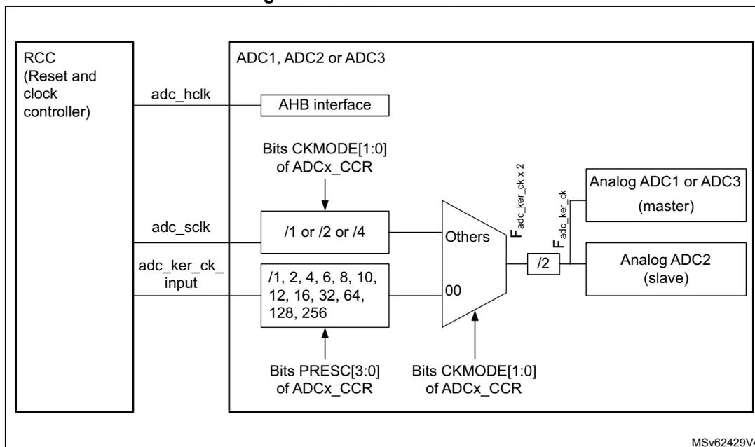
The diagram illustrates the ADC clock scheme. On the left, the RCC (Reset and clock controller) provides three clock signals: adc_hclk , adc_sclk , and adc_ker_ck_input . These signals enter a block labeled "ADC1, ADC2 or ADC3". Inside this block, the adc_hclk signal connects to an "AHB interface". The adc_sclk signal is divided by 1, 2, or 4 based on the "Bits CKMODE[1:0] of ADCx_CCR". The adc_ker_ck_input signal is divided by 1, 2, 4, 6, 8, 10, 12, 16, 32, 64, 128, or 256 based on the "Bits PRESC[3:0] of ADCx_CCR". Both divided signals enter a multiplexer labeled "Others" which is controlled by "Bits CKMODE[1:0] of ADCx_CCR". The output of the multiplexer is F adc_ker_ck × 2 . This signal is then divided by 2 to produce F adc_ker_ck , which is used by "Analog ADC1 or ADC3 (master)" and "Analog ADC2 (slave)".
MSV62429V4
- 1. Refer to the RCC section to see how adc_hclk and adc_ker_ck_input can be generated.
Clock ratio constraint between ADC clock and AHB clock
There are generally no constraints to be respected for the ratio between the ADC clock and the AHB clock except if some injected channels are programmed. In this case, it is mandatory to respect the following ratio:
- • \( F_{adc\_hclk} \geq F_{adc\_ker\_ck} / 4 \) if the resolution of all channels are 16-bit, 14-bit, 12-bit or 10-bit
- • \( F_{adc\_hclk} \geq F_{adc\_ker\_ck} / 3 \) if there are some channels with resolutions equal to 8-bit (and none with lower resolutions)
Constraints between ADC clocks
When several ADC interfaces are used simultaneously, it is mandatory to use the same clock source from the RCC block without prescaler ratio, for all ADC interfaces.
BOOST control
The ADC boost mode can be controlled through the BOOST bitfield in the ADC_CR register. This bitfield must be set according to the ADC clock setting. Refer to the ADC_CR register description.
26.4.4 ADC1/2/3 connectivity
ADC1 and ADC2 are tightly coupled and share some external channels as described in the following figures.
ADC3 is instantiated separately, but some inputs are shared with ADC1 and ADC2.
Figure 143. ADC1 connectivity
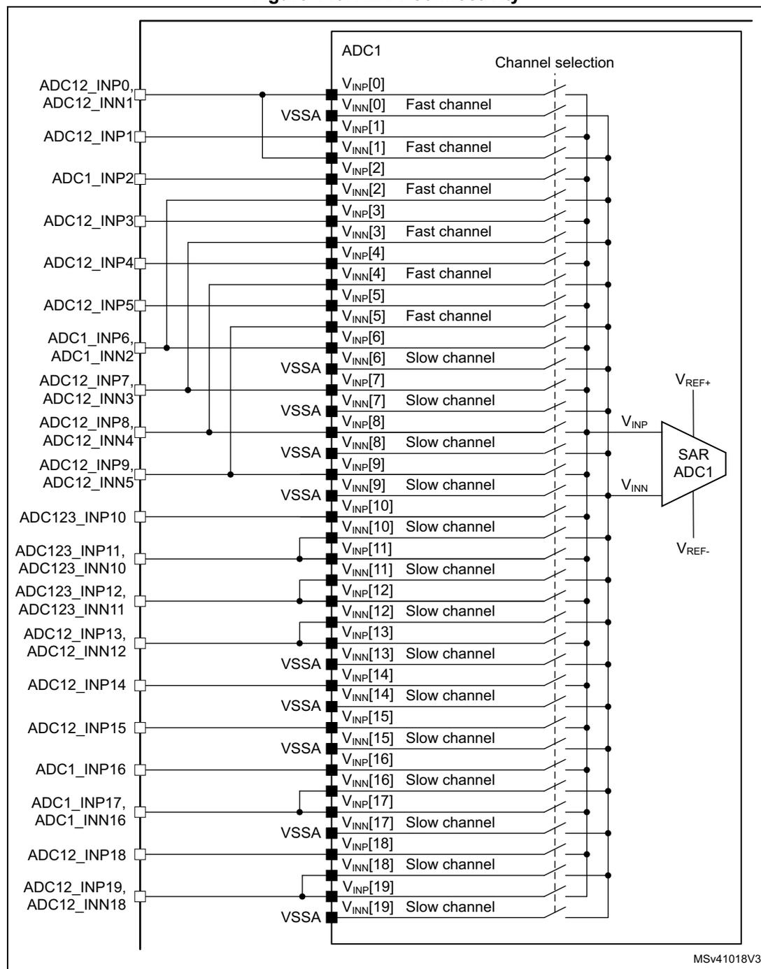
The diagram illustrates the internal connectivity of ADC1. It features 20 input channels, each consisting of a V INP and a V INN internal signal. The external pins on the left are labeled as follows:
- ADC12_INP0, ADC12_INN1
- ADC12_INP1
- ADC1_INP2
- ADC12_INP3
- ADC12_INP4
- ADC12_INP5
- ADC1_INP6, ADC1_INN2
- ADC12_INP7, ADC12_INN3
- ADC12_INP8, ADC12_INN4
- ADC12_INP9, ADC12_INN5
- ADC123_INP10
- ADC123_INP11, ADC123_INN10
- ADC123_INP12, ADC123_INN11
- ADC12_INP13, ADC12_INN12
- ADC12_INP14
- ADC12_INP15
- ADC1_INP16
- ADC1_INP17, ADC1_INN16
- ADC12_INP18
- ADC12_INP19, ADC12_INN18
Inside the ADC1 block, these pins map to internal signals V INP [0] through V INP [19] and V INN [0] through V INN [19]. Channels 0 to 5 are labeled "Fast channel", while channels 6 to 19 are labeled "Slow channel". Several V INN signals are tied to V SSA through internal switches. A "Channel selection" switch matrix connects the selected V INP and V INN signals to the SAR ADC1 core. The SAR ADC1 core also has connections for V REF+ and V REF- . The diagram is identified by the reference MSv41018V3.
- 1. ADCx_INNy signal can only be used when the corresponding ADC input channel is configured as differential mode.
Figure 144. ADC2 connectivity
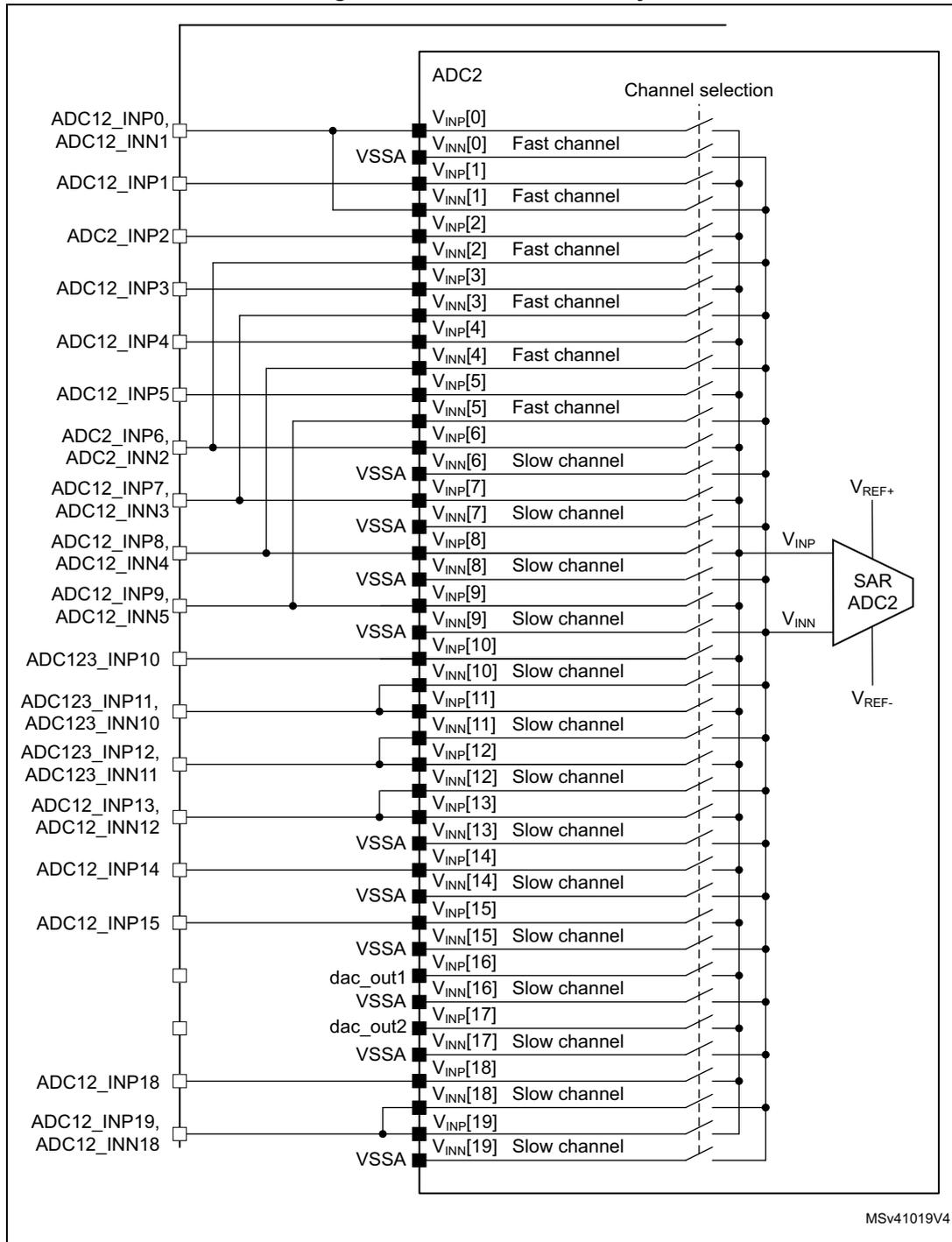
The diagram illustrates the internal connectivity of the ADC2 block. On the left, 20 differential input pairs are shown, labeled from ADC12_INP0/ADC12_INN1 to ADC12_INP19/ADC12_INN18. Each pair connects to an internal V_INP and V_INN pin pair. The V_INP pins are connected to the positive input (V_INP) of the SAR ADC2 block, and the V_INN pins are connected to the negative input (V_INN) of the SAR ADC2 block. The SAR ADC2 block also has V_REF+ and V_REF- pins. A 'Channel selection' block is shown on the right, with lines connecting it to each V_INP and V_INN pin pair. The V_INN pins are also connected to various internal signals: VSSA (for INP0, INP2, INP6, INP10, INP13, INP14, INP18), VSSA (for INP1, INP3, INP5, INP7, INP9, INP11, INP12, INP15, INP17, INP19), dac_out1 (for INP16), and dac_out2 (for INP18). The diagram also includes labels for 'Fast channel' and 'Slow channel' for each input pair.
MSv41019V4
- 1. ADCx_INNy signal can only be used when the corresponding ADC input channel is configured as differential mode.
Figure 145. ADC3 connectivity
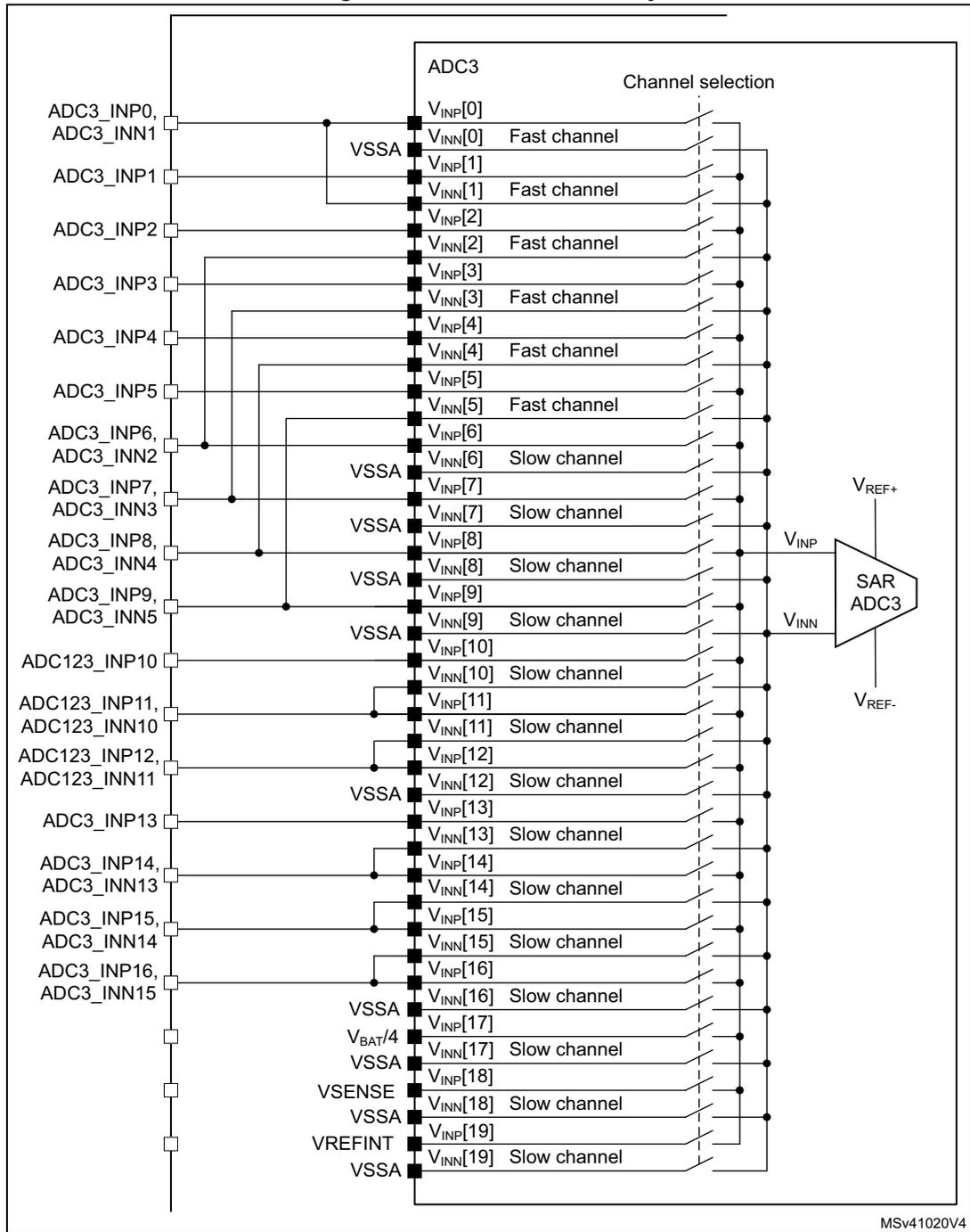
The diagram illustrates the internal connectivity of the ADC3 module. It features 20 differential input channels, each consisting of a positive input (V_INP[n]) and a negative input (V_INN[n]). Channels 0 through 5 are designated as 'Fast channel', while channels 6 through 19 are 'Slow channel'. The V_INP inputs are connected to external pins ADC3_INP0 through ADC3_INP16 and ADC123_INP10 through ADC123_INP12. The V_INN inputs are connected to internal VSSA rails or specific pins: V_INN[0] to VSSA, V_INN[1] to VSSA, V_INN[2] to VSSA, V_INN[3] to VSSA, V_INN[4] to VSSA, V_INN[5] to VSSA, V_INN[6] to VSSA, V_INN[7] to VSSA, V_INN[8] to VSSA, V_INN[9] to VSSA, V_INN[10] to VSSA, V_INN[11] to VSSA, V_INN[12] to VSSA, V_INN[13] to VSSA, V_INN[14] to VSSA, V_INN[15] to VSSA, V_INN[16] to VSSA, V_INN[17] to V_BAT/4, V_INN[18] to V_SENSE, and V_INN[19] to VREFINT. All V_INN inputs are also connected to a common VSSA rail. The SAR ADC3 block receives V_INP and V_INN signals and is referenced by V_REF+ and V_REF-.
- 1. ADCx_INNy signal can only be used when the corresponding ADC input channel is configured as differential mode.
26.4.5 Slave AHB interface
The ADCs implement an AHB slave port for control/status register and data access. The features of the AHB interface are listed below:
- • Word (32-bit) accesses
- • Single cycle response
- • Response to all read/write accesses to the registers with zero wait states.
The AHB slave interface does not support split/retry requests, and never generates AHB errors.
26.4.6 ADC deep-power-down mode (DEEPPWD) and ADC voltage regulator (ADVREGEN)
By default, the ADC is in deep-power-down mode where its supply is internally switched off to reduce the leakage currents (the reset state of bit DEEPPWD is 1 in the ADC_CR register).
To start ADC operations, it is first needed to exit deep-power-down mode by clearing bit DEEPPWD=0.
Then, it is mandatory to enable the ADC internal voltage regulator by setting the bit ADVREGEN=1 into ADC_CR register. The software must wait for the startup time of the ADC voltage regulator ( \( T_{ADCVREG\_STUP} \) ) before launching a calibration or enabling the ADC. This delay must be implemented by software.
The LDO status can be verified by checking the LDORDY bit in ADC_ISR register (refer to Section 26.3: ADC implementation for the availability of the LDO regulator status).
For the startup time of the ADC voltage regulator, refer to device datasheet for \( T_{ADCVREG\_STUP} \) parameter.
After ADC operations are complete, the ADC can be disabled (ADEN=0). It is possible to save power by also disabling the ADC voltage regulator. This is done by writing bit ADVREGEN=0.
Then, to save more power by reducing the leakage currents, it is also possible to re-enter in ADC deep-power-down mode by setting bit DEEPPWD=1 into ADC_CR register. This is particularly interesting before entering Stop mode.
Note: Writing DEEPPWD=1 automatically disables the ADC voltage regulator and bit ADVREGEN is automatically cleared.
Note: When the internal voltage regulator is disabled (ADVREGEN=0), the internal analog calibration is kept.
In ADC deep-power-down mode (DEEPPWD=1), the internal analog calibration is lost and it is necessary to either relaunch a calibration or apply again the calibration factor which was previously saved (refer to Section 26.4.8: Calibration (ADCAL, ADCALDIF, ADCALLIN, ADC_CALFACT) ).
26.4.7 Single-ended and differential input channels
Channels can be configured to be either single-ended input or differential input by writing into bits DIFSEL[19:0] in the ADC_DIFSEL register. This configuration must be written while the ADC is disabled (ADEN=0).
In single-ended input mode, the analog voltage to be converted for channel “i” is the difference between the external voltage \( V_{INP[i]} \) (positive input) and \( V_{REF-} \) (negative input).
In differential input mode, the analog voltage to be converted for channel “i” is the difference between the external voltage \( V_{INP[i]} \) (positive input) and \( V_{INN[i]} \) (negative input).
The output data for the differential mode is an unsigned data. When \( V_{INP[i]} \) equals \( V_{REF-} \) , \( V_{INN[i]} \) equals \( V_{REF+} \) and the output data is 0x0000 (16-bit resolution mode). When \( V_{INP[i]} \) equals \( V_{REF+} \) , \( V_{INN[i]} \) equals \( V_{REF-} \) and the output data is 0xFFFF.
When ADC is configured as differential mode, both input should be biased at \( V_{REF+} / 2 \) voltage.
The input signal are supposed to be differential (common mode voltage should be fixed).
For a complete description of how the input channels are connected for each ADC, refer to Section 26.4.4: ADC1/2/3 connectivity .
Caution: When configuring the channel “i” in differential input mode, its negative input voltage is connected to \( V_{INN[i]} \) . As a consequence, channel “i+n”, which is connected to \( V_{INN[i]} \) , should not be converted at same time by different ADCs. Some channels are shared between ADC1/ADC2: this can make the channel on the other ADC unusable.
26.4.8 Calibration (ADCAL, ADCALDIF, ADCALLIN, ADC_CALFACT)
Each ADC provides an automatic calibration procedure which drives all the calibration sequence including the power-on/off sequence of the ADC. During the procedure, the ADC calculates a calibration factor which is 11-bits of offset or 160-bits of linearity and which is applied internally to the ADC until the next ADC power-off. During the calibration procedure, the application must not use the ADC and must wait until calibration is complete.
The calibration is preliminary to any ADC operation. It removes the systematic errors which may vary from chip to chip and allows to compensate offset and linearity deviation.
The calibration factor for the offset to be applied for single-ended input conversions is different from the factor to be applied for differential input conversions:
- • Write ADCALDIF = 0 before launching a calibration which is applied for single-ended input conversions.
- • Write ADCALDIF = 1 before launching a calibration which is applied for differential input conversions.
The linearity correction must be done once only, regardless of single / differential configuration.
- • Write ADCALLIN = 1 before launching a calibration which runs the linearity calibration same time as the offset calibration.
- • Write ADCALLIN = 0 before launching a calibration which does not run the linearity calibration but only the offset calibration.
The calibration is then initiated by software by setting bit ADCCAL=1. It can be initiated only when the ADC is disabled (when ADEN=0). ADCCAL bit stays at 1 during all the calibration sequence. It is then cleared by hardware as soon the calibration completes. At this time, the associated calibration factor is stored internally in the analog ADC and also in the bits CALFACT_S[10:0] or CALFACT_D[10:0] of ADC_CALFACT register (depending on single-ended or differential input calibration). The 160-bit linearity calibration factor can be accessed using the ADC_CALFACT2 register with ADEN set to 1.
The internal analog calibration is kept if the ADC is disabled (ADEN=0). However, if the ADC is disabled for extended periods, it is recommended that a new offset calibration cycle is run before enabling again the ADC.
The internal analog calibration is lost each time the power of the ADC is removed (example, when the product enters in STANDBY or VBAT mode). In this case, to avoid spending time recalibrating the ADC, it is possible to re-write the calibration factor into the ADC_CALFACT and ADC_CALFACT2 register without recalibrating, supposing that the software has previously saved the calibration factor delivered during the previous calibration.
The calibration factor can be written if the ADC is enabled but not converting (ADEN=1 and ADSTART=0 and JADSTART=0). Then, at the next start of conversion, the calibration factor is automatically injected into the analog ADC. This loading is transparent and does not add any cycle latency to the start of the conversion. It is recommended to recalibrate when V REF+ voltage changed more than 10%.
Refer to the datasheets for the clock cycle requirement for both linear and offset calibration.
Software procedure to calibrate the ADC
- 1. Ensure DEEPPWD=0, ADVREGEN=1 and verify that the ADC voltage regulator startup time has elapsed by checking the LDORDY bit in ADC_ISR (refer to Section 26.3: ADC implementation for the availability of the LDO regulator status).
- 2. Ensure that ADEN=0.
- 3. Select the input mode for this calibration by setting ADCALDIF=0 (single-ended input) or ADCALDIF=1 (Differential input). Select if Linearity calibration enable or not by ADCALLIN=1(enabled) or ADCALLIN=0(disabled).
- 4. Set ADCCAL=1.
- 5. Wait until ADCCAL=0.
- 6. The offset calibration factor can be read from ADC_CALFACT register.
- 7. The linearity calibration factor can be read from ADC_CALFACT2 register, following the procedure described in Section : Linearity calibration reading procedure (ADEN must be set to 1 prior to accessing ADC_CALFACT2 register).
Figure 146. ADC calibration
![Timing diagram for ADC calibration showing signal transitions and states for ADCALDIF, ADCALLIN, ADCAL, ADC State, CALFACT_x[10:0], and LINCALFACT [159:0].](/RM0399-STM32H745-755-747-757/676f4c06f4867ce4f4a007652a4d6c6d_img.jpg)
The diagram illustrates the timing for ADC calibration. It shows the following signals and states:
- ADCALDIF : 0: Single-ended input, 1: Differential input. This signal is set by software (S/W).
- ADCALLIN : 0: Linear calibration disable, 1: Linear calibration enable. This signal is set by software (S/W).
- ADCAL : A signal that is set by hardware (H/W). A timing interval \( t_{CAB} \) is indicated between the rising edge of ADCAL and the transition of the ADC State.
- ADC State : Transitions from OFF to Startup, then to Calibrate, and finally back to OFF.
- CALFACT_x[10:0] : Initial value is 0x000. It is updated to a Calibration factor.
- LINCALFACT [159:0] : Initial value is 0x00000000000000000000. It is updated to a Calibration factor.
Legend: by S/W (software), by H/W (hardware), Indicative timings.
MSv41021V1
Software procedure to re-inject a calibration factor into the ADC
- 1. Ensure ADEN=1 and ADSTART=0 and JADSTART=0 (ADC enabled and no conversion is ongoing).
- 2. Write CALFACT_S and CALFACT_D with the new offset calibration factors.
- 3. Write LINCALFACT bits with the new linearity calibration factors, following the procedure described in Section : Linearity calibration writing procedure .
- 4. When a conversion is launched, the calibration factor is injected into the analog ADC only if the internal analog calibration factor differs from the one stored in bits CALFACT_S for single-ended input channel or bits CALFACT_D for differential input channel.
Figure 147. Updating the ADC offset calibration factor
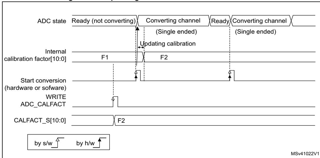
The diagram illustrates the timing for updating the ADC offset calibration factor. It shows the following signals and states:
- ADC state : Transitions from Ready (not converting) to Converting channel (Single ended), then back to Ready, and then to another Converting channel (Single ended).
- Internal calibration factor[10:0] : Transitions from F1 to F2 during the 'Updating calibration' phase, which occurs while the ADC is in the Converting channel state.
- Start conversion (hardware or software) : A signal that triggers the conversion. It is set by software (S/W).
- WRITE ADC_CALFACT : A signal that is set by software (S/W).
- CALFACT_S[10:0] : Transitions from F1 to F2.
Legend: by s/w (software), by h/w (hardware).
MSv41022V1
Calibrating single-ended and differential analog inputs with a single ADC
If the ADC is supposed to convert both differential and single-ended inputs, two calibrations must be performed, one with ADCALDIF=0 and one with ADCALDIF=1. The procedure is the following:
- 1. Disable the ADC.
- 2. Calibrate the ADC in single-ended input mode (with ADCALDIF=0) and Linearity calibration enable (with ADCALLIN=1). This updates the registers CALFACT_S[10:0] and LINCALFACT[159:0].
- 3. Calibrate the ADC in differential input modes (with ADCALDIF=1) and Linearity calibration disable (with ADCALLIN=0). This updates the register CALFACT_D[10:0].
- 4. Enable the ADC, configure the channels and launch the conversions. Each time there is a switch from a single-ended to a differential inputs channel (and vice-versa), the calibration is automatically injected into the analog ADC.
Figure 148. Mixing single-ended and differential channels
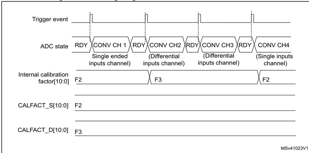
The diagram illustrates the timing of an ADC when mixing single-ended and differential channels. It consists of five horizontal timelines:
- Trigger event: Shows four rising edges that initiate the conversion sequence.
- ADC state: Shows the state of the ADC for each channel: RDY (Ready) followed by CONV (Conversion) for CH1, CH2, CH3, and CH4. CH1 is a single-ended input, CH2 and CH3 are differential inputs, and CH4 is a single-ended input.
- Internal calibration factor[10:0]: Shows the calibration factor used during each conversion: F2 for CH1, F3 for CH2, F3 for CH3, and F2 for CH4.
- CALFACT_S[10:0]: Shows the single-ended calibration factor, which is F2.
- CALFACT_D[10:0]: Shows the differential calibration factor, which is F3.
The diagram indicates that the internal calibration factor is automatically updated based on the type of input channel (single-ended or differential) when the ADC is configured to use both.
MSv41023V1
Linearity calibration reading procedure
Once the calibration is done (ADCAL bit cleared by hardware) with ADCALLIN=1, the 160-bit linearity correction factor can be read using the ADC_CALFACT2 30-bit registers (6 read accesses are necessary).
The six LINCALRDYW1..6 control/status bits in ADC_CR are set when the calibration is complete. When ADEN is set to 1, clearing one of these bits launches the transfer of part of the linearity factor into the LINCALFACT[29:0] of the ADC_CALFACT2 register. The bit is reset by hardware when the ADC_CALFACT2 register can be read (software must poll the bit until it is cleared). The complete procedure is as following:
- 1. Ensure DEEPPWD=0, ADVREGEN=1 and that the ADC voltage regulator startup time has elapsed by checking the LDORDY bit in ADC_ISR (refer to Section 26.3: ADC implementation for the availability of the LDO regulator status).
- 2. Set ADEN = 1 and wait until ADRDY=1.
- 3. Clear LINCALRDYW6 bit (Linearity calibration ready Word 6).
- 4. Poll LINCALRDYW6 bit until returned value is zero, indicating linearity correction bits[159:150] are available in ADC_CALFACT2[29:0].
- 5. Read ADC_CALFACT2[29:0].
- 6. Clear LINCALRDYW5 bit.
- 7. Poll LINCALRDYW5 bit until returned value is zero, indicating linearity correction bits[149:120] are available in ADC_CALFACT2[29:0].
- 8. Read ADC_CALFACT2[29:0].
- 9. Clear LINCALRDYW4 bit.
- 10. Poll LINCALRDYW4 bit until returned value is zero, indicating linearity correction bits[119:90] are available in ADC_CALFACT2[29:0].
- 11. Read ADC_CALFACT2[29:0].
- 12. Clear LINCALRDYW3 bit.
- 13. Poll LINCALRDYW3 bit until returned value is zero, indicating linearity correction bits[89:60] are available in ADC_CALFACT2[29:0].
- 14. Read ADC_CALFACT2[29:0].
- 15. Clear LINCALRDYW2 bit.
- 16. Poll LINCALRDYW2 bit until returned value is zero, indicating linearity correction bits[59:30] are available in ADC_CALFACT2[29:0].
- 17. Read ADC_CALFACT2[29:0].
- 18. Clear LINCALRDYW1 bit.
- 19. Poll LINCALRDYW1 bit until returned value is zero, indicating linearity correction bits[29:0] are available in ADC_CALFACT2[29:0].
- 20. Read ADC_CALFACT2[29:0].
Note: The software is allowed to toggle a single LINCALRDYWx bit at once (other bits left unchanged), otherwise causing unexpected behavior.
The software can access the linearity calibration factor by writing LINCALRDYW1..6 bits only when ADEN=1 and ADSTART=0 and JADSTART=0 (ADC enabled and no conversion is ongoing).
Linearity calibration writing procedure
The six LINCALRDYW1..6 control/status bits in ADC_CR are reset when the calibration has not yet been done or a new linearity calibration factor have been rewritten. It is possible to force directly a linearity calibration factor or re-inject it using the following procedure:
- 1. Ensure DEEPPWD=0, ADVREGEN=1 and that ADC voltage regulator startup time has elapsed by checking the LDORDY bit in ADC_ISR (refer to Section 26.3: ADC implementation for the availability of the LDO regulator status).
- 2. Set ADEN = 1 and wait until ADRDY=1.
- 3. Write ADC_CALFACT2[9:0] with previously saved linearity correction factor bits[159:150].
- 4. Set LINCALRDYW6 bit.
- 5. Poll LINCALRDYW6 bit until returned value is one, indicating linearity correction bits[159:150] have been effectively written.
- 6. Write ADC_CALFACT2[29:0] with previously saved linearity correction factor bits[149:120].
- 7. Set LINCALRDYW5 bit.
- 8. Poll LINCALRDYW5 bit until returned value is one, indicating linearity correction bits[149:120] have been effectively written.
- 9. Write ADC_CALFACT2[29:0] with previously saved linearity correction factor bits[119:90].
- 10. Set LINCALRDYW4 bit.
- 11. Poll LINCALRDYW4 bit until returned value is one, indicating linearity correction bits[119:90] have been effectively written.
- 12. Write ADC_CALFACT2[29:0] with previously saved linearity correction factor bits[89:60].
- 13. Set LINCALRDYW3 bit.
- 14. Poll LINCALRDYW3 bit until returned value is one, indicating linearity correction bits[89:60] have been effectively written.
- 15. Write ADC_CALFACT2[29:0] with previously saved linearity correction factor bits[59:30].
- 16. Set LINCALRDYW2 bit.
- 17. Poll LINCALRDYW2 bit until returned value is one, indicating linearity correction bits[59:30] have been effectively written.
- 18. Write ADC_CALFACT2[29:0] with previously saved linearity correction factor bits[29:0].
- 19. Set LINCALRDYW1 bit.
- 20. Poll LINCALRDYW1 bit until returned value is one, indicating linearity correction bits[29:0] have been effectively written.
Note: The software is allowed to toggle a single LINCALRDYWx bit at once (other bits left unchanged), otherwise causing unexpected behavior.
The software is allowed to update the linearity calibration factor by writing LINCALRDYW1..6 bits only when ADEN=1 and ADSTART=0 and JADSTART=0 (ADC enabled and no conversion is ongoing).
26.4.9 ADC on-off control (ADEN, ADDIS, ADRDY)
First of all, follow the procedure explained in Section 26.4.6: ADC deep-power-down mode (DEEPPWD) and ADC voltage regulator (ADVREGEN) .
Once DEEPPWD = 0 and ADVREGEN = 1, the ADC can be enabled and the ADC needs a stabilization time of \( t_{STAB} \) before it starts converting accurately, as shown in Figure 149 . Two control bits enable or disable the ADC:
- • ADEN = 1 enables the ADC. The flag ADRDY is set once the ADC is ready for operation.
- • ADDIS = 1 disables the ADC. ADEN and ADDIS are then automatically cleared by hardware as soon as the analog ADC is effectively disabled.
Regular conversion can then start either by setting ADSTART=1 (refer to Section 26.4.19: Conversion on external trigger and trigger polarity (EXTSEL, EXTEN, JEXTSEL, JEXTEN) ) or when an external trigger event occurs, if triggers are enabled.
Injected conversions start by setting JADSTART=1 or when an external injected trigger event occurs, if injected triggers are enabled.
Software procedure to enable the ADC
- 1. Clear the ADRDY bit in the ADC_ISR register by writing '1'.
- 2. Set ADEN=1.
- 3. Wait until ADRDY=1 (ADRDY is set after the ADC startup time). This can be done using the associated interrupt (setting ADRDYIE=1).
- 4. Clear the ADRDY bit in the ADC_ISR register by writing '1' (optional).
Software procedure to disable the ADC
- 1. Check that both ADSTART=0 and JADSTART=0 to ensure that no conversion is ongoing. If required, stop any regular and injected conversion ongoing by setting ADSTP=1 and JADSTP=1 and then wait until ADSTP=0 and JADSTP=0.
- 2. Set ADDIS=1.
- 3. If required by the application, wait until ADEN=0, until the analog ADC is effectively disabled (ADDIS is automatically reset once ADEN=0).
Figure 149. Enabling / Disabling the ADC
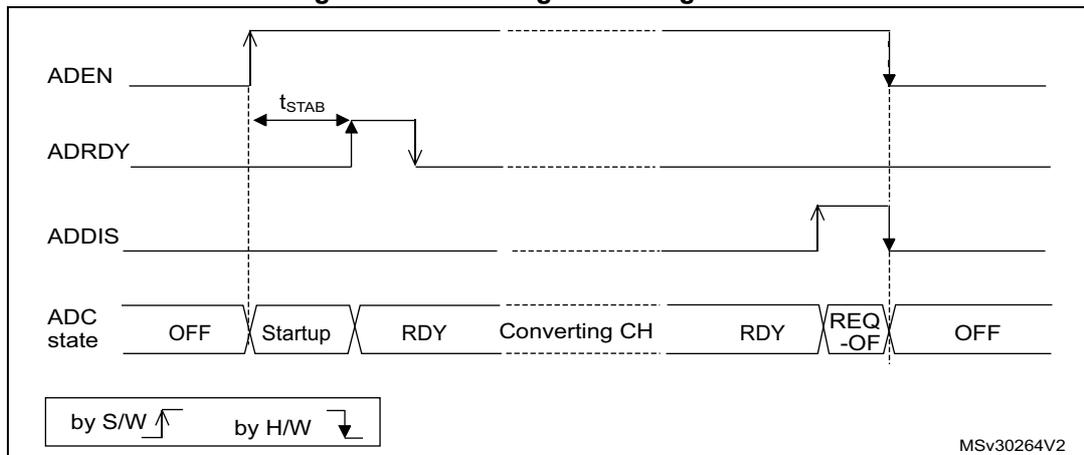
MSV30264V2
26.4.10 Constraints when writing the ADC control bits
The software can write the RCC control bits to configure and enable the ADC clock (refer to RCC Section), the control bits DIFSEL in the ADC_DIFSEL register, ADCx_CCR register and the control bits ADCAL and ADEN in the ADC_CR register, only if the ADC is disabled (ADEN must be equal to 0).
The software is then allowed to write the control bits ADSTART, JADSTART and ADDIS of the ADC_CR register only if the ADC is enabled and there is no pending request to disable the ADC (ADEN must be equal to 1 and ADDIS to 0).
For all the other control bits of the ADC_CFGR, ADC_SMPRy, ADC_TRy, ADC_SQry, ADC_JDRy, ADC_OFRy and ADC_IER registers:
- • For control bits related to configuration of regular conversions, the software is allowed to write them only if there is no regular conversion ongoing (ADSTART must be equal to 0).
- • For control bits related to configuration of injected conversions, the software is allowed to write them only if there is no injected conversion ongoing (JADSTART must be equal to 0).
The software can write ADSTP or JADSTP control bits in the ADC_CR register only if the ADC is enabled and eventually converting and if there is no pending request to disable the ADC (ADSTART or JADSTART must be equal to 1 and ADDIS to 0).
The software can write the register ADC_JSQR at any time, when the ADC is enabled (ADEN=1).
The software is allowed to write the ADC_JSQR register only when JADSTART is cleared to 0 (no injected conversion is ongoing) unless the context queue is enabled (JQDIS=0 in ADC_CFGR register).
Note: There is no hardware protection to prevent these forbidden write accesses and ADC behavior may become in an unknown state. To recover from this situation, the ADC must be disabled (clear ADEN=0 as well as all the bits of ADC_CR register).
26.4.11 Channel selection (SQRx, JSQRx)
There are up to 20 multiplexed channels per ADC:
- • 6 fast analog inputs coming from Analog PADs and GPIO pads (ADCx_INP/INN[0..5])
- • Up to 14 slow analog inputs coming from GPIO pads (ADCx_INP/INN[6..19]).
- • The ADCs are connected to 5 internal analog inputs:
- – the internal temperature sensor ( \( V_{\text{SENSE}} \) )
- – the internal reference voltage ( \( V_{\text{REFINT}} \) )
- – the \( V_{\text{BAT}} \) monitoring channel ( \( V_{\text{BAT}}/4 \) )
- – DAC internal channels
Refer to Table ADC interconnection in Section 26.4.2: ADC pins and internal signals for the connection of the above internal analog inputs to external ADC pins or internal signals.
It is possible to organize the conversions in two groups: regular and injected. A group consists of a sequence of conversions that can be done on any channel and in any order. For instance, it is possible to implement the conversion sequence in the following order:
ADCx_INP/INN3, ADCx_INP/INN8, ADCx_INP/INN2, ADCx_INP/INN2, ADCx_INP/INN0, ADCx_INP/INN2, ADCx_INP/INN2, ADCx_INP/INN15.
- • A regular group is composed of up to 16 conversions. The regular channels and their order in the conversion sequence must be selected in the ADC_SQRy registers. The total number of conversions in the regular group must be written in the L[3:0] bits in the ADC_SQR1 register.
- • An injected group is composed of up to 4 conversions. The injected channels and their order in the conversion sequence must be selected in the ADC_JSQR register. The total number of conversions in the injected group must be written in the L[1:0] bits in the ADC_JSQR register.
ADC_SQRy registers must not be modified while regular conversions can occur. For this, the ADC regular conversions must be first stopped by writing ADSTP=1 (refer to Section 26.4.18: Stopping an ongoing conversion (ADSTP, JADSTP) ).
The software is allowed to modify on-the-fly the ADC_JSQR register when JADSTART is set to 1 only when the context queue is enabled (JQDIS=0 in ADC_CFGR register).
Temperature sensor, V REFINT and V BAT internal channels
The internal reference voltage (V REFINT ), the temperature sensor (V SENSE ), and the V BAT channel are connected to ADC internal channels. Refer to Table ADC interconnection in Section 26.4.2: ADC pins and internal signals for details.
Note: To convert one of the internal analog channels, enable the corresponding analog sources by programming VREFEN, TSEN and VBATEN bits in the ADCx_CCR registers.
26.4.12 Channel preselection register (ADC_PCSEL)
For each channel selected through SQRx or JSQRx, the corresponding ADC_PCSEL bit must be previously configured.
This ADC_PCSEL bit controls the analog switch integrated in the I/O level. The ADC input MUX selects the ADC input according to the SQRx and JSQRx with very high speed, the analog switch integrated in the IO cannot react as fast as ADC mux does. To avoid the delay on analog switch control on IO, it is necessary to preselect the input channels which are selected in the SQRx, JSQRx.
The selection is based on the V INP[ij] of each ADC input. If ADC1 converts the ADC123_INP2(V INP[2] ) as differential mode, ADC123_INP6(V INP[6] ) also needs to be selected in ADC_PCSEL.
Some I/Os are connected to several V INP[ij] of the ADCx. The control inputs of the analog switch are ORed with the corresponding ADC_PCSEL register bits.
26.4.13 Channel-wise programmable sampling time (SMPR1, SMPR2)
Before starting a conversion, the ADC must establish a direct connection between the voltage source under measurement and the embedded sampling capacitor of the ADC. This sampling time must be enough for the input voltage source to charge the embedded capacitor to the input voltage level.
Each channel can be sampled with a different sampling time which is programmable using the SMP[2:0] bits in the ADC_SMPR1 and ADC_SMPR2 registers. It is therefore possible to select among the following sampling time values:
- • SMP = 000: 1.5 ADC clock cycles
- • SMP = 001: 2.5 ADC clock cycles
- • SMP = 010: 8.5 ADC clock cycles
- • SMP = 011: 16.5 ADC clock cycles
- • SMP = 100: 32.5 ADC clock cycles
- • SMP = 101: 64.5 ADC clock cycles
- • SMP = 110: 387.5 ADC clock cycles
- • SMP = 111: 810.5 ADC clock cycles
The total conversion time is calculated as follows:
Example:
With \( F_{\text{adc\_ker\_ck}} = 24 \text{ MHz} \) and a sampling time of 1.5 ADC clock cycles (14-bit mode):
The ADC notifies the end of the sampling phase by setting the status bit EOSMP (only for regular conversion).
Constraints on the sampling time for fast and slow channels
For each channel, SMP[2:0] bits must be programmed to respect a minimum sampling time as specified in the ADC characteristics section of the datasheets.
I/O analog switch voltage booster
The resistance of the I/O analog switches increases when the \( V_{\text{DDA}} \) voltage is too low. The sampling time must consequently be adapted accordingly (refer to the device datasheet for the corresponding electrical characteristics). This resistance can be minimized at low \( V_{\text{DDA}} \) voltage by enabling an internal voltage booster through the BOOSTE bit of the SYSCFG_PMCR register.
26.4.14 Single conversion mode (CONT=0)
In single conversion mode, the ADC performs once all the conversions of the channels. This mode is started with the CONT bit at 0 by either:
- • Setting the ADSTART bit in the ADC_CR register (for a regular channel, with software trigger selected)
- • Setting the JADSTART bit in the ADC_CR register (for an injected channel, with software trigger selected)
- • External hardware trigger event (for a regular or injected channel)
- ADSTART bit or JADSTART bit must be set before triggering an external event.
Inside the regular sequence, after each conversion is complete:
- • The converted data are stored into the 32-bit ADC_DR register
- • The EOC (end of regular conversion) flag is set
- • An interrupt is generated if the EOCIE bit is set
Inside the injected sequence, after each conversion is complete:
- • The converted data are stored into one of the four 32-bit ADC_JDRy registers
- • The JEOC (end of injected conversion) flag is set
- • An interrupt is generated if the JEOCIE bit is set
After the regular sequence is complete:
- • The EOS (end of regular sequence) flag is set
- • An interrupt is generated if the EOSIE bit is set
After the injected sequence is complete:
- • The JEOS (end of injected sequence) flag is set
- • An interrupt is generated if the JEOSIE bit is set
Then the ADC stops until a new external regular or injected trigger occurs or until bit ADSTART or JADSTART is set again.
Note: To convert a single channel, program a sequence with a length of 1.
26.4.15 Continuous conversion mode (CONT=1)
This mode applies to regular channels only.
In continuous conversion mode, when a software or hardware regular trigger event occurs, the ADC performs once all the regular conversions of the channels and then automatically re-starts and continuously converts each conversions of the sequence. This mode is started with the CONT bit at 1 either by external trigger or by setting the ADSTART bit in the ADC_CR register.
Inside the regular sequence, after each conversion is complete:
- • The converted data are stored into the 32-bit ADC_DR register
- • The EOC (end of conversion) flag is set
- • An interrupt is generated if the EOCIE bit is set
After the sequence of conversions is complete:
- • The EOS (end of sequence) flag is set
- • An interrupt is generated if the EOSIE bit is set
Then, a new sequence restarts immediately and the ADC continuously repeats the conversion sequence.
Note: To convert a single channel, program a sequence with a length of 1.
It is not possible to have both discontinuous mode and continuous mode enabled: it is forbidden to set both DISCEN=1 and CONT=1.
Injected channels cannot be converted continuously. The only exception is when an injected channel is configured to be converted automatically after regular channels in continuous mode (using JAUTO bit), refer to Auto-injection mode section ).
26.4.16 Starting conversions (ADSTART, JADSTART)
Software starts ADC regular conversions by setting ADSTART=1.
When ADSTART is set, the conversion starts:
- • Immediately: if EXTEN = 0x0 (software trigger)
- • At the next active edge of the selected regular hardware trigger: if EXTEN != 0x0
Software starts ADC injected conversions by setting JADSTART=1.
When JADSTART is set, the conversion starts:
- • Immediately, if JEXTEN = 0x0 (software trigger)
- • At the next active edge of the selected injected hardware trigger: if JEXTEN != 0x0
Note: In auto-injection mode (JAUTO=1), use ADSTART bit to start the regular conversions followed by the auto-injected conversions (JADSTART must be kept cleared).
ADSTART and JADSTART also provide information on whether any ADC operation is currently ongoing. It is possible to re-configure the ADC while ADSTART=0 and JADSTART=0 are both true, indicating that the ADC is idle.
ADSTART is cleared by hardware:
- • In single mode with software trigger (CONT=0, EXTEN=0x0)
- – at any end of conversion sequence (EOS =1)
- • In discontinuous mode with software trigger (CONT=0, DISCEN=1, EXTEN=0x0)
- – at end of conversion (EOC=1)
- • In all other cases (CONT=x, EXTEN=x)
- – after execution of the ADSTP procedure asserted by the software.
Note: In continuous mode (CONT=1), ADSTART is not cleared by hardware with the assertion of EOS because the sequence is automatically relaunched.
When a hardware trigger is selected in single mode (CONT=0 and EXTEN !=0x00), ADSTART is not cleared by hardware with the assertion of EOS to help the software which does not need to reset ADSTART again for the next hardware trigger event. This ensures that no further hardware triggers are missed.
JADSTART is cleared by hardware:
- • in single mode with software injected trigger (JEXTEN=0x0)
- – at any end of injected conversion sequence (JEOS assertion) or at any end of sub-group processing if JDISCEN=1
- • in all cases (JEXTEN=x)
- – after execution of the JADSTP procedure asserted by the software.
Note: When the software trigger is selected, ADSTART bit should not be set if the EOC flag is still high.
26.4.17 Timing
The elapsed time between the start of a conversion and the end of conversion is the sum of the configured sampling time plus the successive approximation time depending on data resolution:
Figure 150. Analog to digital conversion time
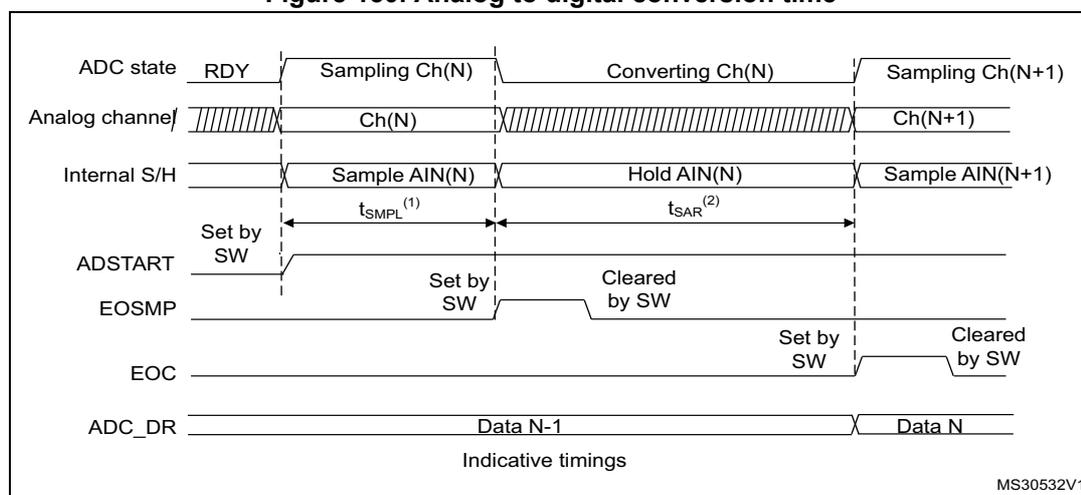
The diagram shows the timing of an ADC conversion. The top row shows the ADC state: RDY, Sampling Ch(N), Converting Ch(N), and Sampling Ch(N+1). The second row shows the analog channel: Ch(N) and Ch(N+1). The third row shows the internal S/H: Sample AIN(N), Hold AIN(N), and Sample AIN(N+1). The fourth row shows the ADSTART signal: Set by SW. The fifth row shows the EOSMP signal: Set by SW, Cleared by SW. The sixth row shows the EOC signal: Set by SW, Cleared by SW. The bottom row shows the ADC_DR register: Data N-1 and Data N. The diagram is labeled 'Indicative timings' and 'MS30532V1'.
1. \( T_{\text{SMPL}} \) depends on SMP[2:0]
2. \( T_{\text{SAR}} \) depends on RES[2:0]
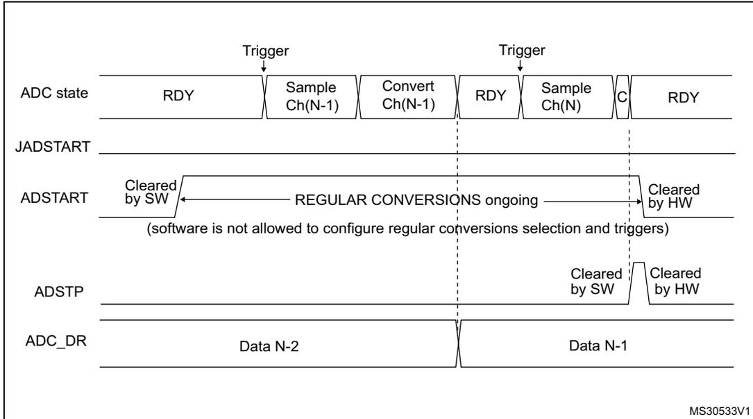
26.4.18 Stopping an ongoing conversion (ADSTP, JADSTP)
The software can decide to stop regular conversions ongoing by setting ADSTP=1 and injected conversions ongoing by setting JADSTP=1.
Stopping conversions resets the ongoing ADC operation. Then the ADC can be reconfigured (ex: changing the channel selection or the trigger) ready for a new operation.
Note that it is possible to stop injected conversions while regular conversions are still operating and vice-versa. This allows, for instance, re-configuration of the injected conversion sequence and triggers while regular conversions are still operating (and vice-versa).
When the ADSTP bit is set by software, any ongoing regular conversion is aborted with partial result discarded (ADC_DR register is not updated with the current conversion).
When the JADSTP bit is set by software, any ongoing injected conversion is aborted with partial result discarded (ADC_JDRy register is not updated with the current conversion). The scan sequence is also aborted and reset (meaning that relaunching the ADC would restart a new sequence).
Once this procedure is complete, bits ADSTP/ADSTART (in case of regular conversion), or JADSTP/JADSTART (in case of injected conversion) are cleared by hardware and the software must poll ADSTART (or JADSTART) until the bit is reset before assuming the ADC is completely stopped.
Note: In auto-injection mode (JAUTO=1), setting ADSTP bit aborts both regular and injected conversions (JADSTP must not be used).
Figure 151. Stopping ongoing regular conversions
The diagram illustrates the sequence of events for stopping ongoing regular conversions. The ADC state starts in RDY, then a 'Trigger' initiates 'Sample Ch(N-1)' and 'Convert Ch(N-1)'. After conversion, it returns to RDY. Another 'Trigger' initiates 'Sample Ch(N)' and 'Convert Ch(N)'. The ADSTART bit is set by software (SW) and cleared by hardware (HW) when conversions are ongoing. The ADSTP bit is set by software (SW) and cleared by hardware (HW). The ADC_DR register contains Data N-2 and Data N-1. A note indicates that software is not allowed to configure regular conversions selection and triggers.
Figure 152. Stopping ongoing regular and injected conversions
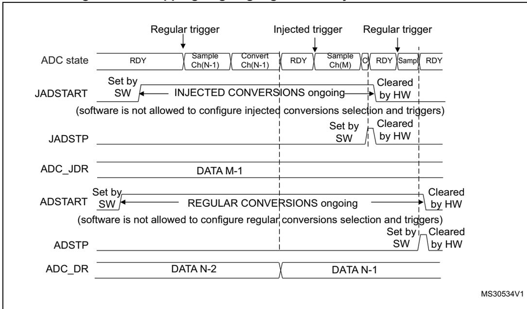
The diagram illustrates the sequence of events for stopping ongoing regular and injected conversions. The ADC state starts in RDY, then a 'Regular trigger' initiates 'Sample Ch(N-1)' and 'Convert Ch(N-1)'. After conversion, it returns to RDY. Then an 'Injected trigger' initiates 'Sample Ch(M)' and 'Convert Ch(M)'. After conversion, it returns to RDY. Then another 'Regular trigger' initiates 'Sample' and 'Convert'. The JADSTART bit is set by software (SW) and cleared by hardware (HW) when injected conversions are ongoing. The JADSTP bit is set by software (SW) and cleared by hardware (HW). The ADSTART bit is set by software (SW) and cleared by hardware (HW) when regular conversions are ongoing. The ADSTP bit is set by software (SW) and cleared by hardware (HW). The ADC_JDR register contains DATA M-1. The ADC_DR register contains DATA N-2 and DATA N-1. Notes indicate that software is not allowed to configure injected conversions selection and triggers, and regular conversions selection and triggers.
26.4.19 Conversion on external trigger and trigger polarity (EXTSEL, EXTEN, JEXTSEL, JEXTEN)
A conversion or a sequence of conversions can be triggered either by software or by an external event (e.g. timer capture, input pins). If the EXTEN[1:0] control bits (for a regular conversion) or JEXTEN[1:0] bits (for an injected conversion) are different from 0b00, then external events are able to trigger a conversion with the selected polarity.
When the Injected Queue is enabled (bit JQDIS=0), injected software triggers are not possible.
The regular trigger selection is effective once software has set bit ADSTART=1 and the injected trigger selection is effective once software has set bit JADSTART=1.
Any hardware triggers which occur while a conversion is ongoing are ignored.
- • If bit ADSTART=0, any regular hardware triggers which occur are ignored.
- • If bit JADSTART=0, any injected hardware triggers which occur are ignored.
Table 212 provides the correspondence between the EXTEN[1:0] and JEXTEN[1:0] values and the trigger polarity.
Table 212. Configuring the trigger polarity for regular external triggers
| EXTEN[1:0] | Source |
|---|---|
| 00 | Hardware Trigger detection disabled, software trigger detection enabled |
| 01 | Hardware Trigger with detection on the rising edge |
| 10 | Hardware Trigger with detection on the falling edge |
| 11 | Hardware Trigger with detection on both the rising and falling edges |
Note: The polarity of the regular trigger cannot be changed on-the-fly.
Table 213. Configuring the trigger polarity for injected external triggers
| JEXTEN[1:0] | Source |
|---|---|
| 00 |
|
| 01 | Hardware Trigger with detection on the rising edge |
| 10 | Hardware Trigger with detection on the falling edge |
| 11 | Hardware Trigger with detection on both the rising and falling edges |
Note: The polarity of the injected trigger can be anticipated and changed on-the-fly when the queue is enabled (JQDIS=0). Refer to Section 26.4.22: Queue of context for injected conversions .
The EXTSEL[4:0] and JEXTSEL[4:0] control bits select which out of 21 possible events can trigger conversion for the regular and injected groups.
A regular group conversion can be interrupted by an injected trigger.
Note:
The regular trigger selection cannot be changed on-the-fly.
The injected trigger selection can be anticipated and changed on-the-fly. Refer to
Section 26.4.22: Queue of context for injected conversions on page 983
Each ADC master shares the same input triggers with its ADC slave as described in Figure 153 .
Figure 153. Triggers are shared between ADC master and ADC slave
![Diagram showing trigger sharing between ADC MASTER and ADC SLAVE. The diagram illustrates how external triggers (adc_ext0_trg to adc_ext31_trg) and injected triggers (adc_jext0_trg to adc_jext31_trg) are connected to multiplexers within the ADC MASTER and ADC SLAVE blocks. The ADC MASTER has two multiplexers: one for 'External regular trigger' (EXTSEL[4:0]) and one for 'External injected trigger' (JEXTSEL[4:0]). The ADC SLAVE also has two multiplexers: one for 'External regular trigger' (EXTSEL[4:0]) and one for 'External injected trigger' (JEXTSEL[4:0]). The triggers are shared between the master and slave, with the master's triggers being connected to the slave's multiplexers as well. The diagram is labeled MSv41035V2.](/RM0399-STM32H745-755-747-757/ee963e19a2d944e48e795c8e0a2d76b3_img.jpg)
Table 214 and Table 215 give all the possible external triggers of the three ADCs for regular and injected conversion.
Table 214. ADC1, ADC2 and ADC3 - External triggers for regular channels
| Name | Source | Type | EXTSEL[4:0] |
|---|---|---|---|
| adc_ext_trg0 | tim1_oc1 | Internal signal from on-chip timers | 00000 |
| adc_ext_trg1 | tim1_oc2 | Internal signal from on-chip timers | 00001 |
| adc_ext_trg2 | tim1_oc3 | Internal signal from on-chip timers | 00010 |
| adc_ext_trg3 | tim2_oc2 | Internal signal from on-chip timers | 00011 |
| adc_ext_trg4 | tim3_trgo | Internal signal from on-chip timers | 00100 |
| adc_ext_trg5 | tim4_oc4 | Internal signal from on-chip timers | 00101 |
| adc_ext_trg6 | exti11 | External pin | 00110 |
| adc_ext_trg7 | tim8_trgo | Internal signal from on-chip timers | 00111 |
| adc_ext_trg8 | tim8_trgo2 | Internal signal from on-chip timers | 01000 |
| adc_ext_trg9 | tim1_trgo | Internal signal from on-chip timers | 01001 |
| Name | Source | Type | EXTSEL[4:0] |
|---|---|---|---|
| adc_ext_trg10 | tim1_trgo2 | Internal signal from on-chip timers | 01010 |
| adc_ext_trg11 | tim2_trgo | Internal signal from on-chip timers | 01011 |
| adc_ext_trg12 | tim4_trgo | Internal signal from on-chip timers | 01100 |
| adc_ext_trg13 | tim6_trgo | Internal signal from on-chip timers | 01101 |
| adc_ext_trg14 | tim15_trgo | Internal signal from on-chip timers | 01110 |
| adc_ext_trg15 | tim3_oc4 | Internal signal from on-chip timers | 01111 |
| adc_ext_trg16 | hrtim1_adctrig1 | Internal signal from on-chip timers | 10000 |
| adc_ext_trg17 | hrtim1_adctrig3 | Internal signal from on-chip timers | 10001 |
| adc_ext_trg18 | lptim1_out | Internal signal from on-chip timers | 10010 |
| adc_ext_trg19 | lptim2_out | Internal signal from on-chip timers | 10011 |
| adc_ext_trg20 | lptim3_out | Internal signal from on-chip timers | 10100 |
| adc_ext_trg21 | Reserved | - | 10101 |
| adc_ext_trg22 | Reserved | - | 10110 |
| adc_ext_trg23 | Reserved | - | 10111 |
| adc_ext_trg24 | Reserved | - | 11000 |
| adc_ext_trg25 | Reserved | - | 11001 |
| adc_ext_trg26 | Reserved | - | 11010 |
| adc_ext_trg27 | Reserved | - | 11011 |
| adc_ext_trg28 | Reserved | - | 11100 |
| adc_ext_trg29 | Reserved | - | 11101 |
| adc_ext_trg30 | Reserved | - | 11110 |
| adc_ext_trg31 | Reserved | - | 11111 |
| Name | Source | Type | JEXTSEL[4:0] |
|---|---|---|---|
| adc_jext_trg0 | tim1_trgo | Internal signal from on-chip timers | 00000 |
| adc_jext_trg1 | tim1_oc4 | Internal signal from on-chip timers | 00001 |
| adc_jext_trg2 | tim2_trgo | Internal signal from on-chip timers | 00010 |
| adc_jext_trg3 | tim2_oc1 | Internal signal from on-chip timers | 00011 |
| adc_jext_trg4 | tim3_oc4 | Internal signal from on-chip timers | 00100 |
| adc_jext_trg5 | tim4_trgo | Internal signal from on-chip timers | 00101 |
| adc_jext_trg6 | exti15 | External pin | 00110 |
| adc_jext_trg7 | tim8_oc4 | Internal signal from on-chip timers | 00111 |
| adc_jext_trg8 | tim1_trgo2 | Internal signal from on-chip timers | 01000 |
| adc_jext_trg9 | tim8_trgo | Internal signal from on-chip timers | 01001 |
| Name | Source | Type | JEXTSEL[4:0] |
|---|---|---|---|
| adc_jext_trg10 | tim8_trgo2 | Internal signal from on-chip timers | 01010 |
| adc_jext_trg11 | tim3_oc3 | Internal signal from on-chip timers | 01011 |
| adc_jext_trg12 | tim3_trgo | Internal signal from on-chip timers | 01100 |
| adc_jext_trg13 | tim3_oc1 | Internal signal from on-chip timers | 01101 |
| adc_jext_trg14 | tim6_trgo | Internal signal from on-chip timers | 01110 |
| adc_jext_trg15 | tim15_trgo | Internal signal from on-chip timers | 01111 |
| adc_jext_trg16 | hrtim1_adctrig2 | Internal signal from on-chip timers | 10000 |
| adc_jext_trg17 | hrtim1_adctrig4 | Internal signal from on-chip timers | 10001 |
| adc_jext_trg18 | lptim1_out | Internal signal from on-chip timers | 10010 |
| adc_jext_trg19 | lptim2_out | Internal signal from on-chip timers | 10011 |
| adc_jext_trg20 | lptim3_out | Internal signal from on-chip timers | 10100 |
| adc_jext_trg21 | Reserved | - | 10101 |
| adc_jext_trg22 | Reserved | - | 10110 |
| adc_jext_trg23 | Reserved | - | 10111 |
| adc_jext_trg24 | Reserved | - | 11000 |
| adc_jext_trg25 | Reserved | - | 11001 |
| adc_jext_trg26 | Reserved | - | 11010 |
| adc_jext_trg27 | Reserved | - | 11011 |
| adc_jext_trg28 | Reserved | - | 11100 |
| adc_jext_trg29 | Reserved | - | 11101 |
| adc_jext_trg30 | Reserved | - | 11110 |
| adc_jext_trg31 | Reserved | - | 11111 |
26.4.20 Injected channel management
Triggered injection mode
To use triggered injection, the JAUTO bit in the ADC_CFGR register must be cleared.
- 1. Start the conversion of a group of regular channels either by an external trigger or by setting the ADSTART bit in the ADC_CR register.
- 2. If an external injected trigger occurs, or if the JADSTART bit in the ADC_CR register is set during the conversion of a regular group of channels, the current conversion is reset and the injected channel sequence switches are launched (all the injected channels are converted once).
- 3. Then, the regular conversion of the regular group of channels is resumed from the last interrupted regular conversion.
- 4. If a regular event occurs during an injected conversion, the injected conversion is not interrupted but the regular sequence is executed at the end of the injected sequence. Figure 154 shows the corresponding timing diagram.
Note: When using triggered injection, one must ensure that the interval between trigger events is longer than the injection sequence. For instance, if the sequence length is 20 ADC clock cycles (that is two conversions with a sampling time of 1.5 clock periods), the minimum interval between triggers must be 21 ADC clock cycles.
Auto-injection mode
If the JAUTO bit in the ADC_CFGR register is set, then the channels in the injected group are automatically converted after the regular group of channels. This can be used to convert a sequence of up to 20 conversions programmed in the ADC_SQRy and ADC_JSQR registers.
In this mode, the ADSTART bit in the ADC_CR register must be set to start regular conversions, followed by injected conversions (JADSTART must be kept cleared). Setting the ADSTP bit aborts both regular and injected conversions (JADSTP bit must not be used).
In this mode, external trigger on injected channels must be disabled.
If the CONT bit is also set in addition to the JAUTO bit, regular channels followed by injected channels are continuously converted.
Note: It is not possible to use both the auto-injected and discontinuous modes simultaneously. When the DMA is used for exporting regular sequencer's data in JAUTO mode, it is necessary to program it in circular mode (CIRC bit set in DMA_CCRx register). If the CIRC bit is reset (single-shot mode), the JAUTO sequence is stopped upon DMA Transfer Complete event.
Figure 154. Injected conversion latency
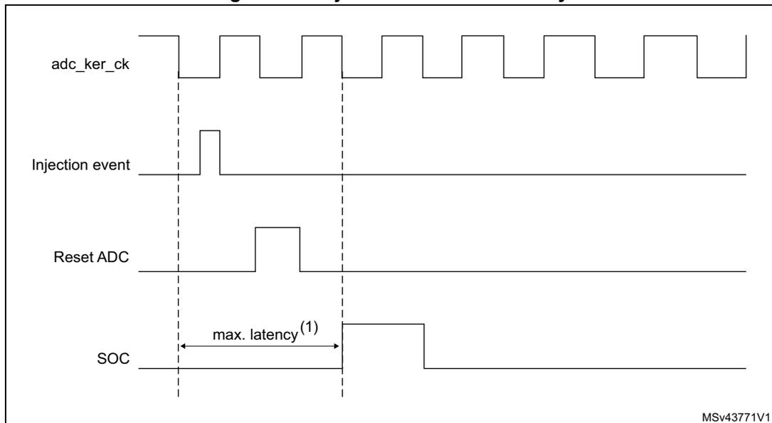
The timing diagram shows four signals over time. The top signal, 'adc_ker_ck', is a periodic square wave representing the ADC kernel clock. The second signal, 'Injection event', is a pulse that goes high and then low. The third signal, 'Reset ADC', is a pulse that goes high after the injection event and then low. The bottom signal, 'SOC' (Start of Conversion), is a pulse that goes high after the 'Reset ADC' signal goes low. A horizontal double-headed arrow labeled 'max. latency (1)' indicates the time interval between the rising edge of the 'Injection event' and the rising edge of the 'SOC' signal. Vertical dashed lines mark the key timing points: the rising edge of the injection event, the falling edge of the reset signal, and the rising edge of the SOC signal. The diagram is labeled 'MSV43771V1' in the bottom right corner.
- 1. The maximum latency value can be found in the electrical characteristics of the device datasheet.
26.4.21 Discontinuous mode (DISCEN, DISCNUM, JDISCEN)
Regular group mode
This mode is enabled by setting the DISCEN bit in the ADC_CFGR register.
It is used to convert a short sequence (sub-group) of n conversions ( \( n \leq 8 \) ) that is part of the sequence of conversions selected in the ADC_SQRy registers. The value of n is specified by writing to the DISCNUM[2:0] bits in the ADC_CFGR register.
When an external trigger occurs, it starts the next n conversions selected in the ADC_SQR registers until all the conversions in the sequence are done. The total sequence length is defined by the L[3:0] bits in the ADC_SQR1 register.
Example:
- • DISCEN=1, n=3, channels to be converted = 1, 2, 3, 6, 7, 8, 9, 10, 11
- – 1st trigger: channels converted are 1, 2, 3 (an EOC event is generated at each conversion).
- – 2nd trigger: channels converted are 6, 7, 8 (an EOC event is generated at each conversion).
- – 3rd trigger: channels converted are 9, 10, 11 (an EOC event is generated at each conversion) and an EOS event is generated after the conversion of channel 11.
- – 4th trigger: channels converted are 1, 2, 3 (an EOC event is generated at each conversion).
- – ...
- • DISCEN=0, channels to be converted = 1, 2, 3, 6, 7, 8, 9, 10, 11
- – 1st trigger: the complete sequence is converted: channel 1, then 2, 3, 6, 7, 8, 9, 10 and 11. Each conversion generates an EOC event and the last one also generates an EOS event.
- – all the next trigger events relaunch the complete sequence.
Note: When a regular group is converted in discontinuous mode, no rollover occurs (the last subgroup of the sequence can have less than n conversions).
When all subgroups are converted, the next trigger starts the conversion of the first subgroup. In the example above, the 4th trigger reconverts the channels 1, 2 and 3 in the 1st subgroup.
It is not possible to have both discontinuous mode and continuous mode enabled. In this case (if DISCEN=1, CONT=1), the ADC behaves as if continuous mode was disabled.
Injected group mode
This mode is enabled by setting the JDISCEN bit in the ADC_CFGR register. It converts the sequence selected in the ADC_JSQR register, channel by channel, after an external injected trigger event. This is equivalent to discontinuous mode for regular channels where 'n' is fixed to 1.
When an external trigger occurs, it starts the next channel conversions selected in the ADC_JSQR registers until all the conversions in the sequence are done. The total sequence length is defined by the JL[1:0] bits in the ADC_JSQR register.
Example:
- • JDISCEN=1, channels to be converted = 1, 2, 3
- – 1st trigger: channel 1 converted (a JEOC event is generated)
- – 2nd trigger: channel 2 converted (a JEOC event is generated)
- – 3rd trigger: channel 3 converted and a JEOC event + a JEOS event are generated
- – ...
Note: When all injected channels have been converted, the next trigger starts the conversion of the first injected channel. In the example above, the 4th trigger reconverts the 1st injected channel 1.
It is not possible to use both auto-injected mode and discontinuous mode simultaneously: the bits DISCEN and JDISCEN must be kept cleared by software when JAUTO is set.
26.4.22 Queue of context for injected conversions
A queue of context is implemented to anticipate up to 2 contexts for the next injected sequence of conversions. JQDIS bit of ADC_CFGR register must be reset to enable this feature. Only hardware-triggered conversions are possible when the context queue is enabled.
This context consists of:
- • Configuration of the injected triggers (bits JEXTEN[1:0] and JEXTSEL[4:0] in ADC_JSQR register)
- • Definition of the injected sequence (bits JSQx[4:0] and JL[1:0] in ADC_JSQR register)
All the parameters of the context are defined into a single register ADC_JSQR and this register implements a queue of 2 buffers, allowing the bufferization of up to 2 sets of parameters:
- • The ADC_JSQR register can be written at any moment even when injected conversions are ongoing.
- • Each data written into the JSQR register is stored into the Queue of context.
- • At the beginning, the Queue is empty and the first write access into the JSQR register immediately changes the context and the ADC is ready to receive injected triggers.
- • Once an injected sequence is complete, the Queue is consumed and the context changes according to the next JSQR parameters stored in the Queue. This new context is applied for the next injected sequence of conversions.
- • A Queue overflow occurs when writing into register JSQR while the Queue is full. This overflow is signaled by the assertion of the flag JQOVF. When an overflow occurs, the write access of JSQR register which has created the overflow is ignored and the queue of context is unchanged. An interrupt can be generated if bit JQOVFIE is set.
- • Two possible behaviors are possible when the Queue becomes empty, depending on the value of the control bit JQM of register ADC_CFGR:
- – If JQM=0, the Queue is empty just after enabling the ADC, but then it can never be empty during run operations: the Queue always maintains the last active context and any further valid start of injected sequence is served according to the last active context.
- – If JQM=1, the Queue can be empty after the end of an injected sequence or if the Queue is flushed. When this occurs, there is no more context in the queue and
hardware triggers are disabled. Therefore, any further hardware injected triggers are ignored until the software re-writes a new injected context into JSQR register.
- • Reading JSQR register returns the current JSQR context which is active at that moment. When the JSQR context is empty, JSQR is read as 0x0000.
- • The Queue is flushed when stopping injected conversions by setting JADSTP=1 or when disabling the ADC by setting ADDIS=1:
- – If JQM=0, the Queue is maintained with the last active context.
- – If JQM=1, the Queue becomes empty and triggers are ignored.
Note: When configured in discontinuous mode (bit JDISCEN=1), only the last trigger of the injected sequence changes the context and consumes the Queue. The 1 st trigger only consumes the queue but others are still valid triggers as shown by the discontinuous mode example below (length = 3 for both contexts):
- • 1 st trigger, discontinuous. Sequence 1: context 1 consumed, 1 st conversion carried out
- • 2 nd trigger, disc. Sequence 1: 2 nd conversion.
- • 3 rd trigger, discontinuous. Sequence 1: 3 rd conversion.
- • 4 th trigger, discontinuous. Sequence 2: context 2 consumed, 1 st conversion carried out.
- • 5 th trigger, discontinuous. Sequence 2: 2 nd conversion.
- • 6 th trigger, discontinuous. Sequence 2: 3 rd conversion.
Note: When queue of context enabled (bit JQDIS=0), only hardware trigger can be used.
Behavior when changing the trigger or sequence context
The Figure 155 and Figure 156 show the behavior of the context Queue when changing the sequence or the triggers.
Figure 155. Example of JSQR queue of context (sequence change)
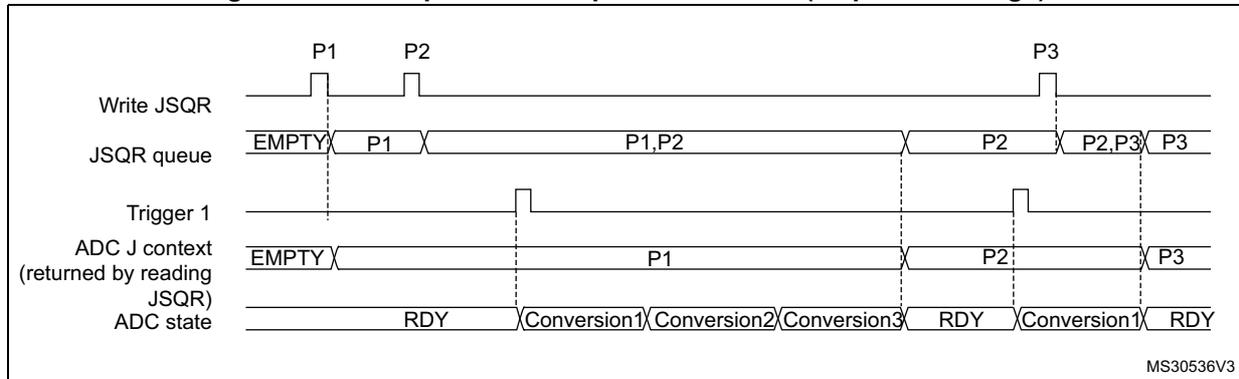
The diagram illustrates the timing of the JSQR queue and ADC state during sequence changes. The top row shows 'Write JSQR' pulses for sequences P1, P2, and P3. The 'JSQR queue' row shows the queue's content: it starts as 'EMPTY', becomes 'P1' after the first write, 'P1,P2' after the second, 'P2' after the third, and 'P2,P3' after the fourth. The 'Trigger 1' row shows hardware triggers. The 'ADC J context (returned by reading JSQR)' row shows the context being processed: it starts as 'EMPTY', then 'P1', then 'P2', and finally 'P3'. The bottom row shows the 'ADC state', which transitions from 'RDY' to 'Conversion1', 'Conversion2', 'Conversion3', back to 'RDY', then 'Conversion1', and finally 'RDY'.
- 1. Parameters:
P1: sequence of 3 conversions, hardware trigger 1
P2: sequence of 1 conversion, hardware trigger 1
P3: sequence of 4 conversions, hardware trigger 1
Figure 156. Example of JSQR queue of context (trigger change)
The diagram illustrates the state of the JSQR queue and ADC context.
-
Write JSQR:
Pulses for parameters P1, P2, and P3.
-
JSQR queue:
Starts as
EMPTY
. After P1, it contains
P1
. After P2, it contains
P1,P2
. When P3 is written, the queue would normally contain
P2,P3
, but the entry for P3 is
Ignored
because the queue is already full with P1 and P2.
-
Trigger 1:
Hardware trigger for P1. It is active when the queue contains P1.
-
Trigger 2:
Hardware trigger for P2. It is
Ignored
when the queue contains P1. It becomes active when the queue contains P2.
-
ADC J context (returned by reading JSQR):
Starts as
EMPTY
. It follows the queue:
P1
when P1 is active,
P2
when P2 is active, and
P3
when P3 is active.
-
ADC state:
Starts as
RDY
. It becomes
Conversion1
when P1 is active, then
Conversion2
. When P2 becomes active, it returns to
RDY
, then becomes
Conversion1
again when P3 is active, and finally returns to
RDY
.
- Parameters:
P1: sequence of 2 conversions, hardware trigger 1
P2: sequence of 1 conversion, hardware trigger 2
P3: sequence of 4 conversions, hardware trigger 1
Queue of context: Behavior when a queue overflow occurs
The Figure 157 and Figure 158 show the behavior of the context Queue if an overflow occurs before or during a conversion.
Figure 157. Example of JSQR queue of context with overflow before conversion
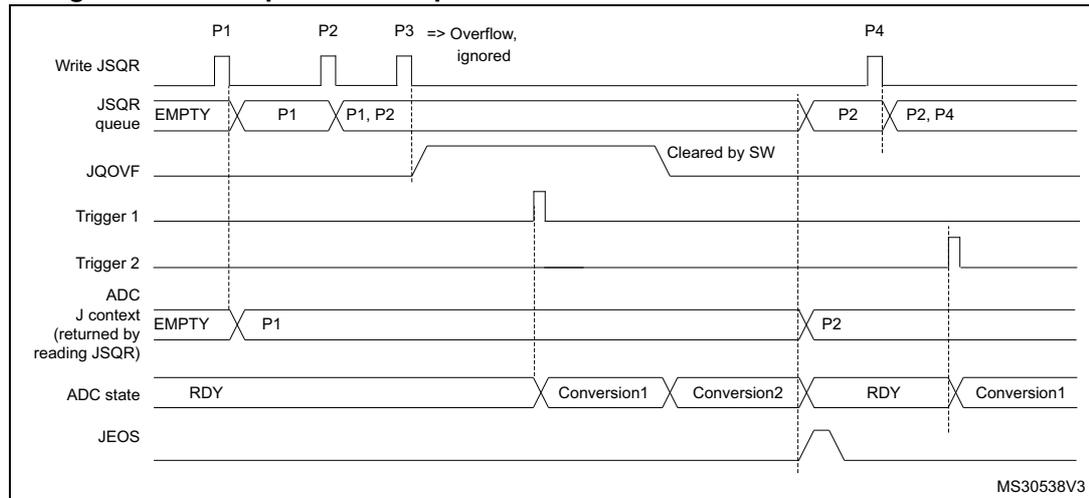
The diagram illustrates the behavior during a queue overflow.
-
Write JSQR:
Pulses for P1, P2, P3, and P4.
-
JSQR queue:
Starts as
EMPTY
. It contains
P1
, then
P1,P2
. When P3 is written, it results in
=> Overflow, ignored
. The queue then contains
P2
, and after P4 is written, it contains
P2,P4
.
-
JQOVF:
An overflow flag that is set when P3 is ignored and cleared by software (
Cleared by SW
).
-
Trigger 1:
Hardware trigger for P1 and P4.
-
ADC J context:
Starts as
EMPTY
. It contains
P1
when P1 is active,
P2
when P2 is active, and
P4
when P4 is active.
-
ADC state:
Starts as
RDY
. It becomes
Conversion1
and
Conversion2
when P1 is active. When P2 becomes active, it returns to
RDY
. When P4 becomes active, it becomes
Conversion1
and returns to
RDY
.
-
JEOS:
End of conversion signal that pulses when the conversion for P4 completes.
- Parameters:
P1: sequence of 2 conversions, hardware trigger 1
P2: sequence of 1 conversion, hardware trigger 2
P3: sequence of 3 conversions, hardware trigger 1
P4: sequence of 4 conversions, hardware trigger 1
Figure 158. Example of JSQR queue of context with overflow during conversion
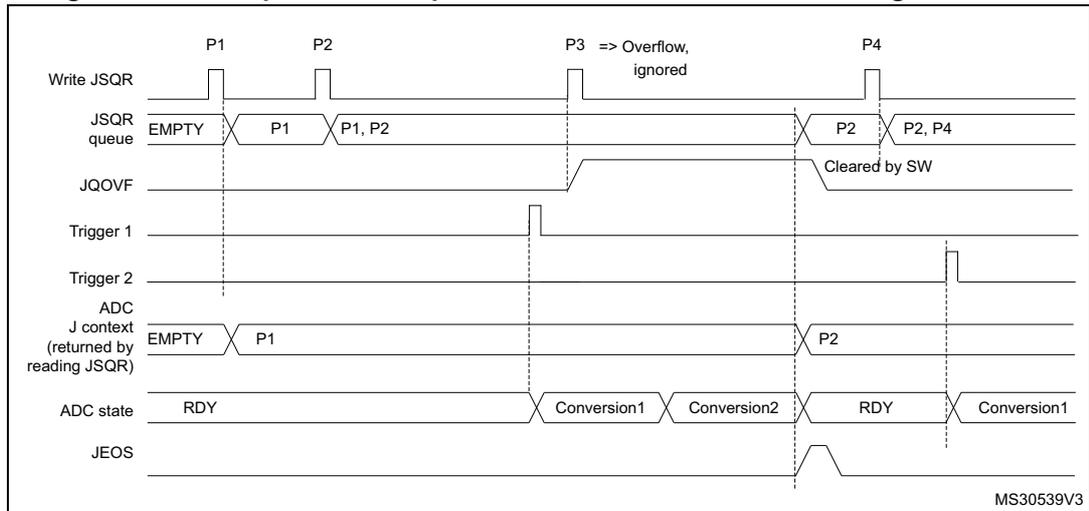
- 1. Parameters:
P1: sequence of 2 conversions, hardware trigger 1
P2: sequence of 1 conversion, hardware trigger 2
P3: sequence of 3 conversions, hardware trigger 1
P4: sequence of 4 conversions, hardware trigger 1
It is recommended to manage the queue overflows as described below:
- • After each P context write into JSQR register, flag JQOVF shows if the write has been ignored or not (an interrupt can be generated).
- • Avoid Queue overflows by writing the third context (P3) only once the flag JEOS of the previous context P2 has been set. This ensures that the previous context has been consumed and that the queue is not full.
Queue of context: Behavior when the queue becomes empty
Figure 159 and Figure 160 show the behavior of the context Queue when the Queue becomes empty in both cases JQM=0 or 1.
Figure 159. Example of JSQR queue of context with empty queue (case JQM=0)
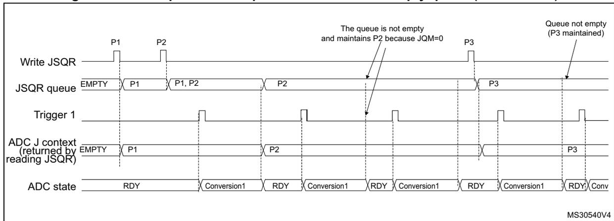
- 1. Parameters:
P1: sequence of 1 conversion, hardware trigger 1
P2: sequence of 1 conversion, hardware trigger 1
P3: sequence of 1 conversion, hardware trigger 1
Note: When writing P3, the context changes immediately. However, because of internal resynchronization, there is a latency and if a trigger occurs just after or before writing P3, it can happen that the conversion is launched considering the context P2. To avoid this situation, the user must ensure that there is no ADC trigger happening when writing a new context that applies immediately.
Figure 160. Example of JSQR queue of context with empty queue (case JQM=1)
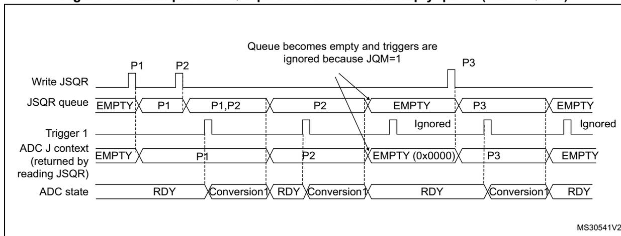
The diagram shows the following signals and states over time:
- Write JSQR: Shows pulses for writing contexts P1, P2, and P3.
- JSQR queue: Shows the queue contents: EMPTY, P1, P1,P2, P2, EMPTY, P3, EMPTY. An arrow points to the EMPTY state with the text "Queue becomes empty and triggers are ignored because JQM=1".
- Trigger 1: Shows hardware trigger pulses. Two pulses occurring while the queue is EMPTY are labeled "Ignored".
- ADC J context (returned by reading JSQR): Shows the context returned: EMPTY, P1, P2, EMPTY (0x0000), P3, EMPTY.
- ADC state: Shows states: RDY, Conversion, RDY, Conversion, RDY, Conversion, RDY.
MS30541V2
- Parameters:
P1: sequence of 1 conversion, hardware trigger 1
P2: sequence of 1 conversion, hardware trigger 1
P3: sequence of 1 conversion, hardware trigger 1
Flushing the queue of context
The figures below show the behavior of the context Queue in various situations when the queue is flushed.
Figure 161. Flushing JSQR queue of context by setting JADSTP=1 (JQM=0). Case when JADSTP occurs during an ongoing conversion.
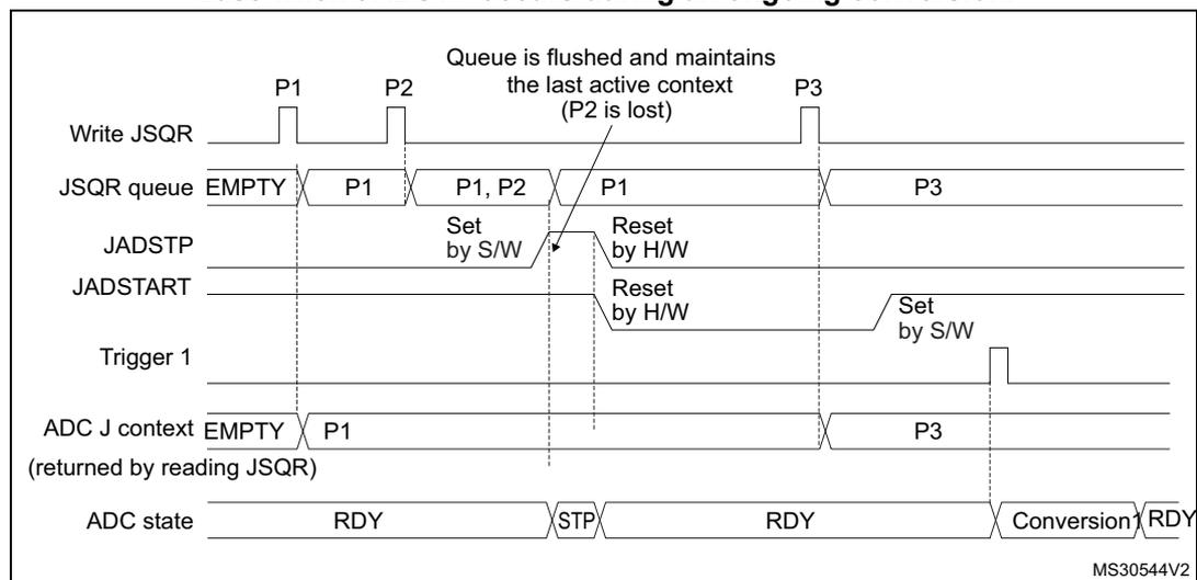
The diagram shows the following signals and states over time:
- Write JSQR: Shows pulses for writing contexts P1, P2, and P3.
- JSQR queue: Shows the queue contents: EMPTY, P1, P1, P2, P1, P3. An arrow points to the P1 state after P2 is lost with the text "Queue is flushed and maintains the last active context (P2 is lost)".
- JADSTP: Shows the JADSTP signal being set by software (S/W) and reset by hardware (H/W).
- JADSTART: Shows the JADSTART signal being reset by hardware (H/W) and set by software (S/W).
- Trigger 1: Shows hardware trigger pulses.
- ADC J context (returned by reading JSQR): Shows the context returned: EMPTY, P1, P3.
- ADC state: Shows states: RDY, STP, RDY, Conversion, RDY.
MS30544V2
- Parameters:
P1: sequence of 1 conversion, hardware trigger 1
P2: sequence of 1 conversion, hardware trigger 1
P3: sequence of 1 conversion, hardware trigger 1
Figure 162. Flushing JSQR queue of context by setting JADSTP=1 (JQM=0).
Case when JADSTP occurs during an ongoing conversion and a new trigger occurs.
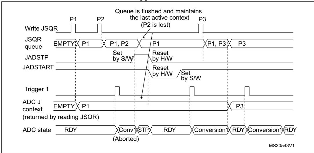
Timing diagram for Figure 162. The diagram shows the following signals and states over time:
- Write JSQR: Shows the sequence of writes to the JSQR register. P1 is written, then P2, then P1 again, and finally P3.
- JSQR queue: Shows the queue of contexts. It starts as EMPTY, then contains P1, then P1 and P2. When P3 is written, the queue contains P1, P2, and P3. However, when JADSTP is set, the queue is flushed and only P1 remains. When P3 is written again, the queue contains P1 and P3.
- JADSTP: Shows the JADSTP bit being set by software (S/W) and reset by hardware (H/W).
- JADSTART: Shows the JADSTART bit being reset by hardware (H/W) and set by software (S/W).
- Trigger 1: Shows the hardware trigger signal.
- ADC J context (returned by reading JSQR): Shows the context returned by reading the JSQR register. It starts as EMPTY, then contains P1. When JADSTP is set, it contains P1. When P3 is written, it contains P3.
- ADC state: Shows the state of the ADC. It starts as RDY. When P1 is written and JADSTART is set, it becomes Conv1. When JADSTP is set, it becomes STP (Aborted). When JADSTART is reset, it becomes RDY. When P3 is written and JADSTART is set, it becomes Conversion1. When the conversion is complete, it becomes RDY.
MS30543V1
- 1. Parameters:
P1: sequence of 1 conversion, hardware trigger 1
P2: sequence of 1 conversion, hardware trigger 1
P3: sequence of 1 conversion, hardware trigger 1
Figure 163. Flushing JSQR queue of context by setting JADSTP=1 (JQM=0).
Case when JADSTP occurs outside an ongoing conversion
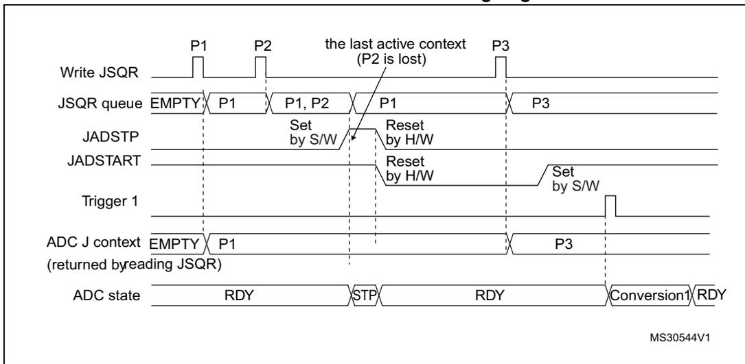
Timing diagram for Figure 163. The diagram shows the following signals and states over time:
- Write JSQR: Shows the sequence of writes to the JSQR register. P1 is written, then P2, then P1 again, and finally P3.
- JSQR queue: Shows the queue of contexts. It starts as EMPTY, then contains P1, then P1 and P2. When P3 is written, the queue contains P1, P2, and P3. However, when JADSTP is set, the queue is flushed and only P1 remains. When P3 is written again, the queue contains P3.
- JADSTP: Shows the JADSTP bit being set by software (S/W) and reset by hardware (H/W).
- JADSTART: Shows the JADSTART bit being reset by hardware (H/W) and set by software (S/W).
- Trigger 1: Shows the hardware trigger signal.
- ADC J context (returned by reading JSQR): Shows the context returned by reading the JSQR register. It starts as EMPTY, then contains P1. When JADSTP is set, it contains P1. When P3 is written, it contains P3.
- ADC state: Shows the state of the ADC. It starts as RDY. When P1 is written and JADSTART is set, it becomes STP. When JADSTART is reset, it becomes RDY. When P3 is written and JADSTART is set, it becomes Conversion1. When the conversion is complete, it becomes RDY.
MS30544V1
- 1. Parameters:
P1: sequence of 1 conversion, hardware trigger 1
P2: sequence of 1 conversion, hardware trigger 1
P3: sequence of 1 conversion, hardware trigger 1
Figure 164. Flushing JSQR queue of context by setting JADSTP=1 (JQM=1)
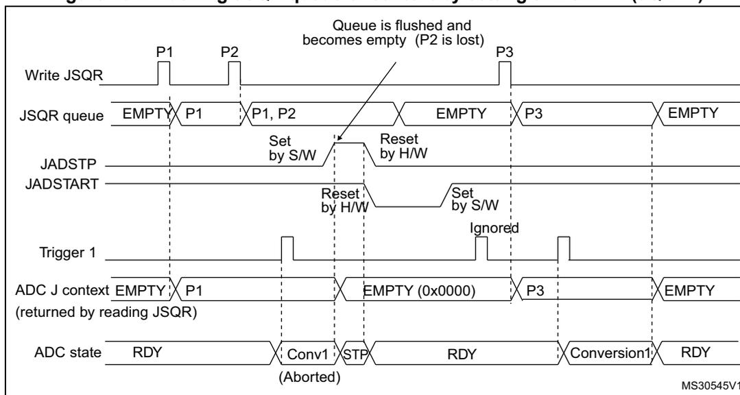
The diagram illustrates the sequence of events for flushing the JSQR queue. The top signal, 'Write JSQR', shows three pulses labeled P1, P2, and P3. The 'JSQR queue' starts as 'EMPTY', becomes 'P1', then 'P1, P2'. When 'JADSTP' is 'Set by S/W', the queue is flushed and becomes 'EMPTY' (P2 is lost). When 'JADSTP' is 'Reset by H/W', the queue becomes 'EMPTY' again. When 'JADSTP' is 'Set by S/W' again, the queue becomes 'P3'. When 'JADSTP' is 'Reset by H/W', the queue becomes 'EMPTY'. The 'ADC J context' (returned by reading JSQR) shows 'EMPTY', 'P1', 'EMPTY (0x0000)', 'P3', and 'EMPTY'. The 'ADC state' shows 'RDY', 'Conv1 (Aborted)', 'STP', 'RDY', 'Conversion1', and 'RDY'. The 'Trigger 1' signal is shown as a pulse. The text 'Queue is flushed and becomes empty (P2 is lost)' is present. The diagram is labeled MS30545V1.
- 1. Parameters:
P1: sequence of 1 conversion, hardware trigger 1
P2: sequence of 1 conversion, hardware trigger 1
P3: sequence of 1 conversion, hardware trigger 1
Figure 165. Flushing JSQR queue of context by setting ADDIS=1 (JQM=0)
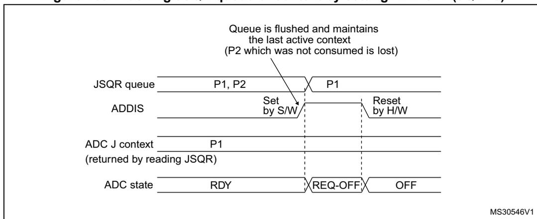
The diagram illustrates the sequence of events for flushing the JSQR queue. The 'JSQR queue' starts as 'P1, P2'. When 'ADDIS' is 'Set by S/W', the queue becomes 'P1'. When 'ADDIS' is 'Reset by H/W', the queue becomes 'P1'. The 'ADC J context' (returned by reading JSQR) shows 'P1'. The 'ADC state' shows 'RDY', 'REQ-OFF', and 'OFF'. The text 'Queue is flushed and maintains the last active context (P2 which was not consumed is lost)' is present. The diagram is labeled MS30546V1.
- 1. Parameters:
P1: sequence of 1 conversion, hardware trigger 1
P2: sequence of 1 conversion, hardware trigger 1
P3: sequence of 1 conversion, hardware trigger 1
Figure 166. Flushing JSQR queue of context by setting ADDIS=1 (JQM=1)
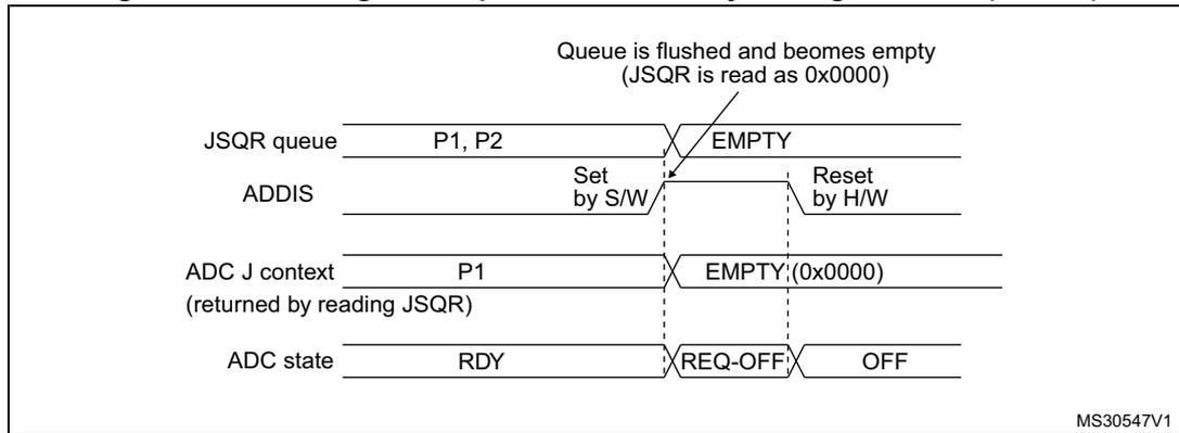
Queue is flushed and becomes empty (JSQR is read as 0x0000)
JSQR queue: P1, P2 → EMPTY
ADDIS: Set by S/W → Reset by H/W
ADC J context (returned by reading JSQR): P1 → EMPTY (0x0000)
ADC state: RDY → REQ-OFF → OFF
MS30547V1
- 1. Parameters:
P1: sequence of 1 conversion, hardware trigger 1
P2: sequence of 1 conversion, hardware trigger 1
P3: sequence of 1 conversion, hardware trigger 1
Queue of context: Starting the ADC with an empty queue
The following procedure must be followed to start ADC operation with an empty queue, in case the first context is not known at the time the ADC is initialized. This procedure is only applicable when JQM bit is reset:
- 5. Write a dummy JSQR with JEXTEN not equal to 0 (otherwise triggering a software conversion)
- 6. Set JADSTART
- 7. Set JADSTP
- 8. Wait until JADSTART is reset
- 9. Set JADSTART.
Disabling the queue
It is possible to disable the queue by setting bit JQDIS=1 into the ADC_CFGR register.
Queue of context: Programming of the register ADC_JSQR
When the injected conversion queue of context is enabled (JQDIS=0), the ADC_JSQR must be programmed at one register write access. As JL[1:0] register define the number of the injected sequence, corresponding JSQ1 to JSQ4 must be written at same time. If ADC_JSQR is reprogrammed before the injected conversion start, reprogrammed data is put on the queue. When queue of context is empty, ADC_JSQR read back as 0x0000. Register access should not use the 'read modify write' sequence.
When ADC_JSQR is programmed when already two contexts are queued, it raises JQOVF flag and generate the interrupt.
26.4.23 Programmable resolution (RES) - fast conversion mode
It is possible to perform faster conversion by reducing the ADC resolution.
The resolution can be configured to be either 16, 14, 12, 10, 8 bits by programming the control bits RES[1:0]. Figure 171 , Figure 172 , Figure 173 and Figure 174 show the conversion result format with respect to the resolution as well as to the data alignment.
Lower resolution allows faster conversion time for applications where high-data precision is not required. It reduces the conversion time spent by the successive approximation steps according to Table 216 .
Table 216. \( T_{SAR} \) timings depending on resolution
| RES [2:0] | \( T_{SAR} \) (ADC clock cycles) | \( T_{SAR} \) (ns) at \( F_{adc\_ker\_ck}=24 \) MHz | \( T_{adc\_ker\_ck} \) (ADC clock cycles) (with Sampling Time= 1.5 ADC clock cycles) | \( T_{adc\_ker\_ck} \) (ns) at \( F_{adc\_ker\_ck}=24 \) MHz |
|---|---|---|---|---|
| 16 bits | 8.5 ADC clock cycles | 354.2 | 10 ADC clock cycles | 416.7 |
| 14 bits | 7.5 ADC clock cycles | 312.5 | 9 ADC clock cycles | 375 |
| 12 bits | 6.5 ADC clock cycles | 270.8 | 8 ADC clock cycles | 333.3 |
| 10 bits | 5.5 ADC clock cycles | 229.2 | 7 ADC clock cycles | 291.7 |
| 8 bits | 4.5 ADC clock cycles | 187.5 | 6 ADC clock cycles | 250.0 |
26.4.24 End of conversion, end of sampling phase (EOC, JEOC, EOSMP)
The ADC notifies the application for each end of regular conversion (EOC) event and each injected conversion (JEOC) event.
The ADC sets the EOC flag as soon as a new regular conversion data is available in the ADC_DR register. An interrupt can be generated if bit EOCIE is set. EOC flag is cleared by the software either by writing 1 to it or by reading ADC_DR.
The ADC sets the JEOC flag as soon as a new injected conversion data is available in one of the ADC_JDRy register. An interrupt can be generated if bit JEOCIE is set. JEOC flag is cleared by the software either by writing 1 to it or by reading the corresponding ADC_JDRy register.
The ADC also notifies the end of Sampling phase by setting the status bit EOSMP (for regular conversions only). EOSMP flag is cleared by software by writing 1 to it. An interrupt can be generated if bit EOSMPIE is set.
26.4.25 End of conversion sequence (EOS, JEOS)
The ADC notifies the application for each end of regular sequence (EOS) and for each end of injected sequence (JEOS) event.
The ADC sets the EOS flag as soon as the last data of the regular conversion sequence is available in the ADC_DR register. An interrupt can be generated if bit EOSIE is set. EOS flag is cleared by the software either by writing 1 to it.
The ADC sets the JEOS flag as soon as the last data of the injected conversion sequence is complete. An interrupt can be generated if bit JEOSIE is set. JEOS flag is cleared by the software either by writing 1 to it.
26.4.26 Timing diagrams example (single/continuous modes, hardware/software triggers)
Figure 167. Single conversions of a sequence, software trigger
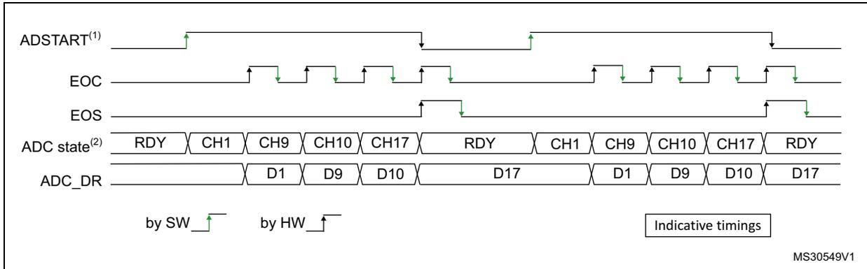
- 1. EXTEN=0x0, CONT=0
- 2. Channels selected = 1,9, 10, 17; AUTDLY=0.
Figure 168. Continuous conversion of a sequence, software trigger
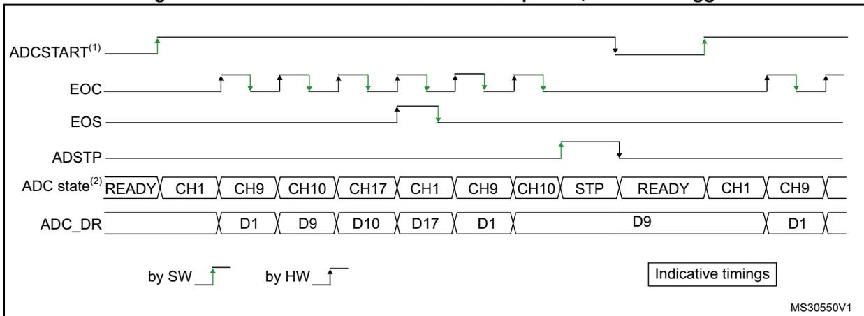
- 1. EXTEN=0x0, CONT=1
- 2. Channels selected = 1,9, 10, 17; AUTDLY=0.
Figure 169. Single conversions of a sequence, hardware trigger
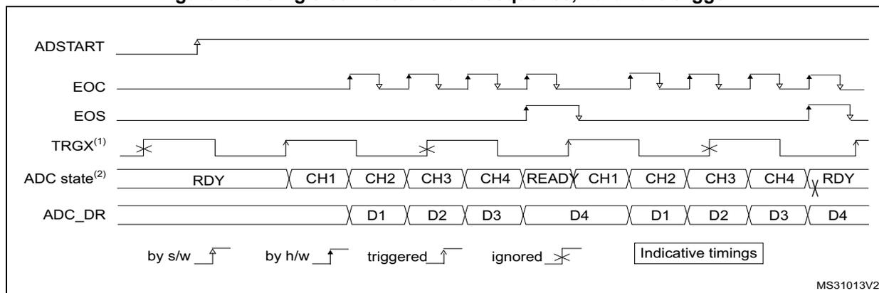
MS31013V2
- 1. TRGX (over-frequency) is selected as trigger source, EXTEN = 01, CONT = 0
- 2. Channels selected = 1, 2, 3, 4; AUTDLY=0.
Figure 170. Continuous conversions of a sequence, hardware trigger
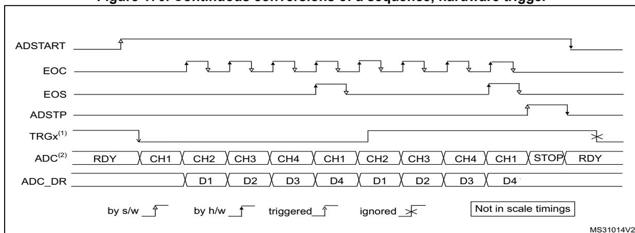
MS31014V2
- 1. TRGX is selected as trigger source, EXTEN = 10, CONT = 1
- 2. Channels selected = 1, 2, 3, 4; AUTDLY=0.
26.4.27 Data management
Data register, data alignment and offset (ADC_DR, ADC_JDRy, OFFSETy, OFFSETy_CH, OVSS, LSHIFT, RSHIFT, SSATE)
Data and alignment
At the end of each regular conversion channel (when EOC event occurs), the result of the converted data is stored into the ADC_DR data register which is 32 bits wide.
At the end of each injected conversion channel (when JEOC event occurs), the result of the converted data is stored into the corresponding ADC_JDRy data register which is 32 bits wide.
The OVSS[3:0] and LSHIFT[3:0] bitfields in the ADC_CFGR2 register selects the alignment of the data stored after conversion. Data can be right- or left-aligned as shown in Figure 171 , Figure 172 , Figure 173 and Figure 174 .
Note: The data can be re-aligned in normal and in oversampling mode.
Offset
An offset \( y \) ( \( y=1, 2, 3, 4 \) ) can be applied to a channel by programming a value different from 0 in OFFSET \( y \) [25:0] bitfield into ADC_OFR \( y \) register. The channel to which the offset is applied is programmed into the bits OFFSET \( y\_CH \) [4:0] of ADC_OFR \( y \) register. In this case, the converted value is decreased by the user-defined offset written in the bits OFFSET \( y \) [25:0]. The result may be a negative value so the read data is signed and the SEXT bit represents the extended sign value.
The offset value should be lower than the max conversion value (ex. 16bit mode, offset value max is 0xFFFF).
The offset correction is also supported in oversampling mode. For the oversampling mode, offset is subtracted before OVSS right shift applied.
Table 217 describes how the comparison is performed for all the possible resolutions for analog watchdog 1, 2, 3.
Table 217. Offset computation versus data resolution
| Resolution (bits RES[2:0]) | Subtraction between raw converted data and offset: | Result | Comments | |
|---|---|---|---|---|
| Raw converted Data, left aligned | Offset | |||
| 16 bits | DATA[15:0] | OFFSET[25:0] | signed 27-bit data | - |
| 14 bits | DATA[15:2],00 | OFFSET[25:0] | signed 27-bit data | The user must configure OFFSET[1:0] to 00 |
| 12 bits | DATA[15:4],00 00 | OFFSET[25:0] | signed 27-bit data | The user must configure OFFSET[3:0] to 0000 |
| 10 bits | DATA[15:6],00 0000 | OFFSET[25:0] | signed 27-bit data | The user must configure OFFSET[5:0] to 000000 |
| 8 bits | DATA[15:8],00 0000 | OFFSET[25:0] | signed 27-bit data | The user must configure OFFSET[7:0] to 00000000 |
When reading data from ADC_DR (regular channel) or from ADC_JDR \( y \) (injected channel, \( y=1,2,3,4 \) ), the offset compensation is disabled when ADC_OFR \( y \) [25:0] bitfield is reset. Otherwise, the offset for ADC_OFR \( y \) [30:26] channel is enabled.
Figure 171 , Figure 172 , Figure 173 and Figure 174 show alignments for signed and unsigned data together with corresponding OVSS and LSHIFT values.
Figure 171. Right alignment (offset disabled, unsigned value)
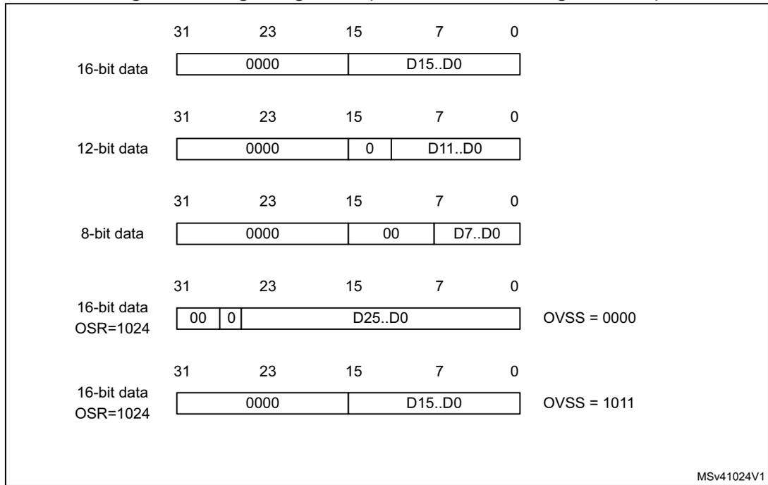
Figure 171 illustrates the right alignment of ADC data when offset is disabled and the value is unsigned. The diagram shows five examples of data alignment within a 32-bit register, with bit positions 31, 23, 15, 7, and 0 marked at the top.
- 16-bit data: The 16-bit value D15..D0 is aligned to the right, occupying bits 15..0. Bits 31..16 are set to 0000.
- 12-bit data: The 12-bit value D11..D0 is aligned to the right, occupying bits 11..0. Bits 31..12 are set to 0000, with a 0 in bit 11.
- 8-bit data: The 8-bit value D7..D0 is aligned to the right, occupying bits 7..0. Bits 31..8 are set to 0000, with 00 in bits 7..0.
- 16-bit data OSR=1024: With oversampling, a 25-bit value D25..D0 is produced. It is right-aligned, occupying bits 25..0. Bits 31..26 are set to 00, with a 0 in bit 25.
- 16-bit data OSR=1024 (OVSS = 1011): With oversampling and a non-zero offset (OVSS = 1011), a 16-bit value D15..D0 is produced. It is right-aligned, occupying bits 15..0. Bits 31..16 are set to 0000.
MSv41024V1
Figure 172. Right alignment (offset enabled, signed value)
Figure 172 illustrates the right alignment of ADC data when offset is enabled and the value is signed. The diagram shows six examples of data alignment within a 32-bit register, with bit positions 31, 23, 15, 7, and 0 marked at the top. A vertical dashed line at bit 15 indicates the sign bit position for 16-bit values.
- 16-bit data: The 16-bit value D15..D0 is right-aligned and sign-extended (SEXT) to fill the 32-bit register. This results in a Signed 32-bit format .
- 16-bit data: The 16-bit value D14..D0 is right-aligned and sign-extended (SEXT) to fill the 32-bit register. This results in a Signed 16-bit format . This configuration is used when SSATE = 1 OR RSHIFT1..4 = 1 .
- 12-bit data: The 12-bit value D11..D0 is right-aligned and sign-extended (SEXT) to fill the 32-bit register.
- 8-bit data: The 8-bit value D7..D0 is right-aligned and sign-extended (SEXT) to fill the 32-bit register.
- 8-bit data: The 8-bit value D6..D0 is right-aligned and sign-extended (SEXT) to fill the 32-bit register. This results in a Signed 8-bit format . This configuration is used when SSATE = 1 OR RSHIFT1..4 = 1 .
- 16-bit data OSR=1024: With oversampling, a 25-bit value D25..D0 is produced. It is right-aligned and sign-extended (SEXT) to fill the 32-bit register. This results in a Signed 32-bit format when OVSS = 0000 .
MSv41025V1
Figure 173. Left alignment (offset disabled, unsigned value)
Figure 173 illustrates the left alignment of unsigned values in a 32-bit register. The register bits are numbered 31, 23, 15, 7, and 0. The data is aligned to the left, and the remaining bits are zero-filled.
| Data Type | Bit Range | LSHIFT |
|---|---|---|
| 16-bit data | D15..D0 | 0 |
| 12-bit data | D11..D0 | 4 |
| 8-bit data | D7..D0 | 0 |
| 16-bit data OSR=1024 | D25..D0 | 6 |
MSv41026V1
Figure 174. Left alignment (offset enabled, signed value)
Figure 174 illustrates the left alignment of signed values in a 32-bit register. The register bits are numbered 31, 23, 15, 7, and 0. The data is aligned to the left, and the remaining bits are zero-filled. The 'S' bit at bit 31 indicates the sign bit.
| Data Type | Bit Range | LSHIFT | Format |
|---|---|---|---|
| 16-bit data | D15..D0 | 15 | Signed 32-bit format |
| 16-bit data | D14..D0 | SATEN = 1 | Signed 16-bit format |
| 12-bit data | D11..D0 | 3 | Signed 16-bit format |
| 8-bit data | D7..D0 | 7 | Signed 16-bit format |
| 8-bit data | D6..D0 | SSATE = 1 OR RSHIFT1..4 = 1 | Signed 8-bit format |
| 16-bit data OSR=1024 | D25..D0 | 5 | Signed 32-bit format |
MSv41027V2
16-bit and 8-bit signed format management: RSHIFTx,SSATE
The offset correction sign-extends the data format, resulting in an unsigned 16-bit conversion being extended to 17-bit signed format, for instance.
Three options are offered for formatting 8-bit and 16-bit conversion results.
For each offset correction channel 1 to 4, a RSHIFT1..4 bit in the ADC_CFGR2 register allows to have the result right-shifted 1-bit and have it fitting a standard 8 or 16-bit format.
Another option is to have the result saturated to the 16-bit and 8-bit signed formats, for the following cases only: RES[2:0] = 000 (16-bit format) and RES[2:0] = 111 (8-bit format).
This mode is enabled with the SSATE bit in the ADC_OFRy register.
The table below summarizes the 3 available use case for 16-bit format.
Table 218. 16-bit data formats
| SSATE | RSHIFTx | Format | Data range (offset = 0x8000) |
|---|---|---|---|
| 0 | 0 | Sign-extended 17-bit significant data SEXT[31:16] DATA[15:0] | 0x00007FFF - 0x FFFF8000 |
| 0 | 1 | Sign-extended right-shifted 16-bit significant data SEXT[31:15] DATA[14:0] | 0x3FFF - 0xC000 |
| 1 | 0 | Sign-extended saturated 16-bit significant data SEXT[31:15] DATA[14:0] | 7FFF - 0x8000 |
| 1 | 1 | Reserved | - |
Numerical examples are given in Table 219 with 3 different offset values.
Table 219. Numerical examples for 16-bit format (bold indicates saturation)
| Raw conversion result | Offset value | Result SSATE = 0 RSHIFT = 0 | Result SSATE = 0 RSHIFT = 1 | Result SSATE = 1 RSHIFT = 0 |
|---|---|---|---|---|
| 0xFFFF | 0x8000 | 0x0000 7FFF | 3FFF | 7FFF |
| 0x8000 | 0x0000 0000 | 0 | 0 | |
| 0x0000 | 0xFFFF 8000 | C000 | 8000 | |
| 0xFFFF | 0x8020 | 0x0000 7FDF | 3FEF | 7FDF |
| 0x8000 | 0xFFFF FFE0 | FFF0 | FFE0 | |
| 0x0000 | 0xFFFF 7FE0 | BFF0 | 8000 | |
| 0xFFFF | 0x7FF0 | 0x0000 800F | 4007 | 7FFF |
| 0x8000 | 0x0000 0010 | 8 | 0010 | |
| 0x0000 | 0xFFFF 8010 | C008 | 8010 |
When oversampling mode is active, the SSATE and RSHIFT1..4 bits are not supported.
ADC overrun (OVR, OVRMOD)
The overrun flag (OVR) notifies of a buffer overrun event when the regular converted data has not been read (by the CPU or the DMA) before ADC_DR FIFO (eight stages) is overflowed.
The OVR flag is set when a new conversion completes while ADC_CR register FIFO was full. An interrupt is generated if OVRRIE bit is set to 1.
When an overrun condition occurs, the ADC is still operating and can continue to convert unless the software decides to stop and reset the sequence by setting ADSTP to 1.
OVR flag is cleared by software by writing 1 to it.
Data can be configured to be preserved or overwritten when an overrun event occurs by programming the OVRMOD control bit of the ADC_CFGR register:
- • OVRMOD = 0
The overrun event preserves the data register from being overwritten: the old data is maintained up to ADC_DR FIFO depth (8 data) and the new conversion is discarded and lost. If OVR remains at 1, any further conversion is performed but the resulting data is also discarded.
- • OVRMOD = 1
The data register is overwritten with the last conversion result and the previous unread data is lost. In this mode, ADC_DR FIFO is disabled. If OVR remains at 1, any further conversion is performed normally and the ADC_DR register always contains the latest converted data.
Figure 175. Example of overrun (OVRMOD = 0)
Timing diagram for Figure 175. Example of overrun (OVRMOD = 0). The diagram shows the following signals and states over time:
- ADSTART : Software trigger (s/w) at the beginning, hardware trigger (h/w) later, and a stop signal at the end.
- EOC : End of Conversion signals for each channel.
- OVR : Overrun flag, which goes high when a new conversion starts before the previous data is read from the FIFO.
- ADSTP : Stop conversion signal.
- TRGx : External trigger signal.
- ADC state : RDY → CH1 → CH2 → CH3 → CH4 → ... → CH11 → CH12 → CH13 → STOP → RDY.
- ADC_DR read access : Software read accesses for channels CH2, CH3, CH12, and CH13.
- ADC_DR : Data registers showing values D1, D2, D3, D4, D5.
- ADC_DR (FIFO_DATA) : FIFO data registers showing values D4, D5, D9, D10, D10, na, D12. The 'na' (not applicable) indicates a lost conversion due to overrun.
Legend: by s/w ↑, by h/w ↑, triggered ↑. Indicative timings. MSv69549V1
Figure 176. Example of overrun (OVRMOD = 1)
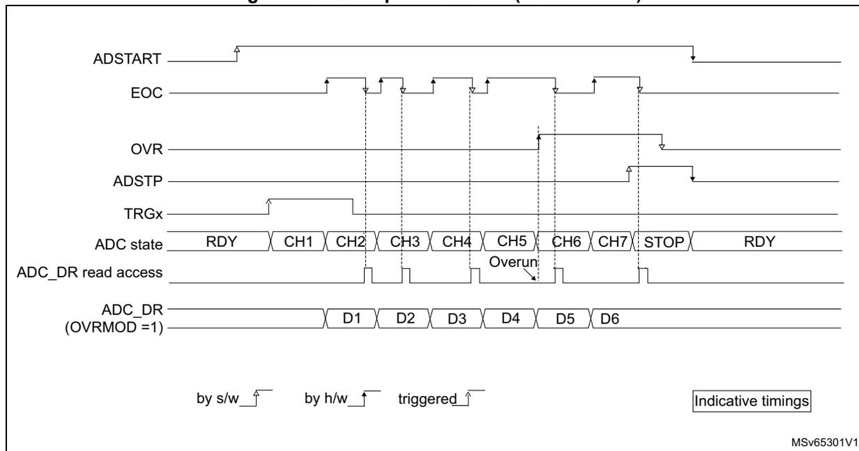
Timing diagram for Figure 176. Example of overrun (OVRMOD = 1). The diagram shows the following signals and states over time:
- ADSTART : Software trigger (s/w) at the beginning, hardware trigger (h/w) later, and a stop signal at the end.
- EOC : End of Conversion signals for each channel.
- OVR : Overrun flag, which goes high when a new conversion starts before the previous data is read from the ADC_DR register.
- ADSTP : Stop conversion signal.
- TRGx : External trigger signal.
- ADC state : RDY → CH1 → CH2 → CH3 → CH4 → CH5 → CH6 → CH7 → STOP → RDY.
- ADC_DR read access : Software read accesses for channels CH2, CH3, CH4, CH5, and CH6. An 'Overrun' label indicates the loss of data for CH5.
- ADC_DR (OVRMOD = 1) : Data registers showing values D1, D2, D3, D4, D5, D6. The data for CH5 is overwritten by CH6.
Legend: by s/w ↑, by h/w ↑, triggered ↑. Indicative timings. MSv65301V1
Note: There is no overrun detection on the injected channels since there is a dedicated data register for each of the four injected channels.
Managing a sequence of conversion without using the DMA
If the conversions are slow enough, the conversion sequence can be handled by the software. In this case the software must use the EOC flag and its associated interrupt to handle each data. Each time a conversion is complete, EOC is set and the ADC_DR register can be read. OVRMOD should be configured to 0 to manage overrun events or FIFO overflows as errors.
Managing conversions without using the DMA and without overrun
It may be useful to let the ADC convert one or more channels without reading the data each time (if there is an analog watchdog for instance). In this case, the OVRMOD bit must be configured to 1 and OVR flag should be ignored by the software. An overrun event does not prevent the ADC from continuing to convert, and the ADC_DR register always contains the latest conversion.
Managing conversions using the DMA
Since converted channel values are stored into a unique data register, it is useful to use DMA for conversion of more than one channel. This avoids the loss of the data already stored in the ADC_DR register.
When the DMA mode is enabled (DMNGT bit = 01 or 11 in the ADC_CFGR register in single ADC mode or MDMA different from 0b00 in dual ADC mode), a DMA request is generated after each conversion of a channel. This allows the transfer of the converted data from the ADC_DR register to the destination location selected by the software.
Despite this, if an overrun occurs (OVR=1) because the DMA could not serve the DMA transfer request in time, the ADC stops generating DMA requests and the data corresponding to the new conversion is not transferred by the DMA. Which means that all the data transferred to the RAM can be considered as valid.
Depending on the configuration of OVRMOD bit, the data is either preserved or overwritten (refer to Section : ADC overrun (OVR, OVRMOD) ).
The DMA transfer requests are blocked until the software clears the OVR bit.
Two different DMA modes are proposed depending on the application use and are configured with bit DMNGT of the ADC_CFGR register in single ADC mode, or with bit DAMDF of the ADCx_CCR register in dual ADC mode:
- • DMA one shot mode (DMNGT bit = 01).
This mode is suitable when the DMA is programmed to transfer a fixed number of data. - • DMA circular mode (DMNGT bit = 11)
This mode is suitable when programming the DMA in circular mode.
DMA one shot mode (DMNGT=01)
In this mode, the ADC generates a DMA transfer request each time a new conversion data is available and stops generating DMA requests once the DMA has reached the last DMA transfer (when a transfer complete interrupt occurs - refer to DMA section) even if a conversion has been started again.
When the DMA transfer is complete (all the transfers configured in the DMA controller have been done):
- • The content of the ADC data register is frozen.
- • Any ongoing conversion is aborted with partial result discarded.
- • No new DMA request is issued to the DMA controller. This avoids generating an overrun error if there are still conversions which are started.
- • Scan sequence is stopped and reset.
- • The DMA is stopped.
DMA circular mode (DMNGT=11)
In this mode, the ADC generates a DMA transfer request each time a new conversion data is available in the data register, even if the DMA has reached the last DMA transfer. This allows configuring the DMA in circular mode to handle a continuous analog input data stream.
DMA with FIFO
The output data register has eight-stage FIFO. Two different DMA requests are generated parallel. When a data is available, "SREQ single request" generated, when 4 data are available, "BREQ burst request" generated. DMA2 can be programmed either single transfer mode or incremental burst mode(4 beats), according to this mode, correct request line is selected by the DMA2. Please refer to the DMA2 chapter for further information.
26.4.28 Managing conversions using the DFSDM
The ADC conversion results can be transferred directly to the Digital Filter for Sigma Delta Modulators (DFSDM).
In this case, the DMNGT[1:0] bits must be set to 10.
The ADC transfers 16 least significant bits of the regular data register data to the DFSDM, which in turns resets the EOC flag once the transfer is effective.
The data format must be 16-bit signed:
ADC_DR[31:16] = don't care
ADC_DR[15] = sign
ADC_DR[14:0] = data
Any value above 16-bit signed format is truncated.
26.4.29 Dynamic low-power features
Auto-delayed conversion mode (AUTDLY)
The ADC implements an auto-delayed conversion mode controlled by the AUTDLY configuration bit. Auto-delayed conversions are useful to simplify the software as well as to optimize performance of an application clocked at low frequency where there would be risk of encountering an ADC overrun.
When AUTDLY=1, a new conversion can start only if all the previous data of the same group has been treated:
- • For a regular conversion: once the ADC_DR register has been read or if the EOC bit has been cleared (see Figure 177 ).
- • For an injected conversion: when the JEOS bit has been cleared (see Figure 178 ).
This is a way to automatically adapt the speed of the ADC to the speed of the system which reads the data.
The delay is inserted after each regular conversion (whatever DISCEN=0 or 1) and after each sequence of injected conversions (whatever JDISCEN=0 or 1).
Note: There is no delay inserted between each conversions of the injected sequence, except after the last one.
During a conversion, a hardware trigger event (for the same group of conversions) occurring during this delay is ignored.
Note: This is not true for software triggers where it remains possible during this delay to set the bits ADSTART or JADSTART to re-start a conversion: it is up to the software to read the data before launching a new conversion.
No delay is inserted between conversions of different groups (a regular conversion followed by an injected conversion or conversely):
- • If an injected trigger occurs during the automatic delay of a regular conversion, the injected conversion starts immediately (see Figure 178 ).
- • Once the injected sequence is complete, the ADC waits for the delay (if not ended) of the previous regular conversion before launching a new regular conversion (see Figure 180 ).
The behavior is slightly different in auto-injected mode (JAUTO=1) where a new regular conversion can start only when the automatic delay of the previous injected sequence of conversion has ended (when JEOS has been cleared). This is to ensure that the software can read all the data of a given sequence before starting a new sequence (see Figure 181 ).
To stop a conversion in continuous auto-injection mode combined with autodelay mode (JAUTO=1, CONT=1 and AUTDLY=1), follow the following procedure:
- 1. Wait until JEOS=1 (no more conversions are restarted)
- 2. Clear JEOS,
- 3. Set ADSTP=1
- 4. Read the regular data.
If this procedure is not respected, a new regular sequence can re-start if JEOS is cleared after ADSTP has been set.
In AUTDLY mode, a hardware regular trigger event is ignored if it occurs during an already ongoing regular sequence or during the delay that follows the last regular conversion of the sequence. It is however considered pending if it occurs after this delay, even if it occurs during an injected sequence of the delay that follows it. The conversion then starts at the end of the delay of the injected sequence.
In AUTDLY mode, a hardware injected trigger event is ignored if it occurs during an already ongoing injected sequence or during the delay that follows the last injected conversion of the sequence.
Figure 177. AUTDLY=1, regular conversion in continuous mode, software trigger
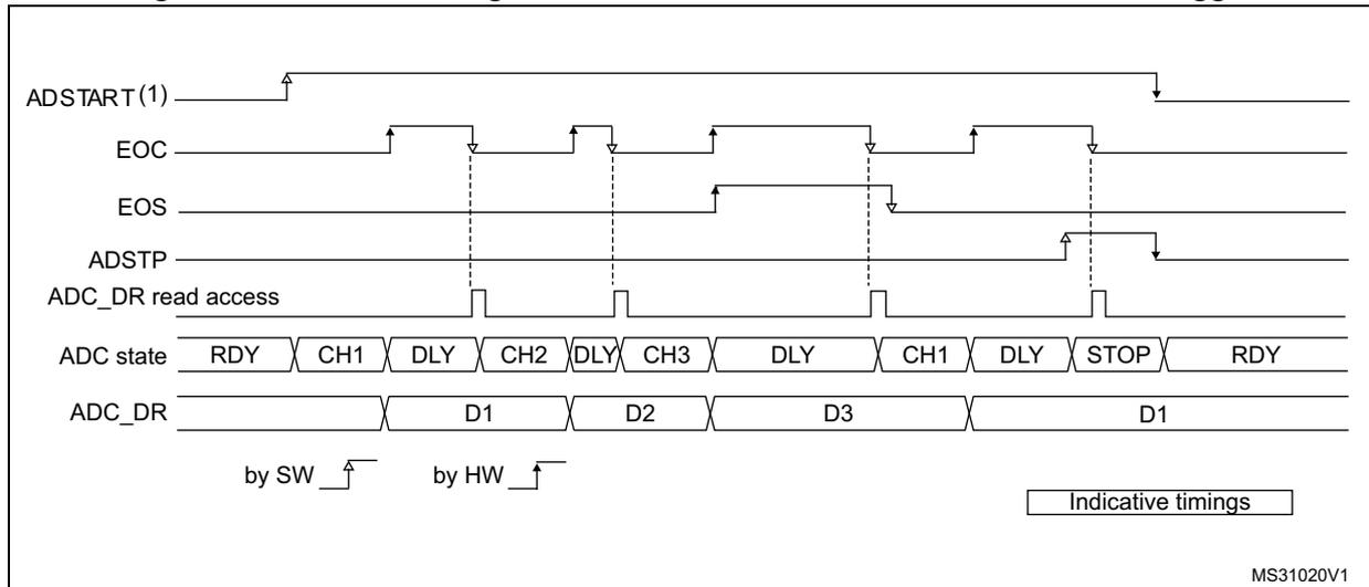
MS31020V1
- 1. AUTDLY=1
- 2. Regular configuration: EXTEN=0x0 (SW trigger), CONT=1, CHANNELS = 1,2,3
- 3. Injected configuration DISABLED
Figure 178. AUTDLY=1, regular HW conversions interrupted by injected conversions (DISCEN=0; JDISCEN=0)
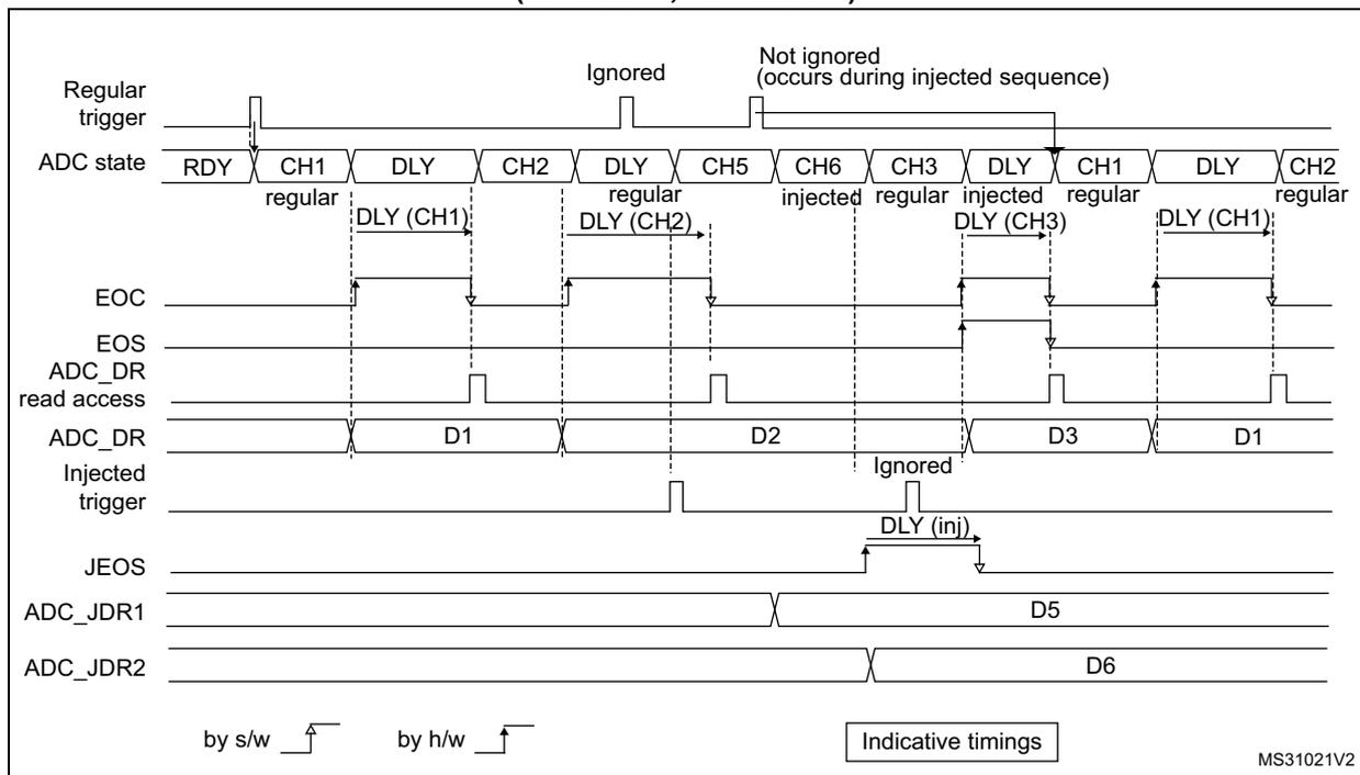
MS31021V2
- 1. AUTDLY=1
- 2. Regular configuration: EXTEN=0x1 (HW trigger), CONT=0, DISCEN=0, CHANNELS = 1, 2, 3
- 3. Injected configuration: JEXTEN=0x1 (HW Trigger), JDISCEN=0, CHANNELS = 5,6
Figure 179. AUTDLY=1, regular HW conversions interrupted by injected conversions (DISCEN=1, JDISCEN=1)
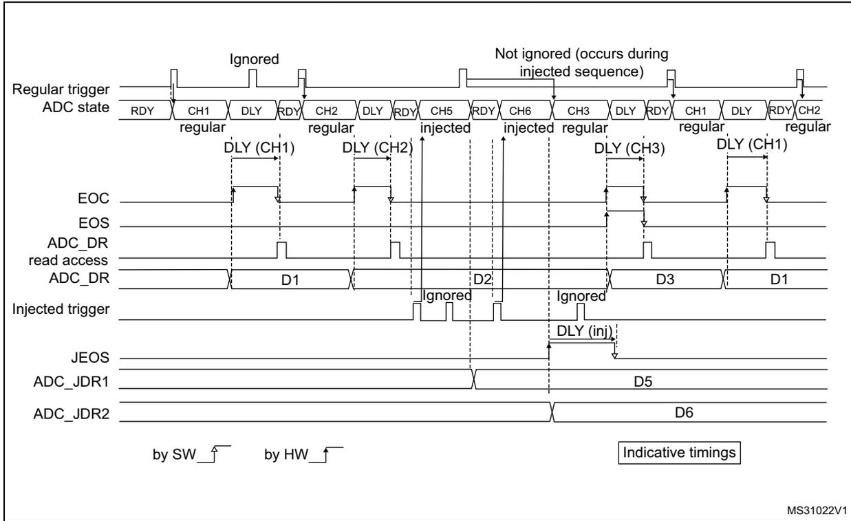
The diagram shows the timing of ADC conversions. The 'Regular trigger' line shows a series of pulses. The 'ADC state' line shows the sequence: RDY, CH1 (regular), DLY, RDY, CH2 (regular), DLY, RDY, CH5 (injected), RDY, CH6 (injected), CH3 (regular), DLY, RDY, CH1 (regular), DLY, RDY, CH2 (regular). The 'EOC' line pulses at the end of each regular sequence. The 'ADC_DR' line shows data D1, D2, D3, D1. The 'Injected trigger' line shows pulses that are ignored during regular sequences. The 'JEOS' line pulses at the end of the injected sequence. The 'ADC_JDR1' and 'ADC_JDR2' lines show data D5 and D6 respectively. Delays DLY(CH1), DLY(CH2), DLY(CH3), and DLY(inj) are indicated. A legend at the bottom shows 'by SW' and 'by HW' trigger symbols. The text 'Indicative timings' is present. The code 'MS31022V1' is in the bottom right corner.
- 1. AUTDLY=1
- 2. Regular configuration: EXTEN=0x1 (HW trigger), CONT=0, DISCEN=1, DISCNUM=1, CHANNELS = 1, 2, 3.
- 3. Injected configuration: JEXTEN=0x1 (HW Trigger), JDISCEN=1, CHANNELS = 5,6
Figure 180. AUTDLY=1, regular continuous conversions interrupted by injected conversions
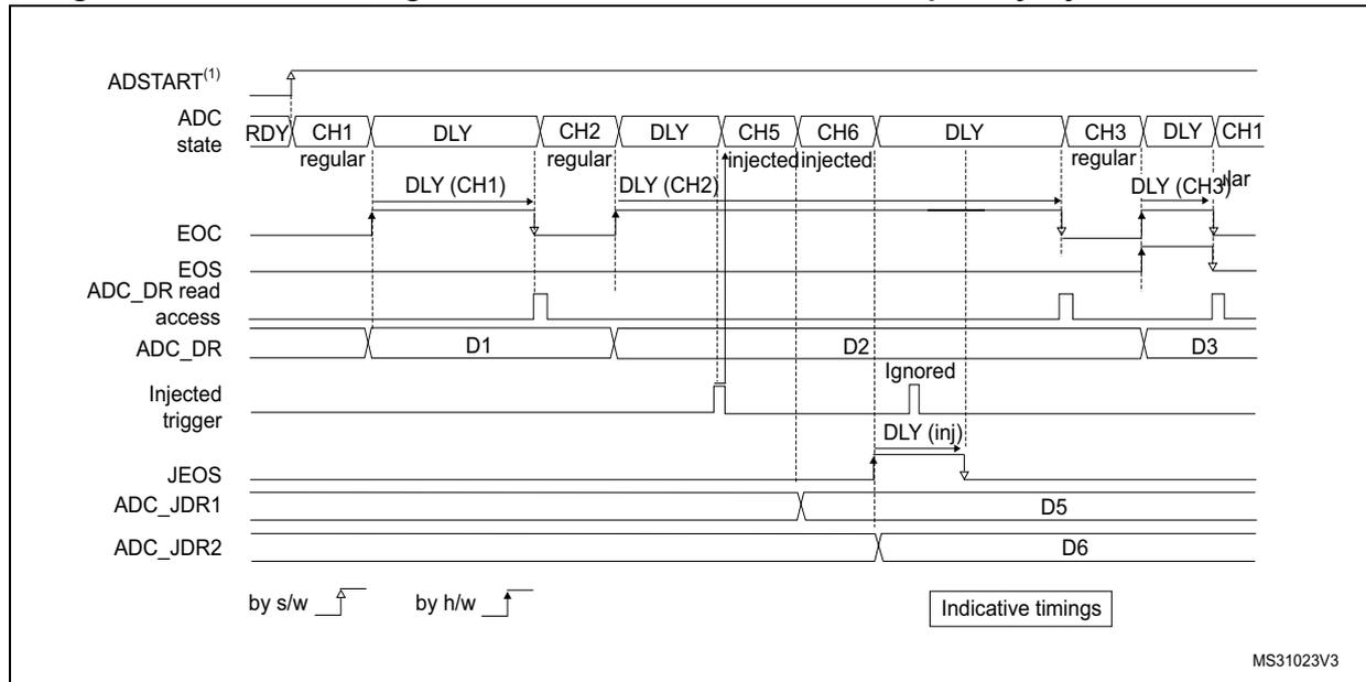
MS31023V3
- 1. AUTDLY=1
- 2. Regular configuration: EXTEN=0x0 (SW trigger), CONT=1, DISCEN=0, CHANNELS = 1, 2, 3
- 3. Injected configuration: JEXTEN=0x1 (HW Trigger), JDISCEN=0, CHANNELS = 5,6
Figure 181. AUTDLY=1 in auto- injected mode (JAUTO=1)
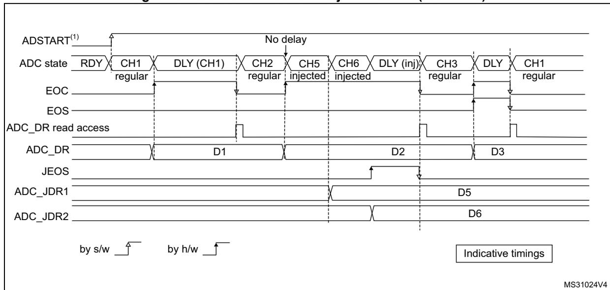
MS31024V4
- 1. AUTDLY=1
- 2. Regular configuration: EXTEN=0x0 (SW trigger), CONT=1, DISCEN=0, CHANNELS = 1, 2
- 3. Injected configuration: JAUTO=1, CHANNELS = 5,6
26.4.30 Analog window watchdog (AWD1EN, JAWD1EN, AWD1SGL, AWD1CH, AWD2CH, AWD3CH, AWD_HTRy, AWD_LTRy, AWDy)
The three AWD analog watchdogs monitor whether some channels remain within a configured voltage range (window).
Figure 182. Analog watchdog guarded area

AWDx flag and interrupt
An interrupt can be enabled for each of the 3 analog watchdogs by setting AWDyIE in the ADC_IER register (x=1,2,3).
AWDy (y=1,2,3) flag is cleared by software by writing 1 to it.
The ADC conversion result is compared to the lower and higher thresholds before alignment.
Description of analog watchdog 1
The AWD analog watchdog 1 is enabled by setting the AWD1EN bit in the ADC_CFGR register. This watchdog monitors whether either one selected channel or all enabled channels (1) remain within a configured voltage range (window).
Table 220 shows how the ADC_CFGRy registers should be configured to enable the analog watchdog on one or more channels.
Table 220. Analog watchdog channel selection
| Channels guarded by the analog watchdog | AWD1SGL bit | AWD1EN bit | JAWD1EN bit |
|---|---|---|---|
| None | x | 0 | 0 |
| All injected channels | 0 | 0 | 1 |
| All regular channels | 0 | 1 | 0 |
| All regular and injected channels | 0 | 1 | 1 |
| Single (1) injected channel | 1 | 0 | 1 |
| Single (1) regular channel | 1 | 1 | 0 |
| Single (1) regular or injected channel | 1 | 1 | 1 |
1. Selected by the AWDyCH[4:0] bits. The channels must also be programmed to be converted in the appropriate regular or injected sequence.
The AWD1 analog watchdog status bit is set if the analog voltage converted by the ADC is below a lower threshold or above a higher threshold.
These thresholds are programmed in bits HTR1[25:0] of the ADC_HTR1 register and LTR1[25:0] of the ADC_LTR1 register for the analog watchdog 1.
The threshold can be up to 26-bits (16-bit resolution with oversampling, OSVR[9:0]=1024).
When converting data with a resolution of less than 16 bits (according to bits RES[2:0]), the LSBs of the programmed thresholds must be kept cleared, the internal comparison being performed on the full 16-bit converted data (left aligned to the half-word boundary).
Table 221 describes how the comparison is performed for all the possible resolutions for analog watchdog 1,2,3.
Table 221. Analog watchdog 1,2,3 comparison
| Resolution (bit RES[2:0]) | Analog watchdog comparison between: | Comments | |
|---|---|---|---|
| Raw converted data, left aligned (1) | Thresholds | ||
| 16 bits | DATA[15:0] | LTR1[25:0] and HTR1[25:0] | - |
| 14 bits | DATA[15:2],00 | LTR1[25:0] and HTR1[25:0] | User must configure LTR1[1:0] and HTR1[1:0] to 00 |
| 12 bits | DATA[15:4],0000 | LTR1[25:0] and HTR1[25:0] | User must configure LTR1[3:0] and HTR1[3:0] to 0000 |
| 10 bits | DATA[15:6],00000 0 | LTR1[25:0] and HTR1[25:0] | User must configure LTR1[5:0] and HTR1[5:0] to 000000 |
| 8 bits | DATA[15:8],00000 000 | LTR1[25:0] and HTR1[25:0] | User must configure LTR1[7:0] and HTR1[7:0] to 00000000 |
- 1. The watchdog comparison is performed on the raw converted data before any alignment calculation and before applying any offsets (the data which is compared is not signed).
Description of analog watchdog 2 and 3
The second and third analog watchdogs are more flexible and can guard several selected channels by programming the corresponding bits in AWDCHy[19:0] (y=2,3).
The corresponding watchdog is enabled when any bit of AWDCHy[19:0] (y=2,3) is set.
The threshold can be up to 26-bits (16-bit resolution with oversampling, OSVR[9:0]=1024) and are programmed with the ADC_HTR2, ADC_LTR2, ADC_LTR3, and ADC_HTR3 registers.
When converting data with a resolution of less than 16 bits (according to bits RES[2:0]), the LSBs of the programmed thresholds must be kept cleared, the internal comparison being performed on the full 16-bit converted data (left aligned to the half-word boundary).
ADCx_AWDy_OUT signal output generation
Each analog watchdog is associated to an internal hardware signal ADCx_AWDy_OUT (x=ADC number, y=watchdog number) which is directly connected to the ETR input (external trigger) of some on-chip timers. Refer to the on-chip timers section to understand how to select the ADCx_AWDy_OUT signal as ETR.
ADCx_AWDy_OUT is activated when the associated analog watchdog is enabled:
- • ADCx_AWDy_OUT is set when a guarded conversion is outside the programmed thresholds.
- • ADCx_AWDy_OUT is reset after the end of the next guarded conversion which is inside the programmed thresholds (It remains at 1 if the next guarded conversions are still outside the programmed thresholds).
- • ADCx_AWDy_OUT is also reset when disabling the ADC (when setting ADDIS=1). Note that stopping regular or injected conversions (setting ADSTP=1 or JADSTP=1) has no influence on the generation of ADCy_AWDx_OUT.
Note: AWDx flag is set by hardware and reset by software: AWDy flag has no influence on the generation of ADCx_AWDy_OUT (ex: ADCy_AWDy_OUT can toggle while AWDx flag remains at 1 if the software did not clear the flag).
Figure 183. ADCy_AWDx_OUT signal generation (on all regular channels)
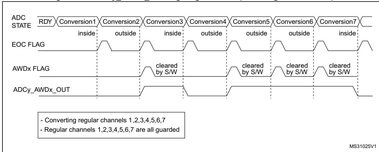
ADC STATE: RDY | Conversion1 (inside) | Conversion2 (outside) | Conversion3 (inside) | Conversion4 (outside) | Conversion5 (outside) | Conversion6 (outside) | Conversion7 (inside)
EOC FLAG: Pulses at the end of each conversion.
AWDx FLAG: Set by Conversion2, cleared by S/W after Conversion3. Set by Conversion4, cleared by S/W after Conversion5. Set by Conversion6, cleared by S/W after Conversion7.
ADCy_AWDx_OUT: High during Conversion2, low during Conversion3, high during Conversion4, low during Conversion5, high during Conversion6, low during Conversion7.
- - Converting regular channels 1,2,3,4,5,6,7
- - Regular channels 1,2,3,4,5,6,7 are all guarded
MS31025V1
Figure 184. ADCy_AWDx_OUT signal generation (AWDx flag not cleared by SW)
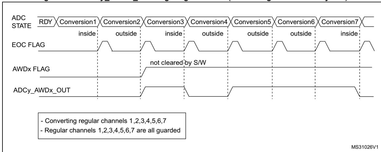
ADC STATE: RDY | Conversion1 (inside) | Conversion2 (outside) | Conversion3 (inside) | Conversion4 (outside) | Conversion5 (outside) | Conversion6 (outside) | Conversion7 (inside)
EOC FLAG: Pulses at the end of each conversion.
AWDx FLAG: Set by Conversion2, not cleared by S/W. Remains high for the rest of the sequence.
ADCy_AWDx_OUT: High during Conversion2, remains high through Conversion7.
- - Converting regular channels 1,2,3,4,5,6,7
- - Regular channels 1,2,3,4,5,6,7 are all guarded
MS31026V1
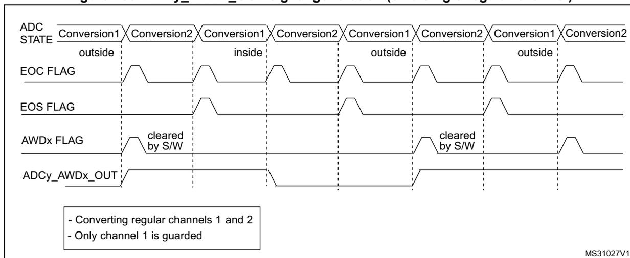
ADC STATE: Conversion1 (outside, inside, outside, outside), Conversion2
EOC FLAG: Pulses at the end of each conversion.
EOS FLAG: Pulses at the end of each sequence.
AWDx FLAG: Pulses when Conversion1 is outside, cleared by S/W.
ADC y _AWD x _OUT: High when Conversion1 is outside.
- - Converting regular channels 1 and 2
- - Only channel 1 is guarded
MS31027V1
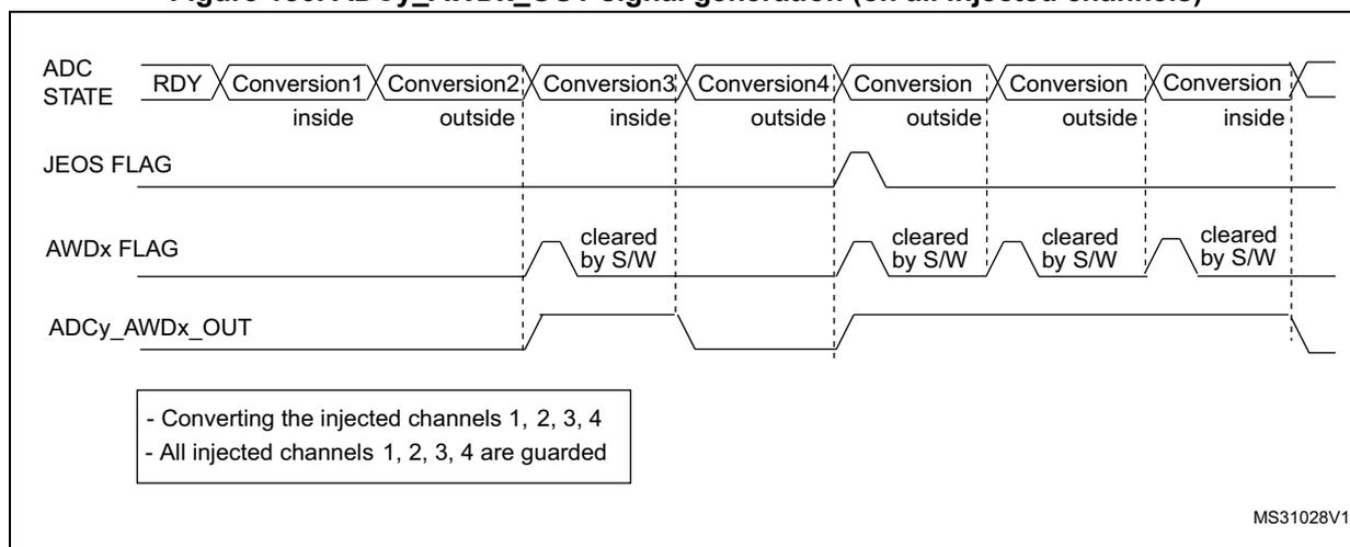
ADC STATE: RDY, Conversion1 (inside), Conversion2 (outside), Conversion3 (inside), Conversion4 (outside), Conversion (outside), Conversion (outside), Conversion (inside)
JEOS FLAG: Pulses at the end of the injected sequence.
AWDx FLAG: Pulses when any channel is outside, cleared by S/W.
ADC y _AWD x _OUT: High when any channel is outside.
- - Converting the injected channels 1, 2, 3, 4
- - All injected channels 1, 2, 3, 4 are guarded
MS31028V1
26.4.31 Oversampler
The oversampling unit performs data preprocessing to offload the CPU. It is able to handle multiple conversions and average them into a single data with increased data width, up to 26-bit (16-bit values and OSVR[9:0] = 1024).
It provides a result with the following form, where N and M can be adjusted:
It allows to perform by hardware the following functions: averaging, data rate reduction, SNR improvement, basic filtering.
The oversampling ratio N is defined using the OSVR[9:0] bits in the ADC_CFGR2 register, and can range from 2x to 1024x. The division coefficient M consists of a right bit shift up to 10 bits, and is defined using the OVSS[3:0] bits in the ADC_CFGR2 register.
The summation unit can yield a result up to 26 bits (1024 x 16-bit results), which can be left or right shifted. When right shifting is selected, it is rounded to the nearest value using the least significant bits left apart by the shifting, before being transferred into the ADC_DR data register.
The Table 187 gives a numerical example of the processing, from a raw 26-bit accumulated data to the final 16-bit result.
Figure 187. 16-bit result oversampling with 10-bits right shift and rounding
![Diagram showing four examples of 16-bit data processing with oversampling and right shifting. Each example shows a 32-bit register layout with bit positions 31, 23, 15, 7, and 0. The first example shows raw data D25..D0 with OVSS[3:0]=0. The second example shows data after right shifting and rounding with OVSS[3:0]=1010, resulting in D15..D0. The third example shows raw data 0x3FFFE258 with OVSS[3:0]=0. The fourth example shows data after right shifting and rounding with OVSS[3:0]=1010, resulting in 0xFFF9. Arrows indicate the 'Right shifting and rounding' process between the first and second, and third and fourth examples. MSv41028V2 is noted at the bottom right.](/RM0399-STM32H745-755-747-757/eb7c24e1db6cb8ef9691c1bb8f0e0213_img.jpg)
There are no changes for conversion timings in oversampled mode: the sample time is maintained equal during the whole oversampling sequence. A new data is provided every N conversions, with an equivalent delay equal to \( N \times T_{CONV} = N \times (t_{SAMPL} + t_{SAR}) \) . The flags are set as follow:
- • the end of the sampling phase (EOSMP) is set after each sampling phase
- • the end of conversion (EOC) occurs once every N conversions, when the oversampled result is available
- • the end of sequence (EOS) occurs once the sequence of oversampled data is completed (i.e. after N x sequence length conversions total)
Single ADC operating modes support when oversampling
In oversampling mode, most of the ADC operating modes are maintained:
- • Single or continuous mode conversions
- • ADC conversions start either by software or with triggers
- • ADC stop during a conversion (abort)
- • Data read via CPU or DMA with overrun detection
- • Low-power modes (AUTDLY)
- • Programmable resolution: in this case, the reduced conversion values (as per RES[2:0] bits in ADC_CFGR register) are accumulated, truncated, rounded and shifted in the same way as 16-bit conversions are
Note: The alignment mode is not available when working with oversampled data. The data are always provided right-aligned.
Analog watchdog
The analog watchdog functionality is maintained (AWDSGL and AWDEN bits), with the following difference:
- • the RES[2:0] bits are ignored, comparison is always done on using the full 26-bit values HTRx[25:0] and LTRx[25:0]
- • the comparison is performed on the oversampled accumulated value before shifting
Triggered mode
The averager can also be used for basic filtering purpose. Although not a very powerful filter (slow roll-off and limited stop band attenuation), it can be used as a notch filter to reject constant parasitic frequencies (typically coming from the mains or from a switched mode power supply). For this purpose, a specific discontinuous mode can be enabled with TROVS bit in ADC_CFGR2, to be able to have an oversampling frequency defined by a user and independent from the conversion time itself.
The Figure 188 below shows how conversions are started in response to triggers during discontinuous mode.
If the TROVS bit is set, the content of the DISCEN bit is ignored and considered as 1.
Figure 188. Triggered regular oversampling mode (TROVS bit = 1)
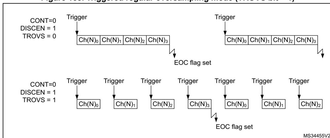
The diagram illustrates two scenarios for triggered regular oversampling mode (TROVS bit = 1).
Top scenario: CONT=0, DISCEN=1, TROVS=0. A single trigger starts a sequence of four conversions: Ch(N)0, Ch(N)1, Ch(N)2, and Ch(N)3. The EOC flag is set after the fourth conversion.
Bottom scenario: CONT=0, DISCEN=1, TROVS=1. Seven individual triggers start seven individual conversions: Ch(N)0, Ch(N)1, Ch(N)2, Ch(N)3, Ch(N)0, Ch(N)1, and Ch(N)2. The EOC flag is set after the seventh conversion.
The diagram shows the sequence of conversions and the trigger points for each scenario. The text MS34455V2 is visible in the bottom right corner of the diagram area.
Injected and regular sequencer management when oversampling
In oversampling mode, it is possible to have differentiated behavior for injected and regular sequencers. The oversampling can be enabled for both sequencers with some limitations if they have to be used simultaneously (this is related to a unique accumulation unit).
Oversampling regular channels only
The regular oversampling mode bit ROVSM defines how the regular oversampling sequence is resumed if it is interrupted by injected conversion:
- • in continued mode, the accumulation re-starts from the last valid data (prior to the conversion abort request due to the injected trigger). This ensures that oversampling is complete whatever the injection frequency (providing at least one regular conversion can be completed between triggers);
- • in resumed mode, the accumulation re-starts from 0 (previous conversions results are ignored). This mode allows to guarantee that all data used for oversampling were converted back-to-back within a single timeslot. Care must be taken to have a injection trigger period above the oversampling period length. If this condition is not respected, the oversampling cannot be complete and the regular sequencer is blocked.
The Figure 189 gives examples for a 4x oversampling ratio.
Figure 189. Regular oversampling modes (4x ratio)
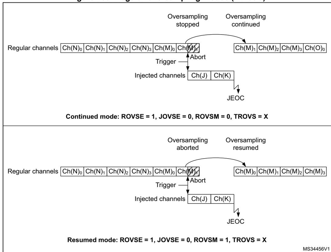
The diagram illustrates two scenarios for regular oversampling (4x ratio) when interrupted by injected channels.
Continued mode: ROVSE = 1, JOVSE = 0, ROVSM = 0, TROVS = X
In this mode, the regular oversampling sequence is continued after an injected conversion. The sequence of regular channels is Ch(N) 0 , Ch(N) 1 , Ch(N) 2 , Ch(N) 3 , Ch(M) 0 , Ch(M) 1 . A trigger occurs before Ch(M) 1 , causing an abort. Injected channels Ch(J) and Ch(K) are then converted, ending with JEOC. After the injection, the regular oversampling continues from Ch(M) 1 , followed by Ch(M) 2 , Ch(M) 3 , and Ch(O) 0 . The accumulation is continued from the last valid data (Ch(M) 1 ).
Resumed mode: ROVSE = 1, JOVSE = 0, ROVSM = 1, TROVS = X
In this mode, the regular oversampling sequence is aborted and then resumed from the beginning. The sequence of regular channels is Ch(N) 0 , Ch(N) 1 , Ch(N) 2 , Ch(N) 3 , Ch(M) 0 , Ch(M) 1 . A trigger occurs before Ch(M) 1 , causing an abort. Injected channels Ch(J) and Ch(K) are then converted, ending with JEOC. After the injection, the regular oversampling resumes from Ch(M) 0 , followed by Ch(M) 1 , Ch(M) 2 , and Ch(M) 3 . The accumulation is reset to 0.
MS34456V1
Oversampling Injected channels only
The Injected oversampling mode bit JOVSE enables oversampling solely for conversions in the injected sequencer.
Oversampling regular and Injected channels
It is possible to have both ROVSE and JOVSE bits set. In this case, the regular oversampling mode is forced to resumed mode (ROVSM bit ignored), as represented on Figure 190 below.
Figure 190. Regular and injected oversampling modes used simultaneously
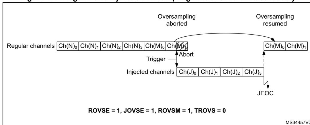
Regular channels: Ch(N) 0 | Ch(N) 1 | Ch(N) 2 | Ch(N) 3 | Ch(M) 0 | Ch(M) 1
Injected channels: Ch(J) 0 | Ch(J) 1 | Ch(J) 2 | Ch(J) 3
Events: Trigger, Abort, JEOC
States: Oversampling aborted, Oversampling resumed
Configuration: ROVSE = 1, JOVSE = 1, ROVSM = 1, TROVS = 0
MS34457V2
Triggered regular oversampling with injected conversions
It is possible to have triggered regular mode with injected conversions. In this case, the injected mode oversampling mode must be disabled, and the ROVSM bit is ignored (resumed mode is forced). The JOVSE bit must be reset. The behavior is represented on Figure 191 below.
Figure 191. Triggered regular oversampling with injection
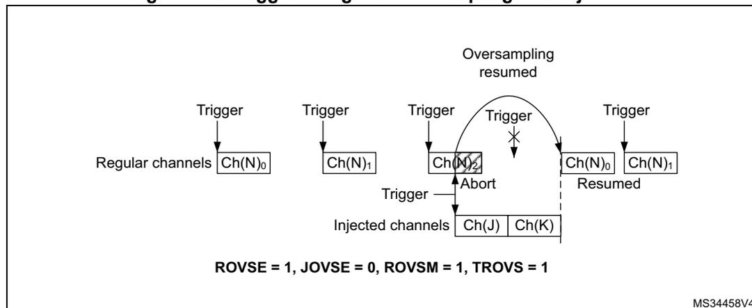
Regular channels: Ch(N) 0 | Ch(N) 1 | Ch(N) 2
Injected channels: Ch(J) | Ch(K)
Events: Trigger, Abort, Resumed
State: Oversampling resumed
Configuration: ROVSE = 1, JOVSE = 0, ROVSM = 1, TROVS = 1
MS34458V4
Auto-injected mode
It is possible to oversample auto-injected sequences and have all conversions results stored in registers to save a DMA resource. This mode is available only with both regular and injected oversampling active: JAUTO = 1, ROVSE = 1 and JOVSE = 1, other combinations are not supported. The ROVSM bit is ignored in auto-injected mode. The Figure 192 below shows how the conversions are sequenced.
Figure 192. Oversampling in auto-injected mode
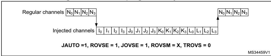
It is possible to have also the triggered mode enabled, using the TROVS bit. In this case, the ADC must be configured as following: JAUTO=1, DISCEN=0, JDISCEN=0, ROVSE=1, JOVSE=1 and TROVSE=1.
Dual ADC modes support when oversampling
It is possible to have oversampling enabled when working in dual ADC configuration, for the injected simultaneous mode and regular simultaneous mode. In this case, the two ADCs must be programmed with the very same settings (including oversampling).
All other dual ADC modes are not supported when either regular or injected oversampling is enabled (ROVSE = 1 or JOVSE = 1).
Combined modes summary
The Table 222 below summarizes all combinations, including modes not supported.
Table 222. Oversampler operating modes summary
| Regular Over-sampling ROVSE | Injected Over-sampling JOVSE | Oversampler mode ROVSM 0 = continued 1 = resumed | Triggered Regular mode TROVS | Comment |
|---|---|---|---|---|
| 1 | 0 | 0 | 0 | Regular continued mode |
| 1 | 0 | 0 | 1 | Not supported |
| 1 | 0 | 1 | 0 | Regular resumed mode |
| 1 | 0 | 1 | 1 | Triggered regular resumed mode |
| 1 | 1 | 0 | X | Not supported |
| 1 | 1 | 1 | 0 | Injected and regular resumed mode |
| 1 | 1 | 1 | 1 | Not supported |
| 0 | 1 | X | X | Injected oversampling |
26.4.32 Dual ADC modes
In devices with two ADCs or more, dual ADC modes can be used (see Figure 193 ):
- • ADC1 and ADC2 can be used together in dual mode (ADC1 is master)
In dual ADC mode the start of conversion is triggered alternately or simultaneously by the ADCx master to the ADC slave, depending on the mode selected by the bits DUAL[4:0] in the ADCx_CCR register.
Four possible modes are implemented:
- • Injected simultaneous mode
- • Regular simultaneous mode
- • Interleaved mode
- • Alternate trigger mode
It is also possible to use these modes combined in the following ways:
- • Injected simultaneous mode + Regular simultaneous mode
- • Regular simultaneous mode + Alternate trigger mode
- • Injected simultaneous mode + Interleaved mode
In dual ADC mode (when bits DUAL[4:0] in ADCx_CCR register are not equal to zero), the bits CONT, AUTDLY, DISCEN, DISCNUM[2:0], JDISCEN, JQM, JAUTO of the ADC_CFGR register are shared between the master and slave ADC: the bits in the slave ADC are always equal to the corresponding bits of the master ADC.
To start a conversion in dual mode, the user must program the bits EXTEN, EXTSEL, JEXTEN, JEXTSEL of the master ADC only, to configure a software or hardware trigger, and a regular or injected trigger. (the bits EXTEN[1:0] and JEXTEN[1:0] of the slave ADC are don't care).
In regular simultaneous or interleaved modes: once the user sets bit ADSTART or bit ADSTP of the master ADC, the corresponding bit of the slave ADC is also automatically set. However, bit ADSTART or bit ADSTP of the slave ADC is not necessary cleared at the same time as the master ADC bit.
In injected simultaneous or alternate trigger modes: once the user sets bit JADSTART or bit JADSTP of the master ADC, the corresponding bit of the slave ADC is also automatically set. However, bit JADSTART or bit JADSTP of the slave ADC is not necessary cleared at the same time as the master ADC bit.
In dual ADC mode, the converted data of the master and slave ADC can be read in parallel, by reading the ADC common data register (ADCx_CDR). The status bits can be also read in parallel by reading the dual-mode status register (ADCx_CSR).
Figure 193. Dual ADC block diagram (1)
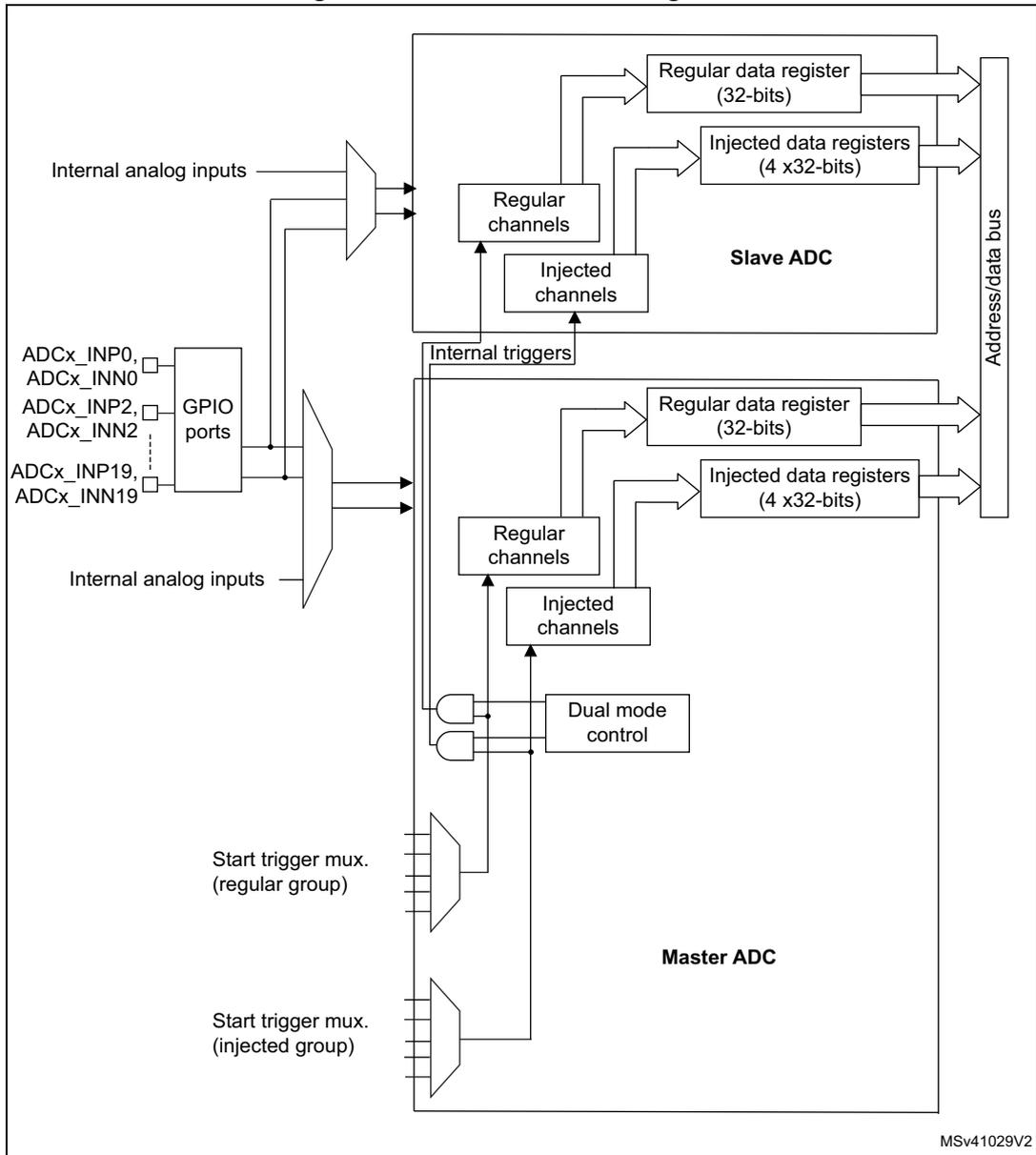
The diagram illustrates the internal architecture of a Dual ADC system. It consists of two main ADC units: a Master ADC and a Slave ADC. Both units are connected to a common Address/data bus on the right. The Master ADC (bottom) includes a 'Dual mode control' block, 'Start trigger mux. (regular group)', and 'Start trigger mux. (injected group)'. It has 'Regular channels' and 'Injected channels' leading to a 'Regular data register (32-bits)' and 'Injected data registers (4 x32-bits)'. The Slave ADC (top) has similar 'Regular channels' and 'Injected channels' leading to its own 'Regular data register (32-bits)' and 'Injected data registers (4 x32-bits)'. Both ADCs receive 'Internal triggers' from the Master ADC. Input signals include 'Internal analog inputs' and 'GPIO ports' (labeled with ADCx_INP0, ADCx_INN0, ADCx_INP2, ADCx_INN2, ..., ADCx_INP19, ADCx_INN19). The diagram is labeled MSv41029V2 in the bottom right corner.
- 1. External triggers also exist on slave ADC but are not shown for the purposes of this diagram.
- 2. The ADC common data register (ADCx_CDR) contains both the master and slave ADC regular converted data.
Injected simultaneous mode
This mode is selected by programming bits DUAL[4:0]=00101
This mode converts an injected group of channels. The external trigger source comes from the injected group multiplexer of the master ADC (selected by the JEXTSEL[4:0] bits in the ADC_JSQR register).
Note: Do not convert the same channel on the two ADCs (no overlapping sampling times for the two ADCs when converting the same channel).
In simultaneous mode, one must convert sequences with the same length and inside a sequence, the N-th conversion in master and slave must be configured with the same sampling time.
Regular conversions can be performed on one or all ADCs. In that case, they are independent of each other and are interrupted when an injected event occurs. They are resumed at the end of the injected conversion group.
- • At the end of injected sequence of conversion event (JEOS) on the master ADC, the converted data is stored into the master ADC_JDRy registers and a JEOS interrupt is generated (if enabled)
- • At the end of injected sequence of conversion event (JEOS) on the slave ADC, the converted data is stored into the slave ADC_JDRy registers and a JEOS interrupt is generated (if enabled)
- • If the duration of the master injected sequence is equal to the duration of the slave injected one (like in Figure 194), it is possible for the software to enable only one of the two JEOS interrupt (ex: master JEOS) and read both converted data (from master ADC_JDRy and slave ADC_JDRy registers).
Figure 194. Injected simultaneous mode on 4 channels: dual ADC mode

| MASTER ADC | CH1 | CH2 | CH3 | CH4 |
| SLAVE ADC | CH15 | CH14 | CH13 | CH12 |
Legend:
[Light Gray Box] Sampling
[White Box] Conversion
MS31900V1
If JDISCEN=1, each simultaneous conversion of the injected sequence requires an injected trigger event to occur.
This mode can be combined with AUTDLY mode:
- • Once a simultaneous injected sequence of conversions has ended, a new injected trigger event is accepted only if both JEOS bits of the master and the slave ADC have been cleared (delay phase). Any new injected trigger events occurring during the ongoing injected sequence and the associated delay phase are ignored.
- • Once a regular sequence of conversions of the master ADC has ended, a new regular trigger event of the master ADC is accepted only if the master data register (ADC_DR) has been read. Any new regular trigger events occurring for the master ADC during the ongoing regular sequence and the associated delay phases are ignored.
There is the same behavior for regular sequences occurring on the slave ADC.
Regular simultaneous mode with independent injected
This mode is selected by programming bits DUAL[4:0] = 00110.
This mode is performed on a regular group of channels. The external trigger source comes from the regular group multiplexer of the master ADC (selected by the EXTSEL[4:0] bits in the ADC_CFGR register). A simultaneous trigger is provided to the slave ADC.
In this mode, independent injected conversions are supported. An injection request (either on master or on the slave) aborts the current simultaneous conversions, which are re-started once the injected conversion is completed.
Note: Do not convert the same channel on the two ADCs (no overlapping sampling times for the two ADCs when converting the same channel).
In regular simultaneous mode, one must convert sequences with the same length and inside a sequence, the N-th conversion in master and slave must be configured with the same sampling time.
Software is notified by interrupts when it can read the data:
- • At the end of each conversion event (EOC) on the master ADC, a master EOC interrupt is generated (if EOCIE is enabled) and software can read the ADC_DR of the master ADC.
- • At the end of each conversion event (EOC) on the slave ADC, a slave EOC interrupt is generated (if EOCIE is enabled) and software can read the ADC_DR of the slave ADC.
- • If the duration of the master regular sequence is equal to the duration of the slave one (like in Figure 195 ), it is possible for the software to enable only one of the two EOC interrupt (ex: master EOC) and read both converted data from the Common Data register (ADCx_CDR).
It is also possible to read the regular data using the DMA. Two methods are possible:
- • Using two DMA channels (one for the master and one for the slave). In this case bits DAMDF[1:0] must be kept cleared.
- – Configure the DMA master ADC channel to read ADC_DR from the master. DMA requests are generated at each EOC event of the master ADC.
- – Configure the DMA slave ADC channel to read ADC_DR from the slave. DMA requests are generated at each EOC event of the slave ADC.
- • Configuring dual ADC mode data format DAMDF[1:0] bits, which leaves one DMA channel free for other uses:
- – Configure DAMDF[1:0]=0b10 or 0b11 (depending on resolution).
- – A single DMA channel is used (the one of the master). Configure the DMA master ADC channel to read the common ADC register (ADCx_CDR)
- – A single DMA request is generated each time both master and slave EOC events have occurred. At that time, the slave ADC converted data is available in the upper half-word of the ADCx_CDR 32-bit register and the master ADC converted data is available in the lower half-word of ADCx_CDR register.
- – both EOC flags are cleared when the DMA reads the ADCx_CDR register.
Note: When DAMDF[1:0]=0b10 or 0b11, the user must program the same number of conversions in the master's sequence as in the slave's sequence. Otherwise, the remaining conversions do not generate a DMA request.
Figure 195. Regular simultaneous mode on 16 channels: dual ADC mode
If DISCEN=1 then each “n” simultaneous conversions of the regular sequence require a regular trigger event to occur (“n” is defined by DISCNUM).
This mode can be combined with AUTDLY mode:
- Once a simultaneous conversion of the sequence has ended, the next conversion in the sequence is started only if the common data register, ADCx_CDR (or the regular data register of the master ADC) has been read (delay phase).
- Once a simultaneous regular sequence of conversions has ended, a new regular trigger event is accepted only if the common data register (ADCx_CDR) has been read (delay phase). Any new regular trigger events occurring during the ongoing regular sequence and the associated delay phases are ignored.
It is possible to use the DMA to handle data in regular simultaneous mode combined with AUTDLY mode, assuming that multiple-DMA mode is used: bits DAMDF must be set to 0b10 or 0b11.
When regular simultaneous mode is combined with AUTDLY mode, it is mandatory for the user to ensure that:
- The number of conversions in the master's sequence is equal to the number of conversions in the slave's.
- For each simultaneous conversions of the sequence, the length of the conversion of the slave ADC is inferior to the length of the conversion of the master ADC. Note that the length of the sequence depends on the number of channels to convert and the sampling time and the resolution of each channels.
Note: This combination of regular simultaneous mode and AUTDLY mode is restricted to the use case when only regular channels are programmed: it is forbidden to program injected channels in this combined mode.
Interleaved mode with independent injected
This mode is selected by programming bits DUAL[4:0] = 00111.
This mode can be started only on a regular group (usually one channel). The external trigger source comes from the regular channel multiplexer of the master ADC.
After an external trigger occurs:
- The master ADC starts immediately.
- The slave ADC starts after a delay of several-ADC clock cycles after the sampling phase of the master ADC has complete.
The minimum delay which separates 2 conversions in interleaved mode is configured in the DELAY bits in the ADCx_CCR register. This delay starts to count after the end of the sampling phase of the master conversion. This way, an ADC cannot start a conversion if the
complementary ADC is still sampling its input (only one ADC can sample the input signal at a given time).
- • The minimum possible DELAY is 1 to ensure that there is at least one cycle time between the opening of the analog switch of the master ADC sampling phase and the closing of the analog switch of the slave ADC sampling phase.
- • The maximum DELAY is equal to the number of cycles corresponding to the selected resolution. However the user must properly calculate this delay to ensure that an ADC does not start a conversion while the other ADC is still sampling its input.
If the CONT bit is set on both master and slave ADCs, the selected regular channels of both ADCs are continuously converted.
The software is notified by interrupts when it can read the data at the end of each conversion event (EOC) on the slave ADC. A slave and master EOC interrupts are generated (if EOCIE is enabled) and the software can read the ADC_DR of the slave/master ADC.
Note: It is possible to enable only the EOC interrupt of the slave and read the common data register (ADCx_CDR). But in this case, the user must ensure that the duration of the conversions are compatible to ensure that inside the sequence, a master conversion is always followed by a slave conversion before a new master conversion restarts. It is recommended to use the MDMA mode.
It is also possible to have the regular data transferred by DMA. In this case, individual DMA requests on each ADC cannot be used and it is mandatory to use the MDMA mode, as following:
- • Configure DAMDF[1:0]=0b10 or 0b11 (depending on resolution).
- • A single DMA channel is used (the one of the master). Configure the DMA master ADC channel to read the common ADC register (ADCx_CDR).
- • A single DMA request is generated each time both master and slave EOC events have occurred. At that time, the slave ADC converted data is available in the upper half-word of the ADCx_CDR 32-bit register and the master ADC converted data is available in the lower half-word of ADCx_CDR register.
- • Both EOC flags are cleared when the DMA reads the ADCx_CDR register.
Figure 196. Interleaved mode on 1 channel in continuous conversion mode: dual ADC mode
Figure 197. Interleaved mode on 1 channel in single conversion mode: dual ADC mode
If DISCEN=1, each “n” simultaneous conversions (“n” is defined by DISCNUM) of the regular sequence require a regular trigger event to occur.
In this mode, injected conversions are supported. When injection is done (either on master or on slave), both the master and the slave regular conversions are aborted and the sequence is re-started from the master (see Figure 198 below).
Figure 198. Interleaved conversion with injection
Alternate trigger mode
This mode is selected by programming bits DUAL[4:0] = 01001.
This mode can be started only on an injected group. The source of external trigger comes from the injected group multiplexer of the master ADC.
This mode is only possible when selecting hardware triggers: JEXTEN must not be 0x0.
Injected discontinuous mode disabled (JDISCEN=0 for both ADC)
- 1. When the 1st trigger occurs, all injected master ADC channels in the group are converted.
- 2. When the 2nd trigger occurs, all injected slave ADC channels in the group are converted.
- 3. And so on.
A JEOS interrupt, if enabled, is generated after all injected channels of the master ADC in the group have been converted.
A JEOS interrupt, if enabled, is generated after all injected channels of the slave ADC in the group have been converted.
JEOC interrupts, if enabled, can also be generated after each injected conversion.
If another external trigger occurs after all injected channels in the group have been converted then the alternate trigger process restarts by converting the injected channels of the master ADC in the group.
Figure 199. Alternate trigger: injected group of each ADC
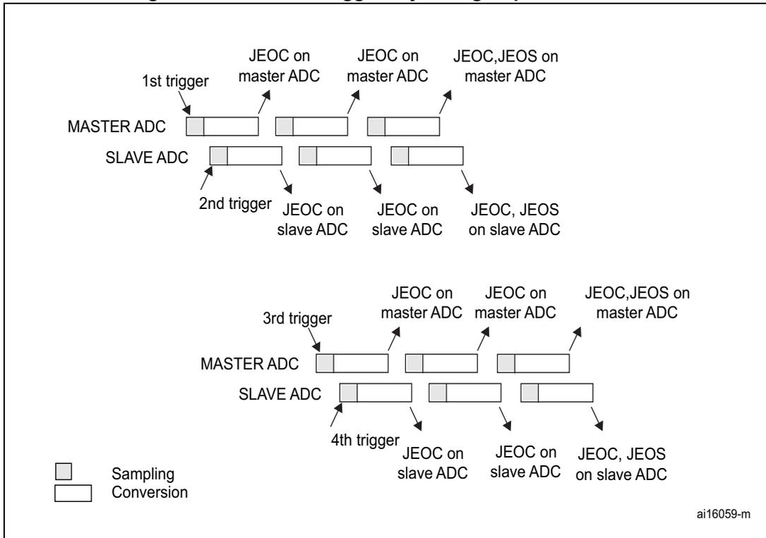
The diagram illustrates the timing of injected group conversions for a MASTER ADC and a SLAVE ADC under alternate triggering. The sequence starts with the 1st trigger for the MASTER ADC, followed by the 2nd trigger for the SLAVE ADC, then the 3rd trigger for the MASTER ADC, and finally the 4th trigger for the SLAVE ADC. Each trigger initiates a group of conversions. The diagram shows the progression of sampling and conversion phases for each group. Interrupts are generated at specific points: JEOC on master ADC after the first conversion of the first group, JEOC on master ADC after the second conversion of the first group, JEOC and JEOS on master ADC after the third conversion of the first group. Similarly, for the SLAVE ADC, JEOC is generated after the first and second conversions, and JEOC and JEOS are generated after the third conversion. The legend indicates that a shaded rectangle represents 'Sampling' and a white rectangle represents 'Conversion'.
Note: Regular conversions can be enabled on one or all ADCs. In this case the regular conversions are independent of each other. A regular conversion is interrupted when the ADC has to perform an injected conversion. It is resumed when the injected conversion is finished.
The time interval between 2 trigger events must be greater than or equal to 1 ADC clock period. The minimum time interval between 2 trigger events that start conversions on the same ADC is the same as in the single ADC mode.
Injected discontinuous mode enabled (JDISCEN=1 for both ADC)
If the injected discontinuous mode is enabled for both master and slave ADCs:
- • When the 1st trigger occurs, the first injected channel of the master ADC is converted.
- • When the 2nd trigger occurs, the first injected channel of the slave ADC is converted.
- • And so on.
A JEOS interrupt, if enabled, is generated after all injected channels of the master ADC in the group have been converted.
A JEOS interrupt, if enabled, is generated after all injected channels of the slave ADC in the group have been converted.
JEOC interrupts, if enabled, can also be generated after each injected conversions.
If another external trigger occurs after all injected channels in the group have been converted then the alternate trigger process restarts.
Figure 200. Alternate trigger: 4 injected channels (each ADC) in discontinuous mode
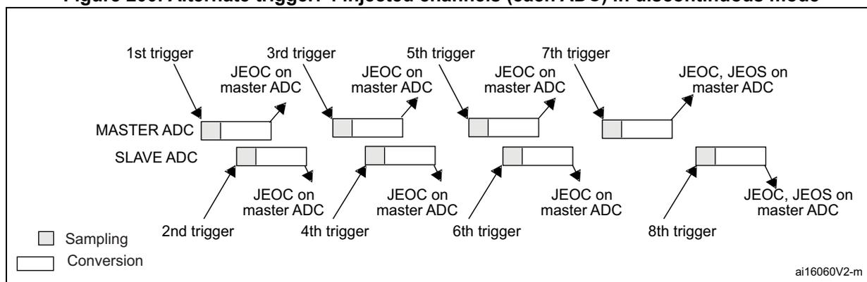
The diagram illustrates the timing and sequence of operations for two ADCs (Master and Slave) in injected discontinuous mode with 4 injected channels. The horizontal axis represents time, and the vertical axis distinguishes between the Master ADC and Slave ADC. Each ADC's state is shown as a sequence of 'Sampling' (shaded) and 'Conversion' (white) blocks. Triggers (1st through 8th) initiate the conversion of the first injected channel. JEOC (End of Conversion) and JEOS (End of Sequence) interrupts are generated when the respective sequences are complete. The Master ADC's sequence is triggered by odd-numbered triggers (1st, 3rd, 5th, 7th), while the Slave ADC's sequence is triggered by even-numbered triggers (2nd, 4th, 6th, 8th). The diagram shows that after the 4th injected channel of the Master ADC is converted, a JEOC interrupt is generated. Similarly, after the 4th injected channel of the Slave ADC is converted, a JEOS interrupt is generated. The 8th trigger restarts the Master ADC's sequence.
Legend:
[Shaded] Sampling
[White] Conversion
ai16060V2-m
Combined regular/injected simultaneous mode
This mode is selected by programming bits DUAL[4:0] = 00001.
It is possible to interrupt the simultaneous conversion of a regular group to start the simultaneous conversion of an injected group.
Note: The sequences must be converted with the same length, the N-th conversion in master and slave mode must be configured with the same sampling time inside a given sequence, or the interval between triggers has to be longer than the long conversion time of the 2 sequences. If the above conditions are not respected, the ADC with the shortest sequence may restart while the ADC with the longest sequence is completing the previous conversions.
Combined regular simultaneous + alternate trigger mode
This mode is selected by programming bits DUAL[4:0]=00010.
It is possible to interrupt the simultaneous conversion of a regular group to start the alternate trigger conversion of an injected group. Figure 201 shows the behavior of an alternate trigger interrupting a simultaneous regular conversion.
The injected alternate conversion is immediately started after the injected event. If a regular conversion is already running, in order to ensure synchronization after the injected
conversion, the regular conversion of all (master/slave) ADCs is stopped and resumed synchronously at the end of the injected conversion.
Note: The sequences must be converted with the same length, the N-th conversion in master and slave mode must be configured with the same sampling time inside a given sequence, or the interval between triggers has to be longer than the long conversion time of the 2 sequences. If the above conditions are not respected, the ADC with the shortest sequence may restart while the ADC with the longest sequence is completing the previous conversions.
Figure 201. Alternate + regular simultaneous
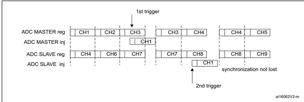
If a trigger occurs during an injected conversion that has interrupted a regular conversion, the alternate trigger is served. Figure 202 shows the behavior in this case (note that the 6th trigger is ignored because the associated alternate conversion is not complete).
Figure 202. Case of trigger occurring during injected conversion
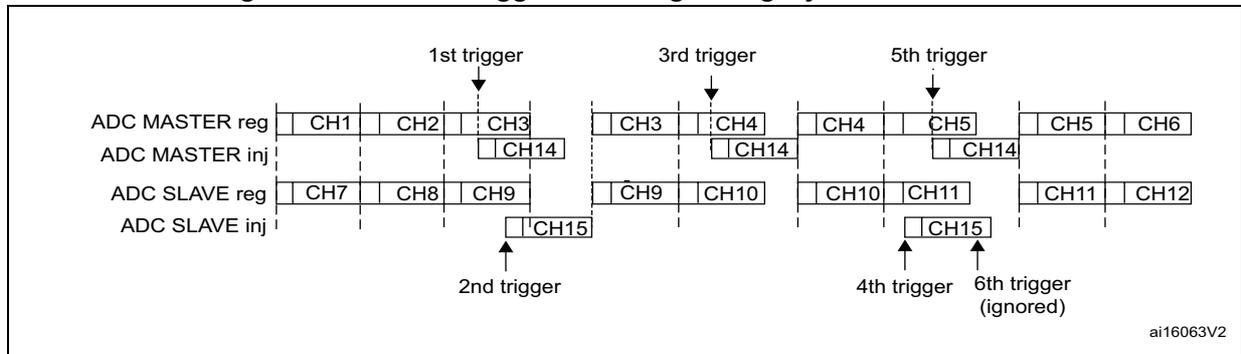
Combined injected simultaneous plus interleaved
This mode is selected by programming bits DUAL[4:0]=00011.
It is possible to interrupt an interleaved conversion with a simultaneous injected event.
In this case the interleaved conversion is interrupted immediately and the simultaneous injected conversion starts. At the end of the injected sequence the interleaved conversion is resumed. When the interleaved regular conversion resumes, the first regular conversion which is performed is always the master's one. Figure 203, Figure 204 and Figure 205 show the behavior using an example.
Caution: In this mode, it is mandatory to use the Common Data Register to read the regular data with a single read access. On the contrary, master-slave data coherency is not guaranteed.
Figure 203. Interleaved single channel CH0 with injected sequence CH11, CH12
Figure 204. Two Interleaved channels (CH1, CH2) with injected sequence CH11, CH12 - case 1: Master interrupted first
Figure 205. Two Interleaved channels (CH1, CH2) with injected sequence CH11, CH12 - case 2: Slave interrupted first
DMA requests in dual ADC mode
In all dual ADC modes, it is possible to use two DMA channels (one for the master, one for the slave) to transfer the data, like in single mode (refer to Figure 206: DMA Requests in regular simultaneous mode when DAMDF=0b00 ).
Figure 206. DMA Requests in regular simultaneous mode when DAMDF=0b00
Configuration where each sequence contains only one conversion
MSV31032V2
In simultaneous regular and interleaved modes, it is also possible to save one DMA channel and transfer both data using a single DMA channel. For this DAMDF bits must be configured in the ADCx_CCR register:
- • DAMDF=0b10, 32-bit format: A single DMA request is generated alternatively when either the master or slave EOC events have occurred. At that time, the data items are alternatively available in the ADCx_CDR2 32-bit register. This mode is used in interleaved mode and in regular simultaneous mode when resolution is above 16-bit.
Example:
Interleaved dual mode: a DMA request is generated each time a new 32-bit data is available:
1st DMA request: ADCx_CDR2[31:0] = MST_ADC_DR[31:0]
2nd DMA request: ADCx_CDR2[31:0] = SLV_ADC_DR[31:0]
- • DAMDF=0b10, 16-bit format: A single DMA request is generated each time both master and slave EOC events have occurred. At that time, two data items are available and the 32-bit register ADCx_CDR contains the two half-words representing two ADC-
converted data items. The slave ADC data take the upper half-word and the master ADC data take the lower half-word.
This mode is used in interleaved mode and in regular simultaneous mode when resolution is ranging from 10 to 16-bit. Any value above 16-bit in the master or the slave converter is truncated to the least 16 significant bits.
Example:
Interleaved dual mode: a DMA request is generated each time 2 data items are available:
1st DMA request: \( ADCx\_CDR[31:0] = SLV\_ADC\_DR[15:0] \mid MST\_ADC\_DR[15:0] \)
2nd DMA request: \( ADCx\_CDR[31:0] = SLV\_ADC\_DR[15:0] \mid MST\_ADC\_DR[15:0] \)
Figure 207. DMA requests in regular simultaneous mode when DAMDF=0b10
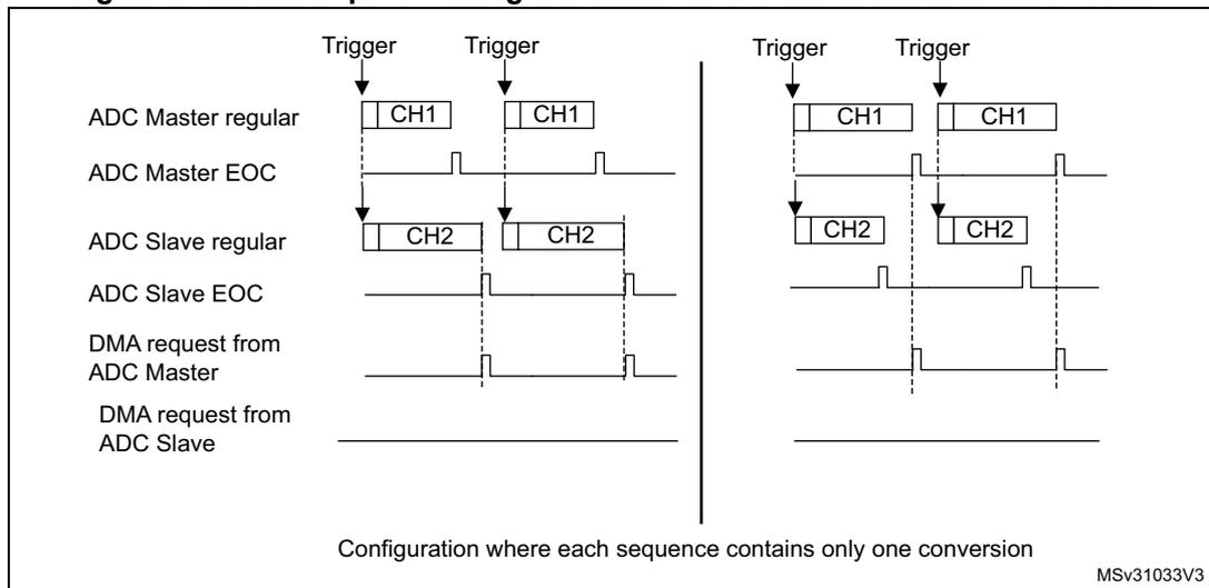
Configuration where each sequence contains only one conversion
MSV31033V3
Figure 208. DMA requests in interleaved mode when DAMDF=0b10
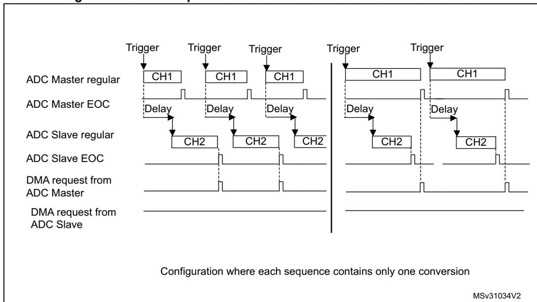
Configuration where each sequence contains only one conversion
MSV31034V2
Note: When using multiple-ADC mode, the user must take care to configure properly the duration of the master and slave conversions so that a DMA request is generated and served for reading both data (master + slave) before a new conversion is available.
- • DAMDF=0b11: This mode is similar to the DAMDF=0b10. The only differences are that on each DMA request (two data items are available), two bytes representing two ADC converted data items are transferred as a half-word.
This mode is used in interleaved and regular simultaneous mode when the result is 8-bit. A new DMA request is issued when 4 new 8-bit values are available.
Example:
Interleaved dual mode: a DMA request is generated each time 4 data items are available (t0, t1,... are corresponding to the consecutive sampling instants)
1st DMA request:
ADCx_CDR[7:0] = MST_ADC_DR[7:0]t0
ADCx_CDR[15:8] = SLV_ADC_DR[7:0]t0
ADCx_CDR[23:16] = MST_ADC_DR[7:0]t1
ADCx_CDR[31:24] = SLV_ADC_DR[7:0]t1
2nd DMA request:
ADCx_CDR[7:0] = MST_ADC_DR[7:0]t2
ADCx_CDR[15:8] = SLV_ADC_DR[7:0]t2
ADCx_CDR[23:16] = MST_ADC_DR[7:0]t3
ADCx_CDR[31:24] = SLV_ADC_DR[7:0]t3
Overrun detection
In dual ADC mode (when DUAL[4:0] is not equal to b00000), if an overrun is detected on one of the ADCs, the DMA requests are no longer issued to ensure that all the data transferred to the RAM are valid (this behavior occurs whatever the DAMDF configuration). It may happen that the EOC bit corresponding to one ADC remains set because the data register of this ADC contains valid data.
DMA one shot mode/ DMA circular mode when multiple-ADC mode is selected
When DAMDF mode is selected (0b10 or 0b11), bit DMNGT[1:0]=0b10 in the master ADC's ADCx_CCR register must also be configured to select between DMA one shot mode and circular mode, as explained in section Section : Managing conversions using the DMA .
Stopping the conversions in dual ADC modes
The user must set the control bits ADSTP/JADSTP of the master ADC to stop the conversions of both ADC in dual ADC mode. The other ADSTP control bit of the slave ADC has no effect in dual ADC mode.
Once both ADC are effectively stopped, the bits ADSTART/JADSTART of the master and slave ADCs are both cleared by hardware.
DFSDM mode in dual ADC mode interleaved mode
In dual ADC interleaved modes, the ADC conversion results can be transferred directly to the Digital Filter for Sigma Delta Modulators (DFSDM).
This mode is enabled by setting the bits DMNGT[1:0] = 0b10 in the master ADC's ADC_CFGR register.
The ADC transfers alternatively the 16 least significant bits of the regular data register from the master and the slave converter to a single channel of the DFSDM.
The data format must be 16-bit signed:
ADC_DR[31:16] = 0x0000
ADC_DR[15] = sign
ADC_DR[14:0] = data
Any value above 16-bit signed format in any converter is truncated.
DFSDM mode in dual ADC simultaneous mode
The dual mode is not required to use DFSDM in dual ADC simultaneous mode since conversion data are treated by each individual channel. Single mode with same trigger source results in simultaneous conversion with DFSDM interface.
26.4.33 Temperature sensor
The temperature sensor can measure the junction temperature ( \( T_J \) ) of the device in the \( -40 \) to \( 125 \) °C temperature range.
The temperature sensor is internally connected to an ADC internal channel which is used to convert the sensor's output voltage to a digital value (refer to Table ADC interconnection in Section 26.4.2: ADC pins and internal signals ). The sampling time for the temperature sensor's analog pin must be greater than the stabilization time specified in the product datasheet.
When not in use, the sensor can be put in power-down mode.
Figure 209 shows the block diagram of the temperature sensor.
Figure 209. Temperature sensor channel block diagram
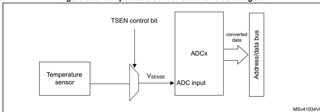
graph LR
    TS[Temperature sensor] --> MUX{ }
    TSEN[TSEN control bit] --> MUX
    MUX -- VSENSE --> ADC[ADCx ADC input]
    ADC -- converted data --> BUS[Address/data bus]
Note: The TSEN bit must be set to enable the conversion of the corresponding ADC internal channel (temperature sensor, \( V_{SENSE} \) ).
Reading the temperature
To use the sensor:
- 1. Select the ADC input channels (with the appropriate sampling time).
- 2. Program with the appropriate sampling time (refer to electrical characteristics section of the device datasheet).
- 3. Set the TSEN bit in the ADCx_CCR register to wake up the temperature sensor from power-down mode.
- 4. Start the ADC conversion.
- 5. Read the resulting \( V_{SENSE} \) data in the ADC data register.
- 6. Calculate the actual temperature using the following formula:
Where:
- • TS_CAL2 is the temperature sensor calibration value acquired at TS_CAL2_TEMP
- • TS_CAL1 is the temperature sensor calibration value acquired at TS_CAL1_TEMP
- • TS_DATA is the actual temperature sensor output value converted by ADC
- Refer to the device datasheet for more information about TS_CAL1 and TS_CAL2 calibration points.
Note: The sensor has a startup time after waking from power-down mode before it can output \( V_{SENSE} \) at the correct level. The ADC also has a startup time after power-on, so to minimize the delay, the ADEN and SENSEEN bits should be set at the same time.
26.4.34 \( V_{BAT} \) supply monitoring
The VBATEN bit of the ADCx_CCR register is used to switch to the battery voltage. As the \( V_{BAT} \) voltage could be higher than \( V_{DDA} \) , to ensure the correct operation of the ADC, the \( V_{BAT} \) pin is internally connected to a bridge divider by 4. This bridge is automatically enabled when VBATEN is set, to connect \( V_{BAT}/4 \) to an ADC input channel (refer to Table ADC interconnection in Section 26.4.2: ADC pins and internal signals ).
As a consequence, the converted digital value is one fourth of the \( V_{BAT} \) voltage. To prevent any unwanted consumption on the battery, it is recommended to enable the bridge divider only when needed, for ADC conversion.
Refer to the electrical characteristics of the device datasheet for the sampling time value to be applied when converting the \( V_{BAT}/4 \) voltage.
Figure 210 shows the block diagram of the \( V_{BAT} \) sensing feature.
Figure 210.\( V_{BAT} \) channel block diagram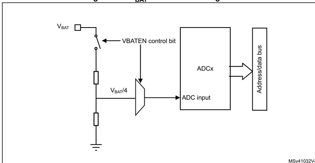
The diagram shows a switch connected to \( V_{BAT} \) at the top. The switch is controlled by the \( V_{BATEN} \) control bit. The output of the switch is connected to a voltage divider consisting of two resistors in series, with the midpoint labeled \( V_{BAT}/4 \) . This midpoint is connected to a multiplexer. The output of the multiplexer is connected to the \( ADC \) input of the \( ADCx \) block. The \( ADCx \) block is connected to an Address/data bus. The bottom of the voltage divider is connected to ground. The diagram is labeled MSv41032V4 in the bottom right corner.
Note: The \( V_{BATEN} \) bit in \( ADCx\_CCR \) must be configured to enable the conversion of the corresponding ADC internal channel.
26.4.35 Monitoring the internal voltage reference
The internal voltage reference can be monitored to have a reference point for evaluating the ADC \( V_{REF+} \) voltage level.
The internal voltage reference is internally connected to an ADC input channel (refer to Table ADC interconnection in Section 26.4.2: ADC pins and internal signals ).
The sampling time for this channel must be greater than the stabilization time specified in the product datasheet.
Figure 210 shows the block diagram of the \( V_{REFINT} \) sensing feature.
Figure 211.\( V_{REFINT} \) channel block diagram
The diagram shows an Internal power block connected to a multiplexer. The output of the internal power block is labeled \( V_{REFINT} \) . The multiplexer is controlled by the \( V_{REFEN} \) control bit. The output of the multiplexer is connected to the \( ADC \) input of the \( ADCx \) block. The diagram is labeled MSv41033V5 in the bottom right corner.
Note: The \( V_{REFEN} \) bit of the \( ADCx\_CCR \) register must be configured to enable the conversion of the corresponding ADC internal channel ( \( V_{REFINT} \) ).
Calculating the actual \( V_{DDA} \) voltage using the internal reference voltage
The power supply voltage applied to the device may be subject to variations or not precisely known. When \( V_{DDA} \) is connected to \( V_{REF+} \) , it is possible to compute the actual \( V_{DDA} \) voltage using the embedded internal reference voltage ( \( V_{REFINT} \) ). \( V_{REFINT} \) and its calibration data acquired by the ADC during the manufacturing process at \( V_{DDA} = 3.3\text{ V} \) can be used to evaluate the actual \( V_{DDA} \) voltage level.
The following formula gives the actual \( V_{DDA} \) voltage supplying the device:
Where:
- • \( VREFINT\_CAL \) is the \( VREFINT \) calibration value
- • \( VREFINT\_DATA \) is the actual \( VREFINT \) output value converted by ADC
Converting a supply-relative ADC measurement to an absolute voltage value
The ADC is designed to deliver a digital value corresponding to the ratio between \( V_{REF+} \) and the voltage applied on the converted channel.
For most applications \( V_{DDA} \) value is unknown and ADC converted values are right-aligned. In this case, it is necessary to convert this ratio into a voltage independent from \( V_{DDA} \) :
By replacing \( V_{REF+} \) by the formula provided above, the absolute voltage value is given by the following formula
For applications where \( V_{DDA} \) is known and ADC converted values are right-aligned, the absolute voltage value can be obtained by using the following formula:
Where:
- – \( VREFINT\_CAL \) is the \( VREFINT \) calibration value
- – \( ADC\_DATA \) is the value measured by the ADC on channel x (right-aligned)
- – \( VREFINT\_DATA \) is the actual \( VREFINT \) output value converted by the ADC
- – \( FULL\_SCALE \) is the maximum digital value of the ADC output. For example with 16-bit resolution, it is \( 2^{16} - 1 = 65535 \) or with 8-bit resolution, \( 2^8 - 1 = 255 \) .
Note: If ADC measurements are done using an output format other than 16-bit right-aligned, all the parameters must first be converted to a compatible format before the calculation is done.
26.5 ADC interrupts
For each ADC, an interrupt can be generated:
- • After ADC power-up, when the ADC is ready (flag ADRDY)
- • On the end of any conversion for regular groups (flag EOC)
- • On the end of a sequence of conversion for regular groups (flag EOS)
- • On the end of any conversion for injected groups (flag JEOC)
- • On the end of a sequence of conversion for injected groups (flag JEOS)
- • When an analog watchdog detection occurs (flag AWD1, AWD2 and AWD3)
- • When the end of sampling phase occurs (flag EOSMP)
- • When the data overrun occurs (OVR flag)
- • When the injected sequence context queue overflows (flag JQOVF)
Separate interrupt enable bits are available for flexibility.
Table 223. ADC interrupts per each ADC
| Interrupt event | Event flag | Enable control bit |
|---|---|---|
| ADC ready | ADRDY | ADRDYIE |
| End of conversion of a regular group | EOC | EOCIE |
| End of sequence of conversions of a regular group | EOS | EOSIE |
| End of conversion of a injected group | JEOC | JEOCIE |
| End of sequence of conversions of an injected group | JEOS | JEOSIE |
| Analog watchdog 1 status bit is set | AWD1 | AWD1IE |
| Analog watchdog 2 status bit is set | AWD2 | AWD2IE |
| Analog watchdog 3 status bit is set | AWD3 | AWD3IE |
| End of sampling phase | EOSMP | EOSMPIE |
| Overrun | OVR | OVRIE |
| Injected context queue overflows | JQOVF | JQOVFIE |
26.6 ADC registers (for each ADC)
Refer to Section 1.2 on page 106 for a list of abbreviations used in register descriptions.
26.6.1 ADC interrupt and status register (ADC_ISR)
Address offset: 0x00
Reset value: 0x0000 0000
| 31 | 30 | 29 | 28 | 27 | 26 | 25 | 24 | 23 | 22 | 21 | 20 | 19 | 18 | 17 | 16 |
|---|---|---|---|---|---|---|---|---|---|---|---|---|---|---|---|
| Res. | Res. | Res. | Res. | Res. | Res. | Res. | Res. | Res. | Res. | Res. | Res. | Res. | Res. | Res. | Res. |
| 15 | 14 | 13 | 12 | 11 | 10 | 9 | 8 | 7 | 6 | 5 | 4 | 3 | 2 | 1 | 0 |
| Res. | Res. | Res. | LDOR DY | Res. | JQOVF | AWD3 | AWD2 | AWD1 | JEOS | JEOC | OVR | EOS | EOC | EOSMP | ADRDY |
| r | rc_w1 | rc_w1 | rc_w1 | rc_w1 | rc_w1 | rc_w1 | rc_w1 | rc_w1 | rc_w1 | rc_w1 | rc_w1 |
Bits 31:13 Reserved, must be kept at reset value.
Bit 12 LDORDY: ADC LDO output voltage ready bit
This bit is set and cleared by hardware. It indicates that the ADC internal LDO output is ready and that the ADC can be enabled or calibrated.
0: ADC LDO voltage regulator disabled
1: ADC LDO voltage regulator enabled
Note: Refer to Section 26.3: ADC implementation for the availability of the LDO regulator.
Bit 11 Reserved, must be kept at reset value.
Bit 10 JQOVF: Injected context queue overflow
This bit is set by hardware when an Overflow of the Injected Queue of Context occurs. It is cleared by software writing 1 to it. Refer to Section 26.4.22: Queue of context for injected conversions for more information.
0: No injected context queue overflow occurred (or the flag event was already acknowledged and cleared by software)
1: Injected context queue overflow has occurred
Bit 9 AWD3: Analog watchdog 3 flag
This bit is set by hardware when the converted voltage crosses the values programmed in the fields LT3[7:0] and HT3[7:0] of ADC_TR3 register. It is cleared by software writing 1 to it.
0: No analog watchdog 3 event occurred (or the flag event was already acknowledged and cleared by software)
1: Analog watchdog 3 event occurred
Bit 8 AWD2: Analog watchdog 2 flag
This bit is set by hardware when the converted voltage crosses the values programmed in the fields LT2[7:0] and HT2[7:0] of ADC_TR2 register. It is cleared by software writing 1 to it.
0: No analog watchdog 2 event occurred (or the flag event was already acknowledged and cleared by software)
1: Analog watchdog 2 event occurred
Bit 7 AWD1: Analog watchdog 1 flagThis bit is set by hardware when the converted voltage crosses the values programmed in the fields LT1[11:0] and HT1[11:0] of ADC_TR1 register. It is cleared by software, writing 1 to it.
0: No analog watchdog 1 event occurred (or the flag event was already acknowledged and cleared by software)
1: Analog watchdog 1 event occurred
Bit 6 JEOS: Injected channel end of sequence flagThis bit is set by hardware at the end of the conversions of all injected channels in the group. It is cleared by software writing 1 to it.
0: Injected conversion sequence not complete (or the flag event was already acknowledged and cleared by software)
1: Injected conversions complete
Bit 5 JEOC: Injected channel end of conversion flagThis bit is set by hardware at the end of each injected conversion of a channel when a new data is available in the corresponding ADC_JDRy register. It is cleared by software writing 1 to it or by reading the corresponding ADC_JDRy register
0: Injected channel conversion not complete (or the flag event was already acknowledged and cleared by software)
1: Injected channel conversion complete
Bit 4 OVR: ADC overrunThis bit is set by hardware when an overrun occurs on a regular channel, meaning that a new conversion has completed while the EOC flag was already set. It is cleared by software writing 1 to it.
0: No overrun occurred (or the flag event was already acknowledged and cleared by software)
1: Overrun has occurred
Bit 3 EOS: End of regular sequence flagThis bit is set by hardware at the end of the conversions of a regular sequence of channels. It is cleared by software writing 1 to it.
0: Regular Conversions sequence not complete (or the flag event was already acknowledged and cleared by software)
1: Regular Conversions sequence complete
Bit 2 EOC: End of conversion flagThis bit is set by hardware at the end of each regular conversion of a channel when a new data is available in the ADC_DR register. It is cleared by software writing 1 to it or by reading the ADC_DR register
0: Regular channel conversion not complete (or the flag event was already acknowledged and cleared by software)
1: Regular channel conversion complete
Bit 1 EOSMP: End of sampling flagThis bit is set by hardware during the conversion of any channel (only for regular channels), at the end of the sampling phase.
0: not at the end of the sampling phase (or the flag event was already acknowledged and cleared by software)
1: End of sampling phase reached
Bit 0 ADRDY: ADC readyThis bit is set by hardware after the ADC has been enabled (bit ADEN=1) and when the ADC reaches a state where it is ready to accept conversion requests.
It is cleared by software writing 1 to it.
0: ADC not yet ready to start conversion (or the flag event was already acknowledged and cleared by software)
1: ADC is ready to start conversion
26.6.2 ADC interrupt enable register (ADC_IER)
Address offset: 0x04
Reset value: 0x0000 0000
| 31 | 30 | 29 | 28 | 27 | 26 | 25 | 24 | 23 | 22 | 21 | 20 | 19 | 18 | 17 | 16 |
|---|---|---|---|---|---|---|---|---|---|---|---|---|---|---|---|
| Res. | Res. | Res. | Res. | Res. | Res. | Res. | Res. | Res. | Res. | Res. | Res. | Res. | Res. | Res. | Res. |
| 15 | 14 | 13 | 12 | 11 | 10 | 9 | 8 | 7 | 6 | 5 | 4 | 3 | 2 | 1 | 0 |
| Res. | Res. | Res. | Res. | Res. | JQOVF IE | AWD3 IE | AWD2 IE | AWD1 IE | JEOSIE | JEOCIE | OVR IE | EOSIE | EOCIE | EOSMP IE | ADRDY IE |
| rw | rw | rw | rw | rw | rw | rw | rw | rw | rw | rw |
Bits 31:11 Reserved, must be kept at reset value.
Bit 10 JQOVFIE: Injected context queue overflow interrupt enable
This bit is set and cleared by software to enable/disable the Injected Context Queue Overflow interrupt.
0: Injected Context Queue Overflow interrupt disabled
1: Injected Context Queue Overflow interrupt enabled. An interrupt is generated when the JQOVF bit is set.
Note: The software is allowed to write this bit only when JADSTART=0 (which ensures that no injected conversion is ongoing).
Bit 9 AWD3IE: Analog watchdog 3 interrupt enable
This bit is set and cleared by software to enable/disable the analog watchdog 2 interrupt.
0: Analog watchdog 3 interrupt disabled
1: Analog watchdog 3 interrupt enabled
Note: The software is allowed to write this bit only when ADSTART=0 and JADSTART=0 (which ensures that no conversion is ongoing).
Bit 8 AWD2IE: Analog watchdog 2 interrupt enable
This bit is set and cleared by software to enable/disable the analog watchdog 2 interrupt.
0: Analog watchdog 2 interrupt disabled
1: Analog watchdog 2 interrupt enabled
Note: The software is allowed to write this bit only when ADSTART=0 and JADSTART=0 (which ensures that no conversion is ongoing).
Bit 7 AWD1IE: Analog watchdog 1 interrupt enable
This bit is set and cleared by software to enable/disable the analog watchdog 1 interrupt.
0: Analog watchdog 1 interrupt disabled
1: Analog watchdog 1 interrupt enabled
Note: The software is allowed to write this bit only when ADSTART=0 and JADSTART=0 (which ensures that no conversion is ongoing).
Bit 6 JEOSIE: End of injected sequence of conversions interrupt enable
This bit is set and cleared by software to enable/disable the end of injected sequence of conversions interrupt.
0: JEOS interrupt disabled
1: JEOS interrupt enabled. An interrupt is generated when the JEOS bit is set.
Note: The software is allowed to write this bit only when JADSTART=0 (which ensures that no injected conversion is ongoing).
Bit 5 JEOCIE: End of injected conversion interrupt enableThis bit is set and cleared by software to enable/disable the end of an injected conversion interrupt.
0: JEOC interrupt disabled.
1: JEOC interrupt enabled. An interrupt is generated when the JEOC bit is set.
Note: The software is allowed to write this bit only when JADSTART is cleared to 0 (no injected conversion is ongoing).
Bit 4 OVRIE: Overrun interrupt enableThis bit is set and cleared by software to enable/disable the Overrun interrupt of a regular conversion.
0: Overrun interrupt disabled
1: Overrun interrupt enabled. An interrupt is generated when the OVR bit is set.
Note: The software is allowed to write this bit only when ADSTART=0 (which ensures that no regular conversion is ongoing).
Bit 3 EOSIE: End of regular sequence of conversions interrupt enableThis bit is set and cleared by software to enable/disable the end of regular sequence of conversions interrupt.
0: EOS interrupt disabled
1: EOS interrupt enabled. An interrupt is generated when the EOS bit is set.
Note: The software is allowed to write this bit only when ADSTART=0 (which ensures that no regular conversion is ongoing).
Bit 2 EOCIE: End of regular conversion interrupt enableThis bit is set and cleared by software to enable/disable the end of a regular conversion interrupt.
0: EOC interrupt disabled.
1: EOC interrupt enabled. An interrupt is generated when the EOC bit is set.
Note: The software is allowed to write this bit only when ADSTART=0 (which ensures that no regular conversion is ongoing).
Bit 1 EOSMPIE: End of sampling flag interrupt enable for regular conversionsThis bit is set and cleared by software to enable/disable the end of the sampling phase interrupt for regular conversions.
0: EOSMP interrupt disabled.
1: EOSMP interrupt enabled. An interrupt is generated when the EOSMP bit is set.
Note: The software is allowed to write this bit only when ADSTART=0 (which ensures that no regular conversion is ongoing).
Bit 0 ADRDYIE: ADC ready interrupt enableThis bit is set and cleared by software to enable/disable the ADC Ready interrupt.
0: ADRDY interrupt disabled
1: ADRDY interrupt enabled. An interrupt is generated when the ADRDY bit is set.
Note: The software is allowed to write this bit only when ADSTART=0 and JADSTART=0 (which ensures that no conversion is ongoing).
26.6.3 ADC control register (ADC_CR)
Address offset: 0x08
Reset value: 0x2000 0000
| 31 | 30 | 29 | 28 | 27 | 26 | 25 | 24 | 23 | 22 | 21 | 20 | 19 | 18 | 17 | 16 |
|---|---|---|---|---|---|---|---|---|---|---|---|---|---|---|---|
| ADCAL L | ADCAL LDIF | DEEP PWD | ADVREG EN | LINCA LRDY W6 | LINCA LRDY W5 | LINCA LRDY W4 | LINCAL RDYW3 | LINCAL RDYW2 | LINCAL RDYW1 | Res. | Res. | Res. | Res. | Res. | ADCAL LIN |
| rs | rw | rw | rw | rw | rw | rw | rw | rw | rw | rw | |||||
| 15 | 14 | 13 | 12 | 11 | 10 | 9 | 8 | 7 | 6 | 5 | 4 | 3 | 2 | 1 | 0 |
| Res. | Res. | Res. | Res. | Res. | Res. | BOOST[1:0] | Res. | Res. | JADSTP | ADSTP | JADST ART | ADSTA RT | ADDIS | ADEN | |
| rw | rw | rs | rs | rs | rs | rs | rs | ||||||||
Bit 31 ADCAL: ADC calibration
This bit is set by software to start the calibration of the ADC. Program first the bit ADCALDIF to determine if this calibration applies for single-ended or differential inputs mode.
It is cleared by hardware after calibration is complete.
0: Calibration complete
1: Write 1 to calibrate the ADC. Read at 1 means that a calibration in progress.
Note: The software is allowed to launch a calibration by setting ADCAL only when ADEN=0.
The software is allowed to update the calibration factor by writing ADC_CALFACT only when ADEN=1 and ADSTART=0 and JADSTART=0 (ADC enabled and no conversion is ongoing)
Bit 30 ADCALDIF: Differential mode for calibration
This bit is set and cleared by software to configure the single-ended or differential inputs mode for the calibration.
0: Writing ADCAL launches a calibration in single-ended inputs mode.
1: Writing ADCAL launches a calibration in differential inputs mode.
Note: The software is allowed to write this bit only when the ADC is disabled and is not calibrating (ADCAL=0, JADSTART=0, JADSTP=0, ADSTART=0, ADSTP=0, ADDIS=0 and ADEN=0).
Bit 29 DEEPPWD: Deep-power-down enable
This bit is set and cleared by software to put the ADC in deep-power-down mode.
0: ADC not in deep-power down
1: ADC in deep-power-down (default reset state)
Note: The software is allowed to write this bit only when the ADC is disabled (ADCAL=0, JADSTART=0, JADSTP=0, ADSTART=0, ADSTP=0, ADDIS=0 and ADEN=0).
Bit 28 ADVREGEN: ADC voltage regulator enable
This bit is set by software to enable the ADC voltage regulator.
Before performing any operation such as launching a calibration or enabling the ADC, the ADC voltage regulator must first be enabled and the software must wait for the regulator start-up time.
0: ADC Voltage regulator disabled
1: ADC Voltage regulator enabled.
For more details about the ADC voltage regulator enable and disable sequences, refer to Section 26.4.6: ADC deep-power-down mode (DEEPPWD) and ADC voltage regulator (ADVREGEN) .
The software can program this bitfield only when the ADC is disabled (ADCAL=0, JADSTART=0, ADSTART=0, ADSTP=0, ADDIS=0 and ADEN=0).
Bit 27 LINCALRDYW6: Linearity calibration ready Word 6This control / status bit allows to read/write the 6th linearity calibration factor.
When the linearity calibration is complete, this bit is set. A bit clear launches the transfer of the linearity factor 6 into the LINCALFACT[29:0] of the ADC_CALFACT2 register. The bit is reset by hardware when the ADC_CALFACT2 register can be read (software must poll the bit until it is cleared).
When the LINCALRDYW6 bit is reset, a new linearity factor 6 value can be written into the LINCALFACT[29:0] of the ADC_CALFACT2 register. A bit set launches the linearity factor 6 update and the bit is effectively set by hardware once the update is done (software must poll the bit until it is set to indicate the write is effective).
Note: ADC_CALFACT2[29:10] contains 0. ADC_CALFACT2[9:0] corresponds linearity correction factor bits[159:150].
The software is allowed to toggle this bit only if the LINCALRDYW5, LINCALRDYW4, LINCALRDYW3, LINCALRDYW2 and LINCALRDYW1 bits are left unchanged, see chapter 26.4.8: Calibration (ADCAL, ADCALDIF, ADCALLIN, ADC_CALFACT) for details.
The software is allowed to update the linearity calibration factor by writing LINCALRDYWx only when ADEN=1 and ADSTART=0 and JADSTART=0 (ADC enabled and no conversion is ongoing)
Bit 26 LINCALRDYW5: Linearity calibration ready Word 5Refer to LINCALRDYW6 description.
Note: ADC_CALFACT2[29:0] corresponds linearity correction factor bits[149:120].
The software is allowed to toggle this bit only if the LINCALRDYW6, LINCALRDYW5, LINCALRDYW3, LINCALRDYW2 and LINCALRDYW1 bits are left unchanged.
Bit 25 LINCALRDYW4: Linearity calibration ready Word 4Refer to LINCALRDYW6 description.
Note: ADC_CALFACT2[29:0] correspond linearity correction factor bits[119:90].
The software is allowed to toggle this bit only if the LINCALRDYW6, LINCALRDYW5, LINCALRDYW3, LINCALRDYW2 and LINCALRDYW1 bits are left unchanged.
Bit 24 LINCALRDYW3: Linearity calibration ready Word 3Refer to LINCALRDYW6 description.
Note: ADC_CALFACT2[29:0] corresponds linearity correction factor bits[89:60].
The software is allowed to toggle this bit only if the LINCALRDYW6, LINCALRDYW5, LINCALRDYW4, LINCALRDYW2 and LINCALRDYW1 bits are left unchanged.
Bit 23 LINCALRDYW2: Linearity calibration ready Word 2Refer to LINCALRDYW6 description.
Note: ADC_CALFACT2[29:0] corresponds linearity correction factor bits[59:30].
The software is allowed to toggle this bit only if the LINCALRDYW6, LINCALRDYW5, LINCALRDYW4, LINCALRDYW3 and LINCALRDYW1 bits are left unchanged.
Bit 22 LINCALRDYW1: Linearity calibration ready Word 1Refer to LINCALRDYW6 description.
Note: ADC_CALFACT2[29:0] corresponds linearity correction factor bits[29:0].
The software is allowed to toggle this bit only if the LINCALRDYW6, LINCALRDYW5, LINCALRDYW4, LINCALRDYW3 and LINCALRDYW2 bits are left unchanged.
Bits 21:17 Reserved, must be kept at reset value.
Bit 16 ADCALLIN : Linearity calibrationThis bit is set and cleared by software to enable the Linearity calibration.
0: Writing ADCAL launches a calibration without the Linearity calibration.
1: Writing ADCAL launches a calibration with the Linearity calibration.
Note: The software is allowed to write this bit only when the ADC is disabled and is not calibrating (ADCAL=0, JADSTART=0, JADSTP=0, ADSTART=0, ADSTP=0, ADDIS=0 and ADEN=0).
Bits 15:10 Reserved, must be kept at reset value.
Bits 9:8 BOOST[1:0] : Boost mode controlThis bitfield is set and cleared by software to enable/disable the boost mode.
00: used when ADC clock \( \leq \) 6.25 MHz
01: used when 6.25 MHz \( < \) ADC clock frequency \( \leq \) 12.5 MHz
10: used when 12.5 MHz \( < \) ADC clock \( \leq \) 25.0 MHz
11: used when 25.0 MHz \( < \) ADC clock \( \leq \) 50.0 MHz
Note: The software is allowed to write this bit only when ADSTART=0 and JADSTART=0 (which ensures that no conversion is ongoing).
When dual mode is enabled (bits DAMDF of ADCx_CCR register are not equal to zero), the BOOST bitfield of the slave ADC is no more writable and its content must be equal to the master ADC BOOST bitfield.
Bits 7:6 Reserved, must be kept at reset value.
Bit 5 JADSTP : ADC stop of injected conversion commandThis bit is set by software to stop and discard an ongoing injected conversion (JADSTP Command). It is cleared by hardware when the conversion is effectively discarded and the ADC injected sequence and triggers can be re-configured. The ADC is then ready to accept a new start of injected conversions (JADSTART command).
0: No ADC stop injected conversion command ongoing
1: Write 1 to stop injected conversions ongoing. Read 1 means that an ADSTP command is in progress.
Note: The software is allowed to set JADSTP only when JADSTART=1 and ADDIS=0 (ADC is enabled and eventually converting an injected conversion and there is no pending request to disable the ADC).
In auto-injection mode (JAUTO=1), setting ADSTP bit aborts both regular and injected conversions (do not use JADSTP)
Bit 4 ADSTP : ADC stop of regular conversion commandThis bit is set by software to stop and discard an ongoing regular conversion (ADSTP Command). It is cleared by hardware when the conversion is effectively discarded and the ADC regular sequence and triggers can be re-configured. The ADC is then ready to accept a new start of regular conversions (ADSTART command).
0: No ADC stop regular conversion command ongoing
1: Write 1 to stop regular conversions ongoing. Read 1 means that an ADSTP command is in progress.
Note: The software is allowed to set ADSTP only when ADSTART=1 and ADDIS=0 (ADC is enabled and eventually converting a regular conversion and there is no pending request to disable the ADC).
In auto-injection mode (JAUTO=1), setting ADSTP bit aborts both regular and injected conversions (do not use JADSTP).
In dual ADC regular simultaneous mode and interleaved mode, the bit ADSTP of the master ADC must be used to stop regular conversions. The other ADSTP bit is inactive.
Bit 3 JADSTART: ADC start of injected conversionThis bit is set by software to start ADC conversion of injected channels. Depending on the configuration bits JEXTEN, a conversion starts immediately (software trigger configuration) or once an injected hardware trigger event occurs (hardware trigger configuration).
It is cleared by hardware:
- – in single conversion mode when software trigger is selected (JEXTSEL=0x0): at the assertion of the End of Injected Conversion Sequence (JEOS) flag.
- – in all cases: after the execution of the JADSTP command, at the same time that JADSTP is cleared by hardware.
0: No ADC injected conversion is ongoing.
1: Write 1 to start injected conversions. Read 1 means that the ADC is operating and eventually converting an injected channel.
Note: The software is allowed to set JADSTART only when ADEN=1 and ADDIS=0 (ADC is enabled and there is no pending request to disable the ADC).
In auto-injection mode (JAUTO=1), regular and auto-injected conversions are started by setting bit ADSTART (JADSTART must be kept cleared)
Bit 2 ADSTART: ADC start of regular conversionThis bit is set by software to start ADC conversion of regular channels. Depending on the configuration bits EXTEN, a conversion starts immediately (software trigger configuration) or once a regular hardware trigger event occurs (hardware trigger configuration).
It is cleared by hardware:
- – in single conversion mode (CONT=0, DISCEN=0) when software trigger is selected (EXTEN=0x0): at the assertion of the End of Regular Conversion Sequence (EOS) flag.
- – In discontinuous conversion mode (CONT=0, DISCEN=1), when the software trigger is selected (EXTEN=0x0): at the end of conversion (EOC) flag.
- – in all other cases: after the execution of the ADSTP command, at the same time that ADSTP is cleared by hardware.
0: No ADC regular conversion is ongoing.
1: Write 1 to start regular conversions. Read 1 means that the ADC is operating and eventually converting a regular channel.
Note: The software is allowed to set ADSTART only when ADEN=1 and ADDIS=0 (ADC is enabled and there is no pending request to disable the ADC)
In auto-injection mode (JAUTO=1), regular and auto-injected conversions are started by setting bit ADSTART (JADSTART must be kept cleared)
Bit 1 ADDIS: ADC disable commandThis bit is set by software to disable the ADC (ADDIS command) and put it into power-down state (OFF state).
It is cleared by hardware once the ADC is effectively disabled (ADEN is also cleared by hardware at this time).
0: no ADDIS command ongoing
1: Write 1 to disable the ADC. Read 1 means that an ADDIS command is in progress.
Note: The software is allowed to set ADDIS only when ADEN=1 and both ADSTART=0 and JADSTART=0 (which ensures that no conversion is ongoing)
Bit 0 ADEN: ADC enable controlThis bit is set by software to enable the ADC. The ADC is effectively ready to operate once the flag ADRDY has been set.
It is cleared by hardware when the ADC is disabled, after the execution of the ADDIS command.
0: ADC is disabled (OFF state)
1: Write 1 to enable the ADC.
Note: The software is allowed to set ADEN only when all bits of ADC_CR registers are 0 (ADCAL=0, JADSTART=0, ADSTART=0, ADSTP=0, ADDIS=0 and ADEN=0) except for bit ADVREGEN which must be 1 (and the software must have wait for the startup time of the voltage regulator)
26.6.4 ADC configuration register (ADC_CFGR)
Address offset: 0x0C
Reset value: 0x8000 0000
| 31 | 30 | 29 | 28 | 27 | 26 | 25 | 24 | 23 | 22 | 21 | 20 | 19 | 18 | 17 | 16 |
|---|---|---|---|---|---|---|---|---|---|---|---|---|---|---|---|
| JQDIS | AWD1CH[4:0] | JAUTO | JAWD1EN | AWD1EN | AWD1SGL | JQM | JDISCEN | DISCNUM[2:0] | DISCEN | ||||||
| rw | rw | rw | rw | rw | rw | rw | rw | rw | rw | rw | rw | rw | rw | rw | rw |
| 15 | 14 | 13 | 12 | 11 | 10 | 9 | 8 | 7 | 6 | 5 | 4 | 3 | 2 | 1 | 0 |
| Res. | AUTDLY | CONT | OVRMOD | EXTEN[1:0] | EXTSEL[4:0] | RES[2:0] | DMNGT[1:0] | ||||||||
| rw | rw | rw | rw | rw | rw | rw | rw | rw | rw | rw | rw | rw | rw | rw | |
Bit 31 JQDIS: Injected Queue disable
These bits are set and cleared by software to disable the Injected Queue mechanism:
0: Injected Queue enabled
1: Injected Queue disabled
Note: The software is allowed to write this bit only when ADSTART=0 and JADSTART=0 (which ensures that no regular nor injected conversion is ongoing).
A set or reset of JQDIS bit causes the injected queue to be flushed and the JSQR register is cleared.
Bits 30:26 AWD1CH[4:0]: Analog watchdog 1 channel selection
These bits are set and cleared by software. They select the input channel to be guarded by the analog watchdog.
00000: ADC analog input channel-0 monitored by AWD1
00001: ADC analog input channel-1 monitored by AWD1
.....
10010: ADC analog input channel-19 monitored by AWD1
others: Reserved, must not be used
Note: The channel selected by AWD1CH must be also selected into the SQRI or JSQRI registers.
The software is allowed to write these bits only when ADSTART=0 and JADSTART=0 (which ensures that no conversion is ongoing).
Bit 25 JAUTO: Automatic injected group conversion
This bit is set and cleared by software to enable/disable automatic injected group conversion after regular group conversion.
0: Automatic injected group conversion disabled
1: Automatic injected group conversion enabled
Note: The software is allowed to write this bit only when ADSTART=0 and JADSTART=0 (which ensures that no regular nor injected conversion is ongoing).
When dual mode is enabled (DAMDF bits in ADCx_CCR register are not equal to zero), the bit JAUTO of the slave ADC is no more writable and its content is equal to the bit JAUTO of the master ADC.
Bit 24 JAWD1EN: Analog watchdog 1 enable on injected channels
This bit is set and cleared by software
0: Analog watchdog 1 disabled on injected channels
1: Analog watchdog 1 enabled on injected channels
Note: The software is allowed to write this bit only when JADSTART=0 (which ensures that no injected conversion is ongoing).
Bit 23 AWD1EN : Analog watchdog 1 enable on regular channels
This bit is set and cleared by software
0: Analog watchdog 1 disabled on regular channels
1: Analog watchdog 1 enabled on regular channels
Note: The software is allowed to write this bit only when ADSTART=0 (which ensures that no regular conversion is ongoing).
Bit 22 AWD1SGL : Enable the watchdog 1 on a single channel or on all channels
This bit is set and cleared by software to enable the analog watchdog on the channel identified by the AWD1CH[4:0] bits or on all the channels
0: Analog watchdog 1 enabled on all channels
1: Analog watchdog 1 enabled on a single channel
Note: The software is allowed to write this bit only when ADSTART=0 and JADSTART=0 (which ensures that no conversion is ongoing).
Bit 21 JQM : JSQR queue mode
This bit is set and cleared by software.
It defines how an empty Queue is managed.
0: JSQR Mode 0: The Queue is never empty and maintains the last written configuration into JSQR.
1: JSQR Mode 1: The Queue can be empty and when this occurs, the software and hardware triggers of the injected sequence are both internally disabled just after the completion of the last valid injected sequence.
Refer to Section 26.4.22: Queue of context for injected conversions for more information.
Note: The software is allowed to write this bit only when JADSTART=0 (which ensures that no injected conversion is ongoing).
When dual mode is enabled (DAMDF bits in ADCx_CCR register are not equal to zero), the bit JQM of the slave ADC is no more writable and its content is equal to the bit JQM of the master ADC.
Bit 20 JDISCEN : Discontinuous mode on injected channels
This bit is set and cleared by software to enable/disable discontinuous mode on the injected channels of a group.
0: Discontinuous mode on injected channels disabled
1: Discontinuous mode on injected channels enabled
Note: The software is allowed to write this bit only when JADSTART=0 (which ensures that no injected conversion is ongoing).
It is not possible to use both auto-injected mode and discontinuous mode simultaneously: the bits DISCEN and JDISCEN must be kept cleared by software when JAUTO is set.
When dual mode is enabled (bits DAMDF of ADCx_CCR register are not equal to zero), the bit JDISCEN of the slave ADC is no more writable and its content is equal to the bit JDISCEN of the master ADC.
Bits 19:17 DISCNUM[2:0] : Discontinuous mode channel count
These bits are written by software to define the number of regular channels to be converted in discontinuous mode, after receiving an external trigger.
000: 1 channel
001: 2 channels
...
111: 8 channels
Note: The software is allowed to write these bits only when ADSTART=0 (which ensures that no regular conversion is ongoing).
When dual mode is enabled (DAMDF bits in ADCx_CCR register are not equal to zero), the bits DISCNUM[2:0] of the slave ADC are no more writable and their content is equal to the bits DISCNUM[2:0] of the master ADC.
Bit 16 DISCEN: Discontinuous mode for regular channelsThis bit is set and cleared by software to enable/disable discontinuous mode for regular channels.
0: Discontinuous mode for regular channels disabled
1: Discontinuous mode for regular channels enabled
Note: It is not possible to have both discontinuous mode and continuous mode enabled: it is forbidden to set both DISCEN=1 and CONT=1.
It is not possible to use both auto-injected mode and discontinuous mode simultaneously: the bits DISCEN and JDISCEN must be kept cleared by software when JAUTO is set.
The software is allowed to write this bit only when ADSTART=0 (which ensures that no regular conversion is ongoing).
When dual mode is enabled (DAMDF bits in ADCx_CCR register are not equal to zero), the bit DISCEN of the slave ADC is no more writable and its content is equal to the bit DISCEN of the master ADC.
Bit 15 Reserved, must be kept at reset value. Bit 14 AUTDLY: Delayed conversion modeThis bit is set and cleared by software to enable/disable the Auto Delayed Conversion mode.
0: Auto-delayed conversion mode off
1: Auto-delayed conversion mode on
Note: The software is allowed to write this bit only when ADSTART=0 and JADSTART=0 (which ensures that no conversion is ongoing).
When dual mode is enabled (DAMDF bits in ADCx_CCR register are not equal to zero), the bit AUTDLY of the slave ADC is no more writable and its content is equal to the bit AUTDLY of the master ADC.
Bit 13 CONT: Single / continuous conversion mode for regular conversionsThis bit is set and cleared by software. If it is set, regular conversion takes place continuously until it is cleared.
0: Single conversion mode
1: Continuous conversion mode
Note: It is not possible to have both discontinuous mode and continuous mode enabled: it is forbidden to set both DISCEN=1 and CONT=1.
The software is allowed to write this bit only when ADSTART=0 (which ensures that no regular conversion is ongoing).
When dual mode is enabled (DAMDF bits in ADCx_CCR register are not equal to zero), the bit CONT of the slave ADC is no more writable and its content is equal to the bit CONT of the master ADC.
Bit 12 OVRMOD: Overrun ModeThis bit is set and cleared by software and configure the way data overrun is managed.
0: ADC_DR register is preserved with the old data when an overrun is detected.
1: ADC_DR register is overwritten with the last conversion result when an overrun is detected.
Note: The software is allowed to write this bit only when ADSTART=0 (which ensures that no regular conversion is ongoing).
Bits 11:10 EXTEN[1:0]: External trigger enable and polarity selection for regular channelsThese bits are set and cleared by software to select the external trigger polarity and enable the trigger of a regular group.
00: Hardware trigger detection disabled (conversions can be launched by software)
01: Hardware trigger detection on the rising edge
10: Hardware trigger detection on the falling edge
11: Hardware trigger detection on both the rising and falling edges
Note: The software is allowed to write these bits only when ADSTART=0 (which ensures that no regular conversion is ongoing).
Bits 9:5 EXTSEL[4:0]: External trigger selection for regular groupThese bits select the external event used to trigger the start of conversion of a regular group:
00000: Event 0
00001: Event 1
00010: Event 2
00011: Event 3
00100: Event 4
00101: Event 5
00110: Event 6
00111: Event 7
...
11111: Event 31
Note: The software is allowed to write these bits only when ADSTART=0 (which ensures that no regular conversion is ongoing).
Bits 4:2 RES[2:0]: Data resolutionThese bits are written by software to select the resolution of the conversion.
000: 16 bits
001: 14 bits in legacy mode (not optimized power consumption)
010: 12 bits in legacy mode (not optimized power consumption)
101: 14 bits
110: 12 bits
011: 10 bits
111: 8 bits
Others: Reserved, must not be used.
Note: The software is allowed to write these bits only when ADSTART=0 and JADSTART=0 (which ensures that no conversion is ongoing).
Bits 1:0 DMNGT[1:0]: Data Management configurationThis bit is set and cleared by software to select how ADC interface output data are managed.
00: Regular conversion data stored in DR only
01: DMA One Shot Mode selected
10: DFSDM mode selected
11: DMA Circular Mode selected
Note: The software is allowed to write this bit only when ADSTART=0 and JADSTART=0 (which ensures that no conversion is ongoing).
In dual-ADC modes, this bit is not relevant and replaced by control bit DAMDF of the ADCx_CCR register.
26.6.5 ADC configuration register 2 (ADC_CFGR2)
Address offset: 0x10
Reset value: 0x0000 0000
| 31 | 30 | 29 | 28 | 27 | 26 | 25 | 24 | 23 | 22 | 21 | 20 | 19 | 18 | 17 | 16 |
|---|---|---|---|---|---|---|---|---|---|---|---|---|---|---|---|
| LSHIFT[3:0] | Res. | Res. | OSVR[9:0] | ||||||||||||
| rw | rw | rw | rw | rw | rw | rw | rw | rw | rw | rw | rw | rw | rw | ||
| 15 | 14 | 13 | 12 | 11 | 10 | 9 | 8 | 7 | 6 | 5 | 4 | 3 | 2 | 1 | 0 |
| Res. | RSHIFT4 | RSHIFT3 | RSHIFT2 | RSHIFT1 | ROVSM | TROVS | OVSS[3:0] | Res. | Res. | Res. | JOVSE ROVSE | ||||
| rw | rw | rw | rw | rw | rw | rw | rw | rw | rw | rw | rw | ||||
Bits 31:28 LSHIFT[3:0] : Left shift factor
This bitfield is set and cleared by software to define the left shifting applied to the final result with or without oversampling.
0000: No left shift
0001: Shift left 1-bit
0010: Shift left 2-bits
0011: Shift left 3-bits
0100: Shift left 4-bits
0101: Shift left 5-bits
0110: Shift left 6-bits
0111: Shift left 7-bits
1000: Shift left 8-bits
1001: Shift left 9-bits
1010: Shift left 10-bits
1011: Shift left 11-bits
1100: Shift left 12-bits
1101: Shift left 13-bits
1110: Shift left 14-bits
1111: Shift left 15-bits
Note: The software is allowed to write this bit only when ADSTART=0 (which ensures that no conversion is ongoing).
Bits 27:26 Reserved, must be kept at reset value.
Bits 25:16 OSVR[9:0] : Oversampling ratio
This bitfield is set and cleared by software to define the oversampling ratio.
0: 1x (no oversampling)
1: 2x
2: 3x
...
1023: 1024x
Note: The software is allowed to write this bit only when ADSTART=0 (which ensures that no conversion is ongoing).
Bit 15 Reserved, must be kept at reset value.
Bit 14 RSHIFT4 : Right-shift data after Offset 4 correction
Refer to RSHIFT1 description.
Bit 13 RSHIFT3 : Right-shift data after Offset 3 correction
Refer to RSHIFT1 description
Bit 12 RSHIFT2 : Right-shift data after Offset 2 correction
Refer to RSHIFT1 description
Bit 11 RSHIFT1 : Right-shift data after Offset 1 correction
This bitfield is set and cleared by software to right-shift 1-bit data after offset1 correction. This bit can only be used for 8-bit and 16-bit data format (see Section : Data register, data alignment and offset (ADC_DR, ADC_JDRy, OFFSETy, OFFSETy_CH, OVSS, LSHIFT, RSHIFT, SSATE) for details).
0: Right-shifting disabled
1: Data is right-shifted 1-bit.
Bit 10 ROVSM : Regular Oversampling mode
This bit is set and cleared by software to select the regular oversampling mode.
0: Continued mode: When injected conversions are triggered, the oversampling is temporarily stopped and continued after the injection sequence (oversampling buffer is maintained during injected sequence)
1: Resumed mode: When injected conversions are triggered, the current oversampling is aborted and resumed from start after the injection sequence (oversampling buffer is zeroed by injected sequence start)
Note: The software is allowed to write this bit only when ADSTART=0 (which ensures that no conversion is ongoing).
Bit 9 TROVS : Triggered Regular Oversampling
This bit is set and cleared by software to enable triggered oversampling
0: All oversampled conversions for a channel are done consecutively following a trigger
1: Each oversampled conversion for a channel needs a new trigger
Note: The software is allowed to write this bit only when ADSTART=0 (which ensures that no conversion is ongoing).
Bits 8:5 OVSS[3:0] : Oversampling right shift
This bitfield is set and cleared by software to define the right shifting applied to the raw oversampling result.
0000: No right shift
0001: Shift right 1-bit
0010: Shift right 2-bits
0011: Shift right 3-bits
0100: Shift right 4-bits
0101: Shift right 5-bits
0110: Shift right 6-bits
0111: Shift right 7-bits
1000: Shift right 8-bits
1001: Shift right 9-bits
1010: Shift right 10-bits
1011: Shift right 11-bits
Others: Reserved, must not be used.
Note: The software is allowed to write these bits only when ADSTART=0 (which ensures that no conversion is ongoing).
Bits 4:2 Reserved, must be kept at reset value.
Bit 1 JOVSE : Injected Oversampling Enable
This bit is set and cleared by software to enable injected oversampling.
0: Injected Oversampling disabled
1: Injected Oversampling enabled
Note: The software is allowed to write this bit only when ADSTART=0 and JADSTART=0 (which ensures that no conversion is ongoing)
Bit 0 ROVSE : Regular Oversampling Enable
This bit is set and cleared by software to enable regular oversampling.
0: Regular Oversampling disabled
1: Regular Oversampling enabled
Note: The software is allowed to write this bit only when ADSTART=0 and JADSTART=0 (which ensures that no conversion is ongoing)
26.6.6 ADC sample time register 1 (ADC_SMPR1)
Address offset: 0x14
Reset value: 0x0000 0000
| 31 | 30 | 29 | 28 | 27 | 26 | 25 | 24 | 23 | 22 | 21 | 20 | 19 | 18 | 17 | 16 |
|---|---|---|---|---|---|---|---|---|---|---|---|---|---|---|---|
| Res. | Res. | SMP9[2:0] | SMP8[2:0] | SMP7[2:0] | SMP6[2:0] | SMP5[2:1] | |||||||||
| rw | rw | rw | rw | rw | rw | rw | rw | rw | rw | rw | rw | rw | rw | ||
| 15 | 14 | 13 | 12 | 11 | 10 | 9 | 8 | 7 | 6 | 5 | 4 | 3 | 2 | 1 | 0 |
| SMP5[0] | SMP4[2:0] | SMP3[2:0] | SMP2[2:0] | SMP1[2:0] | SMP0[2:0] | ||||||||||
| rw | rw | rw | rw | rw | rw | rw | rw | rw | rw | rw | rw | rw | rw | rw | rw |
Bits 31:30 Reserved, must be kept at reset value.
Bits 29:0 SMPx[2:0] : Channel x sampling time selection (x = 9 to 0)
These bits are written by software to select the sampling time individually for each channel.
During sample cycles, the channel selection bits must remain unchanged.
000: 1.5 ADC clock cycles
001: 2.5 ADC clock cycles
010: 8.5 ADC clock cycles
011: 16.5 ADC clock cycles
100: 32.5 ADC clock cycles
101: 64.5 ADC clock cycles
110: 387.5 ADC clock cycles
111: 810.5 ADC clock cycles
Note: The software is allowed to write these bits only when ADSTART=0 and JADSTART=0 (which ensures that no conversion is ongoing).
26.6.7 ADC sample time register 2 (ADC_SMPR2)
Address offset: 0x18
Reset value: 0x0000 0000
| 31 | 30 | 29 | 28 | 27 | 26 | 25 | 24 | 23 | 22 | 21 | 20 | 19 | 18 | 17 | 16 |
|---|---|---|---|---|---|---|---|---|---|---|---|---|---|---|---|
| Res. | Res. | SMP19[2:0] | SMP18[2:0] | SMP17[2:0] | SMP16[2:0] | SMP15[2:1] | |||||||||
| rw | rw | rw | rw | rw | rw | rw | rw | rw | rw | rw | rw | rw | rw | ||
| 15 | 14 | 13 | 12 | 11 | 10 | 9 | 8 | 7 | 6 | 5 | 4 | 3 | 2 | 1 | 0 |
| SMP15[0] | SMP14[2:0] | SMP13[2:0] | SMP12[2:0] | SMP11[2:0] | SMP10[2:0] | ||||||||||
| rw | rw | rw | rw | rw | rw | rw | rw | rw | rw | rw | rw | rw | rw | rw | rw |
Bits 31:30 Reserved, must be kept at reset value.
Bits 29:0 SMPx[2:0] : Channel x sampling time selection (x = 19 to 10)
These bits are written by software to select the sampling time individually for each channel. During sampling cycles, the channel selection bits must remain unchanged.
000: 1.5 ADC clock cycles
001: 2.5 ADC clock cycles
010: 8.5 ADC clock cycles
011: 16.5 ADC clock cycles
100: 32.5 ADC clock cycles
101: 64.5 ADC clock cycles
110: 387.5 ADC clock cycles
111: 810.5 ADC clock cycles
Note: The software is allowed to write these bits only when ADSTART=0 and JADSTART=0 (which ensures that no conversion is ongoing).
26.6.8 ADC channel preselection register (ADC_PCSEL)
Address offset: 0x1C
Reset value: 0x0000 0000
| 31 | 30 | 29 | 28 | 27 | 26 | 25 | 24 | 23 | 22 | 21 | 20 | 19 | 18 | 17 | 16 |
|---|---|---|---|---|---|---|---|---|---|---|---|---|---|---|---|
| Res. | Res. | Res. | Res. | Res. | Res. | Res. | Res. | Res. | Res. | Res. | Res. | PCSEL19 | PCSEL18 | PCSEL17 | PCSEL16 |
| rw | rw | rw | rw |
| 15 | 14 | 13 | 12 | 11 | 10 | 9 | 8 | 7 | 6 | 5 | 4 | 3 | 2 | 1 | 0 |
|---|---|---|---|---|---|---|---|---|---|---|---|---|---|---|---|
| PCSEL15 | PCSEL14 | PCSEL13 | PCSEL12 | PCSEL11 | PCSEL10 | PCSEL9 | PCSEL8 | PCSEL7 | PCSEL6 | PCSEL5 | PCSEL4 | PCSEL3 | PCSEL2 | PCSEL1 | PCSEL0 |
| rw | rw | rw | rw | rw | rw | rw | rw | rw | rw | rw | rw | rw | rw | rw | rw |
Bits 31:20 Reserved, must be kept at reset value.
Bits 19:0 PCSEL[19:0] : Channel x ( \( V_{INP[i]} \) ) pre selection (x = 0 to 19)
These bits are written by software to pre select the input channel at IO instance to be converted.
0: Input Channel x ( \( V_{inp\ x} \) ) is not pre selected for conversion, the ADC conversion result with this channel shows wrong result.
1: Input Channel x ( \( V_{inp\ x} \) ) is pre selected for conversion
Note: The software is allowed to write these bits only when ADSTART=0 and JADSTART=0 (which ensures that no conversion is ongoing).
26.6.9 ADC watchdog threshold register 1 (ADC_LTR1)
Address offset: 0x20
Reset value: 0x0000 0000
| 31 | 30 | 29 | 28 | 27 | 26 | 25 | 24 | 23 | 22 | 21 | 20 | 19 | 18 | 17 | 16 |
|---|---|---|---|---|---|---|---|---|---|---|---|---|---|---|---|
| Res. | Res. | Res. | Res. | Res. | Res. | LTR1[25:16] | |||||||||
| rw | rw | rw | rw | rw | rw | rw | rw | rw | rw | ||||||
| 15 | 14 | 13 | 12 | 11 | 10 | 9 | 8 | 7 | 6 | 5 | 4 | 3 | 2 | 1 | 0 |
|---|---|---|---|---|---|---|---|---|---|---|---|---|---|---|---|
| LTR1[15:0] | |||||||||||||||
| rw | rw | rw | rw | rw | rw | rw | rw | rw | rw | rw | rw | rw | rw | rw | rw |
Bits 31:26 Reserved, must be kept at reset value.
Bits 25:0 LTR1[25:0] : Analog watchdog 1 lower threshold
These bits are written by software to define the lower threshold for the analog watchdog 1.
Note: The software is allowed to write these bits only when ADSTART=0 and JADSTART=0 (which ensures that no conversion is ongoing).
26.6.10 ADC watchdog threshold register 1 (ADC_HTR1)
Address offset: 0x24
Reset value: 0x03FF FFFF
| 31 | 30 | 29 | 28 | 27 | 26 | 25 | 24 | 23 | 22 | 21 | 20 | 19 | 18 | 17 | 16 |
|---|---|---|---|---|---|---|---|---|---|---|---|---|---|---|---|
| Res. | Res. | Res. | Res. | Res. | Res. | HTR1[25:16] | |||||||||
| rw | rw | rw | rw | rw | rw | rw | rw | rw | rw | ||||||
| 15 | 14 | 13 | 12 | 11 | 10 | 9 | 8 | 7 | 6 | 5 | 4 | 3 | 2 | 1 | 0 |
| HTR1[15:0] | |||||||||||||||
| rw | rw | rw | rw | rw | rw | rw | rw | rw | rw | rw | rw | rw | rw | rw | rw |
Bits 31:26 Reserved, must be kept at reset value.
Bits 25:0 HTR1[25:0] : Analog watchdog 1 higher threshold
These bits are written by software to define the higher threshold for the analog watchdog 1.
Note: The software is allowed to write these bits only when ADSTART=0 and JADSTART=0 (which ensures that no conversion is ongoing).
26.6.11 ADC regular sequence register 1 (ADC_SQR1)
Address offset: 0x30
Reset value: 0x0000 0000
| 31 | 30 | 29 | 28 | 27 | 26 | 25 | 24 | 23 | 22 | 21 | 20 | 19 | 18 | 17 | 16 |
|---|---|---|---|---|---|---|---|---|---|---|---|---|---|---|---|
| Res. | Res. | Res. | SQ4[4:0] | Res. | SQ3[4:0] | Res. | SQ2[4] | ||||||||
| rw | rw | rw | rw | rw | rw | rw | rw | rw | rw | rw | |||||
| 15 | 14 | 13 | 12 | 11 | 10 | 9 | 8 | 7 | 6 | 5 | 4 | 3 | 2 | 1 | 0 |
| SQ2[3:0] | Res. | SQ1[4:0] | Res. | Res. | L[3:0] | ||||||||||
| rw | rw | rw | rw | rw | rw | rw | rw | rw | rw | rw | rw | rw | |||
Bits 31:29 Reserved, must be kept at reset value.
Bits 28:24 SQ4[4:0] : 4th conversion in regular sequence
These bits are written by software with the channel number (0..19) assigned as the 4th in the regular conversion sequence.
Bit 23 Reserved, must be kept at reset value.
Bits 22:18 SQ3[4:0] : 3rd conversion in regular sequence
These bits are written by software with the channel number (0..19) assigned as the 3rd in the regular conversion sequence.
Note: The software is allowed to write these bits only when ADSTART=0 (which ensures that no regular conversion is ongoing).
Bit 17 Reserved, must be kept at reset value.
Bits 16:12 SQ2[4:0] : 2nd conversion in regular sequence
These bits are written by software with the channel number (0..19) assigned as the 2nd in the regular conversion sequence.
Note: The software is allowed to write these bits only when ADSTART=0 (which ensures that no regular conversion is ongoing).
Bit 11 Reserved, must be kept at reset value.
Bits 10:6 SQ1[4:0] : 1st conversion in regular sequence
These bits are written by software with the channel number (0..19) assigned as the 1st in the regular conversion sequence.
Note: The software is allowed to write these bits only when ADSTART=0 (which ensures that no regular conversion is ongoing).
Bits 5:4 Reserved, must be kept at reset value.
Bits 3:0 L[3:0] : Regular channel sequence length
These bits are written by software to define the total number of conversions in the regular channel conversion sequence.
0000: 1 conversion
0001: 2 conversions
...
1111: 16 conversions
Note: The software is allowed to write these bits only when ADSTART=0 (which ensures that no regular conversion is ongoing).
26.6.12 ADC regular sequence register 2 (ADC_SQR2)
Address offset: 0x34
Reset value: 0x0000 0000
| 31 | 30 | 29 | 28 | 27 | 26 | 25 | 24 | 23 | 22 | 21 | 20 | 19 | 18 | 17 | 16 |
|---|---|---|---|---|---|---|---|---|---|---|---|---|---|---|---|
| Res. | Res. | Res. | SQ9[4:0] | Res. | SQ8[4:0] | Res. | SQ7[4] | ||||||||
| rw | rw | rw | rw | rw | rw | rw | rw | rw | rw | rw | |||||
| 15 | 14 | 13 | 12 | 11 | 10 | 9 | 8 | 7 | 6 | 5 | 4 | 3 | 2 | 1 | 0 |
| SQ7[3:0] | Res. | SQ6[4:0] | Res. | SQ5[4:0] | |||||||||||
| rw | rw | rw | rw | rw | rw | rw | rw | rw | rw | rw | rw | rw | rw | ||
Bits 31:29 Reserved, must be kept at reset value.
Bits 28:24 SQ9[4:0] : 9th conversion in regular sequence
These bits are written by software with the channel number (0..19) assigned as the 9th in the regular conversion sequence.
Note: The software is allowed to write these bits only when ADSTART=0 (which ensures that no regular conversion is ongoing).
Bit 23 Reserved, must be kept at reset value.
Bits 22:18 SQ8[4:0] : 8th conversion in regular sequence
These bits are written by software with the channel number (0..19) assigned as the 8th in the regular conversion sequence
Note: The software is allowed to write these bits only when ADSTART=0 (which ensures that no regular conversion is ongoing).
Bit 17 Reserved, must be kept at reset value.
Bits 16:12 SQ7[4:0] : 7th conversion in regular sequence
These bits are written by software with the channel number (0..19) assigned as the 7th in the regular conversion sequence.
Note: The software is allowed to write these bits only when ADSTART=0 (which ensures that no regular conversion is ongoing).
Bit 11 Reserved, must be kept at reset value.
Bits 10:6 SQ6[4:0] : 6th conversion in regular sequence
These bits are written by software with the channel number (0..19) assigned as the 6th in the regular conversion sequence.
Note: The software is allowed to write these bits only when ADSTART=0 (which ensures that no regular conversion is ongoing).
Bit 5 Reserved, must be kept at reset value.
Bits 4:0 SQ5[4:0] : 5th conversion in regular sequence
These bits are written by software with the channel number (0..19) assigned as the 5th in the regular conversion sequence.
Note: The software is allowed to write these bits only when ADSTART=0 (which ensures that no regular conversion is ongoing).
26.6.13 ADC regular sequence register 3 (ADC_SQR3)
Address offset: 0x38
Reset value: 0x0000 0000
| 31 | 30 | 29 | 28 | 27 | 26 | 25 | 24 | 23 | 22 | 21 | 20 | 19 | 18 | 17 | 16 |
|---|---|---|---|---|---|---|---|---|---|---|---|---|---|---|---|
| Res. | Res. | Res. | SQ14[4:0] | Res. | SQ13[4:0] | Res. | SQ12[4] | ||||||||
| rw | rw | rw | rw | rw | rw | rw | rw | rw | rw | rw | |||||
| 15 | 14 | 13 | 12 | 11 | 10 | 9 | 8 | 7 | 6 | 5 | 4 | 3 | 2 | 1 | 0 |
| SQ12[3:0] | Res. | SQ11[4:0] | Res. | SQ10[4:0] | |||||||||||
| rw | rw | rw | rw | rw | rw | rw | rw | rw | rw | rw | rw | rw | rw | ||
Bits 31:29 Reserved, must be kept at reset value.
Bits 28:24 SQ14[4:0] : 14th conversion in regular sequence
These bits are written by software with the channel number (0..19) assigned as the 14th in the regular conversion sequence.
Note: The software is allowed to write these bits only when ADSTART=0 (which ensures that no regular conversion is ongoing).
Bit 23 Reserved, must be kept at reset value.
Bits 22:18 SQ13[4:0] : 13th conversion in regular sequence
These bits are written by software with the channel number (0..19) assigned as the 13th in the regular conversion sequence.
Note: The software is allowed to write these bits only when ADSTART=0 (which ensures that no regular conversion is ongoing).
Bit 17 Reserved, must be kept at reset value.
Bits 16:12 SQ12[4:0] : 12th conversion in regular sequence
These bits are written by software with the channel number (0..19) assigned as the 12th in the regular conversion sequence.
Note: The software is allowed to write these bits only when ADSTART=0 (which ensures that no regular conversion is ongoing).
Bit 11 Reserved, must be kept at reset value.
Bits 10:6 SQ11[4:0] : 11th conversion in regular sequence
These bits are written by software with the channel number (0..19) assigned as the 11th in the regular conversion sequence.
Note: The software is allowed to write these bits only when ADSTART=0 (which ensures that no regular conversion is ongoing).
Bit 5 Reserved, must be kept at reset value.
Bits 4:0 SQ10[4:0] : 10th conversion in regular sequence
These bits are written by software with the channel number (0..19) assigned as the 10th in the regular conversion sequence.
Note: The software is allowed to write these bits only when ADSTART=0 (which ensures that no regular conversion is ongoing).
26.6.14 ADC regular sequence register 4 (ADC_SQR4)
Address offset: 0x3C
Reset value: 0x0000 0000
| 31 | 30 | 29 | 28 | 27 | 26 | 25 | 24 | 23 | 22 | 21 | 20 | 19 | 18 | 17 | 16 |
|---|---|---|---|---|---|---|---|---|---|---|---|---|---|---|---|
| Res. | Res. | Res. | Res. | Res. | Res. | Res. | Res. | Res. | Res. | Res. | Res. | Res. | Res. | Res. | Res. |
| 15 | 14 | 13 | 12 | 11 | 10 | 9 | 8 | 7 | 6 | 5 | 4 | 3 | 2 | 1 | 0 |
| Res. | Res. | Res. | Res. | Res. | SQ16[4:0] | Res. | SQ15[4:0] | ||||||||
| rw | rw | rw | rw | rw | rw | rw | rw | rw | rw | ||||||
Bits 31:11 Reserved, must be kept at reset value.
Bits 10:6 SQ16[4:0] : 16th conversion in regular sequence
These bits are written by software with the channel number (0..19) assigned as the 16th in the regular conversion sequence.
Note: The software is allowed to write these bits only when ADSTART=0 (which ensures that no regular conversion is ongoing).
Bit 5 Reserved, must be kept at reset value.
Bits 4:0 SQ15[4:0] : 15th conversion in regular sequence
These bits are written by software with the channel number (0..19) assigned as the 15th in the regular conversion sequence.
Note: The software is allowed to write these bits only when ADSTART=0 (which ensures that no regular conversion is ongoing).
26.6.15 ADC regular Data Register (ADC_DR)
Address offset: 0x40
Reset value: 0x0000 0000
| 31 | 30 | 29 | 28 | 27 | 26 | 25 | 24 | 23 | 22 | 21 | 20 | 19 | 18 | 17 | 16 |
| RDATA[31:16] | |||||||||||||||
| r | r | r | r | r | r | r | r | r | r | r | r | r | r | r | r |
| 15 | 14 | 13 | 12 | 11 | 10 | 9 | 8 | 7 | 6 | 5 | 4 | 3 | 2 | 1 | 0 |
| RDATA[15:0] | |||||||||||||||
| r | r | r | r | r | r | r | r | r | r | r | r | r | r | r | r |
Bits 31:0 RDATA[31:0] : Regular Data converted
These bits are read-only. They contain the conversion result from the last converted regular channel. The data are left- or right-aligned as described in Section 26.4.27: Data management .
26.6.16 ADC injected sequence register (ADC_JSQR)
Address offset: 0x4C
Reset value: 0x0000 0000
| 31 | 30 | 29 | 28 | 27 | 26 | 25 | 24 | 23 | 22 | 21 | 20 | 19 | 18 | 17 | 16 |
|---|---|---|---|---|---|---|---|---|---|---|---|---|---|---|---|
| JSQ4[4:0] | Res. | JSQ3[4:0] | Res. | JSQ2[4:1] | |||||||||||
| rw | rw | rw | rw | rw | rw | rw | rw | rw | rw | rw | rw | rw | rw | ||
| 15 | 14 | 13 | 12 | 11 | 10 | 9 | 8 | 7 | 6 | 5 | 4 | 3 | 2 | 1 | 0 |
| JSQ2[0] | Res. | JSQ1[4:0] | JEXTEN[1:0] | JEXTSEL[4:0] | JL[1:0] | ||||||||||
| rw | rw | rw | rw | rw | rw | rw | rw | rw | rw | rw | rw | rw | rw | rw | |
Bits 31:27 JSQ4[4:0] : 4th conversion in the injected sequence
These bits are written by software with the channel number (0..19) assigned as the 4th in the injected conversion sequence.
Note: The software is allowed to write these bits only when JADSTART is cleared to 0 (no injected conversion is ongoing) unless the context queue is enabled (JQDIS=0 in ADC_CFGR register).
Bit 26 Reserved, must be kept at reset value.
Bits 25:21 JSQ3[4:0] : 3rd conversion in the injected sequence
These bits are written by software with the channel number (0..19) assigned as the 3rd in the injected conversion sequence.
Note: The software is allowed to write these bits only when JADSTART is cleared to 0 (no injected conversion is ongoing) unless the context queue is enabled (JQDIS=0 in ADC_CFGR register).
Bit 20 Reserved, must be kept at reset value.
Bits 19:15 JSQ2[4:0] : 2nd conversion in the injected sequence
These bits are written by software with the channel number (0..19) assigned as the 2nd in the injected conversion sequence.
Note: The software is allowed to write these bits only when JADSTART is cleared to 0 (no injected conversion is ongoing) unless the context queue is enabled (JQDIS=0 in ADC_CFGR register).
Bit 14 Reserved, must be kept at reset value.
Bits 13:9 JSQ1[4:0] : 1st conversion in the injected sequence
These bits are written by software with the channel number (0..19) assigned as the 1st in the injected conversion sequence.
Note: The software is allowed to write these bits only when JADSTART is cleared to 0 (no injected conversion is ongoing) unless the context queue is enabled (JQDIS=0 in ADC_CFGR register).
Bits 8:7 JEXTEN[1:0]: External trigger enable and polarity selection for injected channelsThese bits are set and cleared by software to select the external trigger polarity and enable the trigger of an injected group.
00: If JQDIS=0 (queue enabled), Hardware and software trigger detection disabled and
If JQDIS=1 (queue disabled), Hardware trigger detection disabled (conversions can be launched by software)
01: Hardware trigger detection on the rising edge
10: Hardware trigger detection on the falling edge
11: Hardware trigger detection on both the rising and falling edges
Note: The software is allowed to write these bits only when JADSTART is cleared to 0 (no injected conversion is ongoing).
If JQM=1 and if the Queue of Context becomes empty, the software and hardware triggers of the injected sequence are both internally disabled (refer to Section 26.4.22: Queue of context for injected conversions )
Bits 6:2 JEXTSEL[4:0]: External trigger selection for injected groupThese bits select the external event used to trigger the start of conversion of an injected group:
00000: Event 0
00001: Event 1
00010: Event 2
00011: Event 3
00100: Event 4
00101: Event 5
00110: Event 6
00111: Event 7
...
11111: Event 31:
Note: The software is allowed to write these bits only when JADSTART is cleared to 0 (no injected conversion is ongoing).
Bits 1:0 JL[1:0]: Injected channel sequence lengthThese bits are written by software to define the total number of conversions in the injected channel conversion sequence.
00: 1 conversion
01: 2 conversions
10: 3 conversions
11: 4 conversions
Note: The software is allowed to write these bits only when JADSTART is cleared to 0 (no injected conversion is ongoing).
26.6.17 ADC injected channel y offset register (ADC_OFRy)
Address offset: \( 0x60 + 0x04 * (y-1) \) , ( \( y = 1 \) to \( 4 \) )
Reset value: 0x0000 0000
| 31 | 30 | 29 | 28 | 27 | 26 | 25 | 24 | 23 | 22 | 21 | 20 | 19 | 18 | 17 | 16 |
|---|---|---|---|---|---|---|---|---|---|---|---|---|---|---|---|
| SSATE | OFFSET_CH[4:0] | OFFSET[25:16] | |||||||||||||
| rw | rw | rw | rw | rw | rw | rw | rw | rw | rw | rw | rw | rw | rw | rw | rw |
| 15 | 14 | 13 | 12 | 11 | 10 | 9 | 8 | 7 | 6 | 5 | 4 | 3 | 2 | 1 | 0 |
| OFFSET[15:0] | |||||||||||||||
| rw | rw | rw | rw | rw | rw | rw | rw | rw | rw | rw | rw | rw | rw | rw | rw |
Bit 31 SSATE: Signed saturation Enable
This bit is written by software to enable or disable the Signed saturation feature.
This bit can be enabled only for 8-bit and 16-bit data format (see Section : Data register, data alignment and offset (ADC_DR, ADC_JDRy, OFFSETy, OFFSETy_CH, OVSS, LSHIFT, RSHIFT, SSATE) for details).
0: Offset is subtracted maintaining data integrity and extending result size (9-bit and 17-bit signed format).
1: Offset is subtracted and result is saturated to maintain result size.
Note: The software is allowed to write this bit only when ADSTART=0 and JADSTART=0 (which ensures that no conversion is ongoing).
Bits 30:26 OFFSET_CH[4:0]: Channel selection for the Data offset y
These bits are written by software to define the channel to which the offset programmed into bits OFFSETy[25:0] applies.
Note: The software is allowed to write these bits only when ADSTART=0 and JADSTART=0 (which ensures that no conversion is ongoing).
Bits 25:0 OFFSET[25:0]: Data offset y for the channel programmed into bits OFFSETy_CH[4:0]
These bits are written by software to define the offset y to be subtracted from the raw converted data when converting a channel (can be regular or injected). The channel to which applies the data offset y must be programmed in the bits OFFSETy_CH[4:0]. The conversion result can be read from in the ADC_DR (regular conversion) or from in the ADC_JDRyi registers (injected conversion).
When OFFSETy[25:0] bitfield is reset, the offset compensation is disabled.
Note: The software is allowed to write these bits only when ADSTART=0 and JADSTART=0 (which ensures that no conversion is ongoing).
If several offset (OFFSETy) point to the same channel, only the offset with the lowest x value is considered for the subtraction.
Ex: if OFFSET1_CH[4:0]=4 and OFFSET2_CH[4:0]=4, this is OFFSET1[25:0] which is subtracted when converting channel 4.
26.6.18 ADC injected channel y data register (ADC_JDRy)
Address offset: 0x80 + 0x04 * (y-1), (y= 1 to 4)
Reset value: 0x0000 0000
| 31 | 30 | 29 | 28 | 27 | 26 | 25 | 24 | 23 | 22 | 21 | 20 | 19 | 18 | 17 | 16 |
| JDATA[31:16] | |||||||||||||||
| r | r | r | r | r | r | r | r | r | r | r | r | r | r | r | r |
| 15 | 14 | 13 | 12 | 11 | 10 | 9 | 8 | 7 | 6 | 5 | 4 | 3 | 2 | 1 | 0 |
| JDATA[15:0] | |||||||||||||||
| r | r | r | r | r | r | r | r | r | r | r | r | r | r | r | r |
Bits 31:0 JDATA[31:0] : Injected data
These bits are read-only. They contain the conversion result from injected channel y. The data are left -or right-aligned as described in Section 26.4.27: Data management .
26.6.19 ADC analog watchdog 2 configuration register (ADC_AWD2CR)
Address offset: 0xA0
Reset value: 0x0000 0000
| 31 | 30 | 29 | 28 | 27 | 26 | 25 | 24 | 23 | 22 | 21 | 20 | 19 | 18 | 17 | 16 |
| Res. | Res. | Res. | Res. | Res. | Res. | Res. | Res. | Res. | Res. | Res. | Res. | AWD2CH[19:16] | |||
| rw | rw | rw | rw | ||||||||||||
| 15 | 14 | 13 | 12 | 11 | 10 | 9 | 8 | 7 | 6 | 5 | 4 | 3 | 2 | 1 | 0 |
| AWD2CH[15:0] | |||||||||||||||
| rw | rw | rw | rw | rw | rw | rw | rw | rw | rw | rw | rw | rw | rw | rw | rw |
Bits 31:20 Reserved, must be kept at reset value.
Bits 19:0 AWD2CH[19:0] : Analog watchdog 2 channel selection
These bits are set and cleared by software. They enable and select the input channels to be guarded by the analog watchdog 2.
AWD2CH[i] = 0: ADC analog input channel-i is not monitored by AWD2
AWD2CH[i] = 1: ADC analog input channel-i is monitored by AWD2
When AWD2CH[19:0] = 000..0, the analog Watchdog 2 is disabled
Note: The channels selected by AWD2CH must be also selected into the SQRi or JSQRi registers.
The software is allowed to write these bits only when ADSTART=0 and JADSTART=0 (which ensures that no conversion is ongoing).
26.6.20 ADC analog watchdog 3 configuration register (ADC_AWD3CR)
Address offset: 0xA4
Reset value: 0x0000 0000
| 31 | 30 | 29 | 28 | 27 | 26 | 25 | 24 | 23 | 22 | 21 | 20 | 19 | 18 | 17 | 16 |
|---|---|---|---|---|---|---|---|---|---|---|---|---|---|---|---|
| Res. | Res. | Res. | Res. | Res. | Res. | Res. | Res. | Res. | Res. | Res. | Res. | AWD3CH[19:16] | |||
| rw | rw | rw | rw | ||||||||||||
| 15 | 14 | 13 | 12 | 11 | 10 | 9 | 8 | 7 | 6 | 5 | 4 | 3 | 2 | 1 | 0 |
| AWD3CH[15:0] | |||||||||||||||
| rw | rw | rw | rw | rw | rw | rw | rw | rw | rw | rw | rw | rw | rw | rw | rw |
Bits 31:20 Reserved, must be kept at reset value.
Bits 19:0 AWD3CH[19:0] : Analog watchdog 3 channel selection
These bits are set and cleared by software. They enable and select the input channels to be guarded by the analog watchdog 3.
AWD3CH[i] = 0: ADC analog input channel-i is not monitored by AWD3
AWD3CH[i] = 1: ADC analog input channel-i is monitored by AWD3
When AWD3CH[19:0] = 000..0, the analog Watchdog 3 is disabled
Note: The channels selected by AWD3CH must be also selected into the SQRI or JSQRI registers.
The software is allowed to write these bits only when ADSTART=0 and JADSTART=0 (which ensures that no conversion is ongoing).
26.6.21 ADC watchdog lower threshold register 2 (ADC_LTR2)
Address offset: 0xB0
Reset value: 0x0000 0000
| 31 | 30 | 29 | 28 | 27 | 26 | 25 | 24 | 23 | 22 | 21 | 20 | 19 | 18 | 17 | 16 |
|---|---|---|---|---|---|---|---|---|---|---|---|---|---|---|---|
| Res. | Res. | Res. | Res. | Res. | Res. | LTR2[25:16] | |||||||||
| rw | rw | rw | rw | rw | rw | rw | rw | rw | rw | ||||||
| 15 | 14 | 13 | 12 | 11 | 10 | 9 | 8 | 7 | 6 | 5 | 4 | 3 | 2 | 1 | 0 |
| LTR2[15:0] | |||||||||||||||
| rw | rw | rw | rw | rw | rw | rw | rw | rw | rw | rw | rw | rw | rw | rw | rw |
Bits 31:26 Reserved, must be kept at reset value.
Bits 25:0 LTR2[25:0] : Analog watchdog 2 lower threshold
These bits are written by software to define the lower threshold for the analog watchdog 2.
Note: The software is allowed to write these bits only when ADSTART=0 and JADSTART=0 (which ensures that no conversion is ongoing).
26.6.22 ADC watchdog higher threshold register 2 (ADC_HTR2)
Address offset: 0xB4
Reset value: 0x03FF FFFF
| 31 | 30 | 29 | 28 | 27 | 26 | 25 | 24 | 23 | 22 | 21 | 20 | 19 | 18 | 17 | 16 |
|---|---|---|---|---|---|---|---|---|---|---|---|---|---|---|---|
| Res. | Res. | Res. | Res. | Res. | Res. | HTR2[25:16] | |||||||||
| rw | rw | rw | rw | rw | rw | rw | rw | rw | rw | ||||||
| 15 | 14 | 13 | 12 | 11 | 10 | 9 | 8 | 7 | 6 | 5 | 4 | 3 | 2 | 1 | 0 |
| HTR2[15:0] | |||||||||||||||
| rw | rw | rw | rw | rw | rw | rw | rw | rw | rw | rw | rw | rw | rw | rw | rw |
Bits 31:26 Reserved, must be kept at reset value.
Bits 25:0 HTR2[25:0] : Analog watchdog 2 higher threshold
These bits are written by software to define the higher threshold for the analog watchdog 2.
Note: The software is allowed to write these bits only when ADSTART=0 and JADSTART=0 (which ensures that no conversion is ongoing).
26.6.23 ADC watchdog lower threshold register 3 (ADC_LTR3)
Address offset: 0xB8
Reset value: 0x0000 0000
| 31 | 30 | 29 | 28 | 27 | 26 | 25 | 24 | 23 | 22 | 21 | 20 | 19 | 18 | 17 | 16 |
|---|---|---|---|---|---|---|---|---|---|---|---|---|---|---|---|
| Res. | Res. | Res. | Res. | Res. | Res. | LTR3[25:16] | |||||||||
| rw | rw | rw | rw | rw | rw | rw | rw | rw | rw | ||||||
| 15 | 14 | 13 | 12 | 11 | 10 | 9 | 8 | 7 | 6 | 5 | 4 | 3 | 2 | 1 | 0 |
| LTR3[15:0] | |||||||||||||||
| rw | rw | rw | rw | rw | rw | rw | rw | rw | rw | rw | rw | rw | rw | rw | rw |
Bits 31:26 Reserved, must be kept at reset value.
Bits 25:0 LTR3[25:0] : Analog watchdog 3 lower threshold
These bits are written by software to define the lower threshold for the analog watchdog 3.
Note: The software is allowed to write these bits only when ADSTART=0 and JADSTART=0 (which ensures that no conversion is ongoing).
26.6.24 ADC watchdog higher threshold register 3 (ADC_HTR3)
Address offset: 0xBC
Reset value: 0x03FF FFFF
| 31 | 30 | 29 | 28 | 27 | 26 | 25 | 24 | 23 | 22 | 21 | 20 | 19 | 18 | 17 | 16 |
|---|---|---|---|---|---|---|---|---|---|---|---|---|---|---|---|
| Res. | Res. | Res. | Res. | Res. | Res. | HTR3[25:16] | |||||||||
| rw | rw | rw | rw | rw | rw | rw | rw | rw | rw | ||||||
| 15 | 14 | 13 | 12 | 11 | 10 | 9 | 8 | 7 | 6 | 5 | 4 | 3 | 2 | 1 | 0 |
| HTR3[15:0] | |||||||||||||||
| rw | rw | rw | rw | rw | rw | rw | rw | rw | rw | rw | rw | rw | rw | rw | rw |
Bits 31:26 Reserved, must be kept at reset value.
Bits 25:0 HTR3[25:0] : Analog watchdog 3 higher threshold
These bits are written by software to define the higher threshold for the analog watchdog 3.
Note: The software is allowed to write these bits only when ADSTART=0 and JADSTART=0 (which ensures that no conversion is ongoing).
26.6.25 ADC differential mode selection register (ADC_DIFSEL)
Address offset: 0xC0
Reset value: 0x0000 0000
| 31 | 30 | 29 | 28 | 27 | 26 | 25 | 24 | 23 | 22 | 21 | 20 | 19 | 18 | 17 | 16 |
|---|---|---|---|---|---|---|---|---|---|---|---|---|---|---|---|
| Res. | Res. | Res. | Res. | Res. | Res. | Res. | Res. | Res. | Res. | Res. | Res. | DIFSEL[19:16] | |||
| rw | rw | rw | rw | ||||||||||||
| 15 | 14 | 13 | 12 | 11 | 10 | 9 | 8 | 7 | 6 | 5 | 4 | 3 | 2 | 1 | 0 |
| DIFSEL[15:0] | |||||||||||||||
| rw | rw | rw | rw | rw | rw | rw | rw | rw | rw | rw | rw | rw | rw | rw | rw |
Bits 31:20 Reserved, must be kept at reset value.
Bits 19:0 DIFSEL[19:0] : Differential mode for channels 19 to 0
These bits are set and cleared by software. They allow to select if a channel is configured as single ended or differential mode.
DIFSEL[i] = 0: ADC analog input channel-i is configured in single ended mode
DIFSEL[i] = 1: ADC analog input channel-i is configured in differential mode
Note: The software is allowed to write these bits only when the ADC is disabled (ADCAL=0, JADSTART=0, JADSTP=0, ADSTART=0, ADSTP=0, ADDIS=0 and ADEN=0).
26.6.26 ADC calibration factors register (ADC_CALFACT)
Address offset: 0xC4
Reset value: 0x0000 0000
| 31 | 30 | 29 | 28 | 27 | 26 | 25 | 24 | 23 | 22 | 21 | 20 | 19 | 18 | 17 | 16 |
|---|---|---|---|---|---|---|---|---|---|---|---|---|---|---|---|
| Res. | Res. | Res. | Res. | Res. | CALFACT_D[10:0] | ||||||||||
| rw | rw | rw | rw | rw | rw | rw | rw | rw | rw | rw | |||||
| 15 | 14 | 13 | 12 | 11 | 10 | 9 | 8 | 7 | 6 | 5 | 4 | 3 | 2 | 1 | 0 |
| Res. | Res. | Res. | Res. | Res. | CALFACT_S[10:0] | ||||||||||
| rw | rw | rw | rw | rw | rw | rw | rw | rw | rw | rw | |||||
Bits 31:27 Reserved, must be kept at reset value.
Bits 26:16 CALFACT_D[10:0] : Calibration Factors in differential mode
These bits are written by hardware or by software.
Once a differential inputs calibration is complete, they are updated by hardware with the calibration factors.
Software can write these bits with a new calibration factor. If the new calibration factor is different from the current one stored into the analog ADC, it is then applied once a new differential conversion is launched.
Note: The software is allowed to write these bits only when ADEN=1, ADSTART=0 and JADSTART=0 (ADC is enabled and no calibration is ongoing and no conversion is ongoing).
Bits 15:11 Reserved, must be kept at reset value.
Bits 10:0 CALFACT_S[10:0] : Calibration Factors In single-Ended mode
These bits are written by hardware or by software.
Once a single-ended inputs calibration is complete, they are updated by hardware with the calibration factors.
Software can write these bits with a new calibration factor. If the new calibration factor is different from the current one stored into the analog ADC, it is then applied once a new single-ended conversion is launched.
Note: The software is allowed to write these bits only when ADEN=1, ADSTART=0 and JADSTART=0 (ADC is enabled and no calibration is ongoing and no conversion is ongoing).
26.6.27 ADC calibration factor register 2 (ADC_CALFACT2)
Address offset: 0xC8
Reset value: 0x0000 0000
| 31 | 30 | 29 | 28 | 27 | 26 | 25 | 24 | 23 | 22 | 21 | 20 | 19 | 18 | 17 | 16 |
|---|---|---|---|---|---|---|---|---|---|---|---|---|---|---|---|
| Res. | Res. | LINCALFACT[29:16] | |||||||||||||
| rw | rw | rw | rw | rw | rw | rw | rw | rw | rw | rw | rw | rw | rw | ||
| 15 | 14 | 13 | 12 | 11 | 10 | 9 | 8 | 7 | 6 | 5 | 4 | 3 | 2 | 1 | 0 |
| LINCALFACT[15:0] | |||||||||||||||
| rw | rw | rw | rw | rw | rw | rw | rw | rw | rw | rw | rw | rw | rw | rw | rw |
Bits 31:30 Reserved, must be kept at reset value.
Bits 29:0 LINCALFACT[29:0] : Linearity Calibration Factor
These bits are written by hardware or by software.
They hold 30-bit out of the 160-bit linearity calibration factor.
Once a single-ended inputs calibration is complete, they are updated by hardware with the calibration factors.
Software can write these bits with a new calibration factor. If the new calibration factor is different from the current one stored into the analog ADC, it is then applied once a new single-ended calibration is launched.
Note: The software is allowed to write these bits only when ADEN=1, ADSTART=0 and JADSTART=0 (ADC is enabled and no calibration is ongoing and no conversion is ongoing).
26.7 ADC common registers
These registers define the control and status registers common to master and slave ADCs:
26.7.1 ADC x common status register (ADCx_CSR) (x=1/2 or 3)
Address offset: 0x00
Reset value: 0x0000 0000
The address offset is relative to the master ADC base address + 0x300.
This register provides an image of the status bits of the different ADCs. Nevertheless it is read-only and does not allow to clear the different status bits. Instead each status bit must be cleared by writing 0 to it in the corresponding ADC_ISR register.
ADC1 and ADC2 are controlled by the same interface, while ADC3 is controlled separately.
| 31 | 30 | 29 | 28 | 27 | 26 | 25 | 24 | 23 | 22 | 21 | 20 | 19 | 18 | 17 | 16 |
|---|---|---|---|---|---|---|---|---|---|---|---|---|---|---|---|
| Res. | Res. | Res. | Res. | Res. | JQOVF_ SLV | AWD3_ SLV | AWD2_ SLV | AWD1_ SLV | JEOS_ SLV | JEOC_ SLV | OVR_ SLV | EOS_ SLV | EOC_ SLV | EOSMP_ SLV | ADRDY_ SLV |
| r | r | r | r | r | r | r | r | r | r | r |
| 15 | 14 | 13 | 12 | 11 | 10 | 9 | 8 | 7 | 6 | 5 | 4 | 3 | 2 | 1 | 0 |
|---|---|---|---|---|---|---|---|---|---|---|---|---|---|---|---|
| Res. | Res. | Res. | Res. | Res. | JQOVF_ MST | AWD3_ MST | AWD2_ MST | AWD1_ MST | JEOS_ MST | JEOC_ MST | OVR_ MST | EOS_ MST | EOC_ MST | EOSMP_ MST | ADRDY_ MST |
| r | r | r | r | r | r | r | r | r | r | r |
Bits 31:27 Reserved, must be kept at reset value.
Bit 26
JQOVF_
SLV
: Injected Context Queue Overflow flag of the slave ADC
This bit is a copy of the JQOVF bit in the corresponding ADCx+1_ISR register.
Bit 25
AWD3_
SLV
: Analog watchdog 3 flag of the slave ADC
This bit is a copy of the AWD3 bit in the corresponding ADCx+1_ISR register.
Bit 24
AWD2_
SLV
: Analog watchdog 2 flag of the slave ADC
This bit is a copy of the AWD2 bit in the corresponding ADCx+1_ISR register.
Bit 23
AWD1_
SLV
: Analog watchdog 1 flag of the slave ADC
This bit is a copy of the AWD1 bit in the corresponding ADCx+1_ISR register.
- Bit 22
JEOS_SLV
: End of injected sequence flag of the slave ADC
This bit is a copy of the JEOS bit in the corresponding ADCx+1_ISR register. - Bit 21
JEOC_SLV
: End of injected conversion flag of the slave ADC
This bit is a copy of the JEOC bit in the corresponding ADCx+1_ISR register. - Bit 20
OVR_SLV
: Overrun flag of the slave ADC
This bit is a copy of the OVR bit in the corresponding ADCx+1_ISR register. - Bit 19
EOS_SLV
: End of regular sequence flag of the slave ADC
This bit is a copy of the EOS bit in the corresponding ADCx+1_ISR register. - Bit 18
EOC_SLV
: End of regular conversion of the slave ADC
This bit is a copy of the EOC bit in the corresponding ADCx+1_ISR register. - Bit 17
EOSMP_SLV
: End of Sampling phase flag of the slave ADC
This bit is a copy of the EOSMP2 bit in the corresponding ADCx+1_ISR register. - Bit 16
ADRDY_SLV
: Slave ADC ready
This bit is a copy of the ADRDY bit in the corresponding ADCx+1_ISR register. - Bits 15:11 Reserved, must be kept at reset value.
- Bit 10
JQOVF_MST
: Injected Context Queue Overflow flag of the master ADC
This bit is a copy of the JQOVF bit in the corresponding ADC_ISR register. - Bit 9
AWD3_MST
: Analog watchdog 3 flag of the master ADC
This bit is a copy of the AWD3 bit in the corresponding ADC_ISR register. - Bit 8
AWD2_MST
: Analog watchdog 2 flag of the master ADC
This bit is a copy of the AWD2 bit in the corresponding ADC_ISR register. - Bit 7
AWD1_MST
: Analog watchdog 1 flag of the master ADC
This bit is a copy of the AWD1 bit in the corresponding ADC_ISR register. - Bit 6
JEOS_MST
: End of injected sequence flag of the master ADC
This bit is a copy of the JEOS bit in the corresponding ADC_ISR register. - Bit 5
JEOC_MST
: End of injected conversion flag of the master ADC
This bit is a copy of the JEOC bit in the corresponding ADC_ISR register. - Bit 4
OVR_MST
: Overrun flag of the master ADC
This bit is a copy of the OVR bit in the corresponding ADC_ISR register. - Bit 3
EOS_MST
: End of regular sequence flag of the master ADC
This bit is a copy of the EOS bit in the corresponding ADC_ISR register. - Bit 2
EOC_MST
: End of regular conversion of the master ADC
This bit is a copy of the EOC bit in the corresponding ADC_ISR register. - Bit 1
EOSMP_MST
: End of Sampling phase flag of the master ADC
This bit is a copy of the EOSMP bit in the corresponding ADC_ISR register. - Bit 0
ADRDY_MST
: Master ADC ready
This bit is a copy of the ADRDY bit in the corresponding ADC_ISR register.
26.7.2 ADC x common control register (ADCx_CCR) (x=1/2 or 3)
Address offset: 0x08
Reset value: 0x0000 0000
The address offset is relative to the master ADC base address + 0x300.
ADC1 and ADC2 are controlled by the same interface, while ADC3 is controlled separately.
| 31 | 30 | 29 | 28 | 27 | 26 | 25 | 24 | 23 | 22 | 21 | 20 | 19 | 18 | 17 | 16 |
|---|---|---|---|---|---|---|---|---|---|---|---|---|---|---|---|
| Res. | Res. | Res. | Res. | Res. | Res. | Res. | VBATEN | TSEN | VREFEN | PRESC[3:0] | CKMODE[1:0] | ||||
| rw | rw | rw | rw | rw | rw | rw | rw | rw | |||||||
| 15 | 14 | 13 | 12 | 11 | 10 | 9 | 8 | 7 | 6 | 5 | 4 | 3 | 2 | 1 | 0 |
| DAMDF[1:0] | Res. | Res. | DELAY[3:0] | Res. | Res. | Res. | DUAL[4:0] | ||||||||
| rw | rw | rw | rw | rw | rw | rw | rw | rw | rw | rw | |||||
Bits 31:25 Reserved, must be kept at reset value.
Bit 24 VBATEN : VBAT enable
This bit is set and cleared by software to control V BAT channel.
0: V BAT channel disabled
1: V BAT channel enabled
Note: The software is allowed to write this bit only when the ADCs are disabled (ADCAL=0, JADSTART=0, ADSTART=0, ADSTP=0, ADDIS=0 and ADEN=0).
Bit 23 TSEN : Temperature sensor voltage enable
This bit is set and cleared by software to control V SENSE channel.
0: Temperature sensor channel disabled
1: Temperature sensor channel enabled
Note: The software is allowed to write this bit only when the ADCs are disabled (ADCAL=0, JADSTART=0, ADSTART=0, ADSTP=0, ADDIS=0 and ADEN=0).
Bit 22 VREFEN : V REFINT enable
This bit is set and cleared by software to enable/disable the V REFINT channel.
0: V REFINT channel disabled
1: V REFINT channel enabled
Note: The software is allowed to write this bit only when the ADCs are disabled (ADCAL=0, JADSTART=0, ADSTART=0, ADSTP=0, ADDIS=0 and ADEN=0).
Bits 21:18 PRESC[3:0] : ADC prescalerThese bits are set and cleared by software to select the frequency of the clock to the ADC. The clock is common for all the ADCs.
0000: input ADC clock not divided
0001: input ADC clock divided by 2
0010: input ADC clock divided by 4
0011: input ADC clock divided by 6
0100: input ADC clock divided by 8
0101: input ADC clock divided by 10
0110: input ADC clock divided by 12
0111: input ADC clock divided by 16
1000: input ADC clock divided by 32
1001: input ADC clock divided by 64
1010: input ADC clock divided by 128
1011: input ADC clock divided by 256
Others: Reserved, must not be used
Note: The software is allowed to write these bits only when the ADC is disabled (ADCAL=0, JADSTART=0, ADSTART=0, ADSTP=0, ADDIS=0 and ADEN=0). The ADC prescaler value is applied only when CKMODE[1:0] = 0b00.
Bits 17:16 CKMODE[1:0] : ADC clock modeThese bits are set and cleared by software to define the ADC clock scheme (which is common to both master and slave ADCs):
00: CK_ADCx (x=1 to 23) (Asynchronous clock mode), generated at product level (refer to
Section Reset and Clock Control (RCC)
)
01: adc_sclk/1 (Synchronous clock mode).
10: adc_sclk/2 (Synchronous clock mode)
11: adc_sclk/4 (Synchronous clock mode)
Whatever CKMODE[1:0] settings, an additional divider factor of 2 is applied to the clock delivered to the analog ADC block.
In synchronous clock mode, when \( adc\_ker\_ck = 2 \times adc\_hclk \) , there is no jitter in the delay from a timer trigger to the start of a conversion.
Note: The software is allowed to write these bits only when the ADCs are disabled (ADCAL=0, JADSTART=0, ADSTART=0, ADSTP=0, ADDIS=0 and ADEN=0).
Bits 15:14 DAMDF[1:0] : Dual ADC mode data formatThis bit-field is set and cleared by software. It specifies the data format in the common data register ADCx_CDR.
00: Dual ADC mode without data packing (ADCx_CDR and ADCx_CDR2 registers not used).
01: Reserved.
10: Data formatting mode for 32 down to 10-bit resolution
11: Data formatting mode for 8-bit resolution
Note: The software is allowed to write these bits only when ADSTART=0 (which ensures that no regular conversion is ongoing).
Bits 13:12 Reserved, must be kept at reset value.
Bits 11:8 DELAY[3:0] : Delay between 2 sampling phases
These bits are set and cleared by software. These bits are used in dual interleaved modes.
Refer to Table 224 for the value of ADC resolution versus DELAY bits values.
Note: The software is allowed to write these bits only when the ADCs are disabled (ADCAL=0, JADSTART=0, ADSTART=0, ADSTP=0, ADDIS=0 and ADEN=0).
Bits 7:5 Reserved, must be kept at reset value.
Bits 4:0 DUAL[4:0] : Dual ADC mode selection
These bits are written by software to select the operating mode.
All the ADCs are independent:
00000: Independent mode
The configurations 00001 to 01001 correspond to the following operating modes: dual mode, master and slave ADCs working together:
00001: Combined regular simultaneous + injected simultaneous mode
00010: Combined regular simultaneous + alternate trigger mode
00011: Combined Interleaved mode + injected simultaneous mode
00100: Reserved.
00101: Injected simultaneous mode only
00110: Regular simultaneous mode only
00111: Interleaved mode only
01001: Alternate trigger mode only
All other combinations are reserved and must not be programmed
Note: The software is allowed to write these bits only when the ADCs are disabled (ADCAL=0, JADSTART=0, ADSTART=0, ADSTP=0, ADDIS=0 and ADEN=0).
Table 224. DELAY bits versus ADC resolution
| DELAY bits | 16-bit resolution | 14-bit resolution | 12-bit resolution | 10-bit resolution | 8-bit resolution |
|---|---|---|---|---|---|
| 0000 | \( 1.5 * T_{adc\_ker\_ck} \) | \( 1.5 * T_{adc\_ker\_ck} \) | \( 1.5 * T_{adc\_ker\_ck} \) | \( 1.5 * T_{adc\_ker\_ck} \) | \( 1.5 * T_{adc\_ker\_ck} \) |
| 0001 | \( 2.5 * T_{adc\_ker\_ck} \) | \( 2.5 * T_{adc\_ker\_ck} \) | \( 2.5 * T_{adc\_ker\_ck} \) | \( 2.5 * T_{adc\_ker\_ck} \) | \( 2.5 * T_{adc\_ker\_ck} \) |
| 0010 | \( 3.5 * T_{adc\_ker\_ck} \) | \( 3.5 * T_{adc\_ker\_ck} \) | \( 3.5 * T_{adc\_ker\_ck} \) | \( 3.5 * T_{adc\_ker\_ck} \) | \( 3.5 * T_{adc\_ker\_ck} \) |
| 0011 | \( 4.5 * T_{adc\_ker\_ck} \) | \( 4.5 * T_{adc\_ker\_ck} \) | \( 4.5 * T_{adc\_ker\_ck} \) | \( 4.5 * T_{adc\_ker\_ck} \) | \( 4.5 * T_{adc\_ker\_ck} \) |
| 0100 | \( 5.5 * T_{adc\_ker\_ck} \) | \( 5.5 * T_{adc\_ker\_ck} \) | \( 5.5 * T_{adc\_ker\_ck} \) | \( 5.5 * T_{adc\_ker\_ck} \) | \( 4.5 * T_{adc\_ker\_ck} \) |
| 0101 | \( 6.5 * T_{adc\_ker\_ck} \) | \( 6.5 * T_{adc\_ker\_ck} \) | \( 6.5 * T_{adc\_ker\_ck} \) | \( 5.5 * T_{adc\_ker\_ck} \) | \( 4.5 * T_{adc\_ker\_ck} \) |
| 0110 | \( 7.5 * T_{adc\_ker\_ck} \) | \( 7.5 * T_{adc\_ker\_ck} \) | \( 6.5 * T_{adc\_ker\_ck} \) | \( 5.5 * T_{adc\_ker\_ck} \) | \( 4.5 * T_{adc\_ker\_ck} \) |
| 0111 | \( 8.5 * T_{adc\_ker\_ck} \) | \( 7.5 * T_{adc\_ker\_ck} \) | \( 6.5 * T_{adc\_ker\_ck} \) | \( 5.5 * T_{adc\_ker\_ck} \) | \( 4.5 * T_{adc\_ker\_ck} \) |
| 1000 | \( 8.5 * T_{adc\_ker\_ck} \) | \( 7.5 * T_{adc\_ker\_ck} \) | \( 6.5 * T_{adc\_ker\_ck} \) | \( 5.5 * T_{adc\_ker\_ck} \) | \( 4.5 * T_{adc\_ker\_ck} \) |
| others: reserved | - | - | - | - | - |
26.7.3 ADC x common regular data register for dual mode (ADCx_CDR) (x=1/2 or 3)
Address offset: 0x0C
Reset value: 0x0000 0000
The address offset is relative to the master ADC base address + 0x300.
ADC1 and ADC2 are controlled by the same interface, while ADC3 is controlled separately.
| 31 | 30 | 29 | 28 | 27 | 26 | 25 | 24 | 23 | 22 | 21 | 20 | 19 | 18 | 17 | 16 |
| RDATA_SLV[15:0] | |||||||||||||||
| r | r | r | r | r | r | r | r | r | r | r | r | r | r | r | r |
| 15 | 14 | 13 | 12 | 11 | 10 | 9 | 8 | 7 | 6 | 5 | 4 | 3 | 2 | 1 | 0 |
| RDATA_MST[15:0] | |||||||||||||||
| r | r | r | r | r | r | r | r | r | r | r | r | r | r | r | r |
Bits 31:16 RDATA_SLV[15:0] : Regular data of the slave ADC
In dual mode, these bits contain the regular data of the slave ADC. Refer to Section 26.4.32: Dual ADC modes .
The data alignment is applied as described in Section : Data register, data alignment and offset (ADC_DR, ADC_JDRy, OFFSETy, OFFSETy_CH, OVSS, LSHIFT, RSHIFT, SSATE)
Bits 15:0 RDATA_MST[15:0] : Regular data of the master ADC.
In dual mode, these bits contain the regular data of the master ADC. Refer to Section 26.4.32: Dual ADC modes .
The data alignment is applied as described in Section : Data register, data alignment and offset (ADC_DR, ADC_JDRy, OFFSETy, OFFSETy_CH, OVSS, LSHIFT, RSHIFT, SSATE)
In MDMA=0b11 mode, bits 15:8 contains SLV_ADC_DR[7:0], bits 7:0 contains MST_ADC_DR[7:0].
26.7.4 ADC x common regular data register for 32-bit dual mode (ADCx_CDR2) (x=1/2 or 3)
Address offset: 0x10
Reset value: 0x0000 0000
The address offset is relative to the master ADC base address + 0x300.
ADC1 and ADC2 are controlled by the same interface, while ADC3 is controlled separately.
| 31 | 30 | 29 | 28 | 27 | 26 | 25 | 24 | 23 | 22 | 21 | 20 | 19 | 18 | 17 | 16 |
| RDATA_ALT[31:16] | |||||||||||||||
| r | r | r | r | r | r | r | r | r | r | r | r | r | r | r | r |
| 15 | 14 | 13 | 12 | 11 | 10 | 9 | 8 | 7 | 6 | 5 | 4 | 3 | 2 | 1 | 0 |
| RDATA_ALT[15:0] | |||||||||||||||
| r | r | r | r | r | r | r | r | r | r | r | r | r | r | r | r |
Bits 31:0 RDATA_ALT[31:0] : Regular data of the master/slave alternated ADCs
In dual mode, these bits alternatively contains the regular 32-bit data of the master and the slave ADC. Refer to Section 26.4.32: Dual ADC modes .
The data alignment is applied as described in Section : Data register, data alignment and offset (ADC_DR, ADC_JDRy, OFFSETy, OFFSETy_CH, OVSS, LSHIFT, RSHIFT, SSATE) .
26.8 ADC register map
The following table summarizes the ADC registers.
Table 225. ADC global register map
| Offset | Register |
|---|---|
| 0x000 - 0x0D0 | Master ADC1 or Master ADC3 |
| 0x0D4 - 0x0FC | Reserved |
| 0x100 - 0x1D0 | Slave ADC2 |
| 0x1D4 - 0x2FC | Reserved |
| 0x300 - 0x310 | Master and slave ADC common registers (ADC1/2 or ADC3) |
Table 226. ADC register map and reset values for each ADC (offset=0x000 for master ADC, 0x100 for slave ADC)
| Offset | Register name reset value | 31 | 30 | 29 | 28 | 27 | 26 | 25 | 24 | 23 | 22 | 21 | 20 | 19 | 18 | 17 | 16 | 15 | 14 | 13 | 12 | 11 | 10 | 9 | 8 | 7 | 6 | 5 | 4 | 3 | 2 | 1 | 0 |
|---|---|---|---|---|---|---|---|---|---|---|---|---|---|---|---|---|---|---|---|---|---|---|---|---|---|---|---|---|---|---|---|---|---|
| 0x00 | ADC_ISR | Res. | Res. | Res. | Res. | Res. | Res. | Res. | Res. | Res. | Res. | Res. | Res. | Res. | Res. | Res. | Res. | Res. | Res. | Res. | LDORDY | Res. | JQOVF | AWD3 | AWD2 | AWD1 | JEOS | JEOC | OVR | EOS | EOC | EOSMP | ADRDY |
| Reset value | 0 | 0 | 0 | 0 | 0 | 0 | 0 | 0 | 0 | 0 | 0 | 0 | |||||||||||||||||||||
| 0x04 | ADC_IER | Res. | Res. | Res. | Res. | Res. | Res. | Res. | Res. | Res. | Res. | Res. | Res. | Res. | Res. | Res. | Res. | Res. | Res. | Res. | Res. | Res. | JQOVFIE | AWD3IE | AWD2IE | AWD1IE | JEOSIE | JEOCIE | OVRIE | EOSIE | EOCIE | EOSMPIE | ADRDYIE |
| Reset value | 0 | 0 | 0 | 0 | 0 | 0 | 0 | 0 | 0 | 0 | 0 | ||||||||||||||||||||||
| 0x08 | ADC_CR | ADCAL | ADCALDIF | DEEPPWD | ADVREGEN | LINCALRDYW6 | LINCALRDYW5 | LINCALRDYW4 | LINCALRDYW3 | LINCALRDYW2 | LINCALRDYW1 | Res. | Res. | Res. | Res. | Res. | ADCALLIN | Res. | Res. | Res. | Res. | Res. | Res. | BOOST[1:0] | Res. | Res. | JADSTP | ADSTP | JADSTART | ADSTART | ADDIS | ADEN | |
| Reset value | 0 | 0 | 1 | 0 | 0 | 0 | 0 | 0 | 0 | 0 | 0 | 0 | 0 | 0 | 0 | 0 | 0 | 0 | 0 | ||||||||||||||
| 0x0C | ADC_CFGR | JQDIS | AWD1CH[4:0] | JAUTO | JAWD1EN | AWD1EN | AWD1SGL | JQM | JDISCEN | DISCNUM [2:0] | DISCEN | Res. | AUTDLY | CONT | OVRMOD | EXTEN[1:0] | EXTSEL [4:0] | RES [2:0] | DMNGT [1:0] | ||||||||||||||
| Reset value | 1 | 0 | 0 | 0 | 0 | 0 | 0 | 0 | 0 | 0 | 0 | 0 | 0 | 0 | 0 | 0 | 0 | 0 | 0 | 0 | 0 | 0 | 0 | 0 | 0 | 0 | 0 | 0 | 0 | 0 | 0 | ||
| 0x10 | ADC_CFGR2 | Res. | Res. | Res. | Res. | Res. | Res. | OSVR[9:0] | Res. | RSHIFT4 | RSHIFT3 | RSHIFT2 | RSHIFT1 | ROVSM | TROVS | OVSS[3:0] | Res. | Res. | JOVSE | ROVSE | |||||||||||||
| Reset value | 0 | 0 | 0 | 0 | 0 | 0 | 0 | 0 | 0 | 0 | 0 | 0 | 0 | 0 | 0 | 0 | 0 | 0 | 0 | 0 | 0 | 0 | |||||||||||
| 0x14 | ADC_SMPR1 | Res. | Res. | SMP9[2:0] | SMP8[2:0] | SMP7[2:0] | SMP6[2:0] | SMP5[2:0] | SMP4[2:0] | SMP3[2:0] | SMP2[2:0] | SMP1[2:0] | SMP0[2:0] | ||||||||||||||||||||
| Reset value | 0 | 0 | 0 | 0 | 0 | 0 | 0 | 0 | 0 | 0 | 0 | 0 | 0 | 0 | 0 | 0 | 0 | 0 | 0 | 0 | 0 | 0 | 0 | 0 | 0 | 0 | 0 | 0 | 0 | 0 | |||
Table 226. ADC register map and reset values for each ADC (offset=0x000 for master ADC, 0x100 for slave ADC) (continued)
| Offset | Register name reset value | 31 | 30 | 29 | 28 | 27 | 26 | 25 | 24 | 23 | 22 | 21 | 20 | 19 | 18 | 17 | 16 | 15 | 14 | 13 | 12 | 11 | 10 | 9 | 8 | 7 | 6 | 5 | 4 | 3 | 2 | 1 | 0 |
|---|---|---|---|---|---|---|---|---|---|---|---|---|---|---|---|---|---|---|---|---|---|---|---|---|---|---|---|---|---|---|---|---|---|
| 0x18 | ADC_SMPR2 | Res. | Res. | SMP19 [2:0] | SMP18 [2:0] | SMP17 [2:0] | SMP16 [2:0] | SMP15 [2:0] | SMP14 [2:0] | SMP13 [2:0] | SMP12 [2:0] | SMP11 [2:0] | SMP10 [2:0] | ||||||||||||||||||||
| Reset value | 0 | 0 | 0 | 0 | 0 | 0 | 0 | 0 | 0 | 0 | 0 | 0 | 0 | 0 | 0 | 0 | 0 | 0 | 0 | 0 | 0 | 0 | 0 | 0 | 0 | 0 | 0 | 0 | 0 | 0 | |||
| 0x1C | ADC_PCSEL | Res. | Res. | Res. | Res. | Res. | Res. | Res. | Res. | Res. | Res. | Res. | Res. | PCSEL19 | PCSEL18 | PCSEL17 | PCSEL16 | PCSEL15 | PCSEL14 | PCSEL13 | PCSEL12 | PCSEL11 | PCSEL10 | PCSEL9 | PCSEL8 | PCSEL7 | PCSEL6 | PCSEL5 | PCSEL4 | PCSEL3 | PCSEL2 | PCSEL1 | PCSEL0 |
| Reset value | 0 | 0 | 0 | 0 | 0 | 0 | 0 | 0 | 0 | 0 | 0 | 0 | 0 | 0 | 0 | 0 | 0 | 0 | 0 | 0 | |||||||||||||
| 0x20 | ADC_LTR1 | Res. | Res. | Res. | Res. | Res. | Res. | LTR1[25:0] | |||||||||||||||||||||||||
| Reset value | 0 | 0 | 0 | 0 | 0 | 0 | 0 | 0 | 0 | 0 | 0 | 0 | 0 | 0 | 0 | 0 | 0 | 0 | 0 | 0 | 0 | 0 | 0 | 0 | 0 | 0 | |||||||
| 0x24 | ADC_HTR1 | Res. | Res. | Res. | Res. | Res. | Res. | HTR1[25:0] | |||||||||||||||||||||||||
| Reset value | 1 | 1 | 1 | 1 | 1 | 1 | 1 | 1 | 1 | 1 | 1 | 1 | 1 | 1 | 1 | 1 | 1 | 1 | 1 | 1 | 1 | 1 | 1 | 1 | 1 | 1 | |||||||
| 0x28 | Reserved | Res. | |||||||||||||||||||||||||||||||
| 0x2C | Reserved | Res. | |||||||||||||||||||||||||||||||
| 0x30 | ADC_SQR1 | Res. | Res. | Res. | SQ4[4:0] | Res. | SQ3[4:0] | Res. | SQ2[4:0] | Res. | SQ1[4:0] | Res. | Res. | L[3:0] | |||||||||||||||||||
| Reset value | 0 | 0 | 0 | 0 | 0 | 0 | 0 | 0 | 0 | 0 | 0 | 0 | 0 | 0 | 0 | 0 | 0 | 0 | 0 | 0 | 0 | 0 | 0 | 0 | |||||||||
| 0x34 | ADC_SQR2 | Res. | Res. | Res. | SQ9[4:0] | Res. | SQ8[4:0] | Res. | SQ7[4:0] | Res. | SQ6[4:0] | Res. | SQ5[4:0] | ||||||||||||||||||||
| Reset value | 0 | 0 | 0 | 0 | 0 | 0 | 0 | 0 | 0 | 0 | 0 | 0 | 0 | 0 | 0 | 0 | 0 | 0 | 0 | 0 | 0 | 0 | 0 | 0 | 0 | ||||||||
| 0x38 | ADC_SQR3 | Res. | Res. | Res. | SQ14[4:0] | Res. | SQ13[4:0] | Res. | SQ12[4:0] | Res. | SQ11[4:0] | Res. | SQ10[4:0] | ||||||||||||||||||||
| Reset value | 0 | 0 | 0 | 0 | 0 | 0 | 0 | 0 | 0 | 0 | 0 | 0 | 0 | 0 | 0 | 0 | 0 | 0 | 0 | 0 | 0 | 0 | 0 | 0 | 0 | ||||||||
| 0x3C | ADC_SQR4 | Res. | Res. | Res. | Res. | Res. | Res. | Res. | Res. | Res. | Res. | Res. | Res. | Res. | Res. | Res. | Res. | Res. | Res. | Res. | Res. | SQ16[4:0] | Res. | SQ15[4:0] | |||||||||
| Reset value | 0 | 0 | 0 | 0 | 0 | 0 | 0 | 0 | 0 | 0 | |||||||||||||||||||||||
| 0x40 | ADC_DR | RDATA[31:0] | |||||||||||||||||||||||||||||||
| Reset value | 0 | 0 | 0 | 0 | 0 | 0 | 0 | 0 | 0 | 0 | 0 | 0 | 0 | 0 | 0 | 0 | 0 | 0 | 0 | 0 | 0 | 0 | 0 | 0 | 0 | 0 | 0 | 0 | 0 | 0 | 0 | 0 | |
| 0x44-0x48 | Reserved | Res. | |||||||||||||||||||||||||||||||
| 0x4C | ADC_JSQR | JSQ4[4:0] | Res. | JSQ3[4:0] | Res. | JSQ2[4:0] | Res. | JSQ1[4:0] | JEXTEN[1:0] | JEXTSEL[4:0] | JL[1:0] | ||||||||||||||||||||||
| Reset value | 0 | 0 | 0 | 0 | 0 | 0 | 0 | 0 | 0 | 0 | 0 | 0 | 0 | 0 | 0 | 0 | 0 | 0 | 0 | 0 | 0 | 0 | 0 | 0 | 0 | 0 | 0 | 0 | |||||
| 0x50-0x5C | Reserved | Res. | |||||||||||||||||||||||||||||||
| 0x60 | ADC_OFR1 | SSATE | OFFSET1_CH[4:0] | OFFSET1[25:0] | |||||||||||||||||||||||||||||
| Reset value | 0 | 0 | 0 | 0 | 0 | 0 | 0 | 0 | 0 | 0 | 0 | 0 | 0 | 0 | 0 | 0 | 0 | 0 | 0 | 0 | 0 | 0 | 0 | 0 | 0 | 0 | 0 | 0 | 0 | 0 | 0 | 0 | |
| 0x64 | ADC_OFR2 | SSATE | OFFSET2_CH[4:0] | OFFSET2[25:0] | |||||||||||||||||||||||||||||
| Reset value | 0 | 0 | 0 | 0 | 0 | 0 | 0 | 0 | 0 | 0 | 0 | 0 | 0 | 0 | 0 | 0 | 0 | 0 | 0 | 0 | 0 | 0 | 0 | 0 | 0 | 0 | 0 | 0 | 0 | 0 | 0 | 0 | |
Table 226. ADC register map and reset values for each ADC (offset=0x000 for master ADC, 0x100 for slave ADC) (continued)
| Offset | Register name reset value | 31 | 30 | 29 | 28 | 27 | 26 | 25 | 24 | 23 | 22 | 21 | 20 | 19 | 18 | 17 | 16 | 15 | 14 | 13 | 12 | 11 | 10 | 9 | 8 | 7 | 6 | 5 | 4 | 3 | 2 | 1 | 0 |
|---|---|---|---|---|---|---|---|---|---|---|---|---|---|---|---|---|---|---|---|---|---|---|---|---|---|---|---|---|---|---|---|---|---|
| 0x68 | ADC_OFR3 | SSATE | OFFSET3_CH[4:0] | OFFSET3[25:0] | |||||||||||||||||||||||||||||
| Reset value | 0 | 0 | 0 | 0 | 0 | 0 | 0 | 0 | 0 | 0 | 0 | 0 | 0 | 0 | 0 | 0 | 0 | 0 | 0 | 0 | 0 | 0 | 0 | 0 | 0 | 0 | 0 | 0 | 0 | 0 | 0 | 0 | |
| 0x6C | ADC_OFR4 | SSATE | OFFSET4_CH[4:0] | OFFSET4[25:0] | |||||||||||||||||||||||||||||
| Reset value | 0 | 0 | 0 | 0 | 0 | 0 | 0 | 0 | 0 | 0 | 0 | 0 | 0 | 0 | 0 | 0 | 0 | 0 | 0 | 0 | 0 | 0 | 0 | 0 | 0 | 0 | 0 | 0 | 0 | 0 | 0 | 0 | |
| 0x70- 0x7C | Reserved | Res. | |||||||||||||||||||||||||||||||
| 0x80 | ADC_JDR1 | JDATA1[31:0] | |||||||||||||||||||||||||||||||
| Reset value | 0 | 0 | 0 | 0 | 0 | 0 | 0 | 0 | 0 | 0 | 0 | 0 | 0 | 0 | 0 | 0 | 0 | 0 | 0 | 0 | 0 | 0 | 0 | 0 | 0 | 0 | 0 | 0 | 0 | 0 | 0 | 0 | |
| 0x84 | ADC_JDR2 | JDATA2[31:0] | |||||||||||||||||||||||||||||||
| Reset value | 0 | 0 | 0 | 0 | 0 | 0 | 0 | 0 | 0 | 0 | 0 | 0 | 0 | 0 | 0 | 0 | 0 | 0 | 0 | 0 | 0 | 0 | 0 | 0 | 0 | 0 | 0 | 0 | 0 | 0 | 0 | 0 | |
| 0x88 | ADC_JDR3 | JDATA3[31:0] | |||||||||||||||||||||||||||||||
| Reset value | 0 | 0 | 0 | 0 | 0 | 0 | 0 | 0 | 0 | 0 | 0 | 0 | 0 | 0 | 0 | 0 | 0 | 0 | 0 | 0 | 0 | 0 | 0 | 0 | 0 | 0 | 0 | 0 | 0 | 0 | 0 | 0 | |
| 0x8C | ADC_JDR4 | JDATA4[31:0] | |||||||||||||||||||||||||||||||
| Reset value | 0 | 0 | 0 | 0 | 0 | 0 | 0 | 0 | 0 | 0 | 0 | 0 | 0 | 0 | 0 | 0 | 0 | 0 | 0 | 0 | 0 | 0 | 0 | 0 | 0 | 0 | 0 | 0 | 0 | 0 | 0 | 0 | |
| 0x90- 0x9C | Reserved | Res. | |||||||||||||||||||||||||||||||
| 0xA0 | ADC_AWD2CR | Res. | Res. | Res. | Res. | Res. | Res. | Res. | Res. | Res. | Res. | Res. | Res. | AWD2CH[19:0] | |||||||||||||||||||
| Reset value | 0 | 0 | 0 | 0 | 0 | 0 | 0 | 0 | 0 | 0 | 0 | 0 | 0 | 0 | 0 | 0 | 0 | 0 | 0 | 0 | |||||||||||||
| 0xA4 | ADC_AWD3CR | Res. | Res. | Res. | Res. | Res. | Res. | Res. | Res. | Res. | Res. | Res. | Res. | AWD3CH[19:0] | |||||||||||||||||||
| Reset value | 0 | 0 | 0 | 0 | 0 | 0 | 0 | 0 | 0 | 0 | 0 | 0 | 0 | 0 | 0 | 0 | 0 | 0 | 0 | 0 | |||||||||||||
| 0xA8- 0xAC | Reserved | Res. | |||||||||||||||||||||||||||||||
| 0xB0 | ADC_LTR2 | Res. | Res. | Res. | Res. | Res. | Res. | LTR2[25:0] | |||||||||||||||||||||||||
| Reset value | 0 | 0 | 0 | 0 | 0 | 0 | 0 | 0 | 0 | 0 | 0 | 0 | 0 | 0 | 0 | 0 | 0 | 0 | 0 | 0 | 0 | 0 | 0 | 0 | 0 | 0 | |||||||
| 0xB4 | ADC_HTR2 | Res. | Res. | Res. | Res. | Res. | Res. | HTR2[25:0] | |||||||||||||||||||||||||
| Reset value | 1 | 1 | 1 | 1 | 1 | 1 | 1 | 1 | 1 | 1 | 1 | 1 | 1 | 1 | 1 | 1 | 1 | 1 | 1 | 1 | 1 | 1 | 1 | 1 | 1 | 1 | |||||||
| 0xB8 | ADC_LTR3 | Res. | Res. | Res. | Res. | Res. | Res. | LTR3[25:0] | |||||||||||||||||||||||||
| Reset value | 0 | 0 | 0 | 0 | 0 | 0 | 0 | 0 | 0 | 0 | 0 | 0 | 0 | 0 | 0 | 0 | 0 | 0 | 0 | 0 | 0 | 0 | 0 | 0 | 0 | 0 | |||||||
| 0xBC | ADC_HTR3 | Res. | Res. | Res. | Res. | Res. | Res. | HTR3[25:0] | |||||||||||||||||||||||||
| Reset value | 1 | 1 | 1 | 1 | 1 | 1 | 1 | 1 | 1 | 1 | 1 | 1 | 1 | 1 | 1 | 1 | 1 | 1 | 1 | 1 | 1 | 1 | 1 | 1 | 1 | 1 | |||||||
| 0xC0 | ADC_DIFSEL | Res. | Res. | Res. | Res. | Res. | Res. | Res. | Res. | Res. | Res. | Res. | Res. | DIFSEL[19:0] | |||||||||||||||||||
| Reset value | 0 | 0 | 0 | 0 | 0 | 0 | 0 | 0 | 0 | 0 | 0 | 0 | 0 | 0 | 0 | 0 | 0 | 0 | 0 | 0 | |||||||||||||
| 0xC4 | ADC_CALFACT | Res. | Res. | Res. | Res. | Res. | CALFACT_D[10:0] | Res. | Res. | Res. | Res. | Res. | CALFACT_S[10:0] | ||||||||||||||||||||
| Reset value | 0 | 0 | 0 | 0 | 0 | 0 | 0 | 0 | 0 | 0 | 0 | 0 | 0 | 0 | 0 | 0 | 0 | 0 | 0 | 0 | 0 | 0 | |||||||||||
| 0xC8 | ADC_CALFACT2 | Res. | Res. | LINCALFACT[29:0] | |||||||||||||||||||||||||||||
| Reset value | 0 | 0 | 0 | 0 | 0 | 0 | 0 | 0 | 0 | 0 | 0 | 0 | 0 | 0 | 0 | 0 | 0 | 0 | 0 | 0 | 0 | 0 | 0 | 0 | 0 | 0 | 0 | 0 | 0 | 0 | |||
Table 226. ADC register map and reset values for each ADC (offset=0x000 for master ADC, 0x100 for slave ADC) (continued)
| Offset | Register name reset value | 31 | 30 | 29 | 28 | 27 | 26 | 25 | 24 | 23 | 22 | 21 | 20 | 19 | 18 | 17 | 16 | 15 | 14 | 13 | 12 | 11 | 10 | 9 | 8 | 7 | 6 | 5 | 4 | 3 | 2 | 1 | 0 |
|---|---|---|---|---|---|---|---|---|---|---|---|---|---|---|---|---|---|---|---|---|---|---|---|---|---|---|---|---|---|---|---|---|---|
| 0xCC - 0xD0 | Reserved | Res. | Res. | Res. | Res. | Res. | Res. | Res. | Res. | Res. | Res. | Res. | Res. | Res. | Res. | Res. | Res. | Res. | Res. | Res. | Res. | Res. | Res. | Res. | Res. | Res. | Res. | Res. | Res. | Res. | Res. | Res. | Res. |
Table 227. ADC register map and reset values (master and slave ADC common registers) offset =0x300)
| Offset | Register name reset value | 31 | 30 | 29 | 28 | 27 | 26 | 25 | 24 | 23 | 22 | 21 | 20 | 19 | 18 | 17 | 16 | 15 | 14 | 13 | 12 | 11 | 10 | 9 | 8 | 7 | 6 | 5 | 4 | 3 | 2 | 1 | 0 |
|---|---|---|---|---|---|---|---|---|---|---|---|---|---|---|---|---|---|---|---|---|---|---|---|---|---|---|---|---|---|---|---|---|---|
| 0x00 | ADCx_CSR | Res. | Res. | Res. | Res. | Res. | JQOVF_SLV | AWD3_SLV | AWD2_SLV | AWD1_SLV | JEOS_SLV | JEOC_SLV | OVR_SLV | EOS_SLV | EOC_SLV | EOSMP_SLV | ADRDY_SLV | Res. | Res. | Res. | Res. | Res. | JQOVF_MST | AWD3_MST | AWD2_MST | AWD1_MST | JEOS_MST | JEOC_MST | OVR_MST | EOS_MST | EOC_MST | EOSMP_MST | ADRDY_MST |
| slave ADC2 | master ADC1 | ||||||||||||||||||||||||||||||||
| Reset value | 0 | 0 | 0 | 0 | 0 | 0 | 0 | 0 | 0 | 0 | 0 | 0 | 0 | 0 | 0 | 0 | 0 | 0 | 0 | 0 | 0 | 0 | |||||||||||
| 0x04 | Reserved | Res. | |||||||||||||||||||||||||||||||
| 0x08 | ADCx_CCR | Res. | Res. | Res. | Res. | Res. | Res. | Res. | VBATEN | TSEN | VREFEN | PRESC[3:0] | CKMODE[1:0] | DAMDF[1:0] | Res. | Res. | DELAY[3:0] | Res. | Res. | Res. | DUAL[4:0] | ||||||||||||
| Reset value | 0 | 0 | 0 | 0 | 0 | 0 | 0 | 0 | 0 | 0 | 0 | 0 | 0 | 0 | 0 | 0 | 0 | 0 | 0 | 0 | |||||||||||||
| 0x0C | ADCx_CDR | RDATA_SLV[15:0] | RDATA_MST[15:0] | ||||||||||||||||||||||||||||||
| Reset value | 0 | 0 | 0 | 0 | 0 | 0 | 0 | 0 | 0 | 0 | 0 | 0 | 0 | 0 | 0 | 0 | 0 | 0 | 0 | 0 | 0 | 0 | 0 | 0 | 0 | 0 | 0 | 0 | 0 | 0 | 0 | 0 | |
| 0x10 | ADCx_CDR2 | RDATA_ALT[31:0] | |||||||||||||||||||||||||||||||
| Reset value | 0 | 0 | 0 | 0 | 0 | 0 | 0 | 0 | 0 | 0 | 0 | 0 | 0 | 0 | 0 | 0 | 0 | 0 | 0 | 0 | 0 | 0 | 0 | 0 | 0 | 0 | 0 | 0 | 0 | 0 | 0 | 0 | |
Refer to Section 2.3 on page 134 for the register boundary addresses.