6. ART accelerator
6.1 Introduction
The ART (adaptive real-time) accelerator block speeds up instruction fetch accesses of the Cortex-M4 core to D1-domain internal memories (Flash A memory, Flash B memory, AXI SRAM) and to D1-domain external memories attached via Quad-SPI controller (QUADSPI) and Flash memory controller (FMC).
The acceleration is achieved by loading selected code into an embedded cache and making it instantly available to Cortex-M4 core, thus avoiding latency due to memory wait states.
For code load, the ART accelerator uses 64-bit WRAP4 accesses via the AXI bus matrix, to fully benefit from the 64-bit wide interface of the D1-domain internal memories, the QUADSPI and the FMC.
6.2 ART accelerator features
- • 32-bit AHB slave port for interfacing with the D2 domain
- • 32-bit AHB master port for non-cacheable memory accesses
- • 64-bit AXI master port for code load from memory to cache
- • 64 cache lines of 256 bits
- • Fully-associative cache
- • Programmable cacheable page
- • Cache content consistency checker
6.3 ART accelerator functional description
6.3.1 Block diagram
Figure 18 shows the block schematic and the environment of the ART accelerator.
Figure 18. ART accelerator - block schematic
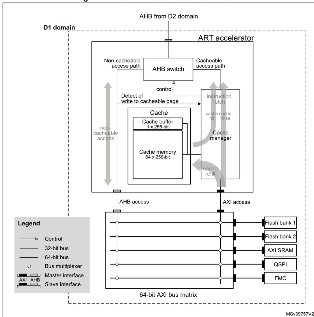
The block schematic illustrates the internal architecture of the ART accelerator and its connection to the system. The accelerator is contained within a dashed box labeled 'D1 domain'. At the top, an 'AHB from D2 domain' enters the domain. Inside, an 'AHB switch' directs traffic based on control signals from a 'Cache manager'. It has two primary paths: a 'Non-cacheable access path' leading to a 'non-cacheable access' port, and a 'Cacheable access path' leading to an 'instruction fetch' block. The 'instruction fetch' block interacts with the 'Cache manager' via 'cache cache hit miss' signals and receives 'cache refill' data. The 'Cache' block contains a 'Cache buffer 1 x 256-bit' and 'Cache memory 64 x 256-bit', and is also controlled by the 'Cache manager'. A 'Detect of write to cacheable page' signal is sent from the 'Cache' to the 'Cache manager'. Below the D1 domain, the 'non-cacheable access' path connects to an 'AHB access' port, and the 'instruction fetch' path connects to an 'AXI access' port. Both ports connect to a '64-bit AXI bus matrix'. This matrix is connected to several external components: 'Flash bank 1', 'Flash bank 2', 'AXI SRAM', 'QSPI', and 'FMC'. A 'Legend' in the bottom-left corner defines the symbols used: a thin line with an arrow for 'Control', a thin line for a '32-bit bus', a thick line for a '64-bit bus', a circle for a 'Bus multiplexer', and specific symbols for 'Master interface' (AXI and AHB) and 'Slave interface' (AXI and AHB). The identifier 'MSV39757V2' is located in the bottom-right corner of the diagram area.
6.3.2 ART accelerator blocks and operation
Instruction fetch accesses can be qualified as cacheable or non-cacheable. For cacheable accesses, the instruction fetch follows the cacheable access path. Non-cacheable accesses are directed to the master AHB port, following the non-cacheable access path. The appropriate access path is selected with the AHB switch controlled by the cache manager.
Cache
The cache contains a cache memory and a cache buffer.
The cache memory is organized in 64 lines of 256 bits each. Every line contains eight 32-bit segments. Each segment can contain one 32-bit or two 16-bit instruction codes.
The cache buffer is an extra line of 256 bits keeping a copy of one of cache lines (buffer source line). It allows fetching instruction code by the core while the corresponding buffer source line is in refill progress.
The ART accelerator keeps a 15-bit line index and a validity bit for each of 64 cache memory lines and for the cache buffer.
Cache manager
The cache manager:
- • checks whether the incoming memory instruction fetch access is cacheable
- • controls the AHB switch
- • for a cacheable access, checks for cache hit and allows instruction fetch from cache
- • manages the cache memory line refill (instruction code load) in case of cache miss
Check for cacheable access
Upon an access occurring on the slave AHB interface, the cache manager qualifies it as cacheable or non-cacheable. For an access to be qualified as cacheable, the following conditions must all be met:
- • the access is an instruction fetch (instruction code read)
- • the access is of 32-bit cacheable type (AHB properties)
- • the access address bits 31 through 20 (twelve MSB's) match the PCACHEADDR[11:0] field of the ART accelerator control register
Due to a pipelined architecture, the first cacheable access is handled as non-cacheable.
Check for cache hit
The cache manager checks for cache hit for every cacheable access.
For that effect, the cache manager simultaneously compares the address bits [19:5] of the pending instruction fetch access with the cache line and buffer indexes of the lines flagged as valid. Compare match indicates a cache hit. The absence of compare match indicates a cache miss.
This implementation allows the associativity of the cache memory lines with the 32-byte data blocks of the cacheable page without any interdependence, which maximizes the cache performance.
Upon a cache hit with a cache memory line:
- • The instruction code fetch from the cache line occurs.
- • The 256 bits of the line are instantly copied to the cache buffer.
Upon a cache hit with the cache buffer, the instruction code fetch from the cache buffer occurs.
In both cases, the bits [4:2] of the pending instruction fetch address are used as pointer to the cache line, to retrieve the instruction code from their corresponding 32-bit segment.
Figure 19. Instruction fetch from cache
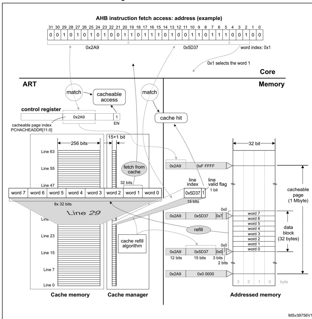
AHB instruction fetch access: address (example)
| 31 | 30 | 29 | 28 | 27 | 26 | 25 | 24 | 23 | 22 | 21 | 20 | 19 | 18 | 17 | 16 | 15 | 14 | 13 | 12 | 11 | 10 | 9 | 8 | 7 | 6 | 5 | 4 | 3 | 2 | 1 | 0 |
| 0 | 0 | 1 | 0 | 1 | 0 | 1 | 0 | 1 | 0 | 0 | 1 | 1 | 0 | 1 | 1 | 1 | 0 | 1 | 0 | 0 | 1 | 1 | 0 | 1 | 1 | 1 | 0 | 0 | 1 | 0 | 0 |
0x2A9 0x5D37 word index: 0x1
0x1 selects the word 1
Core
ART
Memory
Cache memory
Cache manager
Addressed memory
The diagram illustrates the instruction fetch process from the cache. At the top, a 32-bit AHB address is shown in binary, split into three parts: 0x2A9 (bits 31-20), 0x5D37 (bits 19-10), and word index 0x1 (bits 9-0). The word index 0x1 is used to select word 1 from a 32-bit data block. Below this, the Core is shown interacting with the ART (ART accelerator). The ART contains a control register with a cacheable page index (PCHACHEADDR[11:0]) set to 0x2A9 and an enable (EN) bit set to 1. The ART also includes a cache manager with a 'cacheable access' block and a 'cache hit' block. The cache manager uses the address to match against cache lines. The cache memory is organized into lines (e.g., Line 63, Line 55, Line 47, Line 29, Line 23, Line 15, Line 7, Line 0). Each line contains 256 bits of data and a 15+1 bit control field (15 bits for line index and 1 bit for line valid flag). Line 29 is shown in detail, containing 8x 32 bits of data (words 0-7). The cache manager also includes a 'fetch from cache' block and a 'cache refill algorithm'. The addressed memory is shown as a 32-bit wide memory with a 'cacheable page (1 Mbyte)' and 'data block (32 bytes)'. The diagram shows the flow of data from the address input, through the cache manager, into the cache memory, and finally to the addressed memory. The cache manager uses the address to match against cache lines and to select a cache line for refill. The cache refill algorithm is used to automatically select a cache memory line with data from the 32-byte data block of the target memory comprising the address of the AHB access.
MSV39756V1
Cache refill
Upon a cache miss:
- • A WRAP4 64-bit AXI access reaches the address of the AHB access in the target memory and fetches data directly to AHB via the cacheable access path.
- • Four successive WRAP4 64-bit AXI accesses refill the cache buffer and an automatically selected cache memory line with data from the 32-byte data block of the target memory comprising the address of the AHB access.
The cache buffer allows producing cache hits as soon as it is partially refilled (upon the first cycle of the WRAP4 access completed), which further increases the system efficiency.
When the cache memory is full upon a cache miss, a cache memory line must be evicted and replaced with new contents. The replacement policy is based on the LRU algorithm (least recently used).
Figure 19 illustrates an example of cache memory line refill, cache hit and instruction code fetch from the cache memory. For simplicity, the cache buffer is not represented.
Cache consistency
The following cases can cause the code in the cache to get inconsistent with the code on the corresponding address of the addressed memory:
- • A write access modifies a piece of data in the cacheable page of the addressed memory.
- • The software modifies the cacheable page index in the ART accelerator's control register.
- • A data transfer error occurs during the cache buffer and/or cache memory line refill.
The device incorporates a mechanism preventing software corruption due to the cache inconsistency. It detects the above cases and flags all the cache memory lines and the cache buffer as invalid. As a consequence, the following cacheable access results in cache miss and in subsequent cache buffer and cache line refill with new data.
6.4 ART accelerator registers
6.4.1 ART accelerator - control register (ART_CTR)
Address offset: 0x0000
Reset value: 0x0000 0004
| 31 | 30 | 29 | 28 | 27 | 26 | 25 | 24 | 23 | 22 | 21 | 20 | 19 | 18 | 17 | 16 |
|---|---|---|---|---|---|---|---|---|---|---|---|---|---|---|---|
| Res. | Res. | Res. | Res. | Res. | Res. | Res. | Res. | Res. | Res. | Res. | Res. | PCACHEADDR[11:8] | |||
| rw | rw | rw | rw | ||||||||||||
| 15 | 14 | 13 | 12 | 11 | 10 | 9 | 8 | 7 | 6 | 5 | 4 | 3 | 2 | 1 | 0 |
| PCACHEADDR[7:0] | Res. | Res. | Res. | Res. | Res. | Res. | Res. | EN | |||||||
| rw | rw | rw | rw | rw | rw | rw | rw | rw | |||||||
Bits 31:20 Reserved, must be kept at reset value.
Bits 19:8 PCACHEADDR[11:0] : cacheable page index
Base address of 1 Mbyte address page (cacheable page) from which the ART accelerator loads code to the cache. It can be modified with word (32-bit) access type. Other than 32-bit accesses have no effect.
Note: At runtime, it is recommended to disable the ART by clearing the EN bit before programming PCACHEADDR, then enable the ART again. There is no instruction loss when the ART is disabled.
Bits 7:1 Reserved, must be kept at reset value.
Bit 0 EN : cache enable
When enabled, the cache memory and refill mechanism operate. When disabled, all accesses default to non-cacheable.
0x1: enable
0x0: disable
Refer to Section 2.3 on page 134 for the register boundary addresses.