36. Tamper and backup registers (TAMP) applied to STM32L41xxx and STM32L42xxx devices only
36.1 Introduction
32 32-bit backup registers are retained in all low-power modes and also in \( V_{BAT} \) mode. They can be used to store sensitive data as their content is protected by an tamper detection circuit. 2 tamper pins are available for anti-tamper detection. The external tamper pins can be configured for edge detection, or level detection with or without filtering.
36.2 TAMP main features
- • 32 backup registers:
- – the backup registers (TAMP_BKPxR) are implemented in the RTC domain that remains powered-on by \( V_{BAT} \) when the \( V_{DD} \) power is switched off.
- • 2 external tamper detection events.
- – External passive tampers with configurable filter and internal pull-up.
- • Any tamper detection can generate a RTC timestamp event.
- • Any tamper detection can erase the backup registers.
36.3 TAMP functional description
36.3.1 TAMP block diagram
Figure 357. TAMP block diagram
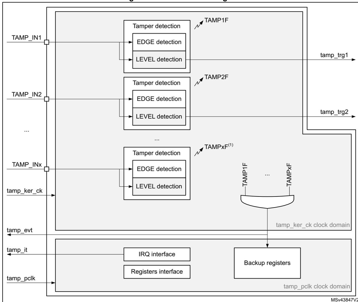
The diagram illustrates the internal architecture of the TAMP block. On the left, external pins are shown: TAMP_IN1, TAMP_IN2, an ellipsis, TAMP_INx, tamp_ker_ck, tamp_evt, tamp_it, and tamp_pclk. The TAMP_IN pins connect to individual 'Tamper detection' blocks. Each block contains 'EDGE detection' and 'LEVEL detection' sub-blocks. These sub-blocks output flags: TAMP1F, TAMP2F, and TAMPxF (1) . These flags are inputs to a large OR gate. The output of the OR gate is connected to the 'Backup registers' block and also to the tamp_trg1 and tamp_trg2 pins. The tamp_ker_ck pin provides a clock signal to the 'Backup registers' block, which is labeled as the 'tamp_ker_ck clock domain'. The tamp_pclk pin provides a clock signal to the 'IRQ interface' and 'Registers interface' blocks, which are labeled as the 'tamp_pclk clock domain'. The 'Backup registers' block is also connected to the 'IRQ interface' and 'Registers interface' blocks. The 'IRQ interface' and 'Registers interface' blocks are connected to the tamp_it and tamp_pclk pins. The tamp_evt pin is an output from the 'Backup registers' block. The diagram is labeled with MSv43847V2 at the bottom right.
1. The number of external tampers depends on products.
36.3.2 TAMP pins and internal signals
Table 183. TAMP input/output pins
| Pin name | Signal type | Description |
|---|---|---|
| TAMP_INx (x = pin index) | Input | Tamper input pin |
Table 184. TAMP internal input/output signals
| Internal signal name | Signal type | Description |
|---|---|---|
| tamp_ker_ck | Input | TAMP kernel clock, connected to rtc_ker_ck and also named RTCCLK in this document |
| tamp_pclk | Input | TAMP APB clock, connected to rtc_pclk |
| tamp_evt | Output | Tamper event detection (internal or external) The tamp_evt is used to generate a RTC timestamp event |
| tamp_erase | Output | Device secrets erase request following either tamper event detection (internal or external) or the software erase request done by writing BKERASE to 1 |
| tamp_it | Output | TAMP interrupt (refer to Section 36.5: TAMP interrupts for details) |
| tamp_trg[x] (x = signal index) | Output | Tamper detection trigger |
The TAMP kernel clock is usually the LSE at 32.768 kHz although it is possible to select other clock sources in the RCC (refer to RCC for more details). Some detections modes are not available in some low-power modes or \( V_{BAT} \) when the selected clock is not LSE (refer to Section 36.4: TAMP low-power modes for more details).
Table 185. TAMP interconnection
| Signal name | Source/Destination |
|---|---|
| tamp_evt | rtc_tamp_evt used to generate a timestamp event |
| tamp_erase | The tamp_erase signal is used to erase the device secrets listed hereafter: backup registers |
36.3.3 TAMP register write protection
After system reset, the TAMP registers (including backup registers) are protected against parasitic write access by the DBP bit in the power control peripheral (refer to the PWR power control section). DBP bit must be set in order to enable TAMP registers write access.
36.3.4 Tamper detection
The tamper detection can be configured for the following purposes:
- • erase the backup registers (default configuration)
- • generate an interrupt, capable to wake up from Stop and Standby mode
- • generate a hardware trigger for the low-power timers
TAMP backup registers
The backup registers (TAMP_BKPxR) are not reset by system reset or when the device wakes up from Standby mode.
The backup registers are reset when a tamper detection event occurs except if the TAMPxNOER bit is set, or if the TAMPxMSK is set in the TAMP_CR2 register.
The backup registers can be reset by software by setting the BKERASE bit in the TAMP_CR2 register.
Note: The backup registers are also erased when the readout protection of the flash is changed from level 1 to level 0.
Tamper detection initialization
Each input can be enabled by setting the corresponding TAMPxE bits to 1 in the TAMP_CR register.
Each TAMP_INx tamper detection input is associated with a flag TAMPxF in the TAMP_SR register.
When TAMPxMSK is cleared:
The TAMPxF flag is asserted after the tamper event on the pin, with the latency provided below:
- • 3 ck_apre cycles when TAMPFLT differs from 0x0 (level detection with filtering)
- • 3 ck_apre cycles when TAMPTS = 1 (timestamp on tamper event)
- • No latency when TAMPFLT = 0x0 (edge detection) and TAMPTS = 0
A new tamper occurring on the same pin during this period and as long as TAMPxF is set cannot be detected.
When TAMPxMSK is set:
A new tamper occurring on the same pin cannot be detected during the latency described above and 2.5 ck_rtc additional cycles.
By setting the TAMPxIE bit in the TAMP_IER register, an interrupt is generated when a tamper detection event occurs (when TAMPxF is set). Setting TAMPxIE is not allowed when the corresponding TAMPxMSK is set.
Trigger output generation on tamper event
The tamper event detection can be used as trigger input by the low-power timers.
When TAMPxMSK bit is cleared in TAMP_CR register, the TAMPxF flag must be cleared by software in order to allow a new tamper detection on the same pin.
When TAMPxMSK bit is set, the TAMPxF flag is masked, and kept cleared in TAMP_SR register. This configuration allows the low-power timers in Stop mode to be triggered automatically, without requiring the system wake-up to perform the TAMPxF clearing. In this case, the backup registers are not cleared.
This feature is available only when the tamper is configured in the Level detection with filtering on tamper inputs (passive mode) mode.
Timestamp on tamper event
With TAMPTS set to 1 in the RTC_CR, any tamper event causes a timestamp to occur. In this case, either the TSF bit or the TSOVF bit is set in RTC_SR, in the same manner as if a normal timestamp event occurs. The affected tamper flag register TAMPxF is set in the TAMP_SR at the same time that TSF or TSOVF is set in the RTC_SR.
Edge detection on tamper inputs (passive mode)
If the TAMPFLT bits are 00, the TAMP_INx pins generate tamper detection events when either a rising edge/high level or a falling edge/low level is observed depending on the corresponding TAMPxTRG bit. The internal pull-up resistors on the TAMP_INx inputs are deactivated when edge detection is selected.
Caution:
When using the edge detection, it is recommended to check by software the tamper pin level just after enabling the tamper detection (by reading the GPIO registers), and before writing sensitive values in the backup registers, to ensure that an active edge did not occur before enabling the tamper event detection.
When TAMPFLT = 00 and TAMPxTRG = 0 (rising edge detection), a tamper event may be detected by hardware if the tamper input is already at high level before enabling the tamper detection.
After a tamper event has been detected and cleared, the TAMP_INx should be disabled and then re-enabled (TAMPxE set to 1) before re-programming the backup registers (TAMP_BKPxR). This prevents the application from writing to the backup registers while the TAMP_INx input value still indicates a tamper detection. This is equivalent to a level detection on the TAMP_INx input.
Note: Tamper detection is still active when \( V_{DD} \) power is switched off. To avoid unwanted resetting of the backup registers, the pin to which the TAMPx is mapped should be externally tied to the correct level.
Level detection with filtering on tamper inputs (passive mode)
Level detection with filtering is performed by setting TAMPFLT to a non-zero value. A tamper detection event is generated when either 2, 4, or 8 (depending on TAMPFLT) consecutive samples are observed at the level designated by the TAMPxTRG bits.
The TAMP_INx inputs are precharged through the I/O internal pull-up resistance before its state is sampled, unless disabled by setting TAMPPUDIS to 1. The duration of the precharge is determined by the TAMPPRCH bits, allowing for larger capacitances on the TAMP_INx inputs.
The trade-off between tamper detection latency and power consumption through the pull-up can be optimized by using TAMPFREQ to determine the frequency of the sampling for level detection.
Note: Refer to the microcontroller datasheet for the electrical characteristics of the pull-up resistors.
36.4 TAMP low-power modes
Table 186. Effect of low-power modes on TAMP
| Mode | Description |
|---|---|
| Sleep | No effect. TAMP interrupts cause the device to exit the Sleep mode. |
| Stop | No effect on all features, except for level detection with filtering mode which remain active only when the clock source is LSE or LSI. Tamper events cause the device to exit the Stop mode. |
| Standby | No effect on all features, except for level detection with filtering mode which remain active only when the clock source is LSE or LSI. Tamper events cause the device to exit the Standby mode. |
| Shutdown | No effect on all features, except for level detection with filtering mode which remain active only when the clock source is LSE. Tamper events cause the device to exit the Shutdown mode. |
36.5 TAMP interrupts
The interrupt channel is set in the interrupt status register. The interrupt output is also activated.
Table 187. Interrupt requests
| Interrupt acronym | Interrupt event | Event flag (1) | Enable control bit (2) | Interrupt clear method | Exit from Sleep mode | Exit from Stop and Standby modes | Exit from Shutdown mode |
|---|---|---|---|---|---|---|---|
| TAMP | Tamper x (3) | TAMPxF | TAMPxE | Write 1 in CTAMPxF | Yes | Yes (4) | Yes (5) |
- 1. The event flags are in the TAMP_SR register.
- 2. The interrupt masked flags (resulting from event flags AND enable control bits) are in the TAMP_MISR register.
- 3. The number of tampers events depend on products.
- 4. In case of level detection with filtering passive tamper mode, wake-up from Stop and Standby modes is possible only when the TAMP clock source is LSE or LSI.
- 5. In case of level detection with filtering passive tamper mode, wake-up from Shutdown modes is possible only when the TAMP clock source is LSE.
36.6 TAMP registers
Refer to Section 1.2 on page 64 of the reference manual for a list of abbreviations used in register descriptions. The peripheral registers can be accessed by words (32-bit).
36.6.1 TAMP control register 1 (TAMP_CR1)
Address offset: 0x00
Backup domain reset value: 0xFFFF 0000
System reset: not affected
| 31 | 30 | 29 | 28 | 27 | 26 | 25 | 24 | 23 | 22 | 21 | 20 | 19 | 18 | 17 | 16 |
|---|---|---|---|---|---|---|---|---|---|---|---|---|---|---|---|
| Res. | Res. | Res. | Res. | Res. | Res. | Res. | Res. | Res. | Res. | Res. | Res. | Res. | Res. | Res. | Res. |
| 15 | 14 | 13 | 12 | 11 | 10 | 9 | 8 | 7 | 6 | 5 | 4 | 3 | 2 | 1 | 0 |
| Res. | Res. | Res. | Res. | Res. | Res. | Res. | Res. | Res. | Res. | Res. | Res. | Res. | Res. | TAMP2 E | TAMP1 E |
| rw | rw |
Bits 31:24 Reserved, must be kept at reset value.
Bit 23 Reserved, must be kept at reset value.
Bit 22 Reserved, must be kept at reset value.
Bit 21 Reserved, must be kept at reset value.
Bit 20 Reserved, must be kept at reset value.
Bit 19 Reserved, must be kept at reset value.
Bit 18 Reserved, must be kept at reset value.
Bit 17 Reserved, must be kept at reset value.
Bit 16 Reserved, must be kept at reset value.
Bits 15:2 Reserved, must be kept at reset value.
Bit 1 TAMP2E : Tamper detection on TAMP_IN2 enable (1)
0: Tamper detection on TAMP_IN2 is disabled.
1: Tamper detection on TAMP_IN2 is enabled.
Bit 0 TAMP1E : Tamper detection on TAMP_IN1 enable (1)
0: Tamper detection on TAMP_IN1 is disabled.
1: Tamper detection on TAMP_IN1 is enabled.
- 1. Tamper detection mode (selected with TAMP_FLTCR register and TAMPxTRG bits in TAMP_CR2), must be configured before enabling the tamper detection.
36.6.2 TAMP control register 2 (TAMP_CR2)
Address offset: 0x04
Backup domain reset value: 0x0000 0000
System reset: not affected
| 31 | 30 | 29 | 28 | 27 | 26 | 25 | 24 | 23 | 22 | 21 | 20 | 19 | 18 | 17 | 16 |
|---|---|---|---|---|---|---|---|---|---|---|---|---|---|---|---|
| Res. | Res. | Res. | Res. | Res. | Res. | TAMP2 TRG | TAMP1 TRG | BK ERASE | Res. | Res. | Res. | Res. | Res. | TAMP2 MSK | TAMP1 MSK |
| rw | rw | w | rw | rw | |||||||||||
| 15 | 14 | 13 | 12 | 11 | 10 | 9 | 8 | 7 | 6 | 5 | 4 | 3 | 2 | 1 | 0 |
| Res. | Res. | Res. | Res. | Res. | Res. | Res. | Res. | Res. | Res. | Res. | Res. | Res. | Res. | TAMP2 NOER | TAMP1 NOER |
| rw | rw |
Bits 31:26 Reserved, must be kept at reset value.
Bit 25 TAMP2TRG : Active level for tamper 2 input
- 0: If TAMPFLT ≠ 00 Tamper 2 input staying low triggers a tamper detection event.
If TAMPFLT = 00 Tamper 2 input rising edge and high level triggers a tamper detection event. - 1: If TAMPFLT ≠ 00 Tamper 2 input staying high triggers a tamper detection event.
If TAMPFLT = 00 Tamper 2 input falling edge and low level triggers a tamper detection event.
Bit 24 TAMP1TRG : Active level for tamper 1 input
- 0: If TAMPFLT ≠ 00 Tamper 1 input staying low triggers a tamper detection event.
If TAMPFLT = 00 Tamper 1 input rising edge and high level triggers a tamper detection event. - 1: If TAMPFLT ≠ 00 Tamper 1 input staying high triggers a tamper detection event.
If TAMPFLT = 00 Tamper 1 input falling edge and low level triggers a tamper detection event.
Bit 23 BKERASE : Backup registers erase
Writing '1' to this bit reset the backup registers. Writing 0 has no effect. This bit is always read as 0.
Bits 22:18 Reserved, must be kept at reset value.
Bit 17 TAMP2MSK : Tamper 2 mask
- 0: Tamper 2 event generates a trigger event and TAMP2F must be cleared by software to allow next tamper event detection.
- 1: Tamper 2 event generates a trigger event. TAMP2F is masked and internally cleared by hardware. The backup registers are not erased.
The tamper 2 interrupt must not be enabled when TAMP2MSK is set.
Bit 16 TAMP1MSK : Tamper 1 mask
- 0: Tamper 1 event generates a trigger event and TAMP1F must be cleared by software to allow next tamper event detection.
- 1: Tamper 1 event generates a trigger event. TAMP1F is masked and internally cleared by hardware. The backup registers are not erased.
The tamper 1 interrupt must not be enabled when TAMP1MSK is set.
Bits 15:2 Reserved, must be kept at reset value.
Bit 1 TAMP2NOER : Tamper 2 no erase
0: Tamper 2 event erases the backup registers.
1: Tamper 2 event does not erase the backup registers.
Bit 0 TAMP1NOER : Tamper 1 no erase
0: Tamper 1 event erases the backup registers.
1: Tamper 1 event does not erase the backup registers.
36.6.3 TAMP filter control register (TAMP_FLTCR)
Address offset: 0x0C
Backup domain reset value: 0x0000 0000
System reset: not affected
| 31 | 30 | 29 | 28 | 27 | 26 | 25 | 24 | 23 | 22 | 21 | 20 | 19 | 18 | 17 | 16 |
|---|---|---|---|---|---|---|---|---|---|---|---|---|---|---|---|
| Res. | Res. | Res. | Res. | Res. | Res. | Res. | Res. | Res. | Res. | Res. | Res. | Res. | Res. | Res. | Res. |
| 15 | 14 | 13 | 12 | 11 | 10 | 9 | 8 | 7 | 6 | 5 | 4 | 3 | 2 | 1 | 0 |
| Res. | Res. | Res. | Res. | Res. | Res. | Res. | Res. | TAMP PUDIS | TAMPPRCH [1:0] | TAMPFLT [1:0] | TAMPFREQ [2:0] | ||||
| rw | rw | rw | rw | rw | rw | rw | rw | ||||||||
Bits 31:8 Reserved, must be kept at reset value.
Bit 7 TAMPPUDIS : TAMP_INx pull-up disable
This bit determines if each of the TAMPx pins are precharged before each sample.
0: Precharge TAMP_INx pins before sampling (enable internal pull-up)
1: Disable precharge of TAMP_INx pins.
Bits 6:5 TAMPPRCH[1:0] : TAMP_INx precharge duration
These bits determine the duration of time during which the pull-up is activated before each sample. TAMPPRCH is valid for each of the TAMP_INx inputs.
- 0x0: 1 RTCCLK cycle
- 0x1: 2 RTCCLK cycles
- 0x2: 4 RTCCLK cycles
- 0x3: 8 RTCCLK cycles
Bits 4:3 TAMPFLT[1:0] : TAMP_INx filter count
These bits determine the number of consecutive samples at the specified level (TAMP*TRG) needed to activate a tamper event. TAMPFLT is valid for each of the TAMP_INx inputs.
- 0x0: Tamper event is activated on edge of TAMP_INx input transitions to the active level (no internal pull-up on TAMP_INx input).
- 0x1: Tamper event is activated after 2 consecutive samples at the active level.
- 0x2: Tamper event is activated after 4 consecutive samples at the active level.
- 0x3: Tamper event is activated after 8 consecutive samples at the active level.
Bits 2:0 TAMPFREQ[2:0] : Tamper sampling frequency
Determines the frequency at which each of the TAMP_INx inputs are sampled.
- 0x0: RTCCLK / 32768 (1 Hz when RTCCLK = 32768 Hz)
- 0x1: RTCCLK / 16384 (2 Hz when RTCCLK = 32768 Hz)
- 0x2: RTCCLK / 8192 (4 Hz when RTCCLK = 32768 Hz)
- 0x3: RTCCLK / 4096 (8 Hz when RTCCLK = 32768 Hz)
- 0x4: RTCCLK / 2048 (16 Hz when RTCCLK = 32768 Hz)
- 0x5: RTCCLK / 1024 (32 Hz when RTCCLK = 32768 Hz)
- 0x6: RTCCLK / 512 (64 Hz when RTCCLK = 32768 Hz)
- 0x7: RTCCLK / 256 (128 Hz when RTCCLK = 32768 Hz)
Note: This register concerns only the tamper inputs in passive mode.
36.6.4 TAMP interrupt enable register (TAMP_IER)
Address offset: 0x2C
Backup domain reset value: 0x0000 0000
System reset: not affected
| 31 | 30 | 29 | 28 | 27 | 26 | 25 | 24 | 23 | 22 | 21 | 20 | 19 | 18 | 17 | 16 |
|---|---|---|---|---|---|---|---|---|---|---|---|---|---|---|---|
| Res. | Res. | Res. | Res. | Res. | Res. | Res. | Res. | Res. | Res. | Res. | Res. | Res. | Res. | Res. | Res. |
| 15 | 14 | 13 | 12 | 11 | 10 | 9 | 8 | 7 | 6 | 5 | 4 | 3 | 2 | 1 | 0 |
| Res. | Res. | Res. | Res. | Res. | Res. | Res. | Res. | Res. | Res. | Res. | Res. | Res. | Res. | TAMP 2IE | TAMP 1IE |
| rw | rw |
Bits 31:24 Reserved, must be kept at reset value.
Bit 23 Reserved, must be kept at reset value.
Bit 22 Reserved, must be kept at reset value.
Bit 21 Reserved, must be kept at reset value.
Bit 20 Reserved, must be kept at reset value.
- Bit 19 Reserved, must be kept at reset value.
- Bit 18 Reserved, must be kept at reset value.
- Bit 17 Reserved, must be kept at reset value.
- Bit 16 Reserved, must be kept at reset value.
- Bits 15:2 Reserved, must be kept at reset value.
- Bit 1
TAMP2IE
: Tamper 2 interrupt enable
- 0: Tamper 2 interrupt disabled.
- 1: Tamper 2 interrupt enabled.
- Bit 0
TAMP1IE
: Tamper 1 interrupt enable
- 0: Tamper 1 interrupt disabled.
- 1: Tamper 1 interrupt enabled.
36.6.5 TAMP status register (TAMP_SR)
Address offset: 0x30
Backup domain reset value: 0x0000 0000
System reset: not affected
| 31 | 30 | 29 | 28 | 27 | 26 | 25 | 24 | 23 | 22 | 21 | 20 | 19 | 18 | 17 | 16 |
|---|---|---|---|---|---|---|---|---|---|---|---|---|---|---|---|
| Res. | Res. | Res. | Res. | Res. | Res. | Res. | Res. | Res. | Res. | Res. | Res. | Res. | Res. | Res. | Res. |
| 15 | 14 | 13 | 12 | 11 | 10 | 9 | 8 | 7 | 6 | 5 | 4 | 3 | 2 | 1 | 0 |
| Res. | Res. | Res. | Res. | Res. | Res. | Res. | Res. | Res. | Res. | Res. | Res. | Res. | Res. | TAMP 2F | TAMP 1F |
| r | r |
- Bits 31:24 Reserved, must be kept at reset value.
- Bit 23 Reserved, must be kept at reset value.
- Bit 22 Reserved, must be kept at reset value.
- Bit 21 Reserved, must be kept at reset value.
- Bit 20 Reserved, must be kept at reset value.
- Bit 19 Reserved, must be kept at reset value.
- Bit 18 Reserved, must be kept at reset value.
- Bit 17 Reserved, must be kept at reset value.
- Bit 16 Reserved, must be kept at reset value.
- Bits 15:2 Reserved, must be kept at reset value.
- Bit 1
TAMP2F
: TAMP2 detection flag
- This flag is set by hardware when a tamper detection event is detected on the TAMP2 input.
- Bit 0
TAMP1F
: TAMP1 detection flag
- This flag is set by hardware when a tamper detection event is detected on the TAMP1 input.
36.6.6 TAMP masked interrupt status register (TAMP_MISR)
Address offset: 0x34
Backup domain reset value: 0x0000 0000
System reset: not affected
| 31 | 30 | 29 | 28 | 27 | 26 | 25 | 24 | 23 | 22 | 21 | 20 | 19 | 18 | 17 | 16 |
|---|---|---|---|---|---|---|---|---|---|---|---|---|---|---|---|
| Res. | Res. | Res. | Res. | Res. | Res. | Res. | Res. | Res. | Res. | Res. | Res. | Res. | Res. | Res. | Res. |
| 15 | 14 | 13 | 12 | 11 | 10 | 9 | 8 | 7 | 6 | 5 | 4 | 3 | 2 | 1 | 0 |
| Res. | Res. | Res. | Res. | Res. | Res. | Res. | Res. | Res. | Res. | Res. | Res. | Res. | Res. | TAMP 2MF | TAMP 1MF |
| r | r |
Bits 31:24 Reserved, must be kept at reset value.
Bit 23 Reserved, must be kept at reset value.
Bit 22 Reserved, must be kept at reset value.
Bit 21 Reserved, must be kept at reset value.
Bit 20 Reserved, must be kept at reset value.
Bit 19 Reserved, must be kept at reset value.
Bit 18 Reserved, must be kept at reset value.
Bit 17 Reserved, must be kept at reset value.
Bit 16 Reserved, must be kept at reset value.
Bits 15:2 Reserved, must be kept at reset value.
Bit 1 TAMP2MF : TAMP2 interrupt masked flag
This flag is set by hardware when the tamper 2 interrupt is raised.
Bit 0 TAMP1MF : TAMP1 interrupt masked flag
This flag is set by hardware when the tamper 1 interrupt is raised.
36.6.7 TAMP status clear register (TAMP_SCR)
Address offset: 0x3C
System reset value: 0x0000 0000
| 31 | 30 | 29 | 28 | 27 | 26 | 25 | 24 | 23 | 22 | 21 | 20 | 19 | 18 | 17 | 16 |
|---|---|---|---|---|---|---|---|---|---|---|---|---|---|---|---|
| Res. | Res. | Res. | Res. | Res. | Res. | Res. | Res. | Res. | Res. | Res. | Res. | Res. | Res. | Res. | Res. |
| 15 | 14 | 13 | 12 | 11 | 10 | 9 | 8 | 7 | 6 | 5 | 4 | 3 | 2 | 1 | 0 |
| Res. | Res. | Res. | Res. | Res. | Res. | Res. | Res. | Res. | Res. | Res. | Res. | Res. | Res. | CTAMP 2F | CTAMP 1F |
| w | w |
- Bits 31:24 Reserved, must be kept at reset value.
- Bit 23 Reserved, must be kept at reset value.
- Bit 22 Reserved, must be kept at reset value.
- Bit 21 Reserved, must be kept at reset value.
- Bit 20 Reserved, must be kept at reset value.
- Bit 19 Reserved, must be kept at reset value.
- Bit 18 Reserved, must be kept at reset value.
- Bit 17 Reserved, must be kept at reset value.
- Bit 16 Reserved, must be kept at reset value.
- Bits 15:2 Reserved, must be kept at reset value.
- Bit 1
CTAMP2F
: Clear TAMP2 detection flag
- Writing 1 in this bit clears the TAMP2F bit in the TAMP_SR register.
- Bit 0
CTAMP1F
: Clear TAMP1 detection flag
- Writing 1 in this bit clears the TAMP1F bit in the TAMP_SR register.
36.6.8 TAMP backup x register (TAMP_BKPxR)
Address offset: 0x100 + 0x04 * x, (x = 0 to 31)
Backup domain reset value: 0x0000 0000
System reset: not affected
| 31 | 30 | 29 | 28 | 27 | 26 | 25 | 24 | 23 | 22 | 21 | 20 | 19 | 18 | 17 | 16 |
|---|---|---|---|---|---|---|---|---|---|---|---|---|---|---|---|
| BKP[31:16] | |||||||||||||||
| rw | rw | rw | rw | rw | rw | rw | rw | rw | rw | rw | rw | rw | rw | rw | rw |
| 15 | 14 | 13 | 12 | 11 | 10 | 9 | 8 | 7 | 6 | 5 | 4 | 3 | 2 | 1 | 0 |
| BKP[15:0] | |||||||||||||||
| rw | rw | rw | rw | rw | rw | rw | rw | rw | rw | rw | rw | rw | w | rw | rw |
Bits 31:0 BKP[31:0]:
The application can write or read data to and from these registers.
They are powered-on by V BAT when V DD is switched off, so that they are not reset by System reset, and their contents remain valid when the device operates in low-power mode.
In the default configuration this register is reset on a tamper detection event. It is forced to reset value as long as there is at least one external tamper flag being set. This register is also reset when the readout protection (RDP) is disabled.
36.6.9 TAMP register map
Table 188. TAMP register map and reset values
| Offset | Register | 31 | 30 | 29 | 28 | 27 | 26 | 25 | 24 | 23 | 22 | 21 | 20 | 19 | 18 | 17 | 16 | 15 | 14 | 13 | 12 | 11 | 10 | 9 | 8 | 7 | 6 | 5 | 4 | 3 | 2 | 1 | 0 | |
|---|---|---|---|---|---|---|---|---|---|---|---|---|---|---|---|---|---|---|---|---|---|---|---|---|---|---|---|---|---|---|---|---|---|---|
| 0x00 | TAMP_CR1 | Res. | Res. | Res. | Res. | Res. | Res. | Res. | Res. | Res. | Res. | Res. | Res. | Res. | Res. | Res. | Res. | Res. | Res. | Res. | Res. | Res. | Res. | Res. | Res. | Res. | Res. | Res. | Res. | Res. | Res. | Res. | TAMP2E | TAMP1E |
| Reset value | 0 | 0 | ||||||||||||||||||||||||||||||||
| 0x04 | TAMP_CR2 | Res. | Res. | Res. | Res. | Res. | Res. | TAMP2TRG | TAMP1TRG | BKERASE | Res. | Res. | Res. | Res. | Res. | TAMP2MSK | TAMP1MSK | Res. | Res. | Res. | Res. | Res. | Res. | Res. | Res. | Res. | Res. | Res. | Res. | Res. | Res. | Res. | TAMP2NOER | TAMP1NOER |
| Reset value | 0 | 0 | 0 | 0 | 0 | 0 | 0 | |||||||||||||||||||||||||||
| 0x0C | TAMP_FLTCR | Res. | Res. | Res. | Res. | Res. | Res. | Res. | Res. | Res. | Res. | Res. | Res. | Res. | Res. | Res. | Res. | Res. | Res. | Res. | Res. | Res. | Res. | Res. | Res. | TAMPPLUDIS | TAMP2PRCH[1:0] | TAMPFLT[1:0] | TAMPFREQ[2:0] | |||||
| Reset value | 0 | 0 | 0 | 0 | 0 | 0 | 0 | 0 | ||||||||||||||||||||||||||
| 0x2C | TAMP_IER | Res. | Res. | Res. | Res. | Res. | Res. | Res. | Res. | Res. | Res. | Res. | Res. | Res. | Res. | Res. | Res. | Res. | Res. | Res. | Res. | Res. | Res. | Res. | Res. | Res. | Res. | Res. | Res. | Res. | Res. | Res. | TAMP2IE | TAMP1IE |
| Reset value | 0 | 0 | ||||||||||||||||||||||||||||||||
| 0x30 | TAMP_SR | Res. | Res. | Res. | Res. | Res. | Res. | Res. | Res. | Res. | Res. | Res. | Res. | Res. | Res. | Res. | Res. | Res. | Res. | Res. | Res. | Res. | Res. | Res. | Res. | Res. | Res. | Res. | Res. | Res. | Res. | Res. | TAMP2F | TAMP1F |
| Reset value | 0 | 0 | ||||||||||||||||||||||||||||||||
| 0x34 | TAMP_MISR | Res. | Res. | Res. | Res. | Res. | Res. | Res. | Res. | Res. | Res. | Res. | Res. | Res. | Res. | Res. | Res. | Res. | Res. | Res. | Res. | Res. | Res. | Res. | Res. | Res. | Res. | Res. | Res. | Res. | Res. | Res. | TAMP2MF | TAMP1MF |
| Reset value | 0 | 0 | ||||||||||||||||||||||||||||||||
| 0x3C | TAMP_SCR | Res. | Res. | Res. | Res. | Res. | Res. | Res. | Res. | Res. | Res. | Res. | Res. | Res. | Res. | Res. | Res. | Res. | Res. | Res. | Res. | Res. | Res. | Res. | Res. | Res. | Res. | Res. | Res. | Res. | Res. | Res. | CTAMP2F | CTAMP1F |
| Reset value | 0 | 0 | ||||||||||||||||||||||||||||||||
| 0x100 + 0x04*x, (x= 0 to 31) | TAMP_BKPxR | BKP[31:0] | ||||||||||||||||||||||||||||||||
| Reset value | 0 | 0 | 0 | 0 | 0 | 0 | 0 | 0 | 0 | 0 | 0 | 0 | 0 | 0 | 0 | 0 | 0 | 0 | 0 | 0 | 0 | 0 | 0 | 0 | 0 | 0 | 0 | 0 | 0 | 0 | 0 | 0 | ||
Refer to Section 2.2 for the register boundary addresses.