22. Liquid crystal display controller (LCD)
This section applies to STM32L4x3xx devices only.
22.1 LCD introduction
The LCD controller is a digital controller/driver for monochrome passive liquid crystal display (LCD) with up to eight common terminals, and up to 44 segment terminals to drive 176 (44x4) or 320 (40x8) LCD picture elements (pixels). The exact number of terminals depends on the device pinout as described in the datasheet.
The LCD is made up of several segments (pixels or complete symbols) that can be turned visible or invisible. Each segment consists of a layer of liquid crystal molecules aligned between two electrodes. When a voltage greater than a threshold voltage is applied across the liquid crystal, the segment becomes visible. The segment voltage must be alternated to avoid an electrophoresis effect in the liquid crystal (which degrades the display). The waveform across a segment must then be generated, so to avoid having a direct current (DC).
Glossary
Bias: number of voltage levels used when driving an LCD
It is defined as \( 1 / (\text{number of voltage levels used to drive an LCD display} - 1) \) .
Boost circuit: contrast controller circuit
Common: electrical connection terminal connected to several segments (44 segments)
Duty ratio: number defined as \( 1 / (\text{number of common terminals on a given LCD display}) \)
Frame: one period of the waveform written to a segment
Frame rate: number of frames per second (number of times the LCD segments are energized per second)
LCD (liquid crystal display): passive display panel with terminals leading directly to a segment
Segment: smallest viewing element (a single bar or dot that is used to help create a character on an LCD display)
22.2 LCD main features
- • Highly flexible frame rate control
- • Static, 1/2, 1/3, 1/4, and 1/8 duty supported
- • Static, 1/2, 1/3, and 1/4 bias supported
- • Double-buffered memory allowing data in LCD_RAM registers to be updated at any time by the application firmware without affecting the integrity of the data displayed
- – LCD data RAM of up to 16 x 32-bit registers, which contain pixel information (active/inactive)
- • Software selectable LCD output voltage (contrast) from \( V_{LCDmin} \) to \( V_{LCDmax} \)
- • No need for external analog components:
- – Step-up converter, embedded to generate an internal \( V_{LCD} \) voltage higher than \( V_{DD} \)
- – Software selection between external and internal \( V_{LCD} \) voltage source. In case of an external source, the internal boost circuit is disabled to reduce power consumption.
- – Resistive network, embedded to generate intermediate \( V_{LCD} \) voltages
- – Structure of the resistive network configurable by software to adapt the power consumption to match the capacitive charge required by the LCD panel
- – Integrated voltage output buffers for higher LCD driving capability.
- • Contrast that can be adjusted using two different methods:
- – When using the internal step-up converter, the software can adjust \( V_{LCD} \) between \( V_{LCDmin} \) and \( V_{LCDmax} \) .
- – Programmable dead time (up to eight phase periods) between frames
- • Full support of low-power modes: The LCD controller can be displayed in Sleep, Low-power run, Low-power sleep, and Stop modes, or can be fully disabled to reduce power consumption.
- • Built-in phase inversion for reduced power consumption and EMI (electromagnetic interference)
- • Start-of-frame interrupt to synchronize the software when updating the LCD data RAM
- • Blink capability:
- – Up to 1, 2, 3, 4, 8, or all pixels which can be programmed to blink at a configurable frequency
- – Software adjustable blink frequency to achieve around 0.5 Hz, 1 Hz, 2 Hz, or 4 Hz
- • Used LCD segment and common pins must be configured as GPIO alternate functions, and unused segment and common pins can be used for GPIO or for another peripheral alternate function.
Note: When the LCD relies on the internal stepup converter, the VLCD pin must be connected to \( V_{SS} \) with a capacitor. Its typical value is 1 \( \mu F \) (see \( C_{EXT} \) value in the datasheet for details).
22.3 LCD functional description
22.3.1 General description
The LCD controller has five main blocks (see Figure 134 ):
Figure 134. LCD controller block diagram
![Figure 134. LCD controller block diagram. The diagram shows the internal architecture of the LCD controller. On the left, an 'Address bus' and 'Data bus' are shown. The 'Data bus' connects to 'LCD regs', 'LCD RAM (32x16 bits)', and another 'LCD regs' block. The 'LCD RAM' output goes to an '8-to-1 mux', which then connects to a 'SEG driver'. The 'SEG driver' output (labeled 'SEG[43:0]' and '44') connects to an 'Analog switch array'. The 'Analog switch array' has multiple output lines: COM0 through COM3, SEG0 through SEG39, SEG40/COM4, SEG41/COM5, SEG42/COM6, and SEG43/COM7. Above the 'SEG driver', a 'COM driver' block receives 'ck_div' and 'READY' signals and outputs 'COM[3:0]' and 'COM[7:4]'. A 'Frequency generator' block contains a '16-bit prescaler' (input LCDCLK, output LCDCLK/32768), a 'CLOCK MUX' (inputs PS[3:0] and LCDCLK/32768, output ck_ps), and a 'Divide by 16 to 31' block (input DIV[3:0] and ck_ps, output ck_div). Below the 'SEG driver', a 'Pulse generator' (input STATIC) and 'LCD regs' (input VSEL) connect to an 'Analog stepup converter' block. This block contains a 'Voltage generator' (inputs EN, HD, BIAS[1:0], CC[2:0]) and a 'Contrast controller' (input VCC). The 'Voltage generator' outputs Vss, 1/3-1/4 Vcc, 2/3-3/4 Vcc, 1/2 Vcc, and Vcc. A 'SEG COM MUX' block receives 'READY' and 'SEG[43:40]' signals and outputs 'SEG[43:40]' (labeled '40'). The 'Analog switch array' is also connected to 'I/O ports'.](/RM0394-STM32L41-42-43-44-45-46/38b9daa3624f8b86b18de1c7adcdc55a_img.jpg)
Note: LCDCLK is the same as RTCCLK. Refer to the RTC/LCD clock description in the RCC section of the reference manual.
The frequency generator allows the user to achieve various LCD frame rates starting from an LCD input clock frequency (LCDCLK) which can vary from 32 kHz up to 1 MHz.
Three different clock sources can be used to provide the LCD clock (LCDCLK/RTCCLK):
- • 32 kHz low-speed external RC (LSE)
- • 32 kHz low-speed internal RC (LSI)
- • high-speed external (HSE) divided by 32
22.3.2 Frequency generator
This clock source must be stable in order to obtain accurate LCD timing, and hence to minimize DC voltage offset across LCD segments. The input clock LCDCLK can be divided by any value from 1 to \( 2^{15} \times 31 \) (see Section 22.6.2 ). The frequency generator consists of a prescaler (16-bit ripple counter), and a 16 to 31 clock divider.
PS[3:0] in LCD_FCR selects LCDCLK divided by \( 2^{\text{PS}[3:0]} \) . If a finer resolution rate is required, DIV[3:0] in LCD_FCR can be used to divide the clock further by 16 to 31.
In this way, the user can roughly scale the frequency, and then fine-tune it by linearly scaling the clock with the counter. The output of the frequency generator block is \( f_{\text{ck\_div}} \) , which constitutes the time base for the entire LCD controller. The \( \text{ck\_div} \) frequency is equivalent to the LCD phase frequency, rather than the frame frequency (they are equal only in case of static duty). The frame frequency ( \( f_{\text{frame}} \) ) is obtained from \( f_{\text{ck\_div}} \) by dividing it by the number of active common terminals (or by multiplying it for the duty). Thus the relation between the input clock frequency ( \( f_{\text{LCDCLK}} \) ) of the frequency generator and its output clock frequency \( f_{\text{ck\_div}} \) is:
This makes the frequency generator very flexible. An example of frame rate calculation is shown in the table below.
Table 109. Example of frame rate calculation
| LCDCLK | PS[3:0] | DIV[3:0] | Ratio | Duty | \( f_{\text{frame}} \) |
|---|---|---|---|---|---|
| 32.768 kHz | 3 | 1 | 136 | 1/8 | 30.12 Hz |
| 32.768 kHz | 4 | 1 | 272 | 1/4 | 30.12 Hz |
| 32.768 kHz | 4 | 6 | 352 | 1/3 | 31.03 Hz |
| 32.768 kHz | 5 | 1 | 544 | 1/2 | 30.12 Hz |
| 32.768 kHz | 6 | 1 | 1088 | static | 30.12 Hz |
| 32.768 kHz | 1 | 4 | 40 | 1/8 | 102.40 Hz |
| 32.768 kHz | 2 | 4 | 80 | 1/4 | 102.40 Hz |
| 32.768 kHz | 2 | 11 | 108 | 1/3 | 101.14 Hz |
| 32.768 kHz | 3 | 4 | 160 | 1/2 | 102.40 Hz |
| 32.768 kHz | 4 | 4 | 320 | static | 102.40 Hz |
| 1.00 MHz | 6 | 3 | 1216 | 1/8 | 102.80 Hz |
| 1.00 MHz | 7 | 3 | 2432 | 1/4 | 102.80 Hz |
| 1.00 MHz | 7 | 10 | 3328 | 1/3 | 100.16 Hz |
| 1.00 MHz | 8 | 3 | 4864 | 1/2 | 102.80 Hz |
| 1.00 MHz | 9 | 3 | 9728 | static | 102.80 Hz |
The frame frequency must be selected to be within a range of around ~30 Hz to ~100 Hz. It is a compromise between power consumption and the acceptable refresh rate. In addition, a dedicated blink prescaler selects the blink frequency. This frequency is defined as:
with BLINKF[2:0] = 0, 1, 2, ... ,7
The blink frequency achieved is in the range of 0.5 Hz, 1 Hz, 2 Hz, or 4 Hz.
22.3.3 Common driver
Common signals are generated by the common driver block (see Figure 134).
COM signal bias
Each COM signal has identical waveforms, but different phases. It has its max amplitude \( V_{\text{LCD}} \) or \( V_{\text{SS}} \) only in the corresponding phase of a frame cycle, while during the other phases, the signal amplitude is:
- • \( 1/4 V_{\text{LCD}} \) or \( 3/4 V_{\text{LCD}} \) in case of 1/4 bias
- • \( 1/3 V_{\text{LCD}} \) or \( 2/3 V_{\text{LCD}} \) in case of 1/3 bias
- • \( 1/2 V_{\text{LCD}} \) in case of 1/2 bias
The selection between 1/2, 1/3, and 1/4 bias mode can be done through BIAS[1:0] in LCD_CR.
A pixel is activated when both of its corresponding common and segment lines are active during the same phase: when the voltage difference between common and segment is maximum during this phase. Common signals are phase inverted in order to reduce EMI.
As shown in the figure below, with phase inversion, there is a mean voltage of \( 1/2 V_{\text{LCD}} \) at the end of every odd cycle.
Figure 135. 1/3 bias, 1/4 duty
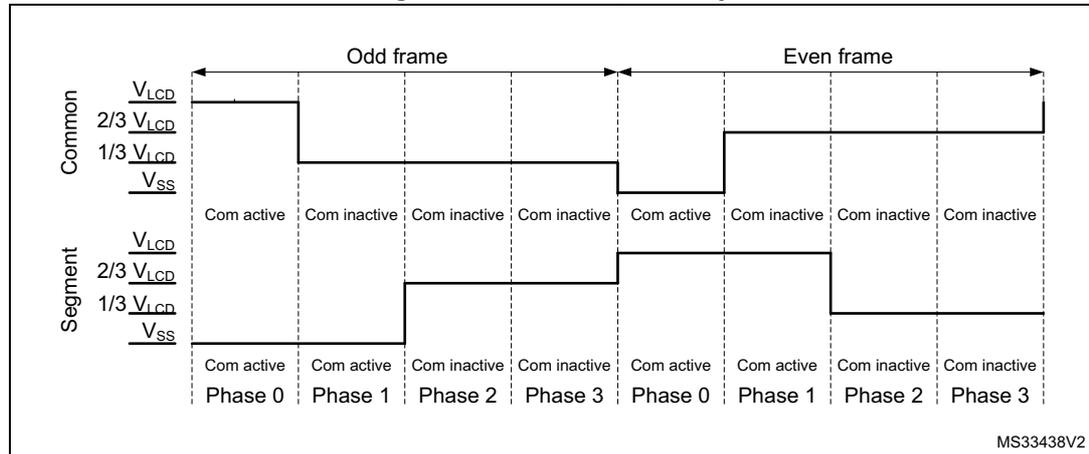
| Signal | Level | Phase | Odd frame | Even frame |
|---|---|---|---|---|
| Common | \( V_{\text{LCD}} \) | 0 | Com active | Com active |
| \( 2/3 V_{\text{LCD}} \) | 1 | Com inactive | Com active | |
| \( 1/3 V_{\text{LCD}} \) | 2 | Com inactive | Com inactive | |
| \( V_{\text{SS}} \) | 3 | Com inactive | Com inactive | |
| Segment | \( V_{\text{LCD}} \) | 0 | Com active | Com active |
| \( 2/3 V_{\text{LCD}} \) | 1 | Com active | Com active | |
| \( 1/3 V_{\text{LCD}} \) | 2 | Com inactive | Com inactive | |
| \( V_{\text{SS}} \) | 3 | Com inactive | Com inactive |
In case of 1/2 bias (BIAS = 01), the VLCD pin generates an intermediate voltage equal to \( 1/2 V_{\text{LCD}} \) on node b for odd and even frames (see Figure 138).
COM signal duty
Depending on DUTY[2:0] in LCD_CR, the COM signals are generated with static duty (see Figure 137), 1/2 duty (see Figure 138), 1/3 duty (see Figure 139), 1/4 duty (see Figure 140), or 1/8 duty (see Figure 141).
COM[n] n[0 to 7] is active during phase n in the odd frame, so the COM pin is driven to \( V_{LCD} \) .
During phase n of the even frame, the COM pin is driven to \( V_{SS} \) .
In the case of 1/3 or 1/4 bias, COM[n] is inactive during phases other than n, so the COM pin is driven to 1/3 (1/4) \( V_{LCD} \) during odd frames, and to 2/3 (3/4) \( V_{LCD} \) during even frames.
In the case of 1/2 bias, if COM[n] is inactive during phases other than n, the COM pin is always driven (odd and even frame) to 1/2 \( V_{LCD} \) .
When static duty is selected, the segment lines are not multiplexed, which means that each segment output corresponds to one pixel. In this way, only up to 44 pixels can be driven. COM[0] is always active while COM[7:1] are not used and are driven to \( V_{SS} \) .
When LCDEN in LCD_CR is reset, all common lines are pulled down to \( V_{SS} \) , and the ENS flag in LCD_SR becomes 0. Static duty means that COM[0] is always active, and only two voltage levels are used for segment and common lines: \( V_{LCD} \) and \( V_{SS} \) . A pixel is active if the corresponding SEG line has a voltage opposite to that of the COM, and inactive when the voltages are equal. In this way the LCD has maximum contrast (see Figure 136, Figure 137).
In the figure below, pixel 0 is active while pixel 1 is inactive.
Figure 136. Static duty case 1
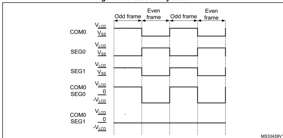
The diagram shows the voltage levels for COM0, SEG0, and SEG1 over four frames: Odd frame, Even frame, Odd frame, and Even frame. The vertical axis lists the signals and their possible voltage levels: \( V_{LCD} \) , \( V_{SS} \) , 0, and \( -V_{LCD} \) .
- COM0: In the first two rows, COM0 is shown with levels \( V_{LCD} \) and \( V_{SS} \) . It is at \( V_{LCD} \) during the first Odd frame and \( V_{SS} \) during the first Even frame, then repeats for the second Odd and Even frames.
- SEG0: In the next two rows, SEG0 is shown with levels \( V_{LCD} \) and \( V_{SS} \) . It is at \( V_{SS} \) during the first Odd frame and \( V_{LCD} \) during the first Even frame, then repeats for the second Odd and Even frames. This is the opposite of COM0.
- SEG1: In the next two rows, SEG1 is shown with levels \( V_{LCD} \) and \( V_{SS} \) . It is at \( V_{LCD} \) during the first Odd frame and \( V_{SS} \) during the first Even frame, then repeats for the second Odd and Even frames. This is the same as COM0.
- COM0 / SEG0: In the next two rows, COM0 and SEG0 are shown together with levels \( V_{LCD} \) , 0, and \( -V_{LCD} \) . COM0 is at \( V_{LCD} \) during the first Odd frame and \( V_{SS} \) during the first Even frame. SEG0 is at 0 during the first Odd frame and \( -V_{LCD} \) during the first Even frame.
- COM0 / SEG1: In the last two rows, COM0 and SEG1 are shown together with levels \( V_{LCD} \) , 0, and \( -V_{LCD} \) . COM0 is at \( V_{LCD} \) during the first Odd frame and \( V_{SS} \) during the first Even frame. SEG1 is at 0 during the first Odd frame and \( -V_{LCD} \) during the first Even frame.
The diagram illustrates that in this static duty case, COM0 is always active (driven to \( V_{LCD} \) in odd frames and \( V_{SS} \) in even frames), while SEG0 and SEG1 are inactive (driven to \( V_{SS} \) in odd frames and \( V_{LCD} \) in even frames). The voltage levels 0 and \( -V_{LCD} \) are also shown for SEG0 and SEG1.
In each frame, there is only one phase, this is why \( f_{frame} \) is equal to \( f_{LCD} \) . If 1/4 duty is selected there are four phases in a frame in which COM[0] is active during phase 0, COM[1] is active during phase 1, COM[2] is active during phase 2, and COM[3] is active during phase 3.
Figure 137. Static duty case 2
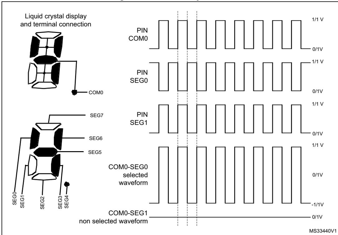
The figure illustrates the timing for a static duty case 2. On the left, a diagram shows the liquid crystal display and terminal connections. COM0 is connected to a common terminal. SEG7, SEG6, SEG5, SEG4, SEG3, SEG2, and SEG1 are connected to segment terminals. The right side shows timing waveforms over four phases (indicated by vertical dashed lines). The waveforms are:
- PIN COM0: A square wave alternating between 1/1 V and 0/1V.
- PIN SEG0: A square wave alternating between 1/1 V and 0/1V.
- PIN SEG1: A square wave alternating between 1/1 V and 0/1V.
- COM0-SEG0 selected waveform: A square wave alternating between 1/1 V and -1/1V.
- COM0-SEG1 non selected waveform: A constant line at 0/1V.
In this mode, the segment terminals are multiplexed, and each of them control four pixels. A pixel is activated only when both of its corresponding SEG and COM lines are active in the same phase. In case of 1/4 duty, to deactivate pixel 0 connected to COM[0], SEG[0] needs to be inactive during the phase 0 when COM[0] is active. To activate pixel 0 connected to COM[1], SEG[0] needs to be active during phase 1 when COM[1] is active (see Figure 140). To activate pixels from 0 to 43 connected to COM[0], SEG[0:43] needs to be active during phase 0 when COM[0] is active. These considerations can be extended to the other pixels.
Eight-to-one mux
When COM[0] is active the common driver block, it also drives the eight-to-one mux shown in Figure 134 in order to select the content of first two RAM register locations. When COM[7] is active, the output of the eight-to-one mux is the content of the last two RAM locations.
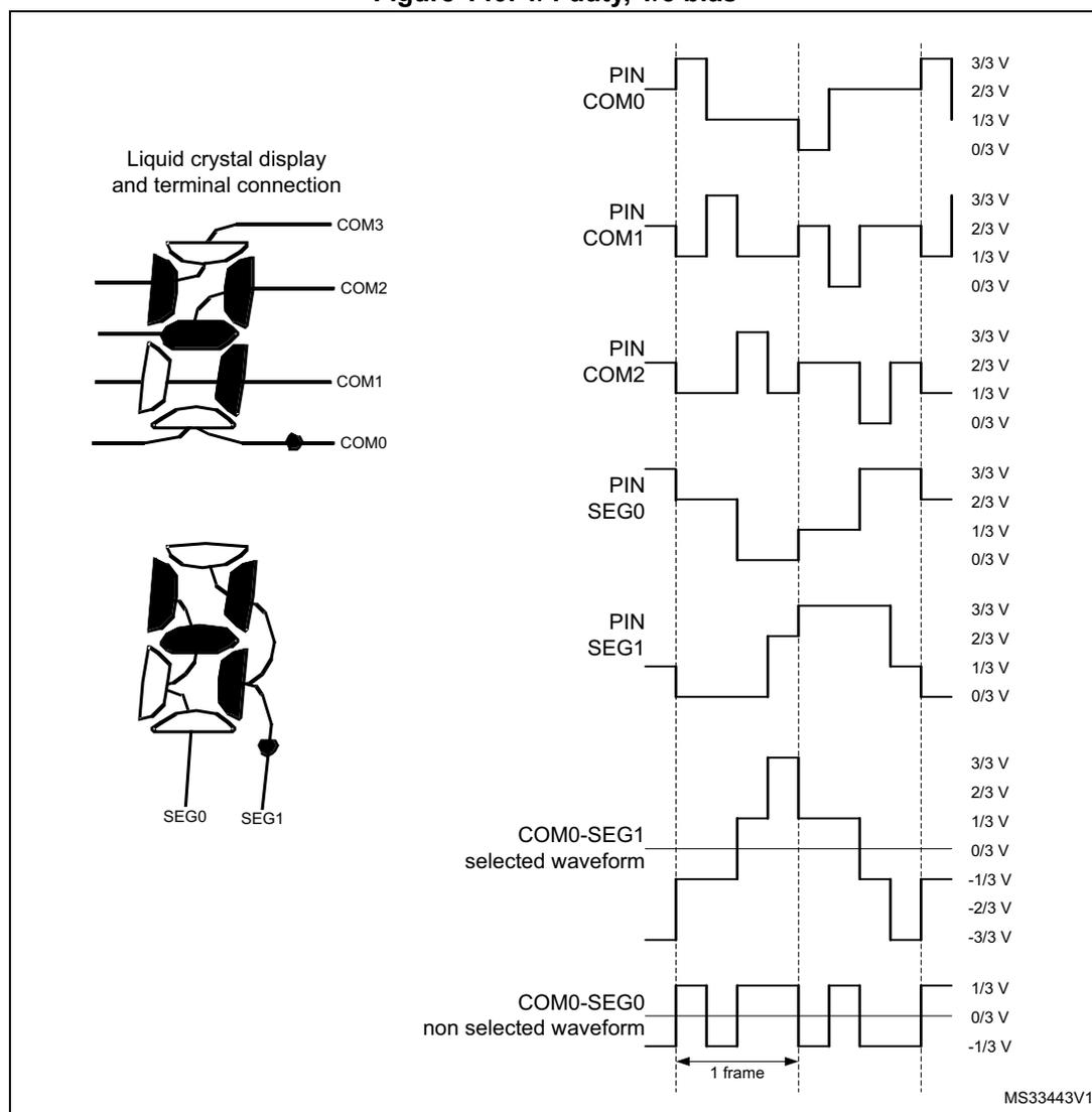
Figure 138. 1/2 duty, 1/2 bias
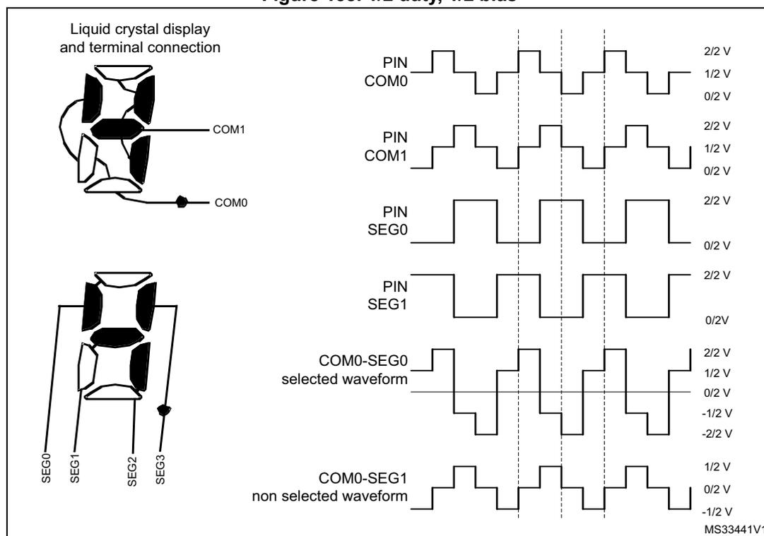
The figure illustrates the terminal connections and timing waveforms for a 1/2 duty, 1/2 bias LCD. On the left, a diagram shows a 4x4 grid of pixels with terminals COM1, COM0, SEG0, SEG1, SEG2, and SEG3. On the right, timing diagrams show the voltage levels for various pins and waveforms over time. The voltage levels are 2/2 V, 1/2 V, 0/2 V, and -1/2 V. The waveforms are labeled PIN COM0, PIN COM1, PIN SEG0, PIN SEG1, COM0-SEG0 selected waveform, and COM0-SEG1 non selected waveform. The selected waveform for COM0-SEG0 shows a voltage level of 2/2 V, while the non-selected waveform for COM0-SEG1 shows a voltage level of 1/2 V.
22.3.4 Segment driver
The segment driver block controls the SEG lines according to the pixel data coming from the eight-to-one mux driven in each phase by the common driver block.
In the case of 1/4 or 1/8 duty
When COM[0] is active, the pixel information (active/inactive) related to the pixel connected to COM[0] (content of the first two LCD_RAM locations) goes through the eight-to-one mux.
The SEG[n] pin \( n \) [0 to 43] is driven to \( V_{SS} \) (indicating pixel \( n \) is active when COM[0] is active) in phase 0 of the odd frame.
The SEG[n] pin is driven to \( V_{LCD} \) in phase 0 of the even frame. If pixel \( n \) is inactive then the SEG[n] pin is driven to \( 2/3 \) ( \( 2/4 \) ) \( V_{LCD} \) in the odd frame or \( 1/3 \) ( \( 2/4 \) ) \( V_{LCD} \) in the even frame (current inversion in \( V_{LCD} \) pad) (see Figure 135).
In case of 1/2 bias, if the pixel is inactive the SEG[n] pin is driven to \( V_{LCD} \) in the odd and to \( V_{SS} \) in the even frame.
When the LCD controller is disabled (LCDEN cleared in LCD_CR), then the SEG lines are pulled down to \( V_{SS} \) .
Figure 139. 1/3 duty, 1/3 bias
The figure illustrates the terminal connections and voltage waveforms for a liquid crystal display (LCD) controller operating in 1/3 duty and 1/3 bias mode. It is divided into two main sections: terminal connections and timing diagrams.
Liquid crystal display and terminal connection
The top diagram shows a 3-segment LCD with common terminals COM0, COM1, and COM2. The bottom diagram shows a 3-segment LCD with segment terminals SEG0, SEG1, and SEG2.
Timing Diagrams
The timing diagrams show the voltage levels for various pins over one frame. The vertical axis represents voltage levels: 3/3 V, 2/3 V, 1/3 V, 0/3 V, -1/3 V, -2/3 V, and -3/3 V. The horizontal axis represents time, with a "1 frame" duration indicated.
- PIN COM0: Square wave alternating between 3/3 V and 0/3 V.
- PIN COM1: Square wave alternating between 3/3 V and 0/3 V, phase-shifted from COM0.
- PIN COM2: Square wave alternating between 3/3 V and 0/3 V, phase-shifted from COM1.
- PIN SEG0: Square wave alternating between 3/3 V and 0/3 V.
- PIN SEG1: Constant 0/3 V.
- COM0-SEG1 selected waveform: Shows the voltage difference between COM0 and SEG1. It takes values of 3/3 V, 0/3 V, -1/3 V, -2/3 V, and -3/3 V.
- COM0-SEG0 non selected waveform: Shows the voltage difference between COM0 and SEG0. It takes values of 1/3 V, 0/3 V, and -1/3 V.
MS33442V1
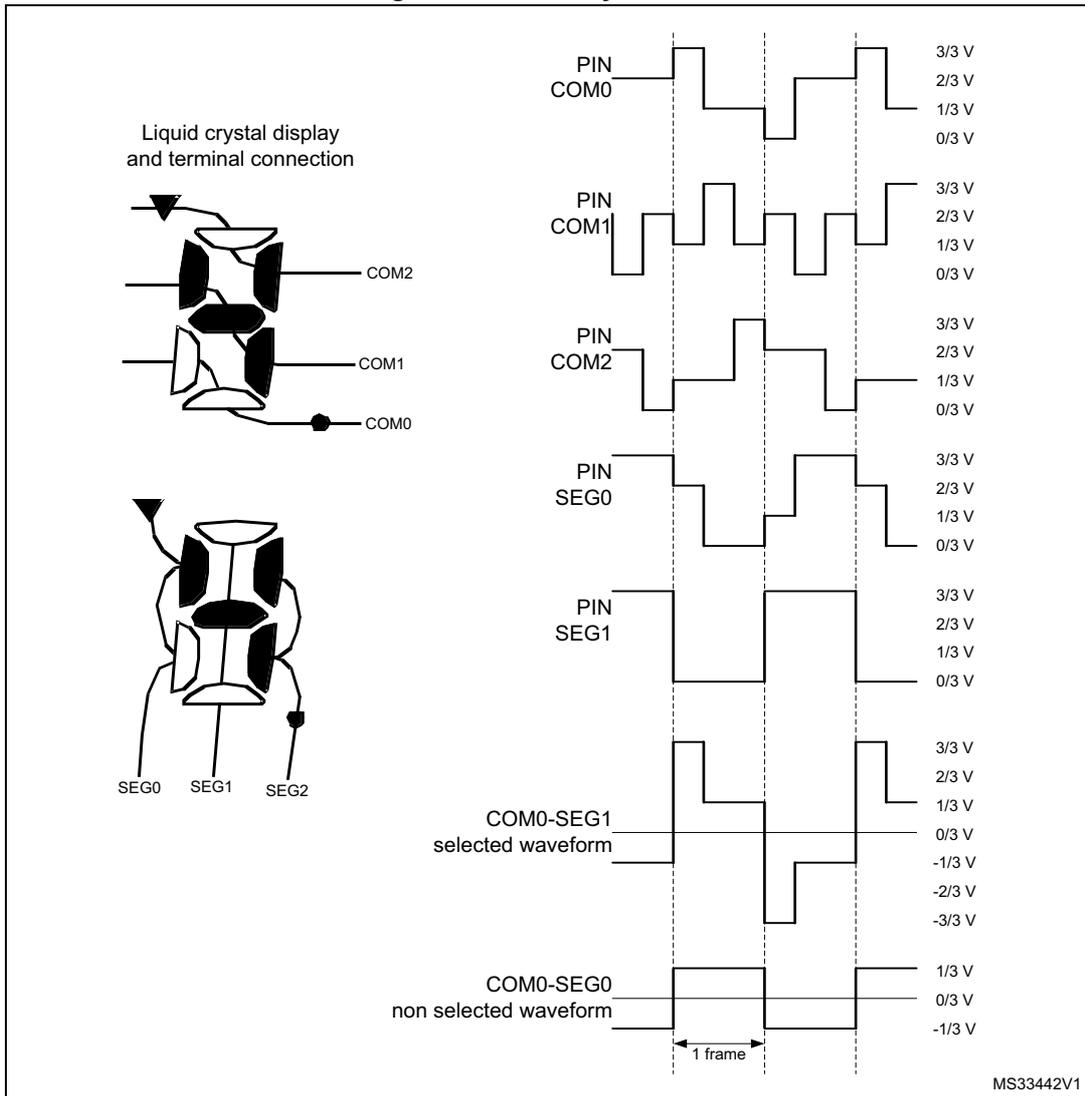
Figure 140. 1/4 duty, 1/3 bias
Liquid crystal display and terminal connection
The figure illustrates the terminal connections and voltage waveforms for a liquid crystal display (LCD) controller operating in 1/4 duty and 1/3 bias mode. On the left, a schematic shows the connection of four common terminals (COM0, COM1, COM2, COM3) and two segment terminals (SEG0, SEG1) to a grid of liquid crystal cells. On the right, timing diagrams show the voltage levels over time for these terminals. The common terminals (COM0, COM1, COM2, COM3) cycle through four voltage levels: 3/3 V, 2/3 V, 1/3 V, and 0/3 V. The segment terminals (SEG0, SEG1) cycle through three voltage levels: 3/3 V, 2/3 V, and 1/3 V. Below the terminal waveforms, two specific waveforms are shown: the 'COM0-SEG1 selected waveform' and the 'COM0-SEG0 non selected waveform'. The selected waveform has a peak-to-peak voltage of 3V (from -3/3 V to 3/3 V), while the non-selected waveform has a peak-to-peak voltage of 1V (from -1/3 V to 1/3 V). A '1 frame' duration is indicated on the time axis. The reference voltage levels for the waveforms are 3/3 V, 2/3 V, 1/3 V, 0/3 V, -1/3 V, -2/3 V, and -3/3 V.
PIN COM0
PIN COM1
PIN COM2
PIN SEG0
PIN SEG1
COM0-SEG1 selected waveform
COM0-SEG0 non selected waveform
1 frame
MS33443V1
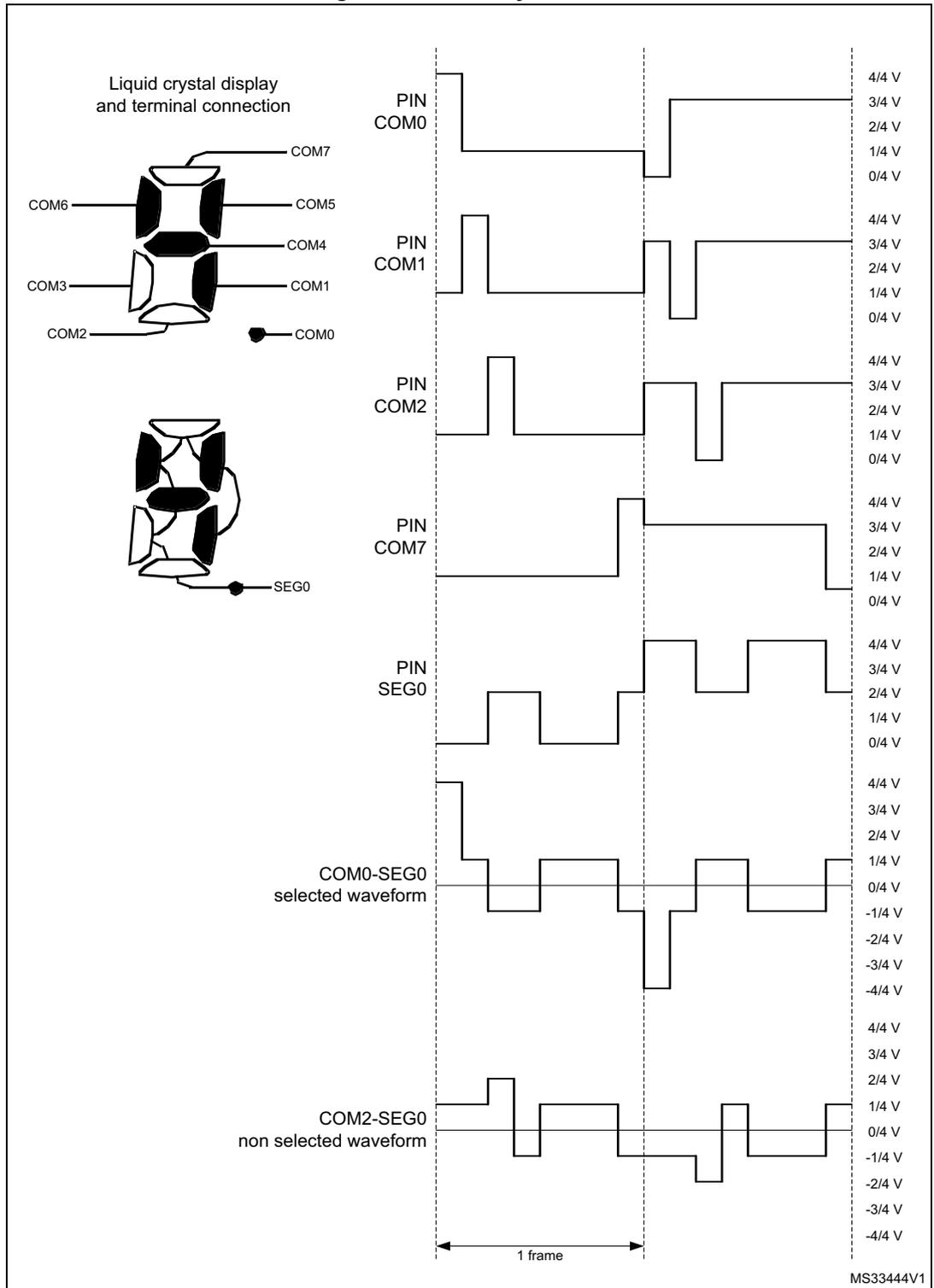
Figure 141. 1/8 duty, 1/4 bias
Liquid crystal display
and terminal connection
COM7
COM6
COM5
COM4
COM3
COM1
COM2
COM0
SEG0
PIN
COM0
PIN
COM1
PIN
COM2
PIN
COM7
PIN
SEG0
COM0-SEG0
selected waveform
COM2-SEG0
non selected waveform
4/4 V
3/4 V
2/4 V
1/4 V
0/4 V
4/4 V
3/4 V
2/4 V
1/4 V
0/4 V
4/4 V
3/4 V
2/4 V
1/4 V
0/4 V
4/4 V
3/4 V
2/4 V
1/4 V
0/4 V
4/4 V
3/4 V
2/4 V
1/4 V
0/4 V
4/4 V
3/4 V
2/4 V
1/4 V
0/4 V
-1/4 V
-2/4 V
-3/4 V
-4/4 V
1 frame
MS33444V1
Blink
The segment driver also implements a programmable blink feature to allow some pixels to continuously switch on at a specific frequency. The blink mode can be configured by BLINK[1:0] in LCD_FCR, making possible to blink up to 1, 2, 4, 8, or all pixels (see Section 22.6.2 ). The blink frequency can be selected from eight different values using BLINKF[2:0] in LCD_FCR.
The table below gives examples of different blink frequencies (as a function of ck_div frequency).
Table 110. Blink frequency
| BLINKF[2:0] | ck_div frequency (with LCDCLK frequency of 32.768 kHz) | |||||
|---|---|---|---|---|---|---|
| 32 Hz | 64 Hz | 128 Hz | 256 Hz | |||
| 0 | 0 | 0 | 4.0 Hz | N/A | N/A | N/A |
| 0 | 0 | 1 | 2.0 Hz | 4.0 Hz | N/A | N/A |
| 0 | 1 | 0 | 1.0 Hz | 2.0 Hz | 4.0 Hz | N/A |
| 0 | 1 | 1 | 0.5 Hz | 1.0 Hz | 2.0 Hz | 4.0 Hz |
| 1 | 0 | 0 | 0.25 Hz | 0.5 Hz | 1.0 Hz | 2.0 Hz |
| 1 | 0 | 1 | N/A | 0.25 Hz | 0.5 Hz | 1.0 Hz |
| 1 | 1 | 0 | N/A | N/A | 0.25 Hz | 0.5 Hz |
| 1 | 1 | 1 | N/A | N/A | N/A | 0.25 Hz |
22.3.5 Voltage generator and contrast control
LCD supply source
The LCD power supply source comes from either the internal stepup converter, or from an external voltage applied on the VLCD pin. The internal or external voltage source can be selected using VSEL in LCD_CR. In case of external source selected, the internal boost circuit (stepup converter) is disabled to reduce power consumption.
When the stepup converter is selected as \( V_{LCD} \) source, the \( V_{LCD} \) value can be chosen among a wide set of values from \( V_{LCDmin} \) to \( V_{LCDmax} \) by means of CC[2:0] (contrast control) in LCD_FCR (see Section 22.6.2 ). New values of \( V_{LCD} \) takes effect every beginning of a new frame.
When external power source is selected as \( V_{LCD} \) source, the \( V_{LCD} \) voltage must be chosen in the range of \( V_{LCDmin} \) to \( V_{LCDmax} \) (see datasheets). The contrast can then be controlled by programming a dead time between frames (see Deadtime ).
A specific software sequence must be performed to configure the LCD depending on the LCD power supply source to be used. The LCD controller is considered as disabled prior to the configuration sequence.
In case the internal stepup converter is used (capacitor \( C_{EXT} \) on VLCD pin is required):
- Configure the VLCD pin as alternate function LCD in the GPIO_AFR register.
- Wait for the external capacitor \( C_{EXT} \) to be charged ( \( C_{EXT} \) connected to the VLCD pin, approximately 2 ms for \( C_{EXT} = 1 \mu F \) )
- • Set voltage source to internal source by resetting VSEL in LCD_CR.
- • Enable the LCD controller by setting LCDEN in LCD_CR.
In case of LCD external power source is used:
- • Set voltage source to external source by setting VSEL in LCD_CR.
- • Configure the VLCD pin as alternate function LCD in GPIO_AFR.
- • Enable the LCD controller by setting LCDEN in LCD_CR.
LCD intermediate voltages
The LCD intermediate voltage levels are generated through an internal resistor divider network as shown in Figure 142 .
The LCD voltage generator issues intermediate voltage levels between \( V_{SS} \) and \( V_{LCD} \) :
- • \( 1/3 V_{LCD} \) and \( 2/3 V_{LCD} \) in case of 1/3 bias
- • \( 1/4 V_{LCD} \) , \( 2/4 V_{LCD} \) and \( 3/4 V_{LCD} \) in case of 1/4 bias
- • only \( 1/2 V_{LCD} \) in case of 1/2 bias.
LCD drive selection
Two resistive networks, one with low-value resistors ( \( R_L \) ), and one with high-value resistors ( \( R_H \) ) are respectively used to increase the current during transitions, and to reduce power consumption in static state.
The EN switch follows the rules described below (see Figure 142 ):
- • If LCDEN is set in LCD_CR, the EN switch is closed.
- • When clearing LCDEN in LCD_CR, the EN switch is open at the end of the even frame in order to avoid a medium voltage level different from 0 considering the entire frame odd plus even.
PON[2:0] (pulse on duration) in LCD_FCR configures the time during which \( R_L \) is enabled through the HD (high drive) switch when the levels of the common and segment lines change (see Figure 142 ). A short drive time leads to lower power consumption, but displays with high internal resistance may need a longer drive time to achieve satisfactory contrast.
Figure 142. LCD voltage control
![Figure 142. LCD voltage control circuit diagram. The diagram shows two resistor networks, R_LN (low value) and R_HN (high value), connected to V_LCD. The R_LN network consists of three stages: 3 R_L, R_L, and 2 R_L resistors in series, with taps at 3/4 x V_LCD, 2/3 x V_LCD, 1/2 x V_LCD, 1/3 x V_LCD, and 1/4 x V_LCD. The R_HN network consists of three stages: 3 R_H, R_H, and 2 R_H resistors in series, with taps at the same intermediate voltage levels. These intermediate voltages are connected to three buffered output stages (BUFEN) to produce V_LCDRail3, V_LCDRail2, and V_LCDRail1. A switch labeled HD controls the R_LN network, and a switch labeled EN controls the R_HN network. A STATIC input is connected to V_SS. A BIAS[1] input is connected to an inverter. The diagram is labeled MS33445V2.](/RM0394-STM32L41-42-43-44-45-46/95ab0a2a5313b14be1da0ac074da0b3f_img.jpg)
- 1. \( R_{LN} \) and \( R_{HN} \) are the low value resistance network and the high value resistance network, respectively.
The \( R_{LN} \) divider can be always switched on using HD in LCD_FCR (see Section 22.6.2 ).
The HD switch follows the rules described below:
- • If HD and PON[2:0] are reset in LCD_FCR, the HD switch is open.
- • If HD is reset in LCD_FCR, and PON[2:0] in LCD_FCR are different from 00, the HD switch is closed during the number of pulses defined in PON[2:0].
- • If HD = 1 in LCD_FCR, then HD switch is always closed.
After LCDEN is activated, RDY is set in LCD_SR to indicate that voltage levels are stable and the LCD controller can start to work.
Buffered mode
When voltage output buffers are enabled by setting BUFEN in LCD_CR, the LCD driving capability is improved as buffers prevent the LCD capacitive loads from loading the resistor bridge unacceptably and interfering with its voltage generation. As a result, intermediate voltage levels are more stable, which improves RMS voltage applied to the LCD pixels.
In buffer mode, intermediate voltages are generated by the high value resistor bridge \( R_{HN} \) to reduce power consumption. The low value resistor bridge \( R_{LN} \) is automatically disabled whatever HD or PON[2:0] configuration.
Buffers can be used independently of the \( V_{LCD} \) supply source (internal or external), but they can only be enabled or disabled when the LCD controller is not activated.
Deadtime
In addition to using CC[2:0], the contrast can be controlled by programming a dead time between each frame. During the dead time, the COM and SEG values are put to \( V_{SS} \) . DEAD[2:0] in LCD_FCR can be used to program a time of up to eight phase periods. This dead time reduces the contrast without modifying the frame rate.
Figure 143. Deadtime
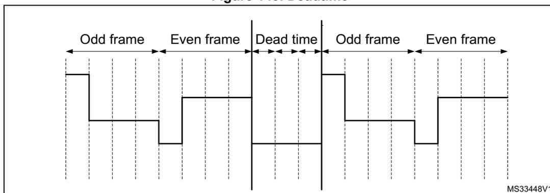
The diagram shows a timing sequence for LCD frames. It starts with an 'Odd frame', followed by an 'Even frame'. A 'Dead time' period follows, during which the signal levels drop to a lower level ( \( V_{SS} \) ). This is followed by another 'Odd frame' and 'Even frame'. Vertical dashed lines indicate the boundaries of the frames and the dead time period. The label 'MS33448V1' is present in the bottom right corner of the diagram area.
22.3.6 Double-buffer memory
Using its double-buffer memory, the LCD controller ensures the coherency of the displayed information without having to use interrupts to control the LCD_RAM modification.
The application software can access the first buffer level (LCD_RAM) through the APB interface. Once it has modified the LCD_RAM, it sets UDR in LCD_SR. This UDR flag (update display request) requests the updated information to be moved into the second buffer level (LCD_DISPLAY).
This operation is done synchronously with the frame (at the beginning of the next frame). Until the update is completed, the LCD_RAM is write protected, and the UDR flag stays high. Once the update is completed, another flag (UDD, update display done) is set and generates an interrupt if UDDIE is set in LCD_FCR.
The time it takes to update LCD_DISPLAY is, in the worst case, one odd and one even frame.
The update does not occur (UDR = 1 and UDD = 0) until the display is enabled (LCDEN = 1)
22.3.7 COM and SEG multiplexing
Output pins versus duty modes
The output pins consists of:
- • SEG[43:0]
- • COM[3:0]
Depending on the duty configuration, the COM and SEG output pins can have different functions:
- • In static, 1/2, 1/3, and 1/4 duty modes, there are up to 44 SEG pins and respectively 1, 2, 3, and 4 COM pins
- • In 1/8 duty mode (DUTY[2:0] = 100), COM[7:4] outputs are available on SEG[43:40] pins, reducing to the number of available segments to 40.
Remapping capability for small packages
Additionally, it is possible to remap four segments by setting MUX_SEG in LCD_CR. This is particularly useful when using smaller device types with fewer external pins.
When MUX_SEG is set, output pins SEG[43:40] have the same function as SEG[31:28].
This feature is available only if the mode 1/8 duty is not selected.
Check the availability of this feature by referring to the pinout section of the datasheet.
For the considered package, check the availability of the SEG/COM multiplexing pin as follow (n = number of segment for the considered package):
- • LCD_SEG[n-1]/LCD_COM7/LCD_SEG[31]
- • LCD_SEG[n-2]/LCD_COM6/LCD_SEG[30]
- • LCD_SEG[n-3]/LCD_COM5/LCD_SEG[29]
- • LCD_SEG[n-4]/LCD_COM4/LCD_SEG[28]
Summary of COM and SEG functions versus duty and remap
All the possible ways of multiplexing the COM and SEG functions are described in the table below.
Table 111. Remapping capability
| Configuration bits | SEG x COM | Output pin | Function | |
|---|---|---|---|---|
| DUTY | MUX_SEG | |||
| 1/8 | 0/1 | 40x8 | SEG[43:40]/SEG[31:28]/COM[7:4] | COM[7:4] |
| COM[3:0] | COM[3:0] | |||
| SEG[39:0] | SEG[39:0] | |||
| 0/1 | 28x8 | SEG[43:40]/SEG[31:28]/COM[7:4] | COM[7:4] | |
| COM[3:0] | COM[3:0] | |||
| SEG[27:0] | SEG[27:0] | |||
Table 111. Remapping capability (continued)
| Configuration bits | SEG x COM | Output pin | Function | |
|---|---|---|---|---|
| DUTY | MUX_SEG | |||
| 1/4 | 0 | 44x4 | COM[3:0] | COM[3:0] |
| SEG[43:40]/SEG[31:28]/COM[7:4] | SEG[43:40] | |||
| SEG[39:0] | SEG[39:0] | |||
| 1 | 40x4 | COM[3:0] | COM[3:0] | |
| SEG[43:40]/SEG[31:28]/COM[7:4] | SEG[31:28] | |||
| SEG[39:32] | SEG[39:32] | |||
| SEG[31:28] | not used | |||
| SEG[27:0] | SEG[27:0] | |||
| 0 | 28x4 | COM[3:0] | COM[3:0] | |
| SEG[43:40]/SEG[31:28]/COM[7:4] | not used | |||
| SEG[27:0] | SEG[27:0] | |||
| 1 | 32x4 | COM[3:0] | COM[3:0] | |
| SEG[43:40]/SEG[31:28]/COM[7:4] | SEG[31:28] | |||
| SEG[27:0] | SEG[27:0] | |||
| 1/3 | 0 | 44x3 | COM3 | not used |
| COM[2:0] | COM[2:0] | |||
| SEG[43:40]/SEG[31:28]/COM[7:4] | SEG[43:40] | |||
| SEG[39:0] | SEG[39:0] | |||
| 1 | 40x3 | COM3 | not used | |
| COM[2:0] | COM[2:0] | |||
| SEG[43:40]/SEG[31:28]/COM[7:4] | SEG[31:28] | |||
| SEG[39:32] | SEG[39:32] | |||
| SEG[31:28] | not used | |||
| 0 | 28x3 | SEG[27:0] | SEG[27:0] | |
| COM3 | not used | |||
| COM[2:0] | COM[2:0] | |||
| SEG[43:40]/SEG[31:28]/COM[7:4] | not used | |||
| 1 | 32x3 | SEG[31:0] | SEG[31:0] | |
| COM3 | not used | |||
| COM[2:0] | COM[2:0] | |||
| SEG[43:40]/SEG[31:28]/COM[7:4] | SEG[31:28] | |||
| SEG[27:0] | SEG[27:0] | |||
Table 111. Remapping capability (continued)
| Configuration bits | SEG x COM | Output pin | Function | |
|---|---|---|---|---|
| DUTY | MUX_SEG | |||
| 1/2 | 0 | 44x2 | COM[3:2] | not used |
| COM[1:0] | COM[1:0] | |||
| SEG[43:40]/SEG[31:28]/COM[7:4] | SEG[43:40] | |||
| SEG[39:0] | SEG[39:0] | |||
| 1 | 40x2 | COM[3:2] | not used | |
| COM[1:0] | COM[1:0] | |||
| SEG[43:40]/SEG[31:28]/COM[7:4] | SEG[31:28] | |||
| SEG[39:32] | SEG[39:32] | |||
| 1/2 | 0 | 28x2 | SEG[31:28] | not used |
| SEG[27:0] | SEG[27:0] | |||
| COM[3:2] | not used | |||
| COM[1:0] | COM[1:0] | |||
| 1 | 32x2 | SEG[43:40]/SEG[31:28]/COM[7:4] | SEG[31:28] | |
| SEG[27:0] | SEG[27:0] | |||
Table 111. Remapping capability (continued)
| Configuration bits | SEG x COM | Output pin | Function | |
|---|---|---|---|---|
| DUTY | MUX_SEG | |||
| STATIC | 0 | 44x1 | COM[3:1] | not used |
| COM0 | COM0 | |||
| SEG[43:40]/SEG[31:28]/COM[7:4] | SEG[43:40] | |||
| SEG[39:0] | SEG[39:0] | |||
| 1 | 40x1 | COM[3:1] | not used | |
| COM0 | COM0 | |||
| SEG[43:40]/SEG[31:28]/COM[7:4] | SEG[31:28] | |||
| SEG[39:32] | SEG[39:32] | |||
| SEG[31:28] | not used | |||
| SEG[27:0] | SEG[27:0] | |||
| 0 | 28x1 | COM[3:1] | not used | |
| COM0 | COM0 | |||
| SEG[43:40]/SEG[31:28]/COM[7:4] | not used | |||
| SEG[27:0] | SEG[27:0] | |||
| 1 | 32x1 | COM[3:1] | not used | |
| COM0 | COM0 | |||
| SEG[43:40]/SEG[31:28]/COM[7:4] | SEG[31:28] | |||
| SEG[27:0] | SEG[27:0] | |||
The figure below gives examples showing the signal connections to the external pins.
Figure 144. SEG/COM mux feature example
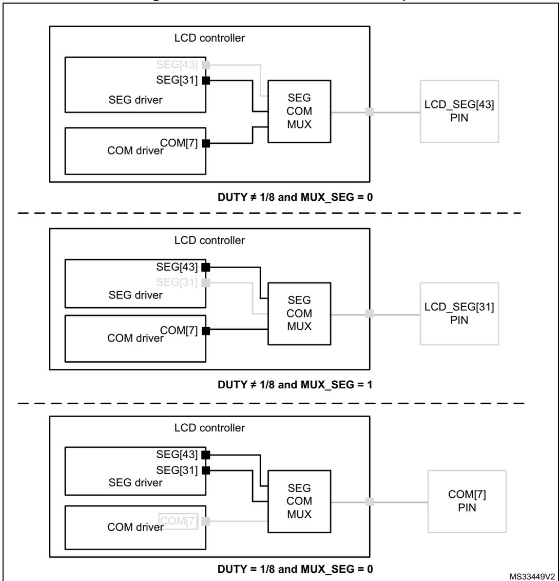
The figure illustrates three examples of signal connections to external pins for an LCD controller, separated by dashed lines. Each example shows the internal components of the LCD controller: a SEG driver, a COM driver, and a SEG COM MUX.
- Top Example: Labeled DUTY ≠ 1/8 and MUX_SEG = 0 . The SEG driver's output for SEG[43] is connected to the SEG COM MUX, which is then connected to the external pin LCD_SEG[43] PIN . The COM driver's output for COM[7] is also connected to the SEG COM MUX but is not connected to an external pin.
- Middle Example: Labeled DUTY ≠ 1/8 and MUX_SEG = 1 . The SEG driver's output for SEG[31] is connected to the SEG COM MUX, which is then connected to the external pin LCD_SEG[31] PIN . The COM driver's output for COM[7] is also connected to the SEG COM MUX but is not connected to an external pin.
- Bottom Example: Labeled DUTY = 1/8 and MUX_SEG = 0 . The COM driver's output for COM[7] is connected to the SEG COM MUX, which is then connected to the external pin COM[7] PIN . The SEG driver's outputs for SEG[43] and SEG[31] are also connected to the SEG COM MUX but are not connected to external pins.
MS33449V2
22.3.8 Flowchart
Figure 145. Flowchart example
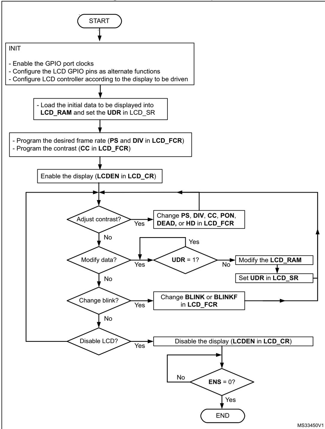
graph TD; START([START]) --> INIT["INIT<br/>- Enable the GPIO port clocks<br/>- Configure the LCD GPIO pins as alternate functions<br/>- Configure LCD controller according to the display to be driven"]; INIT --> LoadData["- Load the initial data to be displayed into<br/>LCD_RAM and set the UDR in LCD_SR"]; LoadData --> ProgramFCR["- Program the desired frame rate (PS and DIV in LCD_FCR)<br/>- Program the contrast (CC in LCD_FCR)"]; ProgramFCR --> EnableDisplay["Enable the display (LCDEN in LCD_CR)"]; EnableDisplay --> AdjustContrast{Adjust contrast?}; AdjustContrast -- Yes --> ChangeFCR["Change PS, DIV, CC, PON,<br/>DEAD, or HD in LCD_FCR"]; AdjustContrast -- No --> ModifyData{Modify data?}; ChangeFCR --> ModifyData; ModifyData -- Yes --> UDR1{UDR = 1?}; UDR1 -- Yes --> AdjustContrast; UDR1 -- No --> ModifyRAM["Modify the LCD_RAM"]; ModifyRAM --> SetUDR["Set UDR in LCD_SR"]; SetUDR --> ChangeBlink{Change blink?}; ChangeBlink -- Yes --> ChangeBlinkFCR["Change BLINK or BLINKF<br/>in LCD_FCR"]; ChangeBlinkFCR --> ChangeBlink; ChangeBlink -- No --> DisableLCD{Disable LCD?}; DisableLCD -- Yes --> DisableDisplay["Disable the display (LCDEN in LCD_CR)"]; DisableDisplay --> ENS0{ENS = 0?}; ENS0 -- No --> DisableDisplay; ENS0 -- Yes --> END([END]);MS33450V1
22.4 LCD low-power modes
The LCD controller can be displayed in Stop mode, or can be fully disabled to reduce power consumption.
Table 112. LCD behavior in low-power modes
| Mode | Description |
|---|---|
| Sleep | No effect. LCD interrupt causes the device to exit Sleep mode. |
| Low-power Run | No effect |
| Low-power Sleep | No effect. LCD interrupt causes the device to exit Low-power Sleep mode. |
| Stop 0 | No effect. LCD interrupt causes the device to exit Stop mode. |
| Stop 1 | |
| Stop 2 | |
| Standby | The LCD is powered down and must be reinitialized after exiting Standby or Shutdown mode. |
| Shutdown |
22.5 LCD interrupts
The table below gives the list of LCD interrupt requests.
Table 113. LCD interrupt requests
| Interrupt event | Event flag | Event flag Interrupt clearing method | Interrupt enable control bit |
|---|---|---|---|
| Start of frame (SOF) | SOF | Write SOFC = 1 | SOFIE |
| Update display done (UDD) | UDD | Write UDDC = 1 | UDDIE |
Start of frame (SOF)
The LCD start of frame interrupt is executed if SOFIE (start of frame interrupt enable) is set in LCD_FCR. SOF is cleared by writing SOFC to 1 in LCD_CLR when executing the corresponding interrupt handling vector.
Update display done (UDD)
The LCD update display interrupt is executed if UDDIE (update display done interrupt enable) is set in LCD_FCR. UDD is cleared by writing the UDDC to 1 in LCD_CLR when executing the corresponding interrupt handling vector.
Depending on the product implementation, all these interrupts events can either share the same interrupt vector (LCD global interrupt), or be grouped into two interrupt vectors (LCD SOF interrupt and LCD UDD interrupt). Refer to the Table 51: STM32L41xxx/42xxx/43xxx/44xxx/45xxx/46xxx vector table for details.
To enable the LCD interrupts, the following sequence is required:
- 1. Configure and enable the LCD IRQ channel in the NVIC.
- 2. Configure the LCD to generate interrupts.
22.6 LCD registers
These registers are accessed by words (32-bit).
22.6.1 LCD control register (LCD_CR)
Address offset: 0x00
Reset value: 0x0000 0000
VSEL, MUX_SEG, BIAS, DUTY, and BUFEN bitfields are write-protected when the LCD is enabled (ENS =1 in LCD_SR).
| 31 | 30 | 29 | 28 | 27 | 26 | 25 | 24 | 23 | 22 | 21 | 20 | 19 | 18 | 17 | 16 |
|---|---|---|---|---|---|---|---|---|---|---|---|---|---|---|---|
| Res. | Res. | Res. | Res. | Res. | Res. | Res. | Res. | Res. | Res. | Res. | Res. | Res. | Res. | Res. | Res. |
| 15 | 14 | 13 | 12 | 11 | 10 | 9 | 8 | 7 | 6 | 5 | 4 | 3 | 2 | 1 | 0 |
| Res. | Res. | Res. | Res. | Res. | Res. | Res. | BUFEN | MUX_S EG | BIAS[1:0] | DUTY[2:0] | VSEL | LCDEN | rw | ||
| rw | rw | rw | rw | ||||||||||||
Bits 31:9 Reserved, must be kept at reset value.
Bit 8 BUFEN : Voltage output buffer enable
This bit is used to enable/disable the voltage output buffer for higher driving capability.
0: Output buffer disabled
1: Output buffer enabled
Bit 7 MUX_SEG : Mux segment enable
This bit is used to enable SEG pin remapping. Four SEG pins can be multiplexed with SEG[31:28]. See Section 22.3.7 .
0: SEG pin multiplexing disabled
1: SEG[31:28] multiplexed with SEG[43:40]
Bits 6:5 BIAS[1:0] : Bias selector
These bits determine the bias used. Value 11 is forbidden.
00: Bias 1/4
01: Bias 1/2
10: Bias 1/3
11: Reserved
Bits 4:2 DUTY[2:0] : Duty selection
These bits determine the duty cycle. Values 101, 110 and 111 are forbidden.
000: Static duty
001: 1/2 duty
010: 1/3 duty
011: 1/4 duty
100: 1/8 duty
Others: Reserved
Bit 1 VSEL : Voltage source selection
This bit determines the voltage source for the LCD.
0: Internal source (voltage stepup converter)
1: External source (VLCD pin)
Bit 0 LCDEN : LCD controller enable
This bit is set by software to enable the LCD controller/driver. It is cleared by software to turn off the LCD at the beginning of the next frame. When the LCD is disabled, all COM and SEG pins are driven to \( V_{SS} \) .
0: LCD controller disabled
1: LCD controller enabled
22.6.2 LCD frame control register (LCD_FCR)
Address offset: 0x04
Reset value: 0x0000 0000
This register can be updated any time, but the new values are applied only at the beginning of the next frame (except for UDDIE, SOFIE that affect the device behavior immediately). The new value of CC[2:0] is also applied immediately, but its effect on the device is delayed at the beginning of the next frame by the voltage generator.
Reading this register gives the last value written in the register, and not the configuration used to display the current frame.
When BUFEN is set in LCD_CR, the low resistor divider network is automatically disabled whatever HD or PON[2:0] configuration.
| 31 | 30 | 29 | 28 | 27 | 26 | 25 | 24 | 23 | 22 | 21 | 20 | 19 | 18 | 17 | 16 |
|---|---|---|---|---|---|---|---|---|---|---|---|---|---|---|---|
| Res. | Res. | Res. | Res. | Res. | Res. | PS[3:0] | DIV[3:0] | BLINK[1:0] | |||||||
| rw | rw | rw | rw | rw | rw | rw | rw | rw | rw | ||||||
| 15 | 14 | 13 | 12 | 11 | 10 | 9 | 8 | 7 | 6 | 5 | 4 | 3 | 2 | 1 | 0 |
| BLINKF[2:0] | CC[2:0] | DEAD[2:0] | PON[2:0] | UDDIE | Res. | SOFIE | HD | ||||||||
| rw | rw | rw | rw | rw | rw | rw | rw | rw | rw | rw | rw | rw | rw | rw | |
Bits 31:26 Reserved, must be kept at reset value.
Bits 25:22 PS[3:0] : PS 16-bit prescaler
These bits are written by software to define the division factor of the PS 16-bit prescaler.
\( ck\_ps = LCDCLK/(2^{PS[3:0]}) \) . See Section 22.3.2 .
0000: \( ck\_ps = LCDCLK \)
0001: \( ck\_ps = LCDCLK/2 \)
0002: \( ck\_ps = LCDCLK/4 \)
...
1111: \( ck\_ps = LCDCLK/32768 \)
Bits 21:18 DIV[3:0] : DIV clock divider
These bits are written by software to define the division factor of the DIV divider (see Section 22.3.2 .)
0000: \( ck\_div = ck\_ps/16 \)
0001: \( ck\_div = ck\_ps/17 \)
0002: \( ck\_div = ck\_ps/18 \)
...
1111: \( ck\_div = ck\_ps/31 \)
Bits 17:16 BLINK[1:0] : Blink mode selection
- 00: Blink disabled
- 01: Blink enabled on SEG[0], COM[0] (1 pixel)
- 10: Blink enabled on SEG[0], all COMs (up to 8 pixels depending on the programmed duty)
- 11: Blink enabled on all SEGs and all COMs (all pixels)
Bits 15:13 BLINKF[2:0] : Blink frequency selection
- 000: \( f_{LCD}/8 \)
- 001: \( f_{LCD}/16 \)
- 010: \( f_{LCD}/32 \)
- 011: \( f_{LCD}/64 \)
- 100: \( f_{LCD}/128 \)
- 101: \( f_{LCD}/256 \)
- 110: \( f_{LCD}/512 \)
- 111: \( f_{LCD}/1024 \)
Bits 12:10 CC[2:0] : Contrast control
These bits specify one of the \( V_{LCD} \) maximum voltages (independent of \( V_{DD} \) ). It ranges from 2.60 V to 3.51V.
- 000: \( V_{LCD0} \)
- 001: \( V_{LCD1} \)
- 010: \( V_{LCD2} \)
- 011: \( V_{LCD3} \)
- 100: \( V_{LCD4} \)
- 101: \( V_{LCD5} \)
- 110: \( V_{LCD6} \)
- 111: \( V_{LCD7} \)
Note: Refer to the datasheet for the \( V_{LCDx} \) values.
Bits 9:7 DEAD[2:0] : Dead time duration
These bits are written by software to configure the length of the dead time between frames. During the dead time the COM and SEG voltage levels are held at 0 V to reduce the contrast without modifying the frame rate.
- 000: No dead time
- 001: 1 phase period dead time
- 010: 2 phase period dead time
- .....
- 111: 7 phase period dead time
These bits are written by software to define the pulse duration in terms of ck_ps pulses.
A short pulse leads to lower power consumption, but displays with high internal resistance may need a longer pulse to achieve satisfactory contrast.
Note that the pulse is never longer than one half prescaled LCD clock period.
000: 0
001: 1/ck_ps
010: 2/ck_ps
011: 3/ck_ps
100: 4/ck_ps
101: 5/ck_ps
110: 6/ck_ps
111: 7/ck_ps
PON duration example with LCDCLK = 32.768 kHz and PS=0x03:
000: 0 µs
001: 244 µs
010: 488 µs
011: 782 µs
100: 976 µs
101: 1.22 ms
110: 1.46 ms
111: 1.71 ms
Bit 3 UDDIE : Update display done interrupt enableThis bit is set and cleared by software.
0: LCD update display done interrupt disabled
1: LCD update display done interrupt enabled
Bit 2 Reserved, must be kept at reset value.
Bit 1 SOFIE : Start of frame interrupt enableThis bit is set and cleared by software.
0: LCD start-of-frame interrupt disabled
1: LCD start-of-frame interrupt enabled
Bit 0 HD : High drive enableThis bit is written by software to enable a low resistance divider. Displays with high internal resistance may need a longer drive time to achieve satisfactory contrast. This bit is useful in this case if some additional power consumption can be tolerated.
0: Permanent high drive disabled
1: Permanent high drive enabled. When HD = 1, PON[2:0] must be programmed to 001.
22.6.3 LCD status register (LCD_SR)
Address offset: 0x08
Reset value: 0x0000 0020
| 31 | 30 | 29 | 28 | 27 | 26 | 25 | 24 | 23 | 22 | 21 | 20 | 19 | 18 | 17 | 16 |
|---|---|---|---|---|---|---|---|---|---|---|---|---|---|---|---|
| Res. | Res. | Res. | Res. | Res. | Res. | Res. | Res. | Res. | Res. | Res. | Res. | Res. | Res. | Res. | Res. |
| 15 | 14 | 13 | 12 | 11 | 10 | 9 | 8 | 7 | 6 | 5 | 4 | 3 | 2 | 1 | 0 |
| Res. | Res. | Res. | Res. | Res. | Res. | Res. | Res. | Res. | Res. | FCRSF | RDY | UDD | UDR | SOF | ENS |
| r | r | r | rs | r | r |
Bits 31:6 Reserved, must be kept at reset value.
Bit 5 FCRSF : LCD frame control register synchronization flag
This bit is set by hardware each time the LCD_FCR register is updated in the LCDCLK domain. It is cleared by hardware when writing to the LCD_FCR register.
0: LCD frame control register not yet synchronized
1: LCD frame control register synchronized
Bit 4 RDY : Ready flag
This bit is set and cleared by hardware. It indicates the status of the stepup converter.
0: Not ready
1: Stepup converter enabled and ready to provide the correct voltage
Bit 3 UDD : Update display done
This bit is set by hardware. It is cleared by writing 1 to UDDC in LCD_CLR. The bit set has priority over the clear.
0: No event
1: Update display request done. A UDD interrupt is generated if UDDIE = 1 in LCD_FCR.
Note: If the device is in Stop mode (PCLK not provided), UDD does not generate an interrupt even if UDDIE = 1. If the display is not enabled, the UDD interrupt never occurs.
Bit 2 UDR : Update display request
Each time software modifies the LCD_RAM, it must set this bit to transfer the updated data to the second level buffer. This bit stays set until the end of the update. During this time, the LCD_RAM is write protected.
0: No effect
1: Update display request
Note: When the display is disabled, the update is performed for all LCD_DISPLAY locations. When the display is enabled, the update is performed only for locations for which commons are active (depending on DUTY). For example if DUTY = 1/2, only the LCD_DISPLAY of COM0 and COM1 are updated.
Writing 0 on this bit or writing 1 when it is already 1 has no effect. This bit can be cleared by hardware only. It can be cleared only when LCDEN = 1
Bit 1 SOF : Start-of-frame flag
This bit is set by hardware at the beginning of a new frame, at the same time as the display data is updated. It is cleared by writing a 1 to SOFC in LCD_CLR. The bit clear has priority over the set.
0: No event
1: Start-of-frame event occurred. An LCD SOF interrupt is generated if SOFIE is set.
Bit 0 ENS : LCD enabled status
This bit is set and cleared by hardware. It indicates the LCD controller status.
0: LCD controller disabled
1: LCD controller enabled
Note: This bit is set immediately when LCDEN in LCD_CR goes from 0 to 1. On deactivation, it reflects the real LCD status. It becomes 0 at the end of the last displayed frame.
22.6.4 LCD clear register (LCD_CLR)
Address offset: 0x0C
Reset value: 0x0000 0000
| 31 | 30 | 29 | 28 | 27 | 26 | 25 | 24 | 23 | 22 | 21 | 20 | 19 | 18 | 17 | 16 |
|---|---|---|---|---|---|---|---|---|---|---|---|---|---|---|---|
| Res. | Res. | Res. | Res. | Res. | Res. | Res. | Res. | Res. | Res. | Res. | Res. | Res. | Res. | Res. | Res. |
| 15 | 14 | 13 | 12 | 11 | 10 | 9 | 8 | 7 | 6 | 5 | 4 | 3 | 2 | 1 | 0 |
| Res. | Res. | Res. | Res. | Res. | Res. | Res. | Res. | Res. | Res. | Res. | Res. | UDDC | Res. | SOFC | Res. |
| w | w |
Bits 31:4 Reserved, must be kept at reset value.
Bit 3 UDDC : Update display done clear
This bit is written by software to clear UDD in LCD_SR.
0: No effect
1: Clear UDD flag.
Bit 2 Reserved, must be kept at reset value.
Bit 1 SOFC : Start-of-frame flag clear
This bit is written by software to clear SOF in LCD_SR.
0: No effect
1: Clear SOF flag.
Bit 0 Reserved, must be kept at reset value.
22.6.5 LCD display memory (LCD_RAMx)
Address offset: 0x14 + 0x4 * x, (x = 0, 2, 4, 6, 8, 10, 12, 14)
Reset value: 0x0000 0000
| 31 | 30 | 29 | 28 | 27 | 26 | 25 | 24 | 23 | 22 | 21 | 20 | 19 | 18 | 17 | 16 |
|---|---|---|---|---|---|---|---|---|---|---|---|---|---|---|---|
| SEGMENT_DATA[31:16] | |||||||||||||||
| rw | rw | rw | rw | rw | rw | rw | rw | rw | rw | rw | rw | rw | rw | rw | rw |
| 15 | 14 | 13 | 12 | 11 | 10 | 9 | 8 | 7 | 6 | 5 | 4 | 3 | 2 | 1 | 0 |
| SEGMENT_DATA[15:0] | |||||||||||||||
| rw | rw | rw | rw | rw | rw | rw | rw | rw | rw | rw | rw | rw | rw | rw | rw |
Bits 31:0 SEGMENT_DATA[31:0] :
Each bit corresponds to one pixel of the LCD display.
0: Pixel inactive
1: Pixel active
22.6.6 LCD display memory (LCD_RAMx)
Address offset: \( 0x14 + 0x4 * x \) , ( \( x = 1, 3, 5, 7 \) )
Reset value: 0x0000 0000
| 31 | 30 | 29 | 28 | 27 | 26 | 25 | 24 | 23 | 22 | 21 | 20 | 19 | 18 | 17 | 16 |
|---|---|---|---|---|---|---|---|---|---|---|---|---|---|---|---|
| Res. | Res. | Res. | Res. | Res. | Res. | Res. | Res. | Res. | Res. | Res. | Res. | Res. | Res. | Res. | Res. |
| 15 | 14 | 13 | 12 | 11 | 10 | 9 | 8 | 7 | 6 | 5 | 4 | 3 | 2 | 1 | 0 |
| Res. | Res. | Res. | Res. | SEGMENT_DATA[43:32] | |||||||||||
| rw | rw | rw | rw | rw | rw | rw | rw | rw | rw | rw | rw | ||||
Bits 31:12 Reserved, must be kept at reset value.
Bits 11:0 SEGMENT_DATA[43:32] :
Each bit corresponds to one pixel of the LCD display.
0: Pixel inactive
1: Pixel active
22.6.7 LCD display memory (LCD_RAMx)
Address offset: \( 0x14 + 0x4 * x \) , ( \( x = 9, 11, 13, 15 \) )
Reset value: 0x0000 0000
| 31 | 30 | 29 | 28 | 27 | 26 | 25 | 24 | 23 | 22 | 21 | 20 | 19 | 18 | 17 | 16 |
|---|---|---|---|---|---|---|---|---|---|---|---|---|---|---|---|
| Res. | Res. | Res. | Res. | Res. | Res. | Res. | Res. | Res. | Res. | Res. | Res. | Res. | Res. | Res. | Res. |
| 15 | 14 | 13 | 12 | 11 | 10 | 9 | 8 | 7 | 6 | 5 | 4 | 3 | 2 | 1 | 0 |
| Res. | Res. | Res. | Res. | Res. | Res. | Res. | Res. | SEGMENT_DATA[39:32] | |||||||
| rw | rw | rw | rw | rw | rw | rw | rw | ||||||||
Bits 31:8 Reserved, must be kept at reset value.
Bits 7:0 SEGMENT_DATA[39:32] :
Each bit corresponds to one pixel of the LCD display.
0: Pixel inactive
1: Pixel active
22.6.8 LCD register map
Table 114. LCD register map and reset values
| Offset | Register name | 31 | 30 | 29 | 28 | 27 | 26 | 25 | 24 | 23 | 22 | 21 | 20 | 19 | 18 | 17 | 16 | 15 | 14 | 13 | 12 | 11 | 10 | 9 | 8 | 7 | 6 | 5 | 4 | 3 | 2 | 1 | 0 |
|---|---|---|---|---|---|---|---|---|---|---|---|---|---|---|---|---|---|---|---|---|---|---|---|---|---|---|---|---|---|---|---|---|---|
| 0x00 | LCD_CR | Res. | Res. | Res. | Res. | Res. | Res. | Res. | Res. | Res. | Res. | Res. | Res. | Res. | Res. | Res. | Res. | Res. | Res. | Res. | Res. | Res. | Res. | Res. | BufEN | Mux_SEG | BIAS[1:0] | DUTY [2:0] | VSEL | LCDEN | |||
| Reset value | 0 | 0 | 0 | 0 | 0 | 0 | 0 | 0 | |||||||||||||||||||||||||
Table 114. LCD register map and reset values (continued)
| Offset | Register name | 31 | 30 | 29 | 28 | 27 | 26 | 25 | 24 | 23 | 22 | 21 | 20 | 19 | 18 | 17 | 16 | 15 | 14 | 13 | 12 | 11 | 10 | 9 | 8 | 7 | 6 | 5 | 4 | 3 | 2 | 1 | 0 |
|---|---|---|---|---|---|---|---|---|---|---|---|---|---|---|---|---|---|---|---|---|---|---|---|---|---|---|---|---|---|---|---|---|---|
| 0x04 | LCD_FCR | Res. | Res. | Res. | Res. | Res. | Res. | PS[3:0] | DIV[3:0] | BLINK[1:0] | BLINKF [2:0] | CC[2:0] | DEAD [2:0] | PON [2:0] | UDDIE | Res. | SOFIE | HD | |||||||||||||||
| Reset value | 0 | 0 | 0 | 0 | 0 | 0 | 0 | 0 | 0 | 0 | 0 | 0 | 0 | 0 | 0 | 0 | 0 | 0 | 0 | 0 | 0 | 0 | 0 | 0 | 0 | ||||||||
| 0x08 | LCD_SR | Res. | Res. | Res. | Res. | Res. | Res. | Res. | Res. | Res. | Res. | Res. | Res. | Res. | Res. | Res. | Res. | Res. | Res. | Res. | Res. | Res. | Res. | Res. | Res. | Res. | Res. | FCRSF | RDY | UDD | UDR | SOF | ENS |
| Reset value | 1 | 0 | 0 | 0 | 0 | 0 | |||||||||||||||||||||||||||
| 0x0C | LCD_CLR | Res. | Res. | Res. | Res. | Res. | Res. | Res. | Res. | Res. | Res. | Res. | Res. | Res. | Res. | Res. | Res. | Res. | Res. | Res. | Res. | Res. | Res. | Res. | Res. | Res. | Res. | Res. | UDDC | Res. | Res. | SOFC | Res. |
| Reset value | 0 | 0 | |||||||||||||||||||||||||||||||
| 0x14 | LCD_RAM (COM0) | S31 | S30 | S29 | S28 | S27 | S26 | S25 | S24 | S23 | S22 | S21 | S20 | S19 | S18 | S17 | S16 | S15 | S14 | S13 | S12 | S11 | S10 | S09 | S08 | S07 | S06 | S05 | S04 | S03 | S02 | S01 | S00 |
| 0 | 0 | 0 | 0 | 0 | 0 | 0 | 0 | 0 | 0 | 0 | 0 | 0 | 0 | 0 | 0 | 0 | 0 | 0 | 0 | 0 | 0 | 0 | 0 | 0 | 0 | 0 | 0 | 0 | 0 | 0 | 0 | ||
| 0x18 | Res. | Res. | Res. | Res. | Res. | Res. | Res. | Res. | Res. | Res. | Res. | Res. | Res. | Res. | Res. | Res. | Res. | Res. | Res. | Res. | S43 | S42 | S41 | S40 | S39 | S38 | S37 | S36 | S35 | S34 | S33 | S32 | |
| 0 | 0 | 0 | 0 | 0 | 0 | 0 | 0 | 0 | 0 | 0 | 0 | ||||||||||||||||||||||
| 0x1C | LCD_RAM (COM1) | S31 | S30 | S29 | S28 | S27 | S26 | S25 | S24 | S23 | S22 | S21 | S20 | S19 | S18 | S17 | S16 | S15 | S14 | S13 | S12 | S11 | S10 | S09 | S08 | S07 | S06 | S05 | S04 | S03 | S02 | S01 | S00 |
| 0 | 0 | 0 | 0 | 0 | 0 | 0 | 0 | 0 | 0 | 0 | 0 | 0 | 0 | 0 | 0 | 0 | 0 | 0 | 0 | 0 | 0 | 0 | 0 | 0 | 0 | 0 | 0 | 0 | 0 | 0 | 0 | ||
| 0x20 | Res. | Res. | Res. | Res. | Res. | Res. | Res. | Res. | Res. | Res. | Res. | Res. | Res. | Res. | Res. | Res. | Res. | Res. | Res. | Res. | S43 | S42 | S41 | S40 | S39 | S38 | S37 | S36 | S35 | S34 | S33 | S32 | |
| 0 | 0 | 0 | 0 | 0 | 0 | 0 | 0 | 0 | 0 | 0 | 0 | ||||||||||||||||||||||
| 0x24 | LCD_RAM (COM2) | S31 | S30 | S29 | S28 | S27 | S26 | S25 | S24 | S23 | S22 | S21 | S20 | S19 | S18 | S17 | S16 | S15 | S14 | S13 | S12 | S11 | S10 | S09 | S08 | S07 | S06 | S05 | S04 | S03 | S02 | S01 | S00 |
| 0 | 0 | 0 | 0 | 0 | 0 | 0 | 0 | 0 | 0 | 0 | 0 | 0 | 0 | 0 | 0 | 0 | 0 | 0 | 0 | 0 | 0 | 0 | 0 | 0 | 0 | 0 | 0 | 0 | 0 | 0 | 0 | ||
| 0x28 | Res. | Res. | Res. | Res. | Res. | Res. | Res. | Res. | Res. | Res. | Res. | Res. | Res. | Res. | Res. | Res. | Res. | Res. | Res. | Res. | S43 | S42 | S41 | S40 | S39 | S38 | S37 | S36 | S35 | S34 | S33 | S32 | |
| 0 | 0 | 0 | 0 | 0 | 0 | 0 | 0 | 0 | 0 | 0 | 0 | ||||||||||||||||||||||
| 0x2C | LCD_RAM (COM3) | S31 | S30 | S29 | S28 | S27 | S26 | S25 | S24 | S23 | S22 | S21 | S20 | S19 | S18 | S17 | S16 | S15 | S14 | S13 | S12 | S11 | S10 | S09 | S08 | S07 | S06 | S05 | S04 | S03 | S02 | S01 | S00 |
| 0 | 0 | 0 | 0 | 0 | 0 | 0 | 0 | 0 | 0 | 0 | 0 | 0 | 0 | 0 | 0 | 0 | 0 | 0 | 0 | 0 | 0 | 0 | 0 | 0 | 0 | 0 | 0 | 0 | 0 | 0 | 0 | ||
| 0x30 | Res. | Res. | Res. | Res. | Res. | Res. | Res. | Res. | Res. | Res. | Res. | Res. | Res. | Res. | Res. | Res. | Res. | Res. | Res. | Res. | S43 | S42 | S41 | S40 | S39 | S38 | S37 | S36 | S35 | S34 | S33 | S32 | |
| 0 | 0 | 0 | 0 | 0 | 0 | 0 | 0 | 0 | 0 | 0 | 0 | ||||||||||||||||||||||
| 0x34 | LCD_RAM (COM4) | S31 | S30 | S29 | S28 | S27 | S26 | S25 | S24 | S23 | S22 | S21 | S20 | S19 | S18 | S17 | S16 | S15 | S14 | S13 | S12 | S11 | S10 | S09 | S08 | S07 | S06 | S05 | S04 | S03 | S02 | S01 | S00 |
| 0 | 0 | 0 | 0 | 0 | 0 | 0 | 0 | 0 | 0 | 0 | 0 | 0 | 0 | 0 | 0 | 0 | 0 | 0 | 0 | 0 | 0 | 0 | 0 | 0 | 0 | 0 | 0 | 0 | 0 | 0 | 0 | ||
| 0x38 | Res. | Res. | Res. | Res. | Res. | Res. | Res. | Res. | Res. | Res. | Res. | Res. | Res. | Res. | Res. | Res. | Res. | Res. | Res. | Res. | S43 | S42 | S41 | S40 | S39 | S38 | S37 | S36 | S35 | S34 | S33 | S32 | |
| 0 | 0 | 0 | 0 | 0 | 0 | 0 | 0 | 0 | 0 | 0 | 0 | ||||||||||||||||||||||
Table 114. LCD register map and reset values (continued)
| Offset | Register name | 31 | 30 | 29 | 28 | 27 | 26 | 25 | 24 | 23 | 22 | 21 | 20 | 19 | 18 | 17 | 16 | 15 | 14 | 13 | 12 | 11 | 10 | 9 | 8 | 7 | 6 | 5 | 4 | 3 | 2 | 1 | 0 |
|---|---|---|---|---|---|---|---|---|---|---|---|---|---|---|---|---|---|---|---|---|---|---|---|---|---|---|---|---|---|---|---|---|---|
| S31 | S30 | S29 | S28 | S27 | S26 | S25 | S24 | S23 | S22 | S21 | S20 | S19 | S18 | S17 | S16 | S15 | S14 | S13 | S12 | S11 | S10 | S09 | S08 | S07 | S06 | S05 | S04 | S03 | S02 | S01 | S00 | ||
| 0x3C | LCD_RAM (COM5) | 0 | 0 | 0 | 0 | 0 | 0 | 0 | 0 | 0 | 0 | 0 | 0 | 0 | 0 | 0 | 0 | 0 | 0 | 0 | 0 | 0 | 0 | 0 | 0 | 0 | 0 | 0 | 0 | 0 | 0 | 0 | 0 |
| Res. | Res. | Res. | Res. | Res. | Res. | Res. | Res. | Res. | Res. | Res. | Res. | Res. | Res. | Res. | Res. | Res. | Res. | Res. | Res. | Res. | Res. | Res. | Res. | S39 | S38 | S37 | S36 | S35 | S34 | S33 | S32 | ||
| 0x44 | LCD_RAM (COM6) | S31 | S30 | S29 | S28 | S27 | S26 | S25 | S24 | S23 | S22 | S21 | S20 | S19 | S18 | S17 | S16 | S15 | S14 | S13 | S12 | S11 | S10 | S09 | S08 | S07 | S06 | S05 | S04 | S03 | S02 | S01 | S00 |
| 0 | 0 | 0 | 0 | 0 | 0 | 0 | 0 | 0 | 0 | 0 | 0 | 0 | 0 | 0 | 0 | 0 | 0 | 0 | 0 | 0 | 0 | 0 | 0 | 0 | 0 | 0 | 0 | 0 | 0 | 0 | 0 | ||
| 0x4C | LCD_RAM (COM7) | S31 | S30 | S29 | S28 | S27 | S26 | S25 | S24 | S23 | S22 | S21 | S20 | S19 | S18 | S17 | S16 | S15 | S14 | S13 | S12 | S11 | S10 | S09 | S08 | S07 | S06 | S05 | S04 | S03 | S02 | S01 | S00 |
| 0 | 0 | 0 | 0 | 0 | 0 | 0 | 0 | 0 | 0 | 0 | 0 | 0 | 0 | 0 | 0 | 0 | 0 | 0 | 0 | 0 | 0 | 0 | 0 | 0 | 0 | 0 | 0 | 0 | 0 | 0 | 0 |
Refer to Section 2.2 for the register boundary addresses table.