2. Memory and bus architecture
2.1 System architecture
In STM32F446xx, the main system consists of 32-bit multilayer AHB bus matrix that interconnects:
- • Seven masters:
- – Cortex ® -M4 with FPU core I-bus, D-bus and S-bus
- – DMA1 memory bus
- – DMA2 memory bus
- – DMA2 peripheral bus
- – USB OTG HS DMA bus
- • Seven slaves:
- – Internal Flash memory ICode bus
- – Internal Flash memory DCode bus
- – Main internal SRAM1 (112 KB)
- – Auxiliary internal SRAM2 (16 KB)
- – AHB1 peripherals including AHB to APB bridges and APB peripherals
- – AHB2 peripherals
- – FMC / QUADSPI
The bus matrix provides access from a master to a slave, enabling concurrent access and efficient operation even when several high-speed peripherals work simultaneously. This architecture is shown in Figure 1 .
Figure 1. System architecture for STM32F446xx devices
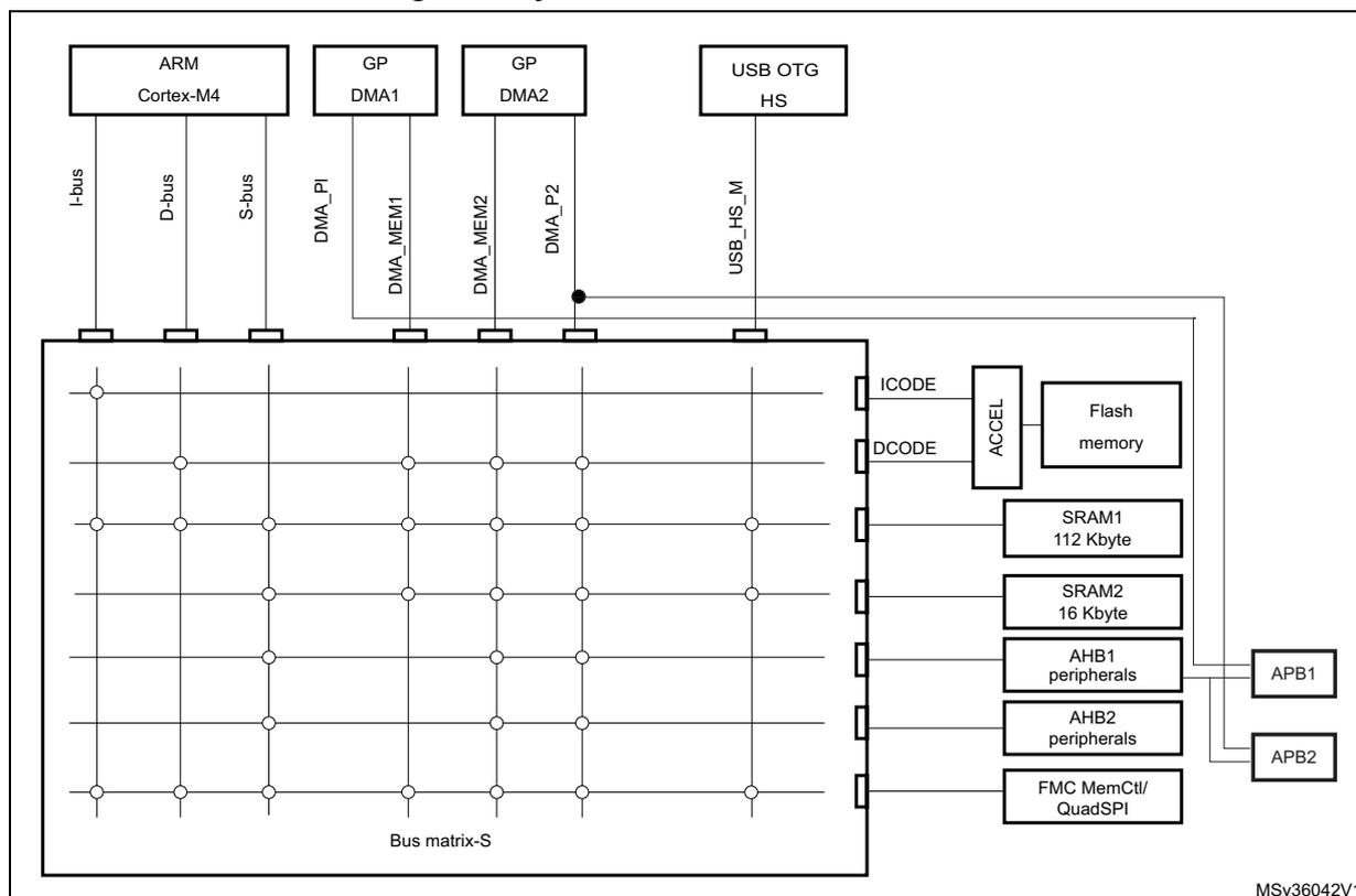
The diagram illustrates the system architecture for STM32F446xx devices. At the top, four master blocks are shown: ARM Cortex-M4, GP DMA1, GP DMA2, and USB OTG HS. The ARM Cortex-M4 is connected to the I-bus, D-bus, and S-bus. GP DMA1 is connected to DMA_PI, DMA_MEM1, and DMA_MEM2. GP DMA2 is connected to DMA_MEM2 and DMA_P2. USB OTG HS is connected to USB_HS_M. All these buses connect to a central 'Bus matrix-S'. From the Bus matrix-S, several slave blocks are connected: Flash memory (via ICODE and DCODE lines), SRAM1 112 Kbyte, SRAM2 16 Kbyte, AHB1 peripherals (connected to APB1), AHB2 peripherals (connected to APB2), and FMC MemCtl/QuadSPI. An ACCEL block is also shown connected to the Flash memory. The diagram is labeled MSv36042V1 at the bottom right.
2.1.1 I-bus
This bus connects the Instruction bus of the Cortex ® -M4 with FPU core to the BusMatrix. This bus is used by the core to fetch instructions. The target of this bus is a memory containing code (internal Flash memory/SRAM or external memories through the FMC).
2.1.2 D-bus
This bus connects the databus of the Cortex ® -M4 with FPU to the BusMatrix. This bus is used by the core for literal load and debug access. The target of this bus is a memory containing code or data (internal Flash memory or external memories through the FMC).
2.1.3 S-bus
This bus connects the system bus of the Cortex ® -M4 with FPU core to a BusMatrix. This bus is used to access data located in a peripheral or in SRAM. Instructions may also be fetch on this bus (less efficient than ICode). The targets of this bus are the internal SRAM, SRAM2, the AHB1 peripherals including the APB peripherals, the AHB2 peripherals and the external memories through the FMC and QUADSPI.
2.1.4 DMA memory bus
This bus connects the DMA memory bus master interface to the BusMatrix. It is used by the DMA to perform transfer to/from memories. The targets of this bus are data memories:
internal Flash, internal SRAMs (SRAM1, SRAM2) and external memories through the FMC and QUADSPI.
2.1.5 DMA peripheral bus
This bus connects the DMA peripheral master bus interface to the BusMatrix. This bus is used by the DMA to access AHB peripherals or to perform memory-to-memory transfers. The targets of this bus are the AHB and APB peripherals plus data memories: internal Flash, internal SRAMs (SRAM1, SRAM2) and external memories through the FMC and the QUADSPI.
2.1.6 USB OTG HS DMA bus
This bus connects the USB OTG HS DMA master interface to the BusMatrix. This bus is used by the USB OTG DMA to load/store data to a memory. The targets of this bus are data memories: internal SRAMs (SRAM1, SRAM2), internal Flash memory, and external memories through the FMC and QUADSPI.
2.1.7 BusMatrix
The BusMatrix manages the access arbitration between masters. The arbitration uses a round-robin algorithm.
2.1.8 AHB/APB bridges (APB)
The two AHB/APB bridges, APB1 and APB2, provide full synchronous connections between the AHB and the two APB buses, allowing flexible selection of the peripheral frequency.
Refer to the device datasheets for more details on APB1 and APB2 maximum frequencies, and to Table 1 for the address mapping of AHB and APB peripherals.
After each device reset, all peripheral clocks are disabled (except for the SRAM and Flash memory interface). Before using a peripheral you have to enable its clock in the RCC_AHBxENR or RCC_APBxENR register.
Note: When a 16- or an 8-bit access is performed on an APB register, the access is transformed into a 32-bit access: the bridge duplicates the 16- or 8-bit data to feed the 32-bit vector.
2.2 Memory organization
2.2.1 Introduction
Program memory, data memory, registers and I/O ports are organized within the same linear 4-Gbyte address space.
The bytes are coded in memory in Little Endian format. The lowest numbered byte in a word is considered the word's least significant byte and the highest numbered byte the most significant.
The addressable memory space is divided into eight main blocks, of 512 Mbytes each.
2.2.2 Memory map and register boundary addresses
Figure 2. Memory map
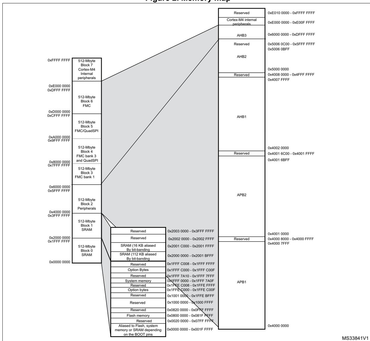
The memory map shows the following main blocks and their sub-structures:
- 0x0000 0000 - 0x2000 0000: SRAM (112 KB aliased By bit-banding) and SRAM (16 KB aliased By bit-banding). Sub-areas include Reserved, Option Bytes, System memory, and Flash memory.
- 0x2000 0000 - 0x4000 0000: SRAM (112 KB aliased By bit-banding) and SRAM (16 KB aliased By bit-banding). Sub-areas include Reserved, Option Bytes, System memory, and Flash memory.
- 0x4000 0000 - 0x6000 0000: 512-Mbyte Block 1 SRAM.
- 0x6000 0000 - 0x8000 0000: 512-Mbyte Block 2 Peripherals.
- 0x8000 0000 - 0xA000 0000: 512-Mbyte Block 3 FMC bank 1.
- 0xA000 0000 - 0xC000 0000: 512-Mbyte Block 4 FMC bank 3 and QuadSPI.
- 0xC000 0000 - 0xE000 0000: 512-Mbyte Block 5 FMC/QuadSPI.
- 0xE000 0000 - 0x1000 0000: 512-Mbyte Block 6 FMC.
- 0x1000 0000 - 0x1200 0000: 512-Mbyte Block 7 Cortex-M4 internal peripherals.
Bus names indicated in the map: AHB1, AHB2, AHB3, APB1.
All the memory map areas that are not allocated to on-chip memories and peripherals are considered “Reserved”. For the detailed mapping of available memory and register areas, refer to the following table.
The following table gives the boundary addresses of the peripherals available in the devices.
Table 1. STM32F446xx register boundary addresses
| Boundary address | Peripheral | Bus | Register map |
|---|---|---|---|
| 0xA000 0000 - 0xA000 0FFF | FMC control register | AHB3 | Section 11.8.6: FMC register map on page 318 |
| 0xA000 1000 - 0xA000 1FFF | QUADSPI register | AHB3 | Section 12.5.14: QUADSPI register map on page 348 |
Table 1. STM32F446xx register boundary addresses (continued)
| Boundary address | Peripheral | Bus | Register map |
|---|---|---|---|
| 0x5005 0000 - 0x5005 03FF | DCMI | AHB2 | Section 15.5.12: DCMI register map on page 438 |
| 0x5000 0000 - 0x5003 FFFF | USB OTG FS | AHB2 | Section 31.15.65: OTG_FS/OTG_HS register map on page 1180 |
| 0x4004 0000 - 0x4007 FFFF | USB OTG HS | AHB1 | Section 31.15.65: OTG_FS/OTG_HS register map on page 1180 |
| 0x4002 6400 - 0x4002 67FF | DMA2 | ||
| 0x4002 6000 - 0x4002 63FF | DMA1 | Section 9.5.11: DMA register map on page 231 | |
| 0x4002 4000 - 0x4002 4FFF | BKPSRAM | ||
| 0x4002 3C00 - 0x4002 3FFF | Flash interface register | - | |
| 0x4002 3800 - 0x4002 3BFF | RCC | Section 3.8: Flash interface registers on page 80 | |
| 0x4002 3000 - 0x4002 33FF | CRC | Section 6.3.28: RCC register map on page 170 | |
| 0x4002 1C00 - 0x4002 1FFF | GPIOH | AHB1 | Section 4.4.4: CRC register map on page 91 |
| 0x4002 1800 - 0x4002 1BFF | GPIOG | Section 7.4.11: GPIO register map on page 191 | |
| 0x4002 1400 - 0x4002 17FF | GPIOF | ||
| 0x4002 1000 - 0x4002 13FF | GPIOE | ||
| 0x4002 0C00 - 0x4002 0FFF | GPIOD | ||
| 0x4002 0800 - 0x4002 0BFF | GPIOC | ||
| 0x4002 0400 - 0x4002 07FF | GPIOB | ||
| 0x4002 0000 - 0x4002 03FF | GPIOA | ||
| 0x4001 5C00 - 0x4001 5FFF | SAI2 | APB2 | Section 28.5.18: SAI register map on page 959 |
| 0x4001 5800 - 0x4001 5BFF | SAI1 | ||
| 0x4001 4800 - 0x4001 4BFF | TIM11 | APB2 | Section 18.5.12: TIM10/11/13/14 register map on page 616 |
| 0x4001 4400 - 0x4001 47FF | TIM10 | ||
| 0x4001 4000 - 0x4001 43FF | TIM9 | ||
| 0x4001 3C00 - 0x4001 3FFF | EXTI | Section 10.3.7: EXTI register map on page 246 | |
| 0x4001 3800 - 0x4001 3BFF | SYSCFG | Section 8.2.9: SYSCFG register map on page 199 | |
| 0x4001 3400 - 0x4001 37FF | SPI4 | APB2 | Section 26.7.10: SPI register map on page 874 |
| 0x4001 3000 - 0x4001 33FF | SPI1 | Section 26.7.10: SPI register map on page 874 | |
| 0x4001 2C00 - 0x4001 2FFF | SDMMC | Section 29.8.16: SDIO register map on page 1016 | |
| 0x4001 2000 - 0x4001 23FF | ADC1 - ADC2 - ADC3 | Section 13.13.18: ADC register map on page 392 | |
| 0x4001 1400 - 0x4001 17FF | USART6 | Section 25.6.8: USART register map on page 824 | |
| 0x4001 1000 - 0x4001 13FF | USART1 | ||
| 0x4001 0400 - 0x4001 07FF | TIM8 | Section 16.4.21: TIM1&TIM8 register map on page 508 | |
| 0x4001 0000 - 0x4001 03FF | TIM1 |
Table 1. STM32F446xx register boundary addresses (continued)
| Boundary address | Peripheral | Bus | Register map |
|---|---|---|---|
| 0x4000 7400 - 0x4000 77FF | DAC | APB1 | Section 14.5.15: DAC register map on page 416 |
| 0x4000 7000 - 0x4000 73FF | PWR | Section 5.5: PWR register map on page 115 | |
| 0x4000 6C00 - 0x4000 6FFF | HDMI-CEC | Section 32.7.7: HDMI-CEC register map on page 1276 | |
| 0x4000 6800 - 0x4000 6BFF | CAN2 | Section 30.9.5: bxCAN register map on page 1058 | |
| 0x4000 6400 - 0x4000 67FF | CAN1 | ||
| 0x4000 5C00 - 0x4000 5FFF | I2C3 | Section 24.6.11: I2C register map on page 773 | |
| 0x4000 5800 - 0x4000 5BFF | I2C2 | ||
| 0x4000 5400 - 0x4000 57FF | I2C1 | ||
| 0x4000 5000 - 0x4000 53FF | UART5 | Section 25.6.8: USART register map on page 824 | |
| 0x4000 4C00 - 0x4000 4FFF | UART4 | ||
| 0x4000 4800 - 0x4000 4BFF | USART3 | ||
| 0x4000 4400 - 0x4000 47FF | USART2 | ||
| 0x4000 4000 - 0x4000 43FF | SPDIF-RX | Section 27.5.10: SPDIFRX interface register map on page 905 | |
| 0x4000 3C00 - 0x4000 3FFF | SPI3 / I2S3 | Section 26.7.10: SPI register map on page 874 | |
| 0x4000 3800 - 0x4000 3BFF | SPI2 / I2S2 | ||
| 0x4000 3000 - 0x4000 33FF | IWDG | Section 20.4.5: IWDG register map on page 635 | |
| 0x4000 2C00 - 0x4000 2FFF | WWDG | Section 21.6.4: WWDG register map on page 642 | |
| 0x4000 2800 - 0x4000 2BFF | RTC & BKP Registers | Section 22.6.21: RTC register map on page 679 | |
| 0x4000 2000 - 0x4000 23FF | TIM14 | Section 18.5.12: TIM10/11/13/14 register map on page 616 | |
| 0x4000 1C00 - 0x4000 1FFF | TIM13 | ||
| 0x4000 1800 - 0x4000 1BFF | TIM12 | ||
| 0x4000 1400 - 0x4000 17FF | TIM7 | Section 19.4.9: TIM6&TIM7 register map on page 629 | |
| 0x4000 1000 - 0x4000 13FF | TIM6 | ||
| 0x4000 0C00 - 0x4000 0FFF | TIM5 | Section 17.4.21: TIMx register map on page 569 | |
| 0x4000 0800 - 0x4000 0BFF | TIM4 | ||
| 0x4000 0400 - 0x4000 07FF | TIM3 | ||
| 0x4000 0000 - 0x4000 03FF | TIM2 |
2.2.3 Embedded SRAM
The STM32F446xx feature 4 Kbytes of backup SRAM (see Section 5.1.2: Battery backup domain (also known as RTC domain) ) plus 128 Kbytes of system SRAM.
The embedded SRAM can be accessed as bytes, half-words (16 bits) or full words (32 bits). Read and write operations are performed at CPU speed with 0 wait state. The embedded SRAM is divided into up to two blocks:
- • SRAM1 and SRAM2 mapped at address 0x2000 0000 and accessible by all AHB masters.
The AHB masters support concurrent SRAM accesses (from the USB OTG HS): for instance, the USB OTG HS can read/write from/to SRAM2 while the CPU is reading/writing from/to SRAM1.
The CPU can access the SRAM1 and SRAM2 through the System bus or through the I-Code/D-Code buses when boot from SRAM is selected or when physical remap is selected ( Section 8.2.1: SYSCFG memory remap register (SYSCFG_MEMRMP) in the SYSCFG controller). To get the maximum performance on SRAM execution, physical remap should be selected (boot or software selection).
2.2.4 Flash memory overview
The Flash memory interface manages CPU AHB I-Code and D-Code accesses to the Flash memory. It implements the erase and program Flash memory operations and the read and write protection mechanisms. It accelerates code execution with a system of instruction prefetch and cache lines.
The Flash memory is organized as follows:
- • A main memory block divided into sectors.
- • System memory from which the device boots in System memory boot mode
- • 512 OTP (one-time programmable) bytes for user data.
- • Option bytes to configure read and write protection, BOR level, watchdog software/hardware and reset when the device is in Standby or Stop mode.
Refer to Section 3: Embedded flash memory interface for more details.
2.2.5 Bit banding
The Cortex ® -M4 with FPU memory map includes two bit-band regions. These regions map each word in an alias region of memory to a bit in a bit-band region of memory. Writing to a word in the alias region has the same effect as a read-modify-write operation on the targeted bit in the bit-band region.
In the STM32F446xx devices both the peripheral registers and the SRAM are mapped to a bit-band region, so that single bit-band write and read operations are allowed. The operations are only available for Cortex ® -M4 with FPU accesses, and not from other bus masters (e.g. DMA).
A mapping formula shows how to reference each word in the alias region to a corresponding bit in the bit-band region. The mapping formula is:
where:
- – bit_word_addr is the address of the word in the alias memory region that maps to the targeted bit
- – bit_band_base is the starting address of the alias region
- – byte_offset is the number of the byte in the bit-band region that contains the targeted bit
- – bit_number is the bit position (0-7) of the targeted bit
Example
The following example shows how to map bit 2 of the byte located at SRAM address 0x20000300 to the alias region:
Writing to address 0x22006008 has the same effect as a read-modify-write operation on bit 2 of the byte at SRAM address 0x20000300.
Reading address 0x22006008 returns the value (0x01 or 0x00) of bit 2 of the byte at SRAM address 0x20000300 (0x01: bit set; 0x00: bit reset).
For more information on bit-banding, refer to the Cortex®-M4 with FPU programming manual (see Related documents on page 1 ).
2.3 Boot configuration
Due to its fixed memory map, the code area starts from address 0x0000 0000 (accessed through the ICode/DCode buses) while the data area (SRAM) starts from address 0x2000 0000 (accessed through the system bus). The Cortex®-M4 with FPU CPU always fetches the reset vector on the ICode bus, which implies to have the boot area available only in the code area (typically, Flash memory). STM32F446xx microcontrollers implement a special mechanism to be able to boot from other memories (like the internal SRAM).
In the STM32F446xx, three different boot modes can be selected through the BOOT[1:0] pins as shown in Table 2 .
Table 2. Boot modes
| Boot mode selection pins | Boot mode | Aliasing | |
|---|---|---|---|
| BOOT1 | BOOT0 | ||
| x | 0 | Main Flash memory | Main Flash memory is selected as the boot area |
| 0 | 1 | System memory | System memory is selected as the boot area |
| 1 | 1 | Embedded SRAM | Embedded SRAM is selected as the boot area |
The values on the BOOT pins are latched on the 4th rising edge of SYSCLK after a reset. It is up to the user to set the BOOT1 and BOOT0 pins after reset to select the required boot mode.
BOOT0 is a dedicated pin while BOOT1 is shared with a GPIO pin. Once BOOT1 has been sampled, the corresponding GPIO pin is free and can be used for other purposes.
The BOOT pins are also resampled when the device exits the Standby mode. Consequently, they must be kept in the required Boot mode configuration when the device is in the Standby mode. After this startup delay is over, the CPU fetches the top-of-stack value from address 0x0000 0000, then starts code execution from the boot memory starting from 0x0000 0004.
Note: When the device boots from SRAM, in the application initialization code, you have to relocate the vector table in SRAM using the NVIC exception table and the offset register.
Embedded bootloader
The embedded bootloader mode is used to reprogram the Flash memory using one of the following serial interfaces:
- • USART
- • CAN2
- • I2C
- • SPI
- • USB OTG FS in Device mode (DFU: device firmware upgrade).
The USART peripherals operate at the internal 16 MHz oscillator (HSI) frequency, while the CAN and USB OTG FS require an external clock (HSE) multiple of 1 MHz (ranging from 4 to 26 MHz).
The embedded bootloader code is located in system memory. It is programmed by ST during production. For additional information, refer to application note AN2606.
Physical remap in STM32F446xx
Once the boot pins are selected, the application software can modify the memory accessible in the code area (in this way the code can be executed through the ICode bus in place of the System bus). This modification is performed by programming the Section 8.2.1: SYSCFG memory remap register (SYSCFG_MEMRMP) in the SYSCFG controller.
The following memories can thus be remapped:
- • Main Flash memory
- • System memory
- • Embedded SRAM1 (112 KB)
- • FMC bank 1 (NOR/PSRAM 1 and 2)
- • FMC SDRAM bank 1
Table 3. Memory mapping vs. Boot mode/physical remap in STM32F446xx
| Addresses | Boot/Remap in main Flash memory | Boot/Remap in embedded SRAM | Boot/Remap in System memory | Remap in FMC |
|---|---|---|---|---|
| 0x2001 C000 - 0x2001 FFFF | SRAM2 (16 KB) | SRAM2 (16 KB) | SRAM2 (16 KB) | SRAM2 (16 KB) |
| 0x2000 0000 - 0x2001 BFFF | SRAM1 (112 KB) | SRAM1 (112 KB) | SRAM1 (112 KB) | SRAM1 (112 KB) |
| 0x1FFF 0000 - 0x1FFF 77FF | System memory | System memory | System memory | System memory |
| 0x0810 0000 - 0x0FFF FFFF | Reserved | Reserved | Reserved | Reserved |
| 0x0800 0000 - 0x081F FFFF | Flash memory | Flash memory | Flash memory | Flash memory |
| Addresses | Boot/Remap in main Flash memory | Boot/Remap in embedded SRAM | Boot/Remap in System memory | Remap in FMC |
|---|---|---|---|---|
| 0x0400 0000 - 0x07FF FFFF | Reserved | Reserved | Reserved | FMC bank 1 NOR/PSRAM 2 (128 MB Aliased) |
| 0x0000 0000 - 0x001F FFFF (1)(2) | Flash (512 KB) Aliased | SRAM1 (112 KB) Aliased | System memory (30 KB) Aliased | FMC bank 1 NOR/PSRAM 1 (128 MB Aliased) or FMC SDRAM bank 1 (128 MB Aliased) |
- 1. When the FMC is remapped at address 0x0000 0000, only the first two regions of bank 1 memory controller (bank 1 NOR/PSRAM 1 and NOR/PSRAM 2) or SDRAM bank 1 can be remapped. In remap mode, the CPU can access the external memory via ICode bus instead of System bus which boosts up the performance.
- 2. Even when aliased in the boot memory space, the related memory is still accessible at its original memory space.