20. Cryptographic processor (CRYP)
This section applies to all STM32F479xx devices, unless otherwise specified.
20.1 Introduction
The cryptographic processor (CRYP) can be used both to encrypt and decrypt data using the DES, Triple-DES or AES algorithms. It is a fully compliant implementation of the following standards:
- • The data encryption standard (DES) and Triple-DES (TDES) as defined by Federal Information Processing Standards Publication (FIPS PUB 46-3, Oct 1999), and the American National Standards Institute (ANSI X9.52)
- • The advanced encryption standard (AES) as defined by Federal Information Processing Standards Publication (FIPS PUB 197, Nov 2001)
Multiple key sizes and chaining modes are supported:
- • DES/TDES chaining modes ECB and CBC, supporting standard 56-bit keys with 8-bit parity per key
- • AES chaining modes ECB, CBC, CTR, GCM, GMAC, CCM for key sizes of 128, 192 or 256 bits
The CRYP processor is a 32-bit AHB peripheral. It supports DMA transfers for incoming and outgoing data (two DMA channels are required). The peripheral also includes input and output FIFOs (each 8 words deep) for better performance.
20.2 CRYP main features
- • Compliant implementation of the following standards:
- – NIST FIPS publication 46-3, Data Encryption Standard (DES)
- – ANSI X9.52, Triple Data Encryption Algorithm Modes of Operation
- – NIST FIPS publication 197, Advanced Encryption Standard (AES)
- • AES symmetric block cipher implementation
- – 128-bit data block processing
- – Support for 128-, 192- and 256-bit cipher key lengths
- – Encryption and decryption with multiple chaining modes: Electronic Code Book (ECB), Cipher Block Chaining (CBC), Counter mode (CTR), Galois Counter Mode (GCM), Galois Message Authentication Code mode (GMAC) and Counter with CBC-MAC (CCM)
- – 14 (respectively 18) clock cycles for processing one 128-bit block of data with a 128-bit (respectively 256-bit) key in AES-ECB mode
- – Integrated key scheduler with its key derivation stage (ECB or CBC decryption only)
- • DES/TDES encryption/decryption implementation
- – 64-bit data block processing
- – Support for 64-, 128- and 192-bit cipher key lengths (including parity)
- – Encryption and decryption with support of ECB and CBC chaining modes
- – Direct implementation of simple DES algorithms (a single key K1 is used)
- – 16 (respectively 48) clock cycles for processing one 64-bit block of data in DES (respectively TDES) ECB mode
- – Software implementation of ciphertext stealing
- • Features common to DES/TDES and AES
- – AMBA AHB target peripheral, accessible through 32-bit word single accesses only (otherwise an AHB bus error is generated, and write accesses are ignored)
- – 256-bit register for storing the cryptographic key (8x 32-bit registers)
- – 128-bit registers for storing initialization vectors (4x 32-bit)
- – 1x32-bit INPUT buffer associated with an internal IN FIFO of eight 32- bit words, corresponding to four incoming DES blocks or two AES blocks
- – 1x32-bit OUTPUT buffer associated with an internal OUT FIFO of eight 32-bit words, corresponding to four processed DES blocks or two AES blocks
- – Automatic data flow control supporting direct memory access (DMA) using two channels (one for incoming data, one for processed data). The OUT FIFO supports both single and burst transfers, while the IN FIFO supports only burst transfers.
- – Data swapping logic to support 1-, 8-, 16- or 32-bit data
- – Possibility for software to suspend a message if the cryptographic processor needs to process another message with higher priority (suspend/resume operation)
20.3 CRYP implementation
This device has one CRYP instance.
20.4 CRYP functional description
20.4.1 CRYP block diagram
The figure below shows the block diagram of the cryptographic processor.
Figure 158. CRYP block diagram
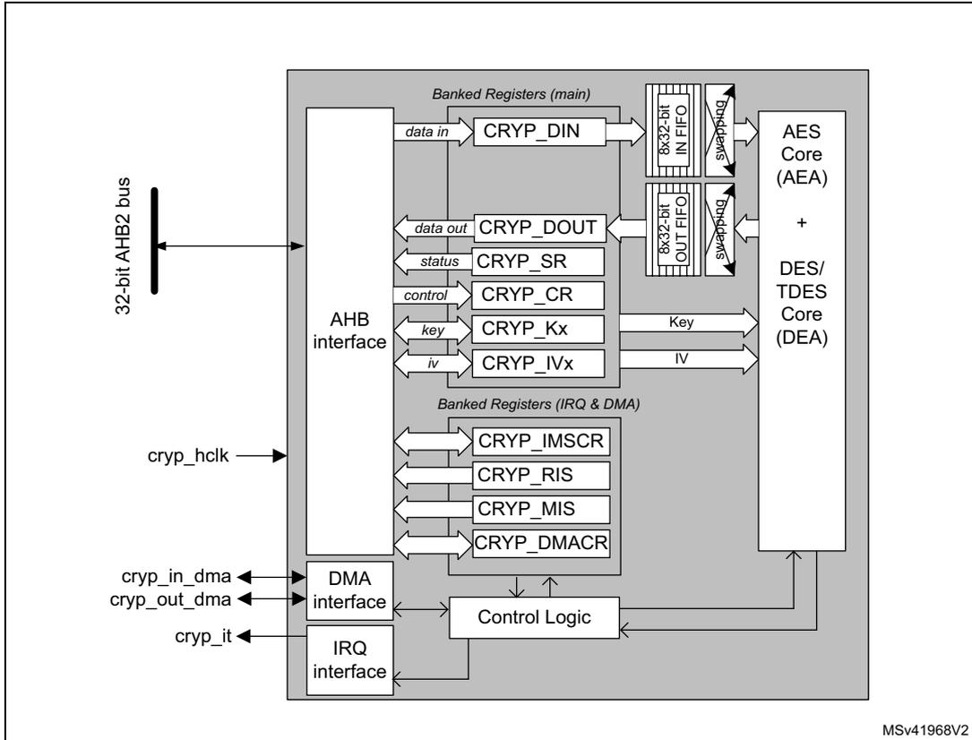
The diagram illustrates the internal architecture of the CRYP block. On the left, a 32-bit AHB2 bus connects to an AHB interface. The AHB interface is connected to two sets of registers: 'Banked Registers (main)' containing CRYP_DIN, CRYP_DOUT, CRYP_SR, CRYP_CR, CRYP_Kx, and CRYP_IVx; and 'Banked Registers (IRQ & DMA)' containing CRYP_IMSCR, CRYP_RIS, CRYP_MIS, and CRYP_DMACR. CRYP_DIN feeds into an 'IN FIFO' (8x32-bit), which connects to the 'AES Core (AEA)'. CRYP_DOUT is fed from an 'OUT FIFO' (8x32-bit) from the 'DES/TDES Core (DEA)'. CRYP_Kx and CRYP_IVx provide 'Key' and 'IV' inputs to both the AEA and DEA cores. A 'Control Logic' block is connected to the DMA interface, IRQ interface, and the registers. The DMA interface handles 'cryp_in_dma' and 'cryp_out_dma' signals. The IRQ interface generates the 'cryp_it' signal. The 'cryp_hclk' signal is provided to the AHB interface and Control Logic. A small note 'MSV41968V2' is present in the bottom right corner.
20.4.2 CRYP internal signals
Table 141 provides a list of useful-to-know internal signals available at cryptographic processor level and not at STM32 product level (on pads).
Table 141. CRYP internal input/output signals
| Signal name | Signal type | Description |
|---|---|---|
| cryp_hclk | Digital input | AHB bus clock |
| cryp_it | Digital output | Cryptographic processor global interrupt request |
| cryp_in_dma | Digital input/output | IN FIFO DMA burst request/ acknowledge |
| cryp_out_dma | Digital input/output | OUT FIFO DMA burst request/ acknowledge (with single request for DES/TDES) |
20.4.3 CRYP DES/TDES cryptographic core
Overview
The DES/Triple-DES cryptographic core consists of three components:
- • The DES Algorithm (DEA core)
- • Multiple keys (one for the DES algorithm, one to three for the TDES algorithm)
- • The initialization vector, which is used only in CBC mode
The DES/Triple-DES cryptographic core provides two operating modes:
- • ALGODIR = 0: Plaintext encryption using the key stored in the CRYP_Kx registers.
- • ALGODIR = 1: Ciphertext decryption using the key stored in the CRYP_Kx registers.
The operating mode is selected by programming the ALGODIR bit in the CRYP_CR register.
Typical data processing
Typical usage of the cryptographic processor in DES modes can be found in Section 20.4.10: CRYP DES/TDES basic chaining modes (ECB, CBC) .
Note: The outputs of the intermediate DEA stages are never revealed outside the cryptographic boundary, with the exclusion of the IV registers in CBC mode.
DES/TDES keying and chaining modes
The DES/TDES allows three different keying options:
- • Three independent keys
The first option specifies that all the keys are independent, that is, K1, K2 and K3 are independent. FIPS PUB 46-3 – 1999 (and ANSI X9.52 – 1998) refers to this option as the Keying Option 1 and, to the TDES as 3-key TDES.
- • Two independent keys
The second option specifies that K1 and K2 are independent and K3 is equal to K1, that is, K1 and K2 are independent, K3 = K1. FIPS PUB 46-3 – 1999 (and ANSI X9.52 – 1998) refers to this second option as the Keying Option 2 and, to the TDES as 2-key TDES.
- • Three equal keys
The third option specifies that K1, K2 and K3 are equal, that is:
FIPS PUB 46-3 – 1999 (and ANSI X9.52 – 1998) refers to the third option as the Keying Option 3. This “1-key” TDES is equivalent to single DES.
The following chaining algorithms are supported by the DES hardware and can be selected through the ALGOMODE bits in the CRYP_CR register:
- • Electronic Code Book (ECB)
- • Cipher Block Chaining (CBC)
These modes are described in details in Section 20.4.10: CRYP DES/TDES basic chaining modes (ECB, CBC) .
20.4.4 CRYP AES cryptographic core
Overview
The AES cryptographic core consists of the following components:
- • The AES algorithm (AEA core)
- • The Multiplier over a binary Galois field (GF2mul)
- • The key information
- • The initialization vector (IV) or Nonce information
- • Chaining algorithms logic (XOR, feedback/counter, mask)
The AES core works on 128-bit data blocks of (four words) with 128-, 192- or 256-bit key lengths. Depending on the chaining mode, the peripheral requires zero or one 128-bit initialization vector (IV).
The cryptographic peripheral features two operating modes:
- • ALGODIR = 0: Plaintext encryption using the key stored in the CRYP_Kx registers.
- • ALGODIR = 1: Ciphertext decryption using the key stored in the CRYP_Kx registers. When ECB and CBC chaining modes are selected, an initial key derivation process is automatically performed by the cryptographic peripheral.
The operating mode is selected by programming the ALGODIR bit in the CRYP_CR register.
Typical data processing
A description of cryptographic processor typical usage in AES mode can be found in Section 20.4.11: CRYP AES basic chaining modes (ECB, CBC) .
Note: The outputs of the intermediate AEA stages is never revealed outside the cryptographic boundary, with the exclusion of the IV registers.
AES chaining modes
The following chaining algorithms are supported by the cryptographic processor and can be selected through the ALGOMODE bits in the CRYP_CR register:
- • Electronic Code Book (ECB)
- • Cipher Block Chaining (CBC)
- • Counter Mode (CTR)
- • Galois/Counter Mode (GCM)
- • Galois Message Authentication Code mode (GMAC)
- • Counter with CBC-MAC (CCM)
A quick introduction on these chaining modes can be found in the following subsections.
For detailed instructions, refer to Section 20.4.11: CRYP AES basic chaining modes (ECB, CBC) and onward.
AES Electronic CodeBook (ECB) Figure 159. AES-ECB mode overview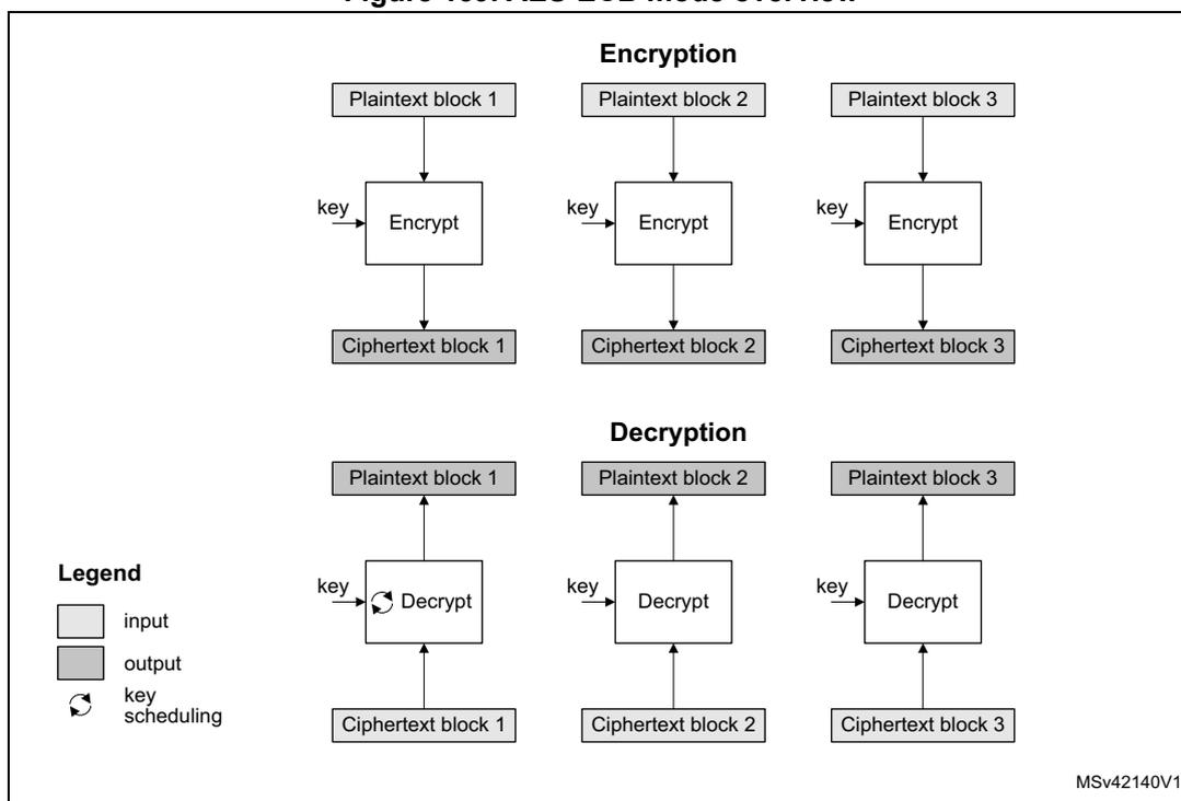
The diagram illustrates the AES-ECB mode of operation, divided into two sections: Encryption and Decryption .
Encryption: Three separate plaintext blocks (Plaintext block 1, 2, and 3) are each processed by an Encrypt block. Each Encrypt block takes a key as input and produces a corresponding ciphertext block (Ciphertext block 1, 2, and 3).
Decryption: Three separate ciphertext blocks (Ciphertext block 1, 2, and 3) are each processed by a Decrypt block. Each Decrypt block takes a key as input and produces a corresponding plaintext block (Plaintext block 1, 2, and 3). A circular arrow icon next to the key input of the first Decrypt block indicates a special key scheduling requirement.
Legend:
- input (white box)
- output (gray box)
- key scheduling (circular arrow icon)
MSv42140V1
ECB is the simplest operating mode. There are no chaining operations, and no special initialization stage. The message is divided into blocks and each block is encrypted or decrypted separately.
Note: For decryption, a special key scheduling is required before processing the first block.
AES Cipher block chaining (CBC)
Figure 160. AES-CBC mode overview
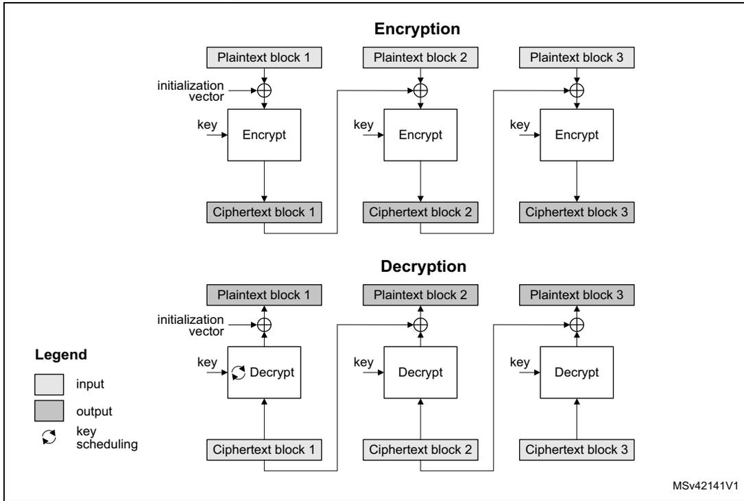
The diagram illustrates the AES-CBC mode of operation for encryption and decryption across three blocks.
Encryption:
- Plaintext block 1 is XORed with the initialization vector and then passed through an Encrypt block using a key to produce Ciphertext block 1 .
- Plaintext block 2 is XORed with the output of the previous block ( Ciphertext block 1 ) and then passed through an Encrypt block using the same key to produce Ciphertext block 2 .
- Plaintext block 3 is XORed with the output of the previous block ( Ciphertext block 2 ) and then passed through an Encrypt block using the same key to produce Ciphertext block 3 .
Decryption:
- Ciphertext block 1 is passed through a Decrypt block using a key to produce Plaintext block 1 . The initialization vector is XORed with the output of the decrypt block.
- Ciphertext block 2 is passed through a Decrypt block using the same key to produce Plaintext block 2 . The output of the previous block ( Ciphertext block 1 ) is XORed with the output of the decrypt block.
- Ciphertext block 3 is passed through a Decrypt block using the same key to produce Plaintext block 3 . The output of the previous block ( Ciphertext block 2 ) is XORed with the output of the decrypt block.
Legend:
- input (white box)
- output (grey box)
- key scheduling (circular arrow)
MSv42141V1
CBC operating mode chains the output of each block with the input of the following block. To make each message unique, an initialization vector is used during the first block processing.
Note: For decryption, a special key scheduling is required before processing the first block.
AES Counter mode (CTR)
Figure 161. AES-CTR mode overview
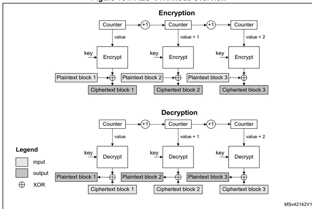
The diagram illustrates the AES Counter mode (CTR) for encryption and decryption. It is divided into two main sections: Encryption and Decryption .
Encryption: A sequence of three Counter blocks is shown. The first Counter outputs its value to an Encrypt block. The second Counter outputs value + 1 to an Encrypt block. The third Counter outputs value + 2 to an Encrypt block. Each Encrypt block also receives a key . The output of each Encrypt block is XORed (indicated by \( \oplus \) ) with a corresponding Plaintext block (1, 2, or 3) to produce a Ciphertext block (1, 2, or 3). The Counter blocks are chained: the first is initialized, and subsequent ones are incremented by +1 from the previous one.
Decryption: The process is identical to encryption, but the Encrypt blocks are replaced by Decrypt blocks. The Decrypt blocks take the same counter values and key as the Encrypt blocks. The output of each Decrypt block is XORed with the corresponding Ciphertext block (1, 2, or 3) to recover the Plaintext block (1, 2, or 3).
Legend:
- input (light gray box)
- output (dark gray box)
- \( \oplus \) XOR
MSv42142V1
The CTR mode uses the AES core to generate a key stream; these keys are then XORed with the plaintext to obtain the ciphertext as specified in NIST Special Publication 800-38A, Recommendation for Block Cipher Modes of Operation .
Note: Unlike ECB and CBC modes, no key scheduling is required for the CTR decryption, since in this chaining scheme the AES core is always used in encryption mode for producing the counter blocks.
AES Galois/Counter mode (GCM)
Figure 162. AES-GCM mode overview
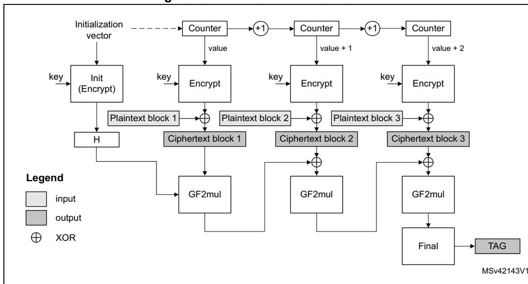
The diagram illustrates the AES-GCM mode of operation. It starts with an Initialization vector and a key being input to an Init (Encrypt) block. This block produces an H value. The Initialization vector is also passed to a Counter block. The Counter block outputs a value , which is input to an Encrypt block along with the key . The Encrypt block outputs Plaintext block 1 , which is XORed with the value to produce Ciphertext block 1 . The Counter block also outputs value + 1 , which is input to the next Encrypt block. This process repeats for Plaintext block 2 and Plaintext block 3 , resulting in Ciphertext block 2 and Ciphertext block 3 . The H value and the ciphertext blocks are input to GF2mul blocks. The outputs of the GF2mul blocks are XORed together and then input to a Final block, which produces the TAG . A legend indicates that white boxes are input , grey boxes are output , and the circle with a cross symbol represents XOR . The diagram is labeled MSv42143V1.
In Galois/Counter mode (GCM), the plaintext message is encrypted, while a message authentication code (MAC) is computed in parallel, thus generating the corresponding ciphertext and its MAC (also known as authentication tag). It is defined in NIST Special Publication 800-38D, Recommendation for Block Cipher Modes of Operation - Galois/Counter Mode (GCM) and GMAC .
GCM mode is based on AES in counter mode for confidentiality. It uses a multiplier over a fixed finite field for computing the message authentication code. It requires an initial value and a particular 128-bit block at the end of the message.
AES Galois message authentication code (GMAC)
Figure 163. AES-GMAC mode overview
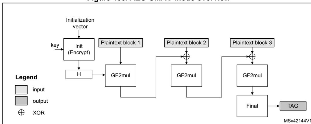
The diagram illustrates the AES-GMAC mode of operation. It starts with an Initialization vector and a key being input to an Init (Encrypt) block. This block produces an H value. The Initialization vector is also passed to a GF2mul block along with the H value. The GF2mul block outputs a value that is XORed with Plaintext block 1 to produce Plaintext block 2 . This process repeats for Plaintext block 3 . The final output is input to a Final block, which produces the TAG . A legend indicates that white boxes are input , grey boxes are output , and the circle with a cross symbol represents XOR . The diagram is labeled MSv42144V1.
Galois Message Authentication Code (GMAC) allows authenticating a message and generating the corresponding message authentication code (MAC). It is defined in NIST Special Publication 800-38D, Recommendation for Block Cipher Modes of Operation - Galois/Counter Mode (GCM) and GMAC .
GMAC is similar to Galois/Counter mode (GCM), except that it is applied on a message composed only by clear-text authenticated data (i.e. only header, no payload).
AES Counter with CBC-MAC (CCM)
Figure 164. AES-CCM mode overview
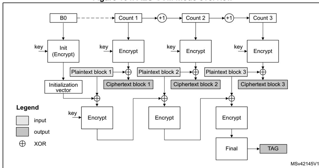
The diagram illustrates the AES-CCM mode of operation. It consists of two main parts: the CTR mode for encryption and the CBC-MAC mode for authentication.
- CTR Mode (Encryption):
- Starts with \( B_0 \) (Initialization vector).
- \( B_0 \) is input to an Init (Encrypt) block along with a key .
- The output of Init (Encrypt) is XORed with Plaintext block 1 to produce Ciphertext block 1 .
- \( B_0 \) is also incremented by 1 to produce Count 1 .
- Count 1 is input to an Encrypt block along with the key .
- The output of Encrypt is XORed with Plaintext block 2 to produce Ciphertext block 2 .
- Count 1 is incremented by 1 to produce Count 2 .
- Count 2 is input to an Encrypt block along with the key .
- The output of Encrypt is XORed with Plaintext block 3 to produce Ciphertext block 3 .
- Count 2 is incremented by 1 to produce Count 3 .
- CBC-MAC Mode (Authentication):
- The Initialization vector (output of Init (Encrypt) ) is input to an Encrypt block along with the key .
- The output of this Encrypt block is XORed with Ciphertext block 1 and then input to another Encrypt block along with the key .
- The output of this Encrypt block is XORed with Ciphertext block 2 and then input to a third Encrypt block along with the key .
- The output of this third Encrypt block is input to a Final block, which produces the TAG (Message Authentication Code).
Legend:
- input (light gray box)
- output (dark gray box)
- XOR ( \( \oplus \) symbol)
MSv42145V1
In Counter with Cipher Block Chaining-Message Authentication Code (CCM), the plaintext message is encrypted while a message authentication code (MAC) is computed in parallel, thus generating the corresponding ciphertext and the corresponding MAC (also known as tag). It is described by NIST in Special Publication 800-38C, Recommendation for Block Cipher Modes of Operation - The CCM Mode for Authentication and Confidentiality .
CCM mode is based on AES in counter mode for confidentiality and it uses CBC for computing the message authentication code. It requires an initial value.
Like GCM CCM chaining mode, AES-CCM mode can be applied on a message composed only by cleartext authenticated data (i.e. only header, no payload). Note that this way of using CCM is not called CMAC (it is not similar to GCM/GMAC), and its usage is not recommended by NIST.
20.4.5 CRYP procedure to perform a cipher operation
Introduction
To understand how the cryptographic peripheral operates, a typical cipher operation is described below. For the detailed peripheral usage according to the cipher mode, refer to the specific section, for example Section 20.4.11: CRYP AES basic chaining modes (ECB, CBC) .
CRYP initialization
To initialize the cryptographic processor, first disable it by clearing the CRYPTEN bit in the CRYP_CR register. Then execute the following steps:
- 1. Configure the algorithm and the chaining mode through the ALGOMODE and ALGODIR bits in the CRYP_CR register. Configure also the key size with the KEYSIZE bits.
- – When ALGODIR is set to 1 (decryption) and the selected algorithm/chaining mode is AES-ECB or AES-CBC, an initial key derivation of the encryption key must be performed as described in Section 20.4.7: Preparing the CRYP AES key for decryption .
- 2. When the previous step is complete, and when applicable, write the symmetric key into the CRYP_KxL/R registers. The way to write key registers is defined in Section 20.4.17: CRYP key registers
- 3. Configure the data type (1, 8, 16 or 32 bits) through the DATATYPE bits of the CRYP_CR register.
- 4. When it is required (for example for CBC or CTR chaining modes), write the initialization vectors into the CRYP_IVx(L/R)R register.
- 5. Flush the IN and OUT FIFOs by writing the FFLUSH bit to 1 in the CRYP_CR register.
Preliminary warning for all cases
If the ECB or CBC mode is selected and data are not a multiple of 64 bits (for DES) or 128 bits (for AES), the second and the last block management is more complex than the sequences below. Refer to Section 20.4.8: CRYP stealing and data padding for more details.
Appending data using the CPU in Polling mode
- 1. Enable the cryptographic processor by setting to 1 the CRYPTEN bit in the CRYP_CR register.
- 2. Write data in the IN FIFO (one block or until the FIFO is full).
- 3. Repeat the following sequence until the second last block of data has been processed:
- a) Wait until the not-empty-flag OFNE is set to 1, then read the OUT FIFO (one block or until the FIFO is empty).
- b) Wait until the not-full-flag IFNF is set to 1, then write the IN FIFO (one block or until the FIFO is full) except if it is the last block.
- 4. The BUSY bit is set automatically by the cryptographic processor. At the end of the processing, the BUSY bit returns to 0 and both FIFOs are empty (IN FIFO empty flag IFEM = 1 and OUT FIFO not empty flag OFNE = 0).
- 5. If the next processing block is the last block, the CPU must pad (when applicable) the data with zeroes to obtain a complete block
- 6. When the operation is complete, the cryptographic processor can be disabled by clearing the CRYPTEN bit in CRYP_CR register.
Appending data using the CPU in Interrupt mode
- 1. Enable the interrupts by setting the INIM and OUTIM bits in the CRYP_IMSCR register.
- 2. Enable the cryptographic processor by setting to 1 the CRYPTEN bit in the CRYP_CR register.
- 3. In the interrupt service routine that manages the input data:
- a) If the last block is being loaded, the CPU must pad (when applicable) the data with zeroes to have a complete block. Then load the block into the IN FIFO.
- b) If it is not the last block, load the data into the IN FIFO. You can load only one block (2 words for DES, 4 words for AES), or load data until the FIFO is full.
- c) In all cases, after the last word of data has been written, disable the interrupt by clearing the INIM interrupt mask.
- 4. In the interrupt service routine that manages the input data:
- a) Read the output data from the OUT FIFO. You can read only one block (2 words for DES, 4 words for AES), or read data until the FIFO is empty.
- b) When the last word has been read, INIM and BUSY bits are set to 0 and both FIFOs are empty (IFEM = 1 and OFNE = 0). You can disable the interrupt by clearing the OUTIM bit, and disable the peripheral by clearing the CRYPTEN bit.
- c) If you read the last block of cleartext data (i.e. decryption), optionally discard the data that is not part of message/payload.
Appending data using the DMA
- 1. Prepare the last block of data by optionally padding it with zeroes to have a complete block.
- 2. Configure the DMA controller to transfer the input data from the memory and transfer the output data from the peripheral to the memory, as described in Section 20.4.19 .
CRYP DMA interface. The DMA should be configured to set an interrupt on transfer completion to indicate that the processing is complete.
- 3. Enable the cryptographic processor by setting to 1 the CRYPTEN bit in CRYP_CR register, then enable the DMA IN and OUT requests by setting to 1 the DIEN and DOEN bits in the CRYP_DMACR register.
- 4. All the transfers and processing are managed by the DMA and the cryptographic processor. The DMA interrupt indicates that the processing is complete. Both FIFOs are normally empty and BUSY flag is set 0.
Caution: It is important that DMA controller empties the cryptographic processor output FIFO before filling up the cryptographic processor input FIFO. To achieve this, the DMA controller should be configured so that the transfer from the cryptographic peripheral to the memory has a higher priority than the transfer from the memory to the cryptographic peripheral.
20.4.6 CRYP busy state
The cryptographic processor is busy and processing data (BUSY set to 1 in CRYP_SR register) when all the conditions below are met:
- • CRYPTEN = 1 in CRYP_CR register.
- • There are enough data in the input FIFO (at least two words for the DES or TDES algorithm mode, four words for the AES algorithm mode).
- • There is enough free-space in the output FIFO (at least two word locations for DES, four for AES).
Write operations to the CRYP_Kx(L/R)R key registers, to the CRYP_IVx(L/R)R initialization registers, or to bits [9:2] of the CRYP_CR register, are ignored when cryptographic processor is busy (i.e. the registers are not modified). It is thus not possible to modify the configuration of the cryptographic processor while it is processing a data block.
It is possible to clear the CRYPTEN bit while BUSY bit is set to 1. In this case the ongoing DES/TDES or AES processing first completes (i.e. the word results are written to the output FIFO) before the BUSY bit is cleared by hardware.
Note: If the application needs to suspend a message to process another one with a higher priority, refer to Section 20.4.9: CRYP suspend/resume operations
When a block is being processed in DES or TDES mode, if the output FIFO becomes full and the input FIFO contains at least one new block, then the new block is popped off the input FIFO and the BUSY bit remains high until there is enough space to store this new block into the output FIFO.
20.4.7 Preparing the CRYP AES key for decryption
When performing an AES ECB or CBC decryption , the AES key has to be prepared. Indeed, in AES encryption the round 0 key is the one stored in the key registers, and AES decryption must start using the last round key. Hence, as the encryption key is stored in memory, a special key scheduling must be performed to obtain the decryption key. This preparation is not required in any other AES modes than ECB or CBC decryption.
When the cryptographic processor is disabled (CRYPEN = 0), the CRYP key preparation process is performed as follows:
- 1. Program ALGOMODE bits to 0x7 and ALGODIR to 0x0 in CRYP_CR. In addition, configure the key length with the KEYSIZE bits.
- 2. Write the symmetric key to the CRYP_KxL/R registers, as described in Section 20.4.17: CRYP key registers .
- 3. Enable the cryptographic processor by setting the CRYPEN bit in the CRYP_CR register. It immediately starts an AES round for key preparation (BUSY = 1).
- 4. Wait until the BUSY bit is cleared in the CRYP_SR register. Then update ALGOMODE bits in the CRYP_CR register to select the correct chaining mode, that is 0x4 for ECB or 0x5 for CBC.
- 5. The AES key is available in the CRYP key registers, ready to use for decryption.
Note: As the CRYPEN bitfield is reset by hardware at the end of the key preparation, the application software must set it again for the next operation.
The latency of the key preparation operation is 14, 16 or 18 clock cycles depending on the key size (128, 192 or 256 bits).
20.4.8 CRYP stealing and data padding
When using DES or AES algorithm in ECB or CBC modes to manage messages that are not multiple of the block size (64 bits for DES, 128 bits for AES), use ciphertext stealing techniques such as those described in NIST Special Publication 800-38A, Recommendation for Block Cipher Modes of Operation: Three Variants of Ciphertext Stealing for CBC Mode . Since the cryptographic processor does not implement such techniques, the last two blocks must be handled in a special way by the application.
Note: Ciphertext stealing techniques are not documented in this reference manual.
Similarly, when the AES algorithm is used in other modes than ECB or CBC, incomplete input data blocks (i.e. block shorter than 128 bits) have to be padded with zeroes by the application prior to encryption (i.e. extra bits should be appended to the trailing end of the data string). After decryption, the extra bits have to be discarded. The cryptographic processor does not implement automatic data padding operation to the last block , so the application should follow the recommendation given in Section 20.4.5: CRYP procedure to perform a cipher operation to manage messages that are not multiple of 128 bits.
Note: Padding data are swapped in a similar way as normal data, according to the DATATYPE field in CRYP_CR register (see Section 20.4.16: CRYP data registers and data swapping for details).
With this version of cryptographic processor, a special workaround is required in order to properly compute authentication tags while doing a GCM encryption or a CCM decryption with the last block of payload size inferior to 128 bits . This workaround is described below:
- • During GCM encryption payload phase and before inserting a last plaintext block smaller than 128 bits, the application has to follow the below sequence:
- a) Disable the peripheral by setting the CRYPTEN bit to 0 in CRYP_CR.
- b) Load CRYP_IV1RR register content in a temporary variable. Decrement the value by 1 and reinsert the result in CRYP_IV1RR register.
- c) Change the AES mode to CTR mode by writing the ALGOMODE bitfield to 0x6 in the CRYP_CR register.
- a) Set the CRYPTEN bit to 1 in CRYP_CR to enable again the peripheral.
- b) Pad the last block (smaller than 128 bits) with zeros to have a complete block of 128 bits, then write it into CRYP_DIN register.
- c) Upon encryption completion, read the 128-bit generated ciphertext from the CRYP_DOUT register and store it as intermediate data.
- d) Change again the AES mode to GCM mode by writing the ALGOMODE bitfield to 0x8 in the CRYP_CR register.
- e) Select Final phase by writing the GCM_CCMPH bitfield to 0b11 in the CRYP_CR register.
- f) In the intermediate data, set to 0 the bits corresponding to the padded bits of the last payload block then insert the resulting data to CRYP_DIN register.
- g) When the operation is complete, read data from CRYP_DOUT. These data have to be discarded.
- h) Apply the normal Final phase as described in Section 20.4.13: CRYP AES Galois/counter mode (GCM) .
- • During CCM decryption payload phase and before inserting a last ciphertext block smaller than 128 bits, the application has to follow the below sequence:
- a) To disable the peripheral, set the CRYPTEN bit to 0 in CRYP_CR.
- b) Load CRYP_IV1RR in a temporary variable (named here
IV1temp). - c) Load CRYP_CSGCMCCM0R, CRYP_CSGCMCCM1R, CRYP_CSGCMCCM2R, and CRYP_CSGCMCCM3R register contents from LSB to MSB in 128-bit temporary variable (named here
temp1). - d) Load in CRYP_IV1RR the content previously stored in
IV1temp. - e) Change the AES mode to CTR mode by writing the ALGOMODE bitfield to 0x6 in the CRYP_CR register.
- a) Set the CRYPTEN bit to 1 in CRYP_CR to enable again the peripheral.
- b) Pad the last block (smaller than 128 bits) with zeros to have a complete block of 128 bits, then write it to CRYP_DIN register.
- c) Upon decryption completion, read the 128-bit generated data from DOUT register, and store them as intermediate data (here named
intdata_o). - d) Save again CRYP_CSGCMCCM0R, CRYP_CSGCMCCM1R, CRYP_CSGCMCCM2R, and CRYP_CSGCMCCM3R register contents, from LSB to MSB, in a new 128-bit temporary variable (named here
temp2). - e) Change again the AES mode to CCM mode by writing the ALGOMODE bitfield to 0x9 in the CRYP_CR register.
- f) Select the header phase by writing the GCM_CCMPH bitfield to 0b01 in the CRYP_CR register.
- g) In the intermediate data (intdata_o which was generated with CTR), set to 0 the bits corresponding to the padded bits of the last payload block, XOR with temp1, XOR with temp2, and insert the resulting data into CRYP_DIN register. In other words:\[ \text{CRYP\_DIN} = (\text{intdata\_o AND mask}) \text{ XOR temp1 XOR temp2}. \]
- h) Wait for operation completion.
- i) Apply the normal Final phase as described in Section 20.4.15: CRYP AES Counter with CBC-MAC (CCM) .
20.4.9 CRYP suspend/resume operations
A message can be suspended if another message with a higher priority has to be processed. When this highest priority message has been sent, the suspended message can be resumed in both encryption or decryption mode.
Suspend/resume operations do not break the chaining operation and the message processing can be resumed as soon as cryptographic processor is enabled again to receive the next data block.
Figure 165 gives an example of suspend/resume operation: message 1 is suspended in order to send a higher priority message (message 2), which is shorter than message 1 (AES algorithm).
Figure 165. Example of suspend mode management
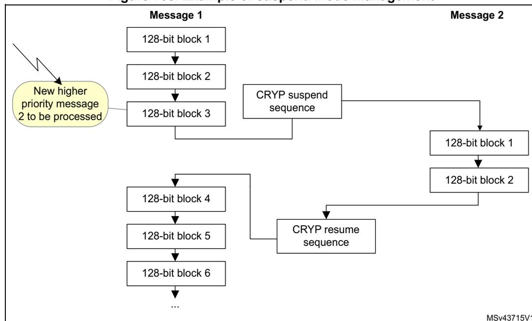
The diagram illustrates the flow of data blocks for two messages, Message 1 and Message 2, during a suspend/resume operation. Message 1 consists of 128-bit blocks 1 through 6, followed by an ellipsis. Message 2 consists of 128-bit blocks 1 and 2. A lightning bolt icon points to a yellow oval containing the text "New higher priority message 2 to be processed". This oval is positioned between Message 1's block 3 and block 4. A line from the oval points to a box labeled "CRYP suspend sequence", which in turn points to Message 2's block 1. After Message 2's block 2, a line points to a box labeled "CRYP resume sequence", which then points back to Message 1's block 4. The diagram shows that Message 1's processing is suspended after block 3, Message 2 is processed, and then Message 1 resumes at block 4.
A detailed description of suspend/resume operations can be found in each AES mode section.
20.4.10 CRYP DES/TDES basic chaining modes (ECB, CBC)
Overview
FIPS PUB 46-3 – 1999 (and ANSI X9.52-1998) provides a thorough explanation of the processing involved in the four operation modes supplied by the DES computing core: TDES-ECB encryption, TDES-ECB decryption, TDES-CBC encryption and TDES-CBC decryption. This section only gives a brief explanation of each mode.
DES/TDES-ECB encryption
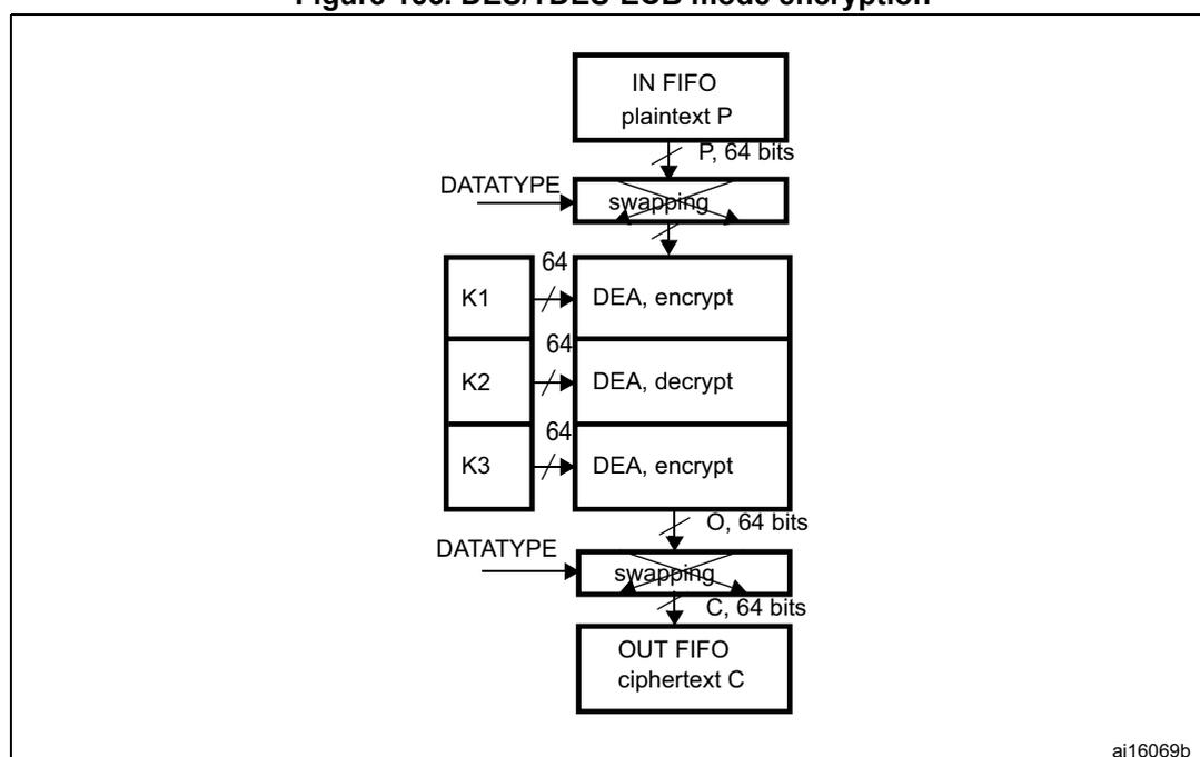
Figure 166 illustrates the encryption in DES and TDES Electronic CodeBook (DES/TDES-ECB) mode. This mode is selected by programming ALGOMODE 0x0 and ALGODIR to 0 in CRYP_CR.
Figure 166. DES/TDES-ECB mode encryption
graph TD
    P["IN FIFO
plaintext P
(P, 64 bits)"] --> S1[swapping]
    S1 --> E1["DEA, encrypt
(K1, 64 bits)"]
    E1 --> D2["DEA, decrypt
(K2, 64 bits)"]
    D2 --> E3["DEA, encrypt
(K3, 64 bits)"]
    E3 --> O["O, 64 bits"]
    O --> S2[swapping]
    S2 --> C["OUT FIFO
ciphertext C
(C, 64 bits)"]
    DATATYPE1[DATATYPE] --> S1
    DATATYPE2[DATATYPE] --> S2
- 1. K: key; C: cipher text; I: input block; O: output block; P: plain text.
A 64-bit plaintext data block (P) is used after bit/byte/half-word as the input block (I). The input block is processed through the DEA in the encrypt state using K1. The output of this process is fed back directly to the input of the DEA where the DES is performed in the decrypt state using K2. The output of this process is fed back directly to the input of the DEA where the DES is performed in the encrypt state using K3. The resultant 64-bit output block (O) is used, after bit/byte/half-word swapping, as ciphertext (C) and it is pushed into the OUT FIFO.
Note: For more information on data swapping, refer to Section 20.4.16: CRYP data registers and data swapping . Detailed DES/TDES encryption sequence can be found in Section 20.4.5: CRYP procedure to perform a cipher operation .
DES/TDES-ECB mode decryption
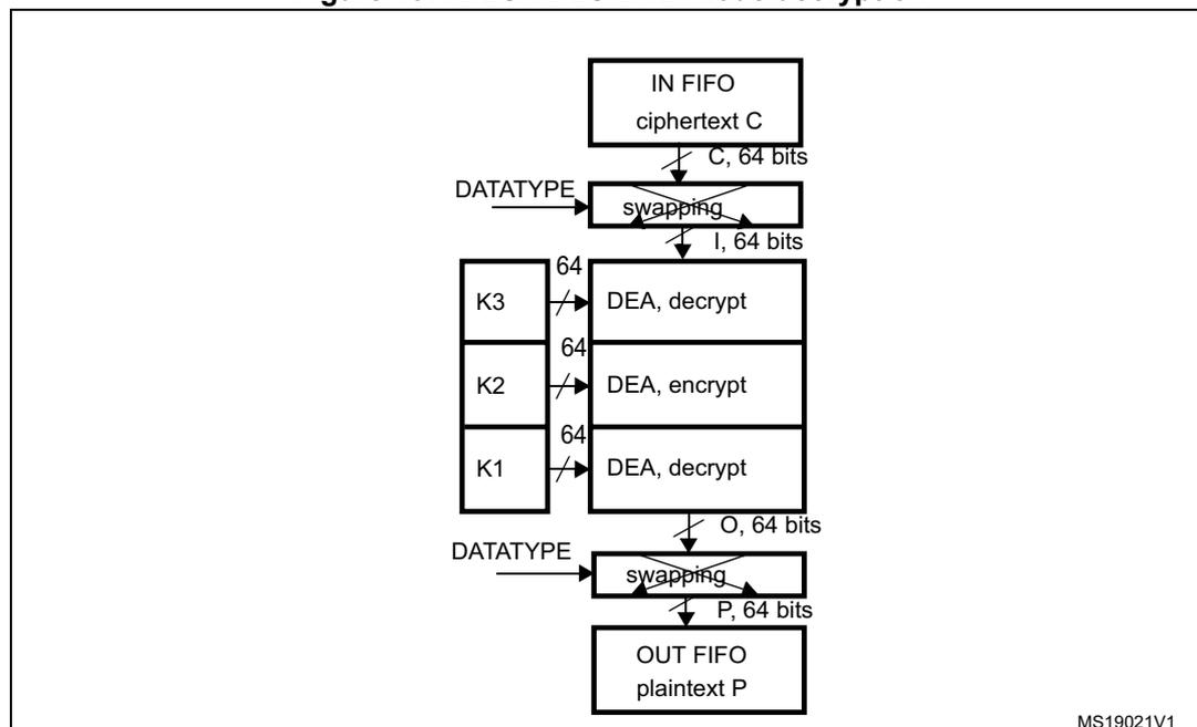
Figure 167 illustrates the decryption in DES and TDES Electronic CodeBook (DES/TDES-ECB) mode. This mode is selected by programming ALGOMODE to 0x0 and ALGODIR to 1 in CRYP_CR.
Figure 167. DES/TDES-ECB mode decryption
graph TD
    C["IN FIFO
ciphertext C
C, 64 bits"] --> S1[swapping]
    S1 --> I["I, 64 bits"]
    I --> D1["DEA, decrypt
K3"]
    D1 --> D2["DEA, encrypt
K2"]
    D2 --> D3["DEA, decrypt
K1"]
    D3 --> O["O, 64 bits"]
    O --> S2[swapping]
    S2 --> P["OUT FIFO
plaintext P
P, 64 bits"]
    DATATYPE1[DATATYPE] --> S1
    DATATYPE2[DATATYPE] --> S2
    K3["K3
64"] --> D1
    K2["K2
64"] --> D2
    K1["K1
64"] --> D3
- 1. K: key; C: cipher text; I: input block; O: output block; P: plain text.
A 64-bit ciphertext block (C) is used, after bit/byte/half-word swapping, as the input block (I). The keying sequence is reversed compared to that used in the encryption process. The input block is processed through the DEA in the decrypt state using K3. The output of this process is fed back directly to the input of the DEA where the DES is performed in the encrypt state using K2. The new result is directly fed to the input of the DEA where the DES is performed in the decrypt state using K1. The resultant 64-bit output block (O), after bit/byte/half-word swapping, produces the plaintext (P).
Note: For more information on data swapping refer to Section 20.4.16: CRYP data registers and data swapping . Detailed DES/TDES encryption sequence can be found in Section 20.4.5: CRYP procedure to perform a cipher operation .
DES/TDES-CBC encryption
Figure 168 illustrates the encryption in DES and TDES Cipher Block Chaining (DES/TDES-CBC) mode. This mode is selected by programming ALGOMODE to 0x1 and ALGODIR to 0 in CRYP_CR.
Figure 168. DES/TDES-CBC mode encryption
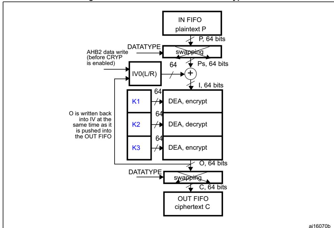
K: key; C: cipher text; I: input block; O: output block; Ps: plain text before swapping (when decoding) or after swapping (when encoding); P: plain text; IV: initialization vectors.
This mode begins by dividing a plaintext message into 64-bit data blocks. In TCBC encryption, the first input block ( \( I_1 \) ), obtained after bit/byte/half-word swapping, is formed by exclusive-ORing the first plaintext data block ( \( P_1 \) ) with a 64-bit initialization vector IV ( \( I_1 = IV \oplus P_1 \) ). The input block is processed through the DEA in the encrypt state using K1. The output of this process is fed back directly to the input of the DEA, which performs the DES in the decrypt state using K2. The output of this process is fed directly to the input of the DEA, which performs the DES in the encrypt state using K3. The resultant 64-bit output block ( \( O_1 \) ) is used directly as the ciphertext ( \( C_1 \) ), that is, \( C_1 = O_1 \) .
This first ciphertext block is then exclusive-ORed with the second plaintext data block to produce the second input block, ( \( I_2 = (C_1 \oplus P_2) \) ). Note that \( I_2 \) and \( P_2 \) now refer to the second block. The second input block is processed through the TDEA to produce the second ciphertext block.
This encryption process continues to “chain” successive cipher and plaintext blocks together until the last plaintext block in the message is encrypted.
If the message does not consist of an integral number of data blocks, then the final partial data block should be encrypted in a manner specified for the application.
Note: For more information on data swapping refer to Section 20.4.16: CRYP data registers and data swapping .
Detailed DES/TDES encryption sequence can be found in Section 20.4.5: CRYP procedure to perform a cipher operation .
DES/TDES-CBC decryption
Figure 168 illustrates the decryption in DES and TDES Cipher Block Chaining (DES/TDES-ECB) mode. This mode is selected by writing ALGOMODE to 0x1 and ALGODIR to 1 in CRYP_CR.
Figure 169. DES/TDES-CBC mode decryption
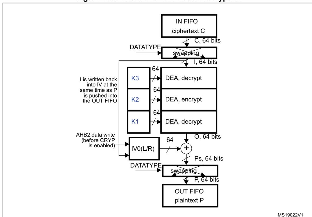
- 1. K: key; C: cipher text; I: input block; O: output block; Ps: plain text before swapping (when decoding) or after swapping (when encoding); P: plain text; IV: initialization vectors.
In this mode the first ciphertext block ( \( C_1 \) ) is used directly as the input block ( \( I_1 \) ). The keying sequence is reversed compared to that used for the encrypt process. The input block is processed through the DEA in the decrypt state using \( K_3 \) . The output of this process is fed directly to the input of the DEA where the DES is processed in the encrypt state using \( K_2 \) . This resulting value is directly fed to the input of the DEA where the DES is processed in the decrypt state using \( K_1 \) . The resulting output block is exclusive-ORed with the IV (which must be the same as that used during encryption) to produce the first plaintext block ( \( P_1 = O_1 \oplus IV \) ).
The second ciphertext block is then used as the next input block and is processed through the TDEA. The resulting output block is exclusive-ORed with the first ciphertext block to produce the second plaintext data block ( \( P_2 = O_2 \oplus C_1 \) ). Note that \( P_2 \) and \( O_2 \) refer to the second block of data.
The DES/TDES-CBC decryption process continues in this manner until the last complete ciphertext block has been decrypted.
Ciphertext representing a partial data block must be decrypted in a manner specified for the application.
Note: For more information on data swapping refer to Section 20.4.16: CRYP data registers and data swapping .
Detailed DES/TDES encryption sequence can be found in Section 20.4.5: CRYP procedure to perform a cipher operation .
DES/TDES suspend/resume operations in ECB/CBC modes
Before interrupting the current message, the user application must respect the following steps:
- 1. If DMA is used, stop the DMA transfers to the IN FIFO by clearing to 0 the DIEN bit in the CRYP_DMACR register.
- 2. Wait until both the IN and the OUT FIFOs are empty (IFEM = 1 and OFNE = 0 in the CRYP_SR) and the BUSY bit is cleared. Alternatively, as the input FIFO can contain up to four unprocessed DES blocks, the application could decide for real-time reason to interrupt the cryptographic processing without waiting for the IN FIFO to be empty. In this case, the alternative is:
- a) Wait until OUT FIFO is empty (OFNE = 0).
- b) Read back the data loaded in the IN FIFO that have not been processed and save them in the memory until the IN FIFO is empty.
- 3. If DMA is used stop the DMA transfers from the OUT FIFO by clearing to 0 the DOEN bit in the CRYP_DMACR register.
- 4. Disable the cryptographic processor by setting the CRYPTEN bit to 0 in CRYP_CR, then save the current configuration (bits [9:2] in the CRYP_CR register). If CBC mode is selected, save the initialization vector registers, since CRYP_IVx(L/R)R registers have changed from initial values during the data processing.
Note: Key registers do not need to be saved as the original key value is known by the application.
- 5. If DMA is used, save the DMA controller status (such as the pointers to IN and OUT data transfers, number of remaining bytes).
To resume message processing, the user application must respect the following sequence:
- 1. If DMA is used, reconfigure the DMA controller to complete the rest of the FIFO IN and FIFO OUT transfers.
- 2. Make sure the cryptographic processor is disabled by reading the CRYPTEN bit in CRYP_CR (it must be 0).
- 3. Configure again the cryptographic processor with the initial setting in CRYP_CR, as well as the key registers using the saved configuration.
- 4. If the CBC mode is selected, restore CRYP_IVx(L/R)R registers using the saved configuration.
- 5. Optionally, write the data that were saved during context saving into the IN FIFO.
- 6. Enable the cryptographic processor by setting the CRYPTEN bit to 1.
- 7. If DMA is used, enable again DMA requests for the cryptographic processor, by setting to 1 the DIEN and DOEN bits in the CRYP_DMACR register.
20.4.11 CRYP AES basic chaining modes (ECB, CBC)
Overview
FIPS PUB 197 (November 26, 2001) provides a thorough explanation of the processing involved in the four basic operation modes supplied by the AES computing core: AES-ECB encryption, AES-ECB decryption, AES-CBC encryption and AES-CBC decryption. This section only gives a brief explanation of each mode.
AES ECB encryption
Figure 170 illustrates the AES Electronic codebook (AES-ECB) mode encryption. This mode is selected by writing ALGOMODE to 0x4 and ALGODIR to 0 in CRYP_CR.
Figure 170. AES-ECB mode encryption
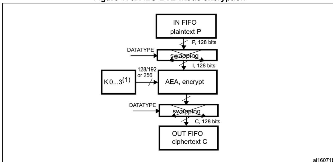
The diagram illustrates the data flow for AES-ECB mode encryption. It starts with an 'IN FIFO' containing 'plaintext P'. An arrow labeled 'P, 128 bits' points down to a 'swapping' block. A 'DATATYPE' input is shown to this block. The output of the 'swapping' block is labeled 'I, 128 bits' and points down to an 'AEA, encrypt' block. To the left of the 'AEA, encrypt' block is a key input labeled 'K0...3(1)' with a slash and '128/192 or 256' below it. The output of the 'AEA, encrypt' block points down to another 'swapping' block, which also has a 'DATATYPE' input. The output of this second 'swapping' block is labeled 'C, 128 bits' and points down to an 'OUT FIFO' containing 'ciphertext C'. The identifier 'ai16071b' is in the bottom right corner of the diagram area.
- 1. K: key; C: cipher text; I: input block; O: output block; P: plain text.
- 2. If Key size = 128: Key = [K3 K2].
If Key size = 192: Key = [K3 K2 K1].
If Key size = 256: Key = [K3 K2 K1 K0].
In this mode a 128- bit plaintext data block (P) is used after bit/byte/half-word swapping as the input block (I). The input block is processed through the AEA in the encrypt state using the 128, 192 or 256-bit key. The resultant 128-bit output block (O) is used after bit/byte/half-word swapping as ciphertext (C). It is then pushed into the OUT FIFO.
For more information on data swapping refer to Section 20.4.16: CRYP data registers and data swapping .
AES ECB decryption
Figure 171 illustrates the AES Electronic codebook (AES-ECB) mode decryption. This mode is selected by programming ALGOMODE to 0x4 and ALGODIR to 1 in CRYP_CR.
Figure 171. AES-ECB mode decryption
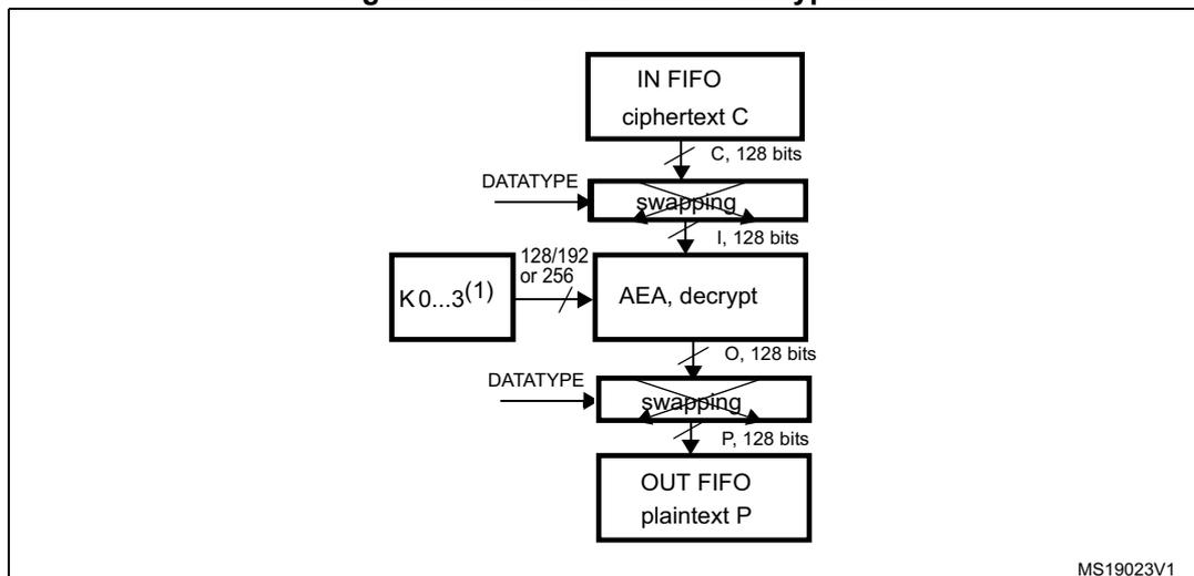
The diagram illustrates the data flow for AES-ECB decryption. It starts with an 'IN FIFO' containing 'ciphertext C'. An arrow labeled 'C, 128 bits' points from the IN FIFO to a 'swapping' block. A 'DATATYPE' input is shown to this block. The output of the swapping block is 'I, 128 bits', which points to an 'AEA, decrypt' block. A key input 'K 0...3(1)' with a bus width of '128/192 or 256' is also shown to the AEA block. The output of the AEA block is 'O, 128 bits', which points to another 'swapping' block. A 'DATATYPE' input is shown to this block. The output of this second swapping block is 'P, 128 bits', which points to an 'OUT FIFO' containing 'plaintext P'. The identifier 'MS19023V1' is located in the bottom right corner of the diagram.
- 1. K: key; C: cipher text; I: input block; O: output block; P: plain text.
- 2. If Key size = 128 => Key = [K3 K2]
If Key size = 192 => Key = [K3 K2 K1]
If Key size = 256 => Key = [K3 K2 K1 K0].
To perform an AES decryption in ECB mode, the secret key has to be prepared (it is necessary to execute the complete key schedule for encryption) by collecting the last round key, and using it as the first round key for the decryption of the ciphertext. This preparation phase is computed by the AES core. Refer to Section 20.4.7: Preparing the CRYP AES key for decryption for more details on how to prepare the key.
When the key preparation is complete, the decryption proceed as follows: a 128-bit ciphertext block (C) is used after bit/byte/half-word swapping as the input block (I). The keying sequence is reversed compared to that of the encryption process. The resultant 128-bit output block (O), after bit/byte or half-word swapping, produces the plaintext (P). The AES-CBC decryption process continues in this manner until the last complete ciphertext block has been decrypted.
For more information on data swapping refer to Section 20.4.16: CRYP data registers and data swapping .
AES CBC encryption
Figure 172 illustrates the AES Cipher block chaining (AES-CBC) mode encryption. This mode is selected by writing ALGOMODE to 0x5 and ALGODIR to 0 in CRYP_CR.
Figure 172. AES-CBC mode encryption
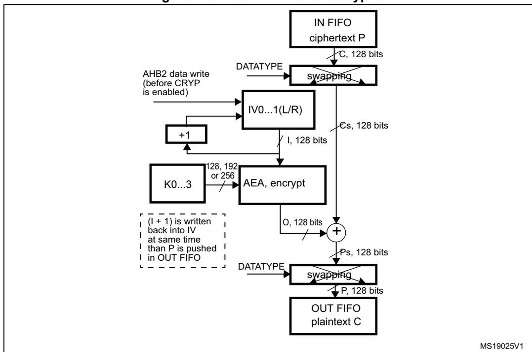
![Block diagram of AES-CBC mode encryption. The diagram shows the flow of data from an IN FIFO (plaintext P) through a swapping block (producing Ps, 128 bits), an XOR gate (combined with IV to produce I, 128 bits), an AEA (encrypt) block (producing O, 128 bits), and a second swapping block (producing C, 128 bits) into an OUT FIFO (ciphertext C). The IV is initialized to [IV1 IV0] and updated with the output O. The key K is 0...3. A dashed box indicates that O is written back into IV at the same time it is pushed into the OUT FIFO.](/RM0386-STM32F469-479/9a944fd3adaf0f59d80c06131c070324_img.jpg)
The diagram illustrates the data flow in AES-CBC encryption. Plaintext P (128 bits) is read from the IN FIFO and passes through a 'swapping' block (controlled by DATATYPE). The output is Ps (128 bits), which is then XORed with the Initialization Vector (IV) to produce the input block I (128 bits). The IV is initialized to [IV1 IV0] and updated with the output O. The input block I is processed by the AEA (encrypt) block using a key K (0...3, 128, 192, or 256 bits) to produce the output block O (128 bits). The output block O is then passed through another 'swapping' block (controlled by DATATYPE) to produce the ciphertext C (128 bits), which is written to the OUT FIFO. A dashed box indicates that the output block O is written back into the IV at the same time it is pushed into the OUT FIFO.
- 1. K: key; C: cipher text; I: input block; O: output block; Ps: plain text before swapping (when decoding) or after swapping (when encoding); P: plain text; IV: Initialization vectors.
- 2. \( IVx = [IVxR \ IVxL] \) , R = right, L = left.
- 3. If Key size = 128 => Key = [K3 K2].
If Key size = 192 => Key = [K3 K2 K1]
If Key size = 256 => Key = [K3 K2 K1 K0].
In this mode the first input block ( \( I_1 \) ) obtained after bit/byte/half-word swapping is formed by exclusive-ORing the first plaintext data block ( \( P_1 \) ) with a 128-bit initialization vector IV ( \( I_1 = IV \oplus P_1 \) ). The input block is processed through the AEA in the encrypt state using the 128-, 192- or 256-bit key ( \( K_{0..3} \) ). The resultant 128-bit output block ( \( O_1 \) ) is used directly as ciphertext ( \( C_1 \) ), that is, \( C_1 = O_1 \) . This first ciphertext block is then exclusive-ORed with the second plaintext data block to produce the second input block, \( (I_2) = (C_1 \oplus P_2) \) . Note that \( I_2 \) and \( P_2 \) now refer to the second block. The second input block is processed through the AEA to produce the second ciphertext block. This encryption process continues to “chain” successive cipher and plaintext blocks together until the last plaintext block in the message is encrypted.
If the message does not consist of an integral number of data blocks, then the final partial data block should be encrypted in a manner specified for the application, as explained in Section 20.4.8: CRYP stealing and data padding .
For more information on data swapping, refer to Section 20.4.16: CRYP data registers and data swapping .
AES CBC decryption
Figure 173 illustrates the AES Cipher block chaining (AES-CBC) mode decryption. This mode is selected by writing ALGOMODE to 0x5 and ALGODIR to 1 in CRYP_CR.
Figure 173. AES-CBC mode decryption
![Block diagram of AES-CBC mode decryption. The process starts with ciphertext C (128 bits) from an IN FIFO. This is processed through a 'swapping' block (controlled by DATATYPE) to produce an input block I (128 bits). I is then processed by the AEA (decrypt) block using a key K (128, 192, or 256 bits, represented as K0...3). The output of the AEA is an output block O (128 bits). O is XORed with the Initialization Vector IV (IV = [IVxR IVxL], 128 bits) to produce the plaintext before swapping, Ps (128 bits). Ps is then processed through another 'swapping' block (controlled by DATATYPE) to produce the final plaintext P (128 bits), which is pushed into an OUT FIFO. A dashed box indicates that I is written back into IV at the same time P is pushed into the OUT FIFO. An AHB2 data write (before CRYP is enabled) is shown to the IV register.](/RM0386-STM32F469-479/668faf98604cdde4b3ce5770d2f0f19c_img.jpg)
MS19024V1
- 1. K: key; C: cipher text; I: input block; O: output block; Ps: plain text before swapping (when decoding) or after swapping (when encoding); P: plain text; IV: Initialization vectors.
- 2. \( IVx = [IVxR \ IVxL] \) , R = right, L = left.
- 3. If Key size = 128 => Key = [K3 K2].
If Key size = 192 => Key = [K3 K2 K1].
If Key size = 256 => Key = [K3 K2 K1 K0].
In CBC mode, like in ECB mode, the secret key must be prepared to perform an AES decryption. Refer to Section 20.4.7: Preparing the CRYP AES key for decryption for more details on how to prepare the key.
When the key preparation process is complete, the decryption proceeds as follows: the first 128-bit ciphertext block ( \( C_1 \) ) is used directly as the input block ( \( I_1 \) ). The input block is processed through the AEA in the decrypt state using the 128-, 192- or 256-bit key. The resulting output block is exclusive-ORed with the 128-bit initialization vector IV (which must be the same as that used during encryption) to produce the first plaintext block ( \( P_1 = O_1 \oplus IV \) ).
The second ciphertext block is then used as the next input block and is processed through the AEA. The resulting output block is exclusive-ORed with the first ciphertext block to produce the second plaintext data block ( \( P_2 = O_2 \oplus C_1 \) ). Note that \( P_2 \) and \( O_2 \) refer to the second block of data. The AES-CBC decryption process continues in this manner until the last complete ciphertext block has been decrypted.
Ciphertext representing a partial data block must be decrypted in a manner specified for the application, as explained in Section 20.4.8: CRYP stealing and data padding .
For more information on data swapping, refer to Section 20.4.16: CRYP data registers and data swapping .
AES suspend/resume operations in ECB/CBC modes
Before interrupting the current message, the user application must respect the following sequence:
- 1. If DMA is used, stop the DMA transfers to the IN FIFO by clearing to 0 the DIEN bit in the CRYP_DMACR register.
- 2. Wait until both the IN and the OUT FIFOs are empty (IFEM = 1 and OFNE = 0 in the CRYP_SR) and the BUSY bit is cleared.
- 3. If DMA is used, stop the DMA transfers from the OUT FIFO by clearing to 0 the DOEN bit in the CRYP_DMACR register.
- 4. Disable the CRYP by setting the CRYPTEN bit to 0 in CRYP_CR, then save the current configuration (bits [9:2] in the CRYP_CR register). If ECB mode is not selected, save the initialization vector registers, because CRYP_IVx(L/R)R registers have changed from initial values during the data processing.
Note: Key registers do not need to be saved as the original key value is known by the application.
- 5. If DMA is used, save the DMA controller status (such as pointers to IN and OUT data transfers, number of remaining bytes).
To resume message processing, the user application must respect the following sequence:
- 1. If DMA is used, reconfigure the DMA controller to complete the rest of the FIFO IN and FIFO OUT transfers.
- 2. Make sure the cryptographic processor is disabled by reading the CRYPTEN bit in CRYP_CR (it must be set to 0).
- 3. Configure the cryptographic processor again with the initial setting in CRYP_CR, as well as the key registers using the saved configuration.
- 4. For AES-ECB or AES-CBC decryption, the key must be prepared again, as described in Section 20.4.7: Preparing the CRYP AES key for decryption .
- 5. If ECB mode is not selected, restore CRYP_IVx(L/R)R registers using the saved configuration.
- 6. Enable the cryptographic processor by setting the CRYPTEN bit to 1.
- 7. If DMA is used, enable again the DMA requests from the cryptographic processor, by setting DIEN and DOEN bits to 1 in the CRYP_DMACR register.
20.4.12 CRYP AES counter mode (AES-CTR)
Overview
The AES counter mode (CTR) uses the AES block as a key stream generator. The generated keys are then XORed with the plaintext to obtain the ciphertext.
CTR chaining is defined in NIST Special Publication 800-38A, Recommendation for Block Cipher Modes of Operation . A typical message construction in CTR mode is given in Figure 174 .
Figure 174. Message construction for the Counter mode
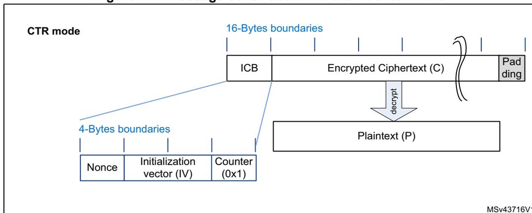
The diagram shows the structure of a message in CTR mode. At the top, a long horizontal bar represents the message, divided into three main parts: an Initial Counter Block (ICB), Encrypted Ciphertext (C), and Padding. Above this bar, vertical lines indicate '16-Bytes boundaries'. Below the ICB, a callout box shows its internal structure: Nonce, Initialization vector (IV), and Counter (0x1). Above this callout, vertical lines indicate '4-Bytes boundaries'. A downward arrow labeled 'decrypt' points from the Encrypted Ciphertext (C) to a box labeled Plaintext (P). A curly brace on the right side of the ciphertext groups it with the padding. The identifier 'MSV43716V1' is in the bottom right corner.
The structure of this message is as below:
- • A 16-byte Initial Counter Block (ICB), composed of three distinct fields:
- – A nonce : a 32-bit, single-use value (i.e. a new nonce should be assigned to each new communication).
- – The initialization vector (IV) : a 64-bit value that must be unique for each execution of the mode under a given key.
- – The counter : a 32-bit big-endian integer that is incremented each time a block has been processed. The initial value of the counter should be set to 1.
- • The plaintext (P) is both authenticated and encrypted as ciphertext C, with a known length. This length can be non-multiple of 16 bytes, in which case a plaintext padding is required.
AES CTR processing
Figure 175 (respectively Figure 176) describes the AES-CTR encryption (respectively decryption) process implemented within this peripheral. This mode is selected by programming ALGOMODE bitfield to 0x6 in CRYP_CR.
Figure 175. AES-CTR mode encryption
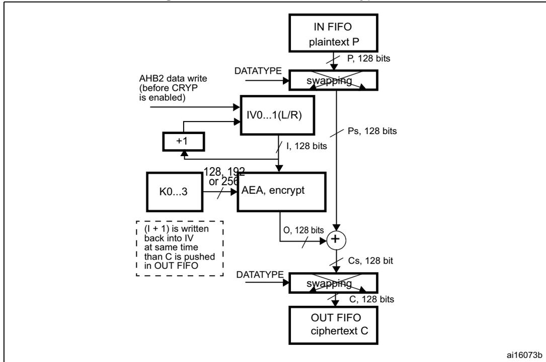
The diagram illustrates the AES-CTR mode encryption process. Data flows from the IN FIFO plaintext P (128 bits) through a swapping block (controlled by DATATYPE ) to become Ps, 128 bits . Simultaneously, an Initialization vector (I, 128 bits) is provided to the AEA, encrypt block along with a key (K0...3) (128, 192, or 256 bits). The AEA, encrypt block produces an output O, 128 bits . This output is XORed ( + ) with Ps, 128 bits to generate Cs, 128 bit (cipher text after swapping when decoding, or before swapping when encoding). Cs, 128 bit is then passed through another swapping block (controlled by DATATYPE ) to become C, 128 bits (cipher text) and is pushed into the OUT FIFO ciphertext C . A feedback loop from the output of the XOR operation goes through a +1 block and back to the I input of the AEA, encrypt block. A dashed box indicates that (I + 1) is written back into IV at the same time C is pushed in OUT FIFO . An AHB2 data write (before CRYP is enabled) is also shown.
- 1. K: key; C: cipher text; I: input Block; o: output block; Ps: plain text before swapping (when decoding) or after swapping (when encoding); Cs: cipher text after swapping (when decoding) or before swapping (when encoding); P: plain text; IV: Initialization vectors.
Figure 176. AES-CTR mode decryption
- 1. K: key; C: cipher text; I: input Block; o: output block; Ps: plain text before swapping (when decoding) or after swapping (when encoding); Cs: cipher text after swapping (when decoding) or before swapping (when encoding); P: plain text; IV: Initialization vectors.
In CTR mode, the output block is XORed with the subsequent input block before it is input to the algorithm. Initialization vectors in the peripheral must be initialized as shown on Table 142 .
Table 142. Counter mode initialization vector
| CRYP_IV1RR[31:0] | CRYP_IV1LR[31:0] | CRYP_IV0RR[31:0] | CRYP_IV0LR[31:0] |
|---|---|---|---|
| IVI[127:96] | IVI[95:64] | IVI[63:32] | IVI[31:0] 32-bit counter = 0x1 |
Unlike in CBC mode, which uses the CRYP_IVx(L/R)R registers only once when processing the first data block, in CTR mode IV registers are used for processing each data block, and the peripheral increments the least significant 32 bits (leaving the other most significant 96 bits unchanged).
CTR decryption does not differ from CTR encryption, since the core always encrypts the current counter block to produce the key stream that will be XORed with the plaintext or cipher as input. Thus when ALGOMODE is set to 0x6, ALGODIR is don't care.
Note: In this mode the key must NOT be prepared for decryption.
The following sequence must be used to perform an encryption or a decryption in CTR chaining mode:
- 1. Make sure the cryptographic processor is disabled by clearing the CRYPTEN bit in the CRYP_CR register.
- 2. Configure CRYP_CR as follows:
- a) Program ALGOMODE bits to 0x6 to select CTR mode. ALGODIR can be set to any value.
- b) Configure the data type (1, 8, 16 or 32 bits) through the DATATYPE bits.
- c) Define the key length using KEYSIZE bits.
- 3. Initialize the key registers (128, 192 or 256 bits) in CRYP_KEYRx as well as the initialization vector (IV) as described in Table 142 .
- 4. Flush the IN and OUT FIFOs by writing the FFLUSH bit to 1 in the CRYP_CR register.
- 5. If it is the last block, optionally pad the data with zeros to have a complete block.
- 6. Append data in the cryptographic processor and read the result. The three possible scenarios are described in Section 20.4.5: CRYP procedure to perform a cipher operation .
- 7. Repeat the previous step until the second last block is processed. For the last block, execute the two previous steps. For this last block, the driver must discard the data that is not part of the data when the last block size is less than 16 bytes.
Suspend/resume operations in CTR mode
Like for the CBC mode, it is possible to interrupt a message to send a higher priority message, and resume the message which was interrupted. Detailed CBC sequence can be found in Section 20.4.11: CRYP AES basic chaining modes (ECB, CBC) .
Note: Like for CBC mode, IV registers must be reloaded during the resume operation.
20.4.13 CRYP AES Galois/counter mode (GCM)
Overview
The AES Galois/counter mode (GCM) allows encrypting and authenticating the plaintext, and generating the correspondent ciphertext and tag (also known as message authentication code). To ensure confidentiality, GCM algorithm is based on AES counter mode. It uses a multiplier over a fixed finite field to generate the tag.
GCM chaining is defined in NIST Special Publication 800-38D, Recommendation for Block Cipher Modes of Operation - Galois/Counter Mode (GCM) and GMAC . A typical message construction in GCM mode is given in Figure 177 .
Figure 177. Message construction for the Galois/counter mode
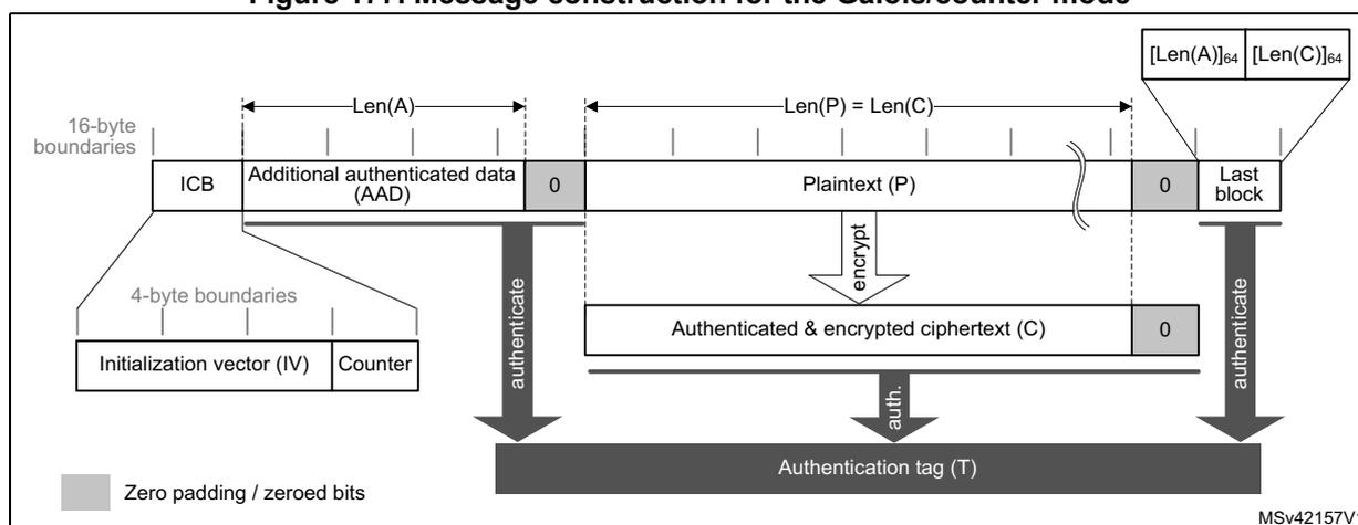
The diagram shows the structure of a GCM message. It starts with a 16-byte Initial Counter Block (ICB), which is composed of a 96-bit Initialization vector (IV) and a 32-bit Counter. This is followed by Additional authenticated data (AAD) of length \( Len(A) \) . The AAD is followed by a 0 (zero padding). The next part is the Plaintext (P) of length \( Len(P) = Len(C) \) . The Plaintext is encrypted to produce the Authenticated & encrypted ciphertext (C). The ciphertext is followed by a 0 (zero padding). The last block is the Last block, which contains the length of A (on 64 bits) and the length of ciphertext C (on 64 bits), denoted as \( [Len(A)]_{64} \) and \( [Len(C)]_{64} \) . The entire message is authenticated to produce the Authentication tag (T). The diagram also shows the flow of data: ICB is used for encryption and authentication; AAD is used for authentication; Plaintext is encrypted to C and also used for authentication; C is used for authentication; and the Last block is used for authentication. The legend indicates that grey boxes represent zero padding / zeroed bits.
The structure of this message is defined as below:
- • A 16-byte Initial Counter Block (ICB), composed of two distinct fields:
- – The initialization vector (IV): a 96-bit value that must be unique for each execution of the mode under a given key. Note that the GCM standard supports IV that are shorter than 96-bit, but in this case strict rules apply.
- – The counter : a 32-bit big-endian integer that is incremented each time a block has been processed. According to NIST specification, the counter value is 0x2 when processing the first block of payload.
- • The authenticated header A (also known as Additional Authentication Data) has a known length \( Len(A) \) that can be non-multiple of 16 bytes and cannot exceed \( 2^{64}-1 \) bits. This part of the message is only authenticated, not encrypted.
- • The plaintext message (P) is both authenticated and encrypted as ciphertext C, with a known length \( Len(P) \) that can be non-multiple of 16 bytes, and cannot exceed \( 2^{32}-2 \) blocks of 128-bits.
Note: GCM standard specifies that ciphertext C has same bit length as the plaintext P.
- • When a part of the message (AAD or P) has a length which is non-multiple of 16 bytes, a special padding scheme is required.
- • The last block is composed of the length of A (on 64 bits) and the length of ciphertext C (on 64 bits) as shown in Table 143 .
Table 143. GCM last block definition
| Endianness | Bit[0] | Bit[32] | Bit[64] | Bit[96] |
|---|---|---|---|---|
| Input data | 0x0 | Header length[31:0] | 0x0 | Payload length[31:0] |
AES GCM processing
This mode is selected by writing ALGOMODE bitfield to 0x6 in CRYP_CR.
The mechanism for the confidentiality of the plaintext in GCM mode is a variation of the Counter mode, with a particular 32-bit incrementing function that generates the necessary sequence of counter blocks.
CRYP_IVx(L/R)R registers are used for processing each data block. The cryptographic processor automatically increments the 32 least significant bits of the counter block. The first counter block (CB1) written by the application is equal to the Initial Counter Block incremented by one (see Table 144 ).
Table 144. GCM mode IV registers initialization
| Register | CRYP_IV0LR[31:0] | CRYP_IV0RR[31:0] | CRYP_IV1LR[31:0] | CRYP_IV1RR[31:0] |
|---|---|---|---|---|
| Input data | ICB[127:96] | ICB[95:64] | ICB[63:32] | ICB[31:0] 32-bit counter = 0x2 |
Note: In this mode the key must NOT be prepared for decryption.
The authentication mechanism in GCM mode is based on a hash function, called GF2mul , that performs multiplication by a fixed parameter, called the hash subkey (H), within a binary Galois field.
To process a GCM message, the driver must go through four phases, which are described in the following subsections.
- • The Init phase: the peripheral prepares the GCM hash subkey (H) and performs the IV processing
- • The Header phase: the peripheral processes the Additional Authenticated Data (AAD), with hash computation only.
- • The Payload phase: the peripheral processes the plaintext (P) with hash computation, keystream encryption and data XORing. It operates in a similar way for ciphertext (C).
- • The Final phase: the peripheral generates the authenticated tag (T) using the data last block.
1. GCM initialization phase
During this first step, the GCM hash subkey (H) is calculated and saved internally to be used for processing all the blocks. It is recommended to follow the sequence below:
- a) Make sure the cryptographic processor is disabled by clearing the CRYPTEN bit in the CRYP_CR register.
- b) Select the GCM chaining mode by programming ALGOMODE bits to 0x8 in CRYP_CR. In the same register define the key length using KEYSIZE bits and the data type using DATATYPE bits.
- c) Configure GCM_CCMPH bits to 0b00 in CRYP_CR to indicate that the initialization phase is ongoing.
- d) Initialize the key registers (128, 192 or 256 bits) in CRYP_KEYRx as well as the initialization vector (IV) as defined in Table 144 .
- e) Set CRYPTEN bit to 1 to start the calculation of the hash key.
- f) Wait for the CRYPTEN bit to be cleared to 0 by the cryptographic processor, before moving on to the next phase.
2. GCM header phase
The below sequence shall be performed after the GCM initialization phase. It must be complete before jumping to the payload phase. The sequence is identical for encryption and decryption.
- g) Set the GCM_CCMPH bits to 0b01 in CRYP_CR to indicate that the header phase is ongoing.
- h) Set the CRYPTEN bit to 1 to start accepting data.
- i) If it is the last block of additional authenticated data, optionally pad the data with zeros to have a complete block.
- j) Append additional authenticated data in the cryptographic processor. The three possible scenarios are described in Section 20.4.5: CRYP procedure to perform a cipher operation .
- k) Repeat the previous step until the second last additional authenticated data block is processed. For the last block, execute the two previous steps. Once all the additional authenticated data have been supplied, wait until the BUSY flag is cleared before moving on to the next phase.
Note: This phase can be skipped if there is no additional authenticated data, i.e. Len(A) = 0.
In header and payload phases, CRYPTEN bit is not automatically cleared by the cryptographic processor.
3. GCM payload phase (encryption or decryption)
When the payload size is not null, this sequence must be executed after the GCM header phase. During this phase, the encrypted/decrypted payload is stored in the CRYP_DOUT register.
- l) Set the CRYPTEN bit to 0.
- m) Configure GCM_CCMPH to 0b10 in the CRYP_CR register to indicate that the payload phase is ongoing.
- n) Select the algorithm direction (0 for encryption, 1 for decryption) through the ALGODIR bit in CRYP_CR.
- o) Set the CRYPTEN bit to 1 to start accepting data.
- p) If it is the last block of cleartext or plaintext, optionally pad the data with zeros to have a complete block. For encryption, refer to Section 20.4.8: CRYP stealing and data padding for more details.
- q) Append payload data in the cryptographic processor, and read the result. The three possible scenarios are described in Section 20.4.5: CRYP procedure to perform a cipher operation .
- r) Repeat the previous step until the second last plaintext block is encrypted or until the last block of ciphertext is decrypted. For the last block of plaintext (encryption only), execute the two previous steps. For the last block, the driver must discard the bits that are not part of the cleartext or the ciphertext when the last block size is less than 16 bytes. Once all payload data have been supplied, wait until the BUSY flag is cleared.
Note: This phase can be skipped if there is no payload data, i.e. Len(C) = 0 (see GMAC mode).
4. GCM final phase
In this last step, the cryptographic processor generates the GCM authentication tag and stores it in CRYP_DOUT register.
- s) Configure GCM_CCMPH[1:0] to 0b11 in CRYP_CR to indicate that the Final phase is ongoing. Set the ALGODIR bit to 0 in the same register.
- t) Write the input to the CRYP_DIN register four times. The input must be composed of the length in bits of the additional authenticated data (coded on 64 bits) concatenated with the length in bits of the payload (coded of 64 bits), as show in Table 143 .
Note: In this final phase data have to be swapped according to the DATATYPE programmed in CRYP_CR register.
- u) Wait until the OFNE flag (FIFO output not empty) is set to 1 in the CRYP_SR register.
- v) Read the CRYP_DOUT register four times: the output corresponds to the authentication tag.
- w) Disable the cryptographic processor (CRYPTEN bit = 0 in CRYP_CR)
- x) If an authenticated decryption is being performed, compare the generated tag with the expected tag passed with the message.
Suspend/resume operations in GCM mode
Before interrupting the current message in header or payload phase, the user application must respect the following sequence:
- 1. If DMA is used, stop DMA transfers to the IN FIFO by clearing to 0 the DIEN bit in the CRYP_DMACR register.
- 2. Wait until both the IN and the OUT FIFOs are empty (IFEM = 1 and OFNE = 0 in the CRYP_SR register) and the BUSY bit is cleared.
- 3. If DMA is used, stop DMA transfers from the OUT FIFO by clearing to 0 the DOEN bit in the CRYP_DMACR register.
- 4. Disable the cryptographic processor by setting the CRYPTEN bit to 0 in CRYP_CR, then save the current configuration (bits [9:2], bits [17:16] and bits 19 of the CRYP_CR register). In addition, save the initialization vector registers, since CRYP_IVx(L/R)R registers have changed from their initial values during data processing.
Note: Key registers do not need to be saved as original their key value is known by the application.
- 5. Save context swap registers: CRYP_CSGCMCCM0..7R and CRYP_CSGCM0..7R
- 6. If DMA is used, save the DMA controller status (pointers to IN and OUT data transfers, number of remaining bytes, etc.).
To resume message processing, the user must respect the following sequence:
- 1. If DMA is used, reconfigure the DMA controller to complete the rest of the FIFO IN and FIFO OUT transfers.
- 2. Make sure the cryptographic processor is disabled by reading the CRYPTEN bit in CRYP_CR (it must be 0).
- 3. Configure again the cryptographic processor with the initial setting in CRYP_CR, as well as the key registers using the saved configuration.
- 4. Restore context swap registers: CRYP_CSGCMCCM0..7R and CRYP_CSGCM0..7R
- 5. Restore CRYP_IVx(L/R)R registers using the saved configuration.
- 6. Enable the cryptographic processor by setting the CRYPTEN bit to 1.
- 7. If DMA is used, enable again cryptographic processor DMA requests by setting to 1 the DIEN and DOEN bits in the CRYP_DMACR register.
Note: In Header phase, DMA OUT FIFO transfer is not used.
20.4.14 CRYP AES Galois message authentication code (GMAC)
Overview
The Galois message authentication code (GMAC) allows authenticating a plaintext and generating the corresponding tag information (also known as message authentication code). It is based on GCM algorithm, as defined in NIST Special Publication 800-38D, Recommendation for Block Cipher Modes of Operation - Galois/Counter Mode (GCM) and GMAC .
A typical message construction in GMAC mode is given in Figure 178 .
Figure 178. Message construction for the Galois Message Authentication Code mode
![Diagram illustrating the message construction for the Galois Message Authentication Code (GMAC) mode. The diagram shows a sequence of blocks: ICB (Initialization Counter Block), Authenticated data, and Last block. The ICB is split into an Initialization vector (IV) and a Counter. The Authenticated data is split into blocks of 16-byte boundaries. The Last block is split into a 0 (zero padding) and a Last block. The length of the authenticated data is indicated by Len(A). The diagram also shows the generation of an Authentication tag (T) from the ICB and the Authenticated data. A callout box shows the structure of the Last block: [Len(A)]64 and [0]64. A legend indicates that grey blocks represent zero padding. The diagram is labeled MSv42158V2.](/RM0386-STM32F469-479/147e4a98f344bbb90705d0f57d8a07e4_img.jpg)
The diagram illustrates the message construction for GMAC. It shows a sequence of blocks: ICB (Initialization Counter Block), Authenticated data, and Last block. The ICB is split into an Initialization vector (IV) and a Counter. The Authenticated data is split into blocks of 16-byte boundaries. The Last block is split into a 0 (zero padding) and a Last block. The length of the authenticated data is indicated by Len(A). The diagram also shows the generation of an Authentication tag (T) from the ICB and the Authenticated data. A callout box shows the structure of the Last block: [Len(A)] 64 and [0] 64 . A legend indicates that grey blocks represent zero padding. The diagram is labeled MSv42158V2.
AES GMAC processing
This mode is selected by writing ALGOMODE bitfield to 0x6 in CRYP_CR.
GMAC algorithm corresponds to the GCM algorithm applied on a message composed only of an header. As a consequence, all steps and settings are the same as in GCM mode, except that the payload phase (3) is not used.
Suspend/resume operations in GMAC
GMAC is exactly the same as GCM algorithm except that only header phase (2) can be interrupted.
20.4.15 CRYP AES Counter with CBC-MAC (CCM)
Overview
The AES Counter with Cipher Block Chaining-Message Authentication Code (CCM) algorithm allows encrypting and authenticating the plaintext, and generating the correspondent ciphertext and tag (also known as message authentication code). To ensure confidentiality, CCM algorithm is based on AES counter mode. It uses Cipher Block Chaining technique to generate the message authentication code. This is commonly called CBC-MAC
Note: NIST does not approve this CBC-MAC as an authentication mode outside of the context of the CCM specification.
CCM chaining is specified in NIST Special Publication 800-38C, Recommendation for Block Cipher Modes of Operation - The CCM Mode for Authentication and Confidentiality . A typical message construction in CCM mode is given in Figure 179
Figure 179. Message construction for the Counter with CBC-MAC mode
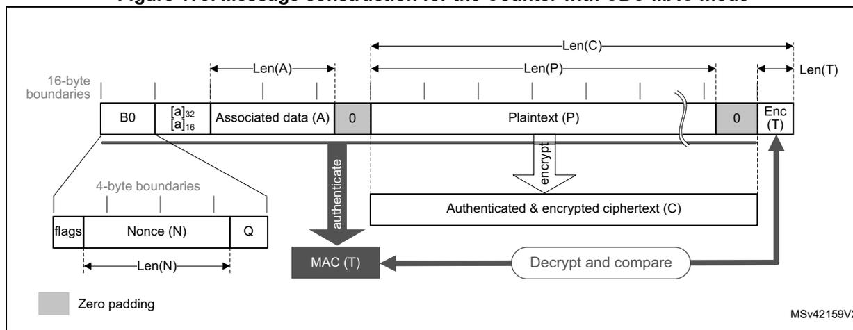
The diagram illustrates the message construction for the Counter with CBC-MAC mode. The top row shows 16-byte boundaries. The message starts with block B0, followed by Associated data (A) with length Len(A), and Plaintext (P) with length Len(P). Zero padding is applied to align fields to 16-byte boundaries. Block B0 is further divided into 4-byte boundaries containing 'flags', 'Nonce (N)' with length Len(N), and 'Q'. The 'Associated data (A)' and 'Plaintext (P)' are processed through an 'authenticate' step to produce 'MAC (T)'. The 'Plaintext (P)' is also processed through an 'encrypt' step to produce 'Authenticated & encrypted ciphertext (C)'. The final block is 'Enc (T)'. A 'Decrypt and compare' process links the ciphertext and MAC.
The structure of this message is as below:
- • One 16-byte first authentication block (called B0 by the standard), composed of three distinct fields:
- – Q: a bit string representation of the byte length of P ( Plen )
- – A nonce (N): single-use value (i.e. a new nonce should be assigned to each new communication). Size of nonce Nlen + size of Plen shall be equal to 15 bytes.
- – Flags: most significant byte containing four flags for control information, as specified by the standard. It contains two 3-bit strings to encode the values t (MAC length expressed in bytes) and q (plaintext length such as \( Plen < 2^{8q} \) bytes). Note that the counter blocks range associated to q is equal to \( 2^{8q-4} \) , i.e. if q maximum value is 8, the counter blocks used in cipher shall be on 60 bits.
Note: The cryptographic peripheral can only manage padded plaintext/ciphertext messages of length \( Plen < 2^{36} + 1 \) bytes.
- • 16-bytes blocks (B) associated to the Associated Data (A).
This part of the message is only authenticated, not encrypted. This section has a known length, ALen , that can be a non-multiple of 16 bytes (see Figure 179 ). The standard also states that, on the MSB bits of the first message block (B1), the associated data length expressed in bytes ( a ) must be encoded as defined below:
- – If \( 0 < a < 2^{16}-2^8 \) , then it is encoded as \( [a]_{16} \) , i.e. two bytes.
- – If \( 2^{16}-2^8 < a < 2^{32} \) , then it is encoded as 0xff || 0xfe || \( [a]_{32} \) , i.e. six bytes.
- – If \( 2^{32} < a < 2^{64} \) , then it is encoded as 0xff || 0xff || \( [a]_{64} \) , i.e. ten bytes.
- • 16-byte blocks (B) associated to the plaintext message (P), which is both authenticated and encrypted as ciphertext C, with a known length of PLen . This length can be a non-multiple of 16 bytes (see Figure 179 ) but cannot exceed \( 2^{32} \) blocks of 128-bit.
- • The encrypted MAC (T) of length TLen appended to the ciphertext C of overall length Clen .
- • When a part of the message (A or P) has a length which is a non-multiple of 16 bytes, a special padding scheme is required.
Note: CCM chaining mode can also be used with associated data only (i.e. no payload).
As an example, the C.1 section in NIST Special Publication 800-38C gives the following:
N:
10111213 141516
(Nlen = 56 bits or 0x7 bytes)
A:
00010203 04050607
(ALen = 64 bits or 0x8 bytes)
P:
20212223
(PLen = 32 bits i.e. Q = 0x4 bytes)
T:
6084341b
(TLen = 32 bits or t = 4)
B0:
4f101112 13141516
00000000 00000004
B1: 0008
0001 02030405 0607
0000 00000000
B2:
20212223
00000000 00000000 00000000
CTR0: 07
10111213 141516
00000000 00000000
CTR1: 07
10111213 141516
00000000 00000001
The usage of control blocks CTRx is explained in the following section. The generation of CTR0 from the first block (B0) must be managed by software.
AES CCM processing
This mode is selected by writing ALGOMODE bitfield to 0x9 in CRYP_CR.
The data input to the generation-encryption process are a valid nonce, a valid payload string, and a valid associated data string, all properly formatted. The CBC chaining mechanism is applied to the formatted data to generate a MAC, whose length is known. Counter mode encryption, which requires a sufficiently long sequence of counter blocks as input, is applied to the payload string and separately to the MAC. The resulting data, called the ciphertext C, is the output of the generation-encryption process on plaintext P.
CRYP_IVx(L/R)R registers are used for processing each data block. The cryptographic processor automatically increments the CTR counter with a bit length defined by the first block (B0). The first counter written by application, CTR1, is equal to B0 with the first 5 bits zeroed and the most significant bits containing P byte length also zeroed, then incremented by one (see Table 145 ).
Table 145. CCM mode IV registers initialization
| Register | CRYP_IV0LR[31:0] | CRYP_IV0RR[31:0] | CRYP_IV1LR[31:0] | CRYP_IV1RR[31:0] |
|---|---|---|---|---|
| Input data | B0[127:96], where the 5 most significant bits are set to 0 (flag bits) | B0[95:64] | B0[63:32] | B0[31:0], where Q length bits are set to 0, except for bit 0 that is set to 1 |
Note: In this mode, the key must NOT be prepared for decryption.
To process a CCM message, the driver must go through four phases, which are described below.
- • The Initialization phase : the peripheral processes the first block and prepares the first counter block.
- • The Header phase : the peripheral processes the Associated data (A), with hash computation only.
- • The Payload phase : the peripheral processes the plaintext (P), with hash computation, counter block encryption and data XORing. It operates in a similar way for ciphertext (C).
- • The Final phase : the peripheral generates the message authentication code (MAC).
1. CCM initialization phase
In this first step, the first block (B0) of the CCM message is programmed into the CRYP_DIN register. During this phase, the CRYP_DOUT register does not contain any output data. It is recommended to follow the sequence below:
- Make sure that the cryptographic processor is disabled by clearing the CRYPTEN bit in the CRYP_CR register.
- Select the CCM chaining mode by programming the ALGOMODE bits to 0x9 in the CRYP_CR register. In the same register define the key length using KEYSIZE bits and the data type using DATATYPE bits.
- Configure the GCM_CCMPH bits to 0b00 in CRYP_CR to indicate that we are in the initialization phase.
- Initialize the key registers (128, 192 or 256 bits) in CRYP_KEYRx as well as the initialization vector (IV) with CTR1 information, as defined in Table 145 .
- Set the CRYPTEN bit to 1 in CRYP_CR to start accepting data.
- Write the B0 packet into CRYP_DIN register, then wait for the CRYPTEN bit to be cleared to 0 by the cryptographic processor before moving on to the next phase.
Note: In this initialization phase data have to be swapped according to the DATATYPE programmed in CRYP_CR register.
2. CCM header phase
The below sequence shall be performed after the CCM initialization phase. It must be complete before jumping to the payload phase. The sequence is identical for encryption and decryption. During this phase, the CRYP_DOUT register does not contain any output data.
- Set the GCM_CCMPH bit to 0b01 in CRYP_CR to indicate that the header phase is ongoing.
- Set the CRYPTEN bit to 1 to start accepting data.
- If it is the last block of associated data, optionally pad the data with zeros to have a complete block.
- Append the associated data in the cryptographic processor. The three possible scenarios are described in Section 20.4.5: CRYP procedure to perform a cipher operation .
- Repeat the previous step until the second last associated data block is processed. For the last block, execute the two previous steps. Once all the additional authenticated data have been supplied, wait until the BUSY flag is cleared.
Note: This phase can be skipped if there is no associated data (Alen = 0).
The first block of the associated data B1 must be formatted with the associated data length.
This task must be managed by the driver.
3. CCM payload phase (encryption or decryption)
When the payload size is not null, this sequence must be performed after the CCM header phase. During this phase, the encrypted/decrypted payload is stored in the CRYP_DOUT register.
- l) Set the CRYPTEN bit to 0.
- m) Configure GCM_CCMPH bits to 0b10 in CRYP_CR to indicate that the payload phase is ongoing.
- n) Select the algorithm direction (0 for encryption, 1 for decryption) through the ALGODIR bit in CRYP_CR.
- o) Set the CRYPTEN bit to 1 to start accepting data.
- p) If it is the last block of cleartext, optionally pad the data with zeros to have a complete block (encryption only). For decryption, refer to Section 20.4.8: CRYP stealing and data padding for more details.
- q) Append payload data in the cryptographic processor, and read the result. The three possible scenarios are described in Section 20.4.5: CRYP procedure to perform a cipher operation .
- r) Repeat the previous step until the second last plaintext block is encrypted or until the last block of ciphertext is decrypted. For the last block of plaintext (encryption only), execute the two previous steps. For the last block of ciphertext (decryption only), the driver must discard the data that is not part of the cleartext when the last block size is less than 16 bytes. Once all payload data have been supplied, wait until the BUSY flag is cleared
Note: This phase can be skipped if there is no payload data, i.e. Plen = 0 or Clen = Tlen
Note: Do not forget to remove \( LSB_{Tlen}(C) \) encrypted tag information when decrypting ciphertext C.
4. CCM final phase
In this last step, the cryptographic processor generates the CCM authentication tag and stores it in the CRYP_DOUT register.
- s) Configure GCM_CCMPH[1:0] bits to 0b11 in CRYP_CR to indicate that the final phase is ongoing and set the ALGODIR bit to 0 in the same register.
- t) Load in CRYP_DIN, the CTR0 information which is described in Table 145 with bit[0] set to 0.
Note: In this final phase, data have to be swapped according to the DATATYPE programmed in CRYP_CR register.
- u) Wait until the OFNE flag (FIFO output not empty) is set to 1 in the CRYP_SR register.
- v) Read the CRYP_DOUT register four times: the output corresponds to the encrypted CCM tag.
- w) Disable the cryptographic processor (CRYPTEN bit set to 0 in CRYP_CR)
- x) If an authenticated decryption is being performed, compare the generated encrypted tag with the encrypted tag padded in the ciphertext, i.e. \( LSB_{Tlen}(C) = MSB_{Tlen}(CRYP\_DOUT\ data) \) .
Suspend/resume operations in CCM mode
Before interrupting the current message in payload phase, the user application must respect the following sequence:
- 1. If DMA is used, stop the DMA transfers to the IN FIFO by clearing to 0 the DIEN bit in the CRYP_DMACR register.
- 2. Wait until both the IN and the OUT FIFOs are empty (IFEM = 1 and OFNE = 0 in the CRYP_SR register) and the BUSY bit is cleared.
- 3. If DMA is used, stop the DMA transfers from the OUT FIFO by clearing to 0 the DOEN bit in the CRYP_DMACR register.
- 4. Disable the cryptographic processor by setting the CRYPTEN bit to 0 in CRYP_CR, then save the current configuration (bits [9:2], bits [17:16] and bits 19 in the CRYP_CR register). In addition, save the initialization vector registers, since CRYP_IVx(L/R)R registers have changed from their initial values during the data processing.
Note: Key registers do not need to be saved as their original key value is known by the application.
- 5. Save context swap registers: CRYP_CSGCMCCM0..7R
- 6. If DMA is used, save the DMA controller status (pointers for IN and OUT data transfers, number of remaining bytes, etc.).
To resume message processing, the user application must respect the following sequence:
- 1. If DMA is used, reconfigure the DMA controller to complete the rest of the FIFO IN and FIFO OUT transfers.
- 2. Make sure the cryptographic processor is disabled by reading the CRYPTEN bit in CRYP_CR (must be 0).
- 3. Configure the cryptographic processor again with the initial setting in CRYP_CR and key registers using the saved configuration.
- 4. Restore context swap registers: CRYP_CSGCMCCM0..7R
- 5. Restore CRYP_IVx(L/R)R registers using the saved configuration.
- 6. Enable the cryptographic processor by setting the CRYPTEN bit to 1.
- 7. If DMA is used, enable again cryptographic processor DMA requests by setting to 1 the DIEN and DOEN bits in the CRYP_DMACR register.
Note: In Header phase DMA OUT FIFO transfer is not used.
20.4.16 CRYP data registers and data swapping
The CRYP_DIN register is the 32-bit wide data input register of the peripheral. It is used to enter into the input FIFO up to four 64-bit blocks (TDES) or two 128-bit blocks (AES) of plaintext (when encrypting) or ciphertext (when decrypting), one 32-bit word at a time.
The four adjacent (respectively two) words of the AES (respectively DES/TDES) data block are organized in big-endian order, with the most significant byte of a word on the lowest address.
The cryptographic accelerator can be configured to perform a bit, byte, half-word, or no swapping on the input data word in the CRYP_DINR register, before loading it to the CRYP processing core, and on the data output from the CRYP processing core, before sending it
to the CRYP_DOUTR register. The choice depends on the type of data. For example, a byte swapping is used for an ASCII text stream.
The data swap type is selected through the DATATYPE[1:0] bitfield of the AES_CR register. The selection applies both to the input and the output of the CRYP processing core.
Note: The CRYP Key registers (CRYP_Kx(L/R)) and initialization registers (CRYP_IVx(L/R)) are not sensitive to the swap mode selected.
More information on data input and data swapping can be found in the next subsections.
DES/TDES data input and output
A 64-bit data block is entered into the cryptographic processor with two successive 32-bit word write operations to the CRYP_DINR register (DIN[31:0] bitfield), the most significant word (bits [64:33]) first, the least significant word (bits [32:1]) last.
A 64-bit data block is retrieved from the cryptographic processor with two successive 32-bit word read operations from the CRYP_DOUTR register (DOUT[31:0] bitfield), the most significant word (bits [64:33]) first, the least significant word (bits [32:1]) last.
DES/TDES data swapping feature
The cryptographic processor data swapping feature for DES/TDES is summarized in Table 146 and Figure 180 .
Table 146. DES/TDES data swapping example
| DATATYPE in CRYP_CR | Swapping performed | Data block representation (64-bit) |
|---|---|---|
| System memory data (big-endian) | ||
| 00 | No swapping | Block[64..1]: 0xABCD7720 6973FE01 |
| Address @, word[63..32]: 0xABCD 7720 Address @+4, word[31..0]: 0x6973 FE01 | ||
| 01 | Half-word (16-bit) swapping | Block[64..1]: 0xABCD 7720 6973 FE01 |
| Address @, word[63..32]: 0x7720
ABCD Address @+4, word[31..0]: 0xFE01 6973 | ||
| 10 | Byte (8-bit) swapping | Block[64..1]: 0x AB CD 77 20 69 73 FE 01 |
| Address @, word[63..32]: 0x
2077
CD
AB Address @+4, word[31..0]: 0x 01FE 73 69 | ||
| 11 | Bit swapping in 32-bit word | Block[64..33]: 0xABCD7720 1010 1011 1100 1101 0111 0111 0010 0000 Block[32..1]: 0x6973FE01 0110 1001 0111 0011 1111 1110 0000 0001 |
| Address @, word[63..32]: 0x
04EEB3D5 0000 0100 1110 1110 1011 0011 1101 0101 Address @+4, word[31..0]: 0x 807FCE96 1000 0000 0111 1111 1100 1110 1001 0110 |
Figure 180. 64-bit block construction according to the data type (IN FIFO)
![Figure 180: 64-bit block construction according to the data type (IN FIFO). The diagram shows four cases for DATATYPE[1:0]: 00 (no swapping), 01 (16-bit (half-word) swapping), 10 (8-bit (byte) swapping), and 11 (bit swapping). Each case shows two words (Word1 and Word0) being written into a 64-bit block (M64 to M1). Arrows indicate the order of write (1 to 4) and data swapping. A legend defines Dx as input/output data bit 'x' and the double-headed arrow as data swap.](/RM0386-STM32F469-479/6c73e7d6c33219a58fa9fa09560f560b_img.jpg)
DATATYPE[1:0] = 00: no swapping
Word1 (D63..D32) and Word0 (D31..D0) are written directly into the 64-bit block (M64..M1) in order.
DATATYPE[1:0] = 01: 16-bit (half-word) swapping
Word1 (D63..D32) and Word0 (D31..D0) are written into the 64-bit block (M64..M1) with 16-bit (half-word) swapping.
DATATYPE[1:0] = 10: 8-bit (byte) swapping
Word1 (D63..D32) and Word0 (D31..D0) are written into the 64-bit block (M64..M1) with 8-bit (byte) swapping.
DATATYPE[1:0] = 11: bit swapping
Word1 (D63..D32) and Word0 (D31..D0) are written into the 64-bit block (M64..M1) with bit swapping.
Legend:
Dx input/output data bit 'x'
↔ Data swap
①..④ Order of write to CRYP_DINR / read from CRYP_DOUTR
MSv43720V2
AES data input and output
A 128-bit data block is entered into the cryptographic processor with four successive 32-bit word writes into the CRYP_DINR register (bitfield DIN[31:0]), the most significant word (bits [127:96]) first, the least significant word (bits [31:0]) last.
A 128-bit data block is retrieved from the cryptographic processor with four successive 32-bit word reads from the CRYP_DOUTR register (bitfield DOUT[31:0]), the most significant word (bits [127:96]) first, the least significant word (bits [31:0]) last.
AES data swapping feature
The cryptographic processor data swapping feature for AES is summarized in Table 147 and Figure 181 .
Table 147. AES data swapping example
| DATATYPE in CRYP_CR | Swapping performed | First half data block (64-bit) |
|---|---|---|
| System memory data (big-endian) | ||
| 00 | No swapping | Block[63..0]: 0x4E6F7720 69732074 Address @, word[63..32]: 0x4E6F7720 Address @+4, word[31..0]: 0x69732074 |
| 01 | Half-word (16-bit) swapping | Block[63..0]: 0x4E6F 7720 6973 2074 Address @, word[63..32]: 0x7720 4E6F Address @+4, word[31..0]: 0x2074 6973 |
| 10 | Byte (8-bit) swapping | Block[63..0]: 0x4E 6F 77 20 69 73 20 74 Address @, word[63..32]: 0x2077 6F4E Address @+4, word[31..0]: 0x7420 7369 |
Table 147. AES data swapping example (continued)
| DATATYPE in CRYP_CR | Swapping performed | First half data block (64-bit) |
|---|---|---|
| System memory data (big-endian) | ||
| 11 | Bit swapping | Block[63..32]: 0x4E6F7720 0100 1110 0110 1111 0111 0111 0010 0000 Block[31..0]: 0x69732074 0110 1001 0111 0011 0010 0000 0111 0100 Address @, word[63..32]: 0x04EE F672 0000 0100 1110 1110 1111 0110 0111 0010 Address @+4, word[31..0]: 0x2E04 CE96 0010 1110 0000 0100 1100 1110 1001 0110 |
Figure 181. 128-bit block construction according to the data type
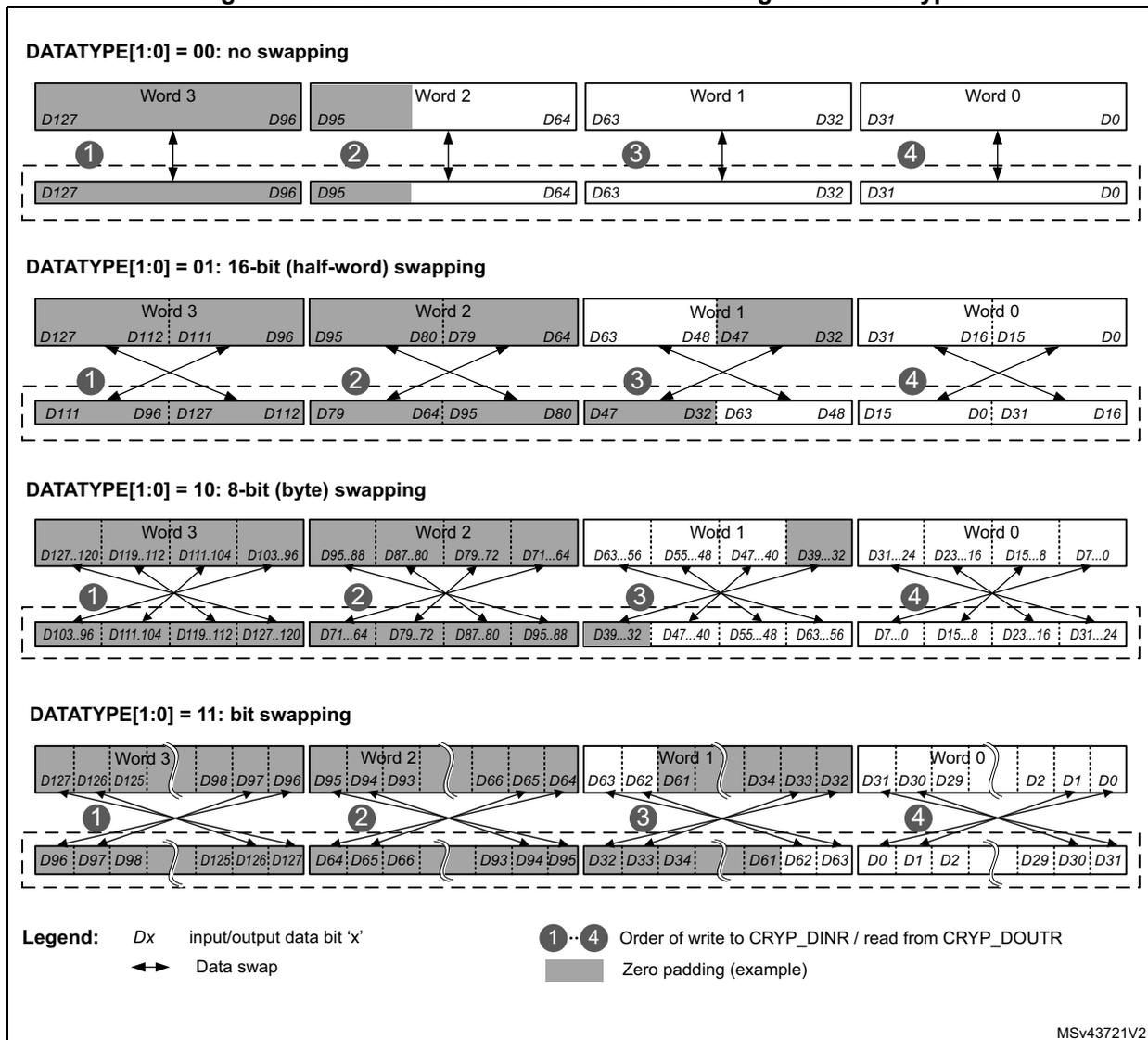
DATATYPE[1:0] = 00: no swapping
Word 3 (D127..D96), Word 2 (D95..D64), Word 1 (D63..D32), Word 0 (D31..D0) are written/read in order. No internal swapping occurs.
DATATYPE[1:0] = 01: 16-bit (half-word) swapping
Each 32-bit word is split into two 16-bit half-words which are swapped. For example, Word 3 (D127..D96) becomes D112..D96 followed by D127..D111.
DATATYPE[1:0] = 10: 8-bit (byte) swapping
Each 32-bit word is split into four 8-bit bytes which are byte-swapped. For example, Word 3 (D127..D96) becomes D103..D96 followed by D111..D104, then D119..D112, and finally D127..D120.
DATATYPE[1:0] = 11: bit swapping
Each 32-bit word is split into eight 4-bit nibbles which are bit-swapped. For example, Word 3 (D127..D96) becomes D125..D120 followed by D127..D122, then D119..D114, and finally D121..D116.
Legend:
- \( D_x \) input/output data bit 'x'
- 1...4 Order of write to CRYP_DINR / read from CRYP_DOUTR
- ↔ Data swap
- ▒ Zero padding (example)
MSV43721V2
20.4.17 CRYP key registers
The CRYP_Kx registers are write-only registers used to store the encryption or decryption keys. They are organized as four 64-bit registers, as shown in Table 148 and Table 149 .
Note: In memory and in CRYP key registers, AES and DES/TDES keys are stored in big-endian format, with most significant byte on the lowest address.
Table 148. Key endianness in CRYP_KxR/LR registers (AES 128/192/256-bit keys)
| K0LR[31:0] | K0RR[31:0] | K1LR[31:0] | K1RR[31:0] | K2LR[31:0] | K2RR[31:0] | K3LR[31:0] | K3RR[31:0] |
|---|---|---|---|---|---|---|---|
| - | - | - | - | k[127:96] | k[95:64] | k[63:32] | k[31:0] |
| K0LR[31:0] | K0RR[31:0] | K1LR[31:0] | K1RR[31:0] | K2LR[31:0] | K2RR[31:0] | K3LR[31:0] | K3RR[31:0] |
| - | - | k[191:160] | k[159:128] | k[127:96] | k[95:64] | k[63:32] | k[31:0] |
| K0LR[31:0] | K0RR[31:0] | K1LR[31:0] | K1RR[31:0] | K2LR[31:0] | K2RR[31:0] | K3LR[31:0] | K3RR[31:0] |
| k[255:224] | k[223:192] | k[191:160] | k[159:128] | k[127:96] | k[95:64] | k[63:32] | k[31:0] |
Table 149. Key endianness in CRYP_KxR/LR registers (DES K1 and TDES K1/2/3)
| K0LR[31:0] | K0RR[31:0] | K1LR[31:0] | K1RR[31:0] | K2LR[31:0] | K2RR[31:0] | K3LR[31:0] | K3RR[31:0] |
|---|---|---|---|---|---|---|---|
| - | - | K1[64:33] | K1[32:1] | - | - | - | - |
| - | - | K1[64:33] | K1[32:1] | K2[64:33] | K2[32:1] | K3[64:33] | K3[32:1] |
As shown on Table 149 , when TDES is selected (ALGOMODE[2:0] = 000 or 001) a 3-key vector (K1, K2, and K3) is used. When DES is selected (ALGOMODE[2:0] = 010 or 011) only 1-key vector (K1) is used.
Note: DES/TDES keys include 8-bit parity information that are not used by the cryptographic processor. In other words, bits 8, 16, 24, 32, 40, 48, 56 and 64 of each 64-bit key value Kx[1:64] are not used.
Write operations to the CRYP_Kx(L/R) registers when the BUSY bit is set to 1 in the CRYP_SR register are ignored (which means that the register content is not modified). The application must thus check that the BUSY bit is cleared to 0 before modifying key registers.
Key registers are not affected by the data swapping controlled by DATATYPE value in CRYP_CR register.
Refer to Section 20.7: CRYP registers for a detailed description of CRYP_Kx(L/R) registers.
20.4.18 CRYP initialization vector registers
The CRYP_IVxL/IVxR registers are used to store the initialization vector or the nonce, depending on the chaining mode selected. When used, these registers are updated by the core after each computation round of the TDES or AES core.
They are organized as four 64-bit registers, as shown in Table 150 and Table 151 . In DES/TDES mode only CRYP_IV0x are used.
Note: In memory and in CRYP IV registers, AES and DES/TDES initialization vectors are stored in big-endian format, with most significant byte on the lowest address.
Table 150. Initialization vector endianness in CRYP_IVx(L/R)R registers (AES)| CRYP_IV0LR[31:0] | CRYP_IV0RR[31:0] | CRYP_IV1LR[31:0] | CRYP_IV1RR[31:0] |
|---|---|---|---|
| IVI[127:96] | IVI[95:64] | IVI[63:32] | IVI[31:0] |
| CRYP_IV0LR[31:0] | CRYP_IV0RR[31:0] | CRYP_IV1LR[31:0] | CRYP_IV1RR[31:0] |
|---|---|---|---|
| IVI[64:32] | IVI[31:0] | - | - |
Any write operation to the CRYP_IV0...1(L/R)R registers when the BUSY bit is set to 1 in the CRYP_SR register is disregarded (which means that register content not modified). The software must thus check that the BUSY bit is cleared to 0 in the CRYP_SR register before modifying initialization vectors.
Reading the CRYP_IV0...1(L/R)R register returns the latest counter value (useful for managing suspend mode) except for CCM/GCM.
The initialization vector registers are not affected by the data swapping feature controlled by DATATYPE value in CRYP_CR register.
Refer to Section 20.7: CRYP registers for a detailed description of CRYP_IVxL/IVxR registers.
20.4.19 CRYP DMA interface
The cryptographic processor provides an interface to connect to the DMA (Direct Memory Access) controller. The DMA operation is controlled through the CRYP DMA control register (CRYP_DMACR).
Data input using DMA
DMA can be enabled for writing data into the cryptographic peripheral by setting the DIEN bit in the CRYP_DMACR register. When this bit is set, the cryptographic processor initiates a DMA request during the INPUT phase each time it requires a word to be written to the CRYP_DIN register.
Table 152 shows the recommended configuration to transfer data from memory to cryptographic processor through the DMA controller.
Table 152. Cryptographic processor configuration for memory-to-peripheral DMA transfers| DMA channel control register field | Programming recommendation |
|---|---|
| Transfer size | Message length, multiple of four 32-bit words. This 128-bit granularity corresponds to two blocks for DES/TDES, one block for AES. According to the algorithm and the mode selected, special padding/ciphertext stealing might be required. Refer to Section 20.4.8: CRYP stealing and data padding for details. |
| Source burst size (memory) | CRYP_FIFO_size /2 /transfer_width = 4 |
Table 152. Cryptographic processor configuration for memory-to-peripheral DMA transfers (continued)
| DMA channel control register field | Programming recommendation |
|---|---|
| Destination burst size (peripheral) | CRYP FIFO_size /2 /transfer_width = 4 (FIFO_size = 8x32-bit, transfer_width = 32-bit) |
| DMA FIFO size | CRYP FIFO_size /2 = 16 bytes |
| Source transfer width (memory) | 32-bit words |
| Destination transfer width (peripheral) | 32-bit words |
| Source address increment (memory) | Yes, after each 32-bit transfer. |
| Destination address increment (peripheral) | Fixed address of CRYP_DIN shall be used (no increment). |
Data output using DMA
To enable the DMA for reading data from CRYP processor, set the DOEN bit in the CRYP_DMACR register. When this bit is set, the cryptographic processor initiates a DMA request during the OUTPUT phase each time it requires a word to be read from the CRYP_DOUT register.
Table 153 shows the recommended configuration to transfer data from cryptographic processor to memory through the DMA controller.
Table 153. Cryptographic processor configuration for peripheral-to-memory DMA transfers
| DMA channel control register field | Programming recommendation |
|---|---|
| Transfer size | Message length, multiple of four 32-bit words. This 128-bit granularity corresponds to two blocks for DES/TDES, one block for AES. Depending on the chaining mode selected, extra bits have to be discarded. |
| Source burst size (peripheral) | When
DES
is used: Single transfer (burst size = 1) When AES is used: CRYP FIFO_size /2 /transfer_width = 4 (FIFO_size = 8x32-bit, transfer_width = 32-bit) |
| Destination burst size (memory) | CRYP FIFO_size /2 /transfer_width = 4 |
| DMA FIFO size | CRYP FIFO_size /2 = 16 bytes |
| Source transfer width (peripheral) | 32-bit words |
| memory transfer width (memory) | 32-bit words |
Table 153. Cryptographic processor configuration for peripheral-to-memory DMA transfers (continued)
| DMA channel control register field | Programming recommendation |
|---|---|
| Source address increment (peripheral) | Fixed address of CRYP_DOUT shall be used (no increment). |
| Destination address increment (memory) | Yes, after each 32-bit transfer. |
DMA mode
When AES is used, the cryptographic processor manages two DMA transfer requests through
cryp_in_dma
and
cryp_out_dma
internal input/output signals, which are asserted:
- • for IN FIFO: every time a block has been read from FIFO by CRYP,
- • for OUT FIFO: every time a block has been written into the FIFO by the cryptographic processor.
When DES/TDES is used, the cryptographic processor manages two DMA transfer requests through
cryp_in_dma
and
cryp_out_dma
internal input/output signals, which are asserted:
- • for IN FIFO: every time two blocks have been read from FIFO by the cryptographic processor
for OUT FIFO: every time a word has been written into the FIFO by the cryptographic processor (single transfer). Note that a burst transfer is also triggered when two blocks have been written into the FIFO.
All request signals are deasserted if the cryptographic peripheral is disabled or the DMA enable bit is cleared (DIEN bit for the IN FIFO and DOEN bit for the OUT FIFO in the CRYP_DMACR register).
Caution: It is important that DMA controller empties the cryptographic peripheral output FIFO before filling up the CRYP input FIFO. To achieve it, the DMA controller should be configured so that the transfer from the peripheral to the memory has a higher priority than the transfer from the memory to the peripheral.
For more detailed information on DMA operations, refer to Section 20.4.5: CRYP procedure to perform a cipher operation .
20.4.20 CRYP error management
No error flags are generated by the cryptographic processor.
20.5 CRYP interrupts
Overview
There are two individual maskable interrupt sources generated by the cryptographic processor to signal the following events:
- • Input FIFO empty or not full
- • Output FIFO full or not empty
These two sources are combined into a single interrupt signal which is the only interrupt signal from the CRYP processor that drives the Cortex® CPU interrupt controller. You can enable or disable CRYP interrupt sources individually by changing the mask bits in the CRYP_IMSCR register. Setting the appropriate mask bit to 1 enables the interrupt.
The status of the individual maskable interrupt sources can be read either from the CRYP_RISR register, for raw interrupt status, or from the CRYP_MISR register for masked interrupt status. The status of the individual source of event flags can be read from the CRYP_SR register.
Table 154 gives a summary of the available features.
Table 154. CRYP interrupt requests
| Interrupt acronym | Interrupt event | Event flag | Enable bit | Interrupt clear method | |
|---|---|---|---|---|---|
| in CRYP_xISR (1) | in CRYP_SR | ||||
| CRYP | Output FIFO full | OUTRIS (not masked) OUTMIS (masked) | OFFU | OUTIM
(2)
and CRYPEN | Read one data from output FIFO |
| Output FIFO not empty | OFNE | Read all data from output FIFO | |||
| Input FIFO not full | INRIS (not masked) INMIS (masked) | IFNF | INIM
(2)
and CRYPEN | Write data until input FIFO is full | |
| Input FIFO empty | IFEM | Write at least one word in input FIFO | |||
1. The flags belong to CRYP_RISR registers (unmasked or raw) or CRYP_MISR registers (masked).
2. The flags belong to CRYP_IMSCR register.
Output FIFO service interrupt - OUTMIS
The output FIFO service interrupt is asserted when there is one or more (32-bit word) data items in the output FIFO. This interrupt is cleared by reading data from the output FIFO until there is no valid (32-bit) word left (that is when the interrupt follows the state of the output FIFO not empty flag OFNE).
The output FIFO service interrupt OUTMIS is NOT enabled with the CRYP processor enable bit. Consequently, disabling the CRYP processor does not force the OUTMIS signal low if the output FIFO is not empty.
Input FIFO service interrupt - INMIS
The input FIFO service interrupt is asserted when there are less than four words in the input FIFO. It is cleared by performing write operations to the input FIFO until it holds four or more words.
The input FIFO service interrupt INMIS is enabled with the CRYP enable bit. Consequently, when CRYP is disabled, the INMIS signal is low even if the input FIFO is empty.
20.6 CRYP processing time
The time required to process a block for each mode of operation is summarized below. The block size is 128 bits for AES and 64 bits for DES/TDES.
Table 155. Processing latency for ECB, CBC and CTR
| Key size | Operating modes | Chaining algorithm | Clock cycles |
|---|---|---|---|
| 64 bits | DES encryption or decryption | ECD, CBC | 16 |
| 3x64 bits | TDES encryption or decryption | 48 | |
| 128 bits | AES encryption or decryption (1) | ECD, CBC, CTR | 14 |
| AES key preparation | - | 12 | |
| 192 bits | AES encryption or decryption (1) | ECD, CBC, CTR | 16 |
| AES key preparation | - | 14 | |
| 256 bits | AES encryption or decryption (1) | ECD, CBC, CTR | 18 |
| AES key preparation | - | 16 |
1. Excluding key preparation time (ECB and CBC only).
Table 156. Processing time (in clock cycle) for GCM and CCM per 128-bit block
| Key size | Operating modes | Chaining algorithm | Initialization phase | Header phase | Payload phase | Tag phase |
|---|---|---|---|---|---|---|
| 128 bits | AES encryption or decryption | GCM | 24 | 10 | 14 | 14 |
| CCM | 12 | 14 | 25 | 14 | ||
| 192 bits | GCM | 28 | 10 | 16 | 16 | |
| CCM | 14 | 16 | 29 | 16 | ||
| 256 bits | GCM | 32 | 10 | 18 | 18 | |
| CCM | 16 | 18 | 33 | 18 | ||
20.7 CRYP registers
The cryptographic core is associated with several control and status registers, eight key registers and four initialization vectors registers.
20.7.1 CRYP control register (CRYP_CR)
Address offset: 0x00
Reset value: 0x0000 0000
| 31 | 30 | 29 | 28 | 27 | 26 | 25 | 24 | 23 | 22 | 21 | 20 | 19 | 18 | 17 | 16 |
|---|---|---|---|---|---|---|---|---|---|---|---|---|---|---|---|
| Res. | Res. | Res. | Res. | Res. | Res. | Res. | Res. | Res. | ALGOMODE3 | Res. | GCM_CCMPH [1:0] | ||||
| rw | rw | rw | |||||||||||||
| 15 | 14 | 13 | 12 | 11 | 10 | 9 | 8 | 7 | 6 | 5 | 4 | 3 | 2 | 1 | 0 |
|---|---|---|---|---|---|---|---|---|---|---|---|---|---|---|---|
| CRYPEN | FFLUSH | Res. | Res. | Res. | Res. | KEYSIZE[1:0] | DATATYPE[1:0] | ALGOMODE[2:0] | ALGODIR | Res. | Res. | ||||
| rw | rw | rw | rw | rw | rw | rw | rw | rw | rw | ||||||
Bits 31:24 Reserved, must be kept at reset value.
Bits 23:20 Reserved, must be kept at reset value.
Bit 18 Reserved, must be kept at reset value.
Bits 17:16 GCM_CCMPH[1:0] : GCM or CCM Phase selection
This bitfield has no effect if GCM, GMAC or CCM algorithm is not selected in ALGOMODE field.
00: Initialization phase
01: Header phase
10: Payload phase
11: Final phase
Writing to GCM_CCMPH bits while BUSY = 1 has no effect.
Bit 15 CRYPEN : CRYP processor Enable
0: Cryptographic processor peripheral is disabled
1: Cryptographic processor peripheral is enabled
This bit is automatically cleared by hardware when the key preparation process ends (ALGOMODE = 0111) or after GCM/GMAC or CCM Initialization phase.
Bit 14 FFLUSH : CRYP FIFO Flush
0: No FIFO flush
1: FIFO flush enabled
When CRYPEN = 0, writing this bit to 1 flushes the IN and OUT FIFOs (that is read and write pointers of the FIFOs are reset). Writing this bit to 0 has no effect. When CRYPEN = 1, writing this bit to 0 or 1 has no effect.
Reading this bit always returns 0.
FFLUSH bit has to be set only when BUSY = 0. If not, the FIFO is flushed, but the block being processed may be pushed into the output FIFO just after the flush operation, resulting in a non-empty FIFO condition.
Bits 13:10 Reserved, must be kept at reset value.
Bits 9:8 KEYSIZE[1:0] : Key size selection (AES mode only)
This bitfield defines the bit-length of the key used for the AES cryptographic core. This bitfield is 'don't care' in the DES or TDES modes.
00: 128-bit key length
01: 192-bit key length
10: 256-bit key length
11: Reserved, do not use this value
Writing KEYSIZE bits while BUSY = 1 has no effect.
Bits 7:6 DATATYPE[1:0] : Data Type selection
This bitfield defines the format of data written in CRYP_DIN or read from CRYP_DOUT registers. For more details refer to Section 20.4.16: CRYP data registers and data swapping .
00: 32-bit data. No swapping for each word. First word pushed into the IN FIFO (or popped off the OUT FIFO) forms bits 1...32 of the data block, the second word forms bits 33...64 etc.
01: 16-bit data, or half-word. Each word pushed into the IN FIFO (or popped off the OUT FIFO) is considered as 2 half-words, which are swapped with each other.
10: 8-bit data, or bytes. Each word pushed into the IN FIFO (or popped off the OUT FIFO) is considered as 4 bytes, which are swapped with each other.
11: bit data, or bit-string. Each word pushed into the IN FIFO (or popped off the OUT FIFO) is considered as 32 bits (1st bit of the string at position 0), which are swapped with each other.
Writing DATATYPE bits while BUSY = 1 has no effect.
Bits 19, 5:3 ALGOMODE[3:0] : Algorithm mode
Below definition includes the bit 19:
0000: TDES-ECB (triple-DES Electronic Codebook).
0001: TDES-CBC (triple-DES Cipher Block Chaining).
0010: DES-ECB (simple DES Electronic Codebook).
0011: DES-CBC (simple DES Cipher Block Chaining).
0100: AES-ECB (AES Electronic Codebook).
0101: AES-CBC (AES Cipher Block Chaining).
0110: AES-CTR (AES Counter mode).
0111: AES key preparation for ECB or CBC decryption.
1000: AES-GCM (Galois Counter mode) and AES-GMAC (Galois Message Authentication Code mode).
1001: AES-CCM (Counter with CBC-MAC).
Writing ALGOMODE bits while BUSY = 1 has no effect.
Others: Reserved, must no be used
Bit 2 ALGODIR : Algorithm Direction
0: Encrypt
1: Decrypt
Writing ALGODIR bit while BUSY = 1 has no effect.
Bits 1:0 Reserved, must be kept at reset value.
20.7.2 CRYP status register (CRYP_SR)
Address offset: 0x04
Reset value: 0x0000 0003
| 31 | 30 | 29 | 28 | 27 | 26 | 25 | 24 | 23 | 22 | 21 | 20 | 19 | 18 | 17 | 16 |
|---|---|---|---|---|---|---|---|---|---|---|---|---|---|---|---|
| Res. | Res. | Res. | Res. | Res. | Res. | Res. | Res. | Res. | Res. | Res. | Res. | Res. | Res. | Res. | Res. |
| 15 | 14 | 13 | 12 | 11 | 10 | 9 | 8 | 7 | 6 | 5 | 4 | 3 | 2 | 1 | 0 |
| Res. | Res. | Res. | Res. | Res. | Res. | Res. | Res. | Res. | Res. | Res. | BUSY | OFFU | OFNE | IFNF | IFEM |
| r | r | r | r | r |
Bits 31:5 Reserved, must be kept at reset value.
Bit 4 BUSY : Busy bit
0: The CRYP core is not processing any data. The reason is:
- – either that the CRYP core is disabled (CRYPEN = 0 in the CRYP_CR register) and the last processing has completed,
- – or the CRYP core is waiting for enough data in the input FIFO or enough free space in the output FIFO (that is in each case at least 2 words in the DES, 4 words in the AES).
1: The CRYP core is currently processing a block of data or a key preparation is ongoing (AES ECB or CBC decryption only).
Bit 3 OFFU : Output FIFO full flag
0: Output FIFO is not full
1: Output FIFO is full
Bit 2 OFNE : Output FIFO not empty flag
0: Output FIFO is empty
1: Output FIFO is not empty
Bit 1 IFNF : Input FIFO not full flag
0: Input FIFO is full
1: Input FIFO is not full
Bit 0 IFEM : Input FIFO empty flag
0: Input FIFO is not empty
1: Input FIFO is empty
20.7.3 CRYP data input register (CRYP_DIN)
Address offset: 0x08
Reset value: 0x0000 0000
The CRYP_DIN register is the data input register. It is 32-bit wide. It is used to enter into the input FIFO up to four 64-bit blocks (TDES) or two 128-bit blocks (AES) of plaintext (when encrypting) or ciphertext (when decrypting), one 32-bit word at a time.
To fit different data sizes, the data can be swapped after processing by configuring the DATATYPE bits in the CRYP_CR register. Refer to Section 20.4.16: CRYP data registers and data swapping for more details.
When CRYP_DIN register is written to the data are pushed into the input FIFO.
- • If CRYPTEN = 1, when at least four 32-bit words in the AES mode have been pushed into the input FIFO (two words in the DES/TDES mode), and when at least four words are free in the output FIFO (two words in the DES/TDES mode), the CRYP engine starts an encrypting or decrypting process.
When CRYP_DIN register is read:
- • If CRYPTEN = 0, the FIFO is popped, and then the data present in the Input FIFO are returned, from the oldest one (first reading) to the newest one (last reading). The IFEM flag must be checked before each read operation to make sure that the FIFO is not empty.
- • if CRYPTEN = 1, an undefined value is returned.
Note: After the CRYP_DIN register has been read once or several times, the FIFO must be flushed by setting the FFLUSH bit prior to processing new data.
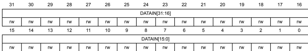
| 31 | 30 | 29 | 28 | 27 | 26 | 25 | 24 | 23 | 22 | 21 | 20 | 19 | 18 | 17 | 16 |
| DATAIN[31:16] | |||||||||||||||
| rw | rw | rw | rw | rw | rw | rw | rw | rw | rw | rw | rw | rw | rw | rw | rw |
| 15 | 14 | 13 | 12 | 11 | 10 | 9 | 8 | 7 | 6 | 5 | 4 | 3 | 2 | 1 | 0 |
| DATAIN[15:0] | |||||||||||||||
| rw | rw | rw | rw | rw | rw | rw | rw | rw | rw | rw | rw | rw | rw | rw | rw |
Bits 31:0 DATAIN[31:0] : Data input
On read FIFO is popped (last written value is returned), and its value is returned if CRYPTEN = 0. If CRYPTEN = 1 DATAIN register returns an undefined value.
On write current register content is pushed inside the FIFO.
20.7.4 CRYP data output register (CRYP_DOUT)
Address offset: 0x0C
Reset value: 0x0000 0000
The CRYP_DOUT register is the data output register. It is read-only and 32-bit wide. It is used to retrieve from the output FIFO up to four 64-bit blocks (TDES) or two 128-bit blocks
(AES) of plaintext (when encrypting) or ciphertext (when decrypting), one 32-bit word at a time.
To fit different data sizes, the data can be swapped after processing by configuring the DATATYPE bits in the CRYP_CR register. Refer to Section 20.4.16: CRYP data registers and data swapping for more details.
When CRYP_DOUT register is read, the last data entered into the output FIFO (pointed to by the read pointer) is returned.

| 31 | 30 | 29 | 28 | 27 | 26 | 25 | 24 | 23 | 22 | 21 | 20 | 19 | 18 | 17 | 16 |
| DATAOUT[31:16] | |||||||||||||||
| r | r | r | r | r | r | r | r | r | r | r | r | r | r | r | r |
| 15 | 14 | 13 | 12 | 11 | 10 | 9 | 8 | 7 | 6 | 5 | 4 | 3 | 2 | 1 | 0 |
| DATAOUT[15:0] | |||||||||||||||
| r | r | r | r | r | r | r | r | r | r | r | r | r | r | r | r |
Bits 31:0 DATAOUT[31:0] : Data output
On read returns output FIFO content (pointed to by read pointer), else returns an undefined value.
On write, no effect.
20.7.5 CRYP DMA control register (CRYP_DMACR)
Address offset: 0x10
Reset value: 0x0000 0000
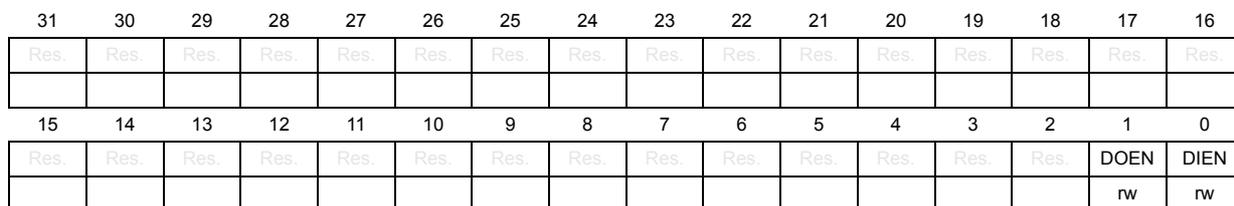
| 31 | 30 | 29 | 28 | 27 | 26 | 25 | 24 | 23 | 22 | 21 | 20 | 19 | 18 | 17 | 16 |
| Res. | Res. | Res. | Res. | Res. | Res. | Res. | Res. | Res. | Res. | Res. | Res. | Res. | Res. | Res. | Res. |
| 15 | 14 | 13 | 12 | 11 | 10 | 9 | 8 | 7 | 6 | 5 | 4 | 3 | 2 | 1 | 0 |
| Res. | Res. | Res. | Res. | Res. | Res. | Res. | Res. | Res. | Res. | Res. | Res. | Res. | Res. | DOEN | DIEN |
| rw | rw |
Bits 31:2 Reserved, must be kept at reset value.
Bit 1 DOEN : DMA output enable
When this bit is set, DMA requests are automatically generated by the peripheral during the output data phase.
0: Outgoing data transfer from CRYP via DMA is disabled
1: Outgoing data transfer from CRYP via DMA is enabled
Bit 0 DIEN : DMA input enable
When this bit is set, DMA requests are automatically generated by the peripheral during the input data phase.
0: Incoming data transfer to CRYP via DMA is disabled
1: Incoming data transfer to CRYP via DMA is enabled
20.7.6 CRYP interrupt mask set/clear register (CRYP_IMSCR)
Address offset: 0x14
Reset value: 0x0000 0000
The CRYP_IMSCR register is the interrupt mask set or clear register. It is a read/write register. When a read operation is performed, this register gives the current value of the mask applied to the relevant interrupt. Writing 1 to the particular bit sets the mask, thus enabling the interrupt to be read. Writing 0 to this bit clears the corresponding mask. All the bits are cleared to 0 when the peripheral is reset.
| 31 | 30 | 29 | 28 | 27 | 26 | 25 | 24 | 23 | 22 | 21 | 20 | 19 | 18 | 17 | 16 |
|---|---|---|---|---|---|---|---|---|---|---|---|---|---|---|---|
| Res. | Res. | Res. | Res. | Res. | Res. | Res. | Res. | Res. | Res. | Res. | Res. | Res. | Res. | Res. | Res. |
| 15 | 14 | 13 | 12 | 11 | 10 | 9 | 8 | 7 | 6 | 5 | 4 | 3 | 2 | 1 | 0 |
| Res. | Res. | Res. | Res. | Res. | Res. | Res. | Res. | Res. | Res. | Res. | Res. | Res. | Res. | OUTIM rw | INIM rw |
Bits 31:2 Reserved, must be kept at reset value.
Bit 1 OUTIM : Output FIFO service interrupt mask
0: Output FIFO service interrupt is masked
1: Output FIFO service interrupt is not masked
Bit 0 INIM : Input FIFO service interrupt mask
0: Input FIFO service interrupt is masked
1: Input FIFO service interrupt is not masked
20.7.7 CRYP raw interrupt status register (CRYP_RISR)
Address offset: 0x18
Reset value: 0x0000 0001
The CRYP_RISR register is the raw interrupt status register. It is a read-only register. When a read operation is performed, this register gives the current raw status of the corresponding interrupt, i.e. the interrupt information without taking CRYP_IMSCR mask into account. Write operations have no effect.
| 31 | 30 | 29 | 28 | 27 | 26 | 25 | 24 | 23 | 22 | 21 | 20 | 19 | 18 | 17 | 16 |
|---|---|---|---|---|---|---|---|---|---|---|---|---|---|---|---|
| Res. | Res. | Res. | Res. | Res. | Res. | Res. | Res. | Res. | Res. | Res. | Res. | Res. | Res. | Res. | Res. |
| 15 | 14 | 13 | 12 | 11 | 10 | 9 | 8 | 7 | 6 | 5 | 4 | 3 | 2 | 1 | 0 |
| Res. | Res. | Res. | Res. | Res. | Res. | Res. | Res. | Res. | Res. | Res. | Res. | Res. | Res. | OUTRIS r | INRIS r |
Bits 31:2 Reserved, must be kept at reset value.
Bit 1 OUTRIS : Output FIFO service raw interrupt status
This bit gives the output FIFO interrupt information without taking CRYP_IMSCR corresponding mask into account.
0: Raw interrupt not pending
1: Raw interrupt pending
Bit 0 INRIS : Input FIFO service raw interrupt status
This bit gives the input FIFO interrupt information without taking CRYP_IMSCR corresponding mask into account.
0: Raw interrupt not pending
1: Raw interrupt pending
20.7.8 CRYP masked interrupt status register (CRYP_MISR)
Address offset: 0x1C
Reset value: 0x0000 0000
The CRYP_MISR register is the masked interrupt status register. It is a read-only register. When a read operation is performed, this register gives the current masked status of the corresponding interrupt, i.e. the interrupt information taking CRYP_IMSCR mask into account. Write operations have no effect.
| 31 | 30 | 29 | 28 | 27 | 26 | 25 | 24 | 23 | 22 | 21 | 20 | 19 | 18 | 17 | 16 |
|---|---|---|---|---|---|---|---|---|---|---|---|---|---|---|---|
| Res. | Res. | Res. | Res. | Res. | Res. | Res. | Res. | Res. | Res. | Res. | Res. | Res. | Res. | Res. | Res. |
| 15 | 14 | 13 | 12 | 11 | 10 | 9 | 8 | 7 | 6 | 5 | 4 | 3 | 2 | 1 | 0 |
| Res. | Res. | Res. | Res. | Res. | Res. | Res. | Res. | Res. | Res. | Res. | Res. | Res. | Res. | OUTMIS | INMIS |
| r | r |
Bits 31:2 Reserved, must be kept at reset value.
Bit 1 OUTMIS : Output FIFO service masked interrupt status
This bit gives the output FIFO interrupt information taking into account the corresponding CRYP_IMSCR mask.
0: Output FIFO interrupt not pending
1: Output FIFO interrupt pending
Bit 0 INMIS : Input FIFO service masked interrupt status
This bit gives the input FIFO interrupt information taking into account the corresponding CRYP_IMSCR mask.
0: Input FIFO interrupt not pending
1: Input FIFO interrupt pending when CRYPTEN = 1
20.7.9 CRYP key register 0L (CRYP_K0LR)
Address offset: 0x20
Reset value: 0x0000 0000
CRYP key registers contain the cryptographic keys.
For more information refer to Section 20.4.17: CRYP key registers .
Note: Write accesses to these registers are disregarded when the cryptographic processor is busy (bit BUSY = 1 in the CRYP_SR register) .
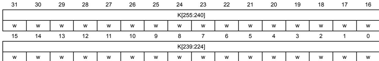
| 31 | 30 | 29 | 28 | 27 | 26 | 25 | 24 | 23 | 22 | 21 | 20 | 19 | 18 | 17 | 16 |
| K[255:240] | |||||||||||||||
| w | w | w | w | w | w | w | w | w | w | w | w | w | w | w | w |
| 15 | 14 | 13 | 12 | 11 | 10 | 9 | 8 | 7 | 6 | 5 | 4 | 3 | 2 | 1 | 0 |
| K[239:224] | |||||||||||||||
| w | w | w | w | w | w | w | w | w | w | w | w | w | w | w | w |
Bits 31:0 K[255:224] : Key bit x (x = 255 to 224)
This write-only bitfield contains the bits [255:224] of the AES encryption or decryption key, depending on the operating mode. This register is not used in DES/TDES mode.
20.7.10 CRYP key register 0R (CRYP_K0RR)
Address offset: 0x24
Reset value: 0x0000 0000
Refer to Section 20.7.9: CRYP key register 0L (CRYP_K0LR) for details.
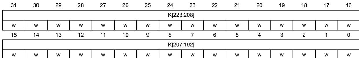
| 31 | 30 | 29 | 28 | 27 | 26 | 25 | 24 | 23 | 22 | 21 | 20 | 19 | 18 | 17 | 16 |
| K[223:208] | |||||||||||||||
| w | w | w | w | w | w | w | w | w | w | w | w | w | w | w | w |
| 15 | 14 | 13 | 12 | 11 | 10 | 9 | 8 | 7 | 6 | 5 | 4 | 3 | 2 | 1 | 0 |
| K[207:192] | |||||||||||||||
| w | w | w | w | w | w | w | w | w | w | w | w | w | w | w | w |
Bits 31:0 K[223:192] : Key bit x (x = 223 to 192)
This write-only bitfield contains the bits [223:192] of the AES encryption or decryption key, depending on the operating mode. This register is not used in DES/TDES mode.
20.7.11 CRYP key register 1L (CRYP_K1LR)
Address offset: 0x28
Reset value: 0x0000 0000
Refer to Section 20.7.9: CRYP key register 0L (CRYP_K0LR) for details.
| 31 | 30 | 29 | 28 | 27 | 26 | 25 | 24 | 23 | 22 | 21 | 20 | 19 | 18 | 17 | 16 |
| K[191:176] | |||||||||||||||
| w | w | w | w | w | w | w | w | w | w | w | w | w | w | w | w |
| 15 | 14 | 13 | 12 | 11 | 10 | 9 | 8 | 7 | 6 | 5 | 4 | 3 | 2 | 1 | 0 |
| K[175:160] | |||||||||||||||
| w | w | w | w | w | w | w | w | w | w | w | w | w | w | w | w |
Bits 31:0 K[191:160] : Key bit x (x = 191 to 160)
This write-only bitfield contains the bits [191:160] of the AES encryption or decryption key, depending on the operating mode. In DES/TDES mode this bitfield contains the bits [64:33] of the key K1, with parity bits unused.
20.7.12 CRYP key register 1R (CRYP_K1RR)
Address offset: 0x2C
Reset value: 0x0000 0000
Refer to Section 20.7.9: CRYP key register 0L (CRYP_K0LR) for details.
| 31 | 30 | 29 | 28 | 27 | 26 | 25 | 24 | 23 | 22 | 21 | 20 | 19 | 18 | 17 | 16 |
| K[159:144] | |||||||||||||||
| w | w | w | w | w | w | w | w | w | w | w | w | w | w | w | w |
| 15 | 14 | 13 | 12 | 11 | 10 | 9 | 8 | 7 | 6 | 5 | 4 | 3 | 2 | 1 | 0 |
| K[143:128] | |||||||||||||||
| w | w | w | w | w | w | w | w | w | w | w | w | w | w | w | w |
Bits 31:0 K[159:128] : Key bit x (x = 159 to 128)
This write-only bitfield contains the bits [159:128] of the AES encryption or decryption key, depending on the operating mode. In DES/TDES mode this bitfield contains the bits [32:1] of the key K1, with parity bits unused.
20.7.13 CRYP key register 2L (CRYP_K2LR)
Address offset: 0x30
Reset value: 0x0000 0000
Refer to Section 20.7.9: CRYP key register 0L (CRYP_K0LR) for details.
| 31 | 30 | 29 | 28 | 27 | 26 | 25 | 24 | 23 | 22 | 21 | 20 | 19 | 18 | 17 | 16 |
| K[127:112] | |||||||||||||||
| w | w | w | w | w | w | w | w | w | w | w | w | w | w | w | w |
| 15 | 14 | 13 | 12 | 11 | 10 | 9 | 8 | 7 | 6 | 5 | 4 | 3 | 2 | 1 | 0 |
| K[111:96] | |||||||||||||||
| w | w | w | w | w | w | w | w | w | w | w | w | w | w | w | w |
Bits 31:0 K[127:96] : Key bit x (x = 127 to 96)
This write-only bitfield contains the bits [127:96] of the AES encryption or decryption key, depending on the operating mode. In DES/TDES mode this bitfield contains the bits [64:33] of the key K2, with parity bits unused.
20.7.14 CRYP key register 2R (CRYP_K2RR)
Address offset: 0x34
Reset value: 0x0000 0000
Refer to Section 20.7.9: CRYP key register 0L (CRYP_K0LR) for details.
| 31 | 30 | 29 | 28 | 27 | 26 | 25 | 24 | 23 | 22 | 21 | 20 | 19 | 18 | 17 | 16 |
| K[95:80] | |||||||||||||||
| w | w | w | w | w | w | w | w | w | w | w | w | w | w | w | w |
| 15 | 14 | 13 | 12 | 11 | 10 | 9 | 8 | 7 | 6 | 5 | 4 | 3 | 2 | 1 | 0 |
| K[79:64] | |||||||||||||||
| w | w | w | w | w | w | w | w | w | w | w | w | w | w | w | w |
Bits 31:0 K[95:64] : Key bit x (x = 95 to 64)
This write-only bitfield contains the bits [95:64] of the AES encryption or decryption key, depending on the operating mode. In DES/TDES mode this bitfield contains the bits [32:1] of the key K2, with parity bits unused.
20.7.15 CRYP key register 3L (CRYP_K3LR)
Address offset: 0x38
Reset value: 0x0000 0000
Refer to Section 20.7.9: CRYP key register 0L (CRYP_K0LR) for details.
| 31 | 30 | 29 | 28 | 27 | 26 | 25 | 24 | 23 | 22 | 21 | 20 | 19 | 18 | 17 | 16 |
| K[63:48] | |||||||||||||||
| w | w | w | w | w | w | w | w | w | w | w | w | w | w | w | w |
| 15 | 14 | 13 | 12 | 11 | 10 | 9 | 8 | 7 | 6 | 5 | 4 | 3 | 2 | 1 | 0 |
| K[47:32] | |||||||||||||||
| w | w | w | w | w | w | w | w | w | w | w | w | w | w | w | w |
Bits 31:0 K[63:32] : Key bit x (x = 63 to 32)
This write-only bitfield contains the bits [63:32] of the AES encryption or decryption key, depending on the operating mode. In DES/TDES mode this bitfield contains the bits [64:33] of the key K3, with parity bits unused.
20.7.16 CRYP key register 3R (CRYP_K3RR)
Address offset: 0x3C
Reset value: 0x0000 0000
Refer to Section 20.7.9: CRYP key register 0L (CRYP_K0LR) for details.
| 31 | 30 | 29 | 28 | 27 | 26 | 25 | 24 | 23 | 22 | 21 | 20 | 19 | 18 | 17 | 16 |
| K[31:16] | |||||||||||||||
| w | w | w | w | w | w | w | w | w | w | w | w | w | w | w | w |
| 15 | 14 | 13 | 12 | 11 | 10 | 9 | 8 | 7 | 6 | 5 | 4 | 3 | 2 | 1 | 0 |
| K[15:0] | |||||||||||||||
| w | w | w | w | w | w | w | w | w | w | w | w | w | w | w | w |
Bits 31:0 K[31:0] : Key bit x (x = 31 to 0)
This write-only bitfield contains the bits [31:0] of the AES encryption or decryption key, depending on the operating mode. In DES/TDES mode this bitfield contains the bits [32:1] of the key K3, with parity bits unused.
20.7.17 CRYP initialization vector register 0L (CRYP_IV0LR)
Address offset: 0x40
Reset value: 0x0000 0000
The CRYP_IVx(L/R)R registers store the initialization vector or the nonce, depending on the chaining mode selected. The size of the IV data is 64 bits for DES/TDES and 128 bits for AES. For more information refer to Section 20.4.18: CRYP initialization vector registers .
Note: Write accesses to these registers are disregarded when the cryptographic processor is busy (BUSY = 1 in the CRYP_SR register).
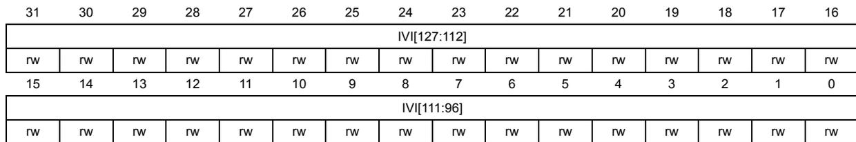
| 31 | 30 | 29 | 28 | 27 | 26 | 25 | 24 | 23 | 22 | 21 | 20 | 19 | 18 | 17 | 16 |
| IVI[127:112] | |||||||||||||||
| rw | rw | rw | rw | rw | rw | rw | rw | rw | rw | rw | rw | rw | rw | rw | rw |
| 15 | 14 | 13 | 12 | 11 | 10 | 9 | 8 | 7 | 6 | 5 | 4 | 3 | 2 | 1 | 0 |
| IVI[111:96] | |||||||||||||||
| rw | rw | rw | rw | rw | rw | rw | rw | rw | rw | rw | rw | rw | rw | rw | rw |
Bits 31:0 IVI[127:96] : Initialization vector bit x (x = 127 to 96)
This bitfield stores the initialization vector bits [127:96] for AES chaining modes other than ECB. In DES/TDES mode it corresponds to IVI bits [63:32].
IV registers are updated by the core after each computation round of the DES/TDES or AES core.
20.7.18 CRYP initialization vector register 0R (CRYP_IV0RR)
Address offset: 0x44
Reset value: 0x0000 0000
Refer to Section 20.7.17: CRYP initialization vector register 0L (CRYP_IV0LR) for details.
| 31 | 30 | 29 | 28 | 27 | 26 | 25 | 24 | 23 | 22 | 21 | 20 | 19 | 18 | 17 | 16 |
| IVI[95:80] | |||||||||||||||
| rw | rw | rw | rw | rw | rw | rw | rw | rw | rw | rw | rw | rw | rw | rw | rw |
| 15 | 14 | 13 | 12 | 11 | 10 | 9 | 8 | 7 | 6 | 5 | 4 | 3 | 2 | 1 | 0 |
| IVI[79:64] | |||||||||||||||
| rw | rw | rw | rw | rw | rw | rw | rw | rw | rw | rw | rw | rw | rw | rw | rw |
Bits 31:0 IVI[95:64] : Initialization vector bit x (x = 95 to 64)
This bitfield stores the initialization vector bits [95:64] for AES chaining modes other than ECB. In DES/TDES mode it corresponds to IVI bits [31:0].
IV registers are updated by the core after each computation round of the DES/TDES or AES core.
20.7.19 CRYP initialization vector register 1L (CRYP_IV1LR)
Address offset: 0x48
Reset value: 0x0000 0000
Refer to Section 20.7.17: CRYP initialization vector register 0L (CRYP_IV0LR) for details.
| 31 | 30 | 29 | 28 | 27 | 26 | 25 | 24 | 23 | 22 | 21 | 20 | 19 | 18 | 17 | 16 |
| IVI[63:48] | |||||||||||||||
| rw | rw | rw | rw | rw | rw | rw | rw | rw | rw | rw | rw | rw | rw | rw | rw |
| 15 | 14 | 13 | 12 | 11 | 10 | 9 | 8 | 7 | 6 | 5 | 4 | 3 | 2 | 1 | 0 |
| IVI[47:32] | |||||||||||||||
| rw | rw | rw | rw | rw | rw | rw | rw | rw | rw | rw | rw | rw | rw | rw | rw |
Bits 31:0 IVI[63:32] : Initialization vector bit x (x = 63 to 32)
This bitfield stores the initialization vector bits [63:32] for AES chaining modes other than ECB. This register is not used in DES mode.
IV registers are updated by the core after each computation round of the AES core.
20.7.20 CRYP initialization vector register 1R (CRYP_IV1RR)
Address offset: 0x4C
Reset value: 0x0000 0000
Refer to Section 20.7.17: CRYP initialization vector register 0L (CRYP_IV0LR) for details.
| 31 | 30 | 29 | 28 | 27 | 26 | 25 | 24 | 23 | 22 | 21 | 20 | 19 | 18 | 17 | 16 |
| IVI[31:16] | |||||||||||||||
| rw | rw | rw | rw | rw | rw | rw | rw | rw | rw | rw | rw | rw | rw | rw | rw |
| 15 | 14 | 13 | 12 | 11 | 10 | 9 | 8 | 7 | 6 | 5 | 4 | 3 | 2 | 1 | 0 |
| IVI[15:0] | |||||||||||||||
| rw | rw | rw | rw | rw | rw | rw | rw | rw | rw | rw | rw | rw | rw | rw | rw |
Bits 31:0 IVI[31:0] : Initialization vector bit x (x = 31 to 0)
This bitfield stores the initialization vector bits [31:0] for AES chaining modes other than ECB. This register is not used in DES mode.
IV registers are updated by the core after each computation round of the AES core.
20.7.21 CRYP register map
Table 157. CRYP register map and reset values
| Offset | Register name reset value | 31 | 30 | 29 | 28 | 27 | 26 | 25 | 24 | 23 | 22 | 21 | 20 | 19 | 18 | 17 | 16 | 15 | 14 | 13 | 12 | 11 | 10 | 9 | 8 | 7 | 6 | 5 | 4 | 3 | 2 | 1 | 0 |
|---|---|---|---|---|---|---|---|---|---|---|---|---|---|---|---|---|---|---|---|---|---|---|---|---|---|---|---|---|---|---|---|---|---|
| 0x00 | CRYP_CR | Res. | Res. | Res. | Res. | Res. | Res. | Res. | Res. | Res. | ALGOMODE[3] | Res. | GCM_CCMPH | CRYPEN | FFLUSH | Res. | Res. | Res. | Res. | KEYSIZE | DATATYPE | ALGOMODE[2:0] | ALGODIR | Res. | Res. | ||||||||
| Reset value | 0 | 0 | 0 | 0 | 0 | 0 | 0 | 0 | 0 | 0 | 0 | 0 | 0 | 0 | 0 | 0 | 0 | ||||||||||||||||
Table 157. CRYP register map and reset values (continued)
| Offset | Register name reset value | 31 | 30 | 29 | 28 | 27 | 26 | 25 | 24 | 23 | 22 | 21 | 20 | 19 | 18 | 17 | 16 | 15 | 14 | 13 | 12 | 11 | 10 | 9 | 8 | 7 | 6 | 5 | 4 | 3 | 2 | 1 | 0 | |
|---|---|---|---|---|---|---|---|---|---|---|---|---|---|---|---|---|---|---|---|---|---|---|---|---|---|---|---|---|---|---|---|---|---|---|
| 0x04 | CRYP_SR | Res | Res | Res | Res | Res | Res | Res | Res | Res | Res | Res | Res | Res | Res | Res | Res | Res | Res | Res | Res | Res | Res | Res | Res | Res | Res | Res | Res | BUSY | OFFU | OFNE | IFNF | IFEM |
| Reset value | 0 | 0 | 0 | 1 | 1 | |||||||||||||||||||||||||||||
| 0x08 | CRYP_DIN | DATAIN | ||||||||||||||||||||||||||||||||
| Reset value | 0 | 0 | 0 | 0 | 0 | 0 | 0 | 0 | 0 | 0 | 0 | 0 | 0 | 0 | 0 | 0 | 0 | 0 | 0 | 0 | 0 | 0 | 0 | 0 | 0 | 0 | 0 | 0 | 0 | 0 | 0 | 0 | 0 | |
| 0x0C | CRYP_DOUT | DATAOUT | ||||||||||||||||||||||||||||||||
| Reset value | 0 | 0 | 0 | 0 | 0 | 0 | 0 | 0 | 0 | 0 | 0 | 0 | 0 | 0 | 0 | 0 | 0 | 0 | 0 | 0 | 0 | 0 | 0 | 0 | 0 | 0 | 0 | 0 | 0 | 0 | 0 | 0 | 0 | |
| 0x10 | CRYP_DMACR | Res | Res | Res | Res | Res | Res | Res | Res | Res | Res | Res | Res | Res | Res | Res | Res | Res | Res | Res | Res | Res | Res | Res | Res | Res | Res | Res | Res | Res | Res | Res | DOEN | DIEN |
| Reset value | 0 | 0 | ||||||||||||||||||||||||||||||||
| 0x14 | CRYP_IMSCR | Res | Res | Res | Res | Res | Res | Res | Res | Res | Res | Res | Res | Res | Res | Res | Res | Res | Res | Res | Res | Res | Res | Res | Res | Res | Res | Res | Res | Res | Res | Res | OUTIM | INIM |
| Reset value | 0 | 0 | ||||||||||||||||||||||||||||||||
| 0x18 | CRYP_RISR | Res | Res | Res | Res | Res | Res | Res | Res | Res | Res | Res | Res | Res | Res | Res | Res | Res | Res | Res | Res | Res | Res | Res | Res | Res | Res | Res | Res | Res | Res | Res | OUTRIS | INRIS |
| Reset value | 0 | 1 | ||||||||||||||||||||||||||||||||
| 0x1C | CRYP_MISR | Res | Res | Res | Res | Res | Res | Res | Res | Res | Res | Res | Res | Res | Res | Res | Res | Res | Res | Res | Res | Res | Res | Res | Res | Res | Res | Res | Res | Res | Res | Res | OUTMIS | INMIS |
| Reset value | 0 | 0 | ||||||||||||||||||||||||||||||||
| 0x20 | CRYP_K0LR | K[255:224] | ||||||||||||||||||||||||||||||||
| Reset value | 0 | 0 | 0 | 0 | 0 | 0 | 0 | 0 | 0 | 0 | 0 | 0 | 0 | 0 | 0 | 0 | 0 | 0 | 0 | 0 | 0 | 0 | 0 | 0 | 0 | 0 | 0 | 0 | 0 | 0 | 0 | 0 | 0 | |
| 0x24 | CRYP_K0RR | K[223:192] | ||||||||||||||||||||||||||||||||
| Reset value | 0 | 0 | 0 | 0 | 0 | 0 | 0 | 0 | 0 | 0 | 0 | 0 | 0 | 0 | 0 | 0 | 0 | 0 | 0 | 0 | 0 | 0 | 0 | 0 | 0 | 0 | 0 | 0 | 0 | 0 | 0 | 0 | 0 | |
| ... | ||||||||||||||||||||||||||||||||||
| 0x38 | CRYP_K3LR | K[63:32] | ||||||||||||||||||||||||||||||||
| Reset value | 0 | 0 | 0 | 0 | 0 | 0 | 0 | 0 | 0 | 0 | 0 | 0 | 0 | 0 | 0 | 0 | 0 | 0 | 0 | 0 | 0 | 0 | 0 | 0 | 0 | 0 | 0 | 0 | 0 | 0 | 0 | 0 | 0 | |
| 0x3C | CRYP_K3RR | K[31:0] | ||||||||||||||||||||||||||||||||
| Reset value | 0 | 0 | 0 | 0 | 0 | 0 | 0 | 0 | 0 | 0 | 0 | 0 | 0 | 0 | 0 | 0 | 0 | 0 | 0 | 0 | 0 | 0 | 0 | 0 | 0 | 0 | 0 | 0 | 0 | 0 | 0 | 0 | 0 | |
| 0x40 | CRYP_IV0LR | IV[127:96] | ||||||||||||||||||||||||||||||||
| Reset value | 0 | 0 | 0 | 0 | 0 | 0 | 0 | 0 | 0 | 0 | 0 | 0 | 0 | 0 | 0 | 0 | 0 | 0 | 0 | 0 | 0 | 0 | 0 | 0 | 0 | 0 | 0 | 0 | 0 | 0 | 0 | 0 | 0 | |
| 0x44 | CRYP_IV0RR | IV[95:64] | ||||||||||||||||||||||||||||||||
| Reset value | 0 | 0 | 0 | 0 | 0 | 0 | 0 | 0 | 0 | 0 | 0 | 0 | 0 | 0 | 0 | 0 | 0 | 0 | 0 | 0 | 0 | 0 | 0 | 0 | 0 | 0 | 0 | 0 | 0 | 0 | 0 | 0 | 0 | |
| 0x48 | CRYP_IV1LR | IV[63:32] | ||||||||||||||||||||||||||||||||
| Reset value | 0 | 0 | 0 | 0 | 0 | 0 | 0 | 0 | 0 | 0 | 0 | 0 | 0 | 0 | 0 | 0 | 0 | 0 | 0 | 0 | 0 | 0 | 0 | 0 | 0 | 0 | 0 | 0 | 0 | 0 | 0 | 0 | 0 | |
| 0x4C | CRYP_IV1RR | IV[31:0] | ||||||||||||||||||||||||||||||||
| Reset value | 0 | 0 | 0 | 0 | 0 | 0 | 0 | 0 | 0 | 0 | 0 | 0 | 0 | 0 | 0 | 0 | 0 | 0 | 0 | 0 | 0 | 0 | 0 | 0 | 0 | 0 | 0 | 0 | 0 | 0 | 0 | 0 | 0 | |
Refer to Section 2.2 on page 66 for the register boundary addresses.