12. Flexible memory controller (FMC)
12.1 Introduction
The flexible memory controller (FMC) includes three memory controllers:
- • The NOR/PSRAM memory controller
- • The NAND memory controller
- • The Synchronous DRAM (SDRAM/Mobile LPSDR SDRAM) controller.
12.2 FMC main features
The FMC functional block makes the interface with: synchronous and asynchronous static memories, SDRAM memories, and NAND flash memory. Its main purposes are:
- • to translate AHB transactions into the appropriate external device protocol
- • to meet the access time requirements of the external memory devices
All external memories share the addresses, data and control signals with the controller. Each external device is accessed by means of a unique chip select. The FMC performs only one access at a time to an external device.
The main features of the FMC controller are the following:
- • Interface with static-memory mapped devices including:
- – Static random access memory (SRAM)
- – NOR flash memory/OneNAND flash memory
- – PSRAM (4 memory banks)
- – NAND flash memory with ECC hardware to check up to 8 Kbytes of data
- • Interface with synchronous DRAM (SDRAM/Mobile LPSDR SDRAM) memories
- • Interface with parallel LCD modules, supporting Intel 8080 and Motorola 6800 modes.
- • Burst mode support for faster access to synchronous devices such as NOR flash memory, PSRAM and SDRAM)
- • Programmable continuous clock output for asynchronous and synchronous accesses
- • 8-, 16- or 32-bit wide data bus
- • Independent chip select control for each memory bank
- • Independent configuration for each memory bank
- • Write enable and byte lane select outputs for use with PSRAM, SRAM and SDRAM devices
- • External asynchronous wait control
- • Write FIFO with 16 x32-bit depth
- • Cacheable Read FIFO with 6 x32-bit depth (6 x14-bit address tag) for SDRAM controller.
The Write FIFO is common to all memory controllers and consists of:
- • a Write Data FIFO which stores the AHB data to be written to the memory (up to 32 bits) plus one bit for the AHB transfer (burst or not sequential mode)
- • a Write Address FIFO which stores the AHB address (up to 28 bits) plus the AHB data size (up to 2 bits). When operating in burst mode, only the start address is stored
except when crossing a page boundary (for PSRAM and SDRAM). In this case, the AHB burst is broken into two FIFO entries.
The Write FIFO can be disabled by setting the WFDIS bit in the FMC_BCR1 register.
At startup the FMC pins must be configured by the user application. The FMC I/O pins which are not used by the application can be used for other purposes.
The FMC registers that define the external device type and associated characteristics are usually set at boot time and do not change until the next reset or power-up. However, the settings can be changed at any time.
12.3 FMC block diagram
The FMC consists of the following main blocks:
- • The AHB interface (including the FMC configuration registers)
- • The NOR flash/PSRAM/SRAM controller
- • The SDRAM controller
- • The external device interface
The block diagram is shown in the figure below.
Figure 36. FMC block diagram
The block diagram illustrates the internal architecture and external connections of the Flexible Memory Controller (FMC). The main components and their connections are as follows:
- Internal Components:
- Configuration registers: Connected to the AHB interface and the memory controllers.
- NOR/PSRAM memory controller: Manages NOR flash, PSRAM, and SRAM devices.
- NAND memory controller: Manages NAND flash devices.
- SDRAM controller: Manages SDRAM devices.
- External Connections:
- FMC interrupts to NVIC: An interrupt signal sent to the Nested Vectored Interrupt Controller.
- From clock controller HCLK: The system clock input.
- Signal Groups:
- NOR/PSRAM signals: FMC_NL (or NADV), FMC_CLK.
- NOR / PSRAM / SRAM shared signals: FMC_NBL[3:0].
- Shared signals: FMC_A[25:0] (address), FMC_D[31:0] (data).
- NOR / PSRAM / SRAM shared signals: FMC_NE[4:1], FMC_NOE, FMC_NWE, FMC_NWAIT.
- NAND signals: FMC_NCE, FMC_INT.
- SDRAM signals: FMC_SDCLK, FMC_SDNWE, FMC_SDCKE[1:0], FMC_SDNE[1:0], FMC_NRAS, FMC_NCAS.
MS30443V7
12.4 AHB interface
The AHB slave interface allows internal CPUs and other bus master peripherals to access the external memories.
AHB transactions are translated into the external device protocol. In particular, if the selected external memory is 16- or 8-bit wide, 32-bit wide transactions on the AHB are split into consecutive 16- or 8-bit accesses. The FMC chip select (FMC_NEx) does not toggle between the consecutive accesses except in case of Access mode D when the Extended mode is enabled.
The FMC generates an AHB error in the following conditions:
- • When reading or writing to a FMC bank (Bank 1 to 4) which is not enabled.
- • When reading or writing to the NOR flash bank while the FACCEN bit is reset in the FMC_BCRx register.
- • When writing to a write protected SDRAM bank (WP bit set in the SDRAM_SDCRx register).
- • When the SDRAM address range is violated (access to reserved address range)
The effect of an AHB error depends on the AHB master which has attempted the R/W access:
- • If the access has been attempted by the Cortex ® -M4 CPU, a hard fault interrupt is generated.
- • If the access has been performed by a DMA controller, a DMA transfer error is generated and the corresponding DMA channel is automatically disabled.
The AHB clock (HCLK) is the reference clock for the FMC.
12.4.1 Supported memories and transactions
General transaction rules
The requested AHB transaction data size can be 8-, 16- or 32-bit wide whereas the accessed external device has a fixed data width. This may lead to inconsistent transfers.
Therefore, some simple transaction rules must be followed:
- • AHB transaction size and memory data size are equal
There is no issue in this case.
- • AHB transaction size is greater than the memory size:
In this case, the FMC splits the AHB transaction into smaller consecutive memory accesses to meet the external data width. The FMC chip select (FMC_NEx) does not toggle between the consecutive accesses.
- • AHB transaction size is smaller than the memory size:
The transfer may or not be consistent depending on the type of external device:
- – Accesses to devices that have the byte select feature (SRAM, ROM, PSRAM, SDRAM)
In this case, the FMC allows read/write transactions and accesses to the right data through its byte lanes NBL[3:0].
Bytes to be written are addressed by NBL[3:0].
All memory bytes are read (NBL[3:0] are driven low during read transaction) and the useless ones are discarded.
- – Accesses to devices that do not have the byte select feature (NOR and NAND flash memories)
This situation occurs when a byte access is requested to a 16-bit wide flash memory. Since the device cannot be accessed in Byte mode (only 16-bit words can be read/written from/to the flash memory), Write transactions and Read transactions are allowed (the controller reads the entire 16-bit memory word and uses only the required byte).
Wrap support for NOR flash/PSRAM and SDRAM
Wrap burst mode for synchronous memories is not supported. The memories must be configured in Linear burst mode of undefined length.
Configuration registers
The FMC can be configured through a set of registers. Refer to Section 12.6.6 , for a detailed description of the NOR flash/PSRAM controller registers. Refer to Section 12.7.7 , for a detailed description of the NAND flash registers and to Section 12.8.5 for a detailed description of the SDRAM controller registers.
12.5 External device address mapping
From the FMC point of view, the external memory is divided into fixed-size banks of 256 Mbytes each (see Figure 37 ):
- • Bank 1 used to address up to 4 NOR flash memory or PSRAM devices. This bank is split into 4 NOR/PSRAM subbanks with 4 dedicated chip selects, as follows:
- – Bank 1 - NOR/PSRAM 1
- – Bank 1 - NOR/PSRAM 2
- – Bank 1 - NOR/PSRAM 3
- – Bank 1 - NOR/PSRAM 4
- • Bank 3 used to address NAND flash memory devices. The MPU memory attribute for this space must be reconfigured by software to Device.
- • Bank 4 and 5 used to address SDRAM devices (1 device per bank).
For each bank the type of memory to be used can be configured by the user application through the Configuration register.
Figure 37. FMC memory banks
| Address | Bank | Supported memory type |
|---|---|---|
| 0x6000 0000 | Bank 1 4 x 64 MB | NOR/PSRAM/ SRAM |
| 0x6FFF FFFF | ||
| 0x7000 0000 | Bank 2 Not used | |
| 0x7FFF FFFF | ||
| 0x8000 0000 | Bank 3 4 x 64 MB | NAND flash memory |
| 0x8FFF FFFF | ||
| 0x9000 0000 | Bank 4 Not used | |
| 0x9FFF FFFF | ||
| 0xC000 0000 | SDRAM Bank 1 4 x 64 MB | SDRAM |
| 0xCFFF FFFF | ||
| 0xD000 0000 | SDRAM Bank 2 4 x 64 MB | |
| 0xDFFF FFFF |
MSV69582V1
12.5.1 NOR/PSRAM address mapping
HADDR[27:26] bits are used to select one of the four memory banks as shown in Table 50 .
Table 50. NOR/PSRAM bank selection
| HADDR[27:26] (1) | Selected bank |
|---|---|
| 00 | Bank 1 - NOR/PSRAM 1 |
| 01 | Bank 1 - NOR/PSRAM 2 |
| 10 | Bank 1 - NOR/PSRAM 3 |
| 11 | Bank 1 - NOR/PSRAM 4 |
1. HADDR are internal AHB address lines that are translated to external memory.
The HADDR[25:0] bits contain the external memory address. Since HADDR is a byte address whereas the memory is addressed at word level, the address actually issued to the memory varies according to the memory data width, as shown in the following table.
Table 51. NOR/PSRAM External memory address| Memory width (1) | Data address issued to the memory | Maximum memory capacity (bits) |
|---|---|---|
| 8-bit | HADDR[25:0] | 64 Mbytes x 8 = 512 Mbits |
| 16-bit | HADDR[25:1] >> 1 | 64 Mbytes/2 x 16 = 512 Mbits |
| 32-bit | HADDR[25:2] >> 2 | 64 Mbytes/4 x 32 = 512 Mbits |
- 1. In case of a 16-bit external memory width, the FMC internally uses HADDR[25:1] to generate the address for external memory FMC_A[24:0]. In case of a 32-bit memory width, the FMC internally uses HADDR[25:2] to generate the external address.
Whatever the external memory width, FMC_A[0] must be connected to external memory address A[0].
12.5.2 NAND flash memory address mapping
The NAND bank is divided into memory areas as indicated in Table 52 .
Table 52. NAND memory mapping and timing registers| Start address | End address | FMC bank | Memory space | Timing register |
|---|---|---|---|---|
| 0x8800 0000 | 0x8BFF FFFF | Bank 3 - NAND flash | Attribute | FMC_PATT (0x8C) |
| 0x8000 0000 | 0x83FF FFFF | Common | FMC_PMEM (0x88) |
For NAND flash memory, the common and attribute memory spaces are subdivided into three sections (see in Table 53 below) located in the lower 256 Kbytes:
- • Data section (first 64 Kbytes in the common/attribute memory space)
- • Command section (second 64 Kbytes in the common / attribute memory space)
- • Address section (next 128 Kbytes in the common / attribute memory space)
| Section name | HADDR[17:16] | Address range |
|---|---|---|
| Address section | 1X | 0x020000-0x03FFFF |
| Command section | 01 | 0x010000-0x01FFFF |
| Data section | 00 | 0x000000-0x00FFFF |
The application software uses the 3 sections to access the NAND flash memory:
- • To sending a command to NAND flash memory , the software must write the command value to any memory location in the command section.
- • To specify the NAND flash address that must be read or written , the software must write the address value to any memory location in the address section. Since an address can be 4 or 5 bytes long (depending on the actual memory size), several consecutive write operations to the address section are required to specify the full address.
- • To read or write data , the software reads or writes the data from/to any memory location in the data section.
Since the NAND flash memory automatically increments addresses, there is no need to increment the address of the data section to access consecutive memory locations.
12.5.3 SDRAM address mapping
The HADDR[28] bit (internal AHB address line 28) is used to select one of the two memory banks as indicated in Table 54 .
Table 54. SDRAM bank selection
| HADDR[28] | Selected bank | Control register | Timing register |
|---|---|---|---|
| 0 | SDRAM Bank1 | FMC_SDCR1 | FMC_SDTR1 |
| 1 | SDRAM Bank2 | FMC_SDCR2 | FMC_SDTR2 |
The following table shows SDRAM mapping for a 13-bit row, a 11-bit column and a 4 internal bank configuration.
Table 55. SDRAM address mapping
| Memory width (1) | Internal bank | Row address | Column address (2) | Maximum memory capacity (Mbytes) |
|---|---|---|---|---|
| 8-bit | HADDR[25:24] | HADDR[23:11] | HADDR[10:0] | 64 Mbytes: 4 x 8K x 2K |
| 16-bit | HADDR[26:25] | HADDR[24:12] | HADDR[11:1] | 128 Mbytes: 4 x 8K x 2K x 2 |
| 32-bit | HADDR[27:26] | HADDR[25:13] | HADDR[12:2] | 256 Mbytes: 4 x 8K x 2K x 4 |
- 1. When interfacing with a 16-bit memory, the FMC internally uses the HADDR[11:1] internal AHB address lines to generate the external address. Whatever the memory width, FMC_A[0] has to be connected to the external memory address A[0].
- 2. The AutoPrecharge is not supported. FMC_A[10] must be connected to the external memory address A[10] but it is always driven low.
The HADDR[27:0] bits are translated to external SDRAM address depending on the SDRAM controller configuration:
- • Data size: 8, 16 or 32 bits
- • Row size: 11, 12 or 13 bits
- • Column size: 8, 9, 10 or 11 bits
- • Number of internal banks: two or four internal banks
The following tables show the SDRAM address mapping versus the SDRAM controller configuration.
Table 56. SDRAM address mapping with 8-bit data bus width (1)(2)
| Row size configuration | HADDR(AHB Internal Address Lines) | |||||||||||||||||||||||||||
|---|---|---|---|---|---|---|---|---|---|---|---|---|---|---|---|---|---|---|---|---|---|---|---|---|---|---|---|---|
| 27 | 26 | 25 | 24 | 23 | 22 | 21 | 20 | 19 | 18 | 17 | 16 | 15 | 14 | 13 | 12 | 11 | 10 | 9 | 8 | 7 | 6 | 5 | 4 | 3 | 2 | 1 | 0 | |
| 11-bit row size configuration | Res. | Bank [1:0] | Row[10:0] | Column[7:0] | ||||||||||||||||||||||||
| Res. | Bank [1:0] | Row[10:0] | Column[8:0] | |||||||||||||||||||||||||
| Res. | Bank [1:0] | Row[10:0] | Column[9:0] | |||||||||||||||||||||||||
| Res. | Bank [1:0] | Row[10:0] | Column[10:0] | |||||||||||||||||||||||||
| 12-bit row size configuration | Res. | Bank [1:0] | Row[11:0] | Column[7:0] | ||||||||||||||||||||||||
| Res. | Bank [1:0] | Row[11:0] | Column[8:0] | |||||||||||||||||||||||||
| Res. | Bank [1:0] | Row[11:0] | Column[9:0] | |||||||||||||||||||||||||
| Res. | Bank [1:0] | Row[11:0] | Column[10:0] | |||||||||||||||||||||||||
| 13-bit row size configuration | Res. | Bank [1:0] | Row[12:0] | Column[7:0] | ||||||||||||||||||||||||
| Res. | Bank [1:0] | Row[12:0] | Column[8:0] | |||||||||||||||||||||||||
| Res. | Bank [1:0] | Row[12:0] | Column[9:0] | |||||||||||||||||||||||||
| Res. | Bank [1:0] | Row[12:0] | Column[10:0] | |||||||||||||||||||||||||
- 1. BANK[1:0] are the Bank Address BA[1:0]. When only 2 internal banks are used, BA1 must always be set to '0'.
- 2. Access to Reserved (Res.) address range generates an AHB error.
Table 57. SDRAM address mapping with 16-bit data bus width (1)(2)
| Row size Configuration | HADDR(AHB address Lines) | |||||||||||||||||||||||||||
|---|---|---|---|---|---|---|---|---|---|---|---|---|---|---|---|---|---|---|---|---|---|---|---|---|---|---|---|---|
| 27 | 26 | 25 | 24 | 23 | 22 | 21 | 20 | 19 | 18 | 17 | 16 | 15 | 14 | 13 | 12 | 11 | 10 | 9 | 8 | 7 | 6 | 5 | 4 | 3 | 2 | 1 | 0 | |
| 11-bit row size configuration | Res. | Bank [1:0] | Row[10:0] | Column[7:0] | BM0 (3) | |||||||||||||||||||||||
| Res. | Bank [1:0] | Row[10:0] | Column[8:0] | BM0 | ||||||||||||||||||||||||
| Res. | Bank [1:0] | Row[10:0] | Column[9:0] | BM0 | ||||||||||||||||||||||||
| Res. | Bank [1:0] | Row[10:0] | Column[10:0] | BM0 | ||||||||||||||||||||||||
Table 57. SDRAM address mapping with 16-bit data bus width (1)(2) (continued)
| Row size Configuration | HADDR(AHB address Lines) | |||||||||||||||||||||||||||
|---|---|---|---|---|---|---|---|---|---|---|---|---|---|---|---|---|---|---|---|---|---|---|---|---|---|---|---|---|
| 27 | 26 | 25 | 24 | 23 | 22 | 21 | 20 | 19 | 18 | 17 | 16 | 15 | 14 | 13 | 12 | 11 | 10 | 9 | 8 | 7 | 6 | 5 | 4 | 3 | 2 | 1 | 0 | |
| 12-bit row size configuration | Res. | Bank [1:0] | Row[11:0] | Column[7:0] | BM0 | |||||||||||||||||||||||
| Res. | Bank [1:0] | Row[11:0] | Column[8:0] | BM0 | ||||||||||||||||||||||||
| Res. | Bank [1:0] | Row[11:0] | Column[9:0] | BM0 | ||||||||||||||||||||||||
| Res. | Bank [1:0] | Row[11:0] | Column[10:0] | BM0 | ||||||||||||||||||||||||
| 13-bit row size configuration | Res. | Bank [1:0] | Row[12:0] | Column[7:0] | BM0 | |||||||||||||||||||||||
| Res. | Bank [1:0] | Row[12:0] | Column[8:0] | BM0 | ||||||||||||||||||||||||
| Res. | Bank [1:0] | Row[12:0] | Column[9:0] | BM0 | ||||||||||||||||||||||||
| Res. | Bank [1:0] | Row[12:0] | Column[10:0] | BM0 | ||||||||||||||||||||||||
- 1. BANK[1:0] are the Bank Address BA[1:0]. When only 2 internal banks are used, BA1 must always be set to '0'.
- 2. Access to Reserved space (Res.) generates an AHB error.
- 3. BM0: is the byte mask for 16-bit access.
Table 58. SDRAM address mapping with 32-bit data bus width (1)(2)
| Row size configuration | HADDR(AHB address Lines) | |||||||||||||||||||||||||||
|---|---|---|---|---|---|---|---|---|---|---|---|---|---|---|---|---|---|---|---|---|---|---|---|---|---|---|---|---|
| 27 | 26 | 25 | 24 | 23 | 22 | 21 | 20 | 19 | 18 | 17 | 16 | 15 | 14 | 13 | 12 | 11 | 10 | 9 | 8 | 7 | 6 | 5 | 4 | 3 | 2 | 1 | 0 | |
| 11-bit row size configuration | Res. | Bank [1:0] | Row[10:0] | Column[7:0] | BM[1:0] (3) | |||||||||||||||||||||||
| Res. | Bank [1:0] | Row[10:0] | Column[8:0] | BM[1:0] | ||||||||||||||||||||||||
| Res. | Bank [1:0] | Row[10:0] | Column[9:0] | BM[1:0] | ||||||||||||||||||||||||
| Res. | Bank [1:0] | Row[10:0] | Column[10:0] | BM[1:0] | ||||||||||||||||||||||||
| 12-bit row size configuration | Res. | Bank [1:0] | Row[11:0] | Column[7:0] | BM[1:0] | |||||||||||||||||||||||
| Res. | Bank [1:0] | Row[11:0] | Column[8:0] | BM[1:0] | ||||||||||||||||||||||||
| Res. | Bank [1:0] | Row[11:0] | Column[9:0] | BM[1:0] | ||||||||||||||||||||||||
| Res. | Bank [1:0] | Row[11:0] | Column[10:0] | BM[1:0] | ||||||||||||||||||||||||
| Row size configuration | HADDR(AHB address Lines) | |||||||||||||||||||||||||||
|---|---|---|---|---|---|---|---|---|---|---|---|---|---|---|---|---|---|---|---|---|---|---|---|---|---|---|---|---|
| 27 | 26 | 25 | 24 | 23 | 22 | 21 | 20 | 19 | 18 | 17 | 16 | 15 | 14 | 13 | 12 | 11 | 10 | 9 | 8 | 7 | 6 | 5 | 4 | 3 | 2 | 1 | 0 | |
| 13-bit row size configuration | Res. | Bank [1:0] | Row[12:0] | Column[7:0] | BM[1:0] | |||||||||||||||||||||||
| Res. | Bank [1:0] | Row[12:0] | Column[8:0] | BM[1:0] | ||||||||||||||||||||||||
| Res. | Bank [1:0] | Row[12:0] | Column[9:0] | BM[1:0] | ||||||||||||||||||||||||
| Bank [1:0] | Row[12:0] | Column[10:0] | BM[1:0] | |||||||||||||||||||||||||
1. BANK[1:0] are the Bank Address BA[1:0]. When only 2 internal banks are used, BA1 must always be set to '0'.
2. Access to Reserved space (Res.) generates an AHB error.
3. BM[1:0]: is the byte mask for 32-bit access.
12.6 NOR flash/PSRAM controller
The FMC generates the appropriate signal timings to drive the following types of memories:
- • Asynchronous SRAM and ROM
- – 8 bits
- – 16 bits
- – 32 bits
- • PSRAM (CellularRAM™)
- – Asynchronous mode
- – Burst mode for synchronous accesses
- – Multiplexed or non-multiplexed
- • NOR flash memory
- – Asynchronous mode
- – Burst mode for synchronous accesses
- – Multiplexed or non-multiplexed
The FMC outputs a unique chip select signal, NE[4:1], per bank. All the other signals (addresses, data and control) are shared.
The FMC supports a wide range of devices through a programmable timings among which:
- • Programmable wait states (up to 15)
- • Programmable bus turnaround cycles (up to 15)
- • Programmable output enable and write enable delays (up to 15)
- • Independent read and write timings and protocol to support the widest variety of memories and timings
- • Programmable continuous clock (FMC_CLK) output.
The FMC Clock (FMC_CLK) is a submultiple of the HCLK clock. It can be delivered to the selected external device either during synchronous accesses only or during asynchronous
and synchronous accesses depending on the CCKEN bit configuration in the FMC_BCR1 register:
- • If the CCLKEN bit is reset, the FMC generates the clock (CLK) only during synchronous accesses (Read/write transactions).
- • If the CCLKEN bit is set, the FMC generates a continuous clock during asynchronous and synchronous accesses. To generate the FMC_CLK continuous clock, Bank 1 must be configured in Synchronous mode (see Section 12.6.6: NOR/PSRAM controller registers ). Since the same clock is used for all synchronous memories, when a continuous output clock is generated and synchronous accesses are performed, the AHB data size has to be the same as the memory data width (MWID) otherwise the FMC_CLK frequency is changed depending on AHB data transaction (refer to Section 12.6.5: Synchronous transactions for FMC_CLK divider ratio formula).
The size of each bank is fixed and equal to 64 Mbytes. Each bank is configured through dedicated registers (see Section 12.6.6: NOR/PSRAM controller registers ).
The programmable memory parameters include access times (see Table 59 ) and support for wait management (for PSRAM and NOR flash accessed in Burst mode).
Table 59. Programmable NOR/PSRAM access parameters
| Parameter | Function | Access mode | Unit | Min. | Max. |
|---|---|---|---|---|---|
| Address setup | Duration of the address setup phase | Asynchronous | AHB clock cycle (HCLK) | 0 | 15 |
| Address hold | Duration of the address hold phase | Asynchronous, muxed I/Os | AHB clock cycle (HCLK) | 1 | 15 |
| Data setup | Duration of the data setup phase | Asynchronous | AHB clock cycle (HCLK) | 1 | 256 |
| Bust turn | Duration of the bus turnaround phase | Asynchronous and synchronous read / write | AHB clock cycle (HCLK) | 0 | 15 |
| Clock divide ratio | Number of AHB clock cycles (HCLK) to build one memory clock cycle (CLK) | Synchronous | AHB clock cycle (HCLK) | 2 | 16 |
| Data latency | Number of clock cycles to issue to the memory before the first data of the burst | Synchronous | Memory clock cycle (CLK) | 2 | 17 |
12.6.1 External memory interface signals
Table 60 , Table 61 and Table 62 list the signals that are typically used to interface with NOR flash memory, SRAM and PSRAM.
Note: The prefix “N” identifies the signals that are active low.
NOR flash memory, non-multiplexed I/Os
Table 60. Non-multiplexed I/O NOR flash memory
| FMC signal name | I/O | Function |
|---|---|---|
| CLK | O | Clock (for synchronous access) |
| A[25:0] | O | Address bus |
| D[31:0] | I/O | Bidirectional data bus |
| NE[x] | O | Chip select, x = 1..4 |
| NOE | O | Output enable |
| NWE | O | Write enable |
| NL(=NADV) | O | Latch enable (this signal is called address valid, NADV, by some NOR flash devices) |
| NWAIT | I | NOR flash wait input signal to the FMC |
The maximum capacity is 512 Mbits (26 address lines).
NOR flash memory, 16-bit multiplexed I/Os
Table 61. 16-bit multiplexed I/O NOR flash memory
| FMC signal name | I/O | Function |
|---|---|---|
| CLK | O | Clock (for synchronous access) |
| A[25:16] | O | Address bus |
| AD[15:0] | I/O | 16-bit multiplexed, bidirectional address/data bus (the 16-bit address A[15:0] and data D[15:0] are multiplexed on the databus) |
| NE[x] | O | Chip select, x = 1..4 |
| NOE | O | Output enable |
| NWE | O | Write enable |
| NL(=NADV) | O | Latch enable (this signal is called address valid, NADV, by some NOR flash devices) |
| NWAIT | I | NOR flash wait input signal to the FMC |
The maximum capacity is 512 Mbits.
PSRAM/SRAM, non-multiplexed I/Os
Table 62. Non-multiplexed I/Os PSRAM/SRAM
| FMC signal name | I/O | Function |
|---|---|---|
| CLK | O | Clock (only for PSRAM synchronous access) |
| A[25:0] | O | Address bus |
| D[31:0] | I/O | Data bidirectional bus |
| NE[x] | O | Chip select, x = 1..4 (called NCE by PSRAM (CellularRAM™ i.e. CRAM)) |
| FMC signal name | I/O | Function |
|---|---|---|
| NOE | O | Output enable |
| NWE | O | Write enable |
| NL(= NADV) | O | Address valid only for PSRAM input (memory signal name: NADV) |
| NWAIT | I | PSRAM wait input signal to the FMC |
| NBL[3:0] | O | Byte lane output. Byte 0 to Byte 3 control (Upper and lower byte enable) |
The maximum capacity is 512 Mbits.
PSRAM, 16-bit multiplexed I/Os
Table 63. 16-Bit multiplexed I/O PSRAM| FMC signal name | I/O | Function |
|---|---|---|
| CLK | O | Clock (for synchronous access) |
| A[25:16] | O | Address bus |
| AD[15:0] | I/O | 16-bit multiplexed, bidirectional address/data bus (the 16-bit address A[15:0] and data D[15:0] are multiplexed on the databus) |
| NE[x] | O | Chip select, x = 1..4 (called NCE by PSRAM (CellularRAM™ i.e. CRAM)) |
| NOE | O | Output enable |
| NWE | O | Write enable |
| NL(= NADV) | O | Address valid PSRAM input (memory signal name: NADV) |
| NWAIT | I | PSRAM wait input signal to the FMC |
| NBL[1:0] | O | Byte lane output. Byte 0 and Byte 1 control (upper and lower byte enable) |
The maximum capacity is 512 Mbits (26 address lines).
12.6.2 Supported memories and transactions
Table 64 below shows an example of the supported devices, access modes and transactions when the memory data bus is 16-bit wide for NOR flash memory, PSRAM and SRAM. The transactions not allowed (or not supported) by the FMC are shown in gray in this example.
Table 64. NOR flash/PSRAM: example of supported memories and transactions| Device | Mode | R/W | AHB data size | Memory data size | Allowed/not allowed | Comments |
|---|---|---|---|---|---|---|
| NOR flash (muxed I/Os and nonmuxed I/Os) | Asynchronous | R | 8 | 16 | Y | - |
| Asynchronous | W | 8 | 16 | N | - | |
| Asynchronous | R | 16 | 16 | Y | - | |
| Asynchronous | W | 16 | 16 | Y | - | |
| Asynchronous | R | 32 | 16 | Y | Split into 2 FMC accesses | |
| Asynchronous | W | 32 | 16 | Y | Split into 2 FMC accesses | |
| Asynchronous page | R | - | 16 | N | Mode is not supported | |
| Synchronous | R | 8 | 16 | N | - | |
| Synchronous | R | 16 | 16 | Y | - | |
| Synchronous | R | 32 | 16 | Y | - | |
| PSRAM (multiplexed I/Os and non-multiplexed I/Os) | Asynchronous | R | 8 | 16 | Y | - |
| Asynchronous | W | 8 | 16 | Y | Use of byte lanes NBL[1:0] | |
| Asynchronous | R | 16 | 16 | Y | - | |
| Asynchronous | W | 16 | 16 | Y | - | |
| Asynchronous | R | 32 | 16 | Y | Split into 2 FMC accesses | |
| Asynchronous | W | 32 | 16 | Y | Split into 2 FMC accesses | |
| Asynchronous page | R | - | 16 | N | Mode is not supported | |
| Synchronous | R | 8 | 16 | N | - | |
| Synchronous | R | 16 | 16 | Y | - | |
| Synchronous | R | 32 | 16 | Y | - | |
| Synchronous | W | 8 | 16 | Y | Use of byte lanes NBL[1:0] | |
| Synchronous | W | 16/32 | 16 | Y | - | |
| SRAM and ROM | Asynchronous | R | 8 / 16 | 16 | Y | - |
| Asynchronous | W | 8 / 16 | 16 | Y | Use of byte lanes NBL[1:0] | |
| Asynchronous | R | 32 | 16 | Y | Split into 2 FMC accesses | |
| Asynchronous | W | 32 | 16 | Y | Split into 2 FMC accesses Use of byte lanes NBL[1:0] |
12.6.3 General timing rules
Signals synchronization
- • All controller output signals change on the rising edge of the internal clock (HCLK)
- • In Synchronous mode (read or write), all output signals change on the rising edge of HCLK. Whatever the CLKDIV value, all outputs change as follows:
- – NOEL/NWEL/ NEL/NADVL/ NADVH /NBLL/ Address valid outputs change on the falling edge of FMC_CLK clock.
- – NOEH/ NWEH / NEH/ NOEH/NBLH/ Address invalid outputs change on the rising edge of FMC_CLK clock.
12.6.4 NOR flash/PSRAM controller asynchronous transactions
Asynchronous static memories (NOR flash, PSRAM, SRAM)
- • Signals are synchronized by the internal clock HCLK. This clock is not issued to the memory
- • The FMC always samples the data before de-asserting the NOE signal. This guarantees that the memory data hold timing constraint is met (minimum Chip Enable high to data transition is usually 0 ns)
- • If the Extended mode is enabled (EXTMOD bit is set in the FMC_BCRx register), up to four extended modes (A, B, C and D) are available. It is possible to mix A, B, C and D modes for read and write operations. For example, read operation can be performed in mode A and write in mode B.
- • If the Extended mode is disabled (EXTMOD bit is reset in the FMC_BCRx register), the FMC can operate in mode 1 or mode 2 as follows:
- – Mode 1 is the default mode when SRAM/PSRAM memory type is selected (MTYP = 0x0 or 0x01 in the FMC_BCRx register)
- – Mode 2 is the default mode when NOR memory type is selected (MTYP = 0x10 in the FMC_BCRx register).
Mode 1 - SRAM/PSRAM (CRAM)
The next figures show the read and write transactions for the supported modes followed by the required configuration of FMC_BCRx, and FMC_BTRx/FMC_BWTRx registers.
Figure 38. Mode 1 read access waveforms
This timing diagram illustrates the signals during a read transaction in Mode 1. The signals shown are address A[25:0], non-byte-latch NBL[3:0], active-low address strobe NEx, active-low output enable NOE, active-low write enable NWE (held High), and data bus D[31:0]. The transaction is divided into two phases: ADDSET (address setup) and DATAST (data setup), both measured in HCLK cycles. The data bus is driven by the memory during the DATAST phase. The diagram is labeled MS30452V1.
Figure 39. Mode 1 write access waveforms
This timing diagram illustrates the signals during a write transaction in Mode 1. The signals shown are address A[25:0], non-byte-latch NBL[3:0], active-low address strobe NEx, active-low output enable NOE, active-low write enable NWE, and data bus D[31:0]. The transaction is divided into ADDSET (address setup) and (DATAST + 1) (data setup) phases, both measured in HCLK cycles. The data bus is driven by the FMC during the (DATAST + 1) phase. A 1HCLK cycle duration is also indicated for the NOE signal. The diagram is labeled MS38299V1.
The one HCLK cycle at the end of the write transaction helps guarantee the address and data hold time after the NWE rising edge. Due to the presence of this HCLK cycle, the DATAST value must be greater than zero (DATAST > 0).
Table 65. FMC_BCRx bitfields (mode 1)| Bit number | Bit name | Value to set |
|---|---|---|
| 31:22 | Reserved | 0x000 |
| 21 | WFDIS | As needed |
| 20 | CCLKEN | As needed |
| 19 | CBURSTRW | 0x0 (no effect in Asynchronous mode) |
| 18:16 | CPSIZE | 0x0 (no effect in Asynchronous mode) |
| 15 | ASYNCWAIT | Set to 1 if the memory supports this feature. Otherwise keep at 0. |
| 14 | EXTMOD | 0x0 |
| 13 | WAITEN | 0x0 (no effect in Asynchronous mode) |
| 12 | WREN | As needed |
| 11 | Reserved | 0x0 |
| 10 | Reserved | 0x0 |
| 9 | WAITPOL | Meaningful only if bit 15 is 1 |
| 8 | BURSTEN | 0x0 |
| 7 | Reserved | 0x1 |
| 6 | FACCEN | Don't care |
| 5:4 | MWID | As needed |
| 3:2 | MTYP | As needed, exclude 0x2 (NOR flash memory) |
| 1 | MUXE | 0x0 |
| 0 | MBKEN | 0x1 |
| Bit number | Bit name | Value to set |
|---|---|---|
| 31:30 | Reserved | 0x0 |
| 29:28 | ACCMOD | Don't care |
| 27:24 | DATLAT | Don't care |
| 23:20 | CLKDIV | Don't care |
| 19:16 | BUSTURN | Time between NEx high to NEx low (BUSTURN HCLK). |
| 15:8 | DATAST | Duration of the second access phase (DATAST+1 HCLK cycles for write accesses, DATAST HCLK cycles for read accesses). |
| 7:4 | ADDHLD | Don't care |
| 3:0 | ADDSET | Duration of the first access phase (ADDSET HCLK cycles). Minimum value for ADDSET is 0. |
Mode A - SRAM/PSRAM (CRAM) OE toggling
Figure 40. Mode A read access waveforms
![Figure 40: Mode A read access waveforms timing diagram. Shows signals A[25:0], NBL[3:0], NEx, NOE, NWE (held high), and D[31:0] (data driven by memory). Timing intervals include ADDSET HCLK cycles and DATAST HCLK cycles within a Memory transaction.](/RM0386-STM32F469-479/11f37360e4b91b517c51c68e566c710e_img.jpg)
MS30454V1
- 1. NBL[3:0] are driven low during the read access
Figure 41. Mode A write access waveforms
![Figure 41: Mode A write access waveforms timing diagram. Shows signals A[25:0], NBL[3:0], NEx, NOE (held high), NWE (active low pulse), and D[31:0] (data driven by FMC). Timing intervals include ADDSET HCLK cycles and (DATAST + 1) HCLK cycles within a Memory transaction. A 1HCLK delay is shown after the NWE pulse.](/RM0386-STM32F469-479/e06e87d1cda956cbcf275b5a44b3fcb4_img.jpg)
MS39900V1
The differences compared with Mode 1 are the toggling of NOE and the independent read and write timings.
Table 67. FMC_BCRx bitfields (mode A)
| Bit number | Bit name | Value to set |
|---|---|---|
| 31:22 | Reserved | 0x000 |
| 21 | WFDIS | As needed |
| 20 | CCLKEN | As needed |
| 19 | CBURSTRW | 0x0 (no effect in Asynchronous mode) |
| 18:16 | CPSIZE | 0x0 (no effect in Asynchronous mode) |
| 15 | ASYNCWAIT | Set to 1 if the memory supports this feature. Otherwise keep at 0. |
| 14 | EXTMOD | 0x1 |
| 13 | WAITEN | 0x0 (no effect in Asynchronous mode) |
| 12 | WREN | As needed |
| 11 | WAITCFG | Don't care |
| 10 | Reserved | 0x0 |
| 9 | WAITPOL | Meaningful only if bit 15 is 1 |
| 8 | BURSTEN | 0x0 |
| 7 | Reserved | 0x1 |
| 6 | FACCEN | Don't care |
| 5:4 | MWID | As needed |
| 3:2 | MTYP | As needed, exclude 0x2 (NOR flash memory) |
| 1 | MUXEN | 0x0 |
| 0 | MBKEN | 0x1 |
Table 68. FMC_BTRx bitfields (mode A)
| Bit number | Bit name | Value to set |
|---|---|---|
| 31:30 | Reserved | 0x0 |
| 29:28 | ACCMOD | 0x0 |
| 27:24 | DATLAT | Don't care |
| 23:20 | CLKDIV | Don't care |
| 19:16 | BUSTURN | Time between NEx high to NEx low (BUSTURN HCLK). |
| 15:8 | DATAST | Duration of the second access phase (DATAST HCLK cycles) for read accesses. |
| 7:4 | ADDHLD | Don't care |
| 3:0 | ADDSET | Duration of the first access phase (ADDSET HCLK cycles) for read accesses. Minimum value for ADDSET is 0. |
Table 69. FMC_BWTRx bitfields (mode A)
| Bit number | Bit name | Value to set |
|---|---|---|
| 31:30 | Reserved | 0x0 |
| 29:28 | ACCMOD | 0x0 |
| 27:24 | DATLAT | Don't care |
| 23:20 | CLKDIV | Don't care |
| 19:16 | BUSTURN | Time between NEx high to NEx low (BUSTURN HCLK). |
| 15:8 | DATAST | Duration of the second access phase (DATAST HCLK cycles) for write accesses. |
| 7:4 | ADDHLD | Don't care |
| 3:0 | ADDSET | Duration of the first access phase (ADDSET HCLK cycles) for write accesses. Minimum value for ADDSET is 0. |
Mode 2/B - NOR flash
Figure 42. Mode 2 and mode B read access waveforms
![Timing diagram for Mode 2 and mode B read access waveforms showing address (A[25:0]), NADV, NEx, NOE, NWE, and data (D[31:0]) signals over time. The diagram illustrates the ADDSET and DATAST phases in HCLK cycles.](/RM0386-STM32F469-479/76fcd3a0d306d750251ab1a9df544fe1_img.jpg)
The diagram shows the timing for a read access in Mode 2 or Mode B. The signals shown are:
- A[25:0] : Address lines, which are stable during the memory transaction.
- NADV : Address Valid signal, which goes low when the address is valid and returns high at the end of the transaction.
- NEx : External memory signal, which goes low to initiate the memory transaction and returns high at the end.
- NOE : Output Enable signal, which goes low to enable data output from the memory.
- NWE : Write Enable signal, which remains high throughout this read transaction.
- D[31:0] : Data lines, which are driven by the memory during the DATAST phase.
The timing is divided into two phases:
- ADDSET : The duration of the first access phase in HCLK cycles, starting from the falling edge of NADV and ending at the falling edge of NEx.
- DATAST : The duration of the second access phase in HCLK cycles, starting from the falling edge of NEx and ending at the rising edge of NEx.
The total duration of the memory transaction is the sum of ADDSET and DATAST HCLK cycles.
MS30456V1
Figure 43. Mode 2 write access waveforms
![Timing diagram for Mode 2 write access waveforms showing signals A[25:0], NADV, NEx, NOE, NWE, and D[31:0] over time. It includes labels for 'Memory transaction', 'ADDSET HCLK cycles', '(DATAST + 1) HCLK cycles', and '1HCLK'.](/RM0386-STM32F469-479/8ce9decfe331b11186a76f813e5dd62c_img.jpg)
This timing diagram illustrates the signals for a Mode 2 write access. The signals shown are address A[25:0], address valid (NADV), next address (NEx), output enable (NOE), write enable (NWE), and data D[31:0]. The diagram is divided into three phases: address setup (ADDSET HCLK cycles), data drive (DATAST + 1 HCLK cycles), and a 1HCLK cycle where NWE is toggled. The data is driven by the FMC during the data drive phase. The memory transaction starts when A[25:0] is valid and NADV goes low, and ends when NADV goes high. NEx is active low. NOE is active low. NWE is active low and toggles during the data drive phase. D[31:0] is driven by the FMC during the data drive phase.
Figure 44. Mode B write access waveforms
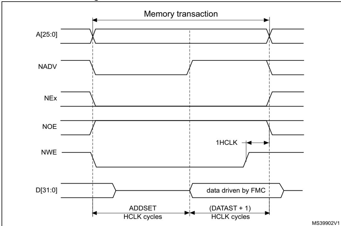
This timing diagram illustrates the signals for a Mode B write access. The signals shown are address A[25:0], address valid (NADV), next address (NEx), output enable (NOE), write enable (NWE), and data D[31:0]. The diagram is divided into three phases: address setup (ADDSET HCLK cycles), data drive (DATAST + 1 HCLK cycles), and a 1HCLK cycle where NWE is toggled. The data is driven by the FMC during the data drive phase. The memory transaction starts when A[25:0] is valid and NADV goes low, and ends when NADV goes high. NEx is active low. NOE is active low. NWE is active low and toggles during the data drive phase. D[31:0] is driven by the FMC during the data drive phase. The main difference from Mode 2 is the timing of the NWE signal, which is toggled during the data drive phase.
The differences with mode 1 are the toggling of NWE and the independent read and write timings when extended mode is set (mode B).
Table 70. FMC_BCRx bitfields (mode 2/B)| Bit number | Bit name | Value to set |
|---|---|---|
| 31:22 | Reserved | 0x000 |
| 21 | WFDIS | As needed |
| 20 | CCLKEN | As needed |
| 19 | CBURSTRW | 0x0 (no effect in Asynchronous mode) |
| 18:16 | CPSIZE | 0x0 (no effect in Asynchronous mode) |
| 15 | ASYNCWAIT | Set to 1 if the memory supports this feature. Otherwise keep at 0. |
| 14 | EXTMOD | 0x1 for mode B, 0x0 for mode 2 |
| 13 | WAITEN | 0x0 (no effect in Asynchronous mode) |
| 12 | WREN | As needed |
| 11 | WAITCFG | Don't care |
| 10 | Reserved | 0x0 |
| 9 | WAITPOL | Meaningful only if bit 15 is 1 |
| 8 | BURSTEN | 0x0 |
| 7 | Reserved | 0x1 |
| 6 | FACCEN | 0x1 |
| 5:4 | MWID | As needed |
| 3:2 | MTYP | 0x2 (NOR flash memory) |
| 1 | MUXEN | 0x0 |
| 0 | MBKEN | 0x1 |
| Bit number | Bit name | Value to set |
|---|---|---|
| 31:30 | Reserved | 0x0 |
| 29:28 | ACCMOD | 0x1 if Extended mode is set |
| 27:24 | DATLAT | Don't care |
| 23:20 | CLKDIV | Don't care |
| 19:16 | BUSTURN | Time between NEx high to NEx low (BUSTURN HCLK). |
| 15:8 | DATAST | Duration of the access second phase (DATAST HCLK cycles) for read accesses. |
| 7:4 | ADDHLD | Don't care |
| 3:0 | ADDSET | Duration of the access first phase (ADDSET HCLK cycles) for read accesses. Minimum value for ADDSET is 0. |
Table 72. FMC_BWTRx bitfields (mode 2/B)
| Bit number | Bit name | Value to set |
|---|---|---|
| 31:30 | Reserved | 0x0 |
| 29:28 | ACCMOD | 0x1 if Extended mode is set |
| 27:24 | DATLAT | Don't care |
| 23:20 | CLKDIV | Don't care |
| 19:16 | BUSTURN | Time between NEx high to NEx low (BUSTURN HCLK). |
| 15:8 | DATAST | Duration of the access second phase (DATAST HCLK cycles) for write accesses. |
| 7:4 | ADDHLD | Don't care |
| 3:0 | ADDSET | Duration of the access first phase (ADDSET HCLK cycles) for write accesses. Minimum value for ADDSET is 0. |
Note: The FMC_BWTRx register is valid only if the Extended mode is set (mode B), otherwise its content is don't care.
Mode C - NOR flash - OE toggling
Figure 45. Mode C read access waveforms
![Timing diagram for Mode C read access waveforms showing address (A[25:0]), NADV, NEx, NOE, NWE, and data (D[31:0]) signals over time. The diagram illustrates the memory transaction phases: ADDSET and DATAST in HCLK cycles. NADV and NEx are active-low signals. NOE is active-low and toggles to enable data output. NWE is active-low and held high. Data is driven by memory during the DATAST phase.](/RM0386-STM32F469-479/200642732810ed80037fe8993cb80d77_img.jpg)
The diagram shows the following signals and timing parameters:
- A[25:0] : Address lines, stable during the memory transaction.
- NADV : Address Valid signal, active-low, goes low at the start and high at the end of the transaction.
- NEx : Address and data latching signal, active-low, goes low at the start and high at the end of the transaction.
- NOE : Output Enable signal, active-low, goes low during the DATAST phase to enable data output.
- NWE : Write Enable signal, active-low, held high throughout the read transaction.
- D[31:0] : Data lines, which are tri-stated during the ADDSET phase and driven by memory during the DATAST phase.
- Memory transaction : The overall duration from the falling edge of NADV/NEx to their rising edge.
- ADDSET HCLK cycles : The duration of the first phase where address and data are latched.
- DATAST HCLK cycles : The duration of the second phase where data is driven by memory.
MS30459V1
Figure 46. Mode C write access waveforms
![Timing diagram for Mode C write access waveforms. The diagram shows the relationship between address (A[25:0]), NADV, NEx, NOE, NWE, and data (D[31:0]) signals over time. A 'Memory transaction' is indicated by a double-headed arrow at the top. The address is stable during the transaction. NADV and NEx are active-low signals that go low at the start and high at the end. NOE is active-low and goes low at the start. NWE is active-low and goes low at the start, then high at the start of the data phase, and then low again at the end. Data is driven by the FMC during the second half of the transaction. Timing parameters ADDSET and (DATAST + 1) are shown in HCLK cycles. A 1HCLK period is also indicated. The diagram is labeled MS39903V1.](/RM0386-STM32F469-479/e77f9abb052e12e90a8480b9e1e4b571_img.jpg)
The differences compared with mode 1 are the toggling of NOE and the independent read and write timings.
Table 73. FMC_BCRx bitfields (mode C)
| Bit number | Bit name | Value to set |
|---|---|---|
| 31:22 | Reserved | 0x000 |
| 21 | WFDIS | As needed |
| 20 | CCLKEN | As needed |
| 19 | CBURSTRW | 0x0 (no effect in Asynchronous mode) |
| 18:16 | CPSIZE | 0x0 (no effect in Asynchronous mode) |
| 15 | ASYNCWAIT | Set to 1 if the memory supports this feature. Otherwise keep at 0. |
| 14 | EXTMOD | 0x1 |
| 13 | WAITEN | 0x0 (no effect in Asynchronous mode) |
| 12 | WREN | As needed |
| 11 | WAITCFG | Don't care |
| 10 | Reserved | 0x0 |
| 9 | WAITPOL | Meaningful only if bit 15 is 1 |
| 8 | BURSTEN | 0x0 |
| 7 | Reserved | 0x1 |
| 6 | FACCEN | 0x1 |
| 5:4 | MWID | As needed |
| Bit number | Bit name | Value to set |
|---|---|---|
| 3:2 | MTYP | 0x02 (NOR flash memory) |
| 1 | MUXEN | 0x0 |
| 0 | MBKEN | 0x1 |
| Bit number | Bit name | Value to set |
|---|---|---|
| 31:30 | Reserved | 0x0 |
| 29:28 | ACCMOD | 0x2 |
| 27:24 | DATLAT | 0x0 |
| 23:20 | CLKDIV | 0x0 |
| 19:16 | BUSTURN | Time between NEx high to NEx low (BUSTURN HCLK). |
| 15:8 | DATAST | Duration of the second access phase (DATAST HCLK cycles) for read accesses. |
| 7:4 | ADDHLD | Don't care |
| 3:0 | ADDSET | Duration of the first access phase (ADDSET HCLK cycles) for read accesses. Minimum value for ADDSET is 0. |
| Bit number | Bit name | Value to set |
|---|---|---|
| 31:30 | Reserved | 0x0 |
| 29:28 | ACCMOD | 0x2 |
| 27:24 | DATLAT | Don't care |
| 23:20 | CLKDIV | Don't care |
| 19:16 | BUSTURN | Time between NEx high to NEx low (BUSTURN HCLK). |
| 15:8 | DATAST | Duration of the second access phase (DATAST HCLK cycles) for write accesses. |
| 7:4 | ADDHLD | Don't care |
| 3:0 | ADDSET | Duration of the first access phase (ADDSET HCLK cycles) for write accesses. Minimum value for ADDSET is 0. |
Mode D - asynchronous access with extended address
Figure 47. Mode D read access waveforms
![Timing diagram for Mode D read access waveforms showing signals A[25:0], NADV, NEx, NOE, NWE, and D[31:0] over time. It defines parameters like Memory transaction, ADDSET, ADDHLD, and DATAST in HCLK cycles.](/RM0386-STM32F469-479/7d1a06ae7a3a857439672eee0b652a39_img.jpg)
This timing diagram illustrates the read access sequence for Mode D. The signals shown are address lines A[25:0], address valid signal NADV, next address signal NEx, output enable signal NOE, write enable signal NWE (held high), and data lines D[31:0]. The sequence starts with a 'Memory transaction' indicated by a double-headed arrow. The address A[25:0] is stable during the transaction. NADV goes low to indicate valid address and returns high. NEx goes low at the start and returns high at the end. NOE goes low to enable data output from memory and returns high. NWE remains high throughout. Data D[31:0] is driven by memory when NOE is low. Timing parameters are defined as follows: ADDSET (HCLK cycles) from the start of the transaction to the falling edge of NADV; ADDHLD (HCLK cycles) from the falling edge of NADV to the falling edge of NOE; and DATAST (HCLK cycles) from the falling edge of NOE to the rising edge of NEx.
MS30461V1
Figure 48. Mode D write access waveforms
![Timing diagram for Mode D write access waveforms showing signals A[25:0], NADV, NEx, NOE, NWE, and D[31:0] over time. It defines parameters like Memory transaction, ADDSET, ADDHLD, and (DATAST + 1) in HCLK cycles.](/RM0386-STM32F469-479/9048b36107c63e1116df1328c16fd30e_img.jpg)
This timing diagram illustrates the write access sequence for Mode D. The signals shown are the same as in Figure 47. The sequence starts with a 'Memory transaction'. Address A[25:0] is stable. NADV goes low and returns high. NEx goes low and returns high. NOE goes low at the start and returns high at the end. NWE goes low to enable data input to memory and returns high. Data D[31:0] is driven by the FMC when NWE is low. Timing parameters are defined as follows: ADDSET (HCLK cycles) from the start of the transaction to the falling edge of NADV; ADDHLD (HCLK cycles) from the falling edge of NADV to the falling edge of NWE; and (DATAST + 1) (HCLK cycles) from the falling edge of NWE to the rising edge of NEx. A 1HCLK cycle interval is also indicated between the rising edge of NWE and the rising edge of NEx.
MS39904V1
The differences with mode 1 are the toggling of NOE that goes on toggling after NADV changes and the independent read and write timings.
Table 76. FMC_BCRx bitfields (mode D)| Bit number | Bit name | Value to set |
|---|---|---|
| 31:22 | Reserved | 0x000 |
| 21 | WFDIS | As needed |
| 20 | CCLKEN | As needed |
| 19 | CBURSTRW | 0x0 (no effect in Asynchronous mode) |
| 18:16 | CPSIZE | 0x0 (no effect in Asynchronous mode) |
| 15 | ASYNCWAIT | Set to 1 if the memory supports this feature. Otherwise keep at 0. |
| 14 | EXTMOD | 0x1 |
| 13 | WAITEN | 0x0 (no effect in Asynchronous mode) |
| 12 | WREN | As needed |
| 11 | WAITCFG | Don't care |
| 10 | Reserved | 0x0 |
| 9 | WAITPOL | Meaningful only if bit 15 is 1 |
| 8 | BURSTEN | 0x0 |
| 7 | Reserved | 0x1 |
| 6 | FACCEN | Set according to memory support |
| 5:4 | MWID | As needed |
| 3:2 | MTYP | As needed |
| 1 | MUXEN | 0x0 |
| 0 | MBKEN | 0x1 |
| Bit number | Bit name | Value to set |
|---|---|---|
| 31:30 | Reserved | 0x0 |
| 29:28 | ACCMOD | 0x3 |
| 27:24 | DATLAT | Don't care |
| 23:20 | CLKDIV | Don't care |
| 19:16 | BUSTURN | Time between NEx high to NEx low (BUSTURN HCLK). |
| 15:8 | DATAST | Duration of the second access phase (DATAST HCLK cycles) for read accesses. |
| 7:4 | ADDHLD | Duration of the middle phase of the read access (ADDHLD HCLK cycles) |
| 3:0 | ADDSET | Duration of the first access phase (ADDSET HCLK cycles) for read accesses. Minimum value for ADDSET is 1. |
Table 78. FMC_BWTRx bitfields (mode D)
| Bit number | Bit name | Value to set |
|---|---|---|
| 31:30 | Reserved | 0x0 |
| 29:28 | ACCMOD | 0x3 |
| 27:24 | DATLAT | Don't care |
| 23:20 | CLKDIV | Don't care |
| 19:16 | BUSTURN | Time between NEx high to NEx low (BUSTURN HCLK). |
| 15:8 | DATAST | Duration of the second access phase (DATAST + 1 HCLK cycles) for write accesses. |
| 7:4 | ADDHLD | Duration of the middle phase of the write access (ADDHLD HCLK cycles) |
| 3:0 | ADDSET | Duration of the first access phase (ADDSET HCLK cycles) for write accesses. Minimum value for ADDSET is 1. |
Muxed mode - multiplexed asynchronous access to NOR flash memory
Figure 49. Muxed read access waveforms
The diagram illustrates the timing for a read access in muxed mode. The signals shown are:
- A[25:16] : Address lines, valid during the first access phase (ADDSET).
- NADV : Address Valid signal, active low, goes low at the start of the transaction and high at the start of the second phase.
- NEx : Address and Data Valid signal, active low, goes low at the start and high at the end of the transaction.
- NOE : Output Enable signal, active low, goes low at the start of the second phase and high at the end.
- NWE : Write Enable signal, active low, held high during read access.
- AD[15:0] : Multiplexed address/data lines. They carry 'Lower address' during the first phase and 'data driven by memory' during the second phase.
Timing parameters are defined as follows:
- ADDSET : Duration of the first access phase in HCLK cycles.
- ADDHLD : Duration of the middle phase in HCLK cycles.
- DATAST : Duration of the second access phase in HCLK cycles.
The total 'Memory transaction' duration is the sum of ADDSET, ADDHLD, and DATAST HCLK cycles. The diagram is identified by the code ai15568.
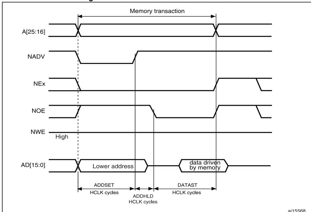
Figure 50. Muxed write access waveforms
![Timing diagram for Muxed write access waveforms showing signals A[25:16], NADV, NEx, NOE, NWE, and AD[15:0] over time. The diagram illustrates the sequence of a memory transaction: address setup (ADDSET), address hold (ADDHLD), and data drive (DATAST + 1). The AD[15:0] bus is shown driving 'Lower address' and 'data driven by FMC'. A 1HCLK cycle is also indicated.](/RM0386-STM32F469-479/3e3b0d2b0dcf80f0c4e84f57bd2c1433_img.jpg)
The diagram shows the timing for a muxed write access. The signals shown are:
- A[25:16] : Address lines, valid during the ADDSET and ADDHLD phases.
- NADV : Address Valid signal, active low. It goes low at the start of the transaction and high at the start of the data drive phase.
- NEx : Address/Command External signal, active low. It goes low at the start and high at the end of the transaction.
- NOE : Output Enable signal, active low. It is high throughout the write transaction.
- NWE : Write Enable signal, active low. It goes low at the start of the data drive phase and high at the end.
- AD[15:0] : Data bus. It drives 'Lower address' during the first phase and 'data driven by FMC' during the second phase.
Timing parameters are defined in HCLK cycles:
- ADDSET : Address setup time.
- ADDHLD : Address hold time.
- (DATAST + 1) : Data setup time plus one HCLK cycle.
- 1HCLK : One system clock cycle.
Reference: MS39905V2
The difference with mode D is the drive of the lower address byte(s) on the data bus.
Table 79. FMC_BCRx bitfields (Muxed mode)
| Bit number | Bit name | Value to set |
|---|---|---|
| 31:22 | Reserved | 0x000 |
| 21 | WFDIS | As needed |
| 20 | CCLKEN | As needed |
| 19 | CBURSTRW | 0x0 (no effect in Asynchronous mode) |
| 18:16 | CPSIZE | 0x0 (no effect in Asynchronous mode) |
| 15 | ASYNCWAIT | Set to 1 if the memory supports this feature. Otherwise keep at 0. |
| 14 | EXTMOD | 0x0 |
| 13 | WAITEN | 0x0 (no effect in Asynchronous mode) |
| 12 | WREN | As needed |
| 11 | WAITCFG | Don't care |
| 10 | Reserved | 0x0 |
| 9 | WAITPOL | Meaningful only if bit 15 is 1 |
| 8 | BURSTEN | 0x0 |
| 7 | Reserved | 0x1 |
| 6 | FACCEN | 0x1 |
| 5:4 | MWID | As needed |
| Bit number | Bit name | Value to set |
|---|---|---|
| 3:2 | MTYP | 0x2 (NOR flash memory) or 0x1(PSRAM) |
| 1 | MUXEN | 0x1 |
| 0 | MBKEN | 0x1 |
| Bit number | Bit name | Value to set |
|---|---|---|
| 31:30 | Reserved | 0x0 |
| 29:28 | ACCMOD | 0x0 |
| 27:24 | DATLAT | Don't care |
| 23:20 | CLKDIV | Don't care |
| 19:16 | BUSTURN | Time between NEx high to NEx low (BUSTURN HCLK). |
| 15:8 | DATAST | Duration of the second access phase (DATAST HCLK cycles for read accesses and DATAST+1 HCLK cycles for write accesses). |
| 7:4 | ADDHLD | Duration of the middle phase of the access (ADDHLD HCLK cycles). |
| 3:0 | ADDSET | Duration of the first access phase (ADDSET HCLK cycles). Minimum value for ADDSET is 1. |
WAIT management in asynchronous accesses
If the asynchronous memory asserts the WAIT signal to indicate that it is not yet ready to accept or to provide data, the ASYNCWAIT bit has to be set in FMC_BCRx register.
If the WAIT signal is active (high or low depending on the WAITPOL bit), the second access phase (Data setup phase), programmed by the DATAST bits, is extended until WAIT becomes inactive. Unlike the data setup phase, the first access phases (Address setup and Address hold phases), programmed by the ADDSET and ADDHLD bits, are not WAIT sensitive and so they are not prolonged.
The data setup phase must be programmed so that WAIT can be detected 4 HCLK cycles before the end of the memory transaction. The following cases must be considered:
- 1. The memory asserts the WAIT signal aligned to NOE/NWE which toggles:
- 2. The memory asserts the WAIT signal aligned to NEx (or NOE/NWE not toggling):
if
then:
otherwise
where \( \text{max\_wait\_assertion\_time} \) is the maximum time taken by the memory to assert the WAIT signal once NEx/NOE/NWE is low.
Figure 51 and Figure 52 show the number of HCLK clock cycles that are added to the memory access phase after WAIT is released by the asynchronous memory (independently of the above cases).
Figure 51. Asynchronous wait during a read access waveforms
![Timing diagram for asynchronous wait during a read access. The diagram shows five signal lines over time: A[25:0] (Address), NEx (Next), NWAIT (Next Wait), NOE (Next Output Enable), and D[15:0] (Data). The 'Memory transaction' starts when A[25:0] is stable and NEx goes low. It is divided into 'address phase' (from start to when NOE goes low) and 'data setup phase' (from when NOE goes low to when data is driven). NWAIT is shown as 'don't care' during the address phase and becomes active (low) during the data setup phase. NOE goes low at the start of the data setup phase and goes high when data is driven. D[15:0] is driven by memory during the data setup phase, starting 4 HCLK cycles before the transaction ends. The transaction ends when NEx goes high.](/RM0386-STM32F469-479/f1329098c879f36abec71d468767ccdb_img.jpg)
- 1. NWAIT polarity depends on WAITPOL bit setting in FMC_BCRx register.
Figure 52. Asynchronous wait during a write access waveforms
![Timing diagram for asynchronous wait during a write access. The diagram shows five signals over time: A[25:0] (Address), NEx (Next), NWAIT (Wait), NWE (Write Enable), and D[15:0] (Data). The transaction is divided into an 'address phase' and a 'data setup phase'. NEx is active low. NWAIT is shown as 'don't care' during the address phase and 'don't care' during the data setup phase. NWE is active low. D[15:0] is driven by the FMC. Timing parameters include 1HCLK (one HCLK cycle) and 3HCLK (three HCLK cycles). The diagram is labeled MSV40168V1.](/RM0386-STM32F469-479/2b93d528fd010ad8f6201ab02e16c78d_img.jpg)
1. NWAIT polarity depends on WAITPOL bit setting in FMC_BCRx register.
12.6.5 Synchronous transactions
The memory clock, FMC_CLK, is a submultiple of HCLK. It depends on the value of CLKDIV and the MWID/ AHB data size, following the formula given below:
If MWID is 16 or 8-bit, the FMC_CLK divider ratio is always defined by the programmed CLKDIV value.
If MWID is 32-bit, the FMC_CLK divider ratio depends also on AHB data size.
Example:
- • If CLKDIV=1, MWID = 32 bits, AHB data size=8 bits, FMC_CLK=HCLK/4.
- • If CLKDIV=1, MWID = 16 bits, AHB data size=8 bits, FMC_CLK=HCLK/2.
NOR flash memories specify a minimum time from NADV assertion to CLK high. To meet this constraint, the FMC does not issue the clock to the memory during the first internal clock cycle of the synchronous access (before NADV assertion). This guarantees that the rising edge of the memory clock occurs in the middle of the NADV low pulse.
Data latency versus NOR memory latency
The data latency is the number of cycles to wait before sampling the data. The DATLAT value must be consistent with the latency value specified in the NOR flash configuration register. The FMC does not include the clock cycle when NADV is low in the data latency count.
Caution: Some NOR flash memories include the NADV Low cycle in the data latency count, so that the exact relation between the NOR flash latency and the FMC DATLAT parameter can be either:
- • NOR flash latency = (DATLAT + 2) CLK clock cycles
- • or NOR flash latency = (DATLAT + 3) CLK clock cycles
Some recent memories assert NWAIT during the latency phase. In such cases DATLAT can be set to its minimum value. As a result, the FMC samples the data and waits long enough to evaluate if the data are valid. Thus the FMC detects when the memory exits latency and real data are processed.
Other memories do not assert NWAIT during latency. In this case the latency must be set correctly for both the FMC and the memory, otherwise invalid data are mistaken for good data, or valid data are lost in the initial phase of the memory access.
Single-burst transfer
When the selected bank is configured in Burst mode for synchronous accesses, if for example an AHB single-burst transaction is requested on 16-bit memories, the FMC performs a burst transaction of length 1 (if the AHB transfer is 16 bits), or length 2 (if the AHB transfer is 32 bits) and de-assert the chip select signal when the last data is strobed.
Such transfers are not the most efficient in terms of cycles compared to asynchronous read operations. Nevertheless, a random asynchronous access would first require to re-program the memory access mode, which would altogether last longer.
Cross boundary page for CellularRAM™ 1.5
CellularRAM™ 1.5 does not allow burst access to cross the page boundary. The FMC controller is used to split automatically the burst access when the memory page size is reached by configuring the CPSIZE bits in the FMC_BCR1 register following the memory page size.
Wait management
For synchronous NOR flash memories, NWAIT is evaluated after the programmed latency period, which corresponds to (DATLAT+2) CLK clock cycles.
If NWAIT is active (low level when WAITPOL = 0, high level when WAITPOL = 1), wait states are inserted until NWAIT is inactive (high level when WAITPOL = 0, low level when WAITPOL = 1).
When NWAIT is inactive, the data is considered valid either immediately (bit WAITCFG = 1) or on the next clock edge (bit WAITCFG = 0).
During wait-state insertion via the NWAIT signal, the controller continues to send clock pulses to the memory, keeping the chip select and output enable signals valid. It does not consider the data as valid.
In Burst mode, there are two timing configurations for the NOR flash NWAIT signal:
- • The flash memory asserts the NWAIT signal one data cycle before the wait state (default after reset).
- • The flash memory asserts the NWAIT signal during the wait state
The FMC supports both NOR flash wait state configurations, for each chip select, thanks to the WAITCFG bit in the FMC_BCRx registers (x = 0..3).
Figure 53. Wait configuration waveforms
![Timing diagram for Figure 53 showing wait configuration waveforms. It includes signals HCLK, CLK, A[25:16], NADV, NWAIT (WAITCFG = 0), NWAIT (WAITCFG = 1), and A/D[15:0]. A memory transaction is shown as a burst of 4 half words. The diagram illustrates the effect of inserting a wait state when WAITCFG is 1.](/RM0386-STM32F469-479/ccd2a65aecf8ea232334db16bbde116e_img.jpg)
Figure 53 shows the timing for wait configuration. The signals shown are HCLK, CLK, A[25:16], NADV, NWAIT (WAITCFG = 0), NWAIT (WAITCFG = 1), and A/D[15:0]. A memory transaction is defined as a burst of 4 half words. The diagram shows the address A[25:16] being latched on the rising edge of CLK. The NADV signal is active low. The NWAIT signal is shown for two configurations: WAITCFG = 0 and WAITCFG = 1. When WAITCFG = 1, an inserted wait state is shown, which extends the data burst. The data is transferred in half words, and the address is latched on the rising edge of CLK.
Figure 54. Synchronous multiplexed read mode waveforms - NOR, PSRAM (CRAM)
![Timing diagram for Figure 54 showing synchronous multiplexed read mode waveforms for NOR, PSRAM, and CRAM. It includes signals HCLK, CLK, A[25:16], NEx, NOE, NWE, NADV, NWAIT (WAITCFG = 0), and A/D[15:0]. A memory transaction is shown as a burst of 4 half words. The diagram illustrates the timing for data strobes and the effect of inserting a wait state.](/RM0386-STM32F469-479/e8fb0881b45afc635f27ef8b5b92284f_img.jpg)
Figure 54 shows the timing for synchronous multiplexed read mode. The signals shown are HCLK, CLK, A[25:16], NEx, NOE, NWE, NADV, NWAIT (WAITCFG = 0), and A/D[15:0]. A memory transaction is defined as a burst of 4 half words. The address A[25:16] is latched on the rising edge of CLK. The NEx signal is active low. The NOE signal is active low. The NWE signal is high. The NADV signal is active low. The NWAIT signal is shown for WAITCFG = 0. The data is transferred in half words, and the address is latched on the rising edge of CLK. The data strobes are shown on the falling edge of CLK. The timing for the data burst is (DATLAT + 2) CLK cycles. An inserted wait state is shown, which extends the data burst.
- 1. Byte lane outputs (NBL are not shown; for NOR access, they are held high, and, for PSRAM (CRAM) access, they are held low.
| Bit number | Bit name | Value to set |
|---|---|---|
| 31:22 | Reserved | 0x000 |
| 21 | WFDIS | As needed |
| 20 | CCLKEN | As needed |
| 19 | CBURSTRW | No effect on synchronous read |
| 18:16 | CPSIZE | 0x0 (no effect in Asynchronous mode) |
| 15 | ASYNCWAIT | 0x0 |
| 14 | EXTMOD | 0x0 |
| 13 | WAITEN | To be set to 1 if the memory supports this feature, to be kept at 0 otherwise |
| 12 | WREN | No effect on synchronous read |
| 11 | WAITCFG | To be set according to memory |
| 10 | Reserved | 0x0 |
| 9 | WAITPOL | To be set according to memory |
| 8 | BURSTEN | 0x1 |
| 7 | Reserved | 0x1 |
| 6 | FACCEN | Set according to memory support (NOR flash memory) |
| 5-4 | MWID | As needed |
| 3-2 | MTYP | 0x1 or 0x2 |
| 1 | MUXEN | As needed |
| 0 | MBKEN | 0x1 |
| Bit number | Bit name | Value to set |
|---|---|---|
| 31:30 | Reserved | 0x0 |
| 29:28 | ACCMOD | 0x0 |
| 27-24 | DATLAT | Data latency |
| 27-24 | DATLAT | Data latency |
| 23-20 | CLKDIV | 0x0 to get CLK = HCLK (Not supported) 0x1 to get CLK = 2 × HCLK .. |
| 19-16 | BUSTURN | Time between NEx high to NEx low (BUSTURN HCLK). |
| 15-8 | DATAST | Don't care |
| 7-4 | ADDHLD | Don't care |
| 3-0 | ADDSET | Don't care |
Figure 55. Synchronous multiplexed write mode waveforms - PSRAM (CRAM)
![Timing diagram for synchronous multiplexed write mode waveforms. The diagram shows the relationship between HCLK, CLK, address lines A[25:16], active-low signals NEx, NOE, NWE, NADV, NWAIT, and data lines A/D[15:0]. A memory transaction is defined as a burst of 2 half words. The address is latched on the rising edge of CLK. Data is written on the rising edge of CLK. The diagram shows the address being latched, followed by a wait state, and then two data half-words being written. The timing parameters (DATLAT + 2) and inserted wait state are indicated.](/RM0386-STM32F469-479/9dc1e8ca0e82453835b0bbc643e510c2_img.jpg)
Timing diagram showing waveforms for HCLK, CLK, A[25:16], NEx, NOE, NWE, NADV, NWAIT (WAITCFG = 0), and A/D[15:0].
Key signals and timing parameters:
- HCLK: System clock.
- CLK: Memory clock.
- A[25:16]: Address lines, showing
addr[25:16]. - NEx: Active-low chip select.
- NOE: Active-low output enable (Hi-Z).
- NWE: Active-low write enable.
- NADV: Active-low address valid.
- NWAIT (WAITCFG = 0): Active-low wait signal.
- A/D[15:0]: Data lines, showing
Addr[15:0]anddata. - Memory transaction = burst of 2 half words.
- (DATLAT + 2) CLK cycles: Time between address latching and data write.
- inserted wait state: A wait state inserted between data half-words.
- 1 clock: One CLK cycle.
ai14731f
- 1. The memory must issue NWAIT signal one cycle in advance, accordingly WAITCFG must be programmed to 0.
- 2. Byte Lane (NBL) outputs are not shown, they are held low while NEx is active.
Table 83. FMC_BCRx bitfields (Synchronous multiplexed write mode)
| Bit number | Bit name | Value to set |
|---|---|---|
| 31:22 | Reserved | 0x000 |
| 21 | WFDIS | As needed |
| 20 | CCLKEN | As needed |
| 19 | CBURSTRW | 0x1 |
| 18:16 | CPSIZE | As needed (0x1 for CRAM 1.5) |
| 15 | ASYNCWAIT | 0x0 |
| 14 | EXTMOD | 0x0 |
| 13 | WAITEN | To be set to 1 if the memory supports this feature, to be kept at 0 otherwise. |
| Bit number | Bit name | Value to set |
|---|---|---|
| 12 | WREN | 0x1 |
| 11 | WAITCFG | 0x0 |
| 10 | Reserved | 0x0 |
| 9 | WAITPOL | to be set according to memory |
| 8 | BURSTEN | no effect on synchronous write |
| 7 | Reserved | 0x1 |
| 6 | FACCEN | Set according to memory support |
| 5-4 | MWID | As needed |
| 3-2 | MTYP | 0x1 |
| 1 | MUXEN | As needed |
| 0 | MBKEN | 0x1 |
| Bit number | Bit name | Value to set |
|---|---|---|
| 31-30 | Reserved | 0x0 |
| 29:28 | ACCMOD | 0x0 |
| 27-24 | DATLAT | Data latency |
| 23-20 | CLKDIV | 0x0 to get CLK = HCLK (not supported) 0x1 to get CLK = 2 × HCLK |
| 19-16 | BUSTURN | Time between NEx high to NEx low (BUSTURN HCLK). |
| 15-8 | DATAST | Don't care |
| 7-4 | ADDHLD | Don't care |
| 3-0 | ADDSET | Don't care |
12.6.6 NOR/PSRAM controller registers
SRAM/NOR-flash chip-select control register for bank x (FMC_BCRx)
Address offset: \( 0x00 + 0x8 * (x - 1) \) , ( \( x = 1 \) to \( 4 \) )
Reset value: \( 0x0000\ 30DB \) , \( 0x0000\ 30D2 \) , \( 0x0000\ 30D2 \) , \( 0x0000\ 30D2 \)
This register contains the control information of each memory bank, used for SRAMs, PSRAM and NOR flash memories.
| 31 | 30 | 29 | 28 | 27 | 26 | 25 | 24 | 23 | 22 | 21 | 20 | 19 | 18 | 17 | 16 |
|---|---|---|---|---|---|---|---|---|---|---|---|---|---|---|---|
| Res. | Res. | Res. | Res. | Res. | Res. | Res. | Res. | Res. | Res. | WFDIS | CCLK EN | CBURST RW | CPSIZE[2:0] | ||
| rw | rw | rw | rw | rw | rw | ||||||||||
| 15 | 14 | 13 | 12 | 11 | 10 | 9 | 8 | 7 | 6 | 5 | 4 | 3 | 2 | 1 | 0 |
|---|---|---|---|---|---|---|---|---|---|---|---|---|---|---|---|
| ASYNC WAIT | EXT MOD | WAIT EN | WREN | WAIT CFG | Res. | WAIT POL | BURST EN | Res. | FACC EN | MWID[1:0] | MTYP[1:0] | MUX EN | MBK EN | ||
| rw | rw | rw | rw | rw | rw | rw | rw | rw | rw | rw | rw | rw | rw | ||
Bits 31:22 Reserved, must be kept at reset value.
Bit 21 WFDIS: Write FIFO disable
This bit disables the Write FIFO used by the FMC controller.
0: Write FIFO enabled (Default after reset)
1: Write FIFO disabled
Note: The WFDIS bit of the FMC_BCR2..4 registers is don't care. It is only enabled through the FMC_BCR1 register.
Bit 20 CCLKEN: Continuous clock enable
This bit enables the FMC_CLK clock output to external memory devices.
0: The FMC_CLK is only generated during the synchronous memory access (read/write transaction). The FMC_CLK clock ratio is specified by the programmed CLKDIV value in the FMC_BCRx register (default after reset).
1: The FMC_CLK is generated continuously during asynchronous and synchronous access. The FMC_CLK clock is activated when the CCLKEN is set.
Note: The CCLKEN bit of the FMC_BCR2..4 registers is don't care. It is only enabled through the FMC_BCR1 register. Bank 1 must be configured in Synchronous mode to generate the FMC_CLK continuous clock.
Note: If CCLKEN bit is set, the FMC_CLK clock ratio is specified by CLKDIV value in the FMC_BTR1 register. CLKDIV in FMC_BWTR1 is don't care.
Note: If the Synchronous mode is used and CCLKEN bit is set, the synchronous memories connected to other banks than Bank 1 are clocked by the same clock (the CLKDIV value in the FMC_BTR2..4 and FMC_BWTR2..4 registers for other banks has no effect.)
Bit 19 CBURSTRW: Write burst enable
For PSRAM (CRAM) operating in Burst mode, the bit enables synchronous accesses during write operations. The enable bit for synchronous read accesses is the BURSTEN bit in the FMC_BCRx register.
0: Write operations are always performed in Asynchronous mode.
1: Write operations are performed in Synchronous mode.
Bits 18:16 CPSIZE[2:0] : CRAM page sizeThese are used for CellularRAM™ 1.5 which does not allow burst access to cross the address boundaries between pages. When these bits are configured, the FMC controller splits automatically the burst access when the memory page size is reached (refer to memory datasheet for page size).
000: No burst split when crossing page boundary (default after reset)
001: 128 bytes
010: 256 bytes
011: 512 bytes
100: 1024 bytes
Others: Reserved, must not be used
Bit 15 ASYNCWAIT : Wait signal during asynchronous transfersThis bit enables/disables the FMC to use the wait signal even during an asynchronous protocol.
0: NWAIT signal is not taken in to account when running an asynchronous protocol (default after reset).
1: NWAIT signal is taken in to account when running an asynchronous protocol.
Bit 14 EXTMOD : Extended mode enableThis bit enables the FMC to program the write timings for non multiplexed asynchronous accesses inside the FMC_BWTR register, thus resulting in different timings for read and write operations.
0: values inside FMC_BWTR register are not taken into account (default after reset)
1: values inside FMC_BWTR register are taken into account
Note: When the Extended mode is disabled, the FMC can operate in mode 1 or mode 2 as follows:
- – Mode 1 is the default mode when the SRAM/PSRAM memory type is selected (MTYP = 0x0 or 0x01)
- – Mode 2 is the default mode when the NOR memory type is selected (MTYP = 0x10).
This bit enables/disables wait-state insertion via the NWAIT signal when accessing the memory in Synchronous mode.
0: NWAIT signal is disabled (its level not taken into account, no wait state inserted after the programmed flash latency period).
1: NWAIT signal is enabled (its level is taken into account after the programmed latency period to insert wait states if asserted) (default after reset).
Bit 12 WREN : Write enable bitThis bit indicates whether write operations are enabled/disabled in the bank by the FMC.
0: Write operations are disabled in the bank by the FMC, an AHB error is reported.
1: Write operations are enabled for the bank by the FMC (default after reset).
Bit 11 WAITCFG : Wait timing configurationThe NWAIT signal indicates whether the data from the memory are valid or if a wait state must be inserted when accessing the memory in Synchronous mode. This configuration bit determines if NWAIT is asserted by the memory one clock cycle before the wait state or during the wait state:
0: NWAIT signal is active one data cycle before wait state (default after reset).
1: NWAIT signal is active during wait state (not used for PSRAM).
Bit 10 Reserved, must be kept at reset value.
Bit 9 WAITPOL : Wait signal polarity bitDefines the polarity of the wait signal from memory used for either in Synchronous or Asynchronous mode.
0: NWAIT active low (default after reset)
1: NWAIT active high
Bit 8 BURSTEN : Burst enable bit
This bit enables/disables synchronous accesses during read operations. It is valid only for synchronous memories operating in Burst mode.
0: Burst mode disabled (default after reset). Read accesses are performed in Asynchronous mode.
1: Burst mode enable. Read accesses are performed in Synchronous mode.
Bit 7 Reserved, must be kept at reset value.
Bit 6 FACCEN : Flash access enable
Enables NOR flash memory access operations.
0: Corresponding NOR flash memory access is disabled.
1: Corresponding NOR flash memory access is enabled (default after reset).
Bits 5:4 MWID[1:0] : Memory data bus width
Defines the external memory device width, valid for all type of memories.
00: 8 bits
01: 16 bits (default after reset)
10: 32 bits
11: reserved
Bits 3:2 MTYP[1:0] : Memory type
Defines the type of external memory attached to the corresponding memory bank.
00: SRAM (default after reset for Bank 2...4)
01: PSRAM (CRAM)
10: NOR flash/OneNAND flash (default after reset for Bank 1)
11: reserved
Bit 1 MUXEN : Address/data multiplexing enable bit
When this bit is set, the address and data values are multiplexed on the data bus, valid only with NOR and PSRAM memories:
0: Address/data non multiplexed
1: Address/data multiplexed on databus (default after reset)
Bit 0 MBKEN : Memory bank enable bit
Enables the memory bank. After reset Bank1 is enabled, all others are disabled. Accessing a disabled bank causes an ERROR on AHB bus.
0: Corresponding memory bank is disabled.
1: Corresponding memory bank is enabled.
SRAM/NOR-flash chip-select timing register for bank x (FMC_BTRx)
Address offset: \( 0x04 + 0x8 * (x - 1) \) , ( \( x = 1 \) to \( 4 \) )
Reset value: 0x0FFF FFFF
This register contains the control information of each memory bank, used for SRAMs, PSRAM and NOR flash memories. If the EXTMOD bit is set in the FMC_BCRx register, then this register is partitioned for write and read access, that is, 2 registers are available: one to
configure read accesses (this register) and one to configure write accesses (FMC_BWTRx registers).
| 31 | 30 | 29 | 28 | 27 | 26 | 25 | 24 | 23 | 22 | 21 | 20 | 19 | 18 | 17 | 16 |
|---|---|---|---|---|---|---|---|---|---|---|---|---|---|---|---|
| Res. | Res. | ACCMOD[1:0] | DATLAT[3:0] | CLKDIV[3:0] | BURSTN[3:0] | ||||||||||
| rw | rw | rw | rw | rw | rw | rw | rw | rw | rw | rw | rw | rw | rw | ||
| 15 | 14 | 13 | 12 | 11 | 10 | 9 | 8 | 7 | 6 | 5 | 4 | 3 | 2 | 1 | 0 |
| DATAST[7:0] | ADDHLD[3:0] | ADDSET[3:0] | |||||||||||||
| rw | rw | rw | rw | rw | rw | rw | rw | rw | rw | rw | rw | rw | rw | rw | rw |
Bits 31:30 Reserved, must be kept at reset value.
Bits 29:28 ACCMOD[1:0] : Access mode
Specifies the asynchronous access modes as shown in the timing diagrams. These bits are taken into account only when the EXTMOD bit in the FMC_BCRx register is 1.
- 00: Access mode A
- 01: Access mode B
- 10: Access mode C
- 11: Access mode D
Bits 27:24 DATLAT[3:0] : (see note below bit descriptions): Data latency for synchronous memory
For synchronous access with read/write Burst mode enabled (BURSTEN / CBURSTRW bits set), defines the number of memory clock cycles (+2) to issue to the memory before reading/writing the first data:
This timing parameter is not expressed in HCLK periods, but in FMC_CLK periods.
For asynchronous access, this value is don't care.
- 0000: Data latency of 2 CLK clock cycles for first burst access
- 1111: Data latency of 17 CLK clock cycles for first burst access (default value after reset)
Bits 23:20 CLKDIV[3:0] : Clock divide ratio (for FMC_CLK signal)
Defines the period of FMC_CLK clock output signal, expressed in number of HCLK cycles:
- 0000: Reserved
- 0001: FMC_CLK period = 2 × HCLK periods
- 0010: FMC_CLK period = 3 × HCLK periods
- 1111: FMC_CLK period = 16 × HCLK periods (default value after reset)
In asynchronous NOR flash, SRAM or PSRAM accesses, this value is don't care.
Note: Refer to Section 12.6.5: Synchronous transactions for FMC_CLK divider ratio formula
Bits 19:16 BUSTURN[3:0] : Bus turnaround phase durationThese bits are written by software to add a delay at the end of a write-to-read (and read-to-write) transaction. This delay enables to match the minimum time between consecutive transactions ( \( t_{\text{EHEL}} \) from NEx high to NEx low) and the maximum time needed by the memory to free the data bus after a read access ( \( t_{\text{EHQZ}} \) ). The programmed bus turnaround delay is inserted between an asynchronous read (muxed or mode D) or write transaction and any other asynchronous /synchronous read or write to or from a static bank. The bank can be the same or different in case of read, in case of write the bank can be different except for muxed or mode D.
In some cases, whatever the programmed BUSTURN values, the bus turnaround delay is fixed as follows:
- • The bus turnaround delay is not inserted between two consecutive asynchronous write transfers to the same static memory bank except for muxed mode and mode D.
- • There is a bus turnaround delay of 1 HCLK clock cycle between:
- – Two consecutive asynchronous read transfers to the same static memory bank except for muxed mode and mode D.
- – An asynchronous read to an asynchronous or synchronous write to any static bank or dynamic bank except for muxed mode and mode D.
- – An asynchronous (modes 1, 2, A, B or C) read and a read from another static bank.
- • There is a bus turnaround delay of 2 HCLK clock cycle between:
- – Two consecutive synchronous writes (burst or single) to the same bank.
- – A synchronous write (burst or single) access and an asynchronous write or read transfer to or from static memory bank (the bank can be the same or different for the case of read).
- – Two consecutive synchronous reads (burst or single) followed by any synchronous/asynchronous read or write from/to another static memory bank.
- • There is a bus turnaround delay of 3 HCLK clock cycle between:
- – Two consecutive synchronous writes (burst or single) to different static bank.
- – A synchronous write (burst or single) access and a synchronous read from the same or a different bank.
0000: BUSTURN phase duration = 0 HCLK clock cycle added
...
1111: BUSTURN phase duration = 15 x HCLK clock cycles added (default value after reset)
Bits 15:8 DATAST[7:0] : Data-phase durationThese bits are written by software to define the duration of the data phase (refer to Figure 38 to Figure 50 ), used in asynchronous accesses:
0000 0000: Reserved
0000 0001: DATAST phase duration = 1 × HCLK clock cycles
0000 0010: DATAST phase duration = 2 × HCLK clock cycles
...
1111 1111: DATAST phase duration = 255 × HCLK clock cycles (default value after reset)
For each memory type and access mode data-phase duration, refer to the respective figure ( Figure 38 to Figure 50 ).
Example: Mode 1, write access, DATAST=1: Data-phase duration= DATAST+1 = 2 HCLK clock cycles.
Note: In synchronous accesses, this value is don't care.
Bits 7:4 ADDHLD[3:0] : Address-hold phase durationThese bits are written by software to define the duration of the address hold phase (refer to Figure 38 to Figure 50 ), used in mode D or multiplexed accesses:
0000: Reserved
0001: ADDHLD phase duration = 1 × HCLK clock cycle
0010: ADDHLD phase duration = 2 × HCLK clock cycle
...
1111: ADDHLD phase duration = 15 × HCLK clock cycles (default value after reset)
For each access mode address-hold phase duration, refer to the respective figure ( Figure 38 to Figure 50 ).
Note: In synchronous accesses, this value is not used, the address hold phase is always 1 memory clock period duration.
Bits 3:0 ADDSET[3:0] : Address setup phase durationThese bits are written by software to define the duration of the address setup phase (refer to Figure 38 to Figure 50 ), used in SRAMs, ROMs, asynchronous NOR flash and PSRAM:
0000: ADDSET phase duration = 0 × HCLK clock cycle
...
1111: ADDSET phase duration = 15 × HCLK clock cycles (default value after reset)
For each access mode address setup phase duration, refer to the respective figure ( Figure 38 to Figure 50 ).
Note: In synchronous accesses, this value is don't care.
In Muxed mode or mode D, the minimum value for ADDSET is 1.
In mode 1 and PSRAM memory, the minimum value for ADDSET is 1.
Note: PSRAMs (CRAMs) have a variable latency due to internal refresh. Therefore these memories issue the NWAIT signal during the whole latency phase to prolong the latency as needed.
With PSRAMs (CRAMs) the filled DATLAT must be set to 0, so that the FMC exits its latency phase soon and starts sampling NWAIT from memory, then starts to read or write when the memory is ready.
This method can be used also with the latest generation of synchronous flash memories that issue the NWAIT signal, unlike older flash memories (check the datasheet of the specific flash memory being used).
SRAM/NOR-flash write timing registers x (FMC_BWTRx)
Address offset: 0x104 + 0x8 * (x - 1), (x = 1 to 4)
Reset value: 0x0FFF FFFF
This register contains the control information of each memory bank. It is used for SRAMs, PSRAMs and NOR flash memories. When the EXTMOD bit is set in the FMC_BCRx register, then this register is active for write access.
| 31 | 30 | 29 | 28 | 27 | 26 | 25 | 24 | 23 | 22 | 21 | 20 | 19 | 18 | 17 | 16 |
|---|---|---|---|---|---|---|---|---|---|---|---|---|---|---|---|
| Res | Res | ACCMOD[1:0] | Res | Res | Res | Res | Res | Res | Res | Res | BUSTURN[3:0] | ||||
| rw | rw | rw | rw | rw | rw | ||||||||||
| 15 | 14 | 13 | 12 | 11 | 10 | 9 | 8 | 7 | 6 | 5 | 4 | 3 | 2 | 1 | 0 |
| DATAST[7:0] | ADDHLD[3:0] | ADDSET[3:0] | |||||||||||||
| rw | rw | rw | rw | rw | rw | rw | rw | rw | rw | rw | rw | rw | rw | rw | rw |
Bits 31:30 Reserved, must be kept at reset value.
Bits 29:28 ACCMOD[1:0] : Access mode.
Specifies the asynchronous access modes as shown in the next timing diagrams. These bits are taken into account only when the EXTMOD bit in the FMC_BCRx register is 1.
00: Access mode A
01: Access mode B
10: Access mode C
11: Access mode D
Bits 27:20 Reserved, must be kept at reset value.
Bits 19:16 BUSTURN[3:0] : Bus turnaround phase duration
The programmed bus turnaround delay is inserted between an asynchronous write transfer and any other asynchronous /synchronous read or write transfer to or from a static bank. The bank can be the same or different in case of read, in case of write the bank can be different except for muxed or mode D.
In some cases, whatever the programmed BUSTURN values, the bus turnaround delay is fixed as follows:
- • The bus turnaround delay is not inserted between two consecutive asynchronous write transfers to the same static memory bank except for muxed and D modes.
- • There is a bus turnaround delay of 2 HCLK clock cycle between:
- –Two consecutive synchronous writes (burst or single) to the same bank.
- –A synchronous write (burst or single) transfer and an asynchronous write or read transfer to or from static memory bank.
- • There is a bus turnaround delay of 3 HCLK clock cycle between:
- –Two consecutive synchronous writes (burst or single) to different static bank.
- –A synchronous write (burst or single) transfer and a synchronous read from the same or a different bank.
0000: BUSTURN phase duration = 0 HCLK clock cycle added
...
1111: BUSTURN phase duration = 15 HCLK clock cycles added (default value after reset)
Bits 15:8 DATAST[7:0] : Data-phase duration.
These bits are written by software to define the duration of the data phase (refer to Figure 38 to Figure 50 ), used in asynchronous SRAM, PSRAM and NOR flash memory accesses:
0000 0000: Reserved
0000 0001: DATAST phase duration = 1 × HCLK clock cycles
0000 0010: DATAST phase duration = 2 × HCLK clock cycles
...
1111 1111: DATAST phase duration = 255 × HCLK clock cycles (default value after reset)
Bits 7:4 ADDHLD[3:0] : Address-hold phase duration.
These bits are written by software to define the duration of the address hold phase (refer to Figure 47 to Figure 50 ), used in asynchronous multiplexed accesses:
0000: Reserved
0001: ADDHLD phase duration = 1 × HCLK clock cycle
0010: ADDHLD phase duration = 2 × HCLK clock cycle
...
1111: ADDHLD phase duration = 15 × HCLK clock cycles (default value after reset)
Note: In synchronous NOR flash accesses, this value is not used, the address hold phase is always 1 flash clock period duration.
Bits 3:0 ADDSET[3:0] : Address setup phase duration.
These bits are written by software to define the duration of the address setup phase in HCLK cycles (refer to Figure 38 to Figure 50 ), used in asynchronous accesses:
0000: ADDSET phase duration = 0 × HCLK clock cycle
...
1111: ADDSET phase duration = 15 × HCLK clock cycles (default value after reset)
Note: In synchronous accesses, this value is not used, the address setup phase is always 1 flash clock period duration. In muxed mode, the minimum ADDSET value is 1.
12.7 NAND flash controller
The FMC generates the appropriate signal timings to drive the following types of device:
- • 8- and 16-bit NAND flash memories
The NAND bank is configured through dedicated registers ( Section 12.7.7 ). The programmable memory parameters include access timings (shown in Table 85 ) and ECC configuration.
Table 85. Programmable NAND flash access parameters
| Parameter | Function | Access mode | Unit | Min. | Max. |
|---|---|---|---|---|---|
| Memory setup time | Number of clock cycles (HCLK) required to set up the address before the command assertion | Read/Write | AHB clock cycle (HCLK) | 1 | 255 |
| Memory wait | Minimum duration (in HCLK clock cycles) of the command assertion | Read/Write | AHB clock cycle (HCLK) | 2 | 255 |
| Memory hold | Number of clock cycles (HCLK) during which the address must be held (as well as the data if a write access is performed) after the command de-assertion | Read/Write | AHB clock cycle (HCLK) | 1 | 254 |
| Memory databus high-Z | Number of clock cycles (HCLK) during which the data bus is kept in high-Z state after a write access has started | Write | AHB clock cycle (HCLK) | 1 | 255 |
12.7.1 External memory interface signals
The following tables list the signals that are typically used to interface NAND flash memory.
Note: The prefix “N” identifies the signals which are active low.
8-bit NAND flash memory
Table 86. 8-bit NAND flash
| FMC signal name | I/O | Function |
|---|---|---|
| A[17] | O | NAND flash address latch enable (ALE) signal |
| A[16] | O | NAND flash command latch enable (CLE) signal |
| FMC signal name | I/O | Function |
|---|---|---|
| D[7:0] | I/O | 8-bit multiplexed, bidirectional address/data bus |
| NCE | O | Chip select |
| NOE(= NRE) | O | Output enable (memory signal name: read enable, NRE) |
| NWE | O | Write enable |
| NWAIT/INT | I | NAND flash ready/busy input signal to the FMC |
Theoretically, there is no capacity limitation as the FMC can manage as many address cycles as needed.
16-bit NAND flash memory
Table 87. 16-bit NAND flash| FMC signal name | I/O | Function |
|---|---|---|
| A[17] | O | NAND flash address latch enable (ALE) signal |
| A[16] | O | NAND flash command latch enable (CLE) signal |
| D[15:0] | I/O | 16-bit multiplexed, bidirectional address/data bus |
| NCE | O | Chip select |
| NOE(= NRE) | O | Output enable (memory signal name: read enable, NRE) |
| NWE | O | Write enable |
| NWAIT/INT | I | NAND flash ready/busy input signal to the FMC |
Theoretically, there is no capacity limitation as the FMC can manage as many address cycles as needed.
12.7.2 NAND flash supported memories and transactions
Table 88 shows the supported devices, access modes and transactions. Transactions not allowed (or not supported) by the NAND flash controller are shown in gray.
Table 88. Supported memories and transactions| Device | Mode | R/W | AHB data size | Memory data size | Allowed/not allowed | Comments |
|---|---|---|---|---|---|---|
| NAND 8-bit | Asynchronous | R | 8 | 8 | Y | - |
| Asynchronous | W | 8 | 8 | Y | - | |
| Asynchronous | R | 16 | 8 | Y | Split into 2 FMC accesses | |
| Asynchronous | W | 16 | 8 | Y | Split into 2 FMC accesses | |
| Asynchronous | R | 32 | 8 | Y | Split into 4 FMC accesses | |
| Asynchronous | W | 32 | 8 | Y | Split into 4 FMC accesses |
Table 88. Supported memories and transactions (continued)
| Device | Mode | R/W | AHB data size | Memory data size | Allowed/not allowed | Comments |
|---|---|---|---|---|---|---|
| NAND 16-bit | Asynchronous | R | 8 | 16 | Y | - |
| Asynchronous | W | 8 | 16 | N | - | |
| Asynchronous | R | 16 | 16 | Y | - | |
| Asynchronous | W | 16 | 16 | Y | - | |
| Asynchronous | R | 32 | 16 | Y | Split into 2 FMC accesses | |
| Asynchronous | W | 32 | 16 | Y | Split into 2 FMC accesses |
12.7.3 Timing diagrams for NAND flash memory
The NAND flash memory bank is managed through a set of registers:
- • Control register: FMC_PCR
- • Interrupt status register: FMC_SR
- • ECC register: FMC_ECCR
- • Timing register for Common memory space: FMC_PMEM
- • Timing register for Attribute memory space: FMC_PATT
Each timing configuration register contains three parameters used to define number of HCLK cycles for the three phases of any NAND flash access, plus one parameter that defines the timing for starting driving the data bus when a write access is performed.
Figure 56 shows the timing parameter definitions for common memory accesses, knowing that Attribute memory space access timings are similar.
Figure 56. NAND flash controller waveforms for common memory access
![Timing diagram for NAND flash controller waveforms for common memory access. The diagram shows the relationship between HCLK, address (A[25:0]), chip select (NCEx), register signals (NREG, NIOW, NIOR), write enable (NWE), output enable (NOE), write data, and read data. Timing parameters MEMxSET, MEMxWAIT, MEMxHIZ, and MEMxHOLD are indicated.](/RM0386-STM32F469-479/1d8bb67e5647216a0561d593a9e26d45_img.jpg)
The timing diagram illustrates the signals and timing parameters for a common memory access. The signals shown are HCLK (clock), A[25:0] (address), NCEx (chip select, active low), NREG, NIOW, NIOR (register signals, active low), NWE (write enable, active low), NOE (output enable, active low), write_data (data to be written), and read_data (data read from memory). The timing parameters are defined as follows: MEMxSET is the setup time for address and NCEx before the first clock edge; MEMxWAIT is the duration of the access phase; MEMxHIZ is the time from the start of the access phase until the write data bus is driven; MEMxHOLD is the hold time for address and NCEx after the last clock edge. The read_data bus is shown as 'Valid' during the MEMxWAIT phase. A note (1) indicates that NOE remains high (inactive) during write accesses. The diagram is labeled MS33733V3.
- 1. NOE remains high (inactive) during write accesses. NWE remains high (inactive) during read accesses.
- 2. For write access, the hold phase delay is (MEMHOLD) HCLK cycles and for read access is (MEMHOLD + 2) HCLK cycles.
12.7.4 NAND flash operations
The command latch enable (CLE) and address latch enable (ALE) signals of the NAND flash memory device are driven by address signals from the FMC controller. This means that to send a command or an address to the NAND flash memory, the CPU has to perform a write to a specific address in its memory space.
A typical page read operation from the NAND flash device requires the following steps:
- 1. Program and enable the corresponding memory bank by configuring the FMC_PCR and FMC_PMEM (and for some devices, FMC_PATT, see Section 12.7.5: NAND flash prewait functionality ) registers according to the characteristics of the NAND flash memory (PWID bits for the data bus width of the NAND flash, PTYP = 1, PWAITEN = 0 or 1 as needed, see Section 12.5.2: NAND flash memory address mapping for timing configuration).
- 2. The CPU performs a byte write to the common memory space, with data byte equal to one flash command byte (for example 0x00 for Samsung NAND flash devices). The LE input of the NAND flash memory is active during the write strobe (low pulse on NWE), thus the written byte is interpreted as a command by the NAND flash memory. Once the command is latched by the memory device, it does not need to be written again for the following page read operations.
- 3. The CPU can send the start address (STARTAD) for a read operation by writing four bytes (or three for smaller capacity devices), STARTAD[7:0], STARTAD[16:9], STARTAD[24:17] and finally STARTAD[25] (for 64 Mb x 8 bit NAND flash memories) in the common memory or attribute space. The ALE input of the NAND flash device is active during the write strobe (low pulse on NWE), thus the written bytes are interpreted as the start address for read operations. Using the attribute memory space makes it possible to use a different timing configuration of the FMC, which can be used to implement the prewait functionality needed by some NAND flash memories (see details in Section 12.7.5: NAND flash prewait functionality ).
- 4. The controller waits for the NAND flash memory to be ready (R/NB signal high), before starting a new access to the same or another memory bank. While waiting, the controller holds the NCE signal active (low).
- 5. The CPU can then perform byte read operations from the common memory space to read the NAND flash page (data field + Spare field) byte by byte.
- 6. The next NAND flash page can be read without any CPU command or address write operation. This can be done in three different ways:
- – by simply performing the operation described in step 5
- – a new random address can be accessed by restarting the operation at step 3
- – a new command can be sent to the NAND flash device by restarting at step 2
12.7.5 NAND flash prewait functionality
Some NAND flash devices require that, after writing the last part of the address, the controller waits for the R/NB signal to go low. (see Figure 57 ).
Figure 57. Access to non ‘CE don’t care’ NAND-flash
![Timing diagram for Figure 57 showing signals NCE, CLE, ALE, NWE, NOE, I/O[7:0], and R/NB over five time intervals. NCE is active-low and must stay low during the entire access. CLE and ALE are active-low pulses. NWE is active-low and toggles. NOE is high throughout. I/O[7:0] shows data and address phases: (1) 0x00, (2) A7-A0, (3) A16-A9, (4) A24-A17, (5) A25. R/NB is active-low and goes low at the start of phase (5). Timing parameters tR and tWB are indicated.](/RM0386-STM32F469-479/aefc1c6b986fc47c10d72db2cfd7f8ba_img.jpg)
- 1. CPU wrote byte 0x00 at address 0x7001 0000.
- 2. CPU wrote byte A7~A0 at address 0x7002 0000.
- 3. CPU wrote byte A16~A9 at address 0x7002 0000.
- 4. CPU wrote byte A24~A17 at address 0x7002 0000.
- 5. CPU wrote byte A25 at address 0x7802 0000: FMC performs a write access using FMC_PATT timing definition, where \( ATTHOLD \geq 7 \) (providing that \( (7+1) \times HCLK = 112 \text{ ns} > t_{WB} \text{ max} \) ). This guarantees that NCE remains low until R/NB goes low and high again (only requested for NAND flash memories where NCE is not don't care).
When this functionality is required, it can be ensured by programming the MEMHOLD value to meet the \( t_{WB} \) timing. However any CPU read access to the NAND flash memory has a hold delay of \( (MEMHOLD + 2) \) HCLK cycles and CPU write access has a hold delay of \( (MEMHOLD) \) HCLK cycles inserted between the rising edge of the NWE signal and the next access.
To cope with this timing constraint, the attribute memory space can be used by programming its timing register with an ATTHOLD value that meets the \( t_{WB} \) timing, and by keeping the MEMHOLD value at its minimum value. The CPU must then use the common memory space for all NAND flash read and write accesses, except when writing the last address byte to the NAND flash device, where the CPU must write to the attribute memory space.
12.7.6 Computation of the error correction code (ECC) in NAND flash memory
The FMC NAND Card controller includes two error correction code computation hardware blocks, one per memory bank. They reduce the host CPU workload when processing the ECC by software.
These two ECC blocks are identical and associated with Bank 2 and Bank 3. As a consequence, no hardware ECC computation is available for memories connected to Bank 4.
The ECC algorithm implemented in the FMC can perform 1-bit error correction and 2-bit error detection per 256, 512, 1 024, 2 048, 4 096 or 8 192 bytes read or written from/to the NAND flash memory. It is based on the Hamming coding algorithm and consists in calculating the row and column parity.
The ECC modules monitor the NAND flash data bus and read/write signals (NCE and NWE) each time the NAND flash memory bank is active.
The ECC operates as follows:
- • When accessing NAND flash memory bank 2 or bank 3, the data present on the D[15:0] bus is latched and used for ECC computation.
- • When accessing any other address in NAND flash memory, the ECC logic is idle, and does not perform any operation. As a result, write operations to define commands or addresses to the NAND flash memory are not taken into account for ECC computation.
Once the desired number of bytes has been read/written from/to the NAND flash memory by the host CPU, the FMC_ECCR registers must be read to retrieve the computed value. Once read, they must be cleared by resetting the ECCEN bit to '0'. To compute a new data block, the ECCEN bit must be set to one in the FMC_PCR registers.
To perform an ECC computation:
- 1. Enable the ECCEN bit in the FMC_PCR register.
- 2. Write data to the NAND flash memory page. While the NAND page is written, the ECC block computes the ECC value.
- 3. Read the ECC value available in the FMC_ECCR register and store it in a variable.
- 4. Clear the ECCEN bit and then enable it in the FMC_PCR register before reading back the written data from the NAND page. While the NAND page is read, the ECC block computes the ECC value.
- 5. Read the new ECC value available in the FMC_ECCR register.
- 6. If the two ECC values are the same, no correction is required, otherwise there is an ECC error and the software correction routine returns information on whether the error can be corrected or not.
12.7.7 NAND flash controller registers
NAND flash control registers (FMC_PCR)
Address offset: 0x80
Reset value: 0x0000 0018
| 31 | 30 | 29 | 28 | 27 | 26 | 25 | 24 | 23 | 22 | 21 | 20 | 19 | 18 | 17 | 16 |
|---|---|---|---|---|---|---|---|---|---|---|---|---|---|---|---|
| Res. | Res. | Res. | Res. | Res. | Res. | Res. | Res. | Res. | Res. | Res. | Res. | ECCPS[2:0] | TAR3 | ||
| rw | rw | rw | rw | ||||||||||||
| 15 | 14 | 13 | 12 | 11 | 10 | 9 | 8 | 7 | 6 | 5 | 4 | 3 | 2 | 1 | 0 |
| TAR[2:0] | TCLR[3:0] | Res. | Res. | ECCEN | PWID[1:0] | PTYP | PBKEN | PWAITEN | Res. | ||||||
| rw | rw | rw | rw | rw | rw | rw | rw | rw | rw | rw | rw | rw |
Bits 31:20 Reserved, must be kept at reset value.
Bits 19:17 ECCPS[2:0] : ECC page size
Defines the page size for the extended ECC:
000: 256 bytes
001: 512 bytes
010: 1024 bytes
011: 2048 bytes
100: 4096 bytes
101: 8192 bytes
Bits 16:13 TAR[3:0] : ALE to RE delay
Sets time from ALE low to RE low in number of AHB clock cycles (HCLK).
Time is: \( t\_ar = (TAR + SET + 2) \times THCLK \) where THCLK is the HCLK clock period
0000: 1 HCLK cycle (default)
1111: 16 HCLK cycles
Note: SET is MEMSET or ATTSET according to the addressed space.
Bits 12:9 TCLR[3:0] : CLE to RE delay
Sets time from CLE low to RE low in number of AHB clock cycles (HCLK).
Time is: \( t\_clr = (TCLR + SET + 2) \times THCLK \) where THCLK is the HCLK clock period
0000: 1 HCLK cycle (default)
1111: 16 HCLK cycles
Note: SET is MEMSET or ATTSET according to the addressed space.
Bits 8:7 Reserved, must be kept at reset value.
Bit 6 ECCEN : ECC computation logic enable bit
0: ECC logic is disabled and reset (default after reset),
1: ECC logic is enabled.
Bits 5:4 PWID[1:0] : Data bus width
Defines the external memory device width.
00: 8 bits
01: 16 bits (default after reset).
10: reserved.
11: reserved.
Bit 3 PTYP : Memory type
Defines the type of device attached to the corresponding memory bank:
0: Reserved, must be kept at reset value
1: NAND flash (default after reset)
Bit 2 PBKEN : NAND flash memory bank enable bit
Enables the memory bank. Accessing a disabled memory bank causes an ERROR on AHB bus
0: Corresponding memory bank is disabled (default after reset)
1: Corresponding memory bank is enabled
Bit 1 PWAITEN : Wait feature enable bit
Enables the Wait feature for the NAND flash memory bank:
0: disabled
1: enabled
Bit 0 Reserved, must be kept at reset value.
FIFO status and interrupt register (FMC_SR)
Address offset: 0x84
Reset value: 0x0000 0040
This register contains information about the FIFO status and interrupt. The FMC features a FIFO that is used when writing to memories to transfer up to 16 words of data from the AHB.
This is used to quickly write to the FIFO and free the AHB for transactions to peripherals other than the FMC, while the FMC is draining its FIFO into the memory. One of these register bits indicates the status of the FIFO, for ECC purposes.
The ECC is calculated while the data are written to the memory. To read the correct ECC, the software must consequently wait until the FIFO is empty.
| 31 | 30 | 29 | 28 | 27 | 26 | 25 | 24 | 23 | 22 | 21 | 20 | 19 | 18 | 17 | 16 |
|---|---|---|---|---|---|---|---|---|---|---|---|---|---|---|---|
| Res. | Res. | Res. | Res. | Res. | Res. | Res. | Res. | Res. | Res. | Res. | Res. | Res. | Res. | Res. | Res. |
| 15 | 14 | 13 | 12 | 11 | 10 | 9 | 8 | 7 | 6 | 5 | 4 | 3 | 2 | 1 | 0 |
| Res. | Res. | Res. | Res. | Res. | Res. | Res. | Res. | Res. | FEMPT | IFEN | ILEN | IREN | IFS | ILS | IRS |
| r | rw | rw | rw | rw | rw | rw |
Bits 31:7 Reserved, must be kept at reset value.
Bit 6 FEMPT : FIFO empty
Read-only bit that provides the status of the FIFO
0: FIFO not empty
1: FIFO empty
Bit 5 IFEN : Interrupt falling edge detection enable bit
0: Interrupt falling edge detection request disabled
1: Interrupt falling edge detection request enabled
Bit 4 ILEN : Interrupt high-level detection enable bit
0: Interrupt high-level detection request disabled
1: Interrupt high-level detection request enabled
Bit 3 IREN : Interrupt rising edge detection enable bit
0: Interrupt rising edge detection request disabled
1: Interrupt rising edge detection request enabled
Bit 2 IFS : Interrupt falling edge status
The flag is set by hardware and reset by software.
0: No interrupt falling edge occurred
1: Interrupt falling edge occurred
Note: If this bit is written by software to 1 it is set.
Bit 1 ILS : Interrupt high-level status
The flag is set by hardware and reset by software.
0: No Interrupt high-level occurred
1: Interrupt high-level occurred
Bit 0 IRS : Interrupt rising edge status
The flag is set by hardware and reset by software.
0: No interrupt rising edge occurred
1: Interrupt rising edge occurred
Note: If this bit is written by software to 1 it is set.
Common memory space timing register (FMC_PMEM)
Address offset: 0x88
Reset value: 0xFCFC FCFC
The FMC_PMEM read/write register contains the timing information for NAND flash memory bank. This information is used to access either the common memory space of the NAND flash for command, address write access and data read/write access.
| 31 | 30 | 29 | 28 | 27 | 26 | 25 | 24 | 23 | 22 | 21 | 20 | 19 | 18 | 17 | 16 |
|---|---|---|---|---|---|---|---|---|---|---|---|---|---|---|---|
| MEMHIZ[7:0] | MEMHOLD[7:0] | ||||||||||||||
| rw | rw | rw | rw | rw | rw | rw | rw | rw | rw | rw | rw | rw | rw | rw | rw |
| 15 | 14 | 13 | 12 | 11 | 10 | 9 | 8 | 7 | 6 | 5 | 4 | 3 | 2 | 1 | 0 |
| MEMWAIT[7:0] | MEMSET[7:0] | ||||||||||||||
| rw | rw | rw | rw | rw | rw | rw | rw | rw | rw | rw | rw | rw | rw | rw | rw |
Bits 31:24 MEMHIZ[7:0] : Common memory x data bus Hi-Z time
Defines the number of HCLK clock cycles during which the data bus is kept Hi-Z after the start of a NAND flash write access to common memory space on socket. This is only valid for write transactions:
0000 0000: 1 HCLK cycle
1111 1110: 255 HCLK cycles
1111 1111: reserved.
Bits 23:16 MEMHOLD[7:0] : Common memory hold time
Defines the number of HCLK clock cycles for write access and HCLK (+2) clock cycles for read access during which the address is held (and data for write accesses) after the command is deasserted (NWE, NOE), for NAND flash read or write access to common memory space on socket x:
0000 0000: reserved.
0000 0001: 1 HCLK cycle for write access / 3 HCLK cycles for read access
1111 1110: 254 HCLK cycles for write access / 256 HCLK cycles for read access
1111 1111: reserved.
Bits 15:8 MEMWAIT[7:0] : Common memory wait time
Defines the minimum number of HCLK (+1) clock cycles to assert the command (NWE, NOE), for NAND flash read or write access to common memory space on socket. The duration of command assertion is extended if the wait signal (NWAIT) is active (low) at the end of the programmed value of HCLK:
0000 0000: reserved
0000 0001: 2HCLK cycles (+ wait cycle introduced by deasserting NWAIT)
1111 1110: 255 HCLK cycles (+ wait cycle introduced by deasserting NWAIT)
1111 1111: reserved.
Bits 7:0 MEMSET[7:0] : Common memory x setup time
Defines the number of HCLK (+1) clock cycles to set up the address before the command assertion (NWE, NOE), for NAND flash read or write access to common memory space on socket x:
0000 0000: 1 HCLK cycle
1111 1110: 255 HCLK cycles
1111 1111: reserved
Attribute memory space timing register (FMC_PATT)
Address offset: 0x8C
Reset value: 0xFCFC FCFC
The FMC_PATT read/write register contains the timing information for NAND flash memory bank. It is used for 8-bit accesses to the attribute memory space of the NAND flash for the last address write access if the timing must differ from that of previous accesses (for Ready/Busy management, refer to Section 12.7.5: NAND flash prewait functionality ).
| 31 | 30 | 29 | 28 | 27 | 26 | 25 | 24 | 23 | 22 | 21 | 20 | 19 | 18 | 17 | 16 |
|---|---|---|---|---|---|---|---|---|---|---|---|---|---|---|---|
| ATTHIZ[7:0] | ATTHOLD[7:0] | ||||||||||||||
| rw | rw | rw | rw | rw | rw | rw | rw | rw | rw | rw | rw | rw | rw | rw | rw |
| 15 | 14 | 13 | 12 | 11 | 10 | 9 | 8 | 7 | 6 | 5 | 4 | 3 | 2 | 1 | 0 |
| ATTWAIT[7:0] | ATTSET[7:0] | ||||||||||||||
| rw | rw | rw | rw | rw | rw | rw | rw | rw | rw | rw | rw | rw | rw | rw | rw |
Bits 31:24 ATTHIZ[7:0] : Attribute memory data bus Hi-Z time
Defines the number of HCLK clock cycles during which the data bus is kept in Hi-Z after the start of a NAND flash write access to attribute memory space on socket. Only valid for write transaction:
0000 0000: 1 HCLK cycle
1111 1110: 255 HCLK cycles
1111 1111: reserved.
Bits 23:16 ATTHOLD[7:0] : Attribute memory hold time
Defines the number of HCLK clock cycles for write access and HCLK (+2) clock cycles for read access during which the address is held (and data for write access) after the command deassertion (NWE, NOE), for NAND flash read or write access to attribute memory space on socket:
0000 0000: reserved
0000 0001: 1 HCLK cycle for write access / 3 HCLK cycles for read access
1111 1110: 254 HCLK cycles for write access / 256 HCLK cycles for read access
1111 1111: reserved.
Bits 15:8 ATTWAIT[7:0] : Attribute memory wait time
Defines the minimum number of HCLK (+1) clock cycles to assert the command (NWE, NOE), for NAND flash read or write access to attribute memory space on socket x. The duration for command assertion is extended if the wait signal (NWAIT) is active (low) at the end of the programmed value of HCLK:
0000 0000: reserved
0000 0001: 2 HCLK cycles (+ wait cycle introduced by deassertion of NWAIT)
1111 1110: 255 HCLK cycles (+ wait cycle introduced by deasserting NWAIT)
1111 1111: reserved.
Bits 7:0 ATTSET[7:0] : Attribute memory setup time
Defines the number of HCLK (+1) clock cycles to set up address before the command assertion (NWE, NOE), for NAND flash read or write access to attribute memory space on socket:
0000 0000: 1 HCLK cycle
1111 1110: 255 HCLK cycles
1111 1111: reserved.
ECC result registers (FMC_ECCR)
Address offset: 0x94
Reset value: 0x0000 0000
This register contains the current error correction code value computed by the ECC computation modules of the FMC NAND controller. When the CPU reads the data from a NAND flash memory page at the correct address (refer to Section 12.7.6: Computation of the error correction code (ECC) in NAND flash memory ), the data read/written from/to the NAND flash memory are processed automatically by the ECC computation module. When X bytes have been read (according to the ECCPS field in the FMC_PCR registers), the CPU must read the computed ECC value from the FMC_ECC registers. It then verifies if these computed parity data are the same as the parity value recorded in the spare area, to determine whether a page is valid, and, to correct it otherwise. The FMC_ECCR register must be cleared after being read by setting the ECCEN bit to 0. To compute a new data block, the ECCEN bit must be set to 1.
| 31 | 30 | 29 | 28 | 27 | 26 | 25 | 24 | 23 | 22 | 21 | 20 | 19 | 18 | 17 | 16 |
| ECC[31:16] | |||||||||||||||
| r | r | r | r | r | r | r | r | r | r | r | r | r | r | r | r |
| 15 | 14 | 13 | 12 | 11 | 10 | 9 | 8 | 7 | 6 | 5 | 4 | 3 | 2 | 1 | 0 |
| ECC[15:0] | |||||||||||||||
| r | r | r | r | r | r | r | r | r | r | r | r | r | r | r | r |
Bits 31:0 ECC[31:0] : ECC result
This field contains the value computed by the ECC computation logic. Table 89 describes the contents of these bitfields.
Table 89. ECC result relevant bits
| ECCPS[2:0] | Page size in bytes | ECC bits |
|---|---|---|
| 000 | 256 | ECC[21:0] |
| 001 | 512 | ECC[23:0] |
| 010 | 1024 | ECC[25:0] |
| 011 | 2048 | ECC[27:0] |
| 100 | 4096 | ECC[29:0] |
| 101 | 8192 | ECC[31:0] |
12.8 SDRAM controller
12.8.1 SDRAM controller main features
The main features of the SDRAM controller are the following:
- • Two SDRAM banks with independent configuration
- • 8-bit, 16-bit, 32-bit data bus width
- • 13-bits Address Row, 11-bits Address Column, 4 internal banks: 4x16Mx32bit (256 MB), 4x16Mx16bit (128 MB), 4x16Mx8bit (64 MB)
- • Word, half-word, byte access
- • SDRAM clock can be HCLK/2 or HCLK/3
- • Automatic row and bank boundary management
- • Multibank ping-pong access
- • Programmable timing parameters
- • Automatic Refresh operation with programmable Refresh rate
- • Self-refresh mode
- • Power-down mode
- • SDRAM power-up initialization by software
- • CAS latency of 1,2,3
- • Cacheable Read FIFO with depth of 6 lines x32-bit (6 x14-bit address tag)
12.8.2 SDRAM External memory interface signals
At startup, the SDRAM I/O pins used to interface the FMC SDRAM controller with the external SDRAM devices must configured by the user application. The SDRAM controller I/O pins which are not used by the application, can be used for other purposes.
Table 90. SDRAM signals
| SDRAM signal | I/O type | Description | Alternate function |
|---|---|---|---|
| SDCLK | O | SDRAM clock | - |
| SDCKE[1:0] | O | SDCKE0: SDRAM Bank 1 Clock Enable SDCKE1: SDRAM Bank 2 Clock Enable | - |
| SDNE[1:0] | O | SDNE0: SDRAM Bank 1 Chip Enable SDNE1: SDRAM Bank 2 Chip Enable | - |
| A[12:0] | O | Address | FMC_A[12:0] |
| D[31:0] | I/O | Bidirectional data bus | FMC_D[31:0] |
| BA[1:0] | O | Bank Address | FMC_A[15:14] |
| NRAS | O | Row Address Strobe | - |
| NCAS | O | Column Address Strobe | - |
| SDNWE | O | Write Enable | - |
| NBL[3:0] | O | Output Byte Mask for write accesses (memory signal name: DQM[3:0]) | FMC_NBL[3:0] |
12.8.3 SDRAM controller functional description
All SDRAM controller outputs (signals, address and data) change on the falling edge of the memory clock (FMC_SDCLK).
SDRAM initialization
The initialization sequence is managed by software. If the two banks are used, the initialization sequence must be generated simultaneously to Bank 1 and Bank 2 by setting the Target Bank bits CTB1 and CTB2 in the FMC_SDCMR register:
- 1. Program the memory device features into the FMC_SDCRx register. The SDRAM clock frequency, RBURST and RPIPE must be programmed in the FMC_SDCR1 register.
- 2. Program the memory device timing into the FMC_SDTRx register. The TRP and TRC timings must be programmed in the FMC_SDTR1 register.
- 3. Set MODE bits to '001' and configure the Target Bank bits (CTB1 and/or CTB2) in the FMC_SDCMR register to start delivering the clock to the memory (SDCKE is driven high).
- 4. Wait during the prescribed delay period. Typical delay is around 100 µs (refer to the SDRAM datasheet for the required delay after power-up).
- 5. Set MODE bits to '010' and configure the Target Bank bits (CTB1 and/or CTB2) in the FMC_SDCMR register to issue a "Precharge All" command.
- 6. Set MODE bits to '011', and configure the Target Bank bits (CTB1 and/or CTB2) as well as the number of consecutive Auto-refresh commands (NRFS) in the FMC_SDCMR register. Refer to the SDRAM datasheet for the number of Auto-refresh commands that should be issued. Typical number is 8.
- 7. Configure the MRD field according to the SDRAM device, set the MODE bits to '100', and configure the Target Bank bits (CTB1 and/or CTB2) in the FMC_SDCMR register to issue a "Load Mode Register" command in order to program the SDRAM device. In particular:
- a) the CAS latency must be selected following configured value in FMC_SDCR1/2 registers
- b) the Burst Length (BL) of 1 must be selected by configuring the M[2:0] bits to 000 in the mode register. Refer to SDRAM device datasheet.
If the Mode Register is not the same for both SDRAM banks, this step has to be repeated twice, once for each bank, and the Target Bank bits set accordingly.
- 8. Program the refresh rate in the FMC_SDRTR register
The refresh rate corresponds to the delay between refresh cycles. Its value must be adapted to SDRAM devices. - 9. For mobile SDRAM devices, to program the extended mode register it should be done once the SDRAM device is initialized: First, a dummy read access should be performed while BA1=1 and BA=0 (refer to SDRAM address mapping section for BA[1:0] address mapping) in order to select the extended mode register instead of the load mode register and then program the needed value.
At this stage the SDRAM device is ready to accept commands. If a system reset occurs during an ongoing SDRAM access, the data bus might still be driven by the SDRAM device. Therefore the SDRAM device must be first reinitialized after reset before issuing any new access by the NOR flash/PSRAM/SRAM or NAND flash controller.
Note: If two SDRAM devices are connected to the FMC, all the accesses performed at the same time to both devices by the Command Mode register (Load Mode Register command) are issued using the timing parameters configured for SDRAM Bank 1 (TMRD and TRAS timings) in the FMC_SDTR1 register.
SDRAM controller write cycle
The SDRAM controller accepts single and burst write requests and translates them into single memory accesses. In both cases, the SDRAM controller keeps track of the active row for each bank to be able to perform consecutive write accesses to different banks (Multibank ping-pong access).
Before performing any write access, the SDRAM bank write protection must be disabled by clearing the WP bit in the FMC_SDCRx register.
Figure 58. Burst write SDRAM access waveforms
![Figure 58. Burst write SDRAM access waveforms. The diagram shows the timing of signals SDNE, SDCLK, A[12:0], NRAS, NCAS, SDNWE, and DATA[31:0] during a burst write. SDCLK is a periodic clock. SDNE, NRAS, NCAS, and SDNWE are active-low signals. A[12:0] shows Row n followed by a burst of columns Cola through ColI. DATA[31:0] shows a burst of data Dna through Dnl. The time interval between the first and last column address is labeled TRCD = 3. The diagram is labeled MS30448V3.](/RM0386-STM32F469-479/8517aaea70fbd596ce234f0acf2874f9_img.jpg)
The SDRAM controller always checks the next access.
- • If the next access is in the same row or in another active row, the write operation is carried out,
- • if the next access targets another row (not active), the SDRAM controller generates a precharge command, activates the new row and initiates a write command.
SDRAM controller read cycle
The SDRAM controller accepts single and burst read requests and translates them into single memory accesses. In both cases, the SDRAM controller keeps track of the active row in each bank to be able to perform consecutive read accesses in different banks (Multibank ping-pong access).
Figure 59. Burst read SDRAM access
![Timing diagram for burst read SDRAM access. The diagram shows the relationship between SDNE, SDCLK, A[12:0], NRAS, NCAS, NWE, and DATA[31:0] signals. The address A[12:0] is shown as Row n followed by a burst of columns: Cola, Colb, Colc, Cold, Cole, and Colf. The data burst is shown as Dna, Dnb, Dnc, Dnd, Dne, and Dnf. The diagram indicates TRCD = 3 and CAS latency = 2. The data burst starts after the address burst and continues for six clock cycles. The signals SDNE, SDCLK, NRAS, NCAS, and NWE are shown as active-low signals. The data burst is shown as a series of six data words, each corresponding to a column address in the burst. The address burst is shown as a series of seven address words, the first being Row n and the subsequent six being the columns of the burst. The data burst is shown as a series of six data words, each corresponding to a column address in the burst. The address burst is shown as a series of seven address words, the first being Row n and the subsequent six being the columns of the burst.](/RM0386-STM32F469-479/c52fecc391dc7e332eae7d09eab27ce2_img.jpg)
The FMC SDRAM controller features a Cacheable read FIFO (6 lines x 32 bits). It is used to store data read in advance during the CAS latency period and the RPIPE delay following the below formula. The RBURST bit must be set in the FMC_SDCR1 register to anticipate the next read access.
Examples:
- • CAS latency = 3, RPIPE delay = 0: Four data (not committed) are stored in the FIFO.
- • CAS latency = 3, RPIPE delay = 2: Five data (not committed) are stored in the FIFO.
The read FIFO features a 14-bit address tag to each line to identify its content: 11 bits for the column address, 2 bits to select the internal bank and the active row, and 1 bit to select the SDRAM device
When the end of the row is reached in advance during an AHB burst read, the data read in advance (not committed) are not stored in the read FIFO. For single read access, data are correctly stored in the FIFO.
Each time a read request occurs, the SDRAM controller checks:
- • If the address matches one of the address tags, data are directly read from the FIFO and the corresponding address tag/ line content is cleared and the remaining data in the FIFO are compacted to avoid empty lines.
- • Otherwise, a new read command is issued to the memory and the FIFO is updated with new data. If the FIFO is full, the older data are lost.
1st read access: requested data is not in the FIFO
FMC SDRAM controller
Bus master
Read request@0x00
Data 1
SDRAM device (CAS = 1)
6 lines FIFO
| @0x04 | Data 2 |
| @0x08 | Data 3 |
| ... | ... |
Add. Tag read FIFO
Data stored in FIFO in advance during the CAS latency period
2nd read access: requested data was previously stored in the FIFO
Address matches with one of the address tags
FMC SDRAM controller
Bus master
Read request@0x04
Data 2
SDRAM device (CAS = 1)
6 lines FIFO
| @0x04 | Data 2 |
| @0x08 | Data 3 |
| ... | ... |
Add. Tag read FIFO
Data read from FIFO
MS30445V3
During a write access or a Precharge command, the read FIFO is flushed and ready to be filled with new data.
After the first read request, if the current access was not performed to a row boundary, the SDRAM controller anticipates the next read access during the CAS latency period and the RPIPE delay (if configured). This is done by incrementing the memory address. The following condition must be met:
- • RBURST control bit should be set to '1' in the FMC_SDCR1 register.
The address management depends on the next AHB request:
- • Next AHB request is sequential (AHB Burst)
In this case, the SDRAM controller increments the address. - • Next AHB request is not sequential
- – If the new read request targets the same row or another active row, the new address is passed to the memory and the master is stalled for the CAS latency period, waiting for the new data from memory.
- – If the new read request does not target an active row, the SDRAM controller generates a Precharge command, activates the new row, and initiates a read command.
If the RURST is reset, the read FIFO is not used.
Row and bank boundary management
When a read or write access crosses a row boundary, if the next read or write access is sequential and the current access was performed to a row boundary, the SDRAM controller executes the following operations:
- 1. Precharge of the active row,
- 2. Activation of the new row
- 3. Start of a read/write command.
At a row boundary, the automatic activation of the next row is supported for all columns and data bus width configurations.
If necessary, the SDRAM controller inserts additional clock cycles between the following commands:
- • Between Precharge and Active commands to match TRP parameter (only if the next access is in a different row in the same bank),
- • Between Active and Read commands to match the TRCD parameter.
These parameters are defined into the FMC_SDTRx register.
Refer to Figure 58 and Figure 59 for read and burst write access crossing a row boundary.
Figure 61. Read access crossing row boundary
![Timing diagram for Figure 61: Read access crossing row boundary. The diagram shows the relationship between SDNE, SDCLK, Address (A[12:0]), NRAS, NCAS, NWE, and Data[31:0] signals during a read operation that crosses a row boundary. Key timing parameters are TRP = 3, TRCD = 3, and CAS latency = 2. The address sequence is Row n, Col a, Row n+1, Col a, Col b. Data output is Dna followed by Dn+1 a. Phases: Precharge, Activate Row, Read Command.](/RM0386-STM32F469-479/fab8cb4cde89bf8b0d2e3f4dc3c98643_img.jpg)
Timing diagram for Figure 61. Read access crossing row boundary. The diagram illustrates the signal transitions and timing parameters for a read access that crosses a row boundary. The signals shown are SDNE, SDCLK, A[12:0], NRAS, NCAS, NWE, and Data[31:0]. The address sequence is Row n, Col a, Row n+1, Col a, Col b. The data output sequence is Dna, Dn+1 a. The timing parameters are TRP = 3, TRCD = 3, and CAS latency = 2. The phases shown are Precharge, Activate Row, and Read Command.
MS30446V2
Figure 62. Write access crossing row boundary
![Timing diagram for Figure 62: Write access crossing row boundary. The diagram shows the relationship between SDNE, SDCLK, Address (A[12:0]), NRAS, NCAS, NWE, and Data[31:0] signals during a write operation that crosses a row boundary. Key timing parameters are TRP = 3 and TRCD = 3. The address sequence is Cna, Colb, Row n+1, Cola, Colb. Data input sequence is Dna, Dnb, Dn+1a, Dn+1b. Phases: Precharge, Activate Row, Write command.](/RM0386-STM32F469-479/28b67a938373eec29b773654746ab66b_img.jpg)
Timing diagram for Figure 62. Write access crossing row boundary. The diagram illustrates the signal transitions and timing parameters for a write access that crosses a row boundary. The signals shown are SDNE, SDCLK, A[12:0], NRAS, NCAS, NWE, and Data[31:0]. The address sequence is Cna, Colb, Row n+1, Cola, Colb. The data input sequence is Dna, Dnb, Dn+1a, Dn+1b. The timing parameters are TRP = 3 and TRCD = 3. The phases shown are Precharge, Activate Row, and Write command.
MS30447V2
If the next access is sequential and the current access crosses a bank boundary, the SDRAM controller activates the first row in the next bank and initiates a new read/write command. Two cases are possible:
- • If the current bank is not the last one, the active row in the new bank must be precharged. At a bank boundary, the automatic activation of the next row is supported for all rows/columns and data bus width configuration.
- • If the current bank is the last one, the automatic activation of the next row is supported only when addressing 13-bit rows, 11-bit columns, 4 internal banks and 32-bit data bus SDRAM devices. Otherwise, the SDRAM address range is violated and an AHB error is generated.
- • In case of 13-bit row address, 11-bit column address, 4 internal banks and bus width 32-bit SDRAM memories, at boundary bank, the SDRAM controller continues to read/write from the second SDRAM device (assuming it has been initialized):
- a) The SDRAM controller activates the first row (after precharging the active row, if there is already an active row in the first internal bank, and initiates a new read/write command.
- b) If the first row is already activated, the SDRAM controller just initiates a read/write command.
SDRAM controller refresh cycle
The Auto-refresh command is used to refresh the SDRAM device content. The SDRAM controller periodically issues auto-refresh commands. An internal counter is loaded with the COUNT value in the register FMC_SDRTR. This value defines the number of memory clock cycles between the refresh cycles (refresh rate). When this counter reaches zero, an internal pulse is generated.
If a memory access is ongoing, the auto-refresh request is delayed. However, if the memory access and the auto-refresh requests are generated simultaneously, the auto-refresh request takes precedence.
If the memory access occurs during an auto-refresh operation, the request is buffered and processed when the auto-refresh is complete.
If a new auto-refresh request occurs while the previous one was not served, the RE (Refresh Error) bit is set in the Status register. An Interrupt is generated if it has been enabled (REIE = '1').
If SDRAM lines are not in idle state (not all row are closed), the SDRAM controller generates a PALL (Precharge ALL) command before the auto-refresh.
If the Auto-refresh command is generated by the FMC_SDCMR Command Mode register (Mode bits = '011'), a PALL command (Mode bits = '010') must be issued first.
12.8.4 Low-power modes
Two low-power modes are available:
- • Self-refresh mode
The auto-refresh cycles are performed by the SDRAM device itself to retain data without external clocking. - • Power-down mode
The auto-refresh cycles are performed by the SDRAM controller.
Self-refresh mode
This mode is selected by setting the MODE bits to '101' and by configuring the Target Bank bits (CTB1 and/or CTB2) in the FMC_SDCMR register.
The SDRAM clock stops running after a TRAS delay and the internal refresh timer stops counting only if one of the following conditions is met:
- • A Self-refresh command is issued to both devices
- • One of the devices is not activated (SDRAM bank is not initialized).
Before entering Self-Refresh mode, the SDRAM controller automatically issues a PALL command.
If the Write data FIFO is not empty, all data are sent to the memory before activating the Self-refresh mode and the BUSY status flag remains set.
In Self-refresh mode, all SDRAM device inputs become don't care except for SDCKE which remains low.
The SDRAM device must remain in Self-refresh mode for a minimum period of time of TRAS and can remain in Self-refresh mode for an indefinite period beyond that. To guarantee this minimum period, the BUSY status flag remains high after the Self-refresh activation during a TRAS delay.
As soon as an SDRAM device is selected, the SDRAM controller generates a sequence of commands to exit from Self-refresh mode. After the memory access, the selected device remains in Normal mode.
To exit from Self-refresh, the MODE bits must be set to '000' (Normal mode) and the Target Bank bits (CTB1 and/or CTB2) must be configured in the FMC_SDCMR register.
Figure 63. Self-refresh mode
![Timing diagram for Self-refresh mode showing signals SDCLK, SDCKE, COMMAND, DOM/DOML/DOMU, A0-A9, A11, A12, A10, and Data[31:0] over time intervals T0 to T0+2. It details the sequence of commands (PRECHARGE, NOP, AUTO REFRESH) and timing parameters (tRAS(min), tRP, tXSR) for entering and exiting self-refresh mode.](/RM0386-STM32F469-479/b9e6acfd996ae79ad10c14e28ecf7160_img.jpg)
The timing diagram illustrates the sequence of events for entering and exiting self-refresh mode. The signals shown are SDCLK (clock), SDCKE (clock enable), COMMAND, DOM/DOML/DOMU, address lines A0-A9, A11, A12, A10, and Data[31:0] (Hi-Z). The timeline is marked with clock edges T0, T1, T2, Tn+1, T0+1, and T0+2.
- At T0: The COMMAND signal is set to PRECHARGE with A10 asserted (ALL BANKS). This initiates the precharging of all active banks.
- Between T0 and T1: The COMMAND signal is set to NOP.
- At T1: The COMMAND signal is set to AUTO REFRESH. This is the command to enter self-refresh mode.
- Between T1 and T2: The COMMAND signal remains AUTO REFRESH.
- At T2: The COMMAND signal is set to NOP. This marks the end of the entry sequence.
- Between T2 and Tn+1: The COMMAND signal remains NOP.
- At Tn+1: The COMMAND signal is set to AUTO REFRESH again. This marks the start of the exit sequence.
- Between Tn+1 and T0+1: The COMMAND signal is set to NOP or COMMAND INHERIT.
- At T0+1: The COMMAND signal is set to AUTO REFRESH.
- Between T0+1 and T0+2: The COMMAND signal remains AUTO REFRESH.
- At T0+2: The COMMAND signal is set to NOP. This marks the end of the exit sequence.
Timing parameters shown:
- tRAS(min): The minimum time between the start of two AUTO REFRESH commands.
- tRP: The time from the start of a PRECHARGE command to the start of an AUTO REFRESH command (T0 to T2).
- tXSR: The time from the start of an AUTO REFRESH command to exit self-refresh mode to the start of the next AUTO REFRESH command (Tn+1 to T0+2).
Notes:
- CLK stable prior to existing Self-refresh mode (indicated between Tn+1 and T0+1).
- MS30450V1 (document revision).
Power-down mode
This mode is selected by setting the MODE bits to '110' and by configuring the Target Bank bits (CTB1 and/or CTB2) in the FMC_SDCMR register.
Figure 64. Power-down mode

If the Write data FIFO is not empty, all data are sent to the memory before activating the Power-down mode.
As soon as an SDRAM device is selected, the SDRAM controller exits from the Power-down mode. After the memory access, the selected SDRAM device remains in Normal mode.
During Power-down mode, all SDRAM device input and output buffers are deactivated except for the SDCKE which remains low.
The SDRAM device cannot remain in Power-down mode longer than the refresh period and cannot perform the Auto-refresh cycles by itself. Therefore, the SDRAM controller carries out the refresh operation by executing the operations below:
- 1. Exit from Power-down mode and drive the SDCKE high
- 2. Generate the PALL command only if a row was active during Power-down mode
- 3. Generate the auto-refresh command
- 4. Drive SDCKE low again to return to Power-down mode.
To exit from Power-down mode, the MODE bits must be set to '000' (Normal mode) and the Target Bank bits (CTB1 and/or CTB2) must be configured in the FMC_SDCMR register.
12.8.5 SDRAM controller registers
SDRAM control register x (FMC_SDCRx)
Address offset: \( 0x140 + 0x4 * (x - 1) \) , ( \( x = 1, 2 \) )
Reset value: 0x0000 02D0
This register contains the control parameters for each SDRAM memory bank
| 31 | 30 | 29 | 28 | 27 | 26 | 25 | 24 | 23 | 22 | 21 | 20 | 19 | 18 | 17 | 16 |
|---|---|---|---|---|---|---|---|---|---|---|---|---|---|---|---|
| Res | Res | Res | Res | Res | Res | Res | Res | Res | Res | Res | Res | Res | Res | Res | Res |
| 15 | 14 | 13 | 12 | 11 | 10 | 9 | 8 | 7 | 6 | 5 | 4 | 3 | 2 | 1 | 0 |
| Res | RPIPE[1:0] | RBURST | SDCLK[1:0] | WP | CAS[1:0] | NB | MWID[1:0] | NR[1:0] | NC[1:0] | ||||||
| rw | rw | rw | rw | rw | rw | rw | rw | rw | rw | rw | rw | rw | rw | ||
Bits 31:15 Reserved, must be kept at reset value.
Bits 14:13 RPIPE[1:0] : Read pipe
These bits define the delay, in KCK_FMC clock cycles, for reading data after CAS latency.
00: No KCK_FMC clock cycle delay
01: One KCK_FMC clock cycle delay
10: Two KCK_FMC clock cycle delay
11: reserved.
Note: The corresponding bits in the FMC_SDCR2 register is read only.
Bit 12 RBURST : Burst read
This bit enables Burst read mode. The SDRAM controller anticipates the next read commands during the CAS latency and stores data in the Read FIFO.
0: single read requests are not managed as bursts
1: single read requests are always managed as bursts
Note: The corresponding bit in the FMC_SDCR2 register is don't care.
Bits 11:10 SDCLK[1:0] : SDRAM clock configuration
These bits define the SDRAM clock period for both SDRAM banks and allow disabling the clock before changing the frequency. In this case the SDRAM must be re-initialized.
00: SDCLK clock disabled
10: SDCLK period = 2 x HCLK periods
11: SDCLK period = 3 x HCLK periods
Others: Reserved, must not be used
Note: The corresponding bits in the FMC_SDCR2 register are don't care.
Bit 9 WP : Write protection
This bit enables write mode access to the SDRAM bank.
0: Write accesses allowed
1: Write accesses ignored
Bits 8:7 CAS[1:0] : CAS Latency
This bits sets the SDRAM CAS latency in number of memory clock cycles
00: reserved.
01: 1 cycle
10: 2 cycles
11: 3 cycles
Bit 6 NB : Number of internal banks
This bit sets the number of internal banks.
0: Two internal Banks
1: Four internal Banks
Bits 5:4 MWID[1:0] : Memory data bus width.
These bits define the memory device width.
00: 8 bits
01: 16 bits
10: 32 bits
11: reserved.
Bits 3:2 NR[1:0] : Number of row address bits
These bits define the number of bits of a row address.
00: 11 bit
01: 12 bits
10: 13 bits
11: reserved.
Bits 1:0 NC[1:0] : Number of column address bits
These bits define the number of bits of a column address.
00: 8 bits
01: 9 bits
10: 10 bits
11: 11 bits.
Note: Before modifying the RBURST or RPIPE settings or disabling the SDCLK clock, the user must first send a PALL command to make sure ongoing operations are complete.
SDRAM timing register x (FMC_SDTRx)
Address offset: \( 0x148 + 0x4 * (x - 1) \) , ( \( x = 1, 2 \) )
Reset value: 0x0FFF FFFF
This register contains the timing parameters of each SDRAM bank
| 31 | 30 | 29 | 28 | 27 | 26 | 25 | 24 | 23 | 22 | 21 | 20 | 19 | 18 | 17 | 16 |
|---|---|---|---|---|---|---|---|---|---|---|---|---|---|---|---|
| Res. | Res. | Res. | Res. | TRCD[3:0] | TRP[3:0] | TWR[3:0] | |||||||||
| rw | rw | rw | rw | rw | rw | rw | rw | rw | rw | rw | rw | ||||
| 15 | 14 | 13 | 12 | 11 | 10 | 9 | 8 | 7 | 6 | 5 | 4 | 3 | 2 | 1 | 0 |
| TRC[3:0] | TRAS[3:0] | TXSR[3:0] | TMRD[3:0] | ||||||||||||
| rw | rw | rw | rw | rw | rw | rw | rw | rw | rw | rw | rw | rw | rw | rw | rw |
Bits 31:28 Reserved, must be kept at reset value.
Bits 27:24 TRCD[3:0] : Row to column delay
These bits define the delay between the Activate command and a Read/Write command in number of memory clock cycles.
0000: 1 cycle.
0001: 2 cycles
....
1111: 16 cycles
Bits 23:20 TRP[3:0] : Row precharge delayThese bits define the delay between a Precharge command and another command in number of memory clock cycles. The TRP timing is only configured in the FMC_SDTR1 register. If two SDRAM devices are used, the TRP must be programmed with the timing of the slowest device.
0000: 1 cycle
0001: 2 cycles
....
1111: 16 cycles
Note: The corresponding bits in the FMC_SDTR2 register are don't care.
Bits 19:16 TWR[3:0] : Recovery delayThese bits define the delay between a Write and a Precharge command in number of memory clock cycles.
0000: 1 cycle
0001: 2 cycles
....
1111: 16 cycles
Note: TWR must be programmed to match the write recovery time ( \( t_{WR} \) ) defined in the SDRAM datasheet, and to guarantee that:
Example: TRAS= 4 cycles, TRCD= 2 cycles. So, \( TWR \geq 2 \) cycles. TWR must be programmed to 0x1.
If two SDRAM devices are used, the FMC_SDTR1 and FMC_SDTR2 must be programmed with the same TWR timing corresponding to the slowest SDRAM device.
If only one SDRAM device is used, the TWR timing must be kept at reset value (0xF) for the not used bank.
Bits 15:12 TRC[3:0] : Row cycle delayThese bits define the delay between the Refresh command and the Activate command, as well as the delay between two consecutive Refresh commands. It is expressed in number of memory clock cycles. The TRC timing is only configured in the FMC_SDTR1 register. If two SDRAM devices are used, the TRC must be programmed with the timings of the slowest device.
0000: 1 cycle
0001: 2 cycles
....
1111: 16 cycles
Note: TRC must match the TRC and TRFC (Auto Refresh period) timings defined in the SDRAM device datasheet.
Note: The corresponding bits in the FMC_SDTR2 register are don't care.
Bits 11:8 TRAS[3:0] : Self refresh timeThese bits define the minimum Self-refresh period in number of memory clock cycles.
0000: 1 cycle
0001: 2 cycles
....
1111: 16 cycles
Bits 7:4 TXSR[3:0] : Exit Self-refresh delayThese bits define the delay from releasing the Self-refresh command to issuing the Activate command in number of memory clock cycles.
0000: 1 cycle
0001: 2 cycles
...
1111: 16 cycles
Note: If two SDRAM devices are used, the FMC_SDTR1 and FMC_SDTR2 must be programmed with the same TXSR timing corresponding to the slowest SDRAM device.
Bits 3:0 TMRD[3:0] : Load Mode Register to ActiveThese bits define the delay between a Load Mode Register command and an Active or Refresh command in number of memory clock cycles.
0000: 1 cycle
0001: 2 cycles
...
1111: 16 cycles
Note: If two SDRAM devices are connected, all the accesses performed simultaneously to both devices by the Command Mode register (Load Mode Register command) are issued using the timing parameters configured for Bank 1 (TMRD and TRAS timings) in the FMC_SDTR1 register.
The TRP and TRC timings are only configured in the FMC_SDTR1 register. If two SDRAM devices are used, the TRP and TRC timings must be programmed with the timings of the slowest device.
SDRAM Command Mode register (FMC_SDCMR)
Address offset: 0x150
Reset value: 0x0000 0000
This register contains the command issued when the SDRAM device is accessed. This register is used to initialize the SDRAM device, and to activate the Self-refresh and the Power-down modes. As soon as the MODE field is written, the command is issued only to one or to both SDRAM banks according to CTB1 and CTB2 command bits. This register is the same for both SDRAM banks.
| 31 | 30 | 29 | 28 | 27 | 26 | 25 | 24 | 23 | 22 | 21 | 20 | 19 | 18 | 17 | 16 |
|---|---|---|---|---|---|---|---|---|---|---|---|---|---|---|---|
| Res. | Res. | Res. | Res. | Res. | Res. | Res. | Res. | Res. | Res. | MRD[12:7] | |||||
| rw | rw | rw | rw | rw | rw | ||||||||||
| 15 | 14 | 13 | 12 | 11 | 10 | 9 | 8 | 7 | 6 | 5 | 4 | 3 | 2 | 1 | 0 |
| MRD[6:0] | NRFS[3:0] | CTB1 | CTB2 | MODE[2:0] | |||||||||||
| rw | rw | rw | rw | rw | rw | rw | rw | rw | rw | rw | w | w | w | w | w |
Bits 31:22 Reserved, must be kept at reset value.
Bits 21:9 MRD[12:0] : Mode Register definitionThis 13-bit field defines the SDRAM Mode Register content. The Mode Register is programmed using the Load Mode Register command.
Bits 8:5 NRFS[3:0] : Number of Auto-refreshThese bits define the number of consecutive Auto-refresh commands issued when MODE = '011'.
0000: 1 Auto-refresh cycle
0001: 2 Auto-refresh cycles
...
1110: 15 Auto-refresh cycles
1111: 16 Auto-refresh cycles
Bit 4 CTB1 : Command Target Bank 1This bit indicates whether the command is issued to SDRAM Bank 1 or not.
0: Command not issued to SDRAM Bank 1
1: Command issued to SDRAM Bank 1
Bit 3 CTB2 : Command Target Bank 2This bit indicates whether the command is issued to SDRAM Bank 2 or not.
0: Command not issued to SDRAM Bank 2
1: Command issued to SDRAM Bank 2
Bits 2:0 MODE[2:0] : Command modeThese bits define the command issued to the SDRAM device.
000: Normal Mode
001: Clock Configuration Enable
010: PALL ("All Bank Precharge") command
011: Auto-refresh command
100: Load Mode Register
101: Self-refresh command
110: Power-down command
111: Reserved
Note: When a command is issued, at least one Command Target Bank bit ( CTB1 or CTB2) must be set otherwise the command is ignored.
Note: If two SDRAM banks are used, the Auto-refresh and PALL command must be issued simultaneously to the two devices with CTB1 and CTB2 bits set otherwise the command is ignored.
Note: If only one SDRAM bank is used and a command is issued with it's associated CTB bit set, the other CTB bit of the the unused bank must be kept to 0.
SDRAM refresh timer register (FMC_SDRTR)
Address offset:0x154
Reset value: 0x0000 0000
This register sets the refresh rate in number of SDCLK clock cycles between the refresh cycles by configuring the Refresh Timer Count value.
Example
where 64 ms is the SDRAM refresh period.
The refresh rate must be increased by 20 SDRAM clock cycles (as in the above example) to obtain a safe margin if an internal refresh request occurs when a read request has been accepted. It corresponds to a COUNT value of '0000111000000' (448).
This 13-bit field is loaded into a timer which is decremented using the SDRAM clock. This timer generates a refresh pulse when zero is reached. The COUNT value must be set at least to 41 SDRAM clock cycles.
As soon as the FMC_SDRTR register is programmed, the timer starts counting. If the value programmed in the register is '0', no refresh is carried out. This register must not be reprogrammed after the initialization procedure to avoid modifying the refresh rate.
Each time a refresh pulse is generated, this 13-bit COUNT field is reloaded into the counter.
If a memory access is in progress, the Auto-refresh request is delayed. However, if the memory access and Auto-refresh requests are generated simultaneously, the Auto-refresh takes precedence. If the memory access occurs during a refresh operation, the request is buffered to be processed when the refresh is complete.
This register is common to SDRAM bank 1 and bank 2.
| 31 | 30 | 29 | 28 | 27 | 26 | 25 | 24 | 23 | 22 | 21 | 20 | 19 | 18 | 17 | 16 |
|---|---|---|---|---|---|---|---|---|---|---|---|---|---|---|---|
| Res. | Res. | Res. | Res. | Res. | Res. | Res. | Res. | Res. | Res. | Res. | Res. | Res. | Res. | Res. | Res. |
| 15 | 14 | 13 | 12 | 11 | 10 | 9 | 8 | 7 | 6 | 5 | 4 | 3 | 2 | 1 | 0 |
| Res. | REIE | COUNT[12:0] | CRE | ||||||||||||
| rw | rw | rw | rw | rw | rw | rw | rw | rw | rw | rw | rw | rw | rw | w | |
Bits 31:15 Reserved, must be kept at reset value.
Bit 14 REIE : RES Interrupt Enable
0: Interrupt is disabled
1: An Interrupt is generated if RE = 1
Bits 13:1 COUNT[12:0] : Refresh Timer Count
This 13-bit field defines the refresh rate of the SDRAM device. It is expressed in number of memory clock cycles. It must be set at least to 41 SDRAM clock cycles (0x29).
Refresh rate = (COUNT + 1) x SDRAM frequency clock
COUNT = (SDRAM refresh period / Number of rows) - 20
Bit 0 CRE : Clear Refresh error flag
This bit is used to clear the Refresh Error Flag (RE) in the Status Register.
0: no effect
1: Refresh Error flag is cleared
Note:
The programmed COUNT value must not be equal to the sum of the following timings:
\(
T_{WR} + T_{RP} + T_{RC} + T_{RCD} + 4
\)
memory clock cycles.
Address offset: 0x158
Reset value: 0x0000 0000
| 31 | 30 | 29 | 28 | 27 | 26 | 25 | 24 | 23 | 22 | 21 | 20 | 19 | 18 | 17 | 16 |
|---|---|---|---|---|---|---|---|---|---|---|---|---|---|---|---|
| Res | Res | Res | Res | Res | Res | Res | Res | Res | Res | Res | Res | Res | Res | Res | Res |
| 15 | 14 | 13 | 12 | 11 | 10 | 9 | 8 | 7 | 6 | 5 | 4 | 3 | 2 | 1 | 0 |
| Res. | Res. | Res. | Res. | Res. | Res. | Res. | Res. | Res. | Res. | BUSY | MODES2[1:0] | MODES1[1:0] | RE | ||
| r | r | r | r | r | r |
Bits 31:6 Reserved, must be kept at reset value.
Bit 5 BUSY : Busy statusThis bit defines the status of the SDRAM controller after a Command Mode request
0: SDRAM Controller is ready to accept a new request
1: SDRAM Controller is not ready to accept a new request
Bits 4:3 MODES2[1:0] : Status Mode for Bank 2This bit defines the Status Mode of SDRAM Bank 2.
00: Normal Mode
01: Self-refresh mode
10: Power-down mode
Bits 2:1 MODES1[1:0] : Status Mode for Bank 1This bit defines the Status Mode of SDRAM Bank 1.
00: Normal Mode
01: Self-refresh mode
10: Power-down mode
Bit 0 RE : Refresh error flag0: No refresh error has been detected
1: A refresh error has been detected
An interrupt is generated if REIE = 1 and RE = 1
12.8.6 FMC register map Table 91. FMC register map and reset values| Offset | Register name reset value | 31 | 30 | 29 | 28 | 27 | 26 | 25 | 24 | 23 | 22 | 21 | 20 | 19 | 18 | 17 | 16 | 15 | 14 | 13 | 12 | 11 | 10 | 9 | 8 | 7 | 6 | 5 | 4 | 3 | 2 | 1 | 0 |
|---|---|---|---|---|---|---|---|---|---|---|---|---|---|---|---|---|---|---|---|---|---|---|---|---|---|---|---|---|---|---|---|---|---|
| Res. | Res. | Res. | Res. | Res. | Res. | Res. | Res. | Res. | Res. | WFDIS | CCLKEN | CBURSTRW | CPSIZE [2:0] | 0 | 0 | 0 | ASYNCWAIT | EXTMOD | WAITEN | WREN | WAITCFG | Res. | WAITPOL | BURSTEN | Res. | FACCEN | MWID [1:0] | MTYP [1:0] | MUXEN | MBKEN | |||
| 0x00 | FMC_BCR1 | 0 | 0 | 1 | 1 | 0 | 0 | 0 | 1 | 0 | 1 | 1 | 0 | 1 | 1 | ||||||||||||||||||
| Reset value | |||||||||||||||||||||||||||||||||
| 0x08 | FMC_BCR2 | Res. | Res. | Res. | Res. | Res. | Res. | Res. | Res. | Res. | Res. | Res. | Res. | CBURSTRW | CPSIZE [2:0] | 0 | 0 | 0 | ASYNCWAIT | EXTMOD | WAITEN | WREN | WAITCFG | Res. | WAITPOL | BURSTEN | Res. | FACCEN | MWID [1:0] | MTYP [1:0] | MUXEN | MBKEN | |
| Reset value | 0 | 0 | 1 | 1 | 0 | 0 | 0 | 1 | 0 | 1 | 0 | 0 | 1 | 0 |
Table 91. FMC register map and reset values (continued)
| Offset | Register name reset value | 31 | 30 | 29 | 28 | 27 | 26 | 25 | 24 | 23 | 22 | 21 | 20 | 19 | 18 | 17 | 16 | 15 | 14 | 13 | 12 | 11 | 10 | 9 | 8 | 7 | 6 | 5 | 4 | 3 | 2 | 1 | 0 |
|---|---|---|---|---|---|---|---|---|---|---|---|---|---|---|---|---|---|---|---|---|---|---|---|---|---|---|---|---|---|---|---|---|---|
| 0x10 | FMC_BCR3 | Res. | Res. | Res. | Res. | Res. | Res. | Res. | Res. | Res. | Res. | Res. | Res. | CBURSTRW | CPSIZE [2:0] | ASYNCWAIT | EXTMOD | WAITEN | WREN | WAITCFG | Res. | WAITPOL | BURSTEN | Res. | FACCEN | MWID [1:0] | MTYP [1:0] | MUXEN | MBKEN | ||||
| Reset value | 0 | 0 | 0 | 0 | 0 | 0 | 1 | 1 | 0 | 0 | 0 | 1 | 0 | 1 | 0 | 0 | 1 | 0 | |||||||||||||||
| 0x18 | FMC_BCR4 | Res. | Res. | Res. | Res. | Res. | Res. | Res. | Res. | Res. | Res. | Res. | Res. | CBURSTRW | CPSIZE [2:0] | ASYNCWAIT | EXTMOD | WAITEN | WREN | WAITCFG | Res. | WAITPOL | BURSTEN | Res. | FACCEN | MWID [1:0] | MTYP [1:0] | MUXEN | MBKEN | ||||
| Reset value | 0 | 0 | 0 | 0 | 0 | 0 | 1 | 1 | 0 | 0 | 0 | 1 | 0 | 1 | 0 | 0 | 1 | 0 | |||||||||||||||
| 0x04 | FMC_BTR1 | Res. | Res. | ACCMOD[1:0] | DATLAT[3:0] | CLKDIV[3:0] | BUSTURN[3:0] | DATAST[7:0] | ADDHLD[3:0] | ADDSET[3:0] | |||||||||||||||||||||||
| Reset value | 0 | 0 | 1 | 1 | 1 | 1 | 1 | 1 | 1 | 1 | 1 | 1 | 1 | 1 | 1 | 1 | 1 | 1 | 1 | 1 | 1 | 1 | 1 | 1 | 1 | 1 | 1 | 1 | 1 | 1 | |||
| 0x0C | FMC_BTR2 | Res. | Res. | ACCMOD[1:0] | DATLAT[3:0] | CLKDIV[3:0] | BUSTURN[3:0] | DATAST[7:0] | ADDHLD[3:0] | ADDSET[3:0] | |||||||||||||||||||||||
| Reset value | 0 | 0 | 1 | 1 | 1 | 1 | 1 | 1 | 1 | 1 | 1 | 1 | 1 | 1 | 1 | 1 | 1 | 1 | 1 | 1 | 1 | 1 | 1 | 1 | 1 | 1 | 1 | 1 | 1 | 1 | |||
| 0x14 | FMC_BTR3 | Res. | Res. | ACCMOD[1:0] | DATLAT[3:0] | CLKDIV[3:0] | BUSTURN[3:0] | DATAST[7:0] | ADDHLD[3:0] | ADDSET[3:0] | |||||||||||||||||||||||
| Reset value | 0 | 0 | 1 | 1 | 1 | 1 | 1 | 1 | 1 | 1 | 1 | 1 | 1 | 1 | 1 | 1 | 1 | 1 | 1 | 1 | 1 | 1 | 1 | 1 | 1 | 1 | 1 | 1 | 1 | 1 | |||
| 0x1C | FMC_BTR4 | Res. | Res. | ACCMOD[1:0] | DATLAT[3:0] | CLKDIV[3:0] | BUSTURN[3:0] | DATAST[7:0] | ADDHLD[3:0] | ADDSET[3:0] | |||||||||||||||||||||||
| Reset value | 0 | 0 | 1 | 1 | 1 | 1 | 1 | 1 | 1 | 1 | 1 | 1 | 1 | 1 | 1 | 1 | 1 | 1 | 1 | 1 | 1 | 1 | 1 | 1 | 1 | 1 | 1 | 1 | 1 | 1 | |||
| 0x104 | FMC_BWTR1 | Res. | Res. | ACCMOD[1:0] | Res. | Res. | Res. | Res. | Res. | Res. | Res. | Res. | BUSTURN[3:0] | DATAST[7:0] | ADDHLD[3:0] | ADDSET[3:0] | |||||||||||||||||
| Reset value | 0 | 0 | 1 | 1 | 1 | 1 | 1 | 1 | 1 | 1 | 1 | 1 | 1 | 1 | 1 | 1 | 1 | 1 | 1 | 1 | 1 | 1 | |||||||||||
| 0x10C | FMC_BWTR2 | Res. | Res. | ACCMOD[1:0] | Res. | Res. | Res. | Res. | Res. | Res. | Res. | Res. | BUSTURN[3:0] | DATAST[7:0] | ADDHLD[3:0] | ADDSET[3:0] | |||||||||||||||||
| Reset value | 0 | 0 | 1 | 1 | 1 | 1 | 1 | 1 | 1 | 1 | 1 | 1 | 1 | 1 | 1 | 1 | 1 | 1 | 1 | 1 | 1 | 1 | |||||||||||
| 0x114 | FMC_BWTR3 | Res. | Res. | ACCMOD[1:0] | Res. | Res. | Res. | Res. | Res. | Res. | Res. | Res. | BUSTURN[3:0] | DATAST[7:0] | ADDHLD[3:0] | ADDSET[3:0] | |||||||||||||||||
| Reset value | 0 | 0 | 1 | 1 | 1 | 1 | 1 | 1 | 1 | 1 | 1 | 1 | 1 | 1 | 1 | 1 | 1 | 1 | 1 | 1 | 1 | 1 | |||||||||||
| 0x11C | FMC_BWTR4 | Res. | Res. | ACCMOD[1:0] | Res. | Res. | Res. | Res. | Res. | Res. | Res. | Res. | BUSTURN[3:0] | DATAST[7:0] | ADDHLD[3:0] | ADDSET[3:0] | |||||||||||||||||
| Reset value | 0 | 0 | 1 | 1 | 1 | 1 | 1 | 1 | 1 | 1 | 1 | 1 | 1 | 1 | 1 | 1 | 1 | 1 | 1 | 1 | 1 | 1 | |||||||||||
Table 91. FMC register map and reset values (continued)
| Offset | Register name reset value | 31 | 30 | 29 | 28 | 27 | 26 | 25 | 24 | 23 | 22 | 21 | 20 | 19 | 18 | 17 | 16 | 15 | 14 | 13 | 12 | 11 | 10 | 9 | 8 | 7 | 6 | 5 | 4 | 3 | 2 | 1 | 0 |
|---|---|---|---|---|---|---|---|---|---|---|---|---|---|---|---|---|---|---|---|---|---|---|---|---|---|---|---|---|---|---|---|---|---|
| 0x80 | FMC_PCR | Res. | Res. | Res. | Res. | Res. | Res. | Res. | Res. | Res. | Res. | Res. | Res. | ECCPS [2:0] | TAR[3:0] | TCLR[3:0] | Res. | Res. | ECCEN | PWID [1:0] | PTYP | PBKEN | PWAITEN | Res. | |||||||||
| Reset value | 0 | 0 | 0 | 0 | 0 | 0 | 0 | 0 | 0 | 0 | 0 | 0 | 0 | 1 | 1 | 0 | 0 | ||||||||||||||||
| 0x84 | FMC_SR | Res. | Res. | Res. | Res. | Res. | Res. | Res. | Res. | Res. | Res. | Res. | Res. | Res. | Res. | Res. | Res. | Res. | Res. | Res. | Res. | Res. | Res. | Res. | Res. | Res. | FEMPT | IFEN | ILEN | IREN | IFS | ILS | IRS |
| Reset value | 1 | 0 | 0 | 0 | 0 | 0 | 0 | ||||||||||||||||||||||||||
| 0x88 | FMC_PMEM | MEMHIZx[7:0] | MEMHOLDx[7:0] | MEMWAITx[7:0] | MEMSETx[7:0] | ||||||||||||||||||||||||||||
| Reset value | 1 | 1 | 1 | 1 | 1 | 1 | 1 | 0 | 0 | 1 | 1 | 1 | 1 | 1 | 1 | 0 | 0 | 1 | 1 | 1 | 1 | 1 | 1 | 1 | 1 | 1 | 1 | 1 | 1 | 1 | 1 | 0 | 0 |
| 0x8C | FMC_PATT | ATTHIZ[7:0] | ATT HOLD[7:0] | ATT WAIT[7:0] | ATT SET[7:0] | ||||||||||||||||||||||||||||
| Reset value | 1 | 1 | 1 | 1 | 1 | 1 | 1 | 0 | 0 | 1 | 1 | 1 | 1 | 1 | 1 | 0 | 0 | 1 | 1 | 1 | 1 | 1 | 1 | 1 | 1 | 1 | 1 | 1 | 1 | 1 | 0 | 0 | |
| 0x94 | FMC_ECCR | ECCx[31:0] | |||||||||||||||||||||||||||||||
| Reset value | 0 | 0 | 0 | 0 | 0 | 0 | 0 | 0 | 0 | 0 | 0 | 0 | 0 | 0 | 0 | 0 | 0 | 0 | 0 | 0 | 0 | 0 | 0 | 0 | 0 | 0 | 0 | 0 | 0 | 0 | 0 | 0 | |
| 0x140 | FMC_SDCR1 | Res. | Res. | Res. | Res. | Res. | Res. | Res. | Res. | Res. | Res. | Res. | Res. | Res. | Res. | Res. | Res. | Res. | RPIPE [1:0] | RBURST | SDCLK [1:0] | WP | CAS [1:0] | NB | MWID [1:0] | NR [1:0] | NC | ||||||
| Reset value | 0 | 0 | 0 | 1 | 1 | 0 | 1 | 0 | 0 | 1 | 0 | 0 | 0 | 0 | 0 | ||||||||||||||||||
| 0x144 | FMC_SDCR2 | Res. | Res. | Res. | Res. | Res. | Res. | Res. | Res. | Res. | Res. | Res. | Res. | Res. | Res. | Res. | Res. | Res. | Res. | RBURST | SDCLK [1:0] | WP | CAS [1:0] | NB | MWID [1:0] | NR [1:0] | NC | ||||||
| Reset value | 0 | 1 | 1 | 0 | 1 | 0 | 0 | 1 | 0 | 0 | 0 | 0 | 0 | 0 | |||||||||||||||||||
| 0x148 | FMC_SDTR1 | Res. | Res. | Res. | Res. | TRCD[3:0] | TRP[3:0] | TWR[3:0] | TRC[3:0] | TRAS[3:0] | TXSR[3:0] | TMRD[3:0] | |||||||||||||||||||||
| Reset value | 1 | 1 | 1 | 1 | 1 | 1 | 1 | 1 | 1 | 1 | 1 | 1 | 1 | 1 | 1 | 1 | 1 | 1 | 1 | 1 | 1 | 1 | 1 | 1 | 1 | 1 | 1 | 1 | |||||
| 0x14C | FMC_SDTR2 | Res. | Res. | Res. | Res. | TRCD[3:0] | TRP[3:0] | TWR[3:0] | TRC[3:0] | TRAS[3:0] | TXSR[3:0] | TMRD[3:0] | |||||||||||||||||||||
| Reset value | 1 | 1 | 1 | 1 | 1 | 1 | 1 | 1 | 1 | 1 | 1 | 1 | 1 | 1 | 1 | 1 | 1 | 1 | 1 | 1 | 1 | 1 | 1 | 1 | 1 | 1 | 1 | 1 | |||||
| 0x150 | FMC_SDCMR | Res. | Res. | Res. | Res. | Res. | Res. | Res. | Res. | Res. | Res. | Res. | MRD[12:0] | NRFS[3:0] | CTB1 | CTB2 | MODE[2:0] | ||||||||||||||||
| Reset value | 0 | 0 | 0 | 0 | 0 | 0 | 0 | 0 | 0 | 0 | 0 | 0 | 0 | 0 | 0 | 0 | 0 | 0 | 0 | 0 | |||||||||||||
| 0x154 | FMC_SDRTR | Res. | Res. | Res. | Res. | Res. | Res. | Res. | Res. | Res. | Res. | Res. | REIE | COUNT[12:0] | CRE | ||||||||||||||||||
| Reset value | 0 | 0 | 0 | 0 | 0 | 0 | 0 | 0 | 0 | 0 | 0 | 0 | 0 | 0 | 0 | 0 | 0 | 0 | 0 | 0 | |||||||||||||
| 0x158 | FMC_SDSR | Res. | Res. | Res. | Res. | Res. | Res. | Res. | Res. | Res. | Res. | Res. | Res. | Res. | Res. | Res. | Res. | Res. | Res. | Res. | Res. | Res. | Res. | Res. | Res. | Res. | BUSY | MODES2[1:0] | MODES1[1:0] | Res. | |||
| Reset value | 0 | 0 | 0 | 0 | 0 | 0 | |||||||||||||||||||||||||||
Refer to Section 2.2 on page 66 for the register boundary addresses.