24. General-purpose timers (TIM9/TIM10/TIM11/TIM12/TIM13/TIM14)
24.1 TIM9/TIM10/TIM11/TIM12/TIM13/TIM14 introduction
The TIM9/TIM10/TIM11/TIM12/TIM13/TIM14 general-purpose timers consist in a 16-bit auto-reload counter driven by a programmable prescaler.
They may be used for a variety of purposes, including measuring the pulse lengths of input signals (input capture) or generating output waveforms (output compare, PWM).
Pulse lengths and waveform periods can be modulated from a few microseconds to several milliseconds using the timer prescaler and the RCC clock controller prescalers.
The TIM9/TIM10/TIM11/TIM12/TIM13/TIM14 timers are completely independent, and do not share any resources. They can be synchronized together as described in Section 24.3.16: Timer synchronization (TIM9/TIM12) .
24.2 TIM9/TIM10/TIM11/TIM12/TIM13/TIM14 main features
24.2.1 TIM9/TIM12 main features
The features of the TIM9/TIM12 general-purpose timers include:
- • 16-bit auto-reload upcounter
- • 16-bit programmable prescaler used to divide the counter clock frequency by any factor between 1 and 65536 (can be changed “on the fly”)
- • Up to 2 independent channels for:
- – Input capture
- – Output compare
- – PWM generation (edge-aligned mode)
- – One-pulse mode output
- • Synchronization circuit to control the timer with external signals and to interconnect several timers together
- • Interrupt generation on the following events:
- – Update: counter overflow, counter initialization (by software or internal trigger)
- – Trigger event (counter start, stop, initialization or count by internal trigger)
- – Input capture
- – Output compare
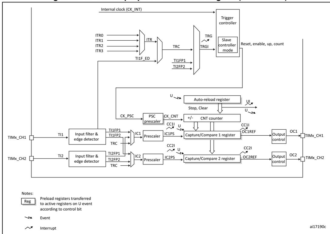
Figure 253. General-purpose timer block diagram (TIM9/TIM12)
24.2.2 TIM10/TIM11/TIM13/TIM14 main features
The features of general-purpose timers TIM10/TIM11/TIM13/TIM14 include:
- • 16-bit auto-reload upcounter
- • 16-bit programmable prescaler used to divide the counter clock frequency by any factor between 1 and 65536 (can be changed “on the fly”)
- • independent channel for:
- – Input capture
- – Output compare
- – PWM generation (edge-aligned mode)
- – One-pulse mode output
- • Interrupt generation on the following events:
- – Update: counter overflow, counter initialization (by software)
- – Input capture
- – Output compare
Figure 254. General-purpose timer block diagram (TIM10/TIM11/TIM13/TIM14)
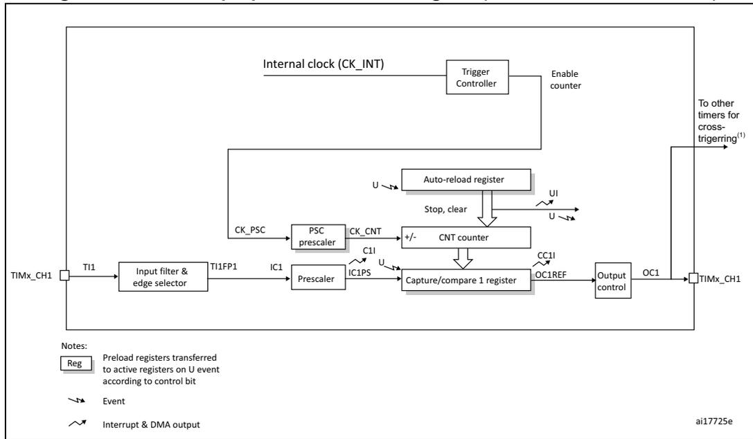
The diagram illustrates the internal architecture of a general-purpose timer. At the top, an 'Internal clock (CK_INT)' is connected to a 'Trigger Controller'. The 'Trigger Controller' outputs an 'Enable counter' signal to the 'CNT counter'. Below the counter is an 'Auto-reload register' which receives 'Stop, clear' and 'U' (update) signals. The 'CNT counter' is a '+/- CNT counter' that receives 'CK_PSC' from a 'PSC prescaler' and 'CK_CNT' from a 'Prescaler'. The 'Prescaler' also receives 'IC1' and 'IC1PS' signals. The 'CNT counter' is connected to a 'Capture/compare 1 register' which receives 'U' (update) and 'CC1' signals. This register outputs 'OC1REF' to an 'Output control' block, which in turn outputs 'OC1'. The 'OC1' signal is connected to 'TIMx_CH1' and also to 'To other timers for cross-triggering (1) '. The 'TIMx_CH1' input is connected to an 'Input filter & edge selector' which outputs 'TI1' and 'TI1FP1'. A legend at the bottom left defines symbols: 'Reg' for preload registers, a lightning bolt for 'Event', and a sawtooth for 'Interrupt & DMA output'. The identifier 'ai17725e' is in the bottom right corner.
- 1. This signal can be used as trigger for some slave timers, see Section 24.3.17: Using timer output as trigger for other timers (TIM10/TIM11/TIM13/TIM14) .
24.3 TIM9/TIM10/TIM11/TIM12/TIM13/TIM14 functional description
24.3.1 Time-base unit
The main block of the timer is a 16-bit up-counter with its related auto-reload register. The counter clock can be divided by a prescaler.
The counter, the auto-reload register and the prescaler register can be written or read by software. This is true even when the counter is running.
The time-base unit includes:
- • Counter register (TIMx_CNT)
- • Prescaler register (TIMx_PSC)
- • Auto-reload register (TIMx_ARR)
The auto-reload register is preloaded. Writing to or reading from the auto-reload register accesses the preload register. The content of the preload register are transferred into the shadow register permanently or at each update event (UEV), depending on the auto-reload preload enable bit (ARPE) in TIMx_CR1 register. The update event is sent when the counter reaches the overflow and if the UDIS bit equals 0 in the TIMx_CR1 register. It can also be generated by software. The generation of the update event is described in details for each configuration.
The counter is clocked by the prescaler output CK_CNT, which is enabled only when the counter enable bit (CEN) in TIMx_CR1 register is set (refer also to the slave mode controller description to get more details on counter enabling).
Note that the counter starts counting 1 clock cycle after setting the CEN bit in the TIMx_CR1 register.
Prescaler description
The prescaler can divide the counter clock frequency by any factor between 1 and 65536. It is based on a 16-bit counter controlled through a 16-bit register (in the TIMx_PSC register). It can be changed on the fly as this control register is buffered. The new prescaler ratio is taken into account at the next update event.
Figure 255 and Figure 256 give some examples of the counter behavior when the prescaler ratio is changed on the fly.
Figure 255. Counter timing diagram with prescaler division change from 1 to 2
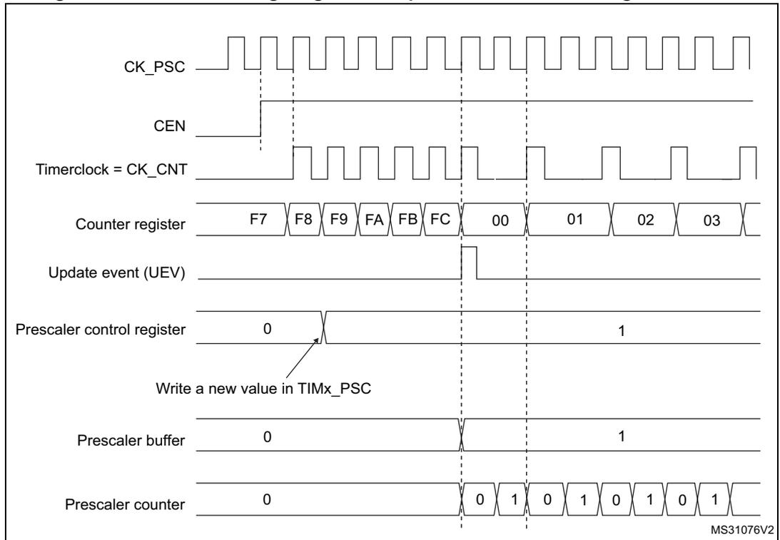
The diagram illustrates the timing of a general-purpose timer when the prescaler division is changed from 1 to 2. The top signal, CK_PSC, is a periodic clock. Below it, CEN (Counter Enable) is shown as a high-level signal. The Timerclock = CK_CNT is derived from CK_PSC. The Counter register shows a sequence of values: F7, F8, F9, FA, FB, FC, followed by 00, 01, 02, 03. An Update event (UEV) occurs when the counter reaches FC. The Prescaler control register is initially 0 and is changed to 1. A note indicates 'Write a new value in TIMx_PSC' pointing to the change in the control register. The Prescaler buffer initially shows 0 and changes to 1. The Prescaler counter counts from 0 to 1, then rolls over to 0, indicating a division of 2.
Figure 256. Counter timing diagram with prescaler division change from 1 to 4
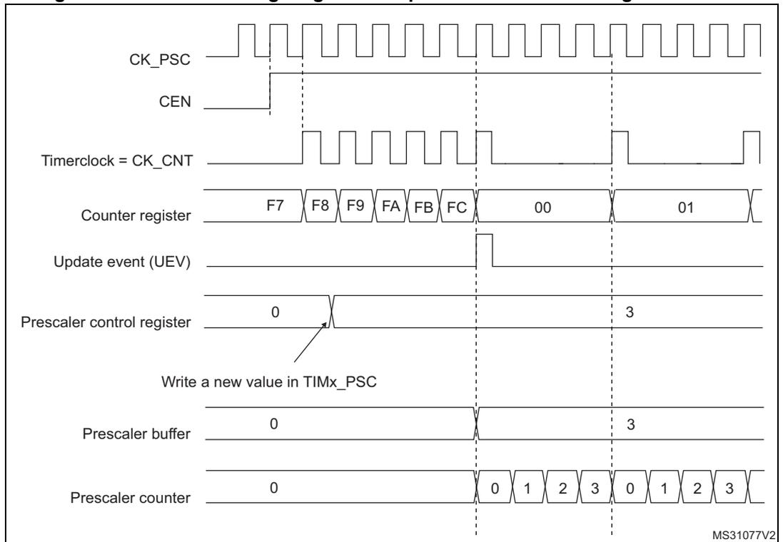
The diagram illustrates the timing of a general-purpose timer when the prescaler division is changed from 1 to 4. The top signal, CK_PSC, is a periodic clock. Below it, CEN (Counter Enable) is shown as a high-level signal. The Timerclock = CK_CNT is derived from CK_PSC. The Counter register shows a sequence of values: F7, F8, F9, FA, FB, FC, followed by 00, 01. An Update event (UEV) occurs when the counter reaches FC. The Prescaler control register is initially 0 and is changed to 3. A note indicates 'Write a new value in TIMx_PSC' pointing to the change in the control register. The Prescaler buffer initially shows 0 and changes to 3. The Prescaler counter counts from 0 to 3, then rolls over to 0, indicating a division of 4.
24.3.2 Counter modes
Upcounting mode
In upcounting mode, the counter counts from 0 to the auto-reload value (content of the TIMx_ARR register), then restarts from 0 and generates a counter overflow event.
Setting the UG bit in the TIMx_EGR register (by software or by using the slave mode controller on TIM9/TIM12) also generates an update event.
The UEV event can be disabled by software by setting the UDIS bit in the TIMx_CR1 register. This is to avoid updating the shadow registers while writing new values in the preload registers. Then no update event occurs until the UDIS bit has been written to 0. However, the counter restarts from 0, as well as the counter of the prescaler (but the prescale rate does not change). In addition, if the URS bit (update request selection) in TIMx_CR1 register is set, setting the UG bit generates an update event UEV but without setting the UIF flag (thus no interrupt is sent). This is to avoid generating both update and capture interrupts when clearing the counter on the capture event.
When an update event occurs, all the registers are updated and the update flag (UIF bit in TIMx_SR register) is set (depending on the URS bit):
- • The auto-reload shadow register is updated with the preload value (TIMx_ARR),
- • The buffer of the prescaler is reloaded with the preload value (content of the TIMx_PSC register).
The following figures show some examples of the counter behavior for different clock frequencies when TIMx_ARR=0x36.
Figure 257. Counter timing diagram, internal clock divided by 1
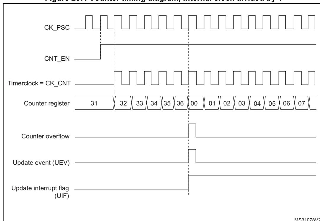
The timing diagram illustrates the counter's behavior in upcounting mode. The top signal, CK_PSC, is a periodic square wave. Below it, CNT_EN is a horizontal line that goes high to enable the counter. The third signal, Timerclock = CK_CNT, is a square wave that is active only when CNT_EN is high. The fourth signal shows the Counter register values: it starts at 31, increments through 32, 33, 34, 35, 36, then overflows to 00, 01, 02, 03, 04, 05, 06, and 07. The fifth signal, Counter overflow, is a pulse that goes high when the counter reaches 36 and returns low when it overflows to 00. The sixth signal, Update event (UEV), is a pulse that goes high at the overflow point. The bottom signal, Update interrupt flag (UIF), is a pulse that goes high at the overflow point and remains high until it is manually cleared. Vertical dashed lines indicate the timing relationships between the signals.
MS31078V2
Figure 258. Counter timing diagram, internal clock divided by 2
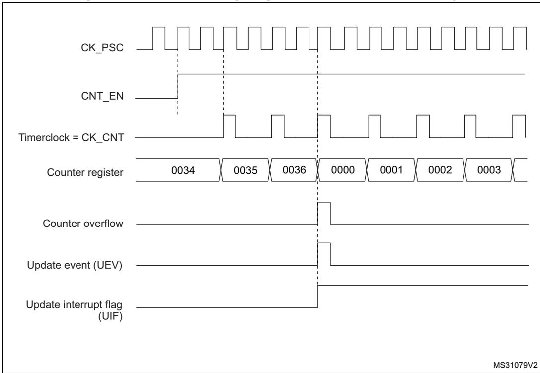
This timing diagram illustrates the operation of a general-purpose timer with the internal clock divided by 2. The top signal, CK_PSC, is a periodic square wave. Below it, CNT_EN is a horizontal line indicating the counter is enabled. The Timerclock (CK_CNT) is a square wave with a frequency half that of CK_PSC. The Counter register shows a sequence of values: 0034, 0035, 0036, 0000, 0001, 0002, and 0003. Vertical dashed lines mark the rising edges of the Timerclock. At the transition from 0036 to 0000, the Counter overflow signal pulses high. Simultaneously, the Update event (UEV) and the Update interrupt flag (UIF) also pulse high. The diagram is labeled MS31079V2 in the bottom right corner.
Figure 259. Counter timing diagram, internal clock divided by 4
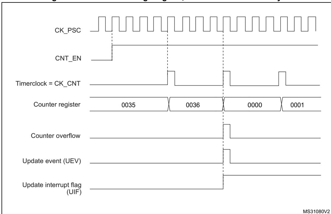
This timing diagram illustrates the operation of a general-purpose timer with the internal clock divided by 4. The top signal, CK_PSC, is a periodic square wave. Below it, CNT_EN is a horizontal line indicating the counter is enabled. The Timerclock (CK_CNT) is a square wave with a frequency one-quarter that of CK_PSC. The Counter register shows a sequence of values: 0035, 0036, 0000, and 0001. Vertical dashed lines mark the rising edges of the Timerclock. At the transition from 0036 to 0000, the Counter overflow signal pulses high. Simultaneously, the Update event (UEV) and the Update interrupt flag (UIF) also pulse high. The diagram is labeled MS31080V2 in the bottom right corner.
Figure 260. Counter timing diagram, internal clock divided by N
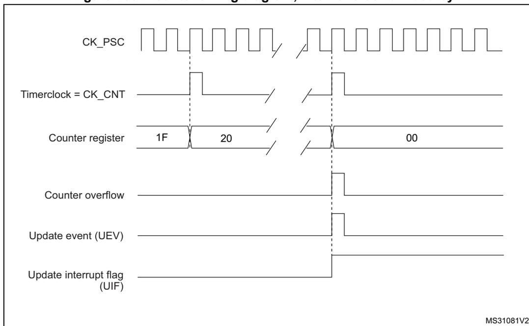
This timing diagram illustrates the relationship between several signals in a timer module when the internal clock is divided by N. The signals shown from top to bottom are:
- CK_PSC : The input clock to the prescaler, shown as a continuous square wave.
- Timerclock = CK_CNT : The clock signal after division, showing single pulses aligned with the rising edge of CK_PSC.
- Counter register : Shows the hexadecimal values of the counter. It transitions from 1F to 20, and later from a value (implied by a break) to 00.
- Counter overflow : A single high pulse that occurs when the counter register reaches its terminal value (00 in this case).
- Update event (UEV) : A single high pulse synchronized with the counter overflow.
- Update interrupt flag (UIF) : A signal that transitions from low to high at the moment of the update event.
The diagram includes break lines indicating a period of time has passed. The reference label is MS31081V2.
Figure 261. Counter timing diagram, update event when ARPE=0 (TIMx_ARR not preloaded)
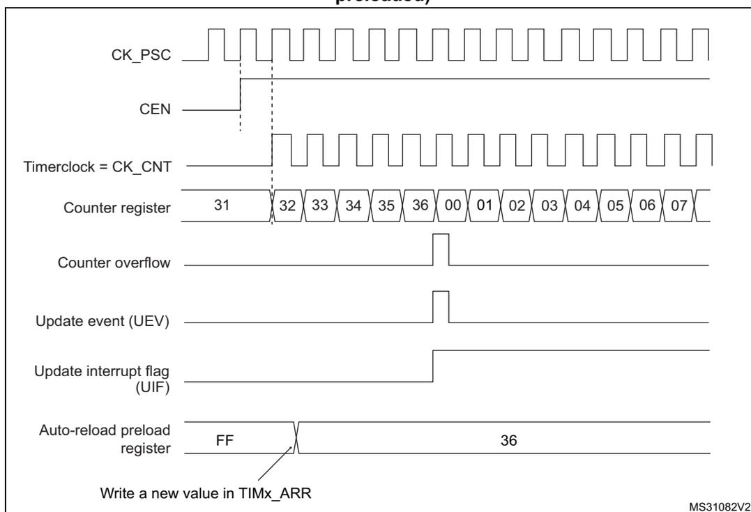
This timing diagram shows the behavior of the timer when the auto-reload preload is disabled (ARPE=0). The signals are:
- CK_PSC : The prescaler input clock (square wave).
- CEN : Counter enable signal, which goes high to start the timer.
- Timerclock = CK_CNT : The internal counter clock, which starts pulsing after CEN goes high.
- Counter register : Shows the counter incrementing: 31, 32, 33, 34, 35, 36, then resetting to 00 and continuing 01, 02, 03, 04, 05, 06, 07.
- Counter overflow : A pulse that occurs when the counter reaches the value 36.
- Update event (UEV) : A pulse synchronized with the overflow.
- Update interrupt flag (UIF) : Transitions high at the update event.
- Auto-reload preload register : Shows a value change from FF to 36. An arrow indicates "Write a new value in TIMx_ARR" occurs before the counter reaches 36.
Because ARPE=0, the new value (36) is taken into account immediately, causing the counter to overflow and reset to 00 once it reaches 36. The reference label is MS31082V2.
Figure 262. Counter timing diagram, update event when ARPE=1 (TIMx_ARR preloaded)
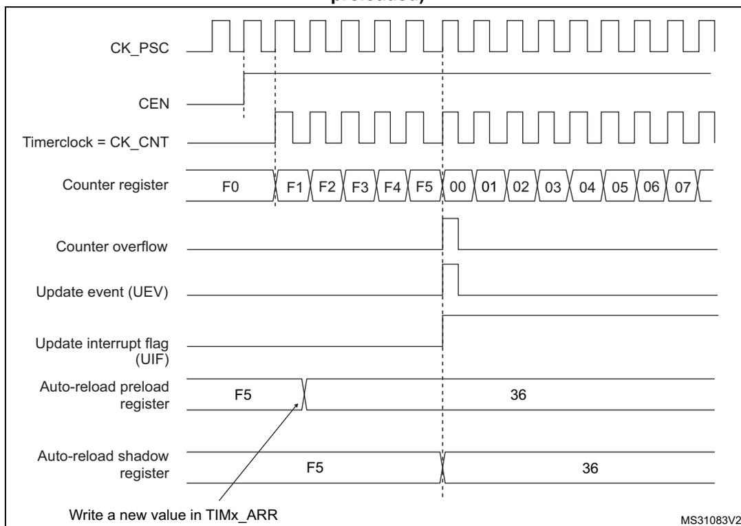
The timing diagram shows the following signals and registers over time:
- CK_PSC : Prescaler clock signal, shown as a square wave.
- CEN : Counter Enable signal, which goes high to enable the counter.
- Timerclock = CK_CNT : Counter clock signal, derived from CK_PSC.
- Counter register : Shows the counter values: F0, F1, F2, F3, F4, F5, 00, 01, 02, 03, 04, 05, 06, 07. The counter increments by 1 at each rising edge of the timer clock.
- Counter overflow : A pulse generated when the counter reaches the maximum value (00 after F5).
- Update event (UEV) : A pulse generated when the counter overflows.
- Update interrupt flag (UIF) : A pulse generated when the counter overflows.
- Auto-reload preload register : Shows the value F5 being written, then 36 being loaded into the register.
- Auto-reload shadow register : Shows the value F5 being loaded into the shadow register, then 36 being loaded into the shadow register.
- Write a new value in TIMx_ARR : An arrow indicates the time when a new value (F5) is written to the TIMx_ARR register.
MS31083V2
24.3.3 Clock selection
The counter clock can be provided by the following clock sources:
- • Internal clock (CK_INT)
- • External clock mode1 (for TIM9/TIM12): external input pin (TIx)
- • Internal trigger inputs (ITRx) (for TIM9/TIM12): connecting the trigger output from another timer. For instance, another timer can be configured as a prescaler for TIM12. Refer to Section : Using one timer as prescaler for another timer for more details.
Internal clock source (CK_INT)
The internal clock source is the default clock source for TIM10/TIM11/TIM13/TIM14.
For TIM9/TIM12, the internal clock source is selected when the slave mode controller is disabled (SMS='000'). The CEN bit in the TIMx_CR1 register and the UG bit in the TIMx_EGR register are then used as control bits and can be changed only by software (except for UG which remains cleared). As soon as the CEN bit is programmed to 1, the prescaler is clocked by the internal clock CK_INT.
Figure 263 shows the behavior of the control circuit and the upcounter in normal mode, without prescaler.
Figure 263. Control circuit in normal mode, internal clock divided by 1
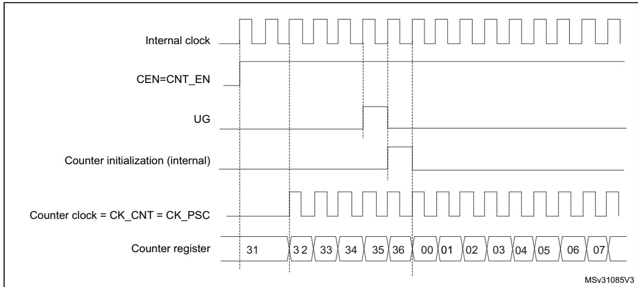
The timing diagram shows the following signals over time:
- Internal clock: A continuous square wave.
- CEN=CNT_EN: Counter Enable, which is initially high and then goes low.
- UG: Update Generation, which pulses high when CEN goes low.
- Counter initialization (internal): A pulse that occurs when UG goes high.
- Counter clock = CK_CNT = CK_PSC: The clock for the counter, which is the internal clock divided by 1.
- Counter register: Shows the count values: 31, 32, 33, 34, 35, 36, 00, 01, 02, 03, 04, 05, 06, 07. The count increments on each rising edge of the counter clock.
External clock source mode 1 (TIM9/TIM12)
This mode is selected when SMS='111' in the TIMx_SMCR register. The counter can count at each rising or falling edge on a selected input.
Figure 264. TI2 external clock connection example
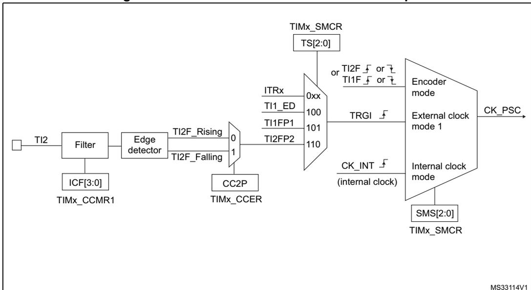
The block diagram illustrates the connection of the TI2 input to the external clock source mode 1. The TI2 input is connected to a Filter block, which is controlled by ICF[3:0] in the TIMx_CCMR1 register. The output of the Filter is connected to an Edge detector block, which generates TI2F_Rising and TI2F_Falling signals. These signals are connected to a multiplexer (MUX) controlled by CC2P in the TIMx_CCER register. The output of the MUX is connected to the TRGI input of the Encoder mode block. The Encoder mode block is controlled by TS[2:0] in the TIMx_SMCR register and SMS[2:0] in the TIMx_SMCR register. The TRGI input can also be selected from ITRx, TI1_ED, TI1FP1, or TI2FP2. The output of the Encoder mode block is the CK_PSC signal.
For example, to configure the upcounter to count in response to a rising edge on the TI2 input, use the following procedure:
- 1. Configure channel 2 to detect rising edges on the TI2 input by writing CC2S = '01' in the TIMx_CCMR1 register.
- 2. Configure the input filter duration by writing the IC2F[3:0] bits in the TIMx_CCMR1 register (if no filter is needed, keep IC2F='0000').
- 3. Select the rising edge polarity by writing CC2P='0' and CC2NP='0' in the TIMx_CCER register.
- 4. Configure the timer in external clock mode 1 by writing SMS='111' in the TIMx_SMCR register.
- 5. Select TI2 as the trigger input source by writing TS='110' in the TIMx_SMCR register.
- 6. Enable the counter by writing CEN='1' in the TIMx_CR1 register.
Note: The capture prescaler is not used for triggering, so it does not need to be configured.
When a rising edge occurs on TI2, the counter counts once and the TIF flag is set.
The delay between the rising edge on TI2 and the actual clock of the counter is due to the resynchronization circuit on TI2 input.
Figure 265. Control circuit in external clock mode 1
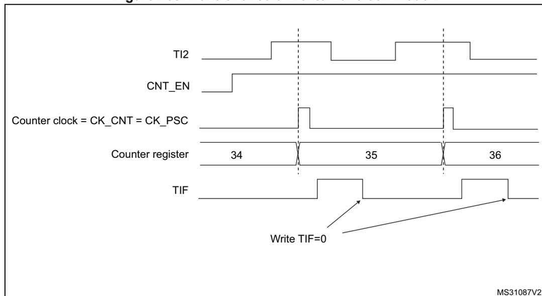
The diagram illustrates the timing for external clock mode 1. It shows five horizontal signal lines over time, separated by vertical dashed lines representing clock edges.
- TI2: The input signal shows two rising edges. The first rising edge occurs slightly after the first dashed line, and the second occurs slightly after the second dashed line.
- CNT_EN: This signal is shown as a single high level, indicating the counter is enabled throughout the sequence.
- Counter clock = CK_CNT = CK_PSC: This is a periodic square wave. Its rising edges are perfectly aligned with the vertical dashed lines, which correspond to the rising edges of the TI2 signal.
- Counter register: This line shows the value of the counter register. It starts at 34, remains constant until the first dashed line, then increments to 35 until the second dashed line, and finally increments to 36.
- TIF: The Timer Interrupt Flag. It is initially low. It goes high immediately after the first rising edge of TI2 (at the first dashed line) and returns to low when the value 'Write TIF=0' is indicated. It goes high again after the second rising edge of TI2 (at the second dashed line) and returns to low when 'Write TIF=0' is indicated again.
The diagram is labeled with 'MS31087V2' in the bottom right corner.
24.3.4 Capture/compare channels
Each Capture/Compare channel is built around a capture/compare register (including a shadow register), an input stage for capture (with digital filter, multiplexing and prescaler) and an output stage (with comparator and output control).
Figure 266 to Figure 268 give an overview of one capture/compare channel.
The input stage samples the corresponding TIx input to generate a filtered signal TIxF. Then, an edge detector with polarity selection generates a signal (TIxFPx) which can be used as trigger input by the slave mode controller or as the capture command. It is prescaled before the capture register (ICxPS).
Figure 266. Capture/compare channel (example: channel 1 input stage)
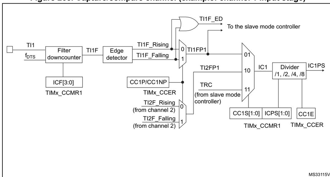
This diagram illustrates the input stage of a capture/compare channel. The input signal TI1 passes through a filter downcounter (controlled by ICF[3:0] from TIMx_CCMR1) to produce TI1F. This signal then enters an edge detector, which generates TI1F_Rising and TI1F_Falling signals. These signals are multiplexed with signals from channel 2 (TI2F_Rising, TI2F_Falling) and a TRC signal from the slave mode controller. The selected signal is captured by a divider (/1, /2, /4, /8) to produce IC1PS. Control signals for this stage include CC1P/CC1NP, TIMx_CCER, TI2FP1, CC1S[1:0], ICPS[1:0], and CC1E from TIMx_CCMR1. An OR gate combines TI1F_ED and TI1FP1 to signal the slave mode controller. The diagram is labeled MS33115V1.
The output stage generates an intermediate waveform which is then used for reference: OCxRef (active high). The polarity acts at the end of the chain.
Figure 267. Capture/compare channel 1 main circuit
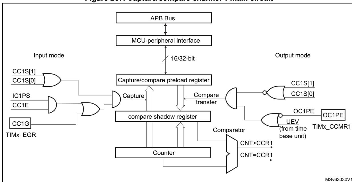
This diagram shows the main circuit of a capture/compare channel. It is divided into input and output modes. In input mode, signals CC1S[1], CC1S[0], IC1PS, CC1E, and CC1G (from TIMx_EGR) are processed through logic gates to control the capture into the capture/compare preload register. In output mode, the preload register feeds into a compare shadow register, which is then compared with the counter value (CNT) by a comparator. The comparator outputs CNT>CCR1 and CNT=CCR1. Control signals for output mode include CC1S[1], CC1S[0], OC1PE, and UEV (from the time base unit). The entire circuit is interfaced with an APB Bus via an MCU-peripheral interface, with a 16/32-bit data path. The diagram is labeled MSv63030V1.
Figure 268. Output stage of capture/compare channel (channel 1)
![Figure 268. Output stage of capture/compare channel (channel 1). The diagram shows the internal logic of the output stage. It starts with a counter (CNT) comparing with CCR1. The output mode controller takes CNT > CCR1 and CNT = CCR1 as inputs and produces OC1REF and OC2REF (on TIM12 only) signals. The output selector takes OC1REF, OC2REF, and a signal from the OC1M[3:0] bits in the TIMx_CCMR1 register. The selected signal is then passed through a multiplexer (0 or 1) controlled by CC1E in the TIM1_CCER register. The output of the multiplexer is inverted and then passed through another multiplexer (0 or 1) controlled by CC1P in the TIM1_CCER register. The output of this second multiplexer is then passed through an output enable circuit controlled by CC1E in the TIM1_CCER register to produce the final OC1 output. The diagram also shows connections to the master mode controller and a reference signal OC1REFC.](/RM0385-STM32F75-74/a352053ad2fec1739da5c965e3d10dc7_img.jpg)
1. Available on TIM12 only.
The capture/compare block is made of one preload register and one shadow register. Write and read always access the preload register.
In capture mode, captures are actually done in the shadow register, which is copied into the preload register.
In compare mode, the content of the preload register is copied into the shadow register which is compared to the counter.
24.3.5 Input capture mode
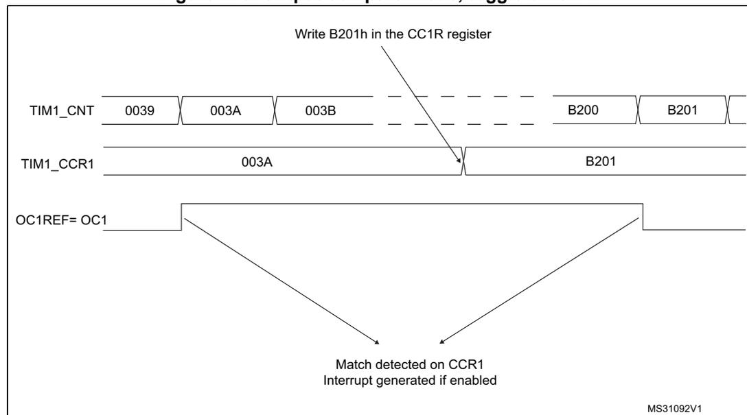
In Input capture mode, the Capture/Compare Registers (TIMx_CCRx) are used to latch the value of the counter after a transition detected by the corresponding ICx signal. When a capture occurs, the corresponding CCxIF flag (TIMx_SR register) is set and an interrupt or a DMA request can be sent if they are enabled. If a capture occurs while the CCxIF flag was already high, then the over-capture flag CCxOF (TIMx_SR register) is set. CCxIF can be cleared by software by writing it to '0' or by reading the captured data stored in the TIMx_CCRx register. CCxOF is cleared when it is written with 0.
The following example shows how to capture the counter value in TIMx_CCR1 when TI1 input rises. To do this, use the following procedure:
- 1. Select the active input: TIMx_CCR1 must be linked to the TI1 input, so write the CC1S bits to '01' in the TIMx_CCMR1 register. As soon as CC1S becomes different from '00', the channel is configured in input mode and the TIMx_CCR1 register becomes read-only.
- 2. Program the appropriate input filter duration in relation with the signal connected to the timer (by programming the ICxF bits in the TIMx_CCMRx register if the input is one of the TIx inputs). Let's imagine that, when toggling, the input signal is not stable during at most 5 internal clock cycles. We must program a filter duration longer than these 5 clock cycles. We can validate a transition on TI1 when 8 consecutive samples with the
new level have been detected (sampled at \( f_{DTS} \) frequency). Then write IC1F bits to '0011' in the TIMx_CCMR1 register.
- 3. Select the edge of the active transition on the TI1 channel by programming CC1P and CC1NP bits to '00' in the TIMx_CCER register (rising edge in this case).
- 4. Program the input prescaler. In our example, we wish the capture to be performed at each valid transition, so the prescaler is disabled (write IC1PS bits to '00' in the TIMx_CCMR1 register).
- 5. Enable capture from the counter into the capture register by setting the CC1E bit in the TIMx_CCER register.
- 6. If needed, enable the related interrupt request by setting the CC1IE bit in the TIMx_DIER register.
When an input capture occurs:
- • The TIMx_CCR1 register gets the value of the counter on the active transition.
- • CC1IF flag is set (interrupt flag). CC1OF is also set if at least two consecutive captures occurred whereas the flag was not cleared.
- • An interrupt is generated depending on the CC1IE bit.
In order to handle the overcapture, it is recommended to read the data before the overcapture flag. This is to avoid missing an overcapture which could happen after reading the flag and before reading the data.
Note: IC interrupt requests can be generated by software by setting the corresponding CCxG bit in the TIMx_EGR register.
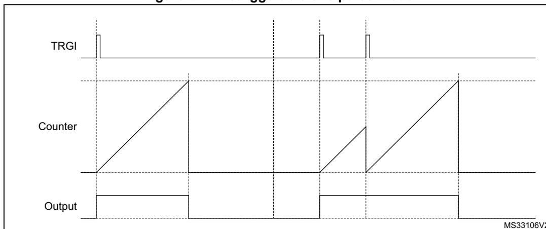
24.3.6 PWM input mode (only for TIM9/TIM12)
This mode is a particular case of input capture mode. The procedure is the same except:
- • Two ICx signals are mapped on the same Tlx input.
- • These 2 ICx signals are active on edges with opposite polarity.
- • One of the two TlxFP signals is selected as trigger input and the slave mode controller is configured in reset mode.
For example, one can measure the period (in TIMx_CCR1 register) and the duty cycle (in TIMx_CCR2 register) of the PWM applied on TI1 using the following procedure (depending on CK_INT frequency and prescaler value):
- 1. Select the active input for TIMx_CCR1: write the CC1S bits to '01' in the TIMx_CCMR1 register (TI1 selected).
- 2. Select the active polarity for TI1FP1 (used both for capture in TIMx_CCR1 and counter clear): program the CC1P and CC1NP bits to '00' (active on rising edge).
- 3. Select the active input for TIMx_CCR2: write the CC2S bits to '10' in the TIMx_CCMR1 register (TI1 selected).
- 4. Select the active polarity for TI1FP2 (used for capture in TIMx_CCR2): program the CC2P and CC2NP bits to '10' (active on falling edge).
- 5. Select the valid trigger input: write the TS bits to '101' in the TIMx_SMCR register (TI1FP1 selected).
- 6. Configure the slave mode controller in reset mode: write the SMS bits to '100' in the TIMx_SMCR register.
- 7. Enable the captures: write the CC1E and CC2E bits to '1' in the TIMx_CCER register.
Figure 269. PWM input mode timing
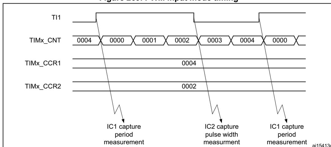
- 1. The PWM input mode can be used only with the TIMx_CH1/TIMx_CH2 signals due to the fact that only TI1FP1 and TI2FP2 are connected to the slave mode controller.
24.3.7 Forced output mode
In output mode (CCxS bits = '00' in the TIMx_CCMRx register), each output compare signal (OCxREF and then OCx) can be forced to active or inactive level directly by software, independently of any comparison between the output compare register and the counter.
To force an output compare signal (OCXREF/OCx) to its active level, one just needs to write '0101' in the OCxM bits in the corresponding TIMx_CCMRx register. Thus OCXREF is forced high (OCxREF is always active high) and OCx get opposite value to CCxP polarity bit.
For example: CCxP='0' (OCx active high) => OCx is forced to high level.
The OCxREF signal can be forced low by writing the OCxM bits to '0100' in the TIMx_CCMRx register.
Anyway, the comparison between the TIMx_CCRx shadow register and the counter is still performed and allows the flag to be set. Interrupt requests can be sent accordingly. This is described in the output compare mode section below.
24.3.8 Output compare mode
This function is used to control an output waveform or indicating when a period of time has elapsed.
When a match is found between the capture/compare register and the counter, the output compare function:
- 1. Assigns the corresponding output pin to a programmable value defined by the output compare mode (OCxM bits in the TIMx_CCMRx register) and the output polarity (CCxP bit in the TIMx_CCER register). The output pin can keep its level (OCxM='0000'), be set active (OCxM='0001'), be set inactive (OCxM='0010') or can toggle (OCxM='0011') on match.
- 2. Sets a flag in the interrupt status register (CCxIF bit in the TIMx_SR register).
- 3. Generates an interrupt if the corresponding interrupt mask is set (CCXIE bit in the TIMx_DIER register).
The TIMx_CCRx registers can be programmed with or without preload registers using the OCxPE bit in the TIMx_CCMRx register.
In output compare mode, the update event UEV has no effect on OCxREF and OCx output. The timing resolution is one count of the counter. Output compare mode can also be used to output a single pulse (in One-pulse mode).
Procedure:
- 1. Select the counter clock (internal, external, prescaler).
- 2. Write the desired data in the TIMx_ARR and TIMx_CCRx registers.
- 3. Set the CCxIE bit if an interrupt request is to be generated.
- 4. Select the output mode. For example:
- – Write OCxM = '0011' to toggle OCx output pin when CNT matches CCRx
- – Write OCxPE = '0' to disable preload register
- – Write CCxP = '0' to select active high polarity
- – Write CCxE = '1' to enable the output
- 5. Enable the counter by setting the CEN bit in the TIMx_CR1 register.
The TIMx_CCRx register can be updated at any time by software to control the output waveform, provided that the preload register is not enabled (OCxPE='0', else TIMx_CCRx shadow register is updated only at the next update event UEV). An example is given in Figure 270 .
Figure 270. Output compare mode, toggle on OC1.
24.3.9 PWM mode
Pulse Width Modulation mode allows to generate a signal with a frequency determined by the value of the TIMx_ARR register and a duty cycle determined by the value of the TIMx_CCRx register.
The PWM mode can be selected independently on each channel (one PWM per OCx output) by writing '0110' (PWM mode 1) or '0111' (PWM mode 2) in the OCxM bits in the
TIMx_CCMRx register. The corresponding preload register must be enabled by setting the OCxPE bit in the TIMx_CCMRx register, and eventually the auto-reload preload register (in upcounting or center-aligned modes) by setting the ARPE bit in the TIMx_CR1 register.
As the preload registers are transferred to the shadow registers only when an update event occurs, before starting the counter, all registers must be initialized by setting the UG bit in the TIMx_EGR register.
The OCx polarity is software programmable using the CCxP bit in the TIMx_CCER register. It can be programmed as active high or active low. The OCx output is enabled by the CCxE bit in the TIMx_CCER register. Refer to the TIMx_CCERx register description for more details.
In PWM mode (1 or 2), TIMx_CNT and TIMx_CCRx are always compared to determine whether \( TIMx\_CNT \leq TIMx\_CCRx \) .
The timer is able to generate PWM in edge-aligned mode only since the counter is upcounting.
In the following example, we consider PWM mode 1. The reference PWM signal OCxREF is high as long as \( TIMx\_CNT < TIMx\_CCRx \) else it becomes low. If the compare value in TIMx_CCRx is greater than the auto-reload value (in TIMx_ARR) then OCxREF is held at '1'. If the compare value is 0 then OCxRef is held at '0'. Figure 271 shows some edge-aligned PWM waveforms in an example where TIMx_ARR=8.
Figure 271. Edge-aligned PWM waveforms (ARR=8)
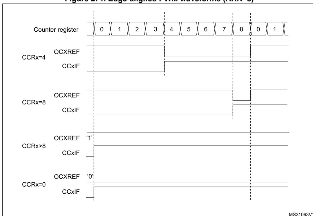
The diagram illustrates the relationship between the Counter register (values 0 to 8, then repeating 0 to 1) and the resulting PWM signals (OCxREF and CCxIF) for four different CCRx settings. Vertical dashed lines mark the counter values 0, 4, 8, and 0 (next cycle).
- CCRx=4: OCxREF is high from counter 0 to 3, and low from 4 to 8. CCxIF pulses high at counter 4.
- CCRx=8: OCxREF is high from counter 0 to 7, and low at counter 8. CCxIF pulses high at counter 8.
- CCRx>8: OCxREF remains high throughout the entire cycle (0 to 8). CCxIF is not shown as it would not pulse within this cycle.
- CCRx=0: OCxREF is held low throughout the entire cycle (0 to 8). CCxIF pulses high at counter 0.
MS31093V1
24.3.10 Combined PWM mode (TIM9/TIM12 only)
Combined PWM mode allows two edge or center-aligned PWM signals to be generated with programmable delay and phase shift between respective pulses. While the frequency is determined by the value of the TIMx_ARR register, the duty cycle and delay are determined
by the two TIMx_CCRx registers. The resulting signals, OCxREFC, are made of an OR or AND logical combination of two reference PWMs:
- • OC1REFC (or OC2REFC) is controlled by the TIMx_CCR1 and TIMx_CCR2 registers
Combined PWM mode can be selected independently on two channels (one OCx output per pair of CCR registers) by writing '1100' (Combined PWM mode 1) or '1101' (Combined PWM mode 2) in the OCxM bits in the TIMx_CCMRx register.
When a given channel is used as a combined PWM channel, its complementary channel must be configured in the opposite PWM mode (for instance, one in Combined PWM mode 1 and the other in Combined PWM mode 2).
Note: The OCxM[3:0] bit field is split into two parts for compatibility reasons, the most significant bit is not contiguous with the 3 least significant ones.
Figure 272 represents an example of signals that can be generated using combined PWM mode, obtained with the following configuration:
- • Channel 1 is configured in Combined PWM mode 2,
- • Channel 2 is configured in PWM mode 1,
Figure 272. Combined PWM mode on channel 1 and 2
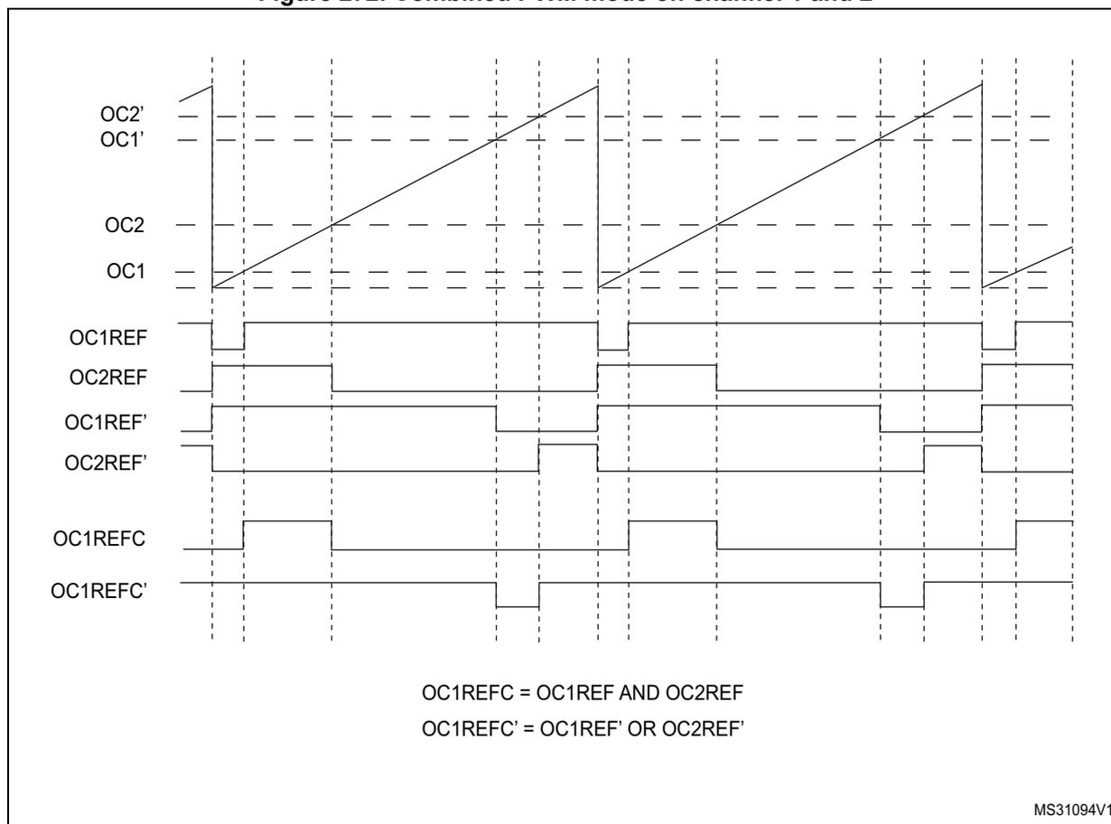
OC1REFC = OC1REF AND OC2REF
OC1REFC' = OC1REF' OR OC2REF'
MS31094V1
24.3.11 One-pulse mode
One-pulse mode (OPM) is a particular case of the previous modes. It allows the counter to be started in response to a stimulus and to generate a pulse with a programmable length after a programmable delay.
Starting the counter can be controlled through the slave mode controller. Generating the waveform can be done in output compare mode or PWM mode. One-pulse mode is selected by setting the OPM bit in the TIMx_CR1 register. This makes the counter stop automatically at the next update event UEV.
A pulse can be correctly generated only if the compare value is different from the counter initial value. Before starting (when the timer is waiting for the trigger), the configuration must be as follows:
Figure 273. Example of one pulse mode.
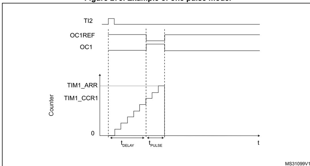
The diagram illustrates the timing for one-pulse mode. The top signal, TI2, shows a single rising edge that triggers the counter. Below it, OC1REF and OC1 show the output signals. OC1REF is initially high and goes low when the counter starts. OC1 is initially low and goes high when the counter starts. The bottom graph shows the Counter value over time. The counter starts at 0 and increments in a staircase fashion until it reaches the TIM1_ARR value, at which point it stops. The time interval between the rising edge of TI2 and the start of the counter is labeled t_DELAY. The time interval between the start of the counter and the point where it reaches TIM1_ARR is labeled t_PULSE. The diagram is labeled MS31099V1 in the bottom right corner.
For example one may want to generate a positive pulse on OC1 with a length of \( t_{\text{PULSE}} \) and after a delay of \( t_{\text{DELAY}} \) as soon as a positive edge is detected on the TI2 input pin.
Use TI2FP2 as trigger 1:
- 1. Map TI2FP2 to TI2 by writing CC2S='01' in the TIMx_CCMR1 register.
- 2. TI2FP2 must detect a rising edge, write CC2P='0' and CC2NP='0' in the TIMx_CCER register.
- 3. Configure TI2FP2 as trigger for the slave mode controller (TRGI) by writing TS='110' in the TIMx_SMCR register.
- 4. TI2FP2 is used to start the counter by writing SMS to '110' in the TIMx_SMCR register (trigger mode).
The OPM waveform is defined by writing the compare registers (taking into account the clock frequency and the counter prescaler).
- • The \( t_{\text{DELAY}} \) is defined by the value written in the TIMx_CCR1 register.
- • The \( t_{\text{PULSE}} \) is defined by the difference between the auto-reload value and the compare value (TIMx_ARR - TIMx_CCR1).
- • Let's say one want to build a waveform with a transition from '0' to '1' when a compare match occurs and a transition from '1' to '0' when the counter reaches the auto-reload value. To do this PWM mode 2 must be enabled by writing OC1M='0111' in the TIMx_CCMR1 register. Optionally the preload registers can be enabled by writing OC1PE='1' in the TIMx_CCMR1 register and ARPE in the TIMx_CR1 register. In this case one has to write the compare value in the TIMx_CCR1 register, the auto-reload value in the TIMx_ARR register, generate an update by setting the UG bit and wait for external trigger event on TI2. CC1P is written to '0' in this example.
Since only 1 pulse (Single mode) is needed, a 1 must be written in the OPM bit in the TIMx_CR1 register to stop the counter at the next update event (when the counter rolls over from the auto-reload value back to 0). When OPM bit in the TIMx_CR1 register is set to '0', so the Repetitive Mode is selected.
Particular case: OCx fast enable
In One-pulse mode, the edge detection on TIx input set the CEN bit which enables the counter. Then the comparison between the counter and the compare value makes the output toggle. But several clock cycles are needed for these operations and it limits the minimum delay \( t_{\text{DELAY}} \) min we can get.
If one wants to output a waveform with the minimum delay, the OCxFE bit can be set in the TIMx_CCMRx register. Then OCxRef (and OCx) are forced in response to the stimulus, without taking in account the comparison. Its new level is the same as if a compare match had occurred. OCxFE acts only if the channel is configured in PWM1 or PWM2 mode.
24.3.12 Retriggerable one pulse mode (TIM12 only)
This mode allows the counter to be started in response to a stimulus and to generate a pulse with a programmable length, but with the following differences with non-retriggerable one pulse mode described in Section 24.3.11: One-pulse mode :
- • The pulse starts as soon as the trigger occurs (no programmable delay)
- • The pulse is extended if a new trigger occurs before the previous one is completed
The timer must be in Slave mode, with the bits SMS[3:0] = '1000' (Combined Reset + trigger mode) in the TIMx_SMCR register, and the OCxM[3:0] bits set to '1000' or '1001' for retriggerable OPM mode 1 or 2.
If the timer is configured in up-counting mode, the corresponding CCRx must be set to 0 (the ARR register sets the pulse length). If the timer is configured in down-counting mode, CCRx must be above or equal to ARR.
Note: The OCxM[3:0] and SMS[3:0] bit fields are split into two parts for compatibility reasons, the most significant bit are not contiguous with the 3 least significant ones.
This mode must not be used with center-aligned PWM modes. It is mandatory to have CMS[1:0] = 00 in TIMx_CR1.
Figure 274. Retriggerable one pulse mode
24.3.13 UIF bit remapping
The IUFREMAP bit in the TIMx_CR1 register forces a continuous copy of the Update Interrupt Flag UIF into bit 31 of the timer counter register (TIMxCNT[31]). This allows to atomically read both the counter value and a potential roll-over condition signaled by the UIFCPY flag. In particular cases, it can ease the calculations by avoiding race conditions caused for instance by a processing shared between a background task (counter reading) and an interrupt (Update Interrupt).
There is no latency between the assertions of the UIF and UIFCPY flags.
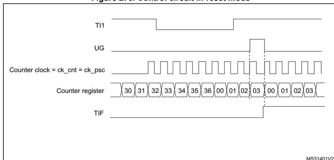
24.3.14 TIM9/TIM12 external trigger synchronization
The TIM9/TIM12 timers can be synchronized with an external trigger in several modes: Reset mode, Gated mode and Trigger mode.
Slave mode: Reset mode
The counter and its prescaler can be reinitialized in response to an event on a trigger input. Moreover, if the URS bit from the TIMx_CR1 register is low, an update event UEV is generated. Then all the preloaded registers (TIMx_ARR, TIMx_CCRx) are updated.
In the following example, the upcounter is cleared in response to a rising edge on TI1 input:
- 1. Configure the channel 1 to detect rising edges on TI1. Configure the input filter duration (in this example, we do not need any filter, so we keep IC1F='0000'). The capture prescaler is not used for triggering, so it does not need to be configured. The CC1S bits select the input capture source only, CC1S = '01' in the TIMx_CCMR1 register. Program CC1P and CC1NP to '00' in TIMx_CCER register to validate the polarity (and detect rising edges only).
- 2. Configure the timer in reset mode by writing SMS='100' in TIMx_SMCR register. Select TI1 as the input source by writing TS='101' in TIMx_SMCR register.
- 3. Start the counter by writing CEN='1' in the TIMx_CR1 register.
The counter starts counting on the internal clock, then behaves normally until TI1 rising edge. When TI1 rises, the counter is cleared and restarts from 0. In the meantime, the trigger flag is set (TIF bit in the TIMx_SR register) and an interrupt request can be sent if enabled (depending on the TIE bit in TIMx_DIER register).
The following figure shows this behavior when the auto-reload register TIMx_ARR=0x36. The delay between the rising edge on TI1 and the actual reset of the counter is due to the resynchronization circuit on TI1 input.
Figure 275. Control circuit in reset mode
Slave mode: Gated mode
The counter can be enabled depending on the level of a selected input.
In the following example, the upcounter counts only when TI1 input is low:
- 1. Configure the channel 1 to detect low levels on TI1. Configure the input filter duration (in this example, we do not need any filter, so we keep IC1F='0000'). The capture prescaler is not used for triggering, so it does not need to be configured. The CC1S bits select the input capture source only, CC1S='01' in TIMx_CCMR1 register. Program CC1P='1' and CC1NP='0' in TIMx_CCER register to validate the polarity (and detect low level only).
- 2. Configure the timer in gated mode by writing SMS='101' in TIMx_SMCR register. Select TI1 as the input source by writing TS='101' in TIMx_SMCR register.
- 3. Enable the counter by writing CEN='1' in the TIMx_CR1 register (in gated mode, the counter doesn't start if CEN='0', whatever is the trigger input level).
The counter starts counting on the internal clock as long as TI1 is low and stops as soon as TI1 becomes high. The TIF flag in the TIMx_SR register is set both when the counter starts or stops.
The delay between the rising edge on TI1 and the actual stop of the counter is due to the resynchronization circuit on TI1 input.
Figure 276. Control circuit in gated mode
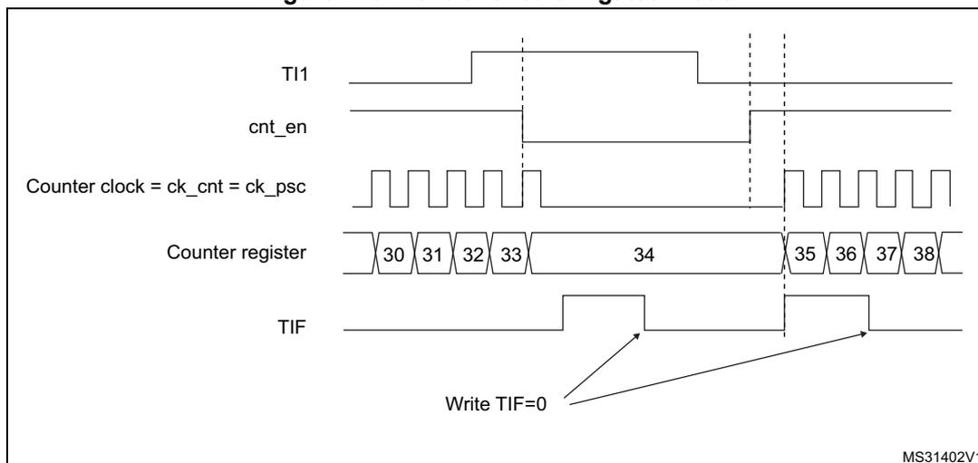
MS31402V1
Slave mode: Trigger mode
The counter can start in response to an event on a selected input.
In the following example, the upcounter starts in response to a rising edge on TI2 input:
- 1. Configure the channel 2 to detect rising edges on TI2. Configure the input filter duration (in this example, we do not need any filter, so we keep IC2F='0000'). The capture prescaler is not used for triggering, so it does not need to be configured. The CC2S bits are configured to select the input capture source only, CC2S='01' in TIMx_CCMR1 register. Program CC2P='1' and CC2NP='0' in TIMx_CCER register to validate the polarity (and detect low level only).
- 2. Configure the timer in trigger mode by writing SMS='110' in TIMx_SMCR register. Select TI2 as the input source by writing TS='110' in TIMx_SMCR register.
When a rising edge occurs on TI2, the counter starts counting on the internal clock and the TIF flag is set.
The delay between the rising edge on TI2 and the actual start of the counter is due to the resynchronization circuit on TI2 input.
Figure 277. Control circuit in trigger mode
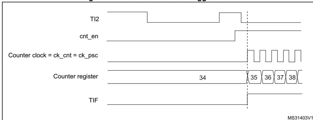
MS31403V1
24.3.15 Slave mode – combined reset + trigger modeIn this case, a rising edge of the selected trigger input (TRGI) reinitializes the counter, generates an update of the registers, and starts the counter.
This mode is used for one-pulse mode.
24.3.16 Timer synchronization (TIM9/TIM12)
The TIM timers are linked together internally for timer synchronization or chaining. Refer to Section 23.3.19: Timer synchronization for details.
Note: The clock of the slave timer must be enabled prior to receive events from the master timer, and must not be changed on-the-fly while triggers are received from the master timer.
24.3.17 Using timer output as trigger for other timers (TIM10/TIM11/TIM13/TIM14)
The timers with one channel only do not feature a master mode. However, the OC1 output signal can be used to trigger some other timers (including timers described in other sections of this document). Check the “TIMx internal trigger connection” table of any TIMx_SMCR register on the device to identify which timers can be targeted as slave.
The OC1 signal pulse width must be programmed to be at least 2 clock cycles of the destination timer, to make sure the slave timer will detect the trigger.
For instance, if the destination's timer CK_INT clock is 4 times slower than the source timer, the OC1 pulse width must be 8 clock cycles.
24.3.18 Debug mode
When the microcontroller enters debug mode (Cortex®-M7 core halted), the TIMx counter either continues to work normally or stops, depending on DBG_TIMx_STOP configuration bit in DBG module. For more details, refer to Section 40.16.2: Debug support for timers, watchdog, bxCAN and I 2 C .
24.4 TIM9/TIM12 registers
Refer to Section 1.2 for a list of abbreviations used in register descriptions.
The peripheral registers have to be written by half-words (16 bits) or words (32 bits). Read accesses can be done by bytes (8 bits), half-words (16 bits) or words (32 bits).
24.4.1 TIMx control register 1 (TIMx_CR1)(x = 9, 12)
Address offset: 0x00
Reset value: 0x0000
| 15 | 14 | 13 | 12 | 11 | 10 | 9 | 8 | 7 | 6 | 5 | 4 | 3 | 2 | 1 | 0 |
|---|---|---|---|---|---|---|---|---|---|---|---|---|---|---|---|
| Res. | Res. | Res. | Res. | UIFREMAP | Res. | CKD[1:0] | ARPE | Res. | Res. | Res. | OPM | URS | UDIS | CEN | |
| rw | rw | rw | rw | rw | rw | rw | |||||||||
Bits 15:12 Reserved, must be kept at reset value.
Bit 11 UIFREMAP : UIF status bit remapping
0: No remapping. UIF status bit is not copied to TIMx_CNT register bit 31.
1: Remapping enabled. UIF status bit is copied to TIMx_CNT register bit 31.
Bit 10 Reserved, must be kept at reset value.
Bits 9:8 CKD[1:0] : Clock division
This bit-field indicates the division ratio between the timer clock (CK_INT) frequency and sampling clock used by the digital filters (TIx),
00: \( t_{DTS} = t_{CK\_INT} \)
01: \( t_{DTS} = 2 \times t_{CK\_INT} \)
10: \( t_{DTS} = 4 \times t_{CK\_INT} \)
11: Reserved
Bit 7 ARPE : Auto-reload preload enable
0: TIMx_ARR register is not buffered.
1: TIMx_ARR register is buffered.
Bits 6:4 Reserved, must be kept at reset value.
Bit 3 OPM : One-pulse mode
0: Counter is not stopped on the update event
1: Counter stops counting on the next update event (clearing the CEN bit).
Bit 2 URS : Update request source
This bit is set and cleared by software to select the UEV event sources.
0: Any of the following events generates an update interrupt if enabled. These events can be:
- – Counter overflow
- – Setting the UG bit
- – Update generation through the slave mode controller
1: Only counter overflow generates an update interrupt if enabled.
Bit 1 UDIS : Update disable
This bit is set and cleared by software to enable/disable update event (UEV) generation.
0: UEV enabled. An UEV is generated by one of the following events:
- – Counter overflow
- – Setting the UG bit
Buffered registers are then loaded with their preload values.
1: UEV disabled. No UEV is generated, shadow registers keep their value (ARR, PSC, CCRx). The counter and the prescaler are reinitialized if the UG bit is set.
Bit 0 CEN : Counter enable
0: Counter disabled
1: Counter enabled
CEN is cleared automatically in one-pulse mode, when an update event occurs.
Note: External clock and gated mode can work only if the CEN bit has been previously set by software. However trigger mode can set the CEN bit automatically by hardware.
24.4.2 TIMx slave mode control register (TIMx_SMCR)(x = 9, 12)
Address offset: 0x08
Reset value: 0x0000 0000
| 31 | 30 | 29 | 28 | 27 | 26 | 25 | 24 | 23 | 22 | 21 | 20 | 19 | 18 | 17 | 16 |
|---|---|---|---|---|---|---|---|---|---|---|---|---|---|---|---|
| Res. | Res. | Res. | Res. | Res. | Res. | Res. | Res. | Res. | Res. | Res. | Res. | Res. | Res. | Res. | SMS[3] |
| rw | |||||||||||||||
| 15 | 14 | 13 | 12 | 11 | 10 | 9 | 8 | 7 | 6 | 5 | 4 | 3 | 2 | 1 | 0 |
| Res. | Res. | Res. | Res. | Res. | Res. | Res. | Res. | MSM | TS[2:0] | Res. | SMS[2:0] | ||||
| rw | rw | rw | rw | rw | rw | rw | |||||||||
Bits 31:17 Reserved, must be kept at reset value.
Bits 15:8 Reserved, must be kept at reset value.
Bit 7 MSM : Master/Slave mode
0: No action
1: The effect of an event on the trigger input (TRGI) is delayed to allow a perfect synchronization between the current timer and its slaves (through TRGO). It is useful in order to synchronize several timers on a single external event.
Bits 6:4 TS[2:0] : Trigger selection
This bitfield selects the trigger input to be used to synchronize the counter.
000: Internal Trigger 0 (ITR0)
001: Internal Trigger 1 (ITR1)
010: Internal Trigger 2 (ITR2)
011: Internal Trigger 3 (ITR3)
100: TI1 Edge Detector (TI1F_ED)
101: Filtered Timer Input 1 (TI1FP1)
110: Filtered Timer Input 2 (TI2FP2)
111: Reserved.
See Table 157: TIMx internal trigger connection on page 830 for more details on the meaning of ITRx for each timer.
Note: These bits must be changed only when they are not used (e.g. when SMS='000') to avoid wrong edge detections at the transition.
Bit 3 Reserved, must be kept at reset value.
Bits 16, 2, 1, 0 SMS[3:0] : Slave mode selection
When external signals are selected the active edge of the trigger signal (TRGI) is linked to the polarity selected on the external input (refer to ETP bit in TIMx_SMCR for tim_etr_in and CCxP/CCxNP bits in TIMx_CCER register for tim_ti1fp1 and tim_ti2fp2).
0000: Slave mode disabled - if CEN = '1' then the prescaler is clocked directly by the internal clock.
0001: Reserved
0010: Reserved
0011: Reserved
0100: Reset Mode - Rising edge of the selected trigger input (TRGI) reinitializes the counter and generates an update of the registers.
0101: Gated Mode - The counter clock is enabled when the trigger input (TRGI) is high. The counter stops (but is not reset) as soon as the trigger becomes low. Both start and stop of the counter are controlled.
0110: Trigger Mode - The counter starts at a rising edge of the trigger TRGI (but it is not reset). Only the start of the counter is controlled.
0111: External Clock Mode 1 - Rising edges of the selected trigger (TRGI) clock the counter.
1000: Combined reset + trigger mode - Rising edge of the selected trigger input (TRGI) reinitializes the counter, generates an update of the registers and starts the counter.
Other codes: reserved.
Note: The gated mode must not be used if TI1F_ED is selected as the trigger input (TS='100'). Indeed, TI1F_ED outputs 1 pulse for each transition on TI1F, whereas the gated mode checks the level of the trigger signal.
Note: The clock of the slave timer must be enabled prior to receive events from the master timer, and must not be changed on-the-fly while triggers are received from the master timer.
Table 157. TIMx internal trigger connection
| Slave TIM | ITR0 (TS = '000') | ITR1 (TS = '001') | ITR2 (TS = '010') | ITR3 (TS = '011') |
|---|---|---|---|---|
| TIM9 | TIM2 | TIM3 | TIM10_OC | TIM11_OC |
| TIM12 | TIM4 | TIM5 | TIM13_OC | TIM14_OC |
24.4.3 TIMx Interrupt enable register (TIMx_DIER)(x = 9, 12)
Address offset: 0x0C
Reset value: 0x0000
| 15 | 14 | 13 | 12 | 11 | 10 | 9 | 8 | 7 | 6 | 5 | 4 | 3 | 2 | 1 | 0 |
|---|---|---|---|---|---|---|---|---|---|---|---|---|---|---|---|
| Res. | Res. | Res. | Res. | Res. | Res. | Res. | Res. | Res. | TIE | Res. | Res. | Res. | CC2IE | CC1IE | UIE |
| rw | rw | rw | rw |
Bits 15:7 Reserved, must be kept at reset value.
Bit 6 TIE : Trigger interrupt enable
0: Trigger interrupt disabled.
1: Trigger interrupt enabled.
Bits 5:3 Reserved, must be kept at reset value.
Bit 2 CC2IE : Capture/Compare 2 interrupt enable
0: CC2 interrupt disabled.
1: CC2 interrupt enabled.
Bit 1 CC1IE : Capture/Compare 1 interrupt enable
0: CC1 interrupt disabled.
1: CC1 interrupt enabled.
Bit 0 UIE : Update interrupt enable
0: Update interrupt disabled.
1: Update interrupt enabled.
24.4.4 TIMx status register (TIMx_SR)(x = 9, 12)
Address offset: 0x10
Reset value: 0x0000
| 15 | 14 | 13 | 12 | 11 | 10 | 9 | 8 | 7 | 6 | 5 | 4 | 3 | 2 | 1 | 0 |
|---|---|---|---|---|---|---|---|---|---|---|---|---|---|---|---|
| Res. | Res. | Res. | Res. | Res. | CC2OF | CC1OF | Res. | Res. | TIF | Res. | Res. | Res. | CC2IF | CC1IF | UIF |
| rc_w0 | rc_w0 | rc_w0 | rc_w0 | rc_w0 | rc_w0 |
Bits 15:11 Reserved, must be kept at reset value.
Bit 10
CC2OF
: Capture/compare 2 overcapture flag
refer to CC1OF description
Bit 9 CC1OF : Capture/Compare 1 overcapture flag
This flag is set by hardware only when the corresponding channel is configured in input capture mode. It is cleared by software by writing it to '0'.
0: No overcapture has been detected.
1: The counter value has been captured in TIMx_CCR1 register while CC1IF flag was already set
Bits 8:7 Reserved, must be kept at reset value.
Bit 6 TIF : Trigger interrupt flag
This flag is set by hardware on the TRG trigger event (active edge detected on TRGI input when the slave mode controller is enabled in all modes but gated mode. It is set when the counter starts or stops when gated mode is selected. It is cleared by software.
0: No trigger event occurred.
1: Trigger interrupt pending.
Bits 5:3 Reserved, must be kept at reset value.
Bit 2
CC2IF
: Capture/Compare 2 interrupt flag
refer to CC1IF description
Bit 1 CC1IF : Capture/compare 1 interrupt flag
This flag is set by hardware. It is cleared by software (input capture or output compare mode) or by reading the TIMx_CCR1 register (input capture mode only).
0: No compare match / No input capture occurred
1: A compare match or an input capture occurred.
If channel CC1 is configured as output: this flag is set when the content of the counter TIMx_CNT matches the content of the TIMx_CCR1 register. When the content of TIMx_CCR1 is greater than the content of TIMx_ARR, the CC1IF bit goes high on the counter overflow (in up-counting and up/down-counting modes) or underflow (in down-counting mode). There are 3 possible options for flag setting in center-aligned mode, refer to the CMS bits in the TIMx_CR1 register for the full description.
If channel CC1 is configured as input: this bit is set when counter value has been captured in TIMx_CCR1 register (an edge has been detected on IC1, as per the edge sensitivity defined with the CC1P and CC1NP bits setting, in TIMx_CCER).
Bit 0 UIF : Update interrupt flag
This bit is set by hardware on an update event. It is cleared by software.
0: No update occurred.
1: Update interrupt pending. This bit is set by hardware when the registers are updated:
- – At overflow and if UDIS='0' in the TIMx_CR1 register.
- – When CNT is reinitialized by software using the UG bit in TIMx_EGR register, if URS='0' and UDIS='0' in the TIMx_CR1 register.
- – When CNT is reinitialized by a trigger event (refer to the synchro control register description), if URS='0' and UDIS='0' in the TIMx_CR1 register.
24.4.5 TIMx event generation register (TIMx_EGR)(x = 9, 12)
Address offset: 0x14
Reset value: 0x0000
| 15 | 14 | 13 | 12 | 11 | 10 | 9 | 8 | 7 | 6 | 5 | 4 | 3 | 2 | 1 | 0 |
|---|---|---|---|---|---|---|---|---|---|---|---|---|---|---|---|
| Res. | Res. | Res. | Res. | Res. | Res. | Res. | Res. | Res. | TG | Res. | Res. | Res. | CC2G | CC1G | UG |
| w | w | w | w |
Bits 15:7 Reserved, must be kept at reset value.
Bit 6 TG : Trigger generation
This bit is set by software in order to generate an event, it is automatically cleared by hardware.
0: No action
1: The TIF flag is set in the TIMx_SR register. Related interrupt can occur if enabled
Bits 5:3 Reserved, must be kept at reset value.
Bit 2 CC2G : Capture/compare 2 generation
refer to CC1G description
Bit 1 CC1G : Capture/compare 1 generation
This bit is set by software to generate an event, it is automatically cleared by hardware.
0: No action
1: A capture/compare event is generated on channel 1:
If channel CC1 is configured as output:
the CC1IF flag is set, the corresponding interrupt is sent if enabled.
If channel CC1 is configured as input:
The current counter value is captured in the TIMx_CCR1 register. The CC1IF flag is set, the corresponding interrupt is sent if enabled. The CC1OF flag is set if the CC1IF flag was already high.
Bit 0 UG : Update generation
This bit can be set by software, it is automatically cleared by hardware.
0: No action
1: Re-initializes the counter and generates an update of the registers. The prescaler counter is also cleared and the prescaler ratio is not affected. The counter is cleared.
24.4.6 TIMx capture/compare mode register 1 (TIMx_CCMR1)(x = 9, 12)
Address offset: 0x18
Reset value: 0x0000 0000
The same register can be used for input capture mode (this section) or for output compare mode (next section). The direction of a channel is defined by configuring the corresponding CCxS bits. All the other bits in this register have different functions in input and output modes.
Input capture mode:
| 31 | 30 | 29 | 28 | 27 | 26 | 25 | 24 | 23 | 22 | 21 | 20 | 19 | 18 | 17 | 16 |
|---|---|---|---|---|---|---|---|---|---|---|---|---|---|---|---|
| Res. | Res. | Res. | Res. | Res. | Res. | Res. | Res. | Res. | Res. | Res. | Res. | Res. | Res. | Res. | Res. |
| 15 | 14 | 13 | 12 | 11 | 10 | 9 | 8 | 7 | 6 | 5 | 4 | 3 | 2 | 1 | 0 |
| IC2F[3:0] | IC2PSC[1:0] | CC2S[1:0] | IC1F[3:0] | IC1PSC[1:0] | CC1S[1:0] | ||||||||||
| rw | rw | rw | rw | rw | rw | rw | rw | rw | rw | rw | rw | rw | rw | rw | rw |
Bits 31:16 Reserved, must be kept at reset value.
Bits 15:12 IC2F[3:0] : Input capture 2 filter
Bits 11:10 IC2PSC[1:0] : Input capture 2 prescaler
Bits 9:8 CC2S[1:0] : Capture/compare 2 selection
This bitfield defines the direction of the channel (input/output) as well as the used input.
00: CC2 channel is configured as output
01: CC2 channel is configured as input, IC2 is mapped on TI2
10: CC2 channel is configured as input, IC2 is mapped on TI1
11: CC2 channel is configured as input, IC2 is mapped on TRC. This mode works only if an internal trigger input is selected through the TS bit (TIMx_SMCR register)
Note: The CC2S bits are writable only when the channel is OFF (CC2E = 0 in TIMx_CCER).
Bits 7:4 IC1F[3:0] : Input capture 1 filter
This bitfield defines the frequency used to sample the TI1 input and the length of the digital filter applied to TI1. The digital filter is made of an event counter in which N consecutive events are needed to validate a transition on the output:
0000: No filter, sampling is done at
\(
f_{DTS}
\)
0001:
\(
f_{SAMPLING}=f_{CK\_INT}
\)
, N=2
0010:
\(
f_{SAMPLING}=f_{CK\_INT}
\)
, N=4
0011:
\(
f_{SAMPLING}=f_{CK\_INT}
\)
, N=8
0100:
\(
f_{SAMPLING}=f_{DTS}/2
\)
, N=6
0101:
\(
f_{SAMPLING}=f_{DTS}/2
\)
, N=8
0110:
\(
f_{SAMPLING}=f_{DTS}/4
\)
, N=6
0111:
\(
f_{SAMPLING}=f_{DTS}/4
\)
, N=8
1000:
\(
f_{SAMPLING}=f_{DTS}/8
\)
, N=6
1001:
\(
f_{SAMPLING}=f_{DTS}/8
\)
, N=8
1010:
\(
f_{SAMPLING}=f_{DTS}/16
\)
, N=5
1011:
\(
f_{SAMPLING}=f_{DTS}/16
\)
, N=6
1100:
\(
f_{SAMPLING}=f_{DTS}/16
\)
, N=8
1101:
\(
f_{SAMPLING}=f_{DTS}/32
\)
, N=5
1110:
\(
f_{SAMPLING}=f_{DTS}/32
\)
, N=6
1111:
\(
f_{SAMPLING}=f_{DTS}/32
\)
, N=8
Bits 3:2 IC1PSC[1:0] : Input capture 1 prescaler
This bitfield defines the ratio of the prescaler acting on the CC1 input (IC1).
The prescaler is reset as soon as CC1E='0' (TIMx_CCER register).
00: no prescaler, capture is done each time an edge is detected on the capture input
01: capture is done once every 2 events
10: capture is done once every 4 events
11: capture is done once every 8 events
Bits 1:0 CC1S[1:0] : Capture/Compare 1 selection
This bitfield defines the direction of the channel (input/output) as well as the used input.
00: CC1 channel is configured as output
01: CC1 channel is configured as input, IC1 is mapped on TI1
10: CC1 channel is configured as input, IC1 is mapped on TI2
11: CC1 channel is configured as input, IC1 is mapped on TRC. This mode is working only if an internal trigger input is selected through TS bit (TIMx_SMCR register)
Note: The CC1S bits are writable only when the channel is OFF (CC1E = 0 in TIMx_CCER).
24.4.7 TIMx capture/compare mode register 1 [alternate]
(TIMx_CCMR1)(x = 9, 12)
Address offset: 0x18
Reset value: 0x0000 0000
The same register can be used for output compare mode (this section) or for input capture mode (previous section). The direction of a channel is defined by configuring the corresponding CCxS bits. All the other bits in this register have different functions in input and output modes.
Output compare mode:
| 31 | 30 | 29 | 28 | 27 | 26 | 25 | 24 | 23 | 22 | 21 | 20 | 19 | 18 | 17 | 16 |
|---|---|---|---|---|---|---|---|---|---|---|---|---|---|---|---|
| Res. | Res. | Res. | Res. | Res. | Res. | Res. | OC2M [3] | Res. | Res. | Res. | Res. | Res. | Res. | Res. | OC1M [3] |
| rw | rw | ||||||||||||||
| 15 | 14 | 13 | 12 | 11 | 10 | 9 | 8 | 7 | 6 | 5 | 4 | 3 | 2 | 1 | 0 |
| Res. | OC2M[2:0] | OC2PE | OC2FE | CC2S[1:0] | Res. | OC1M[2:0] | OC1PE | OC1FE | CC1S[1:0] | ||||||
| rw | rw | rw | rw | rw | rw | rw | rw | rw | rw | rw | rw | rw | rw | ||
Bits 31:25 Reserved, must be kept at reset value.
Bits 23:17 Reserved, must be kept at reset value.
Bit 15 Reserved, must be kept at reset value.
Bits 24, 14:12 OC2M[3:0] : Output compare 2 mode
Refer to OC1M[3:0] for bit description.
Bit 11 OC2PE : Output compare 2 preload enable
Bit 10 OC2FE : Output compare 2 fast enable
Bits 9:8 CC2S[1:0] : Capture/Compare 2 selectionThis bitfield defines the direction of the channel (input/output) as well as the used input.
00: CC2 channel is configured as output
01: CC2 channel is configured as input, IC2 is mapped on TI2
10: CC2 channel is configured as input, IC2 is mapped on TI1
11: CC2 channel is configured as input, IC2 is mapped on TRC. This mode works only if an internal trigger input is selected through the TS bit (TIMx_SMCR register)
Note: The CC2S bits are writable only when the channel is OFF (CC2E = 0 in TIMx_CCER).
Bit 7 Reserved, must be kept at reset value.
Bits 16, 6:4 OC1M[3:0] : Output compare 1 mode (refer to bit 16 for OC1M[3])These bits define the behavior of the output reference signal OC1REF from which OC1 is derived. OC1REF is active high whereas the active level of OC1 depends on the CC1P.
0000: Frozen - The comparison between the output compare register TIMx_CCR1 and the counter TIMx_CNT has no effect on the outputs. This mode can be used when the timer serves as a software timebase. When the frozen mode is enabled during timer operation, the output keeps the state (active or inactive) it had before entering the frozen state.
0001: Set channel 1 to active level on match. The OC1REF signal is forced high when the TIMx_CNT counter matches the capture/compare register 1 (TIMx_CCR1).
0010: Set channel 1 to inactive level on match. The OC1REF signal is forced low when the TIMx_CNT counter matches the capture/compare register 1 (TIMx_CCR1).
0011: Toggle - OC1REF toggles when TIMx_CNT=TIMx_CCR1
0100: Force inactive level - OC1REF is forced low
0101: Force active level - OC1REF is forced high
0110: PWM mode 1 - channel 1 is active as long as TIMx_CNT<TIMx_CCR1 else it is inactive
0111: PWM mode 2 - channel 1 is inactive as long as TIMx_CNT<TIMx_CCR1 else it is active
1000: Retriggerable OPM mode 1 - The channel is active until a trigger event is detected (on TRGI signal). Then, a comparison is performed as in PWM mode 1 and the channels becomes active again at the next update.
1001: Retriggerable OPM mode 2 - The channel is inactive until a trigger event is detected (on TRGI signal). Then, a comparison is performed as in PWM mode 2 and the channels becomes inactive again at the next update.
1010: Reserved,
1011: Reserved,
1100: Combined PWM mode 1 - OC1REF has the same behavior as in PWM mode 1. OC1REFC is the logical OR between OC1REF and OC2REF.
1101: Combined PWM mode 2 - OC1REF has the same behavior as in PWM mode 2. OC1REFC is the logical AND between OC1REF and OC2REF.
1110: Reserved,
1111: Reserved
Note: In PWM mode 1 or 2, the OCREF level changes only when the result of the comparison changes or when the output compare mode switches from “frozen” mode to “PWM” mode.
Note: The OC1M[3] bit is not contiguous, located in bit 16.
Bit 3 OC1PE : Output compare 1 preload enable
0: Preload register on TIMx_CCR1 disabled. TIMx_CCR1 can be written at anytime, the new value is taken into account immediately
1: Preload register on TIMx_CCR1 enabled. Read/Write operations access the preload register. TIMx_CCR1 preload value is loaded into the active register at each update event
Bit 2 OC1FE : Output compare 1 fast enable
This bit decreases the latency between a trigger event and a transition on the timer output. It must be used in one-pulse mode (OPM bit set in TIMx_CR1 register), to have the output pulse starting as soon as possible after the starting trigger.
0: CC1 behaves normally depending on the counter and CCR1 values even when the trigger is ON. The minimum delay to activate the CC1 output when an edge occurs on the trigger input is 5 clock cycles
1: An active edge on the trigger input acts like a compare match on the CC1 output. Then, OC is set to the compare level independently of the result of the comparison. Delay to sample the trigger input and to activate CC1 output is reduced to 3 clock cycles. OC1FE acts only if the channel is configured in PWM1 or PWM2 mode.
Bits 1:0 CC1S[1:0] : Capture/Compare 1 selection
This bitfield defines the direction of the channel (input/output) as well as the used input.
00: CC1 channel is configured as output
01: CC1 channel is configured as input, IC1 is mapped on TI1
10: CC1 channel is configured as input, IC1 is mapped on TI2
11: CC1 channel is configured as input, IC1 is mapped on TRC. This mode works only if an internal trigger input is selected through the TS bit (TIMx_SMCR register)
Note: The CC1S bits are writable only when the channel is OFF (CC1E = 0 in TIMx_CCER).
24.4.8 TIMx capture/compare enable register (TIMx_CCER)(x = 9, 12)
Address offset: 0x20
Reset value: 0x0000
| 15 | 14 | 13 | 12 | 11 | 10 | 9 | 8 | 7 | 6 | 5 | 4 | 3 | 2 | 1 | 0 |
|---|---|---|---|---|---|---|---|---|---|---|---|---|---|---|---|
| Res. | Res. | Res. | Res. | Res. | Res. | Res. | Res. | CC2NP | Res. | CC2P | CC2E | CC1NP | Res. | CC1P | CC1E |
| rw | rw | rw | rw | rw | rw |
Bits 15:8 Reserved, must be kept at reset value.
Bit 7 CC2NP : Capture/Compare 2 output Polarity
Refer to CC1NP description
Bit 6 Reserved, must be kept at reset value.
Bit 5 CC2P : Capture/Compare 2 output Polarity
Refer to CC1P description
Bit 4 CC2E : Capture/Compare 2 output enable
Refer to CC1E description
Bit 3 CC1NP : Capture/Compare 1 complementary output Polarity
CC1 channel configured as output: CC1NP must be kept cleared
CC1 channel configured as input: CC1NP is used in conjunction with CC1P to define TI1FP1/TI2FP1 polarity (refer to CC1P description).
Bit 2 Reserved, must be kept at reset value.
Bit 1 CC1P : Capture/Compare 1 output Polarity.
0: OC1 active high (output mode) / Edge sensitivity selection (input mode, see below)
1: OC1 active low (output mode) / Edge sensitivity selection (input mode, see below)
When CC1 channel is configured as input , both CC1NP/CC1P bits select the active polarity of TI1FP1 and TI2FP1 for trigger or capture operations.
CC1NP=0, CC1P=0: non-inverted/rising edge. The circuit is sensitive to TIxFP1 rising edge (capture or trigger operations in reset, external clock or trigger mode), TIxFP1 is not inverted (trigger operation in gated mode or encoder mode).
CC1NP=0, CC1P=1: inverted/falling edge. The circuit is sensitive to TIxFP1 falling edge (capture or trigger operations in reset, external clock or trigger mode), TIxFP1 is inverted (trigger operation in gated mode or encoder mode).
CC1NP=1, CC1P=1: non-inverted/both edges/ The circuit is sensitive to both TIxFP1 rising and falling edges (capture or trigger operations in reset, external clock or trigger mode), TIxFP1 is not inverted (trigger operation in gated mode). This configuration must not be used in encoder mode.
CC1NP=1, CC1P=0: This configuration is reserved, it must not be used.
Bit 0 CC1E : Capture/Compare 1 output enable.
0: Capture mode disabled / OC1 is not active
1: Capture mode enabled / OC1 signal is output on the corresponding output pin
Table 158. Output control bit for standard OCx channels
| CCxE bit | OCx output state |
|---|---|
| 0 | Output disabled (not driven by the timer: Hi-Z) |
| 1 | Output enabled (tim_ocx = tim_ocxref + Polarity)' |
Note: The states of the external I/O pins connected to the standard OCx channels depend on the state of the OCx channel and on the GPIO registers.
24.4.9 TIMx counter (TIMx_CNT)(x = 9, 12)
Address offset: 0x24
Reset value: 0x0000 0000
| 31 | 30 | 29 | 28 | 27 | 26 | 25 | 24 | 23 | 22 | 21 | 20 | 19 | 18 | 17 | 16 |
|---|---|---|---|---|---|---|---|---|---|---|---|---|---|---|---|
| UIF CPY | Res. | Res. | Res. | Res. | Res. | Res. | Res. | Res. | Res. | Res. | Res. | Res. | Res. | Res. | Res. |
| rw | |||||||||||||||
| 15 | 14 | 13 | 12 | 11 | 10 | 9 | 8 | 7 | 6 | 5 | 4 | 3 | 2 | 1 | 0 |
| CNT[15:0] | |||||||||||||||
| rw | rw | rw | rw | rw | rw | rw | rw | rw | rw | rw | rw | rw | rw | rw | rw |
Bit 31 UIFCPY : UIF Copy
This bit is a read-only copy of the UIF bit in the TIMx_ISR register.
Bits 30:16 Reserved, must be kept at reset value.
Bits 15:0 CNT[15:0] : Counter value
24.4.10 TIMx prescaler (TIMx_PSC)(x = 9, 12)Address offset: 0x28
Reset value: 0x0000
| 15 | 14 | 13 | 12 | 11 | 10 | 9 | 8 | 7 | 6 | 5 | 4 | 3 | 2 | 1 | 0 |
|---|---|---|---|---|---|---|---|---|---|---|---|---|---|---|---|
| PSC[15:0] | |||||||||||||||
| rw | rw | rw | rw | rw | rw | rw | rw | rw | rw | rw | rw | rw | rw | rw | rw |
The counter clock frequency \( CK\_CNT \) is equal to \( f_{CK\_PSC} / (PSC[15:0] + 1) \) .
PSC contains the value to be loaded into the active prescaler register at each update event. (including when the counter is cleared through UG bit of TIMx_EGR register or through trigger controller when configured in “reset mode”).
24.4.11 TIMx auto-reload register (TIMx_ARR)(x = 9, 12)Address offset: 0x2C
Reset value: 0xFFFF
| 15 | 14 | 13 | 12 | 11 | 10 | 9 | 8 | 7 | 6 | 5 | 4 | 3 | 2 | 1 | 0 |
|---|---|---|---|---|---|---|---|---|---|---|---|---|---|---|---|
| ARR[15:0] | |||||||||||||||
| rw | rw | rw | rw | rw | rw | rw | rw | rw | rw | rw | rw | rw | rw | rw | rw |
ARR is the value to be loaded into the actual auto-reload register.
Refer to the Section 24.3.1: Time-base unit on page 806 for more details about ARR update and behavior.
The counter is blocked while the auto-reload value is null.
24.4.12 TIMx capture/compare register 1 (TIMx_CCR1)(x = 9, 12)Address offset: 0x34
Reset value: 0x0000
| 15 | 14 | 13 | 12 | 11 | 10 | 9 | 8 | 7 | 6 | 5 | 4 | 3 | 2 | 1 | 0 |
|---|---|---|---|---|---|---|---|---|---|---|---|---|---|---|---|
| CCR1[15:0] | |||||||||||||||
| rw | rw | rw | rw | rw | rw | rw | rw | rw | rw | rw | rw | rw | rw | rw | rw |
CCR1 is the value to be loaded into the actual capture/compare 1 register (preload value). It is loaded permanently if the preload feature is not selected in the TIMx_CCMR1 register (OC1PE bit). Else the preload value is copied into the active capture/compare 1 register when an update event occurs.
The active capture/compare register contains the value to be compared to the TIMx_CNT counter and signaled on the OC1 output.
If channel CC1 is configured as input:CCR1 is the counter value transferred by the last input capture 1 event (IC1).
24.4.13 TIMx capture/compare register 2 (TIMx_CCR2)(x = 9, 12)
Address offset: 0x38
Reset value: 0x0000

| 15 | 14 | 13 | 12 | 11 | 10 | 9 | 8 | 7 | 6 | 5 | 4 | 3 | 2 | 1 | 0 |
| CCR2[15:0] | |||||||||||||||
| rw | rw | rw | rw | rw | rw | rw | rw | rw | rw | rw | rw | rw | rw | rw | rw |
Bits 15:0 CCR2[15:0] : Capture/Compare 2 value
If channel CC2 is configured as output:
CCR2 is the value to be loaded into the actual capture/compare 2 register (preload value). It is loaded permanently if the preload feature is not selected in the TIMx_CCMR2 register (OC2PE bit). Else the preload value is copied into the active capture/compare 2 register when an update event occurs.
The active capture/compare register contains the value to be compared to the TIMx_CNT counter and signalled on the OC2 output.
If channel CC2 is configured as input:
CCR2 is the counter value transferred by the last input capture 2 event (IC2).
24.4.14 TIM9/TIM12 register map
TIM9/TIM12 registers are mapped as 16-bit addressable registers as described below:
Table 159. TIM9/TIM12 register map and reset values
| Offset | Register name | 31 | 30 | 29 | 28 | 27 | 26 | 25 | 24 | 23 | 22 | 21 | 20 | 19 | 18 | 17 | 16 | 15 | 14 | 13 | 12 | 11 | 10 | 9 | 8 | 7 | 6 | 5 | 4 | 3 | 2 | 1 | 0 |
|---|---|---|---|---|---|---|---|---|---|---|---|---|---|---|---|---|---|---|---|---|---|---|---|---|---|---|---|---|---|---|---|---|---|
| 0x00 | TIMx_CR1 | Res. | Res. | Res. | Res. | Res. | Res. | Res. | Res. | Res. | Res. | Res. | Res. | Res. | Res. | Res. | Res. | Res. | Res. | Res. | Res. | UIFREMA | Res. | CKD [1:0] | Res. | ARPE | Res. | Res. | Res. | OPM | URS | UDIS | CEN |
| Reset value | 0 | 0 | 0 | 0 | 0 | 0 | 0 | 0 | |||||||||||||||||||||||||
| 0x08 | TIMx_SMCR | Res. | Res. | Res. | Res. | Res. | Res. | Res. | Res. | Res. | Res. | Res. | Res. | Res. | Res. | Res. | SMS[3] | Res. | Res. | Res. | Res. | Res. | Res. | Res. | Res. | MSM | TS[2:0] | Res. | Res. | Res. | Res. | SMS[2:0] | |
| Reset value | 0 | 0 | 0 | 0 | 0 | 0 | 0 | ||||||||||||||||||||||||||
| 0x0C | TIMx_DIER | Res. | Res. | Res. | Res. | Res. | Res. | Res. | Res. | Res. | Res. | Res. | Res. | Res. | Res. | Res. | Res. | Res. | Res. | Res. | Res. | Res. | Res. | Res. | Res. | TIE | Res. | Res. | Res. | Res. | CC2IE | CC1IE | UIE |
| Reset value | 0 | 0 | 0 | 0 | |||||||||||||||||||||||||||||
| 0x10 | TIMx_SR | Res. | Res. | Res. | Res. | Res. | Res. | Res. | Res. | Res. | Res. | Res. | Res. | Res. | Res. | Res. | Res. | Res. | Res. | Res. | Res. | Res. | CC2OF | CC1OF | Res. | TIF | Res. | Res. | Res. | Res. | CC2IF | CC1IF | UIF |
| Reset value | 0 | 0 | 0 | 0 | 0 | ||||||||||||||||||||||||||||
| 0x14 | TIMx_EGR | Res. | Res. | Res. | Res. | Res. | Res. | Res. | Res. | Res. | Res. | Res. | Res. | Res. | Res. | Res. | Res. | Res. | Res. | Res. | Res. | Res. | Res. | Res. | Res. | TG | Res. | Res. | Res. | Res. | CC2G | CC1G | UG |
| Reset value | 0 | 0 | 0 | 0 | |||||||||||||||||||||||||||||
| 0x18 | TIMx_CCMR1 Output Compare mode | Res. | Res. | Res. | Res. | Res. | Res. | OC2M[3] | Res. | Res. | Res. | Res. | Res. | Res. | Res. | Res. | OC1M[3] | Res. | OC2M [2:0] | Res. | Res. | OC2PE | OC2FE | CC2S [1:0] | Res. | OC1M [2:0] | Res. | Res. | Res. | OC1PE | OC1FE | CC1 s [1:0] | |
| Reset value | 0 | 0 | 0 | 0 | 0 | 0 | |||||||||||||||||||||||||||
| TIMx_CCMR1 Input Capture mode | Res. | Res. | Res. | Res. | Res. | Res. | Res. | Res. | Res. | Res. | Res. | Res. | Res. | Res. | Res. | Res. | Res. | IC2F[3:0] | Res. | IC2 PSC [1:0] | Res. | CC2S [1:0] | Res. | IC1F[3:0] | Res. | Res. | Res. | Res. | IC1 PSC [1:0] | CC1 s [1:0] | |||
| Reset value | 0 | 0 | 0 | 0 | 0 | 0 | |||||||||||||||||||||||||||
| 0x1C | Reserved | Res. | |||||||||||||||||||||||||||||||
| 0x20 | TIMx_CCER | Res. | Res. | Res. | Res. | Res. | Res. | Res. | Res. | Res. | Res. | Res. | Res. | Res. | Res. | Res. | Res. | Res. | Res. | Res. | Res. | Res. | Res. | Res. | CC2NP | Res. | CC2P | CC2E | Res. | CC1NP | Res. | CC1P | CC1E |
| Reset value | 0 | 0 | 0 | 0 | 0 | 0 | |||||||||||||||||||||||||||
| 0x24 | TIMx_CNT | UIFCPY | Res. | Res. | Res. | Res. | Res. | Res. | Res. | Res. | Res. | Res. | Res. | Res. | Res. | Res. | Res. | Res. | Res. | Res. | Res. | CNT[15:0] | |||||||||||
| Reset value | 0 | ||||||||||||||||||||||||||||||||
| 0x28 | TIMx_PSC | Res. | Res. | Res. | Res. | Res. | Res. | Res. | Res. | Res. | Res. | Res. | Res. | Res. | Res. | Res. | Res. | Res. | Res. | Res. | Res. | PSC[15:0] | |||||||||||
| Reset value | |||||||||||||||||||||||||||||||||
| 0x2C | TIMx_ARR | Reserved | ARR[15:0] | ||||||||||||||||||||||||||||||
| Reset value | 0 | ||||||||||||||||||||||||||||||||
Table 159. TIM9/TIM12 register map and reset values (continued)
| Offset | Register name | 31 | 30 | 29 | 28 | 27 | 26 | 25 | 24 | 23 | 22 | 21 | 20 | 19 | 18 | 17 | 16 | 15 | 14 | 13 | 12 | 11 | 10 | 9 | 8 | 7 | 6 | 5 | 4 | 3 | 2 | 1 | 0 |
|---|---|---|---|---|---|---|---|---|---|---|---|---|---|---|---|---|---|---|---|---|---|---|---|---|---|---|---|---|---|---|---|---|---|
| 0x30 | Reserved | Reserved | |||||||||||||||||||||||||||||||
| 0x34 | TIMx_CCR1 | Res | Res | Res | Res | Res | Res | Res | Res | Res | Res | Res | Res | Res | Res | Res | Res | CCR1[15:0] | |||||||||||||||
| Reset value | 0 | 0 | 0 | 0 | 0 | 0 | 0 | 0 | 0 | 0 | 0 | 0 | 0 | 0 | 0 | ||||||||||||||||||
| 0x38 | TIMx_CCR2 | Res | Res | Res | Res | Res | Res | Res | Res | Res | Res | Res | Res | Res | Res | Res | Res | CCR2[15:0] | |||||||||||||||
| Reset value | 0 | 0 | 0 | 0 | 0 | 0 | 0 | 0 | 0 | 0 | 0 | 0 | 0 | 0 | 0 | ||||||||||||||||||
Refer to Section 2.2 on page 69 for the register boundary addresses.
24.5 TIM10/TIM11/TIM13/TIM14 registers
The peripheral registers have to be written by half-words (16 bits) or words (32 bits). Read accesses can be done by bytes (8 bits), half-words (16 bits) or words (32 bits).
24.5.1 TIMx control register 1 (TIMx_CR1)(x = 10, 11, 13, 14)
Address offset: 0x00
Reset value: 0x0000
| 15 | 14 | 13 | 12 | 11 | 10 | 9 | 8 | 7 | 6 | 5 | 4 | 3 | 2 | 1 | 0 |
|---|---|---|---|---|---|---|---|---|---|---|---|---|---|---|---|
| Res. | Res. | Res. | Res. | UIFREMAP | Res. | CKD[1:0] | ARPE | Res. | Res. | Res. | OPM | URS | UDIS | CEN | |
| rw | rw | rw | rw | rw | rw | rw | |||||||||
Bits 15:12 Reserved, must be kept at reset value.
Bit 11 UIFREMAP : UIF status bit remapping
- 0: No remapping. UIF status bit is not copied to TIMx_CNT register bit 31.
- 1: Remapping enabled. UIF status bit is copied to TIMx_CNT register bit 31.
Bit 10 Reserved, must be kept at reset value.
Bits 9:8 CKD[1:0] : Clock division
This bit-field indicates the division ratio between the timer clock (CK_INT) frequency and sampling clock used by the digital filters (TIx),
- 00: \( t_{DTS} = t_{CK\_INT} \)
- 01: \( t_{DTS} = 2 \times t_{CK\_INT} \)
- 10: \( t_{DTS} = 4 \times t_{CK\_INT} \)
- 11: Reserved
Bit 7 ARPE : Auto-reload preload enable
- 0: TIMx_ARR register is not buffered
- 1: TIMx_ARR register is buffered
Bits 6:4 Reserved, must be kept at reset value.
Bit 3 OPM : One-pulse mode
- 0: Counter is not stopped on the update event
- 1: Counter stops counting on the next update event (clearing the CEN bit).
Bit 2 URS : Update request source
This bit is set and cleared by software to select the update interrupt (UEV) sources.
0: Any of the following events generate an UEV if enabled:
- – Counter overflow
- – Setting the UG bit
1: Only counter overflow generates an UEV if enabled.
Bit 1 UDIS : Update disable
This bit is set and cleared by software to enable/disable update interrupt (UEV) event generation.
0: UEV enabled. An UEV is generated by one of the following events:
- – Counter overflow
- – Setting the UG bit.
Buffered registers are then loaded with their preload values.
1: UEV disabled. No UEV is generated, shadow registers keep their value (ARR, PSC, CCRx). The counter and the prescaler are reinitialized if the UG bit is set.
Bit 0 CEN : Counter enable
0: Counter disabled
1: Counter enabled
Note: External clock and gated mode can work only if the CEN bit has been previously set by software. However trigger mode can set the CEN bit automatically by hardware.
24.5.2 TIMx Interrupt enable register (TIMx_DIER)(x = 10, 11, 13, 14)
Address offset: 0x0C
Reset value: 0x0000
| 15 | 14 | 13 | 12 | 11 | 10 | 9 | 8 | 7 | 6 | 5 | 4 | 3 | 2 | 1 | 0 |
|---|---|---|---|---|---|---|---|---|---|---|---|---|---|---|---|
| Res. | Res. | Res. | Res. | Res. | Res. | Res. | Res. | Res. | Res. | Res. | Res. | Res. | Res. | CC1IE | UIE |
| rw | rw |
Bits 15:2 Reserved, must be kept at reset value.
Bit 1 CC1IE : Capture/Compare 1 interrupt enable
0: CC1 interrupt disabled
1: CC1 interrupt enabled
Bit 0 UIE : Update interrupt enable
0: Update interrupt disabled
1: Update interrupt enabled
24.5.3 TIMx status register (TIMx_SR)(x = 10, 11, 13, 14)
Address offset: 0x10
Reset value: 0x0000
| 15 | 14 | 13 | 12 | 11 | 10 | 9 | 8 | 7 | 6 | 5 | 4 | 3 | 2 | 1 | 0 |
|---|---|---|---|---|---|---|---|---|---|---|---|---|---|---|---|
| Res. | Res. | Res. | Res. | Res. | Res. | CC1OF | Res. | Res. | Res. | Res. | Res. | Res. | Res. | CC1IF | UIF |
| rc_w0 | rc_w0 | rc_w0 |
Bits 15:10 Reserved, must be kept at reset value.
Bit 9 CC1OF : Capture/Compare 1 overcapture flag
This flag is set by hardware only when the corresponding channel is configured in input capture mode. It is cleared by software by writing it to '0'.
0: No overcapture has been detected.
1: The counter value has been captured in TIMx_CCR1 register while CC1IF flag was already set
Bits 8:2 Reserved, must be kept at reset value.
Bit 1 CC1IF : Capture/compare 1 interrupt flag
This flag is set by hardware. It is cleared by software (input capture or output compare mode) or by reading the TIMx_CCR1 register (input capture mode only).
0: No compare match / No input capture occurred
1: A compare match or an input capture occurred.
If channel CC1 is configured as output: this flag is set when the content of the counter TIMx_CNT matches the content of the TIMx_CCR1 register. When the content of TIMx_CCR1 is greater than the content of TIMx_ARR, the CC1IF bit goes high on the counter overflow (in up-counting and up/down-counting modes) or underflow (in down-counting mode). There are 3 possible options for flag setting in center-aligned mode, refer to the CMS bits in the TIMx_CR1 register for the full description.
If channel CC1 is configured as input: this bit is set when counter value has been captured in TIMx_CCR1 register (an edge has been detected on IC1, as per the edge sensitivity defined with the CC1P and CC1NP bits setting, in TIMx_CCER).
Bit 0 UIF : Update interrupt flag
This bit is set by hardware on an update event. It is cleared by software.
0: No update occurred.
1: Update interrupt pending. This bit is set by hardware when the registers are updated:
- – At overflow and if UDIS='0' in the TIMx_CR1 register.
- – When CNT is reinitialized by software using the UG bit in TIMx_EGR register, if URS='0' and UDIS='0' in the TIMx_CR1 register.
24.5.4 TIMx event generation register (TIMx_EGR)(x = 10, 11, 13, 14)
Address offset: 0x14
Reset value: 0x0000
| 15 | 14 | 13 | 12 | 11 | 10 | 9 | 8 | 7 | 6 | 5 | 4 | 3 | 2 | 1 | 0 |
|---|---|---|---|---|---|---|---|---|---|---|---|---|---|---|---|
| Res. | Res. | Res. | Res. | Res. | Res. | Res. | Res. | Res. | Res. | Res. | Res. | Res. | Res. | CC1G | UG |
| w | w |
Bits 15:2 Reserved, must be kept at reset value.
Bit 1 CC1G : Capture/compare 1 generation
This bit is set by software in order to generate an event, it is automatically cleared by hardware.
0: No action
1: A capture/compare event is generated on channel 1:
If channel CC1 is configured as output:
CC1IF flag is set, Corresponding interrupt or is sent if enabled.
If channel CC1 is configured as input:
The current value of the counter is captured in TIMx_CCR1 register. The CC1IF flag is set, the corresponding interrupt is sent if enabled. The CC1OF flag is set if the CC1IF flag was already high.
Bit 0 UG : Update generation
This bit can be set by software, it is automatically cleared by hardware.
0: No action
1: Re-initialize the counter and generates an update of the registers. Note that the prescaler counter is cleared too (anyway the prescaler ratio is not affected). The counter is cleared.
24.5.5 TIMx capture/compare mode register 1
(TIMx_CCMR1)(x = 10, 11, 13, 14)
Address offset: 0x18
Reset value: 0x0000 0000
The same register can be used for input capture mode (this section) or for output compare mode (next section). The direction of a channel is defined by configuring the corresponding CCxS bits. All the other bits of this register have a different function in input and in output mode.
Input capture mode:
| 31 | 30 | 29 | 28 | 27 | 26 | 25 | 24 | 23 | 22 | 21 | 20 | 19 | 18 | 17 | 16 |
|---|---|---|---|---|---|---|---|---|---|---|---|---|---|---|---|
| Res. | Res. | Res. | Res. | Res. | Res. | Res. | Res. | Res. | Res. | Res. | Res. | Res. | Res. | Res. | Res. |
| 15 | 14 | 13 | 12 | 11 | 10 | 9 | 8 | 7 | 6 | 5 | 4 | 3 | 2 | 1 | 0 |
| Res. | Res. | Res. | Res. | Res. | Res. | Res. | Res. | IC1F[3:0] | IC1PSC[1:0] | CC1S[1:0] | |||||
| rw | rw | rw | rw | rw | rw | rw | rw | ||||||||
Bits 31:8 Reserved, must be kept at reset value.
Bits 7:4 IC1F[3:0] : Input capture 1 filterThis bit-field defines the frequency used to sample TI1 input and the length of the digital filter applied to TI1. The digital filter is made of an event counter in which N consecutive events are needed to validate a transition on the output:
0000: No filter, sampling is done at \( f_{DTS} \)
0001: \( f_{SAMPLING}=f_{CK\_INT} \) , N=2
0010: \( f_{SAMPLING}=f_{CK\_INT} \) , N=4
0011: \( f_{SAMPLING}=f_{CK\_INT} \) , N=8
0100: \( f_{SAMPLING}=f_{DTS}/2 \) , N=6
0101: \( f_{SAMPLING}=f_{DTS}/2 \) , N=8
0110: \( f_{SAMPLING}=f_{DTS}/4 \) , N=6
0111: \( f_{SAMPLING}=f_{DTS}/4 \) , N=8
1000: \( f_{SAMPLING}=f_{DTS}/8 \) , N=6
1001: \( f_{SAMPLING}=f_{DTS}/8 \) , N=8
1010: \( f_{SAMPLING}=f_{DTS}/16 \) , N=5
1011: \( f_{SAMPLING}=f_{DTS}/16 \) , N=6
1100: \( f_{SAMPLING}=f_{DTS}/16 \) , N=8
1101: \( f_{SAMPLING}=f_{DTS}/32 \) , N=5
1110: \( f_{SAMPLING}=f_{DTS}/32 \) , N=6
1111: \( f_{SAMPLING}=f_{DTS}/32 \) , N=8
Bits 3:2 IC1PSC[1:0] : Input capture 1 prescalerThis bit-field defines the ratio of the prescaler acting on CC1 input (IC1).
The prescaler is reset as soon as CC1E='0' (TIMx_CCER register).
00: no prescaler, capture is done each time an edge is detected on the capture input
01: capture is done once every 2 events
10: capture is done once every 4 events
11: capture is done once every 8 events
Bits 1:0 CC1S[1:0] : Capture/Compare 1 selectionThis bit-field defines the direction of the channel (input/output) as well as the used input.
00: CC1 channel is configured as output
01: CC1 channel is configured as input, IC1 is mapped on TI1
10: Reserved
11: Reserved
Note: CC1S bits are writable only when the channel is OFF (CC1E = 0 in TIMx_CCER).
24.5.6 TIMx capture/compare mode register 1 [alternate]
(TIMx_CCMR1)(x = 10, 11, 13, 14)
Address offset: 0x18
Reset value: 0x0000 0000
The same register can be used for output compare mode (this section) or for input capture mode (previous section). The direction of a channel is defined by configuring the
corresponding CCxS bits. All the other bits of this register have a different function in input and in output mode.
Output compare mode:
| 31 | 30 | 29 | 28 | 27 | 26 | 25 | 24 | 23 | 22 | 21 | 20 | 19 | 18 | 17 | 16 |
|---|---|---|---|---|---|---|---|---|---|---|---|---|---|---|---|
| Res. | Res. | Res. | Res. | Res. | Res. | Res. | Res. | Res. | Res. | Res. | Res. | Res. | Res. | Res. | OC1M [3] |
| rw | |||||||||||||||
| 15 | 14 | 13 | 12 | 11 | 10 | 9 | 8 | 7 | 6 | 5 | 4 | 3 | 2 | 1 | 0 |
| Res. | Res. | Res. | Res. | Res. | Res. | Res. | Res. | Res. | OC1M[2:0] | OC1PE | OC1FE | CC1S[1:0] | |||
| rw | rw | rw | rw | rw | rw | rw | |||||||||
Bits 31:17 Reserved, must be kept at reset value.
Bits 15:7 Reserved, must be kept at reset value.
Bits 16, 6:4 OC1M[3:0] : Output compare 1 mode (refer to bit 16 for OC1M[3])
These bits define the behavior of the output reference signal OC1REF from which OC1 is derived. OC1REF is active high whereas OC1 active level depends on CC1P bit.
0000: Frozen. The comparison between the output compare register TIMx_CCR1 and the counter TIMx_CNT has no effect on the outputs. This mode can be used when the timer serves as a software timebase. When the frozen mode is enabled during timer operation, the output keeps the state (active or inactive) it had before entering the frozen state.
0001: Set channel 1 to active level on match. OC1REF signal is forced high when the counter TIMx_CNT matches the capture/compare register 1 (TIMx_CCR1).
0010: Set channel 1 to inactive level on match. OC1REF signal is forced low when the counter TIMx_CNT matches the capture/compare register 1 (TIMx_CCR1).
0011: Toggle - OC1REF toggles when TIMx_CNT = TIMx_CCR1.
0100: Force inactive level - OC1REF is forced low.
0101: Force active level - OC1REF is forced high.
0110: PWM mode 1 - Channel 1 is active as long as TIMx_CNT < TIMx_CCR1 else inactive.
0111: PWM mode 2 - Channel 1 is inactive as long as TIMx_CNT < TIMx_CCR1 else active
Others: Reserved
Note: In PWM mode 1 or 2, the OCREF level changes when the result of the comparison changes or when the output compare mode switches from frozen to PWM mode.
Note: The OC1M[3] bit is not contiguous, located in bit 16.
Bit 3 OC1PE : Output compare 1 preload enable
- 0: Preload register on TIMx_CCR1 disabled. TIMx_CCR1 can be written at anytime, the new value is taken in account immediately.
- 1: Preload register on TIMx_CCR1 enabled. Read/Write operations access the preload register. TIMx_CCR1 preload value is loaded in the active register at each update event.
Bit 2 OC1FE : Output compare 1 fast enable
This bit decreases the latency between a trigger event and a transition on the timer output. It must be used in one-pulse mode (OPM bit set in TIMx_CR1 register), to have the output pulse starting as soon as possible after the starting trigger.
- 0: CC1 behaves normally depending on counter and CCR1 values even when the trigger is ON. The minimum delay to activate CC1 output when an edge occurs on the trigger input is 5 clock cycles.
- 1: An active edge on the trigger input acts like a compare match on CC1 output. OC is then set to the compare level independently of the result of the comparison. Delay to sample the trigger input and to activate CC1 output is reduced to 3 clock cycles. OC1FE acts only if the channel is configured in PWM1 or PWM2 mode.
Bits 1:0 CC1S[1:0] : Capture/Compare 1 selection
This bit-field defines the direction of the channel (input/output) as well as the used input.
- 00: CC1 channel is configured as output.
- 01: CC1 channel is configured as input, IC1 is mapped on TI1.
- 10: Reserved.
- 11: Reserved.
Note: CC1S bits are writable only when the channel is OFF (CC1E = 0 in TIMx_CCER).
24.5.7 TIMx capture/compare enable register (TIMx_CCER)(x = 10, 11, 13, 14)
Address offset: 0x20
Reset value: 0x0000
| 15 | 14 | 13 | 12 | 11 | 10 | 9 | 8 | 7 | 6 | 5 | 4 | 3 | 2 | 1 | 0 |
|---|---|---|---|---|---|---|---|---|---|---|---|---|---|---|---|
| Res. | Res. | Res. | Res. | Res. | Res. | Res. | Res. | Res. | Res. | Res. | Res. | CC1NP | Res. | CC1P | CC1E |
| rw | rw | rw |
Bits 15:4 Reserved, must be kept at reset value.
Bit 3 CC1NP : Capture/Compare 1 complementary output Polarity.
CC1 channel configured as output: CC1NP must be kept cleared.
CC1 channel configured as input: CC1NP bit is used in conjunction with CC1P to define TI1FP1 polarity (refer to CC1P description).
Bit 2 Reserved, must be kept at reset value.
Bit 1 CC1P : Capture/Compare 1 output Polarity.
0: OC1 active high (output mode) / Edge sensitivity selection (input mode, see below)
1: OC1 active low (output mode) / Edge sensitivity selection (input mode, see below)
When CC1 channel is configured as input , both CC1NP/CC1P bits select the active polarity of TI1FP1 and TI2FP1 for trigger or capture operations.
CC1NP=0, CC1P=0: non-inverted/rising edge. The circuit is sensitive to TIxFP1 rising edge (capture or trigger operations in reset, external clock or trigger mode), TIxFP1 is not inverted (trigger operation in gated mode or encoder mode).
CC1NP=0, CC1P=1: inverted/falling edge. The circuit is sensitive to TIxFP1 falling edge (capture or trigger operations in reset, external clock or trigger mode), TIxFP1 is inverted (trigger operation in gated mode or encoder mode).
CC1NP=1, CC1P=1: non-inverted/both edges/ The circuit is sensitive to both TIxFP1 rising and falling edges (capture or trigger operations in reset, external clock or trigger mode), TIxFP1 is not inverted (trigger operation in gated mode). This configuration must not be used in encoder mode.
CC1NP=1, CC1P=0: This configuration is reserved, it must not be used.
Bit 0 CC1E : Capture/Compare 1 output enable.
0: Capture mode disabled / OC1 is not active
1: Capture mode enabled / OC1 signal is output on the corresponding output pin
Table 160. Output control bit for standard OCx channels
| CCxE bit | OCx output state |
|---|---|
| 0 | Output disabled (not driven by the timer: Hi-Z) |
| 1 | Output enabled (tim_ocx = tim_ocxref + Polarity) |
Note: The state of the external I/O pins connected to the standard OCx channels depends on the OCx channel state and the GPIO registers.
24.5.8 TIMx counter (TIMx_CNT)(x = 10, 11, 13, 14)
Address offset: 0x24
Reset value: 0x0000 0000
| 31 | 30 | 29 | 28 | 27 | 26 | 25 | 24 | 23 | 22 | 21 | 20 | 19 | 18 | 17 | 16 |
|---|---|---|---|---|---|---|---|---|---|---|---|---|---|---|---|
| UIF CPY | Res. | Res. | Res. | Res. | Res. | Res. | Res. | Res. | Res. | Res. | Res. | Res. | Res. | Res. | Res. |
| rw | |||||||||||||||
| 15 | 14 | 13 | 12 | 11 | 10 | 9 | 8 | 7 | 6 | 5 | 4 | 3 | 2 | 1 | 0 |
| CNT[15:0] | |||||||||||||||
| rw | rw | rw | rw | rw | rw | rw | rw | rw | rw | rw | rw | rw | rw | rw | rw |
Bit 31 UIFCPY : UIF Copy
This bit is a read-only copy of the UIF bit in the TIMx_ISR register.
Bits 30:16 Reserved, must be kept at reset value.
Bits 15:0 CNT[15:0] : Counter value
24.5.9 TIMx prescaler (TIMx_PSC)(x = 10, 11, 13, 14)
Address offset: 0x28
Reset value: 0x0000

| 15 | 14 | 13 | 12 | 11 | 10 | 9 | 8 | 7 | 6 | 5 | 4 | 3 | 2 | 1 | 0 |
| PSC[15:0] | |||||||||||||||
| rw | rw | rw | rw | rw | rw | rw | rw | rw | rw | rw | rw | rw | rw | rw | rw |
The counter clock frequency CK_CNT is equal to \( f_{CK\_PSC} / (PSC[15:0] + 1) \) .
PSC contains the value to be loaded in the active prescaler register at each update event.
(including when the counter is cleared through UG bit of TIMx_EGR register or through trigger controller when configured in “reset mode”).
24.5.10 TIMx auto-reload register (TIMx_ARR)(x = 10, 11, 13, 14)
Address offset: 0x2C
Reset value: 0xFFFF

| 15 | 14 | 13 | 12 | 11 | 10 | 9 | 8 | 7 | 6 | 5 | 4 | 3 | 2 | 1 | 0 |
| ARR[15:0] | |||||||||||||||
| rw | rw | rw | rw | rw | rw | rw | rw | rw | rw | rw | rw | rw | rw | rw | rw |
ARR is the value to be loaded in the actual auto-reload register.
Refer to Section 24.3.1: Time-base unit on page 806 for more details about ARR update and behavior.
The counter is blocked while the auto-reload value is null.
24.5.11 TIMx capture/compare register 1 (TIMx_CCR1)(x = 10, 11, 13, 14)
Address offset: 0x34
Reset value: 0x0000

| 15 | 14 | 13 | 12 | 11 | 10 | 9 | 8 | 7 | 6 | 5 | 4 | 3 | 2 | 1 | 0 |
| CCR1[15:0] | |||||||||||||||
| rw | rw | rw | rw | rw | rw | rw | rw | rw | rw | rw | rw | rw | rw | rw | rw |
Bits 15:0 CCR1[15:0] : Capture/Compare 1 value
If channel CC1 is configured as output:
CCR1 is the value to be loaded in the actual capture/compare 1 register (preload value).
It is loaded permanently if the preload feature is not selected in the TIMx_CCMR1 register (bit OC1PE). Else the preload value is copied in the active capture/compare 1 register when an update event occurs.
The active capture/compare register contains the value to be compared to the counter TIMx_CNT and signaled on OC1 output.
If channel CC1 is configured as input:
CCR1 is the counter value transferred by the last input capture 1 event (IC1).
24.5.12 TIM11 option register 1 (TIM11_OR)
Address offset: 0x50
Reset value: 0x0000
| 15 | 14 | 13 | 12 | 11 | 10 | 9 | 8 | 7 | 6 | 5 | 4 | 3 | 2 | 1 0 | |
|---|---|---|---|---|---|---|---|---|---|---|---|---|---|---|---|
| Res. | Res. | Res. | Res. | Res. | Res. | Res. | Res. | Res. | Res. | Res. | Res. | Res. | Res. | TI1_RMP[1:0] | |
| rw | |||||||||||||||
Bits 15:2 Reserved, must be kept at reset value.
Bits 1:0 TI1_RMP[1:0] : TIM11 Input 1 remapping capability
Set and cleared by software.
00: TIM11 Channel1 is connected to GPIO (refer to the Alternate function mapping)
01: SPDIFRX_FRAME_SYNC is connected to TIM11_CH1 to measure the clock drift of received SPDIF frames.
10: HSE internal clock (1MHz for RTC) is connected to TIM11_CH1 input for measurement purposes
11: MCO1 is connected to TIM11_CH1 input
24.5.13 TIM10/TIM11/TIM13/TIM14 register map
TIMx registers are mapped as 16-bit addressable registers as described in the tables below:
Table 161. TIM10/TIM11/TIM13/TIM14 register map and reset values
| Offset | Register name | 31 | 30 | 29 | 28 | 27 | 26 | 25 | 24 | 23 | 22 | 21 | 20 | 19 | 18 | 17 | 16 | 15 | 14 | 13 | 12 | 11 | 10 | 9 | 8 | 7 | 6 | 5 | 4 | 3 | 2 | 1 | 0 |
|---|---|---|---|---|---|---|---|---|---|---|---|---|---|---|---|---|---|---|---|---|---|---|---|---|---|---|---|---|---|---|---|---|---|
| 0x00 | TIMx_CR1 | Res. | Res. | Res. | Res. | Res. | Res. | Res. | Res. | Res. | Res. | Res. | Res. | Res. | Res. | Res. | Res. | Res. | Res. | Res. | Res. | UIFREMA | Res. | CKD [1:0] | ARPE | Res. | Res. | Res. | OPM | URS | UDIS | CEN | |
| Reset value | 0 | 0 | 0 | 0 | 0 | 0 | 0 | 0 | |||||||||||||||||||||||||
| 0x04 to 0x08 | Reserved | Res. | |||||||||||||||||||||||||||||||
| 0x0C | TIMx_DIER | Res. | Res. | Res. | Res. | Res. | Res. | Res. | Res. | Res. | Res. | Res. | Res. | Res. | Res. | Res. | Res. | Res. | Res. | Res. | Res. | Res. | Res. | Res. | Res. | Res. | Res. | Res. | Res. | Res. | Res. | CC1IE | UIE |
| Reset value | 0 | 0 | |||||||||||||||||||||||||||||||
Table 161. TIM10/TIM11/TIM13/TIM14 register map and reset values (continued)
| Offset | Register name | 31 | 30 | 29 | 28 | 27 | 26 | 25 | 24 | 23 | 22 | 21 | 20 | 19 | 18 | 17 | 16 | 15 | 14 | 13 | 12 | 11 | 10 | 9 | 8 | 7 | 6 | 5 | 4 | 3 | 2 | 1 | 0 | |
|---|---|---|---|---|---|---|---|---|---|---|---|---|---|---|---|---|---|---|---|---|---|---|---|---|---|---|---|---|---|---|---|---|---|---|
| 0x10 | TIMx_SR | Res. | Res. | Res. | Res. | Res. | Res. | Res. | Res. | Res. | Res. | Res. | Res. | Res. | Res. | Res. | Res. | Res. | Res. | Res. | Res. | Res. | Res. | CC10F | Res. | Res. | Res. | Res. | Res. | Res. | Res. | Res. | CC1IF | UIF |
| Reset value | 0 | 0 | 0 | |||||||||||||||||||||||||||||||
| 0x14 | TIMx_EGR | Res. | Res. | Res. | Res. | Res. | Res. | Res. | Res. | Res. | Res. | Res. | Res. | Res. | Res. | Res. | Res. | Res. | Res. | Res. | Res. | Res. | Res. | Res. | Res. | Res. | Res. | Res. | Res. | Res. | Res. | Res. | CC1G | UG |
| Reset value | 0 | 0 | ||||||||||||||||||||||||||||||||
| 0x18 | TIMx_CCMR1 Output compare mode | Res. | Res. | Res. | Res. | Res. | Res. | Res. | Res. | Res. | Res. | Res. | Res. | Res. | Res. | Res. | OC1M[3] | Res. | Res. | Res. | Res. | Res. | Res. | Res. | Res. | Res. | OC1M [2:0] | Res. | Res. | OC1PE | OC1FE | CC1S [1:0] | ||
| Reset value | 0 | 0 | 0 | 0 | 0 | 0 | 0 | 0 | ||||||||||||||||||||||||||
| TIMx_CCMR1 Input capture mode | Res. | Res. | Res. | Res. | Res. | Res. | Res. | Res. | Res. | Res. | Res. | Res. | Res. | Res. | Res. | Res. | Res. | Res. | Res. | Res. | Res. | Res. | Res. | Res. | Res. | IC1F[3:0] | Res. | IC1 PSC [1:0] | Res. | Res. | CC1S [1:0] | |||
| Reset value | 0 | 0 | 0 | 0 | 0 | 0 | 0 | |||||||||||||||||||||||||||
| 0x1C | Reserved | Res. | ||||||||||||||||||||||||||||||||
| 0x20 | TIMx_CCER | Res. | Res. | Res. | Res. | Res. | Res. | Res. | Res. | Res. | Res. | Res. | Res. | Res. | Res. | Res. | Res. | Res. | Res. | Res. | Res. | Res. | Res. | Res. | Res. | Res. | Res. | Res. | Res. | CC1NP | Res. | CC1P | CC1E | |
| Reset value | 0 | 0 | 0 | |||||||||||||||||||||||||||||||
| 0x24 | TIMx_CNT | UIFOPY | Res. | Res. | Res. | Res. | Res. | Res. | Res. | Res. | Res. | Res. | Res. | Res. | Res. | Res. | Res. | Res. | Res. | Res. | Res. | Res. | Res. | CNT[15:0] | ||||||||||
| Reset value | 0 | 0 | 0 | 0 | 0 | 0 | 0 | 0 | 0 | 0 | ||||||||||||||||||||||||
| 0x28 | TIMx_PSC | Res. | Res. | Res. | Res. | Res. | Res. | Res. | Res. | Res. | Res. | Res. | Res. | Res. | Res. | Res. | Res. | Res. | Res. | Res. | Res. | Res. | Res. | PSC[15:0] | ||||||||||
| Reset value | 0 | 0 | 0 | 0 | 0 | 0 | 0 | 0 | 0 | |||||||||||||||||||||||||
| 0x2C | TIMx_ARR | Res. | Res. | Res. | Res. | Res. | Res. | Res. | Res. | Res. | Res. | Res. | Res. | Res. | Res. | Res. | Res. | Res. | Res. | Res. | Res. | Res. | Res. | ARR[15:0] | ||||||||||
| Reset value | 0 | 0 | 0 | 0 | 0 | 0 | 0 | 0 | 0 | |||||||||||||||||||||||||
| 0x30 | Reserved | Res. | ||||||||||||||||||||||||||||||||
| 0x34 | TIMx_CCR1 | Res. | Res. | Res. | Res. | Res. | Res. | Res. | Res. | Res. | Res. | Res. | Res. | Res. | Res. | Res. | Res. | Res. | Res. | Res. | Res. | Res. | Res. | CCR1[15:0] | ||||||||||
| Reset value | 0 | 0 | 0 | 0 | 0 | 0 | 0 | 0 | 0 | |||||||||||||||||||||||||
| 0x38 to 0x4C | Reserved | Res. | ||||||||||||||||||||||||||||||||
| 0x50 | TIMx_OR | Res. | Res. | Res. | Res. | Res. | Res. | Res. | Res. | Res. | Res. | Res. | Res. | Res. | Res. | Res. | Res. | Res. | Res. | Res. | Res. | Res. | Res. | Res. | Res. | Res. | Res. | Res. | Res. | Res. | Res. | Res. | TI1_RMP | |
| Reset value | 0 | 0 | ||||||||||||||||||||||||||||||||