2. System and memory overview
2.1 System architecture
The main system architecture is based on 2 sub-systems:
- • An AXI to multi AHB bridge converting AXI4 protocol to AHB-Lite protocol:
- – 1x AXI to 64-bit AHB bridge connected to the embedded flash
- – 3x AXI to 32bit AHB bridge connected to AHB bus matrix
- • A multi-AHB Bus-Matrix
Figure 1. System architecture for STM32F75xxx and STM32F74xxx devices
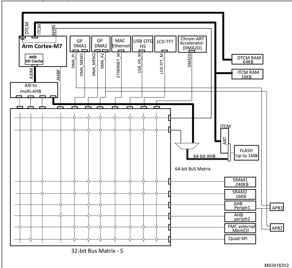
The diagram illustrates the system architecture for STM32F75xxx and STM32F74xxx devices. At the top left is the Arm Cortex-M7 core, which includes a 4KB I/D Cache . It is connected to an AXI to multi-AHB bridge via an AXIM interface. The bridge has three output paths: AHBP leading to a 32-bit Bus Matrix - S , AHBS leading to a 64-bit Bus Matrix , and ITCM leading to ITCM RAM 16KB . The 32-bit Bus Matrix - S is connected to several peripherals: GP DMA1 (DMA_PI, DMA_MEM1), GP DMA2 (DMA_P2, DMA_MEM2), MAC Ethernet (ETHERNET_M), USB OTG HS (USB_HS_M), LCD-TFT (LCD-TFT_M), and Chrom-ART Accelerator (DMA2D) (DMA2D). The 64-bit Bus Matrix is connected to DTCM RAM 64KB , FLASH Up to 1MB (via an ART bridge), SRAM1 240KB , SRAM2 16KB , AHB Periph1 (connected to APB1 ), AHB periph2 (connected to APB2 ), FMC external MemCtl (connected to APB2 ), and Quad-SPI . The DTCM interface also connects to DTCM RAM 64KB . The diagram is labeled with MS34163V2 in the bottom right corner.
The multi-AHB Bus-Matrix interconnects all the masters and slaves and it consists on:
- – 32-bit multi-AHB Bus-Matrix
- – 64-bit multi-AHB Bus-Matrix: It interconnects the 64-bit AHB bus from CPU through the AXI to AHB bridge and the 32-bit AHB bus from GP DMAs and peripheral DMAs up-sized to 64-bit to the internal flash.
The multi AHB bus matrix interconnects:
- • 12 bus masters:
- – 3x32-bit AHB bus Cortex ® -M7 AXI Master bus 64-bits, splitted 4 masters through the AXI to AHB bridge.
- – 1x64-bit AHB bus connected to the embedded flash
- – Cortex ® -M7 AHB Peripherals bus
- – DMA1 memory bus
- – DMA2 memory bus
- – DMA2 peripheral bus
- – Ethernet DMA bus
- – USB OTG HS DMA bus
- – LCD Controller DMA-bus
- – Chrom-Art Accelerator ™ (DMA2D) memory bus
- • Eight bus slaves:
- – the embedded Flash on AHB bus (for Flash read/write access, for code execution and data access)
- – Cortex ® -M7 AHBS slave interface for DMAs data transfer on DTCM RAM only.
- – Main internal SRAM1 (240 KB)
- – Auxiliary internal SRAM2 (16 KB)
- – AHB1peripherals including AHB to APB bridges and APB peripherals
- – AHB2 peripherals including AHB to APB bridges and APB peripherals
- – FMC
- – Quad SPI
2.1.1 Multi AHB BusMatrix
The multi AHB BusMatrix manages the access arbitration between masters. The arbitration uses a round-robin algorithm.
It provides access from a master to a slave, enabling concurrent access and efficient operation even when several high-speed peripherals work simultaneously.
The DTCM and ITCM RAMs (tightly coupled memories) are not part of the bus matrix.
The Data TCM RAM is accessible by the GP-DMAs and peripherals DMAs through specific AHB slave bus of the CPU.
The instruction TCM RAM is reserved only for CPU. it is accessed at CPU clock speed with 0 wait states. The architecture is shown in Figure 1 .
2.1.2 AHB/APB bridges (APB)
The two AHB/APB bridges, APB1 and APB2, provide full synchronous connections between the AHB and the two APB buses, allowing flexible selection of the peripheral frequency.
Refer to the device datasheets for more details on APB1 and APB2 maximum frequencies, and to Table 1 for the address mapping of AHB and APB peripherals.
After each device reset, all peripheral clocks are disabled (except for the SRAM, DTCM, ITCM RAM and Flash memory interface). Before using a peripheral its clock has to be enabled in the RCC_AHBxENR or RCC_APBxENR register.
Note: When a 16- or an 8-bit access is performed on an APB register, the access is transformed into a 32-bit access: the bridge duplicates the 16- or 8-bit data to feed the 32-bit vector.
2.1.3 CPU AXIM bus
This bus connects the Instruction and data bus of the Cortex ® -M7 with FPU core to the multi-AHB Bus-Matrix through AXI to AHB bridge. There are 4 AXI bus accesses:
- – CPU AXI bus access 1: The target of this AXI bus is the external memory FMC containing code or data. For the NAND Bank mapped at address 0x8000 0000 to 0x8FFF FFFF, the MPU memory attribute for this space must be reconfigured by software to Device.
- – CPU AXI bus access 2: The target of this AXI bus is the external memory Quad SPI containing code or data.
- – CPU AXI bus access 3: The target of this AXI bus is the internal SRAMs (SRAM1 and SRAM2) containing code or data.
- – CPU AXI bus access 4: The target of this AXI bus is the embedded Flash mapped on AXI interface containing code or data.
2.1.4 ITCM bus
This bus is used by the Cortex ® -M7 for instruction fetches and data access on the embedded flash mapped on ITCM interface and instruction fetches only on ITCM RAM.
2.1.5 DTCM bus
This bus is used by the Cortex ® -M7 for data access on the DTCM RAM. It can be also used for instruction fetches.
2.1.6 CPU AHBS bus
This bus connects the AHB Slave bus of the Cortex ® -M7 to the BusMatrix. This bus is used by DMAs and Peripherals DMAs for Data transfer on DTCM RAM only.
The ITCM bus is not accessible on AHBS. So the DMA data transfer to/from ITCM RAM is not supported. For DMA transfer to/from Flash on ITCM interface, all the transfers are forced through AHB bus
2.1.7 AHB peripheral bus
This bus connects the AHB Peripheral bus of the Cortex ® -M7 to the BusMatrix. This bus is used by the core to perform all data accesses to peripherals.
The target of this bus is the AHB1 peripherals including the APB peripherals and the AHB2 peripherals.
2.1.8 DMA memory bus
This bus connects the DMA memory bus master interface to the BusMatrix. It is used by the DMA to perform transfer to/from memories. The targets of this bus are data memories: internal SRAM1, SRAM2 and DTCM (through the AHBS bus of Cortex ® -M7) internal Flash memory and external memories through the FMC or Quad SPI.
2.1.9 DMA peripheral bus
This bus connects the DMA peripheral master bus interface to the BusMatrix. This bus is used by the DMA to access AHB peripherals or to perform memory-to-memory transfers. The targets of this bus are the AHB and APB peripherals plus data memories: internal SRAM1, SRAM2 and DTCM (through the AHBS bus of Cortex ® -M7) internal Flash memory and external memories through the FMC or Quad SPI.
2.1.10 Ethernet DMA bus
This bus connects the Ethernet DMA master interface to the BusMatrix. This bus is used by the Ethernet DMA to load/store data to a memory. The targets of this bus are data memories: internal SRAM1, SRAM2 and DTCM (through the AHBS bus of Cortex ® -M7) internal Flash memory, and external memories through the FMC or Quad SPI.
2.1.11 USB OTG HS DMA bus
This bus connects the USB OTG HS DMA master interface to the BusMatrix. This bus is used by the USB OTG DMA to load/store data to a memory. The targets of this bus are data memories: internal SRAM1, SRAM2 and DTCM (through the AHBS bus of Cortex ® -M7), internal Flash memory, and external memories through the FMC or Quad SPI.
2.1.12 LCD-TFT controller DMA bus
This bus connects the LCD controller DMA master interface to the BusMatrix. It is used by the LCD-TFT DMA to load data from a memory. The targets of this bus are data memories: internal SRAM1, SRAM2 and DTCM (through the AHBS bus of Cortex ® -M7), external memories through FMC or Quad SPI, and internal Flash memory.
2.1.13 DMA2D bus
This bus connects the DMA2D master interface to the BusMatrix. This bus is used by the DMA2D graphic Accelerator to load/store data to a memory. The targets of this bus are data memories: internal SRAM1, SRAM2 and DTCM (through the AHBS bus of Cortex ® -M7), external memories through FMC or Quad SPI, and internal Flash memory.
2.2 Memory organization
2.2.1 Introduction
Program memory, data memory, registers and I/O ports are organized within the same linear 4-Gbyte address space.
The bytes are coded in memory in Little Endian format. The lowest numbered byte in a word is considered the word's least significant byte and the highest numbered byte the most significant.
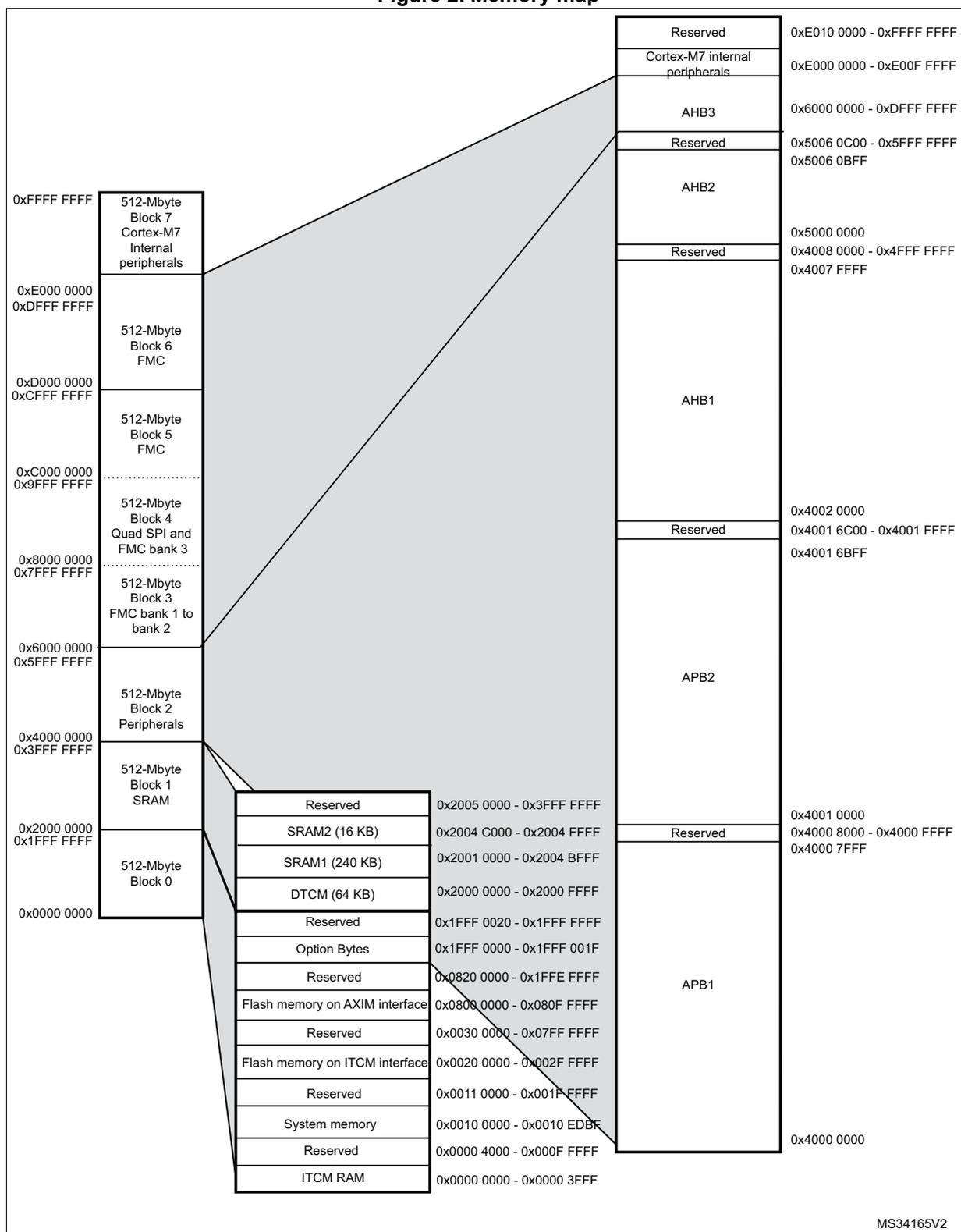
The addressable memory space is divided into eight main blocks, of 512 Mbytes each.
2.2.2 Memory map and register boundary addresses
Figure 2. Memory map
| Address Range | Memory Block / Component | Bus Interface | Address Range (Right Column) |
|---|---|---|---|
| 0x0000 0000 - 0x0000 3FFF | ITCM RAM | APB1 | 0x0000 0000 - 0x0000 3FFF |
| 0x0000 4000 - 0x0000 FFFF | Reserved | 0x0000 4000 - 0x0000 FFFF | |
| 0x0010 0000 - 0x0010 EDBF | System memory | 0x0010 0000 - 0x0010 EDBF | |
| 0x0011 0000 - 0x0011 FFFF | Reserved | 0x0011 0000 - 0x0011 FFFF | |
| 0x0020 0000 - 0x002F FFFF | Flash memory on ITCM interface | 0x0020 0000 - 0x002F FFFF | |
| 0x0030 0000 - 0x007F FFFF | Reserved | 0x0030 0000 - 0x007F FFFF | |
| 0x0800 0000 - 0x080F FFFF | Flash memory on AXIM interface | 0x0800 0000 - 0x080F FFFF | |
| 0x0820 0000 - 0x1FFE FFFF | Reserved | 0x0820 0000 - 0x1FFE FFFF | |
| 0x1FFF 0000 - 0x1FFF 001F | Option Bytes | 0x1FFF 0000 - 0x1FFF 001F | |
| 0x1FFF 0020 - 0x1FFF FFFF | Reserved | 0x1FFF 0020 - 0x1FFF FFFF | |
| 0x2000 0000 - 0x2000 FFFF | DTCM (64 KB) | 0x2000 0000 - 0x2000 FFFF | |
| 0x2001 0000 - 0x2004 BFFF | SRAM1 (240 KB) | 0x2001 0000 - 0x2004 BFFF | |
| 0x2005 0000 - 0x3FFF FFFF | Reserved | 0x2005 0000 - 0x3FFF FFFF | |
| 0x2004 C000 - 0x2004 FFFF | SRAM2 (16 KB) | Reserved | 0x2004 C000 - 0x2004 FFFF |
| 0x4000 0000 - 0x4000 7FFF | 512-Mbyte Block 0 | 0x4000 0000 - 0x4000 7FFF | |
| 0x4000 8000 - 0x4000 FFFF | Reserved | APB2 | 0x4000 8000 - 0x4000 FFFF |
| 0x4001 0000 - 0x4001 6BFF | 512-Mbyte Block 1 SRAM | 0x4001 0000 - 0x4001 6BFF | |
| 0x4001 6C00 - 0x4001 FFFF | Reserved | Reserved | 0x4001 6C00 - 0x4001 FFFF |
| 0x4002 0000 - 0x4007 FFFF | 512-Mbyte Block 2 Peripherals | 0x4002 0000 - 0x4007 FFFF | |
| 0x5000 0000 - 0x5006 0C00 | 512-Mbyte Block 3 FMC bank 1 to bank 2 | AHB1 | 0x5000 0000 - 0x5006 0C00 |
| 0x5006 0C00 - 0x5006 0BFF | Reserved | 0x5006 0C00 - 0x5006 0BFF | |
| 0x6000 0000 - 0xDFFF FFFF | 512-Mbyte Block 4 Quad SPI and FMC bank 3 | AHB2 | 0x6000 0000 - 0xDFFF FFFF |
| 0xE000 0000 - 0xE00F FFFF | Cortex-M7 internal peripherals | 0xE000 0000 - 0xE00F FFFF | |
| 0xE010 0000 - 0xFFFF FFFF | Reserved | Reserved | 0xE010 0000 - 0xFFFF FFFF |
MS34165V2
All the memory map areas that are not allocated to on-chip memories and peripherals are considered “Reserved”. For the detailed mapping of available memory and register areas, refer to the following table.
The following table gives the boundary addresses of the peripherals available in the devices.
Table 1. STM32F75xxx and STM32F74xxx register boundary addresses
| Boundary address | Peripheral | Bus | Register map |
|---|---|---|---|
| 0xA000 1000 - 0xA000 1FFF | QuadSPI Control Register | AHB3 | Section 14.5.14: QUADSPI register map on page 411 |
| 0xA000 0000 - 0xA000 0FFF | FMC control register | Section 13.8.6: FMC register map on page 382 | |
| 0x5006 0800 - 0x5006 0BFF | RNG | AHB2 | Section 19.7.4: RNG register map on page 547 |
| 0x5006 0400 - 0x5006 07FF | HASH | Section 21.6.8: HASH register map on page 633 | |
| 0x5006 0000 - 0x5006 03FF | CRYP | Section 20.7.21: CRYP register map on page 611 | |
| 0x5005 0000 - 0x5005 03FF | DCMI | Section 17.5.12: DCMI register map on page 503 | |
| 0x5000 0000 - 0x5003 FFFF | USB OTG FS | Section 37.15.64: OTG_FS/OTG_HS register map on page 1438 | |
| 0x4004 0000 - 0x4007 FFFF | USB OTG HS | AHB1 | Section 37.15.64: OTG_FS/OTG_HS register map on page 1438 |
| 0x4002 B000 - 0x4002 BBFF | Chrom-ART (DMA2D) | Section 9.5.26: DMA2D register map on page 288 | |
| 0x4002 8000 - 0x4002 93FF | ETHERNET MAC | Section 38.8.5: Ethernet register maps on page 1634 | |
| 0x4002 6400 - 0x4002 67FF | DMA2 | Section 8.5.11: DMA register map on page 257 | |
| 0x4002 6000 - 0x4002 63FF | DMA1 | ||
| 0x4002 4000 - 0x4002 4FFF | BKPSRAM | Section 5.3.27: RCC register map on page 198 | |
| 0x4002 3C00 - 0x4002 3FFF | Flash interface register | Section 3.7.8: Flash interface register map | |
| 0x4002 3800 - 0x4002 3BFF | RCC | Section 5.3.27: RCC register map on page 198 | |
| 0x4002 3000 - 0x4002 33FF | CRC | Section 12.4.6: CRC register map on page 308 | |
| 0x4002 2800 - 0x4002 2BFF | GPIOK | Section 6.4.11: GPIO register map on page 218 | |
| 0x4002 2400 - 0x4002 27FF | GPIOJ | ||
| 0x4002 2000 - 0x4002 23FF | GPIOI | ||
| 0x4002 1C00 - 0x4002 1FFF | GPIOH | ||
| 0x4002 1800 - 0x4002 1BFF | GPIOG | ||
| 0x4002 1400 - 0x4002 17FF | GPIOF | ||
| 0x4002 1000 - 0x4002 13FF | GPIOE | ||
| 0x4002 0C00 - 0x4002 0FFF | GPIO_D | ||
| 0x4002 0800 - 0x4002 0BFF | GPIOC | ||
| 0x4002 0400 - 0x4002 07FF | GPIOB | ||
| 0x4002 0000 - 0x4002 03FF | GPIOA | ||
Table 1. STM32F75xxx and STM32F74xxx register boundary addresses (continued)
| Boundary address | Peripheral | Bus | Register map |
|---|---|---|---|
| 0x4000 7C00 - 0x4000 7FFF | UART8 | Section 31.8.12: USART register map on page 1072 | |
| 0x4000 7800 - 0x4000 7BFF | UART7 | ||
| 0x4000 7400 - 0x4000 77FF | DAC | Section 16.5.15: DAC register map on page 481 | |
| 0x4000 7000 - 0x4000 73FF | PWR | Section 4.4.4: PWR power control register 2 (PWR_CSR2) on page 130 | |
| 0x4000 6C00 - 0x4000 6FFF | HDMI-CEC | Section 39.7.7: HDMI-CEC register map on page 1655 | |
| 0x4000 6800 - 0x4000 6BFF | CAN2 | ||
| 0x4000 6400 - 0x4000 67FF | CAN1 | Section 36.9.5: bxCAN register map on page 1319 | |
| 0x4000 6000 - 0x4000 63FF | I2C4 | Section 30.9.12: I2C register map on page 1009 | |
| 0x4000 5C00 - 0x4000 5FFF | I2C3 | ||
| 0x4000 5800 - 0x4000 5BFF | I2C2 | Section 30.9.12: I2C register map on page 1009 | |
| 0x4000 5400 - 0x4000 57FF | I2C1 | ||
| 0x4000 5000 - 0x4000 53FF | UART5 | ||
| 0x4000 4C00 - 0x4000 4FFF | UART4 | Section 31.8.12: USART register map on page 1072 | |
| 0x4000 4800 - 0x4000 4BFF | USART3 | ||
| 0x4000 4400 - 0x4000 47FF | USART2 | ||
| 0x4000 4000 - 0x4000 43FF | SPDIFRX | APB1 | Section 34.5.10: SPDIFRX interface register map on page 1218 |
| 0x4000 3C00 - 0x4000 3FFF | SPI3 / I2S3 | ||
| 0x4000 3800 - 0x4000 3BFF | SPI2 / I2S2 | Section 32.9.10: SPI/I2S register map on page 1132 | |
| 0x4000 3000 - 0x4000 33FF | IWDG | Section 27.4.6: IWDG register map on page 895 | |
| 0x4000 2C00 - 0x4000 2FFF | WWDG | Section 28.5.4: WWDG register map on page 901 | |
| 0x4000 2800 - 0x4000 2BFF | RTC & BKP Registers | Section 29.6.21: RTC register map on page 945 | |
| 0x4000 2400 - 0x4000 27FF | LPTIM1 | Section 26.7.9: LPTIM register map on page 886 | |
| 0x4000 2000 - 0x4000 23FF | TIM14 | ||
| 0x4000 1C00 - 0x4000 1FFF | TIM13 | Section 24.5.13: TIM10/TIM11/TIM13/TIM14 register map on page 851 | |
| 0x4000 1800 - 0x4000 1BFF | TIM12 | Section 24.4.14: TIM9/TIM12 register map on page 840 | |
| 0x4000 1400 - 0x4000 17FF | TIM7 | ||
| 0x4000 1000 - 0x4000 13FF | TIM6 | Section 25.4.9: TIMx register map on page 865 | |
| 0x4000 0C00 - 0x4000 0FFF | TIM5 | ||
| 0x4000 0800 - 0x4000 0BFF | TIM4 | ||
| 0x4000 0400 - 0x4000 07FF | TIM3 | Section 23.4.24: TIMx register map on page 800 | |
| 0x4000 0000 - 0x4000 03FF | TIM2 |
2.3 Embedded SRAM
The STM32F75xxx and STM32F74xxx feature:
- • System SRAM up to 320 Kbytes including Data TCM RAM 64 Kbytes
- • Instruction RAM (ITCM-RAM) 16 Kbytes.
- • 4 Kbytes of backup SRAM (see section 5.1.2: Battery backup domain)
The embedded SRAM is divided into up to four blocks:
- • System SRAM:
- – SRAM1 mapped at address 0x2001 0000 and accessible by all AHB masters from AHB bus Matrix.
- – SRAM2 mapped at address 0x2004 C000 and accessible by all AHB masters from AHB bus Matrix.
- – DTCM-RAM on TCM interface (Tightly Coupled Memory interface) mapped at address 0x2000 0000 and accessible by all AHB masters from AHB bus Matrix but through a specific AHB slave bus of the CPU.
- • Instruction SRAM:
- – Instruction RAM (ITCM-RAM) mapped at address 0x0000 0000 and accessible only by CPU.
The SRAM1 and SRAM2 can be accessed as bytes, half-words (16 bits) or full words (32 bits). While DTCM and ITCM RAMs can be accessed as bytes, half-words (16 bits), full words (32 bits) or double words (64 bits). These memories can be addressed at maximum system clock frequency without wait state.
The AHB masters support concurrent SRAM accesses (from the Ethernet or the USB OTG HS): for instance, the Ethernet MAC can read/write from/to SRAM2 while the CPU is reading/writing from/to SRAM1.
2.4 Flash memory overview
The Flash memory interface manages CPU AXI and TCM accesses to the Flash memory. It implements the erase and program Flash memory operations and the read and write protection mechanisms. It accelerates code execution with ART on TCM interface or L1-Cache on AXIM interface.
The Flash memory is organized as follows:
- • A main memory block divided into sectors.
- • An information block:
- – System memory from which the device boots in System memory boot mode
- – 1024 OTP (one-time programmable) bytes for user data.
- – Option bytes to configure read and write protection, BOR level, software/hardware watchdog, boot memory base address and reset when the device is in Standby or Stop mode.
Refer to Section 3: Embedded Flash memory (FLASH) for more details.
2.5 Boot configuration
In the STM32F75xxx and STM32F74xxx, two different boot areas can be selected through the BOOT pin and the boot base address programmed in the BOOT_ADD0 and BOOT_ADD1 option bytes as shown in the Table 2 .
Table 2. Boot modes
| Boot mode selection | Boot area | |
|---|---|---|
| BOOT | Boot address option bytes | |
| 0 | BOOT_ADD0[15:0] | Boot address defined by user option byte BOOT_ADD0[15:0] ST programmed value: Flash on ITCM at 0x0020 0000 |
| 1 | BOOT_ADD1[15:0] | Boot address defined by user option byte BOOT_ADD1[15:0] ST programmed value: System bootloader at 0x0010 0000 |
The values on the BOOT pin are latched on the 4th rising edge of SYSCLK after reset release. It is up to the user to set the BOOT pin after reset.
The BOOT pin is also resampled when the device exits the Standby mode. Consequently, they must be kept in the required Boot mode configuration when the device is in the Standby mode.
After startup delay, the selection of the boot area is done before releasing the processor reset.
The BOOT_ADD0 and BOOT_ADD1 address option bytes allows to program any boot memory address from 0x0000 0000 to 0x2004 FFFF which includes:
- • All Flash address space mapped on ITCM or AXIM interface
- • All RAM address space: ITCM, DTCM RAMs and SRAMs mapped on AXIM interface
- • The System memory bootloader
The BOOT_ADD0 / BOOT_ADD1 option bytes can be modified after reset in order to boot from any other boot address after next reset.
If the programmed boot memory address is out of the memory mapped area or a reserved area, the default boot fetch address is programmed as follows:
- – Boot address 0: ITCM-FLASH at 0x0020 0000
- – Boot address 1: ITCM-RAM at 0x0000 0000
When flash level 2 protection is enabled, only boot from Flash (on ITCM or AXIM interface) or system bootloader will be available. If the already programmed boot address in the BOOT_ADD0 and/or BOOT_ADD1 option bytes is out of the memory range or RAM address (on ITCM or AXIM) the default fetch will be forced from Flash on ITCM interface at address 0x00200000.
Embedded bootloader
The embedded bootloader code is located in the system memory. It is programmed by ST during production. For full information, refer to the application note (AN2606) STM32 microcontroller system memory boot mode.
By default, when the boot from system bootloader is selected, the code is executed from TCM interface. It could be executed from AXIM interface by reprogramming the BOOT_ADDx address option bytes to 0x1FF0 0000.