19. Universal synchronous asynchronous receiver transmitter (USART)
19.1 USART introduction
The universal synchronous asynchronous receiver transmitter (USART) offers a flexible means of full-duplex data exchange with external equipment requiring an industry standard NRZ asynchronous serial data format. The USART offers a very wide range of baud rates using a fractional baud rate generator.
It supports synchronous one-way communication and half-duplex single wire communication. It also supports the LIN (local interconnection network), Smartcard Protocol and IrDA (infrared data association) SIR ENDEC specifications, and modem operations (CTS/RTS). It allows multiprocessor communication.
High speed data communication is possible by using the DMA for multibuffer configuration.
19.2 USART main features
- • Full duplex, asynchronous communications
- • NRZ standard format (Mark/Space)
- • Configurable oversampling method by 16 or by 8 to give flexibility between speed and clock tolerance
- • Fractional baud rate generator systems
- – Common programmable transmit and receive baud rate (refer to the datasheets for the value of the baud rate at the maximum APB frequency).
- • Programmable data word length (8 or 9 bits)
- • Configurable stop bits - support for 1 or 2 stop bits
- • LIN Master Synchronous Break send capability and LIN slave break detection capability
- – 13-bit break generation and 10/11 bit break detection when USART is hardware configured for LIN
- • Transmitter clock output for synchronous transmission
- • IrDA SIR encoder decoder
- – Support for 3/16 bit duration for normal mode
- • Smartcard emulation capability
- – The Smartcard interface supports the asynchronous protocol Smartcards as defined in the ISO 7816-3 standards
- – 0.5, 1.5 stop bits for Smartcard operation
- • Single-wire half-duplex communication
- • Configurable multibuffer communication using DMA (direct memory access)
- – Buffering of received/transmitted bytes in reserved SRAM using centralized DMA
- • Separate enable bits for transmitter and receiver
- • Transfer detection flags:
- – Receive buffer full
- – Transmit buffer empty
- – End of transmission flags
- • Parity control:
- – Transmits parity bit
- – Checks parity of received data byte
- • Four error detection flags:
- – Overrun error
- – Noise detection
- – Frame error
- – Parity error
- • Ten interrupt sources with flags:
- – CTS changes
- – LIN break detection
- – Transmit data register empty
- – Transmission complete
- – Receive data register full
- – Idle line received
- – Overrun error
- – Framing error
- – Noise error
- – Parity error
- • Multiprocessor communication - enter into mute mode if address match does not occur
- • Wake up from mute mode (by idle line detection or address mark detection)
- • Two receiver wake-up modes: Address bit (MSB, 9 th bit), Idle line
19.3 USART functional description
The interface is externally connected to another device by three pins (see Figure 167 ). Any USART bidirectional communication requires a minimum of two pins: Receive Data In (RX) and Transmit Data Out (TX):
RX: Receive Data Input is the serial data input. Oversampling techniques are used for data recovery by discriminating between valid incoming data and noise.
TX: Transmit Data Output. When the transmitter is disabled, the output pin returns to its I/O port configuration. When the transmitter is enabled and nothing is to be transmitted, the TX pin is at high level. In single-wire and smartcard modes, this I/O is used to transmit and receive the data (at USART level, data are then received on SW_RX).
Through these pins, serial data is transmitted and received in normal USART mode as frames comprising:
- • An Idle Line prior to transmission or reception
- • A start bit
- • A data word (8 or 9 bits) least significant bit first
- • 0.5, 1, 1.5, 2 Stop bits indicating that the frame is complete
- • This interface uses a fractional baud rate generator - with a 12-bit mantissa and 4-bit fraction
- • A status register (USART_SR)
- • Data Register (USART_DR)
- • A baud rate register (USART_BRR) - 12-bit mantissa and 4-bit fraction.
- • A Guardtime Register (USART_GTPR) in case of Smartcard mode.
Refer to Section 19.6: USART registers on page 544 for the definitions of each bit.
The following pin is required to interface in synchronous mode:
- • CK: Transmitter clock output. This pin outputs the transmitter data clock for synchronous transmission corresponding to SPI master mode (no clock pulses on start bit and stop bit, and a software option to send a clock pulse on the last data bit). In parallel data can be received synchronously on RX. This can be used to control peripherals that have shift registers (e.g. LCD drivers). The clock phase and polarity are software programmable. In smartcard mode, CK can provide the clock to the smartcard.
The following pins are required in Hardware flow control mode:
- • CTS: Clear To Send blocks the data transmission at the end of the current transfer when high
- • RTS: Request to send indicates that the USART is ready to receive a data (when low).
Figure 167. USART block diagram
The diagram illustrates the internal architecture of the USART. At the top, the Transmit data register (TDR) and Receive data register (RDR) are shown, which interface with the CPU or DMA via PWDATA (Write) and PRDATA (Read). These registers connect to Transmit and Receive Shift Registers . The IrDA SIR ENDEC block handles TX , RX , SW_RX , IrDA_OUT , and IrDA_IN signals. A Hardware flow controller manages RTS and CTS signals. Control registers CR1 , CR2 , CR3 , and GTPR configure the USART's operation. CR1 includes bits for TXEIE, TCIE, RXNEIE, IDLEIE, TE, RE, RWU, and SBK. CR2 includes USART Address, UE, M, WAKE, PCE, PS, and PEIE. CR3 includes DMAT, DMAR, SCEN, NACK, HD, IRLP, and IREN. GTPR includes GT and PSC. The SCLK control block generates the CK signal. The Transmit control , Wake-up unit , and Receiver control blocks manage the data flow. The USART interrupt control block generates interrupts based on the SR (Status Register) flags: CTS, LBD, TXE, TC, RXNE, IDLE, ORE, NF, FE, and PE. The USART_BRR block contains the Transmitter rate control and Receiver rate control , which are configured by DIV_Mantissa and DIV_Fraction registers. The baud rate is calculated using the formula:
The SAMPLING DIVIDER is calculated as \( / [8 \times (2 - \text{OVER8})] \) . The /USARTDIV register is derived from the \( f_{PCLKx}(x=1,2) \) clock frequency.
ai16099b
19.3.1 USART character description
Word length may be selected as being either 8 or 9 bits by programming the M bit in the USART_CR1 register (see Figure 168 ).
The TX pin is in low state during the start bit. It is in high state during the stop bit.
An Idle character is interpreted as an entire frame of “1”s followed by the start bit of the next frame which contains data (The number of “1”s includes the number of stop bits).
A Break character is interpreted on receiving “0”s for a frame period. At the end of the break frame the transmitter inserts either 1 or 2 stop bits (logic “1” bit) to acknowledge the start bit.
Transmission and reception are driven by a common baud rate generator, the clock for each is generated when the enable bit is set respectively for the transmitter and receiver.
The details of each block is given below.
Figure 168. Word length programming
The diagram illustrates the timing for two word lengths: 9-bit and 8-bit, both with 1 stop bit.
9-bit word length (M bit is set), 1 Stop bit
The top diagram shows the timing for a 9-bit word length. It includes a 'Data frame' consisting of a 'Start bit', 9 data bits (Bit0 through Bit8), a 'Possible Parity bit', and a 'Stop bit'. Below the data frame is an 'Idle frame' (a continuous high state) and a 'Break frame' (a continuous low state). The 'Next data frame' begins with a 'Start bit'. A 'Clock' signal is shown as a series of pulses. A note indicates that the 'LBCL bit controls last data clock pulse'.
8-bit word length (M bit is reset), 1 Stop bit
The bottom diagram shows the timing for an 8-bit word length. It includes a 'Data frame' consisting of a 'Start bit', 8 data bits (Bit0 through Bit7), a 'Possible Parity bit', and a 'Stop bit'. Below the data frame is an 'Idle frame' (a continuous high state) and a 'Break frame' (a continuous low state). The 'Next data frame' begins with a 'Start bit'. A 'Clock' signal is shown as a series of pulses. A note indicates that the 'LBCL bit controls last data clock pulse'.
MS19822V2
19.3.2 Transmitter
The transmitter can send data words of either 8 or 9 bits depending on the M bit status. When the transmit enable bit (TE) is set, the data in the transmit shift register is output on the TX pin and the corresponding clock pulses are output on the CK pin.
Character transmission
During an USART transmission, data shifts out least significant bit first on the TX pin. In this mode, the USART_DR register consists of a buffer (TDR) between the internal bus and the transmit shift register (see Figure 167 ).
Every character is preceded by a start bit which is a logic level low for one bit period. The character is terminated by a configurable number of stop bits.
The following stop bits are supported by USART: 0.5, 1, 1.5 and 2 stop bits.
Note: The TE bit should not be reset during transmission of data. Resetting the TE bit during the transmission corrupts the data on the TX pin as the baud rate counters get frozen. The current data being transmitted are lost.
An idle frame is sent after the TE bit is enabled.
Configurable stop bits
The number of stop bits to be transmitted with every character can be programmed in Control register 2, bits 13,12.
- • 1 stop bit: This is the default value of number of stop bits.
- • 2 Stop bits: This is supported by normal USART, single-wire and modem modes.
- • 0.5 stop bit: To be used when receiving data in Smartcard mode.
- • 1.5 stop bits: To be used when transmitting and receiving data in Smartcard mode.
An idle frame transmission includes the stop bits.
A break transmission is 10 low bits followed by the configured number of stop bits (when m = 0) and 11 low bits followed by the configured number of stop bits (when m = 1). It is not possible to transmit long breaks (break of length greater than 10/11 low bits).
Figure 169. Configurable stop bits
8-bit Word length (M bit is reset)
CLOCK
Data frame
Possible parity bit
Next data frame
** LBCL bit controls last data clock pulse
a) 1 Stop Bit
Data frame
Possible Parity Bit
Next data frame
1 1/2 stop bits
b) 1 1/2 stop Bits
Data frame
Possible parity bit
Next data frame
c) 2 Stop Bits
Data frame
Possible parity bit
Next data frame
d) 1/2 Stop Bit
1/2 Stop Bit
MSV42088V1
Procedure:
- 1. Enable the USART by writing the UE bit in USART_CR1 register to 1.
- 2. Program the M bit in USART_CR1 to define the word length.
- 3. Program the number of stop bits in USART_CR2.
- 4. Select DMA enable (DMAT) in USART_CR3 if Multi buffer Communication is to take place. Configure the DMA register as explained in multibuffer communication.
- 5. Select the desired baud rate using the USART_BRR register.
- 6. Set the TE bit in USART_CR1 to send an idle frame as first transmission.
- 7. Write the data to send in the USART_DR register (this clears the TXE bit). Repeat this for each data to be transmitted in case of single buffer.
- 8. After writing the last data into the USART_DR register, wait until TC=1. This indicates that the transmission of the last frame is complete. This is required for instance when the USART is disabled or enters the Halt mode to avoid corrupting the last transmission.
Single byte communication
Clearing the TXE bit is always performed by a write to the data register.
The TXE bit is set by hardware and it indicates:
- • The data has been moved from TDR to the shift register and the data transmission has started.
- • The TDR register is empty.
- • The next data can be written in the USART_DR register without overwriting the previous data.
This flag generates an interrupt if the TXEIE bit is set.
When a transmission is taking place, a write instruction to the USART_DR register stores the data in the TDR register and which is copied in the shift register at the end of the current transmission.
When no transmission is taking place, a write instruction to the USART_DR register places the data directly in the shift register, the data transmission starts, and the TXE bit is immediately set.
If a frame is transmitted (after the stop bit) and the TXE bit is set, the TC bit goes high. An interrupt is generated if the TCIE bit is set in the USART_CR1 register.
After writing the last data into the USART_DR register, it is mandatory to wait for TC=1 before disabling the USART or causing the microcontroller to enter the low-power mode (see Figure 170: TC/TXE behavior when transmitting ).
The TC bit is cleared by the following software sequence:
- 1. A read from the USART_SR register
- 2. A write to the USART_DR register
Note: The TC bit can also be cleared by writing a '0' to it. This clearing sequence is recommended only for Multibuffer communication.
Figure 170. TC/TXE behavior when transmitting
Break characters
Setting the SBK bit transmits a break character. The break frame length depends on the M bit (see Figure 168 ).
If the SBK bit is set to '1' a break character is sent on the TX line after completing the current character transmission. This bit is reset by hardware when the break character is completed (during the stop bit of the break character). The USART inserts a logic 1 bit at the end of the last break frame to guarantee the recognition of the start bit of the next frame.
Note: If the software resets the SBK bit before the commencement of break transmission, the break character is not transmitted. For two consecutive breaks, the SBK bit should be set after the stop bit of the previous break.
Idle characters
Setting the TE bit drives the USART to send an idle frame before the first data frame.
19.3.3 Receiver
The USART can receive data words of either 8 or 9 bits depending on the M bit in the USART_CR1 register.
Start bit detection
The start bit detection sequence is the same when oversampling by 16 or by 8.
In the USART, the start bit is detected when a specific sequence of samples is recognized. This sequence is: 1 1 1 0 X 0 X 0 X 0 0 0 0.
Figure 171. Start bit detection when oversampling by 16 or 8
The diagram illustrates the start bit detection process. The RX line transitions from a high idle state to a low start bit. Sampling occurs at regular intervals. The 'Ideal sample clock' has 16 samples per bit, while the 'Real sample clock' has 8 samples per bit. The 'Conditions to validate the start bit' row shows the logic levels at each sampling point. The first three samples (1, 1, 1) must be high. The fourth sample (0) must be low. The subsequent samples (X, 0, X, 0, X, 0, 0, 0, 0) are used to validate the start bit. The 'Falling edge detection' occurs at the transition from the third high sample to the first low sample. The 'At least 2 bits out of 3 at 0' condition is met for the first sampling (samples 3, 5, 7) and the second sampling (samples 8, 9, 10).
| Sample Index | 1 | 2 | 3 | 4 | 5 | 6 | 7 | 8 | 9 | 10 | 11 | 12 | 13 | 14 | 15 | 16 |
|---|---|---|---|---|---|---|---|---|---|---|---|---|---|---|---|---|
| Logic Level | 1 | 1 | 1 | 0 | X | 0 | X | 0 | 0 | 0 | X | X | X | X | X | X |
| Condition | At least 2 bits out of 3 at 0 | At least 2 bits out of 3 at 0 | At least 2 bits out of 3 at 0 |
Note: If the sequence is not complete, the start bit detection aborts and the receiver returns to the idle state (no flag is set), where it waits for a falling edge.
The start bit is confirmed (RXNE flag set, interrupt generated if RXNEIE=1) if the three sampled bits are at 0 (first sampling on the third, fifth and seventh bit finds the three bits at 0 and second sampling on the eighth, ninth and tenth bit also finds the three bits at 0).
The start bit is validated (RXNE flag set, interrupt generated if RXNEIE=1) but the NE noise flag is set if, for both samplings, at least two out of the three sampled bits are at 0 (sampling on the third, fifth and seventh bit and sampling on the eighth, ninth and tenth bit). If this
condition is not met, the start detection aborts and the receiver returns to the idle state (no flag is set).
If, for one of the samplings (on the third, fifth and seventh bit, or on the eighth, ninth and tenth bit), two out of the three bits are found at 0, the start bit is validated but the NE noise flag bit is set.
Character reception
During an USART reception, data shifts in least significant bit first through the RX pin. In this mode, the USART_DR register consists of a buffer (RDR) between the internal bus and the received shift register.
Procedure:
- 1. Enable the USART by writing the UE bit in USART_CR1 register to 1.
- 2. Program the M bit in USART_CR1 to define the word length.
- 3. Program the number of stop bits in USART_CR2.
- 4. Select DMA enable (DMAR) in USART_CR3 if multibuffer communication is to take place. Configure the DMA register as explained in multibuffer communication. STEP 3
- 5. Select the desired baud rate using the baud rate register USART_BRR
- 6. Set the RE bit USART_CR1. This enables the receiver which begins searching for a start bit.
When a character is received
- • The RXNE bit is set. It indicates that the content of the shift register is transferred to the RDR. In other words, data has been received and can be read (as well as its associated error flags).
- • An interrupt is generated if the RXNEIE bit is set.
- • The error flags can be set if a frame error, noise or an overrun error has been detected during reception.
- • In multibuffer, RXNE is set after every byte received and is cleared by the DMA read to the Data Register.
- • In single buffer mode, clearing the RXNE bit is performed by a software read to the USART_DR register. The RXNE flag can also be cleared by writing a zero to it. The RXNE bit must be cleared before the end of the reception of the next character to avoid an overrun error.
Note: The RE bit should not be reset while receiving data. If the RE bit is disabled during reception, the reception of the current byte is aborted.
Break character
When a break character is received, the USART handles it as a framing error.
Idle character
When an idle frame is detected, there is the same procedure as a data received character plus an interrupt if the IDLEIE bit is set.
Overrun error
An overrun error occurs when a character is received when RXNE has not been reset. Data can not be transferred from the shift register to the RDR register until the RXNE bit is cleared.
The RXNE flag is set after every byte received. An overrun error occurs if RXNE flag is set when the next data is received or the previous DMA request has not been serviced. When an overrun error occurs:
- • The ORE bit is set.
- • The RDR content is not lost. The previous data is available when a read to USART_DR is performed.
- • The shift register is overwritten. After that point, any data received during overrun is lost.
- • An interrupt is generated if either the RXNEIE bit is set or both the EIE and DMAR bits are set.
- • The ORE bit is reset by a read to the USART_SR register followed by a USART_DR register read operation.
Note: The ORE bit, when set, indicates that at least 1 data has been lost. There are two possibilities:
- • if RXNE=1, then the last valid data is stored in the receive register RDR and can be read,
- • if RXNE=0, then it means that the last valid data has already been read and thus there is nothing to be read in the RDR. This case can occur when the last valid data is read in the RDR at the same time as the new (and lost) data is received. It may also occur when the new data is received during the reading sequence (between the USART_SR register read access and the USART_DR read access).
Selecting the proper oversampling method
The receiver implements different user-configurable oversampling techniques (except in synchronous mode) for data recovery by discriminating between valid incoming data and noise.
The oversampling method can be selected by programming the OVER8 bit in the USART_CR1 register and can be either 16 or 8 times the baud rate clock ( Figure 172 and Figure 173 ).
Depending on the application:
- • select oversampling by 8 (OVER8=1) to achieve higher speed (up to \( f_{PCLK}/8 \) ). In this case the maximum receiver tolerance to clock deviation is reduced (refer to Section 19.3.5: USART receiver tolerance to clock deviation on page 525 )
- • select oversampling by 16 (OVER8=0) to increase the tolerance of the receiver to clock deviations. In this case, the maximum speed is limited to maximum \( f_{PCLK}/16 \)
Programming the ONEBIT bit in the USART_CR3 register selects the method used to evaluate the logic level. There are two options:
- • the majority vote of the three samples in the center of the received bit. In this case, when the 3 samples used for the majority vote are not equal, the NF bit is set
- • a single sample in the center of the received bit
Depending on the application:
- – select the three samples' majority vote method (ONEBIT=0) when operating in a noisy environment and reject the data when a noise is detected (refer to Figure 72 ) because this indicates that a glitch occurred during the sampling.
- – select the single sample method (ONEBIT=1) when the line is noise-free to increase the receiver's tolerance to clock deviations (see Section 19.3.5: USART receiver tolerance to clock deviation on page 525 ). In this case the NF bit is never set.
When noise is detected in a frame:
- • The NF bit is set at the rising edge of the RXNE bit.
- • The invalid data is transferred from the Shift register to the USART_DR register.
- • No interrupt is generated in case of single byte communication. However this bit rises at the same time as the RXNE bit which itself generates an interrupt. In case of multibuffer communication an interrupt is issued if the EIE bit is set in the USART_CR3 register.
The NF bit is reset by a USART_SR register read operation followed by a USART_DR register read operation.
Note: Oversampling by 8 is not available in the Smartcard, IrDA and LIN modes. In those modes, the OVER8 bit is forced to '0' by hardware.
Figure 172. Data sampling when oversampling by 16
The diagram illustrates the timing for data sampling when oversampling by 16. The RX line is shown at the top, and the Sample clock is shown below it. The Sample clock has 16 rising edges per bit time, labeled 1 through 16. The RX line is sampled at each rising edge. The first 7 samples (1-7) are used to determine the start of the bit. The next 3 samples (8-10) are the 'sampled values' used for the majority vote. The remaining 6 samples (11-16) are used to determine the end of the bit. The bit time is divided into 16 equal parts. The first 7/16 of the bit time corresponds to the first 7 samples. The next 6/16 of the bit time corresponds to the 6 samples used for the majority vote (samples 8 through 13). The final 7/16 of the bit time corresponds to the last 7 samples (samples 14 through 16 and the start of the next bit). The diagram also shows the start and end of the bit time, and the MSv31152V1 identifier.
Figure 173. Data sampling when oversampling by 8
The diagram shows the RX line and Sample clock (x8) over one bit time. The RX line has a pulse. The Sample clock (x8) has 8 rising edges labeled 1 through 8. Samples are taken at edges 4, 5, and 6, labeled 'sampled values'. The time from the start of the bit to the start of the sampled values is 3/8 of a bit time. The duration of the sampled values is 2/8 of a bit time. The time from the end of the sampled values to the end of the bit time is 3/8 of a bit time. The total bit time is labeled 'One bit time'. The diagram is labeled MSv31153V1.
Table 72. Noise detection from sampled data
| Sampled value | NE status | Received bit value |
|---|---|---|
| 000 | 0 | 0 |
| 001 | 1 | 0 |
| 010 | 1 | 0 |
| 011 | 1 | 1 |
| 100 | 1 | 0 |
| 101 | 1 | 1 |
| 110 | 1 | 1 |
| 111 | 0 | 1 |
Framing error
A framing error is detected when:
The stop bit is not recognized on reception at the expected time, following either a de-synchronization or excessive noise.
When the framing error is detected:
- • The FE bit is set by hardware
- • The invalid data is transferred from the Shift register to the USART_DR register.
- • No interrupt is generated in case of single byte communication. However this bit rises at the same time as the RXNE bit which itself generates an interrupt. In case of multibuffer communication an interrupt is issued if the EIE bit is set in the USART_CR3 register.
The FE bit is reset by a USART_SR register read operation followed by a USART_DR register read operation.
Configurable stop bits during reception
The number of stop bits to be received can be configured through the control bits of Control Register 2 - it can be either 1 or 2 in normal mode and 0.5 or 1.5 in Smartcard mode.
- 1. 0.5 stop bit (reception in Smartcard mode) : No sampling is done for 0.5 stop bit. As a consequence, no framing error and no break frame can be detected when 0.5 stop bit is selected.
- 2. 1 stop bit : Sampling for 1 stop Bit is done on the 8th, 9th and 10th samples.
- 3. 1.5 stop bits (Smartcard mode) : When transmitting in smartcard mode, the device must check that the data is correctly sent. Thus the receiver block must be enabled (RE =1 in the USART_CR1 register) and the stop bit is checked to test if the smartcard has detected a parity error. In the event of a parity error, the smartcard forces the data signal low during the sampling - NACK signal-, which is flagged as a framing error. Then, the FE flag is set with the RXNE at the end of the 1.5 stop bit. Sampling for 1.5 stop bits is done on the 16th, 17th and 18th samples (1 baud clock period after the beginning of the stop bit). The 1.5 stop bit can be decomposed into 2 parts: one 0.5 baud clock period during which nothing happens, followed by 1 normal stop bit period during which sampling occurs halfway through. Refer to Section 19.3.11: Smartcard on page 534 for more details.
- 4. 2 stop bits : Sampling for 2 stop bits is done on the 8th, 9th and 10th samples of the first stop bit. If a framing error is detected during the first stop bit the framing error flag is set. The second stop bit is not checked for framing error. The RXNE flag is set at the end of the first stop bit.
19.3.4 Fractional baud rate generation
The baud rate for the receiver and transmitter (Rx and Tx) are both set to the same value as programmed in the Mantissa and Fraction values of USARTDIV.
Equation 1: Baud rate for standard USART (SPI mode included)
Equation 2: Baud rate in Smartcard, LIN and IrDA modes
USARTDIV is an unsigned fixed point number that is coded on the USART_BRR register.
- • When OVER8=0, the fractional part is coded on 4 bits and programmed by the DIV_fraction[3:0] bits in the USART_BRR register
- • When OVER8=1, the fractional part is coded on 3 bits and programmed by the DIV_fraction[2:0] bits in the USART_BRR register, and bit DIV_fraction[3] must be kept cleared.
Note: The baud counters are updated to the new value in the baud registers after a write operation to USART_BRR. Hence the baud rate register value should not be changed during communication.
How to derive USARTDIV from USART_BRR register values when OVER8=0 Example 1:If DIV_Mantissa = 0d27 and DIV_Fraction = 0d12 (USART_BRR = 0x1BC), then
Mantissa (USARTDIV) = 0d27
Fraction (USARTDIV) = 12/16 = 0d0.75
Therefore USARTDIV = 0d27.75
Example 2:To program USARTDIV = 0d25.62
This leads to:
DIV_Fraction = 16*0d0.62 = 0d9.92
The nearest real number is 0d10 = 0xA
DIV_Mantissa = mantissa (0d25.620) = 0d25 = 0x19
Then, USART_BRR = 0x19A hence USARTDIV = 0d25.625
Example 3:To program USARTDIV = 0d50.99
This leads to:
DIV_Fraction = 16*0d0.99 = 0d15.84
The nearest real number is 0d16 = 0x10 => overflow of DIV_frac[3:0] => carry must be added up to the mantissa
DIV_Mantissa = mantissa (0d50.990 + carry) = 0d51 = 0x33
Then, USART_BRR = 0x330 hence USARTDIV = 0d51.000
How to derive USARTDIV from USART_BRR register values when OVER8=1 Example 1:If DIV_Mantissa = 0x27 and DIV_Fraction[2:0]= 0d6 (USART_BRR = 0x1B6), then
Mantissa (USARTDIV) = 0d27
Fraction (USARTDIV) = 6/8 = 0d0.75
Therefore USARTDIV = 0d27.75
Example 2:To program USARTDIV = 0d25.62
This leads to:
DIV_Fraction = 8*0d0.62 = 0d4.96
The nearest real number is 0d5 = 0x5
DIV_Mantissa = mantissa (0d25.620) = 0d25 = 0x19
Then, \( USART\_BRR = 0x195 \Rightarrow USARTDIV = 0d25.625 \)
Example 3:
To program \( USARTDIV = 0d50.99 \)
This leads to:
\( DIV\_Fraction = 8 * 0d0.99 = 0d7.92 \)
The nearest real number is \( 0d8 = 0x8 \Rightarrow \) overflow of the \( DIV\_frac[2:0] \Rightarrow \) carry must be added up to the mantissa
\( DIV\_Mantissa = \text{mantissa } (0d50.990 + \text{carry}) = 0d51 = 0x33 \)
Then, \( USART\_BRR = 0x0330 \Rightarrow USARTDIV = 0d51.000 \)
Table 73. Error calculation for programmed baud rates at \( f_{PCLK} = 8 \) MHz or \( f_{PCLK} = 12 \) MHz, oversampling by 16 (1)
| Oversampling by 16 (OVER8=0) | |||||||
|---|---|---|---|---|---|---|---|
| Baud rate 7 | \( f_{PCLK} = 8 \) MHz | \( f_{PCLK} = 12 \) MHz | |||||
| S.No | Desired | Actual | Value programmed in the baud rate register | % Error = (Calculated - Desired) B.rate / Desired B.rate | Actual | Value programmed in the baud rate register | % Error |
| 1 | 1.2 KBps | 1.2 KBps | 416.6875 | 0 | 1.2 KBps | 625 | 0 |
| 2 | 2.4 KBps | 2.4 KBps | 208.3125 | 0.01 | 2.4 KBps | 312.5 | 0 |
| 3 | 9.6 KBps | 9.604 KBps | 52.0625 | 0.04 | 9.6 KBps | 78.125 | 0 |
| 4 | 19.2 KBps | 19.185 KBps | 26.0625 | 0.08 | 19.2 KBps | 39.0625 | 0 |
| 5 | 38.4 KBps | 38.462 KBps | 13 | 0.16 | 38.339 KBps | 19.5625 | 0.16 |
| 6 | 57.6 KBps | 57.554 KBps | 8.6875 | 0.08 | 57.692 KBps | 13 | 0.16 |
| 7 | 115.2 KBps | 115.942 KBps | 4.3125 | 0.64 | 115.385 KBps | 6.5 | 0.16 |
| 8 | 230.4 KBps | 228.571 KBps | 2.1875 | 0.79 | 230.769 KBps | 3.25 | 0.16 |
| 9 | 460.8 KBps | 470.588 KBps | 1.0625 | 2.12 | 461.538 KBps | 1.625 | 0.16 |
| 10 | 921.6 KBps | NA | NA | NA | NA | NA | NA |
| 11 | 2 MBps | NA | NA | NA | NA | NA | NA |
| 12 | 3 MBps | NA | NA | NA | NA | NA | NA |
- 1. The lower the CPU clock the lower the accuracy for a particular baud rate. The upper limit of the achievable baud rate can be fixed with these data.
| Oversampling by 8 (OVER8 = 1) | |||||||
|---|---|---|---|---|---|---|---|
| Baud rate | \( f_{PCLK} = 8 \) MHz | \( f_{PCLK} = 12 \) MHz | |||||
| S.No | Desired | Actual | Value programmed in the baud rate register | % Error = (Calculated - Desired) B.rate / Desired B.rate | Actual | Value programmed in the baud rate register | % Error |
| 1 | 1.2 KBps | 1.2 KBps | 833.375 | 0 | 1.2 KBps | 1250 | 0 |
| 2 | 2.4 KBps | 2.4 KBps | 416.625 | 0.01 | 2.4 KBps | 625 | 0 |
| 3 | 9.6 KBps | 9.604 KBps | 104.125 | 0.04 | 9.6 KBps | 156.25 | 0 |
| 4 | 19.2 KBps | 19.185 KBps | 52.125 | 0.08 | 19.2 KBps | 78.125 | 0 |
| 5 | 38.4 KBps | 38.462 KBps | 26 | 0.16 | 38.339 KBps | 39.125 | 0.16 |
| 6 | 57.6 KBps | 57.554 KBps | 17.375 | 0.08 | 57.692 KBps | 26 | 0.16 |
| 7 | 115.2 KBps | 115.942 KBps | 8.625 | 0.64 | 115.385 KBps | 13 | 0.16 |
| 8 | 230.4 KBps | 228.571 KBps | 4.375 | 0.79 | 230.769 KBps | 6.5 | 0.16 |
| 9 | 460.8 KBps | 470.588 KBps | 2.125 | 2.12 | 461.538 KBps | 3.25 | 0.16 |
| 10 | 921.6 KBps | 888.889 KBps | 1.125 | 3.55 | 923.077 KBps | 1.625 | 0.16 |
| 11 | 2 MBps | NA | NA | NA | NA | NA | NA |
| 12 | 3 MBps | NA | NA | NA | NA | NA | NA |
1. The lower the CPU clock the lower the accuracy for a particular baud rate. The upper limit of the achievable baud rate can be fixed with these data.
Table 75. Error calculation for programmed baud rates at \( f_{PCLK} = 16 \) MHz or \( f_{PCLK} = 24 \) MHz, oversampling by 16 (1)| Oversampling by 16 (OVER8 = 0) | |||||||
|---|---|---|---|---|---|---|---|
| Baud rate | \( f_{PCLK} = 16 \) MHz | \( f_{PCLK} = 24 \) MHz | |||||
| S.No | Desired | Actual | Value programmed in the baud rate register | % Error = (Calculated - Desired) B.rate / Desired B.rate | Actual | Value programmed in the baud rate register | % Error |
| 1 | 1.2 KBps | 1.2 KBps | 833.3125 | 0 | 1.2 | 1250 | 0 |
| 2 | 2.4 KBps | 2.4 KBps | 416.6875 | 0 | 2.4 | 625 | 0 |
| 3 | 9.6 KBps | 9.598 KBps | 104.1875 | 0.02 | 9.6 | 156.25 | 0 |
| 4 | 19.2 KBps | 19.208 KBps | 52.0625 | 0.04 | 19.2 | 78.125 | 0 |
| 5 | 38.4 KBps | 38.369 KBps | 26.0625 | 0.08 | 38.4 | 39.0625 | 0 |
| 6 | 57.6 KBps | 57.554 KBps | 17.375 | 0.08 | 57.554 | 26.0625 | 0.08 |
Table 75. Error calculation for programmed baud rates at \( f_{PCLK} = 16 \) MHz or \( f_{PCLK} = 24 \) MHz, oversampling by 16 (1) (continued)
| Oversampling by 16 (OVER8 = 0) | |||||||
|---|---|---|---|---|---|---|---|
| Baud rate | \( f_{PCLK} = 16 \) MHz | \( f_{PCLK} = 24 \) MHz | |||||
| S.No | Desired | Actual | Value programmed in the baud rate register | % Error = (Calculated - Desired) B.rate / Desired B.rate | Actual | Value programmed in the baud rate register | % Error |
| 7 | 115.2 KBps | 115.108 KBps | 8.6875 | 0.08 | 115.385 | 13 | 0.16 |
| 8 | 230.4 KBps | 231.884 KBps | 4.3125 | 0.64 | 230.769 | 6.5 | 0.16 |
| 9 | 460.8 KBps | 457.143 KBps | 2.1875 | 0.79 | 461.538 | 3.25 | 0.16 |
| 10 | 921.6 KBps | 941.176 KBps | 1.0625 | 2.12 | 923.077 | 1.625 | 0.16 |
| 11 | 2 MBps | NA | NA | NA | NA | NA | NA |
| 12 | 3 MBps | NA | NA | NA | NA | NA | NA |
1. The lower the CPU clock the lower the accuracy for a particular baud rate. The upper limit of the achievable baud rate can be fixed with these data.
Table 76. Error calculation for programmed baud rates at \( f_{PCLK} = 16 \) MHz or \( f_{PCLK} = 24 \) MHz, oversampling by 8 (1)
| Oversampling by 8 (OVER8=1) | |||||||
|---|---|---|---|---|---|---|---|
| Baud rate | \( f_{PCLK} = 16 \) MHz | \( f_{PCLK} = 24 \) MHz | |||||
| S.No | Desired | Actual | Value programmed in the baud rate register | % Error = (Calculated - Desired) B.rate / Desired B.rate | Actual | Value programmed in the baud rate register | % Error |
| 1 | 1.2 KBps | 1.2 KBps | 1666.625 | 0 | 1.2 KBps | 2500 | 0 |
| 2 | 2.4 KBps | 2.4 KBps | 833.375 | 0 | 2.4 KBps | 1250 | 0 |
| 3 | 9.6 KBps | 9.598 KBps | 208.375 | 0.02 | 9.6 KBps | 312.5 | 0 |
| 4 | 19.2 KBps | 19.208 KBps | 104.125 | 0.04 | 19.2 KBps | 156.25 | 0 |
| 5 | 38.4 KBps | 38.369 KBps | 52.125 | 0.08 | 38.4 KBps | 78.125 | 0 |
| 6 | 57.6 KBps | 57.554 KBps | 34.75 | 0.08 | 57.554 KBps | 52.125 | 0.08 |
| 7 | 115.2 KBps | 115.108 KBps | 17.375 | 0.08 | 115.385 KBps | 26 | 0.16 |
| 8 | 230.4 KBps | 231.884 KBps | 8.625 | 0.64 | 230.769 KBps | 13 | 0.16 |
| 9 | 460.8 KBps | 457.143 KBps | 4.375 | 0.79 | 461.538 KBps | 6.5 | 0.16 |
| 10 | 921.6 KBps | 941.176 KBps | 2.125 | 2.12 | 923.077 KBps | 3.25 | 0.16 |
| 11 | 2 MBps | 2000 KBps | 1 | 0 | 2000 KBps | 1.5 | 0 |
| 12 | 3 MBps | NA | NA | NA | 3000 KBps | 1 | 0 |
1. The lower the CPU clock the lower the accuracy for a particular baud rate. The upper limit of the achievable baud rate can be fixed with these data.
Table 77. Error calculation for programmed baud rates at \( f_{PCLK} = 8 \) MHz or \( f_{PCLK} = 16 \) MHz, oversampling by 16 (1)| Oversampling by 16 (OVER8=0) | |||||||
|---|---|---|---|---|---|---|---|
| Baud rate | \( f_{PCLK} = 8 \) MHz | \( f_{PCLK} = 16 \) MHz | |||||
| S.No | Desired | Actual | Value programmed in the baud rate register | % Error = (Calculated - Desired)B.Rate /Desired B.Rate | Actual | Value programmed in the baud rate register | % Error |
| 1. | 2.4 KBps | 2.400 KBps | 208.3125 | 0.00% | 2.400 KBps | 416.6875 | 0.00% |
| 2. | 9.6 KBps | 9.604 KBps | 52.0625 | 0.04% | 9.598 KBps | 104.1875 | 0.02% |
| 3. | 19.2 KBps | 19.185 KBps | 26.0625 | 0.08% | 19.208 KBps | 52.0625 | 0.04% |
| 4. | 57.6 KBps | 57.554 KBps | 8.6875 | 0.08% | 57.554 KBps | 17.3750 | 0.08% |
| 5. | 115.2 KBps | 115.942 KBps | 4.3125 | 0.64% | 115.108 KBps | 8.6875 | 0.08% |
| 6. | 230.4 KBps | 228.571 KBps | 2.1875 | 0.79% | 231.884 KBps | 4.3125 | 0.64% |
| 7. | 460.8 KBps | 470.588 KBps | 1.0625 | 2.12% | 457.143 KBps | 2.1875 | 0.79% |
| 8. | 896 KBps | NA | NA | NA | 888.889 KBps | 1.1250 | 0.79% |
| 9. | 921.6 KBps | NA | NA | NA | 941.176 KBps | 1.0625 | 2.12% |
| 10. | 1.792 MBps | NA | NA | NA | NA | NA | NA |
| 11. | 1.8432 MBps | NA | NA | NA | NA | NA | NA |
| 12. | 3.584 MBps | NA | NA | NA | NA | NA | NA |
| 13. | 3.6864 MBps | NA | NA | NA | NA | NA | NA |
| 14. | 7.168 MBps | NA | NA | NA | NA | NA | NA |
| 15. | 7.3728 MBps | NA | NA | NA | NA | NA | NA |
1. The lower the CPU clock the lower the accuracy for a particular baud rate. The upper limit of the achievable baud rate can be fixed with these data.
Table 78. Error calculation for programmed baud rates at \( f_{PCLK} = 8 \) MHz or \( f_{PCLK} = 16 \) MHz, oversampling by 8 (1)| Oversampling by 8 (OVER8=1) | |||||||
|---|---|---|---|---|---|---|---|
| Baud rate | \( f_{PCLK} = 8 \) MHz | \( f_{PCLK} = 16 \) MHz | |||||
| S.No | Desired | Actual | Value programmed in the baud rate register | % Error = (Calculated - Desired)B.Rate /Desired B.Rate | Actual | Value programmed in the baud rate register | % Error |
| 1. | 2.4 KBps | 2.400 KBps | 416.625 | 0.01% | 2.400 KBps | 833.375 | 0.00% |
| 2. | 9.6 KBps | 9.604 KBps | 104.125 | 0.04% | 9.598 KBps | 208.375 | 0.02% |
| 3. | 19.2 KBps | 19.185 KBps | 52.125 | 0.08% | 19.208 KBps | 104.125 | 0.04% |
Table 78. Error calculation for programmed baud rates at \( f_{PCLK} = 8 \) MHz or \( f_{PCLK} = 16 \) MHz, oversampling by 8 (1) (continued)
| Oversampling by 8 (OVER8=1) | |||||||
|---|---|---|---|---|---|---|---|
| Baud rate | \( f_{PCLK} = 8 \) MHz | \( f_{PCLK} = 16 \) MHz | |||||
| S.No | Desired | Actual | Value programmed in the baud rate register | % Error = (Calculated - Desired)B.Rate /Desired B.Rate | Actual | Value programmed in the baud rate register | % Error |
| 4. | 57.6 KBps | 57.557 KBps | 17.375 | 0.08% | 57.554 KBps | 34.750 | 0.08% |
| 5. | 115.2 KBps | 115.942 KBps | 8.625 | 0.64% | 115.108 KBps | 17.375 | 0.08% |
| 6. | 230.4 KBps | 228.571 KBps | 4.375 | 0.79% | 231.884 KBps | 8.625 | 0.64% |
| 7. | 460.8 KBps | 470.588 KBps | 2.125 | 2.12% | 457.143 KBps | 4.375 | 0.79% |
| 8. | 896 KBps | 888.889 KBps | 1.125 | 0.79% | 888.889 KBps | 2.250 | 0.79% |
| 9. | 921.6 KBps | 888.889 KBps | 1.125 | 3.55% | 941.176 KBps | 2.125 | 2.12% |
| 10. | 1.792 MBps | NA | NA | NA | 1.7777 MBps | 1.125 | 0.79% |
| 11. | 1.8432 MBps | NA | NA | NA | 1.7777 MBps | 1.125 | 3.55% |
| 12. | 3.584 MBps | NA | NA | NA | NA | NA | NA |
| 13. | 3.6864 MBps | NA | NA | NA | NA | NA | NA |
| 14. | 7.168 MBps | NA | NA | NA | NA | NA | NA |
| 15. | 7.3728 MBps | NA | NA | NA | NA | NA | NA |
1. The lower the CPU clock the lower the accuracy for a particular baud rate. The upper limit of the achievable baud rate can be fixed with these data.
Table 79. Error calculation for programmed baud rates at \( f_{PCLK} = 30 \) MHz or \( f_{PCLK} = 60 \) MHz, oversampling by 16 (1)(2)
| Oversampling by 16 (OVER8=0) | |||||||
|---|---|---|---|---|---|---|---|
| Baud rate | \( f_{PCLK} = 30 \) MHz | \( f_{PCLK} = 60 \) MHz | |||||
| S.No | Desired | Actual | Value programmed in the baud rate register | % Error = (Calculated - Desired)B.Rate /Desired B.Rate | Actual | Value programmed in the baud rate register | % Error |
| 1. | 2.4 KBps | 2.400 KBps | 781.2500 | 0.00% | 2.400 KBps | 1562.5000 | 0.00% |
| 2. | 9.6 KBps | 9.600 KBps | 195.3125 | 0.00% | 9.600 KBps | 390.6250 | 0.00% |
| 3. | 19.2 KBps | 19.194 KBps | 97.6875 | 0.03% | 19.200 KBps | 195.3125 | 0.00% |
| 4. | 57.6 KBps | 57.582 KBps | 32.5625 | 0.03% | 57.582 KBps | 65.1250 | 0.03% |
| 5. | 115.2 KBps | 115.385 KBps | 16.2500 | 0.16% | 115.163 KBps | 32.5625 | 0.03% |
| 6. | 230.4 KBps | 230.769 KBps | 8.1250 | 0.16% | 230.769 KBps | 16.2500 | 0.16% |
| 7. | 460.8 KBps | 461.538 KBps | 4.0625 | 0.16% | 461.538 KBps | 8.1250 | 0.16% |
| 8. | 896 KBps | 909.091 KBps | 2.0625 | 1.46% | 895.522 KBps | 4.1875 | 0.05% |
| Oversampling by 16 (OVER8=0) | |||||||
|---|---|---|---|---|---|---|---|
| Baud rate | \( f_{PCLK} = 30 \) MHz | \( f_{PCLK} = 60 \) MHz | |||||
| S.No | Desired | Actual | Value programmed in the baud rate register | % Error = (Calculated - Desired)B.Rate /Desired B.Rate | Actual | Value programmed in the baud rate register | % Error |
| 9. | 921.6 KBps | 909.091 KBps | 2.0625 | 1.36% | 923.077 KBps | 4.0625 | 0.16% |
| 10. | 1.792 MBps | 1.1764 MBps | 1.0625 | 1.52% | 1.8182 MBps | 2.0625 | 1.36% |
| 11. | 1.8432 MBps | 1.8750 MBps | 1.0000 | 1.73% | 1.8182 MBps | 2.0625 | 1.52% |
| 12. | 3.584 MBps | NA | NA | NA | 3.2594 MBps | 1.0625 | 1.52% |
| 13. | 3.6864 MBps | NA | NA | NA | 3.7500 MBps | 1.0000 | 1.73% |
| 14. | 7.168 MBps | NA | NA | NA | NA | NA | NA |
| 15. | 7.3728 MBps | NA | NA | NA | NA | NA | NA |
- 1. The lower the CPU clock the lower the accuracy for a particular baud rate. The upper limit of the achievable baud rate can be fixed with these data.
- 2. Only USART1 and USART6 are clocked with PCLK2. Other USARTs are clocked with PCLK1. Refer to the device datasheets for the maximum values for PCLK1 and PCLK2.
| Oversampling by 8 (OVER8=1) | |||||||
|---|---|---|---|---|---|---|---|
| Baud rate | \( f_{PCLK} = 30 \) MHz | \( f_{PCLK} = 60 \) MHz | |||||
| S.No | Desired | Actual | Value programmed in the baud rate register | % Error = (Calculated - Desired)B.Rate /Desired B.Rate | Actual | Value programmed in the baud rate register | % Error |
| 1. | 2.4 KBps | 2.400 KBps | 1562.5000 | 0.00% | 2.400 KBps | 3125.0000 | 0.00% |
| 2. | 9.6 KBps | 9.600 KBps | 390.6250 | 0.00% | 9.600 KBps | 781.2500 | 0.00% |
| 3. | 19.2 KBps | 19.194 KBps | 195.3750 | 0.03% | 19.200 KBps | 390.6250 | 0.00% |
| 4. | 57.6 KBps | 57.582 KBps | 65.1250 | 0.16% | 57.582 KBps | 130.2500 | 0.03% |
| 5. | 115.2 KBps | 115.385 KBps | 32.5000 | 0.16% | 115.163 KBps | 65.1250 | 0.03% |
| 6. | 230.4 KBps | 230.769 KBps | 16.2500 | 0.16% | 230.769 KBps | 32.5000 | 0.16% |
| 7. | 460.8 KBps | 461.538 KBps | 8.1250 | 0.16% | 461.538 KBps | 16.2500 | 0.16% |
| 8. | 896 KBps | 909.091 KBps | 4.1250 | 1.46% | 895.522 KBps | 8.3750 | 0.05% |
| 9. | 921.6 KBps | 909.091 KBps | 4.1250 | 1.36% | 923.077 KBps | 8.1250 | 0.16% |
| 10. | 1.792 MBps | 1.7647 MBps | 2.1250 | 1.52% | 1.8182 MBps | 4.1250 | 1.46% |
Table 80. Error calculation for programmed baud rates at \( f_{PCLK} = 30 \) MHz or \( f_{PCLK} = 60 \) MHz, oversampling by 8 (1) (2) (continued)
| Oversampling by 8 (OVER8=1) | |||||||
|---|---|---|---|---|---|---|---|
| Baud rate | \( f_{PCLK} = 30 \) MHz | \( f_{PCLK} = 60 \) MHz | |||||
| S.No | Desired | Actual | Value programmed in the baud rate register | % Error = (Calculated - Desired)B.Rate /Desired B.Rate | Actual | Value programmed in the baud rate register | % Error |
| 11. | 1.8432 MBps | 1.8750 MBps | 2.0000 | 1.73% | 1.8182 MBps | 4.1250 | 1.36% |
| 12. | 3.584 MBps | 3.7500 MBps | 1.0000 | 4.63% | 3.5294 MBps | 2.1250 | 1.52% |
| 13. | 3.6864 MBps | 3.7500 MBps | 1.0000 | 1.73% | 3.7500 MBps | 2.0000 | 1.73% |
| 14. | 7.168 MBps | NA | NA | NA | 7.5000 MBps | 1.0000 | 4.63% |
| 15. | 7.3728 MBps | NA | NA | NA | 7.5000 MBps | 1.0000 | 1.73% |
- 1. The lower the CPU clock the lower the accuracy for a particular baud rate. The upper limit of the achievable baud rate can be fixed with these data.
- 2. Only USART1 and USART6 are clocked with PCLK2. Other USARTs are clocked with PCLK1. Refer to the device datasheets for the maximum values for PCLK1 and PCLK2.
Table 81. Error calculation for programmed baud rates at \( f_{PCLK} = 42 \) MHz or \( f_{PCLK} = 84 \) MHz, oversampling by 16 (1)(2)
| Oversampling by 16 (OVER8=0) | |||||||
|---|---|---|---|---|---|---|---|
| Baud rate | \( f_{PCLK} = 42 \) MHz | \( f_{PCLK} = 84 \) MHz | |||||
| S.No | Desired | Actual | Value programmed in the baud rate register | % Error = (Calculated - Desired)B.Rate /Desired B.Rate | Actual | Value programmed in the baud rate register | % Error |
| 1. | 1.2 KBps | 1.2 KBps | 2187.5 | 0 | 1.2 KBps | NA | 0 |
| 2. | 2.4 KBps | 2.4 KBps | 1093.75 | 0 | 2.4 KBps | 2187.5 | 0 |
| 3. | 9.6 KBps | 9.6 KBps | 273.4375 | 0 | 9.6 KBps | 546.875 | 0 |
| 4. | 19.2 KBps | 19.195 KBps | 136.75 | 0.02 | 19.2 KBps | 273.4375 | 0 |
| 5. | 38.4 KBps | 38.391 KBps | 68.375 | 0.02 | 38.391 KBps | 136.75 | 0.02 |
| 6. | 57.6 KBps | 57.613 KBps | 45.5625 | 0.02 | 57.613 KBps | 91.125 | 0.02 |
| 7. | 115.2 KBps | 115.068 KBps | 22.8125 | 0.11 | 115.226 KBps | 45.5625 | 0.02 |
| 8. | 230.4 KBps | 230.769 KBps | 11.375 | 0.16 | 230.137 KBps | 22.8125 | 0.11 |
| 9. | 460.8 KBps | 461.538 KBps | 5.6875 | 0.16 | 461.538 KBps | 11.375 | 0.16 |
| 10. | 921.6 KBps | 913.043 KBps | 2.875 | 0.93 | 923.076 KBps | 5.6875 | 0.93 |
| 11. | 1.792 MBps | 1.826 MBps | 1.4375 | 1.9 | 1.787 MBps | 2.9375 | 0.27 |
| 12. | 1.8432 MBps | 1.826 MBps | 1.4375 | 0.93 | 1.826 MBps | 2.875 | 0.93 |
| 13. | 3.584 MBps | N.A | N.A | N.A | 3.652 MBps | 1.4375 | 1.9 |
| 14. | 3.6864 MBps | N.A | N.A | N.A | 3.652 MBps | 1.4375 | 0.93 |
| Oversampling by 16 (OVER8=0) | |||||||
|---|---|---|---|---|---|---|---|
| Baud rate | \( f_{PCLK} = 42 \) MHz | \( f_{PCLK} = 84 \) MHz | |||||
| S.No | Desired | Actual | Value programmed in the baud rate register | % Error = (Calculated - Desired)B.Rate /Desired B.Rate | Actual | Value programmed in the baud rate register | % Error |
| 15. | 7.168 MBps | N.A | N.A | N.A | N.A | N.A | N.A |
| 16. | 7.3728 MBps | N.A | N.A | N.A | N.A | N.A | N.A |
| 17. | 9 MBps | N.A | N.A | N.A | N.A | N.A | N.A |
| 18. | 10.5 MBps | N.A | N.A | N.A | N.A | N.A | N.A |
- 1. The lower the CPU clock the lower the accuracy for a particular baud rate. The upper limit of the achievable baud rate can be fixed with these data.
- 2. Only USART1 and USART6 are clocked with PCLK2. Other USARTs are clocked with PCLK1. Refer to the device datasheets for the maximum values for PCLK1 and PCLK2.
| Oversampling by 8 (OVER8=1) | |||||||
|---|---|---|---|---|---|---|---|
| Baud rate | \( f_{PCLK} = 42 \) MHz | \( f_{PCLK} = 84 \) MHz | |||||
| S.No | Desired | Actual | Value programmed in the baud rate register | Value programmed in the baud rate register | Actual | Value programmed in the baud rate register | % Error |
| 1. | 2.4 KBps | 2.4 KBps | 2187.5 | 0 | 2.4 KBps | NA | 0 |
| 2. | 9.6 KBps | 9.6 KBps | 546.875 | 0 | 9.6 KBps | 1093.75 | 0 |
| 3. | 19.2 KBps | 19.195 KBps | 273.5 | 0.02 | 19.2 KBps | 546.875 | 0 |
| 4. | 38.4 KBps | 38.391 KBps | 136.75 | 0.02 | 38.391 KBps | 273.5 | 0.02 |
| 5. | 57.6 KBps | 57.613 KBps | 91.125 | 0.02 | 57.613 KBps | 182.25 | 0.02 |
| 6. | 115.2 KBps | 115.068 KBps | 45.625 | 0.11 | 115.226 KBps | 91.125 | 0.02 |
| 7. | 230.4 KBps | 230.769 KBps | 22.75 | 0.11 | 230.137 KBps | 45.625 | 0.11 |
| 8. | 460.8 KBps | 461.538 KBps | 11.375 | 0.16 | 461.538 KBps | 22.75 | 0.16 |
| 9. | 921.6 KBps | 913.043 KBps | 5.75 | 0.93 | 923.076 KBps | 11.375 | 0.93 |
| 10. | 1.792 MBps | 1.826 MBps | 2.875 | 1.9 | 1.787 Mbps | 5.875 | 0.27 |
| 11. | 1.8432 MBps | 1.826 MBps | 2.875 | 0.93 | 1.826 MBps | 5.75 | 0.93 |
| 12. | 3.584 MBps | 3.5 MBps | 1.5 | 2.34 | 3.652 MBps | 2.875 | 1.9 |
| 13. | 3.6864 MBps | 3.82 MBps | 1.375 | 3.57 | 3.652 MBps | 2.875 | 0.93 |
| 14. | 7.168 MBps | N.A | N.A | N.A | 7 MBps | 1.5 | 2.34 |
| 15. | 7.3728 MBps | N.A | N.A | N.A | 7.636 MBps | 1.375 | 3.57 |
Table 82. Error calculation for programmed baud rates at \( f_{PCLK} = 42 \) MHz or \( f_{PCLK} = 84 \) MHz, oversampling by 8 (1)(2) (continued)
| Oversampling by 8 (OVER8=1) | |||||||
|---|---|---|---|---|---|---|---|
| Baud rate | \( f_{PCLK} = 42 \) MHz | \( f_{PCLK} = 84 \) MHz | |||||
| S.No | Desired | Actual | Value programmed in the baud rate register | Value programmed in the baud rate register | Actual | Value programmed in the baud rate register | % Error |
| 16. | 9 MBps | N.A | N.A | N.A | 9.333 MBps | 1.125 | 3.7 |
| 17. | 10.5 MBps | N.A | N.A | N.A | 10.5 MBps | 1 | 0 |
1. The lower the CPU clock the lower the accuracy for a particular baud rate. The upper limit of the achievable baud rate can be fixed with these data.
2. Only USART1 and USART6 are clocked with PCLK2. Other USARTs are clocked with PCLK1. Refer to the device datasheets for the maximum values for PCLK1 and PCLK2.
19.3.5 USART receiver tolerance to clock deviation
The USART asynchronous receiver works correctly only if the total clock system deviation is smaller than the USART receiver's tolerance. The causes which contribute to the total deviation are:
- • DTRA: Deviation due to the transmitter error (which also includes the deviation of the transmitter's local oscillator)
- • DQUANT: Error due to the baud rate quantization of the receiver
- • DREC: Deviation of the receiver's local oscillator
- • DTCL: Deviation due to the transmission line (generally due to the transceivers which can introduce an asymmetry between the low-to-high transition timing and the high-to-low transition timing)
The USART receiver's tolerance to properly receive data is equal to the maximum tolerated deviation and depends on the following choices:
- • 10- or 11-bit character length defined by the M bit in the USART_CR1 register
- • oversampling by 8 or 16 defined by the OVER8 bit in the USART_CR1 register
- • use of fractional baud rate or not
- • use of 1 bit or 3 bits to sample the data, depending on the value of the ONEBIT bit in the USART_CR3 register
Table 83. USART receiver's tolerance when DIV fraction is 0
| M bit | OVER8 bit = 0 | OVER8 bit = 1 | ||
|---|---|---|---|---|
| ONEBIT=0 | ONEBIT=1 | ONEBIT=0 | ONEBIT=1 | |
| 0 | 3.75% | 4.375% | 2.50% | 3.75% |
| 1 | 3.41% | 3.97% | 2.27% | 3.41% |
| M bit | OVER8 bit = 0 | OVER8 bit = 1 | ||
|---|---|---|---|---|
| ONEBIT=0 | ONEBIT=1 | ONEBIT=0 | ONEBIT=1 | |
| 0 | 3.33% | 3.88% | 2% | 3% |
| 1 | 3.03% | 3.53% | 1.82% | 2.73% |
Note: The figures specified in Table 83 and Table 84 may slightly differ in the special case when the received frames contain some Idle frames of exactly 10-bit times when M=0 (11-bit times when M=1).
19.3.6 Multiprocessor communication
There is a possibility of performing multiprocessor communication with the USART (several USARTs connected in a network). For instance one of the USARTs can be the master, its TX output is connected to the RX input of the other USART. The others are slaves, their respective TX outputs are logically ANDed together and connected to the RX input of the master.
In multiprocessor configurations it is often desirable that only the intended message recipient should actively receive the full message contents, thus reducing redundant USART service overhead for all non addressed receivers.
The non addressed devices may be placed in mute mode by means of the muting function. In mute mode:
- • None of the reception status bits can be set.
- • All the receive interrupts are inhibited.
- • The RWU bit in USART_CR1 register is set to 1. RWU can be controlled automatically by hardware or written by the software under certain conditions.
The USART can enter or exit from mute mode using one of two methods, depending on the WAKE bit in the USART_CR1 register:
- • Idle Line detection if the WAKE bit is reset,
- • Address Mark detection if the WAKE bit is set.
Idle line detection (WAKE=0)
The USART enters mute mode when the RWU bit is written to 1.
It wakes up when an Idle frame is detected. Then the RWU bit is cleared by hardware but the IDLE bit is not set in the USART_SR register. RWU can also be written to 0 by software.
An example of mute mode behavior using Idle line detection is given in Figure 174.
Figure 174. Mute mode using Idle line detection
The diagram illustrates the RX signal and RWU signal over time. The RX signal consists of Data 1, Data 2, Data 3, Data 4, an IDLE state, Data 5, and Data 6. The RWU signal is initially low. When RWU is written to 1, the USART enters Mute mode. Upon detection of an Idle frame (after Data 4), the USART exits Mute mode and enters Normal mode. In Normal mode, the RXNE flag is set for Data 5 and Data 6.
Address mark detection (WAKE=1)
In this mode, bytes are recognized as addresses if their MSB is a '1' else they are considered as data. In an address byte, the address of the targeted receiver is put on the 4 LSB. This 4-bit word is compared by the receiver with its own address which is programmed in the ADD bits in the USART_CR2 register.
The USART enters mute mode when an address character is received which does not match its programmed address. In this case, the RWU bit is set by hardware. The RXNE flag is not set for this address byte and no interrupt nor DMA request is issued as the USART would have entered mute mode.
It exits from mute mode when an address character is received which matches the programmed address. Then the RWU bit is cleared and subsequent bytes are received normally. The RXNE bit is set for the address character since the RWU bit has been cleared.
The RWU bit can be written to as 0 or 1 when the receiver buffer contains no data (RXNE=0 in the USART_SR register). Otherwise the write attempt is ignored.
An example of mute mode behavior using address mark detection is given in Figure 175.
Figure 175. Mute mode using address mark detection
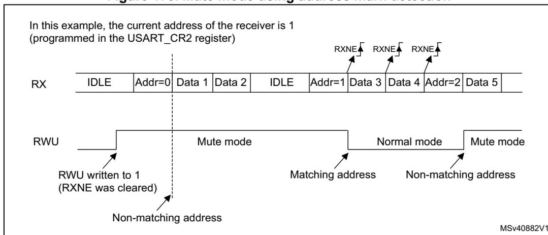
The diagram shows the RX signal and RWU signal. The RX signal contains IDLE, Addr=0, Data 1, Data 2, IDLE, Addr=1, Data 3, Data 4, Addr=2, and Data 5. The RWU signal is initially low. When RWU is written to 1 (RXNE was cleared), the USART enters Mute mode. Upon receiving Addr=0 (a non-matching address), the USART stays in Mute mode. Upon receiving Addr=1 (a matching address), the USART exits Mute mode and enters Normal mode. Upon receiving Addr=2 (a non-matching address), the USART enters Mute mode again. The RXNE flag is set for Data 1, Data 2, Data 3, Data 4, and Data 5 in Normal mode.
19.3.7 Parity control
Parity control (generation of parity bit in transmission and parity checking in reception) can be enabled by setting the PCE bit in the USART_CR1 register. Depending on the frame length defined by the M bit, the possible USART frame formats are as listed in Table 85 .
Table 85. Frame formats
| M bit | PCE bit | USART frame (1) |
|---|---|---|
| 0 | 0 | | SB | 8 bit data | STB | |
| 0 | 1 | | SB | 7-bit data | PB | STB | |
| 1 | 0 | | SB | 9-bit data | STB | |
| 1 | 1 | | SB | 8-bit data PB | STB | |
1. Legends: SB: start bit, STB: stop bit, PB: parity bit.
Even parity
The parity bit is calculated to obtain an even number of “1s” inside the frame made of the 7 or 8 LSB bits (depending on whether M is equal to 0 or 1) and the parity bit.
E.g.: data=00110101; 4 bits set => parity bit is 0 if even parity is selected (PS bit in USART_CR1 = 0).
Odd parity
The parity bit is calculated to obtain an odd number of “1s” inside the frame made of the 7 or 8 LSB bits (depending on whether M is equal to 0 or 1) and the parity bit.
E.g.: data=00110101; 4 bits set => parity bit is 1 if odd parity is selected (PS bit in USART_CR1 = 1).
Parity checking in reception
If the parity check fails, the PE flag is set in the USART_SR register and an interrupt is generated if PEIE is set in the USART_CR1 register. The PE flag is cleared by a software sequence (a read from the status register followed by a read or write access to the USART_DR data register).
Note: In case of wake-up by an address mark: the MSB bit of the data is taken into account to identify an address but not the parity bit. And the receiver does not check the parity of the address data (PE is not set in case of a parity error).
Parity generation in transmission
If the PCE bit is set in USART_CR1, then the MSB bit of the data written in the data register is transmitted but is changed by the parity bit (even number of “1s” if even parity is selected (PS=0) or an odd number of “1s” if odd parity is selected (PS=1)).
Note: The software routine that manages the transmission can activate the software sequence which clears the PE flag (a read from the status register followed by a read or write access to the data register). When operating in half-duplex mode, depending on the software, this can cause the PE flag to be unexpectedly cleared.
19.3.8 LIN (local interconnection network) mode
The LIN mode is selected by setting the LINEN bit in the USART_CR2 register. In LIN mode, the following bits must be kept cleared:
- • STOP[1:0] and CLKEN in the USART_CR2 register
- • SCEN, HDSEL and IREN in the USART_CR3 register.
LIN transmission
The same procedure explained in Section 19.3.2 has to be applied for LIN Master transmission than for normal USART transmission with the following differences:
- • Clear the M bit to configure 8-bit word length.
- • Set the LINEN bit to enter LIN mode. In this case, setting the SBK bit sends 13 '0 bits as a break character. Then a bit of value '1 is sent to allow the next start detection.
LIN reception
A break detection circuit is implemented on the USART interface. The detection is totally independent from the normal USART receiver. A break can be detected whenever it occurs, during Idle state or during a frame.
When the receiver is enabled (RE=1 in USART_CR1), the circuit looks at the RX input for a start signal. The method for detecting start bits is the same when searching break characters or data. After a start bit has been detected, the circuit samples the next bits exactly like for the data (on the 8th, 9th and 10th samples). If 10 (when the LBDL = 0 in USART_CR2) or 11 (when LBDL=1 in USART_CR2) consecutive bits are detected as '0, and are followed by a delimiter character, the LBD flag is set in USART_SR. If the LBDIE bit=1, an interrupt is generated. Before validating the break, the delimiter is checked for as it signifies that the RX line has returned to a high level.
If a '1 is sampled before the 10 or 11 have occurred, the break detection circuit cancels the current detection and searches for a start bit again.
If the LIN mode is disabled (LINEN=0), the receiver continues working as normal USART, without taking into account the break detection.
If the LIN mode is enabled (LINEN=1), as soon as a framing error occurs (stop bit detected at '0, which is the case for any break frame), the receiver stops until the break detection circuit receives either a '1, if the break word was not complete, or a delimiter character if a break has been detected.
The behavior of the break detector state machine and the break flag is shown on the Figure 176: Break detection in LIN mode (11-bit break length - LBDL bit is set) on page 530 .
Examples of break frames are given on Figure 177: Break detection in LIN mode vs. Framing error detection on page 531 .
Figure 176. Break detection in LIN mode (11-bit break length - LBDL bit is set)
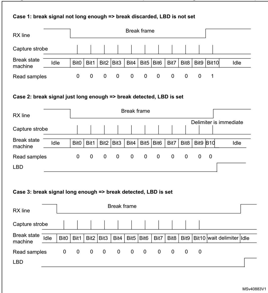
Case 1: break signal not long enough => break discarded, LBD is not set
RX line: Break frame
Capture strobe
| Break state machine | Idle | Bit0 | Bit1 | Bit2 | Bit3 | Bit4 | Bit5 | Bit6 | Bit7 | Bit8 | Bit9 | Bit10 | Idle |
| Read samples | 0 | 0 | 0 | 0 | 0 | 0 | 0 | 0 | 0 | 0 | 1 |
Case 2: break signal just long enough => break detected, LBD is set
RX line: Break frame
Capture strobe
Delimiter is immediate
| Break state machine | Idle | Bit0 | Bit1 | Bit2 | Bit3 | Bit4 | Bit5 | Bit6 | Bit7 | Bit8 | Bit9 | Bit10 | Idle |
| Read samples | 0 | 0 | 0 | 0 | 0 | 0 | 0 | 0 | 0 | 0 | 0 |
LBD
Case 3: break signal long enough => break detected, LBD is set
RX line: Break frame
Capture strobe
| Break state machine | Idle | Bit0 | Bit1 | Bit2 | Bit3 | Bit4 | Bit5 | Bit6 | Bit7 | Bit8 | Bit9 | Bit10 | wait delimiter | Idle |
| Read samples | 0 | 0 | 0 | 0 | 0 | 0 | 0 | 0 | 0 | 0 | 0 |
LBD
MSv40883V1
Figure 177. Break detection in LIN mode vs. Framing error detection
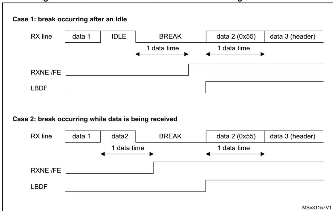
Case 1: break occurring after an Idle
The diagram shows the RX line transitioning from IDLE to BREAK, then to data 2 (0x55) and data 3 (header). The RXNE/FE signal is shown as a step function that goes high when the line is in BREAK and returns low when it is in IDLE. The LBDF signal is shown as a step function that goes high when the line is in BREAK and returns low when it is in IDLE. The time between the start of the BREAK and the start of data 2 is labeled as 1 data time. The time between the start of data 2 and the start of data 3 is also labeled as 1 data time.
Case 2: break occurring while data is being received
The diagram shows the RX line transitioning from data 1 to data 2, then to BREAK, then to data 2 (0x55) and data 3 (header). The RXNE/FE signal is shown as a step function that goes high when the line is in BREAK and returns low when it is in IDLE. The LBDF signal is shown as a step function that goes high when the line is in BREAK and returns low when it is in IDLE. The time between the start of data 2 and the start of the BREAK is labeled as 1 data time. The time between the start of the BREAK and the start of data 2 (0x55) is also labeled as 1 data time.
MSv31157V1
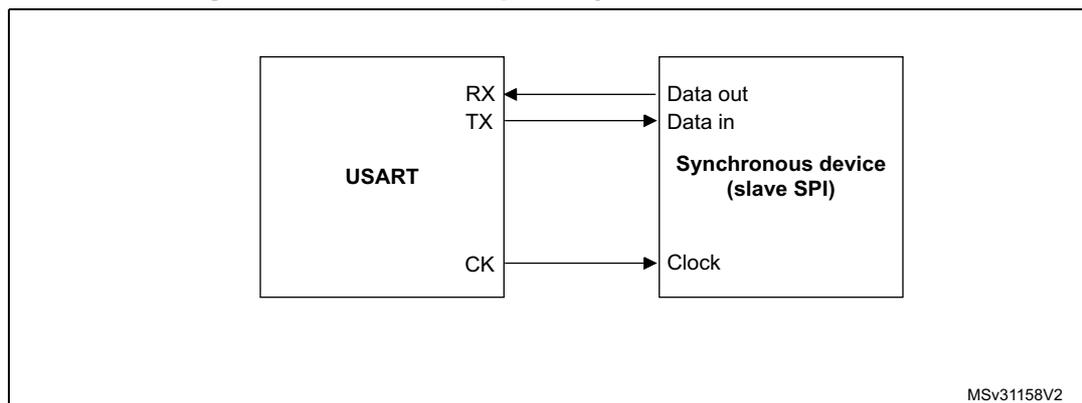
19.3.9 USART synchronous mode
The synchronous mode is selected by writing the CLKEN bit in the USART_CR2 register to 1. In synchronous mode, the following bits must be kept cleared:
- • LINEN bit in the USART_CR2 register,
- • SCEN, HDSEL and IREN bits in the USART_CR3 register.
The USART allows the user to control a bidirectional synchronous serial communications in master mode. The CK pin is the output of the USART transmitter clock. No clock pulses are sent to the CK pin during start bit and stop bit. Depending on the state of the LBCL bit in the USART_CR2 register clock pulses are generated or not during the last valid data bit (address mark). The CPOL bit in the USART_CR2 register allows the user to select the clock polarity, and the CPHA bit in the USART_CR2 register allows the user to select the phase of the external clock (see Figure 178 , Figure 179 & Figure 180 ).
During the Idle state, preamble and send break, the external CK clock is not activated.
In synchronous mode the USART transmitter works exactly like in asynchronous mode. But as CK is synchronized with TX (according to CPOL and CPHA), the data on TX is synchronous.
In this mode the USART receiver works in a different manner compared to the asynchronous mode. If RE=1, the data is sampled on CK (rising or falling edge, depending on CPOL and CPHA), without any oversampling. A setup and a hold time must be respected (which depends on the baud rate: 1/16 bit time).
Note: The CK pin works in conjunction with the TX pin. Thus, the clock is provided only if the transmitter is enabled (TE=1) and a data is being transmitted (the data register USART_DR
has been written). This means that it is not possible to receive a synchronous data without transmitting data.
The LBCL, CPOL and CPHA bits have to be selected when both the transmitter and the receiver are disabled (TE=RE=0) to ensure that the clock pulses function correctly. These bits should not be changed while the transmitter or the receiver is enabled.
It is advised that TE and RE are set in the same instruction in order to minimize the setup and the hold time of the receiver.
The USART supports master mode only: it cannot receive or send data related to an input clock (CK is always an output).
Figure 178. USART example of synchronous transmission
MSv31158V2
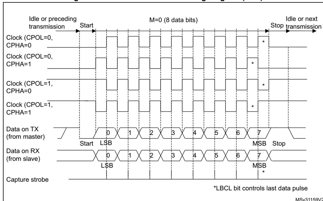
Figure 179. USART data clock timing diagram (M=0)
MSv31159V2
*LBCL bit controls last data pulse
Figure 180. USART data clock timing diagram (M=1)
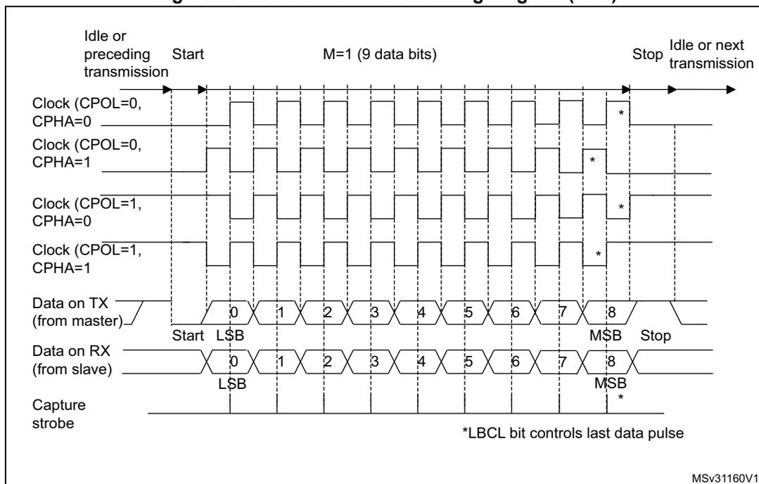
Idle or preceding transmission Start M=1 (9 data bits) Stop Idle or next transmission
Clock (CPOL=0, CPHA=0)
Clock (CPOL=0, CPHA=1)
Clock (CPOL=1, CPHA=0)
Clock (CPOL=1, CPHA=1)
Data on TX (from master) Start LSB 0 1 2 3 4 5 6 7 8 MSB Stop
Data on RX (from slave) Start LSB 0 1 2 3 4 5 6 7 8 MSB Stop
Capture strobe
*LBCL bit controls last data pulse
MSV31160V1
Figure 181. RX data setup/hold time
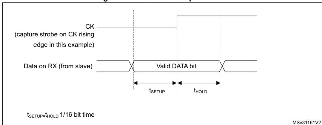
CK (capture strobe on CK rising edge in this example)
Data on RX (from slave)
Valid DATA bit
\( t_{SETUP} \) \( t_{HOLD} \)
\( t_{SETUP} = t_{HOLD} = 1/16 \) bit time
MSV31161V2
Note: The function of CK is different in Smartcard mode. Refer to the Smartcard mode chapter for more details.
19.3.10 Single-wire half-duplex communication
The single-wire half-duplex mode is selected by setting the HDSEL bit in the USART_CR3 register. In this mode, the following bits must be kept cleared:
- • LINEN and CLKEN bits in the USART_CR2 register,
- • SCEN and IREN bits in the USART_CR3 register.
The USART can be configured to follow a single-wire half-duplex protocol where the TX and RX lines are internally connected. The selection between half- and full-duplex communication is made with a control bit ‘HALF DUPLEX SEL’ (HDSEL in USART_CR3).
As soon as HDSEL is written to 1:
- • the TX and RX lines are internally connected
- • the RX pin is no longer used
- • the TX pin is always released when no data is transmitted. Thus, it acts as a standard I/O in idle or in reception. It means that the I/O must be configured so that TX is configured as floating input (or output high open-drain) when not driven by the USART.
Apart from this, the communications are similar to what is done in normal USART mode. The conflicts on the line must be managed by the software (by the use of a centralized arbiter, for instance). In particular, the transmission is never blocked by hardware and continue to occur as soon as a data is written in the data register while the TE bit is set.
19.3.11 Smartcard
The Smartcard mode is selected by setting the SCEN bit in the USART_CR3 register. In smartcard mode, the following bits must be kept cleared:
- • LINEN bit in the USART_CR2 register,
- • HDSEL and IREN bits in the USART_CR3 register.
Moreover, the CLKEN bit may be set in order to provide a clock to the smartcard.
The Smartcard interface is designed to support asynchronous protocol Smartcards as defined in the ISO 7816-3 standard. The USART should be configured as:
- • 8 bits plus parity: where M=1 and PCE=1 in the USART_CR1 register
- • 1.5 stop bits when transmitting and receiving: where STOP=11 in the USART_CR2 register.
Note: It is also possible to choose 0.5 stop bit for receiving but it is recommended to use 1.5 stop bits for both transmitting and receiving to avoid switching between the two configurations.
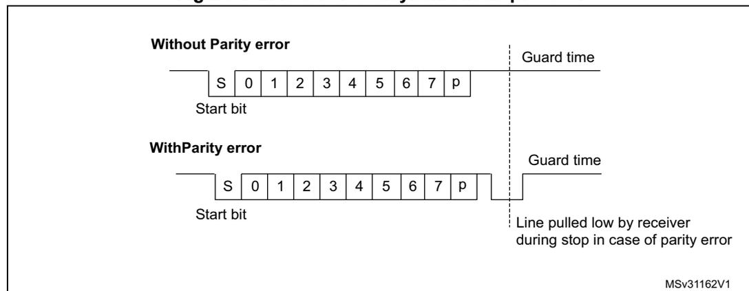
Figure 182 shows examples of what can be seen on the data line with and without parity error.
Figure 182. ISO 7816-3 asynchronous protocol
When connected to a Smartcard, the TX output of the USART drives a bidirectional line that is also driven by the Smartcard. The TX pin must be configured as open-drain.
Smartcard is a single wire half duplex communication protocol.
- • Transmission of data from the transmit shift register is guaranteed to be delayed by a minimum of 1/2 baud clock. In normal operation a full transmit shift register starts
shifting on the next baud clock edge. In Smartcard mode this transmission is further delayed by a guaranteed 1/2 baud clock.
- • If a parity error is detected during reception of a frame programmed with a 0.5 or 1.5 stop bit period, the transmit line is pulled low for a baud clock period after the completion of the receive frame. This is to indicate to the Smartcard that the data transmitted to USART has not been correctly received. This NACK signal (pulling transmit line low for 1 baud clock) causes a framing error on the transmitter side (configured with 1.5 stop bits). The application can handle re-sending of data according to the protocol. A parity error is 'NACK'ed by the receiver if the NACK control bit is set, otherwise a NACK is not transmitted.
- • The assertion of the TC flag can be delayed by programming the Guard Time register. In normal operation, TC is asserted when the transmit shift register is empty and no further transmit requests are outstanding. In Smartcard mode an empty transmit shift register triggers the guard time counter to count up to the programmed value in the Guard Time register. TC is forced low during this time. When the guard time counter reaches the programmed value TC is asserted high.
- • The de-assertion of TC flag is unaffected by Smartcard mode.
- • If a framing error is detected on the transmitter end (due to a NACK from the receiver), the NACK is not detected as a start bit by the receive block of the transmitter. According to the ISO protocol, the duration of the received NACK can be 1 or 2 baud clock periods.
- • On the receiver side, if a parity error is detected and a NACK is transmitted the receiver does not detect the NACK as a start bit.
Note: A break character is not significant in Smartcard mode. A 0x00 data with a framing error is treated as data and not as a break.
No Idle frame is transmitted when toggling the TE bit. The Idle frame (as defined for the other configurations) is not defined by the ISO protocol.
Figure 183 details how the NACK signal is sampled by the USART. In this example the USART is transmitting a data and is configured with 1.5 stop bits. The receiver part of the USART is enabled in order to check the integrity of the data and the NACK signal.
Figure 183. Parity error detection using the 1.5 stop bits
The diagram illustrates the timing for parity error detection with 1.5 stop bits. It shows two horizontal lines representing signal levels. The top line represents the transmitted signal, and the bottom line represents the received signal. The transmitted signal is divided into three segments: Bit 7 (1 bit time), Parity bit (1 bit time), and 1.5 Stop bit (1.5 bit times). The Stop bit is further divided into two 0.5 bit time segments. The received signal shows sampling points at the 8th, 9th, and 10th bit times for both the Parity bit and the Stop bit. The diagram indicates that the receiver samples the Parity bit and the first 0.5 bit time of the Stop bit, while the second 0.5 bit time of the Stop bit is ignored. The label 'MSv31163V1' is present in the bottom right corner of the diagram.
The USART can provide a clock to the smartcard through the CK output. In smartcard mode, CK is not associated to the communication but is simply derived from the internal peripheral input clock through a 5-bit prescaler. The division ratio is configured in the
prescaler register USART_GTPR. CK frequency can be programmed from \( f_{CK}/2 \) to \( f_{CK}/62 \) , where \( f_{CK} \) is the peripheral input clock.
19.3.12 IrDA SIR ENDEC block
The IrDA mode is selected by setting the IREN bit in the USART_CR3 register. In IrDA mode, the following bits must be kept cleared:
- • LINEN, STOP and CLKEN bits in the USART_CR2 register,
- • SCEN and HDSEL bits in the USART_CR3 register.
The IrDA SIR physical layer specifies use of a Return to Zero, Inverted (RZI) modulation scheme that represents logic 0 as an infrared light pulse (see Figure 184 ).
The SIR Transmit encoder modulates the Non Return to Zero (NRZ) transmit bit stream output from USART. The output pulse stream is transmitted to an external output driver and infrared LED. USART supports only bit rates up to 115.2Kbps for the SIR ENDEC. In normal mode the transmitted pulse width is specified as 3/16 of a bit period.
The SIR receive decoder demodulates the return-to-zero bit stream from the infrared detector and outputs the received NRZ serial bit stream to USART. The decoder input is normally HIGH (marking state) in the Idle state. The transmit encoder output has the opposite polarity to the decoder input. A start bit is detected when the decoder input is low.
- • IrDA is a half duplex communication protocol. If the Transmitter is busy (i.e. the USART is sending data to the IrDA encoder), any data on the IrDA receive line is ignored by the IrDA decoder and if the Receiver is busy (USART is receiving decoded data from the USART), data on the TX from the USART to IrDA is not encoded by IrDA. While receiving data, transmission should be avoided as the data to be transmitted could be corrupted.
- • A '0' is transmitted as a high pulse and a '1' is transmitted as a '0'. The width of the pulse is specified as 3/16th of the selected bit period in normal mode (see Figure 185 ).
- • The SIR decoder converts the IrDA compliant receive signal into a bit stream for USART.
- • The SIR receive logic interprets a high state as a logic one and low pulses as logic zeros.
- • The transmit encoder output has the opposite polarity to the decoder input. The SIR output is in low state when Idle.
- • The IrDA specification requires the acceptance of pulses greater than 1.41 us. The acceptable pulse width is programmable. Glitch detection logic on the receiver end filters out pulses of width less than 2 PSC periods (PSC is the prescaler value programmed in the IrDA low-power Baud Register, USART_GTPR). Pulses of width less than 1 PSC period are always rejected, but those of width greater than one and less than two periods may be accepted or rejected, those greater than 2 periods are accepted as a pulse. The IrDA encoder/decoder does not work when PSC = 0.
- • The receiver can communicate with a low-power transmitter.
- • In IrDA mode, the STOP bits in the USART_CR2 register must be configured to "1 stop bit".
IrDA low-power mode
Transmitter:
In low-power mode the pulse width is not maintained at 3/16 of the bit period. Instead, the width of the pulse is 3 times the low-power baud rate which can be a minimum of 1.42 MHz. Generally this value is 1.8432 MHz ( \( 1.42\text{ MHz} < \text{PSC} < 2.12\text{ MHz} \) ). A low-power mode programmable divisor divides the system clock to achieve this value.
Receiver:
Receiving in low-power mode is similar to receiving in normal mode. For glitch detection the USART should discard pulses of duration shorter than \( 1/\text{PSC} \) . A valid low is accepted only if its duration is greater than 2 periods of the IrDA low-power Baud clock (PSC value in USART_GTPR).
Note:
A pulse of width less than two and greater than one PSC period(s) may or may not be rejected.
The receiver set up time should be managed by software. The IrDA physical layer specification specifies a minimum of 10 ms delay between transmission and reception (IrDA is a half duplex protocol).
Figure 184. IrDA SIR ENDEC- block diagram
Figure 185. IrDA data modulation (3/16) -Normal mode
19.3.13 Continuous communication using DMA
The USART is capable of continuous communication using the DMA. The DMA requests for Rx buffer and Tx buffer are generated independently.
Transmission using DMA
DMA mode can be enabled for transmission by setting DMAT bit in the USART_CR3 register. Data is loaded from a SRAM area configured using the DMA peripheral (refer to the DMA specification) to the USART_DR register whenever the TXE bit is set. To map a DMA channel for USART transmission, use the following procedure (x denotes the channel number):
- 1. Write the USART_DR register address in the DMA control register to configure it as the destination of the transfer. The data are moved to this address from memory after each TXE event.
- 2. Write the memory address in the DMA control register to configure it as the source of the transfer. The data are loaded into the USART_DR register from this memory area after each TXE event.
- 3. Configure the total number of bytes to be transferred to the DMA control register.
- 4. Configure the channel priority in the DMA register
- 5. Configure DMA interrupt generation after half/ full transfer as required by the application.
- 6. Clear the TC bit in the SR register by writing 0 to it.
- 7. Activate the channel in the DMA register.
When the number of data transfers programmed in the DMA Controller is reached, the DMA controller generates an interrupt on the DMA channel interrupt vector.
In transmission mode, once the DMA has written all the data to be transmitted (the TCIF flag is set in the DMA_ISR register), the TC flag can be monitored to make sure that the USART communication is complete. This is required to avoid corrupting the last transmission before disabling the USART or entering the Stop mode. The software must wait until TC=1. The TC flag remains cleared during all data transfers and it is set by hardware at the last frame's end of transmission.
Figure 186. Transmission using DMA
The diagram illustrates the timing and sequence of events for USART transmission using DMA. The TX line shows an idle preamble followed by three frames (F1, F2, F3). The TXE flag is set by hardware and cleared by DMA read. The DMA request is set by hardware and ignored by the DMA because the DMA transfer is complete. The USART_DR register contains F1, F2, and F3. The TC flag is set by hardware and clear by software. The DMA writes are shown as F1, F2, and F3 into the USART_DR register. The DMA TCIF (Transfer complete) flag is set by hardware and clear by software. The software configures the DMA to send 3 data and enables the USART. The DMA writes F1 into USART_DR, F2 into USART_DR, and F3 into USART_DR. The DMA transfer is complete (TCIF=1 in DMA_ISR). The software waits until TC=1.
Reception using DMA
DMA mode can be enabled for reception by setting the DMAR bit in USART_CR3 register. Data is loaded from the USART_DR register to a SRAM area configured using the DMA peripheral (refer to the DMA specification) whenever a data byte is received. To map a DMA channel for USART reception, use the following procedure:
- 1. Write the USART_DR register address in the DMA control register to configure it as the source of the transfer. The data are moved from this address to the memory after each RXNE event.
- 2. Write the memory address in the DMA control register to configure it as the destination of the transfer. The data are loaded from USART_DR to this memory area after each RXNE event.
- 3. Configure the total number of bytes to be transferred in the DMA control register.
- 4. Configure the channel priority in the DMA control register
- 5. Configure interrupt generation after half/ full transfer as required by the application.
- 6. Activate the channel in the DMA control register.
When the number of data transfers programmed in the DMA Controller is reached, the DMA controller generates an interrupt on the DMA channel interrupt vector. The DMAR bit should be cleared by software in the USART_CR3 register during the interrupt subroutine.
Figure 187. Reception using DMA
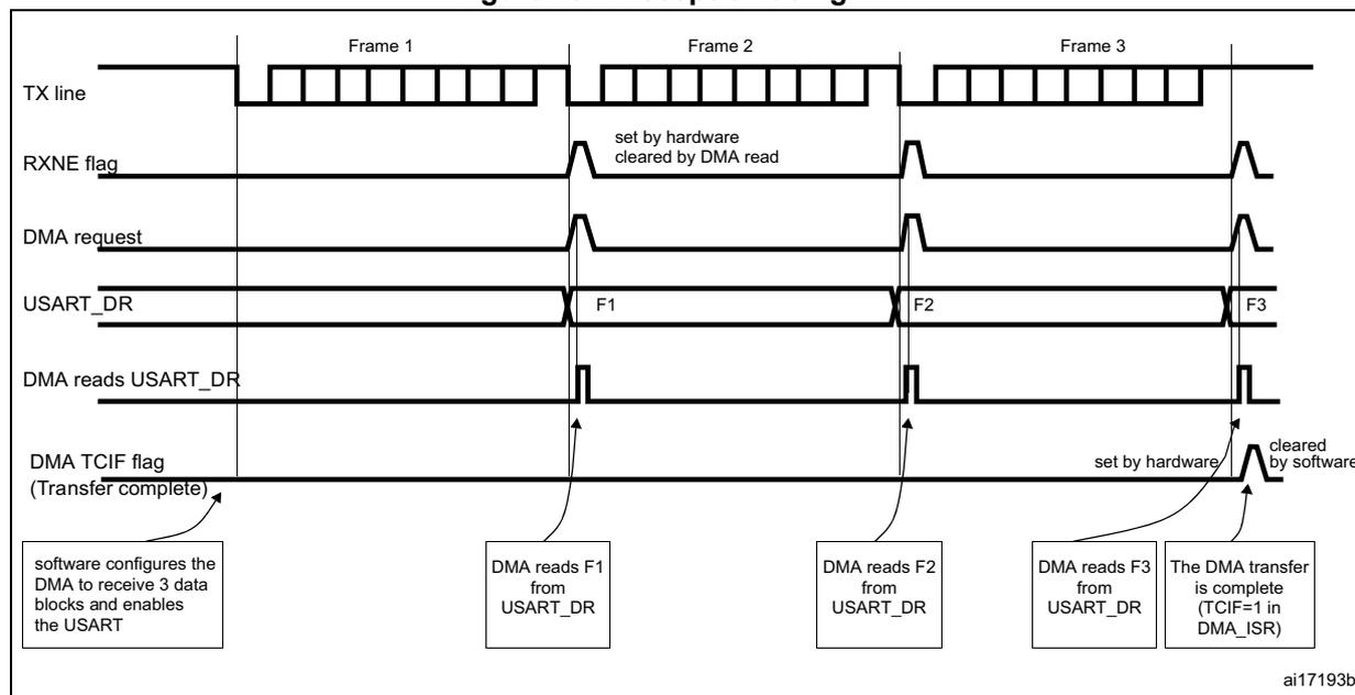
Error flagging and interrupt generation in multibuffer communication
In case of multibuffer communication if any error occurs during the transaction the error flag is asserted after the current byte. An interrupt is generated if the interrupt enable flag is set. For framing error, overrun error and noise flag which are asserted with RXNE in case of single byte reception, there is a separate error flag interrupt enable bit (EIE bit in the USART_CR3 register), which if set, issues an interrupt after the current byte with either of these errors.
19.3.14 Hardware flow control
It is possible to control the serial data flow between 2 devices by using the CTS input and the RTS output. The Figure 188 shows how to connect 2 devices in this mode:
Figure 188. Hardware flow control between 2 USARTs
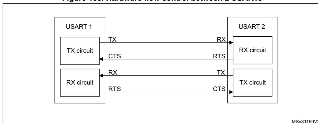
RTS and CTS flow control can be enabled independently by writing respectively RTSE and CTSE bits to 1 (in the USART_CR3 register).
RTS flow control
If the RTS flow control is enabled (RTSE=1), then RTS is asserted (tied low) as long as the USART receiver is ready to receive a new data. When the receive register is full, RTS is deasserted, indicating that the transmission is expected to stop at the end of the current frame. Figure 189 shows an example of communication with RTS flow control enabled.
Figure 189. RTS flow control
The diagram illustrates the relationship between the RX (receive) signal and the RTS (Request To Send) signal during two data transmissions. The RX signal shows two frames: the first contains 'Start bit', 'Data 1', and 'Stop bit'; the second contains 'Start bit', 'Data 2', and 'Stop bit'. Vertical dashed lines mark the start and end of each frame, with an 'Idle' period between them. The RTS signal is initially high. It drops to low at the start of the first frame (marked by RXNE↑). It returns to high at the end of the first frame (marked by RXNE↓). It drops to low again at the start of the second frame (marked by RXNE↑). It returns to high at the end of the second frame (marked by RXNE↓). Between the two frames, a label indicates 'Data 1 read' and 'Data 2 can now be transmitted'.
CTS flow control
If the CTS flow control is enabled (CTSE=1), then the transmitter checks the CTS input before transmitting the next frame. If CTS is asserted (tied low), then the next data is transmitted (assuming that a data is to be transmitted, in other words, if TXE=0), else the transmission does not occur. When CTS is deasserted during a transmission, the current transmission is completed before the transmitter stops.
When CTSE=1, the CTSIF status bit is automatically set by hardware as soon as the CTS input toggles. It indicates when the receiver becomes ready or not ready for communication. An interrupt is generated if the CTSIE bit in the USART_CR3 register is set. The figure below shows an example of communication with CTS flow control enabled.
Figure 190. CTS flow control
The diagram illustrates the CTS flow control mechanism across three horizontal timelines:
- CTS: The Clear To Send signal. It starts high, goes low when Data 2 is being transmitted, and returns high after Data 2 is finished. It goes low again when Data 3 is written to the TDR and returns high after Data 3 is transmitted.
- Transmit data register (TDR): Shows the data to be transmitted. It contains 'Data 2', then becomes 'empty', then contains 'Data 3', and finally becomes 'empty' again.
- TX: The actual transmission line. It shows the sequence: 'Data 1' (Stop bit, Start bit, Data 2, Stop bit), followed by an 'Idle' state, then 'Data 3' (Stop bit, Start bit, Data 3, Stop bit).
Key events and annotations:
- An arrow labeled "Writing data 3 in TDR" points to the moment 'Data 3' is written to the register, which occurs while 'Data 2' is still being transmitted and the CTS signal is high.
- An arrow labeled "Transmission of Data 3 is delayed until CTS = 0" points to the start of the 'Data 3' transmission sequence on the TX line, which only begins after the CTS signal has gone low.
- Vertical dashed lines mark the boundaries between different data transmissions and register states.
- The diagram is labeled with "MSV68793V1" in the bottom right corner.
Note: Special behavior of break frames: when the CTS flow is enabled, the transmitter does not check the CTS input state to send a break.
19.4 USART interrupts
Table 86. USART interrupt requests
| Interrupt event | Event flag | Enable control bit |
|---|---|---|
| Transmit Data Register Empty | TXE | TXEIE |
| CTS flag | CTS | CTSIE |
| Transmission Complete | TC | TCIE |
| Received Data Ready to be Read | RXNE | RXNEIE |
| Overrun Error Detected | ORE | |
| Idle Line Detected | IDLE | IDLEIE |
| Parity Error | PE | PEIE |
| Break Flag | LBD | LBDIE |
| Noise Flag, Overrun error and Framing Error in multibuffer communication | NF or ORE or FE | EIE |
The USART interrupt events are connected to the same interrupt vector (see Figure 191 ).
- • During transmission: Transmission Complete, Clear to Send or Transmit Data Register empty interrupt.
- • While receiving: Idle Line detection, Overrun error, Receive Data register not empty, Parity error, LIN break detection, Noise Flag (only in multi buffer communication) and Framing Error (only in multi buffer communication).
These events generate an interrupt if the corresponding Enable Control Bit is set.
Figure 191. USART interrupt mapping diagram
19.5 USART mode configuration
Table 87. USART mode configuration (1)
| USART modes | USART1 | USART2 | USART6 |
|---|---|---|---|
| Asynchronous mode | X | X | X |
| Hardware flow control | X | X | X |
| Multibuffer communication (DMA) | X | X | X |
| Multiprocessor communication | X | X | X |
| Synchronous | X | X | X |
| Smartcard | X | X | X |
| Half-duplex (single-wire mode) | X | X | X |
| IrDA | X | X | X |
| LIN | X | X | X |
1. X = supported; NA = not applicable.
19.6 USART registers
Refer to Section 1.1: List of abbreviations for registers for registers for a list of abbreviations used in register descriptions.
The peripheral registers have to be accessed by half-words (16 bits) or words (32 bits).
19.6.1 Status register (USART_SR)
Address offset: 0x00
Reset value: 0x00C0 0000
| 31 | 30 | 29 | 28 | 27 | 26 | 25 | 24 | 23 | 22 | 21 | 20 | 19 | 18 | 17 | 16 |
|---|---|---|---|---|---|---|---|---|---|---|---|---|---|---|---|
| Reserved | |||||||||||||||
| 15 | 14 | 13 | 12 | 11 | 10 | 9 | 8 | 7 | 6 | 5 | 4 | 3 | 2 | 1 | 0 |
| Reserved | CTS | LBD | TXE | TC | RXNE | IDLE | ORE | NF | FE | ||||||
| rc_w0 | rc_w0 | r | rc_w0 | rc_w0 | r | r | r | r | |||||||
Bits 31:10 Reserved, must be kept at reset value
Bit 9 CTS : CTS flag
This bit is set by hardware when the CTS input toggles, if the CTSE bit is set. It is cleared by software (by writing it to 0). An interrupt is generated if CTSIE=1 in the USART_CR3 register.
Note:
0: No change occurred on the CTS status line
1: A change occurred on the CTS status line
Bit 8 LBD : LIN break detection flag
This bit is set by hardware when the LIN break is detected. It is cleared by software (by writing it to 0). An interrupt is generated if LBDIE = 1 in the USART_CR2 register.
0: LIN Break not detected
1: LIN break detected
Note: An interrupt is generated when LBD=1 if LBDIE=1
Bit 7 TXE: Transmit data register emptyThis bit is set by hardware when the content of the TDR register has been transferred into the shift register. An interrupt is generated if the TXEIE bit =1 in the USART_CR1 register. It is cleared by a write to the USART_DR register.
0: Data is not transferred to the shift register
1: Data is transferred to the shift register)
Note: This bit is used during single buffer transmission.
Bit 6 TC: Transmission completeThis bit is set by hardware if the transmission of a frame containing data is complete and if TXE is set. An interrupt is generated if TCIE=1 in the USART_CR1 register. It is cleared by a software sequence (a read from the USART_SR register followed by a write to the USART_DR register). The TC bit can also be cleared by writing a '0' to it. This clearing sequence is recommended only for multibuffer communication.
0: Transmission is not complete
1: Transmission is complete
Bit 5 RXNE: Read data register not emptyThis bit is set by hardware when the content of the RDR shift register has been transferred to the USART_DR register. An interrupt is generated if RXNEIE=1 in the USART_CR1 register. It is cleared by a read to the USART_DR register. The RXNE flag can also be cleared by writing a zero to it. This clearing sequence is recommended only for multibuffer communication.
0: Data is not received
1: Received data is ready to be read.
Bit 4 IDLE: IDLE line detectedThis bit is set by hardware when an Idle Line is detected. An interrupt is generated if the IDLEIE=1 in the USART_CR1 register. It is cleared by a software sequence (an read to the USART_SR register followed by a read to the USART_DR register).
0: No Idle Line is detected
1: Idle Line is detected
Note: The IDLE bit is not set again until the RXNE bit has been set itself (a new idle line occurs).
Bit 3 ORE: Overrun errorThis bit is set by hardware when the word currently being received in the shift register is ready to be transferred into the RDR register while RXNE=1. An interrupt is generated if RXNEIE=1 in the USART_CR1 register. It is cleared by a software sequence (an read to the USART_SR register followed by a read to the USART_DR register).
0: No Overrun error
1: Overrun error is detected
Note: When this bit is set, the RDR register content is not lost but the shift register is overwritten. An interrupt is generated on ORE flag in case of Multi Buffer communication if the EIE bit is set.
Bit 2 NF: Noise detected flagThis bit is set by hardware when noise is detected on a received frame. It is cleared by a software sequence (an read to the USART_SR register followed by a read to the USART_DR register).
0: No noise is detected
1: Noise is detected
Note: This bit does not generate interrupt as it appears at the same time as the RXNE bit which itself generates an interrupting interrupt is generated on NF flag in case of Multi Buffer communication if the EIE bit is set.
Note: When the line is noise-free, the NF flag can be disabled by programming the ONEBIT bit to 1 to increase the USART tolerance to deviations (Refer to Section 19.3.5: USART receiver tolerance to clock deviation on page 525 ).
Bit 1 FE: Framing errorThis bit is set by hardware when a de-synchronization, excessive noise or a break character is detected. It is cleared by a software sequence (an read to the USART_SR register followed by a read to the USART_DR register).
0: No Framing error is detected
1: Framing error or break character is detected
Note: This bit does not generate interrupt as it appears at the same time as the RXNE bit which itself generates an interrupt. If the word currently being transferred causes both frame error and overrun error, it is transferred and only the ORE bit is set.
An interrupt is generated on FE flag in case of Multi Buffer communication if the EIE bit is set.
Bit 0 PE: Parity errorThis bit is set by hardware when a parity error occurs in receiver mode. It is cleared by a software sequence (a read from the status register followed by a read or write access to the USART_DR data register). The software must wait for the RXNE flag to be set before clearing the PE bit.
An interrupt is generated if PEIE = 1 in the USART_CR1 register.
0: No parity error
1: Parity error
19.6.2 Data register (USART_DR)
Address offset: 0x04
Reset value: 0xXXXX XXXX
Bits 31:9 Reserved, must be kept at reset value
Bits 8:0 DR[8:0] : Data value
Contains the Received or Transmitted data character, depending on whether it is read from or written to.
The Data register performs a double function (read and write) since it is composed of two registers, one for transmission (TDR) and one for reception (RDR)
The TDR register provides the parallel interface between the internal bus and the output shift register (see Figure 167: USART block diagram ).
The RDR register provides the parallel interface between the input shift register and the internal bus.
When transmitting with the parity enabled (PCE bit set to 1 in the USART_CR1 register), the value written in the MSB (bit 7 or bit 8 depending on the data length) has no effect because it is replaced by the parity.
When receiving with the parity enabled, the value read in the MSB bit is the received parity bit.
19.6.3 Baud rate register (USART_BRR)
Note: The baud counters stop counting if the TE or RE bits are disabled respectively.
Address offset: 0x08
Reset value: 0x0000 0000
| 31 | 30 | 29 | 28 | 27 | 26 | 25 | 24 | 23 | 22 | 21 | 20 | 19 | 18 | 17 | 16 |
|---|---|---|---|---|---|---|---|---|---|---|---|---|---|---|---|
| Reserved | |||||||||||||||
| 15 | 14 | 13 | 12 | 11 | 10 | 9 | 8 | 7 | 6 | 5 | 4 | 3 | 2 | 1 | 0 |
| DIV_Mantissa[11:0] | DIV_Fraction[3:0] | ||||||||||||||
| rw | rw | rw | rw | rw | rw | rw | rw | rw | rw | rw | rw | rw | rw | rw | rw |
Bits 31:16 Reserved, must be kept at reset value
Bits 15:4 DIV_Mantissa[11:0] : mantissa of USARTDIV
These 12 bits define the mantissa of the USART Divider (USARTDIV)
Bits 3:0 DIV_Fraction[3:0] : fraction of USARTDIV
These 4 bits define the fraction of the USART Divider (USARTDIV). When OVER8=1, the DIV_Fraction3 bit is not considered and must be kept cleared.
19.6.4 Control register 1 (USART_CR1)
Address offset: 0x0C
Reset value: 0x0000 0000
| 31 | 30 | 29 | 28 | 27 | 26 | 25 | 24 | 23 | 22 | 21 | 20 | 19 | 18 | 17 | 16 |
|---|---|---|---|---|---|---|---|---|---|---|---|---|---|---|---|
| Reserved | |||||||||||||||
| 15 | 14 | 13 | 12 | 11 | 10 | 9 | 8 | 7 | 6 | 5 | 4 | 3 | 2 | 1 | 0 |
| OVER8 | Reserved | UE | M | WAKE | PCE | PS | PEIE | TXEIE | TCIE | RXNEIE | IDLEIE | TE | RE | RWU | SBK |
| rw | Res. | rw | rw | rw | rw | rw | rw | rw | rw | rw | rw | rw | rw | rw | rw |
Bits 31:16 Reserved, must be kept at reset value
Bit 15 OVER8 : Oversampling mode
0: oversampling by 16
1: oversampling by 8
Note: Oversampling by 8 is not available in the Smartcard, IrDA and LIN modes: when SCEN=1, IREN=1 or LINEN=1 then OVER8 is forced to '0' by hardware.
Bit 14 Reserved, must be kept at reset value
Bit 13 UE : USART enable
When this bit is cleared, the USART prescalers and outputs are stopped and the end of the current byte transfer in order to reduce power consumption. This bit is set and cleared by software.
0: USART prescaler and outputs disabled
1: USART enabled
Bit 12 M : Word length
This bit determines the word length. It is set or cleared by software.
0: 1 Start bit, 8 Data bits, n Stop bit
1: 1 Start bit, 9 Data bits, n Stop bit
Note: The M bit must not be modified during a data transfer (both transmission and reception)
Bit 11 WAKE : Wake-up method
This bit determines the USART wake-up method, it is set or cleared by software.
0: Idle Line
1: Address Mark
Bit 10 PCE : Parity control enable
This bit selects the hardware parity control (generation and detection). When the parity control is enabled, the computed parity is inserted at the MSB position (9th bit if M=1; 8th bit if M=0) and parity is checked on the received data. This bit is set and cleared by software. Once it is set, PCE is active after the current byte (in reception and in transmission).
0: Parity control disabled
1: Parity control enabled
Bit 9 PS : Parity selection
This bit selects the odd or even parity when the parity generation/detection is enabled (PCE bit set). It is set and cleared by software. The parity is selected after the current byte.
0: Even parity
1: Odd parity
Bit 8 PEIE : PE interrupt enable
This bit is set and cleared by software.
0: Interrupt is inhibited
1: An USART interrupt is generated whenever PE=1 in the USART_SR register
Bit 7 TXEIE : TXE interrupt enable
This bit is set and cleared by software.
0: Interrupt is inhibited
1: An USART interrupt is generated whenever TXE=1 in the USART_SR register
Bit 6 TCIE : Transmission complete interrupt enable
This bit is set and cleared by software.
0: Interrupt is inhibited
1: An USART interrupt is generated whenever TC=1 in the USART_SR register
Bit 5 RXNEIE: RXNE interrupt enableThis bit is set and cleared by software.
0: Interrupt is inhibited
1: An USART interrupt is generated whenever ORE=1 or RXNE=1 in the USART_SR register
Bit 4 IDLEIE: IDLE interrupt enableThis bit is set and cleared by software.
0: Interrupt is inhibited
1: An USART interrupt is generated whenever IDLE=1 in the USART_SR register
Bit 3 TE: Transmitter enableThis bit enables the transmitter. It is set and cleared by software.
0: Transmitter is disabled
1: Transmitter is enabled
Note: During transmission, a “0” pulse on the TE bit (“0” followed by “1”) sends a preamble (idle line) after the current word, except in smartcard mode.
When TE is set, there is a 1 bit-time delay before the transmission starts.
Bit 2 RE: Receiver enableThis bit enables the receiver. It is set and cleared by software.
0: Receiver is disabled
1: Receiver is enabled and begins searching for a start bit
Bit 1 RWU: Receiver wake-upThis bit determines if the USART is in mute mode or not. It is set and cleared by software and can be cleared by hardware when a wake-up sequence is recognized.
0: Receiver in active mode
1: Receiver in mute mode
Note: Before selecting Mute mode (by setting the RWU bit) the USART must first receive a data byte, otherwise it cannot function in Mute mode with wake-up by Idle line detection.
In Address Mark Detection wake-up configuration (WAKE bit=1) the RWU bit cannot be modified by software while the RXNE bit is set.
Bit 0 SBK: Send breakThis bit set is used to send break characters. It can be set and cleared by software. It should be set by software, and is reset by hardware during the stop bit of break.
0: No break character is transmitted.
1: Break character is transmitted.
19.6.5 Control register 2 (USART_CR2)
Address offset: 0x10
Reset value: 0x0000 0000
| 31 | 30 | 29 | 28 | 27 | 26 | 25 | 24 | 23 | 22 | 21 | 20 | 19 | 18 | 17 | 16 |
|---|---|---|---|---|---|---|---|---|---|---|---|---|---|---|---|
| Reserved | |||||||||||||||
| 15 | 14 | 13 | 12 | 11 | 10 | 9 | 8 | 7 | 6 | 5 | 4 | 3 | 2 | 1 | 0 |
| Res. | LINEN | STOP[1:0] | CLKEN | CPOL | CPHA | LBCL | Res. | LBDIE | LBDL | Res. | ADD[3:0] | ||||
| rw | rw | rw | rw | rw | rw | rw | rw | rw | rw | rw | rw | rw | rw | ||
Bits 31:15 Reserved, must be kept at reset value
Bit 14 LINEN : LIN mode enable
This bit is set and cleared by software.
0: LIN mode disabled
1: LIN mode enabled
The LIN mode enables the capability to send LIN Sync Breaks (13 low bits) using the SBK bit in the USART_CR1 register, and to detect LIN Sync breaks.
Bits 13:12 STOP : STOP bits
These bits are used for programming the stop bits.
00: 1 Stop bit
01: 0.5 Stop bit
10: 2 Stop bits
Note: 11: 1.5 Stop bit
Bit 11 CLKEN : Clock enable
This bit allows the user to enable the CK pin.
0: CK pin disabled
1: CK pin enabled
Bit 10 CPOL : Clock polarity
This bit allows the user to select the polarity of the clock output on the CK pin in synchronous mode.
It works in conjunction with the CPHA bit to produce the desired clock/data relationship
0: Steady low value on CK pin outside transmission window.
1: Steady high value on CK pin outside transmission window.
Bit 9 CPHA : Clock phase
This bit allows the user to select the phase of the clock output on the CK pin in synchronous mode.
It works in conjunction with the CPOL bit to produce the desired clock/data relationship (see figures 179 to 180 )
Note: 0: The first clock transition is the first data capture edge
1: The second clock transition is the first data capture edge
Bit 8 LBCL : Last bit clock pulse
This bit allows the user to select whether the clock pulse associated with the last data bit transmitted (MSB) has to be output on the CK pin in synchronous mode.
0: The clock pulse of the last data bit is not output to the CK pin
1: The clock pulse of the last data bit is output to the CK pin
1: The last bit is the 8th or 9th data bit transmitted depending on the 8 or 9 bit format selected by the M bit in the USART_CR1 register.
Bit 7 Reserved, must be kept at reset value
Bit 6 LBDIE : LIN break detection interrupt enable
Break interrupt mask (break detection using break delimiter).
0: Interrupt is inhibited
1: An interrupt is generated whenever LBD=1 in the USART_SR register
Bit 5 LBDL : lin break detection length
This bit is for selection between 11 bit or 10 bit break detection.
0: 10-bit break detection
1: 11-bit break detection
Bit 4 Reserved, must be kept at reset value
Bits 3:0 ADD[3:0] : Address of the USART node
This bit-field gives the address of the USART node.
This is used in multiprocessor communication during mute mode, for wake up with address mark detection.
Note: These 3 bits (CPOL, CPHA, LBCL) should not be written while the transmitter is enabled.
19.6.6 Control register 3 (USART_CR3)
Address offset: 0x14
Reset value: 0x0000 0000
| 31 | 30 | 29 | 28 | 27 | 26 | 25 | 24 | 23 | 22 | 21 | 20 | 19 | 18 | 17 | 16 |
|---|---|---|---|---|---|---|---|---|---|---|---|---|---|---|---|
| Reserved | |||||||||||||||
| 15 | 14 | 13 | 12 | 11 | 10 | 9 | 8 | 7 | 6 | 5 | 4 | 3 | 2 | 1 | 0 |
| Reserved | ONEBIT | CTSIE | CTSE | RTSE | DMAT | DMAR | SCEN | NACK | HDSEL | IRLP | IREN | EIE | |||
| rw | rw | rw | rw | rw | rw | rw | rw | rw | rw | rw | rw | ||||
Bits 31:12 Reserved, must be kept at reset value
Bit 11 ONEBIT : One sample bit method enable
This bit allows the user to select the sample method. When the one sample bit method is selected the noise detection flag (NF) is disabled.
0: Three sample bit method
1: One sample bit method
Note: The ONEBIT feature applies only to data bits. It does not apply to START bit.
Bit 10 CTSIE : CTS interrupt enable
Note: 0: Interrupt is inhibited
1: An interrupt is generated whenever CTS=1 in the USART_SR register
Bit 9 CTSE : CTS enable
0: CTS hardware flow control disabled
Note: 1: CTS mode enabled, data is only transmitted when the CTS input is asserted (tied to 0). If the CTS input is deasserted while a data is being transmitted, then the transmission is completed before stopping. If a data is written into the data register while CTS is deasserted, the transmission is postponed until CTS is asserted.
Bit 8 RTSE : RTS enable
0: RTS hardware flow control disabled
Note: 1: RTS interrupt enabled, data is only requested when there is space in the receive buffer. The transmission of data is expected to cease after the current character has been transmitted. The RTS output is asserted (tied to 0) when a data can be received.
Bit 7 DMAT : DMA enable transmitterThis bit is set/reset by software
1: DMA mode is enabled for transmission.
0: DMA mode is disabled for transmission.
Bit 6 DMAR : DMA enable receiverThis bit is set/reset by software
1: DMA mode is enabled for reception
0: DMA mode is disabled for reception
Bit 5 SCEN : Smartcard mode enableThis bit is used for enabling Smartcard mode.
Note: 0: Smartcard Mode disabled
1: Smartcard Mode enabled
Bit 4 NACK : Smartcard NACK enableNote: 0: NACK transmission in case of parity error is disabled
1: NACK transmission during parity error is enabled
Bit 3 HDSEL : Half-duplex selectionSelection of Single-wire Half-duplex mode
0: Half duplex mode is not selected
1: Half duplex mode is selected
Bit 2 IRLP : IrDA low-powerThis bit is used for selecting between normal and low-power IrDA modes
0: Normal mode
1: Low-power mode
Bit 1 IREN : IrDA mode enableThis bit is set and cleared by software.
0: IrDA disabled
1: IrDA enabled
Bit 0 EIE : Error interrupt enableError Interrupt Enable Bit is required to enable interrupt generation in case of a framing error, overrun error or noise flag (FE=1 or ORE=1 or NF=1 in the USART_SR register) in case of Multi Buffer Communication (DMAR=1 in the USART_CR3 register).
0: Interrupt is inhibited
1: An interrupt is generated whenever DMAR=1 in the USART_CR3 register and FE=1 or ORE=1 or NF=1 in the USART_SR register.
19.6.7 Guard time and prescaler register (USART_GTPR)
Address offset: 0x18
Reset value: 0x0000 0000
| 31 | 30 | 29 | 28 | 27 | 26 | 25 | 24 | 23 | 22 | 21 | 20 | 19 | 18 | 17 | 16 |
| Reserved | |||||||||||||||
| 15 | 14 | 13 | 12 | 11 | 10 | 9 | 8 | 7 | 6 | 5 | 4 | 3 | 2 | 1 | 0 |
| GT[7:0] | PSC[7:0] | ||||||||||||||
| rw | rw | rw | rw | rw | rw | rw | rw | rw | rw | rw | rw | rw | rw | rw | rw |
Bits 31:16 Reserved, must be kept at reset value
Bits 15:8 GT[7:0] : Guard time value
This bit-field gives the Guard time value in terms of number of baud clocks.
Note: This is used in Smartcard mode. The Transmission Complete flag is set after this guard time value.
Bits 7:0 PSC[7:0] : Prescaler value
– In IrDA Low-power mode :
PSC[7:0] = IrDA Low-Power Baud Rate
Used for programming the prescaler for dividing the system clock to achieve the low-power frequency:
The source clock is divided by the value given in the register (8 significant bits):
00000000: Reserved - do not program this value
00000001: divides the source clock by 1
00000010: divides the source clock by 2
...
– In normal IrDA mode : PSC must be set to 00000001.
– In smartcard mode:
PSC[4:0] : Prescaler value
Used for programming the prescaler for dividing the system clock to provide the smartcard clock.
The value given in the register (5 significant bits) is multiplied by 2 to give the division factor of the source clock frequency:
00000: Reserved - do not program this value
00001: divides the source clock by 2
00010: divides the source clock by 4
00011: divides the source clock by 6
...
Note: 1: Bits [7:5] have no effect if Smartcard mode is used.
19.6.8 USART register map
The table below gives the USART register map and reset values.
Table 88. USART register map and reset values
| Offset | Register | 31 | 30 | 29 | 28 | 27 | 26 | 25 | 24 | 23 | 22 | 21 | 20 | 19 | 18 | 17 | 16 | 15 | 14 | 13 | 12 | 11 | 10 | 9 | 8 | 7 | 6 | 5 | 4 | 3 | 2 | 1 | 0 |
|---|---|---|---|---|---|---|---|---|---|---|---|---|---|---|---|---|---|---|---|---|---|---|---|---|---|---|---|---|---|---|---|---|---|
| 0x00 | USART_SR | Reserved | CTS | LBD | TXE | TC | RXNE | IDLE | ORE | NF | FE | PE | |||||||||||||||||||||
| Reset value | 0 | 0 | 1 | 1 | 0 | 0 | 0 | 0 | 0 | 0 | |||||||||||||||||||||||
| 0x04 | USART_DR | Reserved | DR[8:0] | ||||||||||||||||||||||||||||||
| Reset value | 0 | ||||||||||||||||||||||||||||||||
| 0x08 | USART_BRR | Reserved | DIV_Fraction [3:0] | ||||||||||||||||||||||||||||||
| Reset value | 0 | ||||||||||||||||||||||||||||||||
| 0x0C | USART_CR1 | Reserved | |||||||||||||||||||||||||||||||
| Reset value | |||||||||||||||||||||||||||||||||
| 0x10 | USART_CR2 | Reserved | |||||||||||||||||||||||||||||||
| Reset value | |||||||||||||||||||||||||||||||||
| 0x14 | USART_CR3 | Reserved | |||||||||||||||||||||||||||||||
| Reset value | |||||||||||||||||||||||||||||||||
| 0x18 | USART_GTPR | Reserved | |||||||||||||||||||||||||||||||
| Reset value | |||||||||||||||||||||||||||||||||
Refer to Section 2.3: Memory map for the register boundary addresses.