12. Advanced-control timer (TIM1)
TIM8 is not available in STM32F411xC/E.
12.1 TIM1 introduction
The advanced-control timer (TIM1) consist of a 16-bit auto-reload counter driven by a programmable prescaler.
It may be used for a variety of purposes, including measuring the pulse lengths of input signals (input capture) or generating output waveforms (output compare, PWM, complementary PWM with dead-time insertion).
Pulse lengths and waveform periods can be modulated from a few microseconds to several milliseconds using the timer prescaler and the RCC clock controller prescalers.
The advanced-control (TIM1) and general-purpose (TIMx) timers are completely independent, and do not share any resources. They can be synchronized together as described in Section 12.3.20 .
12.2 TIM1 main features
TIM1 timer features include:
- • 16-bit up, down, up/down auto-reload counter.
- • 16-bit programmable prescaler allowing dividing (also “on the fly”) the counter clock frequency either by any factor between 1 and 65536.
- • Up to 4 independent channels for:
- – Input capture
- – Output compare
- – PWM generation (Edge and Center-aligned mode)
- – One-pulse mode output
- • Complementary outputs with programmable dead-time
- • Synchronization circuit to control the timer with external signals and to interconnect several timers together.
- • Repetition counter to update the timer registers only after a given number of cycles of the counter.
- • Break input to put the timer’s output signals in reset state or in a known state.
- • Interrupt/DMA generation on the following events:
- – Update: counter overflow/underflow, counter initialization (by software or internal/external trigger)
- – Trigger event (counter start, stop, initialization or count by internal/external trigger)
- – Input capture
- – Output compare
- – Break input
- • Supports incremental (quadrature) encoder and hall-sensor circuitry for positioning purposes
- • Trigger input for external clock or cycle-by-cycle current management
Figure 39. Advanced-control timer block diagram
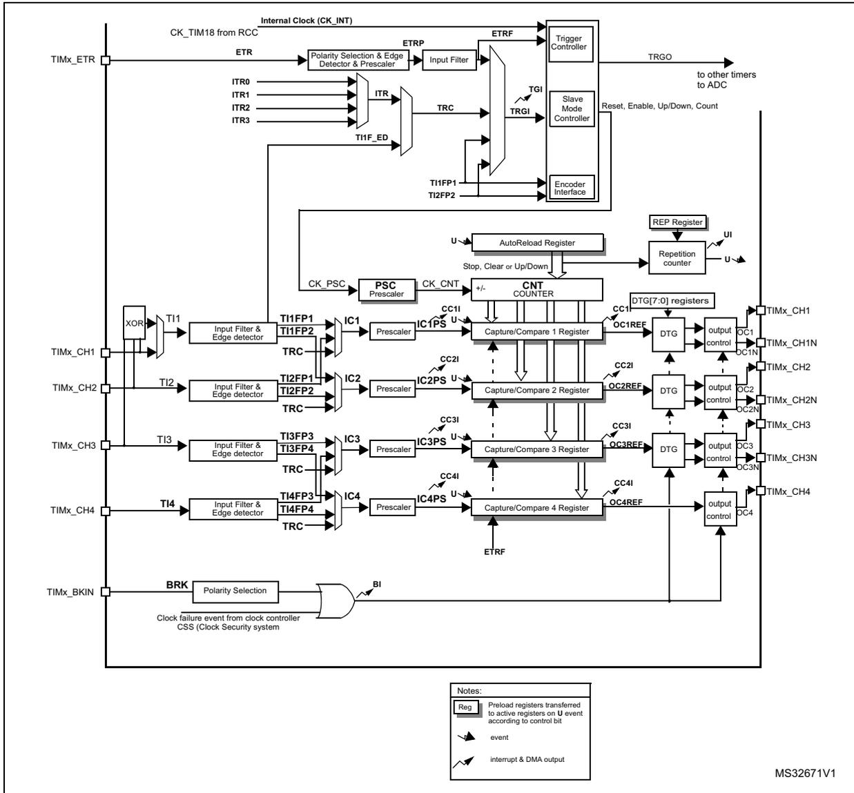
The diagram illustrates the internal architecture of the Advanced-control timer (TIM1). At the top, the Internal Clock (CK_INT) and CK_TIM18 from RCC are connected to the Trigger Controller . The TIMx_ETR input passes through a Polarity Selection & Edge Detector & Prescaler to produce ETRP , which is filtered by an Input Filter to generate ETRF . This ETRF signal is fed into the Trigger Controller . The Trigger Controller also receives ITR0 , ITR1 , ITR2 , and ITR3 inputs via an ITR block, and TI1F_ED from the Encoder Interface . It outputs TRGO to other timers and the ADC , and provides Reset, Enable, Up/Down, Count signals to the Slave Mode Controller . The Slave Mode Controller is connected to the Encoder Interface which takes TI1FP1 and TI2FP2 as inputs. The AutoReload Register and REP Register are connected to the REP counter , which outputs UI to the AutoReload Register . The AutoReload Register provides Stop, Clear or Up/Down signals to the CNT COUNTER . The CNT COUNTER is clocked by CK_PSC from the PSC Prescaler and outputs CK_CNT . The PSC Prescaler also receives CC1 from the Capture/Compare 1 Register . The CNT COUNTER is connected to four Capture/Compare Register blocks (1, 2, 3, and 4). Each register has associated prescalers ( IC1PS , IC2PS , IC3PS , IC4PS ) and DTG[7:0] registers. The Capture/Compare Register 1 outputs CC1 to the DTG[7:0] registers and OC1REF to the output control block. The output control block generates OC1 , OC1N , OC2 , OC2N , OC3 , OC3N , and OC4 outputs. The DTG[7:0] registers also provide OC1REF , OC2REF , OC3REF , and OC4REF signals. The TI1 , TI2 , TI3 , and TI4 inputs are processed by Input Filter & Edge detector blocks to produce IC1 , IC2 , IC3 , and IC4 signals. These signals are also filtered by Input Filter & Edge detector blocks to produce TRC signals. The TRC signals are fed into the Trigger Controller . The BRK input is processed by a Polarity Selection block to produce BI , which is also fed into the Trigger Controller . The Clock failure event from clock controller CSS (Clock Security system) is also fed into the Trigger Controller . A Notes box at the bottom right explains the symbols used: Reg for preload registers transferred to active registers on U event according to control bit, event for a signal transition, and interrupt & DMA output for a signal with an interrupt/DMA output symbol.
MS32671V1
12.3 TIM1 functional description
12.3.1 Time-base unit
The main block of the programmable advanced-control timer is a 16-bit counter with its related auto-reload register. The counter can count up, down or both up and down. The counter clock can be divided by a prescaler.
The counter, the auto-reload register and the prescaler register can be written or read by software. This is true even when the counter is running.
The time-base unit includes:
- • Counter register (TIMx_CNT)
- • Prescaler register (TIMx_PSC)
- • Auto-reload register (TIMx_ARR)
- • Repetition counter register (TIMx_RCR)
The auto-reload register is preloaded. Writing to or reading from the auto-reload register accesses the preload register. The content of the preload register are transferred into the shadow register permanently or at each update event (UEV), depending on the auto-reload preload enable bit (ARPE) in TIMx_CR1 register. The update event is sent when the counter reaches the overflow (or underflow when downcounting) and if the UDIS bit equals 0 in the TIMx_CR1 register. It can also be generated by software. The generation of the update event is described in detailed for each configuration.
The counter is clocked by the prescaler output CK_CNT, which is enabled only when the counter enable bit (CEN) in TIMx_CR1 register is set (refer also to the slave mode controller description to get more details on counter enabling).
Note that the counter starts counting 1 clock cycle after setting the CEN bit in the TIMx_CR1 register.
Prescaler description
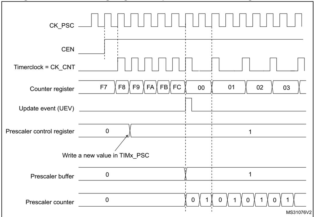
The prescaler can divide the counter clock frequency by any factor between 1 and 65536. It is based on a 16-bit counter controlled through a 16-bit register (in the TIMx_PSC register). It can be changed on the fly as this control register is buffered. The new prescaler ratio is taken into account at the next update event.
Figure 40 and Figure 41 give some examples of the counter behavior when the prescaler ratio is changed on the fly:
Figure 40. Counter timing diagram with prescaler division change from 1 to 2
This timing diagram illustrates the operation of an advanced-control timer (TIM1) when the prescaler division is changed from 1 to 2. The diagram includes the following signals and registers over time:
- CK_PSC : Prescaler clock signal, shown as a continuous square wave.
- CEN : Counter Enable signal, which goes high to start the counter.
- Timerclock = CK_CNT : The clock signal for the counter, which is derived from CK_PSC. Its frequency changes when the prescaler division changes.
- Counter register : Shows the counter values. It counts from F7 to FC, then rolls over to 00. After the prescaler change, it counts 00, 01, 02, 03 before rolling over.
- Update event (UEV) : A pulse generated when the counter rolls over from FC to 00.
- Prescaler control register : Initially set to 0 (division 1). A write operation occurs at the first UEV, changing the value to 1 (division 2).
- Prescaler buffer : A buffer that latches the new prescaler value (1) at the next UEV.
- Prescaler counter : A counter that divides the CK_PSC frequency. It counts 0, 1 (division 1) initially, then after the change, it counts 0, 1, 0, 1, 0, 1, 0, 1 (division 2).
Annotation: Write a new value in TIMx_PSC (pointing to the change in the Prescaler control register).
Reference: MS31076V2
Figure 41. Counter timing diagram with prescaler division change from 1 to 4
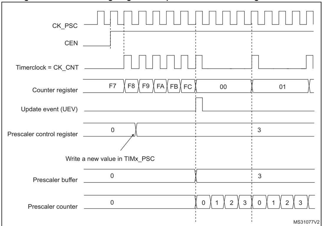
This timing diagram illustrates the operation of an advanced-control timer (TIM1) when the prescaler division is changed from 1 to 4. The diagram includes the following signals and registers over time:
- CK_PSC : Prescaler clock signal, shown as a continuous square wave.
- CEN : Counter Enable signal, which goes high to start the counter.
- Timerclock = CK_CNT : The clock signal for the counter, which is derived from CK_PSC. Its frequency changes when the prescaler division changes.
- Counter register : Shows the counter values. It counts from F7 to FC, then rolls over to 00. After the prescaler change, it counts 00, 01 before rolling over.
- Update event (UEV) : A pulse generated when the counter rolls over from FC to 00.
- Prescaler control register : Initially set to 0 (division 1). A write operation occurs at the first UEV, changing the value to 3 (division 4).
- Prescaler buffer : A buffer that latches the new prescaler value (3) at the next UEV.
- Prescaler counter : A counter that divides the CK_PSC frequency. It counts 0, 1 (division 1) initially, then after the change, it counts 0, 1, 2, 3, 0, 1, 2, 3 (division 4).
Annotation: Write a new value in TIMx_PSC (pointing to the change in the Prescaler control register).
Reference: MS31077V2
12.3.2 Counter modes
Upcounting mode
In upcounting mode, the counter counts from 0 to the auto-reload value (content of the TIMx_ARR register), then restarts from 0 and generates a counter overflow event.
If the repetition counter is used, the update event (UEV) is generated after upcounting is repeated for the number of times programmed in the repetition counter register (TIMx_RCR). Else the update event is generated at each counter overflow.
Setting the UG bit in the TIMx_EGR register (by software or by using the slave mode controller) also generates an update event.
The UEV event can be disabled by software by setting the UDIS bit in the TIMx_CR1 register. This is to avoid updating the shadow registers while writing new values in the preload registers. Then no update event occurs until the UDIS bit has been written to 0. However, the counter restarts from 0, as well as the counter of the prescaler (but the prescale rate does not change). In addition, if the URS bit (update request selection) in TIMx_CR1 register is set, setting the UG bit generates an update event UEV but without setting the UIF flag (thus no interrupt or DMA request is sent). This is to avoid generating both update and capture interrupts when clearing the counter on the capture event.
When an update event occurs, all the registers are updated and the update flag (UIF bit in TIMx_SR register) is set (depending on the URS bit):
- • The repetition counter is reloaded with the content of TIMx_RCR register,
- • The auto-reload shadow register is updated with the preload value (TIMx_ARR),
- • The buffer of the prescaler is reloaded with the preload value (content of the TIMx_PSC register).
The following figures show some examples of the counter behavior for different clock frequencies when TIMx_ARR=0x36.
Figure 42. Counter timing diagram, internal clock divided by 1
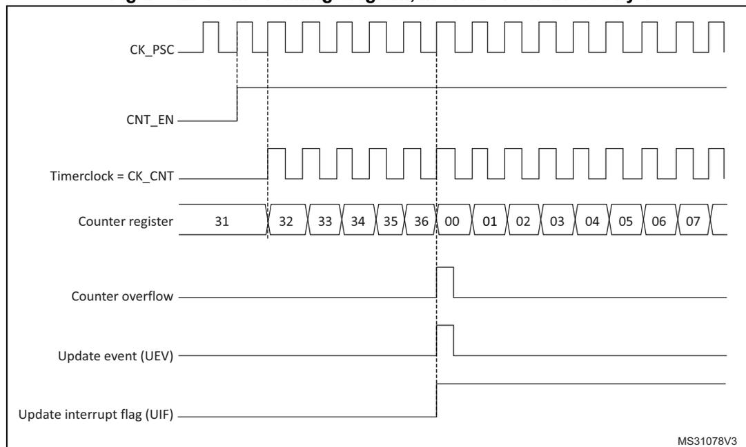
The timing diagram illustrates the counter's behavior in upcounting mode. The top signal, CK_PSC, is a periodic square wave. Below it, CNT_EN is a horizontal line that goes high to enable the counter. The third signal, Timerclock = CK_CNT, is a square wave that is active only when CNT_EN is high. The fourth signal, 'Counter register', shows a sequence of values: 31, 32, 33, 34, 35, 36, 00, 01, 02, 03, 04, 05, 06, 07. The values 32 through 36 are highlighted with a shaded background. The fifth signal, 'Counter overflow', is a pulse that goes high when the counter reaches 36 and returns low when it rolls over to 00. The sixth signal, 'Update event (UEV)', is a pulse that goes high at the same time as the counter overflow. The bottom signal, 'Update interrupt flag (UIF)', is a pulse that goes high at the same time as the counter overflow and returns low at the same time as the UEV pulse returns low. Vertical dashed lines indicate the timing relationships between the signals. The diagram is labeled MS31078V3 in the bottom right corner.
Figure 43. Counter timing diagram, internal clock divided by 2
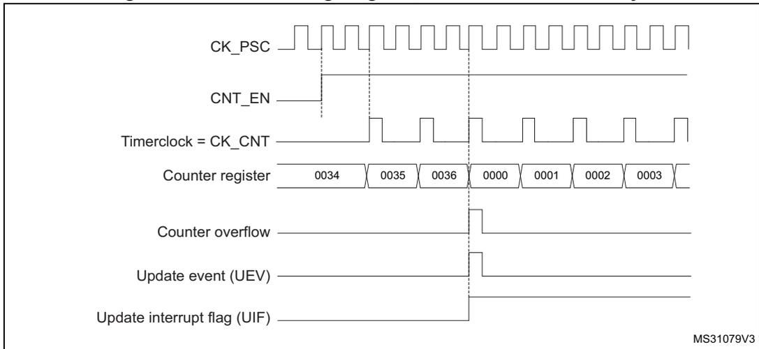
This timing diagram illustrates the operation of the counter when the internal clock is divided by 2. The top signal, CK_PSC, is a periodic square wave. Below it, CNT_EN is shown as a high-level signal. The Timerclock = CK_CNT signal is a square wave with a frequency half that of CK_PSC. The Counter register is shown with a sequence of values: 0034, 0035, 0036, 0000, 0001, 0002, and 0003. A Counter overflow pulse occurs when the counter transitions from 0036 to 0000. The Update event (UEV) and Update interrupt flag (UIF) are shown as pulses that coincide with the counter overflow. The diagram is labeled MS31079V3 in the bottom right corner.
Figure 44. Counter timing diagram, internal clock divided by 4
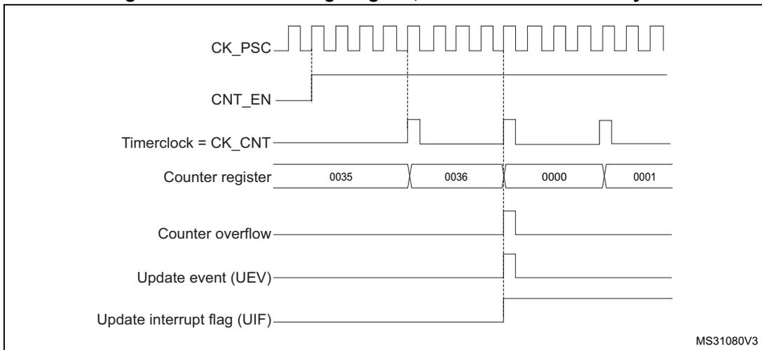
This timing diagram illustrates the operation of the counter when the internal clock is divided by 4. The top signal, CK_PSC, is a periodic square wave. Below it, CNT_EN is shown as a high-level signal. The Timerclock = CK_CNT signal is a square wave with a frequency one-quarter that of CK_PSC. The Counter register is shown with values 0035, 0036, 0000, and 0001. A Counter overflow pulse occurs when the counter transitions from 0036 to 0000. The Update event (UEV) and Update interrupt flag (UIF) are shown as pulses that coincide with the counter overflow. The diagram is labeled MS31080V3 in the bottom right corner.
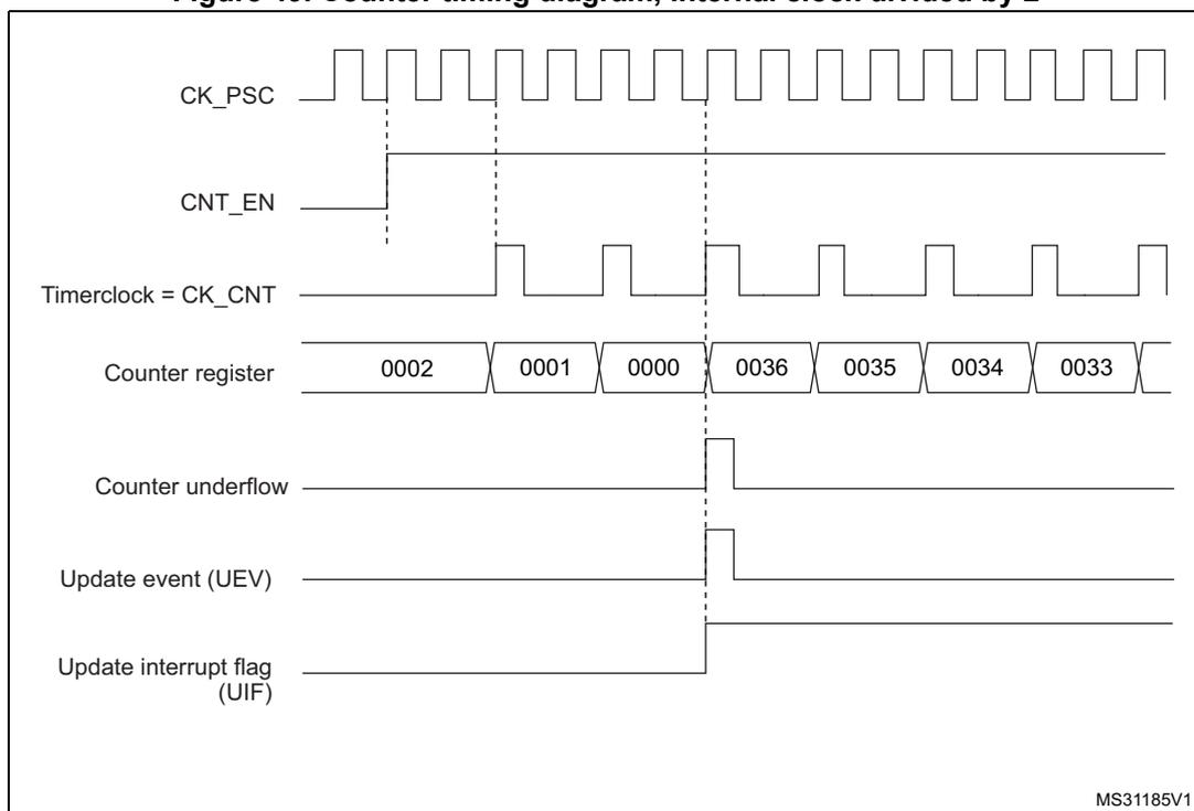
Figure 45. Counter timing diagram, internal clock divided by N
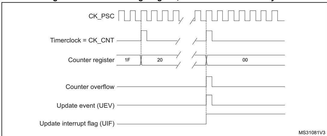
This timing diagram illustrates the operation of the counter when the internal clock is divided by an arbitrary factor N. The top signal, CK_PSC, is a periodic square wave. Below it, the Timerclock = CK_CNT signal is shown with a break in the waveform, indicating a lower frequency. The Counter register is shown with values 1F, 20, and 00. A Counter overflow pulse occurs when the counter transitions from 20 to 00. The Update event (UEV) and Update interrupt flag (UIF) are shown as pulses that coincide with the counter overflow. The diagram is labeled MS31081V3 in the bottom right corner.
Figure 46. Counter timing diagram, update event when ARPE=0 (TIMx_ARR not preloaded)
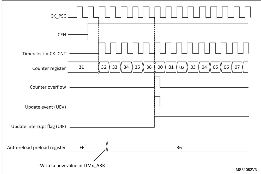
Timing diagram for Figure 46 (ARPE=0):
- CK_PSC: System clock signal.
- CEN: Counter Enable signal, active high.
- Timerclock = CK_CNT: Counter clock signal, derived from CK_PSC.
- Counter register: Shows values 31, 32, 33, 34, 35, 36, 00, 01, 02, 03, 04, 05, 06, 07. The counter increments on each rising edge of the timer clock.
- Counter overflow: Signal that goes high when the counter reaches its maximum value (36) and rolls over to 00.
- Update event (UEV): Signal that goes high when the counter overflows.
- Update interrupt flag (UIF): Signal that goes high when the counter overflows.
- Auto-reload preload register: Shows values FF and 36. An arrow points to the register with the text "Write a new value in TIMx_ARR".
MS31082V3
Figure 47. Counter timing diagram, update event when ARPE=1 (TIMx_ARR preloaded)
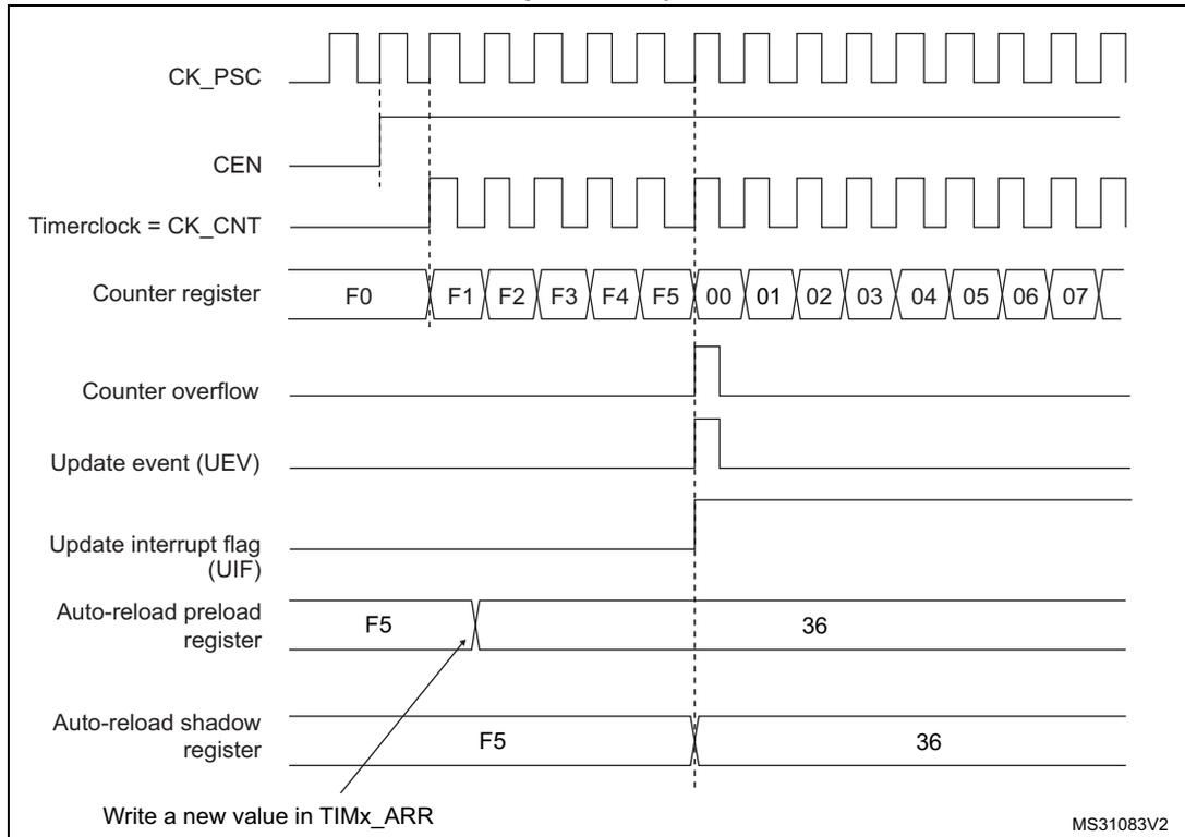
Timing diagram for Figure 47 (ARPE=1):
- CK_PSC: System clock signal.
- CEN: Counter Enable signal, active high.
- Timerclock = CK_CNT: Counter clock signal, derived from CK_PSC.
- Counter register: Shows values F0, F1, F2, F3, F4, F5, 00, 01, 02, 03, 04, 05, 06, 07. The counter increments on each rising edge of the timer clock.
- Counter overflow: Signal that goes high when the counter reaches its maximum value (F5) and rolls over to 00.
- Update event (UEV): Signal that goes high when the counter overflows.
- Update interrupt flag (UIF): Signal that goes high when the counter overflows.
- Auto-reload preload register: Shows values F5 and 36. An arrow points to the register with the text "Write a new value in TIMx_ARR".
- Auto-reload shadow register: Shows values F5 and 36. This register is updated from the preload register when the counter overflows.
MS31083V2
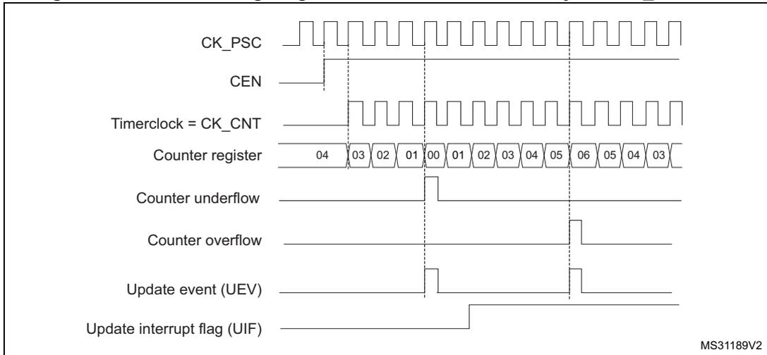
Downcounting mode
In downcounting mode, the counter counts from the auto-reload value (content of the TIMx_ARR register) down to 0, then restarts from the auto-reload value and generates a counter underflow event.
If the repetition counter is used, the update event (UEV) is generated after downcounting is repeated for the number of times programmed in the repetition counter register plus one (TIMx_RCR+1). Else the update event is generated at each counter underflow.
Setting the UG bit in the TIMx_EGR register (by software or by using the slave mode controller) also generates an update event.
The UEV update event can be disabled by software by setting the UDIS bit in TIMx_CR1 register. This is to avoid updating the shadow registers while writing new values in the preload registers. Then no update event occurs until UDIS bit has been written to 0. However, the counter restarts from the current auto-reload value, whereas the counter of the prescaler restarts from 0 (but the prescale rate doesn't change).
In addition, if the URS bit (update request selection) in TIMx_CR1 register is set, setting the UG bit generates an update event UEV but without setting the UIF flag (thus no interrupt or DMA request is sent). This is to avoid generating both update and capture interrupts when clearing the counter on the capture event.
When an update event occurs, all the registers are updated and the update flag (UIF bit in TIMx_SR register) is set (depending on the URS bit):
- • The repetition counter is reloaded with the content of TIMx_RCR register
- • The buffer of the prescaler is reloaded with the preload value (content of the TIMx_PSC register)
- • The auto-reload active register is updated with the preload value (content of the TIMx_ARR register). Note that the auto-reload is updated before the counter is reloaded, so that the next period is the expected one
The following figures show some examples of the counter behavior for different clock frequencies when TIMx_ARR=0x36.
Figure 48. Counter timing diagram, internal clock divided by 1
Timing diagram showing the relationship between the prescaler clock (CK_PSC), counter enable (CNT_EN), timer clock (Timerclock = CK_CNT), counter register values, counter underflow (cnt_udf), update event (UEV), and update interrupt flag (UIF) when the internal clock is divided by 1.
The diagram illustrates the following signals and events:
- CK_PSC : Prescaler clock signal, shown as a square wave.
- CNT_EN : Counter enable signal, which goes high to start counting.
- Timerclock = CK_CNT : Counter clock signal, which is the output of the prescaler.
- Counter register : Shows the sequence of counter values: 05, 04, 03, 02, 01, 00, 36, 35, 34, 33, 32, 31, 30, 2F. The transition from 00 to 36 indicates a counter underflow.
- Counter underflow (cnt_udf) : A pulse generated when the counter rolls over from 00 to 36.
- Update event (UEV) : A pulse generated when the counter rolls over.
- Update interrupt flag (UIF) : A pulse generated when the counter rolls over.
MS31184V1
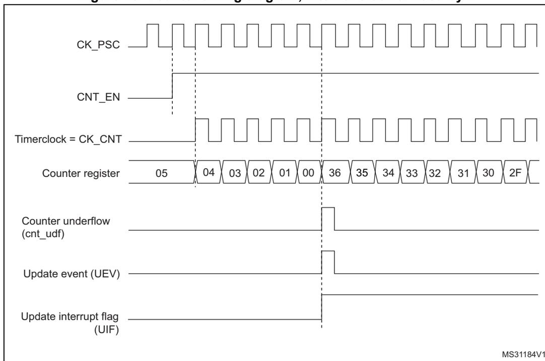
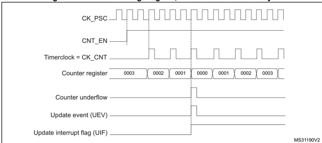
Figure 49. Counter timing diagram, internal clock divided by 2
Timing diagram showing the relationship between the prescaler clock (CK_PSC), counter enable (CNT_EN), timer clock (Timerclock = CK_CNT), counter register values, counter underflow (cnt_udf), update event (UEV), and update interrupt flag (UIF) when the internal clock is divided by 2.
The diagram illustrates the following signals and events:
- CK_PSC : Prescaler clock signal, shown as a square wave.
- CNT_EN : Counter enable signal, which goes high to start counting.
- Timerclock = CK_CNT : Counter clock signal, which is the output of the prescaler (divided by 2).
- Counter register : Shows the sequence of counter values: 0002, 0001, 0000, 0036, 0035, 0034, 0033. The transition from 0000 to 0036 indicates a counter underflow.
- Counter underflow : A pulse generated when the counter rolls over from 0000 to 0036.
- Update event (UEV) : A pulse generated when the counter rolls over.
- Update interrupt flag (UIF) : A pulse generated when the counter rolls over.
MS31185V1
Figure 50. Counter timing diagram, internal clock divided by 4
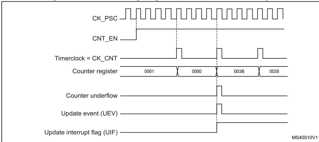
This timing diagram illustrates the operation of an advanced-control timer (TIM1) with its internal clock divided by 4. The diagram shows the relationship between the prescaler clock (CK_PSC), the counter enable signal (CNT_EN), the timer clock (Timerclock = CK_CNT), the counter register values, the counter underflow signal, the update event (UEV), and the update interrupt flag (UIF). The counter register values shown are 0001, 0000, 0036, and 0035. The counter underflow, UEV, and UIF signals are shown as pulses that occur when the counter register reaches 0000. The diagram is labeled MS40510V1.
Figure 51. Counter timing diagram, internal clock divided by N
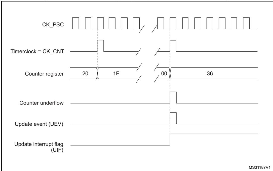
This timing diagram illustrates the operation of an advanced-control timer (TIM1) with its internal clock divided by N. The diagram shows the relationship between the prescaler clock (CK_PSC), the timer clock (Timerclock = CK_CNT), the counter register values, the counter underflow signal, the update event (UEV), and the update interrupt flag (UIF). The counter register values shown are 20, 1F, 00, and 36. The counter underflow, UEV, and UIF signals are shown as pulses that occur when the counter register reaches 00. The diagram is labeled MS31187V1.
Figure 52. Counter timing diagram, update event when repetition counter is not used
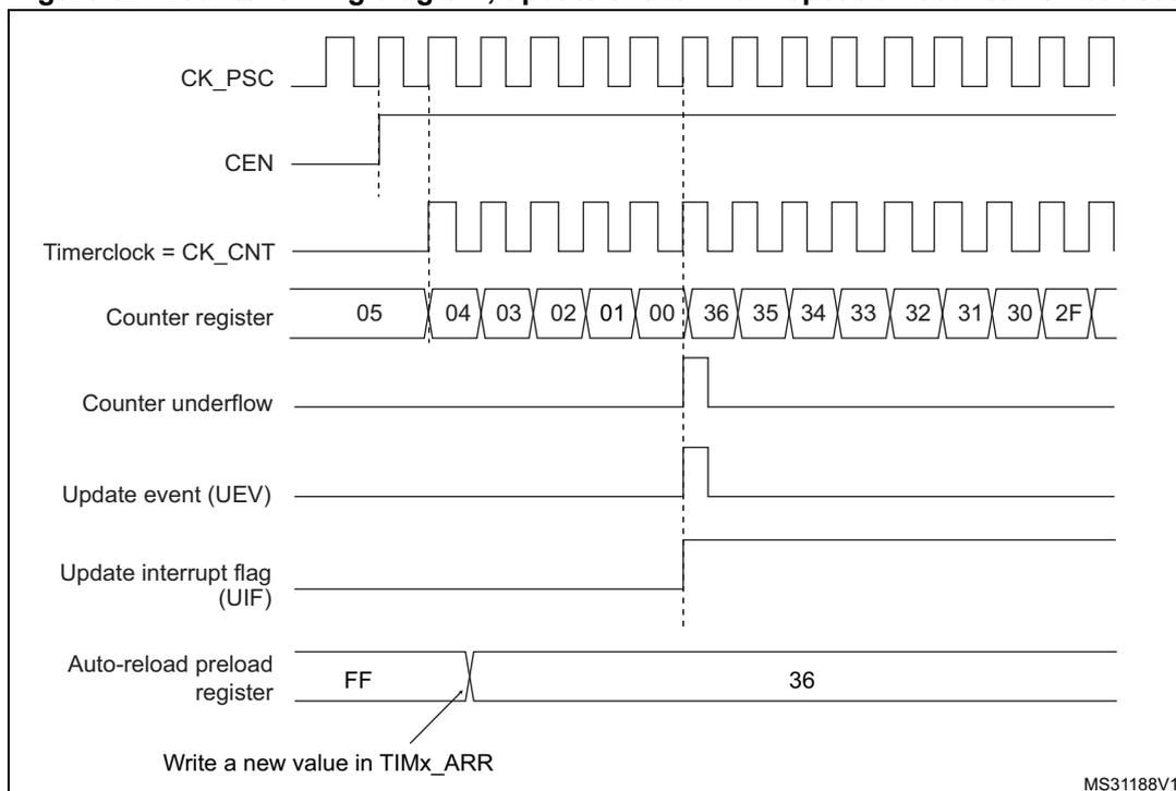
The timing diagram illustrates the operation of the counter. The CK_PSC signal is a periodic clock. The CEN signal is active-low, indicated by the bubble at its input. The Timerclock = CK_CNT is derived from CK_PSC when CEN is active. The Counter register shows values decreasing from 05 to 00, then jumping to 36 and continuing to decrease to 2F. The Counter underflow signal is active-low and pulses when the counter reaches 00. The Update event (UEV) is active-low and pulses when the counter reaches 00. The Update interrupt flag (UIF) is active-low and is set when the counter reaches 00. The Auto-reload preload register contains the value FF, which is then updated to 36. A note indicates that a new value can be written in the TIMx_ARR register.
MS31188V1
Center-aligned mode (up/down counting)
In center-aligned mode, the counter counts from 0 to the auto-reload value (content of the TIMx_ARR register) – 1, generates a counter overflow event, then counts from the auto-reload value down to 1 and generates a counter underflow event. Then it restarts counting from 0.
Center-aligned mode is active when the CMS bits in TIMx_CR1 register are not equal to '00'. The Output compare interrupt flag of channels configured in output is set when: the counter counts down (Center aligned mode 1, CMS = "01"), the counter counts up (Center aligned mode 2, CMS = "10") the counter counts up and down (Center aligned mode 3, CMS = "11").
In this mode, the DIR direction bit in the TIMx_CR1 register cannot be written. It is updated by hardware and gives the current direction of the counter.
The update event can be generated at each counter overflow and at each counter underflow or by setting the UG bit in the TIMx_EGR register (by software or by using the slave mode controller) also generates an update event. In this case, the counter restarts counting from 0, as well as the counter of the prescaler.
The UEV update event can be disabled by software by setting the UDIS bit in the TIMx_CR1 register. This is to avoid updating the shadow registers while writing new values in the preload registers. Then no update event occurs until UDIS bit has been written to 0. However, the counter continues counting up and down, based on the current auto-reload value.
In addition, if the URS bit (update request selection) in TIMx_CR1 register is set, setting the UG bit generates an UEV update event but without setting the UIF flag (thus no interrupt or DMA request is sent). This is to avoid generating both update and capture interrupts when clearing the counter on the capture event.
When an update event occurs, all the registers are updated and the update flag (UIF bit in TIMx_SR register) is set (depending on the URS bit):
- • The repetition counter is reloaded with the content of TIMx_RCR register
- • The buffer of the prescaler is reloaded with the preload value (content of the TIMx_PSC register)
- • The auto-reload active register is updated with the preload value (content of the TIMx_ARR register). Note that if the update source is a counter overflow, the auto-reload is updated before the counter is reloaded, so that the next period is the expected one (the counter is loaded with the new value).
The following figures show some examples of the counter behavior for different clock frequencies.
Figure 53. Counter timing diagram, internal clock divided by 1, TIMx_ARR=0x6
This timing diagram illustrates the behavior of the TIM1 counter when the internal clock is divided by 1 and the auto-reload register (TIMx_ARR) is set to 0x6. The diagram shows several signal levels over time:
- CK_PSC : A periodic square wave representing the prescaler output clock.
- CEN : Counter Enable signal, shown as a high-level pulse.
- Timerclock = CK_CNT : The clock signal for the counter, which is a higher-frequency square wave derived from CK_PSC.
- Counter register : Displays the counter's value over time: 04, 03, 02, 01, 00, 01, 02, 03, 04, 05, 06, 05, 04, 03. This indicates a center-aligned mode where the counter counts up from 00 to 06 and then back down to 00.
- Counter underflow : A pulse generated when the counter reaches 00.
- Counter overflow : A pulse generated when the counter reaches 06.
- Update event (UEV) : Pulses that occur at both the underflow and overflow events.
- Update interrupt flag (UIF) : A signal that goes high upon an update event and remains high until cleared.
1. Here, center-aligned mode 1 is used (for more details refer to Section 12.4: TIM1 registers ).
Figure 54. Counter timing diagram, internal clock divided by 2
This timing diagram illustrates the behavior of the TIM1 counter when the internal clock is divided by 2. The diagram shows several signal levels over time:
- CK_PSC : A periodic square wave representing the prescaler output clock.
- CNT_EN : Counter Enable signal, shown as a high-level pulse.
- Timerclock = CK_CNT : The clock signal for the counter, which has a lower frequency than in Figure 53 due to the division by 2.
- Counter register : Displays the counter's value over time: 0003, 0002, 0001, 0000, 0001, 0002, 0003. This indicates a center-aligned mode with an auto-reload value of 0003.
- Counter underflow : A pulse generated when the counter reaches 0000.
- Update event (UEV) : A pulse that occurs at the underflow event.
- Update interrupt flag (UIF) : A signal that goes high upon an update event and remains high until cleared.
Figure 55. Counter timing diagram, internal clock divided by 4, TIMx_ARR=0x36
This timing diagram illustrates the operation of an advanced-control timer (TIM1) in center-aligned mode. The top signal, CK_PSC, is a periodic square wave representing the prescaler clock. Below it, CNT_EN is a horizontal line indicating the counter is enabled. The Timerclock = CK_CNT signal is a square wave derived from CK_PSC, with a frequency divided by 4. The Counter register shows a sequence of values: 0034, 0035, 0036, and 0035. A 'Counter overflow' pulse occurs when the counter reaches 0036 and rolls over to 0035. Simultaneously, an 'Update event (UEV)' and an 'Update interrupt flag (UIF)' are generated. The diagram is labeled MS31191V2 in the bottom right corner.
- 1. Center-aligned mode 2 or 3 is used with an UIF on overflow.
Figure 56. Counter timing diagram, internal clock divided by N
This timing diagram shows the counter's behavior when the internal clock is divided by N. The CK_PSC signal is shown at the top. The Timerclock = CK_CNT signal is a square wave with a frequency divided by N. The Counter register displays values in hexadecimal: 20, 1F, 01, and 00. A 'Counter underflow' occurs as the counter rolls over from 00 back to 20. At this transition, an 'Update event (UEV)' and an 'Update interrupt flag (UIF)' are asserted. The diagram is labeled MS31192V2 in the bottom right corner.
Figure 57. Counter timing diagram, update event with ARPE=1 (counter underflow)
The diagram illustrates the timing of a counter underflow. The CK_PSC signal is a periodic clock. CEN is high, enabling the counter. The Timer clock (CK_CNT) is derived from CK_PSC. The Counter register starts at 06 and counts down: 05, 04, 03, 02, 01, 00. At 00, the Counter overflow signal goes high, followed by the Update event (UEV) and the Update interrupt flag (UIF). The Auto-reload preload register is initially FD and is updated to 36. The Auto-reload active register is initially FD and is updated to 36 at the underflow event. A note indicates 'Write a new value in TIMx_ARR' pointing to the preload register update. The diagram is labeled MS31193V3.
Figure 58. Counter timing diagram, Update event with ARPE=1 (counter overflow)
The diagram illustrates the timing of a counter overflow. The CK_PSC signal is a periodic clock. CEN is high, enabling the counter. The Timer clock (CK_CNT) is derived from CK_PSC. The Counter register starts at F7 and counts up: F8, F9, FA, FB, FC. At FC, the Counter overflow signal goes high, followed by the Update event (UEV) and the Update interrupt flag (UIF). The register then jumps to 36 and counts down: 35, 34, 33, 32, 31, 30, 2F. The Auto-reload preload register is initially FD and is updated to 36. The Auto-reload active register is initially FD and is updated to 36 at the overflow event. A note indicates 'Write a new value in TIMx_ARR' pointing to the preload register update. The diagram is labeled MS31194V2.
12.3.3 Repetition counter
Section 12.3.1 describes how the update event (UEV) is generated with respect to the counter overflows/underflows. It is actually generated only when the repetition counter has reached zero. This can be useful when generating PWM signals.
This means that data are transferred from the preload registers to the shadow registers (TIMx_ARR auto-reload register, TIMx_PSC prescaler register, but also TIMx_CCRx capture/compare registers in compare mode) every N+1 counter overflows or underflows, where N is the value in the TIMx_RCR repetition counter register.
The repetition counter is decremented:
- • At each counter overflow in upcounting mode,
- • At each counter underflow in downcounting mode,
- • At each counter overflow and at each counter underflow in center-aligned mode.
- Although this limits the maximum number of repetition to 128 PWM cycles, it makes it possible to update the duty cycle twice per PWM period. When refreshing compare registers only once per PWM period in center-aligned mode, maximum resolution is \( 2 \times T_{ck} \) , due to the symmetry of the pattern.
The repetition counter is an auto-reload type; the repetition rate is maintained as defined by the TIMx_RCR register value (refer to Figure 59). When the update event is generated by software (by setting the UG bit in TIMx_EGR register) or by hardware through the slave mode controller, it occurs immediately whatever the value of the repetition counter is and the repetition counter is reloaded with the content of the TIMx_RCR register.
In center-aligned mode, for odd values of RCR, the update event occurs either on the overflow or on the underflow depending on when the RCR register was written and when the counter was started. If the RCR was written before starting the counter, the UEV occurs on the overflow. If the RCR was written after starting the counter, the UEV occurs on the underflow. For example for RCR = 3, the UEV is generated on each 4th overflow or underflow event depending on when RCR was written.
Figure 59. Update rate examples depending on mode and TIMx_RCR register settings
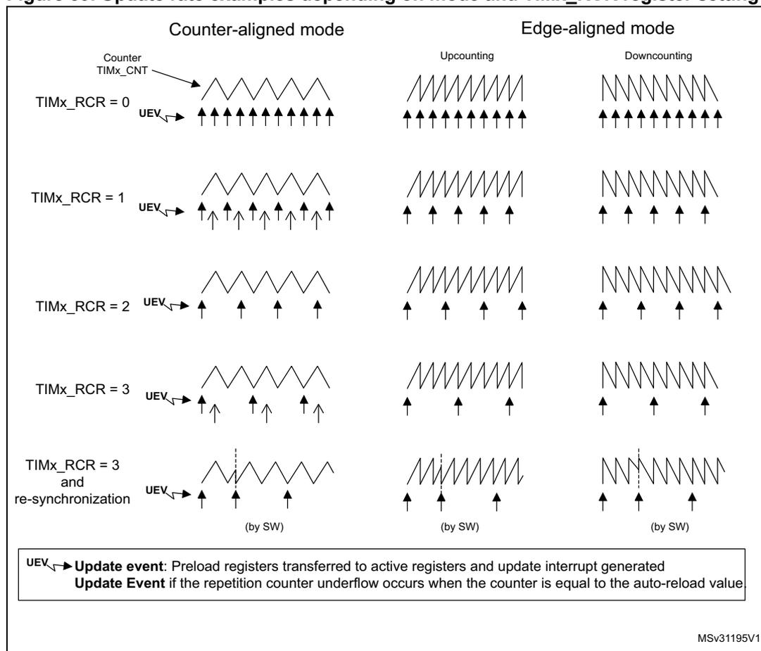
The figure illustrates the update rate for different timer modes and repetition counter (RCR) settings. It is divided into three main columns: Counter-aligned mode, Edge-aligned mode (Upcounting), and Edge-aligned mode (Downcounting). Rows represent different TIMx_RCR values: 0, 1, 2, 3, and 3 with re-synchronization. Waveforms show the counter (TIMx_CNT) and the repetition counter (TIMx_RCR) over time. Update events (UEV) are marked with arrows. In the 'TIMx_RCR = 3 and re-synchronization' row, the first UEV is followed by a 'by SW' label, indicating a software-generated update event.
Legend:
UEV →
Update event:
Preload registers transferred to active registers and update interrupt generated
Update Event
if the repetition counter underflow occurs when the counter is equal to the auto-reload value.
MSv31195V1
12.3.4 Clock selection
The counter clock can be provided by the following clock sources:
- • Internal clock (CK_INT)
- • External clock mode1: external input pin
- • External clock mode2: external trigger input ETR
- • Internal trigger inputs (ITRx): using one timer as prescaler for another timer, for example, the user can configure Timer 1 to act as a prescaler for Timer 2. Refer to Using one timer as prescaler for another timer for more details.
Internal clock source (CK_INT)
If the slave mode controller is disabled (SMS=000), then the CEN, DIR (in the TIMx_CR1 register) and UG bits (in the TIMx_EGR register) are actual control bits and can be changed only by software (except UG which remains cleared automatically). As soon as the CEN bit is written to 1, the prescaler is clocked by the internal clock CK_INT.
Figure 60 shows the behavior of the control circuit and the upcounter in normal mode, without prescaler.
Figure 60. Control circuit in normal mode, internal clock divided by 1
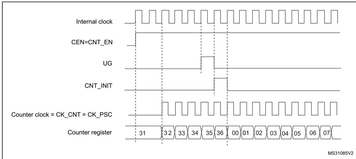
The timing diagram illustrates the control circuit and counter behavior. The 'Internal clock' is a continuous square wave. The 'CEN=CNT_EN' signal is initially low and transitions to high at the first vertical dashed line. The 'UG' signal is initially low and transitions to high at the second vertical dashed line. The 'CNT_INIT' signal is initially high and transitions to low at the third vertical dashed line. The 'Counter clock = CK_CNT = CK_PSC' signal is initially low and transitions to a square wave at the first vertical dashed line. The 'Counter register' shows a sequence of values: 31, 32, 33, 34, 35, 36, 00, 01, 02, 03, 04, 05, 06, 07. The values 31 through 36 are shown in individual boxes, followed by 00 through 07 in individual boxes. The counter increments by 1 at each rising edge of the counter clock, starting from 31 and rolling over from 36 to 00.
External clock source mode 1
This mode is selected when SMS=111 in the TIMx_SMCR register. The counter can count at each rising or falling edge on a selected input.
Figure 61. TI2 external clock connection example
![Block diagram of TI2 external clock connection example. The diagram shows the signal flow from the TI2 input through a filter (controlled by ICF[3:0] in TIMx_CCMR1) and an edge detector (controlled by CC2P in TIMx_CCER). The edge detector outputs TI2F_Rising and TI2F_Falling signals. These are multiplexed (0 for Rising, 1 for Falling) and then connected to a trigger input source selection block. This block includes options: ITRx (0xx), TI1_ED (100), TI1FP1 (101), TI2FP2 (110), and ETRF (111). The selected signal is then connected to a clock mode selection block. This block includes options: TRGI (TI2F falling or TI1F falling), ETRF (external clock), and CK_INT (internal clock). The clock mode selection is controlled by TS[2:0] in TIMx_SMCR. The output of the clock mode selection is CK_PSC. The clock mode selection block also includes options for Encoder mode, External clock mode 1, External clock mode 2, and Internal clock mode, controlled by ECE and SMS[2:0] in TIMx_SMCR.](/RM0383-STM32F411xC-E/ee9ec9df0528b0bc5018e4d2d640207f_img.jpg)
MS31196V1
For example, to configure the upcounter to count in response to a rising edge on the TI2 input, use the following procedure:
- 1. Configure channel 2 to detect rising edges on the TI2 input by writing CC2S = '01' in the TIMx_CCMR1 register.
- 2. Configure the input filter duration by writing the IC2F[3:0] bits in the TIMx_CCMR1 register (if no filter is needed, keep IC2F=0000).
- 3. Select rising edge polarity by writing CC2P=0 and CC2NP=0 in the TIMx_CCER register.
- 4. Configure the timer in external clock mode 1 by writing SMS=111 in the TIMx_SMCR register.
- 5. Select TI2 as the trigger input source by writing TS=110 in the TIMx_SMCR register.
- 6. Enable the counter by writing CEN=1 in the TIMx_CR1 register.
Note: The capture prescaler is not used for triggering, so the user does not need to configure it.
When a rising edge occurs on TI2, the counter counts once and the TIF flag is set.
The delay between the rising edge on TI2 and the actual clock of the counter is due to the resynchronization circuit on TI2 input.
Figure 62. Control circuit in external clock mode 1
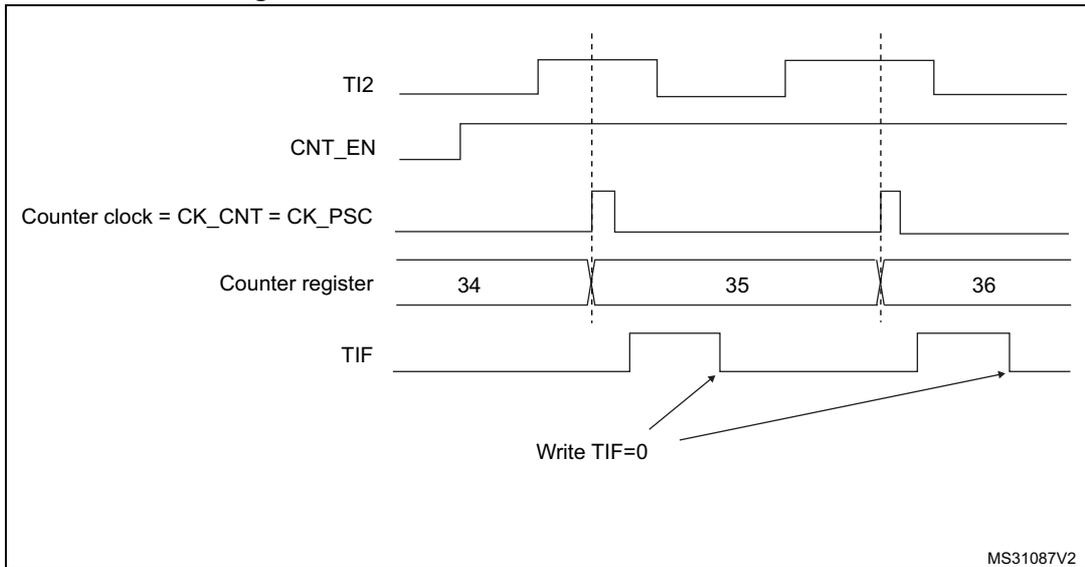
The diagram shows the relationship between several signals in external clock mode 1. The TI2 signal is a periodic square wave. The CNT_EN signal is a horizontal line indicating the counter is enabled. The Counter clock (CK_CNT = CK_PSC) is a square wave that toggles on the rising edges of TI2. The Counter register shows values 34, 35, and 36, with increments occurring at the rising edges of the counter clock. The TIF signal is a pulse that goes high when the counter overflows (from 35 to 36) and returns low when TIF=0 is written. A note 'Write TIF=0' has arrows pointing to the falling edges of the TIF signal.
External clock source mode 2
This mode is selected by writing ECE=1 in the TIMx_SMCR register.
The counter can count at each rising or falling edge on the external trigger input ETR.
Figure 63 gives an overview of the external trigger input block.
Figure 63. External trigger input block
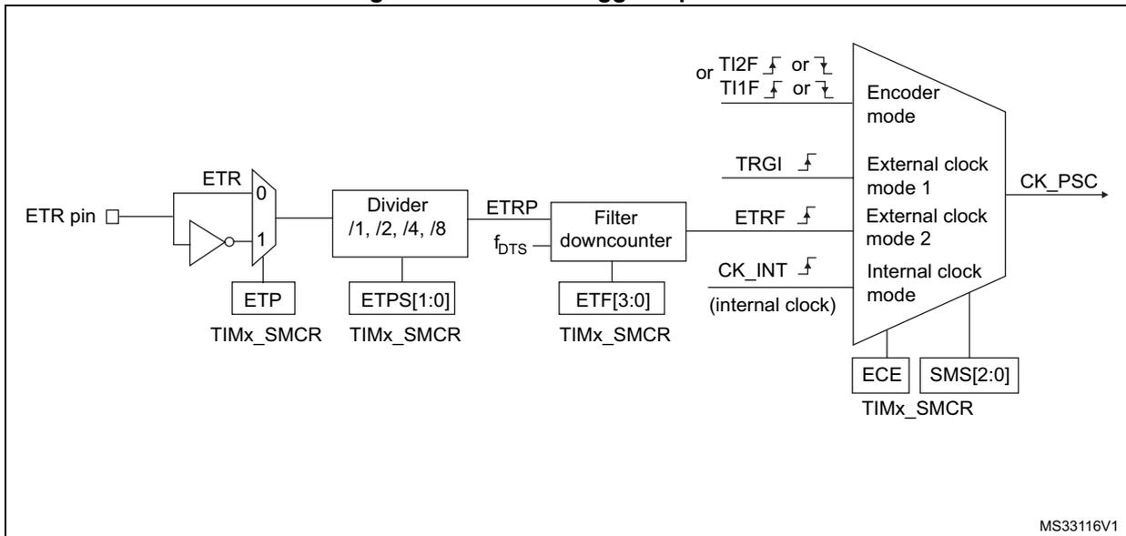
The diagram illustrates the external trigger input block. The ETR pin is connected to a multiplexer (ETR) with two inputs: 0 (direct) and 1 (inverted). The output of the multiplexer goes to a 'Divider /1, /2, /4, /8'. This divider is controlled by the ETPS[1:0] bits in the TIMx_SMCR register. The output of the divider is ETRP. ETRP goes to a 'Filter downcounter' which is controlled by the ETF[3:0] bits in the TIMx_SMCR register. The output of the filter is ETRF. ETRF is one of the inputs to a clock selection multiplexer. Other inputs to this multiplexer are TRGI, CK_INT (internal clock), or TI2F or TI1F. The multiplexer is controlled by the ECE and SMS[2:0] bits in the TIMx_SMCR register. The output of the multiplexer is CK_PSC, which is the counter clock.
For example, to configure the upcounter to count each 2 rising edges on ETR, use the following procedure:
- 1. As no filter is needed in this example, write ETF[3:0]=0000 in the TIMx_SMCR register.
- 2. Set the prescaler by writing ETPS[1:0]=01 in the TIMx_SMCR register
- 3. Select rising edge detection on the ETR pin by writing ETP=0 in the TIMx_SMCR register
- 4. Enable external clock mode 2 by writing ECE=1 in the TIMx_SMCR register.
- 5. Enable the counter by writing CEN=1 in the TIMx_CR1 register.
The counter counts once each 2 ETR rising edges.
The delay between the rising edge on ETR and the actual clock of the counter is due to the resynchronization circuit on the ETRP signal.
Figure 64. Control circuit in external clock mode 2
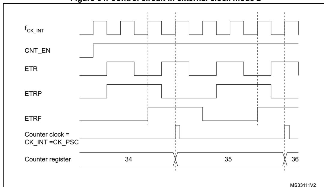
The timing diagram illustrates the relationship between several signals in external clock mode 2. The signals shown are:
- f CK_INT : Internal clock signal, a periodic square wave.
- CNT_EN : Counter enable signal, which goes high to enable counting.
- ETR : External trigger signal, showing multiple rising edges.
- ETRP : Resynchronized trigger signal, which follows ETR with some delay and jitter.
- ETRF : Filtered trigger signal, derived from ETR.
- Counter clock = CK INT = CK PSC : The clock used for the counter, which is the internal clock.
- Counter register : Shows the count values 34, 35, and 36. The count increments by 1 for every two rising edges of the ETR signal.
12.3.5 Capture/compare channels
Each Capture/Compare channel is built around a capture/compare register (including a shadow register), a input stage for capture (with digital filter, multiplexing and prescaler) and an output stage (with comparator and output control).
Figure 65 to Figure 68 give an overview of one Capture/Compare channel.
The input stage samples the corresponding TIx input to generate a filtered signal TIxF. Then, an edge detector with polarity selection generates a signal (TIxFPx) which can be used as trigger input by the slave mode controller or as the capture command. It is prescaled before the capture register (ICxPS).
Figure 65. Capture/compare channel (example: channel 1 input stage)
![Figure 65: Capture/compare channel (example: channel 1 input stage) block diagram. The diagram shows the input stage for channel 1. TI1 is filtered by a 'Filter downcounter' (controlled by ICF[3:0] from TIMx_CCMR1) to produce TI1F. This is then processed by an 'Edge detector' to produce TI1F_Rising and TI1F_Falling signals. These signals are multiplexed with signals from channel 2 (TI2F_Rising, TI2F_Falling) to produce TI1FP1 and TI2FP1. TI1FP1 is ANDed with TI1F_ED to produce an interrupt signal. TI2FP1 is used as the IC1 input, which is then divided by a 'Divider /1, /2, /4, /8' (controlled by ICPS[1:0] from TIMx_CCMR1) to produce IC1PS. The TRC signal from the slave mode controller is also used in the multiplexing stage. Control signals include CC1P/CC1NP, TIMx_CCER, and CC1S[1:0].](/RM0383-STM32F411xC-E/b2f6158e74f297659bf41c5939b2c1e0_img.jpg)
The output stage generates an intermediate waveform that is then used for reference: OCxRef (active high). The polarity acts at the end of the chain.
Figure 66. Capture/compare channel 1 main circuit
![Figure 66: Capture/compare channel 1 main circuit block diagram. This diagram shows the main circuit for channel 1. It includes an 'APB Bus' connected to an 'MCU-peripheral interface'. The interface controls a 'Capture/compare preload register' and a 'Capture/compare shadow register'. The preload register is loaded from the APB Bus (CCR1H and CCR1L) and its contents are transferred to the shadow register via 'capture_transfer' or 'compare_transfer' signals. The shadow register's output is compared with the 'Counter' value in a 'Comparator' to generate 'CNT>CCR1' and 'CNT=CCR1' signals. The 'Counter' is controlled by 'Capture' and 'Output mode' signals. The 'Capture' signal is generated by an AND gate of 'Input mode' (determined by CC1S[1] and CC1S[0]) and 'IC1PS' and 'CC1E'. The 'Output mode' is determined by 'write_in_progress' and 'UEV' (from time base unit). The 'UEV' signal is also used to generate 'OC1PE'. The 'OC1PE' signal is ANDed with 'CC1S[1]' and 'CC1S[0]' to produce the final output. Control signals include Read CCR1H, Read CCR1L, CC1G, and TIMx_EGR.](/RM0383-STM32F411xC-E/5a3009de5b031b84b643edc33b5b6f78_img.jpg)
Figure 67. Output stage of capture/compare channel (channel 1 to 3)
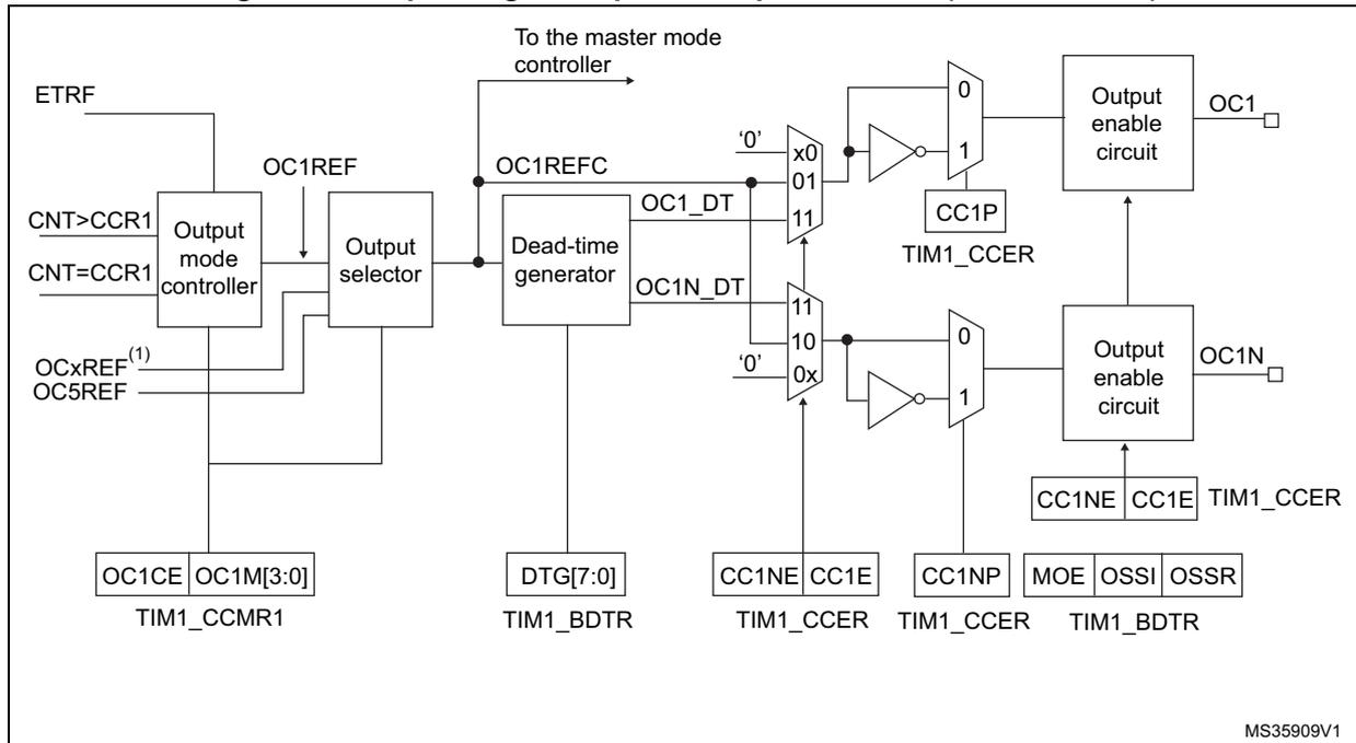
The diagram illustrates the output stage for channels 1 to 3. It starts with the ETRF input and CNT registers (CNT>CCR1 and CNT=CCR1) feeding into an 'Output mode controller'. This controller also receives OCxREF/OC5REF signals and control bits from TIM1_CCMR1 (OC1CE, OC1M[3:0]). The output of the controller goes to an 'Output selector', which produces OC1REF. OC1REF is connected to the 'master mode controller' and the 'Dead-time generator'. The Dead-time generator also receives DTG[7:0] from TIM1_BDTR and produces OC1_DT and OC1N_DT signals. These signals pass through multiplexers (selecting between '0', '1', or the dead-time signal) and inverters. The multiplexers are controlled by CC1P, CC1NE, and CC1E from TIM1_CCER. The outputs of the inverters go to 'Output enable circuit' blocks, which also receive inputs from CC1NP, MOE, OSSI, and OSSR from TIM1_BDTR. The final outputs are OC1 and OC1N. A reference label MS35909V1 is present in the bottom right.
Figure 68. Output stage of capture/compare channel (channel 4)
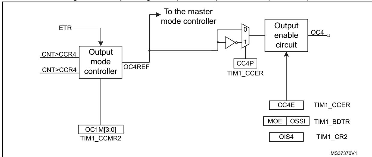
The diagram illustrates the output stage for channel 4. It starts with the ETR input and CNT registers (CNT>CCR4) feeding into an 'Output mode controller'. This controller also receives control bits from TIM1_CCMR2 (OC1M[3:0]). The output of the controller goes to an 'Output selector', which produces OC4REF. OC4REF is connected to the 'master mode controller' and an inverter. The inverter's output goes to an 'Output enable circuit' for OC4. This circuit also receives inputs from CC4P from TIM1_CCER, CC4E from TIM1_CCER, MOE and OSSI from TIM1_BDTR, and OIS4 from TIM1_CR2. The final output is OC4. A reference label MS37370V1 is present in the bottom right.
The capture/compare block is made of one preload register and one shadow register. Write and read always access the preload register.
In capture mode, captures are actually done in the shadow register, which is copied into the preload register.
In compare mode, the content of the preload register is copied into the shadow register which is compared to the counter.
12.3.6 Input capture mode
In Input capture mode, the Capture/Compare registers (TIMx_CCRx) are used to latch the value of the counter after a transition detected by the corresponding ICx signal. When a capture occurs, the corresponding CCxIF flag (TIMx_SR register) is set and an interrupt or a DMA request can be sent if they are enabled. If a capture occurs while the CCxIF flag was already high, then the over-capture flag CCxOF (TIMx_SR register) is set. CCxIF can be cleared by software by writing it to '0' or by reading the captured data stored in the TIMx_CCRx register. CCxOF is cleared when written to '0'.
The following example shows how to capture the counter value in TIMx_CCR1 when TI1 input rises. To do this, use the following procedure:
- • Select the active input: TIMx_CCR1 must be linked to the TI1 input, so write the CC1S bits to 01 in the TIMx_CCMR1 register. As soon as CC1S becomes different from 00, the channel is configured in input and the TIMx_CCR1 register becomes read-only.
- • Program the needed input filter duration with respect to the signal connected to the timer (by programming ICxF bits in the TIMx_CCMRx register if the input is a TIx input). Let's imagine that, when toggling, the input signal is not stable during at most five internal clock cycles. We must program a filter duration longer than these five clock cycles. We can validate a transition on TI1 when 8 consecutive samples with the new level have been detected (sampled at \( f_{DTS} \) frequency). Then write IC1F bits to 0011 in the TIMx_CCMR1 register.
- • Select the edge of the active transition on the TI1 channel by writing CC1P and CC1NP bits to 0 in the TIMx_CCER register (rising edge in this case).
- • Program the input prescaler. In our example, we wish the capture to be performed at each valid transition, so the prescaler is disabled (write IC1PS bits to '00' in the TIMx_CCMR1 register).
- • Enable capture from the counter into the capture register by setting the CC1E bit in the TIMx_CCER register.
- • If needed, enable the related interrupt request by setting the CC1IE bit in the TIMx_DIER register, and/or the DMA request by setting the CC1DE bit in the TIMx_DIER register.
When an input capture occurs:
- • The TIMx_CCR1 register gets the value of the counter on the active transition.
- • CC1IF flag is set (interrupt flag). CC1OF is also set if at least two consecutive captures occurred whereas the flag was not cleared.
- • An interrupt is generated depending on the CC1IE bit.
- • A DMA request is generated depending on the CC1DE bit.
In order to handle the overcapture, it is recommended to read the data before the overcapture flag. This is to avoid missing an overcapture which could happen after reading the flag and before reading the data.
Note: IC interrupt and/or DMA requests can be generated by software by setting the corresponding CCxG bit in the TIMx_EGR register.
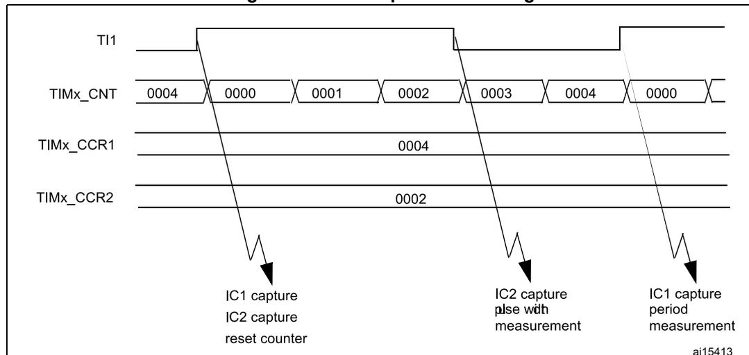
12.3.7 PWM input mode
This mode is a particular case of input capture mode. The procedure is the same except:
- • Two ICx signals are mapped on the same TIx input.
- • These 2 ICx signals are active on edges with opposite polarity.
- • One of the two TIxFP signals is selected as trigger input and the slave mode controller is configured in reset mode.
For example, user can measure the period (in TIMx_CCR1 register) and the duty cycle (in TIMx_CCR2 register) of the PWM applied on TI1 using the following procedure (depending on CK_INT frequency and prescaler value):
- • Select the active input for TIMx_CCR1: write the CC1S bits to 01 in the TIMx_CCMR1 register (TI1 selected).
- • Select the active polarity for TI1FP1 (used both for capture in TIMx_CCR1 and counter clear): write the CC1P and CC1NP bits to '0' (active on rising edge).
- • Select the active input for TIMx_CCR2: write the CC2S bits to 10 in the TIMx_CCMR1 register (TI1 selected).
- • Select the active polarity for TI1FP2 (used for capture in TIMx_CCR2): write the CC2P bit to '1' and the CC2NP bit to '0' (active on falling edge).
- • Select the valid trigger input: write the TS bits to 101 in the TIMx_SMCR register (TI1FP1 selected).
- • Configure the slave mode controller in reset mode: write the SMS bits to 100 in the TIMx_SMCR register.
- • Enable the captures: write the CC1E and CC2E bits to '1' in the TIMx_CCER register.
Figure 69. PWM input mode timing
12.3.8 Forced output mode
In output mode (CCxS bits = 00 in the TIMx_CCMRx register), each output compare signal (OCxREF and then OCx/OCxN) can be forced to active or inactive level directly by software, independently of any comparison between the output compare register and the counter.
To force an output compare signal (OCxREF/OCx) to its active level, the user just needs to write 101 in the OCxM bits in the corresponding TIMx_CCMRx register. Thus OCxREF is
forced high (OCxREF is always active high) and OCx get opposite value to CCxP polarity bit.
For example: CCxP=0 (OCx active high) => OCx is forced to high level.
The OCxREF signal can be forced low by writing the OCxM bits to 100 in the TIMx_CCMRx register.
Anyway, the comparison between the TIMx_CCRx shadow register and the counter is still performed and allows the flag to be set. Interrupt and DMA requests can be sent accordingly. This is described in the output compare mode section below.
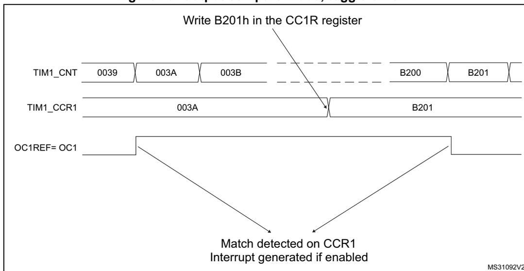
12.3.9 Output compare mode
This function is used to control an output waveform or indicating when a period of time has elapsed.
When a match is found between the capture/compare register and the counter, the output compare function:
- • Assigns the corresponding output pin to a programmable value defined by the output compare mode (OCxM bits in the TIMx_CCMRx register) and the output polarity (CCxP bit in the TIMx_CCER register). The output pin can keep its level (OCxM=000), be set active (OCxM=001), be set inactive (OCxM=010) or can toggle (OCxM=011) on match.
- • Sets a flag in the interrupt status register (CCxIF bit in the TIMx_SR register).
- • Generates an interrupt if the corresponding interrupt mask is set (CCxIE bit in the TIMx_DIER register).
- • Sends a DMA request if the corresponding enable bit is set (CCxDE bit in the TIMx_DIER register, CCDS bit in the TIMx_CR2 register for the DMA request selection).
The TIMx_CCRx registers can be programmed with or without preload registers using the OCxPE bit in the TIMx_CCMRx register.
In output compare mode, the update event UEV has no effect on OCxREF and OCx output. The timing resolution is one count of the counter. Output compare mode can also be used to output a single pulse (in One Pulse mode).
Procedure:
- 1. Select the counter clock (internal, external, prescaler).
- 2. Write the desired data in the TIMx_ARR and TIMx_CCRx registers.
- 3. Set the CCxIE bit if an interrupt request is to be generated.
- 4. Select the output mode. For example:
- – Write OCxM = 011 to toggle OCx output pin when CNT matches CCRx
- – Write OCxPE = 0 to disable preload register
- – Write CCxP = 0 to select active high polarity
- – Write CCxE = 1 to enable the output
- 5. Enable the counter by setting the CEN bit in the TIMx_CR1 register.
The TIMx_CCRx register can be updated at any time by software to control the output waveform, provided that the preload register is not enabled (OCxPE='0', else TIMx_CCRx shadow register is updated only at the next update event UEV). An example is given in Figure 70 .
Figure 70. Output compare mode, toggle on OC1
12.3.10 PWM mode
Pulse Width Modulation mode allows generating a signal with a frequency determined by the value of the TIMx_ARR register and a duty cycle determined by the value of the TIMx_CCRx register.
The PWM mode can be selected independently on each channel (one PWM per OCx output) by writing '110' (PWM mode 1) or '111' (PWM mode 2) in the OCxM bits in the TIMx_CCMRx register. The corresponding preload register must be enabled by setting the OCxPE bit in the TIMx_CCMRx register, and eventually the auto-reload preload register (in upcounting or center-aligned modes) by setting the ARPE bit in the TIMx_CR1 register.
As the preload registers are transferred to the shadow registers only when an update event occurs, before starting the counter, the user must initialize all the registers by setting the UG bit in the TIMx_EGR register.
OCx polarity is software programmable using the CCxP bit in the TIMx_CCER register. It can be programmed as active high or active low. OCx output is enabled by a combination of the CCxE, CCxNE, MOE, OSSI and OSSR bits (TIMx_CCER and TIMx_BDTR registers). Refer to the TIMx_CCER register description for more details.
In PWM mode (1 or 2), TIMx_CNT and TIMx_CCRx are always compared to determine whether \( TIMx\_CCRx \leq TIMx\_CNT \) or \( TIMx\_CNT \leq TIMx\_CCRx \) (depending on the direction of the counter).
The timer is able to generate PWM in edge-aligned mode or center-aligned mode depending on the CMS bits in the TIMx_CR1 register.
PWM edge-aligned mode
- • Upcounting configuration
Upcounting is active when the DIR bit in the TIMx_CR1 register is low. Refer to Upcounting mode .
In the following example, we consider PWM mode 1. The reference PWM signal OCxREF is high as long as \( TIMx\_CNT < TIMx\_CCRx \) else it becomes low. If the
compare value in TIMx_CCRx is greater than the auto-reload value (in TIMx_ARR) then OCxREF is held at '1'. If the compare value is 0 then OCxRef is held at '0'.
Figure 71 shows some edge-aligned PWM waveforms in an example where TIMx_ARR=8.
Figure 71. Edge-aligned PWM waveforms (ARR=8)
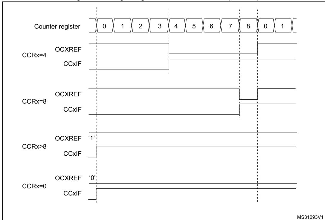
The figure illustrates the relationship between the counter register values and the resulting PWM signals for different compare register (CCR) settings. The counter register is shown at the top, cycling from 0 to 8 and then back to 0. Below it, four sets of waveforms are shown for different CCRx values: CCRx=4, CCRx=8, CCRx>8, and CCRx=0. Each set includes the OCxREF signal and the CCxIF flag. For CCRx=4, the OCxREF signal is high from counter value 0 to 4 and low from 4 to 8. For CCRx=8, the OCxREF signal is high from 0 to 8 and low from 8 to 0. For CCRx>8, the OCxREF signal is held high throughout the cycle. For CCRx=0, the OCxREF signal is held low throughout the cycle. The CCxIF flag is shown as a pulse when the counter value matches the CCRx value.
MS31093V1
- • Downcounting configuration
Downcounting is active when DIR bit in TIMx_CR1 register is high. Refer to Downcounting mode
In PWM mode 1, the reference signal OCxRef is low as long as \( TIMx\_CNT > TIMx\_CCRx \) else it becomes high. If the compare value in TIMx_CCRx is greater than the auto-reload value in TIMx_ARR, then OCxREF is held at '1'. 0% PWM is not possible in this mode.
PWM center-aligned mode
Center-aligned mode is active when the CMS bits in TIMx_CR1 register are different from '00' (all the remaining configurations having the same effect on the OCxRef/OCx signals). The compare flag is set when the counter counts up, when it counts down or both when it counts up and down depending on the CMS bits configuration. The direction bit (DIR) in the
TIMx_CR1 register is updated by hardware and must not be changed by software. Refer to Center-aligned mode (up/down counting) .
Figure 72 shows some center-aligned PWM waveforms in an example where:
- • TIMx_ARR=8,
- • PWM mode is the PWM mode 1,
- • The flag is set when the counter counts down corresponding to the center-aligned mode 1 selected for CMS=01 in TIMx_CR1 register.
Figure 72. Center-aligned PWM waveforms (ARR=8)
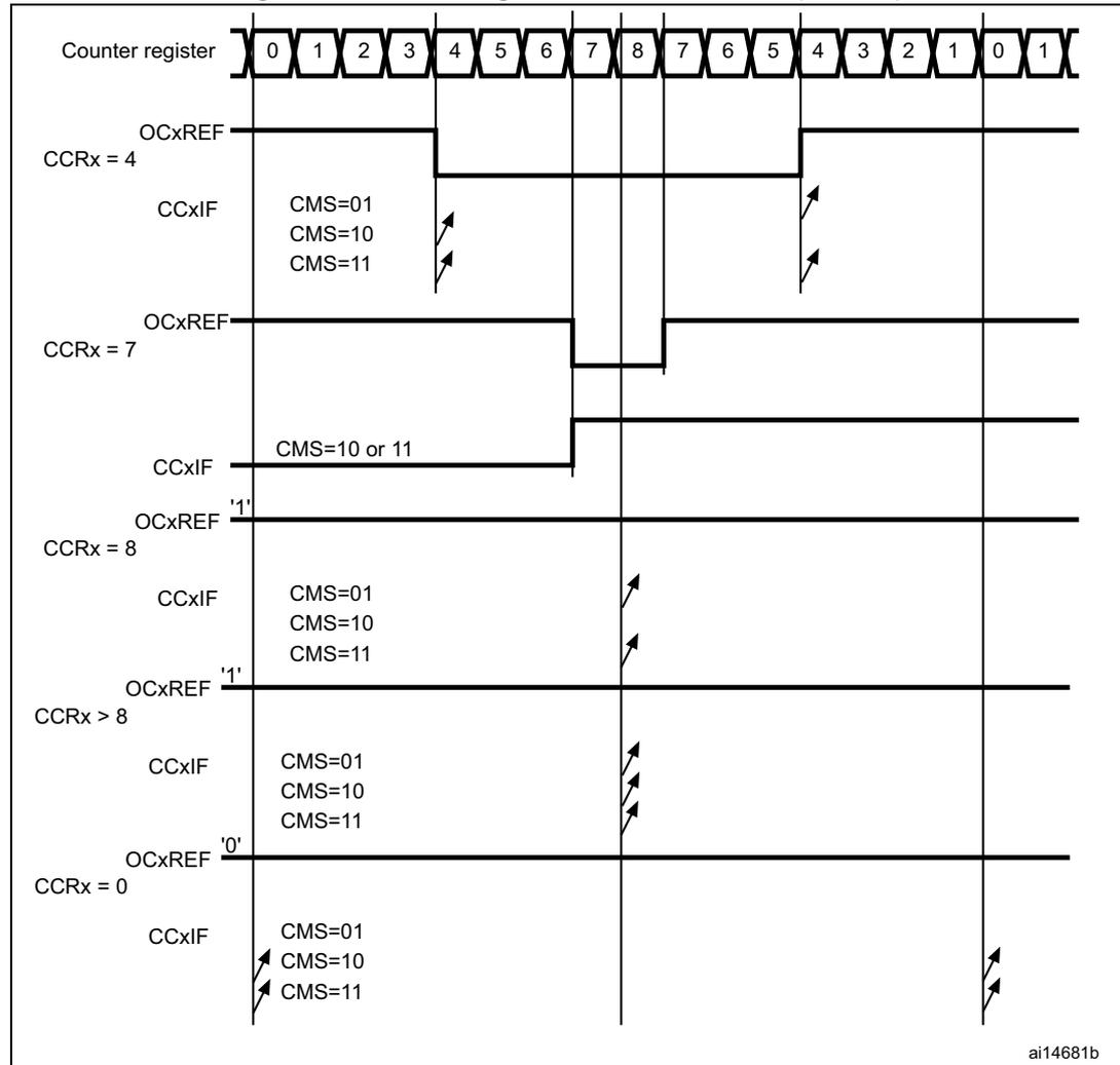
The figure illustrates the timing of center-aligned PWM waveforms for an Advanced-control timer (TIM1) with ARR=8. The counter register sequence is shown at the top, cycling from 0 to 8 and back down to 0, then starting up again. Below this, the OCxREF signal and CCxIF flag are shown for different CCRx values:
- CCRx = 4: The OCxREF signal is high from counter value 4 down to 0 and back up to 4. The CCxIF flag is set on the falling edge of OCxREF (when the counter counts down from 4 to 3) for CMS=01, CMS=10, and CMS=11.
- CCRx = 7: The OCxREF signal is high from counter value 7 down to 0 and back up to 7. The CCxIF flag is set on the falling edge of OCxREF (when the counter counts down from 7 to 6) for CMS=10 or 11.
- CCRx = 8: The OCxREF signal is high from counter value 8 down to 0 and back up to 8. The CCxIF flag is set on the falling edge of OCxREF (when the counter counts down from 8 to 7) for CMS=01, CMS=10, and CMS=11.
- CCRx > 8: The OCxREF signal is high from counter value 8 down to 0 and back up to 8. The CCxIF flag is set on the falling edge of OCxREF (when the counter counts down from 8 to 7) for CMS=01, CMS=10, and CMS=11.
- CCRx = 0: The OCxREF signal is high from counter value 0 down to 8 and back down to 0. The CCxIF flag is set on the falling edge of OCxREF (when the counter counts down from 1 to 0) for CMS=01, CMS=10, and CMS=11.
The diagram also shows the initial state of the OCxREF signal for each CCRx value: '1' for CCRx = 8, CCRx > 8, and CCRx = 0; and '0' for CCRx = 4 and CCRx = 7.
Hints on using center-aligned mode:
- • When starting in center-aligned mode, the current up-down configuration is used. It means that the counter counts up or down depending on the value written in the DIR bit
in the TIMx_CR1 register. Moreover, the DIR and CMS bits must not be changed at the same time by the software.
- • Writing to the counter while running in center-aligned mode is not recommended as it can lead to unexpected results. In particular:
- – The direction is not updated if the user writes a value in the counter greater than the auto-reload value (TIMx_CNT > TIMx_ARR). For example, if the counter was counting up, it continues to count up.
- – The direction is updated if the user writes 0 or write the TIMx_ARR value in the counter but no Update Event UEV is generated.
- • The safest way to use center-aligned mode is to generate an update by software (setting the UG bit in the TIMx_EGR register) just before starting the counter and not to write the counter while it is running.
12.3.11 Complementary outputs and dead-time insertion
The advanced-control timers (TIM1) can output two complementary signals and manage the switching-off and the switching-on instants of the outputs.
This time is generally known as dead-time and it has to be adjusted depending on the devices connected to the outputs and their characteristics (intrinsic delays of level-shifters, delays due to power switches...)
User can select the polarity of the outputs (main output OCx or complementary OCxN) independently for each output. This is done by writing to the CCxP and CCxNP bits in the TIMx_CCER register.
The complementary signals OCx and OCxN are activated by a combination of several control bits: the CCxE and CCxNE bits in the TIMx_CCER register and the MOE, OISx, OISxN, OSSI and OSSR bits in the TIMx_BDTR and TIMx_CR2 registers. Refer to Table 50 for more details. In particular, the dead-time is activated when switching to the IDLE state (MOE falling down to 0).
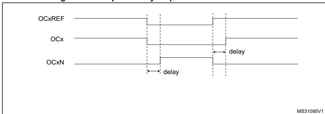
Dead-time insertion is enabled by setting both CCxE and CCxNE bits, and the MOE bit if the break circuit is present. DTG[7:0] bits of the TIMx_BDTR register are used to control the dead-time generation for all channels. From a reference waveform OCxREF, it generates 2 outputs OCx and OCxN. If OCx and OCxN are active high:
- • The OCx output signal is the same as the reference signal except for the rising edge, which is delayed relative to the reference rising edge.
- • The OCxN output signal is the opposite of the reference signal except for the rising edge, which is delayed relative to the reference falling edge.
If the delay is greater than the width of the active output (OCx or OCxN) then the corresponding pulse is not generated.
The following figures show the relationships between the output signals of the dead-time generator and the reference signal OCxREF. (we suppose CCxP=0, CCxNP=0, MOE=1, CCxE=1 and CCxNE=1 in these examples)
Figure 73. Complementary output with dead-time insertion
Timing diagram showing complementary output with dead-time insertion. The diagram displays three waveforms: OCxREF, OCx, and OCxN. OCxREF is a reference signal. OCx and OCxN are complementary outputs. Dead-time is indicated by 'delay' labels between the transitions of OCx and OCxN. The diagram is labeled MS31095V1.
Figure 74. Dead-time waveforms with delay greater than the negative pulse
Timing diagram showing dead-time waveforms with delay greater than the negative pulse. The diagram displays three waveforms: OCxREF, OCx, and OCxN. OCxREF is a reference signal. OCx and OCxN are complementary outputs. Dead-time is indicated by a 'delay' label between the transitions of OCx and OCxN. The diagram is labeled MS31096V1.
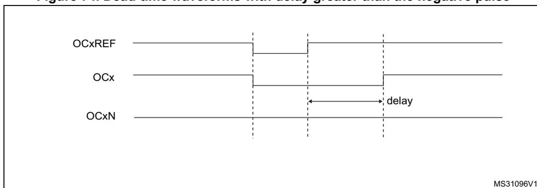
Figure 75. Dead-time waveforms with delay greater than the positive pulse
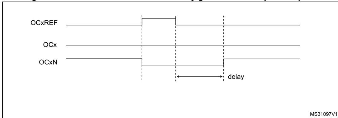
Timing diagram showing dead-time waveforms with delay greater than the positive pulse. The diagram displays three waveforms: OCxREF, OCx, and OCxN. OCxREF is a reference signal. OCx and OCxN are complementary outputs. Dead-time is indicated by a 'delay' label between the transitions of OCx and OCxN. The diagram is labeled MS31097V1.
The dead-time delay is the same for each of the channels and is programmable with the DTG bits in the TIMx_BDTR register. Refer to Section 12.4.18 for delay calculation.
Re-directing OCxREF to OCx or OCxN
In output mode (forced, output compare or PWM), OCxREF can be re-directed to the OCx output or to OCxN output by configuring the CCxE and CCxNE bits in the TIMx_CCER register.
This allows the user to send a specific waveform (such as PWM or static active level) on one output while the complementary remains at its inactive level. Other possibilities are to have both outputs at inactive level or both outputs active and complementary with
dead-time.
Note: When only OCxN is enabled (CCxE=0, CCxNE=1), it is not complemented and becomes active as soon as OCxREF is high. For example, if CCxNP=0 then OCxN=OCxRef. On the other hand, when both OCx and OCxN are enabled (CCxE=CCxNE=1) OCx becomes active when OCxREF is high whereas OCxN is complemented and becomes active when OCxREF is low.
12.3.12 Using the break function
When using the break function, the output enable signals and inactive levels are modified according to additional control bits (MOE, OSSI and OSSR bits in the TIMx_BDTR register, OISx and OISxN bits in the TIMx_CR2 register). In any case, the OCx and OCxN outputs cannot be set both to active level at a given time. Refer to Table 50 for more details.
The break source can be either the break input pin or a clock failure event, generated by the Clock Security System (CSS), from the Reset Clock Controller. For further information on the Clock Security System, refer to Section 6.2.7: Clock security system (CSS) .
When exiting from reset, the break circuit is disabled and the MOE bit is low. User can enable the break function by setting the BKE bit in the TIMx_BDTR register. The break input polarity can be selected by configuring the BKP bit in the same register. BKE and BKP can be modified at the same time. When the BKE and BKP bits are written, a delay of 1 APB clock cycle is applied before the writing is effective. Consequently, it is necessary to wait 1 APB clock period to correctly read back the bit after the write operation.
Because MOE falling edge can be asynchronous, a resynchronization circuit has been inserted between the actual signal (acting on the outputs) and the synchronous control bit (accessed in the TIMx_BDTR register). It results in some delays between the asynchronous and the synchronous signals. In particular, if MOE is written to 1 whereas it was low, a delay (dummy instruction) must be inserted before reading it correctly. This is because the user writes an asynchronous signal, but reads a synchronous signal.
When a break occurs (selected level on the break input):
- • The MOE bit is cleared asynchronously, putting the outputs in inactive state, idle state or in reset state (selected by the OSSI bit). This feature functions even if the MCU oscillator is off.
- • Each output channel is driven with the level programmed in the OISx bit in the TIMx_CR2 register as soon as MOE=0. If OSSI=0 then the timer releases the enable output else the enable output remains high.
- • When complementary outputs are used:
- – The outputs are first put in reset state inactive state (depending on the polarity). This is done asynchronously so that it works even if no clock is provided to the timer.
- – If the timer clock is still present, then the dead-time generator is reactivated in order to drive the outputs with the level programmed in the OISx and OISxN bits after a dead-time. Even in this case, OCx and OCxN cannot be driven to their active level together. Note that because of the resynchronization on MOE, the dead-time duration is a bit longer than usual (around 2 ck_tim clock cycles).
- – If OSSI=0 then the timer releases the enable outputs else the enable outputs remain or become high as soon as one of the CCxE or CCxNE bits is high.
- • The break status flag (BIF bit in the TIMx_SR register) is set. An interrupt can be generated if the BIE bit in the TIMx_DIER register is set. A DMA request can be sent if the BDE bit in the TIMx_DIER register is set.
- • If the AOE bit in the TIMx_BDTR register is set, the MOE bit is automatically set again at the next update event UEV. This can be used to perform a regulation, for instance. Else, MOE remains low until it is written to '1' again. In this case, it can be used for security and the break input can be connected to an alarm from power drivers, thermal sensors or any security components.
Note: The break inputs is acting on level. Thus, the MOE cannot be set while the break input is active (neither automatically nor by software). In the meantime, the status flag BIF cannot be cleared.
The break can be generated by the BRK input which has a programmable polarity and an enable bit BKE in the TIMx_BDTR register.
There are two solutions to generate a break:
- • By using the BRK input which has a programmable polarity and an enable bit BKE in the TIMx_BDTR register
- • By software through the BG bit of the TIMx_EGR register.
In addition to the break input and the output management, a write protection has been implemented inside the break circuit to safeguard the application. It allows freezing the configuration of several parameters (dead-time duration, OCx/OCxN polarities and state when disabled, OCxM configurations, break enable and polarity). The user can choose from three levels of protection selected by the LOCK bits in the TIMx_BDTR register. Refer to Section 12.4.18 . The LOCK bits can be written only once after an MCU reset.
Figure 76 shows an example of behavior of the outputs in response to a break.
Figure 76. Output behavior in response to a break
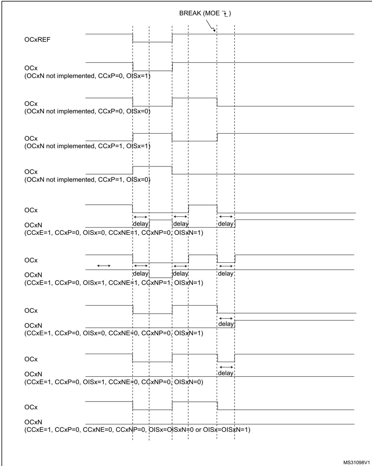
The timing diagram illustrates the behavior of various output pins in response to a break signal (BREAK (MOE ↓)). The diagram shows the state of the outputs before and after the break signal is asserted. The break signal is shown as a downward arrow at the top of the diagram.
The outputs shown are:
- OCxREF: Output reference signal.
- OCx (OCxN not implemented, CCxP=0, OISx=1): Output compare signal, active high.
- OCx (OCxN not implemented, CCxP=0, OISx=0): Output compare signal, active low.
- OCx (OCxN not implemented, CCxP=1, OISx=1): Output compare signal, active high.
- OCx (OCxN not implemented, CCxP=1, OISx=0): Output compare signal, active low.
- OCxN (CCxE=1, CCxP=0, OISx=0, CCxNE=1, CCxNP=0, OISxN=1): Inverted output compare signal, active low, with a delay indicated by a double-headed arrow.
- OCxN (CCxE=1, CCxP=0, OISx=1, CCxNE=1, CCxNP=1, OISxN=1): Inverted output compare signal, active high, with a delay indicated by a double-headed arrow.
- OCxN (CCxE=1, CCxP=0, OISx=0, CCxNE=0, CCxNP=0, OISxN=1): Inverted output compare signal, active low, with a delay indicated by a double-headed arrow.
- OCxN (CCxE=1, CCxP=0, OISx=1, CCxNE=0, CCxNP=0, OISxN=0): Inverted output compare signal, active high, with a delay indicated by a double-headed arrow.
- OCxN (CCxE=1, CCxP=0, CCxNE=0, CCxNP=0, OISx=0, OISxN=0 or OISx=OISxN=1): Inverted output compare signal, inactive.
The diagram shows that the break signal (BREAK (MOE ↓)) forces the OCxREF output to a low state. The other outputs (OCx and OCxN) are forced to a state determined by their configuration (active high or active low) when the break is asserted. The delay indicated by the double-headed arrows represents the time between the break signal assertion and the output state change.
MS31098V1
12.3.13 Clearing the OCxREF signal on an external event
The OCxREF signal for a given channel can be driven Low by applying a High level to the ETRF input (OCxCE enable bit of the corresponding TIMx_CCMRx register set to ‘1’). The OCxREF signal remains Low until the next update event, UEV, occurs.
This function can only be used in output compare and PWM modes, and does not work in forced mode.
For example, the ETR signal can be connected to the output of a comparator to be used for current handling. In this case, the ETR must be configured as follow:
- 1. The External Trigger Prescaler should be kept off: bits ETPS[1:0] of the TIMx_SMCR register set to ‘00’.
- 2. The external clock mode 2 must be disabled: bit ECE of the TIMx_SMCR register set to ‘0’.
- 3. The External Trigger Polarity (ETP) and the External Trigger Filter (ETF) can be configured according to the user needs.
Figure 77 shows the behavior of the OCxREF signal when the ETRF Input becomes High, for both values of the enable bit OCxCE. In this example, the timer TIMx is programmed in PWM mode.
Figure 77. Clearing TIMx OCxREF
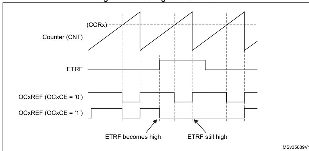
The timing diagram illustrates the interaction between the timer counter and external trigger.
-
Counter (CNT)
: A sawtooth waveform representing the timer value, with a dashed horizontal line indicating the
(CCRx)
threshold.
-
ETRF
: An external trigger signal that goes high for a duration spanning across two counter cycles.
-
OCxREF (OCxCE = '0')
: Shows the standard PWM output where the signal is high when CNT < CCRx and low when CNT > CCRx, unaffected by ETRF.
-
OCxREF (OCxCE = '1')
: Shows the modified behavior. When ETRF becomes high, the OCxREF signal is immediately forced low, even if CNT is still below CCRx. It remains low until the next counter overflow (update event), at which point it resumes its normal state unless ETRF is still high. The diagram points out 'ETRF becomes high' causing the signal to drop, and 'ETRF still high' showing it stays low through the next cycle until the next overflow.
Note: In case of a PWM with a 100% duty cycle (if CCRx>ARR), then OCxREF is enabled again at the next counter overflow.
12.3.14 6-step PWM generation
When complementary outputs are used on a channel, preload bits are available on the OCxM, CCxE and CCxNE bits. The preload bits are transferred to the shadow bits at the COM commutation event. The user can thus program in advance the configuration for the next step and change the configuration of all the channels at the same time. COM can be generated by software by setting the COM bit in the TIMx_EGR register or by hardware (on TRGI rising edge).
A flag is set when the COM event occurs (COMIF bit in the TIMx_SR register), which can generate an interrupt (if the COMIE bit is set in the TIMx_DIER register) or a DMA request (if the COMDE bit is set in the TIMx_DIER register).
Figure 78 describes the behavior of the OCx and OCxN outputs when a COM event occurs, in 3 different examples of programmed configurations.
Figure 78. 6-step generation, COM example (OSSR=1)
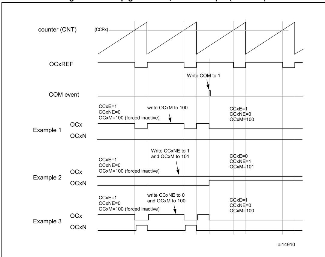
The timing diagram shows the relationship between the counter (CNT), the OCxREF signal, a COM event, and three examples of OCx and OCxN output behaviors.
- counter (CNT) (CCRx): A sawtooth waveform representing the counter value.
- OCxREF: A periodic signal that toggles based on the counter value.
- COM event: A pulse indicating a software-generated COM event (Write COM to 1).
- Example 1:
- Initial state: CCxE=1, CCxNE=0, OCxM=100 (forced inactive).
- Action: write OCxM to 100 (at a COM event).
- Final state: CCxE=1, CCxNE=0, OCxM=100.
- Example 2:
- Initial state: CCxE=1, CCxNE=0, OCxM=100 (forced inactive).
- Action: Write CCxNE to 1 and OCxM to 101 (at a COM event).
- Final state: CCxE=0, CCxNE=1, OCxM=101.
- Example 3:
- Initial state: CCxE=1, CCxNE=0, OCxM=100 (forced inactive).
- Action: write CCxNE to 0 and OCxM to 100 (at a COM event).
- Final state: CCxE=1, CCxNE=0, OCxM=100.
ai14910
12.3.15 One-pulse mode
One-pulse mode (OPM) is a particular case of the previous modes. It allows the counter to be started in response to a stimulus and to generate a pulse with a programmable length after a programmable delay.
Starting the counter can be controlled through the slave mode controller. Generating the waveform can be done in output compare mode or PWM mode. Select One-pulse mode by setting the OPM bit in the TIMx_CR1 register. This makes the counter stop automatically at the next update event UEV.
A pulse can be correctly generated only if the compare value is different from the counter initial value. Before starting (when the timer is waiting for the trigger), the configuration must be:
- • In upcounting: \( CNT < CCRx \leq ARR \) (in particular, \( 0 < CCRx \) )
- • In downcounting: \( CNT > CCRx \)
Figure 79. Example of one pulse mode
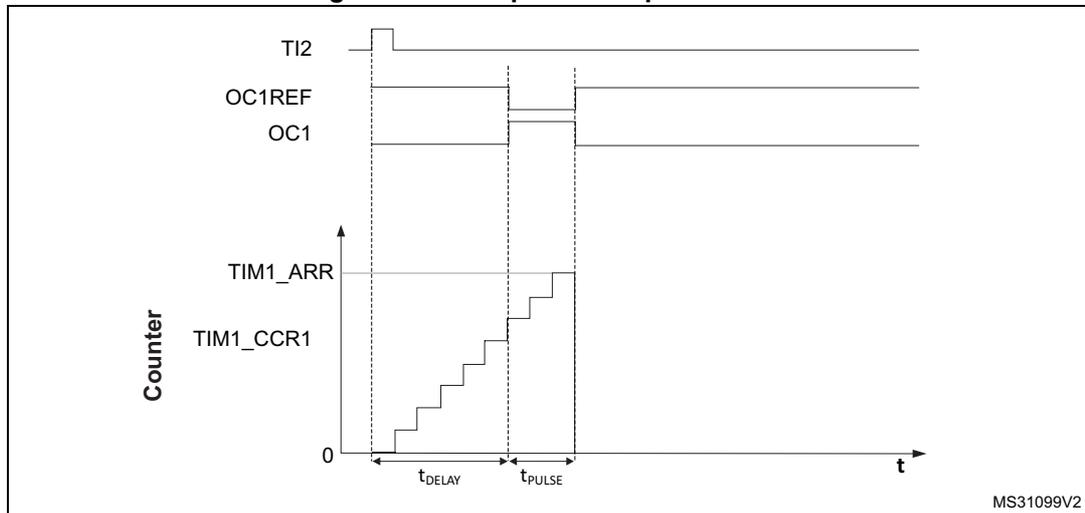
For example the user may want to generate a positive pulse on OC1 with a length of \( t_{PULSE} \) and after a delay of \( t_{DELAY} \) as soon as a positive edge is detected on the TI2 input pin.
Let's use TI2FP2 as trigger 1:
- • Map TI2FP2 to TI2 by writing CC2S='01' in the TIMx_CCMR1 register.
- • TI2FP2 must detect a rising edge, write CC2P='0' and CC2NP='0' in the TIMx_CCER register.
- • Configure TI2FP2 as trigger for the slave mode controller (TRGI) by writing TS='110' in the TIMx_SMCR register.
- • TI2FP2 is used to start the counter by writing SMS to '110' in the TIMx_SMCR register (trigger mode).
The OPM waveform is defined by writing the compare registers (taking into account the clock frequency and the counter prescaler).
- • The \( t_{\text{DELAY}} \) is defined by the value written in the TIMx_CCR1 register.
- • The \( t_{\text{PULSE}} \) is defined by the difference between the auto-reload value and the compare value (TIMx_ARR - TIMx_CCR1).
- • Let us say the user wants to build a waveform with a transition from '0' to '1' when a compare match occurs and a transition from '1' to '0' when the counter reaches the auto-reload value. To do this, enable PWM mode 2 by writing OC1M=111 in the TIMx_CCMR1 register. The user can optionally enable the preload registers by writing OC1PE='1' in the TIMx_CCMR1 register and ARPE in the TIMx_CR1 register. In this case the compare value must be written in the TIMx_CCR1 register, the auto-reload value in the TIMx_ARR register, generate an update by setting the UG bit and wait for external trigger event on TI2. CC1P is written to '0' in this example.
In our example, the DIR and CMS bits in the TIMx_CR1 register should be low.
The user only wants one pulse (Single mode), so '1' must be written in the OPM bit in the TIMx_CR1 register to stop the counter at the next update event (when the counter rolls over from the auto-reload value back to 0). When OPM bit in the TIMx_CR1 register is set to '0', so the Repetitive mode is selected.
Particular case: OCx fast enable:
In One-pulse mode, the edge detection on TIx input set the CEN bit which enables the counter. Then the comparison between the counter and the compare value makes the output toggle. But several clock cycles are needed for these operations and it limits the minimum delay \( t_{\text{DELAY min}} \) we can get.
If the user wants to output a waveform with the minimum delay, the OCxFE bit in the TIMx_CCMRx register must be set. Then OCxRef (and OCx) are forced in response to the stimulus, without taking in account the comparison. Its new level is the same as if a compare match had occurred. OCxFE acts only if the channel is configured in PWM1 or PWM2 mode.
12.3.16 Encoder interface mode
To select Encoder Interface mode write SMS='001' in the TIMx_SMCR register if the counter is counting on TI2 edges only, SMS='010' if it is counting on TI1 edges only and SMS='011' if it is counting on both TI1 and TI2 edges.
Select the TI1 and TI2 polarity by programming the CC1P and CC2P bits in the TIMx_CCER register. When needed, the user can program the input filter as well. CC1NP and CC2NP must be kept low.
The two inputs TI1 and TI2 are used to interface to an incremental encoder. Refer to Table 48 . The counter is clocked by each valid transition on TI1FP1 or TI2FP2 (TI1 and TI2 after input filter and polarity selection, TI1FP1=TI1 if not filtered and not inverted, TI2FP2=TI2 if not filtered and not inverted) assuming that it is enabled (CEN bit in TIMx_CR1 register written to '1'). The sequence of transitions of the two inputs is evaluated and generates count pulses as well as the direction signal. Depending on the sequence the counter counts up or down, the DIR bit in the TIMx_CR1 register is modified by hardware accordingly. The DIR bit is calculated at each transition on any input (TI1 or TI2), whatever the counter is counting on TI1 only, TI2 only or both TI1 and TI2.
Encoder interface mode acts simply as an external clock with direction selection. This means that the counter just counts continuously between 0 and the auto-reload value in the
TIMx_ARR register (0 to ARR or ARR down to 0 depending on the direction). So user must configure TIMx_ARR before starting. In the same way, the capture, compare, prescaler, repetition counter, trigger output features continue to work as normal. Encoder mode and External clock mode 2 are not compatible and must not be selected together.
In this mode, the counter is modified automatically following the speed and the direction of the incremental encoder and its content, therefore, always represents the encoder's position. The count direction corresponds to the rotation direction of the connected sensor. Table 48 summarizes the possible combinations, assuming TI1 and TI2 do not switch at the same time.
Table 48. Counting direction versus encoder signals
| Active edge | Level on opposite signal (TI1FP1 for TI2, TI2FP2 for TI1) | TI1FP1 signal | TI2FP2 signal | ||
|---|---|---|---|---|---|
| Rising | Falling | Rising | Falling | ||
| Counting on TI1 only | High | Down | Up | No Count | No Count |
| Low | Up | Down | No Count | No Count | |
| Counting on TI2 only | High | No Count | No Count | Up | Down |
| Low | No Count | No Count | Down | Up | |
| Counting on TI1 and TI2 | High | Down | Up | Up | Down |
| Low | Up | Down | Down | Up | |
An external incremental encoder can be connected directly to the MCU without external interface logic. However, comparators are normally used to convert the encoder's differential outputs to digital signals. This greatly increases noise immunity. The third encoder output which indicates the mechanical zero position, may be connected to an external interrupt input and trigger a counter reset.
Figure 80 gives an example of counter operation, showing count signal generation and direction control. It also shows how input jitter is compensated where both edges are selected. This might occur if the sensor is positioned near to one of the switching points. For this example we assume that the configuration is the following:
- • CC1S='01' (TIMx_CCMR1 register, TI1FP1 mapped on TI1).
- • CC2S='01' (TIMx_CCMR1 register, TI1FP2 mapped on TI2).
- • CC1P='0', CC1NP='0', and IC1F = '0000' (TIMx_CCER register, TI1FP1 non-inverted, TI1FP1=TI1).
- • CC2P='0', CC2NP='0', and IC2F = '0000' (TIMx_CCER register, TI1FP2 non-inverted, TI1FP2=TI2).
- • SMS='011' (TIMx_SMCR register, both inputs are active on both rising and falling edges).
- • CEN='1' (TIMx_CR1 register, Counter enabled).
Figure 81 gives an example of counter behavior when TI1FP1 polarity is inverted (same configuration as above except CC1P='1').
Figure 81. Example of encoder interface mode with TI1FP1 polarity inverted
The timer, when configured in Encoder Interface mode provides information on the sensor's current position. The user can obtain dynamic information (speed, acceleration, deceleration) by measuring the period between two encoder events using a second timer configured in capture mode. The output of the encoder which indicates the mechanical zero can be used for this purpose. Depending on the time between two events, the counter can also be read at regular times. This can be done by latching the counter value into a third input capture register if available (then the capture signal must be periodic and can be generated by another timer). When available, it is also possible to read its value through a DMA request generated by a real-time clock.
12.3.17 Timer input XOR function
The TI1S bit in the TIMx_CR2 register, allows the input filter of channel 1 to be connected to the output of a XOR gate, combining the three input pins TIMx_CH1, TIMx_CH2 and TIMx_CH3.
The XOR output can be used with all the timer input functions such as trigger or input capture. An example of this feature used to interface Hall sensors is given in Section 12.3.18 .
12.3.18 Interfacing with Hall sensors
This is done using the advanced-control timers (TIM1) to generate PWM signals to drive the motor and another timer TIMx (TIM2, TIM3, TIM4 or TIM5) referred to as “interfacing timer” in Figure 82 . The “interfacing timer” captures the 3 timer input pins (TIMx_CH1, TIMx_CH2, and TIMx_CH3) connected through a XOR to the TI1 input channel (selected by setting the TI1S bit in the TIMx_CR2 register).
The slave mode controller is configured in reset mode; the slave input is TI1F_ED. Thus, each time one of the 3 inputs toggles, the counter restarts counting from 0. This creates a time base triggered by any change on the Hall inputs.
On the “interfacing timer”, capture/compare channel 1 is configured in capture mode, capture signal is TRC (see Figure 65 ). The captured value, which corresponds to the time elapsed between 2 changes on the inputs, gives information about motor speed.
The “interfacing timer” can be used in output mode to generate a pulse which changes the configuration of the channels of the advanced-control timer (TIM1) (by triggering a COM event). The TIM1 timer is used to generate PWM signals to drive the motor. To do this, the interfacing timer channel must be programmed so that a positive pulse is generated after a programmed delay (in output compare or PWM mode). This pulse is sent to the advanced-control timer (TIM1) through the TRGO output.
Example: the user wants to change the PWM configuration of the advanced-control timer TIM1 after a programmed delay each time a change occurs on the Hall inputs connected to one of the TIMx timers.
- • Configure 3 timer inputs ORed to the TI1 input channel by writing the TI1S bit in the TIMx_CR2 register to ‘1’,
- • Program the time base: write the TIMx_ARR to the max value (the counter must be cleared by the TI1 change. Set the prescaler to get a maximum counter period longer than the time between 2 changes on the sensors,
- • Program channel 1 in capture mode (TRC selected): write the CC1S bits in the TIMx_CCMR1 register to ‘11’. The user can also program the digital filter if needed,
- • Program channel 2 in PWM 2 mode with the desired delay: write the OC2M bits to ‘111’ and the CC2S bits to ‘00’ in the TIMx_CCMR1 register,
- • Select OC2REF as trigger output on TRGO: write the MMS bits in the TIMx_CR2 register to ‘101’,
In the advanced-control timer TIM1, the right ITR input must be selected as trigger input, the timer is programmed to generate PWM signals, the capture/compare control signals are preloaded (CCPC=1 in the TIMx_CR2 register) and the COM event is controlled by the trigger input (CCUS=1 in the TIMx_CR2 register). The PWM control bits (CCxE, OCxM) are written after a COM event for the next step (this can be done in an interrupt subroutine generated by the rising edge of OC2REF).
Figure 82 describes this example.
Figure 82. Example of Hall sensor interface
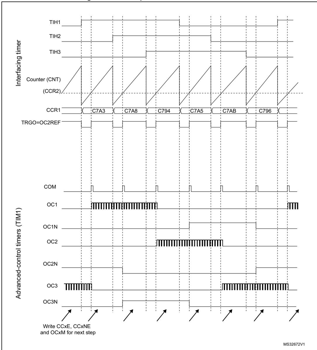
The timing diagram illustrates the interaction between an Interfacing timer and Advanced-control timers (TIM1) for a Hall sensor interface. The diagram is divided into two main sections: Interfacing timer and Advanced-control timers (TIM1).
Interfacing timer signals:
- TIH1, TIH2, TIH3: Hall sensor inputs. TIH1 and TIH2 show transitions that trigger the counter. TIH3 is shown as a constant high level.
- Counter (CNT) (CCR2): A sawtooth waveform representing the counter value, starting at 0 and increasing until it reaches the CCR2 register value, then resetting.
- CCR1: Capture/Compare Register 1. It contains a sequence of values: C7A3, C7A8, C794, C7A5, C7AB, C796. These values are captured when the counter matches the register value.
- TRGO=OC2REF: A periodic square wave output generated by the timer.
Advanced-control timers (TIM1) signals:
- COM: Common output signal, which pulses briefly at the start of each counter cycle.
- OC1: Output Compare 1. It is a PWM signal that is active (high-frequency oscillation) during the first half of the counter cycle (from 0 to C7A8).
- OC1N: Inverted Output Compare 1. It is low during the first half of the counter cycle and high otherwise.
- OC2: Output Compare 2. It is a PWM signal that is active during the second half of the counter cycle (from C7A8 to C7AB).
- OC2N: Inverted Output Compare 2. It is low during the second half of the counter cycle and high otherwise.
- OC3: Output Compare 3. It is a PWM signal that is active from the start of the cycle until the first capture (CCR1 = C7A3) and from the last capture (CCR1 = C7AB) until the end of the cycle.
- OC3N: Inverted Output Compare 3. It is low during the active periods of OC3 and high otherwise.
Annotations:
- Arrows at the bottom point to the rising edges of the TRGO=OC2REF signal, labeled "Write CCxE, CCxNE and OCxM for next step", indicating that the timer configuration should be updated at these points.
- The identifier "MS32672V1" is located in the bottom right corner of the diagram.
12.3.19 TIMx and external trigger synchronization
The TIMx timer can be synchronized with an external trigger in several modes: Reset mode, Gated mode and Trigger mode.
Slave mode: Reset mode
The counter and its prescaler can be reinitialized in response to an event on a trigger input. Moreover, if the URS bit from the TIMx_CR1 register is low, an update event UEV is generated. Then all the preloaded registers (TIMx_ARR, TIMx_CCRx) are updated.
In the following example, the upcounter is cleared in response to a rising edge on TI1 input:
- • Configure the channel 1 to detect rising edges on TI1. Configure the input filter duration (in this example, we don't need any filter, so we keep IC1F=0000). The capture prescaler is not used for triggering, so there's no need to configure it. The CC1S bits select the input capture source only, CC1S = 01 in the TIMx_CCMR1 register. Write CC1P=0 and CC1NP='0' in TIMx_CCER register to validate the polarity (and detect rising edges only).
- • Configure the timer in reset mode by writing SMS=100 in TIMx_SMCR register. Select TI1 as the input source by writing TS=101 in TIMx_SMCR register.
- • Start the counter by writing CEN=1 in the TIMx_CR1 register.
The counter starts counting on the internal clock, then behaves normally until TI1 rising edge. When TI1 rises, the counter is cleared and restarts from 0. In the meantime, the trigger flag is set (TIF bit in the TIMx_SR register) and an interrupt request, or a DMA request can be sent if enabled (depending on the TIE and TDE bits in TIMx_DIER register).
The following figure shows this behavior when the auto-reload register TIMx_ARR=0x36. The delay between the rising edge on TI1 and the actual reset of the counter is due to the resynchronization circuit on TI1 input.
Figure 83. Control circuit in reset mode
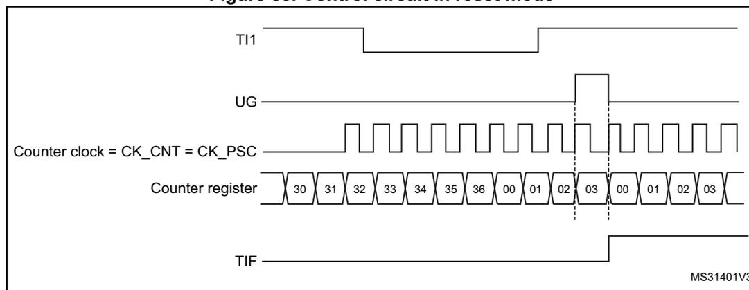
Timing diagram showing the control circuit in reset mode. The diagram illustrates the relationship between the TI1 input, the UG (Update Generation) signal, the Counter clock (CK_CNT = CK_PSC), the Counter register values, and the TIF (Trigger Interrupt Flag) signal. The TI1 input is shown as a rising edge. The UG signal is a pulse that goes high when the TI1 input rises. The Counter clock is a periodic square wave. The Counter register values are shown as a sequence of numbers: 30, 31, 32, 33, 34, 35, 36, 00, 01, 02, 03, 00, 01, 02, 03. The counter resets to 00 when the TI1 input rises. The TIF signal is a pulse that goes high when the counter resets. The diagram is labeled MS31401V3 in the bottom right corner.
Slave mode: Gated mode
The counter can be enabled depending on the level of a selected input.
In the following example, the upcounter counts only when TI1 input is low:
- • Configure the channel 1 to detect low levels on TI1. Configure the input filter duration (in this example, we don't need any filter, so we keep IC1F=0000). The capture prescaler is not used for triggering, so the user does not need to configure it. The CC1S bits select the input capture source only, CC1S=01 in TIMx_CCMR1 register. Write CC1P=1 and CC1NP='0' in TIMx_CCER register to validate the polarity (and detect low level only).
- • Configure the timer in gated mode by writing SMS=101 in TIMx_SMCR register. Select TI1 as the input source by writing TS=101 in TIMx_SMCR register.
- • Enable the counter by writing CEN=1 in the TIMx_CR1 register (in gated mode, the counter doesn't start if CEN=0, whatever is the trigger input level).
The counter starts counting on the internal clock as long as TI1 is low and stops as soon as TI1 becomes high. The TIF flag in the TIMx_SR register is set both when the counter starts or stops.
The delay between the rising edge on TI1 and the actual stop of the counter is due to the resynchronization circuit on TI1 input.
Figure 84. Control circuit in gated mode
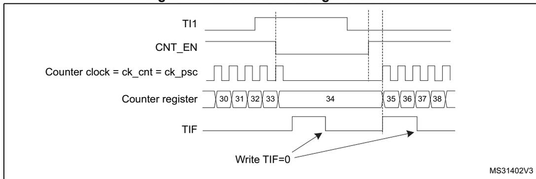
Slave mode: Trigger mode
The counter can start in response to an event on a selected input.
In the following example, the upcounter starts in response to a rising edge on TI2 input:
- • Configure the channel 2 to detect rising edges on TI2. Configure the input filter duration (in this example, we don't need any filter, so we keep IC2F=0000). The capture prescaler is not used for triggering, so there's no need to configure it. The CC2S bits are configured to select the input capture source only, CC2S=01 in TIMx_CCMR1 register. Write CC2P=1 and CC2NP=0 in TIMx_CCER register to validate the polarity (and detect low level only).
- • Configure the timer in trigger mode by writing SMS=110 in TIMx_SMCR register. Select TI2 as the input source by writing TS=110 in TIMx_SMCR register.
When a rising edge occurs on TI2, the counter starts counting on the internal clock and the TIF flag is set.
The delay between the rising edge on TI2 and the actual start of the counter is due to the resynchronization circuit on TI2 input.
Figure 85. Control circuit in trigger mode
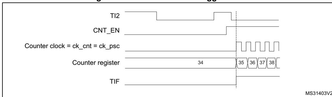
Slave mode: external clock mode 2 + trigger mode
The external clock mode 2 can be used in addition to another slave mode (except external clock mode 1 and encoder mode). In this case, the ETR signal is used as external clock input, and another input can be selected as trigger input (in reset mode, gated mode or trigger mode). It is recommended not to select ETR as TRGI through the TS bits of TIMx_SMCR register.
In the following example, the upcounter is incremented at each rising edge of the ETR signal as soon as a rising edge of TI1 occurs:
- Configure the external trigger input circuit by programming the TIMx_SMCR register as follows:
- – ETF = 0000: no filter
- – ETPS = 00: prescaler disabled
- – ETP = 0: detection of rising edges on ETR and ECE=1 to enable the external clock mode 2.
- Configure the channel 1 as follows, to detect rising edges on TI:
- – IC1F=0000: no filter.
- – The capture prescaler is not used for triggering and does not need to be configured.
- – CC1S=01 in TIMx_CCMR1 register to select only the input capture source
- – CC1P=0 and CC1NP='0' in TIMx_CCER register to validate the polarity (and detect rising edge only).
- Configure the timer in trigger mode by writing SMS=110 in TIMx_SMCR register. Select TI1 as the input source by writing TS=101 in TIMx_SMCR register.
A rising edge on TI1 enables the counter and sets the TIF flag. The counter then counts on ETR rising edges.
The delay between the rising edge of the ETR signal and the actual reset of the counter is due to the resynchronization circuit on ETRP input.
Figure 86. Control circuit in external clock mode 2 + trigger mode
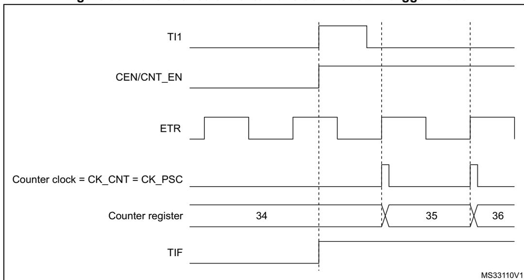
The timing diagram shows the following signals and their relationship:
- TI1 : A signal that goes high at the start and then low.
- CEN/CNT_EN : A signal that goes high at the start and remains high.
- ETR : An external trigger signal that is a periodic square wave.
- Counter clock = CK_CNT = CK_PSC : A signal that is initially low and then becomes a periodic square wave, with its rising edges synchronized with the falling edges of the ETR signal.
- Counter register : A register that increments its value (34, 35, 36) on the rising edges of the counter clock signal.
- TIF : A signal that goes high at the start and remains high.
The diagram is labeled MS33110V1.
12.3.20 Timer synchronization
The TIM timers are linked together internally for timer synchronization or chaining. Refer to Section 13.3.15: Timer synchronization for details.
Note: The clock of the slave timer must be enabled prior to receive events from the master timer, and must not be changed on-the-fly while triggers are received from the master timer.
12.3.21 Debug mode
When the microcontroller enters debug mode (Cortex®-M4 with FPU core halted), the TIMx counter either continues to work normally or stops, depending on DBG_TIMx_STOP configuration bit in DBG module. For more details, refer to Section 23.16.2: Debug support for timers, watchdog and I 2 C .
For safety purposes, when the counter is stopped (DBG_TIMx_STOP = 1 in DBGMCU_APBx_FZ register), the outputs are disabled (as if the MOE bit was reset). The outputs can either be forced to an inactive state (OSSI bit = 1), or have their control taken over by the GPIO controller (OSSI bit = 0) to force them to Hi-Z.
12.4 TIM1 registers
Refer to Section 2.2 for a list of abbreviations used in register descriptions.
The peripheral registers must be written by half-words (16 bits) or words (32 bits). Read accesses can be done by bytes (8 bits), half-word (16 bits) or words (32 bits).
12.4.1 TIM1 control register 1 (TIMx_CR1)
Address offset: 0x00
Reset value: 0x0000
| 15 | 14 | 13 | 12 | 11 | 10 | 9 | 8 | 7 | 6 | 5 | 4 | 3 | 2 | 1 | 0 |
|---|---|---|---|---|---|---|---|---|---|---|---|---|---|---|---|
| Reserved | CKD[1:0] | ARPE | CMS[1:0] | DIR | OPM | URS | UDIS | CEN | |||||||
| rw | rw | rw | rw | rw | rw | rw | rw | rw | rw | ||||||
Bits 15:10 Reserved, must be kept at reset value.
Bits 9:8 CKD[1:0] : Clock division
This bit-field indicates the division ratio between the timer clock (CK_INT) frequency and the dead-time and sampling clock ( \( t_{DTS} \) ) used by the dead-time generators and the digital filters (ETR, TIx),
00: \( t_{DTS}=t_{CK\_INT} \)
01: \( t_{DTS}=2*t_{CK\_INT} \)
10: \( t_{DTS}=4*t_{CK\_INT} \)
11: Reserved, do not program this value
Bit 7 ARPE : Auto-reload preload enable
0: TIMx_ARR register is not buffered
1: TIMx_ARR register is buffered
Bits 6:5 CMS[1:0] : Center-aligned mode selection
00: Edge-aligned mode. The counter counts up or down depending on the direction bit (DIR).
01: Center-aligned mode 1. The counter counts up and down alternatively. Output compare interrupt flags of channels configured in output (CCxS=00 in TIMx_CCMRx register) are set only when the counter is counting down.
10: Center-aligned mode 2. The counter counts up and down alternatively. Output compare interrupt flags of channels configured in output (CCxS=00 in TIMx_CCMRx register) are set only when the counter is counting up.
11: Center-aligned mode 3. The counter counts up and down alternatively. Output compare interrupt flags of channels configured in output (CCxS=00 in TIMx_CCMRx register) are set both when the counter is counting up or down.
Note: It is not allowed to switch from edge-aligned mode to center-aligned mode as long as the counter is enabled (CEN=1)
Bit 4 DIR : Direction
0: Counter used as upcounter
1: Counter used as downcounter
Note: This bit is read only when the timer is configured in Center-aligned mode or Encoder mode.
Bit 3 OPM : One pulse mode
0: Counter is not stopped at update event
1: Counter stops counting at the next update event (clearing the bit CEN)
Bit 2 URS : Update request source
This bit is set and cleared by software to select the UEV event sources.
0: Any of the following events generate an update interrupt or DMA request if enabled.
These events can be:
- – Counter overflow/underflow
- – Setting the UG bit
- – Update generation through the slave mode controller
1: Only counter overflow/underflow generates an update interrupt or DMA request if enabled.
Bit 1 UDIS : Update disable
This bit is set and cleared by software to enable/disable UEV event generation.
0: UEV enabled. The Update (UEV) event is generated by one of the following events:
- – Counter overflow/underflow
- – Setting the UG bit
- – Update generation through the slave mode controller
Buffered registers are then loaded with their preload values.
1: UEV disabled. The Update event is not generated, shadow registers keep their value (ARR, PSC, CCRx). However the counter and the prescaler are reinitialized if the UG bit is set or if a hardware reset is received from the slave mode controller.
Bit 0 CEN : Counter enable
0: Counter disabled
1: Counter enabled
Note: External clock, gated mode and encoder mode can work only if the CEN bit has been previously set by software. However trigger mode can set the CEN bit automatically by hardware.
12.4.2 TIM1 control register 2 (TIMx_CR2)
Address offset: 0x04
Reset value: 0x0000
| 15 | 14 | 13 | 12 | 11 | 10 | 9 | 8 | 7 | 6 | 5 | 4 | 3 | 2 | 1 | 0 |
|---|---|---|---|---|---|---|---|---|---|---|---|---|---|---|---|
| Res. | OIS4 | OIS3N | OIS3 | OIS2N | OIS2 | OIS1N | OIS1 | TI1S | MMS[2:0] | CCDS | CCUS | Res. | CCPC | ||
| rw | rw | rw | rw | rw | rw | rw | rw | rw | rw | rw | rw | rw | rw | ||
Bit 15 Reserved, must be kept at reset value.
Bit 14
OIS4
: Output Idle state 4 (OC4 output)
refer to OIS1 bit
Bit 13
OIS3N
: Output Idle state 3 (OC3N output)
refer to OIS1N bit
Bit 12
OIS3
: Output Idle state 3 (OC3 output)
refer to OIS1 bit
Bit 11
OIS2N
: Output Idle state 2 (OC2N output)
refer to OIS1N bit
Bit 10
OIS2
: Output Idle state 2 (OC2 output)
refer to OIS1 bit
Bit 9 OIS1N : Output Idle state 1 (OC1N output)
0: OC1N=0 after a dead-time when MOE=0
1: OC1N=1 after a dead-time when MOE=0
Note: This bit can not be modified as long as LOCK level 1, 2 or 3 has been programmed (LOCK bits in TIMx_BDTR register).
Bit 8 OIS1 : Output Idle state 1 (OC1 output)
0: OC1=0 (after a dead-time if OC1N is implemented) when MOE=0
1: OC1=1 (after a dead-time if OC1N is implemented) when MOE=0
Note: This bit can not be modified as long as LOCK level 1, 2 or 3 has been programmed (LOCK bits in TIMx_BDTR register).
Bit 7 TI1S : TI1 selection
0: The TIMx_CH1 pin is connected to TI1 input
1: The TIMx_CH1, CH2 and CH3 pins are connected to the TI1 input (XOR combination)
Bits 6:4 MMS[2:0] : Master mode selection
These bits allow to select the information to be sent in master mode to slave timers for synchronization (TRGO). The combination is as follows:
000: Reset - the UG bit from the TIMx_EGR register is used as trigger output (TRGO). If the reset is generated by the trigger input (slave mode controller configured in reset mode) then the signal on TRGO is delayed compared to the actual reset.
001: Enable - the Counter Enable signal CNT_EN is used as trigger output (TRGO). It is useful to start several timers at the same time or to control a window in which a slave timer is enable. The Counter Enable signal is generated by a logic OR between CEN control bit and the trigger input when configured in gated mode. When the Counter Enable signal is controlled by the trigger input, there is a delay on TRGO, except if the master/slave mode is selected (see the MSM bit description in TIMx_SMCR register).
010: Update - The update event is selected as trigger output (TRGO). For instance a master timer can then be used as a prescaler for a slave timer.
011: Compare Pulse - The trigger output send a positive pulse when the CC1IF flag is to be set (even if it was already high), as soon as a capture or a compare match occurred. (TRGO).
100: Compare - OC1REF signal is used as trigger output (TRGO)
101: Compare - OC2REF signal is used as trigger output (TRGO)
110: Compare - OC3REF signal is used as trigger output (TRGO)
111: Compare - OC4REF signal is used as trigger output (TRGO)
Note: The clock of the slave timer and ADC must be enabled prior to receiving events from the master timer, and must not be changed on-the-fly while triggers are received from the master timer.
Bit 3 CCDS : Capture/compare DMA selection
0: CCx DMA request sent when CCx event occurs
1: CCx DMA requests sent when update event occurs
Bit 2 CCUS : Capture/compare control update selection
0: When capture/compare control bits are preloaded (CCPC=1), they are updated by setting the COMG bit only
1: When capture/compare control bits are preloaded (CCPC=1), they are updated by setting the COMG bit or when an rising edge occurs on TRGI
Note: This bit acts only on channels that have a complementary output.
Bit 1 Reserved, must be kept at reset value.
Bit 0 CCPC : Capture/compare preloaded control
0: CCxE, CCxNE and OCxM bits are not preloaded
1: CCxE, CCxNE and OCxM bits are preloaded, after having been written, they are updated only when a commutation event (COM) occurs (COMG bit set or rising edge detected on TRGI, depending on the CCUS bit).
Note: This bit acts only on channels that have a complementary output.
12.4.3 TIM1 slave mode control register (TIMx_SMCR)
Address offset: 0x08
Reset value: 0x0000
| 15 | 14 | 13 | 12 | 11 | 10 | 9 | 8 | 7 | 6 | 5 | 4 | 3 | 2 | 1 | 0 |
|---|---|---|---|---|---|---|---|---|---|---|---|---|---|---|---|
| ETP | ECE | ETPS[1:0] | ETF[3:0] | MSM | TS[2:0] | Res. | SMS[2:0] | ||||||||
| rw | rw | rw | rw | rw | rw | rw | rw | rw | rw | rw | rw | Res. | rw | rw | rw |
Bit 15 ETP : External trigger polarity
This bit selects whether ETR or ETR is used for trigger operations
0: ETR is non-inverted, active at high level or rising edge.
1: ETR is inverted, active at low level or falling edge.
Bit 14 ECE : External clock enable
This bit enables External clock mode 2.
0: External clock mode 2 disabled
1: External clock mode 2 enabled. The counter is clocked by any active edge on the ETRF signal.
Note: 1: Setting the ECE bit has the same effect as selecting external clock mode 1 with TRGI connected to ETRF (SMS=111 and TS=111).
2: It is possible to simultaneously use external clock mode 2 with the following slave modes: reset mode, gated mode and trigger mode. Nevertheless, TRGI must not be connected to ETRF in this case (TS bits must not be 111).
3: If external clock mode 1 and external clock mode 2 are enabled at the same time, the external clock input is ETRF.
Bits 13:12 ETPS[1:0] : External trigger prescaler
External trigger signal ETRP frequency must be at most 1/4 of TIMxCLK frequency. A prescaler can be enabled to reduce ETRP frequency. It is useful when inputting fast external clocks.
00: Prescaler OFF
01: ETRP frequency divided by 2
10: ETRP frequency divided by 4
11: ETRP frequency divided by 8
Bits 11:8 ETF[3:0] : External trigger filterThis bit-field then defines the frequency used to sample ETRP signal and the length of the digital filter applied to ETRP. The digital filter is made of an event counter in which N consecutive events are needed to validate a transition on the output:
0000: No filter, sampling is done at \( f_{DTS} \)
0001: \( f_{SAMPLING}=f_{CK\_INT} \) , N=2
0010: \( f_{SAMPLING}=f_{CK\_INT} \) , N=4
0011: \( f_{SAMPLING}=f_{CK\_INT} \) , N=8
0100: \( f_{SAMPLING}=f_{DTS}/2 \) , N=6
0101: \( f_{SAMPLING}=f_{DTS}/2 \) , N=8
0110: \( f_{SAMPLING}=f_{DTS}/4 \) , N=6
0111: \( f_{SAMPLING}=f_{DTS}/4 \) , N=8
1000: \( f_{SAMPLING}=f_{DTS}/8 \) , N=6
1001: \( f_{SAMPLING}=f_{DTS}/8 \) , N=8
1010: \( f_{SAMPLING}=f_{DTS}/16 \) , N=5
1011: \( f_{SAMPLING}=f_{DTS}/16 \) , N=6
1100: \( f_{SAMPLING}=f_{DTS}/16 \) , N=8
1101: \( f_{SAMPLING}=f_{DTS}/32 \) , N=5
1110: \( f_{SAMPLING}=f_{DTS}/32 \) , N=6
1111: \( f_{SAMPLING}=f_{DTS}/32 \) , N=8
Bit 7 MSM : Master/slave mode0: No action
1: The effect of an event on the trigger input (TRGI) is delayed to allow a perfect synchronization between the current timer and its slaves (through TRGO). It is useful if we want to synchronize several timers on a single external event.
Bits 6:4 TS[2:0] : Trigger selectionThis bit-field selects the trigger input to be used to synchronize the counter.
000: Internal Trigger 0 (ITR0)
001: Internal Trigger 1 (ITR1)
010: Internal Trigger 2 (ITR2)
011: Internal Trigger 3 (ITR3)
100: TI1 Edge Detector (TI1F_ED)
101: Filtered Timer Input 1 (TI1FP1)
110: Filtered Timer Input 2 (TI2FP2)
111: External Trigger input (ETRF)
See Table 49 for more details on ITRx meaning for each Timer.
Note: These bits must be changed only when they are not used (e.g. when SMS=000) to avoid wrong edge detections at the transition.
Bit 3 Reserved, must be kept at reset value.
Bits 2:0 SMS : Slave mode selection
When external signals are selected the active edge of the trigger signal (TRGI) is linked to the polarity selected on the external input (see Input Control register and Control register description.
000: Slave mode disabled - if CEN = '1' then the prescaler is clocked directly by the internal clock.
001: Encoder mode 1 - Counter counts up/down on TI1FP1 edge depending on TI2FP2 level.
010: Encoder mode 2 - Counter counts up/down on TI2FP2 edge depending on TI1FP1 level.
011: Encoder mode 3 - Counter counts up/down on both TI1FP1 and TI2FP2 edges depending on the level of the other input.
100: Reset mode - Rising edge of the selected trigger input (TRGI) reinitializes the counter and generates an update of the registers.
101: Gated mode - The counter clock is enabled when the trigger input (TRGI) is high. The counter stops (but is not reset) as soon as the trigger becomes low. Both start and stop of the counter are controlled.
110: Trigger mode - The counter starts at a rising edge of the trigger TRGI (but it is not reset). Only the start of the counter is controlled.
111: External Clock mode 1 - Rising edges of the selected trigger (TRGI) clock the counter.
Note: The gated mode must not be used if TI1F_ED is selected as the trigger input (TS='100'). Indeed, TI1F_ED outputs 1 pulse for each transition on TI1F, whereas the gated mode checks the level of the trigger signal.
The clock of the slave timer must be enabled prior to receiving events from the master timer, and must not be changed on-the-fly while triggers are received from the master timer.
Table 49. TIMx Internal trigger connection
| Slave TIM | ITR0 (TS = 000) | ITR1 (TS = 001) | ITR2 (TS = 010) | ITR3 (TS = 011) |
|---|---|---|---|---|
| TIM1 | TIM5_TRGO | TIM2_TRGO | TIM3_TRGO | TIM4_TRGO |
12.4.4 TIM1 DMA/interrupt enable register (TIMx_DIER)
Address offset: 0x0C
Reset value: 0x0000
| 15 | 14 | 13 | 12 | 11 | 10 | 9 | 8 | 7 | 6 | 5 | 4 | 3 | 2 | 1 | 0 |
|---|---|---|---|---|---|---|---|---|---|---|---|---|---|---|---|
| Res. | TDE | COMDE | CC4DE | CC3DE | CC2DE | CC1DE | UDE | BIE | TIE | COMIE | CC4IE | CC3IE | CC2IE | CC1IE | UIE |
| rw | rw | rw | rw | rw | rw | rw | rw | rw | rw | rw | rw | rw | rw | rw |
Bit 15 Reserved, must be kept at reset value.
Bit 14 TDE : Trigger DMA request enable
- 0: Trigger DMA request disabled
- 1: Trigger DMA request enabled
Bit 13 COMDE : COM DMA request enable
- 0: COM DMA request disabled
- 1: COM DMA request enabled

- Bit 12
CC4DE
: Capture/Compare 4 DMA request enable
0: CC4 DMA request disabled
1: CC4 DMA request enabled - Bit 11
CC3DE
: Capture/Compare 3 DMA request enable
0: CC3 DMA request disabled
1: CC3 DMA request enabled - Bit 10
CC2DE
: Capture/Compare 2 DMA request enable
0: CC2 DMA request disabled
1: CC2 DMA request enabled - Bit 9
CC1DE
: Capture/Compare 1 DMA request enable
0: CC1 DMA request disabled
1: CC1 DMA request enabled - Bit 8
UDE
: Update DMA request enable
0: Update DMA request disabled
1: Update DMA request enabled - Bit 7
BIE
: Break interrupt enable
0: Break interrupt disabled
1: Break interrupt enabled - Bit 6
TIE
: Trigger interrupt enable
0: Trigger interrupt disabled
1: Trigger interrupt enabled - Bit 5
COMIE
: COM interrupt enable
0: COM interrupt disabled
1: COM interrupt enabled - Bit 4
CC4IE
: Capture/Compare 4 interrupt enable
0: CC4 interrupt disabled
1: CC4 interrupt enabled - Bit 3
CC3IE
: Capture/Compare 3 interrupt enable
0: CC3 interrupt disabled
1: CC3 interrupt enabled - Bit 2
CC2IE
: Capture/Compare 2 interrupt enable
0: CC2 interrupt disabled
1: CC2 interrupt enabled - Bit 1
CC1IE
: Capture/Compare 1 interrupt enable
0: CC1 interrupt disabled
1: CC1 interrupt enabled - Bit 0
UIE
: Update interrupt enable
0: Update interrupt disabled
1: Update interrupt enabled
12.4.5 TIM1 status register (TIMx_SR)
Address offset: 0x10
Reset value: 0x0000
| 15 | 14 | 13 | 12 | 11 | 10 | 9 | 8 | 7 | 6 | 5 | 4 | 3 | 2 | 1 | 0 |
|---|---|---|---|---|---|---|---|---|---|---|---|---|---|---|---|
| Reserved | CC4OF | CC3OF | CC2OF | CC1OF | Res. | BIF | TIF | COMIF | CC4IF | CC3IF | CC2IF | CC1IF | UIF | ||
| rc_w0 | rc_w0 | rc_w0 | rc_w0 | Res. | rc_w0 | rc_w0 | rc_w0 | rc_w0 | rc_w0 | rc_w0 | rc_w0 | rc_w0 | |||
Bits 15:13 Reserved, must be kept at reset value.
Bit 12
CC4OF
: Capture/Compare 4 overcapture flag
refer to CC1OF description
Bit 11
CC3OF
: Capture/Compare 3 overcapture flag
refer to CC1OF description
Bit 10
CC2OF
: Capture/Compare 2 overcapture flag
refer to CC1OF description
Bit 9
CC1OF
: Capture/Compare 1 overcapture flag
This flag is set by hardware only when the corresponding channel is configured in input capture mode. It is cleared by software by writing it to '0'.
0: No overcapture has been detected.
1: The counter value has been captured in TIMx_CCR1 register while CC1IF flag was already set
Bit 8 Reserved, must be kept at reset value.
Bit 7
BIF
: Break interrupt flag
This flag is set by hardware as soon as the break input goes active. It can be cleared by software if the break input is not active.
0: No break event occurred.
1: An active level has been detected on the break input.
Bit 6
TIF
: Trigger interrupt flag
This flag is set by hardware on trigger event (active edge detected on TRGI input when the slave mode controller is enabled in all modes but gated mode. It is set when the counter starts or stops when gated mode is selected. It is cleared by software.
0: No trigger event occurred.
1: Trigger interrupt pending.
Bit 5
COMIF
: COM interrupt flag
This flag is set by hardware on COM event (when Capture/compare Control bits - CCxE, CCxNE, OCxM - have been updated). It is cleared by software.
0: No COM event occurred.
1: COM interrupt pending.
Bit 4
CC4IF
: Capture/Compare 4 interrupt flag
refer to CC1IF description
Bit 3
CC3IF
: Capture/Compare 3 interrupt flag
refer to CC1IF description
Bit 2
CC2IF
: Capture/Compare 2 interrupt flag
refer to CC1IF description
Bit 1 CC1IF : Capture/Compare 1 interrupt flag
If channel CC1 is configured as output:
This flag is set by hardware when the counter matches the compare value, with some exception in center-aligned mode (refer to the CMS bits in the TIMx_CR1 register description). It is cleared by software.
0: No match.
1: The content of the counter TIMx_CNT matches the content of the TIMx_CCR1 register. When the contents of TIMx_CCR1 are greater than the contents of TIMx_ARR, the CC1IF bit goes high on the counter overflow (in upcounting and up/down-counting modes) or underflow (in downcounting mode)
If channel CC1 is configured as input:
This bit is set by hardware on a capture. It is cleared by software or by reading the TIMx_CCR1 register.
0: No input capture occurred
1: The counter value has been captured in TIMx_CCR1 register (An edge has been detected on IC1 which matches the selected polarity)
Bit 0 UIF : Update interrupt flag
This bit is set by hardware on an update event. It is cleared by software.
0: No update occurred.
1: Update interrupt pending. This bit is set by hardware when the registers are updated:
- – At overflow or underflow regarding the repetition counter value (update if repetition counter = 0) and if the UDIS=0 in the TIMx_CR1 register.
- – When CNT is reinitialized by software using the UG bit in TIMx_EGR register, if URS=0 and UDIS=0 in the TIMx_CR1 register.
- – When CNT is reinitialized by a trigger event (refer to Section 12.4.3: TIM1 slave mode control register (TIMx_SMCR) ), if URS=0 and UDIS=0 in the TIMx_CR1 register.
12.4.6 TIM1 event generation register (TIMx_EGR)
Address offset: 0x14
Reset value: 0x0000
| 15 | 14 | 13 | 12 | 11 | 10 | 9 | 8 | 7 | 6 | 5 | 4 | 3 | 2 | 1 | 0 |
|---|---|---|---|---|---|---|---|---|---|---|---|---|---|---|---|
| Reserved | BG | TG | COMG | CC4G | CC3G | CC2G | CC1G | UG | |||||||
| w | w | w | w | w | w | w | w | ||||||||
Bits 15:8 Reserved, must be kept at reset value.
Bit 7 BG : Break generation
This bit is set by software in order to generate an event, it is automatically cleared by hardware.
0: No action
1: A break event is generated. MOE bit is cleared and BIF flag is set. Related interrupt or DMA transfer can occur if enabled.
Bit 6 TG : Trigger generation
This bit is set by software in order to generate an event, it is automatically cleared by hardware.
0: No action
1: The TIF flag is set in TIMx_SR register. Related interrupt or DMA transfer can occur if enabled.
Bit 5
COMG
: Capture/Compare control update generation
This bit can be set by software, it is automatically cleared by hardware
0: No action
1: When CCPC bit is set, it allows to update CCxE, CCxNE and OCxM bits
Note: This bit acts only on channels having a complementary output.
Bit 4
CC4G
: Capture/Compare 4 generation
refer to CC1G description
Bit 3
CC3G
: Capture/Compare 3 generation
refer to CC1G description
Bit 2
CC2G
: Capture/Compare 2 generation
refer to CC1G description
Bit 1
CC1G
: Capture/Compare 1 generation
This bit is set by software in order to generate an event, it is automatically cleared by hardware.
0: No action
1: A capture/compare event is generated on channel 1:
If channel CC1 is configured as output:
CC1IF flag is set, Corresponding interrupt or DMA request is sent if enabled.
If channel CC1 is configured as input:
The current value of the counter is captured in TIMx_CCR1 register. The CC1IF flag is set, the corresponding interrupt or DMA request is sent if enabled. The CC1OF flag is set if the CC1IF flag was already high.
Bit 0
UG
: Update generation
This bit can be set by software, it is automatically cleared by hardware.
0: No action
1: Reinitialize the counter and generates an update of the registers. Note that the prescaler counter is cleared too (anyway the prescaler ratio is not affected). The counter is cleared if the center-aligned mode is selected or if DIR=0 (upcounting), else it takes the auto-reload value (TIMx_ARR) if DIR=1 (downcounting).
12.4.7 TIM1 capture/compare mode register 1 (TIMx_CCMR1)
Address offset: 0x18
Reset value: 0x0000
The channels can be used in input (capture mode) or in output (compare mode). The direction of a channel is defined by configuring the corresponding CCxS bits. All the other bits of this register have a different function in input and in output mode. For a given bit, OCxx describes its function when the channel is configured in output, ICxx describes its function when the channel is configured in input. So the user must take care that the same bit can have a different meaning for the input stage and for the output stage.
| 15 | 14 | 13 | 12 | 11 | 10 | 9 | 8 | 7 | 6 | 5 | 4 | 3 | 2 | 1 | 0 |
|---|---|---|---|---|---|---|---|---|---|---|---|---|---|---|---|
| OC2CE | OC2M[2:0] | OC2PE | OC2FE | CC2S[1:0] | OC1CE | OC1M[2:0] | OC1PE | OC1FE | CC1S[1:0] | ||||||
| IC2F[3:0] | IC2PSC[1:0] | IC1F[3:0] | IC1PSC[1:0] | ||||||||||||
| rw | rw | rw | rw | rw | rw | rw | rw | rw | rw | rw | rw | rw | rw | rw | rw |
Output compare mode:
Bit 15 OC2CE : Output compare 2 clear enable
Bits 14:12 OC2M[2:0] : Output compare 2 mode
Bit 11 OC2PE : Output compare 2 preload enable
Bit 10 OC2FE : Output compare 2 fast enable
Bits 9:8 CC2S[1:0] : Capture/Compare 2 selection
This bit-field defines the direction of the channel (input/output) as well as the used input.
00: CC2 channel is configured as output
01: CC2 channel is configured as input, IC2 is mapped on TI2
10: CC2 channel is configured as input, IC2 is mapped on TI1
11: CC2 channel is configured as input, IC2 is mapped on TRC. This mode is working only if an internal trigger input is selected through the TS bit (TIMx_SMCR register)
Note: CC2S bits are writable only when the channel is OFF (CC2E = '0' in TIMx_CCER).
Bit 7 OC1CE : Output compare 1 clear enable
OC1CE: Output compare 1 Clear Enable
0: OC1Ref is not affected by the ETRF Input
1: OC1Ref is cleared as soon as a High level is detected on ETRF input
Bits 6:4 OC1M : Output compare 1 mode
These bits define the behavior of the output reference signal OC1REF from which OC1 and OC1N are derived. OC1REF is active high whereas OC1 and OC1N active level depends on CC1P and CC1NP bits.
000: Frozen - The comparison between the output compare register TIMx_CCR1 and the counter TIMx_CNT has no effect on the outputs. (this mode is used to generate a timing base).
001: Set channel 1 to active level on match. OC1REF signal is forced high when the counter TIMx_CNT matches the capture/compare register 1 (TIMx_CCR1).
010: Set channel 1 to inactive level on match. OC1REF signal is forced low when the counter TIMx_CNT matches the capture/compare register 1 (TIMx_CCR1).
011: Toggle - OC1REF toggles when TIMx_CNT=TIMx_CCR1.
100: Force inactive level - OC1REF is forced low.
101: Force active level - OC1REF is forced high.
110: PWM mode 1 - In upcounting, channel 1 is active as long as TIMx_CNT < TIMx_CCR1 else inactive. In downcounting, channel 1 is inactive (OC1REF='0') as long as TIMx_CNT > TIMx_CCR1 else active (OC1REF='1').
111: PWM mode 2 - In upcounting, channel 1 is inactive as long as TIMx_CNT < TIMx_CCR1 else active. In downcounting, channel 1 is active as long as TIMx_CNT > TIMx_CCR1 else inactive.
Note: 1: These bits can not be modified as long as LOCK level 3 has been programmed (LOCK bits in TIMx_BDTR register) and CC1S='00' (the channel is configured in output).
2: In PWM mode 1 or 2, the OCREF level changes only when the result of the comparison changes or when the output compare mode switches from "frozen" mode to "PWM" mode.
3: On channels having a complementary output, this bit field is preloaded. If the CCPC bit is set in the TIMx_CR2 register then the OC1M active bits take the new value from the preloaded bits only when a COM event is generated.
Bit 3 OC1PE : Output compare 1 preload enable0: Preload register on TIMx_CCR1 disabled. TIMx_CCR1 can be written at anytime, the new value is taken in account immediately.
1: Preload register on TIMx_CCR1 enabled. Read/Write operations access the preload register. TIMx_CCR1 preload value is loaded in the active register at each update event.
Note: These bits can not be modified as long as LOCK level 3 has been programmed (LOCK bits in TIMx_BDTR register) and CC1S='00' (the channel is configured in output).
Bit 2 OC1FE : Output compare 1 fast enableThis bit is used to accelerate the effect of an event on the trigger in input on the CC output.
0: CC1 behaves normally depending on counter and CCR1 values even when the trigger is ON. The minimum delay to activate CC1 output when an edge occurs on the trigger input is 5 clock cycles.
1: An active edge on the trigger input acts like a compare match on CC1 output. Then, OC is set to the compare level independently from the result of the comparison. Delay to sample the trigger input and to activate CC1 output is reduced to 3 clock cycles. OCFE acts only if the channel is configured in PWM1 or PWM2 mode.
Bits 1:0 CC1S : Capture/Compare 1 selectionThis bit-field defines the direction of the channel (input/output) as well as the used input.
00: CC1 channel is configured as output
01: CC1 channel is configured as input, IC1 is mapped on TI1
10: CC1 channel is configured as input, IC1 is mapped on TI2
11: CC1 channel is configured as input, IC1 is mapped on TRC. This mode is working only if an internal trigger input is selected through TS bit (TIMx_SMCR register)
Note: CC1S bits are writable only when the channel is OFF (CC1E = '0' in TIMx_CCER).
Input capture mode
Bits 15:12 IC2F : Input capture 2 filter
Bits 11:10 IC2PSC[1:0] : Input capture 2 prescaler
Bits 9:8 CC2S : Capture/Compare 2 selectionThis bit-field defines the direction of the channel (input/output) as well as the used input.
00: CC2 channel is configured as output
01: CC2 channel is configured as input, IC2 is mapped on TI2
10: CC2 channel is configured as input, IC2 is mapped on TI1
11: CC2 channel is configured as input, IC2 is mapped on TRC. This mode is working only if an internal trigger input is selected through TS bit (TIMx_SMCR register)
Note: CC2S bits are writable only when the channel is OFF (CC2E = '0' in TIMx_CCER).
Bits 7:4 IC1F[3:0] : Input capture 1 filter
This bit-field defines the frequency used to sample TI1 input and the length of the digital filter applied to TI1. The digital filter is made of an event counter in which N consecutive events are needed to validate a transition on the output:
0000: No filter, sampling is done at \( f_{DTS} \)
0001: \( f_{SAMPLING}=f_{CK\_INT} \) , N=2
0010: \( f_{SAMPLING}=f_{CK\_INT} \) , N=4
0011: \( f_{SAMPLING}=f_{CK\_INT} \) , N=8
0100: \( f_{SAMPLING}=f_{DTS}/2 \) , N=6
0101: \( f_{SAMPLING}=f_{DTS}/2 \) , N=8
0110: \( f_{SAMPLING}=f_{DTS}/4 \) , N=6
0111: \( f_{SAMPLING}=f_{DTS}/4 \) , N=8
1000: \( f_{SAMPLING}=f_{DTS}/8 \) , N=6
1001: \( f_{SAMPLING}=f_{DTS}/8 \) , N=8
1010: \( f_{SAMPLING}=f_{DTS}/16 \) , N=5
1011: \( f_{SAMPLING}=f_{DTS}/16 \) , N=6
1100: \( f_{SAMPLING}=f_{DTS}/16 \) , N=8
1101: \( f_{SAMPLING}=f_{DTS}/32 \) , N=5
1110: \( f_{SAMPLING}=f_{DTS}/32 \) , N=6
1111: \( f_{SAMPLING}=f_{DTS}/32 \) , N=8
Bits 3:2 IC1PSC : Input capture 1 prescaler
This bit-field defines the ratio of the prescaler acting on CC1 input (IC1).
The prescaler is reset as soon as CC1E='0' (TIMx_CCER register).
00: no prescaler, capture is done each time an edge is detected on the capture input
01: capture is done once every 2 events
10: capture is done once every 4 events
11: capture is done once every 8 events
Bits 1:0 CC1S : Capture/Compare 1 Selection
This bit-field defines the direction of the channel (input/output) as well as the used input.
00: CC1 channel is configured as output
01: CC1 channel is configured as input, IC1 is mapped on TI1
10: CC1 channel is configured as input, IC1 is mapped on TI2
11: CC1 channel is configured as input, IC1 is mapped on TRC. This mode is working only if an internal trigger input is selected through TS bit (TIMx_SMCR register)
Note: CC1S bits are writable only when the channel is OFF (CC1E = '0' in TIMx_CCER).
12.4.8 TIM1 capture/compare mode register 2 (TIMx_CCMR2)
Address offset: 0x1C
Reset value: 0x0000
Refer to the above CCMR1 register description.
| 15 | 14 | 13 | 12 | 11 | 10 | 9 | 8 | 7 | 6 | 5 | 4 | 3 | 2 | 1 | 0 |
|---|---|---|---|---|---|---|---|---|---|---|---|---|---|---|---|
| OC4CE | OC4M[2:0] | OC4PE | OC4FE | CC4S[1:0] | OC3CE | OC3M[2:0] | OC3PE | OC3FE | CC3S[1:0] | ||||||
| IC4F[3:0] | IC4PSC[1:0] | IC3F[3:0] | IC3PSC[1:0] | ||||||||||||
| rw | rw | rw | rw | rw | rw | rw | rw | rw | rw | rw | rw | rw | rw | rw | rw |
Output compare mode
Bit 15 OC4CE : Output compare 4 clear enable
Bits 14:12 OC4M : Output compare 4 mode
Bit 11 OC4PE : Output compare 4 preload enable
Bit 10 OC4FE : Output compare 4 fast enable
Bits 9:8 CC4S : Capture/Compare 4 selection
This bit-field defines the direction of the channel (input/output) as well as the used input.
00: CC4 channel is configured as output
01: CC4 channel is configured as input, IC4 is mapped on TI4
10: CC4 channel is configured as input, IC4 is mapped on TI3
11: CC4 channel is configured as input, IC4 is mapped on TRC. This mode is working only if an internal trigger input is selected through TS bit (TIMx_SMCR register)
Note: CC4S bits are writable only when the channel is OFF (CC4E = '0' in TIMx_CCER).
Bit 7 OC3CE : Output compare 3 clear enable
Bits 6:4 OC3M : Output compare 3 mode
Bit 3 OC3PE : Output compare 3 preload enable
Bit 2 OC3FE : Output compare 3 fast enable
Bits 1:0 CC3S : Capture/Compare 3 selection
This bit-field defines the direction of the channel (input/output) as well as the used input.
00: CC3 channel is configured as output
01: CC3 channel is configured as input, IC3 is mapped on TI3
10: CC3 channel is configured as input, IC3 is mapped on TI4
11: CC3 channel is configured as input, IC3 is mapped on TRC. This mode is working only if an internal trigger input is selected through TS bit (TIMx_SMCR register)
Note: CC3S bits are writable only when the channel is OFF (CC3E = '0' in TIMx_CCER).
Input capture mode
Bits 15:12 IC4F : Input capture 4 filter
Bits 11:10 IC4PSC : Input capture 4 prescaler
Bits 9:8 CC4S : Capture/Compare 4 selection
This bit-field defines the direction of the channel (input/output) as well as the used input.
00: CC4 channel is configured as output
01: CC4 channel is configured as input, IC4 is mapped on TI4
10: CC4 channel is configured as input, IC4 is mapped on TI3
11: CC4 channel is configured as input, IC4 is mapped on TRC. This mode is working only if an internal trigger input is selected through TS bit (TIMx_SMCR register)
Note: CC4S bits are writable only when the channel is OFF (CC4E = '0' in TIMx_CCER).
Bits 7:4 IC3F : Input capture 3 filter
Bits 3:2 IC3PSC : Input capture 3 prescaler
Bits 1:0 CC3S : Capture/compare 3 selection
This bit-field defines the direction of the channel (input/output) as well as the used input.
00: CC3 channel is configured as output
01: CC3 channel is configured as input, IC3 is mapped on TI3
10: CC3 channel is configured as input, IC3 is mapped on TI4
11: CC3 channel is configured as input, IC3 is mapped on TRC. This mode is working only if an internal trigger input is selected through TS bit (TIMx_SMCR register)
Note: CC3S bits are writable only when the channel is OFF (CC3E = '0' in TIMx_CCER).
12.4.9 TIM1 capture/compare enable register (TIMx_CCER)
Address offset: 0x20
Reset value: 0x0000
| 15 | 14 | 13 | 12 | 11 | 10 | 9 | 8 | 7 | 6 | 5 | 4 | 3 | 2 | 1 | 0 |
|---|---|---|---|---|---|---|---|---|---|---|---|---|---|---|---|
| CC4NP | Res. | CC4P | CC4E | CC3NP | CC3NE | CC3P | CC3E | CC2NP | CC2NE | CC2P | CC2E | CC1NP | CC1NE | CC1P | CC1E |
| rw | rw | rw | rw | rw | rw | rw | rw | rw | rw | rw | rw | rw | rw | rw |
Bit 15
CC4NP
: Capture/Compare 4 complementary output polarity
refer to CC1NP description
Bit 14 Reserved, must be kept at reset value.
Bit 13
CC4P
: Capture/Compare 4 output polarity
refer to CC1P description
Bit 12
CC4E
: Capture/Compare 4 output enable
refer to CC1E description
Bit 11
CC3NP
: Capture/Compare 3 complementary output polarity
refer to CC1NP description
Bit 10
CC3NE
: Capture/Compare 3 complementary output enable
refer to CC1NE description
Bit 9
CC3P
: Capture/Compare 3 output polarity
refer to CC1P description
Bit 8
CC3E
: Capture/Compare 3 output enable
refer to CC1E description
Bit 7
CC2NP
: Capture/Compare 2 complementary output polarity
refer to CC1NP description
Bit 6
CC2NE
: Capture/Compare 2 complementary output enable
refer to CC1NE description
Bit 5
CC2P
: Capture/Compare 2 output polarity
refer to CC1P description
Bit 4
CC2E
: Capture/Compare 2 output enable
refer to CC1E description
CC1 channel configured as output:
0: OC1N active high.
1: OC1N active low.
CC1 channel configured as input:
This bit is used in conjunction with CC1P to define the polarity of TI1FP1 and TI2FP1. Refer to CC1P description.
Note: On channels having a complementary output, this bit is preloaded. If the CCPC bit is set in the TIMx_CR2 register then the CC1NP active bit takes the new value from the preloaded bit only when a Commutation event is generated.
Note: This bit is not writable as soon as LOCK level 2 or 3 has been programmed (LOCK bits in TIMx_BDTR register) and CC1S="00" (the channel is configured in output).
Bit 2 CC1NE : Capture/Compare 1 complementary output enable0: Off - OC1N is not active. OC1N level is then function of MOE, OSSI, OSSR, OIS1, OIS1N and CC1E bits.
1: On - OC1N signal is output on the corresponding output pin depending on MOE, OSSI, OSSR, OIS1, OIS1N and CC1E bits.
Note: On channels having a complementary output, this bit is preloaded. If the CCPC bit is set in the TIMx_CR2 register then the CC1NE active bit takes the new value from the preloaded bit only when a Commutation event is generated.
Bit 1 CC1P : Capture/Compare 1 output polarityCC1 channel configured as output:
0: OC1 active high
1: OC1 active low
CC1 channel configured as input:
CC1NP/CC1P bits select the active polarity of TI1FP1 and TI2FP1 for trigger or capture operations.
00: non-inverted/rising edge
The circuit is sensitive to TIxFP1 rising edge (capture or trigger operations in reset, external clock or trigger mode), TIxFP1 is not inverted (trigger operation in gated mode or encoder mode).
01: inverted/falling edge
The circuit is sensitive to TIxFP1 falling edge (capture or trigger operations in reset, external clock or trigger mode), TIxFP1 is inverted (trigger operation in gated mode or encoder mode).
10: reserved, do not use this configuration.
11: non-inverted/both edges
The circuit is sensitive to both TIxFP1 rising and falling edges (capture or trigger operations in reset, external clock or trigger mode), TIxFP1 is not inverted (trigger operation in gated mode). This configuration must not be used in encoder mode.
Note: On channels having a complementary output, this bit is preloaded. If the CCPC bit is set in the TIMx_CR2 register then the CC1P active bit takes the new value from the preloaded bit only when a Commutation event is generated.
Note: This bit is not writable as soon as LOCK level 2 or 3 has been programmed (LOCK bits in TIMx_BDTR register).
Bit 0 CC1E : Capture/Compare 1 output enable
CC1 channel configured as output:
0: Off - OC1 is not active. OC1 level is then function of MOE, OSSI, OSSR, OIS1, OIS1N and CC1NE bits.
1: On - OC1 signal is output on the corresponding output pin depending on MOE, OSSI, OSSR, OIS1, OIS1N and CC1NE bits.
CC1 channel configured as input:
This bit determines if a capture of the counter value can actually be done into the input capture/compare register 1 (TIMx_CCR1) or not.
0: Capture disabled.
1: Capture enabled.
Note: On channels having a complementary output, this bit is preloaded. If the CCPC bit is set in the TIMx_CR2 register then the CC1E active bit takes the new value from the preloaded bit only when a Commutation event is generated.
Table 50. Output control bits for complementary OCx and OCxN channels with break feature
| Control bits | Output states (1) | |||||
|---|---|---|---|---|---|---|
| MOE bit | OSSI bit | OSSR bit | CCxE bit | CCxNE bit | OCx output state | OCxN output state |
| 1 | X | 0 | 0 | 0 | Output Disabled (not driven by the timer), OCx=0, OCx_EN=0 | Output Disabled (not driven by the timer), OCxN=0, OCxN_EN=0 |
| 0 | 0 | 1 | Output Disabled (not driven by the timer), OCx=0, OCx_EN=0 | OCxREF + Polarity OCxN=OCxREF xor CCxNP, OCxN_EN=1 | ||
| 0 | 1 | 0 | OCxREF + Polarity OCx=OCxREF xor CCxP, OCx_EN=1 | Output Disabled (not driven by the timer) OCxN=0, OCxN_EN=0 | ||
| 0 | 1 | 1 | OCREF + Polarity + dead-time OCx_EN=1 | Complementary to OCREF (not OCREF) + Polarity + dead-time OCxN_EN=1 | ||
| 1 | 0 | 0 | Output Disabled (not driven by the timer) OCx=CCxP, OCx_EN=0 | Output Disabled (not driven by the timer) OCxN=CCxNP, OCxN_EN=0 | ||
| 1 | 0 | 1 | Off-State (output enabled with inactive state) OCx=CCxP, OCx_EN=1 | OCxREF + Polarity OCxN=OCxREF xor CCxNP, OCxN_EN=1 | ||
| 1 | 1 | 0 | OCxREF + Polarity OCx=OCxREF xor CCxP, OCx_EN=1 | Off-State (output enabled with inactive state) OCxN=CCxNP, OCxN_EN=1 | ||
| 1 | 1 | 1 | OCREF + Polarity + dead-time OCx_EN=1 | Complementary to OCREF (not OCREF) + Polarity + dead-time OCxN_EN=1 | ||
Table 50. Output control bits for complementary OCx and OCxN channels with break feature (continued)
| Control bits | Output states (1) | |||||
|---|---|---|---|---|---|---|
| MOE bit | OSSI bit | OSSR bit | CCxE bit | CCxNE bit | OCx output state | OCxN output state |
| 0 | 0 | X | X | X | Output disabled (not driven by the timer anymore). The output state is defined by the GPIO controller and can be High, Low or Hi-Z. | |
| 1 | 0 | 0 | ||||
| 0 | 1 | Off-State (output enabled with inactive state) | ||||
| 1 | 0 | Asynchronously: OCx=CCxP, OCx_EN=1, OCxN=CCxNP, OCxN_EN=1 | ||||
| 1 | 1 | Then if the clock is present: OCx=OISx and OCxN=OISxN after a dead-time, assuming that OISx and OISxN do not correspond to OCx and OCxN both in active state | ||||
1. When both outputs of a channel are not used (CCxE = CCxNE = 0), the OISx, OISxN, CCxP and CCxNP bits must be kept cleared.
Note: The state of the external I/O pins connected to the complementary OCx and OCxN channels depends on the OCx and OCxN channel state and the GPIO registers.
12.4.10 TIM1 counter (TIMx_CNT)
Address offset: 0x24
Reset value: 0x0000
| 15 | 14 | 13 | 12 | 11 | 10 | 9 | 8 | 7 | 6 | 5 | 4 | 3 | 2 | 1 | 0 |
| CNT[15:0] | |||||||||||||||
| rw | rw | rw | rw | rw | rw | rw | rw | rw | rw | rw | rw | rw | rw | rw | rw |
Bits 15:0 CNT[15:0] : Counter value
12.4.11 TIM1 prescaler (TIMx_PSC)
Address offset: 0x28
Reset value: 0x0000
| 15 | 14 | 13 | 12 | 11 | 10 | 9 | 8 | 7 | 6 | 5 | 4 | 3 | 2 | 1 | 0 |
| PSC[15:0] | |||||||||||||||
| rw | rw | rw | rw | rw | rw | rw | rw | rw | rw | rw | rw | rw | rw | rw | rw |
Bits 15:0 PSC[15:0] : Prescaler value
The counter clock frequency (CK_CNT) is equal to
\(
f_{CK\_PSC} / (PSC[15:0] + 1)
\)
.
PSC contains the value to be loaded in the active prescaler register at each update event (including when the counter is cleared through UG bit of TIMx_EGR register or through trigger controller when configured in “reset mode”).
12.4.12 TIM1 auto-reload register (TIMx_ARR)
Address offset: 0x2C
Reset value: 0xFFFF

| 15 | 14 | 13 | 12 | 11 | 10 | 9 | 8 | 7 | 6 | 5 | 4 | 3 | 2 | 1 | 0 |
|---|---|---|---|---|---|---|---|---|---|---|---|---|---|---|---|
| ARR[15:0] | |||||||||||||||
| rw | rw | rw | rw | rw | rw | rw | rw | rw | rw | rw | rw | rw | rw | rw | rw |
ARR is the value to be loaded in the actual auto-reload register.
Refer to Section 12.3.1: Time-base unit for more details about ARR update and behavior.The counter is blocked while the auto-reload value is null.
12.4.13 TIM1 repetition counter register (TIMx_RCR)
Address offset: 0x30
Reset value: 0x0000

| 15 | 14 | 13 | 12 | 11 | 10 | 9 | 8 | 7 | 6 | 5 | 4 | 3 | 2 | 1 | 0 |
|---|---|---|---|---|---|---|---|---|---|---|---|---|---|---|---|
| Reserved | REP[7:0] | ||||||||||||||
| rw | rw | rw | rw | rw | rw | rw | rw | ||||||||
Bits 15:8 Reserved, must be kept at reset value.
Bits 7:0 REP[7:0] : Repetition counter valueThese bits allow the user to set-up the update rate of the compare registers (i.e. periodic transfers from preload to active registers) when preload registers are enable, as well as the update interrupt generation rate, if this interrupt is enable.
Each time the REP_CNT related downcounter reaches zero, an update event is generated and it restarts counting from REP value. As REP_CNT is reloaded with REP value only at the repetition update event U_RC, any write to the TIMx_RCR register is not taken in account until the next repetition update event.
It means in PWM mode (REP+1) corresponds to:
- – the number of PWM periods in edge-aligned mode
- – the number of half PWM period in center-aligned mode.
12.4.14 TIM1 capture/compare register 1 (TIMx_CCR1)
Address offset: 0x34
Reset value: 0x0000

| 15 | 14 | 13 | 12 | 11 | 10 | 9 | 8 | 7 | 6 | 5 | 4 | 3 | 2 | 1 | 0 |
|---|---|---|---|---|---|---|---|---|---|---|---|---|---|---|---|
| CCR1[15:0] | |||||||||||||||
| rw/ro | rw/ro | rw/ro | rw/ro | rw/ro | rw/ro | rw/ro | rw/ro | rw/ro | rw/ro | rw/ro | rw/ro | rw/ro | rw/ro | rw/ro | rw/ro |
Bits 15:0 CCR1[15:0] : Capture/Compare 1 value
If channel CC1 is configured as output:
CCR1 is the value to be loaded in the actual capture/compare 1 register (preload value).
It is loaded permanently if the preload feature is not selected in the TIMx_CCMR1 register (bit OC1PE). Else the preload value is copied in the active capture/compare 1 register when an update event occurs.
The active capture/compare register contains the value to be compared to the counter TIMx_CNT and signaled on OC1 output.
If channel CC1 is configured as input:
CCR1 is the counter value transferred by the last input capture 1 event (IC1). The TIMx_CCR1 register is read-only and cannot be programmed.
12.4.15 TIM1 capture/compare register 2 (TIMx_CCR2)
Address offset: 0x38
Reset value: 0x0000
| 15 | 14 | 13 | 12 | 11 | 10 | 9 | 8 | 7 | 6 | 5 | 4 | 3 | 2 | 1 | 0 |
|---|---|---|---|---|---|---|---|---|---|---|---|---|---|---|---|
| CCR2[15:0] | |||||||||||||||
| rw/ro | rw/ro | rw/ro | rw/ro | rw/ro | rw/ro | rw/ro | rw/ro | rw/ro | rw/ro | rw/ro | rw/ro | rw/ro | rw/ro | rw/ro | rw/ro |
Bits 15:0 CCR2[15:0] : Capture/Compare 2 value
If channel CC2 is configured as output:
CCR2 is the value to be loaded in the actual capture/compare 2 register (preload value).
It is loaded permanently if the preload feature is not selected in the TIMx_CCMR2 register (bit OC2PE). Else the preload value is copied in the active capture/compare 2 register when an update event occurs.
The active capture/compare register contains the value to be compared to the counter TIMx_CNT and signalled on OC2 output.
If channel CC2 is configured as input:
CCR2 is the counter value transferred by the last input capture 2 event (IC2). The TIMx_CCR2 register is read-only and cannot be programmed.
12.4.16 TIM1 capture/compare register 3 (TIMx_CCR3)
Address offset: 0x3C
Reset value: 0x0000
| 15 | 14 | 13 | 12 | 11 | 10 | 9 | 8 | 7 | 6 | 5 | 4 | 3 | 2 | 1 | 0 |
|---|---|---|---|---|---|---|---|---|---|---|---|---|---|---|---|
| CCR3[15:0] | |||||||||||||||
| rw/ro | rw/ro | rw/ro | rw/ro | rw/ro | rw/ro | rw/ro | rw/ro | rw/ro | rw/ro | rw/ro | rw/ro | rw/ro | rw/ro | rw/ro | rw/ro |
Bits 15:0 CCR3[15:0] : Capture/Compare value
If channel CC3 is configured as output:
CCR3 is the value to be loaded in the actual capture/compare 3 register (preload value). It is loaded permanently if the preload feature is not selected in the TIMx_CCMR3 register (bit OC3PE). Else the preload value is copied in the active capture/compare 3 register when an update event occurs.
The active capture/compare register contains the value to be compared to the counter TIMx_CNT and signalled on OC3 output.
If channel CC3 is configured as input:
CCR3 is the counter value transferred by the last input capture 3 event (IC3). The TIMx_CCR3 register is read-only and cannot be programmed.
12.4.17 TIM1 capture/compare register 4 (TIMx_CCR4)
Address offset: 0x40
Reset value: 0x0000
| 15 | 14 | 13 | 12 | 11 | 10 | 9 | 8 | 7 | 6 | 5 | 4 | 3 | 2 | 1 | 0 |
|---|---|---|---|---|---|---|---|---|---|---|---|---|---|---|---|
| CCR4[15:0] | |||||||||||||||
| rw/ro | rw/ro | rw/ro | rw/ro | rw/ro | rw/ro | rw/ro | rw/ro | rw/ro | rw/ro | rw/ro | rw/ro | rw/ro | rw/ro | rw/ro | rw/ro |
Bits 15:0 CCR4[15:0] : Capture/Compare value
If channel CC4 is configured as output:
CCR4 is the value to be loaded in the actual capture/compare 4 register (preload value). It is loaded permanently if the preload feature is not selected in the TIMx_CCMR4 register (bit OC4PE). Else the preload value is copied in the active capture/compare 4 register when an update event occurs.
The active capture/compare register contains the value to be compared to the counter TIMx_CNT and signalled on OC4 output.
If channel CC4 is configured as input:
CCR4 is the counter value transferred by the last input capture 4 event (IC4). The TIMx_CCR3 register is read-only and cannot be programmed.
12.4.18 TIM1 break and dead-time register (TIMx_BDTR)
Address offset: 0x44
Reset value: 0x0000
| 15 | 14 | 13 | 12 | 11 | 10 | 9 | 8 | 7 | 6 | 5 | 4 | 3 | 2 | 1 | 0 |
|---|---|---|---|---|---|---|---|---|---|---|---|---|---|---|---|
| MOE | AOE | BKP | BKE | OSSR | OSSI | LOCK[1:0] | DTG[7:0] | ||||||||
| rw | rw | rw | rw | rw | rw | rw | rw | rw | rw | rw | rw | rw | rw | rw | rw |
Note: As the bits AOE, BKP, BKE, OSSI, OSSR and DTG[7:0] can be write-locked depending on the LOCK configuration, it can be necessary to configure all of them during the first write access to the TIMx_BDTR register.
Bit 15 MOE: Main output enableThis bit is cleared asynchronously by hardware as soon as the break input is active. It is set by software or automatically depending on the AOE bit. It is acting only on the channels which are configured in output.
0: OC and OCN outputs are disabled or forced to idle state.
1: OC and OCN outputs are enabled if their respective enable bits are set (CCxE, CCxNE in TIMx_CCER register).
See OC/OCN enable description for more details ( Section 12.4.9: TIM1 capture/compare enable register (TIMx_CCER) ).
Bit 14 AOE: Automatic output enable0: MOE can be set only by software
1: MOE can be set by software or automatically at the next update event (if the break input is not active)
Note: This bit can not be modified as long as LOCK level 1 has been programmed (LOCK bits in TIMx_BDTR register).
Bit 13 BKP: Break polarity0: Break input BRK is active low
1: Break input BRK is active high
Note: This bit can not be modified as long as LOCK level 1 has been programmed (LOCK bits in TIMx_BDTR register).
Note: Any write operation to this bit takes a delay of 1 APB clock cycle to become effective.
Bit 12 BKE: Break enable0: Break inputs (BRK and CSS clock failure event) disabled
1: Break inputs (BRK and CSS clock failure event) enabled
Note: This bit cannot be modified when LOCK level 1 has been programmed (LOCK bits in TIMx_BDTR register).
Note: Any write operation to this bit takes a delay of 1 APB clock cycle to become effective.
Bit 11 OSSR: Off-state selection for Run modeThis bit is used when MOE=1 on channels having a complementary output which are configured as outputs. OSSR is not implemented if no complementary output is implemented in the timer.
See OC/OCN enable description for more details ( Section 12.4.9: TIM1 capture/compare enable register (TIMx_CCER) ).
0: When inactive, OC/OCN outputs are disabled (OC/OCN enable output signal=0).
1: When inactive, OC/OCN outputs are enabled with their inactive level as soon as CCxE=1 or CCxNE=1. Then, OC/OCN enable output signal=1
Note: This bit can not be modified as soon as the LOCK level 2 has been programmed (LOCK bits in TIMx_BDTR register).
Bit 10 OSSI: Off-state selection for Idle modeThis bit is used when MOE=0 on channels configured as outputs.
See OC/OCN enable description for more details ( Section 12.4.9: TIM1 capture/compare enable register (TIMx_CCER) ).
0: When inactive, OC/OCN outputs are disabled (OC/OCN enable output signal=0).
1: When inactive, OC/OCN outputs are forced first with their idle level as soon as CCxE=1 or CCxNE=1. OC/OCN enable output signal=1
Note: This bit can not be modified as soon as the LOCK level 2 has been programmed (LOCK bits in TIMx_BDTR register).
Bits 9:8 LOCK[1:0] : Lock configurationThese bits offer a write protection against software errors.
00: LOCK OFF - No bit is write protected.
01: LOCK Level 1 = DTG bits in TIMx_BDTR register, OISx and OISxN bits in TIMx_CR2 register and BKE/BKP/AOE bits in TIMx_BDTR register can no longer be written.
10: LOCK Level 2 = LOCK Level 1 + CC Polarity bits (CCxP/CCxNP bits in TIMx_CCER register, as long as the related channel is configured in output through the CCxS bits) as well as OSSR and OSSI bits can no longer be written.
11: LOCK Level 3 = LOCK Level 2 + CC Control bits (OCxM and OCxPE bits in TIMx_CCMRx registers, as long as the related channel is configured in output through the CCxS bits) can no longer be written.
Note: The LOCK bits can be written only once after the reset. Once the TIMx_BDTR register has been written, their content is frozen until the next reset.
Bits 7:0 DTG[7:0] : Dead-time generator setupThis bit-field defines the duration of the dead-time inserted between the complementary outputs. DT correspond to this duration.
DTG[7:5]=0xx => DT=DTG[7:0] \( \times t_{dtg} \) with \( t_{dtg}=t_{DTS} \) .
DTG[7:5]=10x => DT=(64+DTG[5:0]) \( \times t_{dtg} \) with \( T_{dtg}=2 \times t_{DTS} \) .
DTG[7:5]=110 => DT=(32+DTG[4:0]) \( \times t_{dtg} \) with \( T_{dtg}=8 \times t_{DTS} \) .
DTG[7:5]=111 => DT=(32+DTG[4:0]) \( \times t_{dtg} \) with \( T_{dtg}=16 \times t_{DTS} \) .
Example if \( T_{DTS}=125\text{ns} \) (8MHz), dead-time possible values are:
0 to 15875 ns by 125 ns steps,
16 us to 31750 ns by 250 ns steps,
32 us to 63us by 1 us steps,
64 us to 126 us by 2 us steps
Note: This bit-field can not be modified as long as LOCK level 1, 2 or 3 has been programmed (LOCK bits in TIMx_BDTR register).
12.4.19 TIM1 DMA control register (TIMx_DCR)
Address offset: 0x48
Reset value: 0x0000
| 15 | 14 | 13 | 12 | 11 | 10 | 9 | 8 | 7 | 6 | 5 | 4 | 3 | 2 | 1 | 0 |
|---|---|---|---|---|---|---|---|---|---|---|---|---|---|---|---|
| Reserved | DBL[4:0] | Reserved | DBA[4:0] | ||||||||||||
| rw | rw | rw | rw | rw | rw | rw | rw | rw | rw | ||||||
Bits 15:13 Reserved, must be kept at reset value.
Bits 12:8 DBL[4:0] : DMA burst lengthThis 5-bit vector defines the number of DMA transfers (the timer detects a burst transfer when a read or a write access to the TIMx_DMAR register address is performed).
the TIMx_DMAR address)
00000: 1 transfer
00001: 2 transfers
00010: 3 transfers
...
10001: 18 transfers
Bits 7:5 Reserved, must be kept at reset value.
Bits 4:0 DBA[4:0] : DMA base address
This 5-bits vector defines the base-address for DMA transfers (when read/write access are done through the TIMx_DMAR address). DBA is defined as an offset starting from the address of the TIMx_CR1 register.
Example:
00000: TIMx_CR1,
00001: TIMx_CR2,
00010: TIMx_SMCR,
...
Example: Let us consider the following transfer: DBL = 7 transfers and DBA = TIMx_CR1. In this case the transfer is done to/from 7 registers starting from the TIMx_CR1 address.
12.4.20 TIM1 DMA address for full transfer (TIMx_DMAR)
Address offset: 0x4C
Reset value: 0x0000 0000
| 31 | 30 | 29 | 28 | 27 | 26 | 25 | 24 | 23 | 22 | 21 | 20 | 19 | 18 | 17 | 16 |
|---|---|---|---|---|---|---|---|---|---|---|---|---|---|---|---|
| DMAB[31:16] | |||||||||||||||
| rw | rw | rw | rw | rw | rw | rw | rw | rw | rw | rw | rw | rw | rw | rw | rw |
| 15 | 14 | 13 | 12 | 11 | 10 | 9 | 8 | 7 | 6 | 5 | 4 | 3 | 2 | 1 | 0 |
| DMAB[15:0] | |||||||||||||||
| rw | rw | rw | rw | rw | rw | rw | rw | rw | rw | rw | rw | rw | rw | rw | rw |
Bits 31:0 DMAB[31:0] : DMA register for burst accesses
A read or write operation to the DMAR register accesses the register located at the address
\(
(\text{TIMx\_CR1 address}) + (\text{DBA} + \text{DMA index}) \times 4
\)
where TIMx_CR1 address is the address of the control register 1, DBA is the DMA base address configured in TIMx_DCR register, DMA index is automatically controlled by the DMA transfer, and ranges from 0 to DBL (DBL configured in TIMx_DCR).
Example of how to use the DMA burst feature
In this example the timer DMA burst feature is used to update the contents of the CCRx registers (x = 2, 3, 4) with the DMA transferring half words into the CCRx registers.
This is done in the following steps:
- Configure the corresponding DMA channel as follows:
- – DMA channel peripheral address is the DMAR register address
- – DMA channel memory address is the address of the buffer in the RAM containing the data to be transferred by DMA into CCRx registers.
- – Number of data to transfer = 3 (See note below).
- – Circular mode disabled.
- Configure the DCR register by configuring the DBA and DBL bit fields as follows:
DBL = 3 transfers, DBA = 0xE. - Enable the TIMx update DMA request (set the UDE bit in the DIER register).
- Enable TIMx
- Enable the DMA channel
Note: This example is for the case where every CCRx register to be updated once. If every CCRx register is to be updated twice for example, the number of data to transfer should be 6. Let's take the example of a buffer in the RAM containing data1, data2, data3, data4, data5 and data6. The data is transferred to the CCRx registers as follows: on the first update DMA request, data1 is transferred to CCR2, data2 is transferred to CCR3, data3 is transferred to CCR4 and on the second update DMA request, data4 is transferred to CCR2, data5 is transferred to CCR3 and data6 is transferred to CCR4.
12.4.21 TIM1 register map
TIM1 registers are mapped as 16-bit addressable registers as described in the table below:
Table 51. TIM1 register map and reset values
| Offset | Register | 31 | 30 | 29 | 28 | 27 | 26 | 25 | 24 | 23 | 22 | 21 | 20 | 19 | 18 | 17 | 16 | 15 | 14 | 13 | 12 | 11 | 10 | 9 | 8 | 7 | 6 | 5 | 4 | 3 | 2 | 1 | 0 |
|---|---|---|---|---|---|---|---|---|---|---|---|---|---|---|---|---|---|---|---|---|---|---|---|---|---|---|---|---|---|---|---|---|---|
| 0x00 | TIMx_CR1 | Reserved | CKD [1:0] | ARPE | CMS [1:0] | DIR | OPM | URS | UDIS | CEN | |||||||||||||||||||||||
| Reset value | 0 | 0 | 0 | 0 | 0 | 0 | 0 | 0 | 0 | 0 | |||||||||||||||||||||||
| 0x04 | TIMx_CR2 | Reserved | OIS4 | OIS3N | OIS3 | OIS2N | OIS2 | OIS1N | OIS1 | TI1S | MMS[2:0] | CCDS | CCUS | Res. | CCPC | ||||||||||||||||||
| Reset value | 0 | 0 | 0 | 0 | 0 | 0 | 0 | 0 | 0 | 0 | 0 | 0 | 0 | 0 | 0 | ||||||||||||||||||
| 0x08 | TIMx_SMCR | Reserved | ETP | ECE | ETPS [1:0] | ETF[3:0] | MSM | TS[2:0] | Res. | SMS[2:0] | |||||||||||||||||||||||
| Reset value | 0 | 0 | 0 | 0 | 0 | 0 | 0 | 0 | 0 | 0 | 0 | 0 | 0 | 0 | 0 | ||||||||||||||||||
| 0x0C | TIMx_DIER | Reserved | TDE | COMDE | CC4DE | CC3DE | CC2DE | CC1DE | UDE | BIE | TIE | COMIE | CC4IE | CC3IE | CC2IE | CC1IE | UIE | ||||||||||||||||
| Reset value | 0 | 0 | 0 | 0 | 0 | 0 | 0 | 0 | 0 | 0 | 0 | 0 | 0 | 0 | 0 | ||||||||||||||||||
| 0x10 | TIMx_SR | Reserved | Reserved | CC4OF | CC3OF | CC2OF | CC1OF | Reserved | BIF | TIF | COMIF | CC4IF | CC3IF | CC2IF | CC1IF | UIF | |||||||||||||||||
| Reset value | 0 | 0 | 0 | 0 | 0 | 0 | 0 | 0 | 0 | 0 | 0 | 0 | |||||||||||||||||||||
| 0x14 | TIMx_EGR | Reserved | BG | TG | COMG | CC4G | CC3G | CC2G | CC1G | UG | |||||||||||||||||||||||
| Reset value | 0 | 0 | 0 | 0 | 0 | 0 | 0 | 0 | |||||||||||||||||||||||||
| 0x18 | TIMx_CCMR1 Output compare mode | Reserved | OC2CE | OC2M [2:0] | OC2PE | OC2FE | CC2S [1:0] | OC1CE | OC1M [2:0] | OC1PE | OC1FE | CC1S [1:0] | |||||||||||||||||||||
| Reset value | 0 | 0 | 0 | 0 | 0 | 0 | 0 | 0 | 0 | 0 | 0 | 0 | 0 | 0 | 0 | 0 | |||||||||||||||||
| TIMx_CCMR1 Input capture mode | Reserved | IC2F[3:0] | IC2PSC [1:0] | CC2S [1:0] | IC1F[3:0] | IC1PSC [1:0] | CC1S [1:0] | ||||||||||||||||||||||||||
| Reset value | 0 | 0 | 0 | 0 | 0 | 0 | 0 | 0 | 0 | 0 | 0 | 0 | 0 | 0 | |||||||||||||||||||
| 0x1C | TIMx_CCMR2 Output compare mode | Reserved | OC4CE | OC4M [2:0] | OC4PE | OC4FE | CC4S [1:0] | OC3CE | OC3M [2:0] | OC3PE | OC3FE | CC3S [1:0] | |||||||||||||||||||||
| Reset value | 0 | 0 | 0 | 0 | 0 | 0 | 0 | 0 | 0 | 0 | 0 | 0 | 0 | 0 | 0 | 0 | |||||||||||||||||
| TIMx_CCMR2 Input capture mode | Reserved | IC4F[3:0] | IC4PSC [1:0] | CC4S [1:0] | IC3F[3:0] | IC3PSC [1:0] | CC3S [1:0] | ||||||||||||||||||||||||||
| Reset value | 0 | 0 | 0 | 0 | 0 | 0 | 0 | 0 | 0 | 0 | 0 | 0 | 0 | 0 | |||||||||||||||||||
Table 51. TIM1 register map and reset values (continued)
| Offset | Register | 31 | 30 | 29 | 28 | 27 | 26 | 25 | 24 | 23 | 22 | 21 | 20 | 19 | 18 | 17 | 16 | 15 | 14 | 13 | 12 | 11 | 10 | 9 | 8 | 7 | 6 | 5 | 4 | 3 | 2 | 1 | 0 |
|---|---|---|---|---|---|---|---|---|---|---|---|---|---|---|---|---|---|---|---|---|---|---|---|---|---|---|---|---|---|---|---|---|---|
| 0x20 | TIMx_CCER | Reserved | CC4NP | Reserved | CC4P | CC4E | CC3NP | CC3NE | CC3P | CC3E | CC2NP | CC2NE | CC2P | CC2E | CC1NP | CC1NE | CC1P | CC1E | |||||||||||||||
| Reset value | 0 | 0 | 0 | 0 | 0 | 0 | 0 | 0 | 0 | 0 | 0 | 0 | 0 | 0 | 0 | ||||||||||||||||||
| 0x24 | TIMx_CNT | Reserved | CNT[15:0] | ||||||||||||||||||||||||||||||
| Reset value | 0 | 0 | 0 | 0 | 0 | 0 | 0 | 0 | 0 | 0 | 0 | 0 | 0 | 0 | 0 | 0 | |||||||||||||||||
| 0x28 | TIMx_PSC | Reserved | PSC[15:0] | ||||||||||||||||||||||||||||||
| Reset value | 0 | 0 | 0 | 0 | 0 | 0 | 0 | 0 | 0 | 0 | 0 | 0 | 0 | 0 | 0 | 0 | |||||||||||||||||
| 0x2C | TIMx_ARR | Reserved | ARR[15:0] | ||||||||||||||||||||||||||||||
| Reset value | 1 | 1 | 1 | 1 | 1 | 1 | 1 | 1 | 1 | 1 | 1 | 1 | 1 | 1 | 1 | 1 | |||||||||||||||||
| 0x30 | TIMx_RCR | Reserved | REP[7:0] | ||||||||||||||||||||||||||||||
| Reset value | 0 | 0 | 0 | 0 | 0 | 0 | 0 | 0 | |||||||||||||||||||||||||
| 0x34 | TIMx_CCR1 | Reserved | CCR1[15:0] | ||||||||||||||||||||||||||||||
| Reset value | 0 | 0 | 0 | 0 | 0 | 0 | 0 | 0 | 0 | 0 | 0 | 0 | 0 | 0 | 0 | 0 | |||||||||||||||||
| 0x38 | TIMx_CCR2 | Reserved | CCR2[15:0] | ||||||||||||||||||||||||||||||
| Reset value | 0 | 0 | 0 | 0 | 0 | 0 | 0 | 0 | 0 | 0 | 0 | 0 | 0 | 0 | 0 | 0 | |||||||||||||||||
| 0x3C | TIMx_CCR3 | Reserved | CCR3[15:0] | ||||||||||||||||||||||||||||||
| Reset value | 0 | 0 | 0 | 0 | 0 | 0 | 0 | 0 | 0 | 0 | 0 | 0 | 0 | 0 | 0 | 0 | |||||||||||||||||
| 0x40 | TIMx_CCR4 | Reserved | CCR4[15:0] | ||||||||||||||||||||||||||||||
| Reset value | 0 | 0 | 0 | 0 | 0 | 0 | 0 | 0 | 0 | 0 | 0 | 0 | 0 | 0 | 0 | 0 | |||||||||||||||||
| 0x44 | TIMx_BDTR | Reserved | MOE | AOE | BKP | BKE | OSSR | OSSI | LOCK [1:0] | DT[7:0] | |||||||||||||||||||||||
| Reset value | 0 | 0 | 0 | 0 | 0 | 0 | 0 | 0 | 0 | 0 | 0 | 0 | 0 | 0 | 0 | 0 | |||||||||||||||||
| 0x48 | TIMx_DCR | Reserved | DBL[4:0] | Reserved | DBA[4:0] | ||||||||||||||||||||||||||||
| Reset value | 0 | 0 | 0 | 0 | 0 | 0 | 0 | 0 | 0 | 0 | |||||||||||||||||||||||
| 0x4C | TIMx_DMAR | DMAB[31:0] | |||||||||||||||||||||||||||||||
| Reset value | 0 | 0 | 0 | 0 | 0 | 0 | 0 | 0 | 0 | 0 | 0 | 0 | 0 | 0 | 0 | 0 | 0 | 0 | 0 | 0 | 0 | 0 | 0 | 0 | 0 | 0 | 0 | 0 | 0 | 0 | 0 | 0 | |
Refer to Section 3.3: Memory map for the register boundary addresses.