9. System configuration controller (SYSCFG)
9.1 Introduction
The devices feature a set of configuration registers. The main purposes of the system configuration controller are the following:
- • Remapping memories
- • Remapping some trigger sources to timer input capture channels
- • Managing external interrupts line multiplexing to the internal edge detector
- • Enabling dedicated functions such as input capture multiplexing or oscillator pin remapping
- • I2C Fm+ mode management
- • Firewall management
- • Temperature sensor and Internal voltage reference management (including for Comparator and ADC purposes).
The Cortex ® -M0+ can wake up from WFE (Wait For Event) when a transition occurs on the eventin input signal. To support semaphore management in multiprocessor environment, the core can also output events on the signal output EVENTOUT, during SEV instruction execution.
In STM32L0x1 devices, an event input can be generated by an external interrupt line or by an RTC alarm interrupt. It is also possible to select which output pin is connected to the EVENTOUT signal of the Cortex ® -M0+. The EVENTOUT multiplexing is managed by the GPIO alternate function capability (see Section 8.4.9: GPIO alternate function low register (GPIOx_AFRL) (x = A to E and H) and Section 8.4.10: GPIO alternate function high register (GPIOx_AFRH) (x = A to E and H) ).
Note: EVENTOUT is not mapped on all GPIOs (for example PC13, PC14, PC15).
9.2 SYSCFG registers
The peripheral registers have to be accessed by words (32-bit).
9.2.1 SYSCFG memory remap register (SYSCFG_CFGR1)
This register is used for specific configurations related to memory remap:
Note: This register is not reset through the SYSCFGRST bit in the RCC_APB2RSTR register.
Address offset: 0x00
Reset value: 0x000x 000x (X is the memory mode selected by the boot configuration).
| 31 | 30 | 29 | 28 | 27 | 26 | 25 | 24 | 23 | 22 | 21 | 20 | 19 | 18 | 17 | 16 |
|---|---|---|---|---|---|---|---|---|---|---|---|---|---|---|---|
| Res. | Res. | Res. | Res. | Res. | Res. | Res. | Res. | Res. | Res. | Res. | Res. | Res. | Res. | Res. | Res. |
| 15 | 14 | 13 | 12 | 11 | 10 | 9 | 8 | 7 | 6 | 5 | 4 | 3 | 2 | 1 | 0 |
| Res. | Res. | Res. | Res. | Res. | Res. | BOOT_MODE | Res. | Res. | Res. | Res. | UFB | Res. | MEM_MODE | ||
| r r | rw | rw rw |
Bits 31:10 Reserved, must be kept at reset value
Bits 9:8 BOOT_MODE : Boot mode selected by the boot pins status bits
These bits are read-only. They indicate the boot mode selected by the boot configuration (see Section 2.4: Boot configuration on page 56 ).
00: Main Flash memory boot mode
01: System Flash memory boot mode
10: Reserved
11: Embedded SRAM boot mode
Bits 7:4 Reserved, must be kept at reset value
Bit 3 UFB : User bank swapping
This bit is available only on category 5 devices and reserved on other categories.
It is set and cleared by software. It controls the Bank 1/2 mapping (see Table 10: NVM organization for UFB = 0 (128 Kbyte category 5 devices) and Table 12: NVM organization for UFB = 0 (64 Kbyte category 5 devices) ).
0: Flash Program memory Bank 1 is mapped at 0x0800 0000 (and aliased at 0x0000 0000 if MEM_MODE=00) and Data EEPROM Bank 1 at 0x0808 0000 (aliased at 0x0008 0000 if MEM_MODE=00)
1: Flash Program memory Bank 2 is mapped at 0x0800 0000 (and aliased at 0x0000 0000 if MEM_MODE=00) and Data EEPROM Bank 2 at 0x0808 0000 (and aliased at 0x0008 0000 if MEM_MODE=00)
Bit 2 Reserved, must be kept at reset value
Bits 1:0 MEM_MODE : Memory mapping selection bits
These bits are set and cleared by software. This bit controls the memory's internal mapping at address 0x0000 0000. After reset these bits take on the memory mapping selected by the boot configuration (see Section 2.4: Boot configuration on page 56 ).
00: Main Flash memory mapped at 0x0000 0000
01: System Flash memory mapped at 0x0000 0000
10: reserved
11: SRAM mapped at 0x0000 0000.
9.2.2 SYSCFG peripheral mode configuration register (SYSCFG_CFGR2)
Address offset: 0x04
Reset value: 0x0000 0001
| 31 | 30 | 29 | 28 | 27 | 26 | 25 | 24 | 23 | 22 | 21 | 20 | 19 | 18 | 17 | 16 |
|---|---|---|---|---|---|---|---|---|---|---|---|---|---|---|---|
| Res. | Res. | Res. | Res. | Res. | Res. | Res. | Res. | Res. | Res. | Res. | Res. | Res. | Res. | Res. | Res. |
| 15 | 14 | 13 | 12 | 11 | 10 | 9 | 8 | 7 | 6 | 5 | 4 | 3 | 2 | 1 | 0 |
| Res. | I2C3_FMP | I2C2_FMP | I2C1_FMP | I2C_PB9_FMP | I2C_PB8_FMP | I2C_PB7_FMP | I2C_PB6_FMP | Res. | Res. | Res. | FWDIS | ||||
| rw | rw | rw | rw | ||||||||||||
Bits 31:15 Reserved, must be kept at reset value
Bit 14 I2C3 FMP : I2C3 Fm+ drive capability enable bit
This bit is set and cleared by software. When it is set, Fm+ mode is enabled on I2C3 pins PC0, PC1, PA8 and PB4 selected through the IOPORT control registers AF selection bits.
Bit 13 I2C2 FMP : I2C2 Fm+ drive capability enable bit
This bit is set and cleared by software. When it is set, Fm+ mode is enabled on I2C2 pins PB13 and PB14 selected through the IOPORT control registers AF selection bits.
Bit 12 I2C1 FMP : I2C1 Fm+ drive capability enable bit
This bit is set and cleared by software. When it is set, Fm+ mode is enabled on I2C1 pins selected through the IOPORT control registers AF selection bits. This bit is OR-ed with I2C_PBx_FMP bits.
Bit 11 I2C PB9 FMP : Fm+ drive capability on PB9 enable bit
This bit is set and cleared by software. When it is set, it forces Fm+ drive capability on PB9.
Bit 10 I2C PB8 FMP : Fm+ drive capability on PB8 enable bit
This bit is set and cleared by software. When it is set, it forces Fm+ drive capability on PB8.
Bit 9 I2C PB7 FMP : Fm+ drive capability on PB7 enable bit
This bit is set and cleared by software. When it is set, it forces Fm+ drive capability on PB7.
Bit 8 I2C PB6 FMP : Fm+ drive capability on PB6 enable bit
This bit is set and cleared by software. When it is set, it forces Fm+ drive capability on PB6.
Bits 7:1 Reserved, must be kept at reset value
Bit 0 FWDIS : Firewall disable bit
This bit is set by default (after reset). It is cleared by software to protect the access to the memory segments according to the Firewall configuration. Once cleared it cannot be set by software. Only a system reset set the bit.
0: Firewall access enabled
1: Firewall access disabled
Note: This bit cannot be set by an APB reset. A system reset is required to set it.
9.2.3 Reference control and status register (SYSCFG_CFGR3)
The SYSCFG_CFGR3 register is the reference control/status register. It contains all the bits/flags related to VREFINT and temperature sensor.
Address offset: 0x20
System reset value: 0x0000 0000
| 31 | 30 | 29 | 28 | 27 | 26 | 25 | 24 | 23 | 22 | 21 | 20 | 19 | 18 | 17 | 16 |
|---|---|---|---|---|---|---|---|---|---|---|---|---|---|---|---|
| REF_LOCK | VREFINT_RDYF | Res. | Res. | Res. | Res. | Res. | Res. | Res. | Res. | Res. | Res. | Res. | Res. | Res. | Res. |
| rs | r |
| 15 | 14 | 13 | 12 | 11 | 10 | 9 | 8 | 7 | 6 | 5 | 4 | 3 | 2 | 1 | 0 |
|---|---|---|---|---|---|---|---|---|---|---|---|---|---|---|---|
| Res. | Res. | Res. | ENBUF_VREFINT_COMP2 | Res. | Res. | ENBUF_SENSOR_ADC | ENBUF_VREFINT_ADC | Res. | Res. | SEL_VREF_OUT | Res. | Res. | Res. | Res. | EN_VREFINT |
| rw | rw | rw | rw | rw | rw |
Bit 31 REF_LOCK : SYSCFG_CFGR3 lock bit
This bit is set by software and cleared by a hardware system reset. It locks the whole content of the reference control/Status register, SYSCFG_CFGR3[31:0].
0: SYSCFG_CFGR3[31:0] bits are read/write
1: SYSCFG_CFGR3[31:0] bits are read-only
Bit 30 VREFINT_RDYF : VREFINT ready flag
This bit is read-only. It shows the state of the internal voltage reference, VREFINT. When set, it indicates that VREFINT is available for BOR, PVD.
0: VREFINT OFF
1: VREFINT ready
Bits 29:13 Reserved, must be kept at reset value
Bit 12 ENBUF_VREFINT_COMP2 : VREFINT reference for COMP2 scaler enable bit
This bit is set and cleared by software (only if REF_LOCK not set).
0: Disables the buffer used to generate VREFINT references for COMP2.
1: Enables the buffer used to generate VREFINT references for COMP2.
Bits 11:10 Reserved, must be kept at reset value
Bit 9 ENBUF_SENSOR_ADC : Temperature sensor reference for ADC enable bit
This bit is set and cleared by software (only if REF_LOCK not set). When this bit is set, the VREFINT is automatically enabled.
0: Disables the buffer used to generate VREFINT reference for the temperature sensor.
1: Enables the buffer used to generate VREFINT reference for the temperature sensor.
Bit 8 ENBUF_VREFINT_ADC : VREFINT reference for ADC enable bit
This bit is set and cleared by software (only if REF_LOCK not set).
0: Disables the buffer used to generate VREFINT reference for the ADC.
1: Enables the buffer used to generate VREFINT reference for the ADC.
Bits 7:6 Reserved, must be kept at reset value
Bits 5:4 SEL_VREF_OUT : VREFINT_ADC connection bit
These bits are set and cleared by software (only if REF_LOCK not set). These bits select which pad is connected to VREFINT_ADC when ENBUF_VREFINT_ADC is set.
00: no pad connected
01: PB0 connected
10: PB1 connected
11: PB0 and PB1 connected
Bits 3:1 Reserved, must be kept at reset value
Bit 0 EN_VREFINT : VREFINT enable and scaler control for COMP2 enable bit
This bit is set and cleared by software (only if REF_LOCK not set). It switches on VREFINT internal reference voltage and enables the scaler for COMP2.
0: VREFINT voltage disabled in low-power mode (if ULP=1) and scaler for COMP2 disabled
1: VREFINT voltage enabled in low-power mode and scaler for COMP2 enabled
Note: It is forbidden to configure both EN_VREFINT = 1 and ULP = 1 if the device is in Stop mode or in Sleep/Low-power sleep mode (refer to Section 6.4.1: PWR power control register (PWR_CR) for a description of the ULP bit). If the device is not in low-power mode, VREFINT is always enabled whatever the state of EN_VREFINT and ULP. EN_VREFINT controls only COMP2 scaler. The Scaler must be enabled to provide V REFINT voltage or its fraction to COMP2 (scaler performs V REFINT buffering and scaling).
9.2.4 SYSCFG external interrupt configuration register 1 (SYSCFG_EXTICR1)
Address offset: 0x08
Reset value: 0x0000
| 31 | 30 | 29 | 28 | 27 | 26 | 25 | 24 | 23 | 22 | 21 | 20 | 19 | 18 | 17 | 16 |
|---|---|---|---|---|---|---|---|---|---|---|---|---|---|---|---|
| Reserved | |||||||||||||||
| 15 | 14 | 13 | 12 | 11 | 10 | 9 | 8 | 7 | 6 | 5 | 4 | 3 | 2 | 1 | 0 |
| EXTI3[3:0] | EXTI2[3:0] | EXTI1[3:0] | EXTI0[3:0] | ||||||||||||
| rw | rw | rw | rw | rw | rw | rw | rw | rw | rw | rw | rw | rw | rw | rw | rw |
Bits 31:16 Reserved
Bits 15:0 EXTIx[3:0] : EXTI x configuration (x = 0 to 3)
These bits are written by software to select the source input for the EXTIx external interrupt.
0000: PA[x] pin
0001: PB[x] pin
0010: PC[x] pin
0011: PD[x] pin
0100: PE[x] pin
0101: PH[x] (only PH[1:0] and PH[10:9])
Other configurations are reserved
9.2.5 SYSCFG external interrupt configuration register 2 (SYSCFG_EXTICR2)
Address offset: 0x0C
Reset value: 0x0000
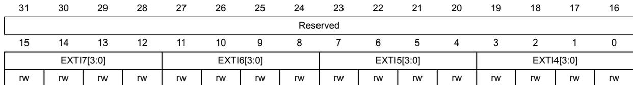
| 31 | 30 | 29 | 28 | 27 | 26 | 25 | 24 | 23 | 22 | 21 | 20 | 19 | 18 | 17 | 16 |
| Reserved | |||||||||||||||
| 15 | 14 | 13 | 12 | 11 | 10 | 9 | 8 | 7 | 6 | 5 | 4 | 3 | 2 | 1 | 0 |
| EXTI7[3:0] | EXTI6[3:0] | EXTI5[3:0] | EXTI4[3:0] | ||||||||||||
| rw | rw | rw | rw | rw | rw | rw | rw | rw | rw | rw | rw | rw | rw | rw | rw |
Bits 31:16 Reserved
Bits 15:0 EXTIx[3:0] : EXTI x configuration (x = 4 to 7)
These bits are written by software to select the source input for the EXTIx external interrupt.
0000: PA[x] pin
0001: PB[x] pin
0010: PC[x] pin
0011: PD[x] pin
0100: PE[x] pin
Other configurations are reserved
9.2.6 SYSCFG external interrupt configuration register 3 (SYSCFG_EXTICR3)
Address offset: 0x10
Reset value: 0x0000
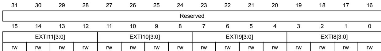
| 31 | 30 | 29 | 28 | 27 | 26 | 25 | 24 | 23 | 22 | 21 | 20 | 19 | 18 | 17 | 16 |
| Reserved | |||||||||||||||
| 15 | 14 | 13 | 12 | 11 | 10 | 9 | 8 | 7 | 6 | 5 | 4 | 3 | 2 | 1 | 0 |
| EXTI11[3:0] | EXTI10[3:0] | EXTI9[3:0] | EXTI8[3:0] | ||||||||||||
| rw | rw | rw | rw | rw | rw | rw | rw | rw | rw | rw | rw | rw | rw | rw | rw |
Bits 31:16 Reserved
Bits 15:0 EXTIx[3:0] : EXTI x configuration (x = 8 to 11)
These bits are written by software to select the source input for the EXTIx external interrupt.
0000: PA[x] pin
0001: PB[x] pin
0010: PC[x] pin
0011: PD[x] pin
0100: PE[x] pin
0101: PH[x] (only PH[1:0] and PH[10:9])
Other configurations are reserved.
9.2.7 SYSCFG external interrupt configuration register 4 (SYSCFG_EXTICR4)
Address offset: 0x14
Reset value: 0x0000
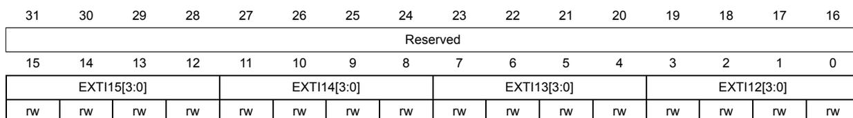
| 31 | 30 | 29 | 28 | 27 | 26 | 25 | 24 | 23 | 22 | 21 | 20 | 19 | 18 | 17 | 16 |
| Reserved | |||||||||||||||
| 15 | 14 | 13 | 12 | 11 | 10 | 9 | 8 | 7 | 6 | 5 | 4 | 3 | 2 | 1 | 0 |
| EXTI15[3:0] | EXTI14[3:0] | EXTI13[3:0] | EXTI12[3:0] | ||||||||||||
| rw | rw | rw | rw | rw | rw | rw | rw | rw | rw | rw | rw | rw | rw | rw | rw |
Bits 31:16 Reserved
Bits 15:0 EXTIx[3:0] : EXTI x configuration (x = 12 to 15)
These bits are written by software to select the source input for the EXTIx external interrupt.
0000: PA[x] pin
0001: PB[x] pin
0010: PC[x] pin
0011: PD[x] pin
0100: PE[x] pin
Other configurations are reserved.
9.2.8 SYSCFG register map
The following table gives the SYSCFG register map and the reset values.
Table 47. SYSCFG register map and reset values
| Offset | Register | 31 | 30 | 29 | 28 | 27 | 26 | 25 | 24 | 23 | 22 | 21 | 20 | 19 | 18 | 17 | 16 | 15 | 14 | 13 | 12 | 11 | 10 | 9 | 8 | 7 | 6 | 5 | 4 | 3 | 2 | 1 | 0 |
|---|---|---|---|---|---|---|---|---|---|---|---|---|---|---|---|---|---|---|---|---|---|---|---|---|---|---|---|---|---|---|---|---|---|
| 0x00 | SYSCFG_CFGR1 | Res. | Res. | Res. | Res. | Res. | Res. | Res. | Res. | Res. | Res. | Res. | Res. | Res. | Res. | Res. | Res. | Res. | Res. | Res. | Res. | Res. | Res. | BOOT_MODE | Res. | Res. | Res. | Res. | UFB | Res. | MEM_MODE | ||
| Reset value | x | x | x | x | x | ||||||||||||||||||||||||||||
| 0x04 | SYSCFG_CFGR2 | Res. | Res. | Res. | Res. | Res. | Res. | Res. | Res. | Res. | Res. | Res. | Res. | Res. | Res. | Res. | Res. | Res. | Res. | I2C3_FMP | I2C2_FMP | I2C1_FMP | I2C_PB9_FMP | I2C_PB8_FMP | I2C_PB7_FMP | I2C_PB6_FMP | Res. | Res. | Res. | Res. | Res. | Res. | FWDISEN |
| Reset value | 0 | 0 | 0 | 0 | 0 | 0 | 0 | 1 | |||||||||||||||||||||||||
| 0x08 | SYSCFG_EXTICR1 | Res. | Res. | Res. | Res. | Res. | Res. | Res. | Res. | Res. | Res. | Res. | Res. | Res. | Res. | Res. | Res. | EXTI3[3:0] | EXTI2[3:0] | EXTI1[3:0] | EXTI0[3:0] | ||||||||||||
| Reset value | 0 | 0 | 0 | 0 | 0 | 0 | 0 | 0 | 0 | 0 | 0 | 0 | 0 | 0 | 0 | 0 | |||||||||||||||||
| 0x0C | SYSCFG_EXTICR2 | Res. | Res. | Res. | Res. | Res. | Res. | Res. | Res. | Res. | Res. | Res. | Res. | Res. | Res. | Res. | Res. | EXTI7[3:0] | EXTI6[3:0] | EXTI5[3:0] | EXTI4[3:0] | ||||||||||||
| Reset value | 0 | 0 | 0 | 0 | 0 | 0 | 0 | 0 | 0 | 0 | 0 | 0 | 0 | 0 | 0 | 0 | |||||||||||||||||
Table 47. SYSCFG register map and reset values (continued)
| Offset | Register | 31 | 30 | 29 | 28 | 27 | 26 | 25 | 24 | 23 | 22 | 21 | 20 | 19 | 18 | 17 | 16 | 15 | 14 | 13 | 12 | 11 | 10 | 9 | 8 | 7 | 6 | 5 | 4 | 3 | 2 | 1 | 0 |
|---|---|---|---|---|---|---|---|---|---|---|---|---|---|---|---|---|---|---|---|---|---|---|---|---|---|---|---|---|---|---|---|---|---|
| 0x10 | SYSCFG_EXTICR3 | Res. | Res. | Res. | Res. | Res. | Res. | Res. | Res. | Res. | Res. | Res. | Res. | Res. | Res. | Res. | Res. | EXTI11[3:0] | EXTI10[3:0] | EXTI9[3:0] | EXTI8[3:0] | ||||||||||||
| Reset value | 0 | 0 | 0 | 0 | 0 | 0 | 0 | 0 | 0 | 0 | 0 | 0 | 0 | 0 | 0 | ||||||||||||||||||
| 0x14 | SYSCFG_EXTICR4 | Res. | Res. | Res. | Res. | Res. | Res. | Res. | Res. | Res. | Res. | Res. | Res. | Res. | Res. | Res. | Res. | EXTI15[3:0] | EXTI14[3:0] | EXTI13[3:0] | EXTI12[3:0] | ||||||||||||
| Reset value | 0 | 0 | 0 | 0 | 0 | 0 | 0 | 0 | 0 | 0 | 0 | 0 | 0 | 0 | 0 | ||||||||||||||||||
| 0x18 | COMP1_CTRL | Refer to Section 14: Comparator (COMP) | |||||||||||||||||||||||||||||||
| 0x1C | COMP2_CTRL | ||||||||||||||||||||||||||||||||
| 0x20 | SYSCFG_CFGR3 | REF_LOCK | VREFINT_RDYF | Res. | Res. | Res. | Res. | Res. | Res. | Res. | Res. | Res. | Res. | Res. | Res. | Res. | Res. | Res. | Res. | Res. | ENBUF_VREFINT_COMP2 | Res. | Res. | ENBUF_SENSOR_ADC | ENBUF_VREFINT_ADC | Res. | Res. | SEL_VREF_OUT | Res. | Res. | Res. | EN_VREFINT | |
| Reset value | 0 | 0 | 0 | 0 | 0 | 0 | 0 | 0 | 0 | ||||||||||||||||||||||||
Refer to Section 2.2 on page 51 for the register boundary addresses.