7. Reset and clock control (RCC)
7.1 Reset
There are three types of reset, defined as system reset, power reset and RTC domain reset.
7.1.1 System reset
A system reset sets all registers to their reset values unless specified otherwise in the register description.
A system reset is generated when one of the following events occurs:
- • A low level on the NRST pin (external reset)
- • Window watchdog end-of-count condition (WWDG reset)
- • Independent watchdog end-of-count condition (IWDG reset)
- • A software reset (SW reset) (see Software reset )
- • Low-power management reset (see Low-power management reset )
- • Option byte loader reset (see Option byte loader reset )
- • Exit from Standby mode
- • Firewall protection (see Section 5: Firewall (FW) )
The reset source can be identified by checking the reset flags in the control/status register, RCC_CSR (see Section 7.3.20 ).
Software reset
The SYSRESETREQ bit in Cortex ® -M0+ AIRCR register (Application Interrupt and Reset Control Register) must be set to force a software reset on the device. Refer to Arm ® Cortex ® -M0+ Technical Reference Manual for more details.
Low-power management reset
There are two ways to generate a low-power management reset:
- • Reset generated when entering Standby mode:
This type of reset is enabled by resetting nRST_STDBY bit in user option bytes. In this case, whenever a Standby mode entry sequence is successfully executed, the device is reset instead of entering Standby mode. - • Reset when entering Stop mode:
This type of reset is enabled by resetting nRST_STOP bit in user option bytes. In this case, whenever a Stop mode entry sequence is successfully executed, the device is reset instead of entering Stop mode.
Option byte loader reset
The Option byte loader reset is generated when the OBL_LAUNCH bit (bit 18) is set in the FLASH_PECR register. This bit is used to launch by software the option byte loading.
For further information on the user option bytes, refer to Section 3: Flash program memory and data EEPROM (FLASH) .
7.1.2 Power reset
A power reset is generated when one of the following events occurs:
- • Power-on/power-down reset (POR/PDR reset)
- • BOR reset
A power reset sets all registers to their reset values including for the RTC domain (see Figure 16 )
These sources act on the NRST pin and it is always kept low during the delay phase. The RESET service routine vector is fixed at address 0x0000_0004 in the memory map. For more details, refer to Table 53: List of vectors .
The system reset signal provided to the device is output on the NRST pin (except the Exit from Standby reset which is not output on the NRST pin but generates system reset).
The pulse generator guarantees a minimum reset pulse duration of 20 µs for each internal reset source. In case of an external reset, the reset pulse is generated while the NRST pin is asserted low.
When an internal reset occurs, the internal pull-up resistor (RPU) is deactivated in order to save the power consumption through the pull-up resistor.
Figure 16. Simplified diagram of the reset circuit
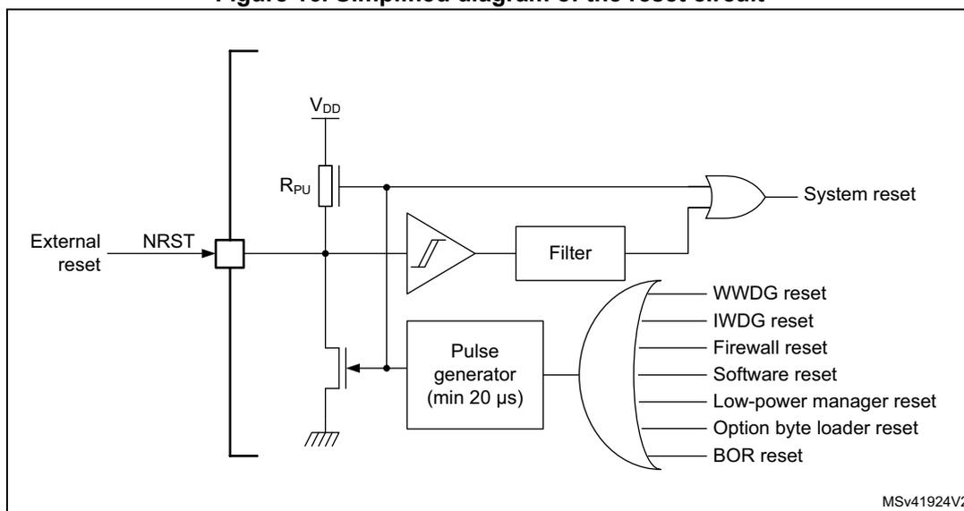
The diagram illustrates the internal reset circuitry. An external reset signal enters the NRST pin. A pull-up resistor (R PU ) connected to V DD pulls the NRST line high when no external reset is present. A transistor is used to deactivate this pull-up resistor during internal reset events. The NRST line is connected to an inverter, which drives a filter. The output of the filter is connected to one input of an OR gate, which produces the 'System reset' signal. Another input to this OR gate comes from a 'Pulse generator (min 20 µs)'. This pulse generator is triggered by various internal reset sources: WWDOG reset, IWDG reset, Firewall reset, Software reset, Low-power manager reset, Option byte loader reset, and BOR reset. The diagram is labeled with 'MSV41924V2' in the bottom right corner.
7.1.3 RTC and backup registers reset
The RTC peripheral, RTC clock source selection (in RCC_CSR) and the backup registers are reset only when one of the following events occurs:
- • A software reset, triggered by setting the RTCRST bit in the RCC_CSR register (see Section 7.3.20 )
- • Power reset (BOR/POR/PDR).
7.2 Clocks
Four different clock sources can be used to drive the system clock (SYSCLK):
- • HSI16 (high-speed internal) oscillator clock
- • HSE (high-speed external) oscillator clock
The HSE external quartz connexion is available only on cat. 2 devices in LQFP48 package.
- • PLL clock
- • MSI (multispeed internal) oscillator clock
The MSI at 2.1MHz is used as system clock source after startup from power reset, system or RTC domain reset, and after wake-up from Standby mode.
The HSI16, HSI16 divided by 4, or the MSI at any of its possible frequency can be used to wake up from Stop mode.
The devices have two secondary clock sources:
- • 37 kHz low speed internal RC (LSI RC) which drives the independent watchdog and optionally the RTC used for Auto-wakeup from Stop/Standby mode and the LPTIMER.
- • 32.768 kHz low speed external crystal (LSE crystal) which optionally drives the real-time clock (RTCCLK), the LPTIMER and USARTs.
Each clock source can be switched on or off independently when it is not used to optimize power consumption.
Several prescalers can be used to configure the AHB frequency and the two APBs (APB1 and APB2) domains. The maximum frequency of AHB, APB1 and the APB2 domains is 32 MHz. It depends on the device voltage range. For more details refer to Section 6.1.4: Dynamic voltage scaling management .
All the peripheral clocks are derived from the system clock (SYSCLK) except:
- • The ADC can be derived either from the APB clock or the HSI16 clock.
- • The LPUART1 and USART1/2 clock which is derived (selected by software) from one of the four following sources:
- – system clock
- – HSI16 clock
- – LSE clock
- – APB clock (PCLK)
- • The I2C1 clock which is derived (selected by software) from one of the three following sources:
- – system clock
- – HSI16 clock
- – APB clock (PCLK)
- • The LPTIMER clock which is derived (selected by software) from one of the four following sources:
- – HSI16 clock
- – LSE clock
- – LSI clock
- – APB clock (PCLK)
- • The RTC clock which is derived from the following clock sources:
- – LSE clock,
- – LSI clock,
- – 4 MHz HSE_RTC (HSE divided by a programmable prescaler).
- • IWDG clock which is always the LSI clock.
The system clock (SYSCLK) frequency must be higher or equal to the RTC clock frequency.
The RCC feeds the Cortex ® System Timer (SysTick) external clock with the AHB clock (HCLK) divided by 8. The SysTick can work either with this clock or with the Cortex ® clock (HCLK), configurable in the SysTick Control and Status Register.
Figure 17. Clock tree
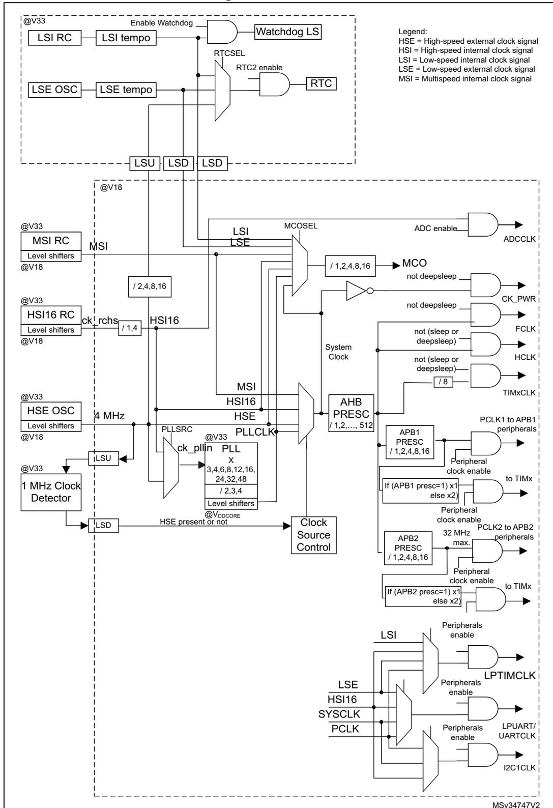
The diagram illustrates the internal clock tree of the microcontroller. It shows how various clock sources are selected and distributed to different parts of the system. Key components include:
- Watchdog and RTC: LSI RC and LSE OSC provide low-speed internal and external clock signals respectively, processed through tempo blocks and multiplexers to drive the Watchdog LS and RTC.
- Main System Clock: Multiple sources (MSI RC, HSI16 RC, HSE OSC, 1 MHz Clock Detector) are selected via a multiplexer. The HSE path includes a PLL block with programmable dividers and multipliers. The selected source is divided by AHB PRESC (/1, 2, ..., 512) to provide the main system clock.
- Peripheral Clocks:
The system clock is further divided and multiplexed to drive various peripherals:
- ADCCLK: Derived from the system clock via a /1, 2, 4, 8, 16 divider.
- CK_PWR, FCLK, HCLK: Derived from the system clock, with some paths including 'not deepsleep' or 'not (sleep or deepsleep)' logic gates.
- TIMxCLK: Derived from the system clock via a /8 divider.
- PCLK1 and PCLK2: Derived from the system clock through APB1 and APB2 prescalers (/1, 2, 4, 8, 16) and additional multiplexers, with logic for 'if (APB1 presc=1) x1 else x2'.
- LPTIMCLK, LPUART/UARTCLK, I2C1CLK: Low-power peripheral clocks derived from LSI, LSE, HSI16, SYSCLK, or PCLK sources through individual multiplexers and enable logic.
- MCO (Microcontroller Clock Output): A programmable output clock derived from various internal sources (LSI, LSE, MSI, HSI16, HSE, PLLCLK) via a /1, 2, 4, 8, 16 divider.
Legend:
HSE = High-speed external clock signal
HSI = High-speed internal clock signal
LSI = Low-speed internal clock signal
LSE = Low-speed external clock signal
MSI = Multispeed internal clock signal
MSv34747V2
- 1. For full details about the internal and external clock source characteristics, please refer to the “Electrical characteristics” section in your device datasheet.
The timer clock frequencies are automatically fixed by hardware. There are two cases:
- 1. If the APB prescaler is 1, the timer clock frequencies are set to the same frequency as that of the APB domain to which the timers are connected.
- 2. Otherwise, they are set to twice ( \( \times 2 \) ) the frequency of the APB domain to which the timers are connected.
\( f_{CLK} \) acts as Cortex ® -M0+ free running clock. For more details refer to the Section 27: Debug support (DBG) .
7.2.1 HSE clock
The high speed external clock signal (HSE) can be generated from two possible clock sources:
- • HSE external crystal/ceramic resonator
- • HSE user external clock
The resonator and the load capacitors have to be placed as close as possible to the oscillator pins in order to minimize output distortion and startup stabilization time. The loading capacitance values must be adjusted according to the selected oscillator.
Table 42. HSE/LSE clock sources
| Clock source | Hardware configuration |
|---|---|
| External clock for category 2 (LQFP48 only), category 3 and 5 devices | 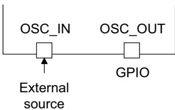 MSv31915V1 |
| Clock source | Hardware configuration |
|---|---|
| External clock for category 1 and 2 devices (packages with less than 48 pins) | 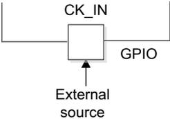 MSv36151V1 |
| Crystal/Ceramic resonators for category 2 (LQFP48 only), category 3 and 5 devices | 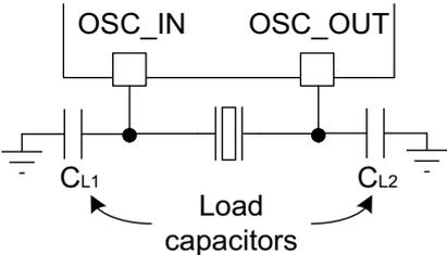 MSv31916V1 |
External source (HSE bypass)
In this mode, an external clock source must be provided. It can have a frequency of up to 32 MHz. This mode is selected by setting the HSEBYP and HSEON bits in the RCC_CR register ( see Section 7.3.1: Clock control register (RCC_CR) ). The external clock signal with ~50% duty cycle has to drive the following pin ( see Figure 42 ):
- • On devices where OSC_IN and OSC_OUT pins are available: the OSC_IN pin must be driven while the OSC_OUT pin should be left hi-Z.
- • Otherwise, the CK_IN pin must be driven.
Note: For details on pin availability, refers to the pinout section in your device datasheet.
The external clock signal can be square, sinus or triangle. To minimize the consumption, it is recommended to use the square signal.
External crystal/ceramic resonator (HSE crystal)
The 1 to 24 MHz external oscillator has the advantage of producing a very accurate rate on the main clock.
The associated hardware configuration is shown in Figure 42 . Refer to the electrical characteristics section of the datasheet for more details.
The HSERDY flag of the RCC_CR register ( see Section 7.3.1 ) indicates whether the HSE oscillator is stable or not. At startup, the HSE clock is not released until this bit is set by hardware. An interrupt can be generated if enabled in the RCC_CR register .
The HSE Crystal can be switched on and off using the HSEON bit in the RCC_CR register .
For code example, refer to A.4.1: HSE start sequence code example .
7.2.2 HSI16 clock
The HSI16 clock signal is generated from an internal 16 MHz RC oscillator. It can be used directly as a system clock or as PLL input.
The HSI16 clock can be used after wake-up from the Stop low-power mode, this ensures a smaller wake-up time than a wake-up using MSI clock.
The HSI16 RC oscillator has the advantage of providing a clock source at low cost (no external components). It also has a faster startup time than the HSE crystal oscillator however, even with calibration the frequency is less accurate than an external crystal oscillator or ceramic resonator.
The HSI16 clock can be kept running in Stop mode by setting HSI16KERON bit in RCC_CR register (see Section 7.3.1: Clock control register (RCC_CR) ). In this case the HSI16 clock can be used for dedicated peripherals which can run in Stop mode.
Calibration
RC oscillator frequencies can vary from one chip to another due to manufacturing process variations, this is why each device is factory calibrated by ST for 1% accuracy at an ambient temperature, \( T_A \) , of 25 °C.
After reset, the factory calibration value is loaded in the HSI16CAL[7:0] bits in the Internal Clock Sources Calibration Register (RCC_ICSCR) (see Section 7.3.2 ).
If the application is subject to voltage or temperature variations, this may affect the RC oscillator speed. You can trim the HSI16 frequency in the application by using the HSI16TRIM[4:0] bits in the RCC_ICSCR register. For more details on how to measure the HSI16 frequency variation please refer to Section 7.2.14: Internal/external clock measurement using TIM21 .
The HSI16RDY flag in the RCC_CR register indicates whether the HSI16 oscillator is stable or not. At startup, the HSI16 RC output clock is not released until this bit is set by hardware.
The HSI16 RC oscillator can be switched on and off using the HSI16ON bit in the RCC_CR register.
7.2.3 MSI clock
The MSI clock signal is generated from an internal RC oscillator. Its frequency range can be adjusted by software by using the MSIRANGE[2:0] bits in the RCC_ICSCR register (see Section 7.3.2: Internal clock sources calibration register (RCC_ICSCR) ). Seven frequency ranges are available: 65.536 kHz, 131.072 kHz, 262.144 kHz, 524.288 kHz, 1.048 MHz, 2.097 MHz (default value) and 4.194 MHz.
The MSI clock is always used as system clock after restart from Reset and wake-up from Standby. After wake-up from Stop mode, the MSI clock can be selected as system clock instead of HSI16 (or HSI16/4).
When the device restarts after a reset or a wake-up from Standby, the MSI frequency is set to its default value. The MSI frequency does not change after waking up from Stop.
The MSI RC oscillator has the advantage of providing a low-cost (no external components) low-power clock source. It is used as wake-up clock in low-power modes to reduce power consumption.
The MSIRDY flag in the RCC_CR register indicates whether the MSI RC is stable or not. At startup, the MSI RC output clock is not released until this bit is set by hardware.
The MSI RC can be switched on and off by using the MSION bit in the RCC_CR register (see Section 7.3.1 ).
It can also be used as a backup clock source (auxiliary clock) if the HSE crystal oscillator fails. Refer to Section 7.2.9: HSE clock security system (CSS) on page 177 .
Calibration
The MSI RC oscillator frequency can vary from one chip to another due to manufacturing process variations, this is why each device is factory calibrated by ST for 1% accuracy at an ambient temperature, \( T_A \) , of 25 °C.
After reset, the factory calibration value is loaded in the MSICAL[7:0] bits in the RCC_ICSCR register. If the application is subject to voltage or temperature variations, this may affect the RC oscillator speed. You can trim the MSI frequency in the application by using the MSITRIM[7:0] bits in the RCC_ICSCR register. For more details on how to measure the MSI frequency variation please refer to Section 7.2.14: Internal/external clock measurement using TIM21 .
7.2.4 PLL
The internal PLL can be clocked by the HSI16 RC or HSE clocks.
The PLL input clock frequency must range between 2 and 24 MHz.
The desired frequency is obtained by using the multiplication factor and output division embedded in the PLL:
- • The system clock is derived from the PLL VCO divided by the output division factor.
Note: The application software must set correctly the PLL multiplication factor to avoid exceeding 96 MHz as PLLVCO when the product is in range 1, 48 MHz as PLLVCO when the product is in range 2, 24 MHz when the product is in range 3.
It must also set correctly the output division to avoid exceeding 32 MHz as SYSCLK.
The minimum input clock frequency for PLL is 2 MHz (when using HSE as PLL source).
The PLL configuration (selection of the source clock, multiplication factor and output division factor) must be performed before enabling the PLL. Once the PLL is enabled, these parameters cannot be changed.
To modify the PLL configuration, proceed as follows:
- 1. Disable the PLL by setting PLLON to 0.
- 2. Wait until PLLRDY is cleared. The PLL is now fully stopped.
- 3. Change the desired parameter.
- 4. Enable the PLL again by setting PLLON to 1.
An interrupt can be generated when the PLL is ready if enabled in the RCC_CIER register (see Section 7.3.4 ).
For code example, refer to A.4.2: PLL configuration modification code example .
7.2.5 LSE clock
The LSE crystal is a 32.768 kHz low speed external crystal or ceramic resonator. It has the advantage of providing a low-power but highly accurate clock source to the real-time clock peripheral (RTC) for clock/calendar or other timing functions.
The LSE crystal is switched on and off through the LSEON bit in the RCC_CSR register (see Section 7.3.20 ).
The crystal oscillator driving strength can be changed at runtime through the LSEDRV[1:0] bits of the RCC_CSR register to obtain the best compromise between robustness and short start-up time on one hand and low power consumption on the other hand. The driving capability should be changed dynamically to determine the driving level that best matches the used crystal. In the final application, it is then recommended to program this value in LSEDRV[1:0] bits.
The LSERDY flag in the RCC_CSR register indicates whether the LSE crystal is stable or not. At startup, the LSE crystal output clock signal is not released until this bit is set by hardware. An interrupt can be generated if enabled in the RCC_CIER register (see Section 7.3.4 ).
External source (LSE bypass)
In this mode, an external clock source must be provided. It can have a frequency of up to 1 MHz. This mode is selected by setting the LSEBYP and LSEON bits in the RCC_CSR (see Section 7.3.1 ). The external clock signal (square, sinus or triangle) with ~50% duty cycle has to drive the OSC32_IN pin while the OSC32_OUT pin should be left Hi-Z (see Figure 42 ).
7.2.6 LSI clock
The LSI RC acts as an low-power clock source that can be kept running in Stop and Standby mode for the independent watchdog (IWDG). The clock frequency is around 37 kHz.
The LSI RC oscillator can be switched on and off using the LSION bit in the RCC_CSR register (see Section 7.3.20 ).
The LSIRDY flag in RCC_CSR indicates whether the low-speed internal oscillator is stable or not. At startup, the clock is not released until this bit is set by hardware. An interrupt can be generated if enabled in the RCC_CIER (see Section 7.3.4 ).
Since the IWDG is activated, the LSI oscillator cannot be stopped by LSION=0. The LSI oscillator is stopped by system reset (except if IWDG is enabled by hardware option through WDG_SW option bit in FLASH_OPTER register). If the IWDG was enabled by software, then the LSI oscillator must be enabled again after system reset to ensure correct IWDG and/or RTC operation.
LSI measurement
The frequency dispersion of the LSI oscillator can be measured to have accurate RTC time base and/or IWDG timeout (when LSI is used as clock source for these peripherals) with an acceptable accuracy. For more details, refer to the electrical characteristics section of the datasheets. For more details on how to measure the LSI frequency, please refer to Section 7.2.14: Internal/external clock measurement using TIM21 .
7.2.7 System clock (SYSCLK) selection
Four different clock sources can be used to drive the system clock (SYSCLK):
- • The HSI16 oscillator
- • The HSE oscillator
- • The PLL
- • The MSI oscillator clock (default after reset)
When a clock source is used directly or through the PLL as system clock, it is not possible to stop it.
A switch from one clock source to another occurs only if the target clock source is ready (clock stable after startup delay or PLL locked). If a clock source which is not yet ready is selected, the switch will occur when the clock source will be ready. Status bits in the RCC_CR register indicate which clock(s) is (are) ready and which clock is currently used as system clock.
7.2.8 System clock source frequency versus voltage range
The following table gives the different clock source maximum frequencies depending on the product voltage range.
Table 43. System clock source frequency
| Product voltage range | Clock frequency | |||
|---|---|---|---|---|
| MSI | HSI16 | HSE | PLL | |
| Range 1 (1.8 V) | 4.2 MHz | 16 MHz | HSE 32 MHz (external clock) or 24 MHz (crystal) | 32 MHz (PLLVC0 max = 96 MHz) |
| Range 2 (1.5 V) | 4.2 MHz | 16 MHz | 16 MHz | 16 MHz (PLLVC0 max = 48 MHz) |
| Range 3 (1.2 V) | 4.2 MHz | NA | 8 MHz | 4 MHz (PLLVC0 max = 24 MHz) |
7.2.9 HSE clock security system (CSS)
The Clock security system can be activated on the HSE by software. In this case, the clock detector is enabled after the HSE oscillator startup delay, and disabled when this oscillator is stopped.
If an HSE clock failure is detected, this oscillator is automatically disabled and an CSSHSEI interrupt (Clock Security System Interrupt) is generated to inform the software of the failure, thus allowing the MCU to perform rescue operations. The CSSHSEI is linked to the Cortex ® -M0+ NMI (Non-Maskable Interrupt) exception vector.
Note: Once the CSSHSE is enabled, if the HSE clock fails, the CSSHSE interrupt occurs and an NMI is automatically generated. The NMI is executed indefinitely unless the CSSHSE interrupt pending bit is cleared. As a consequence, the NMI interrupt service routine (ISR) must clear the CSSHSE interrupt by setting the CSSHSEC bit in the RCC_CICR register.
If the HSE oscillator is used directly or indirectly as the system clock (indirectly means: it is used as PLL input clock, and the PLL clock is used as system clock), a detected failure causes a switch of the system clock and the disabling of the HSE oscillator. If the HSE oscillator clock is the clock entry of the PLL used as system clock when the failure occurs, the PLL is disabled too.
When an HSE failure occurs, the system clock can be switched to the MSI or to the internal 16-MHz HSI clock depending on the value of STOPWUCK bit in the RCC_CFGR register.
Note: Category 1 devices do not feature HSE clock security system. The HSE clock is available only in bypass mode.
7.2.10 LSE Clock Security System
Clock Security System can be activated on the LSE by software. This is done by writing the CSSLSEON bit in the RCC_CSR register. This bit can be disabled by a hardware reset, an RTC software reset, or after an LSE clock failure detection. CSSLSEON bit must be written after the LSE and LSI clocks are enabled (LSEON and LSION set) and ready (LSERDY and LSIRDY bits set by hardware), and after the RTC clock has been selected through the RTCSEL bit.
The LSE CSS works in all modes: run, Sleep, Stop and Standby.
If a failure is detected on the external 32 kHz oscillator, the LSE clock is no longer supplied to the RTC but the content of the registers does not change.
A wakeup is generated in Standby mode. In any other modes, an interrupt can be sent to wake-up the software (see Section 7.3.4 ).
The software MUST then reset the CSSLSEON bit and stop the defective 32 kHz oscillator by resetting LSEON bit. It can change the RTC clock source (LSI, HSE or no clock) through the RTCSEL bit, or take any required action to secure the application.
The frequency of LSE oscillator must be higher than 30 kHz to avoid false positive CSS detection.
7.2.11 RTC clock
The RTC has the same clock source which can be either the LSE, the LSI, or the HSE 4 MHz clock (HSE divided by a programmable prescaler). It is selected by programming the RTCSEL[1:0] bits in the RCC_CSR register (see Section 7.3.20 ) and the RTCPRE[1:0] bits in the RCC_CR register (see Section 7.3.1 ).
Once the RTC clock source have been selected, the only possible way of modifying the selection is to set the RTCRST bit in the RCC_CSR register, or by a POR.
If the LSE or LSI is used as RTC clock source, the RTC continues to work in Stop and Standby low-power modes, and can be used as wakeup source. However, when the HSE is the RTC clock source, the RTC cannot be used in the Stop and Standby low-power modes.
When the RTC is clocked by the LSE, the RTC remains clocked and functional under system reset.
Note: To be able to read the RTC calendar register when the APB1 clock frequency is less than seven times the RTC clock frequency ( \( 7 \times \text{RTCLCK} \) ), the software must read the calendar time and date registers twice.
If the second read of the RTC_TR gives the same result as the first read, this ensures that the data is correct. Otherwise a third read access must be done.
7.2.12 Watchdog clock
If the Independent watchdog (IWDG) is started by either hardware option or software access, the LSI oscillator is forced ON and cannot be disabled. After the LSI oscillator temporization, the clock is provided to the IWDG.
If the IWDG was enabled by software, the LSI clock is disabled after system reset. The LSI oscillator must then be enabled again to ensure correct IWDG operation.
7.2.13 Clock-out capability
The microcontroller clock output (MCO) capability allows the clock to be output onto the external MCO pin using a configurable prescaler (1, 2, 4, 8, or 16). The configuration registers of the corresponding GPIO port must be programmed in alternate function mode. One of 7 clock signals can be selected as the MCO clock:
- • SYSCLK
- • HSI16
- • MSI
- • HSE
- • PLL
- • LSI
- • LSE
The selection is controlled by the MCOSEL[3:0] bits of the RCC_CFGR register (see Section 7.3.19 ).
For code example, refer to A.4.3: MCO selection code example .
7.2.14 Internal/external clock measurement using TIM21
It is possible to indirectly measure the frequency of all on-board clock source generators by means of the TIM21 channel 1 input capture, as represented on Figure 18 .
Figure 18. Using TIM21 channel 1 input capture to measure frequencies
![Figure 18: Using TIM21 channel 1 input capture to measure frequencies. The diagram shows a TIM21 block with three input pins: TI(1), ETR, and TI(2). TI(1) is connected to a multiplexer output labeled TI1_RMP[2:0]. The multiplexer has seven inputs: MSI, LSI, HSE_RTC, LSE, and two GPIO pins. ETR is connected to a GPIO pin. TI(2) is connected to the LSE input. The diagram is labeled MS32913V1.](/RM0377-STM32L0x1/5aa18c874a16d82357f315358d51b5e1_img.jpg)
TIM21 has an input multiplexer that selects which of the I/O or the internal clock is to trigger the input capture. This selection is performed through the TI1_RMP [2:0] bits in the TIM21_OR register.
The primary purpose of connecting the LSE to the channel 1 input capture is to be able to accurately measure the HSI16 and MSI system clocks (for this, either the HSI16 or MSI should be used as the system clock source). The number of HSI16 (MSI, respectively) clock counts between consecutive edges of the LSE signal provides a measure of the internal clock period. Taking advantage of the high precision of LSE crystals (typically a few tens of ppm's), it is possible to determine the internal clock frequency with the same resolution, and trim the source to compensate for manufacturing-process- and/or temperature- and voltage-related frequency deviations.
The MSI and HSI16 oscillators both have dedicated user-accessible calibration bits for this purpose.
The basic concept consists in providing a relative measurement (e.g. the HSI16/LSE ratio): the precision is therefore closely related to the ratio between the two clock sources. The higher the ratio, the better the measurement.
It is however not possible to have a good enough resolution when the MSI clock is low (typically below 1 MHz). In this case, it is advised to:
- • accumulate the results of several captures in a row
- • use the timer's input capture prescaler (up to 1 capture every 8 periods)
- • use the RTC_OUT signal at 512 Hz (when the RTC is clocked by the LSE) as the input for the channel1 input capture. This improves the measurement precision
TIM21 can also be used to measure the LSI, MSI, or HSE_RTC: this is useful for applications with no crystal. The ultra-low-power LSI oscillator has a wide manufacturing process deviation: by measuring it as a function of the HSI16 clock source, its frequency can be determined with the precision of the HSI16. The HSE_RTC frequency (HSE divided by a programmable prescaler) being relatively high (4 MHz), the relative frequency measurement is not very accurate. Its main purpose is consequently to obtain a rough indication of the external crystal frequency. This can be useful to meet the requirements of the IEC 60730/IEC 61335 standards, which require to be able to determine harmonic or subharmonic frequencies (–50/+100% deviations).
7.2.15 Clock-independent system clock sources for TIM2/TIM21/TIM22
In a number of applications using the 32.768 kHz clock as RTC timebase, timebases completely independently from the system clock are useful. This allows to schedule tasks without having to take into account the processor state (the processor may be stopped or executing at low, medium or full speed).
For this purpose, the LSE clock is internally redirected to the 3 timers' ETR inputs, which are used as additional clock sources. This gives up to three independent time bases (using the auto-reload feature) with 1 or 2 compare additional channels for fractional events. For instance, the TIM21 auto-reload interrupt can be programmed for a 1 second tick interrupt with an additional interrupt occurring 250 ms after the main tick.
Note: In this configuration, make sure that you have at least a ratio of 2 between the external clock (LSE) and the APB clock. If the application uses an APB clock frequency lower than twice the LSE clock frequency (typically LSE = 32.768 kHz, so twice LSE = 65.536 kHz), it is mandatory to use the external trigger prescaler feature of the timer: it can divide the ETR clock by up to 8.
7.3 RCC registers
Refer to Section 1.2 for a list of abbreviations used in register descriptions.
7.3.1 Clock control register (RCC_CR)
Address offset: 0x00
System Reset value: 0b0000 0000 00XX 0X00 0000 0011 0000 0000 where X is undefined
Power-on reset value: 0x0000 0300
Access: no wait state, word, half-word and byte access
| 31 | 30 | 29 | 28 | 27 | 26 | 25 | 24 | 23 | 22 | 21 | 20 | 19 | 18 | 17 | 16 |
|---|---|---|---|---|---|---|---|---|---|---|---|---|---|---|---|
| Res. | Res. | Res. | Res. | Res. | Res. | PLL RDY | PLLON | Res. | Res. | RTCPRE[1:0] | CSSHSEON | HSE BYP | HSE RDY | HSE ON | |
| r | rw | rw | rw | rw | rw | r | rw | ||||||||
| 15 | 14 | 13 | 12 | 11 | 10 | 9 | 8 | 7 | 6 | 5 | 4 | 3 | 2 | 1 | 0 |
|---|---|---|---|---|---|---|---|---|---|---|---|---|---|---|---|
| Res. | Res. | Res. | Res. | Res. | Res. | MSI RDY | MSION | Res. | Res. | HSI16 OUTEN | HSI16 DIVF | HSI16 DIVEN | HSI16 RDYF | HSI16K ERON | HSI16 ON |
| r | rw | rw | r | rw | r | rw | rw |
Bits 31:26 Reserved, must be kept at reset value.
Bit 25 PLLRDY : PLL clock ready flag
This bit is set by hardware to indicate that the PLL is locked.
0: PLL unlocked
1: PLL locked
Bit 24 PLLON : PLL enable bit
This bit is set and cleared by software to enable PLL.
Cleared by hardware when entering Stop or Standby mode. This bit can not be reset if the PLL clock is used as system clock or is selected to become the system clock.
0: PLL OFF
1: PLL ON
Bits 23:22 Reserved, must be kept at reset value.
Bits 21:20 RTCPRE[1:0] RTC prescaler
These bits are set and reset by software to obtain a 4 MHz clock from HSE. This prescaler cannot be modified if HSE is enabled (HSEON = 1). These bits are reset by a power-on reset. Their value is not modified by a system reset.
00: HSE is divided by 2 for RTC clock
01: HSE is divided by 4 for RTC clock
10: HSE is divided by 8 for RTC clock
11: HSE is divided by 16 for RTC clock
Bit 19 CSSHSEON : Clock security system on HSE enable bit
This bit is set by software to enable the clock security system (CSS) on HSE. This bit is "set only" (disabled by system reset). When CSSHSEON is set, the clock detector is enabled by hardware when the HSE oscillator is ready, and disabled by hardware if an oscillator failure is detected.
0: Clock security system OFF (clock detector OFF)
1: Clock security system ON (clock detector ON if HSE oscillator is stable, OFF otherwise)
Bit 18 HSEBYP: HSE clock bypass bitThis bit is set and cleared by software to bypass the oscillator with an external clock. The external clock must be enabled with the HSEON bit, to be used by the device.
The HSEBYP bit can be written only if the HSE oscillator is disabled. This bit is reset by power-on reset. Its value is not modified by system reset
0: HSE oscillator not bypassed
1: HSE oscillator bypassed with an external clock
Bit 17 HSERDY: HSE clock ready flagThis bit is set by hardware to indicate that the HSE oscillator is stable. After the HSEON bit is cleared, HSERDY goes low after 6 HSE oscillator clock cycles.
0: HSE oscillator not ready
1: HSE oscillator ready
Bit 16 HSEON: HSE clock enable bitThis bit is set and cleared by software.
Cleared by hardware to stop the HSE oscillator when entering Stop or Standby mode. This bit cannot be reset if the HSE oscillator is used directly or indirectly as the system clock.
0: HSE oscillator OFF
1: HSE oscillator ON
Bits 15:10 Reserved, must be kept at reset value.
Bit 9 MSIRDY: MSI clock ready flagThis bit is set by hardware to indicate that the MSI oscillator is stable.
0: MSI oscillator not ready
1: MSI oscillator ready
Note: Once the MSION bit is cleared, MSIRDY goes low after 6 MSI clock cycles.
Bit 8 MSION: MSI clock enable bitThis bit is set and cleared by software.
Set by hardware to force the MSI oscillator ON when exiting from Stop or Standby mode, or in case of a failure of the HSE oscillator used directly or indirectly as system clock. This bit cannot be cleared if the MSI is used as system clock.
0: MSI oscillator OFF
1: MSI oscillator ON
Bits 7:6 Reserved, must be kept at reset value.
Bit 5 HSI16OUTEN: 16 MHz high-speed internal clock output enableThis bit is set and cleared by software. When this bit is set, TIM2 ETR input is connected to the 16 MHz HSI output clock (HSI16) provided ETR_RMP is set to 011 in TIM2 option register (TIM2_OR) . This bit can be written anytime by the application.
0: HSI16 output clock disabled
1: HSI16 output clock enabled
Bit 4 HSI16DIVF: HSI16 divider flagThis bit is set and reset by hardware. As a write in HSI16DIVEN has not an immediate effect on the frequency, this flag indicates the current status of the HSI16 divider.
0: 16 MHz HSI clock not divided
1: 16 MHz HSI clock divided by 4
Bit 3 HSI16DIVEN: HSI16 divider enable bitThis bit is set and reset by software to enable/disable the 16 MHz HSI divider by 4. It can be written anytime.
0: no 16 MHz HSI division requested
1: 16 MHz HSI division by 4 requested
Bit 2 HSI16RDYF: Internal high-speed clock ready flagThis bit is set by hardware to indicate that the HSI 16 MHz oscillator is stable. After the HSI16ON bit is cleared, HSI16RDY goes low after 6 HSI16 clock cycles.
0: HSI 16 MHz oscillator not ready
1: HSI 16 MHz oscillator ready
Bit 1 HSI16KERON: High-speed internal clock enable bit for some IP kernelsThis bit is set and reset by software to force the HSI 16 MHz oscillator ON, even in Stop mode, so that it can be quickly available as kernel clock for USARTs or I2C1. This bit has no effect on the value of HSI16ON.
0: HSI 16 MHz oscillator not forced ON
1: HSI 16 MHz oscillator forced ON even in Stop mode
Bit 0 HSI16ON: 16 MHz high-speed internal clock enableThis bit is set and cleared by software. It cannot be cleared if the 16 MHz HSI is used directly or indirectly as system clock.
0: HSI16 oscillator OFF
1: HSI16 oscillator ON
7.3.2 Internal clock sources calibration register (RCC_ICSCR)
Address offset: 0x04
Reset value: 0x00XX B0XX where X is undefined.
Access: no wait state, word, half-word and byte access
| 31 | 30 | 29 | 28 | 27 | 26 | 25 | 24 | 23 | 22 | 21 | 20 | 19 | 18 | 17 | 16 |
|---|---|---|---|---|---|---|---|---|---|---|---|---|---|---|---|
| MSITRIM[7:0] | MSICAL[7:0] | ||||||||||||||
| rw | rw | rw | rw | rw | rw | rw | rw | r | r | r | r | r | r | r | r |
| 15 | 14 | 13 | 12 | 11 | 10 | 9 | 8 | 7 | 6 | 5 | 4 | 3 | 2 | 1 | 0 |
| MSIRANGE[2:0] | HSI16TRIM[4:0] | HSI16CAL[7:0] | |||||||||||||
| rw | rw | rw | rw | rw | rw | rw | rw | r | r | r | r | r | r | r | r |
Bits 31:24 MSITRIM[7:0] : MSI clock trimming
These bits are set by software to adjust MSI calibration.
These bits provide an additional user-programmable trimming value that is added to the MSICAL[7:0] bits. They can be programmed to compensate for the variations in voltage and temperature that influence the frequency of the internal MSI RC.
Bits 23:16 MSICAL[7:0] : MSI clock calibration
These bits are automatically initialized at startup.
Bits 15:13 MSIRANGE[2:0] : MSI clock ranges
These bits are set by software to choose the frequency range of MSI. 7 frequency ranges are available:
- 000: range 0 around 65.536 kHz
- 001: range 1 around 131.072 kHz
- 010: range 2 around 262.144 kHz
- 011: range 3 around 524.288 kHz
- 100: range 4 around 1.048 MHz
- 101: range 5 around 2.097 MHz (reset value)
- 110: range 6 around 4.194 MHz
- 111: not allowed
Bits 12:8 HSI16TRIM[4:0] : High speed internal clock trimming
These bits provide an additional user-programmable trimming value that is added to the HSI16CAL[7:0] bits. They can be programmed to compensate for the variations in voltage and temperature that influence the frequency of the internal HSI16 RC.
Bits 7:0 HSI16CAL[7:0] : Internal high speed clock calibration
These bits are initialized automatically at startup.
7.3.3 Clock configuration register (RCC_CFGR)
Address offset: 0x0C
Reset value: 0x0000 0000
Access: \( 0 \leq \text{wait state} \leq 2 \) , word, half-word and byte access
1 or 2 wait states inserted only if the access occurs during clock source switch.
| 31 | 30 | 29 | 28 | 27 | 26 | 25 | 24 | 23 | 22 | 21 | 20 | 19 | 18 | 17 | 16 |
|---|---|---|---|---|---|---|---|---|---|---|---|---|---|---|---|
| Res. | MCOPRE[2:0] | MCOSEL[3:0] | PLLDIV[1:0] | PLLMUL[3:0] | Res. | PLL SRC | |||||||||
| rw | rw | rw | rw | rw | rw | rw | rw | rw | rw | rw | rw | rw | rw | ||
| 15 | 14 | 13 | 12 | 11 | 10 | 9 | 8 | 7 | 6 | 5 | 4 | 3 | 2 | 1 | 0 |
| STOP WUCK. | Res. | PPRE2[2:0] | PPRE1[2:0] | HPRE[3:0] | SWS[1:0] | SW[1:0] | |||||||||
| rw | rw | rw | rw | rw | rw | rw | rw | rw | rw | rw | r | r | rw | rw | |
Bit 31 Reserved, must be kept at reset value.
Bits 30:28 MCOPRE[2:0] : Microcontroller clock output prescaler
These bits are set and cleared by software.
It is highly recommended to change this prescaler before MCO output is enabled.
000: MCO is divided by 1
001: MCO is divided by 2
010: MCO is divided by 4
011: MCO is divided by 8
100: MCO is divided by 16
Others: not allowed
Bits 27:24 MCOSEL[3:0] : Microcontroller clock output selection
These bits are set and cleared by software.
0000: MCO output disabled, no clock on MCO
0001: SYSCLK clock selected
0010: HSI16 oscillator clock selected
0011: MSI oscillator clock selected
0100: HSE oscillator clock selected
0101: PLL clock selected
0110: LSI oscillator clock selected
0111: LSE oscillator clock selected
1000: Reserved
Others: reserved
Note: This clock output may have some truncated cycles at startup or during MCO clock source switching.
Bits 23:22 PLLDIV[1:0] : PLL output division
These bits are set and cleared by software to control PLL output clock division from PLL VCO clock. These bits can be written only when the PLL is disabled.
00: not allowed
01: PLL clock output = PLLVCO / 2
10: PLL clock output = PLLVCO / 3
11: PLL clock output = PLLVCO / 4
Bits 21:18 PLLMUL[3:0] : PLL multiplication factorThese bits are written by software to define the PLL multiplication factor to generate the PLL VCO clock. These bits can be written only when the PLL is disabled.
0000: PLLVCO = PLL clock entry x 3
0001: PLLVCO = PLL clock entry x 4
0010: PLLVCO = PLL clock entry x 6
0011: PLLVCO = PLL clock entry x 8
0100: PLLVCO = PLL clock entry x 12
0101: PLLVCO = PLL clock entry x 16
0110: PLLVCO = PLL clock entry x 24
0111: PLLVCO = PLL clock entry x 32
1000: PLLVCO = PLL clock entry x 48
others: not allowed
Caution: The PLL VCO clock frequency must not exceed 96 MHz when the product is in Range 1, 48 MHz when the product is in Range 2 and 24 MHz when the product is in Range 3.
Bit 17 Reserved, must be kept at reset value.
Bit 16 PLL SRC : PLL entry clock sourceThis bit is set and cleared by software to select PLL clock source. This bit can be written only when PLL is disabled.
0: HSI16 oscillator clock selected as PLL input clock
1: HSE oscillator clock selected as PLL input clock
Note: The PLL minimum input clock frequency is 2 MHz.
Bit 15 STOPWUCK : Wake-up from Stop clock selectionThis bit is set and cleared by software to select the wake-up from Stop clock.
0: internal 64 KHz to 4 MHz (MSI) oscillator selected as wake-up from Stop clock
1: internal 16 MHz (HSI16) oscillator selected as wake-up from Stop clock (or HSI16/4 if HSI16DIVEN=1)
Bit 14 Reserved, must be kept at reset value.
Bits 13:11 PPRE2[2:0] : APB high-speed prescaler (APB2)These bits are set and cleared by software to control the division factor of the APB high-speed clock (PCLK2).
0xx: HCLK not divided
100: HCLK divided by 2
101: HCLK divided by 4
110: HCLK divided by 8
111: HCLK divided by 16
These bits are set and cleared by software to control the division factor of the APB low-speed clock (PCLK1).
0xx: HCLK not divided
100: HCLK divided by 2
101: HCLK divided by 4
110: HCLK divided by 8
111: HCLK divided by 16
These bits are set and cleared by software to control the division factor of the AHB clock.
Caution: Depending on the device voltage range, the software has to set correctly these bits to ensure that the system frequency does not exceed the maximum allowed frequency (for more details please refer to the Dynamic voltage scaling management section in the PWR chapter.) After a write operation to these bits and before decreasing the voltage range, this register must be read to be sure that the new value has been taken into account.
0xxx: SYSCLK not divided
1000: SYSCLK divided by 2
1001: SYSCLK divided by 4
1010: SYSCLK divided by 8
1011: SYSCLK divided by 16
1100: SYSCLK divided by 64
1101: SYSCLK divided by 128
1110: SYSCLK divided by 256
1111: SYSCLK divided by 512
These bits are set and cleared by hardware to indicate which clock source is used as system clock.
00: MSI oscillator used as system clock
01: HSI16 oscillator used as system clock
10: HSE oscillator used as system clock
11: PLL used as system clock
These bits are set and cleared by software to select SYSCLK source.
Set by hardware to force MSI selection when leaving Standby mode or in case of failure of the HSE oscillator used directly or indirectly as system clock (if the Clock Security System is enabled).
00: MSI oscillator used as system clock
01: HSI16 oscillator used as system clock
10: HSE oscillator used as system clock
11: PLL used as system clock
7.3.4 Clock interrupt enable register (RCC_CIER)
Address: 0x10
Reset value: 0x0000 0000
Access: no wait state, word, half-word and byte access
| 31 | 30 | 29 | 28 | 27 | 26 | 25 | 24 | 23 | 22 | 21 | 20 | 19 | 18 | 17 | 16 |
|---|---|---|---|---|---|---|---|---|---|---|---|---|---|---|---|
| Res. | Res. | Res. | Res. | Res. | Res. | Res. | Res. | Res. | Res. | Res. | Res. | Res. | Res. | Res. | Res. |
| 15 | 14 | 13 | 12 | 11 | 10 | 9 | 8 | 7 | 6 | 5 | 4 | 3 | 2 | 1 | 0 |
| Res. | Res. | Res. | Res. | Res. | Res. | Res. | Res. | CSS LSE | Res. | MSI RDYIE | PLL RDYIE | HSE RDYIE | HSI16 RDYIE | LSE RDYIE | LSI RDYIE |
| rw | rw | rw | rw | rw | rw | rw | rw |
Bits 31:8 Reserved, must be kept at reset value.
Bit 7 CSSLSE : LSE CSS interrupt flag
This bit is set and reset by software to enable/disable the interrupt caused by the Clock Security System on external 32 kHz oscillator.
0: LSE CSS interrupt disabled
1: LSE CSS interrupt enabled
Bit 6 Reserved, must be kept at reset value.
Bit 5 MSIRDYIE : MSI ready interrupt flag
This bit is set and reset by software to enable/disable the interrupt caused by the MSI oscillator stabilization.
0: MSI ready interrupt disabled
1: MSI ready interrupt enabled
Bit 4 PLLRDYIE : PLL ready interrupt flag
This bit is set and reset by software to enable/disable the interrupt caused by the PLL lock.
0: PLL lock interrupt disabled
1: PLL lock interrupt enabled
Bit 3 HSERDYIE : HSE ready interrupt flag
This bit is set and reset by software to enable/disable the interrupt caused by the HSE oscillator stabilization.
0: HSE ready interrupt disabled
1: HSE ready interrupt enabled
Bit 2 HSI16RDYIE : HSI16 ready interrupt flag
This bit is set and reset by software to enable/disable the interrupt caused by the HSI16 oscillator stabilization.
0: HSI16 ready interrupt disabled
1: HSI16 ready interrupt enabled
Bit 1 LSERDYIE : LSE ready interrupt flag
This bit is set and reset by software to enable/disable the interrupt caused by the LSE oscillator stabilization.
0: LSE ready interrupt disabled
1: LSE ready interrupt enabled
Bit 0 LSIRDYIE : LSI ready interrupt flag
This bit is set and reset by software to enable/disable the interrupt caused by the LSI oscillator stabilization.
0: LSI ready interrupt disabled
1: LSI ready interrupt enabled
7.3.5 Clock interrupt flag register (RCC_CIFR)
Address: 0x14
Reset value: 0x0000 0000
Access: no wait state, word, half-word and byte access
| 31 | 30 | 29 | 28 | 27 | 26 | 25 | 24 | 23 | 22 | 21 | 20 | 19 | 18 | 17 | 16 |
|---|---|---|---|---|---|---|---|---|---|---|---|---|---|---|---|
| Res. | Res. | Res. | Res. | Res. | Res. | Res. | Res. | Res. | Res. | Res. | Res. | Res. | Res. | Res. | Res. |
| 15 | 14 | 13 | 12 | 11 | 10 | 9 | 8 | 7 | 6 | 5 | 4 | 3 | 2 | 1 | 0 |
| Res. | Res. | Res. | Res. | Res. | Res. | Res. | CSS HSEF | CSS LSEF | Res. | MSI RDYF | PLL RDYF | HSE RDYF | HSI16 RDYF | LSE RDYF | LSI RDYF |
| r | r | r | r | r | r | r | r | r |
Bits 31:9 Reserved, must be kept at reset value.
Bit 8 CSSHSEF : Clock Security System Interrupt flag
This bit is reset by software by writing the CSSHSEC bit. It is set by hardware in case of HSE clock failure.
0: No clock security interrupt caused by HSE clock failure
1: Clock security interrupt caused by HSE clock failure
Bit 7 CSSLSEF : LSE Clock Security System Interrupt flag
This bit is reset by software by writing the CSSLSEC bit. It is set by hardware in case of LSE clock failure and the CSSLSE is set.
0: No failure detected on LSE clock failure
1: Failure detected on LSE clock failure
Bit 6: Reserved, must be kept at reset value.
Bit 5 MSIRDYF : MSI ready interrupt flag
This bit is reset by software by writing the MSIRDYC bit. It is set by hardware when the MSI clock becomes stable and the MSIRDYIE is set.
0: No clock ready interrupt caused by MSI clock failure
1: Clock ready interrupt caused by MSI clock failure
Bit 4 PLLRDYF : PLL ready interrupt flag
This bit is reset by software by writing the PLLRDYC bit. It is set by hardware when the PLL clock becomes stable and the PLLRDYIE is set.
0: No clock ready interrupt caused by PLL clock failure
1: Clock ready interrupt caused by PLL clock failure
Bit 3 HSERDYF : HSE ready interrupt flag
This bit is reset by software by writing the HSERDYC bit. It is set by hardware when the HSE clock becomes stable and the HSERDYIE is set.
0: No clock ready interrupt caused by HSE clock failure
1: Clock ready interrupt caused by HSE clock failure
Bit 2 HSI16RDYF : HSI16 ready interrupt flag
This bit is reset by software by writing the HSI16RDYC bit. It is set by hardware when the HSE clock becomes stable and the HSI16RDYIE is set.
0: No clock ready interrupt caused by HSI16 clock failure
1: Clock ready interrupt caused by HSI16 clock failure
Bit 1 LSERDYF : LSE ready interrupt flag
This bit is reset by software by writing the LSERDYC bit. It is set by hardware when the LSE clock becomes stable and the LSERDYIE is set.
0: No clock ready interrupt caused by LSE clock failure
1: Clock ready interrupt caused by LSE clock failure
Bit 0 LSIRDYF : LSI ready interrupt flag
This bit is reset by software by writing the LSIRDYC bit. It is set by hardware when the LSI clock becomes stable and the LSIRDYIE is set.
0: No clock ready interrupt caused by LSI clock failure
1: Clock ready interrupt caused by LSI clock failure
7.3.6 Clock interrupt clear register (RCC_CICR)
Address: 0x18
Reset value: 0x0000 0000
Access: no wait state, word, half-word and byte access
| 31 | 30 | 29 | 28 | 27 | 26 | 25 | 24 | 23 | 22 | 21 | 20 | 19 | 18 | 17 | 16 |
|---|---|---|---|---|---|---|---|---|---|---|---|---|---|---|---|
| Res. | Res. | Res. | Res. | Res. | Res. | Res. | Res. | Res. | Res. | Res. | Res. | Res. | Res. | Res. | Res. |
| 15 | 14 | 13 | 12 | 11 | 10 | 9 | 8 | 7 | 6 | 5 | 4 | 3 | 2 | 1 | 0 |
| Res. | Res. | Res. | Res. | Res. | Res. | Res. | CSS HSEC | CSS LSEC | Res. | MSI RDYC | PLL RDYC | HSE RDYC | HSI16 RDYC | LSE RDYIC | LSI RDYC |
| w | w | w | w | w | w | w | w |
Bits 31:9 Reserved, must be kept at reset value.
Bit 8 CSSHSEC : Clock Security System Interrupt clear
This bit is set by software to clear the CSSHSEF flag. It is reset by hardware.
0: No effect
1: CSSHSEF flag cleared
Bit 7 CSSLSEC : LSE Clock Security System Interrupt clear
This bit is set by software to clear the CSSLSEF flag. It is reset by hardware.
0: No effect
1: CSSLSEF flag cleared
Bit 6: Reserved, must be kept at reset value.
Bit 5 MSIRDYC : MSI ready Interrupt clear
This bit is set by software to clear the MSIRDYF flag. It is reset by hardware.
0: No effect
1: MSIRDYF flag cleared
Bit 4 PLLRDYC : PLL ready Interrupt clear
This bit is set by software to clear the PLLRDYF flag. It is reset by hardware.
0: No effect
1: PLLRDYF flag cleared
Bit 3 HSERDYC : HSE ready Interrupt clear
This bit is set by software to clear the HSERDYF flag. It is reset by hardware.
0: No effect
1: HSERDYF flag cleared
Bit 2 HSI16RDYC : HSI16 ready Interrupt clear
This bit is set by software to clear the HSI16RDYF flag. It is reset by hardware.
0: No effect
1: HSI16RDYF flag cleared
Bit 1 LSERDYC : LSE ready Interrupt clear
This bit is set by software to clear the LSERDYF flag. It is reset by hardware.
0: No effect
1: LSERDYF flag cleared
Bit 0 LSIRDYC : LSI ready Interrupt clear
This bit is set by software to clear the LSIRDYF flag. It is reset by hardware.
0: No effect
1: LSIRDYF flag cleared
7.3.7 GPIO reset register (RCC_IOPRSTR)
Address: 0x1C
Reset value: 0x0000 0000
Access: no wait state, word, half-word and byte access
| 31 | 30 | 29 | 28 | 27 | 26 | 25 | 24 | 23 | 22 | 21 | 20 | 19 | 18 | 17 | 16 |
|---|---|---|---|---|---|---|---|---|---|---|---|---|---|---|---|
| Res. | Res. | Res. | Res. | Res. | Res. | Res. | Res. | Res. | Res. | Res. | Res. | Res. | Res. | Res. | Res. |
| 15 | 14 | 13 | 12 | 11 | 10 | 9 | 8 | 7 | 6 | 5 | 4 | 3 | 2 | 1 | 0 |
| Res. | Res. | Res. | Res. | Res. | Res. | Res. | Res. | IOPH RST | Res. | Res. | IOPER ST | IOPD RST | IOPC RST | IOPB RST | IOPA RST |
| rw | rw | rw | rw | rw | rw |
Bits 31:8 Reserved, must be kept at reset value.
Bit 7 IOPHRST : I/O port H reset
This bit is set and cleared by software.
0: no effect
1: resets I/O port H
Bits 6:5 Reserved, must be kept at reset value.
Bit 4 IOPERST : I/O port E reset
This bit is set and cleared by software.
0: no effect
1: resets I/O port E
Bit 3 IOPDRST : I/O port D reset
This bit is set and cleared by software.
0: no effect
1: resets I/O port DBit 2 IOPCRST : I/O port C reset
This bit is set and cleared by software.
0: no effect
1: resets I/O port CBit 1 IOPBRST : I/O port B reset
This bit is set and cleared by software.
0: no effect
1: resets I/O port BBit 0 IOPARST : I/O port A reset
This bit is set and cleared by software.
0: no effect
1: resets I/O port A
7.3.8 AHB peripheral reset register (RCC_AHBRSTR)
Address offset: 0x20
Reset value: 0x0000 0000
Access: no wait state, word, half-word and byte access.
| 31 | 30 | 29 | 28 | 27 | 26 | 25 | 24 | 23 | 22 | 21 | 20 | 19 | 18 | 17 | 16 |
|---|---|---|---|---|---|---|---|---|---|---|---|---|---|---|---|
| Res. | Res. | Res. | Res. | Res. | Res. | Res. | CRYP RST | Res. | Res. | Res. | Res. | Res. | Res. | Res. | Res. |
| rw | rw | rw | |||||||||||||
| 15 | 14 | 13 | 12 | 11 | 10 | 9 | 8 | 7 | 6 | 5 | 4 | 3 | 2 | 1 | 0 |
| Res. | Res. | Res. | CRC RST | Res. | Res. | Res. | MIF RST | Res. | Res. | Res. | Res. | Res. | Res. | Res. | DMA RST |
| rw | rw | rw |
Bits 31:25 Reserved, must be kept at reset value.
Bit 24 CRYPTRST : Crypto module reset
This bit is set and reset by software.
0: no effect
1: resets CRYPTO module
Bits 23:20 Reserved, must be kept at reset value.
Bits 19:16 Reserved, must be kept at reset value.
Bits 15: 13 Reserved, must be kept at reset value.
Bit 12 CRCRST : Test integration module reset
This bit is set and reset by software.
0: no effect
1: resets test integration module
Bits 11:9 Reserved, must be kept at reset value.
Bit 8 MIFRST : Memory interface reset
This bit is set and reset by software.
This reset can be activated only when the E2 is in I DDQ mode.
0: no effect
1: resets memory interface
Bits 7:1 Reserved, must be kept at reset value.
Bit 0 DMARST : DMA reset
This bit is set and reset by software.
0: no effect
1: resets DMA
7.3.9 APB2 peripheral reset register (RCC_APB2RSTR)
Address offset: 0x24
Reset value: 0x00000 0000
Access: no wait state, word, half-word and byte access
| 31 | 30 | 29 | 28 | 27 | 26 | 25 | 24 | 23 | 22 | 21 | 20 | 19 | 18 | 17 | 16 |
|---|---|---|---|---|---|---|---|---|---|---|---|---|---|---|---|
| Res. | Res. | Res. | Res. | Res. | Res. | Res. | Res. | Res. | DBG RST | Res. | Res. | Res. | Res. | Res. | Res. |
| rw | |||||||||||||||
| 15 | 14 | 13 | 12 | 11 | 10 | 9 | 8 | 7 | 6 | 5 | 4 | 3 | 2 | 1 | 0 |
| Res. | USART1 RST | Res. | SPI1 RST | Res. | Res. | ADC RST | Res. | Res. | Res. | TIM22 RST | Res. | Res. | TIM21 RST | Res. | SYSCF GRST |
| rw | rw | rw | rw | rw | rw |
Bits 31:23 Reserved, must be kept at reset value.
Bit 22 DBGIRST : DBG reset
This bit is set and cleared by software.
0: No effect
1: Resets DBG
Bits 21:15 Reserved, must be kept at reset value.
Bit 14 USART1RST : USART1 reset
This bit is set and cleared by software.
0: No effect
1: Reset USART1
Bit 13 Reserved, must be kept at reset value.
Bit 12 SPI1RST : SPI 1 reset
This bit is set and cleared by software.
0: No effect
1: Reset SPI 1
Bits 11:10 Reserved, must be kept at reset value.
Bit 9 ADCIRST : ADC interface reset
This bit is set and cleared by software.
0: No effect
1: Reset ADC interface
Bits 8:6 Reserved, must be kept at reset value.
Bit 5 TIM22RST : TIM22 timer reset
This bit is set and cleared by software.
0: No effect
1: Reset TIM22 timer
Bits 4:3 Reserved, must be kept at reset value.
Bit 2 TIM21RST : TIM21 timer reset
This bit is set and cleared by software.
0: No effect
1: Reset TIM21 timer
Bit 1 Reserved, must be kept at reset value.
Bit 0 SYSCFGIRST : System configuration controller reset
This bit is set and cleared by software.
0: No effect
1: Reset System configuration controller
7.3.10 APB1 peripheral reset register (RCC_APB1RSTR)
Address offset: 0x28
Reset value: 0x0000 0000
Access: no wait state, word, half-word and byte access
| 31 | 30 | 29 | 28 | 27 | 26 | 25 | 24 | 23 | 22 | 21 | 20 | 19 | 18 | 17 | 16 |
|---|---|---|---|---|---|---|---|---|---|---|---|---|---|---|---|
| LPTIM1 RST | I2C3R ST | Res. | PWR RST | Res. | Res. | Res. | Res. | Res. | I2C2R ST | I2C1R ST | USART5 RST | USART4 RST | LPUART1 RST | USART2 RST | Res. |
| rw | rw | rw | rw | rw | rw | rw | rw | rw | |||||||
| 15 | 14 | 13 | 12 | 11 | 10 | 9 | 8 | 7 | 6 | 5 | 4 | 3 | 2 | 1 | 0 |
| Res. | SPI2R ST | Res. | Res. | WWDG RST | Res. | Res. | Res. | Res. | Res. | TIM7R ST | TIM6RS T | Res. | Res. | TIM3RS T | TIM2 RST |
| rw | rw | rw | rw | rw | rw |
Bit 31 LPTIM1RST : Low-power timer reset
This bit is set and cleared by software.
0: No effect
1: Resets low-power timer
Bit 30 I2C3RST : I2C3 reset
This bit is set and cleared by software.
0: No effect
1: Resets I2C3
Bit 29 Reserved, must be kept at reset value.
Bit 28 PWRRST : Power interface reset
This bit is set and cleared by software.
0: No effect
1: Reset power interface
Bit 27 Reserved, must be kept at reset value.
- Bits 26:23 Reserved, must be kept at reset value.
- Bit 22
I2C2RST
: I2C2 reset
This bit is set and cleared by software.
0: No effect
1: Resets I2C2 - Bit 21
I2C1RST
: I2C1 reset
This bit is set and cleared by software.
0: No effect
1: Resets I2C1 - Bit 20
USART5RST
: USART5 reset
This bit is set and cleared by software.
0: No effect
1: Resets USART5 - Bit 19
USART4RST
: USART4 reset
This bit is set and cleared by software.
0: No effect
1: Resets USART4 - Bit 18
LPUART1RST
: LPUART1 reset
This bit is set and cleared by software.
0: No effect
1: Resets LPUART1 - Bit 17
USART2RST
: USART2 reset
This bit is set and cleared by software.
0: No effect
1: Resets USART2 - Bits 16:15 Reserved, must be kept at reset value.
- Bit 14
SPI2RST
: SPI2 reset
This bit is set and cleared by software.
0: No effect
1: Resets SPI2 - Bits 13:12 Reserved, must be kept at reset value.
- Bit 11
WWDGRST
: Window watchdog reset
This bit is set and cleared by software.
0: No effect
1: Resets window watchdog - Bits 10:9 Reserved, must be kept at reset value.
- Bits 8:6 Reserved, must be kept at reset value.
- Bit 5
TIM7RST
: Timer 7 reset
Set and cleared by software.
0: No effect
1: Resets timer7 - Bit 4
TIM6RST
: Timer 6 reset
Set and cleared by software.
0: No effect
1: Resets timer6
Bits 3:2 Reserved, must be kept at reset value.
Bit 1 TIM3RST : Timer3 reset
Set and cleared by software.
0: No effect
1: Resets timer3
Bit 0 TIM2RST : Timer2 reset
Set and cleared by software.
0: No effect
1: Resets timer2
7.3.11 GPIO clock enable register (RCC_IOPENR)
Address: 0x2C
Reset value: 0x0000 0000
Access: no wait state, word, half-word and byte access
| 31 | 30 | 29 | 28 | 27 | 26 | 25 | 24 | 23 | 22 | 21 | 20 | 19 | 18 | 17 | 16 |
|---|---|---|---|---|---|---|---|---|---|---|---|---|---|---|---|
| Res. | Res. | Res. | Res. | Res. | Res. | Res. | Res. | Res. | Res. | Res. | Res. | Res. | Res. | Res. | Res. |
| 15 | 14 | 13 | 12 | 11 | 10 | 9 | 8 | 7 | 6 | 5 | 4 | 3 | 2 | 1 | 0 |
| Res. | Res. | Res. | Res. | Res. | Res. | Res. | Res. | IOPH EN | Res. | Res. | IOP E EN | IOP D EN | IOP C EN | IOP B EN | IOP A EN |
| rw | rw | rw | rw | rw | rw |
Bits 31:8 Reserved, must be kept at reset value.
Bit 7 IOPHEN : I/O port H clock enable bit
This bit is set and cleared by software.
0: port H clock disabled
1: port H clock enabled
Bits 6:45 Reserved, must be kept at reset value.
Bit 4 IOP E EN : I/O port E clock enable bit
This bit is set and cleared by software.
0: port E clock disabled
1: port E clock enabled
Bit 3 IOP D EN : I/O port D clock enable bit
This bit is set and cleared by software.
0: port D clock disabled
1: port D clock enabled
- Bit 2
IOPCEN
: IO port C clock enable bit
This bit is set and cleared by software.
0: port C clock disabled
1: port C clock enabled - Bit 1
IOPBEN
: IO port B clock enable bit
This bit is set and cleared by software.
0: port B clock disabled
1: port B clock enabled - Bit 0
IOPAEN
: IO port A clock enable bit
This bit is set and cleared by software.
0: port A clock disabled
1: port A clock enabled
7.3.12 AHB peripheral clock enable register (RCC_AHBENR)
Address offset: 0x30
Reset value: 0x0000 0100
Access: no wait state, word, half-word and byte access
When the peripheral clock is not active, the peripheral register values may not be readable by software and the returned value is always 0x0.
| 31 | 30 | 29 | 28 | 27 | 26 | 25 | 24 | 23 | 22 | 21 | 20 | 19 | 18 | 17 | 16 |
|---|---|---|---|---|---|---|---|---|---|---|---|---|---|---|---|
| Res. | Res. | Res. | Res. | Res. | Res. | Res. | CRYP EN | Res. | Res. | Res. | Res. | Res. | Res. | Res. | Res. |
| rw | |||||||||||||||
| 15 | 14 | 13 | 12 | 11 | 10 | 9 | 8 | 7 | 6 | 5 | 4 | 3 | 2 | 1 | 0 |
| Res. | Res. | Res. | CRC EN | Res. | Res. | Res. | MIF EN | Res. | Res. | Res. | Res. | Res. | Res. | Res. | DMA EN |
| rw | rw | rw |
Bits 31:25 Reserved, must be kept at reset value.
Bit 24 CRYPEN : Crypto clock enable bit
This bit is set and reset by software.
0: Crypto clock disabled
1: Crypto clock enabled
Bits 23:20 Reserved, must be kept at reset value.
Bits 19:16 Reserved, must be kept at reset value.
Bits 15:13 Reserved, must be kept at reset value.
Bit 12 CRCEN : CRC clock enable bit
This bit is set and reset by software.
0: Test integration module clock disabled
1: Test integration module clock enabled
Bits 11:9 Reserved, must be kept at reset value.
Bit 8 MIFEN : NVM interface clock enable bit
This bit is set and reset by software.
This reset can be activated only when the NVM is in power-down mode.
0: NVM interface clock disabled
1: NVM interface clock enabled
Bits 7:1 Reserved, must be kept at reset value.
Bit 0 DMAEN : DMA clock enable bit
This bit is set and reset by software.
0: DMA clock disabled
1: DMA clock enabled
7.3.13 APB2 peripheral clock enable register (RCC_APB2ENR)
Address: 0x34
Reset value: 0x0000 0000
Access: word, half-word and byte access
No wait states, except if the access occurs while an access to a peripheral in the APB2 domain is on going. In this case, wait states are inserted until the access to APB2 peripheral is finished.
Note: When the peripheral clock is not active, the peripheral register values may not be readable by software and the returned value is always 0x0.
| 31 | 30 | 29 | 28 | 27 | 26 | 25 | 24 | 23 | 22 | 21 | 20 | 19 | 18 | 17 | 16 |
|---|---|---|---|---|---|---|---|---|---|---|---|---|---|---|---|
| Res. | Res. | Res. | Res. | Res. | Res. | Res. | Res. | Res. | DBG EN | Res. | Res. | Res. | Res. | Res. | Res. |
| 15 | 14 | 13 | 12 | 11 | 10 | 9 | 8 | 7 | 6 | 5 | 4 | 3 | 2 | 1 | 0 |
| Res. | USART1 EN | Res. | SPI1 EN | Res. | Res. | ADC EN | Res. | FWEN | Res. | TIM22 EN | Res. | Res. | TIM21 EN | Res. | SYSCF EN |
| rw | rw | rw | rs | rw | rw | rw |
Bits 31:23 Reserved, must be kept at reset value.
Bit 22 DBGEN : DBG clock enable bit
This bit is set and cleared by software.
0: DBG clock disabled
1: DBG clock enabled
Bits 21:15 Reserved, must be kept at reset value.
Bit 14 USART1EN : USART1 clock enable bit
This bit is set and cleared by software.
0: USART1 clock disabled
1: USART1 clock enabled
Bit 13 Reserved, must be kept at reset value.
Bit 12 SPI1EN : SPI1 clock enable bit
This bit is set and cleared by software.
0: SPI1 clock disabled
1: SPI1 clock enabled
Bits 11:10 Reserved, must be kept at reset value.
Bit 9 ADCEN : ADC clock enable bit
This bit is set and cleared by software.
0: ADC clock disabled
1: ADC clock enabled
Bit 8 Reserved, must be kept at reset value.
Bit 7 FWEN : Firewall clock enable bit
This bit is set by software and reset by hardware. Software can only program this bit to 1.
Writing 0 has not effect.
0: Firewall disabled
1: Firewall clock enabled
Bit 6 Reserved, must be kept at reset value.
Bit 5
TIM22EN
: TIM22 timer clock enable bit
This bit is set and cleared by software.
0: TIM22 clock disabled
1: TIM22 clock enabled
Bits 4:3 Reserved, must be kept at reset value.
Bit 2
TIM21EN
: TIM21 timer clock enable bit
This bit is set and cleared by software.
0: TIM21 clock disabled
1: TIM21 clock enabled
Bit 1 Reserved, must be kept at reset value.
Bit 0
SYSCFGEN
: System configuration controller clock enable bit
This bit is set and cleared by software.
0: System configuration controller clock disabled
1: System configuration controller clock enabled
7.3.14 APB1 peripheral clock enable register (RCC_APB1ENR)
Address: 0x38
Reset value: 0x0000 0000
Access: word, half-word and byte access
No wait state, except if the access occurs while an access to a peripheral on APB1 domain is on going. In this case, wait states are inserted until this access to APB1 peripheral is finished.
Note: When the peripheral clock is not active, the peripheral register values may not be readable by software and the returned value is always 0x0.
| 31 | 30 | 29 | 28 | 27 | 26 | 25 | 24 | 23 | 22 | 21 | 20 | 19 | 18 | 17 | 16 |
|---|---|---|---|---|---|---|---|---|---|---|---|---|---|---|---|
| LPTIM1EN | I2C3EN | Res. | PWREN | Res. | Res. | Res. | Res. | Res. | I2C2EN | I2C1EN | USART5EN | USART4EN | LPUART1EN | USART2EN | Res. |
| rw | rw | rw | rw | rw | rw | rw | rw | rw | |||||||
| 15 | 14 | 13 | 12 | 11 | 10 | 9 | 8 | 7 | 6 | 5 | 4 | 3 | 2 | 1 | 0 |
| Res. | SPI2EN | Res. | Res. | WWDGEN | Res. | Res. | Res. | Res. | Res. | TIM7EN | TIM6EN | Res. | Res. | TIM3EN | TIM2EN |
| rw | rw | rw | rw | rw | rw |
Bit 31 LPTIM1EN : Low-power timer clock enable bit
This bit is set and cleared by software.
0: Low-power timer clock disabled
1: Low-power timer clock enabled
Bit 30 I2C3EN : I2C3 clock enable bit
This bit is set and cleared by software.
0: I2C3 clock disabled
1: I2C3 clock enabled
Bit 28 PWREN : Power interface clock enable bit
This bit is set and cleared by software.
0: Power interface clock disabled
1: Power interface clock enabled
Bit 27 Reserved, must be kept at reset value.
Bits 26:23 Reserved, must be kept at reset value.
Bit 22 I2C2EN : I2C2 clock enable bit
This bit is set and cleared by software.
0: I2C2 clock disabled
1: I2C2 clock enabled
Bit 21 I2C1EN : I2C1 clock enable bit
This bit is set and cleared by software.
0: I2C1 clock disabled
1: I2C1 clock enabled
Bit 20 USART5EN : USART5 clock enable bit
This bit is set and cleared by software.
0: USART5 clock disabled
1: USART5 clock enabled
Bit 19 USART4EN : USART4 clock enable bit
This bit is set and cleared by software.
0: USART4 clock disabled
1: USART4 clock enabled
Bit 18 LPUART1EN : LPUART1 clock enable bit
This bit is set and cleared by software.
0: LPUART1 clock disabled
1: LPUART1 clock enabled
Bit 17 USART2EN : USART2 clock enable bit
This bit is set and cleared by software.
0: USART2 clock disabled
1: USART2 clock enabled
Bits 16:15 Reserved, must be kept at reset value.
Bit 14 SPI2EN : SPI2 clock enable bit
This bit is set and cleared by software.
0: SPI2 clock disabled
1: SPI2 clock enabled
Bits 13:12 Reserved, must be kept at reset value.
Bit 11 WWDGEN : Window watchdog clock enable bit
This bit is set and cleared by software.
0: Window watchdog clock disabled
1: Window watchdog clock enabled
Bits 10:9 Reserved, must be kept at reset value.
Bits 8:6 Reserved, must be kept at reset value.
Bit 5 TIM7EN : Timer 7 clock enable bit
Set and cleared by software.
0: Timer 7 clock disabled
1: Timer 7 clock enabled
Bit 4 TIM6EN : Timer 6 clock enable bit
Set and cleared by software.
0: Timer 6 clock disabled
1: Timer 6 clock enabled
Bits 3:2 Reserved, must be kept at reset value.
Bit 1 TIM3EN : Timer3 clock enable bit
Set and cleared by software.
0: Timer3 clock disabled
1: Timer3 clock enabled
Bit 0 TIM2EN : Timer2 clock enable bit
Set and cleared by software.
0: Timer2 clock disabled
1: Timer2 clock enabled
7.3.15 GPIO clock enable in Sleep mode register (RCC_IOPSMENR)
Address: 0x3C
Reset value: the bits corresponding to the available GPIO ports are set
Access: no wait state, word, half-word and byte access
| 31 | 30 | 29 | 28 | 27 | 26 | 25 | 24 | 23 | 22 | 21 | 20 | 19 | 18 | 17 | 16 |
|---|---|---|---|---|---|---|---|---|---|---|---|---|---|---|---|
| Res. | Res. | Res. | Res. | Res. | Res. | Res. | Res. | Res. | Res. | Res. | Res. | Res. | Res. | Res. | Res. |
| 15 | 14 | 13 | 12 | 11 | 10 | 9 | 8 | 7 | 6 | 5 | 4 | 3 | 2 | 1 | 0 |
| Res. | Res. | Res. | Res. | Res. | Res. | Res. | Res. | IOPHSMEN | Res. | Res. | IOPESMEN | IOPDSMEN | IOPCSMEN | IOPBSMEN | IOPASMEN |
| rw | rw | rw | rw | rw | rw |
Bits 31: 8 Reserved, must be kept at reset value.
Bit 7 IOPHSMEN : Port H clock enable during Sleep mode bit
This bit is set and cleared by software.
0: Port H clock is disabled in Sleep mode
1: Port H clock is enabled in Sleep mode (if enabled by IOPHEN)
Bits 6:5 Reserved, must be kept at reset value.
Bit 4 IOPESMEN : Port E clock enable during Sleep mode bit
This bit is set and cleared by software.
0: Port E clock is disabled in Sleep mode
1: Port E clock is enabled in Sleep mode (if enabled by IOPDEN)
Bit 3 IOPDSMEN : Port D clock enable during Sleep mode bit
This bit is set and cleared by software.
0: Port D clock is disabled in Sleep mode
1: Port D clock is enabled in Sleep mode (if enabled by IOPDEN)
Bit 2 IOPCSMEN : Port C clock enable during Sleep mode bit
This bit is set and cleared by software.
0: Port C clock is disabled in Sleep mode
1: Port C clock is enabled in Sleep mode (if enabled by IOPCEN)
Bit 1 IOPBSMEN : Port B clock enable during Sleep mode bit
This bit is set and cleared by software.
0: Port B clock is disabled in Sleep mode
1: Port B clock is enabled in Sleep mode (if enabled by IOPBEN)
Bit 0 IOPASMEN : Port A clock enable during Sleep mode bit
This bit is set and cleared by software.
0: Port A clock is disabled in Sleep mode
1: Port A clock is enabled in Sleep mode (if enabled by IOPAEN)
7.3.16 AHB peripheral clock enable in Sleep mode register (RCC_AHBSMENR)
Address: 0x40
Reset value: the bits corresponding to the available peripherals are set
Access: no wait state, word, half-word and byte access
| 31 | 30 | 29 | 28 | 27 | 26 | 25 | 24 | 23 | 22 | 21 | 20 | 19 | 18 | 17 | 16 |
|---|---|---|---|---|---|---|---|---|---|---|---|---|---|---|---|
| Res. | Res. | Res. | Res. | Res. | Res. | Res. | CRYP SMEN | Res. | Res. | Res. | Res. | Res. | Res. | Res. | Res. |
| 15 | 14 | 13 | 12 | 11 | 10 | 9 | 8 | 7 | 6 | 5 | 4 | 3 | 2 | 1 | 0 |
| Res. | Res. | Res. | CRC SMEN | Res. | Res. | SRAM SMEN | MIF SMEN | Res. | Res. | Res. | Res. | Res. | Res. | Res. | DMA SMEN |
| rw | rw | rw | rw |
Bits 31:25 Reserved, must be kept at reset value.
Bit 24 CRYPSMEN : Crypto clock enable during Sleep mode bit
This bit is set and reset by software.
0: Crypto clock disabled in Sleep mode
1: Crypto clock enabled in Sleep mode
Bits 23:20 Reserved, must be kept at reset value.
Bits 19:16 Reserved, must be kept at reset value.
Bits 15: 13 Reserved, must be kept at reset value.
Bit 12 CRCSMEN : CRC clock enable during Sleep mode bit
This bit is set and reset by software.
0: Test integration module clock disabled in Sleep mode
1: Test integration module clock enabled in Sleep mode (if enabled by CRCEN)
Bits 11:10 Reserved, must be kept at reset value.
Bit 9 SRAMSMEN : SRAM interface clock enable during Sleep mode bit
This bit is set and reset by software.
0: NVM interface clock disabled in Sleep mode
1: NVM interface clock enabled in Sleep mode
Bit 8 MIFSMEN : NVM interface clock enable during Sleep mode bit
This bit is set and reset by software.
0: NVM interface clock disabled in Sleep mode
1: NVM interface clock enabled in Sleep mode
Bits 7:1 Reserved, must be kept at reset value.
Bit 0 DMASMEN : DMA clock enable during Sleep mode bit
This bit is set and reset by software.
0: DMA clock disabled in Sleep mode
1: DMA clock enabled in Sleep mode
7.3.17 APB2 peripheral clock enable in Sleep mode register (RCC_APB2SMENR)
Address: 0x44
Reset value: the bits corresponding to the available peripherals are set.
Access: no wait state, word, half-word and byte access
| 31 | 30 | 29 | 28 | 27 | 26 | 25 | 24 | 23 | 22 | 21 | 20 | 19 | 18 | 17 | 16 |
|---|---|---|---|---|---|---|---|---|---|---|---|---|---|---|---|
| Res. | Res. | Res. | Res. | Res. | Res. | Res. | Res. | Res. | DBG SMEN | Res. | Res. | Res. | Res. | Res. | Res. |
| rw | |||||||||||||||
| 15 | 14 | 13 | 12 | 11 | 10 | 9 | 8 | 7 | 6 | 5 | 4 | 3 | 2 | 1 | 0 |
| Res. | USART1 SMEN | Res. | SPI1 SMEN | Res. | Res. | ADC SMEN | Res. | Res. | Res. | TIM22 SMEN | Res. | Res. | TIM21 SMEN | Res. | SYSCF SMEN |
| rw | rw | rw | rw | rw | rw |
Bits 31:23 Reserved, must be kept at reset value.
Bit 22 DBGSMEN : DBG clock enable during Sleep mode bit
This bit is set and cleared by software.
0: DBG clock disabled in Sleep mode
1: DBG clock enabled in Sleep mode (if enabled by DBGGEN)
Bits 21:15 Reserved, must be kept at reset value.
Bit 14 USART1SMEN : USART1 clock enable during Sleep mode bit
This bit is set and cleared by software.
0: USART1 clock disabled in Sleep mode
1: USART1 clock enabled in Sleep mode (if enabled by USART1EN)
Bit 13 Reserved, must be kept at reset value.
Bit 12 SPI1SMEN : SPI1 clock enable during Sleep mode bit
This bit is set and cleared by software.
0: SPI1 clock disabled in Sleep mode
1: SPI1 clock enabled in Sleep mode (if enabled by SPI1EN)
Bits 11:10 Reserved, must be kept at reset value.
Bit 9 ADC SMEN : ADC clock enable during Sleep mode bit
This bit is set and cleared by software.
0: ADC clock disabled in Sleep mode
1: ADC clock enabled in Sleep mode (if enabled by ADCEN)
Bits 8:6 Reserved, must be kept at reset value.
Bit 5 TIM22SMEN : TIM22 timer clock enable during Sleep mode bit
This bit is set and cleared by software.
0: TIM22 clock disabled in Sleep mode
1: TIM22 clock enabled in Sleep mode (if enabled by TIM22EN)
Bits 4:3 Reserved, must be kept at reset value.
Bit 2 TIM21SMEN : TIM21 timer clock enable during Sleep mode bit
This bit is set and cleared by software.
0: TIM21 clock disabled in Sleep mode
1: TIM21 clock enabled in Sleep mode (if enabled by TIM21EN)
Bit 1 Reserved, must be kept at reset value.
Bit 0 SYSCFGSMEN : System configuration controller clock enable during Sleep mode bit
This bit is set and cleared by software.
0: System configuration controller clock disabled in Sleep mode
1: System configuration controller clock enabled in Sleep mode
7.3.18 APB1 peripheral clock enable in Sleep mode register (RCC_APB1SMENR)
Address: 0x48
Reset value: the bits corresponding to the available peripherals are set
Note: Access: no wait state, word, half-word and byte access
| 31 | 30 | 29 | 28 | 27 | 26 | 25 | 24 | 23 | 22 | 21 | 20 | 19 | 18 | 17 | 16 |
|---|---|---|---|---|---|---|---|---|---|---|---|---|---|---|---|
| LPTIM1 SMEN | I2C3S MEN | Res. | PWRS MEN | Res. | Res. | Res. | Res. | Res. | I2C2S MEN | I2C1S MEN | USART5 SMEN | USART4 SMEN | LPUART1 SMEN | USART2 SMEN | Res. |
| rw | rw | rw | rw | rw | rw | rw | rw | rw | |||||||
| 15 | 14 | 13 | 12 | 11 | 10 | 9 | 8 | 7 | 6 | 5 | 4 | 3 | 2 | 1 | 0 |
| Res. | SPI2S MEN | Res. | Res. | WWDG SMEN | Res. | Res. | Res. | Res. | TIM7S MEN | TIM6SM EN | Res. | Res. | TIM3SM EN | TIM2S MEN | |
| rw | rw | rw | rw | rw | rw |
Bit 31 LPTIM1SMEN : Low-power timer clock enable during Sleep mode bit
This bit is set and cleared by software.
0: Low-power timer clock disabled in Sleep mode
1: Low-power timer clock enabled in Sleep mode (if enabled by LPTIM1EN)
Bit 30 I2C3SMEN : I2C3 clock enable during Sleep mode bit
This bit is set and cleared by software.
0: I2C3 clock disabled in Sleep mode
1: I2C3 clock enabled in Sleep mode (if enabled by I2C3EN)
Bit 29 Reserved, must be kept at reset value.
Bit 28 PWRSMEN : Power interface clock enable during Sleep mode bit
This bit is set and cleared by software.
0: Power interface clock disabled in Sleep mode
1: Power interface clock enabled in Sleep mode (if enabled by PWREN)
Bit 27 Reserved, must be kept at reset value.
Bits 26:23 Reserved, must be kept at reset value.
Bit 22 I2C2SMEN : I2C2 clock enable during Sleep mode bit
This bit is set and cleared by software.
0: I2C2 clock disabled in Sleep mode
1: I2C2 clock enabled in Sleep mode (if enabled by I2C2EN)
Bit 21 I2C1SMEN : I2C1 clock enable during Sleep mode bit
This bit is set and cleared by software.
0: I2C1 clock disabled in Sleep mode
1: I2C1 clock enabled in Sleep mode (if enabled by I2C1EN)
Bit 20 USART5SMEN : USART5 clock enable during Sleep mode bit
This bit is set and cleared by software.
0: USART5 clock disabled in Sleep mode
1: USART5 clock enabled in Sleep mode (if enabled by USART5EN)
Bit 19 USART4SMEN : USART4 clock enable during Sleep mode bit
This bit is set and cleared by software.
0: USART4 clock disabled in Sleep mode
1: USART4 clock enabled in Sleep mode (if enabled by USART4EN)
Bit 18 LPUART1SMEN : LPUART1 clock enable during Sleep mode bit
This bit is set and cleared by software.
0: LPUART1 clock disabled in Sleep mode
1: LPUART1 clock enabled in Sleep mode (if enabled by LPUART1EN)
Bit 17 USART2SMEN : USART2 clock enable during Sleep mode bit
This bit is set and cleared by software.
0: USART2 clock disabled in Sleep mode
1: USART2 clock enabled in Sleep mode (if enabled by USART2EN)
Bits 16:15 Reserved, must be kept at reset value.
Bit 14 SPI2SMEN : SPI2 clock enable during Sleep mode bit
This bit is set and cleared by software.
0: SPI2 clock disabled in Sleep mode
1: SPI2 clock enabled in Sleep mode (if enabled by SPI2SEN)
Bits 13:12 Reserved, must be kept at reset value.
Bit 11 WWDGSMEN : Window watchdog clock enable during Sleep mode bit
This bit is set and cleared by software.
0: Window watchdog clock disabled in Sleep mode
1: Window watchdog clock enabled in Sleep mode (if enabled by WWDGEN)
Bits 10:9 Reserved, must be kept at reset value.
Bits 8:6 Reserved, must be kept at reset value.
Bit 5 TIM7SMEN : Timer 7 clock enable during Sleep mode bit
Set and cleared by software.
0: Timer 7 clock disabled in Sleep mode
1: Timer 7 clock enabled in Sleep mode (if enabled by TIM7EN)
Bit 4 TIM6SMEN : Timer 6 clock enable during Sleep mode bit
Set and cleared by software.
0: Timer 6 clock disabled in Sleep mode
1: Timer 6 clock enabled in Sleep mode (if enabled by TIM6EN)
Bits 3:2 Reserved, must be kept at reset value.
Bit 1 TIM3SMEN : Timer3 clock enable during Sleep mode bit
Set and cleared by software.
0: Timer3 clock disabled in Sleep mode
1: Timer3 clock enabled in Sleep mode (if enabled by TIM3EN)
Bit 0 TIM2SMEN : Timer2 clock enable during Sleep mode bit
Set and cleared by software.
0: Timer2 clock disabled in Sleep mode
1: Timer2 clock enabled in Sleep mode (if enabled by TIM2EN)
7.3.19 Clock configuration register (RCC_CCIPR)
Address: 0x4C
Reset value: 0x0000 0000
Access: no wait state, word, half-word and byte access
| 31 | 30 | 29 | 28 | 27 | 26 | 25 | 24 | 23 | 22 | 21 | 20 | 19 | 18 | 17 | 16 |
|---|---|---|---|---|---|---|---|---|---|---|---|---|---|---|---|
| Res. | Res. | Res. | Res. | Res. | Res. | Res. | Res. | Res. | Res. | Res. | Res. | LPTIM1 SEL1 | LPTIM1S EL0 | I2C3SE L1 | I2C3SE L0 |
| rw | rw | rw | rw | ||||||||||||
| 15 | 14 | 13 | 12 | 11 | 10 | 9 | 8 | 7 | 6 | 5 | 4 | 3 | 2 | 1 | 0 |
| Res. | Res. | I2C1 SEL1 | I2C1 SEL0 | LPUART1 SEL1 | LPUART1 SEL0 | Res. | Res. | Res. | Res. | Res. | Res. | USART2 SEL1 | USART2 SEL0 | USART1 SEL1 | USART1 SEL0 |
| rw | rw | rw | rw | rw | rw | rw | rw |
Bits 31:26 Reserved, must be kept at reset value.
Bits 25:20 Reserved, must be kept at reset value.
Bits 19:18 LPTIM1SEL : Low-power Timer clock source selection bits
This bit is set and cleared by software.
00: APB clock selected as LP Timer clock
01: LSI clock selected as LP Timer clock
10: HSI16 clock selected as LP Timer clock
11: LSE clock selected as LP Timer clock
Bits 17:16 I2C3SEL : I2C3 clock source selection bits
This bit is set and cleared by software.
00: APB clock selected as I2C3 clock
01: System clock selected as I2C3 clock
10: HSI16 clock selected as I2C3 clock
11: not used
Bits 15:14 Reserved, must be kept at reset value.
Bits 13:12 I2C1SEL : I2C1 clock source selection bits
This bit is set and cleared by software.
00: APB clock selected as I2C1 clock
01: System clock selected as I2C1 clock
10: HSI16 clock selected as I2C1 clock
11: not used
Bits 11:10
LPUART1SEL
: LPUART1 clock source selection bits
This bit is set and cleared by software.
00: APB clock selected as LPUART1 clock
01: System clock selected as LPUART1 clock
10: HSI16 clock selected as LPUART1 clock
11: LSE clock selected as LPUART1 clock
Bits 9:4 Reserved, must be kept at reset value.
Bits 3:2
USART2SEL
: USART2 clock source selection bits
This bit is set and cleared by software.
00: APB clock selected as USART2 clock
01: System clock selected as USART2 clock
10: HSI16 clock selected as USART2 clock
11: LSE clock selected as USART2 clock
Bits 1:0
USART1SEL
: USART1 clock source selection bits
This bit is set and cleared by software.
00: APB clock selected as USART1 clock
01: System clock selected as USART1 clock
10: HSI16 clock selected as USART1 clock
11: LSE clock selected as USART1 clock
7.3.20 Control/status register (RCC_CSR)
Address: 0x50
Power-on reset value: 0x0C00 0004
Access: 0 ≤ wait state ≤ 3, word, half-word and byte access
Wait states are inserted in case of successive accesses to this register.
Note: The LSEON, LSEBYP, RTCSEL, LSEDRV and RTCEN bits in the RCC control and status register (RCC_CSR) are in the RTC domain. As these bits are write protected after reset, the DBP bit in the Power control register (PWR_CR) has to be set to be able to modify them. Refer to Section 6.1.2: RTC and RTC backup registers for further information. These bits are only reset after a RTC domain reset (see Section 6.1.2 ). Any internal or external reset does not have any effect on them.
| 31 | 30 | 29 | 28 | 27 | 26 | 25 | 24 | 23 | 22 | 21 | 20 | 19 | 18 | 17 | 16 |
|---|---|---|---|---|---|---|---|---|---|---|---|---|---|---|---|
| LPWR RSTF | WWDG RSTF | IWDG RSTF | SFT RSTF | POR RSTF | PIN RSTF | OBL RS TF | FW RSTF | RMVF | Res. | Res. | Res. | RTC RST | RTC EN | RTCSEL[1:0] | |
| r | r | r | r | r | r | r | r | rt_w | rw | rw | rw | ||||
| 15 | 14 | 13 | 12 | 11 | 10 | 9 | 8 | 7 | 6 | 5 | 4 | 3 | 2 | 1 | 0 |
| Res. | CSSLS ED | CSSLS EON | LSEDRV[1:0] | LSE BYP | LSERDY | LSEON | Res. | Res. | Res. | Res. | Res. | Res. | LSI RDY | LSION | |
| r | rw | rw | rw | r | rw | r | rw | ||||||||
This bit is set by hardware when a Low-power management reset occurs.
It is cleared by writing to the RMVF bit, or by a POR.
0: No Low-power management reset occurred
1: Low-power management reset occurred
For further information on Low-power management reset, refer to Section : Low-power management reset .
Bit 30 WWDGRSTF: Window watchdog reset flagThis bit is set by hardware when a window watchdog reset occurs.
It is cleared by writing to the RMVF bit, or by a POR.
0: No window watchdog reset occurred
1: Window watchdog reset occurred
Bit 29 IWDGRSTF: Independent watchdog reset flagThis bit is set by hardware when an independent watchdog reset from V DD domain occurs.
It is cleared by writing to the RMVF bit, or by a POR.
0: No watchdog reset occurred
1: Watchdog reset occurred
Bit 28 SFTRSTF: Software reset flagThis bit is set by hardware when a software reset occurs.
It is cleared by writing to the RMVF bit, or by a POR.
0: No software reset occurred
1: Software reset occurred
Bit 27 PORRSTF: POR/PDR reset flagThis bit is set by hardware when a POR/PDR reset occurs.
It is cleared by writing to the RMVF bit.
0: No POR/PDR reset occurred
1: POR/PDR reset occurred
Bit 26 PINRSTF: PIN reset flagThis bit is set by hardware when a reset from the NRST pin occurs.
It is cleared by writing to the RMVF bit, or by a POR.
0: No reset from NRST pin occurred
1: Reset from NRST pin occurred
Bit 25 OBLRSTF: Options bytes loading reset flagThis bit is set by hardware when an OBL reset occurs.
It is cleared by writing to the RMVF bit, or by a POR.
0: No OBL reset occurred
1: OBL reset occurred
Bit 24 FWRSTF: Firewall reset flagThis bit is set by hardware when the firewall has generated a reset. It is cleared by writing to the RMVF bit, or by a power-on reset.
0: No firewall reset occurred
1: firewall reset occurred
Bit 23 RMVF: Remove reset flagThis bit is set by software to clear the reset flags.
0: No effect
1: Clear the reset flags
Bits 22:20 Reserved, must be kept at reset value.
Bit 19 RTCRST : RTC software reset bit
This bit is set and cleared by software.
0: Reset not activated
1: Resets the RTC peripheral, its clock source selection and the backup registers.
Bit 18 RTCCEN : RTC clock enable bit
This bit is set and cleared by software.
It is reset by setting the RTCRST bit or by a POR.
0: RTC clock disabled
1: RTC clock enabled
Bits 17:16 RTCSEL[1:0] : RTC clock source selection bits
These bits are set by software to select the clock source for the RTC.
Once the RTC clock source has been selected it cannot be switched until RTCRST is set or a Power On Reset occurred. The only exception is if the LSE oscillator clock was selected, if the LSE clock stops and it is detected by the CSSLSE, in that case the clock can be switched.
00: No clock
01: LSE oscillator clock used as RTC clock
10: LSI oscillator clock used as RTC clock
11: HSE oscillator clock divided by a programmable prescaler (selection through the RTCPRE[1:0] bits in the RCC clock control register (RCC_CR)) used as the RTC clock
If the LSE or LSI is used as RTC clock source, the RTC continues to work in Stop and Standby low-power modes, and can be used as wake-up source. However, when the HSE clock is used as RTC clock source, the RTC cannot be used in Stop and Standby low-power modes.
Bit 15 Reserved, must be kept at reset value.
Bit 14 CSSLSED : CSS on LSE failure detection flag
This bit is set by hardware to indicate when a failure has been detected by the clock security system on the external 32 kHz oscillator (LSE).
It is cleared by a power-on reset or by an RTC software reset (RTCRST bit).
0: No failure detected on LSE (32 kHz oscillator)
1: Failure detected on LSE (32 kHz oscillator)
Bit 13 CSSLSEON CSS on LSE enable bit
This bit is set by software to enable the Clock Security System on LSE (32 kHz oscillator).
CSSLSEON must be enabled after the LSE and LSI oscillators are enabled (LSEON and LSION bits enabled) and ready (LSERDY and LSIRDY flags set by hardware), and after the RTCSEL bit is selected.
Once enabled this bit cannot be disabled, except after an LSE failure detection (CSSLSED =1). In that case the software MUST disable the CSSLSEON bit.
Reset by power on reset and RTC software reset (RTCRST bit).
0: CSS on LSE (32 kHz oscillator) OFF
1: CSS on LSE (32 kHz oscillator) ON
Bits 12-11 LSEDRV : LSE oscillator Driving capability bits
These bits are set by software to select the driving capability of the LSE oscillator.
They are cleared by a power-on reset or an RTC reset. Once “00” has been written, the content of LSEDRV cannot be changed by software.
00: Lowest drive
01: Medium low drive
10: Medium high drive
11: Highest drive
Bit 10 LSEBYP: External low-speed oscillator bypass bitThis bit is set and cleared by software to bypass oscillator in debug mode. This bit can be written only when the LSE oscillator is disabled.
It is reset by setting the RTCRST bit or by a POR.
0: LSE oscillator not bypassed
1: LSE oscillator bypassed
Bit 9 LSERDY: External low-speed oscillator ready bitThis bit is set and cleared by hardware to indicate when the LSE oscillator is stable. After the LSEON bit is cleared, LSERDY goes low after 6 LSE oscillator clock cycles.
It is reset by setting the RTCRST bit or by a POR.
0: External 32 kHz oscillator not ready
1: External 32 kHz oscillator ready
Bit 8 LSEON: External low-speed oscillator enable bitThis bit is set and cleared by software.
It is reset by setting the RTCRST bit or by a POR.
0: LSE oscillator OFF
1: LSE oscillator ON
Bits 7:3 Reserved, must be kept at reset value.
Bit 1 LSIRDY: Internal low-speed oscillator ready bitThis bit is set and cleared by hardware to indicate when the LSI oscillator is stable. After the LSION bit is cleared, LSIRDY goes low after 3 LSI oscillator clock cycles.
This bit is reset by system reset.
0: LSI oscillator not ready
1: LSI oscillator ready
Bit 0 LSION: Internal low-speed oscillator enable bitThis bit is set and cleared by software.
It is reset by system reset.
0: LSI oscillator OFF
1: LSI oscillator ON
7.3.21 RCC register map
The following table gives the RCC register map and the reset values.
Table 44. RCC register map and reset values
| Off-set | Register | 31 | 30 | 29 | 28 | 27 | 26 | 25 | 24 | 23 | 22 | 21 | 20 | 19 | 18 | 17 | 16 | 15 | 14 | 13 | 12 | 11 | 10 | 9 | 8 | 7 | 6 | 5 | 4 | 3 | 2 | 1 | 0 | |
|---|---|---|---|---|---|---|---|---|---|---|---|---|---|---|---|---|---|---|---|---|---|---|---|---|---|---|---|---|---|---|---|---|---|---|
| 0x00 | RCC_CR | Res. | Res. | Res. | Res. | Res. | Res. | PLL RDY | PLL ON | Res. | Res. | RTC PRE [1:0] | CSSLSEON | HSEBYP | HSERDY | HSEON | Res. | Res. | Res. | Res. | Res. | Res. | MSIRDY | MSION | Res. | Res. | HSI16OUTEN | HSI16DIVF | HSI16DIVEN | HSI16RDYF | HSI16KERON | HSI16ON | ||
| Reset value | 0 | 0 | X | X | 0 | X | 0 | 0 | 1 | 1 | 0 | 0 | 0 | 0 | 0 | 0 | ||||||||||||||||||
| 0x04 | RCC_ICSCR | MSITRIM[7:0] | MSICAL[7:0] | MSIRANGE[2:0] | HSI16TRIM[4:0] | HSI16CAL[7:0] | ||||||||||||||||||||||||||||
| Reset value | 0 | 0 | 0 | 0 | 0 | 0 | 0 | 0 | x | x | x | x | x | x | x | x | 1 | 0 | 1 | 1 | 0 | 0 | 0 | 0 | x | x | x | x | x | x | x | x | ||
| 0x08 | Reserved | |||||||||||||||||||||||||||||||||
| 0x0C | RCC_CFGR | Res. | MCOPRE [2:0] | Res. | MCOSEL [3:0] | PLL DIV [1:0] | PLLMUL[3:0] | PLLSRC | STOPWUCK | Res. | PPRE2 [2:0] | PPRE1 [2:0] | HPRE[3:0] | SWS [1:0] | SW [1:0] | |||||||||||||||||||
| Reset value | 0 | 0 | 0 | 0 | 0 | 0 | 0 | 0 | 0 | 0 | 0 | 0 | 0 | 0 | 0 | 0 | 0 | 0 | 0 | 0 | 0 | 0 | 0 | 0 | 0 | 0 | 0 | 0 | 0 | |||||
| 0x10 | RCC_CIER | Res. | Res. | Res. | Res. | Res. | Res. | Res. | Res. | Res. | Res. | Res. | Res. | Res. | Res. | Res. | Res. | Res. | Res. | Res. | Res. | Res. | Res. | Res. | Res. | Res. | CSSLSE | Res. | MSIRDYIE | PLLRDYIE | HSERDYIE | HSI16RDYIE | LSERDYIE | LSIRDYIE |
| Reset value | 0 | 0 | 0 | 0 | 0 | 0 | 0 | |||||||||||||||||||||||||||
| 0x14 | RCC_CIFR | Res. | Res. | Res. | Res. | Res. | Res. | Res. | Res. | Res. | Res. | Res. | Res. | Res. | Res. | Res. | Res. | Res. | Res. | Res. | Res. | Res. | Res. | Res. | CSSHSEF | CSSLSEF | Res. | MSIRDYF | PLLRDYF | HSERDYF | HSI16RDYF | LSERDYF | LSIRDYF | |
| Reset value | 0 | 0 | 0 | 0 | 0 | 0 | 0 | 0 | ||||||||||||||||||||||||||
| 0x18 | RCC_CICR | Res. | Res. | Res. | Res. | Res. | Res. | Res. | Res. | Res. | Res. | Res. | Res. | Res. | Res. | Res. | Res. | Res. | Res. | Res. | Res. | Res. | Res. | Res. | CSSHSEC | CSSLSEC | Res. | MSIRDYC | PLLRDYC | HSERDYC | HSI16RDYC | LSERDYC | LSIRDYC | |
| Reset value | 0 | 0 | 0 | 0 | 0 | 0 | 0 | 0 | ||||||||||||||||||||||||||
| 0x1C | RCC_IOPRSTR | Res. | Res. | Res. | Res. | Res. | Res. | Res. | Res. | Res. | Res. | Res. | Res. | Res. | Res. | Res. | Res. | Res. | Res. | Res. | Res. | Res. | Res. | Res. | Res. | IOPHRS | Res. | IOPERST | IOPDRST | IOPCRST | IOPBRST | Res. | IOPARST | |
| Reset value | 0 | 0 | 0 | 0 | 0 | 0 | ||||||||||||||||||||||||||||
| 0x20 | RCC_AHBRSTR | Res. | Res. | Res. | Res. | Res. | Res. | Res. | CRYPRST | Res. | Res. | Res. | Res. | Res. | Res. | Res. | Res. | Res. | Res. | CRCRST | Res. | Res. | Res. | Res. | MIFRST | Res. | Res. | Res. | Res. | Res. | Res. | Res. | DMARST | |
| Reset value | 0 | 0 | 0 | 0 | 0 | 0 | ||||||||||||||||||||||||||||
Table 44. RCC register map and reset values (continued)
| Off-set | Register | 31 | 30 | 29 | 28 | 27 | 26 | 25 | 24 | 23 | 22 | 21 | 20 | 19 | 18 | 17 | 16 | 15 | 14 | 13 | 12 | 11 | 10 | 9 | 8 | 7 | 6 | 5 | 4 | 3 | 2 | 1 | 0 | ||
|---|---|---|---|---|---|---|---|---|---|---|---|---|---|---|---|---|---|---|---|---|---|---|---|---|---|---|---|---|---|---|---|---|---|---|---|
| 0x24 | RCC_APB2RSTR | Res. | Res. | Res. | Res. | Res. | Res. | Res. | Res. | Res. | DBGRST | Res. | Res. | Res. | Res. | Res. | Res. | Res. | USART1RST | Res. | Res. | SPI1RST | Res. | Res. | ADC RST | Res. | Res. | Res. | Res. | Res. | TM12RST | Res. | TIM21RST | Res. | SYSCFGRST |
| Reset value | 0 | 0 | 0 | 0 | 0 | 0 | 0 | ||||||||||||||||||||||||||||
| 0x28 | RCC_APB1RSTR | LPTIM1RST | I2C3RST | Res. | PWRRST | Res. | Res. | Res. | Res. | Res. | I2C2RST | I2C1RST | USART5RST | USART4RST | LPUART1RST | USART2RST | Res. | Res. | SPI2RST | Res. | Res. | Res. | WWDGRST | Res. | Res. | Res. | Res. | TIM7RST | TIM6RST | Res. | Res. | TIM3RST | TIM2RST | ||
| Reset value | 0 | 0 | 0 | 0 | 0 | 0 | 0 | 0 | 0 | 0 | 0 | 0 | 0 | 0 | 0 | ||||||||||||||||||||
| 0x2C | RCC_IOPENR | Res. | Res. | Res. | Res. | Res. | Res. | Res. | Res. | Res. | Res. | Res. | Res. | Res. | Res. | Res. | Res. | Res. | Res. | Res. | Res. | Res. | Res. | Res. | Res. | IOPHEN | Res. | Res. | IOPEEN | IOPDEN | IOPCEN | IOPBEN | IOPAEN | ||
| Reset value | 0 | 0 | 0 | 0 | 0 | 0 | |||||||||||||||||||||||||||||
| 0x30 | RCC_AHBENR | Res. | Res. | Res. | Res. | Res. | Res. | Res. | CRYPEN | Res. | Res. | Res. | Res. | Res. | Res. | Res. | Res. | Res. | Res. | CRCEN | Res. | Res. | Res. | MIFEN | Res. | Res. | Res. | Res. | Res. | Res. | Res. | DMAEN | |||
| Reset value | 0 | 0 | 1 | 0 | |||||||||||||||||||||||||||||||
| 0x34 | RCC_APB2ENR | Res. | Res. | Res. | Res. | Res. | Res. | Res. | Res. | Res. | DBGEN | Res. | Res. | Res. | Res. | Res. | Res. | Res. | USART1EN | Res. | Res. | SPI1EN | Res. | Res. | ADCEN | Res. | FWEN | Res. | TIM22EN | Res. | Res. | TIM21EN | Res. | SYSCFGEN | |
| Reset value | 0 | 0 | 0 | 0 | 0 | 0 | 0 | 0 | |||||||||||||||||||||||||||
| 0x38 | RCC_APB1ENR | LPTIM1EN | I2C3EN | Res. | PWREN | Res. | Res. | Res. | Res. | Res. | I2C2EN | I2C1EN | USART5EN | USART4EN | LPUART1EN | USART2EN | Res. | Res. | SPI2EN | Res. | Res. | Res. | WWDGEN | Res. | Res. | Res. | Res. | TIM7EN | TIM6EN | Res. | Res. | TIM3EN | TIM2EN | ||
| Reset value | 0 | 0 | 0 | 0 | 0 | 0 | 0 | 0 | 0 | 0 | 0 | 0 | 0 | 0 | 0 | ||||||||||||||||||||
| 0x3C | RCC_IOPSMEN | Res. | Res. | Res. | Res. | Res. | Res. | Res. | Res. | Res. | Res. | Res. | Res. | Res. | Res. | Res. | Res. | Res. | Res. | Res. | Res. | Res. | Res. | Res. | Res. | IOPHSMEN | Res. | Res. | IOPESMEN | IOPDSMEN | IOPCSMEN | IOPBSMEN | IOPASMEN | ||
| Reset value | 1 | 1 | 1 | 1 | 1 | 1 | |||||||||||||||||||||||||||||
| 0x40 | RCC_AHBSMENR | Res. | Res. | Res. | Res. | Res. | Res. | Res. | CRYPSMEN | Res. | Res. | Res. | Res. | Res. | Res. | Res. | Res. | Res. | Res. | CRCSMEN | Res. | Res. | SRAMSMEN | MIFSMEN | Res. | Res. | Res. | Res. | Res. | Res. | Res. | DMASMEN | |||
| Reset value | 1 | 1 | 1 | 1 | 1 | ||||||||||||||||||||||||||||||
| 0x44 | RCC_APB2SMENR | Res. | Res. | Res. | Res. | Res. | Res. | Res. | Res. | Res. | DBGSMEN | Res. | Res. | Res. | Res. | Res. | Res. | Res. | USART1SMEN | Res. | Res. | SPI1SMEN | Res. | Res. | ADCSMEN | Res. | Res. | Res. | TIM22SMEN | Res. | Res. | TIM21SMEN | Res. | SYSCFGSMEN | |
| Reset value | 1 | 1 | 1 | 1 | 1 | 1 | 1 |
Table 44. RCC register map and reset values (continued)
| Off-set | Register | 31 | 30 | 29 | 28 | 27 | 26 | 25 | 24 | 23 | 22 | 21 | 20 | 19 | 18 | 17 | 16 | 15 | 14 | 13 | 12 | 11 | 10 | 9 | 8 | 7 | 6 | 5 | 4 | 3 | 2 | 1 | 0 | |
|---|---|---|---|---|---|---|---|---|---|---|---|---|---|---|---|---|---|---|---|---|---|---|---|---|---|---|---|---|---|---|---|---|---|---|
| 0x48 | RCC_APB1SMENR | LPTIM1SMEN | I2C3SMEN | Res. | PWRSMEN | Res. | Res. | Res. | Res. | Res. | I2C2SMEN | I2C1SMEN | USART5SMEN | USART4SMEN | LPUART1SMEN | USART2SMEN | Res. | Res. | SPI2SMEN | Res. | Res. | WWDGSMEN | Res. | Res. | Res. | Res. | Res. | TIM7SMEN | TIM6SMEN | Res. | Res. | Res. | TIM3SMEN | TIM2SMEN |
| Reset value | 1 | 1 | 1 | 1 | 1 | 1 | 1 | 1 | 1 | 1 | 1 | 1 | 1 | 1 | 1 | |||||||||||||||||||
| 0x4C | RCC_CCIPR | Res. | Res. | Res. | Res. | Res. | Res. | Res. | Res. | Res. | Res. | Res. | Res. | LPTIM1SEL1 | LPTIM1SEL0 | I2C3SEL1 | I2C3SEL0 | Res. | Res. | I2C1SEL1 | I2C1SEL0 | LPUART1SEL1 | LPUART1SEL0 | Res. | Res. | Res. | Res. | Res. | Res. | Res. | USART2SEL1 | USART2SEL0 | USART1SEL1 | USART1SEL0 |
| Reset value | 0 | 0 | 0 | 0 | 0 | 0 | 0 | 0 | 0 | 0 | 0 | 0 | ||||||||||||||||||||||
| 0x50 | RCC_CSR | LPWRSTF | WWDGRSTF | IWDGRSTF | SFTRSTF | PORRSTF | PINRSTF | OBLRSTF | FWRSTF | RMVF | Res. | Res. | Res. | RTCST | RTCN | RTC SEL 1:0 | Res. | CSSLSED | CSSLSEON | LS DRV 1:0 | LSEBYP | LSERDY | LSEON | Res. | Res. | Res. | Res. | Res. | Res. | Res. | Res. | Res. | LSIRDY | LSION |
| Reset value | 0 | 0 | 0 | 0 | 1 | 1 | 0 | 0 | 0 | 0 | 0 | 0 | 0 | 0 | 0 | 0 | 0 | 0 | 0 | 0 | 0 | 0 |
Refer to Section 2.2 on page 51 for the register boundary addresses.