2. System and memory overview
2.1 System architecture
The main system consists of:
- • Two masters:
- – Cortex ® -M0+ core (AHB-lite bus)
- – GP-DMA (general-purpose DMA)
- • Three slaves:
- – Internal SRAM
- – Internal Non-volatile memory
- – AHB to APB, which connects all the APB peripherals
These are interconnected using a multilayer AHB bus architecture as shown in Figure 1 :
Figure 1. System architecture
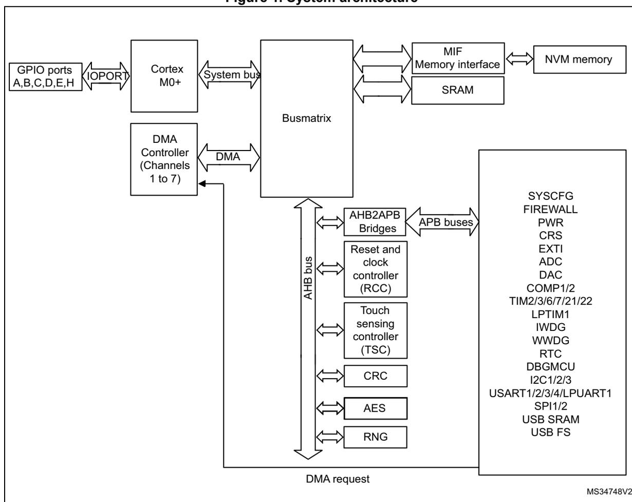
The diagram illustrates the system architecture of the STM32L0x2 microcontroller. At the center is the Busmatrix , which acts as a bridge between the system bus and the AHB bus. The Cortex M0+ core and the DMA Controller (Channels 1 to 7) are connected to the Busmatrix via the System bus and DMA respectively. The GPIO ports A,B,C,D,E,H are connected to the Cortex M0+ core via an IOPORT block. The Busmatrix is also connected to the MIF Memory interface and SRAM , which in turn connect to NVM memory . Below the Busmatrix, a vertical AHB bus connects to several functional blocks: Reset and clock controller (RCC) , Touch sensing controller (TSC) , CRC , AES , and RNG . These blocks are connected to a large block of APB buses via AHB2APB Bridges . The APB buses connect to a variety of peripherals listed in the diagram: SYSCFG , FIREWALL , PWR , CRS , EXTI , ADC , DAC , COMP1/2 , TIM2/3/6/7/21/22 , LPTIM1 , IWDG , WWDG , RTC , DBGMCU , I2C1/2/3 , USART1/2/3/4/LPUART1 , SPI1/2 , USB SRAM , and USB FS . A DMA request line is shown connecting the APB buses back to the DMA Controller. The diagram is labeled with the code MS34748V2 in the bottom right corner.
- 1. Refer to Table 1: STM32L0x2 memory density , to Table 2: Overview of features per category and to the device datasheets for the GPIO ports and peripherals available on your device.
2.1.1 S0: Cortex ® -bus
This bus connects the DCode/ICode bus of the Cortex ® -M0+ core to the BusMatrix. This bus is used by the core to fetch instructions, get data and access the AHB/APB resources.
2.1.2 S1: DMA-bus
This bus connects the AHB master interface of the DMA to the BusMatrix which manages the access of the different masters to Flash memory and data EEPROM, the SRAM and the AHB/APB peripherals.
2.1.3 BusMatrix
The BusMatrix manages the access arbitration between masters. The arbitration uses a Round Robin algorithm. The BusMatrix is composed of two masters (CPU, DMA) and three slaves (NVM interface, SRAM, AHB2APB1/2 bridges).
AHB/APB bridges
The AHB/APB bridge provide full synchronous connections between the AHB and the 2 APB buses. APB1 and APB2 operate at a maximum frequency of 32 MHz.
Refer to Section 2.2.2: Memory map and register boundary addresses on page 58 for the address mapping of the peripherals connected to this bridge.
After each device reset, all peripheral clocks are disabled (except for the SRAM and MIF). Before using a peripheral you have to enable its clock in the RCC_AHBENR, RCC_APB2ENR, RCC_APB1ENR or RCC_IOPENR register.
Note: When a 16- or 8-bit access is performed on an APB register, the access is transformed into a 32-bit access: the bridge duplicates the 16- or 8-bit data to feed the 32-bit vector.
2.2 Memory organization
2.2.1 Introduction
Program memory, data memory, registers and I/O ports are organized within the same linear 4-Gbyte address space.
The bytes are coded in memory in Little Endian format. The lowest numbered byte in a word is considered the word's least significant byte and the highest numbered byte the most significant.
The addressable memory space is divided into eight main blocks, of 512 Mbytes each.
2.2.2 Memory map and register boundary addresses
Figure 2. Memory map
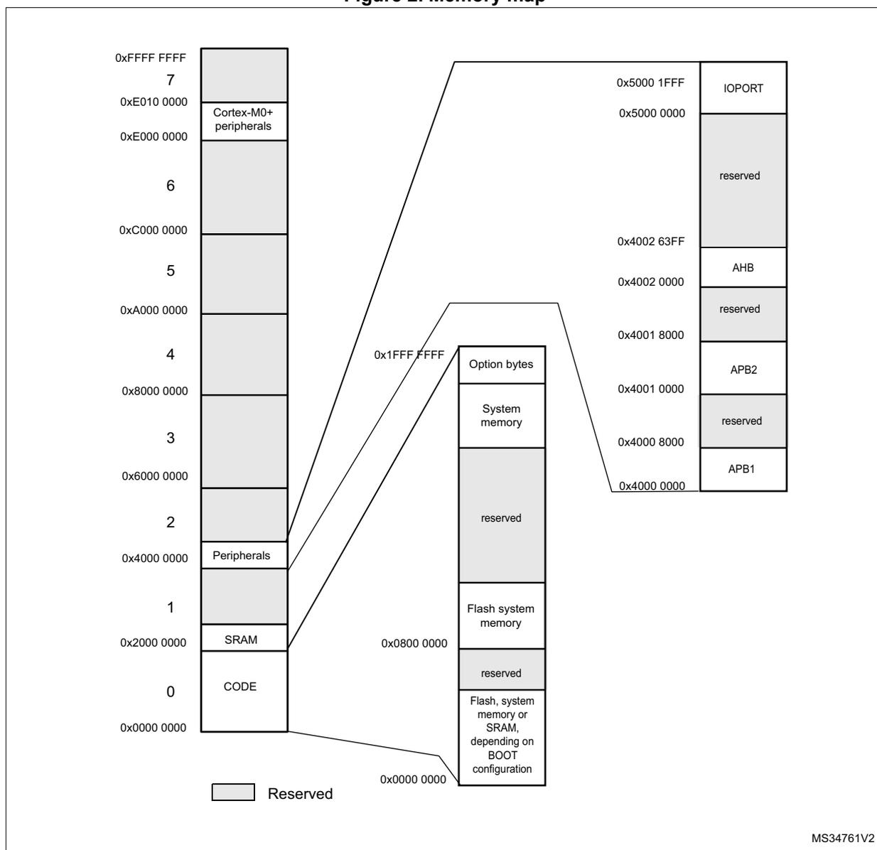
Memory map details:
- 0x0000 0000 to 0x2000 0000: CODE
- 0x2000 0000 to 0x4000 0000: SRAM
- 0x4000 0000 to 0x6000 0000: Peripherals
- 0x6000 0000 to 0x8000 0000: Reserved
- 0x8000 0000 to 0xA000 0000: Reserved
- 0xA000 0000 to 0xC000 0000: Reserved
- 0xC000 0000 to 0xE000 0000: Reserved
- 0xE000 0000 to 0xE010 0000: Cortex-M0+ peripherals
- 0xE010 0000 to 0xFFFF FFFF: Reserved
Zoomed-in view of 0x0000 0000 to 0x1FFF FFFF:
- 0x0000 0000 to 0x0800 0000: Flash, system memory or SRAM, depending on BOOT configuration
- 0x0800 0000 to 0x1000 0000: reserved
- 0x1000 0000 to 0x1800 0000: Flash system memory
- 0x1800 0000 to 0x2000 0000: reserved
- 0x2000 0000 to 0x2800 0000: System memory
- 0x2800 0000 to 0x3000 0000: Option bytes
Peripheral region (0x4000 0000 to 0x5000 1FFF):
- 0x4000 0000 to 0x4000 8000: APB1
- 0x4000 8000 to 0x4001 0000: reserved
- 0x4001 0000 to 0x4001 8000: APB2
- 0x4001 8000 to 0x4002 0000: reserved
- 0x4002 0000 to 0x4002 63FF: AHB
- 0x4002 63FF to 0x5000 0000: reserved
- 0x5000 0000 to 0x5000 1FFF: IOPORT
Legend: Reserved
MS34761V2
All the memory map areas that are not allocated to on-chip memories and peripherals are considered “Reserved”. For the detailed mapping of available memory and register areas, refer to the following table.
The following table gives the boundary addresses of the peripherals available in the devices.
Table 3. STM32L0x2 peripheral register boundary addresses (1)
| Bus | Boundary address | Size (bytes) | Peripheral | Peripheral register map |
|---|---|---|---|---|
| IOPORT | 0X5000 1C00 - 0X5000 1FFF | 1K | GPIOH | Section 9.4.12: GPIO register map |
| 0X5000 1400 - 0X5000 1BFF | 2 K | Reserved | - | |
| 0X5000 1000 - 0X5000 13FF | 1K | GPIOE | Section 9.4.12: GPIO register map | |
| 0X5000 0C00 - 0X5000 0FFF | 1K | GIOD | Section 9.4.12: GPIO register map | |
| 0X5000 0800 - 0X5000 0BFF | 1K | GPIO C | Section 9.4.12: GPIO register map | |
| 0X5000 0400 - 0X5000 07FF | 1K | GPIOB | Section 9.4.12: GPIO register map | |
| 0X5000 0000 - 0X5000 03FF | 1K | GPIOA | Section 9.4.12: GPIO register map | |
| AHB | 0X4002 6400 - 0X4002 FFFF | 49 K | Reserved | - |
| 0X4002 6000 - 0X4002 63FF | 1 K | AES (Cat 3 and 5 with AES only) | Section 18.7.13: AES register map | |
| 0X4002 5400 - 0X4002 5FFF | 3 K | Reserved | - | |
| 0X4002 5000 - 0X4002 53FF | 1 K | RNG | Section 19.7.4: RNG register map | |
| 0X4002 4400 - 0X4002 4FFF | 3 K | Reserved | - | |
| 0X4002 4000 - 0X4002 43FF | 1 K | TSC | Section 17.6.11: TSC register map | |
| 0X4002 3400 - 0X4002 43FF | 3 K | Reserved | - | |
| 0X4002 3000 - 0X4002 33FF | 1 K | CRC | Section 4.4.6: CRC register map | |
| 0X4002 2400 - 0X4002 2FFF | 3 K | Reserved | - | |
| 0X4002 2000 - 0X4002 23FF | 1 K | FLASH | Section 3.7.11: Flash register map | |
| 0X4002 1400 - 0X4002 1FFF | 3 K | Reserved | - | |
| 0X4002 1000 - 0X4002 13FF | 1 K | RCC | Section 7.3.22: RCC register map | |
| 0X4002 0400 - 0X4002 0FFF | 3 K | Reserved | - | |
| 0X4002 0000 - 0X4002 03FF | 1 K | DMA1 | Section 11.6.8: DMA register map |
| Bus | Boundary address | Size (bytes) | Peripheral | Peripheral register map |
|---|---|---|---|---|
| APB2 | 0X4001 5C00 - 0X4001 FFFF | 42 K | Reserved | - |
| 0X4001 5800 - 0X4001 5BFF | 1 K | DBG | Section 32.10: DBG register map | |
| 0X4001 3C00 - 0X4001 57FF | 7 K | Reserved | - | |
| 0X4001 3800 - 0X4001 3BFF | 1 K | USART1 | Section 28.8.12: USART register map | |
| 0X4001 3400 - 0X4001 37FF | 1 K | Reserved | - | |
| 0X4001 3000 - 0X4001 33FF | 1 K | SPI1 | Section 30.7.10: SPI register map | |
| 0X4001 2800 - 0X4001 2FFF | 2 K | Reserved | - | |
| 0X4001 2400 - 0X4001 27FF | 1 K | ADC1 | Section 14.12: ADC register map | |
| 0X4001 2000 - 0X4001 23FF | 1 K | Reserved | - | |
| 0X4001 1C00 - 0X4001 1FFF | 1 K | Firewall | Section 5.4.8: Firewall register map | |
| 0X4001 1800 - 0X4001 1BFF | 1 K | Reserved | - | |
| 0X4001 1400 - 0X4001 17FF | 1 K | TIM22 | Section 21.4.16: TIM21/22 register map | |
| 0X4001 0C000 - 0X4001 13FF | 2 K | Reserved | - | |
| 0X4001 0800 - 0X4001 0BFF | 1 K | TIM21 | Section 21.4.16: TIM21/22 register map | |
| 0X4001 0400 - 0X4001 07FF | 1 K | EXTI | Section 13.5.7: EXTI register map | |
| 0X4001 0000 - 0X4001 03FF | 1 K | SYSCFG, COMP | Section 10.2.8: SYSCFG register map, Section 16.5.3: COMP register map |
| Bus | Boundary address | Size (bytes) | Peripheral | Peripheral register map |
|---|---|---|---|---|
| APB1 | 0X4000 8000 - 0X4000 FFFF | 32 K | Reserved | - |
| 0X4000 7C00 - 0X4000 7FFF | 1 K | LPTIM1 | Section 23.7.9: LPTIM register map | |
| 0X4000 7800 - 0X4000 7BFF | 1K | I2C3 | Section 27.7.12: I2C register map | |
| 0X4000 7400 - 0X4000 77FF | 1 K | DAC1/2 | Section 15.10.15: DAC register map | |
| 0X4000 7000 - 0X4000 73FF | 1 K | PWR | Section 6.4.3: PWR register map | |
| 0X4000 6C00 - 0X4000 6FFF | 1 K | CRS | Section 8.7.5: CRS register map | |
| 0X4000 68000 - 0X4000 6BFF | 1 K | Reserved | - | |
| 0X4000 6000 - 0X4000 67FF | 2 K | USB (SRAM 512x16bit) | - | |
| 0X4000 5C00 - 0X4000 5FFF | 1 K | USB FS | Section 31.6.3: USB register map |
| Bus | Boundary address | Size (bytes) | Peripheral | Peripheral register map |
|---|---|---|---|---|
| APB1 | 0X4000 5800 - 0X4000 5BFF | 1 K | I2C2 | Section 27.7.12: I2C register map |
| 0X4000 5400 - 0X4000 57FF | 1 K | I2C1 | Section 27.7.12: I2C register map | |
| 0X4000 5000 - 0X4000 53FF | 1 K | USART5 | Section 28.8.12: USART register map | |
| 0X4000 4C00 - 0X4000 4FFF | 1 K | USART4 | Section 28.8.12: USART register map | |
| 0X4000 4800 - 0X4000 4BFF | 1 K | LPUART1 | Section 29.7.10: LPUART register map | |
| 0X4000 4400 - 0X4000 47FF | 1 K | USART2 | Section 28.8.12: USART register map | |
| 0X4000 3C00 - 0X4000 43FF | 2 K | Reserved | - | |
| 0X4000 3800 - 0X4000 3BFF | 1 K | SPI2 | Section 30.7.10: SPI register map | |
| 0X4000 3400 - 0X4000 37FF | 1 K | Reserved | - | |
| 0X4000 3000 - 0X4000 33FF | 1 K | IWDG | Section 24.4.6: IWDG register map | |
| 0X4000 2C00 - 0X4000 2FFF | 1 K | WWDG | Section 25.5.4: WWDG register map | |
| 0X4000 2800 - 0X4000 2BFF | 1 K | RTC + BKP_REG | Section 26.7.21: RTC register map | |
| 0X4000 1800 - 0X4000 27FF | 3 K | Reserved | - | |
| 0X4000 1400 - 0X4000 17FF | 1 K | TIMER7 | Section 22.4.9: TIM6/7 register map | |
| 0X4000 1000 - 0X4000 13FF | 1 K | TIMER6 | Section 22.4.9: TIM6/7 register map | |
| 0X4000 0800 - 0X4000 0FFF | 1 K | Reserved | - | |
| 0X4000 0400 - 0X4000 07FF | 1 K | TIMER3 | Section 20.5: TIMx register map | |
| 0X4000 0000 - 0X4000 03FF | 1 K | TIMER2 | Section 20.5: TIMx register map | |
| SRAM | 0X2000 2000 - 0X3FFF FFFF | ~524 M | Reserved | - |
| 0X2000 0000 - 0X2000 4FFF | up to 20 K | SRAM | - |
| Bus | Boundary address | Size (bytes) | Peripheral | Peripheral register map |
|---|---|---|---|---|
| NVM | 0x0800 0000 - 0x0802 FFFF | up to 192 K | Flash program memory | - |
| 0x0808 0000 - 0x0808 17FF | up to 6 K | Data EEPROM | - | |
| 0x1FF0 0000 - 0x1FF0 1FFF | 8 K | System memory | - | |
| 0x1FF8 0020 - 0x1FF8 007F | 96 | Factory option bytes | - | |
| 0x1FF8 0000 - 0x1FF8 001F | 32 | User option bytes | - |
- 1. Refer to Table 1: STM32L0x2 memory density , to Table 2: Overview of features per category and to the device datasheets for the GPIO ports and peripherals available on your device. The memory area corresponding to unavailable GPIO ports or peripherals are reserved.
2.3 Embedded SRAM
STM32L0x2 devices feature up to 20 Kbytes of static SRAM.
This RAM can be accessed as bytes, half-words (16 bits) or full words (32 bits). This memory can be addressed at maximum system clock frequency without wait state and thus by both CPU and DMA.
The SRAM start address is 0x2000 0000.
The CPU can access the SRAM from address 0x0000 0000 when physical remap is selected through boot pin or MEM_MODE (see Section 10.2.1: SYSCFG memory remap register (SYSCFG_CFGR1) ).
2.4 Boot configuration
In the STM32L0x2, three different boot modes can be selected through the BOOT0 pin and boot configuration bits in the User option byte, as shown in the following table.
Table 4. Boot modes (1)| Boot mode selection | Boot mode | Aliasings | |
|---|---|---|---|
| BOOT1 pin | BOOT0 pin | ||
| X | 0 | Flash program memory | Flash program memory is selected as boot area |
| 0 | 1 | System memory | System memory is selected as boot area |
| 1 | 1 | Embedded SRAM | Embedded SRAM is selected as boot area |
- 1. BOOT1 value is the opposite of nBOOT1 option bit.
The boot mode configuration is latched on the 4th rising edge of SYSCLK after reset. It is up to the user to set nBOOT1 and BOOT0 to select the required boot mode.
The boot mode configuration is also re-sampled when exiting from Standby mode. Consequently the boot mode configuration must not be modified in Standby mode. After this startup delay has elapsed, the CPU fetches the top-of-stack value from address 0x0000 0000, then starts code execution from the boot memory at 0x0000 0004.
Depending on the selected boot mode, Flash program memory, system memory or SRAM is accessible as follows:
- • Boot from Flash program memory: the Flash program memory is aliased in the boot memory space (0x0000 0000), but still accessible from its original memory space (0x0800 0000). In other words, the Flash memory contents can be accessed starting from address 0x0000 0000 or 0x0800 0000.
- • Boot from system memory: the system memory is aliased in the boot memory space (0x0000 0000), but still accessible from its original memory space (0x1FF0 0000).
- • Boot from the embedded SRAM: the SRAM is aliased in the boot memory space (0x0000 0000), but it is still accessible from its original memory space (0x2000 0000).
Bank swapping (category 5 devices only)
For devices featuring two banks, the bank swapping mechanism allows the CPU to point either to bank1 or to bank 2 in the boot memory space (0x0000 0000). Either Flash program and data EEPROM address are changed (see Table 8: NVM organization for UFB = 0 (128 Kbyte category 5 devices) , Table 10: NVM organization for UFB = 0 (64 Kbyte category 5 devices) ).
Physical remap
Once the boot pin and bit are selected, the application software can modify the memory accessible in the code area. This modification is performed by programming the MEM_MODE bits in the SYSCFG memory remap register (SYSCFG_CFGR1).
Embedded bootloader
The embedded bootloader is located in the System memory, programmed by ST during production. It is used to reprogram the Flash memory using one of the following serial interfaces:
- • For category 3 devices: USART1, USART2, SPI1 or SPI2
- • For category 5 devices with USB interface: USART1, USART2 or USB.
- • For category 5 devices without USB interface: USART1, USART2, SPI1, SPI2, I2C1 or I2C2.
For details concerning the bootloader serial interface corresponding I/O, refer to your device datasheet.
For further details on STM32 bootloader, please refer to AN2606.