22. USB on-the-go full-speed (OTG_FS)
22.1 OTG_FS introduction
Portions Copyright (c) 2004, 2005 Synopsys, Inc. All rights reserved. Used with permission.
This section presents the architecture and the programming model of the OTG_FS controller.
The following acronyms are used throughout this section:
| FS | Full-speed |
| LS | Low-speed |
| MAC | Media access controller |
| OTG | On-the-go |
| PFC | Packet FIFO controller |
| PHY | Physical layer |
| USB | Universal serial bus |
| UTMI | USB 2.0 transceiver macrocell interface (UTMI) |
References are made to the following documents:
- • USB On-The-Go Supplement, Revision 1.3
- • Universal Serial Bus Revision 2.0 Specification
The OTG_FS is a dual-role device (DRD) controller that supports both device and host functions and is fully compliant with the On-The-Go Supplement to the USB 2.0 Specification . It can also be configured as a host-only or device-only controller, fully compliant with the USB 2.0 Specification . In host mode, the OTG_FS supports full-speed (FS, 12 Mbits/s) and low-speed (LS, 1.5 Mbits/s) transfers whereas in device mode, it only supports full-speed (FS, 12 Mbits/s) transfers. The OTG_FS supports both HNP and SRP. The only external device required is a charge pump for \( V_{BUS} \) in host mode.
22.2 OTG_FS main features
The main features can be divided into three categories: general, host-mode and device-mode features.
22.2.1 General features
The OTG_FS interface general features are the following:
- • It is USB-IF certified to the Universal Serial Bus Specification Rev 2.0
- • It includes full support (PHY) for the optional On-The-Go (OTG) protocol detailed in the On-The-Go Supplement Rev 1.3 specification
- – Integrated support for A-B Device Identification (ID line)
- – Integrated support for host Negotiation Protocol (HNP) and Session Request Protocol (SRP)
- – It allows host to turn \( V_{BUS} \) off to conserve battery power in OTG applications
- – It supports OTG monitoring of \( V_{BUS} \) levels with internal comparators
- – It supports dynamic host-peripheral switch of role
- • It is software-configurable to operate as:
- – SRP capable USB FS Peripheral (B-device)
- – SRP capable USB FS/LS host (A-device)
- – USB On-The-Go Full-Speed Dual Role device
- • It supports FS SOF and LS Keep-alives with
- – SOF pulse PAD connectivity (OTG_FS_SOF)
- – SOF pulse internal connection to timer2 (TIM2)
- – Configurable framing period
- – Configurable end of frame interrupt
- • It includes power saving features such as system stop during USB Suspend, switch-off of clock domains internal to the digital core, PHY and DFIFO power management
- • It features a dedicated RAM of 1.25 Kbytes with advanced FIFO control:
- – Configurable partitioning of RAM space into different FIFOs for flexible and efficient use of RAM
- – Each FIFO can hold multiple packets
- – Dynamic memory allocation
- – Configurable FIFO sizes that are not powers of 2 to allow the use of contiguous memory locations
- • It guarantees max USB bandwidth for up to one frame (1ms) without system intervention
22.2.2 Host-mode features
The OTG_FS interface main features and requirements in host-mode are the following:
- • External charge pump for V BUS voltage generation.
- • Up to 8 host channels (pipes): each channel is dynamically reconfigurable to allocate any type of USB transfer.
- • Built-in hardware scheduler holding:
- – Up to 8 interrupt plus isochronous transfer requests in the periodic hardware queue
- – Up to 8 control plus bulk transfer requests in the non-periodic hardware queue
- • Management of a shared RX FIFO, a periodic TX FIFO and a nonperiodic TX FIFO for efficient usage of the USB data RAM.
22.2.3 Peripheral-mode features
The OTG_FS interface main features in peripheral-mode are the following:
- • 1 bidirectional control endpoint0
- • 3 IN endpoints (EPs) configurable to support Bulk, Interrupt or Isochronous transfers
- • 3 OUT endpoints configurable to support Bulk, Interrupt or Isochronous transfers
- • Management of a shared Rx FIFO and a Tx-OUT FIFO for efficient usage of the USB data RAM
- • Management of up to 4 dedicated Tx-IN FIFOs (one for each active IN EP) to put less load on the application
- • Support for the soft disconnect feature.
22.3 OTG_FS functional description
Figure 242. OTG full-speed block diagram
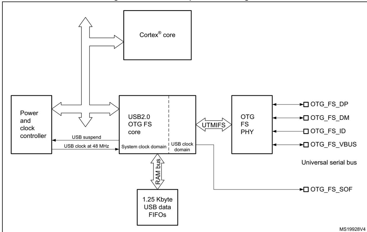
MS19928V4
22.3.1 OTG pins
Table 126. OTG_FS input/output pins
| Signal name | Signal type | Description |
|---|---|---|
| OTG_FS_DP | Digital input/output | USB OTG D+ line |
| OTG_FS_DM | Digital input/output | USB OTG D- line |
| OTG_FS_ID | Digital input | USB OTG ID |
| OTG_FS_VBUS | Analog input | USB OTG VBUS |
| OTG_FS_SOF | Digital output | USB OTG Start Of Frame (visibility) |
22.3.2 OTG full-speed core
The USB OTG FS receives the 48 MHz \( \pm 0.25\% \) clock from the reset and clock controller (RCC), via an external quartz. The USB clock is used for driving the 48 MHz domain at full-speed (12 Mbit/s) and must be enabled prior to configuring the OTG FS core.
The CPU reads and writes from/to the OTG FS core registers through the AHB peripheral bus. It is informed of USB events through the single USB OTG interrupt line described in Section 22.15: OTG_FS interrupts .
The CPU submits data over the USB by writing 32-bit words to dedicated OTG_FS locations (push registers). The data are then automatically stored into Tx-data FIFOs configured within the USB data RAM. There is one Tx-FIFO push register for each in-endpoint (peripheral mode) or out-channel (host mode).
The CPU receives the data from the USB by reading 32-bit words from dedicated OTG_FS addresses (pop registers). The data are then automatically retrieved from a shared Rx-FIFO configured within the 1.25 KB USB data RAM. There is one Rx-FIFO pop register for each out-endpoint or in-channel.
The USB protocol layer is driven by the serial interface engine (SIE) and serialized over the USB by the full-/low-speed transceiver module within the on-chip physical layer (PHY).
22.3.3 Full-speed OTG PHY
The embedded full-speed OTG PHY is controlled by the OTG FS core and conveys USB control & data signals through the full-speed subset of the UTMI+ Bus (UTMIFS). It provides the physical support to USB connectivity.
The full-speed OTG PHY includes the following components:
- • FS/LS transceiver module used by both host and device. It directly drives transmission and reception on the single-ended USB lines.
- • integrated ID pull-up resistor used to sample the ID line for A/B device identification.
- • DP/DM integrated pull-up and pull-down resistors controlled by the OTG_FS core depending on the current role of the device. As a peripheral, it enables the DP pull-up resistor to signal full-speed peripheral connections as soon as \( V_{BUS} \) is sensed to be at a valid level (B-session valid). In host mode, pull-down resistors are enabled on both DP/DM. Pull-up and pull-down resistors are dynamically switched when the device’s role is changed via the host negotiation protocol (HNP).
- • Pull-up/pull-down resistor ECN circuit. The DP pull-up consists of 2 resistors controlled separately from the OTG_FS as per the resistor Engineering Change Notice applied to USB Rev2.0. The dynamic trimming of the DP pull-up strength allows for better noise rejection and Tx/Rx signal quality.
- • \( V_{BUS} \) sensing comparators with hysteresis used to detect \( V_{BUS} \) Valid, A-B Session Valid and session-end voltage thresholds. They are used to drive the session request protocol (SRP), detect valid startup and end-of-session conditions, and constantly monitor the \( V_{BUS} \) supply during USB operations.
- • \( V_{BUS} \) pulsing method circuit used to charge/discharge \( V_{BUS} \) through resistors during the SRP (weak drive).
Caution: To guarantee a correct operation for the USB OTG FS peripheral, the AHB frequency should be higher than 14.2 MHz.
22.4 OTG dual role device (DRD)
Figure 243. OTG A-B device connection
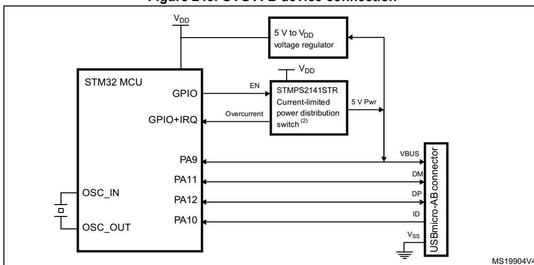
- 1. External voltage regulator only needed when building a \( V_{BUS} \) powered device
- 2. STMP2141STR needed only if the application has to support a \( V_{BUS} \) powered device. A basic power switch can be used if 5 V are available on the application board.
22.4.1 ID line detection
The host or peripheral (the default) role is assumed depending on the ID input pin (OTG_FS_ID). The ID line status is determined on plugging in the USB, depending on which side of the USB cable is connected to the micro-AB receptacle.
- • If the B-side of the USB cable is connected with a floating ID wire, the integrated pull-up resistor detects a high ID level and the default Peripheral role is confirmed. In this configuration the OTG_FS complies with the standard FSM described by section 6.8.2: On-The-Go B-device of the On-The-Go Specification Rev1.3 supplement to the USB2.0.
- • If the A-side of the USB cable is connected with a grounded ID, the OTG_FS issues an ID line status change interrupt (CIDSCHG bit in OTG_FS_GINTSTS) for host software initialization, and automatically switches to the host role. In this configuration the OTG_FS complies with the standard FSM described by section 6.8.1: On-The-Go A-device of the On-The-Go Specification Rev1.3 supplement to the USB2.0.
22.4.2 HNP dual role device
The HNP capable bit in the Global USB configuration register (HNPCAP bit in OTG_FS_GUSBCFG) enables the OTG_FS core to dynamically change its role from A-host to A-peripheral and vice-versa, or from B-Peripheral to B-host and vice-versa according to the host negotiation protocol (HNP). The current device status can be read by the combined values of the Connector ID Status bit in the Global OTG control and status register (CIDSTS bit in OTG_FS_GOTGCTL) and the current mode of operation bit in the global interrupt and status register (CMOD bit in OTG_FS_GINTSTS).
The HNP program model is described in detail in Section 22.17: OTG_FS programming model .
22.4.3 SRP dual role device
The SRP capable bit in the global USB configuration register (SRPCAP bit in OTG_FS_GUSBCFG) enables the OTG_FS core to switch off the generation of \( V_{BUS} \) for the A-device to save power. Note that the A-device is always in charge of driving \( V_{BUS} \) regardless of the host or peripheral role of the OTG_FS.
the SRP A/B-device program model is described in detail in Section 22.17: OTG_FS programming model .
22.5 USB peripheral
This section gives the functional description of the OTG_FS in the USB peripheral mode. The OTG_FS works as an USB peripheral in the following circumstances:
- • OTG B-Peripheral
- – OTG B-device default state if B-side of USB cable is plugged in
- • OTG A-Peripheral
- – OTG A-device state after the HNP switches the OTG_FS to its peripheral role
- • B-device
- – If the ID line is present, functional and connected to the B-side of the USB cable, and the HNP-capable bit in the Global USB Configuration register (HNPCAP bit in OTG_FS_GUSBCFG) is cleared (see On-The-Go Rev1.3 par. 6.8.3).
- • Peripheral only (see
Figure 244: USB peripheral-only connection
)
- – The force device mode bit in the Global USB configuration register (FDMOD in OTG_FS_GUSBCFG) is set to 1, forcing the OTG_FS core to work as a USB peripheral-only (see On-The-Go Rev1.3 par. 6.8.3). In this case, the ID line is ignored even if present on the USB connector.
Note: To build a bus-powered device implementation in case of the B-device or peripheral-only configuration, an external regulator has to be added that generates the \( V_{DD} \) chip-supply from \( V_{BUS} \) .
The \( V_{BUS} \) pin can be freed by disabling the \( V_{BUS} \) sensing option. This is done by setting the NOVBUSSENS bit in the OTG_FS_GCCFG register. In this case the \( V_{BUS} \) is considered internally to be always at \( V_{BUS} \) valid level (5 V).
Figure 244. USB peripheral-only connection
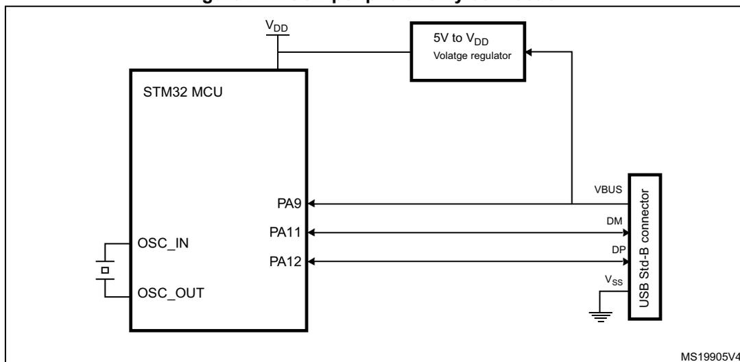
- 1. Use a regulator to build a bus-powered device.
22.5.1 SRP-capable peripheral
The SRP capable bit in the Global USB configuration register (SRPCAP bit in OTG_FS_GUSBCFG) enables the OTG_FS to support the session request protocol (SRP). In this way, it allows the remote A-device to save power by switching off \( V_{BUS} \) while the USB session is suspended.
The SRP peripheral mode program model is described in detail in the B-device session request protocol section.
22.5.2 Peripheral states
Powered state
The \( V_{BUS} \) input detects the B-Session valid voltage by which the USB peripheral is allowed to enter the powered state (see USB2.0 par9.1). The OTG_FS then automatically connects the DP pull-up resistor to signal full-speed device connection to the host and generates the session request interrupt (SRQINT bit in OTG_FS_GINTSTS) to notify the powered state.
The \( V_{BUS} \) input also ensures that valid \( V_{BUS} \) levels are supplied by the host during USB operations. If a drop in \( V_{BUS} \) below B-session valid happens to be detected (for instance because of a power disturbance or if the host port has been switched off), the OTG_FS automatically disconnects and the session end detected (SEDET bit in OTG_FS_GOTGINT) interrupt is generated to notify that the OTG_FS has exited the powered state.
In the powered state, the OTG_FS expects to receive some reset signaling from the host. No other USB operation is possible. When a reset signaling is received the reset detected interrupt (USBRST in OTG_FS_GINTSTS) is generated. When the reset signaling is complete, the enumeration done interrupt (ENUMDNE bit in OTG_FS_GINTSTS) is generated and the OTG_FS enters the Default state.
Soft disconnect
The powered state can be exited by software with the soft disconnect feature. The DP pull-up resistor is removed by setting the soft disconnect bit in the device control register (SDIS bit in OTG_FS_DCTL), causing a device disconnect detection interrupt on the host side even though the USB cable was not really removed from the host port.
Default state
In the Default state the OTG_FS expects to receive a SET_ADDRESS command from the host. No other USB operation is possible. When a valid SET_ADDRESS command is decoded on the USB, the application writes the corresponding number into the device address field in the device configuration register (DAD bit in OTG_FS_DCFG). The OTG_FS then enters the address state and is ready to answer host transactions at the configured USB address.
Suspended state
The OTG_FS peripheral constantly monitors the USB activity. After counting 3 ms of USB idleness, the early suspend interrupt (ESUSP bit in OTG_FS_GINTSTS) is issued, and confirmed 3 ms later, if appropriate, by the suspend interrupt (USBSUSP bit in OTG_FS_GINTSTS). The device suspend bit is then automatically set in the device status register (SUSPSTS bit in OTG_FS_DSTS) and the OTG_FS enters the suspended state.
The suspended state may optionally be exited by the device itself. In this case the application sets the remote wake-up signaling bit in the device control register (RWUSIG bit in OTG_FS_DCTL) and clears it after 1 to 15 ms.
When a resume signaling is detected from the host, the resume interrupt (WKUPINT bit in OTG_FS_GINTSTS) is generated and the device suspend bit is automatically cleared.
22.5.3 Peripheral endpoints
The OTG_FS core instantiates the following USB endpoints:
- • Control endpoint 0:
- – Bidirectional and handles control messages only
- – Separate set of registers to handle in and out transactions
- – Proper control (OTG_FS_DIEPCTL0/OTG_FS_DOEPCTL0), transfer configuration (OTG_FS_DIEPTSIZ0/OTG_FS_DOEPTSIZ0), and status-interrupt (OTG_FS_DIEPINTx/OTG_FS_DOEPINT0) registers. The available set of bits inside the control and transfer size registers slightly differs from that of other endpoints
- • 3 IN endpoints
- – Each of them can be configured to support the isochronous, bulk or interrupt transfer type
- – Each of them has proper control (OTG_FS_DIEPCTLx), transfer configuration (OTG_FS_DIEPTSIZx), and status-interrupt (OTG_FS_DIEPINTx) registers
- – The Device IN endpoints common interrupt mask register (OTG_FS_DIEPMSK) is available to enable/disable a single kind of endpoint interrupt source on all of the IN endpoints (EP0 included)
- – Support for incomplete isochronous IN transfer interrupt (IISOIXFR bit in OTG_FS_GINTSTS), asserted when there is at least one isochronous IN endpoint
on which the transfer is not completed in the current frame. This interrupt is asserted along with the end of periodic frame interrupt (OTG_FS_GINTSTS/EOPF).
- • 3 OUT endpoints
- – Each of them can be configured to support the isochronous, bulk or interrupt transfer type
- – Each of them has a proper control (OTG_FS_DOEPCTLx), transfer configuration (OTG_FS_DOEPTSIZx) and status-interrupt (OTG_FS_DOEPINTx) register
- – Device Out endpoints common interrupt mask register (OTG_FS_DOEPMSK) is available to enable/disable a single kind of endpoint interrupt source on all of the OUT endpoints (EP0 included)
- – Support for incomplete isochronous OUT transfer interrupt (INCOMPISOOUT bit in OTG_FS_GINTSTS), asserted when there is at least one isochronous OUT endpoint on which the transfer is not completed in the current frame. This interrupt is asserted along with the end of periodic frame interrupt (OTG_FS_GINTSTS/EOPF).
Endpoint control
- • The following endpoint controls are available to the application through the device endpoint-x IN/OUT control register (DIEPCTLx/DOEPCTLx):
- – Endpoint enable/disable
- – Endpoint activate in current configuration
- – Program USB transfer type (isochronous, bulk, interrupt)
- – Program supported packet size
- – Program Tx-FIFO number associated with the IN endpoint
- – Program the expected or transmitted data0/data1 PID (bulk/interrupt only)
- – Program the even/odd frame during which the transaction is received or transmitted (isochronous only)
- – Optionally program the NAK bit to always negative-acknowledge the host regardless of the FIFO status
- – Optionally program the STALL bit to always stall host tokens to that endpoint
- – Optionally program the SNOOP mode for OUT endpoint not to check the CRC field of received data
Endpoint transfer
The device endpoint-x transfer size registers (DIEPTSIZx/DOEPTSIZx) allow the application to program the transfer size parameters and read the transfer status. Programming must be done before setting the endpoint enable bit in the endpoint control register. Once the endpoint is enabled, these fields are read-only as the OTG FS core updates them with the current transfer status.
The following transfer parameters can be programmed:
- • Transfer size in bytes
- • Number of packets that constitute the overall transfer size
Endpoint status/interrupt
The device endpoint-x interrupt registers (DIEPINTx/DOEPINTx) indicate the status of an endpoint with respect to USB- and AHB-related events. The application must read these registers when the OUT endpoint interrupt bit or the IN endpoint interrupt bit in the core interrupt register (OEPINT bit in OTG_FS_GINTSTS or IEPINT bit in OTG_FS_GINTSTS, respectively) is set. Before the application can read these registers, it must first read the device all endpoints interrupt (OTG_FS_DAINT) register to get the exact endpoint number for the device endpoint-x interrupt register. The application must clear the appropriate bit in this register to clear the corresponding bits in the DAINT and GINTSTS registers
The peripheral core provides the following status checks and interrupt generation:
- • Transfer completed interrupt, indicating that data transfer was completed on both the application (AHB) and USB sides
- • Setup stage has been done (control-out only)
- • Associated transmit FIFO is half or completely empty (in endpoints)
- • NAK acknowledge has been transmitted to the host (isochronous-in only)
- • IN token received when Tx-FIFO was empty (bulk-in/interrupt-in only)
- • Out token received when endpoint was not yet enabled
- • Babble error condition has been detected
- • Endpoint disable by application is effective
- • Endpoint NAK by application is effective (isochronous-in only)
- • More than 3 back-to-back setup packets were received (control-out only)
- • Timeout condition detected (control-in only)
- • Isochronous out packet has been dropped, without generating an interrupt
22.6 USB host
This section gives the functional description of the OTG_FS in the USB host mode. The OTG_FS works as a USB host in the following circumstances:
- • OTG A-host
- – OTG A-device default state when the A-side of the USB cable is plugged in
- • OTG B-host
- – OTG B-device after HNP switching to the host role
- • A-device
- – If the ID line is present, functional and connected to the A-side of the USB cable, and the HNP-capable bit is cleared in the Global USB Configuration register (HNP CAP bit in OTG_FS_GUSBCFG). Integrated pull-down resistors are automatically set on the DP/DM lines.
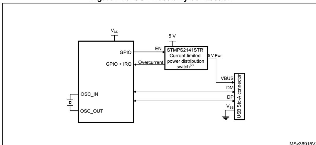
- • Host only (see
Figure 245: USB host-only connection
).
- – The force host mode bit in the global USB configuration register (FHMOD bit in OTG_FS_GUSBCFG) forces the OTG_FS core to work as a USB host-only. In this case, the ID line is ignored even if present on the USB connector. Integrated pull-down resistors are automatically set on the DP/DM lines.
Note: On-chip 5 V \( V_{BUS} \) generation is not supported. For this reason, a charge pump or, if 5 V are available on the application board, a basic power switch must be added externally to drive
the 5 V \( V_{BUS} \) line. The external charge pump can be driven by any GPIO output. This is required for the OTG A-host, A-device and host-only configurations.
The \( V_{BUS} \) input ensures that valid \( V_{BUS} \) levels are supplied by the charge pump during USB operations while the charge pump overcurrent output can be input to any GPIO pin configured to generate port interrupts. The overcurrent ISR must promptly disable the \( V_{BUS} \) generation.
Figure 245. USB host-only connection
graph LR
    subgraph MCU [STM32 Microcontroller]
        VDD
        GPIO
        GPIO_IRQ[GPIO + IRQ]
        OSC_IN
        OSC_OUT
        DM_MCU[DM]
        DP_MCU[DP]
    end

    subgraph Switch [STMP2141STR Switch]
        EN
        OC[Overcurrent]
        PWR_IN[5 V]
        PWR_OUT[5 V Pwr]
    end

    subgraph USB [USB Std-A connector]
        VBUS
        DM_USB[DM]
        DP_USB[DP]
        VSS
    end

    VDD --- 5V_Source[VDD]
    GPIO --> EN
    OC --> GPIO_IRQ
    PWR_IN --- 5V_Source2[5 V]
    PWR_OUT --> VBUS
    DM_MCU <--> DM_USB
    DP_MCU <--> DP_USB
    OSC_IN --- Crystal
    OSC_OUT --- Crystal
    VSS --- GND[Ground]
- 1. STMP2141STR needed only if the application has to support a \( V_{BUS} \) powered device. A basic power switch can be used if 5 V are available on the application board.
- 2. \( V_{DD} \) range is between 2 V and 3.6 V.
22.6.1 SRP-capable host
SRP support is available through the SRP capable bit in the global USB configuration register (SRPCAP bit in OTG_FS_GUSBCFG). With the SRP feature enabled, the host can save power by switching off the \( V_{BUS} \) power while the USB session is suspended.
The SRP host mode program model is described in detail in the A-device session request protocol section.
22.6.2 USB host states
Host port power
On-chip 5 V \( V_{BUS} \) generation is not supported. For this reason, a charge pump or, if 5 V are available on the application board, a basic power switch, must be added externally to drive the 5 V \( V_{BUS} \) line. The external charge pump can be driven by any GPIO output. When the application decides to power on \( V_{BUS} \) using the chosen GPIO, it must also set the port power bit in the host port control and status register (PPWR bit in OTG_FS_HPRT).
\( V_{BUS} \) valid
When HNP or SRP is enabled the VBUS sensing pin (PA9) pin should be connected to \( V_{BUS} \) . The \( V_{BUS} \) input ensures that valid \( V_{BUS} \) levels are supplied by the charge pump during USB operations. Any unforeseen \( V_{BUS} \) voltage drop below the \( V_{BUS} \) valid threshold (4.25 V) leads to an OTG interrupt triggered by the session end detected bit (SEDET bit in
OTG_FS_GOTGINT). The application is then required to remove the \( V_{BUS} \) power and clear the port power bit.
When HNP and SRP are both disabled, the VBUS sensing pin (PA9) should not be connected to \( V_{BUS} \) . This pin can be used as GPIO.
The charge pump overcurrent flag can also be used to prevent electrical damage. Connect the overcurrent flag output from the charge pump to any GPIO input and configure it to generate a port interrupt on the active level. The overcurrent ISR must promptly disable the \( V_{BUS} \) generation and clear the port power bit.
Host detection of a peripheral connection
If SRP or HNP are enabled, even if USB peripherals or B-devices can be attached at any time, the OTG_FS does not detect any bus connection. When \( V_{BUS} \) is at a valid level and a remote B-device is attached, the OTG_FS core issues a host port interrupt triggered by the device connected bit in the host port control and status register (PCDET bit in OTG_FS_HPRT).
When HNP and SRP are both disabled, USB peripherals or B-device are detected as soon as they are connected. The OTG_FS core issues a host port interrupt triggered by the device connected bit in the host port control and status (PCDET bit in OTG_FS_HPRT).
Host detection of peripheral a disconnection
The peripheral disconnection event triggers the disconnect detected interrupt (DISCINT bit in OTG_FS_GINTSTS).
Host enumeration
After detecting a peripheral connection the host must start the enumeration process by sending USB reset and configuration commands to the new peripheral.
Before starting to drive a USB reset, the application waits for the OTG interrupt triggered by the debounce done bit (DBCDNE bit in OTG_FS_GOTGINT), which indicates that the bus is stable again after the electrical debounce caused by the attachment of a pull-up resistor on DP (FS) or DM (LS).
The application drives a USB reset signaling (single-ended zero) over the USB by keeping the port reset bit set in the host port control and status register (PRST bit in OTG_FS_HPRT) for a minimum of 10 ms and a maximum of 20 ms. The application takes care of the timing count and then of clearing the port reset bit.
Once the USB reset sequence has completed, the host port interrupt is triggered by the port enable/disable change bit (PENCHNG bit in OTG_FS_HPRT). This informs the application that the speed of the enumerated peripheral can be read from the port speed field in the host port control and status register (PSPD bit in OTG_FS_HPRT) and that the host is starting to drive SOFs (FS) or Keep alives (LS). The host is now ready to complete the peripheral enumeration by sending peripheral configuration commands.
Host suspend
The application decides to suspend the USB activity by setting the port suspend bit in the host port control and status register (PSUSP bit in OTG_FS_HPRT). The OTG_FS core stops sending SOFs and enters the suspended state.
The suspended state can be optionally exited on the remote device's initiative (remote wake-up). In this case the remote wake-up interrupt (WKUPINT bit in OTG_FS_GINTSTS)
is generated upon detection of a remote wake-up signaling, the port resume bit in the host port control and status register (PRES bit in OTG_FS_HPRT) self-sets, and resume signaling is automatically driven over the USB. The application must time the resume window and then clear the port resume bit to exit the suspended state and restart the SOF.
If the suspended state is exited on the host initiative, the application must set the port resume bit to start resume signaling on the host port, time the resume window and finally clear the port resume bit.
22.6.3 Host channels
The OTG_FS core instantiates 8 host channels. Each host channel supports an USB host transfer (USB pipe). The host is not able to support more than 8 transfer requests at the same time. If more than 8 transfer requests are pending from the application, the host controller driver (HCD) must re-allocate channels when they become available from previous duty, that is, after receiving the transfer completed and channel halted interrupts.
Each host channel can be configured to support in/out and any type of periodic/nonperiodic transaction. Each host channel makes use of proper control (HCCHARx), transfer configuration (HCTSIZx) and status/interrupt (HCINTx) registers with associated mask (HCINTMSKx) registers.
Host channel control
- • The following host channel controls are available to the application through the host channel-x characteristics register (HCCHARx):
- – Channel enable/disable
- – Program the FS/LS speed of target USB peripheral
- – Program the address of target USB peripheral
- – Program the endpoint number of target USB peripheral
- – Program the transfer IN/OUT direction
- – Program the USB transfer type (control, bulk, interrupt, isochronous)
- – Program the maximum packet size (MPS)
- – Program the periodic transfer to be executed during odd/even frames
Host channel transfer
The host channel transfer size registers (HCTSIZx) allow the application to program the transfer size parameters, and read the transfer status. Programming must be done before setting the channel enable bit in the host channel characteristics register. Once the endpoint is enabled the packet count field is read-only as the OTG_FS core updates it according to the current transfer status.
- • The following transfer parameters can be programmed:
- – transfer size in bytes
- – number of packets making up the overall transfer size
- – initial data PID
Host channel status/interrupt
The host channel-x interrupt register (HCINTx) indicates the status of an endpoint with respect to USB- and AHB-related events. The application must read these registers when the host channels interrupt bit in the core interrupt register (HCINT bit in OTG_FS_GINTSTS) is
set. Before the application can read these registers, it must first read the host all channels interrupt (HCAINT) register to get the exact channel number for the host channel-x interrupt register. The application must clear the appropriate bit in this register to clear the corresponding bits in the HAINT and GINTSTS registers. The mask bits for each interrupt source of each channel are also available in the OTG_FS_HCINTMSK-x register.
- • The host core provides the following status checks and interrupt generation:
- – Transfer completed interrupt, indicating that the data transfer is complete on both the application (AHB) and USB sides
- – Channel has stopped due to transfer completed, USB transaction error or disable command from the application
- – Associated transmit FIFO is half or completely empty (IN endpoints)
- – ACK response received
- – NAK response received
- – STALL response received
- – USB transaction error due to CRC failure, timeout, bit stuff error, false EOP
- – Babble error
- – fraMe overrun
- – dAta toggle error
22.6.4 Host scheduler
The host core features a built-in hardware scheduler which is able to autonomously re-order and manage the USB transaction requests posted by the application. At the beginning of each frame the host executes the periodic (isochronous and interrupt) transactions first, followed by the nonperiodic (control and bulk) transactions to achieve the higher level of priority granted to the isochronous and interrupt transfer types by the USB specification.
The host processes the USB transactions through request queues (one for periodic and one for nonperiodic). Each request queue can hold up to 8 entries. Each entry represents a pending transaction request from the application, and holds the IN or OUT channel number along with other information to perform a transaction on the USB. The order in which the requests are written to the queue determines the sequence of the transactions on the USB interface.
At the beginning of each frame, the host processes the periodic request queue first, followed by the nonperiodic request queue. The host issues an incomplete periodic transfer interrupt (IPXFR bit in OTG_FS_GINTSTS) if an isochronous or interrupt transaction scheduled for the current frame is still pending at the end of the current frame. The OTG HS core is fully responsible for the management of the periodic and nonperiodic request queues. The periodic transmit FIFO and queue status register (HPTXSTS) and nonperiodic transmit FIFO and queue status register (HNPTXSTS) are read-only registers which can be used by the application to read the status of each request queue. They contain:
- • The number of free entries currently available in the periodic (nonperiodic) request queue (8 max)
- • Free space currently available in the periodic (nonperiodic) Tx-FIFO (out-transactions)
- • IN/OUT token, host channel number and other status information.
As request queues can hold a maximum of 8 entries each, the application can push to schedule host transactions in advance with respect to the moment they physically reach the
SB for a maximum of 8 pending periodic transactions plus 8 pending nonperiodic transactions.
To post a transaction request to the host scheduler (queue) the application must check that there is at least 1 entry available in the periodic (nonperiodic) request queue by reading the PTXQSAV bits in the OTG_FS_HNPTXSTS register or NPTQXSAV bits in the OTG_FS_HNPTXSTS register.
22.7 SOF trigger
Figure 246. SOF connectivity
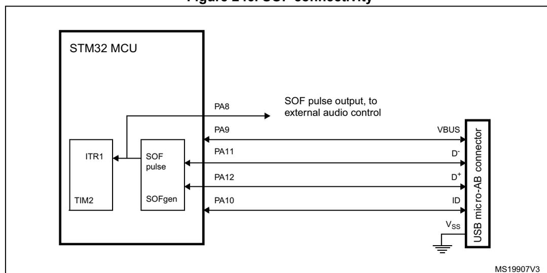
The diagram illustrates the SOF connectivity within an STM32 MCU and its connection to a USB micro-AB connector. Inside the MCU, the SOF pulse is generated by the SOFgen block and is connected to the ITR1 input of the TIM2 timer. The SOF pulse output is also connected to the PA8 pin, which is labeled 'SOF pulse output, to external audio control'. The USB micro-AB connector is connected to the MCU via several pins: PA9 (VBUS), PA11 (D-), PA12 (D+), and PA10 (ID). The Vss pin of the connector is connected to ground. The diagram is labeled with the code MS19907V3.
The OTG FS core provides means to monitor, track and configure SOF framing in the host and peripheral, as well as an SOF pulse output connectivity feature.
Such utilities are especially useful for adaptive audio clock generation techniques, where the audio peripheral needs to synchronize to the isochronous stream provided by the PC, or the host needs to trim its framing rate according to the requirements of the audio peripheral.
22.7.1 Host SOFs
In host mode the number of PHY clocks occurring between the generation of two consecutive SOF (FS) or Keep-alive (LS) tokens is programmable in the host frame interval register (HFIR), thus providing application control over the SOF framing period. An interrupt is generated at any start of frame (SOF bit in OTH_FS_GINTSTS). The current frame number and the time remaining until the next SOF are tracked in the host frame number register (HFNUM).
An SOF pulse signal, generated at any SOF starting token and with a width of 20 HCLK cycles, can be made available externally on the OTG_FS_SOF pin using the SOFOUTEN bit in the global control and configuration register. The SOF pulse is also internally connected to the input trigger of timer 2 (TIM2), so that the input capture feature, the output compare feature and the timer can be triggered by the SOF pulse. The TIM2 connection is enabled register.
22.7.2 Peripheral SOFs
In device mode, the start of frame interrupt is generated each time an SOF token is received on the USB (SOF bit in OTH_FS_GINTSTS). The corresponding frame number can be read from the device status register (FNSOF bit in OTG_FS_DSTS). An SOF pulse signal with a width of 20 HCLK cycles is also generated and can be made available externally on the OTG_FS_SOF pin by using the SOF output enable bit in the global control and configuration register (SOFOUTEN bit in OTG_FS_GCCFG). The SOF pulse signal is also internally connected to the TIM2 input trigger, so that the input capture feature, the output compare feature and the timer can be triggered by the SOF pulse. The TIM2 connection is enabled .
The end of periodic frame interrupt (GINTSTS/EOPF) is used to notify the application when 80%, 85%, 90% or 95% of the time frame interval elapsed depending on the periodic frame interval field in the device configuration register (PFIVL bit in OTG_FS_DCFG). This feature can be used to determine if all of the isochronous traffic for that frame is complete.
22.8 OTG low-power modes
Table 127 below defines the STM32 low power modes and their compatibility with the OTG.
Table 127. Compatibility of STM32 low power modes with the OTG
| Mode | Description | USB compatibility |
|---|---|---|
| Run | MCU fully active | Required when USB not in suspend state. |
| Sleep | USB suspend exit causes the device to exit Sleep mode. Peripheral registers content is kept. | Available while USB is in suspend state. |
| Stop | USB suspend exit causes the device to exit Stop mode. Peripheral registers content is kept (1) . | Available while USB is in suspend state. |
| Standby | Powered-down. The peripheral must be reinitialized after exiting Standby mode. | Not compatible with USB applications. |
- 1. Within Stop mode there are different possible settings. Some restrictions may also exist, please refer to Section 5: Power controller (PWR) to understand which (if any) restrictions apply when using OTG.
The power consumption of the OTG PHY is controlled by three bits in the general core configuration register:
- • PHY power down (GCCFG/PWRDWN)
It switches on/off the full-speed transceiver module of the PHY. It must be preliminarily set to allow any USB operation. - • A-V
BUS
sensing enable (GCCFG/VBUSASEN)
It switches on/off the V BUS comparators associated with A-device operations. It must be set when in A-device (USB host) mode and during HNP. - • B-V
BUS
sensing enable (GCCFG/VBUSASEN)
It switches on/off the V BUS comparators associated with B-device operations. It must be set when in B-device (USB peripheral) mode and during HNP.
Power reduction techniques are available while in the USB suspended state, when the USB session is not yet valid or the device is disconnected.
- • Stop PHY clock (STPPCLK bit in OTG_FS_PCGCTL)
When setting the stop PHY clock bit in the clock gating control register, most of the 48 MHz clock domain internal to the OTG full-speed core is switched off by clock gating. The dynamic power consumption due to the USB clock switching activity is cut even if the 48 MHz clock input is kept running by the application
Most of the transceiver is also disabled, and only the part in charge of detecting the asynchronous resume or remote wake-up event is kept alive.
- • Gate HCLK (GATEHCLK bit in OTG_FS_PCGCTL)
When setting the Gate HCLK bit in the clock gating control register, most of the system clock domain internal to the OTG_FS core is switched off by clock gating. Only the register read and write interface is kept alive. The dynamic power consumption due to the USB clock switching activity is cut even if the system clock is kept running by the application for other purposes.
- • USB system stop
When the OTG_FS is in the USB suspended state, the application may decide to drastically reduce the overall power consumption by a complete shut down of all the clock sources in the system. USB System Stop is activated by first setting the Stop PHY clock bit and then configuring the system deep sleep mode in the power control system module (PWR).
The OTG_FS core automatically reactivates both system and USB clocks by asynchronous detection of remote wake-up (as an host) or resume (as a device) signaling on the USB.
To save dynamic power, the USB data FIFO is clocked only when accessed by the OTG_FS core.
22.9 Dynamic update of the OTG_FS_HFIR register
The USB core embeds a dynamic trimming capability of SOF framing period in host mode allowing to synchronize an external device with the SOF frames.
When the OTG_FS_HFIR register is changed within a current SOF frame, the SOF period correction is applied in the next frame as described in Figure 247 .
Figure 247. Updating OTG_FS_HFIR dynamically
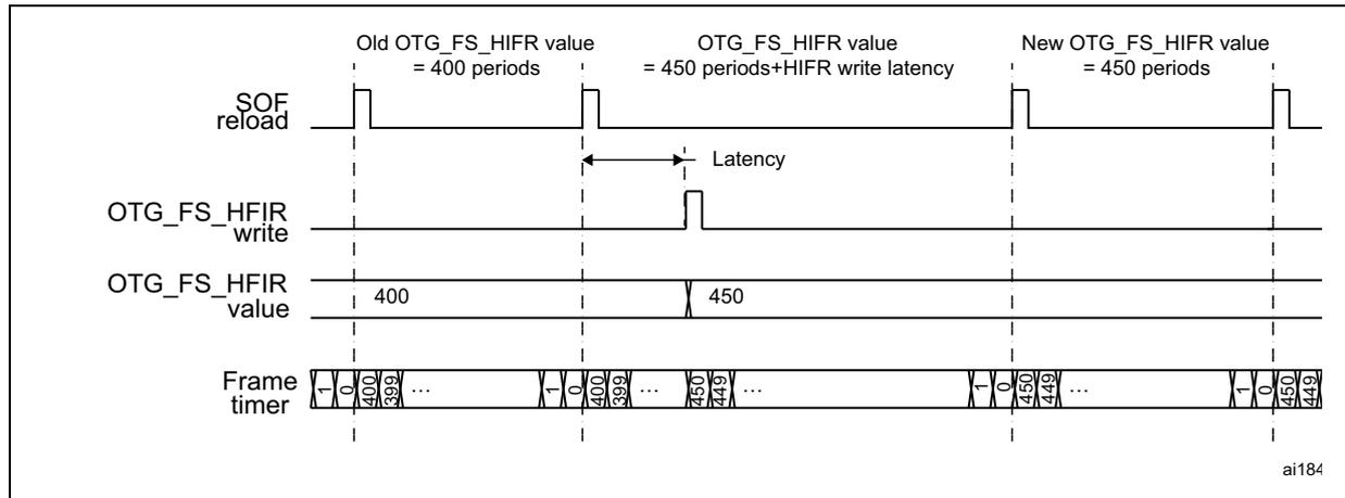
The diagram illustrates the timing for updating the OTG_FS_HFIR register dynamically. It consists of four horizontal timelines:
- SOF reload: Shows periodic pulses representing the start of each USB frame.
- OTG_FS_HFIR write: Shows a pulse indicating the time when the new value is written to the register.
- OTG_FS_HFIR value: Shows the current value of the register. It starts at 400 periods (Old OTG_FS_HFIR value) and changes to 450 periods (New OTG_FS_HFIR value) after the write. The value at the time of the write is labeled as 450 periods + HFIR write latency.
- Frame timer: Shows the progression of frames (0, 1, 2, 3, ...). The timer is reset by SOF reloads. The update of the HFIR value from 400 to 450 is shown occurring between frames.
Key timing points and labels:
- Old OTG_FS_HFIR value = 400 periods: The value before the update.
- OTG_FS_HFIR value = 450 periods + HFIR write latency: The value at the time of the write.
- New OTG_FS_HFIR value = 450 periods: The value after the update.
- Latency: The time interval between the SOF reload and the OTG_FS_HFIR write.
- ai184: A small identifier in the bottom right corner of the diagram.
22.10 USB data FIFOs
The USB system features 1.25 Kbyte of dedicated RAM with a sophisticated FIFO control mechanism. The packet FIFO controller module in the OTG_FS core organizes RAM space into Tx-FIFOs into which the application pushes the data to be temporarily stored before the USB transmission, and into a single Rx FIFO where the data received from the USB are temporarily stored before retrieval (popped) by the application. The number of instructed FIFOs and how these are organized inside the RAM depends on the device's role. In peripheral mode an additional Tx-FIFO is instructed for each active IN endpoint. Any FIFO size is software configured to better meet the application requirements.
22.11 Peripheral FIFO architecture
Figure 248. Device-mode FIFO address mapping and AHB FIFO access mapping
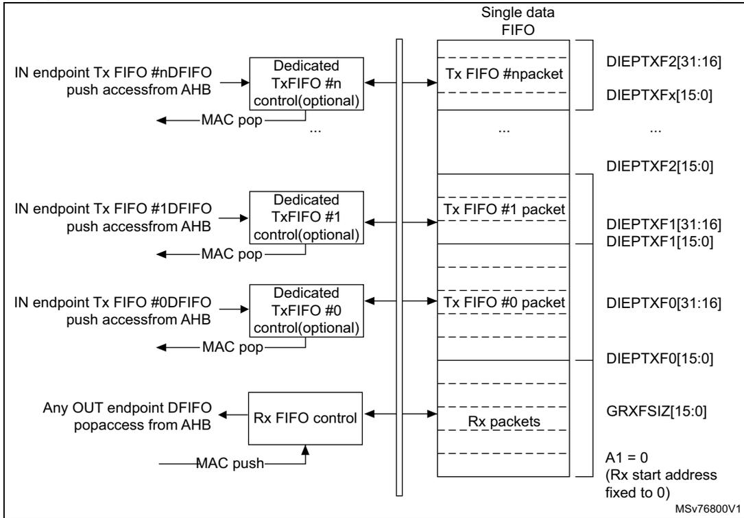
The diagram illustrates the device-mode FIFO architecture. On the left, four IN endpoint Tx FIFOs (#nDFIFO, #1DFIFO, #0DFIFO, and a generic OUT endpoint DFIFO) are shown. Each IN endpoint has a 'Dedicated TxFIFO #n control(optional)' block. AHB push access goes into these controls, and MAC pop access comes from them. The OUT endpoint DFIFO has an 'Rx FIFO control' block. AHB pop access goes into this control, and MAC push access comes from it. All these controls are connected to a central 'Single data FIFO'. Inside the 'Single data FIFO', there are sections for 'Tx FIFO #npacket', 'Tx FIFO #1 packet', 'Tx FIFO #0 packet', and 'Rx packets'. To the right of the FIFO, memory addresses are listed: DIEPTXF2[31:16], DIEPTXFx[15:0], ..., DIEPTXF2[15:0], DIEPTXF1[31:16], DIEPTXF1[15:0], ..., DIEPTXF0[31:16], DIEPTXF0[15:0], ..., GRXFSIZ[15:0], and A1 = 0 (Rx start address fixed to 0). The diagram is labeled MSV76800V1.
22.11.1 Peripheral Rx FIFO
The OTG peripheral uses a single receive FIFO that receives the data directed to all OUT endpoints. Received packets are stacked back-to-back until free space is available in the Rx-FIFO. The status of the received packet (which contains the OUT endpoint destination number, the byte count, the data PID and the validity of the received data) is also stored by the core on top of the data payload. When no more space is available, host transactions are NACKed and an interrupt is received on the addressed endpoint. The size of the receive FIFO is configured in the receive FIFO Size register (GRXFSIZ).
The single receive FIFO architecture makes it more efficient for the USB peripheral to fill in the receive RAM buffer:
- • All OUT endpoints share the same RAM buffer (shared FIFO)
- • The OTG FS core can fill in the receive FIFO up to the limit for any host sequence of OUT tokens
The application keeps receiving the Rx-FIFO non-empty interrupt (RXFLVL bit in OTG_FS_GINTSTS) as long as there is at least one packet available for download. It reads the packet information from the receive status read and pop register (GRXSTSP) and finally pops data off the receive FIFO by reading from the endpoint-related pop address.
22.11.2 Peripheral Tx FIFOs
The core has a dedicated FIFO for each IN endpoint. The application configures FIFO sizes by writing the non periodic transmit FIFO size register (OTG_FS_TX0FSIZ) for IN endpoint0 and the device IN endpoint transmit FIFOx registers (DIEPTXFx) for IN endpoint-x.
22.12 Host FIFO architecture
Figure 249. Host-mode FIFO address mapping and AHB FIFO access mapping
![Diagram of Host-mode FIFO architecture showing the mapping of AHB FIFO access to a single data FIFO. The diagram illustrates three types of FIFO control blocks: Periodic Tx FIFO control (optional), Non-periodic Tx FIFO control, and Rx FIFO control. These controls interface with a single data FIFO that contains Periodic Tx packets, Non-periodic Tx packets, and Rx packets. The Periodic Tx packets are associated with HPTXFSIZ[31:16] and HPTXFSIZ[15:0] registers. The Non-periodic Tx packets are associated with HNPTXFSIZ[31:16] and HNPTXFSIZ[15:0] registers. The Rx packets are associated with GRXFSIZ[15:0] and a fixed start address of 0 A1=0. The diagram also shows the flow of data from the AHB to the FIFO and from the FIFO to the MAC.](/RM0368-STM32F401xB-C-401xD-E/657407066133429a83c293477321520a_img.jpg)
The diagram illustrates the Host-mode FIFO architecture. On the left, three control blocks are shown: 'Periodic Tx FIFO control (optional)', 'Non-periodic Tx FIFO control', and 'Rx FIFO control'. The 'Periodic Tx FIFO control' is associated with 'Any periodic channel DFIFO push access from AHB' and 'MAC pop'. The 'Non-periodic Tx FIFO control' is associated with 'Any non-periodic channel DFIFO push access from AHB' and 'MAC pop'. The 'Rx FIFO control' is associated with 'Any channel DFIFO pop access from AHB' and 'MAC push'. These controls interface with a 'Single data FIFO' on the right. The 'Single data FIFO' contains 'Periodic Tx packets', 'Non-periodic Tx packets', and 'Rx packets'. The 'Periodic Tx packets' are associated with 'HPTXFSIZ[31:16]' and 'HPTXFSIZ[15:0]' registers. The 'Non-periodic Tx packets' are associated with 'HNPTXFSIZ[31:16]' and 'HNPTXFSIZ[15:0]' registers. The 'Rx packets' are associated with 'GRXFSIZ[15:0]' and 'Rx start address fixed to 0 A1=0'. The diagram also shows the flow of data from the AHB to the FIFO and from the FIFO to the MAC.
22.12.1 Host Rx FIFO
The host uses one receiver FIFO for all periodic and nonperiodic transactions. The FIFO is used as a receive buffer to hold the received data (payload of the received packet) from the USB until it is transferred to the system memory. Packets received from any remote IN endpoint are stacked back-to-back until free space is available. The status of each received packet with the host channel destination, byte count, data PID and validity of the received data are also stored into the FIFO. The size of the receive FIFO is configured in the receive FIFO size register (GRXFSIZ).
The single receive FIFO architecture makes it highly efficient for the USB host to fill in the receive data buffer:
- • All IN configured host channels share the same RAM buffer (shared FIFO)
- • The OTG_FS core can fill in the receive FIFO up to the limit for any sequence of IN tokens driven by the host software
The application receives the Rx FIFO not-empty interrupt as long as there is at least one packet available for download. It reads the packet information from the receive status read and pop register and finally pops the data off the receive FIFO.
22.12.2 Host Tx FIFOs
The host uses one transmit FIFO for all non-periodic (control and bulk) OUT transactions and one transmit FIFO for all periodic (isochronous and interrupt) OUT transactions. FIFOs are used as transmit buffers to hold the data (payload of the transmit packet) to be transmitted over the USB. The size of the periodic (nonperiodic) Tx FIFO is configured in the host periodic (nonperiodic) transmit FIFO size (HPTXFSIZ/HNPTXFSIZ) register.
The two Tx FIFO implementation derives from the higher priority granted to the periodic type of traffic over the USB frame. At the beginning of each frame, the built-in host scheduler processes the periodic request queue first, followed by the nonperiodic request queue.
The two transmit FIFO architecture provides the USB host with separate optimization for periodic and nonperiodic transmit data buffer management:
- • All host channels configured to support periodic (nonperiodic) transactions in the OUT direction share the same RAM buffer (shared FIFOs)
- • The OTG_FS core can fill in the periodic (nonperiodic) transmit FIFO up to the limit for any sequence of OUT tokens driven by the host software
The OTG_FS core issues the periodic Tx FIFO empty interrupt (PTXFE bit in OTG_FS_GINTSTS) as long as the periodic Tx-FIFO is half or completely empty, depending on the value of the periodic Tx-FIFO empty level bit in the AHB configuration register (PTXFELVL bit in OTG_FS_GAHBCFG). The application can push the transmission data in advance as long as free space is available in both the periodic Tx FIFO and the periodic request queue. The host periodic transmit FIFO and queue status register (HPTXSTS) can be read to know how much space is available in both.
OTG_FS core issues the non periodic Tx FIFO empty interrupt (NPTXFE bit in OTG_FS_GINTSTS) as long as the nonperiodic Tx FIFO is half or completely empty depending on the non periodic Tx FIFO empty level bit in the AHB configuration register (TXFELVL bit in OTG_FS_GAHBCFG). The application can push the transmission data as long as free space is available in both the nonperiodic Tx FIFO and nonperiodic request queue. The host nonperiodic transmit FIFO and queue status register (HNPTXSTS) can be read to know how much space is available in both.
22.13 FIFO RAM allocation
22.13.1 Device mode
Receive FIFO RAM allocation: the application should allocate RAM for SETUP Packets: 10 locations must be reserved in the receive FIFO to receive SETUP packets on control endpoint. The core does not use these locations, which are reserved for SETUP packets, to write any other data. One location is to be allocated for Global OUT NAK. Status information is written to the FIFO along with each received packet. Therefore, a minimum space of \( (\text{Largest Packet Size} / 4) + 1 \) must be allocated to receive packets. If multiple isochronous endpoints are enabled, then at least two \( (\text{Largest Packet Size} / 4) + 1 \) spaces must be allocated to receive back-to-back packets. Typically, two \( (\text{Largest Packet Size} / 4) + 1 \) spaces are recommended so that when the previous packet is being transferred to the CPU, the USB can receive the subsequent packet.
Along with the last packet for each endpoint, transfer complete status information is also pushed to the FIFO. Typically, one location for each OUT endpoint is recommended.
Transmit FIFO RAM allocation: the minimum RAM space required for each IN Endpoint Transmit FIFO is the maximum packet size for that particular IN endpoint.
Note: More space allocated in the transmit IN Endpoint FIFO results in better performance on the USB.
22.13.2 Host mode
Receive FIFO RAM allocation
Status information is written to the FIFO along with each received packet. Therefore, a minimum space of \( (\text{Largest Packet Size} / 4) + 1 \) must be allocated to receive packets. If multiple isochronous channels are enabled, then at least two \( (\text{Largest Packet Size} / 4) + 1 \) spaces must be allocated to receive back-to-back packets. Typically, two \( (\text{Largest Packet Size} / 4) + 1 \) spaces are recommended so that when the previous packet is being transferred to the CPU, the USB can receive the subsequent packet.
Along with the last packet in the host channel, transfer complete status information is also pushed to the FIFO. So one location must be allocated for this.
Transmit FIFO RAM allocation
The minimum amount of RAM required for the host Non-periodic Transmit FIFO is the largest maximum packet size among all supported non-periodic OUT channels.
Typically, two Largest Packet Sizes worth of space is recommended, so that when the current packet is under transfer to the USB, the CPU can get the next packet.
The minimum amount of RAM required for host periodic Transmit FIFO is the largest maximum packet size out of all the supported periodic OUT channels. If there is at least one Isochronous OUT endpoint, then the space must be at least two times the maximum packet size of that channel.
Note: More space allocated in the Transmit Non-periodic FIFO results in better performance on the USB.
22.14 USB system performance
Best USB and system performance is achieved owing to the large RAM buffers, the highly configurable FIFO sizes, the quick 32-bit FIFO access through AHB push/pop registers and, especially, the advanced FIFO control mechanism. Indeed, this mechanism allows the OTG_FS to fill in the available RAM space at best regardless of the current USB sequence. With these features:
- • The application gains good margins to calibrate its intervention in order to optimize the CPU bandwidth usage:
- – It can accumulate large amounts of transmission data in advance compared to when they are effectively sent over the USB
- – It benefits of a large time margin to download data from the single receive FIFO
- • The USB Core is able to maintain its full operating rate, that is to provide maximum full-speed bandwidth with a great margin of autonomy versus application intervention:
- – It has a large reserve of transmission data at its disposal to autonomously manage the sending of data over the USB
- – It has a lot of empty space available in the receive buffer to autonomously fill it in with the data coming from the USB
As the OTG_FS core is able to fill in the 1.25 Kbyte RAM buffer very efficiently, and as 1.25 Kbyte of transmit/receive data is more than enough to cover a full speed frame, the USB system is able to withstand the maximum full-speed data rate for up to one USB frame (1 ms) without any CPU intervention.
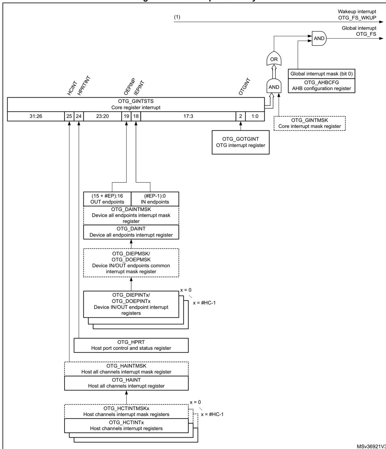
22.15 OTG_FS interrupts
When the OTG_FS controller is operating in one mode, either device or host, the application must not access registers from the other mode. If an illegal access occurs, a mode mismatch interrupt is generated and reflected in the Core interrupt register (MMIS bit in the OTG_FS_GINTSTS register). When the core switches from one mode to the other, the registers in the new mode of operation must be reprogrammed as they would be after a power-on reset.
Figure 250 shows the interrupt hierarchy.
Figure 250. Interrupt hierarchy
(1)
Wakeup interrupt
OTG_FS_WKUP
Global interrupt
OTG_FS
AND
OR
AND
Global interrupt mask (bit 0)
OTG_AHBCFG
AHB configuration register
HCINT
HPRTINT
OEPINT
IEPINT
OTGINT
Core register interrupt
| 31:26 | 25 | 24 | 23:20 | 19 | 18 | 17:3 | 2 | 1:0 |
Core interrupt mask register
OTG interrupt register
OUT endpoints
IN endpoints
Device all endpoints interrupt mask register
Device all endpoints interrupt register
OTG_DOEPMSK
Device IN/OUT endpoints common interrupt mask register
OTG_DOEPINTx
Device IN/OUT endpoint interrupt registers
x = 0
x = #HC-1
Host port control and status register
Host all channels interrupt mask register
Host all channels interrupt register
Host channels interrupt mask registers
Host channels interrupt registers
x = 0
x = #HC-1
MSv36921V3
- 1. OTG_FS_WKUP become active (high state) when resume condition occurs during L1 SLEEP or L2 SUSPEND states.
22.16 OTG_FS control and status registers
By reading from and writing to the control and status registers (CSRs) through the AHB slave interface, the application controls the OTG_FS controller. These registers are 32 bits wide, and the addresses are 32-bit block aligned. The OTG_FS registers must be accessed by words (32 bits).
CSRs are classified as follows:
- • Core global registers
- • Host-mode registers
- • Host global registers
- • Host port CSRs
- • Host channel-specific registers
- • Device-mode registers
- • Device global registers
- • Device endpoint-specific registers
- • Power and clock-gating registers
- • Data FIFO (DFIFO) access registers
Only the Core global, Power and clock-gating, Data FIFO access, and host port control and status registers can be accessed in both host and device modes. When the OTG_FS controller is operating in one mode, either device or host, the application must not access registers from the other mode. If an illegal access occurs, a mode mismatch interrupt is generated and reflected in the Core interrupt register (MMIS bit in the OTG_FS_GINTSTS register). When the core switches from one mode to the other, the registers in the new mode of operation must be reprogrammed as they would be after a power-on reset.
22.16.1 CSR memory map
The host and device mode registers occupy different addresses. All registers are implemented in the AHB clock domain.
Figure 251. CSR memory map
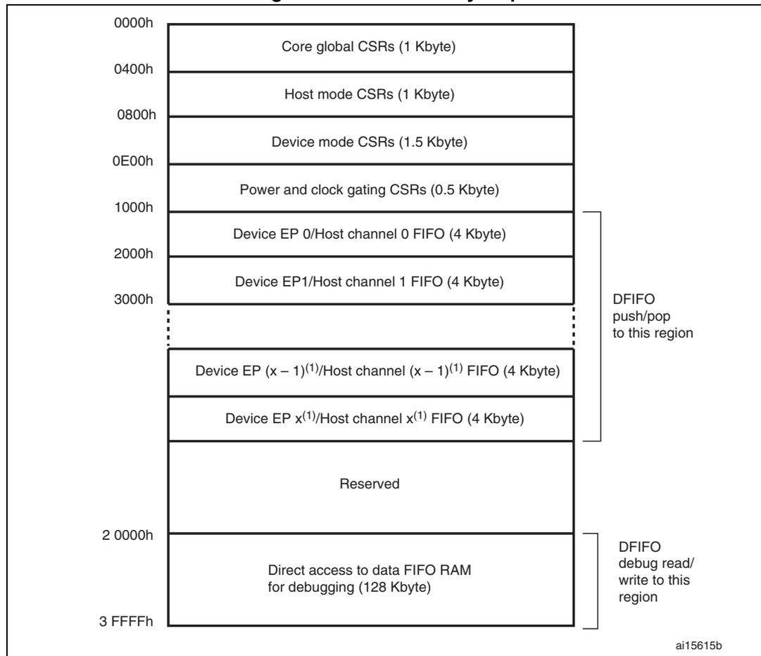
The diagram illustrates the CSR memory map with the following address ranges and contents:
- 0000h to 0400h: Core global CSRs (1 Kbyte)
- 0400h to 0800h: Host mode CSRs (1 Kbyte)
- 0800h to 0E00h: Device mode CSRs (1.5 Kbyte)
- 0E00h to 1000h: Power and clock gating CSRs (0.5 Kbyte)
- 1000h to 2000h: Device EP 0/Host channel 0 FIFO (4 Kbyte)
- 2000h to 3000h: Device EP1/Host channel 1 FIFO (4 Kbyte)
- 3000h to 20000h: Device EP (x - 1) (1) /Host channel (x - 1) (1) FIFO (4 Kbyte) and Device EP x (1) /Host channel x (1) FIFO (4 Kbyte). This region is labeled "DFIFO push/pop to this region".
- 20000h to 3FFFFh: Reserved and Direct access to data FIFO RAM for debugging (128 Kbyte). This region is labeled "DFIFO debug read/write to this region".
ai15615b
1. x = 3 in device mode and x = 7 in host mode.
Global CSR map
These registers are available in both host and device modes.
Table 128. Core global control and status registers (CSRs)
| Acronym | Address offset | Register name |
|---|---|---|
| OTG_FS_GOTGCTL | 0x000 | OTG_FS control and status register (OTG_FS_GOTGCTL) on page 700 |
| OTG_FS_GOTGINT | 0x004 | OTG_FS interrupt register (OTG_FS_GOTGINT) on page 701 |
| OTG_FS_GAHBCFG | 0x008 | OTG_FS AHB configuration register (OTG_FS_GAHBCFG) on page 703 |
| OTG_FS_GUSBCFG | 0x00C | OTG_FS USB configuration register (OTG_FS_GUSBCFG) on page 704 |
| OTG_FS_GRSTCTL | 0x010 | OTG_FS reset register (OTG_FS_GRSTCTL) on page 706 |
| Acronym | Address offset | Register name |
|---|---|---|
| OTG_FS_GINTSTS | 0x014 | OTG_FS core interrupt register (OTG_FS_GINTSTS) on page 708 |
| OTG_FS_GINTMSK | 0x018 | OTG_FS interrupt mask register (OTG_FS_GINTMSK) on page 712 |
| OTG_FS_GRXSTSR | 0x01C | OTG_FS Receive status debug read/OTG status read and pop registers (OTG_FS_GRXSTSR/OTG_FS_GRXSTSP) on page 715 |
| OTG_FS_GRXSTSP | 0x020 | |
| OTG_FS_GRXFSIZ | 0x024 | OTG_FS Receive FIFO size register (OTG_FS_GRXFSIZ) on page 716 |
| OTG_FS_HNPTXFSIZ/ OTG_FS_DIEPTXF0 (1) | 0x028 | OTG_FS Host non-periodic transmit FIFO size register (OTG_FS_HNPTXFSIZ)/Endpoint 0 Transmit FIFO size (OTG_FS_DIEPTXF0) |
| OTG_FS_HNPTXSTS | 0x02C | OTG_FS non-periodic transmit FIFO/queue status register (OTG_FS_HNPTXSTS) on page 717 |
| OTG_FS_GCCFG | 0x038 | OTG_FS general core configuration register (OTG_FS_GCCFG) on page 718 |
| OTG_FS_CID | 0x03C | OTG_FS core ID register (OTG_FS_CID) on page 719 |
| OTG_FS_HPTXFSIZ | 0x100 | OTG_FS Host periodic transmit FIFO size register (OTG_FS_HPTXFSIZ) on page 720 |
| OTG_FS_DIEPTXFx | 0x104 0x108 0x10C | OTG_FS device IN endpoint transmit FIFO size register (OTG_FS_DIEPTXFx) (x = 1..3, where x is the FIFO_number) on page 720 |
1. The general rule is to use OTG_FS_HNPTXFSIZ for host mode and OTG_FS_DIEPTXF0 for device mode.
Host-mode CSR map
These registers must be programmed every time the core changes to host mode.
Table 129. Host-mode control and status registers (CSRs)| Acronym | Offset address | Register name |
|---|---|---|
| OTG_FS_HCFG | 0x400 | OTG_FS Host configuration register (OTG_FS_HCFG) on page 721 |
| OTG_FS_HFIR | 0x404 | OTG_FS Host frame interval register (OTG_FS_HFIR) on page 721 |
| OTG_FS_HFNUM | 0x408 | OTG_FS Host frame number/frame time remaining register (OTG_FS_HFNUM) on page 722 |
| OTG_FS_HPTXSTS | 0x410 | OTG_FS Host periodic transmit FIFO/queue status register (OTG_FS_HPTXSTS) on page 722 |
| OTG_FS_HAINT | 0x414 | OTG_FS Host all channels interrupt register (OTG_FS_HAINT) on page 723 |
| OTG_FS_HAINTMSK | 0x418 | OTG_FS Host all channels interrupt mask register (OTG_FS_HAINTMSK) on page 724 |
| Acronym | Offset address | Register name |
|---|---|---|
| OTG_FS_HPRT | 0x440 | OTG_FS Host port control and status register (OTG_FS_HPRT) on page 724 |
| OTG_FS_HCCHARx | 0x500 0x520 ... 0x5E0 | OTG_FS Host channel-x characteristics register (OTG_FS_HCCHARx) (x = 0..7, where x = Channel_number) on page 727 |
| OTG_FS_HCINTx | 0x508 | OTG_FS Host channel-x interrupt register (OTG_FS_HCINTx) (x = 0..7, where x = Channel_number) on page 728 |
| OTG_FS_HCINTMSKx | 0x50C | OTG_FS Host channel-x interrupt mask register (OTG_FS_HCINTMSKx) (x = 0..7, where x = Channel_number) on page 729 |
| OTG_FS_HCTSIZx | 0x510 | OTG_FS Host channel-x transfer size register (OTG_FS_HCTSIZx) (x = 0..7, where x = Channel_number) on page 730 |
These registers must be programmed every time the core changes to device mode.
Table 130. Device-mode control and status registers| Acronym | Offset address | Register name |
|---|---|---|
| OTG_FS_DCFG | 0x800 | OTG_FS device configuration register (OTG_FS_DCFG) on page 731 |
| OTG_FS_DCTL | 0x804 | OTG_FS device control register (OTG_FS_DCTL) on page 732 |
| OTG_FS_DSTS | 0x808 | OTG_FS device status register (OTG_FS_DSTS) on page 733 |
| OTG_FS_DIEPMSK | 0x810 | OTG_FS device IN endpoint common interrupt mask register (OTG_FS_DIEPMSK) on page 734 |
| OTG_FS_DOEPMSK | 0x814 | OTG_FS device OUT endpoint common interrupt mask register (OTG_FS_DOEPMSK) on page 735 |
| OTG_FS_DAINT | 0x818 | OTG_FS device all endpoints interrupt register (OTG_FS_DAINT) on page 736 |
| OTG_FS_DAINTMSK | 0x81C | OTG_FS all endpoints interrupt mask register (OTG_FS_DAINTMSK) on page 737 |
| OTG_FS_DVBUSDIS | 0x828 | OTG_FS device V BUS discharge time register (OTG_FS_DVBUSDIS) on page 737 |
| OTG_FS_DVBUSPULSE | 0x82C | OTG_FS device V BUS pulsing time register (OTG_FS_DVBUSPULSE) on page 737 |
| OTG_FS_DIEPEPMSK | 0x834 | OTG_FS device IN endpoint FIFO empty interrupt mask register: (OTG_FS_DIEPEPMSK) on page 738 |
| OTG_FS_DIEPCTL0 | 0x900 | OTG_FS device control IN endpoint 0 control register (OTG_FS_DIEPCTL0) on page 738 |
Table 130. Device-mode control and status registers (continued)
| Acronym | Offset address | Register name |
|---|---|---|
| OTG_FS_DIEPCTLx | 0x920 0x940 0x960 | OTG device endpoint x control register (OTG_FS_DIEPCTLx) (x = 1..3, where x = Endpoint_number) on page 740 |
| OTG_FS_DIEPINTx | 0x908 | OTG_FS device endpoint-x interrupt register (OTG_FS_DIEPINTx) (x = 0..3, where x = Endpoint_number) on page 747 |
| OTG_FS_DIEPTSIZ0 | 0x910 | OTG_FS device IN endpoint 0 transfer size register (OTG_FS_DIEPTSIZ0) on page 749 |
| OTG_FS_DTXFSTSx | 0x918 | OTG_FS device IN endpoint transmit FIFO status register (OTG_FS_DTXFSTSx) (x = 0..3, where x = Endpoint_number) on page 753 |
| OTG_FS_DIEPTSIZx | 0x930 0x950 0x970 | OTG_FS device endpoint-x transfer size register (OTG_FS_DIEPTSIZx) (x = 1..3, where x = Endpoint_number) on page 752 |
| OTG_FS_DOEPCTL0 | 0xB00 | OTG_FS device control OUT endpoint 0 control register (OTG_FS_DOEPCTL0) on page 743 |
| OTG_FS_DOEPCTLx | 0xB20 0xB40 0xB60 | OTG device endpoint x control register (OTG_FS_DIEPCTLx) (x = 1..3, where x = Endpoint_number) on page 740 |
| OTG_FS_DOEPINTx | 0xB08 | OTG_FS device endpoint-x interrupt register (OTG_FS_DOEPINTx) (x = 0..3, where x = Endpoint_number) on page 748 |
| OTG_FS_DOPTSIZ0 | 0xB10 | OTG_FS device OUT endpoint 0 transfer size register (OTG_FS_DOPTSIZ0) on page 751 |
| OTG_FS_DOPTSIZx | 0xB30 0xB50 0xB70 | OTG_FS device OUT endpoint-x transfer size register (OTG_FS_DOPTSIZx) (x = 1..3, where x = Endpoint_number) on page 753 |
Data FIFO (DFIFO) access register map
These registers, available in both host and device modes, are used to read or write the FIFO space for a specific endpoint or a channel, in a given direction. If a host channel is of type IN, the FIFO can only be read on the channel. Similarly, if a host channel is of type OUT, the FIFO can only be written on the channel.
Table 131. Data FIFO (DFIFO) access register map
| FIFO access register section | Address range | Access |
|---|---|---|
| Device IN Endpoint 0/Host OUT Channel 0: DFIFO Write Access Device OUT Endpoint 0/Host IN Channel 0: DFIFO Read Access | 0x1000–0x1FFC | w r |
| Device IN Endpoint 1/Host OUT Channel 1: DFIFO Write Access Device OUT Endpoint 1/Host IN Channel 1: DFIFO Read Access | 0x2000–0x2FFC | w r |
| FIFO access register section | Address range | Access |
|---|---|---|
| ... | ... | ... |
| Device IN Endpoint x
(1)
/Host OUT Channel x
(1)
: DFIFO Write Access Device OUT Endpoint x (1) /Host IN Channel x (1) : DFIFO Read Access | 0xX000–0xXFFC | w r |
1. Where x is 3 in device mode and 7 in host mode.
Power and clock gating CSR map
There is a single register for power and clock gating. It is available in both host and device modes.
Table 132. Power and clock gating control and status registers| Register name | Acronym | Offset address: 0xE00–0xFFF |
|---|---|---|
| Power and clock gating control register | OTG_FS_PCGCTL | 0xE00-0xE04 |
| Reserved | - | 0xE05–0xFFF |
22.16.2 OTG_FS global registers
These registers are available in both host and device modes, and do not need to be reprogrammed when switching between these modes.
Bit values in the register descriptions are expressed in binary unless otherwise specified.
OTG_FS control and status register (OTG_FS_GOTGCTL)
Address offset: 0x000
Reset value: 0x0001 0000
The OTG_FS_GOTGCTL register controls the behavior and reflects the status of the OTG function of the core.
| 31 | 30 | 29 | 28 | 27 | 26 | 25 | 24 | 23 | 22 | 21 | 20 | 19 | 18 | 17 | 16 | 15 | 14 | 13 | 12 | 11 | 10 | 9 | 8 | 7 | 6 | 5 | 4 | 3 | 2 | 1 | 0 |
|---|---|---|---|---|---|---|---|---|---|---|---|---|---|---|---|---|---|---|---|---|---|---|---|---|---|---|---|---|---|---|---|
| Reserved | BSVLD | ASVLD | DBCT | CIDSTS | Reserved | DHNPEN | HSHNPEN | HNPRIQ | HNGSCS | Reserved | SRQ | SRQSCS | |||||||||||||||||||
| r | r | r | r | rw | rw | rw | r | rw | r | ||||||||||||||||||||||
Bits 31:20 Reserved, must be kept at reset value.
Bit 19 BSVLD : B-session valid
Indicates the device mode transceiver status.
0: B-session is not valid.
1: B-session is valid.
In OTG mode, you can use this bit to determine if the device is connected or disconnected.
Note: Only accessible in device mode.
Bit 18 ASVLD : A-session valid
Indicates the host mode transceiver status.
0: A-session is not valid
1: A-session is valid
Note: Only accessible in host mode.
Bit 17 DBCT : Long/short debounce time
Indicates the debounce time of a detected connection.
0: Long debounce time, used for physical connections (100 ms + 2.5 µs)
1: Short debounce time, used for soft connections (2.5 µs)
Note: Only accessible in host mode.
Bit 16 CIDSTS : Connector ID status
Indicates the connector ID status on a connect event.
0: The OTG_FS controller is in A-device mode
1: The OTG_FS controller is in B-device mode
Note: Accessible in both device and host modes.
Bits 15:12 Reserved, must be kept at reset value.
Bit 11 DHNPEN: Device HNP enabledThe application sets this bit when it successfully receives a SetFeature.SetHNPEnable command from the connected USB host.
0: HNP is not enabled in the application
1: HNP is enabled in the application
Note: Only accessible in device mode.
Bit 10 HSHNPEN: host set HNP enableThe application sets this bit when it has successfully enabled HNP (using the SetFeature.SetHNPEnable command) on the connected device.
0: Host Set HNP is not enabled
1: Host Set HNP is enabled
Note: Only accessible in host mode.
Bit 9 HNPRQ: HNP requestThe application sets this bit to initiate an HNP request to the connected USB host. The application can clear this bit by writing a 0 when the host negotiation success status change bit in the OTG_FS_GOTGINT register (HNSSCHG bit in OTG_FS_GOTGINT) is set. The core clears this bit when the HNSSCHG bit is cleared.
0: No HNP request
1: HNP request
Note: Only accessible in device mode.
Bit 8 HNGSCS: Host negotiation successThe core sets this bit when host negotiation is successful. The core clears this bit when the HNP Request (HNPRQ) bit in this register is set.
0: Host negotiation failure
1: Host negotiation success
Note: Only accessible in device mode.
Bits 7:2 Reserved, must be kept at reset value.
Bit 1 SRQ: Session requestThe application sets this bit to initiate a session request on the USB. The application can clear this bit by writing a 0 when the host negotiation success status change bit in the OTG_FS_GOTGINT register (HNSSCHG bit in OTG_FS_GOTGINT) is set. The core clears this bit when the HNSSCHG bit is cleared.
If you use the USB 1.1 full-speed serial transceiver interface to initiate the session request, the application must wait until \( V_{BUS} \) discharges to 0.2 V, after the B-Session Valid bit in this register (BSVLD bit in OTG_FS_GOTGCTL) is cleared.
0: No session request
1: Session request
Note: Only accessible in device mode.
Bit 0 SRQSCS: Session request successThe core sets this bit when a session request initiation is successful.
0: Session request failure
1: Session request success
Note: Only accessible in device mode.
OTG_FS interrupt register (OTG_FS_GOTGINT)Address offset: 0x04
Reset value: 0x0000 0000
The application reads this register whenever there is an OTG interrupt and clears the bits in this register to clear the OTG interrupt.
| 31 | 30 | 29 | 28 | 27 | 26 | 25 | 24 | 23 | 22 | 21 | 20 | 19 | 18 | 17 | 16 | 15 | 14 | 13 | 12 | 11 | 10 | 9 | 8 | 7 | 6 | 5 | 4 | 3 | 2 | 1 | 0 |
|---|---|---|---|---|---|---|---|---|---|---|---|---|---|---|---|---|---|---|---|---|---|---|---|---|---|---|---|---|---|---|---|
| Reserved | DBCDNE | ADTOCHG | HNGDET | Reserved | HNSSCHG | SRSSCHG | Reserved | SEDET | Res. | ||||||||||||||||||||||
Bits 31:20 Reserved, must be kept at reset value.
Bit 19 DBCDNE : Debounce done
The core sets this bit when the debounce is completed after the device connect. The application can start driving USB reset after seeing this interrupt. This bit is only valid when the HNP Capable or SRP Capable bit is set in the OTG_FS_GUSBCFG register (HNPCAP bit or SRPCAP bit in OTG_FS_GUSBCFG, respectively).
Note: Only accessible in host mode.
Bit 18 ADTOCHG : A-device timeout change
The core sets this bit to indicate that the A-device has timed out while waiting for the B-device to connect.
Note: Accessible in both device and host modes.
Bit 17 HNGDET : Host negotiation detected
The core sets this bit when it detects a host negotiation request on the USB.
Note: Accessible in both device and host modes.
Bits 16:10 Reserved, must be kept at reset value.
Bit 9 HNSSCHG : Host negotiation success status change
The core sets this bit on the success or failure of a USB host negotiation request. The application must read the host negotiation success bit of the OTG_FS_GOTGCTL register (HNGSCS in OTG_FS_GOTGCTL) to check for success or failure.
Note: Accessible in both device and host modes.
Bits 7:3 Reserved, must be kept at reset value.
Bit 8 SRSSCHG : Session request success status change
The core sets this bit on the success or failure of a session request. The application must read the session request success bit in the OTG_FS_GOTGCTL register (SRQSCS bit in OTG_FS_GOTGCTL) to check for success or failure.
Note: Accessible in both device and host modes.
Bit 2 SEDET : Session end detected
The core sets this bit to indicate that the level of the voltage on V BUS is no longer valid for a B-Peripheral session when V BUS < 0.8 V.
Bits 1:0 Reserved, must be kept at reset value.
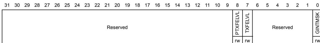
OTG_FS AHB configuration register (OTG_FS_GAHBCFG)
Address offset: 0x008
Reset value: 0x0000 0000
This register can be used to configure the core after power-on or a change in mode. This register mainly contains AHB system-related configuration parameters. Do not change this register after the initial programming. The application must program this register before starting any transactions on either the AHB or the USB.
| 31 | 30 | 29 | 28 | 27 | 26 | 25 | 24 | 23 | 22 | 21 | 20 | 19 | 18 | 17 | 16 | 15 | 14 | 13 | 12 | 11 | 10 | 9 | 8 | 7 | 6 | 5 | 4 | 3 | 2 | 1 | 0 |
| Reserved | PTXFELVL w | TXFELVL w | Reserved | GINTMSK w | |||||||||||||||||||||||||||
Bits 31:9 Reserved, must be kept at reset value.
Bit 8 PTXFELVL: Periodic TxFIFO empty level
Indicates when the periodic TxFIFO empty interrupt bit in the OTG_FS_GINTSTS register (PTXFE bit in OTG_FS_GINTSTS) is triggered.
- 0: PTXFE (in OTG_FS_GINTSTS) interrupt indicates that the Periodic TxFIFO is half empty
- 1: PTXFE (in OTG_FS_GINTSTS) interrupt indicates that the Periodic TxFIFO is completely empty
Note: Only accessible in host mode.
Bit 7 TXFELVL: TxFIFO empty level
In device mode, this bit indicates when IN endpoint Transmit FIFO empty interrupt (TXFE in OTG_FS_DIEPINTx.) is triggered.
- 0: the TXFE (in OTG_FS_DIEPINTx) interrupt indicates that the IN Endpoint TxFIFO is half empty
- 1: the TXFE (in OTG_FS_DIEPINTx) interrupt indicates that the IN Endpoint TxFIFO is completely empty
In host mode, this bit indicates when the nonperiodic Tx FIFO empty interrupt (NPTXFE bit in OTG_FS_GINTSTS) is triggered:
- 0: the NPTXFE (in OTG_FS_GINTSTS) interrupt indicates that the nonperiodic Tx FIFO is half empty
- 1: the NPTXFE (in OTG_FS_GINTSTS) interrupt indicates that the nonperiodic Tx FIFO is completely empty
Bits 6:1 Reserved, must be kept at reset value.
Bit 0 GINTMSK: Global interrupt mask
The application uses this bit to mask or unmask the interrupt line assertion to itself. Irrespective of this bit's setting, the interrupt status registers are updated by the core.
- 0: Mask the interrupt assertion to the application.
- 1: Unmask the interrupt assertion to the application.
Note: Accessible in both device and host modes.
OTG_FS USB configuration register (OTG_FS_GUSBCFG)
Address offset: 0x00C
Reset value: 0x0000 1440
This register can be used to configure the core after power-on or a changing to host mode or device mode. It contains USB and USB-PHY related configuration parameters. The application must program this register before starting any transactions on either the AHB or the USB. Do not make changes to this register after the initial programming.
| 31 | 30 | 29 | 28 | 27 | 26 | 25 | 24 | 23 | 22 | 21 | 20 | 19 | 18 | 17 | 16 | 15 | 14 | 13 | 12 | 11 | 10 | 9 | 8 | 7 | 6 | 5 | 4 | 3 | 2 | 1 | 0 |
|---|---|---|---|---|---|---|---|---|---|---|---|---|---|---|---|---|---|---|---|---|---|---|---|---|---|---|---|---|---|---|---|
| CTXPKT | FDMOD | FHMOD | Reserved | TRDT | HNPCA p | SRPCAP | Res. | PHYSEL | Reserved | TOCAL | |||||||||||||||||||||
| rw | rw | rw | rw | rw | rw | r | |||||||||||||||||||||||||
Bit 31 CTXPKT: Corrupt Tx packet
This bit is for debug purposes only. Never set this bit to 1.
Note: Accessible in both device and host modes.
Bit 30 FDMOD: Force device mode
Writing a 1 to this bit forces the core to device mode irrespective of the OTG_FS_ID input pin.
0: Normal mode
1: Force device mode
After setting the force bit, the application must wait at least 25 ms before the change takes effect.
Note: Accessible in both device and host modes.
Bit 29 FHMOD: Force host mode
Writing a 1 to this bit forces the core to host mode irrespective of the OTG_FS_ID input pin.
0: Normal mode
1: Force host mode
After setting the force bit, the application must wait at least 25 ms before the change takes effect.
Note: Accessible in both device and host modes.
Bits 28:14 Reserved, must be kept at reset value.
Bits 13:10 TRDT: USB turnaround time
These bits allow setting the turnaround time in PHY clocks. They must be configured according to Table 133: TRDT values , depending on the application AHB frequency. Higher TRDT values allow stretching the USB response time to IN tokens in order to compensate for longer AHB read access latency to the Data FIFO.
Note: Only accessible in device mode.
Bit 9 HNPCAP: HNP-capable
The application uses this bit to control the OTG_FS controller's HNP capabilities.
0: HNP capability is not enabled.
1: HNP capability is enabled.
Note: Accessible in both device and host modes.
Bit 8 SRPCAP : SRP-capable
The application uses this bit to control the OTG_FS controller's SRP capabilities. If the core operates as a non-SRP-capable
B-device, it cannot request the connected A-device (host) to activate V BUS and start a session.
0: SRP capability is not enabled.
1: SRP capability is enabled.
Note: Accessible in both device and host modes.
Bit 7 Reserved, must be kept at reset value.
Bit 6 PHYSEL : Full speed serial transceiver select
This bit is always 1 with read-only access.
Bits 5:3 Reserved, must be kept at reset value.
Bits 2:0 TOCAL : FS timeout calibration
The number of PHY clocks that the application programs in this field is added to the full-speed interpacket timeout duration in the core to account for any additional delays introduced by the PHY. This can be required, because the delay introduced by the PHY in generating the line state condition can vary from one PHY to another.
The USB standard timeout value for full-speed operation is 16 to 18 (inclusive) bit times. The application must program this field based on the speed of enumeration. The number of bit times added per PHY clock is 0.25 bit times.
Table 133. TRDT values
| AHB frequency range (MHz) | TRDT minimum value | |
|---|---|---|
| Min. | Max | |
| 14.2 | 15 | 0xF |
| 15 | 16 | 0xE |
| 16 | 17.2 | 0xD |
| 17.2 | 18.5 | 0xC |
| 18.5 | 20 | 0xB |
| 20 | 21.8 | 0xA |
| 21.8 | 24 | 0x9 |
| 24 | 27.5 | 0x8 |
| 27.5 | 32 | 0x7 |
| 32 | - | 0x6 |
Address offset: 0x010
Reset value: 0x8000 0000
The application uses this register to reset various hardware features inside the core.
| 31 | 30 | 29 | 28 | 27 | 26 | 25 | 24 | 23 | 22 | 21 | 20 | 19 | 18 | 17 | 16 | 15 | 14 | 13 | 12 | 11 | 10 | 9 | 8 | 7 | 6 | 5 | 4 | 3 | 2 | 1 | 0 | |
| AHBIDL | Reserved | TXFNUM | TXFFLSH | RXFFLSH | Reserved | FCRST | HSRST | CSRST | ||||||||||||||||||||||||
| r | rw | rs | rs | rs | rs | rs | ||||||||||||||||||||||||||
Bit 31 AHBIDL : AHB master idle
Indicates that the AHB master state machine is in the Idle condition.
Note: Accessible in both device and host modes.
Bits 30:11 Reserved, must be kept at reset value.
Bits 10:6 TXFNUM : TxFIFO number
This is the FIFO number that must be flushed using the TxFIFO Flush bit. This field must not be changed until the core clears the TxFIFO Flush bit.
00000:
- – Non-periodic TxFIFO flush in host mode
- – Tx FIFO 0 flush in device mode
00001:
- – Periodic TxFIFO flush in host mode
- – TXFIFO 1 flush in device mode
00010: TXFIFO 2 flush in device mode
...
00101: TXFIFO 15 flush in device mode
10000: Flush all the transmit FIFOs in device or host mode.
Note: Accessible in both device and host modes.
Bit 5 TXFFLSH : TxFIFO flush
This bit selectively flushes a single or all transmit FIFOs, but cannot do so if the core is in the midst of a transaction.
The application must write this bit only after checking that the core is neither writing to the TxFIFO nor reading from the TxFIFO. Verify using these registers:
Read—NAK Effective Interrupt ensures the core is not reading from the FIFO
Write—AHBIDL bit in OTG_FS_GRSTCTL ensures the core is not writing anything to the FIFO.
Note: Accessible in both device and host modes.
Bit 4 RXFFLSH : RxFIFO flush
The application can flush the entire RxFIFO using this bit, but must first ensure that the core is not in the middle of a transaction.
The application must only write to this bit after checking that the core is neither reading from the RxFIFO nor writing to the RxFIFO.
The application must wait until the bit is cleared before performing any other operations. This bit requires 8 clocks (slowest of PHY or AHB clock) to clear.
Note: Accessible in both device and host modes.
Bit 3 Reserved, must be kept at reset value.
Bit 2 FCRST: Host frame counter resetThe application writes this bit to reset the frame number counter inside the core. When the frame counter is reset, the subsequent SOF sent out by the core has a frame number of 0.
Note: Only accessible in host mode.
Bit 1 HSRST: HCLK soft resetThe application uses this bit to flush the control logic in the AHB Clock domain. Only AHB Clock Domain pipelines are reset.
FIFOs are not flushed with this bit.
All state machines in the AHB clock domain are reset to the Idle state after terminating the transactions on the AHB, following the protocol.
CSR control bits used by the AHB clock domain state machines are cleared.
To clear this interrupt, status mask bits that control the interrupt status and are generated by the AHB clock domain state machine are cleared.
Because interrupt status bits are not cleared, the application can get the status of any core events that occurred after it set this bit.
This is a self-clearing bit that the core clears after all necessary logic is reset in the core. This can take several clocks, depending on the core's current state.
Note: Accessible in both device and host modes.
Bit 0 CSRST: Core soft resetResets the HCLK and PCLK domains as follows:
Clears the interrupts and all the CSR register bits except for the following bits:
- – RSTPDMODL bit in OTG_FS_PCGCCTL
- – GAYEHCLK bit in OTG_FS_PCGCCTL
- – PWRCLMP bit in OTG_FS_PCGCCTL
- – STPPCLK bit in OTG_FS_PCGCCTL
- – FSLSPCS bit in OTG_FS_HCFG
- – DSPD bit in OTG_FS_DCFG
All module state machines (except for the AHB slave unit) are reset to the Idle state, and all the transmit FIFOs and the receive FIFO are flushed.
Any transactions on the AHB Master are terminated as soon as possible, after completing the last data phase of an AHB transfer. Any transactions on the USB are terminated immediately.
The application can write to this bit any time it wants to reset the core. This is a self-clearing bit and the core clears this bit after all the necessary logic is reset in the core, which can take several clocks, depending on the current state of the core. Once this bit has been cleared, the software must wait at least 3 PHY clocks before accessing the PHY domain (synchronization delay). The software must also check that bit 31 in this register is set to 1 (AHB Master is Idle) before starting any operation.
Typically, the software reset is used during software development and also when you dynamically change the PHY selection bits in the above listed USB configuration registers. When you change the PHY, the corresponding clock for the PHY is selected and used in the PHY domain. Once a new clock is selected, the PHY domain has to be reset for proper operation.
Note: Accessible in both device and host modes.
OTG_FS core interrupt register (OTG_FS_GINTSTS)
Address offset: 0x014
Reset value: 0x0400 0020
This register interrupts the application for system-level events in the current mode (device mode or host mode).
Some of the bits in this register are valid only in host mode, while others are valid in device mode only. This register also indicates the current mode. To clear the interrupt status bits of the rc_w1 type, the application must write 1 into the bit.
The FIFO status interrupts are read-only; once software reads from or writes to the FIFO while servicing these interrupts, FIFO interrupt conditions are cleared automatically.
The application must clear the OTG_FS_GINTSTS register at initialization before unmasking the interrupt bit to avoid any interrupts generated prior to initialization.
| 31 | 30 | 29 | 28 | 27 | 26 | 25 | 24 | 23 | 22 | 21 | 20 | 19 | 18 | 17 | 16 | 15 | 14 | 13 | 12 | 11 | 10 | 9 | 8 | 7 | 6 | 5 | 4 | 3 | 2 | 1 | 0 | |||||||||||||||
|---|---|---|---|---|---|---|---|---|---|---|---|---|---|---|---|---|---|---|---|---|---|---|---|---|---|---|---|---|---|---|---|---|---|---|---|---|---|---|---|---|---|---|---|---|---|---|
| WKUPINT | SRQINT | DISCINT | CIDSCHG | Reserved | PTXFE | HCINT | HPRTINT | Reserved | Reserved | IPXFR/INCOMPISOUT | ISOXFR | OEPINT | IEPINT | Reserved | EOFP | ISOODRP | ENUMDNE | USERST | USBSUSP | ESUSP | ||||||||||||||||||||||||||
| rc_w1 | r | r | r | Res. | rc_w1 | rc_w1 | r | r | r | r | rc_w1 | r | rc_w1 | r | GONAKEFF | GINAKEFF | NPTXFE | RXFLVL | SOF | OTGINT | MMIS | CMOD | ||||||||||||||||||||||||
Bit 31 WKUPINT : Resume/remote wake-up detected interrupt
In device mode, this interrupt is asserted when a resume is detected on the USB. In host mode, this interrupt is asserted when a remote wake-up is detected on the USB.
Note: Accessible in both device and host modes.
Bit 30 SRQINT : Session request/new session detected interrupt
In host mode, this interrupt is asserted when a session request is detected from the device. In device mode, this interrupt is asserted when V BUS is in the valid range for a B-peripheral device. Accessible in both device and host modes.
Bit 29 DISCINT : Disconnect detected interrupt
Asserted when a device disconnect is detected.
Note: Only accessible in host mode.
Bit 28 CIDSCHG : Connector ID status change
The core sets this bit when there is a change in connector ID status.
Note: Accessible in both device and host modes.
Bit 27 Reserved, must be kept at reset value.
Bit 26 PTXFE : Periodic TxFIFO empty
Asserted when the periodic transmit FIFO is either half or completely empty and there is space for at least one entry to be written in the periodic request queue. The half or completely empty status is determined by the periodic TxFIFO empty level bit in the OTG_FS_GAHBCFG register (PTXFELVL bit in OTG_FS_GAHBCFG).
Note: Only accessible in host mode.
Bit 25 HCINT: Host channels interruptThe core sets this bit to indicate that an interrupt is pending on one of the channels of the core (in host mode). The application must read the OTG_FS_HAINT register to determine the exact number of the channel on which the interrupt occurred, and then read the corresponding OTG_FS_HCINTx register to determine the exact cause of the interrupt. The application must clear the appropriate status bit in the OTG_FS_HCINTx register to clear this bit.
Note: Only accessible in host mode.
Bit 24 HPRTINT: Host port interruptThe core sets this bit to indicate a change in port status of one of the OTG_FS controller ports in host mode. The application must read the OTG_FS_HPRT register to determine the exact event that caused this interrupt. The application must clear the appropriate status bit in the OTG_FS_HPRT register to clear this bit.
Note: Only accessible in host mode.
Bits 23:22 Reserved, must be kept at reset value.
Bit 21 IPXFR: Incomplete periodic transferIn host mode, the core sets this interrupt bit when there are incomplete periodic transactions still pending, which are scheduled for the current frame.
INCOMPISOOUT: Incomplete isochronous OUT transferIn device mode, the core sets this interrupt to indicate that there is at least one isochronous OUT endpoint on which the transfer is not completed in the current frame. This interrupt is asserted along with the End of periodic frame interrupt (EOPF) bit in this register.
Bit 20 IISOIXFR: Incomplete isochronous IN transferThe core sets this interrupt to indicate that there is at least one isochronous IN endpoint on which the transfer is not completed in the current frame. This interrupt is asserted along with the End of periodic frame interrupt (EOPF) bit in this register.
Note: Only accessible in device mode.
Bit 19 OEPINT: OUT endpoint interruptThe core sets this bit to indicate that an interrupt is pending on one of the OUT endpoints of the core (in device mode). The application must read the OTG_FS_DAINT register to determine the exact number of the OUT endpoint on which the interrupt occurred, and then read the corresponding OTG_FS_DOEPINTx register to determine the exact cause of the interrupt. The application must clear the appropriate status bit in the corresponding OTG_FS_DOEPINTx register to clear this bit.
Note: Only accessible in device mode.
Bit 18 IEPINT: IN endpoint interruptThe core sets this bit to indicate that an interrupt is pending on one of the IN endpoints of the core (in device mode). The application must read the OTG_FS_DAINT register to determine the exact number of the IN endpoint on which the interrupt occurred, and then read the corresponding OTG_FS_DIEPINTx register to determine the exact cause of the interrupt.
The application must clear the appropriate status bit in the corresponding OTG_FS_DIEPINTx register to clear this bit.
Note: Only accessible in device mode.
Bits 17:16 Reserved, must be kept at reset value.
Bit 15 EOPF: End of periodic frame interruptIndicates that the period specified in the periodic frame interval field of the OTG_FS_DCFG register (PFIVL bit in OTG_FS_DCFG) has been reached in the current frame.
Note: Only accessible in device mode.
Bit 14 ISOODRP: Isochronous OUT packet dropped interruptThe core sets this bit when it fails to write an isochronous OUT packet into the RxFIFO because the RxFIFO does not have enough space to accommodate a maximum size packet for the isochronous OUT endpoint.
Note: Only accessible in device mode.
Bit 13 ENUMDNE: Enumeration doneThe core sets this bit to indicate that speed enumeration is complete. The application must read the OTG_FS_DSTS register to obtain the enumerated speed.
Note: Only accessible in device mode.
Bit 12 USBRST: USB resetThe core sets this bit to indicate that a reset is detected on the USB.
Note: Only accessible in device mode.
Bit 11 USBSUSP: USB suspendThe core sets this bit to indicate that a suspend was detected on the USB. The core enters the Suspended state when there is no activity on the data lines for a period of 3 ms.
Note: Only accessible in device mode.
Bit 10 ESUSP: Early suspendThe core sets this bit to indicate that an Idle state has been detected on the USB for 3 ms.
Note: Only accessible in device mode.
Bits 9:8 Reserved, must be kept at reset value.
Bit 7 GONAKEFF: Global OUT NAK effectiveIndicates that the Set global OUT NAK bit in the OTG_FS_DCTL register (SGONAK bit in OTG_FS_DCTL), set by the application, has taken effect in the core. This bit can be cleared by writing the Clear global OUT NAK bit in the OTG_FS_DCTL register (CGONAK bit in OTG_FS_DCTL).
Note: Only accessible in device mode.
Bit 6 GINAKEFF: Global IN non-periodic NAK effectiveIndicates that the Set global non-periodic IN NAK bit in the OTG_FS_DCTL register (SGINAK bit in OTG_FS_DCTL), set by the application, has taken effect in the core. That is, the core has sampled the Global IN NAK bit set by the application. This bit can be cleared by clearing the Clear global non-periodic IN NAK bit in the OTG_FS_DCTL register (CGINAK bit in OTG_FS_DCTL).
This interrupt does not necessarily mean that a NAK handshake is sent out on the USB. The STALL bit takes precedence over the NAK bit.
Note: Only accessible in device mode.
Bit 5 NPTXFE: Non-periodic TxFIFO emptyThis interrupt is asserted when the non-periodic TxFIFO is either half or completely empty, and there is space for at least one entry to be written to the non-periodic transmit request queue. The half or completely empty status is determined by the non-periodic TxFIFO empty level bit in the OTG_FS_GAHBCFG register (TXFELVL bit in OTG_FS_GAHBCFG).
Note: Accessible in host mode only.
Bit 4 RXFLVL: RxFIFO non-emptyIndicates that there is at least one packet pending to be read from the RxFIFO.
Note: Accessible in both host and device modes.
Bit 3 SOF: Start of frameIn host mode, the core sets this bit to indicate that an SOF (FS), or Keep-Alive (LS) is transmitted on the USB. The application must write a 1 to this bit to clear the interrupt.
In device mode, in the core sets this bit to indicate that an SOF token has been received on the USB. The application can read the Device Status register to get the current frame number. This interrupt is seen only when the core is operating in FS.
Note: Accessible in both host and device modes.
Bit 2 OTGINT: OTG interruptThe core sets this bit to indicate an OTG protocol event. The application must read the OTG Interrupt Status (OTG_FS_GOTGINT) register to determine the exact event that caused this interrupt. The application must clear the appropriate status bit in the OTG_FS_GOTGINT register to clear this bit.
Note: Accessible in both host and device modes.
Bit 1 MMIS: Mode mismatch interruptThe core sets this bit when the application is trying to access:
- – A host mode register, when the core is operating in device mode
- – A device mode register, when the core is operating in host mode
The register access is completed on the AHB with an OKAY response, but is ignored by the core internally and does not affect the operation of the core.
Note: Accessible in both host and device modes.
Bit 0 CMOD: Current mode of operationIndicates the current mode.
0: Device mode
1: Host mode
Note: Accessible in both host and device modes.
OTG_FS interrupt mask register (OTG_FS_GINTMSK)
Address offset: 0x018
Reset value: 0x0000 0000
This register works with the Core interrupt register to interrupt the application. When an interrupt bit is masked, the interrupt associated with that bit is not generated. However, the Core Interrupt (OTG_FS_GINTSTS) register bit corresponding to that interrupt is still set.
| 31 | 30 | 29 | 28 | 27 | 26 | 25 | 24 | 23 | 22 | 21 | 20 | 19 | 18 | 17 | 16 | 15 | 14 | 13 | 12 | 11 | 10 | 9 | 8 | 7 | 6 | 5 | 4 | 3 | 2 | 1 | 0 |
|---|---|---|---|---|---|---|---|---|---|---|---|---|---|---|---|---|---|---|---|---|---|---|---|---|---|---|---|---|---|---|---|
| WUIM | SRQIM | DISCINT | CID SCHGM | Reserved | PTXFEM | HCIM | PRTIM | Reserved | IPXFRM/ISOOXFRM | IISOXFRM | OEPINT | IEPINT | Reserved | EOPEM | ISOODRPM | ENUMDNEM | USBRST | USBSUSPM | ESUSPM | Reserved | GONAKEFFM | GINAKEFFM | NPTXFEM | PXFLVLM | SOFM | OTGINT | MMISM | Reserved | |||
| rw | rw | rw | rw | rw | rw | rw | rw | rw | rw | rw | rw | rw | rw | rw | rw | rw | rw | rw | rw | rw | rw | rw | rw | rw | rw | rw |
Bit 31 WUIM : Resume/remote wake-up detected interrupt mask
0: Masked interrupt
1: Unmasked interrupt
Note: Accessible in both host and device modes.
Bit 30 SRQIM : Session request/new session detected interrupt mask
0: Masked interrupt
1: Unmasked interrupt
Note: Accessible in both host and device modes.
Bit 29 DISCINT : Disconnect detected interrupt mask
0: Masked interrupt
1: Unmasked interrupt
Note: Only accessible in device mode.
Bit 28 CID SCHGM : Connector ID status change mask
0: Masked interrupt
1: Unmasked interrupt
Note: Accessible in both host and device modes.
Bit 27 Reserved, must be kept at reset value.
Bit 26 PTXFEM : Periodic TxFIFO empty mask
0: Masked interrupt
1: Unmasked interrupt
Note: Only accessible in host mode.
Bit 25 HCIM : Host channels interrupt mask
0: Masked interrupt
1: Unmasked interrupt
Note: Only accessible in host mode.
Bit 24 PRTIM : Host port interrupt mask
0: Masked interrupt
1: Unmasked interrupt
Note: Only accessible in host mode.
Bits 23:22 Reserved, must be kept at reset value.
Bit 21 IPXFRM : Incomplete periodic transfer mask
0: Masked interrupt
1: Unmasked interrupt
Note: Only accessible in host mode.
IISOOXFRM : Incomplete isochronous OUT transfer mask
0: Masked interrupt
1: Unmasked interrupt
Note: Only accessible in device mode.
Bit 20 IISOIXFRM : Incomplete isochronous IN transfer mask
0: Masked interrupt
1: Unmasked interrupt
Note: Only accessible in device mode.
Bit 19 OEPINT : OUT endpoints interrupt mask
0: Masked interrupt
1: Unmasked interrupt
Note: Only accessible in device mode.
Bit 18 IEPINT : IN endpoints interrupt mask
0: Masked interrupt
1: Unmasked interrupt
Note: Only accessible in device mode.
Bits 17:16 Reserved, must be kept at reset value.
Bit 15 EOPFM : End of periodic frame interrupt mask
0: Masked interrupt
1: Unmasked interrupt
Note: Only accessible in device mode.
Bit 14 ISOODRPM : Isochronous OUT packet dropped interrupt mask
0: Masked interrupt
1: Unmasked interrupt
Note: Only accessible in device mode.
Bit 13 ENUMDNEM : Enumeration done mask
0: Masked interrupt
1: Unmasked interrupt
Note: Only accessible in device mode.
Bit 12 USBRST : USB reset mask
0: Masked interrupt
1: Unmasked interrupt
Note: Only accessible in device mode.
Bit 11 USBSUSPM : USB suspend mask
0: Masked interrupt
1: Unmasked interrupt
Note: Only accessible in device mode.
Bit 10 ESUSPM : Early suspend mask
0: Masked interrupt
1: Unmasked interrupt
Note: Only accessible in device mode.
Bits 9:8 Reserved, must be kept at reset value.
Bit 7 GONAKEFFM : Global OUT NAK effective mask
0: Masked interrupt
1: Unmasked interrupt
Note: Only accessible in device mode.
Bit 6 GINAKEFFM : Global non-periodic IN NAK effective mask
0: Masked interrupt
1: Unmasked interrupt
Note: Only accessible in device mode.
Bit 5 NPTXFEM : Non-periodic TxFIFO empty mask
0: Masked interrupt
1: Unmasked interrupt
Note: Only accessible in Host mode.
Bit 4 RXFLVLM : Receive FIFO non-empty mask
0: Masked interrupt
1: Unmasked interrupt
Note: Accessible in both device and host modes.
Bit 3 SOFM : Start of frame mask
0: Masked interrupt
1: Unmasked interrupt
Note: Accessible in both device and host modes.
Bit 2 OTGINT : OTG interrupt mask
0: Masked interrupt
1: Unmasked interrupt
Note: Accessible in both device and host modes.
Bit 1 MMISM : Mode mismatch interrupt mask
0: Masked interrupt
1: Unmasked interrupt
Note: Accessible in both device and host modes.
Bit 0 Reserved, must be kept at reset value.
OTG_FS Receive status debug read/OTG status read and pop registers
(OTG_FS_GRXSTSR/OTG_FS_GRXSTSP)
Address offset for Read: 0x01C
Address offset for Pop: 0x020
Reset value: 0x0000 0000
A read to the Receive status debug read register returns the contents of the top of the Receive FIFO. A read to the Receive status read and pop register additionally pops the top data entry out of the RxFIFO.
The receive status contents must be interpreted differently in host and device modes. The core ignores the receive status pop/read when the receive FIFO is empty and returns a value of 0x0000 0000. The application must only pop the Receive Status FIFO when the Receive FIFO non-empty bit of the Core interrupt register (RXFLVL bit in OTG_FS_GINTSTS) is asserted.
Host mode
| 31 | 30 | 29 | 28 | 27 | 26 | 25 | 24 | 23 | 22 | 21 | 20 | 19 | 18 | 17 | 16 | 15 | 14 | 13 | 12 | 11 | 10 | 9 | 8 | 7 | 6 | 5 | 4 | 3 | 2 | 1 | 0 |
|---|---|---|---|---|---|---|---|---|---|---|---|---|---|---|---|---|---|---|---|---|---|---|---|---|---|---|---|---|---|---|---|
| Reserved | PKTSTS | DPID | BCNT | CHNUM | |||||||||||||||||||||||||||
| r | r | r | r | ||||||||||||||||||||||||||||
Bits 31:21 Reserved, must be kept at reset value.
Bits 20:17 PKTSTS : Packet status
Indicates the status of the received packet
0010: IN data packet received
0011: IN transfer completed (triggers an interrupt)
0101: Data toggle error (triggers an interrupt)
0111: Channel halted (triggers an interrupt)
Others: Reserved
Bits 16:15 DPID : Data PID
Indicates the Data PID of the received packet
00: DATA0
10: DATA1
01: DATA2
11: MDATA
Bits 14:4 BCNT : Byte count
Indicates the byte count of the received IN data packet.
Bits 3:0 CHNUM : Channel number
Indicates the channel number to which the current received packet belongs.
Device mode
| 31 | 30 | 29 | 28 | 27 | 26 | 25 | 24 | 23 | 22 | 21 | 20 | 19 | 18 | 17 | 16 | 15 | 14 | 13 | 12 | 11 | 10 | 9 | 8 | 7 | 6 | 5 | 4 | 3 | 2 | 1 | 0 |
|---|---|---|---|---|---|---|---|---|---|---|---|---|---|---|---|---|---|---|---|---|---|---|---|---|---|---|---|---|---|---|---|
| Reserved | FRMNUM | PKTSTS | DPID | BCNT | EPNUM | ||||||||||||||||||||||||||
| r | r | r | r | r | |||||||||||||||||||||||||||
Bits 31:25 Reserved, must be kept at reset value.
Bits 24:21 FRMNUM : Frame number
This is the least significant 4 bits of the frame number in which the packet is received on the USB. This field is supported only when isochronous OUT endpoints are supported.
Bits 20:17 PKTSTS : Packet status
Indicates the status of the received packet
0001: Global OUT NAK (triggers an interrupt)
0010: OUT data packet received
0011: OUT transfer completed (triggers an interrupt)
0100: SETUP transaction completed (triggers an interrupt)
0110: SETUP data packet received
Others: Reserved
Bits 16:15 DPID : Data PID
Indicates the Data PID of the received OUT data packet
00: DATA0
10: DATA1
01: DATA2
11: MDATA
Bits 14:4 BCNT : Byte count
Indicates the byte count of the received data packet.
Bits 3:0 EPNUM : Endpoint number
Indicates the endpoint number to which the current received packet belongs.
OTG_FS Receive FIFO size register (OTG_FS_GRXFSIZ)
Address offset: 0x024
Reset value: 0x0000 0200
The application can program the RAM size that must be allocated to the RxFIFO.
| 31 | 30 | 29 | 28 | 27 | 26 | 25 | 24 | 23 | 22 | 21 | 20 | 19 | 18 | 17 | 16 | 15 | 14 | 13 | 12 | 11 | 10 | 9 | 8 | 7 | 6 | 5 | 4 | 3 | 2 | 1 | 0 |
|---|---|---|---|---|---|---|---|---|---|---|---|---|---|---|---|---|---|---|---|---|---|---|---|---|---|---|---|---|---|---|---|
| Reserved | RXFD | ||||||||||||||||||||||||||||||
| rw | |||||||||||||||||||||||||||||||
Bits 31:16 Reserved, must be kept at reset value.
Bits 15:0 RXFD : RxFIFO depth
This value is in terms of 32-bit words.
Minimum value is 16
Maximum value is 256
The power-on reset value of this register is specified as the largest Rx data FIFO depth.
OTG_FS Host non-periodic transmit FIFO size register
(OTG_FS_HNPTXFSIZ)/Endpoint 0 Transmit FIFO size (OTG_FS_DIEPTXF0)
Address offset: 0x028
Reset value: 0x0000 0200
| 31 | 30 | 29 | 28 | 27 | 26 | 25 | 24 | 23 | 22 | 21 | 20 | 19 | 18 | 17 | 16 | 15 | 14 | 13 | 12 | 11 | 10 | 9 | 8 | 7 | 6 | 5 | 4 | 3 | 2 | 1 | 0 |
|---|---|---|---|---|---|---|---|---|---|---|---|---|---|---|---|---|---|---|---|---|---|---|---|---|---|---|---|---|---|---|---|
| NPTXFD/TX0FD | NPTXFSA/TX0FSA | ||||||||||||||||||||||||||||||
| rw | rw | ||||||||||||||||||||||||||||||
Host mode
Bits 31:16 NPTXFD : Non-periodic TxFIFO depth
This value is in terms of 32-bit words.
Minimum value is 16
Maximum value is 256
Bits 15:0 NPTXFSA : Non-periodic transmit RAM start address
This field contains the memory start address for non-periodic transmit FIFO RAM.
Device mode
Bits 31:16 TX0FD : Endpoint 0 TxFIFO depth
This value is in terms of 32-bit words.
Minimum value is 16
Maximum value is 256
Bits 15:0 TX0FSA : Endpoint 0 transmit RAM start address
This field contains the memory start address for the endpoint 0 transmit FIFO RAM.
OTG_FS non-periodic transmit FIFO/queue status register
(OTG_FS_HNPTXSTS)
Address offset: 0x02C
Reset value: 0x0008 0200
Note: In Device mode, this register is not valid.
This read-only register contains the free space information for the non-periodic TxFIFO and the non-periodic transmit request queue.
| 31 | 30 | 29 | 28 | 27 | 26 | 25 | 24 | 23 | 22 | 21 | 20 | 19 | 18 | 17 | 16 | 15 | 14 | 13 | 12 | 11 | 10 | 9 | 8 | 7 | 6 | 5 | 4 | 3 | 2 | 1 | 0 |
|---|---|---|---|---|---|---|---|---|---|---|---|---|---|---|---|---|---|---|---|---|---|---|---|---|---|---|---|---|---|---|---|
| Reserved | NPTXQTOP | NPTXQSAV | |||||||||||||||||||||||||||||
| r | r | ||||||||||||||||||||||||||||||
Bit 31 Reserved, must be kept at reset value.
Bits 30:24 NPTXQTOP : Top of the non-periodic transmit request queue
Entry in the non-periodic Tx request queue that is currently being processed by the MAC.
Bits 30:27: Channel/endpoint number
Bits 26:25:
- – 00: IN/OUT token
- – 01: Zero-length transmit packet (device IN/host OUT)
- – 11: Channel halt command
Bit 24: Terminate (last entry for selected channel/endpoint)
Bits 23:16 NPTQXSAV : Non-periodic transmit request queue space available
Indicates the amount of free space available in the non-periodic transmit request queue. This queue holds both IN and OUT requests in host mode. Device mode has only IN requests.
00: Non-periodic transmit request queue is full
01: 1 location available
10: 2 locations available
bxn: n locations available ( \( 0 \leq n \leq 8 \) )
Others: Reserved
Bits 15:0 NPTXFSAV : Non-periodic TxFIFO space available
Indicates the amount of free space available in the non-periodic TxFIFO.
Values are in terms of 32-bit words.
00: Non-periodic TxFIFO is full
01: 1 word available
10: 2 words available
0xn: n words available (where \( 0 \leq n \leq 256 \) )
Others: Reserved
OTG_FS general core configuration register (OTG_FS_GCCFG)
Address offset: 0x038
Reset value: 0x0000 XXXX
| 31 | 30 | 29 | 28 | 27 | 26 | 25 | 24 | 23 | 22 | 21 | 20 | 19 | 18 | 17 | 16 | 15 | 14 | 13 | 12 | 11 | 10 | 9 | 8 | 7 | 6 | 5 | 4 | 3 | 2 | 1 | 0 |
|---|---|---|---|---|---|---|---|---|---|---|---|---|---|---|---|---|---|---|---|---|---|---|---|---|---|---|---|---|---|---|---|
| Reserved | NOVBUSSENS | SOFOUTEN | VBUSBSEN | VBUSASEN | Reserved | .PWRDWN | Reserved | ||||||||||||||||||||||||
| rw | rw | rw | rw | rw | |||||||||||||||||||||||||||
Bits 31:22 Reserved, must be kept at reset value.
Bit 21 NOVBUSSENS : \( V_{BUS} \) sensing disable option
When this bit is set, \( V_{BUS} \) is considered internally to be always at \( V_{BUS} \) valid level (5 V). This option removes the need for a dedicated \( V_{BUS} \) pad, and leave this pad free to be used for other purposes such as a shared functionality. \( V_{BUS} \) connection can be remapped on another general purpose input pad and monitored by software.
This option is only suitable for host-only or device-only applications.
0: \( V_{BUS} \) sensing available by hardware
1: \( V_{BUS} \) sensing not available by hardware.
Bit 20 SOFOUTEN : SOF output enable
0: SOF pulse not available on PAD (OTG_FS_SOF)
1: SOF pulse available on PAD (OTG_FS_SOF)
Bit 19 VBUSBSEN : Enable the \( V_{BUS} \) sensing “B” device
0: \( V_{BUS} \) sensing “B” disabled
1: \( V_{BUS} \) sensing “B” enabled
Bit 18 VBUSASEN : Enable the \( V_{BUS} \) sensing “A” device
0: \( V_{BUS} \) sensing “A” disabled
1: \( V_{BUS} \) sensing “A” enabled
Bit 17 Reserved, must be kept at reset value.
Bit 16 PWRDWN : Power down
Used to activate the transceiver in transmission/reception
0: Power down active
1: Power down deactivated (“Transceiver active”)
Bits 15:0 Reserved, must be kept at reset value.
OTG_FS core ID register (OTG_FS_CID)
Address offset: 0x03C
Reset value: 0x0000 1200
This is a register containing the Product ID as reset value.
| 31 | 30 | 29 | 28 | 27 | 26 | 25 | 24 | 23 | 22 | 21 | 20 | 19 | 18 | 17 | 16 | 15 | 14 | 13 | 12 | 11 | 10 | 9 | 8 | 7 | 6 | 5 | 4 | 3 | 2 | 1 | 0 |
|---|---|---|---|---|---|---|---|---|---|---|---|---|---|---|---|---|---|---|---|---|---|---|---|---|---|---|---|---|---|---|---|
| PRODUCT_ID | |||||||||||||||||||||||||||||||
| rw | rw | rw | rw | rw | rw | rw | rw | rw | rw | rw | rw | rw | rw | rw | rw | rw | rw | rw | rw | rw | rw | rw | rw | rw | rw | rw | rw | rw | rw | rw | rw |
Bits 31:0 PRODUCT_ID : Product ID field
Application-programmable ID field.
OTG_FS Host periodic transmit FIFO size register (OTG_FS_HPTXFSIZ)
Address offset: 0x100
Reset value: 0x0200 0400
| 31 | 30 | 29 | 28 | 27 | 26 | 25 | 24 | 23 | 22 | 21 | 20 | 19 | 18 | 17 | 16 | 15 | 14 | 13 | 12 | 11 | 10 | 9 | 8 | 7 | 6 | 5 | 4 | 3 | 2 | 1 | 0 |
|---|---|---|---|---|---|---|---|---|---|---|---|---|---|---|---|---|---|---|---|---|---|---|---|---|---|---|---|---|---|---|---|
| PTXFSIZ | PTXSA | ||||||||||||||||||||||||||||||
| r | r | r | r | r | r | r | r | r | r | r | r | r | r | r | r | r | r | r | r | r | r | r | r | r | r | r | r | r | r | r | r |
Bits 31:16 PTXFD : Host periodic TxFIFO depth
This value is in terms of 32-bit words.
Minimum value is 16
Bits 15:0 PTXSA : Host periodic TxFIFO start address
The power-on reset value of this register is the sum of the largest Rx data FIFO depth and largest non-periodic Tx data FIFO depth.
OTG_FS device IN endpoint transmit FIFO size register (OTG_FS_DIEPTXFx) (x = 1..3, where x is the FIFO_number)
Address offset: 0x104 + 0x04 * (x -1)
Reset value: 0x0200 0200
| 31 | 30 | 29 | 28 | 27 | 26 | 25 | 24 | 23 | 22 | 21 | 20 | 19 | 18 | 17 | 16 | 15 | 14 | 13 | 12 | 11 | 10 | 9 | 8 | 7 | 6 | 5 | 4 | 3 | 2 | 1 | 0 |
|---|---|---|---|---|---|---|---|---|---|---|---|---|---|---|---|---|---|---|---|---|---|---|---|---|---|---|---|---|---|---|---|
| INEPTXFD | INEPTXSA | ||||||||||||||||||||||||||||||
| r | r | r | r | r | r | r | r | r | r | r | r | r | r | r | r | r | r | r | r | r | r | r | r | r | r | r | r | r | r | r | r |
Bits 31:16 INEPTXFD : IN endpoint TxFIFO depth
This value is in terms of 32-bit words.
Minimum value is 16
The power-on reset value of this register is specified as the largest IN endpoint FIFO number depth.
Bits 15:0 INEPTXSA : IN endpoint FIFOx transmit RAM start address
This field contains the memory start address for IN endpoint transmit FIFOx. The address must be aligned with a 32-bit memory location.
22.16.3 Host-mode registers
Bit values in the register descriptions are expressed in binary unless otherwise specified.
Host-mode registers affect the operation of the core in the host mode. Host mode registers must not be accessed in device mode, as the results are undefined. Host mode registers can be categorized as follows:
OTG_FS Host configuration register (OTG_FS_HCFG)
Address offset: 0x400
Reset value: 0x0000 0000
This register configures the core after power-on. Do not make changes to this register after initializing the host.
| 31 | 30 | 29 | 28 | 27 | 26 | 25 | 24 | 23 | 22 | 21 | 20 | 19 | 18 | 17 | 16 | 15 | 14 | 13 | 12 | 11 | 10 | 9 | 8 | 7 | 6 | 5 | 4 | 3 | 2 | 1 | 0 |
| Reserved | FSLSS | FSLSPCS | |||||||||||||||||||||||||||||
| r | rw | rw | |||||||||||||||||||||||||||||
Bits 31:3 Reserved, must be kept at reset value.
Bit 2 FSLSS : FS- and LS-only support
The application uses this bit to control the core's enumeration speed. Using this bit, the application can make the core enumerate as an FS host, even if the connected device supports HS traffic. Do not make changes to this field after initial programming.
1: FS/LS-only, even if the connected device can support HS (read-only)
Bits 1:0 FSLSPCS : FS/LS PHY clock select
When the core is in FS host mode
01: PHY clock is running at 48 MHz
Others: Reserved
When the core is in LS host mode
00: Reserved
01: Select 48 MHz PHY clock frequency
10: Select 6 MHz PHY clock frequency
11: Reserved
Note: The FSLSPCS must be set on a connection event according to the speed of the connected device (after changing this bit, a software reset must be performed).
OTG_FS Host frame interval register (OTG_FS_HFIR)
Address offset: 0x404
Reset value: 0x0000 EA60
This register stores the frame interval information for the current speed to which the OTG_FS controller has enumerated.

| 31 | 30 | 29 | 28 | 27 | 26 | 25 | 24 | 23 | 22 | 21 | 20 | 19 | 18 | 17 | 16 | 15 | 14 | 13 | 12 | 11 | 10 | 9 | 8 | 7 | 6 | 5 | 4 | 3 | 2 | 1 | 0 |
| Reserved | FRIVL | ||||||||||||||||||||||||||||||
| rw | rw | rw | rw | rw | rw | rw | rw | rw | rw | rw | rw | rw | rw | rw | rw | ||||||||||||||||
Bits 31:16 Reserved, must be kept at reset value.
Bits 15:0 FRIVL : Frame interval
The value that the application programs to this field specifies the interval between two consecutive SOFs (FS) or Keep-Alive tokens (LS). This field contains the number of PHY clocks that constitute the required frame interval. The application can write a value to this register only after the Port enable bit of the host port control and status register (PENA bit in OTG_FS_HPRT) has been set. If no value is programmed, the core calculates the value based on the PHY clock specified in the FS/LS PHY Clock Select field of the host configuration register (FSLSPCS in OTG_FS_HCFG). Do not change the value of this field after the initial configuration.
– Frame interval = 1 ms × (FRIVL - 1)
OTG_FS Host frame number/frame time remaining register (OTG_FS_HFNUM)
Address offset: 0x408
Reset value: 0x0000 3FFF
This register indicates the current frame number. It also indicates the time remaining (in terms of the number of PHY clocks) in the current frame.
| 31 | 30 | 29 | 28 | 27 | 26 | 25 | 24 | 23 | 22 | 21 | 20 | 19 | 18 | 17 | 16 | 15 | 14 | 13 | 12 | 11 | 10 | 9 | 8 | 7 | 6 | 5 | 4 | 3 | 2 | 1 | 0 |
|---|---|---|---|---|---|---|---|---|---|---|---|---|---|---|---|---|---|---|---|---|---|---|---|---|---|---|---|---|---|---|---|
| FTREM | FRNUM | ||||||||||||||||||||||||||||||
| r | r | r | r | r | r | r | r | r | r | r | r | r | r | r | r | r | r | r | r | r | r | r | r | r | r | r | r | r | r | r | r |
Bits 31:16 FTREM : Frame time remaining
Indicates the amount of time remaining in the current frame, in terms of PHY clocks. This field decrements on each PHY clock. When it reaches zero, this field is reloaded with the value in the Frame interval register and a new SOF is transmitted on the USB.
Bits 15:0 FRNUM : Frame number
This field increments when a new SOF is transmitted on the USB, and is cleared to 0 when it reaches 0x3FFF.
OTG_FS Host periodic transmit FIFO/queue status register (OTG_FS_HPTXSTS)
Address offset: 0x410
Reset value: 0x0008 0100
This read-only register contains the free space information for the periodic TxFIFO and the periodic transmit request queue.
| 31 | 30 | 29 | 28 | 27 | 26 | 25 | 24 | 23 | 22 | 21 | 20 | 19 | 18 | 17 | 16 | 15 | 14 | 13 | 12 | 11 | 10 | 9 | 8 | 7 | 6 | 5 | 4 | 3 | 2 | 1 | 0 |
|---|---|---|---|---|---|---|---|---|---|---|---|---|---|---|---|---|---|---|---|---|---|---|---|---|---|---|---|---|---|---|---|
| PTXQTOP | PTXQSAV | PTXSAVL | |||||||||||||||||||||||||||||
| r | r | r | r | r | r | r | r | r | r | r | r | r | r | r | r | r | r | r | r | r | r | r | r | r | r | r | r | r | r | r | r |
Bits 31:24 PTXQTOP : Top of the periodic transmit request queue
This indicates the entry in the periodic Tx request queue that is currently being processed by the MAC.
This register is used for debugging.
Bit 31: Odd/Even frame
- – 0: send in even frame
- – 1: send in odd frame
Bits 30:27: Channel/endpoint number
Bits 26:25: Type
- – 00: IN/OUT
- – 01: Zero-length packet
- – 11: Disable channel command
Bit 24: Terminate (last entry for the selected channel/endpoint)
Bits 23:16 PTXQSAV : Periodic transmit request queue space available
Indicates the number of free locations available to be written in the periodic transmit request queue. This queue holds both IN and OUT requests.
00: Periodic transmit request queue is full
01: 1 location available
10: 2 locations available
bxn: n locations available ( \( 0 \leq n \leq 8 \) )
Others: Reserved
Bits 15:0 PTXFSAVL : Periodic transmit data FIFO space available
Indicates the number of free locations available to be written to in the periodic TxFIFO.
Values are in terms of 32-bit words
0000: Periodic TxFIFO is full
0001: 1 word available
0010: 2 words available
bxn: n words available (where \( 0 \leq n \leq \text{PTXFD} \) )
Others: Reserved
OTG_FS Host all channels interrupt register (OTG_FS_HAINT)
Address offset: 0x414
Reset value: 0x0000 0000
When a significant event occurs on a channel, the host all channels interrupt register interrupts the application using the host channels interrupt bit of the Core interrupt register (HCINT bit in OTG_FS_GINTSTS). This is shown in Figure 250 . There is one interrupt bit per channel, up to a maximum of 16 bits. Bits in this register are set and cleared when the application sets and clears bits in the corresponding host channel-x interrupt register.

| 31 | 30 | 29 | 28 | 27 | 26 | 25 | 24 | 23 | 22 | 21 | 20 | 19 | 18 | 17 | 16 | 15 | 14 | 13 | 12 | 11 | 10 | 9 | 8 | 7 | 6 | 5 | 4 | 3 | 2 | 1 | 0 |
| Reserved | HAINT | ||||||||||||||||||||||||||||||
| r | r | r | r | r | r | r | r | r | r | r | r | r | r | r | r | ||||||||||||||||
Bits 31:16 Reserved, must be kept at reset value.
Bits 15:0 HAINT : Channel interrupts
One bit per channel: Bit 0 for Channel 0, bit 15 for Channel 15
OTG_FS Host all channels interrupt mask register (OTG_FS_HAINTMSK)
Address offset: 0x418
Reset value: 0x0000 0000
The host all channel interrupt mask register works with the host all channel interrupt register to interrupt the application when an event occurs on a channel. There is one interrupt mask bit per channel, up to a maximum of 16 bits.

| 31 | 30 | 29 | 28 | 27 | 26 | 25 | 24 | 23 | 22 | 21 | 20 | 19 | 18 | 17 | 16 | 15 | 14 | 13 | 12 | 11 | 10 | 9 | 8 | 7 | 6 | 5 | 4 | 3 | 2 | 1 | 0 |
| Reserved | HAINTM | ||||||||||||||||||||||||||||||
| rw | rw | rw | rw | rw | rw | rw | rw | rw | rw | rw | rw | rw | rw | rw | rw | ||||||||||||||||
Bits 31:16 Reserved, must be kept at reset value.
Bits 15:0 HAINTM : Channel interrupt mask
0: Masked interrupt
1: Unmasked interrupt
One bit per channel: Bit 0 for channel 0, bit 15 for channel 15
OTG_FS Host port control and status register (OTG_FS_HPRT)
Address offset: 0x440
Reset value: 0x0000 0000
This register is available only in host mode. Currently, the OTG host supports only one port.
A single register holds USB port-related information such as USB reset, enable, suspend, resume, connect status, and test mode for each port. It is shown in Figure 250 . The rc_w1 bits in this register can trigger an interrupt to the application through the host port interrupt bit of the core interrupt register (HPRTINT bit in OTG_FS_GINTSTS). On a Port Interrupt, the application must read this register and clear the bit that caused the interrupt. For the rc_w1 bits, the application must write a 1 to the bit to clear the interrupt.
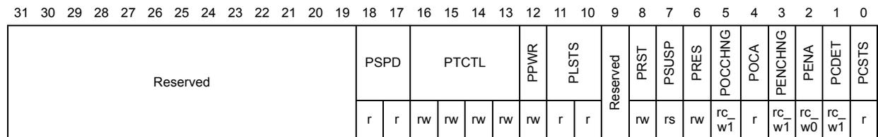
| 31 | 30 | 29 | 28 | 27 | 26 | 25 | 24 | 23 | 22 | 21 | 20 | 19 | 18 | 17 | 16 | 15 | 14 | 13 | 12 | 11 | 10 | 9 | 8 | 7 | 6 | 5 | 4 | 3 | 2 | 1 | 0 |
| Reserved | PSPD | PTCTL | PPWR | PLSTS | Reserved | PRST | PSUSP | PRES | POCCHNG | POCA | PENCHNG | PENA | PCDET | PCSTS | |||||||||||||||||
| r | r | rw | rw | rw | rw | rw | r | r | rw | rs | rw | rc_w1 | r | rc_w1 | rc_w0 | rc_w1 | r | ||||||||||||||
Bits 31:19 Reserved, must be kept at reset value.
Bits 18:17 PSPD : Port speed
Indicates the speed of the device attached to this port.
01: Full speed
10: Low speed
11: Reserved
Bits 16:13 PTCTL : Port test controlThe application writes a nonzero value to this field to put the port into a Test mode, and the corresponding pattern is signaled on the port.
0000: Test mode disabled
0001: Test_J mode
0010: Test_K mode
0011: Test_SE0_NAK mode
0100: Test_Packet mode
0101: Test_Force_Enable
Others: Reserved
Bit 12 PPWR : Port powerThe application uses this field to control power to this port, and the core clears this bit on an overcurrent condition.
0: Power off
1: Power on
Bits 11:10 PLSTS : Port line statusIndicates the current logic level USB data lines
Bit 10: Logic level of OTG_FS_DP
Bit 11: Logic level of OTG_FS_DM
Bit 9 Reserved, must be kept at reset value.
Bit 8 PRST : Port resetWhen the application sets this bit, a reset sequence is started on this port. The application must time the reset period and clear this bit after the reset sequence is complete.
0: Port not in reset
1: Port in reset
The application must leave this bit set for a minimum duration of at least 10 ms to start a reset on the port. The application can leave it set for another 10 ms in addition to the required minimum duration, before clearing the bit, even though there is no maximum limit set by the USB standard.
Bit 7 PSUSP : Port suspendThe application sets this bit to put this port in Suspend mode. The core only stops sending SOFs when this is set. To stop the PHY clock, the application must set the Port clock stop bit, which asserts the suspend input pin of the PHY.
The read value of this bit reflects the current suspend status of the port. This bit is cleared by the core after a remote wake-up signal is detected or the application sets the Port reset bit or Port resume bit in this register or the Resume/remote wake-up detected interrupt bit or Disconnect detected interrupt bit in the Core interrupt register (WKUINT or DISCINT in OTG_FS_GINTSTS, respectively).
0: Port not in Suspend mode
1: Port in Suspend mode
Bit 6 PRES : Port resumeThe application sets this bit to drive resume signaling on the port. The core continues to drive the resume signal until the application clears this bit.
If the core detects a USB remote wake-up sequence, as indicated by the Port resume/remote wake-up detected interrupt bit of the Core interrupt register (WKUINT bit in OTG_FS_GINTSTS), the core starts driving resume signaling without application intervention and clears this bit when it detects a disconnect condition. The read value of this bit indicates whether the core is currently driving resume signaling.
0: No resume driven
1: Resume driven
Bit 5 POCCHNG : Port overcurrent change
The core sets this bit when the status of the Port overcurrent active bit (bit 4) in this register changes.
Bit 4 POCA : Port overcurrent active
Indicates the overcurrent condition of the port.
0: No overcurrent condition
1: Overcurrent condition
Bit 3 PENCHNG : Port enable/disable change
The core sets this bit when the status of the Port enable bit 2 in this register changes.
Bit 2 PENA : Port enable
A port is enabled only by the core after a reset sequence, and is disabled by an overcurrent condition, a disconnect condition, or by the application clearing this bit. The application cannot set this bit by a register write. It can only clear it to disable the port. This bit does not trigger any interrupt to the application.
0: Port disabled
1: Port enabled
Bit 1 PCDET : Port connect detected
The core sets this bit when a device connection is detected to trigger an interrupt to the application using the host port interrupt bit in the Core interrupt register (HPRTINT bit in OTG_FS_GINTSTS). The application must write a 1 to this bit to clear the interrupt.
Bit 0 PCSTS : Port connect status
0: No device is attached to the port
1: A device is attached to the port
OTG_FS Host channel-x characteristics register (OTG_FS_HCCHARx)
(x = 0..7, where x = Channel_number)
Address offset: 0x500 + 0x20 * x
Reset value: 0x0000 0000
| 31 | 30 | 29 | 28 | 27 | 26 | 25 | 24 | 23 | 22 | 21 | 20 | 19 | 18 | 17 | 16 | 15 | 14 | 13 | 12 | 11 | 10 | 9 | 8 | 7 | 6 | 5 | 4 | 3 | 2 | 1 | 0 |
|---|---|---|---|---|---|---|---|---|---|---|---|---|---|---|---|---|---|---|---|---|---|---|---|---|---|---|---|---|---|---|---|
| CHENA | CHDIS | ODDFRM | DAD | MCNT | EPTYP | LSDEV | Reserved | EPDIR | EPNUM | MPSIZ | |||||||||||||||||||||
| rs | rs | rw | rw | rw | rw | rw | rw | rw | rw | rw | rw | rw | rw | rw | rw | rw | rw | rw | rw | rw | rw | rw | rw | rw | rw | rw | rw | rw | rw | ||
Bit 31 CHENA : Channel enable
This field is set by the application and cleared by the OTG host.
0: Channel disabled
1: Channel enabled
Bit 30 CHDIS : Channel disable
The application sets this bit to stop transmitting/receiving data on a channel, even before the transfer for that channel is complete. The application must wait for the Channel disabled interrupt before treating the channel as disabled.
Bit 29 ODDFRM : Odd frame
This field is set (reset) by the application to indicate that the OTG host must perform a transfer in an odd frame. This field is applicable for only periodic (isochronous and interrupt) transactions.
0: Even frame
1: Odd frame
Bits 28:22 DAD : Device address
This field selects the specific device serving as the data source or sink.
Bits 21:20 MCNT : Multicount
This field indicates to the host the number of transactions that must be executed per frame for this periodic endpoint. For non-periodic transfers, this field is not used
00: Reserved. This field yields undefined results
01: 1 transaction
10: 2 transactions per frame to be issued for this endpoint
11: 3 transactions per frame to be issued for this endpoint
Note: This field must be set to at least 01.
Bits 19:18 EPTYP : Endpoint type
Indicates the transfer type selected.
00: Control
01: Isochronous
10: Bulk
11: Interrupt
Bit 17 LSDEV : Low-speed device
This field is set by the application to indicate that this channel is communicating to a low-speed device.
Bit 16 Reserved, must be kept at reset value.
Bit 15 EPDIR : Endpoint direction
Indicates whether the transaction is IN or OUT.
0: OUT
1: IN
Bits 14:11 EPNUM : Endpoint number
Indicates the endpoint number on the device serving as the data source or sink.
Bits 10:0 MPSIZ : Maximum packet size
Indicates the maximum packet size of the associated endpoint.
OTG_FS Host channel-x interrupt register (OTG_FS_HCINTx) (x = 0..7, where x = Channel_number)
Address offset: 0x508 + 0x20 * x
Reset value: 0x0000 0000
This register indicates the status of a channel with respect to USB- and AHB-related events. It is shown in Figure 250 . The application must read this register when the host channels interrupt bit in the Core interrupt register (HCINT bit in OTG_FS_GINTSTS) is set. Before the application can read this register, it must first read the host all channels interrupt (OTG_FS_HAINT) register to get the exact channel number for the host channel-x interrupt register. The application must clear the appropriate bit in this register to clear the corresponding bits in the OTG_FS_HAINT and OTG_FS_GINTSTS registers.
| 31 | 30 | 29 | 28 | 27 | 26 | 25 | 24 | 23 | 22 | 21 | 20 | 19 | 18 | 17 | 16 | 15 | 14 | 13 | 12 | 11 | 10 | 9 | 8 | 7 | 6 | 5 | 4 | 3 | 2 | 1 | 0 |
|---|---|---|---|---|---|---|---|---|---|---|---|---|---|---|---|---|---|---|---|---|---|---|---|---|---|---|---|---|---|---|---|
| Reserved | DTERR | FRMOR | BBERR | TXERR | Reserved | ACK | NAK | STALL | Reserved | CHH | XFRC | ||||||||||||||||||||
| rc_w1 | rc_w1 | rc_w1 | rc_w1 | rc_w1 | rc_w1 | rc_w1 | rc_w1 | rc_w1 | |||||||||||||||||||||||
Bits 31:11 Reserved, must be kept at reset value.
Bit 10 DTERR : Data toggle error
Bit 9 FRMOR : Frame overrun
Bit 8 BBERR : Babble error
Bit 7 TXERR : Transaction error
Indicates one of the following errors occurred on the USB.
CRC check failure
Timeout
Bit stuff error
False EOP
Bit 6 Reserved, must be kept at reset value.
Bit 5 ACK : ACK response received/transmitted interrupt
Bit 4 NAK : NAK response received interrupt
Bit 3 STALL : STALL response received interrupt
Bit 2 Reserved, must be kept at reset value.
Bit 1 CHH : Channel halted
Indicates the transfer completed abnormally either because of any USB transaction error or in response to disable request by the application.
Bit 0 XFRC : Transfer completed
Transfer completed normally without any errors.
OTG_FS Host channel-x interrupt mask register (OTG_FS_HCINTMSKx)
(x = 0..7, where x = Channel_number)
Address offset: 0x50C + 0x20 * x
Reset value: 0x0000 0000
This register reflects the mask for each channel status described in the previous section.
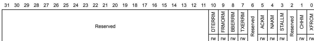
| 31 | 30 | 29 | 28 | 27 | 26 | 25 | 24 | 23 | 22 | 21 | 20 | 19 | 18 | 17 | 16 | 15 | 14 | 13 | 12 | 11 | 10 | 9 | 8 | 7 | 6 | 5 | 4 | 3 | 2 | 1 | 0 |
|---|---|---|---|---|---|---|---|---|---|---|---|---|---|---|---|---|---|---|---|---|---|---|---|---|---|---|---|---|---|---|---|
| Reserved | DTERRM | FRMORM | BBERRM | TXERRM | Reserved | ACKM | NAKM | STALLM | Reserved | CHHM | XFRCM | ||||||||||||||||||||
| rw | rw | rw | rw | rw | rw | rw | |||||||||||||||||||||||||
Bits 31:11 Reserved, must be kept at reset value.
Bit 10 DTERRM : Data toggle error mask
0: Masked interrupt
1: Unmasked interrupt
Bit 9 FRMORM : Frame overrun mask
0: Masked interrupt
1: Unmasked interrupt
Bit 8 BBERRM : Babble error mask
0: Masked interrupt
1: Unmasked interrupt
Bit 7 TXERRM : Transaction error mask
0: Masked interrupt
1: Unmasked interrupt
Bit 6 Reserved, must be kept at reset value.
Bit 5 ACKM : ACK response received/transmitted interrupt mask
0: Masked interrupt
1: Unmasked interrupt
Bit 4 NAKM : NAK response received interrupt mask
0: Masked interrupt
1: Unmasked interrupt
Bit 3 STALLM : STALL response received interrupt mask
0: Masked interrupt
1: Unmasked interrupt
Bit 2 Reserved, must be kept at reset value.
Bit 1 CHHM : Channel halted mask
- 0: Masked interrupt
- 1: Unmasked interrupt
Bit 0 XFRCM : Transfer completed mask
- 0: Masked interrupt
- 1: Unmasked interrupt
OTG_FS Host channel-x transfer size register (OTG_FS_HCTSIZx) (x = 0..7, where x = Channel_number)
Address offset: 0x510 + 0x20 * x
Reset value: 0x0000 0000
| 31 | 30 | 29 | 28 | 27 | 26 | 25 | 24 | 23 | 22 | 21 | 20 | 19 | 18 | 17 | 16 | 15 | 14 | 13 | 12 | 11 | 10 | 9 | 8 | 7 | 6 | 5 | 4 | 3 | 2 | 1 | 0 |
|---|---|---|---|---|---|---|---|---|---|---|---|---|---|---|---|---|---|---|---|---|---|---|---|---|---|---|---|---|---|---|---|
| Reserved | DPID | PKTCNT | |||||||||||||||||||||||||||||
| rw | rw | rw | rw | rw | rw | rw | rw | rw | rw | rw | rw | rw | rw | rw | rw | rw | rw | rw | rw | rw | rw | rw | rw | rw | rw | rw | rw | rw | rw | rw | rw |
Bit 31 Reserved, must be kept at reset value.
Bits 30:29 DPID : Data PID
The application programs this field with the type of PID to use for the initial transaction. The host maintains this field for the rest of the transfer.
- 00: DATA0
- 01: DATA2
- 10: DATA1
- 11: MDATA (non-control)/SETUP (control)
Bits 28:19 PKTCNT : Packet count
This field is programmed by the application with the expected number of packets to be transmitted (OUT) or received (IN).
The host decrements this count on every successful transmission or reception of an OUT/IN packet. Once this count reaches zero, the application is interrupted to indicate normal completion.
Bits 18:0 XFRSIZ : Transfer size
For an OUT, this field is the number of data bytes the host sends during the transfer.
For an IN, this field is the buffer size that the application has reserved for the transfer. The application is expected to program this field as an integer multiple of the maximum packet size for IN transactions (periodic and non-periodic).
22.16.4 Device-mode registers
OTG_FS device configuration register (OTG_FS_DCFG)
Address offset: 0x800
Reset value: 0x0220 0000
This register configures the core in device mode after power-on or after certain control commands or enumeration. Do not make changes to this register after initial programming.
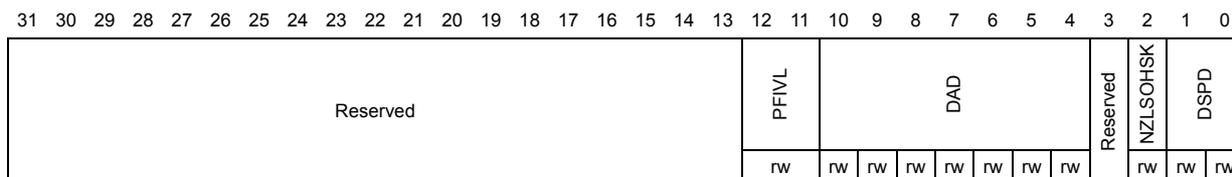
| 31 | 30 | 29 | 28 | 27 | 26 | 25 | 24 | 23 | 22 | 21 | 20 | 19 | 18 | 17 | 16 | 15 | 14 | 13 | 12 | 11 | 10 | 9 | 8 | 7 | 6 | 5 | 4 | 3 | 2 | 1 | 0 |
|---|---|---|---|---|---|---|---|---|---|---|---|---|---|---|---|---|---|---|---|---|---|---|---|---|---|---|---|---|---|---|---|
| Reserved | PFIVL | DAD | Reserved | NZLSOHSK | DSPD | ||||||||||||||||||||||||||
| rw | rw | rw | rw | rw | rw | rw | rw | rw | rw | rw | rw | rw | rw | ||||||||||||||||||
Bits 31:13 Reserved, must be kept at reset value.
Bits 12:11 PFIVL : Periodic frame interval
Indicates the time within a frame at which the application must be notified using the end of periodic frame interrupt. This can be used to determine if all the isochronous traffic for that frame is complete.
00: 80% of the frame interval
01: 85% of the frame interval
10: 90% of the frame interval
11: 95% of the frame interval
Bits 10:4 DAD : Device address
The application must program this field after every SetAddress control command.
Bit 3 Reserved, must be kept at reset value.
Bit 2 NZLSOHSK : Non-zero-length status OUT handshake
The application can use this field to select the handshake the core sends on receiving a nonzero-length data packet during the OUT transaction of a control transfer's Status stage.
1: Send a STALL handshake on a nonzero-length status OUT transaction and do not send the received OUT packet to the application.
0: Send the received OUT packet to the application (zero-length or nonzero-length) and send a handshake based on the NAK and STALL bits for the endpoint in the Device endpoint control register.
Bits 1:0 DSPD : Device speed
Indicates the speed at which the application requires the core to enumerate, or the maximum speed the application can support. However, the actual bus speed is determined only after the chirp sequence is completed, and is based on the speed of the USB host to which the core is connected.
00: Reserved
01: Reserved
10: Reserved
11: Full speed (USB 1.1 transceiver clock is 48 MHz)
OTG_FS device control register (OTG_FS_DCTL)
Address offset: 0x804
Reset value: 0x0000 0000
| 31 | 30 | 29 | 28 | 27 | 26 | 25 | 24 | 23 | 22 | 21 | 20 | 19 | 18 | 17 | 16 | 15 | 14 | 13 | 12 | 11 | 10 | 9 | 8 | 7 | 6 | 5 | 4 | 3 | 2 | 1 | 0 |
|---|---|---|---|---|---|---|---|---|---|---|---|---|---|---|---|---|---|---|---|---|---|---|---|---|---|---|---|---|---|---|---|
| Reserved | POPRGDNE | CGONAK | SGONAK | CGINAK | SGINAK | TCTL | GONSTS | GINSTS | SDIS | RWUSIG | |||||||||||||||||||||
| r/w | w | w | w | w | r/w | r/w | r/w | r | r | r/w | r/w | ||||||||||||||||||||
Bits 31:12 Reserved, must be kept at reset value.
Bit 11 POPRGDNE : Power-on programming done
The application uses this bit to indicate that register programming is completed after a wake-up from power down mode.
Bit 10 CGONAK : Clear global OUT NAK
Writing 1 to this field clears the Global OUT NAK.
Bit 9 SGONAK : Set global OUT NAK
Writing 1 to this field sets the Global OUT NAK.
The application uses this bit to send a NAK handshake on all OUT endpoints.
The application must set the this bit only after making sure that the Global OUT NAK effective bit in the Core interrupt register (GONAKEFF bit in OTG_FS_GINTSTS) is cleared.
Bit 8 CGINAK : Clear global IN NAK
Writing 1 to this field clears the Global IN NAK.
Bit 7 SGINAK : Set global IN NAK
Writing 1 to this field sets the Global non-periodic IN NAK. The application uses this bit to send a NAK handshake on all non-periodic IN endpoints.
The application must set this bit only after making sure that the Global IN NAK effective bit in the Core interrupt register (GINAKEFF bit in OTG_FS_GINTSTS) is cleared.
Bits 6:4 TCTL : Test control
000: Test mode disabled
001: Test_J mode
010: Test_K mode
011: Test_SE0_NAK mode
100: Test_Packet mode
101: Test_Force_Enable
Others: Reserved
Bit 3 GONSTS : Global OUT NAK status
0: A handshake is sent based on the FIFO Status and the NAK and STALL bit settings.
1: No data is written to the RxFIFO, irrespective of space availability. Sends a NAK handshake on all packets, except on SETUP transactions. All isochronous OUT packets are dropped.
Bit 2 GINSTS : Global IN NAK status
0: A handshake is sent out based on the data availability in the transmit FIFO.
1: A NAK handshake is sent out on all non-periodic IN endpoints, irrespective of the data availability in the transmit FIFO.
Bit 1 SDIS : Soft disconnect
The application uses this bit to signal the USB OTG core to perform a soft disconnect. As long as this bit is set, the host does not see that the device is connected, and the device does not receive signals on the USB. The core stays in the disconnected state until the application clears this bit.
0: Normal operation. When this bit is cleared after a soft disconnect, the core generates a device connect event to the USB host. When the device is reconnected, the USB host restarts device enumeration.
1: The core generates a device disconnect event to the USB host.
Bit 0 RWUSIG : Remote wake-up signaling
When the application sets this bit, the core initiates remote signaling to wake up the USB host. The application must set this bit to instruct the core to exit the Suspend state. As specified in the USB 2.0 specification, the application must clear this bit 1 ms to 15 ms after setting it.
Table 134 contains the minimum duration (according to device state) for which the Soft disconnect (SDIS) bit must be set for the USB host to detect a device disconnect. To accommodate clock jitter, it is recommended that the application add some extra delay to the specified minimum duration.
Table 134. Minimum duration for soft disconnect
| Operating speed | Device state | Minimum duration |
|---|---|---|
| Full speed | Suspended | 1 ms + 2.5 µs |
| Full speed | Idle | 2.5 µs |
| Full speed | Not Idle or Suspended (Performing transactions) | 2.5 µs |
OTG_FS device status register (OTG_FS_DSTS)
Address offset: 0x808
Reset value: 0x0000 0010
This register indicates the status of the core with respect to USB-related events. It must be read on interrupts from the device all interrupts (OTG_FS_DAINT) register.
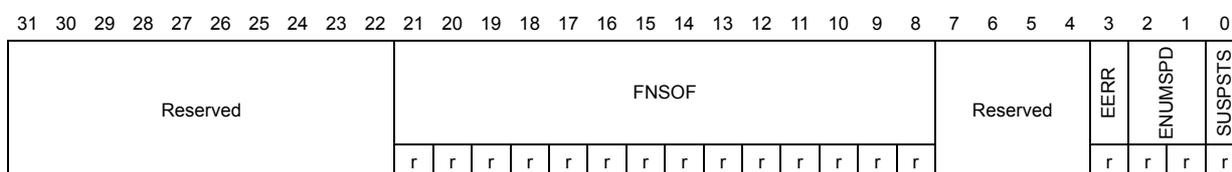
| 31 | 30 | 29 | 28 | 27 | 26 | 25 | 24 | 23 | 22 | 21 | 20 | 19 | 18 | 17 | 16 | 15 | 14 | 13 | 12 | 11 | 10 | 9 | 8 | 7 | 6 | 5 | 4 | 3 | 2 | 1 | 0 |
| Reserved | FNSOF | Reserved | EERR | ENUMSPD | SUSPSTS | ||||||||||||||||||||||||||
| r | r | r | r | r | r | r | r | r | r | r | r | r | r | r | r | r | r | r | r | r | r | r | r | r | r | r | r | r | r | r | r |
Bits 31:22 Reserved, must be kept at reset value.
Bits 21:8 FNSOF : Frame number of the received SOF
Bits 7:4 Reserved, must be kept at reset value.
Bit 3 EERR : Erratic error
The core sets this bit to report any erratic errors.
Due to erratic errors, the OTG_FS controller goes into Suspended state and an interrupt is generated to the application with Early suspend bit of the OTG_FS_GINTSTS register (ESUSP bit in OTG_FS_GINTSTS). If the early suspend is asserted due to an erratic error, the application can only perform a soft disconnect/recover.
Bits 2:1 ENUMSPD : Enumerated speed
Indicates the speed at which the OTG_FS controller has come up after speed detection through a chirp sequence.
01: Reserved
10: Reserved
11: Full speed (PHY clock is running at 48 MHz)
Others: reserved
Bit 0 SUSPSTS : Suspend status
In device mode, this bit is set as long as a Suspend condition is detected on the USB. The core enters the Suspended state when there is no activity on the USB data lines for a period of 3 ms. The core comes out of the suspend:
- – When there is an activity on the USB data lines
- – When the application writes to the Remote wake-up signaling bit in the OTG_FS_DCTL register (RWUSIG bit in OTG_FS_DCTL).
OTG_FS device IN endpoint common interrupt mask register (OTG_FS_DIEPMSK)
Address offset: 0x810
Reset value: 0x0000 0000
This register works with each of the OTG_FS_DIEPINTx registers for all endpoints to generate an interrupt per IN endpoint. The IN endpoint interrupt for a specific status in the OTG_FS_DIEPINTx register can be masked by writing to the corresponding bit in this register. Status bits are masked by default.
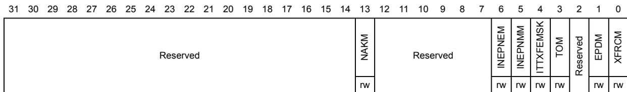
| 31 | 30 | 29 | 28 | 27 | 26 | 25 | 24 | 23 | 22 | 21 | 20 | 19 | 18 | 17 | 16 | 15 | 14 | 13 | 12 | 11 | 10 | 9 | 8 | 7 | 6 | 5 | 4 | 3 | 2 | 1 | 0 |
| Reserved | NAK M | Reserved | INEP NEM | INEP NM | ITT XFEM SK | TOM | Reserved | EP DM | XF RCM | ||||||||||||||||||||||
| r/w | r/w | r/w | r/w | r/w | r/w | r/w | |||||||||||||||||||||||||
Bits 31:14 Reserved, must be kept at reset value.
Bit 13 NAKM : NAK interrupt mask
0: Masked interrupt
1: Unmasked interrupt
Bits 12:7 Reserved, must be kept at reset value.
Bit 6 INEPNE : IN endpoint NAK effective mask
0: Masked interrupt
1: Unmasked interrupt
- Bit 5
INEPNMM
: IN token received with EP mismatch mask
0: Masked interrupt
1: Unmasked interrupt - Bit 4
ITTXFEMSK
: IN token received when TxFIFO empty mask
0: Masked interrupt
1: Unmasked interrupt - Bit 3
TOM
: Timeout condition mask (Non-isochronous endpoints)
0: Masked interrupt
1: Unmasked interrupt - Bit 2 Reserved, must be kept at reset value.
- Bit 1
EPDM
: Endpoint disabled interrupt mask
0: Masked interrupt
1: Unmasked interrupt - Bit 0
XFRCM
: Transfer completed interrupt mask
0: Masked interrupt
1: Unmasked interrupt
OTG_FS device OUT endpoint common interrupt mask register (OTG_FS_DOEPMSK)
Address offset: 0x814
Reset value: 0x0000 0000
This register works with each of the OTG_FS_DOEPINTx registers for all endpoints to generate an interrupt per OUT endpoint. The OUT endpoint interrupt for a specific status in the OTG_FS_DOEPINTx register can be masked by writing into the corresponding bit in this register. Status bits are masked by default.
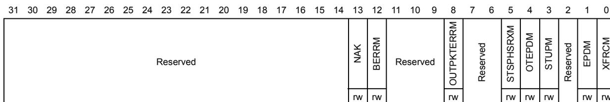
| 31 | 30 | 29 | 28 | 27 | 26 | 25 | 24 | 23 | 22 | 21 | 20 | 19 | 18 | 17 | 16 | 15 | 14 | 13 | 12 | 11 | 10 | 9 | 8 | 7 | 6 | 5 | 4 | 3 | 2 | 1 | 0 |
|---|---|---|---|---|---|---|---|---|---|---|---|---|---|---|---|---|---|---|---|---|---|---|---|---|---|---|---|---|---|---|---|
| Reserved | NAK | BERRM | Reserved | OUTPKTERRM | Reserved | STSPHSRXM | OTEPDM | STUPM | Reserved | EPDM | XFRCM | ||||||||||||||||||||
| rw | rw | rw | rw | rw | rw | rw | |||||||||||||||||||||||||
Bits 31:14 Reserved, must be kept at reset value.
Bit 13 NAKMSK : NAK interrupt mask
- 0: Masked interrupt
1: Unmasked interrupt
Bit 12 BERRM : Babble error interrupt mask
- 0: Masked interrupt
1: Unmasked interrupt
Bits 11:9 Reserved, must be kept at reset value.
Bit 8 OUTPKTERRM : Out packet error mask
- 0: Masked interrupt
1: Unmasked interrupt
Bits 7:6 Reserved, must be kept at reset value.
Bit 5 STSPHSRXM : Status phase received for control write mask
- 0: Masked interrupt
- 1: Unmasked interrupt
Bit 4 OTEPDM : OUT token received when endpoint disabled mask
- Applies to control OUT endpoints only.
- 0: Masked interrupt
- 1: Unmasked interrupt
Bit 3 STUPM : SETUP phase done mask
- Applies to control endpoints only.
- 0: Masked interrupt
- 1: Unmasked interrupt
Bit 2 Reserved, must be kept at reset value.
Bit 1 EPDM : Endpoint disabled interrupt mask
- 0: Masked interrupt
- 1: Unmasked interrupt
Bit 0 XFRCM : Transfer completed interrupt mask
- 0: Masked interrupt
- 1: Unmasked interrupt
OTG_FS device all endpoints interrupt register (OTG_FS_DAINT)
Address offset: 0x818
Reset value: 0x0000 0000
When a significant event occurs on an endpoint, a OTG_FS_DAINT register interrupts the application using the Device OUT endpoints interrupt bit or Device IN endpoints interrupt bit of the OTG_FS_GINTSTS register (OEPINT or IEPINT in OTG_FS_GINTSTS, respectively). There is one interrupt bit per endpoint, up to a maximum of 16 bits for OUT endpoints and 16 bits for IN endpoints. For a bidirectional endpoint, the corresponding IN and OUT interrupt bits are used. Bits in this register are set and cleared when the application sets and clears bits in the corresponding Device Endpoint-x interrupt register (OTG_FS_DIEPINTx/OTG_FS_DOEPINTx).
| 31 | 30 | 29 | 28 | 27 | 26 | 25 | 24 | 23 | 22 | 21 | 20 | 19 | 18 | 17 | 16 | 15 | 14 | 13 | 12 | 11 | 10 | 9 | 8 | 7 | 6 | 5 | 4 | 3 | 2 | 1 | 0 |
|---|---|---|---|---|---|---|---|---|---|---|---|---|---|---|---|---|---|---|---|---|---|---|---|---|---|---|---|---|---|---|---|
| OEPINT | IEPINT | ||||||||||||||||||||||||||||||
| r | r | r | r | r | r | r | r | r | r | r | r | r | r | r | r | r | r | r | r | r | r | r | r | r | r | r | r | r | r | r | r |
Bits 31:16 OEPINT : OUT endpoint interrupt bits
- One bit per OUT endpoint:
- Bit 16 for OUT endpoint 0, bit 19 for OUT endpoint 3.
Bits 15:0 IEPINT : IN endpoint interrupt bits
- One bit per IN endpoint:
- Bit 0 for IN endpoint 0, bit 3 for endpoint 3.
OTG_FS all endpoints interrupt mask register (OTG_FS_DAINMSK)
Address offset: 0x81C
Reset value: 0x0000 0000
The OTG_FS_DAINMSK register works with the Device endpoint interrupt register to interrupt the application when an event occurs on a device endpoint. However, the OTG_FS_DAIN register bit corresponding to that interrupt is still set.

| 31 | 30 | 29 | 28 | 27 | 26 | 25 | 24 | 23 | 22 | 21 | 20 | 19 | 18 | 17 | 16 | 15 | 14 | 13 | 12 | 11 | 10 | 9 | 8 | 7 | 6 | 5 | 4 | 3 | 2 | 1 | 0 |
| OEPM | IEPM | ||||||||||||||||||||||||||||||
| rw | rw | rw | rw | rw | rw | rw | rw | rw | rw | rw | rw | rw | rw | rw | rw | rw | rw | rw | rw | rw | rw | rw | rw | rw | rw | rw | rw | rw | rw | rw | rw |
Bits 31:16 OEPM : OUT EP interrupt mask bits
One per OUT endpoint:
Bit 16 for OUT EP 0, bit 19 for OUT EP 3
0: Masked interrupt
1: Unmasked interrupt
Bits 15:0 IEPM : IN EP interrupt mask bits
One bit per IN endpoint:
Bit 0 for IN EP 0, bit 3 for IN EP 3
0: Masked interrupt
1: Unmasked interrupt
OTG_FS device V BUS discharge time register (OTG_FS_DVBUSDIS)
Address offset: 0x0828
Reset value: 0x0000 17D7
This register specifies the V BUS discharge time after V BUS pulsing during SRP.

| 31 | 30 | 29 | 28 | 27 | 26 | 25 | 24 | 23 | 22 | 21 | 20 | 19 | 18 | 17 | 16 | 15 | 14 | 13 | 12 | 11 | 10 | 9 | 8 | 7 | 6 | 5 | 4 | 3 | 2 | 1 | 0 |
| Reserved | VBUSDT | ||||||||||||||||||||||||||||||
| rw | rw | rw | rw | rw | rw | rw | rw | rw | rw | rw | rw | rw | rw | rw | rw | ||||||||||||||||
Bits 31:16 Reserved, must be kept at reset value.
Bits 15:0 VBUSDT : Device V BUS discharge time
Specifies the V
BUS
discharge time after V
BUS
pulsing during SRP. This value equals:
V
BUS
discharge time in PHY clocks / 1 024
Depending on your V
BUS
load, this value may need adjusting.
OTG_FS device V BUS pulsing time register (OTG_FS_DVBUSPULSE)
Address offset: 0x082C
Reset value: 0x0000 05B8
This register specifies the V BUS pulsing time during SRP.
| 31 | 30 | 29 | 28 | 27 | 26 | 25 | 24 | 23 | 22 | 21 | 20 | 19 | 18 | 17 | 16 | 15 | 14 | 13 | 12 | 11 | 10 | 9 | 8 | 7 | 6 | 5 | 4 | 3 | 2 | 1 | 0 |
|---|---|---|---|---|---|---|---|---|---|---|---|---|---|---|---|---|---|---|---|---|---|---|---|---|---|---|---|---|---|---|---|
| Reserved | DVBUSP | ||||||||||||||||||||||||||||||
| rw | rw | rw | rw | rw | rw | rw | rw | rw | rw | rw | rw | ||||||||||||||||||||
Bits 31:12 Reserved, must be kept at reset value.
Bits 11:0 DVBUSP : Device V BUS pulsing time
Specifies the V BUS pulsing time during SRP. This value equals:
V BUS pulsing time in PHY clocks / 1 024
OTG_FS device IN endpoint FIFO empty interrupt mask register: (OTG_FS_DIEPMPMSK)
Address offset: 0x834
Reset value: 0x0000 0000
This register is used to control the IN endpoint FIFO empty interrupt generation (TXFE_OTG_FS_DIEPINTx).
| 31 | 30 | 29 | 28 | 27 | 26 | 25 | 24 | 23 | 22 | 21 | 20 | 19 | 18 | 17 | 16 | 15 | 14 | 13 | 12 | 11 | 10 | 9 | 8 | 7 | 6 | 5 | 4 | 3 | 2 | 1 | 0 |
|---|---|---|---|---|---|---|---|---|---|---|---|---|---|---|---|---|---|---|---|---|---|---|---|---|---|---|---|---|---|---|---|
| Reserved | INEPTXFEM | ||||||||||||||||||||||||||||||
| rw | rw | rw | rw | rw | rw | rw | rw | rw | rw | rw | rw | rw | rw | rw | rw | ||||||||||||||||
Bits 31:16 Reserved, must be kept at reset value.
Bits 15:0 INEPTXFEM : IN EP Tx FIFO empty interrupt mask bits
These bits act as mask bits for OTG_FS_DIEPINTx.
TXFE interrupt one bit per IN endpoint:
Bit 0 for IN endpoint 0, bit 3 for IN endpoint 3
0: Masked interrupt
1: Unmasked interrupt
OTG_FS device control IN endpoint 0 control register (OTG_FS_DIEPCTL0)
Address offset: 0x900
Reset value: 0x0000 0000
This section describes the OTG_FS_DIEPCTL0 register. Nonzero control endpoints use registers for endpoints 1–3.
| 31 | 30 | 29 | 28 | 27 | 26 | 25 | 24 | 23 | 22 | 21 | 20 | 19 | 18 | 17 | 16 | 15 | 14 | 13 | 12 | 11 | 10 | 9 | 8 | 7 | 6 | 5 | 4 | 3 | 2 | 1 | 0 |
|---|---|---|---|---|---|---|---|---|---|---|---|---|---|---|---|---|---|---|---|---|---|---|---|---|---|---|---|---|---|---|---|
| EPENA | EPDIS | Reserved | SNAK | CNAK | TXFNUM | STALL | Reserved | EPTYP | NAKSTS | Reserved | USBAEP | Reserved | MPSIZ | ||||||||||||||||||
| r | r | w | w | rw | rw | rw | rw | rs | r | r | r | r | rw | rw | |||||||||||||||||
Bit 31 EPENA : Endpoint enable
The application sets this bit to start transmitting data on the endpoint 0.
The core clears this bit before setting any of the following interrupts on this endpoint:
- – Endpoint disabled
- – Transfer completed
Bit 30 EPDIS : Endpoint disable
The application sets this bit to stop transmitting data on an endpoint, even before the transfer for that endpoint is complete. The application must wait for the Endpoint disabled interrupt before treating the endpoint as disabled. The core clears this bit before setting the Endpoint disabled interrupt. The application must set this bit only if Endpoint enable is already set for this endpoint.
Bits 29:28 Reserved, must be kept at reset value.
Bit 27 SNAK : Set NAK
A write to this bit sets the NAK bit for the endpoint.
Using this bit, the application can control the transmission of NAK handshakes on an endpoint. The core can also set this bit for an endpoint after a SETUP packet is received on that endpoint.
Bit 26 CNAK : Clear NAK
A write to this bit clears the NAK bit for the endpoint.
Bits 25:22 TXFNUM : TxFIFO number
This value is set to the FIFO number that is assigned to IN endpoint 0.
Bit 21 STALL : STALL handshake
The application can only set this bit, and the core clears it when a SETUP token is received for this endpoint. If a NAK bit, a Global IN NAK or Global OUT NAK is set along with this bit, the STALL bit takes priority.
Bit 20 Reserved, must be kept at reset value.
Bits 19:18 EPTYP : Endpoint type
Hardcoded to '00' for control.
Bit 17 NAKSTS : NAK status
Indicates the following:
0: The core is transmitting non-NAK handshakes based on the FIFO status
1: The core is transmitting NAK handshakes on this endpoint.
When this bit is set, either by the application or core, the core stops transmitting data, even if there are data available in the TxFIFO. Irrespective of this bit's setting, the core always responds to SETUP data packets with an ACK handshake.
Bit 16 Reserved, must be kept at reset value.
Bit 15 USBAEP : USB active endpoint
This bit is always set to 1, indicating that control endpoint 0 is always active in all configurations and interfaces.
Bits 14:2 Reserved, must be kept at reset value.
Bits 1:0 MPSIZ : Maximum packet size
The application must program this field with the maximum packet size for the current logical endpoint.
00: 64 bytes
01: 32 bytes
10: 16 bytes
11: 8 bytes
OTG device endpoint x control register (OTG_FS_DIEPCTLx) (x = 1..3, where x = Endpoint_number)
Address offset: 0x900 + 0x20 * x
Reset value: 0x0000 0000
The application uses this register to control the behavior of each logical endpoint other than endpoint 0.
| 31 | 30 | 29 | 28 | 27 | 26 | 25 | 24 | 23 | 22 | 21 | 20 | 19 | 18 | 17 | 16 | 15 | 14 | 13 | 12 | 11 | 10 | 9 | 8 | 7 | 6 | 5 | 4 | 3 | 2 | 1 | 0 |
|---|---|---|---|---|---|---|---|---|---|---|---|---|---|---|---|---|---|---|---|---|---|---|---|---|---|---|---|---|---|---|---|
| EPENA | EPDIS | SODDFRM | SDPID/SEVNFRM | SNAK | CNAK | TXFNUM | STALL | Reserved | EPTYP | NAKSTS | EONUM/DPID | USBAEP | Reserved | MPSIZ | |||||||||||||||||
| rs | rs | w | w | w | w | rw | rw | rw | rw | rw | rw | rw | rw | rw | rw | rw | rw | rw | rw | rw | rw | ||||||||||
Bit 31 EPENA : Endpoint enable
The application sets this bit to start transmitting data on an endpoint.
The core clears this bit before setting any of the following interrupts on this endpoint:
- - SETUP phase done
- - Endpoint disabled
- - Transfer completed
Bit 30 EPDIS : Endpoint disable
The application sets this bit to stop transmitting/receiving data on an endpoint, even before the transfer for that endpoint is complete. The application must wait for the Endpoint disabled interrupt before treating the endpoint as disabled. The core clears this bit before setting the Endpoint disabled interrupt. The application must set this bit only if Endpoint enable is already set for this endpoint.
Bit 29 SODDFRM : Set odd frame
Applies to isochronous IN and OUT endpoints only.
Writing to this field sets the Even/Odd frame (EONUM) field to odd frame.
Bit 28 SD0PID: Set DATA0 PIDApplies to interrupt/bulk IN endpoints only.
Writing to this field sets the endpoint data PID (DPID) field in this register to DATA0.
SEVNFRM: Set even frameApplies to isochronous IN endpoints only.
Writing to this field sets the Even/Odd frame (EONUM) field to even frame.
Bit 27 SNAK: Set NAKA write to this bit sets the NAK bit for the endpoint.
Using this bit, the application can control the transmission of NAK handshakes on an endpoint. The core can also set this bit for OUT endpoints on a Transfer completed interrupt, or after a SETUP is received on the endpoint.
Bit 26 CNAK: Clear NAKA write to this bit clears the NAK bit for the endpoint.
Bits 25:22 TXFNUM: TxFIFO numberThese bits specify the FIFO number associated with this endpoint. Each active IN endpoint must be programmed to a separate FIFO number.
This field is valid only for IN endpoints.
Bit 21 STALL: STALL handshakeApplies to non-control, non-isochronous IN endpoints only (access type is rw).
The application sets this bit to stall all tokens from the USB host to this endpoint. If a NAK bit, Global IN NAK, or Global OUT NAK is set along with this bit, the STALL bit takes priority. Only the application can clear this bit, never the core.
Bit 20 Reserved, must be kept at reset value. Bits 19:18 EPTYP: Endpoint typeThis is the transfer type supported by this logical endpoint.
00: Control
01: Isochronous
10: Bulk
11: Interrupt
Bit 17 NAKSTS: NAK statusIt indicates the following:
0: The core is transmitting non-NAK handshakes based on the FIFO status.
1: The core is transmitting NAK handshakes on this endpoint.
When either the application or the core sets this bit:
For non-isochronous IN endpoints: The core stops transmitting any data on an IN endpoint, even if there are data available in the TxFIFO.
For isochronous IN endpoints: The core sends out a zero-length data packet, even if there are data available in the TxFIFO.
Irrespective of this bit's setting, the core always responds to SETUP data packets with an ACK handshake.
Bit 16 EONUM : Even/odd frame
Applies to isochronous IN endpoints only.
Indicates the frame number in which the core transmits/receives isochronous data for this endpoint. The application must program the even/odd frame number in which it intends to transmit/receive isochronous data for this endpoint using the SEVNFRM and SODDFRM fields in this register.
0: Even frame
1: Odd frame
DPID : Endpoint data PID
Applies to interrupt/bulk IN endpoints only.
Contains the PID of the packet to be received or transmitted on this endpoint. The application must program the PID of the first packet to be received or transmitted on this endpoint, after the endpoint is activated. The application uses the SD0PID register field to program either DATA0 or DATA1 PID.
0: DATA0
1: DATA1
Bit 15 USBAEP : USB active endpoint
Indicates whether this endpoint is active in the current configuration and interface. The core clears this bit for all endpoints (other than EP 0) after detecting a USB reset. After receiving the SetConfiguration and SetInterface commands, the application must program endpoint registers accordingly and set this bit.
Bits 14:11 Reserved, must be kept at reset value.
Bits 10:0 MPISZ : Maximum packet size
The application must program this field with the maximum packet size for the current logical endpoint. This value is in bytes.
OTG_FS device control OUT endpoint 0 control register
(OTG_FS_DOEPCTL0)
Address offset: 0xB00
Reset value: 0x0000 8000
This section describes the OTG_FS_DOEPCTL0 register. Nonzero control endpoints use registers for endpoints 1–3.
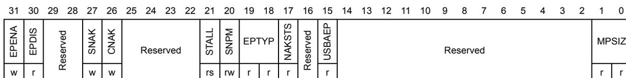
| 31 | 30 | 29 | 28 | 27 | 26 | 25 | 24 | 23 | 22 | 21 | 20 | 19 | 18 | 17 | 16 | 15 | 14 | 13 | 12 | 11 | 10 | 9 | 8 | 7 | 6 | 5 | 4 | 3 | 2 | 1 | 0 |
|---|---|---|---|---|---|---|---|---|---|---|---|---|---|---|---|---|---|---|---|---|---|---|---|---|---|---|---|---|---|---|---|
| EPENA | EPDIS | Reserved | SNAK | CNAK | Reserved | STALL | SNPM | EPTYP | NAKSTS | Reserved | USBAEP | Reserved | MPSIZ | ||||||||||||||||||
| w | r | w | w | rs | rw | r | r | r | r | r | r | r | |||||||||||||||||||
Bit 31 EPENA : Endpoint enable
The application sets this bit to start transmitting data on endpoint 0.
The core clears this bit before setting any of the following interrupts on this endpoint:
- – SETUP phase done
- – Endpoint disabled
- – Transfer completed
Bit 30 EPDIS : Endpoint disable
The application cannot disable control OUT endpoint 0.
Bits 29:28 Reserved, must be kept at reset value.
Bit 27 SNAK : Set NAK
A write to this bit sets the NAK bit for the endpoint.
Using this bit, the application can control the transmission of NAK handshakes on an endpoint. The core can also set this bit on a Transfer completed interrupt, or after a SETUP is received on the endpoint.
Bit 26 CNAK : Clear NAK
A write to this bit clears the NAK bit for the endpoint.
Bits 25:22 Reserved, must be kept at reset value.
Bit 21 STALL : STALL handshake
The application can only set this bit, and the core clears it, when a SETUP token is received for this endpoint. If a NAK bit or Global OUT NAK is set along with this bit, the STALL bit takes priority. Irrespective of this bit's setting, the core always responds to SETUP data packets with an ACK handshake.
Bit 20 SNPM : Snoop mode
This bit configures the endpoint to Snoop mode. In Snoop mode, the core does not check the correctness of OUT packets before transferring them to application memory.
Bits 19:18 EPTYP : Endpoint type
Hardcoded to 2'b00 for control.
Bit 17 NAKSTS : NAK status
Indicates the following:
0: The core is transmitting non-NAK handshakes based on the FIFO status.
1: The core is transmitting NAK handshakes on this endpoint.
When either the application or the core sets this bit, the core stops receiving data, even if there is space in the RxFIFO to accommodate the incoming packet. Irrespective of this bit's setting, the core always responds to SETUP data packets with an ACK handshake.
Bit 16 Reserved, must be kept at reset value.
Bit 15 USBAEP : USB active endpoint
This bit is always set to 1, indicating that a control endpoint 0 is always active in all configurations and interfaces.
Bits 14:2 Reserved, must be kept at reset value.
Bits 1:0 MPSIZ : Maximum packet size
The maximum packet size for control OUT endpoint 0 is the same as what is programmed in control IN endpoint 0.
00: 64 bytes
01: 32 bytes
10: 16 bytes
11: 8 bytes
OTG_FS device endpoint-x control register (OTG_FS_DOEPCTLx) (x = 1..3, where x = Endpoint_number)
Address offset for OUT endpoints: 0xB00 + 0x20 * x
Reset value: 0x0000 0000
The application uses this register to control the behavior of each logical endpoint other than endpoint 0.
| 31 | 30 | 29 | 28 | 27 | 26 | 25 | 24 | 23 | 22 | 21 | 20 | 19 | 18 | 17 | 16 | 15 | 14 | 13 | 12 | 11 | 10 | 9 | 8 | 7 | 6 | 5 | 4 | 3 | 2 | 1 | 0 | |
|---|---|---|---|---|---|---|---|---|---|---|---|---|---|---|---|---|---|---|---|---|---|---|---|---|---|---|---|---|---|---|---|---|
| EPENA | EPDIS | SODDFRM/SD1PID | SDPID/SEVNFRM | SNAK | CNAK | Reserved | STALL | SNPM | EPTYP | NAKSTS | EONUM/DPID | USBAEP | Reserved | MPSIZ | ||||||||||||||||||
| rs | rs | w | w | w | w | rw | rw | rw | r | r | rw | rw | rw | rw | rw | rw | rw | rw | rw | rw | rw | rw | rw | |||||||||
Bit 31 EPENA : Endpoint enable
Applies to IN and OUT endpoints.
The application sets this bit to start transmitting data on an endpoint.
The core clears this bit before setting any of the following interrupts on this endpoint:
- - SETUP phase done
- - Endpoint disabled
- - Transfer completed
The application sets this bit to stop transmitting/receiving data on an endpoint, even before the transfer for that endpoint is complete. The application must wait for the Endpoint disabled interrupt before treating the endpoint as disabled. The core clears this bit before setting the Endpoint disabled interrupt. The application must set this bit only if Endpoint enable is already set for this endpoint.
Bit 29 SD1PID: Set DATA1 PIDApplies to interrupt/bulk IN and OUT endpoints only. Writing to this field sets the endpoint data PID (DPID) field in this register to DATA1.
SODDFRM: Set odd frameApplies to isochronous IN and OUT endpoints only. Writing to this field sets the Even/Odd frame (EONUM) field to odd frame.
Bit 28 SD0PID: Set DATA0 PIDApplies to interrupt/bulk OUT endpoints only.
Writing to this field sets the endpoint data PID (DPID) field in this register to DATA0.
SEVNFRM: Set even frameApplies to isochronous OUT endpoints only.
Writing to this field sets the Even/Odd frame (EONUM) field to even frame.
Bit 27 SNAK: Set NAKA write to this bit sets the NAK bit for the endpoint.
Using this bit, the application can control the transmission of NAK handshakes on an endpoint. The core can also set this bit for OUT endpoints on a Transfer Completed interrupt, or after a SETUP is received on the endpoint.
Bit 26 CNAK: Clear NAKA write to this bit clears the NAK bit for the endpoint.
Bits 25:22 Reserved, must be kept at reset value.
Bit 21 STALL: STALL handshakeApplies to non-control, non-isochronous OUT endpoints only (access type is rw).
The application sets this bit to stall all tokens from the USB host to this endpoint. If a NAK bit, Global IN NAK, or Global OUT NAK is set along with this bit, the STALL bit takes priority. Only the application can clear this bit, never the core.
Bit 20 SNPM: Snoop modeThis bit configures the endpoint to Snoop mode. In Snoop mode, the core does not check the correctness of OUT packets before transferring them to application memory.
Bits 19:18 EPTYP: Endpoint typeThis is the transfer type supported by this logical endpoint.
00: Control
01: Isochronous
10: Bulk
11: Interrupt
Bit 17 NAKSTS: NAK statusIndicates the following:
0: The core is transmitting non-NAK handshakes based on the FIFO status.
1: The core is transmitting NAK handshakes on this endpoint.
When either the application or the core sets this bit:
The core stops receiving any data on an OUT endpoint, even if there is space in the RxFIFO to accommodate the incoming packet.
Irrespective of this bit's setting, the core always responds to SETUP data packets with an ACK handshake.
Bit 16 EONUM: Even/odd frameApplies to isochronous IN and OUT endpoints only.
Indicates the frame number in which the core transmits/receives isochronous data for this endpoint. The application must program the even/odd frame number in which it intends to transmit/receive isochronous data for this endpoint using the SEVNFRM and SODDFRM fields in this register.
0: Even frame
1: Odd frame
DPID: Endpoint data PIDApplies to interrupt/bulk OUT endpoints only.
Contains the PID of the packet to be received or transmitted on this endpoint. The application must program the PID of the first packet to be received or transmitted on this endpoint, after the endpoint is activated. The application uses the SD0PID register field to program either DATA0 or DATA1 PID.
0: DATA0
1: DATA1
Bit 15 USBAEP: USB active endpointIndicates whether this endpoint is active in the current configuration and interface. The core clears this bit for all endpoints (other than EP 0) after detecting a USB reset. After receiving the SetConfiguration and SetInterface commands, the application must program endpoint registers accordingly and set this bit.
Bits 14:11 Reserved, must be kept at reset value.
Bits 10:0 MPSIZ: Maximum packet sizeThe application must program this field with the maximum packet size for the current logical endpoint. This value is in bytes.
OTG_FS device endpoint-x interrupt register (OTG_FS_DIEPINTx) (x = 0..3, where x = Endpoint_number)
Address offset: 0x908 + 0x20 * x
Reset value: 0x0000 0080
This register indicates the status of an endpoint with respect to USB- and AHB-related events. It is shown in Figure 250 . The application must read this register when the IN endpoints interrupt bit of the Core interrupt register (IEPINT in OTG_FS_GINTSTS) is set. Before the application can read this register, it must first read the device all endpoints interrupt (OTG_FS_DAINT) register to get the exact endpoint number for the Device endpoint-x interrupt register. The application must clear the appropriate bit in this register to clear the corresponding bits in the OTG_FS_DAINT and OTG_FS_GINTSTS registers.
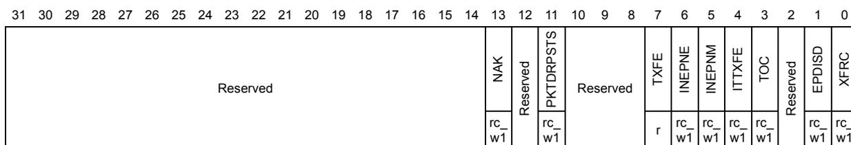
| 31 | 30 | 29 | 28 | 27 | 26 | 25 | 24 | 23 | 22 | 21 | 20 | 19 | 18 | 17 | 16 | 15 | 14 | 13 | 12 | 11 | 10 | 9 | 8 | 7 | 6 | 5 | 4 | 3 | 2 | 1 | 0 |
|---|---|---|---|---|---|---|---|---|---|---|---|---|---|---|---|---|---|---|---|---|---|---|---|---|---|---|---|---|---|---|---|
| Reserved | NAK | Reserved | PKTDRPSTS | Reserved | TXFE | INEPNE | INEPNM | ITTXFE | TOC | Reserved | EPDISD | XFRC | |||||||||||||||||||
| rc_w1 | rc_w1 | r | rc_w1 | rc_w1 | rc_w1 | rc_w1 | rc_w1 | rc_w1 | |||||||||||||||||||||||
Bits 31:14 Reserved, must be kept at reset value.
Bit 13 NAK : NAK input
The core generates this interrupt when a NAK is transmitted or received by the device. In case of isochronous IN endpoints the interrupt gets generated when a zero length packet is transmitted due to unavailability of data in the Tx FIFO.
Bit 12 Reserved, must be kept at reset value.
Bit 11 PKTDRPSTS : Packet dropped status
This bit indicates to the application that an ISOC OUT packet has been dropped. This bit does not have an associated mask bit and does not generate an interrupt.
Bits 10:8 Reserved, must be kept at reset value.
Bit 7 TXFE : Transmit FIFO empty
This interrupt is asserted when the TxFIFO for this endpoint is either half or completely empty. The half or completely empty status is determined by the TxFIFO Empty Level bit in the OTG_FS_GAHBCFG register (TXFELVL bit in OTG_FS_GAHBCFG).
Bit 6 INEPNE : IN endpoint NAK effective
This bit can be cleared when the application clears the IN endpoint NAK by writing to the CNAK bit in OTG_FS_DIEPCTLx.
This interrupt indicates that the core has sampled the NAK bit set (either by the application or by the core). The interrupt indicates that the IN endpoint NAK bit set by the application has taken effect in the core.
This interrupt does not guarantee that a NAK handshake is sent on the USB. A STALL bit takes priority over a NAK bit.
Bit 5 INEPNM : IN token received with EP mismatch.
Indicates that the data in the top of the non-periodic TxFIFO belongs to an endpoint other than the one for which the IN token was received. This interrupt is asserted on the endpoint for which the IN token was received.
Bit 4 ITTXFE : IN token received when TxFIFO is empty
Applies to non-periodic IN endpoints only.
Indicates that an IN token was received when the associated TxFIFO (periodic/non-periodic) was empty. This interrupt is asserted on the endpoint for which the IN token was received.
Bit 3 TOC : Timeout condition
Applies only to Control IN endpoints.
Indicates that the core has detected a timeout condition on the USB for the last IN token on this endpoint.
Bit 2 Reserved, must be kept at reset value.
Bit 1 EPDISD : Endpoint disabled interrupt
This bit indicates that the endpoint is disabled per the application's request.
Bit 0 XFRC : Transfer completed interrupt
This field indicates that the programmed transfer is complete on the AHB as well as on the USB, for this endpoint.
OTG_FS device endpoint-x interrupt register (OTG_FS_DOEPINTx) (x = 0..3, where x = Endpoint_number)
Address offset: 0xB08 + 0x20 * x
Reset value: 0x0000 0080
This register indicates the status of an endpoint with respect to USB- and AHB-related events. It is shown in Figure 250 . The application must read this register when the OUT Endpoints Interrupt bit of the OTG_FS_GINTSTS register (OEPINT bit in OTG_FS_GINTSTS) is set. Before the application can read this register, it must first read the OTG_FS_DAINTR register to get the exact endpoint number for the OTG_FS_DOEPINTx register. The application must clear the appropriate bit in this register to clear the corresponding bits in the OTG_FS_DAINTR and OTG_FS_GINTSTS registers.
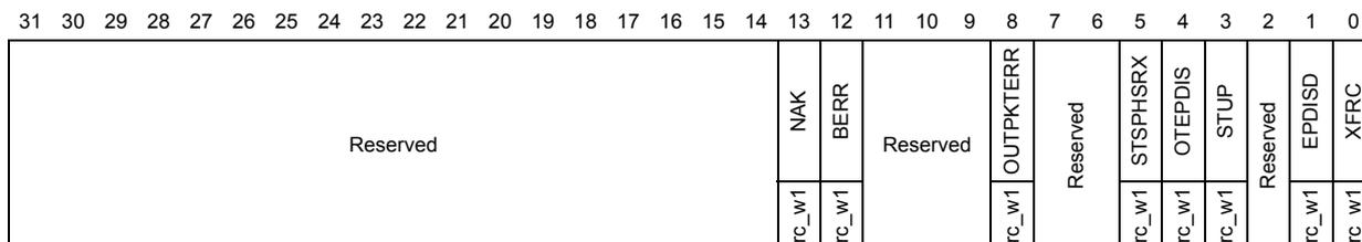
| 31 | 30 | 29 | 28 | 27 | 26 | 25 | 24 | 23 | 22 | 21 | 20 | 19 | 18 | 17 | 16 | 15 | 14 | 13 | 12 | 11 | 10 | 9 | 8 | 7 | 6 | 5 | 4 | 3 | 2 | 1 | 0 |
|---|---|---|---|---|---|---|---|---|---|---|---|---|---|---|---|---|---|---|---|---|---|---|---|---|---|---|---|---|---|---|---|
| Reserved | NAK | BERR | Reserved | OUTPKTERR | Reserved | STSPHSRX | OTEPDIS | STUP | Reserved | EPDISD | XFRC | ||||||||||||||||||||
| rc_w1 | rc_w1 | rc_w1 | rc_w1 | rc_w1 | rc_w1 | rc_w1 | |||||||||||||||||||||||||
Bits 31:14 Reserved, must be kept at reset value.
Bit 13 NAK : NAK input
The core generates this interrupt when a NAK is transmitted or received by the device. In case of isochronous IN endpoints the interrupt gets generated when a zero length packet is transmitted due to unavailability of data in the Tx FIFO.
Bit 12 BERR : Babble error interrupt
The core generates this interrupt when babble is received for the endpoint.
Bits 11:9 Reserved, must be kept at reset value.
Bit 8 OUTPKTERR : OUT packet error
This interrupt is asserted when the core detects an overflow or a CRC error for an OUT packet. This interrupt is valid only when thresholding is enabled.
Bits 7:6 Reserved, must be kept at reset value.
Bit 5 STSPHSRX : Status phase received for control write
This interrupt is generated only after the core has transferred all the data that the host has sent during the data phase of a control write transfer, to the system memory buffer. The interrupt indicates to the application that the host has switched from data phase to the status phase of a control write transfer. The application can use this interrupt to ACK or STALL the status phase, after it has decoded the data phase.
Bit 4 OTEPDIS : OUT token received when endpoint disabled
Applies only to control OUT endpoints.
Indicates that an OUT token was received when the endpoint was not yet enabled. This interrupt is asserted on the endpoint for which the OUT token was received.
Bit 3 STUP : SETUP phase done
Applies to control OUT endpoint only.
Indicates that the SETUP phase for the control endpoint is complete and no more back-to-back SETUP packets were received for the current control transfer. On this interrupt, the application can decode the received SETUP data packet.
Bit 2 Reserved, must be kept at reset value.
Bit 1 EPDISD : Endpoint disabled interrupt
This bit indicates that the endpoint is disabled per the application's request.
Bit 0 XFRC : Transfer completed interrupt
This field indicates that the programmed transfer is complete on the AHB as well as on the USB, for this endpoint.
OTG_FS device IN endpoint 0 transfer size register (OTG_FS_DIEPTSIZ0)
Address offset: 0x910
Reset value: 0x0000 0000
The application must modify this register before enabling endpoint 0. Once endpoint 0 is enabled using the endpoint enable bit in the device control endpoint 0 control registers (EPENA in OTG_FS_DIEPCTL0), the core modifies this register. The application can only read this register once the core has cleared the Endpoint enable bit.
Nonzero endpoints use the registers for endpoints 1–3.

| 31 | 30 | 29 | 28 | 27 | 26 | 25 | 24 | 23 | 22 | 21 | 20 | 19 | 18 | 17 | 16 | 15 | 14 | 13 | 12 | 11 | 10 | 9 | 8 | 7 | 6 | 5 | 4 | 3 | 2 | 1 | 0 | ||||
| Reserved | PKTCNT | Reserved | XFRSIZ | ||||||||||||||||||||||||||||||||
| rw | rw | rw | rw | rw | rw | rw | rw | rw | |||||||||||||||||||||||||||
Bits 31:21 Reserved, must be kept at reset value.
Bits 20:19 PKTCNT : Packet count
Indicates the total number of USB packets that constitute the Transfer Size amount of data for endpoint 0.
This field is decremented every time a packet (maximum size or short packet) is read from the TxFIFO.
Bits 18:7 Reserved, must be kept at reset value.
Bits 6:0 XFRSIZ : Transfer size
Indicates the transfer size in bytes for endpoint 0. The core interrupts the application only after it has exhausted the transfer size amount of data. The transfer size can be set to the maximum packet size of the endpoint, to be interrupted at the end of each packet.
The core decrements this field every time a packet from the external memory is written to the TxFIFO.
OTG_FS device OUT endpoint 0 transfer size register (OTG_FS_DOEPTSIZ0)
Address offset: 0xB10
Reset value: 0x0000 0000
The application must modify this register before enabling endpoint 0. Once endpoint 0 is enabled using the Endpoint enable bit in the OTG_FS_DOEPCTL0 registers (EPENA bit in OTG_FS_DOEPCTL0), the core modifies this register. The application can only read this register once the core has cleared the Endpoint enable bit.
Nonzero endpoints use the registers for endpoints 1–3.
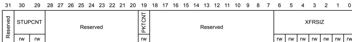
| 31 | 30 | 29 | 28 | 27 | 26 | 25 | 24 | 23 | 22 | 21 | 20 | 19 | 18 | 17 | 16 | 15 | 14 | 13 | 12 | 11 | 10 | 9 | 8 | 7 | 6 | 5 | 4 | 3 | 2 | 1 | 0 | |||||||
| Reserved | STUPCNT | Reserved | PKTCNT | Reserved | XFRSIZ | |||||||||||||||||||||||||||||||||
| rw | rw | rw | rw | rw | rw | rw | rw | rw | ||||||||||||||||||||||||||||||
Bit 31 Reserved, must be kept at reset value.
Bits 30:29 STUPCNT : SETUP packet count
This field specifies the number of back-to-back SETUP data packets the endpoint can receive.
01: 1 packet
10: 2 packets
11: 3 packets
Bits 28:20 Reserved, must be kept at reset value.
Bit 19 PKTCNT : Packet count
This field is decremented to zero after a packet is written into the RxFIFO.
Bits 18:7 Reserved, must be kept at reset value.
Bits 6:0 XFRSIZ : Transfer size
Indicates the transfer size in bytes for endpoint 0. The core interrupts the application only after it has exhausted the transfer size amount of data. The transfer size can be set to the maximum packet size of the endpoint, to be interrupted at the end of each packet.
The core decrements this field every time a packet is read from the RxFIFO and written to the external memory.
OTG_FS device endpoint-x transfer size register (OTG_FS_DIEPTSIZx)
(x = 1..3, where x = Endpoint_number)
Address offset: 0x910 + 0x20 * x
Reset value: 0x0000 0000
The application must modify this register before enabling the endpoint. Once the endpoint is enabled using the Endpoint enable bit in the OTG_FS_DIEPCTLx registers (EPENA bit in OTG_FS_DIEPCTLx), the core modifies this register. The application can only read this register once the core has cleared the Endpoint enable bit.
| 31 | 30 | 29 | 28 | 27 | 26 | 25 | 24 | 23 | 22 | 21 | 20 | 19 | 18 | 17 | 16 | 15 | 14 | 13 | 12 | 11 | 10 | 9 | 8 | 7 | 6 | 5 | 4 | 3 | 2 | 1 | 0 |
|---|---|---|---|---|---|---|---|---|---|---|---|---|---|---|---|---|---|---|---|---|---|---|---|---|---|---|---|---|---|---|---|
| Reserved | PKTCNT | XFRSIZ | |||||||||||||||||||||||||||||
| rw | rw | rw | rw | rw | rw | rw | rw | rw | rw | rw | rw | rw | rw | rw | rw | rw | rw | rw | rw | rw | rw | rw | rw | rw | rw | rw | rw | rw | |||
Bits 31:29 Reserved, must be kept at reset value.
Bit 28:19 PKTCNT: Packet count
Indicates the total number of USB packets that constitute the Transfer Size amount of data for this endpoint.
This field is decremented every time a packet (maximum size or short packet) is read from the TxFIFO.
Bits 18:0 XFRSIZ: Transfer size
This field contains the transfer size in bytes for the current endpoint. The core only interrupts the application after it has exhausted the transfer size amount of data. The transfer size can be set to the maximum packet size of the endpoint, to be interrupted at the end of each packet.
The core decrements this field every time a packet from the external memory is written to the TxFIFO.
OTG_FS device IN endpoint transmit FIFO status register
(OTG_FS_DTXFSTSx) (x = 0..3, where x = Endpoint_number)
Address offset for IN endpoints: \( 0x918 + 0x20 * x \)
This read-only register contains the free space information for the Device IN endpoint TxFIFO.

| 31 | 30 | 29 | 28 | 27 | 26 | 25 | 24 | 23 | 22 | 21 | 20 | 19 | 18 | 17 | 16 | 15 | 14 | 13 | 12 | 11 | 10 | 9 | 8 | 7 | 6 | 5 | 4 | 3 | 2 | 1 | 0 |
| Reserved | INEPTFSAV | ||||||||||||||||||||||||||||||
| r | r | r | r | r | r | r | r | r | r | r | r | r | r | r | r | ||||||||||||||||
31:16 Reserved, must be kept at reset value.
15:0 INEPTFSAV : IN endpoint TxFIFO space available
Indicates the amount of free space available in the Endpoint TxFIFO.
Values are in terms of 32-bit words:
- 0x0: Endpoint TxFIFO is full
- 0x1: 1 word available
- 0x2: 2 words available
- 0xn: n words available
- Others: Reserved
OTG_FS device OUT endpoint-x transfer size register (OTG_FS_DOEPTSIZx)
(x = 1..3, where x = Endpoint_number)
Address offset: \( 0xB10 + 0x20 * x \)
Reset value: 0x0000 0000
The application must modify this register before enabling the endpoint. Once the endpoint is enabled using Endpoint Enable bit of the OTG_FS_DOEPCTLx registers (EPENA bit in OTG_FS_DOEPCTLx), the core modifies this register. The application can only read this register once the core has cleared the Endpoint enable bit.

| 31 | 30 | 29 | 28 | 27 | 26 | 25 | 24 | 23 | 22 | 21 | 20 | 19 | 18 | 17 | 16 | 15 | 14 | 13 | 12 | 11 | 10 | 9 | 8 | 7 | 6 | 5 | 4 | 3 | 2 | 1 | 0 |
| Reserved | RXDPID/S TUPCNT | PKTCNT | XFRSIZ | ||||||||||||||||||||||||||||
| r/rw | r/rw | rw | rw | rw | rw | rw | rw | rw | rw | rw | rw | rw | rw | rw | rw | rw | rw | rw | rw | rw | rw | rw | rw | rw | rw | rw | rw | rw | |||
Bit 31 Reserved, must be kept at reset value.
Bits 30:29 RXDPID : Received data PID
Applies to isochronous OUT endpoints only.
This is the data PID received in the last packet for this endpoint.
- 00: DATA0
- 01: DATA2
- 10: DATA1
- 11: MDATA
Applies to control OUT Endpoints only.
This field specifies the number of back-to-back SETUP data packets the endpoint can receive.
01: 1 packet
10: 2 packets
11: 3 packets
Bit 28:19 PKTCNT: Packet countIndicates the total number of USB packets that constitute the Transfer Size amount of data for this endpoint.
This field is decremented every time a packet (maximum size or short packet) is written to the RxFIFO.
Bits 18:0 XFRSIZ: Transfer sizeThis field contains the transfer size in bytes for the current endpoint. The core only interrupts the application after it has exhausted the transfer size amount of data. The transfer size can be set to the maximum packet size of the endpoint, to be interrupted at the end of each packet.
The core decrements this field every time a packet is read from the RxFIFO and written to the external memory.
22.16.5 OTG_FS power and clock gating control register (OTG_FS_PCGCTL)
Address offset: 0xE00
Reset value: 0x0000 0000
This register is available in host and device modes.
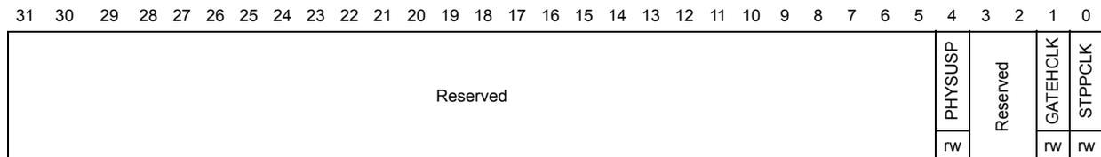
| 31 | 30 | 29 | 28 | 27 | 26 | 25 | 24 | 23 | 22 | 21 | 20 | 19 | 18 | 17 | 16 | 15 | 14 | 13 | 12 | 11 | 10 | 9 | 8 | 7 | 6 | 5 | 4 | 3 | 2 | 1 | 0 | |
| Reserved | PHYSUSP | Reserved | GATEHCLK | STPPCLK | ||||||||||||||||||||||||||||
| rw | rw | rw | ||||||||||||||||||||||||||||||
Bit 31:5 Reserved, must be kept at reset value.
Bit 4 PHYSUSP: PHY SuspendedIndicates that the PHY has been suspended. This bit is updated once the PHY is suspended after the application has set the STPPCLK bit (bit 0).
Bits 3:2 Reserved, must be kept at reset value.
Bit 1 GATEHCLK: Gate HCLKThe application sets this bit to gate HCLK to modules other than the AHB Slave and Master and wake-up logic when the USB is suspended or the session is not valid. The application clears this bit when the USB is resumed or a new session starts.
Bit 0 STPPCLK: Stop PHY clockThe application sets this bit to stop the PHY clock when the USB is suspended, the session is not valid, or the device is disconnected. The application clears this bit when the USB is resumed or a new session starts.
22.16.6 OTG_FS register map
The table below gives the USB OTG register map and reset values.
Table 135. OTG_FS register map and reset values
| Offset | Register | 31 | 30 | 29 | 28 | 27 | 26 | 25 | 24 | 23 | 22 | 21 | 20 | 19 | 18 | 17 | 16 | 15 | 14 | 13 | 12 | 11 | 10 | 9 | 8 | 7 | 6 | 5 | 4 | 3 | 2 | 1 | 0 |
|---|---|---|---|---|---|---|---|---|---|---|---|---|---|---|---|---|---|---|---|---|---|---|---|---|---|---|---|---|---|---|---|---|---|
| 0x000 | OTG_FS_GOTGCTL | Reserved | BSVLD | ASVLD | DBCT | CIDSTS | Reserved | DHNPEN | HSHNPEN | HNRQ | HNGSCS | Reserved | SRQ | SRQSCS | |||||||||||||||||||
| Reset value | 0 | 0 | 0 | 1 | 0 | 0 | 0 | 0 | 0 | 0 | |||||||||||||||||||||||
| 0x004 | OTG_FS_GOTGINT | Reserved | DBCNDNE | ADTOCHG | HNGDET | Reserved | Reserved | HNSSCHG | SRSSCHG | Reserved | SEDET | Res. | |||||||||||||||||||||
| Reset value | 0 | 0 | 0 | 0 | 0 | 0 | |||||||||||||||||||||||||||
| 0x008 | OTG_FS_GAHBCFG | Reserved | PTXFELVL | TXFELVL | Reserved | GINTMSK | |||||||||||||||||||||||||||
| Reset value | 0 | 0 | 0 | ||||||||||||||||||||||||||||||
| 0x00C | OTG_FS_GUSBCFG | CTXPKT | FDMOD | FHMOD | Reserved | TRDT | HNPCCA | SRPCAP | Reserved | PHYSEL | Reserved | TOTAL | |||||||||||||||||||||
| Reset value | 0 | 0 | 0 | 0 | 0 | 1 | 0 | 0 | 0 | 0 | 0 | 0 | |||||||||||||||||||||
| 0x010 | OTG_FS_GRSTCTL | AHBIDL | Reserved | ||||||||||||||||||||||||||||||
| Reset value | 1 | ||||||||||||||||||||||||||||||||
| 0x014 | OTG_FS_GINTS | WKUINT | SRQINT | DISCINT | CIDSCHG | Reserved | PTXFE | HCINT | HPRTINT | Reserved | IPXFR/INCOMPISOUT | IISOIXFR | OEPINT | IEPINT | Reserved | EOPF | ISOODRP | ENUMDNE | USBRS | USBUSUP | ESUSP | Reserved | GONAKEFF | GINAKEFF | NPTXFE | RXFLVL | SOF | OTGINT | MMIS | CMOD | |||
| Reset value | 0 | 0 | 0 | 0 | 1 | 0 | 0 | 0 | 0 | 0 | 0 | 0 | 0 | 0 | 0 | 0 | 0 | 0 | 0 | 1 | 0 | 0 | 0 | 0 | 0 | ||||||||
| 0x018 | OTG_FS_GINTMSK | WUJIM | SRQIM | DISCINT | CIDSSCHGM | Reserved | PTXFEM | HCIM | PRTIM | Reserved | IPXFRM/IISOOXFRM | IISOIXFRM | OEPINT | IEPINT | Reserved | EOPFM | ISOODRPM | ENUMDNEM | USBRS | USBUSUPM | ESUSPM | Reserved | GONAKEFFM | GINAKEFFM | NPTXFEM | RXFLVLM | SOFM | OTGINT | MMISM | Reserved | |||
| Reset value | 0 | 0 | 0 | 0 | 0 | 0 | 0 | 0 | 0 | 0 | 0 | 0 | 0 | 0 | 0 | 0 | 0 | 0 | 0 | 0 | 0 | 0 | 0 | 0 | 0 | ||||||||
| 0x01C | OTG_FS_GRXSTS TSR (host mode) | Reserved | PKTSTS | DPID | BCNT | CHNUM | |||||||||||||||||||||||||||
| Reset value | 0 | 0 | 0 | 0 | 0 | ||||||||||||||||||||||||||||
| OTG_FS_GRXSTS TSR (Device mode) | Reserved | FRMNUM | PKTSTS | DPID | BCNT | EPNUM | |||||||||||||||||||||||||||
| Reset value | 0 | 0 | 0 | 0 | 0 | 0 | 0 | 0 | 0 | 0 | |||||||||||||||||||||||
Table 135. OTG_FS register map and reset values (continued)
| Offset | Register | 31 | 30 | 29 | 28 | 27 | 26 | 25 | 24 | 23 | 22 | 21 | 20 | 19 | 18 | 17 | 16 | 15 | 14 | 13 | 12 | 11 | 10 | 9 | 8 | 7 | 6 | 5 | 4 | 3 | 2 | 1 | 0 |
|---|---|---|---|---|---|---|---|---|---|---|---|---|---|---|---|---|---|---|---|---|---|---|---|---|---|---|---|---|---|---|---|---|---|
| 0x020 | OTG_FS_GRXS TSR (host mode) | Reserved | PKTSTS | DPID | BCNT | CHNUM | |||||||||||||||||||||||||||
| Reset value | 0 | 0 | 0 | 0 | 0 | 0 | 0 | 0 | 0 | 0 | 0 | 0 | 0 | 0 | 0 | 0 | 0 | 0 | 0 | 0 | |||||||||||||
| OTG_FS_GRXS TSPR (Device mode) | Reserved | FRMNUM | PKTSTS | DPID | BCNT | EPNUM | |||||||||||||||||||||||||||
| Reset value | 0 | 0 | 0 | 0 | 0 | 0 | 0 | 0 | 0 | 0 | 0 | 0 | 0 | 0 | 0 | 0 | 0 | 0 | 0 | 0 | 0 | 0 | 0 | 0 | |||||||||
| 0x024 | OTG_FS_GRXF SIZ | Reserved | RXFD | ||||||||||||||||||||||||||||||
| Reset value | 0 | 0 | 0 | 0 | 0 | 0 | 0 | 1 | 0 | 0 | 0 | 0 | 0 | 0 | 0 | 0 | |||||||||||||||||
| 0x028 | OTG_FS_HNPT XFSIZ/ OTG_FS_DIEPT XF0 | NPTXFD/TX0FD | NPTXFSA/TX0FSA | ||||||||||||||||||||||||||||||
| Reset value | 0 | 0 | 0 | 0 | 0 | 0 | 0 | 0 | 0 | 0 | 0 | 0 | 0 | 0 | 0 | 0 | 0 | 0 | 0 | 0 | 0 | 0 | 0 | 1 | 0 | 0 | 0 | 0 | 0 | 0 | 0 | 0 | |
| 0x02C | OTG_FS_HNPT XSTS | Res. | NPTXQTOP | NPTQXSAV | NPTXFSAV | ||||||||||||||||||||||||||||
| Reset value | 0 | 0 | 0 | 0 | 0 | 0 | 0 | 0 | 0 | 0 | 0 | 0 | 0 | 1 | 0 | 0 | 0 | 0 | 0 | 0 | 0 | 0 | 1 | 0 | 0 | 0 | 0 | 0 | 0 | 0 | 0 | ||
| 0x038 | OTG_FS_ GCCFG | Reserved | NOVBUSSENS | SOFOUTEN | VBUSBSEN | VBUSASEN | Reserved | .PWRDWN | Reserved | ||||||||||||||||||||||||
| Reset value | 0 | 0 | 0 | 0 | 0 | ||||||||||||||||||||||||||||
| 0x03C | OTG_FS_CID | PRODUCT_ID | |||||||||||||||||||||||||||||||
| Reset value | 0 | 0 | 0 | 0 | 0 | 0 | 0 | 0 | 0 | 0 | 0 | 0 | 0 | 0 | 0 | 0 | 0 | 0 | 0 | 1 | 0 | 0 | 1 | 0 | 0 | 0 | 0 | 0 | 0 | 0 | 0 | 0 | |
| 0x100 | OTG_FS_HPTX FSIZ | PTXFSIZ | PTXSA | ||||||||||||||||||||||||||||||
| Reset value | 0 | 0 | 0 | 0 | 0 | 0 | 1 | 0 | 0 | 0 | 0 | 0 | 0 | 0 | 0 | 0 | 0 | 0 | 0 | 0 | 0 | 0 | 1 | 0 | 0 | 0 | 0 | 0 | 0 | 0 | 0 | 0 | |
| 0x104 | OTG_FS_DIEPT XF1 | INEPTXFD | INEPTXSA | ||||||||||||||||||||||||||||||
| Reset value | 0 | 0 | 0 | 0 | 0 | 0 | 1 | 0 | 0 | 0 | 0 | 0 | 0 | 0 | 0 | 0 | 0 | 0 | 0 | 0 | 0 | 0 | 1 | 0 | 0 | 0 | 0 | 0 | 0 | 0 | 0 | 0 | |
| 0x108 | OTG_FS_DIEPT XF2 | INEPTXFD | INEPTXSA | ||||||||||||||||||||||||||||||
| Reset value | 0 | 0 | 0 | 0 | 0 | 0 | 1 | 0 | 0 | 0 | 0 | 0 | 0 | 0 | 0 | 0 | 0 | 0 | 0 | 0 | 0 | 0 | 1 | 0 | 0 | 0 | 0 | 0 | 0 | 0 | 0 | 0 | |
| 0x10C | OTG_FS_DIEPT XF3 | INEPTXFD | INEPTXSA | ||||||||||||||||||||||||||||||
| Reset value | 0 | 0 | 0 | 0 | 0 | 0 | 1 | 0 | 0 | 0 | 0 | 0 | 0 | 0 | 0 | 0 | 0 | 0 | 0 | 0 | 0 | 0 | 1 | 0 | 0 | 0 | 0 | 0 | 0 | 0 | 0 | 0 | |
| 0x400 | OTG_FS_HCFG | Reserved | FSLSS | FSLSPCS | |||||||||||||||||||||||||||||
| Reset value | 0 | 0 | 0 | ||||||||||||||||||||||||||||||
| 0x404 | OTG_FS_HFIR | Reserved | FRIVL | ||||||||||||||||||||||||||||||
| Reset value | 1 | 1 | 1 | 0 | 1 | 0 | 1 | 0 | 0 | 1 | 1 | 0 | 0 | 0 | 0 | 0 | |||||||||||||||||
| 0x408 | OTG_FS_HFNU M | FTREM | FRNUM | ||||||||||||||||||||||||||||||
| Reset value | 0 | 0 | 0 | 0 | 0 | 0 | 0 | 0 | 0 | 0 | 0 | 0 | 0 | 0 | 0 | 0 | 0 | 0 | 1 | 1 | 1 | 1 | 1 | 1 | 1 | 1 | 1 | 1 | 1 | 1 | 1 | 1 | |
Table 135. OTG_FS register map and reset values (continued)
| Offset | Register | 31 | 30 | 29 | 28 | 27 | 26 | 25 | 24 | 23 | 22 | 21 | 20 | 19 | 18 | 17 | 16 | 15 | 14 | 13 | 12 | 11 | 10 | 9 | 8 | 7 | 6 | 5 | 4 | 3 | 2 | 1 | 0 |
|---|---|---|---|---|---|---|---|---|---|---|---|---|---|---|---|---|---|---|---|---|---|---|---|---|---|---|---|---|---|---|---|---|---|
| 0x410 | OTG_FS_HPTXSTS | PTXQTOP | PTXQSAV | PTXFSAVL | |||||||||||||||||||||||||||||
| Reset value | 0 | 0 | 0 | 0 | 0 | 0 | 0 | Y | Y | Y | Y | Y | Y | Y | Y | Y | Y | Y | Y | Y | Y | Y | Y | Y | Y | Y | Y | Y | Y | Y | Y | Y | |
| 0x414 | OTG_FS_HAINT | Reserved | HAINT | ||||||||||||||||||||||||||||||
| Reset value | 0 | 0 | 0 | 0 | 0 | 0 | 0 | 0 | 0 | 0 | 0 | 0 | 0 | 0 | 0 | 0 | |||||||||||||||||
| 0x418 | OTG_FS_HAINTMSK | Reserved | HAINTM | ||||||||||||||||||||||||||||||
| Reset value | 0 | 0 | 0 | 0 | 0 | 0 | 0 | 0 | 0 | 0 | 0 | 0 | 0 | 0 | 0 | 0 | |||||||||||||||||
| 0x440 | OTG_FS_HPRT | Reserved | PSPD | PTCTL | PPWR | PLSTS | Res. | PRST | PSUSP | PRES | POCCHNG | POCA | PENCHNG | PENA | PCDET | PCSTS | |||||||||||||||||
| Reset value | 0 | 0 | 0 | 0 | 0 | 0 | 0 | 0 | 0 | 0 | 0 | 0 | 0 | 0 | 0 | 0 | 0 | 0 | 0 | ||||||||||||||
| 0x500 | OTG_FS_HCCHAR0 | CHENA | CHDIS | ODDFRM | DAD | MCNT | EPTYP | LSDEV | Res. | EPDIR | EPNUM | MPSIZ | |||||||||||||||||||||
| Reset value | 0 | 0 | 0 | 0 | 0 | 0 | 0 | 0 | 0 | 0 | 0 | 0 | 0 | 0 | 0 | 0 | 0 | 0 | 0 | 0 | 0 | 0 | 0 | 0 | 0 | 0 | 0 | 0 | 0 | ||||
| 0x520 | OTG_FS_HCCHAR1 | CHENA | CHDIS | ODDFRM | DAD | MCNT | EPTYP | LSDEV | Res. | EPDIR | EPNUM | MPSIZ | |||||||||||||||||||||
| Reset value | 0 | 0 | 0 | 0 | 0 | 0 | 0 | 0 | 0 | 0 | 0 | 0 | 0 | 0 | 0 | 0 | 0 | 0 | 0 | 0 | 0 | 0 | 0 | 0 | 0 | 0 | 0 | 0 | 0 | ||||
| 0x540 | OTG_FS_HCCHAR2 | CHENA | CHDIS | ODDFRM | DAD | MCNT | EPTYP | LSDEV | Res. | EPDIR | EPNUM | MPSIZ | |||||||||||||||||||||
| Reset value | 0 | 0 | 0 | 0 | 0 | 0 | 0 | 0 | 0 | 0 | 0 | 0 | 0 | 0 | 0 | 0 | 0 | 0 | 0 | 0 | 0 | 0 | 0 | 0 | 0 | 0 | 0 | 0 | 0 | ||||
| 0x560 | OTG_FS_HCCHAR3 | CHENA | CHDIS | ODDFRM | DAD | MCNT | EPTYP | LSDEV | Res. | EPDIR | EPNUM | MPSIZ | |||||||||||||||||||||
| Reset value | 0 | 0 | 0 | 0 | 0 | 0 | 0 | 0 | 0 | 0 | 0 | 0 | 0 | 0 | 0 | 0 | 0 | 0 | 0 | 0 | 0 | 0 | 0 | 0 | 0 | 0 | 0 | 0 | 0 | ||||
| 0x580 | OTG_FS_HCCHAR4 | CHENA | CHDIS | ODDFRM | DAD | MCNT | EPTYP | LSDEV | Res. | EPDIR | EPNUM | MPSIZ | |||||||||||||||||||||
| Reset value | 0 | 0 | 0 | 0 | 0 | 0 | 0 | 0 | 0 | 0 | 0 | 0 | 0 | 0 | 0 | 0 | 0 | 0 | 0 | 0 | 0 | 0 | 0 | 0 | 0 | 0 | 0 | 0 | 0 | ||||
| 0x5A0 | OTG_FS_HCCHAR5 | CHENA | CHDIS | ODDFRM | DAD | MCNT | EPTYP | LSDEV | Res. | EPDIR | EPNUM | MPSIZ | |||||||||||||||||||||
| Reset value | 0 | 0 | 0 | 0 | 0 | 0 | 0 | 0 | 0 | 0 | 0 | 0 | 0 | 0 | 0 | 0 | 0 | 0 | 0 | 0 | 0 | 0 | 0 | 0 | 0 | 0 | 0 | 0 | 0 | ||||
| 0x5C0 | OTG_FS_HCCHAR6 | CHENA | CHDIS | ODDFRM | DAD | MCNT | EPTYP | LSDEV | Res. | EPDIR | EPNUM | MPSIZ | |||||||||||||||||||||
| Reset value | 0 | 0 | 0 | 0 | 0 | 0 | 0 | 0 | 0 | 0 | 0 | 0 | 0 | 0 | 0 | 0 | 0 | 0 | 0 | 0 | 0 | 0 | 0 | 0 | 0 | 0 | 0 | 0 | 0 | ||||
| 0x5E0 | OTG_FS_HCCHAR7 | CHENA | CHDIS | ODDFRM | DAD | MCNT | EPTYP | LSDEV | Res. | EPDIR | EPNUM | MPSIZ | |||||||||||||||||||||
| Reset value | 0 | 0 | 0 | 0 | 0 | 0 | 0 | 0 | 0 | 0 | 0 | 0 | 0 | 0 | 0 | 0 | 0 | 0 | 0 | 0 | 0 | 0 | 0 | 0 | 0 | 0 | 0 | 0 | 0 | ||||
| 0x508 | OTG_FS_HCINT0 | Reserved | DTERR | FRMOR | BBERR | TXERR | Res. | ACK | NAK | STALL | Res. | CHH | XFRC | ||||||||||||||||||||
| Reset value | 0 | 0 | 0 | 0 | 0 | 0 | 0 | 0 | 0 | 0 | 0 | ||||||||||||||||||||||
Table 135. OTG_FS register map and reset values (continued)
| Offset | Register | 31 | 30 | 29 | 28 | 27 | 26 | 25 | 24 | 23 | 22 | 21 | 20 | 19 | 18 | 17 | 16 | 15 | 14 | 13 | 12 | 11 | 10 | 9 | 8 | 7 | 6 | 5 | 4 | 3 | 2 | 1 | 0 |
|---|---|---|---|---|---|---|---|---|---|---|---|---|---|---|---|---|---|---|---|---|---|---|---|---|---|---|---|---|---|---|---|---|---|
| 0x528 | OTG_FS_HCINT1 | Reserved | DTERR | FRMOR | BBERR | TXERR | Reserved | ACK | NAK | STALL | Reserved | CHH | XFRC | ||||||||||||||||||||
| Reset value | 0 | 0 | 0 | 0 | 0 | 0 | 0 | 0 | 0 | ||||||||||||||||||||||||
| 0x548 | OTG_FS_HCINT2 | Reserved | DTERR | FRMOR | BBERR | TXERR | Reserved | ACK | NAK | STALL | Reserved | CHH | XFRC | ||||||||||||||||||||
| Reset value | 0 | 0 | 0 | 0 | 0 | 0 | 0 | 0 | 0 | ||||||||||||||||||||||||
| 0x568 | OTG_FS_HCINT3 | Reserved | DTERR | FRMOR | BBERR | TXERR | Reserved | ACK | NAK | STALL | Reserved | CHH | XFRC | ||||||||||||||||||||
| Reset value | 0 | 0 | 0 | 0 | 0 | 0 | 0 | 0 | 0 | ||||||||||||||||||||||||
| 0x588 | OTG_FS_HCINT4 | Reserved | DTERR | FRMOR | BBERR | TXERR | Reserved | ACK | NAK | STALL | Reserved | CHH | XFRC | ||||||||||||||||||||
| Reset value | 0 | 0 | 0 | 0 | 0 | 0 | 0 | 0 | 0 | ||||||||||||||||||||||||
| 0x5A8 | OTG_FS_HCINT5 | Reserved | DTERR | FRMOR | BBERR | TXERR | Reserved | ACK | NAK | STALL | Reserved | CHH | XFRC | ||||||||||||||||||||
| Reset value | 0 | 0 | 0 | 0 | 0 | 0 | 0 | 0 | 0 | ||||||||||||||||||||||||
| 0x5C8 | OTG_FS_HCINT6 | Reserved | DTERR | FRMOR | BBERR | TXERR | Reserved | ACK | NAK | STALL | Reserved | CHH | XFRC | ||||||||||||||||||||
| Reset value | 0 | 0 | 0 | 0 | 0 | 0 | 0 | 0 | 0 | ||||||||||||||||||||||||
| 0x5E8 | OTG_FS_HCINT7 | Reserved | DTERR | FRMOR | BBERR | TXERR | Reserved | ACK | NAK | STALL | Reserved | CHH | XFRC | ||||||||||||||||||||
| Reset value | 0 | 0 | 0 | 0 | 0 | 0 | 0 | 0 | 0 | ||||||||||||||||||||||||
| 0x50C | OTG_FS_HCINTMSK0 | Reserved | DTERRM | FRMORM | BBERRM | TXERRM | Reserved | ACKM | NAKM | STALLM | Reserved | CHHM | XFRCM | ||||||||||||||||||||
| Reset value | 0 | 0 | 0 | 0 | 0 | 0 | 0 | 0 | 0 | ||||||||||||||||||||||||
| 0x52C | OTG_FS_HCINTMSK1 | Reserved | DTERRM | FRMORM | BBERRM | TXERRM | Reserved | ACKM | NAKM | STALLM | Reserved | CHHM | XFRCM | ||||||||||||||||||||
| Reset value | 0 | 0 | 0 | 0 | 0 | 0 | 0 | 0 | 0 | ||||||||||||||||||||||||
| 0x54C | OTG_FS_HCINTMSK2 | Reserved | DTERRM | FRMORM | BBERRM | TXERRM | Reserved | ACKM | NAKM | STALLM | Reserved | CHHM | XFRCM | ||||||||||||||||||||
| Reset value | 0 | 0 | 0 | 0 | 0 | 0 | 0 | 0 | 0 | ||||||||||||||||||||||||
| 0x56C | OTG_FS_HCINTMSK3 | Reserved | DTERRM | FRMORM | BBERRM | TXERRM | Reserved | ACKM | NAKM | STALLM | Reserved | CHHM | XFRCM | ||||||||||||||||||||
| Reset value | 0 | 0 | 0 | 0 | 0 | 0 | 0 | 0 | 0 | ||||||||||||||||||||||||
| 0x58C | OTG_FS_HCINTMSK4 | Reserved | DTERRM | FRMORM | BBERRM | TXERRM | Reserved | ACKM | NAKM | STALLM | Reserved | CHHM | XFRCM | ||||||||||||||||||||
| Reset value | 0 | 0 | 0 | 0 | 0 | 0 | 0 | 0 | 0 | ||||||||||||||||||||||||
Table 135. OTG_FS register map and reset values (continued)
| Offset | Register | 31 | 30 | 29 | 28 | 27 | 26 | 25 | 24 | 23 | 22 | 21 | 20 | 19 | 18 | 17 | 16 | 15 | 14 | 13 | 12 | 11 | 10 | 9 | 8 | 7 | 6 | 5 | 4 | 3 | 2 | 1 | 0 |
|---|---|---|---|---|---|---|---|---|---|---|---|---|---|---|---|---|---|---|---|---|---|---|---|---|---|---|---|---|---|---|---|---|---|
| 0x5AC | OTG_FS_HCINT MSK5 | Reserved | DTERRM | FRMORM | BBERRM | TXERRM | Reserved | ACKM | NAKM | STALLM | Reserved | CHHM | XFRCM | ||||||||||||||||||||
| Reset value | 0 | 0 | 0 | 0 | 0 | 0 | 0 | 0 | 0 | 0 | 0 | ||||||||||||||||||||||
| 0x5CC | OTG_FS_HCINT MSK6 | Reserved | DTERRM | FRMORM | BBERRM | TXERRM | Reserved | ACKM | NAKM | STALLM | Reserved | CHHM | XFRCM | ||||||||||||||||||||
| Reset value | 0 | 0 | 0 | 0 | 0 | 0 | 0 | 0 | 0 | 0 | 0 | ||||||||||||||||||||||
| 0x5EC | OTG_FS_HCINT MSK7 | Reserved | DTERRM | FRMORM | BBERRM | TXERRM | Reserved | ACKM | NAKM | STALLM | Reserved | CHHM | XFRCM | ||||||||||||||||||||
| Reset value | 0 | 0 | 0 | 0 | 0 | 0 | 0 | 0 | 0 | 0 | 0 | ||||||||||||||||||||||
| 0x510 | OTG_FS_HCTS I_Z0 | Reserved | DPID | PKTCNT | XFRSIZ | ||||||||||||||||||||||||||||
| Reset value | 0 | 0 | 0 | 0 | 0 | 0 | 0 | 0 | 0 | 0 | 0 | 0 | 0 | 0 | 0 | 0 | 0 | 0 | 0 | 0 | 0 | 0 | 0 | 0 | 0 | 0 | 0 | 0 | 0 | 0 | 0 | ||
| 0x530 | OTG_FS_HCTS I_Z1 | Reserved | DPID | PKTCNT | XFRSIZ | ||||||||||||||||||||||||||||
| Reset value | 0 | 0 | 0 | 0 | 0 | 0 | 0 | 0 | 0 | 0 | 0 | 0 | 0 | 0 | 0 | 0 | 0 | 0 | 0 | 0 | 0 | 0 | 0 | 0 | 0 | 0 | 0 | 0 | 0 | 0 | 0 | ||
| 0x550 | OTG_FS_HCTS I_Z2 | Reserved | DPID | PKTCNT | XFRSIZ | ||||||||||||||||||||||||||||
| Reset value | 0 | 0 | 0 | 0 | 0 | 0 | 0 | 0 | 0 | 0 | 0 | 0 | 0 | 0 | 0 | 0 | 0 | 0 | 0 | 0 | 0 | 0 | 0 | 0 | 0 | 0 | 0 | 0 | 0 | 0 | 0 | ||
| 0x570 | OTG_FS_HCTS I_Z3 | Reserved | DPID | PKTCNT | XFRSIZ | ||||||||||||||||||||||||||||
| Reset value | 0 | 0 | 0 | 0 | 0 | 0 | 0 | 0 | 0 | 0 | 0 | 0 | 0 | 0 | 0 | 0 | 0 | 0 | 0 | 0 | 0 | 0 | 0 | 0 | 0 | 0 | 0 | 0 | 0 | 0 | 0 | ||
| 0x590 | OTG_FS_HCTS I_Z4 | Reserved | DPID | PKTCNT | XFRSIZ | ||||||||||||||||||||||||||||
| Reset value | 0 | 0 | 0 | 0 | 0 | 0 | 0 | 0 | 0 | 0 | 0 | 0 | 0 | 0 | 0 | 0 | 0 | 0 | 0 | 0 | 0 | 0 | 0 | 0 | 0 | 0 | 0 | 0 | 0 | 0 | 0 | ||
| 0x5B0 | OTG_FS_HCTS I_Z5 | Reserved | DPID | PKTCNT | XFRSIZ | ||||||||||||||||||||||||||||
| Reset value | 0 | 0 | 0 | 0 | 0 | 0 | 0 | 0 | 0 | 0 | 0 | 0 | 0 | 0 | 0 | 0 | 0 | 0 | 0 | 0 | 0 | 0 | 0 | 0 | 0 | 0 | 0 | 0 | 0 | 0 | 0 | ||
| 0x5D0 | OTG_FS_HCTS I_Z6 | Reserved | DPID | PKTCNT | XFRSIZ | ||||||||||||||||||||||||||||
| Reset value | 0 | 0 | 0 | 0 | 0 | 0 | 0 | 0 | 0 | 0 | 0 | 0 | 0 | 0 | 0 | 0 | 0 | 0 | 0 | 0 | 0 | 0 | 0 | 0 | 0 | 0 | 0 | 0 | 0 | 0 | 0 | ||
| 0x5F0 | OTG_FS_HCTS I_Z7 | Reserved | DPID | PKTCNT | XFRSIZ | ||||||||||||||||||||||||||||
| Reset value | 0 | 0 | 0 | 0 | 0 | 0 | 0 | 0 | 0 | 0 | 0 | 0 | 0 | 0 | 0 | 0 | 0 | 0 | 0 | 0 | 0 | 0 | 0 | 0 | 0 | 0 | 0 | 0 | 0 | 0 | 0 | ||
| 0x800 | OTG_FS_DCFG | Reserved | |||||||||||||||||||||||||||||||
| Reset value | |||||||||||||||||||||||||||||||||
| 0x804 | OTG_FS_DCTL | Reserved | |||||||||||||||||||||||||||||||
| Reset value | |||||||||||||||||||||||||||||||||
Table 135. OTG_FS register map and reset values (continued)
| Offset | Register | 31 | 30 | 29 | 28 | 27 | 26 | 25 | 24 | 23 | 22 | 21 | 20 | 19 | 18 | 17 | 16 | 15 | 14 | 13 | 12 | 11 | 10 | 9 | 8 | 7 | 6 | 5 | 4 | 3 | 2 | 1 | 0 | |
|---|---|---|---|---|---|---|---|---|---|---|---|---|---|---|---|---|---|---|---|---|---|---|---|---|---|---|---|---|---|---|---|---|---|---|
| 0x808 | OTG_FS_DSTS | Reserved | FNSOF | Reserved | EERR | ENUMSPD | SUSPSTS | |||||||||||||||||||||||||||
| Reset value | 0 | 0 | 0 | 0 | 0 | 0 | 0 | 0 | 0 | 0 | 0 | 0 | 0 | 0 | 0 | 0 | 0 | |||||||||||||||||
| 0x810 | OTG_FS_DIEPMSK | Reserved | NAKMSK | Reserved | INEPNEM | INEPNMM | ITTXFEMSK | TOM | Reserved | EPDM | XFRM | |||||||||||||||||||||||
| Reset value | 0 | 0 | 0 | 0 | 0 | 0 | 0 | |||||||||||||||||||||||||||
| 0x814 | OTG_FS_DOEPMSK | Reserved | NAKMSK | BERRM | Reserved | OUTPKTERRM | Reserved | STSPHSRXEM | OTEPDM | STUPM | Reserved | EPDM | XFRM | |||||||||||||||||||||
| Reset value | 0 | 0 | 0 | 0 | 0 | 0 | 0 | 0 | ||||||||||||||||||||||||||
| 0x818 | OTG_FS_DAINT | OEPINT | IEPINT | |||||||||||||||||||||||||||||||
| Reset value | 0 | 0 | 0 | 0 | 0 | 0 | 0 | 0 | 0 | 0 | 0 | 0 | 0 | 0 | 0 | 0 | 0 | 0 | 0 | 0 | 0 | 0 | 0 | 0 | 0 | 0 | 0 | 0 | 0 | 0 | 0 | 0 | ||
| 0x81C | OTG_FS_DAINTMSK | OEPM | IEPM | |||||||||||||||||||||||||||||||
| Reset value | 0 | 0 | 0 | 0 | 0 | 0 | 0 | 0 | 0 | 0 | 0 | 0 | 0 | 0 | 0 | 0 | 0 | 0 | 0 | 0 | 0 | 0 | 0 | 0 | 0 | 0 | 0 | 0 | 0 | 0 | 0 | 0 | ||
| 0x828 | OTG_FS_DVBUSDIS | Reserved | VBUSDT | |||||||||||||||||||||||||||||||
| Reset value | 0 | 0 | 0 | 1 | 0 | 1 | 1 | 1 | 1 | 1 | 0 | 1 | 0 | 1 | 1 | 1 | ||||||||||||||||||
| 0x82C | OTG_FS_DVBUSPULSE | Reserved | DVBUSP | |||||||||||||||||||||||||||||||
| Reset value | 0 | 1 | 0 | 1 | 1 | 0 | 1 | 1 | 1 | 0 | 0 | 0 | ||||||||||||||||||||||
| 0x834 | OTG_FS_DIEPEMPMSK | Reserved | INEPTXFEM | |||||||||||||||||||||||||||||||
| Reset value | 0 | 0 | 0 | 0 | 0 | 0 | 0 | 0 | 0 | 0 | 0 | 0 | 0 | 0 | 0 | 0 | ||||||||||||||||||
| 0x900 | OTG_FS_DIEPCTL0 | EPENA | EPDIS | Reserved | SNAK | CNAK | TXFNUM | STALL | Reserved | EPTYP | NAKSTS | Reserved | USBAEP | Reserved | MPSIZ | |||||||||||||||||||
| Reset value | 0 | 0 | 0 | 0 | 0 | 0 | 0 | 0 | 0 | 0 | 0 | 0 | 1 | 0 | 0 | |||||||||||||||||||
| 0x918 | TG_FS_DTXFSTS0 | Reserved | INEPTFSAV | |||||||||||||||||||||||||||||||
| Reset value | 0 | 0 | 0 | 0 | 0 | 0 | 1 | 0 | 0 | 0 | 0 | 0 | 0 | 0 | 0 | 0 | ||||||||||||||||||
| 0x920 | OTG_FS_DIEPCTL1 | EPENA | EPDIS | SODDFRM/SD1PID | SD0PID/SEVNFRM | SNAK | CNAK | TXFNUM | STALL | Reserved | EPTYP | NAKSTS | EONUM/DPID | USBAEP | Reserved | MPSIZ | ||||||||||||||||||
| Reset value | 0 | 0 | 0 | 0 | 0 | 0 | 0 | 0 | 0 | 0 | 0 | 0 | 0 | 0 | 0 | 0 | 0 | 0 | 0 | 0 | 0 | 0 | 0 | 0 | 0 | 0 | 0 | |||||||
| 0x938 | TG_FS_DTXFSTS1 | Reserved | INEPTFSAV | |||||||||||||||||||||||||||||||
| Reset value | 0 | 0 | 0 | 0 | 0 | 0 | 1 | 0 | 0 | 0 | 0 | 0 | 0 | 0 | 0 | 0 | ||||||||||||||||||
Table 135. OTG_FS register map and reset values (continued)
| Offset | Register | 31 | 30 | 29 | 28 | 27 | 26 | 25 | 24 | 23 | 22 | 21 | 20 | 19 | 18 | 17 | 16 | 15 | 14 | 13 | 12 | 11 | 10 | 9 | 8 | 7 | 6 | 5 | 4 | 3 | 2 | 1 | 0 |
|---|---|---|---|---|---|---|---|---|---|---|---|---|---|---|---|---|---|---|---|---|---|---|---|---|---|---|---|---|---|---|---|---|---|
| 0x940 | OTG_FS_DIEPC_TL2 | EPENA | EPDIS | SODDFRM | SDOPID/SEVNFRM | SNAK | CNAK | TXFNUM | STALL | Reserved | EPTYP | NAKSTS | EONUM/DPID | USBAEP | Reserved | MPSIZ | |||||||||||||||||
| Reset value | 0 | 0 | 0 | 0 | 0 | 0 | 0 | 0 | 0 | 0 | 0 | 0 | 0 | 0 | 0 | 0 | 0 | 0 | 0 | 0 | 0 | 0 | 0 | 0 | 0 | 0 | 0 | 0 | |||||
| 0x958 | TG_FS_DTXFSTS2 | Reserved | INEPTFSAV | ||||||||||||||||||||||||||||||
| Reset value | 0 | 0 | |||||||||||||||||||||||||||||||
| 0x960 | OTG_FS_DIEPC_TL3 | EPENA | EPDIS | SODDFRM | SDOPID/SEVNFRM | SNAK | CNAK | TXFNUM | STALL | Reserved | EPTYP | NAKSTS | EONUM/DPID | USBAEP | Reserved | MPSIZ | |||||||||||||||||
| Reset value | 0 | 0 | 0 | 0 | 0 | 0 | 0 | 0 | 0 | 0 | 0 | 0 | 0 | 0 | 0 | 0 | 0 | 0 | 0 | 0 | 0 | 0 | 0 | 0 | 0 | 0 | 0 | ||||||
| 0x978 | TG_FS_DTXFSTS3 | Reserved | INEPTFSAV | ||||||||||||||||||||||||||||||
| Reset value | 0 | 0 | |||||||||||||||||||||||||||||||
| 0xB00 | OTG_FS_DOEP_CTL0 | EPENA | EPDIS | Reserved | SNAK | CNAK | Reserved | STALL | SNPM | EPTYP | NAKSTS | Reserved | USBAEP | Reserved | MPSIZ | ||||||||||||||||||
| Reset value | 0 | 0 | 0 | 0 | 0 | 0 | 0 | 0 | 0 | 0 | 0 | 1 | 0 | 0 | |||||||||||||||||||
| 0xB20 | OTG_FS_DOEP_CTL1 | EPENA | EPDIS | SODDFRM | SDOPID/SEVNFRM | SNAK | CNAK | Reserved | STALL | SNPM | EPTYP | NAKSTS | EONUM/DPID | USBAEP | Reserved | MPSIZ | |||||||||||||||||
| Reset value | 0 | 0 | 0 | 0 | 0 | 0 | 0 | 0 | 0 | 0 | 0 | 0 | 0 | 0 | 0 | 0 | 0 | 0 | 0 | 0 | 0 | 0 | 0 | 0 | |||||||||
| 0xB40 | OTG_FS_DOEP_CTL2 | EPENA | EPDIS | SODDFRM | SDOPID/SEVNFRM | SNAK | CNAK | Reserved | STALL | SNPM | EPTYP | NAKSTS | EONUM/DPID | USBAEP | Reserved | MPSIZ | |||||||||||||||||
| Reset value | 0 | 0 | 0 | 0 | 0 | 0 | 0 | 0 | 0 | 0 | 0 | 0 | 0 | 0 | 0 | 0 | 0 | 0 | 0 | 0 | 0 | 0 | 0 | 0 | |||||||||
| 0xB60 | OTG_FS_DOEP_CTL3 | EPENA | EPDIS | SODDFRM | SDOPID/SEVNFRM | SNAK | CNAK | Reserved | STALL | SNPM | EPTYP | NAKSTS | EONUM/DPID | USBAEP | Reserved | MPSIZ | |||||||||||||||||
| Reset value | 0 | 0 | 0 | 0 | 0 | 0 | 0 | 0 | 0 | 0 | 0 | 0 | 0 | 0 | 0 | 0 | 0 | 0 | 0 | 0 | 0 | 0 | 0 | 0 | |||||||||
| 0x908 | OTG_FS_DIEPI_NTO | Reserved | NAK | Reserved | PKTDRPSTS | Reserved | TXFE | INEPNE | INEPNM | ITTXFE | TOC | Reserved | EPDISD | XFRC | |||||||||||||||||||
| Reset value | 0 | 0 | 0 | 0 | 0 | 1 | 0 | 0 | 0 | 0 | 0 | 0 | 0 | ||||||||||||||||||||
Table 135. OTG_FS register map and reset values (continued)
| Offset | Register | 31 | 30 | 29 | 28 | 27 | 26 | 25 | 24 | 23 | 22 | 21 | 20 | 19 | 18 | 17 | 16 | 15 | 14 | 13 | 12 | 11 | 10 | 9 | 8 | 7 | 6 | 5 | 4 | 3 | 2 | 1 | 0 |
|---|---|---|---|---|---|---|---|---|---|---|---|---|---|---|---|---|---|---|---|---|---|---|---|---|---|---|---|---|---|---|---|---|---|
| 0x928 | OTG_FS_DIEPI NT1 | Reserved | NAK | Reserved | PKTDRPSTS | Reserved | TXFE | INEPNE | INEPNM | ITTXFE | TOC | Reserved | EPDISD | XFRC | |||||||||||||||||||
| Reset value | 0 | 0 | 0 | 1 | 0 | 0 | 0 | 0 | 0 | 0 | |||||||||||||||||||||||
| 0x948 | OTG_FS_DIEPI NT2 | Reserved | NAK | Reserved | PKTDRPSTS | Reserved | TXFE | INEPNE | INEPNM | ITTXFE | TOC | Reserved | EPDISD | XFRC | |||||||||||||||||||
| Reset value | 0 | 0 | 0 | 1 | 0 | 0 | 0 | 0 | 0 | 0 | |||||||||||||||||||||||
| 0x968 | OTG_FS_DIEPI NT3 | Reserved | NAK | Reserved | PKTDRPSTS | Reserved | TXFE | INEPNE | INEPNM | ITTXFE | TOC | Reserved | EPDISD | XFRC | |||||||||||||||||||
| Reset value | 0 | 0 | 0 | 1 | 0 | 0 | 0 | 0 | 0 | 0 | |||||||||||||||||||||||
| 0xB08 | OTG_FS_DOEPI NT0 | Reserved | NAK | BERR | Reserved | OUTPKTERR | Reserved | STSPHSRX | OTEPDIS | STUP | Reserved | EPDISD | XFRC | ||||||||||||||||||||
| Reset value | 0 | 0 | 0 | 0 | 0 | 0 | 0 | 0 | |||||||||||||||||||||||||
| 0xB28 | OTG_FS_DOEPI NT1 | Reserved | NAK | BERR | Reserved | OUTPKTERR | Reserved | STSPHSRX | OTEPDIS | STUP | Reserved | EPDISD | XFRC | ||||||||||||||||||||
| Reset value | 0 | 0 | 0 | 0 | 0 | 0 | 0 | 0 | |||||||||||||||||||||||||
| 0xB48 | OTG_FS_DOEPI NT2 | Reserved | NAK | BERR | Reserved | OUTPKTERR | Reserved | STSPHSRX | OTEPDIS | STUP | Reserved | EPDISD | XFRC | ||||||||||||||||||||
| Reset value | 0 | 0 | 0 | 0 | 0 | 0 | 0 | 0 | |||||||||||||||||||||||||
| 0xB68 | OTG_FS_DOEPI NT3 | Reserved | NAK | BERR | Reserved | OUTPKTERR | Reserved | STSPHSRX | OTEPDIS | STUP | Reserved | EPDISD | XFRC | ||||||||||||||||||||
| Reset value | 0 | 0 | 0 | 0 | 0 | 0 | 0 | 0 | |||||||||||||||||||||||||
| 0x910 | OTG_FS_DIEPT SIZ0 | Reserved | PKTCNT | Reserved | XFRSIZ | ||||||||||||||||||||||||||||
| Reset value | 0 | 0 | |||||||||||||||||||||||||||||||
| 0x930 | OTG_FS_DIEPT SIZ1 | Reserved | PKTCNT | XFRSIZ | |||||||||||||||||||||||||||||
| Reset value | 0 | ||||||||||||||||||||||||||||||||
| 0x950 | OTG_FS_DIEPT SIZ2 | Reserved | PKTCNT | XFRSIZ | |||||||||||||||||||||||||||||
| Reset value | 0 | ||||||||||||||||||||||||||||||||
| 0x970 | OTG_FS_DIEPT SIZ3 | Reserved | PKTCNT | XFRSIZ | |||||||||||||||||||||||||||||
| Reset value | 0 | ||||||||||||||||||||||||||||||||
Table 135. OTG_FS register map and reset values (continued)
| Offset | Register | 31 | 30 | 29 | 28 | 27 | 26 | 25 | 24 | 23 | 22 | 21 | 20 | 19 | 18 | 17 | 16 | 15 | 14 | 13 | 12 | 11 | 10 | 9 | 8 | 7 | 6 | 5 | 4 | 3 | 2 | 1 | 0 |
|---|---|---|---|---|---|---|---|---|---|---|---|---|---|---|---|---|---|---|---|---|---|---|---|---|---|---|---|---|---|---|---|---|---|
| 0xB10 | OTG_FS_DOEP TSIZ0 | Reserved | STUP CNT | Reserved | PKTCNT | Reserved | XFRSIZ | ||||||||||||||||||||||||||
| Reset value | 0 | 0 | 0 | 0 | 0 | 0 | 0 | 0 | 0 | 0 | |||||||||||||||||||||||
| 0xB30 | OTG_FS_DOEP TSIZ1 | Reserved | RXDPID/ STUPCNT | PKTCNT | XFRSIZ | ||||||||||||||||||||||||||||
| Reset value | 0 | 0 | 0 | 0 | 0 | 0 | 0 | 0 | 0 | 0 | 0 | 0 | 0 | 0 | 0 | 0 | 0 | 0 | 0 | 0 | 0 | 0 | 0 | 0 | 0 | 0 | 0 | 0 | 0 | 0 | 0 | ||
| 0xB50 | OTG_FS_DOEP TSIZ2 | Reserved | RXDPID/ STUPCNT | PKTCNT | XFRSIZ | ||||||||||||||||||||||||||||
| Reset value | 0 | 0 | 0 | 0 | 0 | 0 | 0 | 0 | 0 | 0 | 0 | 0 | 0 | 0 | 0 | 0 | 0 | 0 | 0 | 0 | 0 | 0 | 0 | 0 | 0 | 0 | 0 | 0 | 0 | 0 | 0 | ||
| 0xB70 | OTG_FS_DOEP TSIZ3 | Reserved | RXDPID/ STUPCNT | PKTCNT | XFRSIZ | ||||||||||||||||||||||||||||
| Reset value | 0 | 0 | 0 | 0 | 0 | 0 | 0 | 0 | 0 | 0 | 0 | 0 | 0 | 0 | 0 | 0 | 0 | 0 | 0 | 0 | 0 | 0 | 0 | 0 | 0 | 0 | 0 | 0 | 0 | 0 | 0 | ||
| 0xE00 | OTG_FS_PCGC CTL | Reserved | PHYSUSP | Reserved | GATEHCLK | STPPCLK | |||||||||||||||||||||||||||
| Reset value | |||||||||||||||||||||||||||||||||
Refer to Section 3.3: Memory map for the register boundary addresses.
22.17 OTG_FS programming model
22.17.1 Core initialization
The application must perform the core initialization sequence. If the cable is connected during power-up, the current mode of operation bit in the OTG_FS_GINTSTS (CMOD bit in OTG_FS_GINTSTS) reflects the mode. The OTG_FS controller enters host mode when an “A” plug is connected or device mode when a “B” plug is connected.
This section explains the initialization of the OTG_FS controller after power-on. The application must follow the initialization sequence irrespective of host or device mode operation. All core global registers are initialized according to the core’s configuration:
- 1. Program the following fields in the OTG_FS_GAHBCFG register:
- – Global interrupt mask bit GINTMSK = 1
- – RxFIFO non-empty (RXFLVL bit in OTG_FS_GINTSTS)
- – Periodic TxFIFO empty level
- 2. Program the following fields in the OTG_FS_GUSBCFG register:
- – HNP capable bit
- – SRP capable bit
- – FS timeout calibration field
- – USB turnaround time field
- 3. The software must unmask the following bits in the OTG_FS_GINTMSK register:
- OTG interrupt mask
- Mode mismatch interrupt mask
- 4. The software can read the CMOD bit in OTG_FS_GINTSTS to determine whether the OTG_FS controller is operating in host or device mode.
22.17.2 Host initialization
To initialize the core as host, the application must perform the following steps:
- 1. Program the HPRTINT in the OTG_FS_GINTMSK register to unmask
- 2. Program the OTG_FS_HCFG register to select full-speed host
- 3. Program the PPWR bit in OTG_FS_HPRT to 1. This drives \( V_{BUS} \) on the USB.
- 4. Wait for the PCDET interrupt in OTG_FS_HPRT0. This indicates that a device is connecting to the port.
- 5. Program the PRST bit in OTG_FS_HPRT to 1. This starts the reset process.
- 6. Wait at least 10 ms for the reset process to complete.
- 7. Program the PRST bit in OTG_FS_HPRT to 0.
- 8. Wait for the PENCHNG interrupt in OTG_FS_HPRT.
- 9. Read the PSPD bit in OTG_FS_HPRT to get the enumerated speed.
- 10. Program the HFIR register with a value corresponding to the selected PHY clock 1
- 11. Program the FSLSPCS field in the OTG_FS_HCFG register following the speed of the device detected in step 9. If FSLSPCS has been changed a port reset must be performed.
- 12. Program the OTG_FS_GRXFSIZ register to select the size of the receive FIFO.
- 13. Program the OTG_FS_HNPTXFSIZ register to select the size and the start address of the Non-periodic transmit FIFO for non-periodic transactions.
- 14. Program the OTG_FS_HPTXFSIZ register to select the size and start address of the periodic transmit FIFO for periodic transactions.
To communicate with devices, the system software must initialize and enable at least one channel.
22.17.3 Device initialization
The application must perform the following steps to initialize the core as a device on power-up or after a mode change from host to device.
- 1. Program the following fields in the OTG_FS_DCFG register:
- – Device speed
- – Non-zero-length status OUT handshake
- 2. Program the OTG_FS_GINTMSK register to unmask the following interrupts:
- – USB reset
- – Enumeration done
- – Early suspend
- – USB suspend
- – SOF
- 3. Program the VBUSBSEN bit in the OTG_FS_GCCFG register to enable \( V_{BUS} \) sensing in “B” device mode and supply the 5 volts across the pull-up resistor on the DP line.
- 4. Wait for the USBRST interrupt in OTG_FS_GINTSTS. It indicates that a reset has been detected on the USB that lasts for about 10 ms on receiving this interrupt.
Wait for the ENUMDNE interrupt in OTG_FS_GINTSTS. This interrupt indicates the end of reset on the USB. On receiving this interrupt, the application must read the OTG_FS_DSTS
register to determine the enumeration speed and perform the steps listed in Endpoint initialization on enumeration completion on page 782 .
At this point, the device is ready to accept SOF packets and perform control transfers on control endpoint 0.
22.17.4 Host programming model
Channel initialization
The application must initialize one or more channels before it can communicate with connected devices. To initialize and enable a channel, the application must perform the following steps:
- 1. Program the OTG_FS_GINTMSK register to unmask the following:
- 2. Channel interrupt
- – Non-periodic transmit FIFO empty for OUT transactions (applicable when operating in pipelined transaction-level with the packet count field programmed with more than one).
- – Non-periodic transmit FIFO half-empty for OUT transactions (applicable when operating in pipelined transaction-level with the packet count field programmed with more than one).
- 3. Program the OTG_FS_HAINTMSK register to unmask the selected channels' interrupts.
- 4. Program the OTG_FS_HCINTMSK register to unmask the transaction-related interrupts of interest given in the host channel interrupt register.
- 5. Program the selected channel's OTG_FS_HCTSIZx register with the total transfer size, in bytes, and the expected number of packets, including short packets. The application must program the PID field with the initial data PID (to be used on the first OUT transaction or to be expected from the first IN transaction).
- 6. Program the OTG_FS_HCCHARx register of the selected channel with the device's endpoint characteristics, such as type, speed, direction, and so forth. (The channel can be enabled by setting the channel enable bit to 1 only when the application is ready to transmit or receive any packet).
Halting a channel
The application can disable any channel by programming the OTG_FS_HCCHARx register with the CHDIS and CHENA bits set to 1. This enables the OTG_FS host to flush the posted requests (if any) and generates a channel halted interrupt. The application must wait for the CHH interrupt in OTG_FS_HCINTx before reallocating the channel for other transactions. The OTG_FS host does not interrupt the transaction that has already been started on the USB.
Before disabling a channel, the application must ensure that there is at least one free space available in the non-periodic request queue (when disabling a non-periodic channel) or the periodic request queue (when disabling a periodic channel). The application can simply flush the posted requests when the Request queue is full (before disabling the channel), by programming the OTG_FS_HCCHARx register with the CHDIS bit set to 1, and the CHENA bit cleared to 0.
The application is expected to disable a channel on any of the following conditions:
- 1. When an STALL, TXERR, BBERR or DTERR interrupt in OTG_FS_HCINTx is received for an IN or OUT channel. The application must be able to receive other interrupts (DTERR, Nak, Data, TXERR) for the same channel before receiving the halt.
- 2. When a DISCINT (Disconnect Device) interrupt in OTG_FS_GINTSTS is received. (The application is expected to disable all enabled channels).
- 3. When the application aborts a transfer before normal completion.
Operational model
The application must initialize a channel before communicating to the connected device. This section explains the sequence of operation to be performed for different types of USB transactions.
- • Writing the transmit FIFO
The OTG_FS host automatically writes an entry (OUT request) to the periodic/non-periodic request queue, along with the last word write of a packet. The application must ensure that at least one free space is available in the periodic/non-periodic request queue before starting to write to the transmit FIFO. The application must always write to the transmit FIFO in words. If the packet size is non-word aligned, the application must use padding. The OTG_FS host determines the actual packet size based on the programmed maximum packet size and transfer size.
Figure 252. Transmit FIFO write task
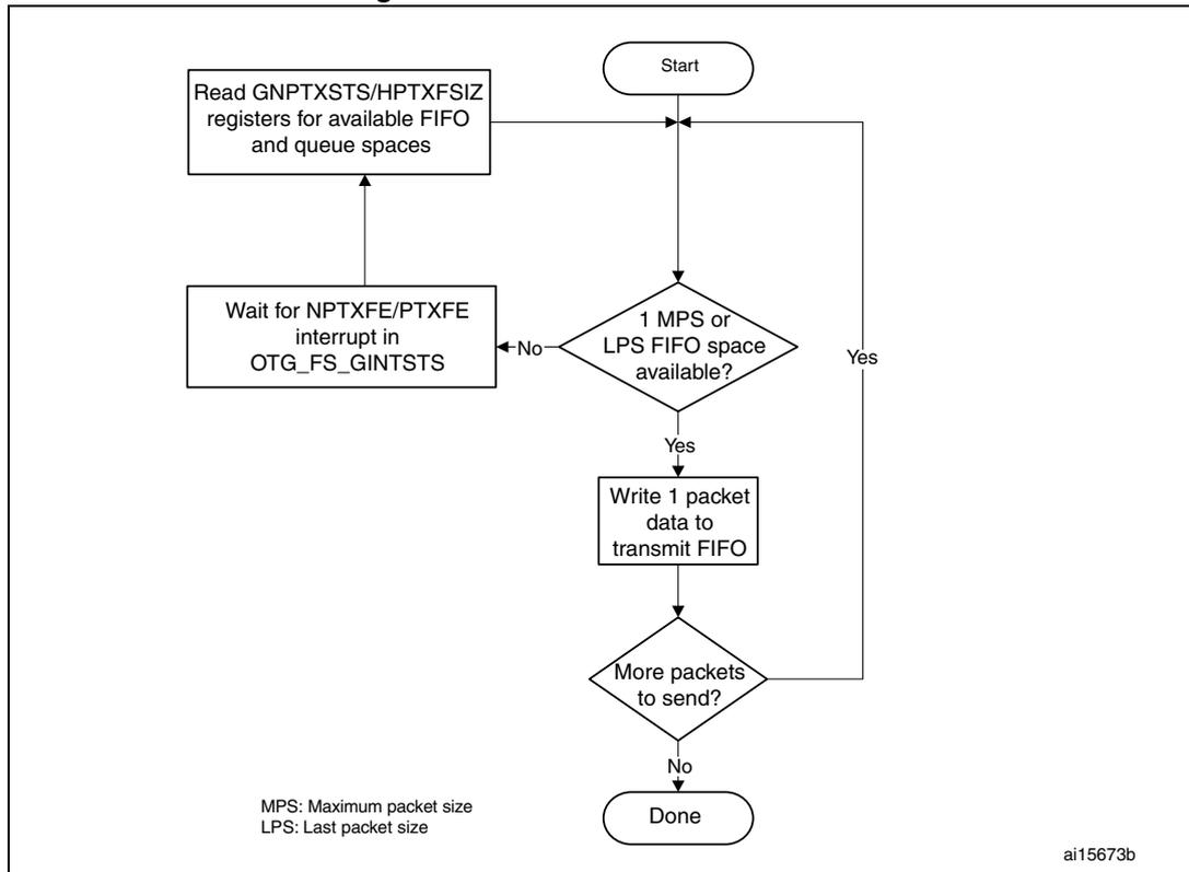
graph TD
    Start([Start]) --> Decision1{1 MPS or
LPS FIFO space
available?}
    Decision1 -- No --> Wait["Wait for NPTXFE/PTXFE
interrupt in
OTG_FS_GINTSTS"]
    Wait --> Read["Read GNPTXSTS/HPTXFSIZ
registers for available FIFO
and queue spaces"]
    Read --> Decision1
    Decision1 -- Yes --> Write["Write 1 packet
data to
transmit FIFO"]
    Write --> Decision2{More packets
to send?}
    Decision2 -- No --> Done([Done])
    Decision2 -- Yes --> Decision1
MPS: Maximum packet size
LPS: Last packet size
ai15673b
- • Reading the receive FIFO
The application must ignore all packet statuses other than IN data packet (bx0010).
Figure 253. Receive FIFO read task
graph TD
    Start([Start]) --> RXFLVL{RXFLVL interrupt?}
    RXFLVL -- No --> RXFLVL
    RXFLVL -- Yes --> Mask[Mask RXFLVL interrupt]
    Mask --> ReadGRXSTSP[Read OTG_FS_GRXSTSP]
    ReadGRXSTSP --> PKTSTS{PKTSTS 0b0010?}
    PKTSTS -- No --> Unmask1[Unmask RXFLVL interrupt]
    PKTSTS -- Yes --> BCNT{BCNT > 0?}
    BCNT -- Yes --> ReadFIFO[Read the received packet from the Receive FIFO]
    ReadFIFO --> Unmask2[Unmask RXFLVL interrupt]
    BCNT -- No --> Unmask3[Unmask RXFLVL interrupt]
    Unmask1 --> RXFLVL
    Unmask2 --> RXFLVL
    Unmask3 --> RXFLVL
- • Bulk and control OUT/SETUP transactions
A typical bulk or control OUT/SETUP pipelined transaction-level operation is shown in Figure 254 . See channel 1 (ch_1). Two bulk OUT packets are transmitted. A control SETUP transaction operates in the same way but has only one packet. The assumptions are:
- – The application is attempting to send two maximum-packet-size packets (transfer size = 1, 024 bytes).
- – The non-periodic transmit FIFO can hold two packets (128 bytes for FS).
- – The non-periodic request queue depth = 4.
- • Normal bulk and control OUT/SETUP operations
The sequence of operations in (channel 1) is as follows:
- a) Initialize channel 1
- b) Write the first packet for channel 1
- c) Along with the last word write, the core writes an entry to the non-periodic request queue
- d) As soon as the non-periodic queue becomes non-empty, the core attempts to send an OUT token in the current frame
- e) Write the second (last) packet for channel 1
- f) The core generates the XFRC interrupt as soon as the last transaction is completed successfully
- g) In response to the XFRC interrupt, de-allocate the channel for other transfers
- h) Handling non-ACK responses
Figure 254. Normal bulk/control OUT/SETUP and bulk/control IN transactions
The diagram illustrates the interaction between an Application, AHB, Host, USB, and Device for normal bulk/control OUT/SETUP and bulk/control IN transactions. The sequence of events is as follows:
- Application
calls
init_reg(ch_1)(1) andwrite_tx_fifo(ch_1)(2) to prepare data for OUT/SETUP. - Application
calls
set_ch_en(ch_2)(5) to enable the channel. - Host (3) initiates the transfer via the USB (4).
- Device receives the data (DATA0 MPS) and responds with ACK.
- Host (3) receives the ACK and then initiates an IN transfer (4).
- Device responds with DATA1 MPS and ACK.
- Host (6) receives the ACK and generates an XFRC interrupt (7).
- Application
calls
De-allocate(ch_1)(7) to free the channel. - Host (8) generates an RXFLVL interrupt (9).
- Application
calls
read_rx_sts(11) andDisable(ch_2)(9) to handle the IN transfer. - Host (10) generates a CHH interrupt (12).
- Application
calls
De-allocate(ch_2)(13) to free the channel.
The USB section includes a Non-Periodic Request Queue (Assume that this queue can hold 4 entries).
The channel-specific interrupt service routine for bulk and control OUT/SETUP transactions is shown in the following code samples.
- • Interrupt service routine for bulk/control OUT/SETUP and bulk/control IN transactions
- a) Bulk/Control OUT/SETUP
Unmask (NAK/TXERR/STALL/XFRC)
if (XFRC)
{
Reset Error Count
Mask ACK
De-allocate Channel
}
else if (STALL)
{
Transfer Done = 1
Unmask CHH
Disable Channel
}
else if (NAK or TXERR )
{
Rewind Buffer Pointers
Unmask CHH
Disable Channel
if (TXERR)
{
Increment Error Count
Unmask ACK
}
else
{
Reset Error Count
}
}
else if (CHH)
{
Mask CHH
if (Transfer Done or (Error_count == 3))
{
De-allocate Channel
}
else
{
Re-initialize Channel
}
}
else if (ACK)
{
Reset Error Count
Mask ACK
}The application is expected to write the data packets into the transmit FIFO as and when the space is available in the transmit FIFO and the Request queue. The application can make use of the NPTXFE interrupt in OTG_FS_GINTSTS to find the transmit FIFO space.
b) Bulk/Control IN
Unmask (TXERR/XFRC/BBERR/STALL/DTERR)
if (XFRC)
{
    Reset Error Count
}
Unmask CHH
Disable Channel
Reset Error Count
Mask ACK
}
else if (TXERR or BBERR or STALL)
{
Unmask CHH
Disable Channel
if (TXERR)
{
Increment Error Count
Unmask ACK
}
}
else if (CHH)
{
Mask CHH
if (Transfer Done or (Error_count == 3))
{
De-allocate Channel
}
else
{
Re-initialize Channel
}
}
else if (ACK)
{
Reset Error Count
Mask ACK
}
else if (DTERR)
{
Reset Error Count
}The application is expected to write the requests as and when the Request queue space is available and until the XFRC interrupt is received.
- • Bulk and control IN transactions
A typical bulk or control IN pipelined transaction-level operation is shown in Figure 255 . See channel 2 (ch_2). The assumptions are:
- – The application is attempting to receive two maximum-packet-size packets (transfer size = 1 024 bytes).
- – The receive FIFO can contain at least one maximum-packet-size packet and two status words per packet (72 bytes for FS).
- – The non-periodic request queue depth = 4.
Figure 255. Bulk/control IN transactions
The diagram illustrates the sequence of operations for Bulk/control IN transactions across five columns: Application, AHB, Host, USB, and Device. The sequence is numbered 1 through 13.
- 1:
Application calls
init_reg(ch_2)andinit_reg(ch_1). - 2:
Application calls
set_ch_en(ch_2)andwrite_tx_fifo(ch_1). - 3:
AHB sends 1 MPS to Host. Host adds
ch_1andch_2to the Non-Periodic Request Queue. - 4: USB sends an OUT token to Device.
- 5:
Application calls
set_ch_en(ch_2)andwrite_tx_fifo(ch_1). AHB sends 1 MPS to Host. Host generates an RXFLVL interrupt. - 6: USB receives DATA0 (1 MPS) from Device and sends an ACK. Host generates an XFRC interrupt.
- 7:
Application calls
read_rx_fifoandset_ch_en(ch_2). AHB receives 1 MPS from Host. - 8: USB sends an IN token to Device. Host generates an RXFLVL interrupt.
- 9:
Application calls
read_rx_fifoandset_ch_en(ch_2). AHB receives 1 MPS from Host. - 10: USB receives DATA1 (1 MPS) from Device and sends an ACK. Host generates an XFRC interrupt.
- 11:
Application calls
read_rx_fifoandset_ch_en(ch_2). AHB receives 1 MPS from Host. - 12: USB sends an IN token to Device. Host generates a CHH interrupt.
- 13:
Application calls
De-allocate(ch_2). Host generates a CHH interrupt.
Non-Periodic Request Queue: Assume that this queue can hold 4 entries.
The sequence of operations is as follows:
- Initialize channel 2.
- Set the CHENA bit in HCCHAR2 to write an IN request to the non-periodic request queue.
- The core attempts to send an IN token after completing the current OUT transaction.
- The core generates an RXFLVL interrupt as soon as the received packet is written to the receive FIFO.
- In response to the RXFLVL interrupt, mask the RXFLVL interrupt and read the received packet status to determine the number of bytes received, then read the receive FIFO accordingly. Following this, unmask the RXFLVL interrupt.
- f) The core generates the RXFLVL interrupt for the transfer completion status entry in the receive FIFO.
- g) The application must read and ignore the receive packet status when the receive packet status is not an IN data packet (PKTSTS in GRXSTSR \( \neq \) 0b0010).
- h) The core generates the XFRC interrupt as soon as the receive packet status is read.
- i) In response to the XFRC interrupt, disable the channel and stop writing the OTG_FS_HCCHAR2 register for further requests. The core writes a channel disable request to the non-periodic request queue as soon as the OTG_FS_HCCHAR2 register is written.
- j) The core generates the RXFLVL interrupt as soon as the halt status is written to the receive FIFO.
- k) Read and ignore the receive packet status.
- l) The core generates a CHH interrupt as soon as the halt status is popped from the receive FIFO.
- m) In response to the CHH interrupt, de-allocate the channel for other transfers.
- n) Handling non-ACK responses
- • Control transactions
Setup, Data, and Status stages of a control transfer must be performed as three separate transfers. Setup-, Data- or Status-stage OUT transactions are performed similarly to the bulk OUT transactions explained previously. Data- or Status-stage IN transactions are performed similarly to the bulk IN transactions explained previously. For all three stages, the application is expected to set the EPTYP field in OTG_FS_HCCHAR1 to Control. During the Setup stage, the application is expected to set the PID field in OTG_FS_HCTSIZ1 to SETUP.
- • Interrupt OUT transactions
A typical interrupt OUT operation is shown in Figure 256 . The assumptions are:
- – The application is attempting to send one packet in every frame (up to 1 maximum packet size), starting with the odd frame (transfer size = 1 024 bytes)
- – The periodic transmit FIFO can hold one packet (1 KB)
- – Periodic request queue depth = 4
The sequence of operations is as follows:
- a) Initialize and enable channel 1. The application must set the ODDFRM bit in OTG_FS_HCCHAR1.
- b) Write the first packet for channel 1.
- c) Along with the last word write of each packet, the OTG_FS host writes an entry to the periodic request queue.
- d) The OTG_FS host attempts to send an OUT token in the next (odd) frame.
- e) The OTG_FS host generates an XFRC interrupt as soon as the last packet is transmitted successfully.
- f) In response to the XFRC interrupt, reinitialize the channel for the next transfer.
Figure 256. Normal interrupt OUT/IN transactions
The diagram illustrates the interaction between an Application, AHB, Host, USB, and Device over two micro-frames (Odd and Even).
Odd (micro) frame:
1. Application initializes channel 2 (
init_reg(ch_2)
) and channel 1 (
init_reg(ch_1)
).
2. Application enables channel 2 (
set_ch_en(ch_2)
) and writes to TX FIFO for channel 1 (
write_tx_fifo(ch_1)
).
3. AHB transfers 1 MPS to the Host, which places ch_1 and ch_2 in the Periodic Request Queue.
4. USB performs an OUT transaction with DATA0 and MPS to the Device.
5. Device responds with ACK. Host generates XFRC interrupt.
6. Application reads RX status and FIFO (
read_rx_sts
,
read_rx_fifo
) after RXFLVL interrupt.
Even (micro) frame:
7. Application reads RX status.
8. Host generates XFRC interrupt for channel 1.
9. Application re-initializes and enables channel 2.
Transactions continue with DATA1 in the Even frame.
ai15676
- • Interrupt service routine for interrupt OUT/IN transactions
a) Interrupt OUT
Unmask (NAK/TXERR/STALL/XFRC/FRMOR)
if (XFRC)
{
    Reset Error Count
    Mask ACK
    De-allocate Channel
}
else
    if (STALL or FRMOR)
    {
        Mask ACK
        Unmask CHH
    }
Disable Channel
if (STALL)
{
Transfer Done = 1
}
}
else
if (NAK or TXERR)
{
Rewind Buffer Pointers
Reset Error Count
Mask ACK
Unmask CHH
Disable Channel
}
else
if (CHH)
{
Mask CHH
if (Transfer Done or (Error_count == 3))
{
De-allocate Channel
}
else
{
Re-initialize Channel (in next b_interval - 1 Frame)
}
}
else
if (ACK)
{
Reset Error Count
Mask ACK
}The application uses the NPTXFE interrupt in OTG_FS_GINTSTS to find the transmit FIFO space.
b) Interrupt IN
Unmask (NAK/TXERR/XFRC/BBERR/STALL/FRMOR/DTERR)
if (XFRC)
{
    Reset Error Count
    Mask ACK
    if (OTG_FS_HCTSIZx.PKTCNT == 0)
    {
        De-allocate Channel
    }
    else
    {
        Transfer Done = 1
        Unmask CHH
        Disable Channel
    }
}
}
}
else
if (STALL or FRMOR or NAK or DTERR or BBERR)
{
Mask ACK
Unmask CHH
Disable Channel
if (STALL or BBERR)
{
Reset Error Count
Transfer Done = 1
}
else
if (!FRMOR)
{
Reset Error Count
}
}
else
if (TXERR)
{
Increment Error Count
Unmask ACK
Unmask CHH
Disable Channel
}
else
if (CHH)
{
Mask CHH
if (Transfer Done or (Error_count == 3))
{
De-allocate Channel
}
else
Re-initialize Channel (in next b_interval - 1 /Frame)
}
}
else
if (ACK)
{
Reset Error Count
Mask ACK
}
}
- • Interrupt IN transactions
The assumptions are:
- – The application is attempting to receive one packet (up to 1 maximum packet size) in every frame, starting with odd (transfer size = 1 024 bytes).
- – The receive FIFO can hold at least one maximum-packet-size packet and two status words per packet (1 031 bytes).
- – Periodic request queue depth = 4.
- • Normal interrupt IN operation
The sequence of operations is as follows:
- a) Initialize channel 2. The application must set the ODDFRM bit in OTG_FS_HCCHAR2.
- b) Set the CHENA bit in OTG_FS_HCCHAR2 to write an IN request to the periodic request queue.
- c) The OTG_FS host writes an IN request to the periodic request queue for each OTG_FS_HCCHAR2 register write with the CHENA bit set.
- d) The OTG_FS host attempts to send an IN token in the next (odd) frame.
- e) As soon as the IN packet is received and written to the receive FIFO, the OTG_FS host generates an RXFLVL interrupt.
- f) In response to the RXFLVL interrupt, read the received packet status to determine the number of bytes received, then read the receive FIFO accordingly. The application must mask the RXFLVL interrupt before reading the receive FIFO, and unmask after reading the entire packet.
- g) The core generates the RXFLVL interrupt for the transfer completion status entry in the receive FIFO. The application must read and ignore the receive packet status when the receive packet status is not an IN data packet (PKTSTS in GRXSTSR ≠ 0b0010).
- h) The core generates an XFRC interrupt as soon as the receive packet status is read.
- i) In response to the XFRC interrupt, read the PKTCNT field in OTG_FS_HCTSIZ2. If the PKTCNT bit in OTG_FS_HCTSIZ2 is not equal to 0, disable the channel before re-initializing the channel for the next transfer, if any). If PKTCNT bit in
OTG_FS_HCTSIZ2 = 0, reinitialize the channel for the next transfer. This time, the application must reset the ODDFRM bit in OTG_FS_HCCHAR2.
- • Isochronous OUT transactions
A typical isochronous OUT operation is shown in Figure 257 . The assumptions are:
- – The application is attempting to send one packet every frame (up to 1 maximum packet size), starting with an odd frame. (transfer size = 1 024 bytes).
- – The periodic transmit FIFO can hold one packet (1 KB).
- – Periodic request queue depth = 4.
The sequence of operations is as follows:
- a) Initialize and enable channel 1. The application must set the ODDFRM bit in OTG_FS_HCCHAR1.
- b) Write the first packet for channel 1.
- c) Along with the last word write of each packet, the OTG_FS host writes an entry to the periodic request queue.
- d) The OTG_FS host attempts to send the OUT token in the next frame (odd).
- e) The OTG_FS host generates the XFRC interrupt as soon as the last packet is transmitted successfully.
- f) In response to the XFRC interrupt, reinitialize the channel for the next transfer.
- g) Handling non-ACK responses
Figure 257. Normal isochronous OUT/IN transactions
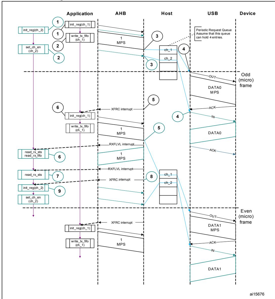
The diagram illustrates the interaction for isochronous transactions. It is divided into two main sections: 'Odd (micro) frame' and 'Even (micro) frame', separated by a dashed line.
In the 'Odd (micro) frame':
1. The Application initializes channel 2 (
init_reg(ch_2)
) and channel 1 (
init_reg(ch_1)
).
2. The Application writes to the TX FIFO for channel 1 (
write_tx_fifo(ch_1)
) and enables channel 2 (
set_ch_en(ch_2)
).
3. The AHB transfers 1 MPS (Maximum Packet Size) to the Host for channel 1.
4. The Host schedules the transactions in the 'Periodic Request Queue' (containing
ch_1
and
ch_2
).
5. The USB performs an OUT transaction:
OUT
packet followed by
DATA0
(1 MPS) and an
ACK
from the device.
6. An
XFRC
(Transfer Complete) interrupt is generated for channel 1. The Application reads receive status and FIFO (
read_rx_sts
,
read_rx_fifo
).
7. An
RXFLVL
(Receive FIFO Level) interrupt is generated. The Application reads receive status again.
8. The Host processes channel 1 and channel 2 in its internal queue.
9. An
XFRC
interrupt is generated for channel 2. The Application re-initializes and enables channel 2 for the next frame.
In the 'Even (micro) frame':
- The process repeats with
DATA1
payloads for both OUT and IN transactions, showing the toggle between DATA0 and DATA1 in successive frames.
- • Interrupt service routine for isochronous OUT/IN transactions
Code sample: Isochronous OUT
Unmask (FRMOR/XFRC)
if (XFRC)
{
    De-allocate Channel
}
else
    if (FRMOR)
    {
        Unmask CHH
        Disable Channel
    }
else
if (CHH)
{
Mask CHH
De-allocate Channel
}
Code sample: Isochronous IN
Unmask (TXERR/XFRC/FRMOR/BBERR)
if (XFRC or FRMOR)
{
if (XFRC and (OTG_FS_HCTSIZx.PKTCNT == 0))
{
Reset Error Count
De-allocate Channel
}
else
{
Unmask CHH
Disable Channel
}
}
else
if (TXERR or BBERR)
{
Increment Error Count
Unmask CHH
Disable Channel
}
else
if (CHH)
{
Mask CHH
if (Transfer Done or (Error_count == 3))
{
De-allocate Channel
}
else
{
Re-initialize Channel
}
}- • Isochronous IN transactions
The assumptions are:
- – The application is attempting to receive one packet (up to 1 maximum packet size) in every frame starting with the next odd frame (transfer size = 1 024 bytes).
- – The receive FIFO can hold at least one maximum-packet-size packet and two status word per packet (1 031 bytes).
- – Periodic request queue depth = 4.
The sequence of operations is as follows:
- Initialize channel 2. The application must set the ODDFRM bit in OTG_FS_HCCHAR2.
- Set the CHENA bit in OTG_FS_HCCHAR2 to write an IN request to the periodic request queue.
- The OTG_FS host writes an IN request to the periodic request queue for each OTG_FS_HCCHAR2 register write with the CHENA bit set.
- The OTG_FS host attempts to send an IN token in the next odd frame.
- As soon as the IN packet is received and written to the receive FIFO, the OTG_FS host generates an RXFLVL interrupt.
- In response to the RXFLVL interrupt, read the received packet status to determine the number of bytes received, then read the receive FIFO accordingly. The application must mask the RXFLVL interrupt before reading the receive FIFO, and unmask it after reading the entire packet.
- The core generates an RXFLVL interrupt for the transfer completion status entry in the receive FIFO. This time, the application must read and ignore the receive packet status when the receive packet status is not an IN data packet (PKTSTS bit in OTG_FS_GRXSTSR ≠ 0b0010).
- The core generates an XFRC interrupt as soon as the receive packet status is read.
- In response to the XFRC interrupt, read the PKTCNT field in OTG_FS_HCTSIZ2. If PKTCNT ≠ 0 in OTG_FS_HCTSIZ2, disable the channel before re-initializing the channel for the next transfer, if any. If PKTCNT = 0 in OTG_FS_HCTSIZ2, reinitialize the channel for the next transfer. This time, the application must reset the ODDFRM bit in OTG_FS_HCCHAR2.
- • Selecting the queue depth
Choose the periodic and non-periodic request queue depths carefully to match the number of periodic/non-periodic endpoints accessed.
The non-periodic request queue depth affects the performance of non-periodic transfers. The deeper the queue (along with sufficient FIFO size), the more often the core is able to pipeline non-periodic transfers. If the queue size is small, the core is able to put in new requests only when the queue space is freed up.
The core's periodic request queue depth is critical to perform periodic transfers as scheduled. Select the periodic queue depth, based on the number of periodic transfers scheduled in a microframe. If the periodic request queue depth is smaller than the periodic transfers scheduled in a microframe, a frame overrun condition occurs.
- • Handling babble conditions
OTG_FS controller handles two cases of babble: packet babble and port babble. Packet babble occurs if the device sends more data than the maximum packet size for
the channel. Port babble occurs if the core continues to receive data from the device at EOF2 (the end of frame 2, which is very close to SOF).
When OTG_FS controller detects a packet babble, it stops writing data into the Rx buffer and waits for the end of packet (EOP). When it detects an EOP, it flushes already written data in the Rx buffer and generates a Babble interrupt to the application.
When OTG_FS controller detects a port babble, it flushes the RxFIFO and disables the port. The core then generates a Port disabled interrupt (HPRTINT in OTG_FS_GINTSTS, PENCHNG in OTG_FS_HPRT). On receiving this interrupt, the application must determine that this is not due to an overcurrent condition (another cause of the Port Disabled interrupt) by checking POCA in OTG_FS_HPRT, then perform a soft reset. The core does not send any more tokens after it has detected a port babble condition.
22.17.5 Device programming model
Endpoint initialization on USB reset
- 1. Set the NAK bit for all OUT endpoints
- – SNAK = 1 in OTG_FS_DOEPCTLx (for all OUT endpoints)
- 2. Unmask the following interrupt bits
- – INEP0 = 1 in OTG_FS_DAINTEMSK (control 0 IN endpoint)
- – OUTEP0 = 1 in OTG_FS_DAINTEMSK (control 0 OUT endpoint)
- – STUP = 1 in DOEPEMSK
- – XFRC = 1 in DOEPEMSK
- – XFRC = 1 in DIEPEMSK
- – TOC = 1 in DIEPEMSK
- 3. Set up the Data FIFO RAM for each of the FIFOs
- – Program the OTG_FS_GRXFSIZ register, to be able to receive control OUT data and setup data. If thresholding is not enabled, at a minimum, this must be equal to 1 max packet size of control endpoint 0 + 2 words (for the status of the control OUT data packet) + 10 words (for setup packets).
- – Program the OTG_FS_TX0FSIZ register (depending on the FIFO number chosen) to be able to transmit control IN data. At a minimum, this must be equal to 1 max packet size of control endpoint 0.
- 4. Program the following fields in the endpoint-specific registers for control OUT endpoint 0 to receive a SETUP packet
- – STUPCNT = 3 in OTG_FS_DOEPTSIZ0 (to receive up to 3 back-to-back SETUP packets)
At this point, all initialization required to receive SETUP packets is done.
Endpoint initialization on enumeration completion
- 1. On the Enumeration Done interrupt (ENUMDNE in OTG_FS_GINTSTS), read the OTG_FS_DSTS register to determine the enumeration speed.
- 2. Program the MPSIZ field in OTG_FS_DIEPCTL0 to set the maximum packet size. This step configures control endpoint 0. The maximum packet size for a control endpoint depends on the enumeration speed.
At this point, the device is ready to receive SOF packets and is configured to perform control transfers on control endpoint 0.
Endpoint initialization on SetAddress command
This section describes what the application must do when it receives a SetAddress command in a SETUP packet.
- 1. Program the OTG_FS_DCFG register with the device address received in the SetAddress command
- 2. Program the core to send out a status IN packet
Endpoint initialization on SetConfiguration/SetInterface command
This section describes what the application must do when it receives a SetConfiguration or SetInterface command in a SETUP packet.
- 1. When a SetConfiguration command is received, the application must program the endpoint registers to configure them with the characteristics of the valid endpoints in the new configuration.
- 2. When a SetInterface command is received, the application must program the endpoint registers of the endpoints affected by this command.
- 3. Some endpoints that were active in the prior configuration or alternate setting are not valid in the new configuration or alternate setting. These invalid endpoints must be deactivated.
- 4. Unmask the interrupt for each active endpoint and mask the interrupts for all inactive endpoints in the OTG_FS_DAINTRMSK register.
- 5. Set up the Data FIFO RAM for each FIFO.
- 6. After all required endpoints are configured; the application must program the core to send a status IN packet.
At this point, the device core is configured to receive and transmit any type of data packet.
Endpoint activation
This section describes the steps required to activate a device endpoint or to configure an existing device endpoint to a new type.
- 1. Program the characteristics of the required endpoint into the following fields of the OTG_FS_DIEPCTLx register (for IN or bidirectional endpoints) or the OTG_FS_DOEPCTLx register (for OUT or bidirectional endpoints).
- – Maximum packet size
- – USB active endpoint = 1
- – Endpoint start data toggle (for interrupt and bulk endpoints)
- – Endpoint type
- – TxFIFO number
- 2. Once the endpoint is activated, the core starts decoding the tokens addressed to that endpoint and sends out a valid handshake for each valid token received for the endpoint.
Endpoint deactivation
This section describes the steps required to deactivate an existing endpoint.
- 1. In the endpoint to be deactivated, clear the USB active endpoint bit in the OTG_FS_DIEPCTLx register (for IN or bidirectional endpoints) or the OTG_FS_DOEPCTLx register (for OUT or bidirectional endpoints).
- 2. Once the endpoint is deactivated, the core ignores tokens addressed to that endpoint, which results in a timeout on the USB.
Note:
The application must meet the following conditions to set up the device core to handle traffic:
NPTXFEM and RXFLVLM in the OTG_FS_GINTMSK register must be cleared.
22.17.6 Operational model
SETUP and OUT data transfers
This section describes the internal data flow and application-level operations during data OUT transfers and SETUP transactions.
- • Packet read
This section describes how to read packets (OUT data and SETUP packets) from the receive FIFO.
- 1. On catching an RXFLVL interrupt (OTG_FS_GINTSTS register), the application must read the Receive status pop register (OTG_FS_GRXSTSP).
- 2. The application can mask the RXFLVL interrupt (in OTG_FS_GINTSTS) by writing to RXFLVL = 0 (in OTG_FS_GINTMSK), until it has read the packet from the receive FIFO.
- 3. If the received packet's byte count is not 0, the byte count amount of data is popped from the receive Data FIFO and stored in memory. If the received packet byte count is 0, no data is popped from the receive data FIFO.
- 4. The receive FIFO's packet status readout indicates one of the following:
- a) Global OUT NAK pattern:
PKTSTS = Global OUT NAK, BCNT = 0x000, EPNUM = Don't Care (0x0),
DPID = Don't Care (0b00).
These data indicate that the global OUT NAK bit has taken effect. - b) SETUP packet pattern:
PKTSTS = SETUP, BCNT = 0x008, EPNUM = Control EP Num, DPID = D0.
These data indicate that a SETUP packet for the specified endpoint is now available for reading from the receive FIFO. - c) Setup stage done pattern:
PKTSTS = Setup Stage Done, BCNT = 0x0, EPNUM = Control EP Num,
DPID = Don't Care (0b00).
These data indicate that the Setup stage for the specified endpoint has completed and the Data stage has started. After this entry is popped from the receive FIFO, the core asserts a Setup interrupt on the specified control OUT endpoint. - d) Data OUT packet pattern:
PKTSTS = DataOUT, BCNT = size of the received data OUT packet (0 ≤ BCNT ≤ 1 024), EPNUM = EPNUM on which the packet was received, DPID = Actual Data PID.
- a) Global OUT NAK pattern:
- e) Data transfer completed pattern:
PKTSTS = Data OUT Transfer Done, BCNT = 0x0, EPNUM = OUT EP Num on which the data transfer is complete, DPID = Don't Care (0b00). These data indicate that an OUT data transfer for the specified OUT endpoint has completed. After this entry is popped from the receive FIFO, the core asserts a Transfer Completed interrupt on the specified OUT endpoint. - 5. After the data payload is popped from the receive FIFO, the RXFLVL interrupt (OTG_FS_GINTSTS) must be unmasked.
- 6. Steps 1–5 are repeated every time the application detects assertion of the interrupt line due to RXFLVL in OTG_FS_GINTSTS. Reading an empty receive FIFO can result in undefined core behavior.
Figure 258 provides a flowchart of the above procedure.
Figure 258. Receive FIFO packet read
![Flowchart of the Receive FIFO packet read procedure. The process starts with 'wait until RXFLVL in OTG_FS_GINTSTSG', followed by 'rd_data = rd_reg (OTG_FS_GRXSTSP);'. A decision diamond 'rd_data.BCNT = 0?' follows. If 'Y' (Yes), it loops back to the start. If 'N' (No), it proceeds to a block 'mem[0: word_cnt - 1] = rd_rxfifo(rd_data.EPNUM, word_cnt)'. This block is associated with 'packet store in memory' and 'word_cnt = BCNT[11:2] + (BCNT[1] | BCNT[1])'. A bracket on the right groups the decision and the memory store block as 'rcv_out_pkt()'. The diagram is labeled 'ai15677b'.](/RM0368-STM32F401xB-C-401xD-E/19c3c1c71e1065f6715b686e45f47fea_img.jpg)
graph TD
    Start(( )) --> Wait[wait until RXFLVL in OTG_FS_GINTSTSG]
    Wait --> RdData[rd_data = rd_reg (OTG_FS_GRXSTSP);]
    RdData --> Decision{rd_data.BCNT = 0?}
    Decision -- Y --> Start
    Decision -- N --> MemStore["mem[0: word_cnt - 1] = rd_rxfifo(rd_data.EPNUM, word_cnt)"]
    MemStore --> WordCnt["word_cnt = BCNT[11:2] + (BCNT[1] | BCNT[1])"]
    WordCnt --> MemStore
    subgraph rcv_out_pkt
        Decision
        MemStore
        WordCnt
    end
    MemStore -.-> PacketStore[packet store in memory]
    ai15677b[ai15677b]
- • SETUP transactions
This section describes how the core handles SETUP packets and the application's sequence for handling SETUP transactions.
- • Application requirements
- 1. To receive a SETUP packet, the STUPCNT field (OTG_FS_DOEPTSIZx) in a control OUT endpoint must be programmed to a non-zero value. When the application programs the STUPCNT field to a non-zero value, the core receives SETUP packets and writes them to the receive FIFO, irrespective of the NAK status and EPENA bit setting in OTG_FS_DOEPCTLx. The STUPCNT field is decremented every time the control endpoint receives a SETUP packet. If the STUPCNT field is not programmed to a proper value before receiving a SETUP packet, the core still receives the SETUP packet and decrements the STUPCNT field, but the application may not be able to
determine the correct number of SETUP packets received in the Setup stage of a control transfer.
- – STUPCNT = 3 in OTG_FS_DOEPTSIZx
- 2. The application must always allocate some extra space in the Receive data FIFO, to be able to receive up to three SETUP packets on a control endpoint.
- – The space to be reserved is 10 words. Three words are required for the first SETUP packet, 1 word is required for the Setup stage done word and 6 words are required to store two extra SETUP packets among all control endpoints.
- – 3 words per SETUP packet are required to store 8 bytes of SETUP data and 4 bytes of SETUP status (Setup packet pattern). The core reserves this space in the receive data FIFO to write SETUP data only, and never uses this space for data packets.
- 3. The application must read the 2 words of the SETUP packet from the receive FIFO.
- 4. The application must read and discard the Setup stage done word from the receive FIFO.
- 2. The application must always allocate some extra space in the Receive data FIFO, to be able to receive up to three SETUP packets on a control endpoint.
- • Internal data flow
- 1. When a SETUP packet is received, the core writes the received data to the receive FIFO, without checking for available space in the receive FIFO and irrespective of the endpoint's NAK and STALL bit settings.
- – The core internally sets the IN NAK and OUT NAK bits for the control IN/OUT endpoints on which the SETUP packet was received.
- 2. For every SETUP packet received on the USB, 3 words of data are written to the receive FIFO, and the STUPCNT field is decremented by 1.
- – The first word contains control information used internally by the core
- – The second word contains the first 4 bytes of the SETUP command
- – The third word contains the last 4 bytes of the SETUP command
- 3. When the Setup stage changes to a Data IN/OUT stage, the core writes an entry (Setup stage done word) to the receive FIFO, indicating the completion of the Setup stage.
- 4. On the AHB side, SETUP packets are emptied by the application.
- 5. When the application pops the Setup stage done word from the receive FIFO, the core interrupts the application with an STUP interrupt (OTG_FS_DOEPINTx), indicating it can process the received SETUP packet.
- – The core clears the endpoint enable bit for control OUT endpoints.
- • Application programming sequence
- 1. Program the OTG_FS_DOEPTSIZx register.
- – STUPCNT = 3
- 2. Wait for the RXFLVL interrupt (OTG_FS_GINTSTS) and empty the data packets from the receive FIFO.
- 3. Assertion of the STUP interrupt (OTG_FS_DOEPINTx) marks a successful completion of the SETUP Data Transfer.
- – On this interrupt, the application must read the OTG_FS_DOEPTSIZx register to determine the number of SETUP packets received and process the last received SETUP packet.
Figure 259. Processing a SETUP packet
![Flowchart illustrating the processing of a SETUP packet. The steps are: Wait for STUP in OTG_FS_DOEPINTx, rem_supcnt = rd_reg(DOEPTSIZx), setup_cmd[31:0] = mem[4 - 2 * rem_supcnt], setup_cmd[63:32] = mem[5 - 2 * rem_supcnt], Find setup cmd type, ctrl-rd/wr/2 stage. The decision leads to Read (setup_np_in_pkt Data IN phase), 2-stage (setup_np_in_pkt Status IN phase), or Write (rcv_out_pkt Data OUT phase).](/RM0368-STM32F401xB-C-401xD-E/75d2f951ce2fea7acc2db181d7a641e6_img.jpg)
graph TD
    A[Wait for STUP in OTG_FS_DOEPINTx] --> B[rem_supcnt = rd_reg(DOEPTSIZx)]
    B --> C["setup_cmd[31:0] = mem[4 - 2 * rem_supcnt]
setup_cmd[63:32] = mem[5 - 2 * rem_supcnt]"]
    C --> D[Find setup cmd type]
    D --> E{ctrl-rd/wr/2 stage}
    E -- Read --> F["setup_np_in_pkt
Data IN phase"]
    E -- 2-stage --> G["setup_np_in_pkt
Status IN phase"]
    E -- Write --> H["rcv_out_pkt
Data OUT phase"]
ai15678
- • Handling more than three back-to-back SETUP packets
Per the USB 2.0 specification, normally, during a SETUP packet error, a host does not send more than three back-to-back SETUP packets to the same endpoint. However, the USB 2.0 specification does not limit the number of back-to-back SETUP packets a host can send to the same endpoint. When this condition occurs, the OTG_FS controller generates an interrupt (B2BSTUP in OTG_FS_DOEPINTx).
- • Setting the global OUT NAK
Internal data flow
- 1. When the application sets the Global OUT NAK (SGONAK bit in OTG_FS_DCTL), the core stops writing data, except SETUP packets, to the receive FIFO. Irrespective of the space availability in the receive FIFO, non-isochronous OUT tokens receive a NAK handshake response, and the core ignores isochronous OUT data packets
- 2. The core writes the Global OUT NAK pattern to the receive FIFO. The application must reserve enough receive FIFO space to write this data pattern.
- 3. When the application pops the Global OUT NAK pattern word from the receive FIFO, the core sets the GONAKEFF interrupt (OTG_FS_GINTSTS).
- 4. Once the application detects this interrupt, it can assume that the core is in Global OUT NAK mode. The application can clear this interrupt by clearing the SGONAK bit in OTG_FS_DCTL.
- 1. To stop receiving any kind of data in the receive FIFO, the application must set the Global OUT NAK bit by programming the following field:
- – SGONAK = 1 in OTG_FS_DCTL
- 2. Wait for the assertion of the GONAKEFF interrupt in OTG_FS_GINTSTS. When asserted, this interrupt indicates that the core has stopped receiving any type of data except SETUP packets.
- 3. The application can receive valid OUT packets after it has set SGONAK in OTG_FS_DCTL and before the core asserts the GONAKEFF interrupt (OTG_FS_GINTSTS).
- 4. The application can temporarily mask this interrupt by writing to the GINAKEFFM bit in the OTG_FS_GINTMSK register.
- – GINAKEFFM = 0 in the OTG_FS_GINTMSK register
- 5. Whenever the application is ready to exit the Global OUT NAK mode, it must clear the SGONAK bit in OTG_FS_DCTL. This also clears the GONAKEFF interrupt (OTG_FS_GINTSTS).
- – OTG_FS_DCTL = 1 in CGONAK
- 6. If the application has masked this interrupt earlier, it must be unmasked as follows:
- – GINAKEFFM = 1 in GINTMSK
- 1. To stop receiving any kind of data in the receive FIFO, the application must set the Global OUT NAK bit by programming the following field:
- • Disabling an OUT endpoint
The application must use this sequence to disable an OUT endpoint that it has enabled.
Application programming sequence- 1. Before disabling any OUT endpoint, the application must enable Global OUT NAK mode in the core.
- – SGONAK = 1 in OTG_FS_DCTL
- 2. Wait for the GONAKEFF interrupt (OTG_FS_GINTSTS)
- 3. Disable the required OUT endpoint by programming the following fields:
- – EPDIS = 1 in OTG_FS_DOEPCTLx
- – SNAK = 1 in OTG_FS_DOEPCTLx
- 4. Wait for the EPDISD interrupt (OTG_FS_DOEPINTx), which indicates that the OUT endpoint is completely disabled. When the EPDISD interrupt is asserted, the core also clears the following bits:
- – EPDIS = 0 in OTG_FS_DOEPCTLx
- – EPENA = 0 in OTG_FS_DOEPCTLx
- 5. The application must clear the Global OUT NAK bit to start receiving data from other non-disabled OUT endpoints.
- – SGONAK = 0 in OTG_FS_DCTL
- 1. Before disabling any OUT endpoint, the application must enable Global OUT NAK mode in the core.
- • Transfer Stop Programming for OUT endpoints
The application must use the following programming sequence to stop any transfers (because of an interrupt from the host, typically a reset).
Sequence of operations:
- 1. Enable all OUT endpoints by setting
- – EPENA = 1 in all OTG_FS_DOEPCTLx registers.
- 2. Flush the RxFIFO as follows
- – Poll OTG_FS_GRSTCTL.AHBIDL until it is 1. This indicates that AHB master is idle.
- – Perform read modify write operation on OTG_FS_GRSTCTL.RXFFLSH = 1
- – Poll OTG_FS_GRSTCTL.RXFFLSH until it is 0, but also using a timeout of less than 10 milli-seconds (corresponds to minimum reset signaling duration). If 0 is seen before the timeout, then the RxFIFO flush is successful. If at the moment the timeout occurs, there is still a 1, (this may be due to a packet on EP0 coming from the host) then go back (once only) to the previous step (“Perform read modify write operation”).
- 3. Before disabling any OUT endpoint, the application must enable Global OUT NAK mode in the core, according to the instructions in “ Setting the global OUT NAK on page 787 ”. This ensures that data in the RxFIFO is sent to the application successfully. Set SGONAK = 1 in OTG_FS_DCTL
- 4. Wait for the GONAKEFF interrupt (OTG_FS_GINTSTS)
- 5. Disable all active OUT endpoints by programming the following register bits:
- – EPDIS = 1 in registers OTG_FS_DOEPCTLx
- – SNAK = 1 in registers OTG_FS_DOEPCTLx
- 6. Wait for the EPDIS interrupt in OTG_FS_DOEPINTx for each OUT endpoint programmed in the previous step. The EPDIS interrupt in OTG_FS_DOEPINTx indicates that the corresponding OUT endpoint is completely disabled. When the EPDIS interrupt is asserted, the following bits are cleared:
- – EPENA = 0 in registers OTG_FS_DOEPCTLx
- – EPDIS = 0 in registers OTG_FS_DOEPCTLx
- – SNAK = 0 in registers OTG_FS_DOEPCTLx
- 1. Enable all OUT endpoints by setting
- • Generic non-isochronous OUT data transfers
This section describes a regular non-isochronous OUT data transfer (control, bulk, or interrupt).
Application requirements
- 1. Before setting up an OUT transfer, the application must allocate a buffer in the memory to accommodate all data to be received as part of the OUT transfer.
- 2. For OUT transfers, the transfer size field in the endpoint's transfer size register must be a multiple of the maximum packet size of the endpoint, adjusted to the word boundary.
- – transfer size[EPNUM] = \( n \times (\text{MPSIZ[EPNUM]} + 4 - (\text{MPSIZ[EPNUM]} \bmod 4)) \)
- – packet count[EPNUM] = \( n \)
- – \( n > 0 \)
- 3. On any OUT endpoint interrupt, the application must read the endpoint's transfer size register to calculate the size of the payload in the memory. The received payload size can be less than the programmed transfer size.
- – Payload size in memory = application programmed initial transfer size – core updated final transfer size
- – Number of USB packets in which this payload was received = application programmed initial packet count – core updated final packet count
Internal data flow
- 1. The application must set the transfer size and packet count fields in the endpoint-specific registers, clear the NAK bit, and enable the endpoint to receive the data.
- 2. Once the NAK bit is cleared, the core starts receiving data and writes it to the receive FIFO, as long as there is space in the receive FIFO. For every data packet received on the USB, the data packet and its status are written to the receive FIFO. Every packet (maximum packet size or short packet) written to the receive FIFO decrements the packet count field for that endpoint by 1.
- – OUT data packets received with bad data CRC are flushed from the receive FIFO automatically.
- – After sending an ACK for the packet on the USB, the core discards non-isochronous OUT data packets that the host, which cannot detect the ACK, re-sends. The application does not detect multiple back-to-back data OUT packets on the same endpoint with the same data PID. In this case the packet count is not decremented.
- – If there is no space in the receive FIFO, isochronous or non-isochronous data packets are ignored and not written to the receive FIFO. Additionally, non-isochronous OUT tokens receive a NAK handshake reply.
- – In all the above three cases, the packet count is not decremented because no data are written to the receive FIFO.
- 3. When the packet count becomes 0 or when a short packet is received on the endpoint, the NAK bit for that endpoint is set. Once the NAK bit is set, the isochronous or non-isochronous data packets are ignored and not written to the receive FIFO, and non-isochronous OUT tokens receive a NAK handshake reply.
- 4. After the data are written to the receive FIFO, the application reads the data from the receive FIFO and writes it to external memory, one packet at a time per endpoint.
- 5. At the end of every packet write on the AHB to external memory, the transfer size for the endpoint is decremented by the size of the written packet.
- 6. The OUT data transfer completed pattern for an OUT endpoint is written to the receive FIFO on one of the following conditions:
- – The transfer size is 0 and the packet count is 0
- – The last OUT data packet written to the receive FIFO is a short packet ( \( 0 \leq \text{packet size} < \text{maximum packet size} \) )
- 7. When either the application pops this entry (OUT data transfer completed), a transfer completed interrupt is generated for the endpoint and the endpoint enable is cleared.
Application programming sequence
- 1. Program the OTG_FS_DOEPTSIZx register for the transfer size and the corresponding packet count.
- 2. Program the OTG_FS_DOEPCTLx register with the endpoint characteristics, and set the EPENA and CNAK bits.
- – EPENA = 1 in OTG_FS_DOEPCTLx
- – CNAK = 1 in OTG_FS_DOEPCTLx
- 3. Wait for the RXFLVL interrupt (in OTG_FS_GINTSTS) and empty the data packets from the receive FIFO.
- – This step can be repeated many times, depending on the transfer size.
- 4. Asserting the XFRC interrupt (OTG_FS_DOEPINTx) marks a successful completion of the non-isochronous OUT data transfer.
- 5. Read the OTG_FS_DOEPTSIZx register to determine the size of the received data payload.
- • Generic isochronous OUT data transfer
This section describes a regular isochronous OUT data transfer.
Application requirements
- 1. All the application requirements for non-isochronous OUT data transfers also apply to isochronous OUT data transfers.
- 2. For isochronous OUT data transfers, the transfer size and packet count fields must always be set to the number of maximum-packet-size packets that can be received in a single frame and no more. Isochronous OUT data transfers cannot span more than 1 frame.
- 3. The application must read all isochronous OUT data packets from the receive FIFO (data and status) before the end of the periodic frame (EOPF interrupt in OTG_FS_GINTSTS).
- 4. To receive data in the following frame, an isochronous OUT endpoint must be enabled after the EOPF (OTG_FS_GINTSTS) and before the SOF (OTG_FS_GINTSTS).
Internal data flow
- 1. The internal data flow for isochronous OUT endpoints is the same as that for non-isochronous OUT endpoints, but for a few differences.
- 2. When an isochronous OUT endpoint is enabled by setting the Endpoint Enable and clearing the NAK bits, the Even/Odd frame bit must also be set appropriately. The core receives data on an isochronous OUT endpoint in a particular frame only if the following condition is met:
- – EONUM (in OTG_FS_DOEPCTLx) = SOFFN[0] (in OTG_FS_DSTS)
- 3. When the application completely reads an isochronous OUT data packet (data and status) from the receive FIFO, the core updates the RXDPID field in OTG_FS_DOEPTSIZx with the data PID of the last isochronous OUT data packet read from the receive FIFO.
Application programming sequence
- 1. Program the OTG_FS_DOEPTSIZx register for the transfer size and the corresponding packet count
- 2. Program the OTG_FS_DOEPCTLx register with the endpoint characteristics and set the Endpoint Enable, ClearNAK, and Even/Odd frame bits.
- – EPENA = 1
- – CNAK = 1
- – EONUM = (0: Even/1: Odd)
- 3. Wait for the RXFLVL interrupt (in OTG_FS_GINTSTS) and empty the data packets from the receive FIFO
- – This step can be repeated many times, depending on the transfer size.
- 4. The assertion of the XFRC interrupt (in OTG_FS_DOEPINTx) marks the completion of the isochronous OUT data transfer. This interrupt does not necessarily mean that the data in memory are good.
- 5. This interrupt cannot always be detected for isochronous OUT transfers. Instead, the application can detect the IISOOXFRM interrupt in OTG_FS_GINTSTS.
- 6. Read the OTG_FS_DOEPTSIZx register to determine the size of the received transfer and to determine the validity of the data received in the frame. The application must treat the data received in memory as valid only if one of the following conditions is met:
- – RXDPID = D0 (in OTG_FS_DOEPTSIZx) and the number of USB packets in which this payload was received = 1
- – RXDPID = D1 (in OTG_FS_DOEPTSIZx) and the number of USB packets in which this payload was received = 2
- – RXDPID = D2 (in OTG_FS_DOEPTSIZx) and the number of USB packets in which this payload was received = 3
Application programmed initial packet count – Core updated final packet count
The application can discard invalid data packets.
- • Incomplete isochronous OUT data transfers
This section describes the application programming sequence when isochronous OUT data packets are dropped inside the core.
Internal data flow
- 1. For isochronous OUT endpoints, the XFRC interrupt (in OTG_FS_DOEPINTx) may not always be asserted. If the core drops isochronous OUT data packets, the application could fail to detect the XFRC interrupt (OTG_FS_DOEPINTx) under the following circumstances:
- – When the receive FIFO cannot accommodate the complete ISO OUT data packet, the core drops the received ISO OUT data
- – When the isochronous OUT data packet is received with CRC errors
- – When the isochronous OUT token received by the core is corrupted
- – When the application is very slow in reading the data from the receive FIFO
- 2. When the core detects an end of periodic frame before transfer completion to all isochronous OUT endpoints, it asserts the incomplete Isochronous OUT data interrupt (IISOOXFRM in OTG_FS_GINTSTS), indicating that an XFRC interrupt (in OTG_FS_DOEPINTx) is not asserted on at least one of the isochronous OUT
endpoints. At this point, the endpoint with the incomplete transfer remains enabled, but no active transfers remain in progress on this endpoint on the USB.
Application programming sequence
- 1. Asserting the IISOOXFRM interrupt (OTG_FS_GINTSTS) indicates that in the current frame, at least one isochronous OUT endpoint has an incomplete transfer.
- 2. If this occurs because isochronous OUT data is not completely emptied from the endpoint, the application must ensure that the application empties all isochronous OUT data (data and status) from the receive FIFO before proceeding.
- – When all data are emptied from the receive FIFO, the application can detect the XFRC interrupt (OTG_FS_DOEPINTx). In this case, the application must re-enable the endpoint to receive isochronous OUT data in the next frame.
- 3. When it receives an IISOOXFRM interrupt (in OTG_FS_GINTSTS), the application must read the control registers of all isochronous OUT endpoints (OTG_FS_DOEPCTLx) to determine which endpoints had an incomplete transfer in the current microframe. An endpoint transfer is incomplete if both the following conditions are met:
- – EONUM bit (in OTG_FS_DOEPCTLx) = SOFFN[0] (in OTG_FS_DSTS)
- – EPENA = 1 (in OTG_FS_DOEPCTLx)
- 4. The previous step must be performed before the SOF interrupt (in OTG_FS_GINTSTS) is detected, to ensure that the current frame number is not changed.
- 5. For isochronous OUT endpoints with incomplete transfers, the application must discard the data in the memory and disable the endpoint by setting the EPDIS bit in OTG_FS_DOEPCTLx.
- 6. Wait for the EPDIS interrupt (in OTG_FS_DOEPINTx) and enable the endpoint to receive new data in the next frame.
- – Because the core can take some time to disable the endpoint, the application may not be able to receive the data in the next frame after receiving bad isochronous data.
- • Stalling a non-isochronous OUT endpoint
This section describes how the application can stall a non-isochronous endpoint.
- 1. Put the core in the Global OUT NAK mode.
- 2. Disable the required endpoint
- – When disabling the endpoint, instead of setting the SNAK bit in OTG_FS_DOEPCTL, set STALL = 1 (in OTG_FS_DOEPCTL).
The STALL bit always takes precedence over the NAK bit.
- – When disabling the endpoint, instead of setting the SNAK bit in OTG_FS_DOEPCTL, set STALL = 1 (in OTG_FS_DOEPCTL).
- 3. When the application is ready to end the STALL handshake for the endpoint, the STALL bit (in OTG_FS_DOEPCTLx) must be cleared.
- 4. If the application is setting or clearing a STALL for an endpoint due to a SetFeature.Endpoint Halt or ClearFeature.Endpoint Halt command, the STALL bit must be set or cleared before the application sets up the Status stage transfer on the control endpoint.
Examples
This section describes and depicts some fundamental transfer types and scenarios.
- • Bulk OUT transaction
Figure 260 depicts the reception of a single Bulk OUT Data packet from the USB to the AHB and describes the events involved in the process.
Figure 260. Bulk OUT transaction
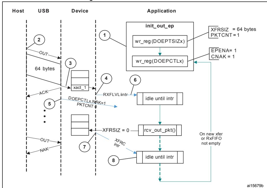
After a SetConfiguration/SetInterface command, the application initializes all OUT endpoints by setting CNAK = 1 and EPENA = 1 (in OTG_FS_DOEPCTLx), and setting a suitable XFRSIZ and PKTCNT in the OTG_FS_DOEPTSIZx register.
- 1. host attempts to send data (OUT token) to an endpoint.
- 2. When the core receives the OUT token on the USB, it stores the packet in the RxFIFO because space is available there.
- 3. After writing the complete packet in the RxFIFO, the core then asserts the RXFLVL interrupt (in OTG_FS_GINTSTS).
- 4. On receiving the PKTCNT number of USB packets, the core internally sets the NAK bit for this endpoint to prevent it from receiving any more packets.
- 5. The application processes the interrupt and reads the data from the RxFIFO.
- 6. When the application has read all the data (equivalent to XFRSIZ), the core generates an XFRC interrupt (in OTG_FS_DOEPINTx).
- 7. The application processes the interrupt and uses the setting of the XFRC interrupt bit (in OTG_FS_DOEPINTx) to determine that the intended transfer is complete.
IN data transfers
- • Packet write
This section describes how the application writes data packets to the endpoint FIFO when dedicated transmit FIFOs are enabled.
- 1. The application can either choose the polling or the interrupt mode.
- – In polling mode, the application monitors the status of the endpoint transmit data FIFO by reading the OTG_FS_DTXFSTSx register, to determine if there is enough space in the data FIFO.
- – In interrupt mode, the application waits for the TXFE interrupt (in OTG_FS_DIEPINTx) and then reads the OTG_FS_DTXFSTSx register, to determine if there is enough space in the data FIFO.
- – To write a single non-zero length data packet, there must be space to write the entire packet in the data FIFO.
- – To write zero length packet, the application must not look at the FIFO space.
- 2. Using one of the above mentioned methods, when the application determines that there is enough space to write a transmit packet, the application must first write into the endpoint control register, before writing the data into the data FIFO. Typically, the application, must do a read modify write on the OTG_FS_DIEPCTLx register to avoid modifying the contents of the register, except for setting the Endpoint Enable bit.
The application can write multiple packets for the same endpoint into the transmit FIFO, if space is available. For periodic IN endpoints, the application must write packets only for one microframe. It can write packets for the next periodic transaction only after getting transfer complete for the previous transaction.
- • Setting IN endpoint NAK
Internal data flow
- 1. When the application sets the IN NAK for a particular endpoint, the core stops transmitting data on the endpoint, irrespective of data availability in the endpoint's transmit FIFO.
- 2. Non-isochronous IN tokens receive a NAK handshake reply
- – Isochronous IN tokens receive a zero-data-length packet reply
- 3. The core asserts the INEPNE (IN endpoint NAK effective) interrupt in OTG_FS_DIEPINTx in response to the SNAK bit in OTG_FS_DIEPCTLx.
- 4. Once this interrupt is seen by the application, the application can assume that the endpoint is in IN NAK mode. This interrupt can be cleared by the application by setting the CNAK bit in OTG_FS_DIEPCTLx.
Application programming sequence
- 1. To stop transmitting any data on a particular IN endpoint, the application must set the IN NAK bit. To set this bit, the following field must be programmed.
- – SNAK = 1 in OTG_FS_DIEPCTLx
- 2. Wait for assertion of the INEPNE interrupt in OTG_FS_DIEPINTx. This interrupt indicates that the core has stopped transmitting data on the endpoint.
- 3. The core can transmit valid IN data on the endpoint after the application has set the NAK bit, but before the assertion of the NAK Effective interrupt.
- 4. The application can mask this interrupt temporarily by writing to the INEPNEM bit in DIEPMSK.
- – INEPNEM = 0 in DIEPMSK
- 5. To exit Endpoint NAK mode, the application must clear the NAK status bit (NAKSTS) in OTG_FS_DIEPCTLx. This also clears the INEPNE interrupt (in OTG_FS_DIEPINTx).
- – CNAK = 1 in OTG_FS_DIEPCTLx
- 6. If the application masked this interrupt earlier, it must be unmasked as follows:
- – INEPNEM = 1 in DIEPMSK
- • IN endpoint disable
Use the following sequence to disable a specific IN endpoint that has been previously enabled.
Application programming sequence
- 1. The application must stop writing data on the AHB for the IN endpoint to be disabled.
- 2. The application must set the endpoint in NAK mode.
- – SNAK = 1 in OTG_FS_DIEPCTLx
- 3. Wait for the INEPNE interrupt in OTG_FS_DIEPINTx.
- 4. Set the following bits in the OTG_FS_DIEPCTLx register for the endpoint that must be disabled.
- – EPDIS = 1 in OTG_FS_DIEPCTLx
- – SNAK = 1 in OTG_FS_DIEPCTLx
- 5. Assertion of the EPDISD interrupt in OTG_FS_DIEPINTx indicates that the core has completely disabled the specified endpoint. Along with the assertion of the interrupt, the core also clears the following bits:
- – EPENA = 0 in OTG_FS_DIEPCTLx
- – EPDIS = 0 in OTG_FS_DIEPCTLx
- 6. The application must read the OTG_FS_DIEPTSIx register for the periodic IN EP, to calculate how much data on the endpoint were transmitted on the USB.
- 7. The application must flush the data in the Endpoint transmit FIFO, by setting the following fields in the OTG_FS_GRSTCTL register:
- – TXFNUM (in OTG_FS_GRSTCTL) = Endpoint transmit FIFO number
- – TXFFLSH in (OTG_FS_GRSTCTL) = 1
The application must poll the OTG_FS_GRSTCTL register, until the TXFFLSH bit is cleared by the core, which indicates the end of flush operation. To transmit new data on this endpoint, the application can re-enable the endpoint at a later point.
- • Transfer Stop Programming for IN endpoints
The application must use the following programming sequence to stop any transfers (because of an interrupt from the host, typically a reset).
Sequence of operations:
- 1. Disable the IN endpoint by setting:
- – EPDIS = 1 in all OTG_FS_DIEPCTLx registers
- 2. Wait for the EPDIS interrupt in OTG_FS_DIEPINTx, which indicates that the IN endpoint is completely disabled. When the EPDIS interrupt is asserted the following bits are cleared:
- – EPDIS = 0 in OTG_FS_DIEPCTLx
- – EPENA = 0 in OTG_FS_DIEPCTLx
- 3. Flush the TxFIFO by programming the following bits:
- – TXFFLSH = 1 in OTG_FS_GRSTCTL
- – TXFNUM = ‘‘FIFO number specific to endpoint’’ in OTG_FS_GRSTCTL
- 4. The application can start polling till TXFFLSH in OTG_FS_GRSTCTL is cleared. When this bit is cleared, it ensures that there is no data left in the Tx FIFO.
- 1. Disable the IN endpoint by setting:
- • Generic non-periodic IN data transfers
Application requirements
- 1. Before setting up an IN transfer, the application must ensure that all data to be transmitted as part of the IN transfer are part of a single buffer.
- 2. For IN transfers, the Transfer Size field in the Endpoint Transfer Size register denotes a payload that constitutes multiple maximum-packet-size packets and a single short packet. This short packet is transmitted at the end of the transfer.
- – To transmit a few maximum-packet-size packets and a short packet at the end of the transfer:
Transfer size[EPNUM] = \( x \times \text{MPSIZ[EPNUM]} + \text{sp} \)
If ( \( \text{sp} > 0 \) ), then packet count[EPNUM] = \( x + 1 \) .
Otherwise, packet count[EPNUM] = \( x \)
- – To transmit a single zero-length data packet:
Transfer size[EPNUM] = 0
Packet count[EPNUM] = 1
- – To transmit a few maximum-packet-size packets and a zero-length data packet at the end of the transfer, the application must split the transfer into two parts. The first sends maximum-packet-size data packets and the second sends the zero-length data packet alone.
First transfer: transfer size[EPNUM] = \( x \times \text{MPSIZ[epnum]} \) ; packet count = \( n \) ;
Second transfer: transfer size[EPNUM] = 0; packet count = 1;
- – To transmit a few maximum-packet-size packets and a short packet at the end of the transfer:
- 3. Once an endpoint is enabled for data transfers, the core updates the Transfer size register. At the end of the IN transfer, the application must read the Transfer size register to determine how much data posted in the transmit FIFO have already been sent on the USB.
- 4. Data fetched into transmit FIFO = Application-programmed initial transfer size – core-updated final transfer size
- – Data transmitted on USB = (application-programmed initial packet count – Core updated final packet count) \( \times \text{MPSIZ[EPNUM]} \)
- – Data yet to be transmitted on USB = (Application-programmed initial transfer size – data transmitted on USB)
Internal data flow
- 1. The application must set the transfer size and packet count fields in the endpoint-specific registers and enable the endpoint to transmit the data.
- 2. The application must also write the required data to the transmit FIFO for the endpoint.
- 3. Every time a packet is written into the transmit FIFO by the application, the transfer size for that endpoint is decremented by the packet size. The data is fetched from the memory by the application, until the transfer size for the endpoint becomes 0. After writing the data into the FIFO, the “number of packets in FIFO” count is incremented (this is a 3-bit count, internally maintained by the core for each IN endpoint transmit FIFO. The maximum number of packets maintained by the core at any time in an IN endpoint FIFO is eight). For zero-length packets, a separate flag is set for each FIFO, without any data in the FIFO.
- 4. Once the data are written to the transmit FIFO, the core reads them out upon receiving an IN token. For every non-isochronous IN data packet transmitted with an ACK handshake, the packet count for the endpoint is decremented by one, until the packet count is zero. The packet count is not decremented on a timeout.
- 5. For zero length packets (indicated by an internal zero length flag), the core sends out a zero-length packet for the IN token and decrements the packet count field.
- 6. If there are no data in the FIFO for a received IN token and the packet count field for that endpoint is zero, the core generates an “IN token received when TxFIFO is empty” (ITTXFE) Interrupt for the endpoint, provided that the endpoint NAK bit is not set. The core responds with a NAK handshake for non-isochronous endpoints on the USB.
- 7. The core internally rewinds the FIFO pointers and no timeout interrupt is generated.
- 8. When the transfer size is 0 and the packet count is 0, the transfer complete (XFRC) interrupt for the endpoint is generated and the endpoint enable is cleared.
Application programming sequence
- 1. Program the OTG_FS_DIEPTSIx register with the transfer size and corresponding packet count.
- 2. Program the OTG_FS_DIEPCTLx register with the endpoint characteristics and set the CNAK and EPENA (Endpoint Enable) bits.
- 3. When transmitting non-zero length data packet, the application must poll the OTG_FS_DTXFSTSx register (where x is the FIFO number associated with that endpoint) to determine whether there is enough space in the data FIFO. The application can optionally use TXFE (in OTG_FS_DIEPINTx ) before writing the data.
- • Generic periodic IN data transfers
This section describes a typical periodic IN data transfer.
Application requirements
- 1. Application requirements 1, 2, 3, and 4 of
Generic non-periodic IN data transfers
also apply to periodic IN data transfers, except for a slight modification of requirement 2.
- – The application can only transmit multiples of maximum-packet-size data packets or multiples of maximum-packet-size packets, plus a short packet at the end. To transmit a few maximum-packet-size packets and a short packet at the end of the transfer, the following conditions must be met:\[ \text{transfer size[EPNUM]} = x \times \text{MPSIZ[EPNUM]} + \text{sp} \](where \( x \) is an integer \( \geq 0 \) , and \( 0 \leq \text{sp} < \text{MPSIZ[EPNUM]} \) )\[ \text{If (sp } > 0\text{), packet count[EPNUM]} = x + 1 \]Otherwise, packet count[EPNUM] = \( x \) ;
- – The application can only transmit multiples of maximum-packet-size data packets or multiples of maximum-packet-size packets, plus a short packet at the end. To transmit a few maximum-packet-size packets and a short packet at the end of the transfer, the following conditions must be met:
- MCNT[EPNUM] = packet count[EPNUM]
- – The application cannot transmit a zero-length data packet at the end of a transfer. It can transmit a single zero-length data packet by itself. To transmit a single zero-length data packet:
- – transfer size[EPNUM] = 0
- – packet count[EPNUM] = 1
- – MCNT[EPNUM] = packet count[EPNUM]
- 2. The application can only schedule data transfers one frame at a time.
- – \( (MCNT - 1) \times MPSIZ \leq XFERsiz \leq MCNT \times MPSIZ \)
- – PKTCNT = MCNT (in OTG_FS_DIEPTSIZx)
- – If \( XFERsiz < MCNT \times MPSIZ \) , the last data packet of the transfer is a short packet.
- – Note that: MCNT is in OTG_FS_DIEPTSIZx, MPSIZ is in OTG_FS_DIEPCTLx, PKTCNT is in OTG_FS_DIEPTSIZx and XFERsiz is in OTG_FS_DIEPTSIZx
- 3. The complete data to be transmitted in the frame must be written into the transmit FIFO by the application, before the IN token is received. Even when 1 word of the data to be transmitted per frame is missing in the transmit FIFO when the IN token is received, the core behaves as when the FIFO is empty. When the transmit FIFO is empty:
- – A zero data length packet would be transmitted on the USB for isochronous IN endpoints
- – A NAK handshake would be transmitted on the USB for interrupt IN endpoints
- 2. The application can only schedule data transfers one frame at a time.
Internal data flow
- 1. The application must set the transfer size and packet count fields in the endpoint-specific registers and enable the endpoint to transmit the data.
- 2. The application must also write the required data to the associated transmit FIFO for the endpoint.
- 3. Every time the application writes a packet to the transmit FIFO, the transfer size for that endpoint is decremented by the packet size. The data are fetched from application memory until the transfer size for the endpoint becomes 0.
- 4. When an IN token is received for a periodic endpoint, the core transmits the data in the FIFO, if available. If the complete data payload (complete packet, in dedicated FIFO mode) for the frame is not present in the FIFO, then the core generates an IN token received when TxFIFO empty interrupt for the endpoint.
- – A zero-length data packet is transmitted on the USB for isochronous IN endpoints
- – A NAK handshake is transmitted on the USB for interrupt IN endpoints
- 5. The packet count for the endpoint is decremented by 1 under the following conditions:
- – For isochronous endpoints, when a zero- or non-zero-length data packet is transmitted
- – For interrupt endpoints, when an ACK handshake is transmitted
- – When the transfer size and packet count are both 0, the transfer completed interrupt for the endpoint is generated and the endpoint enable is cleared.
- 6. At the “Periodic frame Interval” (controlled by PFIVL in OTG_FS_DCFG), when the core finds non-empty any of the isochronous IN endpoint FIFOs scheduled for the current frame non-empty, the core generates an IISOIXFR interrupt in OTG_FS_GINTSTS.
Application programming sequence
- 1. Program the OTG_FS_DIEPCTLx register with the endpoint characteristics and set the CNAK and EPENA bits.
- 2. Write the data to be transmitted in the next frame to the transmit FIFO.
- 3. Asserting the ITTXFE interrupt (in OTG_FS_DIEPINTx) indicates that the application has not yet written all data to be transmitted to the transmit FIFO.
- 4. If the interrupt endpoint is already enabled when this interrupt is detected, ignore the interrupt. If it is not enabled, enable the endpoint so that the data can be transmitted on the next IN token attempt.
- 5. Asserting the XFRC interrupt (in OTG_FS_DIEPINTx) with no ITTXFE interrupt in OTG_FS_DIEPINTx indicates the successful completion of an isochronous IN transfer. A read to the OTG_FS_DIEPTSIZx register must give transfer size = 0 and packet count = 0, indicating all data were transmitted on the USB.
- 6. Asserting the XFRC interrupt (in OTG_FS_DIEPINTx), with or without the ITTXFE interrupt (in OTG_FS_DIEPINTx), indicates the successful completion of an interrupt IN transfer. A read to the OTG_FS_DIEPTSIZx register must give transfer size = 0 and packet count = 0, indicating all data were transmitted on the USB.
- 7. Asserting the incomplete isochronous IN transfer (IISOIXFR) interrupt in OTG_FS_GINTSTS with none of the aforementioned interrupts indicates the core did not receive at least 1 periodic IN token in the current frame.
- • Incomplete isochronous IN data transfers
This section describes what the application must do on an incomplete isochronous IN data transfer.
Internal data flow
- 1. An isochronous IN transfer is treated as incomplete in one of the following conditions:
- a) The core receives a corrupted isochronous IN token on at least one isochronous IN endpoint. In this case, the application detects an incomplete isochronous IN transfer interrupt (IISOIXFR in OTG_FS_GINTSTS).
- b) The application is slow to write the complete data payload to the transmit FIFO and an IN token is received before the complete data payload is written to the FIFO. In this case, the application detects an IN token received when TxFIFO empty interrupt in OTG_FS_DIEPINTx. The application can ignore this interrupt, as it eventually results in an incomplete isochronous IN transfer interrupt (IISOIXFR in OTG_FS_GINTSTS) at the end of periodic frame.
The core transmits a zero-length data packet on the USB in response to the received IN token.
- 2. The application must stop writing the data payload to the transmit FIFO as soon as possible.
- 3. The application must set the NAK bit and the disable bit for the endpoint.
- 4. The core disables the endpoint, clears the disable bit, and asserts the Endpoint Disable interrupt for the endpoint.
Application programming sequence
- 1. The application can ignore the IN token received when TxFIFO empty interrupt in OTG_FS_DIEPINTx on any isochronous IN endpoint, as it eventually results in an incomplete isochronous IN transfer interrupt (in OTG_FS_GINTSTS).
- 2. Assertion of the incomplete isochronous IN transfer interrupt (in OTG_FS_GINTSTS) indicates an incomplete isochronous IN transfer on at least one of the isochronous IN endpoints.
- 3. The application must read the Endpoint Control register for all isochronous IN endpoints to detect endpoints with incomplete IN data transfers.
- 4. The application must stop writing data to the Periodic Transmit FIFOs associated with these endpoints on the AHB.
- 5. Program the following fields in the OTG_FS_DIEPCTLx register to disable the endpoint:
- – SNAK = 1 in OTG_FS_DIEPCTLx
- – EPDIS = 1 in OTG_FS_DIEPCTLx
- 6. The assertion of the Endpoint Disabled interrupt in OTG_FS_DIEPINTx indicates that the core has disabled the endpoint.
- – At this point, the application must flush the data in the associated transmit FIFO or overwrite the existing data in the FIFO by enabling the endpoint for a new transfer in the next microframe. To flush the data, the application must use the OTG_FS_GRSTCTL register.
- • Stalling non-isochronous IN endpoints
This section describes how the application can stall a non-isochronous endpoint.
Application programming sequence
- 1. Disable the IN endpoint to be stalled. Set the STALL bit as well.
- 2. EPDIS = 1 in OTG_FS_DIEPCTLx, when the endpoint is already enabled
- – STALL = 1 in OTG_FS_DIEPCTLx
- – The STALL bit always takes precedence over the NAK bit
- 3. Assertion of the Endpoint Disabled interrupt (in OTG_FS_DIEPINTx) indicates to the application that the core has disabled the specified endpoint.
- 4. The application must flush the non-periodic or periodic transmit FIFO, depending on the endpoint type. In case of a non-periodic endpoint, the application must re-enable the other non-periodic endpoints that do not need to be stalled, to transmit data.
- 5. Whenever the application is ready to end the STALL handshake for the endpoint, the STALL bit must be cleared in OTG_FS_DIEPCTLx.
- 6. If the application sets or clears a STALL bit for an endpoint due to a SetFeature.Endpoint Halt command or ClearFeature.Endpoint Halt command, the STALL bit must be set or cleared before the application sets up the Status stage transfer on the control endpoint.
Special case: stalling the control OUT endpoint
The core must stall IN/OUT tokens if, during the data stage of a control transfer, the host sends more IN/OUT tokens than are specified in the SETUP packet. In this case, the application must enable the ITTXFE interrupt in OTG_FS_DIEPINTx and the OTEPDIS interrupt in OTG_FS_DOEPINTx during the data stage of the control transfer, after the core has transferred the amount of data specified in the SETUP packet. Then, when the application receives this interrupt, it must set the STALL bit in the corresponding endpoint control register, and clear this interrupt.
22.17.7 Worst case response time
When the OTG_FS controller acts as a device, there is a worst case response time for any tokens that follow an isochronous OUT. This worst case response time depends on the AHB clock frequency.
The core registers are in the AHB domain, and the core does not accept another token before updating these register values. The worst case is for any token following an isochronous OUT, because for an isochronous transaction, there is no handshake and the next token could come sooner. This worst case value is 7 PHY clocks when the AHB clock is the same as the PHY clock. When the AHB clock is faster, this value is smaller.
If this worst case condition occurs, the core responds to bulk/interrupt tokens with a NAK and drops isochronous and SETUP tokens. The host interprets this as a timeout condition for SETUP and retries the SETUP packet. For isochronous transfers, the Incomplete isochronous IN transfer interrupt (IISOIXFR) and Incomplete isochronous OUT transfer interrupt (IISOOXFR) inform the application that isochronous IN/OUT packets were dropped.
Choosing the value of TRDT in OTG_FS_GUSBCFG
The value in TRDT (OTG_FS_GUSBCFG) is the time it takes for the MAC, in terms of PHY clocks after it has received an IN token, to get the FIFO status, and thus the first data from the PFC block. This time involves the synchronization delay between the PHY and AHB clocks. The worst case delay for this is when the AHB clock is the same as the PHY clock. In this case, the delay is 5 clocks.
Once the MAC receives an IN token, this information (token received) is synchronized to the AHB clock by the PFC (the PFC runs on the AHB clock). The PFC then reads the data from the SPRAM and writes them into the dual clock source buffer. The MAC then reads the data out of the source buffer (4 deep).
If the AHB is running at a higher frequency than the PHY, the application can use a smaller value for TRDT (in OTG_FS_GUSBCFG).
Figure 261 has the following signals:
- • tkn_rcvd: Token received information from MAC to PFC
- • dynccd_tkn_rcvd: Doubled sync tkn_rcvd, from PCLK to HCLK domain
- • spr_read: Read to SPRAM
- • spr_addr: Address to SPRAM
- • spr_rdata: Read data from SPRAM
- • srcbuf_push: Push to the source buffer
- • srcbuf_rdata: Read data from the source buffer. Data seen by MAC
Refer to Table 133: TRDT values for the values of TRDT versus AHB clock frequency.
Figure 261. TRDT max timing case
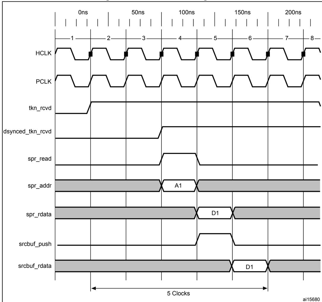
The timing diagram illustrates the TRDT max timing case for the OTG_FS controller. It shows the relationship between several signals over a 200ns period, divided into 8 clock cycles. The signals are:
- HCLK : High-frequency clock signal.
- PCLK : Peripheral clock signal.
- tkn_rcvd : Token received signal, which goes high at the start of the sequence.
- dsynced_tkn_rcvd : De-synchronized token received signal, which goes high at the start of the sequence.
- spr_read : Sprout read signal, which goes high at the start of the sequence.
- spr_addr : Sprout address signal, which is high during the first 5 clock cycles and then goes low. It contains a label 'A1'.
- spr_rdata : Sprout read data signal, which is high during the first 5 clock cycles and then goes low. It contains a label 'D1'.
- srcbuf_push : Source buffer push signal, which goes high at the start of the sequence.
- srcbuf_rdata : Source buffer read data signal, which is high during the first 5 clock cycles and then goes low. It contains a label 'D1'.
A double-headed arrow at the bottom indicates a duration of 5 Clocks, spanning from the start of the sequence to the end of the 5th clock cycle.
ai15680
22.17.8 OTG programming model
The OTG_FS controller is an OTG device supporting HNP and SRP. When the core is connected to an “A” plug, it is referred to as an A-device. When the core is connected to a “B” plug it is referred to as a B-device. In host mode, the OTG_FS controller turns off \( V_{BUS} \) to conserve power. SRP is a method by which the B-device signals the A-device to turn on \( V_{BUS} \) power. A device must perform both data-line pulsing and \( V_{BUS} \) pulsing, but a host can detect either data-line pulsing or \( V_{BUS} \) pulsing for SRP. HNP is a method by which the B-device negotiates and switches to host role. In Negotiated mode after HNP, the B-device suspends the bus and reverts to the device role.
A-device session request protocol
The application must set the SRP-capable bit in the Core USB configuration register. This enables the OTG_FS controller to detect SRP as an A-device.
Figure 262. A-device SRP
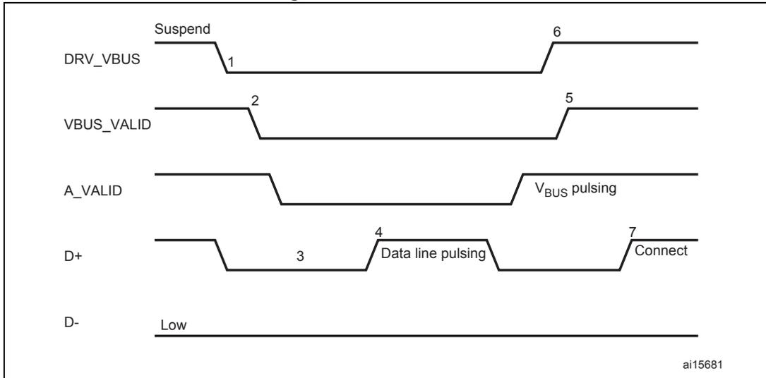
- 1. DRV_VBUS = \( V_{BUS} \) drive signal to the PHY
- VBUS_VALID = \( V_{BUS} \) valid signal from PHY
- A_VALID = A-peripheral \( V_{BUS} \) level signal to PHY
- D+ = Data plus line
- D- = Data minus line
- 1. To save power, the application suspends and turns off port power when the bus is idle by writing the port suspend and port power bits in the host port control and status register.
- 2. PHY indicates port power off by deasserting the VBUS_VALID signal.
- 3. The device must detect SE0 for at least 2 ms to start SRP when \( V_{BUS} \) power is off.
- 4. To initiate SRP, the device turns on its data line pull-up resistor for 5 to 10 ms. The OTG_FS controller detects data-line pulsing.
- 5. The device drives
\(
V_{BUS}
\)
above the A-device session valid (2.0 V minimum) for
\(
V_{BUS}
\)
pulsing.
The OTG_FS controller interrupts the application on detecting SRP. The Session request detected bit is set in Global interrupt status register (SRQINT set in OTG_FS_GINTSTS). - 6. The application must service the Session request detected interrupt and turn on the port power bit by writing the port power bit in the host port control and status register. The PHY indicates port power-on by asserting the VBUS_VALID signal.
- 7. When the USB is powered, the device connects, completing the SRP process.
B-device session request protocol
The application must set the SRP-capable bit in the Core USB configuration register. This enables the OTG_FS controller to initiate SRP as a B-device. SRP is a means by which the OTG_FS controller can request a new session from the host.
Figure 263. B-device SRP
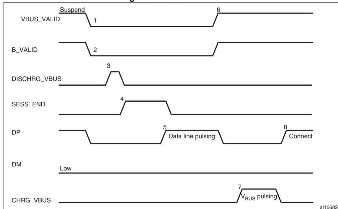
- 1. VBUS_VALID = V BUS valid signal from PHY
- B_VALID = B-peripheral valid session to PHY
- DISCHRG_VBUS = discharge signal to PHY
- SESS_END = session end signal to PHY
- CHRG_VBUS = charge V BUS signal to PHY
- DP = Data plus line
- DM = Data minus line
To save power, the host suspends and turns off port power when the bus is idle.
The OTG_FS controller sets the early suspend bit in the Core interrupt register after 3 ms of bus idleness. Following this, the OTG_FS controller sets the USB suspend bit in the Core interrupt register.
The OTG_FS controller informs the PHY to discharge V BUS .
The PHY indicates the session's end to the device. This is the initial condition for SRP.
The OTG_FS controller requires 2 ms of SE0 before initiating SRP.
For a USB 1.1 full-speed serial transceiver, the application must wait until V BUS discharges to 0.2 V after BSVLD (in OTG_FS_GOTGCTL) is deasserted. This discharge time can be obtained from the transceiver vendor and varies from one transceiver to another.
- The USB OTG core informs the PHY to speed up V BUS discharge.
- The application initiates SRP by writing the session request bit in the OTG Control and status register. The OTG_FS controller perform data-line pulsing followed by V BUS pulsing.
The host detects SRP from either the data-line or V BUS pulsing, and turns on V BUS .
The PHY indicates V BUS power-on to the device.
- 6. The OTG_FS controller performs
\(
V_{BUS}
\)
pulsing.
The host starts a new session by turning on \( V_{BUS} \) , indicating SRP success. The OTG_FS controller interrupts the application by setting the session request success status change bit in the OTG interrupt status register. The application reads the session request success bit in the OTG control and status register. - 7. When the USB is powered, the OTG_FS controller connects, completing the SRP process.
A-device host negotiation protocol
HNP switches the USB host role from the A-device to the B-device. The application must set the HNP-capable bit in the Core USB configuration register to enable the OTG_FS controller to perform HNP as an A-device.
Figure 264. A-device HNP
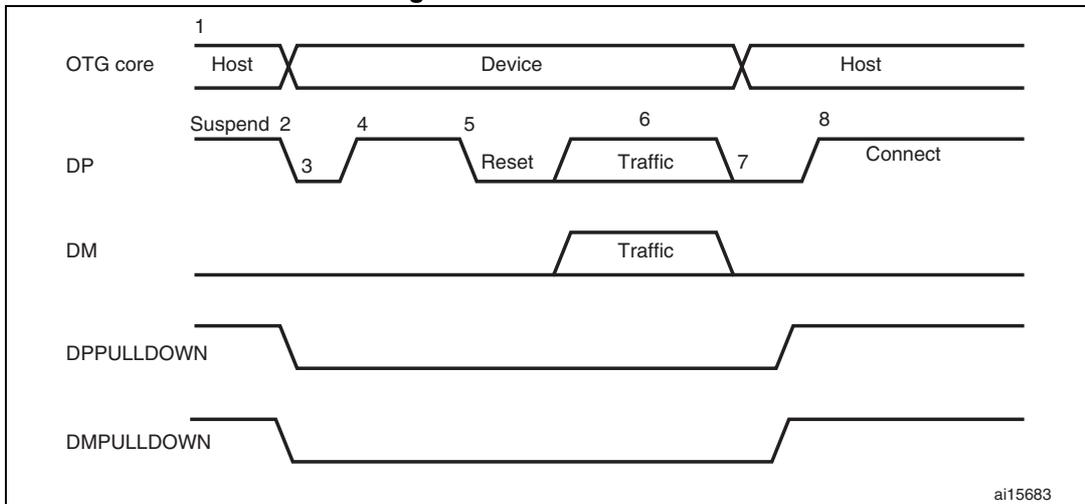
The timing diagram illustrates the A-device HNP process across eight numbered stages. 1. OTG core : Starts as 'Host', transitions to 'Device' between stages 2 and 7, and returns to 'Host' at stage 8. 2. DP (Data Plus) : Shows 'Suspend' at stage 2, drops low at stage 3, rises at stage 4, undergoes 'Reset' at stage 5, shows 'Traffic' at stage 6, and 'Connect' at stage 8. 3. DM (Data Minus) : Shows 'Traffic' during stage 6. 4. DPPULLDOWN & DMPULLDOWN : Both signals are high during the initial 'Host' phase, drop low during the 'Device' phase (stages 2-7), and return high when the core reverts to 'Host' at stage 8.
- 1. DPPULLDOWN = signal from core to PHY to enable/disable the pull-down on the DP line inside the PHY.
DMPULLDOWN = signal from core to PHY to enable/disable the pull-down on the DM line inside the PHY. - 1. The OTG_FS controller sends the B-device a SetFeature b_hnp_enable descriptor to enable HNP support. The B-device’s ACK response indicates that the B-device supports HNP. The application must set host Set HNP Enable bit in the OTG Control
and status register to indicate to the OTG_FS controller that the B-device supports HNP.
- 2. When it has finished using the bus, the application suspends by writing the Port suspend bit in the host port control and status register.
- 3. When the B-device observes a USB suspend, it disconnects, indicating the initial condition for HNP. The B-device initiates HNP only when it must switch to the host role; otherwise, the bus continues to be suspended.
The OTG_FS controller sets the host negotiation detected interrupt in the OTG interrupt status register, indicating the start of HNP.
The OTG_FS controller deasserts the DM pull down and DM pull down in the PHY to indicate a device role. The PHY enables the OTG_FS_DP pull-up resistor to indicate a connect for B-device.
The application must read the current mode bit in the OTG Control and status register to determine device mode operation.
- 4. The B-device detects the connection, issues a USB reset, and enumerates the OTG_FS controller for data traffic.
- 5. The B-device continues the host role, initiating traffic, and suspends the bus when done.
The OTG_FS controller sets the early suspend bit in the Core interrupt register after 3 ms of bus idleness. Following this, the OTG_FS controller sets the USB Suspend bit in the Core interrupt register.
- 6. In Negotiated mode, the OTG_FS controller detects the suspend, disconnects, and switches back to the host role. The OTG_FS controller asserts the DM pull down and DM pull down in the PHY to indicate its assumption of the host role.
- 7. The OTG_FS controller sets the Connector ID status change interrupt in the OTG Interrupt Status register. The application must read the connector ID status in the OTG Control and Status register to determine the OTG_FS controller operation as an A-device. This indicates the completion of HNP to the application. The application must read the Current mode bit in the OTG control and status register to determine host mode operation.
- 8. The B-device connects, completing the HNP process.
B-device host negotiation protocol
HNP switches the USB host role from B-device to A-device. The application must set the HNP-capable bit in the Core USB configuration register to enable the OTG_FS controller to perform HNP as a B-device.
Figure 265. B-device HNP
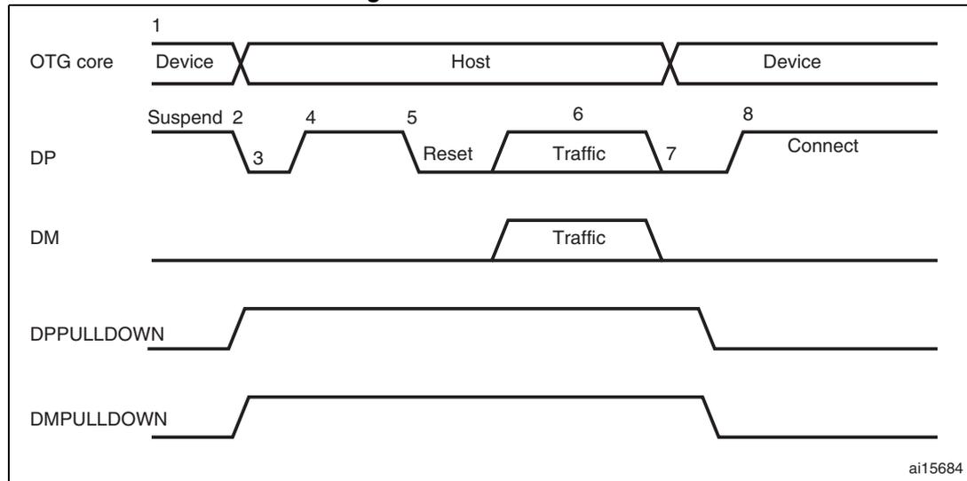
The diagram illustrates the timing sequence for B-device Host Negotiation Protocol (HNP). It consists of five horizontal signal lines over time, with events numbered 1 through 8.
- OTG core: Shows the role of the OTG core. It starts as a Device (1), switches to Host (2-7), and returns to Device (8).
- DP: The Data Plus line. It starts in a Suspend state (1), goes to a low-voltage state (3), then a Reset state (5), followed by Traffic (6), and finally a Connect state (8).
- DM: The Data Minus line. It is idle during suspend and reset, then carries Traffic (6) when the core is in Host mode.
- DPPULLDOWN: A signal from the OTG core to the PHY. It is active (low) during the Host mode (2-7) to pull down the DP line.
- DMPULLDOWN: A signal from the OTG core to the PHY. It is active (low) during the Host mode (2-7) to pull down the DM line.
ai15684
- 1. DPPULLDOWN = signal from core to PHY to enable/disable the pull-down on the DP line inside the PHY.
DMPULLDOWN = signal from core to PHY to enable/disable the pull-down on the DM line inside the PHY.
- 1. The A-device sends the SetFeature b_hnp_enable descriptor to enable HNP support. The OTG_FS controller's ACK response indicates that it supports HNP. The application must set the device HNP enable bit in the OTG Control and status register to indicate HNP support.
The application sets the HNP request bit in the OTG Control and status register to indicate to the OTG_FS controller to initiate HNP.
- 2. When it has finished using the bus, the A-device suspends by writing the Port suspend bit in the host port control and status register.
The OTG_FS controller sets the Early suspend bit in the Core interrupt register after 3 ms of bus idleness. Following this, the OTG_FS controller sets the USB suspend bit in the Core interrupt register.
The OTG_FS controller disconnects and the A-device detects SE0 on the bus, indicating HNP. The OTG_FS controller asserts the DP pull down and DM pull down in the PHY to indicate its assumption of the host role.
The A-device responds by activating its OTG_FS_DP pull-up resistor within 3 ms of detecting SE0. The OTG_FS controller detects this as a connect.
The OTG_FS controller sets the host negotiation success status change interrupt in the OTG Interrupt status register, indicating the HNP status. The application must read the host negotiation success bit in the OTG Control and status register to determine host negotiation success. The application must read the current Mode bit in the Core interrupt register (OTG_FS_GINTSTS) to determine host mode operation.
- 3. The application sets the reset bit (PRST in OTG_FS_HPRT) and the OTG_FS controller issues a USB reset and enumerates the A-device for data traffic.
- 4. The OTG_FS controller continues the host role of initiating traffic, and when done, suspends the bus by writing the Port suspend bit in the host port control and status register.
- 5. In Negotiated mode, when the A-device detects a suspend, it disconnects and switches back to the host role. The OTG_FS controller deasserts the DP pull down and DM pull down in the PHY to indicate the assumption of the device role.
- 6. The application must read the current mode bit in the Core interrupt (OTG_FS_GINTSTS) register to determine the host mode operation.
- 7. The OTG_FS controller connects, completing the HNP process.