21. Secure digital input/output interface (SDIO)
21.1 SDIO main features
The SD/SDIO MMC card host interface (SDIO) provides an interface between the APB2 peripheral bus and MultiMediaCards (MMCs), SD memory cards, SDIO cards and CE-ATA devices.
The MultiMediaCard system specifications are available through the MultiMediaCard Association website at http://www.jedec.org/ , published by the MMCA technical committee.
SD memory card and SD I/O card system specifications are available through the SD card Association website at http://www.sdcard.org .
CE-ATA system specifications are available through the CE-ATA workgroup website.
The SDIO features include the following:
- • Full compliance with MultiMediaCard System Specification Version 4.2 . Card support for three different databus modes: 1-bit (default), 4-bit and 8-bit
- • Full compatibility with previous versions of MultiMediaCards (forward compatibility)
- • Full compliance with SD Memory Card Specifications Version 2.0
- • Full compliance with SD I/O Card Specification Version 2.0 : card support for two different databus modes: 1-bit (default) and 4-bit
- • Full support of the CE-ATA features (full compliance with CE-ATA digital protocol Rev1.1 )
- • Data transfer up to 50 MHz for the 8 bit mode
- • Data and command output enable signals to control external bidirectional drivers.
Note: The SDIO does not have an SPI-compatible communication mode.
The SD memory card protocol is a superset of the MultiMediaCard protocol as defined in the MultiMediaCard system specification V2.11. Several commands required for SD memory devices are not supported by either SD I/O-only cards or the I/O portion of combo cards. Some of these commands have no use in SD I/O devices, such as erase commands, and thus are not supported in the SDIO. In addition, several commands are different between SD memory cards and SD I/O cards and thus are not supported in the SDIO. For details refer to SD I/O card Specification Version 1.0. CE-ATA is supported over the MMC electrical interface using a protocol that utilizes the existing MMC access primitives. The interface electrical and signaling definition is as defined in the MMC reference.
The MultiMediaCard/SD bus connects cards to the controller.
The current version of the SDIO supports only one SD/SDIO/MMC4.2 card at any one time and a stack of MMC4.1 or previous.
21.2 SDIO bus topology
Communication over the bus is based on command and data transfers.
The basic transaction on the MultiMediaCard/SD/SD I/O bus is the command/response transaction. These types of bus transaction transfer their information directly within the command or response structure. In addition, some operations have a data token.
Data transfers to/from SD/SDIO memory cards are done in data blocks. Data transfers to/from MMC are done data blocks or streams. Data transfers to/from the CE-ATA Devices are done in data blocks.
Figure 229. SDIO “no response” and “no data” operations
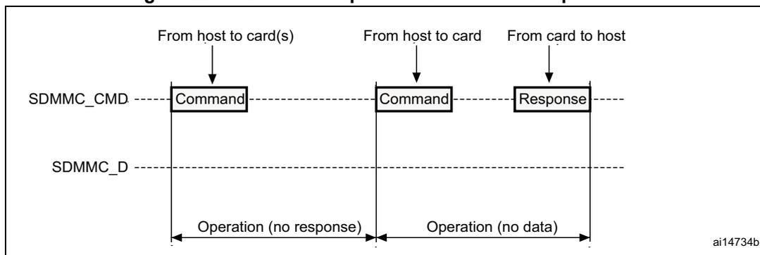
Figure 229 illustrates two SDIO operations. The first operation shows a 'Command' being sent from the host to card(s) via the SDMMC_CMD line, but no 'Response' is received, labeled as 'Operation (no response)'. The second operation shows a 'Command' being sent from the host to card via the SDMMC_CMD line, but no 'Data' is received, labeled as 'Operation (no data)'. The diagram includes labels for 'From host to card(s)', 'From host to card', and 'From card to host'.
Figure 230. SDIO (multiple) block read operation
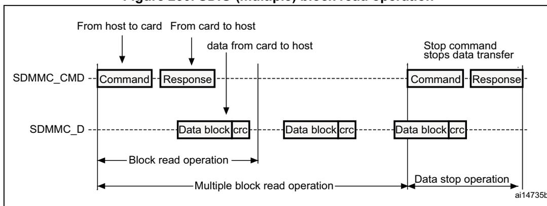
Figure 230 illustrates a multiple block read operation. It starts with a 'Command' being sent from the host to the card via the SDMMC_CMD line, and a 'Response' being received from the card. This is followed by a series of 'Data block' transfers from the card to the host via the SDMMC_D line, each followed by a 'crc'. The operation is labeled as 'Multiple block read operation'. The operation ends with a 'Stop command' being sent from the host to the card, which receives a 'Response', labeled as 'Data stop operation'.
Figure 231. SDIO (multiple) block write operation
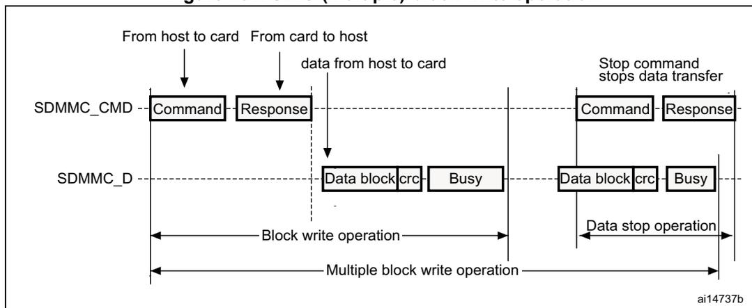
Figure 231 illustrates a multiple block write operation. It starts with a 'Command' being sent from the host to the card via the SDMMC_CMD line, and a 'Response' being received from the card. This is followed by a series of 'Data block' transfers from the host to the card via the SDMMC_D line, each followed by a 'crc' and a 'Busy' signal. The operation is labeled as 'Multiple block write operation'. The operation ends with a 'Stop command' being sent from the host to the card, which receives a 'Response', labeled as 'Data stop operation'.
Note: The SDIO does not send any data as long as the Busy signal is asserted (SDIO_D0 pulled low).
Figure 232. SDIO sequential read operation
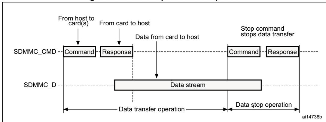
This sequence diagram illustrates the SDIO sequential read operation. It shows two horizontal timelines: SDMMC_CMD and SDMMC_D. 1. **Command**: A 'From host to card(s)' arrow points to the SDMMC_CMD line, followed by a 'Command' block. 2. **Response**: A 'From card to host' arrow points to the SDMMC_CMD line, followed by a 'Response' block. 3. **Data Transfer**: A 'Data from card to host' arrow points to the SDMMC_D line, which contains a 'Data stream' block. This period is labeled 'Data transfer operation'. 4. **Stop Command**: A 'From host to card(s)' arrow points to the SDMMC_CMD line, followed by a 'Command' block. A note indicates 'Stop command stops data transfer'. 5. **Final Response**: A 'From card to host' arrow points to the SDMMC_CMD line, followed by a 'Response' block. 6. **Data Stop**: The SDMMC_D line ends with a 'Data stop operation' label. The diagram is labeled ai14738b.
Figure 233. SDIO sequential write operation
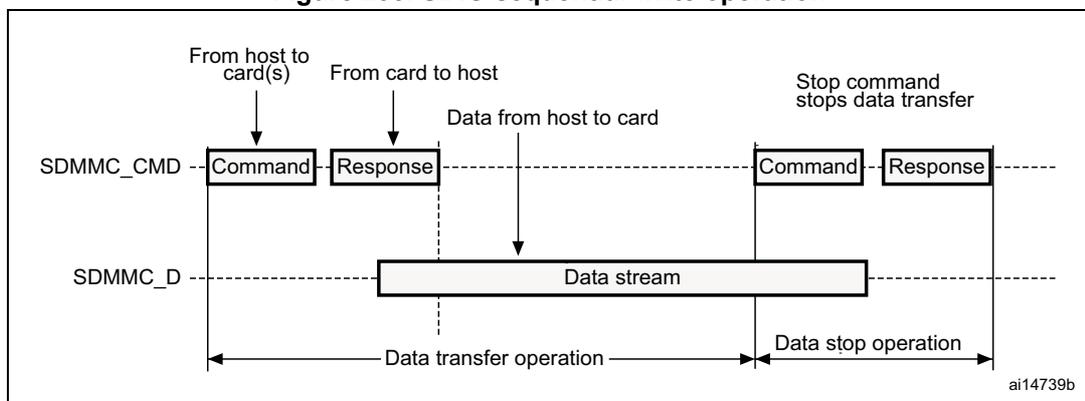
This sequence diagram illustrates the SDIO sequential write operation. It shows two horizontal timelines: SDMMC_CMD and SDMMC_D. 1. **Command**: A 'From host to card(s)' arrow points to the SDMMC_CMD line, followed by a 'Command' block. 2. **Response**: A 'From card to host' arrow points to the SDMMC_CMD line, followed by a 'Response' block. 3. **Data Transfer**: A 'Data from host to card' arrow points to the SDMMC_D line, which contains a 'Data stream' block. This period is labeled 'Data transfer operation'. 4. **Stop Command**: A 'From host to card(s)' arrow points to the SDMMC_CMD line, followed by a 'Command' block. A note indicates 'Stop command stops data transfer'. 5. **Final Response**: A 'From card to host' arrow points to the SDMMC_CMD line, followed by a 'Response' block. 6. **Data Stop**: The SDMMC_D line ends with a 'Data stop operation' label. The diagram is labeled ai14739b.
21.3 SDIO functional description
The SDIO consists of two parts:
- • The SDIO adapter block provides all functions specific to the MMC/SD/SD I/O card such as the clock generation unit, command and data transfer.
- • The APB2 interface accesses the SDIO adapter registers, and generates interrupt and DMA request signals.
Figure 234. SDIO block diagram
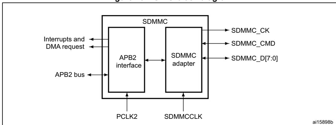
This block diagram shows the internal structure of the SDMMC block. - The main block is labeled 'SDMMC'. - Inside, there are two sub-blocks: 'APB2 interface' and 'SDMMC adapter'. - The 'APB2 interface' is connected to an external 'APB2 bus' and generates 'Interrupts and DMA request' signals. - The 'APB2 interface' and 'SDMMC adapter' are connected to each other by a bidirectional bus. - The 'SDMMC adapter' has three external output signals: 'SDMMC_CK' (clock), 'SDMMC_CMD' (command), and 'SDMMC_D[7:0]' (data bus). - The 'SDMMC adapter' also receives two external input signals: 'PCLK2' (bus clock) and 'SDMMCCLK' (card clock). The diagram is labeled ai15898b.
By default SDIO_D0 is used for data transfer. After initialization, the host can change the databus width.
If a MultiMediaCard is connected to the bus, SDIO_D0, SDIO_D[3:0] or SDIO_D[7:0] can be used for data transfer. MMC V3.31 or previous, supports only 1 bit of data so only SDIO_D0 can be used.
If an SD or SD I/O card is connected to the bus, data transfer can be configured by the host to use SDIO_D0 or SDIO_D[3:0]. All data lines are operating in push-pull mode.
SDIO_CMD has two operational modes:
- • Open-drain for initialization (only for MMCV3.31 or previous)
- • Push-pull for command transfer (SD/SD I/O card MMC4.2 use push-pull drivers also for initialization)
SDIO_CK is the clock to the card: one bit is transferred on both command and data lines with each clock cycle.
The SDIO uses two clock signals:
- • SDIO adapter clock SDIOCLK up to 50 MHz (48 MHz when in use with USB)
- • APB2 bus clock (PCLK2)
PCLK2 and SDIO_CK clock frequencies must respect the following condition:
The signals shown in Table 94 are used on the MultiMediaCard/SD/SD I/O card bus.
Table 94. SDIO I/O definitions
| Pin | Direction | Description |
|---|---|---|
| SDIO_CK | Output | MultiMediaCard/SD/SDIO card clock. This pin is the clock from host to card. |
| SDIO_CMD | Bidirectional | MultiMediaCard/SD/SDIO card command. This pin is the bidirectional command/response signal. |
| SDIO_D[7:0] | Bidirectional | MultiMediaCard/SD/SDIO card data. These pins are the bidirectional databus. |
21.3.1 SDIO adapter
Figure 235 shows a simplified block diagram of an SDIO adapter.
![Figure 235. SDIO adapter block diagram. The diagram shows the internal structure of the SDMMC adapter. On the left, an 'Adapter registers' block and a 'FIFO' block are connected to an 'APB2 interface'. These are clocked by 'PCLK2'. In the center, a 'Control unit', 'Command path', and 'Data path' are shown. The 'Control unit' is connected to the 'Adapter registers' and 'FIFO', and to the 'Command path' and 'Data path'. The 'Command path' is connected to 'SDMMC_CMD'. The 'Data path' is connected to 'SDMMC_D[7:0]'. Both 'Command path' and 'Data path' are clocked by 'SDMMCCLK'. On the right, a vertical double-headed arrow labeled 'Card bus' indicates the connection to the card. The diagram is labeled 'ai15899b' in the bottom right corner.](/RM0368-STM32F401xB-C-401xD-E/f28a7aa9754fc00b41d64c3e2f0106a0_img.jpg)
Figure 235. SDIO adapter
The SDIO adapter is a multimedia/secure digital memory card bus master that provides an interface to a multimedia card stack or to a secure digital memory card. It consists of five subunits:
- • Adapter register block
- • Control unit
- • Command path
- • Data path
- • Data FIFO
Note: The adapter registers and FIFO use the APB2 bus clock domain (PCLK2). The control unit, command path and data path use the SDIO adapter clock domain (SDIOCLK).
Adapter register block
The adapter register block contains all system registers. This block also generates the signals that clear the static flags in the multimedia card. The clear signals are generated when 1 is written into the corresponding bit location in the SDIO Clear register.
Control unit
The control unit contains the power management functions and the clock divider for the memory card clock.
There are three power phases:
- • power-off
- • power-up
- • power-on
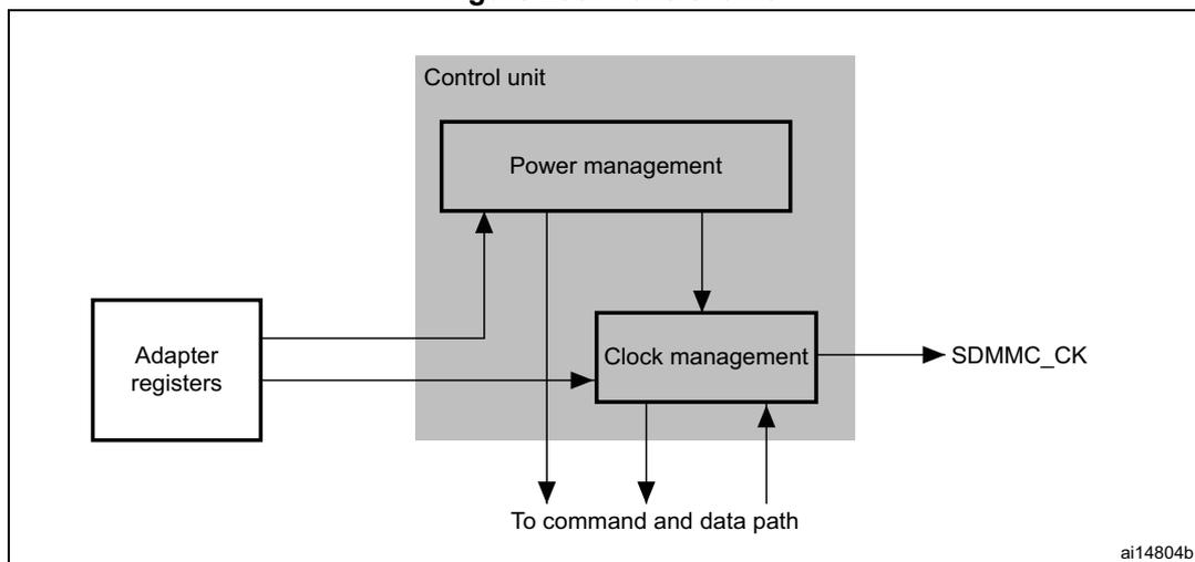
Figure 236. Control unit
graph TD
    subgraph Control_unit [Control unit]
        PM[Power management]
        CM[Clock management]
        PM --> CM
    end
    AR[Adapter registers] --> PM
    CM --> SDMMC_CK[SDMMC_CK]
CM --> CDP[To command and data path]The control unit is illustrated in Figure 236 . It consists of a power management subunit and a clock management subunit.
The power management subunit disables the card bus output signals during the power-off and power-up phases.
The clock management subunit generates and controls the SDIO_CK signal. The SDIO_CK output can use either the clock divide or the clock bypass mode. The clock output is inactive:
- • after reset
- • during the power-off or power-up phases
- • if the power saving mode is enabled and the card bus is in the Idle state (eight clock periods after both the command and data path subunits enter the Idle phase)
Command path
The command path unit sends commands to and receives responses from the cards.
Figure 237. SDIO adapter command path
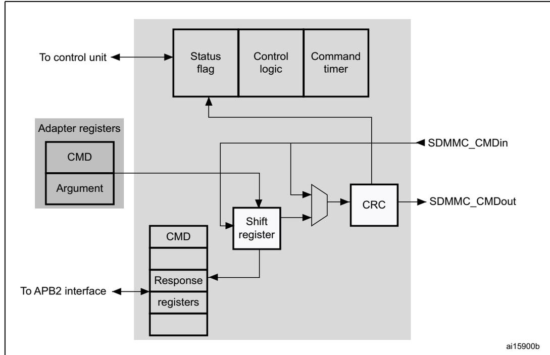
The diagram illustrates the internal architecture of the SDIO adapter command path. It features several key components and their interconnections:
- Control Unit Interface: A block labeled "To control unit" is connected to a "Status flag" register.
- Control Logic Block: A large block contains "Status flag", "Control logic", and "Command timer".
- Adapter Registers: A block labeled "Adapter registers" contains "CMD" and "Argument" registers. The "CMD" register is connected to a "Shift register".
- APB2 Interface: A block labeled "To APB2 interface" is connected to a "Response registers" block.
- Response Registers: A block labeled "Response registers" contains "CMD" and "Response" registers. It is connected to the "Shift register" and the "APB2 interface".
- Shift Register: A "Shift register" block receives data from the "CMD" register and sends data to the "CRC" block and the "Response registers".
- CRC Block: A "CRC" block receives data from the "Shift register" and outputs to "SDMMC_CMDout".
- External Connections:
- "SDMMC_CMDin" is an input signal to the "Control logic".
- "SDMMC_CMDout" is an output signal from the "CRC" block.
The diagram is labeled with "ai15900b" in the bottom right corner.
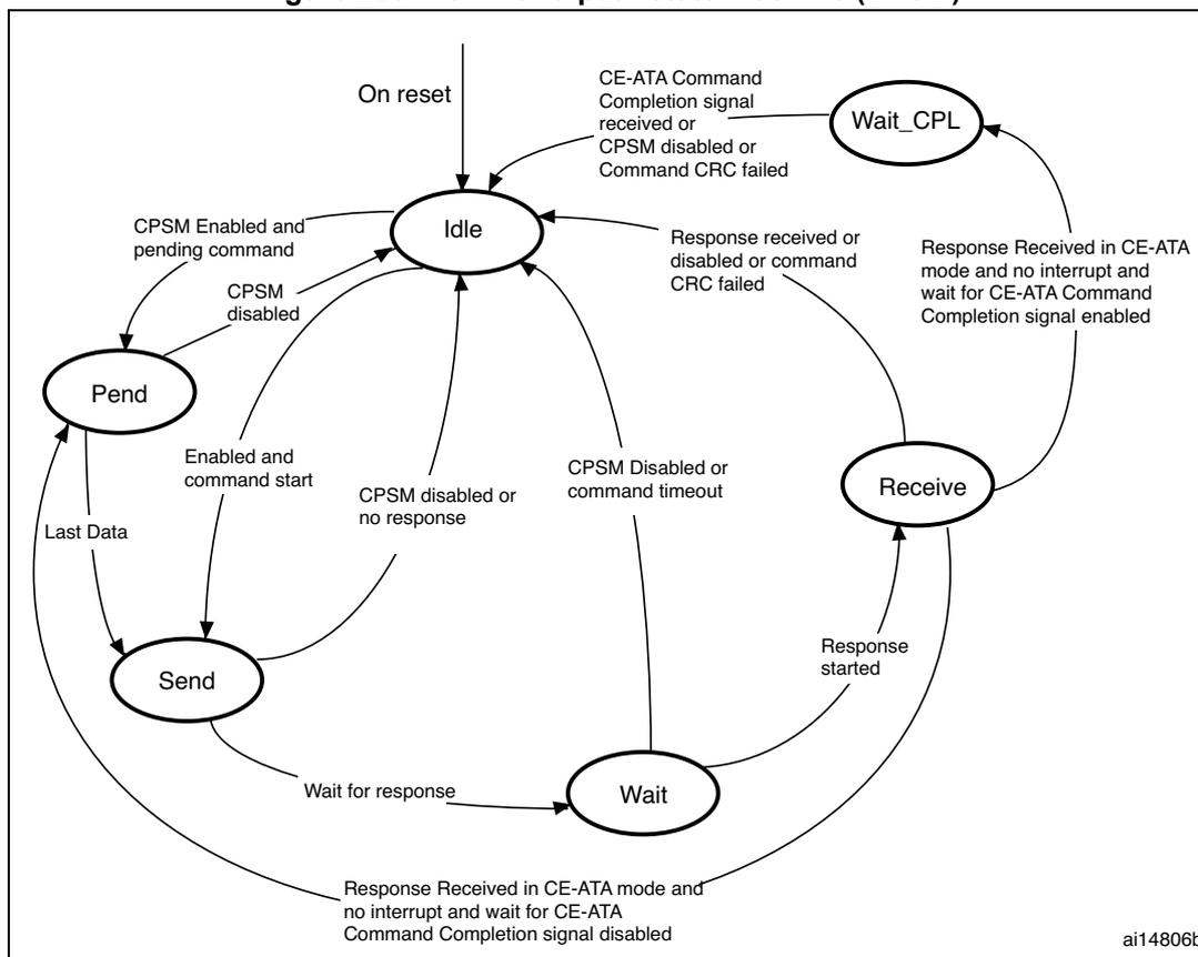
- • Command path state machine (CPSM)
- – When the command register is written to and the enable bit is set, command transfer starts. When the command has been sent, the command path state machine (CPSM) sets the status flags and enters the Idle state if a response is not required. If a response is required, it waits for the response (see Figure 238 on page 619 ). When the response is received, the received CRC code and the internally generated code are compared, and the appropriate status flags are set.
Figure 238. Command path state machine (CPSM)
stateDiagram-v2
    [*] --> Idle : On reset
    Idle --> Pend : CPSM Enabled and pending command
    Pend --> Idle : CPSM disabled
    Pend --> Send : Enabled and command start
    Send --> Idle : CPSM disabled or no response
    Send --> Wait : Wait for response
    Send --> Pend : Last Data
    Wait --> Idle : CPSM Disabled or command timeout
    Wait --> Receive : Response started
    Wait --> Send : Response Received in CE-ATA mode and no interrupt and wait for CE-ATA Command Completion signal disabled
    Receive --> Idle : Response received or disabled or command CRC failed
    Receive --> Wait_CPL : Response Received in CE-ATA mode and no interrupt and wait for CE-ATA Command Completion signal enabled
    Wait_CPL --> Idle : CE-ATA Command Completion signal received or CPSM disabled or Command CRC failed
When the Wait state is entered, the command timer starts running. If the timeout is reached before the CPSM moves to the Receive state, the timeout flag is set and the Idle state is entered.
Note: The command timeout has a fixed value of 64 SDIO_CK clock periods.
If the interrupt bit is set in the command register, the timer is disabled and the CPSM waits for an interrupt request from one of the cards. If a pending bit is set in the command register, the CPSM enters the Pend state, and waits for a CmdPend signal from the data path subunit. When CmdPend is detected, the CPSM moves to the Send state. This enables the data counter to trigger the stop command transmission.
Note: The CPSM remains in the Idle state for at least eight SDIO_CK periods to meet the \( N_{CC} \) and \( N_{RC} \) timing constraints. \( N_{CC} \) is the minimum delay between two host commands, and \( N_{RC} \) is the minimum delay between the host command and the card response.
Figure 239. SDIO command transfer
- • Command format
- – Command: a command is a token that starts an operation. Command are sent from the host either to a single card (addressed command) or to all connected cards (broadcast command are available for MMC V3.31 or previous). Commands are transferred serially on the CMD line. All commands have a fixed length of 48 bits. The general format for a command token for MultiMediaCards, SD-Memory cards and SDIO-Cards is shown in Table 95 . CE-ATA commands are an extension of MMC commands V4.2, and so have the same format.
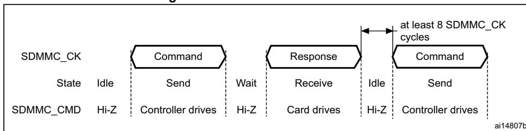
The command path operates in a half-duplex mode, so that commands and responses can either be sent or received. If the CPSM is not in the Send state, the SDIO_CMD output is in the Hi-Z state, as shown in Figure 239 on page 620 . Data on SDIO_CMD are synchronous with the rising edge of SDIO_CK. Table 95 shows the command format.
Table 95. Command format
| Bit position | Width | Value | Description |
|---|---|---|---|
| 47 | 1 | 0 | Start bit |
| 46 | 1 | 1 | Transmission bit |
| [45:40] | 6 | - | Command index |
| [39:8] | 32 | - | Argument |
| [7:1] | 7 | - | CRC7 |
| 0 | 1 | 1 | End bit |
- – Response: a response is a token that is sent from an addressed card (or synchronously from all connected cards for MMC V3.31 or previous), to the host as an answer to a previously received command. Responses are transferred serially on the CMD line.
The SDIO supports two response types. Both use CRC error checking:
- • 48 bit short response
- • 136 bit long response
Note: If the response does not contain a CRC (CMD1 response), the device driver must ignore the CRC failed status.
Table 96. Short response format
| Bit position | Width | Value | Description |
|---|---|---|---|
| 47 | 1 | 0 | Start bit |
| 46 | 1 | 0 | Transmission bit |
| [45:40] | 6 | - | Command index |
| [39:8] | 32 | - | Argument |
| [7:1] | 7 | - | CRC7(or 1111111) |
| 0 | 1 | 1 | End bit |
Table 97. Long response format
| Bit position | Width | Value | Description |
|---|---|---|---|
| 135 | 1 | 0 | Start bit |
| 134 | 1 | 0 | Transmission bit |
| [133:128] | 6 | 111111 | Reserved |
| [127:1] | 127 | - | CID or CSD (including internal CRC7) |
| 0 | 1 | 1 | End bit |
The command register contains the command index (six bits sent to a card) and the command type. These determine whether the command requires a response, and whether the response is 48 or 136 bits long (see Section 21.9.4 on page 655 ). The command path implements the status flags shown in Table 98 :
Table 98. Command path status flags
| Flag | Description |
|---|---|
| CMDREND | Set if response CRC is OK. |
| CCRCFAIL | Set if response CRC fails. |
| CMDSENT | Set when command (that does not require response) is sent |
| CTIMEOUT | Response timeout. |
| CMDACT | Command transfer in progress. |
The CRC generator calculates the CRC checksum for all bits before the CRC code. This includes the start bit, transmitter bit, command index, and command argument (or card status). The CRC checksum is calculated for the first 120 bits of CID or CSD for the long response format. Note that the start bit, transmitter bit and the six reserved bits are not used in the CRC calculation.
The CRC checksum is a 7-bit value:
Data path
The data path subunit transfers data to and from cards. Figure 240 shows a block diagram of the data path.
Figure 240. Data path
![Block diagram of the Data path subunit. The diagram shows a 'Data path' block containing 'Status flag', 'Control logic', and 'Data timer'. Below it, a 'Data FIFO' block contains 'Transmit' and 'Receive' sub-blocks. The 'Transmit' sub-block connects to a 'Shift register', which in turn connects to a 'CRC' block. The 'CRC' block outputs to 'SDMMC_Dout[7:0]'. The 'Shift register' also receives data from 'SDMMC_Din[7:0]' and sends it to the 'Receive' sub-block. The 'Status flag' and 'Control logic' are connected to the 'Data FIFO' and the 'Shift register'. The 'Data timer' is connected to the 'Control logic' and the 'Shift register'. The entire diagram is labeled 'ai14808b' in the bottom right corner.](/RM0368-STM32F401xB-C-401xD-E/2faa7a52e206c0ad2cc9bae318338bb4_img.jpg)
The card databus width can be programmed using the clock control register. If the 4-bit wide bus mode is enabled, data is transferred at four bits per clock cycle over all four data signals (SDIO_D[3:0]). If the 8-bit wide bus mode is enabled, data is transferred at eight bits per clock cycle over all eight data signals (SDIO_D[7:0]). If the wide bus mode is not enabled, only one bit per clock cycle is transferred over SDIO_D0.
Depending on the transfer direction (send or receive), the data path state machine (DPSM) moves to the Wait_S or Wait_R state when it is enabled:
- • Send: the DPSM moves to the Wait_S state. If there is data in the transmit FIFO, the DPSM moves to the Send state, and the data path subunit starts sending data to a card.
- • Receive: the DPSM moves to the Wait_R state and waits for a start bit. When it receives a start bit, the DPSM moves to the Receive state, and the data path subunit starts receiving data from a card.
Data path state machine (DPSM)
The DPSM operates at SDIO_CK frequency. Data on the card bus signals is synchronous to the rising edge of SDIO_CK. The DPSM has six states, as shown in Figure 241: Data path state machine (DPSM) .
Figure 241. Data path state machine (DPSM)
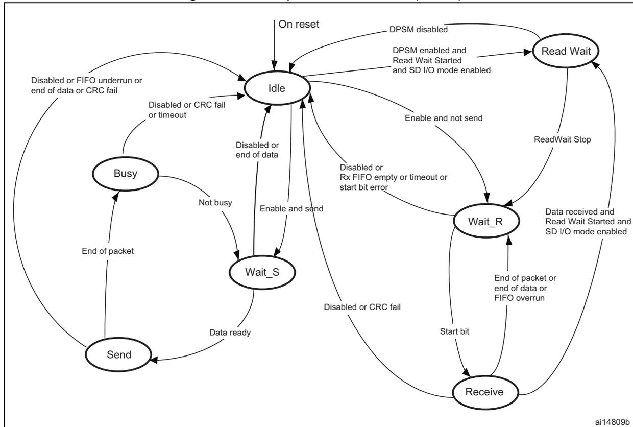
stateDiagram-v2
    [*] --> Idle : On reset
    Idle --> Idle : Disabled or FIFO underrun or end of data or CRC fail
    Idle --> Idle : Disabled or CRC fail or timeout
    Idle --> Idle : Disabled or end of data
    Idle --> Read Wait : DPSM disabled
    Idle --> Read Wait : DPSM enabled and Read Wait Started and SD I/O mode enabled
    Idle --> Wait_S : Enable and send
    Idle --> Wait_R : Enable and not send
    Idle --> Wait_R : Disabled or Rx FIFO empty or timeout or start bit error
    Idle --> Receive : Disabled or CRC fail
    Busy --> Idle : Not busy
    Busy --> Send : End of packet
    Wait_S --> Idle : Data ready
    Wait_S --> Send : Data ready
    Wait_R --> Idle : Disabled or CRC fail
    Wait_R --> Receive : Start bit
    Wait_R --> Idle : End of packet or end of data or FIFO overrun
    Read Wait --> Idle : ReadWait Stop
    Read Wait --> Wait_R : Data received and Read Wait Started and SD I/O mode enabled
- • Idle: the data path is inactive, and the SDIO_D[7:0] outputs are in Hi-Z. When the data control register is written and the enable bit is set, the DPSM loads the data counter with a new value and, depending on the data direction bit, moves to either the Wait_S or the Wait_R state.
- • Wait_R: if the data counter equals zero, the DPSM moves to the Idle state when the receive FIFO is empty. If the data counter is not zero, the DPSM waits for a start bit on SDIO_D. The DPSM moves to the Receive state if it receives a start bit before a timeout, and loads the data block counter. If it reaches a timeout before it detects a start bit, or a start bit error occurs, it moves to the Idle state and sets the timeout status flag.
- • Receive: serial data received from a card is packed in bytes and written to the data FIFO. Depending on the transfer mode bit in the data control register, the data transfer mode can be either block or stream:
- – In block mode, when the data block counter reaches zero, the DPSM waits until it receives the CRC code. If the received code matches the internally generated
CRC code, the DPSM moves to the Wait_R state. If not, the CRC fail status flag is set and the DPSM moves to the Idle state.
- – In stream mode, the DPSM receives data while the data counter is not zero. When the counter is zero, the remaining data in the shift register is written to the data FIFO, and the DPSM moves to the Wait_R state.
If a FIFO overrun error occurs, the DPSM sets the FIFO error flag and moves to the Idle state:
- • Wait_S: the DPSM moves to the Idle state if the data counter is zero. If not, it waits until the data FIFO empty flag is deasserted, and moves to the Send state.
Note: The DPSM remains in the Wait_S state for at least two clock periods to meet the \( N_{WR} \) timing requirements, where \( N_{WR} \) is the number of clock cycles between the reception of the card response and the start of the data transfer from the host.
- • Send: the DPSM starts sending data to a card. Depending on the transfer mode bit in the data control register, the data transfer mode can be either block or stream:
- – In block mode, when the data block counter reaches zero, the DPSM sends an internally generated CRC code and end bit, and moves to the Busy state.
- – In stream mode, the DPSM sends data to a card while the enable bit is high and the data counter is not zero. It then moves to the Idle state.
If a FIFO underrun error occurs, the DPSM sets the FIFO error flag and moves to the Idle state.
- • Busy: the DPSM waits for the CRC status flag:
- – If it does not receive a positive CRC status, it moves to the Idle state and sets the CRC fail status flag.
- – If it receives a positive CRC status, it moves to the Wait_S state if SDIO_D0 is not low (the card is not busy).
If a timeout occurs while the DPSM is in the Busy state, it sets the data timeout flag and moves to the Idle state.
The data timer is enabled when the DPSM is in the Wait_R or Busy state, and generates the data timeout error:
- – When transmitting data, the timeout occurs if the DPSM stays in the Busy state for longer than the programmed timeout period
- – When receiving data, the timeout occurs if the end of the data is not true, and if the DPSM stays in the Wait_R state for longer than the programmed timeout period.
- • Data: data can be transferred from the card to the host or vice versa. Data is transferred via the data lines. They are stored in a FIFO of 32 words, each word is 32 bits wide.
Table 99. Data token format
| Description | Start bit | Data | CRC16 | End bit |
|---|---|---|---|---|
| Block Data | 0 | - | yes | 1 |
| Stream Data | 0 | - | no | 1 |
Data FIFO
The data FIFO (first-in-first-out) subunit is a data buffer with a transmit and receive unit.
The FIFO contains a 32-bit wide, 32-word deep data buffer, and transmit and receive logic. Because the data FIFO operates in the APB2 clock domain (PCLK2), all signals from the subunits in the SDIO clock domain (SDIOCLK) are resynchronized.
Depending on the TXACT and RXACT flags, the FIFO can be disabled, transmit enabled, or receive enabled. TXACT and RXACT are driven by the data path subunit and are mutually exclusive:
- – The transmit FIFO refers to the transmit logic and data buffer when TXACT is asserted
- – The receive FIFO refers to the receive logic and data buffer when RXACT is asserted
- • Transmit FIFO:
Data can be written to the transmit FIFO through the APB2 interface when the SDIO is enabled for transmission.
The transmit FIFO is accessible via 32 sequential addresses. The transmit FIFO contains a data output register that holds the data word pointed to by the read pointer. When the data path subunit has loaded its shift register, it increments the read pointer and drives new data out.
If the transmit FIFO is disabled, all status flags are deasserted. The data path subunit asserts TXACT when it transmits data.
Table 100. Transmit FIFO status flags
| Flag | Description |
|---|---|
| TXFIFOF | Set to high when all 32 transmit FIFO words contain valid data. |
| TXFIFOE | Set to high when the transmit FIFO does not contain valid data. |
| TXFIFOHE | Set to high when 8 or more transmit FIFO words are empty. This flag can be used as a DMA request. |
| TXDAVL | Set to high when the transmit FIFO contains valid data. This flag is the inverse of the TXFIFOE flag. |
| TXUNDERR | Set to high when an underrun error occurs. This flag is cleared by writing to the SDIO Clear register. |
- • Receive FIFO
When the data path subunit receives a word of data, it drives the data on the write databus. The write pointer is incremented after the write operation completes. On the read side, the contents of the FIFO word pointed to by the current value of the read pointer is driven onto the read databus. If the receive FIFO is disabled, all status flags are deasserted, and the read and write pointers are reset. The data path subunit asserts RXACT when it receives data. Table 101 lists the receive FIFO status flags. The receive FIFO is accessible via 32 sequential addresses.
Table 101. Receive FIFO status flags| Flag | Description |
|---|---|
| RXFIFOF | Set to high when all 32 receive FIFO words contain valid data |
| RXFIFOE | Set to high when the receive FIFO does not contain valid data. |
| RXFIFOHF | Set to high when 8 or more receive FIFO words contain valid data. This flag can be used as a DMA request. |
| RXDAVL | Set to high when the receive FIFO is not empty. This flag is the inverse of the RXFIFOE flag. |
| RXOVERR | Set to high when an overrun error occurs. This flag is cleared by writing to the SDIO Clear register. |
21.3.2 SDIO APB2 interface
The APB2 interface generates the interrupt and DMA requests, and accesses the SDIO adapter registers and the data FIFO. It consists of a data path, register decoder, and interrupt/DMA logic.
SDIO interrupts
The interrupt logic generates an interrupt request signal that is asserted when at least one of the selected status flags is high. A mask register is provided to allow selection of the conditions that generate an interrupt. A status flag generates the interrupt request if a corresponding mask flag is set.
SDIO/DMA interface - procedure for data transfers between the SDIO and memory
In the example shown, the transfer is from the SDIO host controller to an MMC (512 bytes using CMD24 (WRITE_BLOCK). The SDIO FIFO is filled by data stored in a memory using the DMA controller.
- 1. Do the card identification process
- 2. Increase the SDIO_CK frequency
- 3. Select the card by sending CMD7
- 4. Configure the DMA2 as follows:
- a) Enable DMA2 controller and clear any pending interrupts.
- b) Program the DMA2_Stream3 or DMA2_Stream6 Channel4 source address register with the memory location's base address and DMA2_Stream3 or
- DMA2_Stream6 Channel4 destination address register with the SDIO_FIFO register address.
- c) Program DMA2_Stream3 or DMA2_Stream6 Channel4 control register (memory increment, not peripheral increment, peripheral and source width is word size).
- d) Program DMA2_Stream3 or DMA2_Stream6 Channel4 to select the peripheral as flow controller (set PFCTRL bit in DMA_S3CR or DMA_S6CR configuration register).
- e) Configure the incremental burst transfer to 4 beats (at least from peripheral side) in DMA2_Stream3 or DMA2_Stream6 Channel4.
- f) Enable DMA2_Stream3 or DMA2_Stream6 Channel4
- 5. Send CMD24 (WRITE_BLOCK) as follows:
- a) Program the SDIO data length register (SDIO data timer register should be already programmed before the card identification process).
- b) Program the SDIO argument register with the address location of the card where data is to be transferred.
- c) Program the SDIO command register: CmdIndex with 24 (WRITE_BLOCK); WaitResp with ‘1’ (SDIO card host waits for a response); CPSMEN with ‘1’ (SDIO card host enabled to send a command). Other fields are at their reset value.
- d) Wait for SDIO_STA[6] = CMDREND interrupt, then program the SDIO data control register: DTEN with ‘1’ (SDIO card host enabled to send data); DTDIR with ‘0’ (from controller to card); DTMODE with ‘0’ (block data transfer); DMAEN with ‘1’ (DMA enabled); DBLOCKSIZE with 0x9 (512 bytes). Other fields are don’t care.
- e) Wait for SDIO_STA[10] = DBCKEND.
- 6. Check that no channels are still enabled by polling the DMA Enabled Channel Status register.
21.4 Card functional description
21.4.1 Card identification mode
While in card identification mode the host resets all cards, validates the operation voltage range, identifies cards and sets a relative card address (RCA) for each card on the bus. All data communications in the card identification mode use the command line (CMD) only.
21.4.2 Card reset
The
GO_IDLE_STATE
command (CMD0) is the software reset command and it puts the MultiMediaCard and SD memory in the
Idle
state. The
IO_RW_DIRECT
command (CMD52) resets the SD I/O card. After power-up or CMD0, all cards output bus drivers are in the high-impedance state and the cards are initialized with a default relative card address (RCA=0x0001) and with a default driver stage register setting (lowest speed, highest driving current capability).
21.4.3 Operating voltage range validation
All cards can communicate with the SDIO card host using any operating voltage within the specification range. The supported minimum and maximum \( V_{DD} \) values are defined in the operation conditions register (OCR) on the card.
Cards that store the card identification number (CID) and card specific data (CSD) in the payload memory are able to communicate this information only under data-transfer
\(
V_{DD}
\)
conditions. When the SDIO card host module and the card have incompatible
\(
V_{DD}
\)
ranges, the card is not able to complete the identification cycle and cannot send CSD data. For this purpose, the special commands,
SEND_OP_COND
(CMD1),
SD_APP_OP_COND
(ACMD41 for SD Memory), and
IO_SEND_OP_COND
(CMD5 for SD I/O), are designed to provide a mechanism to identify and reject cards that do not match the
\(
V_{DD}
\)
range desired by the SDIO card host. The SDIO card host sends the required
\(
V_{DD}
\)
voltage window as the operand of these commands. Cards that cannot perform data transfer in the specified range disconnect from the bus and go to the inactive state.
By using these commands without including the voltage range as the operand, the SDIO card host can query each card and determine the common voltage range before placing out-of-range cards in the inactive state. This query is used when the SDIO card host is able to select a common voltage range or when the user requires notification that cards are not usable.
21.4.4 Card identification process
The card identification process differs for MultiMediaCards and SD cards. For MultiMediaCard cards, the identification process starts at clock rate \( F_{od} \) . The SDIO_CMD line output drivers are open-drain and allow parallel card operation during this process. The registration process is accomplished as follows:
- 1. The bus is activated.
- 2. The SDIO card host broadcasts
SEND_OP_COND(CMD1) to receive operation conditions. - 3. The response is the wired AND operation of the operation condition registers from all cards.
- 4. Incompatible cards are placed in the inactive state.
- 5. The SDIO card host broadcasts
ALL_SEND_CID(CMD2) to all active cards. - 6. The active cards simultaneously send their CID numbers serially. Cards with outgoing CID bits that do not match the bits on the command line stop transmitting and must wait for the next identification cycle. One card successfully transmits a full CID to the SDIO card host and enters the Identification state.
- 7. The SDIO card host issues
SET_RELATIVE_ADDR(CMD3) to that card. This new address is called the relative card address (RCA); it is shorter than the CID and addresses the card. The assigned card changes to the Standby state, it does not react to further identification cycles, and its output switches from open-drain to push-pull. - 8. The SDIO card host repeats steps 5 through 7 until it receives a timeout condition.
For the SD card, the identification process starts at clock rate \( F_{od} \) , and the SDIO_CMD line output drives are push-pull drivers instead of open-drain. The registration process is accomplished as follows:
- 1. The bus is activated.
- 2. The SDIO card host broadcasts
SD_APP_OP_COND(ACMD41). - 3. The cards respond with the contents of their operation condition registers.
- 4. The incompatible cards are placed in the inactive state.
- 5. The SDIO card host broadcasts
ALL_SEND_CID(CMD2) to all active cards. - 6. The cards send back their unique card identification numbers (CIDs) and enter the Identification state.
- 7. The SDIO card host issues
SET_RELATIVE_ADDR(CMD3) to an active card with an address. This new address is called the relative card address (RCA); it is shorter than the CID and addresses the card. The assigned card changes to the Standby state. The SDIO card host can reissue this command to change the RCA. The RCA of the card is the last assigned value. - 8. The SDIO card host repeats steps 5 through 7 with all active cards.
For the SD I/O card, the registration process is accomplished as follows:
- 1. The bus is activated.
- 2. The SDIO card host sends
IO_SEND_OP_COND(CMD5). - 3. The cards respond with the contents of their operation condition registers.
- 4. The incompatible cards are set to the inactive state.
- 5. The SDIO card host issues
SET_RELATIVE_ADDR(CMD3) to an active card with an address. This new address is called the relative card address (RCA); it is shorter than the CID and addresses the card. The assigned card changes to the Standby state. The SDIO card host can reissue this command to change the RCA. The RCA of the card is the last assigned value.
21.4.5 Block write
During block write (CMD24 - 27) one or more blocks of data are transferred from the host to the card with a CRC appended to the end of each block by the host. A card supporting block write is always able to accept a block of data defined by
WRITE_BL_LEN
. If the CRC fails, the card indicates the failure on the
SDIO_D
line and the transferred data are discarded and not written, and all further transmitted blocks (in multiple block write mode) are ignored.
If the host uses partial blocks whose accumulated length is not block aligned and, block misalignment is not allowed (CSD parameter
WRITE_BLK_MISALIGN
is not set), the card detects the block misalignment error before the beginning of the first misaligned block. (
ADDRESS_ERROR
error bit is set in the status register). The write operation is also aborted if the host tries to write over a write-protected area. In this case, however, the card sets the
WP_VIOLATION
bit.
Programming of the CID and CSD registers does not require a previous block length setting. The transferred data is also CRC protected. If a part of the CSD or CID register is stored in ROM, then this unchangeable part must match the corresponding part of the receive buffer. If this match fails, then the card reports an error and does not change any register contents. Some cards may require long and unpredictable times to write a block of data. After receiving a block of data and completing the CRC check, the card begins writing and holds the
SDIO_D
line low if its write buffer is full and unable to accept new data from a new
WRITE_BLOCK
command. The host may poll the status of the card with a
SEND_STATUS
command (CMD13) at any time, and the card responds with its status. The
READY_FOR_DATA
status bit indicates whether the card can accept new data or whether the write process is still in progress. The host may deselect the card by issuing CMD7 (to
select a different card), which places the card in the Disconnect state and release the SDIO_D line(s) without interrupting the write operation. When selecting the card again, it reactivates busy indication by pulling SDIO_D to low if programming is still in progress and the write buffer is unavailable.
21.4.6 Block read
In Block read mode the basic unit of data transfer is a block whose maximum size is defined in the CSD (READ_BL_LEN). If READ_BL_PARTIAL is set, smaller blocks whose start and end addresses are entirely contained within one physical block (as defined by READ_BL_LEN) may also be transmitted. A CRC is appended to the end of each block, ensuring data transfer integrity. CMD17 (READ_SINGLE_BLOCK) initiates a block read and after completing the transfer, the card returns to the Transfer state.
CMD18 (READ_MULTIPLE_BLOCK) starts a transfer of several consecutive blocks.
The host can abort reading at any time, within a multiple block operation, regardless of its type. Transaction abort is done by sending the stop transmission command.
If the card detects an error (for example, out of range, address misalignment or internal error) during a multiple block read operation (both types) it stops the data transmission and remains in the data state. The host must then abort the operation by sending the stop transmission command. The read error is reported in the response to the stop transmission command.
If the host sends a stop transmission command after the card transmits the last block of a multiple block operation with a predefined number of blocks, it is responded to as an illegal command, since the card is no longer in the data state. If the host uses partial blocks whose accumulated length is not block-aligned and block misalignment is not allowed, the card detects a block misalignment error condition at the beginning of the first misaligned block (ADDRESS_ERROR error bit is set in the status register).
21.4.7 Stream access, stream write and stream read (MultiMediaCard only)
In stream mode, data is transferred in bytes and no CRC is appended at the end of each block.
Stream write (MultiMediaCard only)
WRITE_DAT_UNTIL_STOP (CMD20) starts the data transfer from the SDIO card host to the card, beginning at the specified address and continuing until the SDIO card host issues a stop command. When partial blocks are allowed (CSD parameter WRITE_BL_PARTIAL is set), the data stream can start and stop at any address within the card address space, otherwise it can only start and stop at block boundaries. Because the amount of data to be transferred is not determined in advance, a CRC cannot be used. When the end of the memory range is reached while sending data and no stop command is sent by the SD card host, any additional transferred data are discarded.
The maximum clock frequency for a stream write operation is given by the following equation fields of the card-specific data register:
- • Maximumspeed = maximum write frequency
- • TRANSPEED = maximum data transfer rate
- • writeblen = maximum write data block length
- • NSAC = data read access time 2 in CLK cycles
- • TAAC = data read access time 1
- • R2WFACTOR = write speed factor
If the host attempts to use a higher frequency, the card may not be able to process the data and stop programming, set the OVERRUN error bit in the status register, and while ignoring all further data transfer, wait (in the receive data state) for a stop command. The write operation is also aborted if the host tries to write over a write-protected area. In this case, however, the card sets the WP_VIOLATION bit.
Stream read (MultiMediaCard only)
READ_DAT_UNTIL_STOP (CMD11) controls a stream-oriented data transfer.
This command instructs the card to send its data, starting at a specified address, until the SDIO card host sends STOP_TRANSMISSION (CMD12). The stop command has an execution delay due to the serial command transmission and the data transfer stops after the end bit of the stop command. When the end of the memory range is reached while sending data and no stop command is sent by the SDIO card host, any subsequent data sent are considered undefined.
The maximum clock frequency for a stream read operation is given by the following equation and uses fields of the card specific data register.
- • Maximumspeed = maximum read frequency
- • TRANSPEED = maximum data transfer rate
- • readblen = maximum read data block length
- • writeblen = maximum write data block length
- • NSAC = data read access time 2 in CLK cycles
- • TAAC = data read access time 1
- • R2WFACTOR = write speed factor
If the host attempts to use a higher frequency, the card is not able to sustain data transfer. If this happens, the card sets the UNDERRUN error bit in the status register, aborts the transmission and waits in the data state for a stop command.
21.4.8 Erase: group erase and sector erase
The erasable unit of the MultiMediaCard is the erase group. The erase group is measured in write blocks, which are the basic writable units of the card. The size of the erase group is a card-specific parameter and defined in the CSD.
The host can erase a contiguous range of Erase Groups. Starting the erase process is a three-step sequence.
First the host defines the start address of the range using the
ERASE_GROUP_START
(CMD35) command, next it defines the last address of the range using the
ERASE_GROUP_END
(CMD36) command and, finally, it starts the erase process by issuing the
ERASE
(CMD38) command. The address field in the erase commands is an Erase Group address in byte units. The card ignores all LSBs below the Erase Group size, effectively rounding the address down to the Erase Group boundary.
If an erase command is received out of sequence, the card sets the
ERASE_SEQ_ERROR
bit in the status register and resets the whole sequence.
If an out-of-sequence (neither of the erase commands, except
SEND_STATUS
) command received, the card sets the
ERASE_RESET
status bit in the status register, resets the erase sequence and executes the last command.
If the erase range includes write protected blocks, they are left intact and only unprotected blocks are erased. The
WP_ERASE_SKIP
status bit in the status register is set.
The card indicates that an erase is in progress by holding
SDIO_D
low. The actual erase time may be quite long, and the host may issue CMD7 to deselect the card.
21.4.9 Wide bus selection or deselection
Wide bus (4-bit bus width) operation mode is selected or deselected using
SET_BUS_WIDTH
(ACMD6). The default bus width after power-up or
GO_IDLE_STATE
(CMD0) is 1 bit.
SET_BUS_WIDTH
(ACMD6) is only valid in a transfer state, which means that the bus width can be changed only after a card is selected by
SELECT/DESELECT_CARD
(CMD7).
21.4.10 Protection management
Three write protection methods for the cards are supported in the SDIO card host module:
- 1. internal card write protection (card responsibility)
- 2. mechanical write protection switch (SDIO card host module responsibility only)
- 3. password-protected card lock operation
Internal card write protection
Card data can be protected against write and erase. By setting the permanent or temporary write-protect bits in the CSD, the entire card can be permanently write-protected by the manufacturer or content provider. For cards that support write protection of groups of sectors by setting the
WP_GRP_ENABLE
bit in the CSD, portions of the data can be protected, and the write protection can be changed by the application. The write protection is in units of
WP_GRP_SIZE
sectors as specified in the CSD. The
SET_WRITE_PROT
and
CLR_WRITE_PROT
commands control the protection of the addressed group. The
SEND_WRITE_PROT
command is similar to a single block read command. The card sends a data block containing 32 write protection bits (representing 32 write protect groups starting
at the specified address) followed by 16 CRC bits. The address field in the write protect commands is a group address in byte units.
The card ignores all LSBs below the group size.
Mechanical write protect switch
A mechanical sliding tab on the side of the card allows the user to set or clear the write protection on a card. When the sliding tab is positioned with the window open, the card is write-protected, and when the window is closed, the card contents can be changed. A matched switch on the socket side indicates to the SDIO card host module that the card is write-protected. The SDIO card host module is responsible for protecting the card. The position of the write protect switch is unknown to the internal circuitry of the card.
Password protect
The password protection feature enables the SDIO card host module to lock and unlock a card with a password. The password is stored in the 128-bit PWD register and its size is set in the 8-bit PWD_LEN register. These registers are nonvolatile so that a power cycle does not erase them. Locked cards respond to and execute certain commands. This means that the SDIO card host module is allowed to reset, initialize, select, and query for status, however it is not allowed to access data on the card. When the password is set (as indicated by a nonzero value of PWD_LEN), the card is locked automatically after power-up. As with the CSD and CID register write commands, the lock/unlock commands are available in the transfer state only. In this state, the command does not include an address argument and the card must be selected before using it. The card lock/unlock commands have the structure and bus transaction types of a regular single-block write command. The transferred data block includes all of the required information for the command (the password setting mode, the PWD itself, and card lock/unlock). The command data block size is defined by the SDIO card host module before it sends the card lock/unlock command, and has the structure shown in Table 115 .
The bit settings are as follows:
- • ERASE: setting it forces an erase operation. All other bits must be zero, and only the command byte is sent
- • LOCK_UNLOCK: setting it locks the card. LOCK_UNLOCK can be set simultaneously with SET_PWD, however not with CLR_PWD
- • CLR_PWD: setting it clears the password data
- • SET_PWD: setting it saves the password data to memory
- • PWD_LEN: it defines the length of the password in bytes
- • PWD: the password (new or currently used, depending on the command)
The following sections list the command sequences to set/reset a password, lock/unlock the card, and force an erase.
Setting the password
- 1. Select a card (SELECT/DESELECT_CARD, CMD7), if none is already selected.
- 2. Define the block length (SET_BLOCKLEN, CMD16) to send, given by the 8-bit card lock/unlock mode, the 8-bit PWD_LEN, and the number of bytes of the new password.
When a password replacement is done, the block size must take into account that both the old and the new passwords are sent with the command.
- 3. Send LOCK/UNLOCK (CMD42) with the appropriate data block size on the data line including the 16-bit CRC. The data block indicates the mode ( SET_PWD = 1 ), the length ( PWD_LEN ), and the password ( PWD ) itself. When a password replacement is done, the length value ( PWD_LEN ) includes the length of both passwords, the old and the new one, and the PWD field includes the old password (currently used) followed by the new password.
- 4. When the password is matched, the new password and its size are saved into the PWD and PWD_LEN fields, respectively. When the old password sent does not correspond (in size and/or content) to the expected password, the LOCK_UNLOCK_FAILED error bit is set in the card status register, and the password is not changed.
The password length field ( PWD_LEN ) indicates whether a password is currently set. When this field is nonzero, there is a password set and the card locks itself after power-up. It is possible to lock the card immediately in the current power session by setting the LOCK_UNLOCK bit (while setting the password) or sending an additional command for card locking.
Resetting the password
- 1. Select a card ( SELECT/DESELECT_CARD , CMD7), if none is already selected.
- 2. Define the block length ( SET_BLOCKLEN , CMD16) to send, given by the 8-bit card lock/unlock mode, the 8-bit PWD_LEN , and the number of bytes in the currently used password.
- 3. Send LOCK/UNLOCK (CMD42) with the appropriate data block size on the data line including the 16-bit CRC. The data block indicates the mode ( CLR_PWD = 1 ), the length ( PWD_LEN ) and the password ( PWD ) itself. The LOCK_UNLOCK bit is ignored.
- 4. When the password is matched, the PWD field is cleared and PWD_LEN is set to 0. When the password sent does not correspond (in size and/or content) to the expected password, the LOCK_UNLOCK_FAILED error bit is set in the card status register, and the password is not changed.
Locking a card
- 1. Select a card ( SELECT/DESELECT_CARD , CMD7), if none is already selected.
- 2. Define the block length ( SET_BLOCKLEN , CMD16) to send, given by the 8-bit card lock/unlock mode (byte 0 in Table 115 ), the 8-bit PWD_LEN , and the number of bytes of the current password.
- 3. Send LOCK/UNLOCK (CMD42) with the appropriate data block size on the data line including the 16-bit CRC. The data block indicates the mode ( LOCK_UNLOCK = 1 ), the length ( PWD_LEN ), and the password ( PWD ) itself.
- 4. When the password is matched, the card is locked and the CARD_IS_LOCKED status bit is set in the card status register. When the password sent does not correspond (in size and/or content) to the expected password, the LOCK_UNLOCK_FAILED error bit is set in the card status register, and the lock fails.
It is possible to set the password and to lock the card in the same sequence. In this case, the SDIO card host module performs all the required steps for setting the password (see Setting the password on page 633 ), however it is necessary to set the LOCK_UNLOCK bit in Step 3 when the new password command is sent.
When the password is previously set (PWD_LEN is not 0), the card is locked automatically after power-on reset. An attempt to lock a locked card or to lock a card that does not have a password fails and the LOCK_UNLOCK_FAILED error bit is set in the card status register.
Unlocking the card
- 1. Select a card (SELECT/DESELECT_CARD, CMD7), if none is already selected.
- 2. Define the block length (SET_BLOCKLEN, CMD16) to send, given by the 8-bit cardlock/unlock mode (byte 0 in Table 115 ), the 8-bit PWD_LEN, and the number of bytes of the current password.
- 3. Send LOCK/UNLOCK (CMD42) with the appropriate data block size on the data line including the 16-bit CRC. The data block indicates the mode (LOCK_UNLOCK = 0), the length (PWD_LEN), and the password (PWD) itself.
- 4. When the password is matched, the card is unlocked and the CARD_IS_LOCKED status bit is cleared in the card status register. When the password sent is not correct in size and/or content and does not correspond to the expected password, the LOCK_UNLOCK_FAILED error bit is set in the card status register, and the card remains locked.
The unlocking function is only valid for the current power session. When the PWD field is not clear, the card is locked automatically on the next power-up.
An attempt to unlock an unlocked card fails and the LOCK_UNLOCK_FAILED error bit is set in the card status register.
Forcing erase
If the user has forgotten the password (PWD content), it is possible to access the card after clearing all the data on the card. This forced erase operation erases all card data and all password data.
- 1. Select a card (SELECT/DESELECT_CARD, CMD7), if none is already selected.
- 2. Set the block length (SET_BLOCKLEN, CMD16) to 1 byte. Only the 8-bit card lock/unlock byte (byte 0 in Table 115 ) is sent.
- 3. Send LOCK/UNLOCK (CMD42) with the appropriate data byte on the data line including the 16-bit CRC. The data block indicates the mode (ERASE = 1). All other bits must be zero.
- 4. When the ERASE bit is the only bit set in the data field, all card contents are erased, including the PWD and PWD_LEN fields, and the card is no longer locked. When any other bits are set, the LOCK_UNLOCK_FAILED error bit is set in the card status register and the card retains all of its data, and remains locked.
An attempt to use a force erase on an unlocked card fails and the LOCK_UNLOCK_FAILED error bit is set in the card status register.
21.4.11 Card status register
The response format R1 contains a 32-bit field named card status. This field is intended to transmit the card status information (which may be stored in a local status register) to the host. If not specified otherwise, the status entries are always related to the previously issued command.
Table 102 defines the different entries of the status. The type and clear condition fields in the table are abbreviated as follows:
Type:
- • E: error bit
- • S: status bit
- • R: detected and set for the actual command response
- • X: detected and set during command execution. The SDIO card host must poll the card by issuing the status command to read these bits.
Clear condition:
- • A: according to the card current state
- • B: always related to the previous command. Reception of a valid command clears it (with a delay of one command)
- • C: clear by read
Table 102. Card status
| Bits | Identifier | Type | Value | Description | Clear condition |
|---|---|---|---|---|---|
| 31 | ADDRESS_OUT_OF_RANGE | E R X | '0'= no error '1'= error | The command address argument was out of the allowed range for this card. A multiple block or stream read/write operation is (although started in a valid address) attempting to read or write beyond the card capacity. | C |
| 30 | ADDRESS_MISALIGN | - | '0'= no error '1'= error | The commands address argument (in accordance with the currently set block length) positions the first data block misaligned to the card physical blocks. A multiple block read/write operation (although started with a valid address/block-length combination) is attempting to read or write a data block which is not aligned with the physical blocks of the card. | C |
| 29 | BLOCK_LEN_ERROR | - | '0'= no error '1'= error | Either the argument of a SET_BLOCKLEN command exceeds the maximum value allowed for the card, or the previously defined block length is illegal for the current command (e.g. the host issues a write command, the current block length is smaller than the maximum allowed value for the card and it is not allowed to write partial blocks) | C |
| 28 | ERASE_SEQ_ERROR | - | '0'= no error '1'= error | An error in the sequence of erase commands occurred. | C |
| 27 | ERASE_PARAM | E X | '0'= no error '1'= error | An invalid selection of erase groups for erase occurred. | C |
| 26 | WP_VIOLATION | E X | '0'= no error '1'= error | Attempt to program a write-protected block. | C |
Table 102. Card status (continued)
| Bits | Identifier | Type | Value | Description | Clear condition |
|---|---|---|---|---|---|
| 25 | CARD_IS_LOCKED | S R | '0' = card unlocked '1' = card locked | When set, signals that the card is locked by the host | A |
| 24 | LOCK_UNLOCK_FAILED | E X | '0' = no error '1' = error | Set when a sequence or password error has been detected in lock/unlock card command | C |
| 23 | COM_CRC_ERROR | E R | '0' = no error '1' = error | The CRC check of the previous command failed. | B |
| 22 | ILLEGAL_COMMAND | E R | '0' = no error '1' = error | Command not legal for the card state | B |
| 21 | CARD_ECC_FAILED | E X | '0' = success '1' = failure | Card internal ECC was applied but failed to correct the data. | C |
| 20 | CC_ERROR | E R | '0' = no error '1' = error | (Undefined by the standard) A card error occurred, which is not related to the host command. | C |
| 19 | ERROR | E X | '0' = no error '1' = error | (Undefined by the standard) A generic card error related to the (and detected during) execution of the last host command (e.g. read or write failures). | C |
| 18 | Reserved | ||||
| 17 | Reserved | ||||
| 16 | CID/CSD_OVERWRITE | E X | '0' = no error '1' = error | Can be either of the following errors: – The CID register has already been written and cannot be overwritten – The read-only section of the CSD does not match the card contents – An attempt to reverse the copy (set as original) or permanent WP (unprotected) bits was made | C |
| 15 | WP_ERASE_SKIP | E X | '0' = not protected '1' = protected | Set when only partial address space was erased due to existing write | C |
| 14 | CARD_ECC_DISABLED | S X | '0' = enabled '1' = disabled | The command has been executed without using the internal ECC. | A |
| 13 | ERASE_RESET | - | '0' = cleared '1' = set | An erase sequence was cleared before executing because an out of erase sequence command was received (commands other than CMD35, CMD36, CMD38 or CMD13) | C |
Table 102. Card status (continued)
| Bits | Identifier | Type | Value | Description | Clear condition |
|---|---|---|---|---|---|
| 12:9 | CURRENT_STATE | S R | 0 = Idle 1 = Ready 2 = Ident 3 = Stby 4 = Tran 5 = Data 6 = Rcv 7 = Prg 8 = Dis 9 = Btst 10-15 = reserved | The state of the card when receiving the command. If the command execution causes a state change, it is visible to the host in the response on the next command. The four bits are interpreted as a binary number between 0 and 15. | B |
| 8 | READY_FOR_DATA | S R | '0' = not ready '1' = ready | Corresponds to buffer empty signalling on the bus | - |
| 7 | SWITCH_ERROR | E X | '0' = no error '1' = switch error | If set, the card did not switch to the expected mode as requested by the SWITCH command | B |
| 6 | Reserved | ||||
| 5 | APP_CMD | S R | '0' = Disabled '1' = Enabled | The card expects ACMD, or an indication that the command has been interpreted as ACMD | C |
| 4 | Reserved for SD I/O Card | ||||
| 3 | AKE_SEQ_ERROR | E R | '0' = no error '1' = error | Error in the sequence of the authentication process | C |
| 2 | Reserved for application specific commands | ||||
| 1 | Reserved for manufacturer test mode | ||||
| 0 | |||||
21.4.12 SD status register
The SD status contains status bits that are related to the SD memory card proprietary features and may be used for future application-specific usage. The size of the SD Status is one data block of 512 bits. The contents of this register are transmitted to the SDIO card host if ACMD13 is sent (CMD55 followed with CMD13). ACMD13 can be sent to a card in transfer state only (card is selected).
Table 103 defines the different entries of the SD status register. The type and clear condition fields in the table are abbreviated as follows:
Type:
- • E: error bit
- • S: status bit
- • R: detected and set for the actual command response
- • X: detected and set during command execution. The SDIO card Host must poll the card by issuing the status command to read these bits
Clear condition:
- • A: according to the card current state
- • B: always related to the previous command. Reception of a valid command clears it (with a delay of one command)
- • C: clear by read
Table 103. SD status
| Bits | Identifier | Type | Value | Description | Clear condition |
|---|---|---|---|---|---|
| 511: 510 | DAT_BUS_WIDTH | S R | '00'= 1 (default) '01'= reserved '10'= 4 bit width '11'= reserved | Shows the currently defined databus width that was defined by SET_BUS_WIDTH command | A |
| 509 | SECURED_MODE | S R | '0'= Not in the mode '1'= In Secured Mode | Card is in Secured Mode of operation (refer to the “SD Security Specification”). | A |
| 508: 496 | Reserved | ||||
| 495: 480 | SD_CARD_TYPE | S R | '00xxh'= SD Memory Cards as defined in Physical Spec Ver1.01-2.00 ('x'= don't care). The following cards are currently defined: '0000'= Regular SD RD/WR Card. '0001'= SD ROM Card | In the future, the 8 LSBs are used to define different variations of an SD memory card (each bit defines different SD types). The 8 MSBs are used to define SD Cards that do not comply with current SD physical layer specification. | A |
| 479: 448 | SIZE_OF_PROTECTED_AREA | S R | Size of protected area (See below) | (See below) | A |
| 447: 440 | SPEED_CLASS | S R | Speed Class of the card (See below) | (See below) | A |
| 439: 432 | PERFORMANCE_MOVE | S R | Performance of move indicated by 1 [MB/s] step. (See below) | (See below) | A |
| 431:428 | AU_SIZE | S R | Size of AU (See below) | (See below) | A |
| 427:424 | Reserved | ||||
| 423:408 | ERASE_SIZE | S R | Number of AUs to be erased at a time | (See below) | A |
| 407:402 | ERASE_TIMEOUT | S R | Timeout value for erasing areas specified by UNIT_OF_ERASE_AU | (See below) | A |
| 401:400 | ERASE_OFFSET | S R | Fixed offset value added to erase time. | (See below) | A |
| 399:312 | Reserved | ||||
| 311:0 | Reserved for Manufacturer | ||||
SIZE_OF_PROTECTED_AREA
Setting this field differs between standard- and high-capacity cards. In the case of a standard-capacity card, the capacity of protected area is calculated as follows:
Protected area = \( SIZE\_OF\_PROTECTED\_AREA\_ * \ MULT * \ BLOCK\_LEN \) .
\( SIZE\_OF\_PROTECTED\_AREA \) is specified by the unit in \( MULT * BLOCK\_LEN \) .
In the case of a high-capacity card, the capacity of protected area is specified in this field:
Protected area = \( SIZE\_OF\_PROTECTED\_AREA \)
\( SIZE\_OF\_PROTECTED\_AREA \) is specified by the unit in bytes.
SPEED_CLASS
This 8-bit field indicates the speed class and the value can be calculated by \( P_W/2 \) (where \( P_W \) is the write performance).
Table 104. Speed class code field
| SPEED_CLASS | Value definition |
|---|---|
| 00h | Class 0 |
| 01h | Class 2 |
| 02h | Class 4 |
| 03h | Class 6 |
| 04h – FFh | Reserved |
PERFORMANCE_MOVE
This 8-bit field indicates \( P_m \) (performance move) and the value can be set by 1 [MB/sec] steps. If the card does not move used RUs (recording units), \( P_m \) should be considered as infinity. Setting the field to FFh means infinity.
Table 105. Performance move field
| PERFORMANCE_MOVE | Value definition |
|---|---|
| 00h | Not defined |
| 01h | 1 [MB/sec] |
| 02h | 02h 2 [MB/sec] |
| ----- | ----- |
| FEh | 254 [MB/sec] |
| FFh | Infinity |
AU_SIZE
This 4-bit field indicates the AU size and the value can be selected in the power of 2 base from 16 KB.
Table 106. AU_SIZE field
| AU_SIZE | Value definition |
|---|---|
| 00h | Not defined |
| 01h | 16 KB |
| 02h | 32 KB |
| 03h | 64 KB |
| 04h | 128 KB |
| 05h | 256 KB |
| 06h | 512 KB |
| 07h | 1 MB |
| 08h | 2 MB |
| 09h | 4 MB |
| Ah – Fh | Reserved |
The maximum AU size, which depends on the card capacity, is defined in Table 107 . The card can be set to any AU size between RU size and maximum AU size.
Table 107. Maximum AU size
| Capacity | 16 MB-64 MB | 128 MB-256 MB | 512 MB | 1 GB-32 GB |
|---|---|---|---|---|
| Maximum AU Size | 512 KB | 1 MB | 2 MB | 4 MB |
ERASE_SIZE
This 16-bit field indicates NERASE. When NERASE numbers of AUs are erased, the timeout value is specified by ERASE_TIMEOUT (Refer to ERASE_TIMEOUT ). The host should determine the proper number of AUs to be erased in one operation so that the host can show the progress of the erase operation. If this field is set to 0, the erase timeout calculation is not supported.
Table 108. Erase size field
| ERASE_SIZE | Value definition |
|---|---|
| 0000h | Erase timeout calculation is not supported. |
| 0001h | 1 AU |
| 0002h | 2 AU |
| 0003h | 3 AU |
| ---------- | ---------- |
| FFFFh | 65535 AU |
ERASE_TIMEOUT
This 6-bit field indicates TERASE and the value indicates the erase timeout from offset when multiple AUs are being erased as specified by ERASE_SIZE. The range of ERASE_TIMEOUT can be defined as up to 63 seconds and the card manufacturer can choose any combination of ERASE_SIZE and ERASE_TIMEOUT depending on the implementation. Determining ERASE_TIMEOUT determines the ERASE_SIZE.
Table 109. Erase timeout field
| ERASE_TIMEOUT | Value definition |
|---|---|
| 00 | Erase timeout calculation is not supported. |
| 01 | 1 [sec] |
| 02 | 2 [sec] |
| 03 | 3 [sec] |
| ----- | ----- |
| 63 | 63 [sec] |
ERASE_OFFSET
This 2-bit field indicates TOFFSET and one of four values can be selected. This field is meaningless if the ERASE_SIZE and ERASE_TIMEOUT fields are set to 0.
Table 110. Erase offset field
| ERASE_OFFSET | Value definition |
|---|---|
| 0h | 0 [sec] |
| 1h | 1 [sec] |
| 2h | 2 [sec] |
| 3h | 3 [sec] |
21.4.13 SD I/O mode
SD I/O interrupts
To allow the SD I/O card to interrupt the MultiMediaCard/SD module, an interrupt function is available on a pin on the SD interface. Pin 8, used as SDIO_D1 when operating in the 4-bit SD mode, signals the cards interrupt to the MultiMediaCard/SD module. The use of the interrupt is optional for each card or function within a card. The SD I/O interrupt is level-sensitive, which means that the interrupt line must be held active (low) until it is either recognized and acted upon by the MultiMediaCard/SD module or deasserted due to the end of the interrupt period. After the MultiMediaCard/SD module has serviced the interrupt, the interrupt status bit is cleared via an I/O write to the appropriate bit in the SD I/O card's internal registers. The interrupt output of all SD I/O cards is active low and the application must provide external pull-up resistors on all data lines (SDIO_D[3:0]). The MultiMediaCard/SD module samples the level of pin 8 (SDIO_D/IRQ) into the interrupt detector only during the interrupt period. At all other times, the MultiMediaCard/SD module ignores this value.
The interrupt period is applicable for both memory and I/O operations. The definition of the interrupt period for operations with single blocks is different from the definition for multiple-block data transfers.
SD I/O suspend and resume
Within a multifunction SD I/O or a card with both I/O and memory functions, there are multiple devices (I/O and memory) that share access to the MMC/SD bus. To share access to the MMC/SD module among multiple devices, SD I/O and combo cards optionally implement the concept of suspend/resume. When a card supports suspend/resume, the MMC/SD module can temporarily halt a data transfer operation to one function or memory (suspend) to free the bus for a higher-priority transfer to a different function or memory. After this higher-priority transfer is complete, the original transfer is resumed (restarted) where it left off. Support of suspend/resume is optional on a per-card basis. To perform the suspend/resume operation on the MMC/SD bus, the MMC/SD module performs the following steps:
- 1. Determines the function currently using the SDIO_D [3:0] line(s)
- 2. Requests the lower-priority or slower transaction to suspend
- 3. Waits for the transaction suspension to complete
- 4. Begins the higher-priority transaction
- 5. Waits for the completion of the higher priority transaction
- 6. Restores the suspended transaction
SD I/O ReadWait
The optional ReadWait (RW) operation is defined only for the SD 1-bit and 4-bit modes. The ReadWait operation allows the MMC/SD module to signal a card that it is reading multiple registers (IO_RW_EXTENDED, CMD53) to temporarily stall the data transfer while allowing the MMC/SD module to send commands to any function within the SD I/O device. To determine when a card supports the ReadWait protocol, the MMC/SD module must test capability bits in the internal card registers. The timing for ReadWait is based on the interrupt period.
21.4.14 Commands and responses
Application-specific and general commands
The SD card host module system is designed to provide a standard interface for a variety of applications types. In this environment, there is a need for specific customer/application features. To implement these features, two types of generic commands are defined in the standard: application-specific commands (ACMD) and general commands (GEN_CMD).
When the card receives the APP_CMD (CMD55) command, the card expects the next command to be an application-specific command. ACMDs have the same structure as regular MultiMediaCard commands and can have the same CMD number. The card recognizes it as ACMD because it appears after APP_CMD (CMD55). When the command immediately following the APP_CMD (CMD55) is not a defined application-specific command, the standard command is used. For example, when the card has a definition for SD_STATUS (ACMD13), and receives CMD13 immediately following APP_CMD (CMD55), this is interpreted as SD_STATUS (ACMD13). However, when the card receives CMD7 immediately following APP_CMD (CMD55) and the card does not have a definition for ACMD7, this is interpreted as the standard (SELECT/DESELECT_CARD) CMD7.
To use one of the manufacturer-specific ACMDs the SD card Host must perform the following steps:
- 1. Send APP_CMD (CMD55)
The card responds to the MultiMediaCard/SD module, indicating that the APP_CMD bit is set and an ACMD is now expected. - 2. Send the required ACMD
The card responds to the MultiMediaCard/SD module, indicating that the APP_CMD bit is set and that the accepted command is interpreted as an ACMD. When a nonACMD is sent, it is handled by the card as a normal MultiMediaCard command and the APP_CMD bit in the card status register stays clear.
When an invalid command is sent (neither ACMD nor CMD) it is handled as a standard MultiMediaCard illegal command error.
The bus transaction for a GEN_CMD is the same as the single-block read or write commands (WRITE_BLOCK, CMD24 or READ_SINGLE_BLOCK, CMD17). In this case, the argument denotes the direction of the data transfer rather than the address, and the data block has vendor-specific format and meaning.
The card must be selected (in transfer state) before sending GEN_CMD (CMD56). The data block size is defined by SET_BLOCKLEN (CMD16). The response to GEN_CMD (CMD56) is in R1b format.
Command types
Both application-specific and general commands are divided into the four following types:
- • broadcast command (BC) : sent to all cards; no responses returned.
- • broadcast command with response (BCR) : sent to all cards; responses received from all cards simultaneously.
- • addressed (point-to-point) command (AC) : sent to the card that is selected; does not include a data transfer on the SDIO_D line(s).
- • addressed (point-to-point) data transfer command (ADTC) : sent to the card that is selected; includes a data transfer on the SDIO_D line(s).
Command formats
See Table 95 on page 620 for command formats.
Commands for the MultiMediaCard/SD module
Table 111. Block-oriented write commands
| CMD index | Type | Argument | Response format | Abbreviation | Description |
|---|---|---|---|---|---|
| CMD23 | ac | [31:16] set to 0 [15:0] number of blocks | R1 | SET_BLOCK_COUNT | Defines the number of blocks which are going to be transferred in the multiple-block read or write command that follows. |
| CMD24 | adtc | [31:0] data address | R1 | WRITE_BLOCK | Writes a block of the size selected by the SET_BLOCKLEN command. |
Table 111. Block-oriented write commands (continued)
| CMD index | Type | Argument | Response format | Abbreviation | Description |
|---|---|---|---|---|---|
| CMD25 | adtc | [31:0] data address | R1 | WRITE_MULTIPLE_BLOCK | Continuously writes blocks of data until a STOP_TRANSMISSION follows or the requested number of blocks has been received. |
| CMD26 | adtc | [31:0] stuff bits | R1 | PROGRAM_CID | Programming of the card identification register. This command must be issued only once per card. The card contains hardware to prevent this operation after the first programming. Normally this command is reserved for manufacturer. |
| CMD27 | adtc | [31:0] stuff bits | R1 | PROGRAM_CSD | Programming of the programmable bits of the CSD. |
Table 112. Block-oriented write protection commands
| CMD index | Type | Argument | Response format | Abbreviation | Description |
|---|---|---|---|---|---|
| CMD28 | ac | [31:0] data address | R1b | SET_WRITE_PROT | If the card has write protection features, this command sets the write protection bit of the addressed group. The properties of write protection are coded in the card-specific data (WP_GRP_SIZE). |
| CMD29 | ac | [31:0] data address | R1b | CLR_WRITE_PROT | If the card provides write protection features, this command clears the write protection bit of the addressed group. |
| CMD30 | adtc | [31:0] write protect data address | R1 | SEND_WRITE_PROT | If the card provides write protection features, this command asks the card to send the status of the write protection bits. |
| CMD31 | Reserved | ||||
Table 113. Erase commands
| CMD index | Type | Argument | Response format | Abbreviation | Description |
|---|---|---|---|---|---|
| CMD32 ... CMD34 | Reserved. These command indexes cannot be used in order to maintain backward compatibility with older versions of the MultiMediaCard. | ||||
| CMD35 | ac | [31:0] data address | R1 | ERASE_GROUP_START | Sets the address of the first erase group within a range to be selected for erase. |
| CMD36 | ac | [31:0] data address | R1 | ERASE_GROUP_END | Sets the address of the last erase group within a continuous range to be selected for erase. |
Table 113. Erase commands (continued)
| CMD index | Type | Argument | Response format | Abbreviation | Description |
|---|---|---|---|---|---|
| CMD37 | Reserved. This command index cannot be used in order to maintain backward compatibility with older versions of the MultiMediaCards | ||||
| CMD38 | ac | [31:0] stuff bits | R1 | ERASE | Erases all previously selected write blocks. |
Table 114. I/O mode commands
| CMD index | Type | Argument | Response format | Abbreviation | Description |
|---|---|---|---|---|---|
| CMD39 | ac | [31:16] RCA [15:15] register write flag [14:8] register address [7:0] register data | R4 | FAST_IO | Used to write and read 8-bit (register) data fields. The command addresses a card and a register and provides the data for writing if the write flag is set. The R4 response contains data read from the addressed register. This command accesses application-dependent registers that are not defined in the MultiMediaCard standard. |
| CMD40 | bcr | [31:0] stuff bits | R5 | GO_IRQ_STATE | Places the system in the interrupt mode. |
| CMD41 | Reserved | ||||
Table 115. Lock card
| CMD index | Type | Argument | Response format | Abbreviation | Description |
|---|---|---|---|---|---|
| CMD42 | adtc | [31:0] stuff bits | R1b | LOCK_UNLOCK | Sets/resets the password or locks/unlocks the card. The size of the data block is set by the SET_BLOCK_LEN command. |
| CMD43 ... CMD54 | Reserved | ||||
Table 116. Application-specific commands
| CMD index | Type | Argument | Response format | Abbreviation | Description |
|---|---|---|---|---|---|
| CMD55 | ac | [31:16] RCA [15:0] stuff bits | R1 | APP_CMD | Indicates to the card that the next command bits is an application specific command rather than a standard command |
| CMD56 | adtc | [31:1] stuff bits [0]: RD/WR | - | - | Used either to transfer a data block to the card or to get a data block from the card for general purpose/application-specific commands. The size of the data block is set by the SET_BLOCK_LEN command. |
Table 116. Application-specific commands (continued)
| CMD index | Type | Argument | Response format | Abbreviation | Description |
|---|---|---|---|---|---|
| CMD57 ... CMD59 | Reserved. | ||||
| CMD60 ... CMD63 | Reserved for manufacturer. | ||||
21.5 Response formats
All responses are sent via the MCCMD command line SDIO_CMD. The response transmission always starts with the left bit of the bit string corresponding to the response code word. The code length depends on the response type.
A response always starts with a start bit (always 0), followed by the bit indicating the direction of transmission (card = 0). A value denoted by x in the tables below indicates a variable entry. All responses, except for the R3 response type, are protected by a CRC. Every command code word is terminated by the end bit (always 1).
There are five types of responses. Their formats are defined as follows:
21.5.1 R1 (normal response command)
Code length = 48 bits. The 45:40 bits indicate the index of the command to be responded to, this value being interpreted as a binary-coded number (between 0 and 63). The status of the card is coded in 32 bits.
Table 117. R1 response
| Bit position | Width (bits) | Value | Description |
|---|---|---|---|
| 47 | 1 | 0 | Start bit |
| 46 | 1 | 0 | Transmission bit |
| [45:40] | 6 | X | Command index |
| [39:8] | 32 | X | Card status |
| [7:1] | 7 | X | CRC7 |
| 0 | 1 | 1 | End bit |
21.5.2 R1b
It is identical to R1 with an optional busy signal transmitted on the data line. The card may become busy after receiving these commands based on its state prior to the command reception.
21.5.3 R2 (CID, CSD register)
Code length = 136 bits. The contents of the CID register are sent as a response to the CMD2 and CMD10 commands. The contents of the CSD register are sent as a response to
CMD9. Only the bits [127...1] of the CID and CSD are transferred, the reserved bit [0] of these registers is replaced by the end bit of the response. The card indicates that an erase is in progress by holding MCDAT low. The actual erase time may be quite long, and the host may issue CMD7 to deselect the card.
Table 118. R2 response
| Bit position | Width (bits) | Value | Description |
|---|---|---|---|
| 135 | 1 | 0 | Start bit |
| 134 | 1 | 0 | Transmission bit |
| [133:128] | 6 | '111111' | Command index |
| [127:1] | 127 | X | Card status |
| 0 | 1 | 1 | End bit |
21.5.4 R3 (OCR register)
Code length: 48 bits. The contents of the OCR register are sent as a response to CMD1. The level coding is as follows: restricted voltage windows = low, card busy = low.
Table 119. R3 response
| Bit position | Width (bits) | Value | Description |
|---|---|---|---|
| 47 | 1 | 0 | Start bit |
| 46 | 1 | 0 | Transmission bit |
| [45:40] | 6 | '111111' | Reserved |
| [39:8] | 32 | X | OCR register |
| [7:1] | 7 | '1111111' | Reserved |
| 0 | 1 | 1 | End bit |
21.5.5 R4 (Fast I/O)
Code length: 48 bits. The argument field contains the RCA of the addressed card, the register address to be read from or written to, and its content.
Table 120. R4 response
| Bit position | Width (bits) | Value | Description | |
|---|---|---|---|---|
| 47 | 1 | 0 | Start bit | |
| 46 | 1 | 0 | Transmission bit | |
| [45:40] | 6 | '100111' | CMD39 | |
| [39:8] Argument field | [31:16] | 16 | X | RCA |
| [15:8] | 8 | X | register address | |
| [7:0] | 8 | X | read register contents |
Table 120. R4 response (continued)
| Bit position | Width (bits) | Value | Description |
|---|---|---|---|
| [7:1] | 7 | X | CRC7 |
| 0 | 1 | 1 | End bit |
21.5.6 R4b
For SD I/O only: an SDIO card receiving the CMD5 responds with a unique SDIO response R4. The format is:
Table 121. R4b response
| Bit position | Width (bits) | Value | Description | |
|---|---|---|---|---|
| 47 | 1 | 0 | Start bit | |
| 46 | 1 | 0 | Transmission bit | |
| [45:40] | 6 | x | Reserved | |
| [39:8] Argument field | 39 | 16 | X | Card is ready |
| [38:36] | 3 | X | Number of I/O functions | |
| 35 | 1 | X | Present memory | |
| [34:32] | 3 | X | Stuff bits | |
| [31:8] | 24 | X | I/O ORC | |
| [7:1] | 7 | X | Reserved | |
| 0 | 1 | 1 | End bit |
Once an SD I/O card has received a CMD5, the I/O portion of that card is enabled to respond normally to all further commands. This I/O enable of the function within the I/O card remains set until a reset, power cycle or CMD52 with write to I/O reset is received by the card. Note that an SD memory-only card may respond to a CMD5. The proper response for a memory-only card would be Present memory = 1 and Number of I/O functions = 0. A memory-only card built to meet the SD Memory Card specification version 1.0 would detect the CMD5 as an illegal command and not respond. The I/O aware host sends CMD5. If the card responds with response R4, the host determines the card's configuration based on the data contained within the R4 response.
21.5.7 R5 (interrupt request)
Only for MultiMediaCard. Code length: 48 bits. If the response is generated by the host, the RCA field in the argument is 0x0.
Table 122. R5 response
| Bit position | Width (bits) | Value | Description |
|---|---|---|---|
| 47 | 1 | 0 | Start bit |
| 46 | 1 | 0 | Transmission bit |
| [45:40] | 6 | '101000' | CMD40 |
Table 122. R5 response (continued)
| Bit position | Width (bits) | Value | Description | |
|---|---|---|---|---|
| [39:8] Argument field | [31:16] | 16 | X | RCA [31:16] of winning card or of the host |
| [15:0] | 16 | X | Not defined. May be used for IRQ data | |
| [7:1] | 7 | X | CRC7 | |
| 0 | 1 | 1 | End bit | |
21.5.8 R6
Only for SD I/O. The normal response to CMD3 by a memory device. It is shown in Table 123 .
Table 123. R6 response
| Bit position | Width (bits) | Value | Description | |
|---|---|---|---|---|
| 47 | 1 | 0 | Start bit | |
| 46 | 1 | 0 | Transmission bit | |
| [45:40] | 6 | '101000' | CMD40 | |
| [39:8] Argument field | [31:16] | 16 | X | RCA [31:16] of winning card or of the host |
| [15:0] | 16 | X | Not defined. May be used for IRQ data | |
| [7:1] | 7 | X | CRC7 | |
| 0 | 1 | 1 | End bit | |
The card [23:8] status bits are changed when CMD3 is sent to an I/O-only card. In this case, the 16 bits of response are the SD I/O-only values:
- • Bit [15] COM_CRC_ERROR
- • Bit [14] ILLEGAL_COMMAND
- • Bit [13] ERROR
- • Bits [12:0] Reserved
21.6 SDIO I/O card-specific operations
The following features are SD I/O-specific operations:
- • SDIO read wait operation by SDIO_D2 signalling
- • SDIO read wait operation by stopping the clock
- • SDIO suspend/resume operation (write and read suspend)
- • SDIO interrupts
The SDIO supports these operations only if the SDIO_DCTRL[11] bit is set, except for read suspend that does not need specific hardware implementation.
21.6.1 SDIO I/O read wait operation by SDIO_D2 signaling
It is possible to start the readwait interval before the first block is received: when the data path is enabled (SDIO_DCTRL[0] bit set), the SDIO-specific operation is enabled (SDIO_DCTRL[11] bit set), read wait starts (SDIO_DCTRL[10] = 0 and SDIO_DCTRL[8] = 1) and data direction is from card to SDIO (SDIO_DCTRL[1] = 1), the DPSM directly moves from Idle to Readwait. In Readwait the DPSM drives SDIO_D2 to 0 after 2 SDIO_CK clock cycles. In this state, when you set the RWSTOP bit (SDIO_DCTRL[9]), the DPSM remains in Wait for two more SDIO_CK clock cycles to drive SDIO_D2 to 1 for one clock cycle (in accordance with SDIO specification). The DPSM then starts waiting again until it receives data from the card. The DPSM does not start a readwait interval while receiving a block even if read wait start is set: the readwait interval starts after the CRC is received. The RWSTOP bit has to be cleared to start a new read wait operation. During the readwait interval, the SDIO can detect SDIO interrupts on SDIO_D1.
21.6.2 SDIO read wait operation by stopping SDIO_CK
If the SDIO card does not support the previous read wait method, the SDIO can perform a read wait by stopping SDIO_CK (SDIO_DCTRL is set just like in the method presented in Section 21.6.1 , but SDIO_DCTRL[10] = 1): DPSM stops the clock two SDIO_CK cycles after the end bit of the current received block and starts the clock again after the read wait start bit is set.
As SDIO_CK is stopped, any command can be issued to the card. During a read/wait interval, the SDIO can detect SDIO interrupts on SDIO_D1.
21.6.3 SDIO suspend/resume operation
While sending data to the card, the SDIO can suspend the write operation. the SDIO_CMD[11] bit is set and indicates to the CPSM that the current command is a suspend command. The CPSM analyzes the response and when the ACK is received from the card (suspend accepted), it acknowledges the DPSM that goes Idle after receiving the CRC token of the current block.
The hardware does not save the number of the remaining block to be sent to complete the suspended operation (resume).
The write operation can be suspended by software, just by disabling the DPSM (SDIO_DCTRL[0] = 0) when the ACK of the suspend command is received from the card. The DPSM enters then the Idle state.
To suspend a read: the DPSM waits in the Wait_r state as the function to be suspended sends a complete packet just before stopping the data transaction. The application continues reading RxFIFO until the FIFO is empty, and the DPSM goes Idle automatically.
21.6.4 SDIO interrupts
SDIO interrupts are detected on the SDIO_D1 line once the SDIO_DCTRL[11] bit is set.
21.7 CE-ATA specific operations
The following features are CE-ATA specific operations:
- • sending the command completion signal disable to the CE-ATA device
- • receiving the command completion signal from the CE-ATA device
- • signaling the completion of the CE-ATA command to the CPU, using the status bit and/or interrupt.
The SDIO supports these operations only for the CE-ATA CMD61 command, that is, if SDIO_CMD[14] is set.
21.7.1 Command completion signal disable
Command completion signal disable is sent 8 bit cycles after the reception of a short response if the 'enable CMD completion' bit, SDIO_CMD[12], is not set and the 'not interrupt Enable' bit, SDIO_CMD[13], is set.
The CPSM enters the Pend state, loading the command shift register with the disable sequence "00001" and, the command counter with 43. Eight cycles after, a trigger moves the CPSM to the Send state. When the command counter reaches 48, the CPSM becomes Idle as no response is awaited.
21.7.2 Command completion signal enable
If the 'enable CMD completion' bit SDIO_CMD[12] is set and the 'not interrupt Enable' bit SDIO_CMD[13] is set, the CPSM waits for the command completion signal in the Waitcpl state.
When '0' is received on the CMD line, the CPSM enters the Idle state. No new command can be sent for 7 bit cycles. Then, for the last 5 cycles (out of the 7) the CMD line is driven to '1' in push-pull mode.
21.7.3 CE-ATA interrupt
The command completion is signaled to the CPU by the status bit SDIO_STA[23]. This static bit can be cleared with the clear bit SDIO_ICR[23].
The SDIO_STA[23] status bit can generate an interrupt on each interrupt line, depending on the mask bit SDIO_MASKx[23].
21.7.4 Aborting CMD61
If the command completion disable signal has not been sent and CMD61 needs to be aborted, the command state machine must be disabled. It then becomes Idle, and the CMD12 command can be sent. No command completion disable signal is sent during the operation.
21.8 HW flow control
The HW flow control functionality is used to avoid FIFO underrun (TX mode) and overrun (RX mode) errors.
The behavior is to stop SDIO_CK and freeze SDIO state machines. The data transfer is stalled while the FIFO is unable to transmit or receive data. Only state machines clocked by SDIOCLK are frozen, the APB2 interface is still alive. The FIFO can thus be filled or emptied even if flow control is activated.
To enable HW flow control, the SDIO_CLKCR[14] register bit must be set to 1. After reset Flow Control is disabled.
21.9 SDIO registers
The device communicates to the system via 32-bit-wide control registers accessible via APB2.
The peripheral registers have to be accessed by words (32 bits).
21.9.1 SDIO power control register (SDIO_POWER)
Address offset: 0x00
Reset value: 0x0000 0000

| 31 | 30 | 29 | 28 | 27 | 26 | 25 | 24 | 23 | 22 | 21 | 20 | 19 | 18 | 17 | 16 | 15 | 14 | 13 | 12 | 11 | 10 | 9 | 8 | 7 | 6 | 5 | 4 | 3 | 2 | 1 | 0 | |
| Reserved | PWRC TRL | |||||||||||||||||||||||||||||||
| rw | rw | |||||||||||||||||||||||||||||||
Bits 31:2 Reserved, must be kept at reset value
Bits 1:0 PWRCTRL : Power supply control bits.
These bits are used to define the current functional state of the card clock:
00: Power-off: the clock to card is stopped.
01: Reserved
10: Reserved power-up
11: Power-on: the card is clocked.
Note: At least seven HCLK clock periods are needed between two write accesses to this register. After a data write, data cannot be written to this register for three SDIOCLK clock periods plus two PCLK2 clock periods.
21.9.2 SDI clock control register (SDIO_CLKCR)
Address offset: 0x04
Reset value: 0x0000 0000
The SDIO_CLKCR register controls the SDIO_CK output clock.
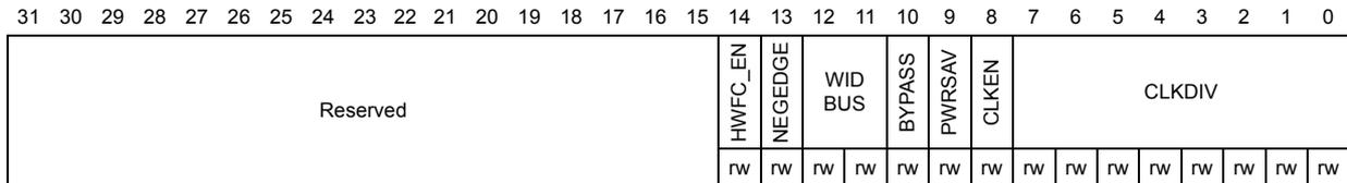
| 31 | 30 | 29 | 28 | 27 | 26 | 25 | 24 | 23 | 22 | 21 | 20 | 19 | 18 | 17 | 16 | 15 | 14 | 13 | 12 | 11 | 10 | 9 | 8 | 7 | 6 | 5 | 4 | 3 | 2 | 1 | 0 | |
| Reserved | HWFC_EN | NEGEDGE | WID BUS | BYPASS | PWRSV | CLKEN | CLKDIV | |||||||||||||||||||||||||
| rw | rw | rw | rw | rw | rw | rw | rw | rw | rw | rw | rw | rw | rw | rw | rw | rw | rw | |||||||||||||||
Bits 31:15 Reserved, must be kept at reset value
Bit 14 HWFC_EN : HW Flow Control enable
0b: HW Flow Control is disabled
1b: HW Flow Control is enabled
When HW Flow Control is enabled, the meaning of the TXFIFOE and RXFIFOE interrupt signals, see SDIO Status register definition in Section 21.9.11 .
Bit 13 NEGEDGE : SDIO_CK dephasing selection bit
0b: SDIO_CK generated on the rising edge of the master clock SDIOCLK
1b: SDIO_CK generated on the falling edge of the master clock SDIOCLK
Bits 12:11 WIDBUS : Wide bus mode enable bit
00: Default bus mode: SDIO_D0 used
01: 4-wide bus mode: SDIO_D[3:0] used
10: 8-wide bus mode: SDIO_D[7:0] used
Bit 10 BYPASS : Clock divider bypass enable bit
0: Disable bypass: SDIOCLK is divided according to the CLKDIV value before driving the SDIO_CK output signal.
1: Enable bypass: SDIOCLK directly drives the SDIO_CK output signal.
Bit 9 PWRSV : Power saving configuration bit
For power saving, the SDIO_CK clock output can be disabled when the bus is idle by setting PWRSV:
0: SDIO_CK clock is always enabled
1: SDIO_CK is only enabled when the bus is active
Bit 8 CLKEN : Clock enable bit
0: SDIO_CK is disabled
1: SDIO_CK is enabled
Bits 7:0 CLKDIV : Clock divide factor
This field defines the divide factor between the input clock (SDIOCLK) and the output clock (SDIO_CK): \( SDIO\_CK\ frequency = SDIOCLK / [CLKDIV + 2] \) .
Note: In order to have a duty cycle of 50% it is recommended to select even values of CLKDIV.
Note: While the SD/SDIO card or MultiMediaCard is in identification mode, the SDIO_CK frequency must be less than 400 kHz.
The clock frequency can be changed to the maximum card bus frequency when relative card addresses are assigned to all cards.
After a data write, data cannot be written to this register for three SDIOCLK clock periods plus two PCLK2 clock periods. SDIO_CK can also be stopped during the read wait interval for SD I/O cards: in this case the SDIO_CLKCR register does not control SDIO_CK.
21.9.3 SDIO argument register (SDIO_ARG)
Address offset: 0x08
Reset value: 0x0000 0000
The SDIO_ARG register contains a 32-bit command argument, which is sent to a card as part of a command message.

| 31 | 30 | 29 | 28 | 27 | 26 | 25 | 24 | 23 | 22 | 21 | 20 | 19 | 18 | 17 | 16 | 15 | 14 | 13 | 12 | 11 | 10 | 9 | 8 | 7 | 6 | 5 | 4 | 3 | 2 | 1 | 0 |
| CMDARG | |||||||||||||||||||||||||||||||
| rw | rw | rw | rw | rw | rw | rw | rw | rw | rw | rw | rw | rw | rw | rw | rw | rw | rw | rw | rw | rw | rw | rw | rw | rw | rw | rw | rw | rw | rw | rw | rw |
Bits 31:0 CMDARG : Command argument
Command argument sent to a card as part of a command message. If a command contains an argument, it must be loaded into this register before writing a command to the command register.
21.9.4 SDIO command register (SDIO_CMD)
Address offset: 0x0C
Reset value: 0x0000 0000
The SDIO_CMD register contains the command index and command type bits. The command index is sent to a card as part of a command message. The command type bits control the command path state machine (CPSM).
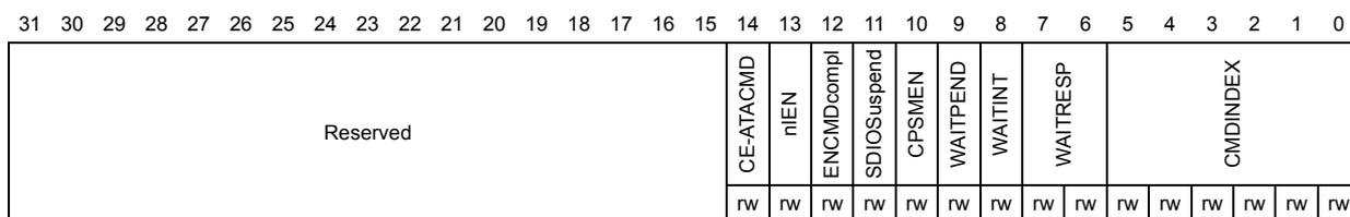
| 31 | 30 | 29 | 28 | 27 | 26 | 25 | 24 | 23 | 22 | 21 | 20 | 19 | 18 | 17 | 16 | 15 | 14 | 13 | 12 | 11 | 10 | 9 | 8 | 7 | 6 | 5 | 4 | 3 | 2 | 1 | 0 |
| Reserved | CE-ATACMD | nIEN | ENCMDcompl | SDIOSuspend | CPSMEN | WAITPEND | WAITINT | WAITRESP | CMDINDEX | ||||||||||||||||||||||
| rw | rw | rw | rw | rw | rw | rw | rw | rw | rw | rw | rw | rw | rw | rw | |||||||||||||||||
Bits 31:15 Reserved, must be kept at reset value
Bit 14 ATACMD : CE-ATA command
If ATACMD is set, the CPSM transfers CMD61.
Bit 13 nIEN : not Interrupt Enable
if this bit is 0, interrupts in the CE-ATA device are enabled.
Bit 12 ENCMDcompl : Enable CMD completion
If this bit is set, the command completion signal is enabled.
- Bit 11
SDIOSuspend
: SD I/O suspend command
If this bit is set, the command to be sent is a suspend command (to be used only with SDIO card). - Bit 10
CPSMEN
: Command path state machine (CPSM) Enable bit
If this bit is set, the CPSM is enabled. - Bit 9
WAITPEND
: CPSM Waits for ends of data transfer (CmdPend internal signal).
If this bit is set, the CPSM waits for the end of data transfer before it starts sending a command. - Bit 8
WAITINT
: CPSM waits for interrupt request
If this bit is set, the CPSM disables command timeout and waits for an interrupt request. - Bits 7:6
WAITRESP
: Wait for response bits
They are used to configure whether the CPSM is to wait for a response, and if yes, which kind of response.
00: No response, expect CMDSENT flag
01: Short response, expect CMDREND or CCRCFAIL flag
10: No response, expect CMDSENT flag
11: Long response, expect CMDREND or CCRCFAIL flag - Bits 5:0
CMDINDEX
: Command index
The command index is sent to the card as part of a command message.
Note: After a data write, data cannot be written to this register for three SDIOCLK clock periods plus two PCLK2 clock periods. MultiMediaCards can send two kinds of response: short responses, 48 bits long, or long responses, 136 bits long. SD card and SD I/O card can send only short responses, the argument can vary according to the type of response: the software distinguishes the type of response according to the sent command. CE-ATA devices send only short responses.
21.9.5 SDIO command response register (SDIO_RESPCMD)
Address offset: 0x10
Reset value: 0x0000 0000
The SDIO_RESPCMD register contains the command index field of the last command response received. If the command response transmission does not contain the command index field (long or OCR response), the RESPCMD field is unknown, although it must contain 111111b (the value of the reserved field from the response).

| 31 | 30 | 29 | 28 | 27 | 26 | 25 | 24 | 23 | 22 | 21 | 20 | 19 | 18 | 17 | 16 | 15 | 14 | 13 | 12 | 11 | 10 | 9 | 8 | 7 | 6 | 5 | 4 | 3 | 2 | 1 | 0 | |
| Reserved | RESPCMD | |||||||||||||||||||||||||||||||
| r | r | r | r | r | r | |||||||||||||||||||||||||||
Bits 31:6 Reserved, must be kept at reset value
Bits 5:0
RESPCMD
: Response command index
Read-only bit field. Contains the command index of the last command response received.
21.9.6 SDIO response 1..4 register (SDIO_RESPx)
Address offset: \( (0x10 + (4 \times x)) \) ; \( x = 1..4 \)
Reset value: 0x0000 0000
The SDIO_RESP1/2/3/4 registers contain the status of a card, which is part of the received response.

| 31 | 30 | 29 | 28 | 27 | 26 | 25 | 24 | 23 | 22 | 21 | 20 | 19 | 18 | 17 | 16 | 15 | 14 | 13 | 12 | 11 | 10 | 9 | 8 | 7 | 6 | 5 | 4 | 3 | 2 | 1 | 0 |
| CARDSTATUSx | |||||||||||||||||||||||||||||||
| r | r | r | r | r | r | r | r | r | r | r | r | r | r | r | r | r | r | r | r | r | r | r | r | r | r | r | r | r | r | r | r |
Bits 31:0 CARDSTATUSx : see Table 124 .
The Card Status size is 32 or 127 bits, depending on the response type.
Table 124. Response type and SDIO_RESPx registers
| Register | Short response | Long response |
|---|---|---|
| SDIO_RESP1 | Card Status[31:0] | Card Status [127:96] |
| SDIO_RESP2 | Unused | Card Status [95:64] |
| SDIO_RESP3 | Unused | Card Status [63:32] |
| SDIO_RESP4 | Unused | Card Status [31:1]0b |
The most significant bit of the card status is received first. The SDIO_RESP3 register LSB is always 0b.
21.9.7 SDIO data timer register (SDIO_DTIMER)
Address offset: 0x24
Reset value: 0x0000 0000
The SDIO_DTIMER register contains the data timeout period, in card bus clock periods.
A counter loads the value from the SDIO_DTIMER register, and starts decrementing when the data path state machine (DPSM) enters the Wait_R or Busy state. If the timer reaches 0 while the DPSM is in either of these states, the timeout status flag is set.

| 31 | 30 | 29 | 28 | 27 | 26 | 25 | 24 | 23 | 22 | 21 | 20 | 19 | 18 | 17 | 16 | 15 | 14 | 13 | 12 | 11 | 10 | 9 | 8 | 7 | 6 | 5 | 4 | 3 | 2 | 1 | 0 |
| DATATIME | |||||||||||||||||||||||||||||||
| rw | rw | rw | rw | rw | rw | rw | rw | rw | rw | rw | rw | rw | rw | rw | rw | rw | rw | rw | rw | rw | rw | rw | rw | rw | rw | rw | rw | rw | rw | rw | rw |
Bits 31:0 DATATIME : Data timeout period
Data timeout period expressed in card bus clock periods.
Note: A data transfer must be written to the data timer register and the data length register before being written to the data control register.
21.9.8 SDIO data length register (SDIO_DLEN)
Address offset: 0x28
Reset value: 0x0000 0000
The SDIO_DLEN register contains the number of data bytes to be transferred. The value is loaded into the data counter when data transfer starts.

| 31 | 30 | 29 | 28 | 27 | 26 | 25 | 24 | 23 | 22 | 21 | 20 | 19 | 18 | 17 | 16 | 15 | 14 | 13 | 12 | 11 | 10 | 9 | 8 | 7 | 6 | 5 | 4 | 3 | 2 | 1 | 0 |
| Reserved | DATALENGTH | ||||||||||||||||||||||||||||||
| rw | rw | rw | rw | rw | rw | rw | rw | rw | rw | rw | rw | rw | rw | rw | rw | rw | rw | rw | rw | rw | rw | rw | rw | rw | rw | rw | rw | rw | rw | rw | rw |
Bits 31:25 Reserved, must be kept at reset value
Bits 24:0
DATALENGTH
: Data length value
Number of data bytes to be transferred.
Note:
For a block data transfer, the value in the data length register must be a multiple of the block size (see SDIO_DCTRL). A data transfer must be written to the data timer register and the data length register before being written to the data control register.
For an SDIO multibyte transfer the value in the data length register must be between 1 and 512.
21.9.9 SDIO data control register (SDIO_DCTRL)
Address offset: 0x2C
Reset value: 0x0000 0000
The SDIO_DCTRL register control the data path state machine (DPSM).
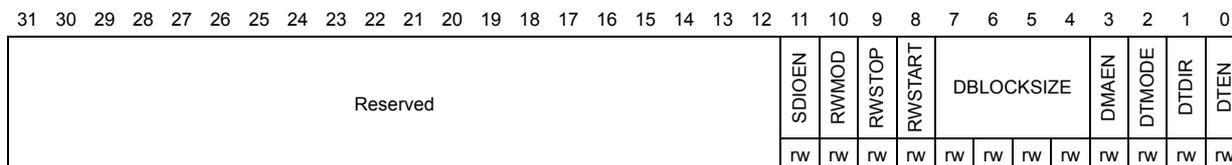
| 31 | 30 | 29 | 28 | 27 | 26 | 25 | 24 | 23 | 22 | 21 | 20 | 19 | 18 | 17 | 16 | 15 | 14 | 13 | 12 | 11 | 10 | 9 | 8 | 7 | 6 | 5 | 4 | 3 | 2 | 1 | 0 |
| Reserved | SDIOEN | RWMOD | RWSTOP | RWSTART | DBLOCKSIZE | DMAEN | DTMODE | DTDIR | DTEN | ||||||||||||||||||||||
| rw | rw | rw | rw | rw | rw | rw | rw | rw | |||||||||||||||||||||||
Bits 31:12 Reserved, must be kept at reset value
Bit 11 SDIOEN : SD I/O enable functions
If this bit is set, the DPSM performs an SD I/O-card-specific operation.
Bit 10 RWMOD : Read wait mode
- 0: Read Wait control stopping SDIO_D2
- 1: Read Wait control using SDIO_CK
Bit 9 RWSTOP : Read wait stop
- 0: Read wait in progress if RWSTART bit is set
- 1: Enable for read wait stop if RWSTART bit is set
Bit 8 RWSTART : Read wait start
If this bit is set, read wait operation starts.
Bits 7:4 DBLOCKSIZE : Data block size
Define the data block length when the block data transfer mode is selected:
- 0000: (0 decimal) block length = \( 2^0 \) = 1 byte
- 0001: (1 decimal) block length = \( 2^1 \) = 2 bytes
- 0010: (2 decimal) block length = \( 2^2 \) = 4 bytes
- 0011: (3 decimal) block length = \( 2^3 \) = 8 bytes
- 0100: (4 decimal) block length = \( 2^4 \) = 16 bytes
- 0101: (5 decimal) block length = \( 2^5 \) = 32 bytes
- 0110: (6 decimal) block length = \( 2^6 \) = 64 bytes
- 0111: (7 decimal) block length = \( 2^7 \) = 128 bytes
- 1000: (8 decimal) block length = \( 2^8 \) = 256 bytes
- 1001: (9 decimal) block length = \( 2^9 \) = 512 bytes
- 1010: (10 decimal) block length = \( 2^{10} \) = 1024 bytes
- 1011: (11 decimal) block length = \( 2^{11} \) = 2048 bytes
- 1100: (12 decimal) block length = \( 2^{12} \) = 4096 bytes
- 1101: (13 decimal) block length = \( 2^{13} \) = 8192 bytes
- 1110: (14 decimal) block length = \( 2^{14} \) = 16384 bytes
- 1111: (15 decimal) reserved
Bit 3 DMAEN : DMA enable bit
- 0: DMA disabled.
- 1: DMA enabled.
Bit 2 DTMODE : Data transfer mode selection 1: Stream or SDIO multibyte data transfer.
0: Block data transfer
1: Stream or SDIO multibyte data transfer
Bit 1 DTDIR : Data transfer direction selection
0: From controller to card.
1: From card to controller.
Bit 0 DTEN : Data transfer enabled bit
Data transfer starts if 1b is written to the DTEN bit. Depending on the direction bit, DTDIR, the DPSM moves to the Wait_S, Wait_R state or Readwait if RW Start is set immediately at the beginning of the transfer. It is not necessary to clear the enable bit after the end of a data transfer but the SDIO_DCTRL must be updated to enable a new data transfer
Note: After a data write, data cannot be written to this register for three SDIOCLK clock periods plus two PCLK2 clock periods.
The meaning of the DTMODE bit changes according to the value of the SDIOEN bit. When SDIOEN=0 and DTMODE=1, the MultiMediaCard stream mode is enabled, and when SDIOEN=1 and DTMODE=1, the peripheral enables an SDIO multibyte transfer.
21.9.10 SDIO data counter register (SDIO_DCOUNT)
Address offset: 0x30
Reset value: 0x0000 0000
The SDIO_DCOUNT register loads the value from the data length register (see SDIO_DLEN) when the DPSM moves from the Idle state to the Wait_R or Wait_S state. As data is transferred, the counter decrements the value until it reaches 0. The DPSM then moves to the Idle state and the data status end flag, DATAEND, is set.

| 31 | 30 | 29 | 28 | 27 | 26 | 25 | 24 | 23 | 22 | 21 | 20 | 19 | 18 | 17 | 16 | 15 | 14 | 13 | 12 | 11 | 10 | 9 | 8 | 7 | 6 | 5 | 4 | 3 | 2 | 1 | 0 |
| Reserved | DATACOUNT | ||||||||||||||||||||||||||||||
| r | r | r | r | r | r | r | r | r | r | r | r | r | r | r | r | r | r | r | r | r | r | r | r | r | |||||||
Bits 31:25 Reserved, must be kept at reset value
Bits 24:0 DATACOUNT : Data count value
When this bit is read, the number of remaining data bytes to be transferred is returned. Write has no effect.
Note: This register should be read only when the data transfer is complete.
21.9.11 SDIO status register (SDIO_STA)
Address offset: 0x34
Reset value: 0x0000 0000
The SDIO_STA register is a read-only register. It contains two types of flag:
- • Static flags (bits [23:22,10:0]): these bits remain asserted until they are cleared by writing to the SDIO Interrupt Clear register (see SDIO_ICR)
- • Dynamic flags (bits [21:11]): these bits change state depending on the state of the underlying logic (for example, FIFO full and empty flags are asserted and deasserted as data while written to the FIFO)
| 31 | 30 | 29 | 28 | 27 | 26 | 25 | 24 | 23 | 22 | 21 | 20 | 19 | 18 | 17 | 16 | 15 | 14 | 13 | 12 | 11 | 10 | 9 | 8 | 7 | 6 | 5 | 4 | 3 | 2 | 1 | 0 |
|---|---|---|---|---|---|---|---|---|---|---|---|---|---|---|---|---|---|---|---|---|---|---|---|---|---|---|---|---|---|---|---|
| Reserved | CEATAEND | SDIOIT | RXDAVL | TXDAVL | RXFIFOE | TXFIFOE | RXFIFOF | TXFIFOF | RXFIFOHF | TXFIFOHE | RXACT | TXACT | CMDACT | DBCKEND | STBITERR | DATAEND | CMDSENT | CMDREND | RXOVERR | TXUNDER | DTIMEOUT | CTIMEOUT | DCRCFAIL | CCRCFAIL | |||||||
| r | r | r | r | r | r | r | r | r | r | r | r | r | r | r | r | r | r | r | r | r | r | r | r | r | r | r | r | r | r | r | r |
Bits 31:24 Reserved, must be kept at reset value
Bit 23 CEATAEND : CE-ATA command completion signal received for CMD61
Bit 22 SDIOIT : SDIO interrupt received
Bit 21 RXDAVL : Data available in receive FIFO
Bit 20 TXDAVL : Data available in transmit FIFO
Bit 19 RXFIFOE : Receive FIFO empty
Bit 18 TXFIFOE : Transmit FIFO empty
When HW Flow Control is enabled, TXFIFOE signals becomes activated when the FIFO contains 2 words.
Bit 17 RXFIFOF : Receive FIFO full
When HW Flow Control is enabled, RXFIFOF signals becomes activated 2 words before the FIFO is full.
Bit 16 TXFIFOF : Transmit FIFO full
Bit 15 RXFIFOHF : Receive FIFO half full: there are at least 8 words in the FIFO
Bit 14 TXFIFOHE : Transmit FIFO half empty: at least 8 words can be written into the FIFO
Bit 13 RXACT : Data receive in progress
Bit 12 TXACT : Data transmit in progress
Bit 11 CMDACT : Command transfer in progress
Bit 10 DBCKEND : Data block sent/received (CRC check passed)
Bit 9 STBITERR : Start bit not detected on all data signals in wide bus mode
Bit 8 DATAEND : Data end (data counter, SDIDCOUNT, is zero)
Bit 7 CMDSENT : Command sent (no response required)
Bit 6 CMDREND : Command response received (CRC check passed)
Bit 5 RXOVERR : Received FIFO overrun error
Bit 4 TXUNDERR : Transmit FIFO underrun error
Bit 3 DTIMEOUT : Data timeout
Bit 2 CTIMEOUT : Command response timeout
The Command TimeOut period has a fixed value of 64 SDIO_CK clock periods.
Bit 1 DCRCFAIL : Data block sent/received (CRC check failed)
Bit 0 CCRCFAIL : Command response received (CRC check failed)
21.9.12 SDIO interrupt clear register (SDIO_ICR)
Address offset: 0x38
Reset value: 0x0000 0000
The SDIO_ICR register is a write-only register. Writing a bit with 1b clears the corresponding bit in the SDIO_STA Status register.
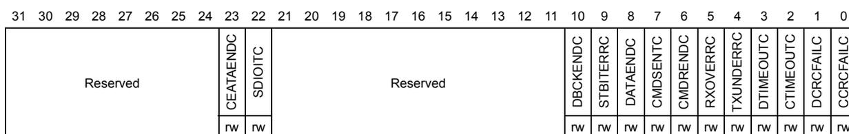
| 31 | 30 | 29 | 28 | 27 | 26 | 25 | 24 | 23 | 22 | 21 | 20 | 19 | 18 | 17 | 16 | 15 | 14 | 13 | 12 | 11 | 10 | 9 | 8 | 7 | 6 | 5 | 4 | 3 | 2 | 1 | 0 |
|---|---|---|---|---|---|---|---|---|---|---|---|---|---|---|---|---|---|---|---|---|---|---|---|---|---|---|---|---|---|---|---|
| Reserved | CEATAENDC | SDIOITC | Reserved | DBCKENDC | STBITERRC | DATAENDC | CMDSENTC | CMDREND | RXOVERERRC | TXUNDERRC | DTIMEOUTC | CTIMEOUTC | DCRCFAILC | CCRCFAILC | |||||||||||||||||
| rw | rw | rw | rw | rw | rw | rw | rw | rw | rw | rw | rw | rw | rw | ||||||||||||||||||
Bits 31:24 Reserved, must be kept at reset value
Bit 23 CEATAENDC : CEATAEND flag clear bit
Set by software to clear the CEATAEND flag.
0: CEATAEND not cleared
1: CEATAEND cleared
Bit 22 SDIOITC : SDIOIT flag clear bit
Set by software to clear the SDIOIT flag.
0: SDIOIT not cleared
1: SDIOIT cleared
Bits 21:11 Reserved, must be kept at reset value
Bit 10 DBCKENDC : DBCKEND flag clear bit
Set by software to clear the DBCKEND flag.
0: DBCKEND not cleared
1: DBCKEND cleared
Bit 9 STBITERRC : STBITERR flag clear bit
Set by software to clear the STBITERR flag.
0: STBITERR not cleared
1: STBITERR cleared
Bit 8 DATAENDC : DATAEND flag clear bit
Set by software to clear the DATAEND flag.
0: DATAEND not cleared
1: DATAEND cleared
- Bit 7
CMDSENTC
: CMDSENT flag clear bit
Set by software to clear the CMDSENT flag.
0: CMDSENT not cleared
1: CMDSENT cleared - Bit 6
CMDREND
: CMDREND flag clear bit
Set by software to clear the CMDREND flag.
0: CMDREND not cleared
1: CMDREND cleared - Bit 5
RXOVERRC
: RXOVER flag clear bit
Set by software to clear the RXOVER flag.
0: RXOVER not cleared
1: RXOVER cleared - Bit 4
TXUNDERRC
: TXUNDERR flag clear bit
Set by software to clear the TXUNDERR flag.
0: TXUNDERR not cleared
1: TXUNDERR cleared - Bit 3
DTIMEOUTC
: DTIMEOUT flag clear bit
Set by software to clear the DTIMEOUT flag.
0: DTIMEOUT not cleared
1: DTIMEOUT cleared - Bit 2
CTIMEOUTC
: CTIMEOUT flag clear bit
Set by software to clear the CTIMEOUT flag.
0: CTIMEOUT not cleared
1: CTIMEOUT cleared - Bit 1
DCRCFAILC
: DCRCFAIL flag clear bit
Set by software to clear the DCRCFAIL flag.
0: DCRCFAIL not cleared
1: DCRCFAIL cleared - Bit 0
CCRCFAILC
: CCRCFAIL flag clear bit
Set by software to clear the CCRCFAIL flag.
0: CCRCFAIL not cleared
1: CCRCFAIL cleared
21.9.13 SDIO mask register (SDIO_MASK)
Address offset: 0x3C
Reset value: 0x0000 0000
The interrupt mask register determines which status flags generate an interrupt request by setting the corresponding bit to 1b.
| 31 | 30 | 29 | 28 | 27 | 26 | 25 | 24 | 23 | 22 | 21 | 20 | 19 | 18 | 17 | 16 | 15 | 14 | 13 | 12 | 11 | 10 | 9 | 8 | 7 | 6 | 5 | 4 | 3 | 2 | 1 | 0 |
|---|---|---|---|---|---|---|---|---|---|---|---|---|---|---|---|---|---|---|---|---|---|---|---|---|---|---|---|---|---|---|---|
| Reserved | |||||||||||||||||||||||||||||||
| CEATAENDIE | SDIOITIE | RXDAVLIE | TXDAVLIE | RXFIFOEIE | TXFIFOEIE | RXFIFOIE | TXFIFOIE | RXFIFOHIE | TXFIFOHIE | RXACTIE | TXACTIE | CMDACTIE | DBCKENDIE | STBITERRIE | DATAENDIE | CMDSENTIE | CMDRENDIE | RXOVERRIE | TXUNDERIE | DTIMEOUTIE | CTIMEOUTIE | DORCFALLIE | CCRCFALLIE | ||||||||
| rw | rw | rw | rw | rw | rw | rw | rw | rw | rw | rw | rw | rw | rw | rw | rw | rw | rw | rw | rw | rw | rw | rw | rw | ||||||||
Bits 31:24 Reserved, must be kept at reset value
Bit 23 CEATAENDIE : CE-ATA command completion signal received interrupt enable
Set and cleared by software to enable/disable the interrupt generated when receiving the CE-ATA command completion signal.
0: CE-ATA command completion signal received interrupt disabled
1: CE-ATA command completion signal received interrupt enabled
Bit 22 SDIOITIE : SDIO mode interrupt received interrupt enable
Set and cleared by software to enable/disable the interrupt generated when receiving the SDIO mode interrupt.
0: SDIO Mode Interrupt Received interrupt disabled
1: SDIO Mode Interrupt Received interrupt enabled
Bit 21 RXDAVLIE : Data available in Rx FIFO interrupt enable
Set and cleared by software to enable/disable the interrupt generated by the presence of data available in Rx FIFO.
0: Data available in Rx FIFO interrupt disabled
1: Data available in Rx FIFO interrupt enabled
Bit 20 TXDAVLIE : Data available in Tx FIFO interrupt enable
Set and cleared by software to enable/disable the interrupt generated by the presence of data available in Tx FIFO.
0: Data available in Tx FIFO interrupt disabled
1: Data available in Tx FIFO interrupt enabled
Bit 19 RXFIFOEIE : Rx FIFO empty interrupt enable
Set and cleared by software to enable/disable interrupt caused by Rx FIFO empty.
0: Rx FIFO empty interrupt disabled
1: Rx FIFO empty interrupt enabled
Bit 18 TXFIFOEIE : Tx FIFO empty interrupt enable
Set and cleared by software to enable/disable interrupt caused by Tx FIFO empty.
0: Tx FIFO empty interrupt disabled
1: Tx FIFO empty interrupt enabled
Bit 17 RXFIFOIE : Rx FIFO full interrupt enable
Set and cleared by software to enable/disable interrupt caused by Rx FIFO full.
0: Rx FIFO full interrupt disabled
1: Rx FIFO full interrupt enabled
Bit 16 TXFIFOIE : Tx FIFO full interrupt enable
Set and cleared by software to enable/disable interrupt caused by Tx FIFO full.
0: Tx FIFO full interrupt disabled
1: Tx FIFO full interrupt enabled
Bit 15 RXFIFOIE : Rx FIFO half full interrupt enable
Set and cleared by software to enable/disable interrupt caused by Rx FIFO half full.
0: Rx FIFO half full interrupt disabled
1: Rx FIFO half full interrupt enabled
Bit 14 TXFIFOIE : Tx FIFO half empty interrupt enable
Set and cleared by software to enable/disable interrupt caused by Tx FIFO half empty.
0: Tx FIFO half empty interrupt disabled
1: Tx FIFO half empty interrupt enabled
Bit 13 RXACTIE : Data receive acting interrupt enable
Set and cleared by software to enable/disable interrupt caused by data being received (data receive acting).
0: Data receive acting interrupt disabled
1: Data receive acting interrupt enabled
Bit 12 TXACTIE : Data transmit acting interrupt enable
Set and cleared by software to enable/disable interrupt caused by data being transferred (data transmit acting).
0: Data transmit acting interrupt disabled
1: Data transmit acting interrupt enabled
Bit 11 CMRACTIE : Command acting interrupt enable
Set and cleared by software to enable/disable interrupt caused by a command being transferred (command acting).
0: Command acting interrupt disabled
1: Command acting interrupt enabled
Bit 10 DBCKENDIE : Data block end interrupt enable
Set and cleared by software to enable/disable interrupt caused by data block end.
0: Data block end interrupt disabled
1: Data block end interrupt enabled
Bit 9 STBITERRIE : Start bit error interrupt enable
Set and cleared by software to enable/disable interrupt caused by start bit error.
0: Start bit error interrupt disabled
1: Start bit error interrupt enabled
Bit 8 DATAENDIE : Data end interrupt enable
Set and cleared by software to enable/disable interrupt caused by data end.
0: Data end interrupt disabled
1: Data end interrupt enabled
Bit 7 CMDSENTIE : Command sent interrupt enable
Set and cleared by software to enable/disable interrupt caused by sending command.
0: Command sent interrupt disabled
1: Command sent interrupt enabled
Bit 6 CMDRENDIE : Command response received interrupt enable
Set and cleared by software to enable/disable interrupt caused by receiving command response.
0: Command response received interrupt disabled
1: command Response Received interrupt enabledBit 5 RXOVERRIE : Rx FIFO overrun error interrupt enable
Set and cleared by software to enable/disable interrupt caused by Rx FIFO overrun error.
0: Rx FIFO overrun error interrupt disabled
1: Rx FIFO overrun error interrupt enabledBit 4 TXUNDERRIE : Tx FIFO underrun error interrupt enable
Set and cleared by software to enable/disable interrupt caused by Tx FIFO underrun error.
0: Tx FIFO underrun error interrupt disabled
1: Tx FIFO underrun error interrupt enabledBit 3 DTIMEOUTIE : Data timeout interrupt enable
Set and cleared by software to enable/disable interrupt caused by data timeout.
0: Data timeout interrupt disabled
1: Data timeout interrupt enabledBit 2 CTIMEOUTIE : Command timeout interrupt enable
Set and cleared by software to enable/disable interrupt caused by command timeout.
0: Command timeout interrupt disabled
1: Command timeout interrupt enabledBit 1 DCRCFAILIE : Data CRC fail interrupt enable
Set and cleared by software to enable/disable interrupt caused by data CRC failure.
0: Data CRC fail interrupt disabled
1: Data CRC fail interrupt enabledBit 0 CCRCFAILIE : Command CRC fail interrupt enable
Set and cleared by software to enable/disable interrupt caused by command CRC failure.
0: Command CRC fail interrupt disabled
1: Command CRC fail interrupt enabled
21.9.14 SDIO FIFO counter register (SDIO_FIFOCNT)
Address offset: 0x48
Reset value: 0x0000 0000
The SDIO_FIFOCNT register contains the remaining number of words to be written to or read from the FIFO. The FIFO counter loads the value from the data length register (see SDIO_DLEN) when the data transfer enable bit, DTEN, is set in the data control register (SDIO_DCTRL register) and the DPSM is at the Idle state. If the data length is not word-aligned (multiple of 4), the remaining 1 to 3 bytes are regarded as a word.
| 31 | 30 | 29 | 28 | 27 | 26 | 25 | 24 | 23 | 22 | 21 | 20 | 19 | 18 | 17 | 16 | 15 | 14 | 13 | 12 | 11 | 10 | 9 | 8 | 7 | 6 | 5 | 4 | 3 | 2 | 1 | 0 |
|---|---|---|---|---|---|---|---|---|---|---|---|---|---|---|---|---|---|---|---|---|---|---|---|---|---|---|---|---|---|---|---|
| Reserved | FIFOCOUNT | ||||||||||||||||||||||||||||||
| r | r | r | r | r | r | r | r | r | r | r | r | r | r | r | r | r | r | r | r | r | r | r | r | r | r | r | r | r | r | r | r |
Bits 31:24 Reserved, must be kept at reset value
Bits 23:0 FIFOCOUNT : Remaining number of words to be written to or read from the FIFO.
21.9.15 SDIO data FIFO register (SDIO_FIFO)
Address offset: 0x80
Reset value: 0x0000 0000
The receive and transmit FIFOs can be read or written as 32-bit wide registers. The FIFOs contain 32 entries on 32 sequential addresses. This allows the CPU to use its load and store multiple operands to read from/write to the FIFO.

| 31 | 30 | 29 | 28 | 27 | 26 | 25 | 24 | 23 | 22 | 21 | 20 | 19 | 18 | 17 | 16 | 15 | 14 | 13 | 12 | 11 | 10 | 9 | 8 | 7 | 6 | 5 | 4 | 3 | 2 | 1 | 0 |
| FIFOData | |||||||||||||||||||||||||||||||
| rw | rw | rw | rw | rw | rw | rw | rw | rw | rw | rw | rw | rw | rw | rw | rw | rw | rw | rw | rw | rw | rw | rw | rw | rw | rw | rw | rw | rw | rw | rw | rw |
bits 31:0 FIFOData : Receive and transmit FIFO data
The FIFO data occupies 32 entries of 32-bit words, from address:
SDIO base + 0x080 to SDIO base + 0xFC.
21.9.16 SDIO register map
The following table summarizes the SDIO registers.
Table 125. SDIO register map
| Offset | Register | 31 | 30 | 29 | 28 | 27 | 26 | 25 | 24 | 23 | 22 | 21 | 20 | 19 | 18 | 17 | 16 | 15 | 14 | 13 | 12 | 11 | 10 | 9 | 8 | 7 | 6 | 5 | 4 | 3 | 2 | 1 | 0 |
|---|---|---|---|---|---|---|---|---|---|---|---|---|---|---|---|---|---|---|---|---|---|---|---|---|---|---|---|---|---|---|---|---|---|
| 0x00 | SDIO_POWER | Reserved | PWRCTRL | ||||||||||||||||||||||||||||||
| 0x04 | SDIO_CLKCR | Reserved | HWFC_EN | NEGEDGE | WIDBUS | BYPASS | PWRSV | CLKEN | CLKDIV | ||||||||||||||||||||||||
| 0x08 | SDIO_ARG | CMDARG | |||||||||||||||||||||||||||||||
| 0x0C | SDIO_CMD | Reserved | CE-ATACMD | nIEN | ENCMDcompl | SDIOSuspend | CPSMEN | WAITPEND | WAITINT | WAITRESP | CMDINDEX | ||||||||||||||||||||||
| 0x10 | SDIO_RESPCMD | Reserved | RESPCMD | ||||||||||||||||||||||||||||||
| 0x14 | SDIO_RESP1 | CARDSTATUS1 | |||||||||||||||||||||||||||||||
| 0x18 | SDIO_RESP2 | CARDSTATUS2 | |||||||||||||||||||||||||||||||
| 0x1C | SDIO_RESP3 | CARDSTATUS3 | |||||||||||||||||||||||||||||||
| 0x20 | SDIO_RESP4 | CARDSTATUS4 | |||||||||||||||||||||||||||||||
| 0x24 | SDIO_DTIMER | DATATIME | |||||||||||||||||||||||||||||||
| 0x28 | SDIO_DLEN | Reserved | DATALENGTH | ||||||||||||||||||||||||||||||
| 0x2C | SDIO_DCTRL | Reserved | SDIOEN | RWMOD | RWSTOP | RWSTART | DBLOCKSIZE | DMAEN | DTMODE | DTDIR | DTEN | ||||||||||||||||||||||
| 0x30 | SDIO_DCOUNT | Reserved | DATACOUNT | ||||||||||||||||||||||||||||||
Table 125. SDIO register map (continued)
| Offset | Register | 31 | 30 | 29 | 28 | 27 | 26 | 25 | 24 | 23 | 22 | 21 | 20 | 19 | 18 | 17 | 16 | 15 | 14 | 13 | 12 | 11 | 10 | 9 | 8 | 7 | 6 | 5 | 4 | 3 | 2 | 1 | 0 |
|---|---|---|---|---|---|---|---|---|---|---|---|---|---|---|---|---|---|---|---|---|---|---|---|---|---|---|---|---|---|---|---|---|---|
| 0x34 | SDIO_STA | Reserved | CEATAEND | SDIOIT | RXDAVL | TXDAVL | RXFIFOE | TXFIFOE | RXFIFO | TXFIFO | RXFIFOHF | TXFIFOHE | RXACT | TXACT | CMDACT | DBCKEND | STBITERR | DATAEND | CMDSENT | CMDREND | RXOVER | TXUNDER | DTIMEOUT | CTIMEOUT | DCRCFAIL | CCRCFAIL | |||||||
| 0x38 | SDIO_ICR | Reserved | CEATAENDC | SDIOITC | Reserved | DBCKENDC | STBITERRC | DATAENDC | CMDSENTC | CMDREND | RXOVER | TXUNDER | DTIMEOUT | CTIMEOUT | DCRCFAIL | CCRCFAIL | |||||||||||||||||
| 0x3C | SDIO_MASK | Reserved | CEATAENDIE | SDIOITIE | RXDAVLIE | TXDAVLIE | RXFIFOEIE | TXFIFOEIE | RXFIFOIE | TXFIFOIE | RXFIFOHFIE | TXFIFOHEIE | RXACTIE | TXACTIE | CMDACTIE | DBCKENDIE | STBITERRIE | DATAENDIE | CMDSENTIE | CMDRENDIE | RXOVERIE | TXUNDERIE | DTIMEOUTIE | CTIMEOUTIE | DCRCFAILIE | CCRCFAILIE | |||||||
| 0x48 | SDIO_FIFOCNT | Reserved | FIFOCOUNT | ||||||||||||||||||||||||||||||
| 0x80 | SDIO_FIFO | FIF0Data | |||||||||||||||||||||||||||||||