16. Window watchdog (WWDG)
16.1 WWDG introduction
The window watchdog is used to detect the occurrence of a software fault, usually generated by external interference or by unforeseen logical conditions, which causes the application program to abandon its normal sequence. The watchdog circuit generates an MCU reset on expiry of a programmed time period, unless the program refreshes the contents of the downcounter before the T6 bit becomes cleared. An MCU reset is also generated if the 7-bit downcounter value (in the control register) is refreshed before the downcounter has reached the window register value. This implies that the counter must be refreshed in a limited window.
16.2 WWDG main features
- • Programmable free-running downcounter
- • Conditional reset
- – Reset (if watchdog activated) when the downcounter value becomes less than 0x40
- – Reset (if watchdog activated) if the downcounter is reloaded outside the window (see Figure 158 )
- • Early wake-up interrupt (EWI): triggered (if enabled and the watchdog activated) when the downcounter is equal to 0x40.
16.3 WWDG functional description
If the watchdog is activated (the WDGA bit is set in the WWDG_CR register) and when the 7-bit downcounter (T[6:0] bits) rolls over from 0x40 to 0x3F (T6 becomes cleared), it initiates a reset. If the software reloads the counter while the counter is greater than the value stored in the window register, then a reset is generated.
Figure 157. Watchdog block diagram
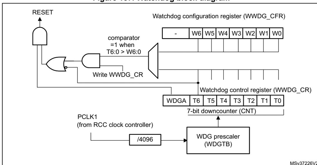
The diagram illustrates the internal architecture of the Window Watchdog (WWDG). At the bottom, a 'WDG prescaler (WDGTB)' block receives 'PCLK1 (from RCC clock controller)' and divides it by 4096. The output of the prescaler feeds into a '7-bit downcounter (CNT)'. The downcounter has eight output bits: WDGA, T6, T5, T4, T3, T2, T1, and T0, which are shown in the 'Watchdog control register (WWDG_CR)'. Above the downcounter is a 'comparator' block. It compares the counter's current value (T6:0) with the values stored in the 'Watchdog configuration register (WWDG_CFR)', which are W6, W5, W4, W3, W2, W1, and W0. The comparator output is labeled 'comparator = 1 when T6:0 > W6:0'. This output is connected to one input of an AND gate. The other input of the AND gate is labeled 'Write WWDG_CR'. The output of the AND gate is connected to one input of an OR gate. The other input of the OR gate is labeled 'RESET'. The output of the OR gate is the final 'RESET' signal.
The application program must write in the WWDG_CR register at regular intervals during normal operation to prevent an MCU reset. This operation must occur only when the counter value is lower than the window register value. The value to be stored in the WWDG_CR register must be between 0xFF and 0xC0.
Enabling the watchdog
The watchdog is always disabled after a reset. It is enabled by setting the WDGA bit in the WWDG_CR register, then it cannot be disabled again except by a reset.
Controlling the downcounter
This downcounter is free-running, counting down even if the watchdog is disabled. When the watchdog is enabled, the T6 bit must be set to prevent generating an immediate reset.
The T[5:0] bits contain the number of increments which represents the time delay before the watchdog produces a reset. The timing varies between a minimum and a maximum value due to the unknown status of the prescaler when writing to the WWDG_CR register (see Figure 158 ). The Configuration register (WWDG_CFR) contains the high limit of the window: To prevent a reset, the downcounter must be reloaded when its value is lower than the window register value and greater than 0x3F. Figure 158 describes the window watchdog process.
Note: The T6 bit can be used to generate a software reset (the WDGA bit is set and the T6 bit is cleared).
Advanced watchdog interrupt feature
The Early Wake-up Interrupt (EWI) can be used if specific safety operations or data logging must be performed before the actual reset is generated. The EWI interrupt is enabled by setting the EWI bit in the WWDG_CFR register. When the downcounter reaches the value 0x40, an EWI interrupt is generated and the corresponding interrupt service routine (ISR) can be used to trigger specific actions (such as communications or data logging), before resetting the device.
In some applications, the EWI interrupt can be used to manage a software system check and/or system recovery/graceful degradation, without generating a WWDG reset. In this case, the corresponding interrupt service routine (ISR) should reload the WWDG counter to avoid the WWDG reset, then trigger the required actions.
The EWI interrupt is cleared by writing '0' to the EWIF bit in the WWDG_SR register.
Note: When the EWI interrupt cannot be served (due to a system lock in a higher priority task), the WWDG reset is eventually generated.
16.4 How to program the watchdog timeout
Warning: When writing to the WWDG_CR register, always write 1 in the T6 bit to avoid generating an immediate reset.
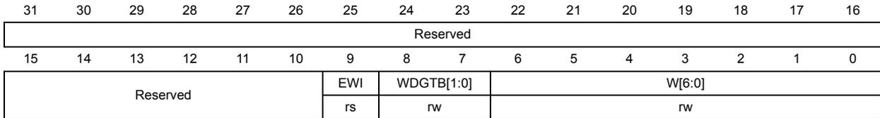
Figure 158. Window watchdog timing diagram
![Figure 158. Window watchdog timing diagram. The diagram shows three waveforms over time. The top waveform is the T[6:0] CNT downcounter, which starts at a value W[6:0] and decreases linearly to 0x3F. The middle waveform is the T6 bit, which is high during the 'Refresh not allowed' period and goes low when the counter reaches 0x3F. The bottom waveform is the RESET signal, which pulses low when the counter reaches 0x3F. The time interval from the start until the counter reaches 0x3F is labeled 'Refresh not allowed', and the subsequent time interval is labeled 'Refresh allowed'. The diagram is labeled ai17101c.](/RM0368-STM32F401xB-C-401xD-E/2a046f70c6b6840a8e80920e7e46db92_img.jpg)
The formula to calculate the WWDG timeout value is given by:
where:
\( t_{\text{WWDG}} \) : WWDG timeout
\( t_{\text{PCLK1}} \) : APB1 clock period measured in ms
4096: value corresponding to internal divider
As an example, let us assume APB1 frequency is equal to 24 MHz, WDGTB[1:0] is set to 3 and T[5:0] is set to 63:
Refer to Table 64 for the minimum and maximum values of the \( t_{\text{WWDG}} \) .
Table 64. Minimum and maximum timeout values at 30 MHz ( \( f_{\text{PCLK1}} \) )
| Prescaler | WDGTB | Min timeout (
\(
\mu\text{s}
\)
) T[5:0] = 0x00 | Max timeout (ms) T[5:0] = 0x3F |
|---|---|---|---|
| 1 | 0 | 136.53 | 8.74 |
| 2 | 1 | 273.07 | 17.48 |
| 4 | 2 | 546.13 | 34.95 |
| 8 | 3 | 1092.27 | 69.91 |
16.5 Debug mode
When the microcontroller enters debug mode (Cortex ® -M4 with FPU core halted), the WWDG counter either continues to work normally or stops, depending on DBG_WWDG_STOP configuration bit in DBG module. For more details, refer to Section 23.16.2: Debug support for timers, watchdog and I 2 C .
16.6 WWDG registers
Refer to Section 2.2 on page 45 for a list of abbreviations used in register descriptions.
The peripheral registers have to be accessed by half-words (16 bits) or words (32 bits).
16.6.1 Control register (WWDG_CR)
Address offset: 0x00
Reset value: 0x0000 007F
| 31 | 30 | 29 | 28 | 27 | 26 | 25 | 24 | 23 | 22 | 21 | 20 | 19 | 18 | 17 | 16 |
|---|---|---|---|---|---|---|---|---|---|---|---|---|---|---|---|
| Reserved | |||||||||||||||
| 15 | 14 | 13 | 12 | 11 | 10 | 9 | 8 | 7 | 6 | 5 | 4 | 3 | 2 | 1 | 0 |
| Reserved | WDGA | T[6:0] | |||||||||||||
| rs | rw | ||||||||||||||
Bits 31:8 Reserved, must be kept at reset value.
Bit 7 WDGA : Activation bit
This bit is set by software and only cleared by hardware after a reset. When WDGA = 1, the watchdog can generate a reset.
0: Watchdog disabled
1: Watchdog enabled
Bits 6:0 T[6:0] : 7-bit counter (MSB to LSB)
These bits contain the value of the watchdog counter. It is decremented every \( (4096 \times 2^{\text{WDGTB}[1:0]}) \) PCLK1 cycles. A reset is produced when it rolls over from 0x40 to 0x3F (T6 becomes cleared).
16.6.2 Configuration register (WWDG_CFR)
Address offset: 0x04
Reset value: 0x0000 007F
| 31 | 30 | 29 | 28 | 27 | 26 | 25 | 24 | 23 | 22 | 21 | 20 | 19 | 18 | 17 | 16 |
| Reserved | |||||||||||||||
| 15 | 14 | 13 | 12 | 11 | 10 | 9 | 8 | 7 | 6 | 5 | 4 | 3 | 2 | 1 | 0 |
| Reserved | EWI | WDGTB[1:0] | W[6:0] | ||||||||||||
| rs | rw | rw | |||||||||||||
Bit 31:10 Reserved, must be kept at reset value.
Bit 9 EWI : Early wake-up interrupt
When set, an interrupt occurs whenever the counter reaches the value 0x40. This interrupt is only cleared by hardware after a reset.
Bits 8:7 WDGTB[1:0] : Timer base
The time base of the prescaler can be modified as follows:
- 00: CK Counter Clock (PCLK1 div 4096) div 1
- 01: CK Counter Clock (PCLK1 div 4096) div 2
- 10: CK Counter Clock (PCLK1 div 4096) div 4
- 11: CK Counter Clock (PCLK1 div 4096) div 8
Bits 6:0 W[6:0] : 7-bit window value
These bits contain the window value to be compared to the downcounter.
16.6.3 Status register (WWDG_SR)
Address offset: 0x08
Reset value: 0x0000 0000
| 31 | 30 | 29 | 28 | 27 | 26 | 25 | 24 | 23 | 22 | 21 | 20 | 19 | 18 | 17 | 16 |
| Reserved | |||||||||||||||
| 15 | 14 | 13 | 12 | 11 | 10 | 9 | 8 | 7 | 6 | 5 | 4 | 3 | 2 | 1 | 0 |
| Reserved | EWIF | ||||||||||||||
| rc_w0 | |||||||||||||||
Bits 31:1 Reserved, must be kept at reset value.
Bit 0 EWIF : Early wake-up interrupt flag
This bit is set by hardware when the counter has reached the value 0x40. It must be cleared by software by writing ‘0’. A write of ‘1’ has no effect. This bit is also set if the interrupt is not enabled.
16.6.4 WWDG register map
The following table gives the WWDG register map and reset values.
Table 65. WWDG register map and reset values
| Offset | Register | 31 | 30 | 29 | 28 | 27 | 26 | 25 | 24 | 23 | 22 | 21 | 20 | 19 | 18 | 17 | 16 | 15 | 14 | 13 | 12 | 11 | 10 | 9 | 8 | 7 | 6 | 5 | 4 | 3 | 2 | 1 | 0 | ||
|---|---|---|---|---|---|---|---|---|---|---|---|---|---|---|---|---|---|---|---|---|---|---|---|---|---|---|---|---|---|---|---|---|---|---|---|
| 0x00 | WWDG_CR | Reserved | WDGA | T[6:0] | |||||||||||||||||||||||||||||||
| Reset value | 0 | 1 | 1 | 1 | 1 | 1 | 1 | 1 | 1 | ||||||||||||||||||||||||||
| 0x04 | WWDG_CFR | Reserved | EWI | WDGTB1 | W[6:0] | ||||||||||||||||||||||||||||||
| Reset value | 0 | 0 | |||||||||||||||||||||||||||||||||
| 0x08 | WWDG_SR | Reserved | EWIF | ||||||||||||||||||||||||||||||||
| Reset value | 0 | ||||||||||||||||||||||||||||||||||
Refer to Section 3.3: Memory map for the register boundary addresses.