10. Interrupts and events
10.1 Nested vectored interrupt controller (NVIC)
10.1.1 NVIC features
The nested vector interrupt controller NVIC includes the following features:
- • 52 maskable interrupt channels (not including the 16 interrupt lines of Cortex ® -M4 with FPU)
- • 16 programmable priority levels (4 bits of interrupt priority are used)
- • low-latency exception and interrupt handling
- • power management control
- • implementation of system control registers
The NVIC and the processor core interface are closely coupled, which enables low latency interrupt processing and efficient processing of late arriving interrupts.
All interrupts including the core exceptions are managed by the NVIC. For more information on exceptions and NVIC programming, refer to programming manual PM0214.
10.1.2 SysTick calibration value register
The SysTick calibration value is fixed to 10500, which gives a reference time base of 1 ms with the SysTick clock set to 10.5 MHz (HCLK/8, with HCLK set to 84 MHz).
10.1.3 Interrupt and exception vectors
See Table 38 , for the vector table for the STM32F401xB/C and STM32F401xD/E devices.
10.2 External interrupt/event controller (EXTI)
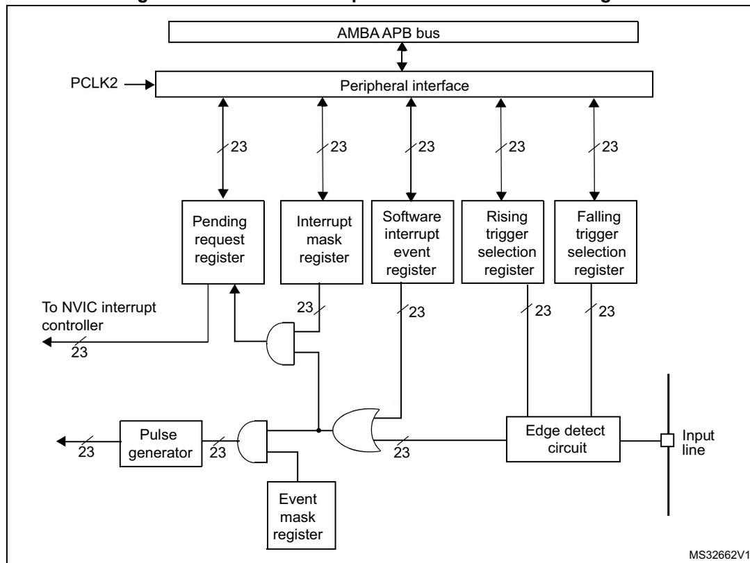
The external interrupt/event controller consists of up to 23 edge detectors for generating event/interrupt requests. Each input line can be independently configured to select the type (interrupt or event) and the corresponding trigger event (rising or falling or both). Each line can also be masked independently. A pending register maintains the status line of the interrupt requests.
The grey rows in the following tables describe the vectors without specific position.
Table 38. Vector table for STM32F401xB/CSTM32F401xD/E
| Position | Priority | Type of priority | Acronym | Description | Address |
|---|---|---|---|---|---|
| - | - | - | - | Reserved | 0x0000 0000 |
| - | -3 | fixed | Reset | Reset | 0x0000 0004 |
| - | -2 | fixed | NMI | Non maskable interrupt, Clock Security System | 0x0000 0008 |
| - | -1 | fixed | HardFault | All class of fault | 0x0000 000C |
| - | 0 | settable | MemManage | Memory management | 0x0000 0010 |
| - | 1 | settable | BusFault | Pre-fetch fault, memory access fault | 0x0000 0014 |
| - | 2 | settable | UsageFault | Undefined instruction or illegal state | 0x0000 0018 |
| - | - | - | - | Reserved | 0x0000 001C - 0x0000 002B |
| - | 3 | settable | SVCall | System Service call via SWI instruction | 0x0000 002C |
| - | 4 | settable | Debug Monitor | Debug Monitor | 0x0000 0030 |
| - | - | - | - | Reserved | 0x0000 0034 |
| - | 5 | settable | PendSV | Pendable request for system service | 0x0000 0038 |
| - | 6 | settable | Systick | System tick timer | 0x0000 003C |
| 0 | 7 | settable | WWDG | Window Watchdog interrupt | 0x0000 0040 |
| 1 | 8 | settable | EXTI16 / PVD | EXTI Line 16 interrupt / PVD through EXTI line detection interrupt | 0x0000 0044 |
| 2 | 9 | settable | EXTI21 / TAMP_STAMP | EXTI Line 21 interrupt / Tamper and TimeStamp interrupts through the EXTI line | 0x0000 0048 |
| 3 | 10 | settable | EXTI22 / RTC_WKUP | EXTI Line 22 interrupt / RTC Wake-up interrupt through the EXTI line | 0x0000 004C |
| 4 | 11 | settable | FLASH | Flash global interrupt | 0x0000 0050 |
| 5 | 12 | settable | RCC | RCC global interrupt | 0x0000 0054 |
| 6 | 13 | settable | EXTI0 | EXTI Line0 interrupt | 0x0000 0058 |
| 7 | 14 | settable | EXTI1 | EXTI Line1 interrupt | 0x0000 005C |
| 8 | 15 | settable | EXTI2 | EXTI Line2 interrupt | 0x0000 0060 |
| 9 | 16 | settable | EXTI3 | EXTI Line3 interrupt | 0x0000 0064 |
| 10 | 17 | settable | EXTI4 | EXTI Line4 interrupt | 0x0000 0068 |
| 11 | 18 | settable | DMA1_Stream0 | DMA1 Stream0 global interrupt | 0x0000 006C |
Table 38. Vector table for STM32F401xB/CSTM32F401xD/E (continued)
| Position | Priority | Type of priority | Acronym | Description | Address |
|---|---|---|---|---|---|
| 12 | 19 | settable | DMA1_Stream1 | DMA1 Stream1 global interrupt | 0x0000 0070 |
| 13 | 20 | settable | DMA1_Stream2 | DMA1 Stream2 global interrupt | 0x0000 0074 |
| 14 | 21 | settable | DMA1_Stream3 | DMA1 Stream3 global interrupt | 0x0000 0078 |
| 15 | 22 | settable | DMA1_Stream4 | DMA1 Stream4 global interrupt | 0x0000 007C |
| 16 | 23 | settable | DMA1_Stream5 | DMA1 Stream5 global interrupt | 0x0000 0080 |
| 17 | 24 | settable | DMA1_Stream6 | DMA1 Stream6 global interrupt | 0x0000 0084 |
| 18 | 25 | settable | ADC | ADC1 global interrupts | 0x0000 0088 |
| 23 | 30 | settable | EXTI9_5 | EXTI Line[9:5] interrupts | 0x0000 009C |
| 24 | 31 | settable | TIM1_BRK_TIM9 | TIM1 Break interrupt and TIM9 global interrupt | 0x0000 00A0 |
| 25 | 32 | settable | TIM1_UP_TIM10 | TIM1 Update interrupt and TIM10 global interrupt | 0x0000 00A4 |
| 26 | 33 | settable | TIM1_TRG_COM_TIM11 | TIM1 Trigger and Commutation interrupts and TIM11 global interrupt | 0x0000 00A8 |
| 27 | 34 | settable | TIM1_CC | TIM1 Capture Compare interrupt | 0x0000 00AC |
| 28 | 35 | settable | TIM2 | TIM2 global interrupt | 0x0000 00B0 |
| 29 | 36 | settable | TIM3 | TIM3 global interrupt | 0x0000 00B4 |
| 30 | 37 | settable | TIM4 | TIM4 global interrupt | 0x0000 00B8 |
| 31 | 38 | settable | I2C1_EV | I 2 C1 event interrupt | 0x0000 00BC |
| 32 | 39 | settable | I2C1_ER | I 2 C1 error interrupt | 0x0000 00C0 |
| 33 | 40 | settable | I2C2_EV | I 2 C2 event interrupt | 0x0000 00C4 |
| 34 | 41 | settable | I2C2_ER | I 2 C2 error interrupt | 0x0000 00C8 |
| 35 | 42 | settable | SPI1 | SPI1 global interrupt | 0x0000 00CC |
| 36 | 43 | settable | SPI2 | SPI2 global interrupt | 0x0000 00D0 |
| 37 | 44 | settable | USART1 | USART1 global interrupt | 0x0000 00D4 |
| 38 | 45 | settable | USART2 | USART2 global interrupt | 0x0000 00D8 |
| 40 | 47 | settable | EXTI15_10 | EXTI Line[15:10] interrupts | 0x0000 00E0 |
| 41 | 48 | settable | EXTI17 / RTC_Alarm | EXTI Line 17 interrupt / RTC Alarms (A and B) through EXTI line interrupt | 0x0000 00E4 |
| 42 | 49 | settable | EXTI18 / OTG_FS_WKUP | EXTI Line 18 interrupt / USB On-The-Go FS Wake-up through EXTI line interrupt | 0x0000 00E8 |
| 47 | 54 | settable | DMA1_Stream7 | DMA1 Stream7 global interrupt | 0x0000 00FC |
Table 38. Vector table for STM32F401xB/CSTM32F401xD/E (continued)
| Position | Priority | Type of priority | Acronym | Description | Address |
|---|---|---|---|---|---|
| 49 | 56 | settable | SDIO | SDIO global interrupt | 0x0000 0104 |
| 50 | 57 | settable | TIM5 | TIM5 global interrupt | 0x0000 0108 |
| 51 | 58 | settable | SPI3 | SPI3 global interrupt | 0x0000 010C |
| 56 | 63 | settable | DMA2_Stream0 | DMA2 Stream0 global interrupt | 0x0000 0120 |
| 57 | 64 | settable | DMA2_Stream1 | DMA2 Stream1 global interrupt | 0x0000 0124 |
| 58 | 65 | settable | DMA2_Stream2 | DMA2 Stream2 global interrupt | 0x0000 0128 |
| 59 | 66 | settable | DMA2_Stream3 | DMA2 Stream3 global interrupt | 0x0000 012C |
| 60 | 67 | settable | DMA2_Stream4 | DMA2 Stream4 global interrupt | 0x0000 0130 |
| 67 | 74 | settable | OTG_FS | USB On The Go FS global interrupt | 0x0000 014C |
| 68 | 75 | settable | DMA2_Stream5 | DMA2 Stream5 global interrupt | 0x0000 0150 |
| 69 | 76 | settable | DMA2_Stream6 | DMA2 Stream6 global interrupt | 0x0000 0154 |
| 70 | 77 | settable | DMA2_Stream7 | DMA2 Stream7 global interrupt | 0x0000 0158 |
| 71 | 78 | settable | USART6 | USART6 global interrupt | 0x0000 015C |
| 72 | 79 | settable | I2C3_EV | I 2 C3 event interrupt | 0x0000 0160 |
| 73 | 80 | settable | I2C3_ER | I 2 C3 error interrupt | 0x0000 0164 |
| 81 | 88 | Settable | FPU | FPU global interrupt | 0x0000 0184 |
| 84 | 91 | settable | SPI4 | SPI 4 global interrupt | 0x0000 0190 |
10.2.1 EXTI main features
The main features of the EXTI controller are the following:
- • independent trigger and mask on each interrupt/event line
- • dedicated status bit for each interrupt line
- • generation of up to 23 software event/interrupt requests
- • detection of external signals with a pulse width lower than the APB2 clock period. Refer to the electrical characteristics section of the STM32F4xx datasheets for details on this parameter.
10.2.2 EXTI block diagram
Figure 29 shows the block diagram.
Figure 29. External interrupt/event controller block diagram
10.2.3 Wake-up event management
The STM32F4xx are able to handle external or internal events in order to wake up the core (WFE). The wake-up event can be generated either by:
- • enabling an interrupt in the peripheral control register but not in the NVIC, and enabling the SEVONPEND bit in the Cortex®-M4 with FPU System Control register. When the MCU resumes from WFE, the peripheral interrupt pending bit and the peripheral NVIC IRQ channel pending bit (in the NVIC interrupt clear pending register) have to be cleared.
- • or configuring an external or internal EXTI line in event mode. When the CPU resumes from WFE, it is not necessary to clear the peripheral interrupt pending bit or the NVIC IRQ channel pending bit as the pending bit corresponding to the event line is not set.
To use an external line as a wake-up event, refer to Section 10.2.4: Functional description .
10.2.4 Functional description
To generate the interrupt, the interrupt line should be configured and enabled. This is done by programming the two trigger registers with the desired edge detection and by enabling the interrupt request by writing a '1' to the corresponding bit in the interrupt mask register. When the selected edge occurs on the external interrupt line, an interrupt request is
generated. The pending bit corresponding to the interrupt line is also set. This request is reset by writing a '1' in the pending register.
To generate the event, the event line should be configured and enabled. This is done by programming the two trigger registers with the desired edge detection and by enabling the event request by writing a '1' to the corresponding bit in the event mask register. When the selected edge occurs on the event line, an event pulse is generated. The pending bit corresponding to the event line is not set.
An interrupt/event request can also be generated by software by writing a '1' in the software interrupt/event register.
Hardware interrupt selection
To configure the 23 lines as interrupt sources, use the following procedure:
- • Configure the mask bits of the 23 interrupt lines (EXTI_IMR)
- • Configure the Trigger selection bits of the interrupt lines (EXTI_RTSR and EXTI_FTSR)
- • Configure the enable and mask bits that control the NVIC IRQ channel mapped to the external interrupt controller (EXTI) so that an interrupt coming from one of the 23 lines can be correctly acknowledged.
Hardware event selection
To configure the 23 lines as event sources, use the following procedure:
- • Configure the mask bits of the 23 event lines (EXTI_EMR)
- • Configure the Trigger selection bits of the event lines (EXTI_RTSR and EXTI_FTSR)
Software interrupt/event selection
The 23 lines can be configured as software interrupt/event lines. The following is the procedure to generate a software interrupt.
- • Configure the mask bits of the 23 interrupt/event lines (EXTI_IMR, EXTI_EMR)
- • Set the required bit in the software interrupt register (EXTI_SWIER)
10.2.5 External interrupt/event line mapping
Up to 81 GPIOs (STM32F401xB/C and STM32F401xD/E) are connected to the 16 external interrupt/event lines in the following manner:
Figure 30. External interrupt/event GPIO mapping
The diagram illustrates the mapping of GPIO pins to external interrupt lines. It is divided into three sections:
- EXTI0: Controlled by EXTI0[3:0] bits in the SYSCFG_EXTICR1 register . It can be connected to PA0 , PB0 , PC0 , PD0 , PE0 , or PH0 .
- EXTI1: Controlled by EXTI1[3:0] bits in the SYSCFG_EXTICR1 register . It can be connected to PA1 , PB1 , PC1 , PD1 , PE1 , or PH1 .
- EXTI15: Controlled by EXTI15[3:0] bits in the SYSCFG_EXTICR4 register . It can be connected to PA15 , PB15 , PC15 , PD15 , or PE15 .
Each section shows a multiplexer symbol with multiple input pins on the left and a single output line on the right (labeled EXTI0 , EXTI1 , and EXTI15 respectively). Control signals from the SYSCFG registers are indicated by downward arrows into each multiplexer.
MS31425V1
The five other EXTI lines are connected as follows:
- • EXTI line 16 is connected to the PVD output
- • EXTI line 17 is connected to the RTC Alarm event
- • EXTI line 18 is connected to the USB OTG FS Wake-up event
- • EXTI line 21 is connected to the RTC Tamper and TimeStamp events
- • EXTI line 22 is connected to the RTC Wake-up event
10.3 EXTI registers
Refer to Section 1.1: List of abbreviations for registers for a list of abbreviations used in register descriptions.
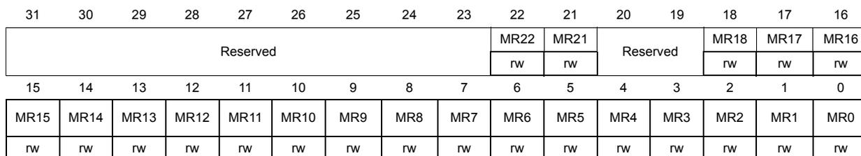
10.3.1 Interrupt mask register (EXTI_IMR)
Address offset: 0x00
Reset value: 0x0000 0000
| 31 | 30 | 29 | 28 | 27 | 26 | 25 | 24 | 23 | 22 | 21 | 20 | 19 | 18 | 17 | 16 | |
| Reserved | MR22 | MR21 | Reserved | MR18 | MR17 | MR16 | ||||||||||
| rw | rw | rw | rw | rw | ||||||||||||
| 15 | 14 | 13 | 12 | 11 | 10 | 9 | 8 | 7 | 6 | 5 | 4 | 3 | 2 | 1 | 0 | |
| MR15 | MR14 | MR13 | MR12 | MR11 | MR10 | MR9 | MR8 | MR7 | MR6 | MR5 | MR4 | MR3 | MR2 | MR1 | MR0 | |
| rw | rw | rw | rw | rw | rw | rw | rw | rw | rw | rw | rw | rw | rw | rw | rw | |
Bits 31:23 Reserved, must be kept at reset value.
Bits 22:0 MRx : Interrupt mask on line x
0: Interrupt request from line x is masked
1: Interrupt request from line x is not masked
10.3.2 Event mask register (EXTI_EMR)
Address offset: 0x04
Reset value: 0x0000 0000
| 31 | 30 | 29 | 28 | 27 | 26 | 25 | 24 | 23 | 22 | 21 | 20 | 19 | 18 | 17 | 16 | |
| Reserved | MR22 | MR21 | Reserved | MR18 | MR17 | MR16 | ||||||||||
| rw | rw | rw | rw | rw | ||||||||||||
| 15 | 14 | 13 | 12 | 11 | 10 | 9 | 8 | 7 | 6 | 5 | 4 | 3 | 2 | 1 | 0 | |
| MR15 | MR14 | MR13 | MR12 | MR11 | MR10 | MR9 | MR8 | MR7 | MR6 | MR5 | MR4 | MR3 | MR2 | MR1 | MR0 | |
| rw | rw | rw | rw | rw | rw | rw | rw | rw | rw | rw | rw | rw | rw | rw | rw | |
Bits 31:23 Reserved, must be kept at reset value.
Bits 22:0 MRx : Event mask on line x
0: Event request from line x is masked
1: Event request from line x is not masked
10.3.3 Rising trigger selection register (EXTI_RTSR)
Address offset: 0x08
Reset value: 0x0000 0000
| 31 | 30 | 29 | 28 | 27 | 26 | 25 | 24 | 23 | 22 | 21 | 20 | 19 | 18 | 17 | 16 |
|---|---|---|---|---|---|---|---|---|---|---|---|---|---|---|---|
| Reserved | TR22 | TR21 | Reserved | TR18 | TR17 | TR16 | |||||||||
| rw | rw | rw | rw | rw | |||||||||||
| 15 | 14 | 13 | 12 | 11 | 10 | 9 | 8 | 7 | 6 | 5 | 4 | 3 | 2 | 1 | 0 |
| TR15 | TR14 | TR13 | TR12 | TR11 | TR10 | TR9 | TR8 | TR7 | TR6 | TR5 | TR4 | TR3 | TR2 | TR1 | TR0 |
| rw | rw | rw | rw | rw | rw | rw | rw | rw | rw | rw | rw | rw | rw | rw | rw |
Bits 31:23 Reserved, must be kept at reset value.
Bits 22:0 TRx : Rising trigger event configuration bit of line x
0: Rising trigger disabled (for Event and Interrupt) for input line
1: Rising trigger enabled (for Event and Interrupt) for input line
Note: The external wake-up lines are edge triggered, no glitch must be generated on these lines. If a rising edge occurs on the external interrupt line while writing to the EXTI_RTSR register, the pending bit is set.
Rising and falling edge triggers can be set for the same interrupt line. In this configuration, both generate a trigger condition.
10.3.4 Falling trigger selection register (EXTI_FTSR)
Address offset: 0x0C
Reset value: 0x0000 0000
| 31 | 30 | 29 | 28 | 27 | 26 | 25 | 24 | 23 | 22 | 21 | 20 | 19 | 18 | 17 | 16 |
|---|---|---|---|---|---|---|---|---|---|---|---|---|---|---|---|
| Reserved | TR22 | TR21 | Reserved | TR18 | TR17 | TR16 | |||||||||
| rw | rw | rw | rw | rw | |||||||||||
| 15 | 14 | 13 | 12 | 11 | 10 | 9 | 8 | 7 | 6 | 5 | 4 | 3 | 2 | 1 | 0 |
| TR15 | TR14 | TR13 | TR12 | TR11 | TR10 | TR9 | TR8 | TR7 | TR6 | TR5 | TR4 | TR3 | TR2 | TR1 | TR0 |
| rw | rw | rw | rw | rw | rw | rw | rw | rw | rw | rw | rw | rw | rw | rw | rw |
Bits 31:23 Reserved, must be kept at reset value.
Bits 22:0 TRx : Falling trigger event configuration bit of line x
0: Falling trigger disabled (for Event and Interrupt) for input line
1: Falling trigger enabled (for Event and Interrupt) for input line.
Note: The external wake-up lines are edge triggered, no glitch must be generated on these lines. If a falling edge occurs on the external interrupt line while writing to the EXTI_FTSR register, the pending bit is not set.
Rising and falling edge triggers can be set for the same interrupt line. In this configuration, both generate a trigger condition.
10.3.5 Software interrupt event register (EXTI_SWIER)
Address offset: 0x10
Reset value: 0x0000 0000
| 31 | 30 | 29 | 28 | 27 | 26 | 25 | 24 | 23 | 22 | 21 | 20 | 19 | 18 | 17 | 16 |
|---|---|---|---|---|---|---|---|---|---|---|---|---|---|---|---|
| Reserved | SWIER 22 | SWIER 21 | Reserved | SWIER 18 | SWIER 17 | SWIER 16 | |||||||||
| rw | rw | rw | rw | rw | |||||||||||
| 15 | 14 | 13 | 12 | 11 | 10 | 9 | 8 | 7 | 6 | 5 | 4 | 3 | 2 | 1 | 0 |
| SWIER 15 | SWIER 14 | SWIER 13 | SWIER 12 | SWIER 11 | SWIER 10 | SWIER 9 | SWIER 8 | SWIER 7 | SWIER 6 | SWIER 5 | SWIER 4 | SWIER 3 | SWIER 2 | SWIER 1 | SWIER 0 |
| rw | rw | rw | rw | rw | rw | rw | rw | rw | rw | rw | rw | rw | rw | rw | rw |
Bits 31:23 Reserved, must be kept at reset value.
Bits 22:0 SWIERx : Software Interrupt on line x
If interrupt are enabled on line x in the EXTI_IMR register, writing '1' to SWIERx bit when it is set at '0' sets the corresponding pending bit in the EXTI_PR register, thus resulting in an interrupt request generation.
This bit is cleared by clearing the corresponding bit in EXTI_PR (by writing a 1 to the bit).
10.3.6 Pending register (EXTI_PR)
Address offset: 0x14
Reset value: 0x0000 0000
| 31 | 30 | 29 | 28 | 27 | 26 | 25 | 24 | 23 | 22 | 21 | 20 | 19 | 18 | 17 | 16 |
|---|---|---|---|---|---|---|---|---|---|---|---|---|---|---|---|
| Reserved | PR22 | PR21 | Reserved | PR18 | PR17 | PR16 | |||||||||
| rc_w1 | rc_w1 | rc_w1 | rc_w1 | rc_w1 | |||||||||||
| 15 | 14 | 13 | 12 | 11 | 10 | 9 | 8 | 7 | 6 | 5 | 4 | 3 | 2 | 1 | 0 |
| PR15 | PR14 | PR13 | PR12 | PR11 | PR10 | PR9 | PR8 | PR7 | PR6 | PR5 | PR4 | PR3 | PR2 | PR1 | PR0 |
| rc_w1 | rc_w1 | rc_w1 | rc_w1 | rc_w1 | rc_w1 | rc_w1 | rc_w1 | rc_w1 | rc_w1 | rc_w1 | rc_w1 | rc_w1 | rc_w1 | rc_w1 | rc_w1 |
Bits 31:23 Reserved, must be kept at reset value.
Bits 22:0 PRx : Pending bit
0: No trigger request occurred
1: selected trigger request occurred
This bit is set when the selected edge event arrives on the external interrupt line.
This bit is cleared by programming it to '1'.
10.3.7 EXTI register map
Table 39 gives the EXTI register map and the reset values.
Table 39. External interrupt/event controller register map and reset values
| Offset | Register | 31 | 30 | 29 | 28 | 27 | 26 | 25 | 24 | 23 | 22 | 21 | 20 | 19 | 18 | 17 | 16 | 15 | 14 | 13 | 12 | 11 | 10 | 9 | 8 | 7 | 6 | 5 | 4 | 3 | 2 | 1 | 0 |
|---|---|---|---|---|---|---|---|---|---|---|---|---|---|---|---|---|---|---|---|---|---|---|---|---|---|---|---|---|---|---|---|---|---|
| 0x00 | EXTI_IMR | Reserved | MR [22:21] | Reser ved | MR[18:0] | ||||||||||||||||||||||||||||
| Reset value | 0 0 | ||||||||||||||||||||||||||||||||
| 0x04 | EXTI_EMR | Reserved | MR [22:21] | Reser ved | MR[18:0] | ||||||||||||||||||||||||||||
| Reset value | 0 0 | ||||||||||||||||||||||||||||||||
| 0x08 | EXTI_RTSR | Reserved | TR [22:21] | Reser ved | TR[18:0] | ||||||||||||||||||||||||||||
| Reset value | 0 0 | ||||||||||||||||||||||||||||||||
| 0x0C | EXTI_FTSR | Reserved | TR [22:21] | Reser ved | TR[18:0] | ||||||||||||||||||||||||||||
| Reset value | 0 0 | ||||||||||||||||||||||||||||||||
| 0x10 | EXTI_SWIER | Reserved | SWIER [22:21] | Reser ved | SWIER[18:0] | ||||||||||||||||||||||||||||
| Reset value | 0 0 | ||||||||||||||||||||||||||||||||
| 0x14 | EXTI_PR | Reserved | PR [22:21] | Reser ved | PR[18:0] | ||||||||||||||||||||||||||||
| Reset value | 0 0 | ||||||||||||||||||||||||||||||||
Refer to Section 2.3: Memory map for the register boundary addresses.